Nanohardness of Sintered and Shock Deformed Alumina RIYA CHAKRABORTY, ARJUN DEY, ANOOP K. MUKHOPADHYAY, KESHAW D. JOSHI, AMIT RAV, ASHOK K. MANDAL, SANDIP BYSAKH, SAMPAD K. BISWAS, and SATISH C. GUPTA To understand how high–strain rate, flyer-plate impact affects the nanohardness of a coarse (~10 lm) grain, high-density (~3.978 gm cc –1 ) alumina, load controlled nanoindentation experiments were conducted with a Berkovich indenter on as-sintered disks and shock-recovered alumina fragments obtained from an earlier flyer-plate shock impact study. The nanohardness of the shock-recovered alumina was much lower than that of the as-sintered alumina. The indentation size effect was severe in the shock-recovered alumina but only mild in the as-sintered alumina. Extensive additional characterization by field emission scanning electron microscopy, transmission electron microscopy, and analysis of the experimental load depth data were used to provide a new explanation for the presence of strong indentation size effect in the shock- recovered alumina. Finally, a qualitative model was proposed to provide a rationale for the whole scenario of nanoindentation responses in the as-sintered and shock-recovered alumina ceramics. DOI: 10.1007/s11661-011-0900-z Ó The Minerals, Metals & Materials Society and ASM International 2011 I. INTRODUCTION ALUMINA is one of the most important structural ceramics suitable for applications involving both high- load and high–strain rate impact events. [1–27] All of such applications involve the measurement of hardness [1–9] at macro-, micro-, or nanoscale. Most of these measure- ments, [6–9] barring a few, [5] are on fine-grain and submi- crometer grain-sized alumina ceramics. The other major problem with most of the hardness data of alumina reported as a function of load is that it exhibits an indentation size effect, [10,11] thereby making it difficult to provide unique hardness data of alumina for design purposes. The indentation size effect (ISE) is usually manifested as a decrease in macro-, micro-, and nanoh- ardness with an increase in the indentation load and depth. It is well known that a wide variety of materials (e.g., metallic, ceramic, and quasi-crystalline) [10–13] exhibit ISE. Although numerous explanations have been proposed, [14–25] the basic cause of ISE in structural ceramics (e.g., polycrystalline alumina) is yet to be unequivocally established [12] because all of such explana- tions [14–22] or models [23–25] for ISE have their own limitations. [13,26] Thus, the basic objective of the present work was to use the nanoindentation technique to evaluate nanohardness of shock-recovered fragments of a coarse-grain (10 lm), high-density (3.978 gm cc –1 ) alumina obtained after a carefully conducted flyer-plate shock experiment, [27] and to examine if the nanohardness was similar to or degraded in comparison with that of the as-sintered alumina ceramics. As a result of this effort, we report for the first time a new explanation for the presence of strong ISE in shock-recovered alumina fragments obtained from an earlier study. [27] II. MATERIALS AND METHODS The samples used in the present work were alumina discs prepared by pressureless sintering at 1583 K (1310 °C) in air (dia ~48 mm, thickness ~2.5 mm, density ~3.978 gm cc –1 , and grain size ~10 lm). The commer- cially available 99.99 pct pure a-alumina powder (Morimura Bros. Inc., Tokyo, Japan), with an average particle size (d 50 ) of only 100 nm (Figure 1(a)) and a minor presence of impurities (e.g., Si, 12 ppm; Fe, 7 ppm; Na, 9 ppm; K, 3 ppm; Ca, 2 ppm; Mg, 2 ppm; and Cu, 1 ppm), was used in the present study to achieve low- temperature sintering. The scanning electron photomi- crograph of the thermally etched microstructure of the sintered alumina containing a typical nanoindentation array is shown in Figure 1(b). The alumina samples were deliberately shocked by an asymmetric flyer plate impact with a SS304 plate at a pressure of 6.5 GPa in a gas gun. [27–29] The shock-recovered alumina fragments had a large statistical variety of shapes and sizes, as depicted in the scanning electron photomicrograph in Figure 2, with RIYA CHAKRABORTY, Project Fellow, ASHOK K. MANDAL, Technical Officer, and ANOOP K. MUKHOPADHYAY, SANDIP BYSAKH, and SAMPAD K. BISWAS, Scientists, are with the Central Glass and Ceramic Research Institute, Council of Scientific and Industrial Research, Kolkata 700032, India. Contact e-mail: anoop- [email protected]ARJUN DEY, formerly Senior Research Fellow, with the Central Glass and Ceramic Research Institute, Council of Scientific and Industrial Research, is now a Scientist with the Thermal System Group, ISRO Satellite Centre (ISAC), Indian Space Research Organisation, Department of Space, Government of India, Bangalore 560017, India. KESHAW D. JOSHI, AMIT RAV, and SATISH C. GUPTA, Scientists, are with the Applied Physics Division, Bhabha Atomic Research Centre, Mumbai 400085, India. Riya Chakraborty and Arjun Dey contributed equally to this research work. Manuscript submitted February 28, 2011. Article published online October 15, 2011 METALLURGICAL AND MATERIALS TRANSACTIONS A VOLUME 43A, FEBRUARY 2012—459
Transcript
Nanohardness of Sintered and Shock Deformed Alumina
RIYA CHAKRABORTY, ARJUN DEY, ANOOP K. MUKHOPADHYAY,KESHAW D. JOSHI, AMIT RAV, ASHOK K. MANDAL, SANDIP BYSAKH,SAMPAD K. BISWAS, and SATISH C. GUPTA
To understand how high–strain rate, flyer-plate impact affects the nanohardness of a coarse(~10 lm) grain, high-density (~3.978 gm cc–1) alumina, load controlled nanoindentationexperiments were conducted with a Berkovich indenter on as-sintered disks and shock-recoveredalumina fragments obtained from an earlier flyer-plate shock impact study. The nanohardnessof the shock-recovered alumina was much lower than that of the as-sintered alumina. Theindentation size effect was severe in the shock-recovered alumina but only mild in the as-sinteredalumina. Extensive additional characterization by field emission scanning electron microscopy,transmission electron microscopy, and analysis of the experimental load depth data were used toprovide a new explanation for the presence of strong indentation size effect in the shock-recovered alumina. Finally, a qualitative model was proposed to provide a rationale for thewhole scenario of nanoindentation responses in the as-sintered and shock-recovered aluminaceramics.
DOI: 10.1007/s11661-011-0900-z� The Minerals, Metals & Materials Society and ASM International 2011
I. INTRODUCTION
ALUMINA is one of the most important structuralceramics suitable for applications involving both high-load and high–strain rate impact events.[1–27] All of suchapplications involve the measurement of hardness[1–9] atmacro-, micro-, or nanoscale. Most of these measure-ments,[6–9] barring a few,[5] are on fine-grain and submi-crometer grain-sized alumina ceramics. The other majorproblem with most of the hardness data of aluminareported as a function of load is that it exhibits anindentation size effect,[10,11] thereby making it difficult toprovide unique hardness data of alumina for designpurposes. The indentation size effect (ISE) is usuallymanifested as a decrease in macro-, micro-, and nanoh-ardness with an increase in the indentation load anddepth. It is well known that a wide variety of materials(e.g., metallic, ceramic, and quasi-crystalline)[10–13]
exhibit ISE. Although numerous explanations have beenproposed,[14–25] the basic cause of ISE in structuralceramics (e.g., polycrystalline alumina) is yet to be
unequivocally established[12] because all of such explana-tions[14–22] or models[23–25] for ISE have their ownlimitations.[13,26] Thus, the basic objective of the presentwork was to use the nanoindentation technique toevaluate nanohardness of shock-recovered fragments ofa coarse-grain (10 lm), high-density (3.978 gm cc–1)alumina obtained after a carefully conducted flyer-plateshock experiment,[27] and to examine if the nanohardnesswas similar to or degraded in comparison with that of theas-sintered alumina ceramics. As a result of this effort, wereport for the first time a new explanation for the presenceof strong ISE in shock-recovered alumina fragmentsobtained from an earlier study.[27]
II. MATERIALS AND METHODS
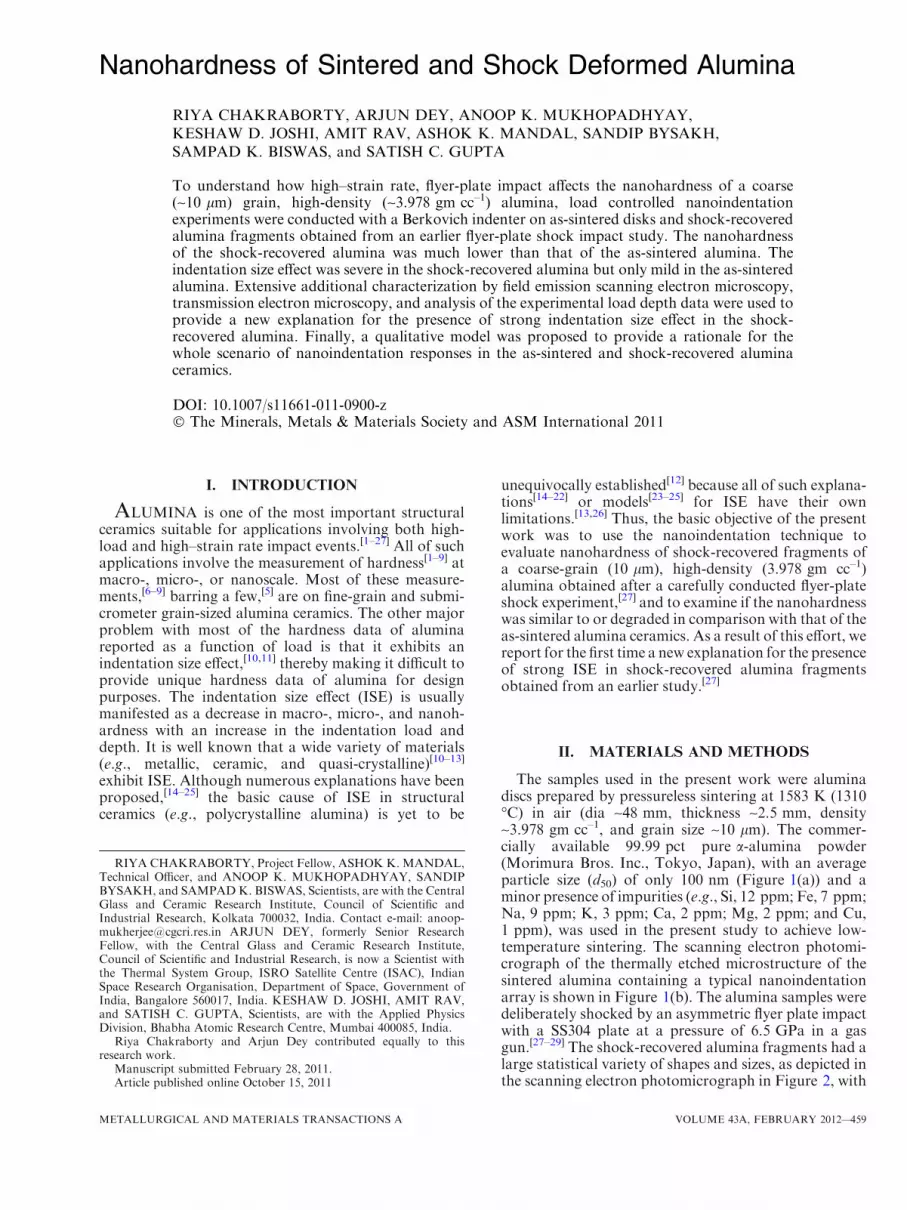
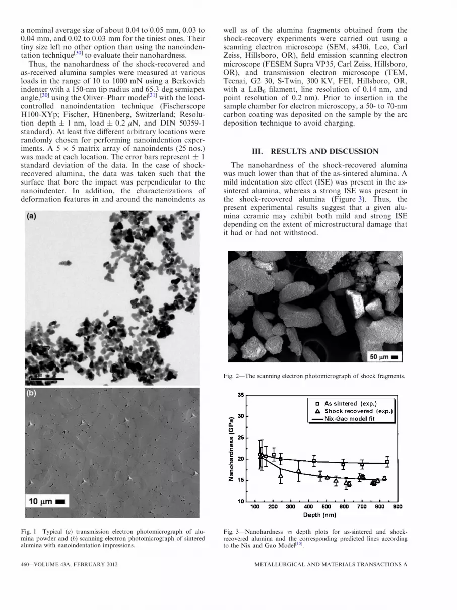
The samples used in the present work were aluminadiscs prepared by pressureless sintering at 1583 K (1310�C) in air (dia ~48 mm, thickness ~2.5 mm, density~3.978 gm cc–1, and grain size ~10 lm). The commer-cially available 99.99 pct pure a-alumina powder(Morimura Bros. Inc., Tokyo, Japan), with an averageparticle size (d50) of only 100 nm (Figure 1(a)) and aminor presence of impurities (e.g., Si, 12 ppm; Fe, 7 ppm;Na, 9 ppm; K, 3 ppm; Ca, 2 ppm; Mg, 2 ppm; and Cu,1 ppm), was used in the present study to achieve low-temperature sintering. The scanning electron photomi-crograph of the thermally etched microstructure of thesintered alumina containing a typical nanoindentationarray is shown in Figure 1(b). The alumina samples weredeliberately shocked by an asymmetric flyer plate impactwith a SS304 plate at a pressure of 6.5 GPa in a gasgun.[27–29] The shock-recovered alumina fragments had alarge statistical variety of shapes and sizes, as depicted inthe scanning electron photomicrograph in Figure 2, with
RIYA CHAKRABORTY, Project Fellow, ASHOKK. MANDAL,Technical Officer, and ANOOP K. MUKHOPADHYAY, SANDIPBYSAKH, and SAMPADK. BISWAS, Scientists, are with the CentralGlass and Ceramic Research Institute, Council of Scientific andIndustrial Research, Kolkata 700032, India. Contact e-mail: [email protected] ARJUN DEY, formerly Senior ResearchFellow, with the Central Glass and Ceramic Research Institute,Council of Scientific and Industrial Research, is now a Scientist withthe Thermal System Group, ISRO Satellite Centre (ISAC), IndianSpace Research Organisation, Department of Space, Government ofIndia, Bangalore 560017, India. KESHAW D. JOSHI, AMIT RAV,and SATISH C. GUPTA, Scientists, are with the Applied PhysicsDivision, Bhabha Atomic Research Centre, Mumbai 400085, India.
Riya Chakraborty and Arjun Dey contributed equally to thisresearch work.
Manuscript submitted February 28, 2011.Article published online October 15, 2011
METALLURGICAL AND MATERIALS TRANSACTIONS A VOLUME 43A, FEBRUARY 2012—459
a nominal average size of about 0.04 to 0.05 mm, 0.03 to0.04 mm, and 0.02 to 0.03 mm for the tiniest ones. Theirtiny size left no other option than using the nanoinden-tation technique[30] to evaluate their nanohardness.
Thus, the nanohardness of the shock-recovered andas-received alumina samples were measured at variousloads in the range of 10 to 1000 mN using a Berkovichindenter with a 150-nm tip radius and 65.3 deg semiapexangle,[30] using the Oliver–Pharr model[31] with the load-controlled nanoindentation technique (FischerscopeH100-XYp; Fischer, Hunenberg, Switzerland; Resolu-tion depth ± 1 nm, load ± 0.2 lN, and DIN 50359-1standard). At least five different arbitrary locations wererandomly chosen for performing nanoindention exper-iments. A 5 9 5 matrix array of nanoindents (25 nos.)was made at each location. The error bars represent ± 1standard deviation of the data. In the case of shock-recovered alumina, the data was taken such that thesurface that bore the impact was perpendicular to thenanoindenter. In addition, the characterizations ofdeformation features in and around the nanoindents as
well as of the alumina fragments obtained from theshock-recovery experiments were carried out using ascanning electron microscope (SEM, s430i, Leo, CarlZeiss, Hillsboro, OR), field emission scanning electronmicroscope (FESEM Supra VP35, Carl Zeiss, Hillsboro,OR), and transmission electron microscope (TEM,Tecnai, G2 30, S-Twin, 300 KV, FEI, Hillsboro, OR,with a LaB6 filament, line resolution of 0.14 nm, andpoint resolution of 0.2 nm). Prior to insertion in thesample chamber for electron microscopy, a 50- to 70-nmcarbon coating was deposited on the sample by the arcdeposition technique to avoid charging.
III. RESULTS AND DISCUSSION
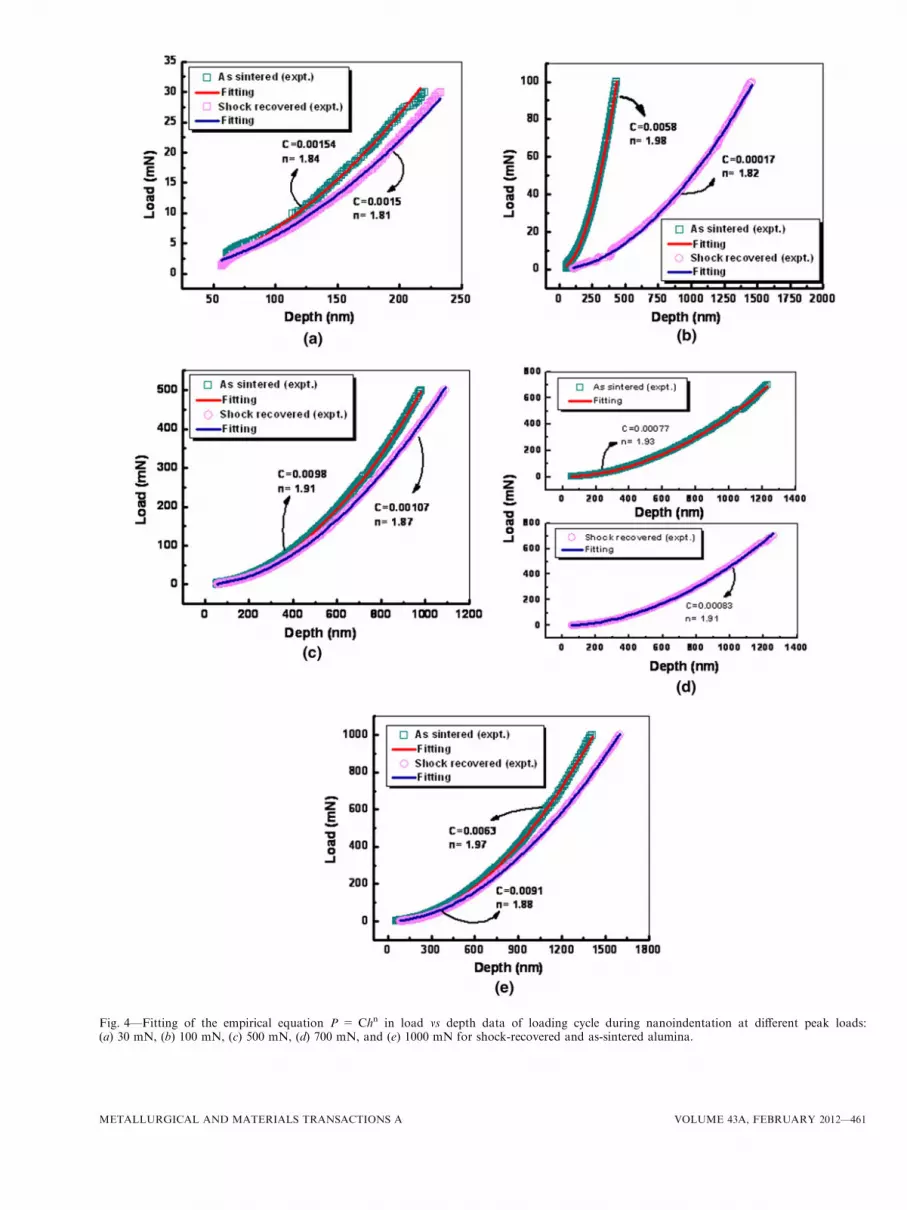
The nanohardness of the shock-recovered aluminawas much lower than that of the as-sintered alumina. Amild indentation size effect (ISE) was present in the as-sintered alumina, whereas a strong ISE was present inthe shock-recovered alumina (Figure 3). Thus, thepresent experimental results suggest that a given alu-mina ceramic may exhibit both mild and strong ISEdepending on the extent of microstructural damage thatit had or had not withstood.
Fig. 2—The scanning electron photomicrograph of shock fragments.
Fig. 3—Nanohardness vs depth plots for as-sintered and shock-recovered alumina and the corresponding predicted lines accordingto the Nix and Gao Model[15].
Fig. 1—Typical (a) transmission electron photomicrograph of alu-mina powder and (b) scanning electron photomicrograph of sinteredalumina with nanoindentation impressions.
460—VOLUME 43A, FEBRUARY 2012 METALLURGICAL AND MATERIALS TRANSACTIONS A
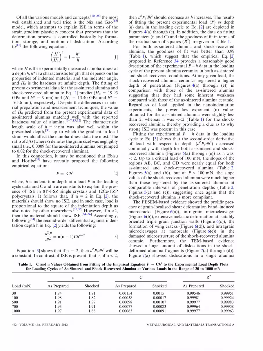
Fig. 4—Fitting of the empirical equation P = Chn in load vs depth data of loading cycle during nanoindentation at different peak loads:(a) 30 mN, (b) 100 mN, (c) 500 mN, (d) 700 mN, and (e) 1000 mN for shock-recovered and as-sintered alumina.
METALLURGICAL AND MATERIALS TRANSACTIONS A VOLUME 43A, FEBRUARY 2012—461
Of all the various models and concepts,[10–25] the mostwell established and well tried is the Nix and Gao[15]
model, which attempts to explain ISE in terms of thestrain gradient plasticity concept that proposes that thedeformation process is controlled basically by forma-tion, storage, and motion of dislocation. Accordingto[15] the following equation:
H
H0
� �2
¼ 1þ h�
h½1�
whereH is the experimentally measured nanohardness ata depth h, h* is a characteristic length that depends on theproperties of indented material and the indenter angle,and H0 is the hardness at infinite depth. The fitting ofpresent experimental data for the as-sintered alumina andshock-recovered alumina to Eq. [1] predict (H0 = 19.93GPa and h* = 9 nm) and (H0 = 13.40 GPa and h* =165.6 nm), respectively. Despite the differences in mate-rial preparation and measurement techniques, the valueof H0 predicted from the present experimental data ofas-sintered alumina matched well with the reportedhardness value of alumina.[5–7,13,32] The characteristiclength scale of h = 9 nm was also well within theprescribed depth,[33] up to which the gradient in localstrain would affect the nanohardness data the most. Theratioof h/G (whereGdenotes the grain size)was negligiblysmall (i.e., 0.0009 for the as-sintered alumina but jumpedto 0.02 for the shock-recovered alumina).
In this connection, it may be mentioned that Ebisuand Horibe[34] have recently proposed the followingempirical equation:
P ¼ Chn ½2�
where, h is indentation depth at a load P in the loadingcycle data and C and n are constants to explain the pres-ence of ISE in 8Y-FSZ single crystals and 12Ce-TZPpolycrystals. It follows that, if n = 2 in Eq. [2], thematerials should show no ISE, and in such case, load isproportional to the square of the indentation depth asalso noted by other researchers.[35,36] However, if n<2,then the material should show ISE.[34–36] Accordingly,following[34] the second-order differential against inden-tation depth h in Eq. [2] yields the following:
d2P
dh2¼ n n� 1ð ÞChn�2 ½3�
Equation [3] shows that if n = 2, then d2P/dh2 will bea constant. In contrast, if ISE is present, that is, if n< 2,
then d2P/dh2 should decrease as h increases. The resultsof fitting the present experimental load (P) vs depth(h) data in the loading cycle to Eq. [2] are depicted inFigures 4(a) through (e). In addition, the data on fittingparameters (n and C) and the goodness of fit in terms ofthe residual sum of squares (R2) are given in Table 1.For both as-sintered alumina and shock-recovered
alumina, the goodness of fit was better than 0.99(Table 1), which suggest that the empirical Eq. [2]proposed in Reference 34 provides a reasonably gooddescription of the experimental P – h data in the loadingcycle of the present alumina ceramics in both as-sinteredand shock-recovered conditions. At any given load, theshock-recovered alumina ceramics registered a higherdepth of penetration (Figures 4(a) through (e)) incomparison with those of the as-sintered aluminasuggesting that they had some inherent weaknesscompared with those of the as-sintered alumina ceramic.Regardless of load applied in the nanoindentationexperiments, the power law exponent (n) valuesobtained for the as-sintered alumina were slightly lessthan 2, whereas n was <<2 (Table 1) for the shock-recovered alumina, thereby providing a clue as to whystrong ISE was present in this case.Fitting the experimental P – h data in the loading
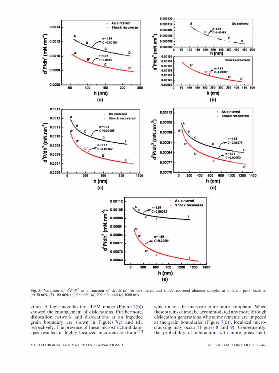
cycle to Eq. [3] shows that the second-order derivativeof load with respect to depth (d2P/dh2) decreasedcontinually with depth for both as-sintered and shock-recovered alumina (Figures 5(a) through (e)) as n was< 2. Up to a critical load of 100 mN, the slopes of theregions AB, BC, and CD were nearly equal for bothas-sintered and shock-recovered alumina (Table 2,Figures 5(a) and (b)), but at P> 100 mN, the slopevalues of the shock-recovered alumina were much higherthan those registered by the as-sintered alumina atcomparable intervals of penetration depths (Table 2,Figures 5(c) and (e)), suggesting once again that theshock-recovered alumina is more compliant.The FESEM-based evidence showed the prolific pres-
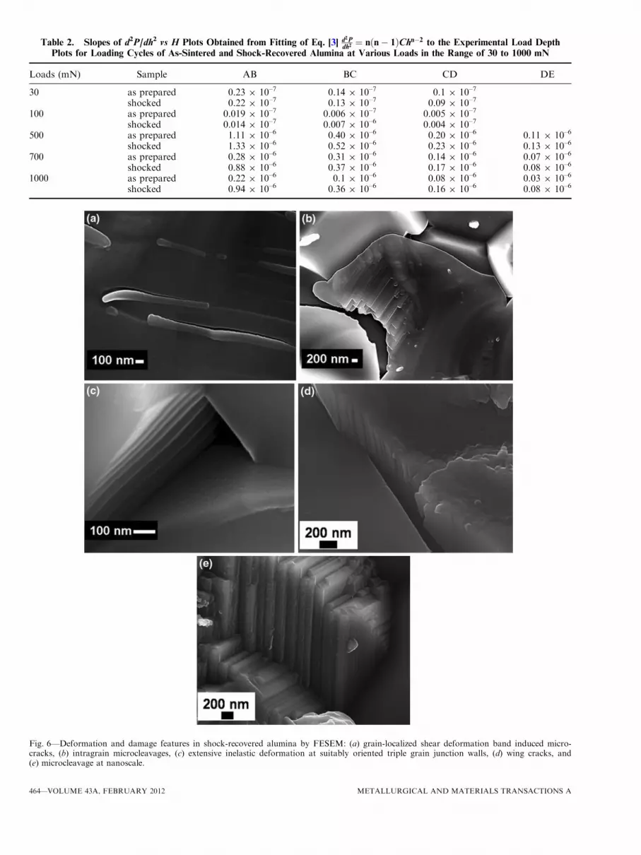
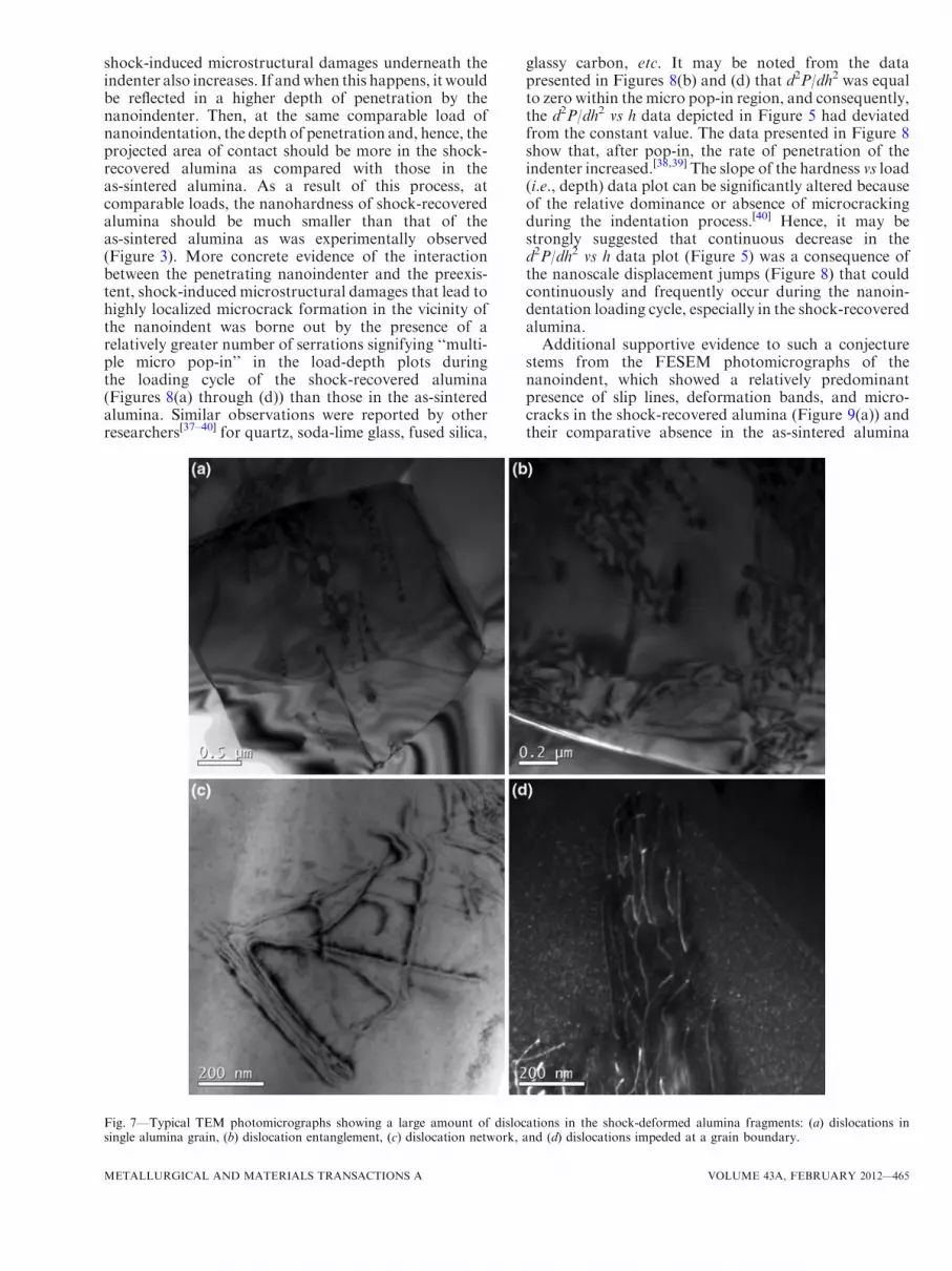
ence of grain-localized shear deformation band–inducedmicrocracks (Figure 6(a)), intragrain microcleavages(Figure 6(b)), extensive inelastic deformation at suitablyoriented triple grain junction walls (Figure 6(c)), theformation of wing cracks (Figure 6(d)), and intragrainmicrocleavages at nanoscale (Figure 6(e)) in thedamaged microstructure of the shock-recovered aluminaceramic. Furthermore, the TEM-based evidenceshowed a huge amount of dislocations in the shock-deformed alumina fragments (Figure 7(a) through (d)).Figure 7(a) showed dislocations in a single alumina
Table 1. C and n Values Obtained from Fitting of the Empirical Equation P = Chn to the Experimental Load Depth Plotsfor Loading Cycles of As-Sintered and Shock-Recovered Alumina at Various Loads in the Range of 30 to 1000 mN
Load (mN)
n C R2
As Prepared Shocked As Prepared Shocked As Prepared Shocked
462—VOLUME 43A, FEBRUARY 2012 METALLURGICAL AND MATERIALS TRANSACTIONS A
grain. A high-magnification TEM image (Figure 7(b))showed the entanglement of dislocations. Furthermore,dislocation network and dislocations at an impededgrain boundary are shown in Figures 7(c) and (d),respectively. The presence of these microstructural dam-ages resulted in highly localized microtensile strain,[37]
which made the microstructure more compliant. Whenthese strains cannot be accommodated any more throughdislocation generations whose movements are impededat the grain boundaries (Figure 7(d)), localized micro-cracking may occur (Figures 8 and 9). Consequently,the probability of interaction with more preexistent,
Fig. 5—Variation of d2P/dh2 as a function of depth (h) for as-sintered and shock-recovered alumina samples at different peak loads at(a) 30 mN, (b) 100 mN, (c) 500 mN, (d) 700 mN, and (e) 1000 mN.
METALLURGICAL AND MATERIALS TRANSACTIONS A VOLUME 43A, FEBRUARY 2012—463
Table 2. Slopes of d2P/dh2 vs H Plots Obtained from Fitting of Eq. [3] d2Pdh2¼ n n� 1ð ÞChn�2 to the Experimental Load Depth
Plots for Loading Cycles of As-Sintered and Shock-Recovered Alumina at Various Loads in the Range of 30 to 1000 mN
Fig. 6—Deformation and damage features in shock-recovered alumina by FESEM: (a) grain-localized shear deformation band induced micro-cracks, (b) intragrain microcleavages, (c) extensive inelastic deformation at suitably oriented triple grain junction walls, (d) wing cracks, and(e) microcleavage at nanoscale.
464—VOLUME 43A, FEBRUARY 2012 METALLURGICAL AND MATERIALS TRANSACTIONS A
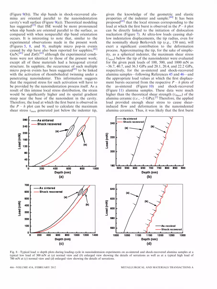
shock-induced microstructural damages underneath theindenter also increases. If andwhen this happens, it wouldbe reflected in a higher depth of penetration by thenanoindenter. Then, at the same comparable load ofnanoindentation, the depth of penetration and, hence, theprojected area of contact should be more in the shock-recovered alumina as compared with those in theas-sintered alumina. As a result of this process, atcomparable loads, the nanohardness of shock-recoveredalumina should be much smaller than that of theas-sintered alumina as was experimentally observed(Figure 3). More concrete evidence of the interactionbetween the penetrating nanoindenter and the preexis-tent, shock-induced microstructural damages that lead tohighly localized microcrack formation in the vicinity ofthe nanoindent was borne out by the presence of arelatively greater number of serrations signifying ‘‘multi-ple micro pop-in’’ in the load-depth plots duringthe loading cycle of the shock-recovered alumina(Figures 8(a) through (d)) than those in the as-sinteredalumina. Similar observations were reported by otherresearchers[37–40] for quartz, soda-lime glass, fused silica,
glassy carbon, etc. It may be noted from the datapresented in Figures 8(b) and (d) that d2P/dh2 was equalto zero within the micro pop-in region, and consequently,the d2P/dh2 vs h data depicted in Figure 5 had deviatedfrom the constant value. The data presented in Figure 8show that, after pop-in, the rate of penetration of theindenter increased.[38,39] The slope of the hardness vs load(i.e., depth) data plot can be significantly altered becauseof the relative dominance or absence of microcrackingduring the indentation process.[40] Hence, it may bestrongly suggested that continuous decrease in thed2P/dh2 vs h data plot (Figure 5) was a consequence ofthe nanoscale displacement jumps (Figure 8) that couldcontinuously and frequently occur during the nanoin-dentation loading cycle, especially in the shock-recoveredalumina.Additional supportive evidence to such a conjecture
stems from the FESEM photomicrographs of thenanoindent, which showed a relatively predominantpresence of slip lines, deformation bands, and micro-cracks in the shock-recovered alumina (Figure 9(a)) andtheir comparative absence in the as-sintered alumina
Fig. 7—Typical TEM photomicrographs showing a large amount of dislocations in the shock-deformed alumina fragments: (a) dislocations insingle alumina grain, (b) dislocation entanglement, (c) dislocation network, and (d) dislocations impeded at a grain boundary.
METALLURGICAL AND MATERIALS TRANSACTIONS A VOLUME 43A, FEBRUARY 2012—465
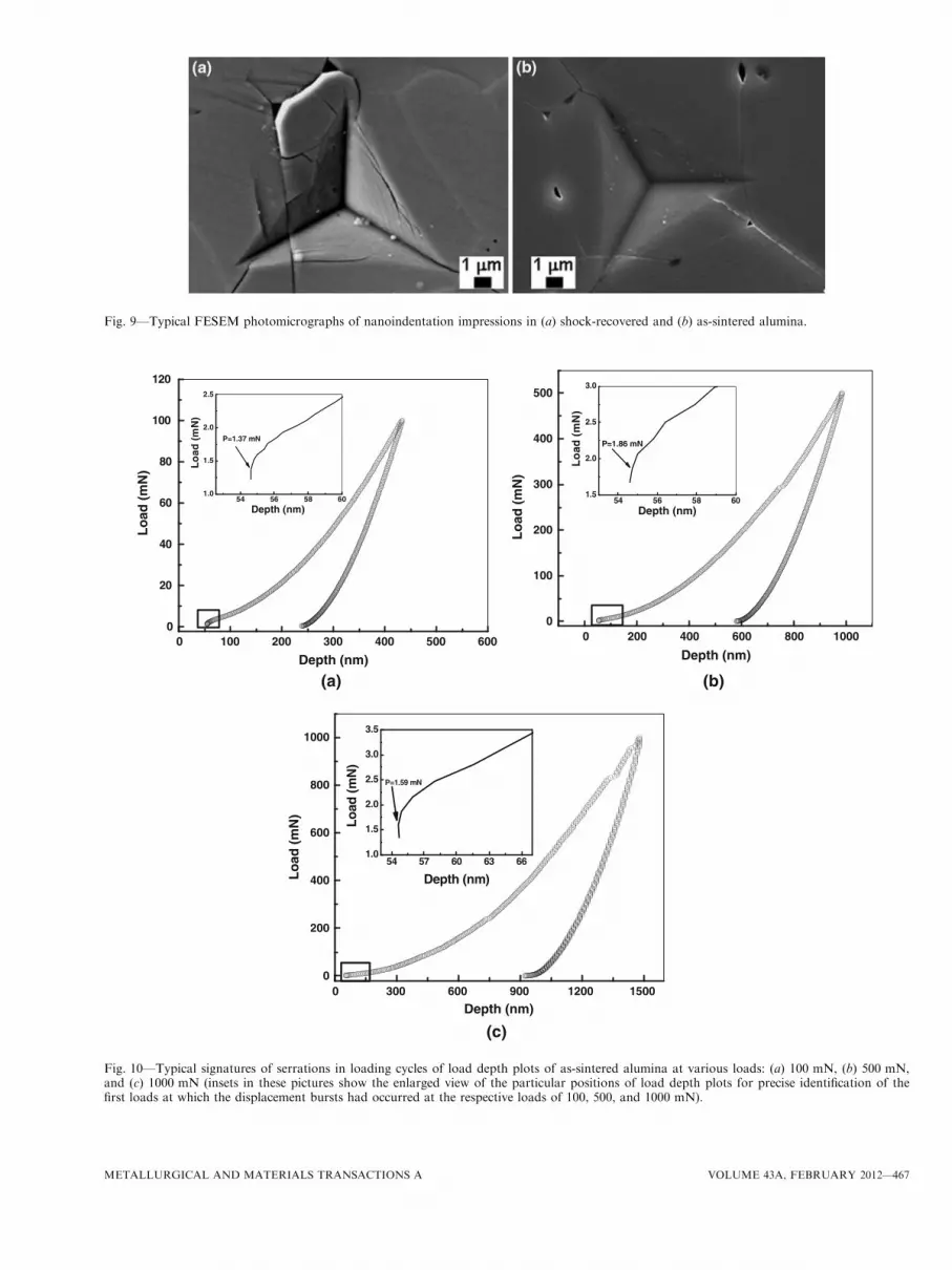
(Figure 9(b)). The slip bands in shock-recovered alu-mina are oriented parallel to the nanoindentationcavity’s wall surface (Figure 9(a)). Theoretical modelinghas suggested[25] that ISE would be more pronouncedwhen slip bands are oriented parallel to the surface, ascompared with when nonparallel slip band orientationoccurs. It is interesting to note that, similar to theexperimental observations made in the present work(Figures 5, 8, and 9), multiple micro pop-in eventscaused by slip have also been reported for sapphire,[41]
GaN,[42] and ZnO,[43] although the experimental condi-tions were not identical to those of the present work;except all of these materials had a hexagonal crystalstructure. In sapphire, the occurrence of such multiplemicro pop-in events has been suggested[41] to be linkedwith the activation of rhombohedral twinning under apenetrating nanoindenter. This information suggeststhat the required stress for such activation will have tobe provided by the nanoindentation process itself. As aresult of this intense local stress distribution, the strainwould be significantly higher and its spatial gradientsteep near the base of the nanoindent in the cavity.Therefore, the load at which the first burst is observed inthe P – h plot can be used to calculate the maximumshear stress smax generated just below the indenter tip,
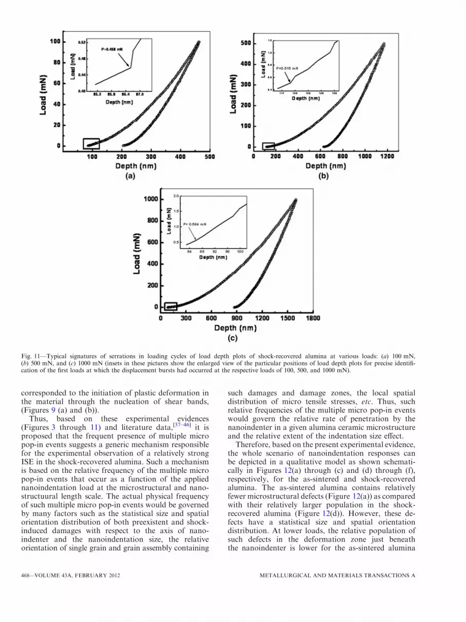
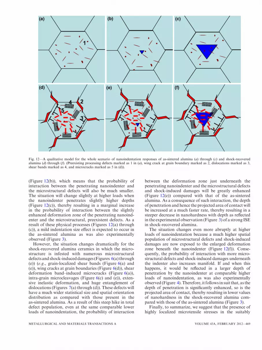
given the knowledge of the geometric and elasticproperties of the indenter and sample.[44] It has beenproposed[45] that the local stresses corresponding to theload at which the first burst is observed in the P – h plotcan be directly linked to the initiation of dislocationnucleation (Figure 7). At ultra-low loads causing shal-low indentation displacements, the tip radius, even forthe nominally sharp Berkovich tip (e.g., 150 nm), willexert a significant contribution to the deformationprocess. Approximating the tip, for the sake of simplic-ity, as a spherical indenter, the maximum shear stress(smax) below the tip of the nanoindenter were evaluatedfor the given peak loads of 100, 500, and 1000 mN as~36.7, 40.7, and 36.3 GPa and 20.1, 20.4, and 22.2 GPa,respectively, for the as-sintered and shock-recoveredalumina samples—following References 45 and 46—andthe appropriate load values at which the first displace-ment bursts occurred from the respective P – h plots ofthe as-sintered (Figure 10) and shock-recovered(Figure 11) alumina samples. These data were muchhigher than the theoretical shear strength (stheor) of thealumina ceramic (i.e., ~3 GPa).[1] Therefore, the appliedload provided enough shear stress to cause shear-induced flow and deformation in the nanoindentedalumina ceramics. Thus, it was likely that the first burst
Fig. 8—Typical load vs depth plots during loading cycle in nanoindentaion experiments on as-sintered and shock-recovered alumina samples at atypical low load of 300 mN at (a) normal view and (b) enlarged view showing the details of serrations as well as at a typical high load of700 mN at (c) normal view and (d) enlarged view showing the details of serrations.
466—VOLUME 43A, FEBRUARY 2012 METALLURGICAL AND MATERIALS TRANSACTIONS A
Fig. 9—Typical FESEM photomicrographs of nanoindentation impressions in (a) shock-recovered and (b) as-sintered alumina.
0 100 200 300 400 500 6000
20
40
60
80
100
120
54 56 58 601.0
1.5
2.0
2.5
Lo
ad (
mN
)
Depth (nm)
P=1.37 mN
Lo
ad (
mN
)
Depth (nm)
(a)
0 200 400 600 800 10000
100
200
300
400
500
54 56 58 601.5
2.0
2.5
3.0
Lo
ad (
mN
)
Depth (nm)
P=1.86 mN
Lo
ad (
mN
)
Depth (nm)
(b)
0 300 600 900 1200 15000
200
400
600
800
1000
54 57 60 63 661.0
1.5
2.0
2.5
3.0
3.5
Lo
ad (
mN
)
Depth (nm)
P=1.59 mN
Lo
ad (
mN
)
Depth (nm)
(c)
Fig. 10—Typical signatures of serrations in loading cycles of load depth plots of as-sintered alumina at various loads: (a) 100 mN, (b) 500 mN,and (c) 1000 mN (insets in these pictures show the enlarged view of the particular positions of load depth plots for precise identification of thefirst loads at which the displacement bursts had occurred at the respective loads of 100, 500, and 1000 mN).
METALLURGICAL AND MATERIALS TRANSACTIONS A VOLUME 43A, FEBRUARY 2012—467
corresponded to the initiation of plastic deformation inthe material through the nucleation of shear bands,(Figures 9 (a) and (b)).
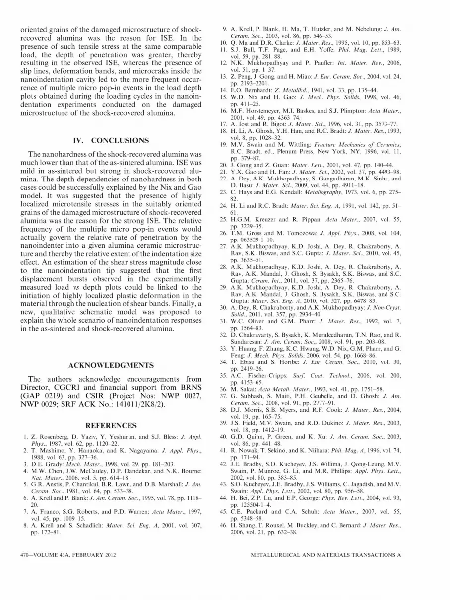
Thus, based on these experimental evidences(Figures 3 through 11) and literature data,[37–46] it isproposed that the frequent presence of multiple micropop-in events suggests a generic mechanism responsiblefor the experimental observation of a relatively strongISE in the shock-recovered alumina. Such a mechanismis based on the relative frequency of the multiple micropop-in events that occur as a function of the appliednanoindentation load at the microstructural and nano-structuural length scale. The actual physical frequencyof such multiple micro pop-in events would be governedby many factors such as the statistical size and spatialorientation distribution of both preexistent and shock-induced damages with respect to the axis of nano-indenter and the nanoindentation size, the relativeorientation of single grain and grain assembly containing
such damages and damage zones, the local spatialdistribution of micro tensile stresses, etc. Thus, suchrelative frequencies of the multiple micro pop-in eventswould govern the relative rate of penetration by thenanoindenter in a given alumina ceramic microstructureand the relative extent of the indentation size effect.Therefore, based on the present experimental evidence,
the whole scenario of nanoindentation responses canbe depicted in a qualitative model as shown schemati-cally in Figures 12(a) through (c) and (d) through (f),respectively, for the as-sintered and shock-recoveredalumina. The as-sintered alumina contains relativelyfewer microstructural defects (Figure 12(a)) as comparedwith their relatively larger population in the shock-recovered alumina (Figure 12(d)). However, these de-fects have a statistical size and spatial orientationdistribution. At lower loads, the relative population ofsuch defects in the deformation zone just beneaththe nanoindenter is lower for the as-sintered alumina
Fig. 11—Typical signatures of serrations in loading cycles of load depth plots of shock-recovered alumina at various loads: (a) 100 mN,(b) 500 mN, and (c) 1000 mN (insets in these pictures show the enlarged view of the particular positions of load depth plots for precise identifi-cation of the first loads at which the displacement bursts had occurred at the respective loads of 100, 500, and 1000 mN).
468—VOLUME 43A, FEBRUARY 2012 METALLURGICAL AND MATERIALS TRANSACTIONS A
(Figure 12(b)), which means that the probability ofinteraction between the penetrating nanoindenter andthe microstructural defects will also be much smaller.The situation will change slightly at higher loads whenthe nanoindenter penetrates slightly higher depths(Figure 12(c)), thereby resulting in a marginal increasein the probability of interaction between the slightlyenhanced deformation zone of the penetrating nanoind-enter and the microstructural, preexistent defects. As aresult of these physical processes (Figures 12(a) through(c)), a mild indentation size effect is expected to occur inthe as-sintered alumina as was also experimentallyobserved (Figure 3).
However, the situation changes dramatically for theshock-recovered alumina ceramics in which the micro-structure is infested with numerous microstructuraldefectsandshock-induceddamages (Figures 6(a) through(e)) (e.g., grain-localized shear bands (Figure 6(a) and(e)), wing cracks at grain boundaries (Figure 6(d)), sheardeformation band–induced microcracks (Figure 6(a)),intra-grain microcleavages (Figure 6(c) and (e)), exten-sive inelastic deformation, and huge entanglement ofdislocations (Figures 7(a) through (d)). These defects willhave a much wider statistical size and spatial orientationdistribution as compared with those present in theas-sintered alumina. As a result of this steep hike in totaldefect population, even at the same comparable lowerloads of nanoindentation, the probability of interaction
between the deformation zone just underneath thepenetrating nanoindenter and the microstructural defectsand shock-induced damages will be greatly enhanced(Figure 12(e)) compared with that of the as-sinteredalumina. As a consequence of such interaction, the depthof penetration and hence the projected area of contact willbe increased at a much faster rate, thereby resulting in asteeper decrease in nanohardness with depth as reflectedin the experimental observation (Figure 3) of a strong ISEin shock-recovered alumina.The situation changes even more abruptly at higher
loads of nanoindentation because a much higher spatialpopulation of microstructural defects and shock-induceddamages are now exposed to the enlarged deformationzone beneath the nanoindenter (Figure 12(f)). Conse-quently, the probability of interaction with more micro-structural defects and shock-induced damages underneaththe indenter also increases manifold. If and when thishappens, it would be reflected in a larger depth ofpenetration by the nanoindenter at comparable higherloads of nanoindentation, as was also experimentallyobserved (Figure 4).Therefore, it follows in suit that, as thedepth of penetration is significantly enhanced, so is theprojected area of contact, thereby resulting in lower valuesof nanohardness in the shock-recovered alumina com-pared with those of the as-sintered alumina (Figure 3).Finally, to summarize, we suggest that the presence of
highly localized microtensile stresses in the suitably
Fig. 12—A qualitative model for the whole scenario of nanoindentation responses of as-sintered alumina (a) through (c) and shock-recoveredalumina (d) through (f). (Preexisting processing defects marked as 1 in (a), wing crack at grain boundary marked as 2, dislocations marked as 3,shear bands marked as 4, and microcracks marked as 5 in (d)).
METALLURGICAL AND MATERIALS TRANSACTIONS A VOLUME 43A, FEBRUARY 2012—469
oriented grains of the damaged microstructure of shock-recovered alumina was the reason for ISE. In thepresence of such tensile stress at the same comparableload, the depth of penetration was greater, therebyresulting in the observed ISE, whereas the presence ofslip lines, deformation bands, and microcraks inside thenanoindentation cavity led to the more frequent occur-rence of multiple micro pop-in events in the load depthplots obtained during the loading cycles in the nanoin-dentation experiments conducted on the damagedmicrostructure of the shock-recovered alumina.
IV. CONCLUSIONS
The nanohardness of the shock-recovered alumina wasmuch lower than that of the as-sintered alumina. ISE wasmild in as-sintered but strong in shock-recovered alu-mina. The depth dependencies of nanohardness in bothcases could be successfully explained by the Nix and Gaomodel. It was suggested that the presence of highlylocalized microtensile stresses in the suitably orientedgrains of the damaged microstructure of shock-recoveredalumina was the reason for the strong ISE. The relativefrequency of the multiple micro pop-in events wouldactually govern the relative rate of penetration by thenanoindenter into a given alumina ceramic microstruc-ture and thereby the relative extent of the indentation sizeeffect. An estimation of the shear stress magnitude closeto the nanoindentation tip suggested that the firstdisplacement bursts observed in the experimentallymeasured load vs depth plots could be linked to theinitiation of highly localized plastic deformation in thematerial through the nucleation of shear bands. Finally, anew, qualitative schematic model was proposed toexplain the whole scenario of nanoindentation responsesin the as-sintered and shock-recovered alumina.
ACKNOWLEDGMENTS
The authors acknowledge encouragements fromDirector, CGCRI and financial support from BRNS(GAP 0219) and CSIR (Project Nos: NWP 0027,NWP 0029; SRF ACK No.: 141011/2K8/2).
REFERENCES1. Z. Rosenberg, D. Yaziv, Y. Yeshurun, and S.J. Bless: J. Appl.
Phys., 1987, vol. 62, pp. 1120–22.2. T. Mashimo, Y. Hanaoka, and K. Nagayama: J. Appl. Phys.,
1988, vol. 63, pp. 327–36.3. D.E. Grady: Mech. Mater., 1998, vol. 29, pp. 181–203.4. M.W. Chen, J.W. McCauley, D.P. Dandekar, and N.K. Bourne:
Nat. Mater., 2006, vol. 5, pp. 614–18.5. G.R. Anstis, P. Chantikul, B.R. Lawn, and D.B. Marshall: J. Am.
Ceram. Soc., 1981, vol. 64, pp. 533–38.6. A. Krell and P. Blank: J. Am. Ceram. Soc., 1995, vol. 78, pp. 1118–
20.7. A. Franco, S.G. Roberts, and P.D. Warren: Acta Mater., 1997,
vol. 45, pp. 1009–15.8. A. Krell and S. Schadlich: Mater. Sci. Eng. A, 2001, vol. 307,
pp. 172–81.
9. A. Krell, P. Blank, H. Ma, T. Hutzler, and M. Nebelung: J. Am.Ceram. Soc., 2003, vol. 86, pp. 546–53.
10. Q. Ma and D.R. Clarke: J. Mater. Res., 1995, vol. 10, pp. 853–63.11. S.J. Bull, T.F. Page, and E.H. Yoffe: Phil. Mag. Lett., 1989,
vol. 59, pp. 281–88.12. N.K. Mukhopadhyay and P. Paufler: Int. Mater. Rev., 2006,
vol. 51, pp. 1–37.13. Z. Peng, J. Gong, and H. Miao: J. Eur. Ceram. Soc., 2004, vol. 24,
pp. 2193–2201.14. E.O. Bernhardt: Z. Metallkd., 1941, vol. 33, pp. 135–44.15. W.D. Nix and H. Gao: J. Mech. Phys. Solids, 1998, vol. 46,
pp. 411–25.16. M.F. Horstemeyer, M.I. Baskes, and S.J. Plimpton: Acta Mater.,
2001, vol. 49, pp. 4363–74.17. A. Iost and R. Bigot: J. Mater. Sci., 1996, vol. 31, pp. 3573–77.18. H. Li, A. Ghosh, Y.H. Han, and R.C. Bradt: J. Mater. Res., 1993,
vol. 8, pp. 1028–32.19. M.V. Swain and M. Wittling: Fracture Mechanics of Ceramics,
R.C. Bradt, ed., Plenum Press, New York, NY, 1996, vol. 11,pp. 379–87.
20. J. Gong and Z. Guan: Mater. Lett., 2001, vol. 47, pp. 140–44.21. Y.X. Gao and H. Fan: J. Mater. Sci., 2002, vol. 37, pp. 4493–98.22. A. Dey, A.K. Mukhopadhyay, S. Gangadharan, M.K. Sinha, and
D. Basu: J. Mater. Sci., 2009, vol. 44, pp. 4911–18.23. C. Hays and E.G. Kendall: Metallography, 1973, vol. 6, pp. 275–
82.24. H. Li and R.C. Bradt: Mater. Sci. Eng. A, 1991, vol. 142, pp. 51–
61.25. H.G.M. Kreuzer and R. Pippan: Acta Mater., 2007, vol. 55,
pp. 3229–35.26. T.M. Gross and M. Tomozowa: J. Appl. Phys., 2008, vol. 104,
pp. 063529-1–10.27. A.K. Mukhopadhyay, K.D. Joshi, A. Dey, R. Chakraborty, A.
Rav, S.K. Biswas, and S.C. Gupta: J. Mater. Sci., 2010, vol. 45,pp. 3635–51.
28. A.K. Mukhopadhyay, K.D. Joshi, A. Dey, R. Chakraborty, A.Rav, A.K. Mandal, J. Ghosh, S. Bysakh, S.K. Biswas, and S.C.Gupta: Ceram. Int., 2011, vol. 37, pp. 2365–76.
29. A.K. Mukhopadhyay, K.D. Joshi, A. Dey, R. Chakraborty, A.Rav, A.K. Mandal, J. Ghosh, S. Bysakh, S.K. Biswas, and S.C.Gupta: Mater. Sci. Eng. A, 2010, vol. 527, pp. 6478–83.
30. A. Dey, R. Chakraborty, and A.K. Mukhopadhyay: J. Non-Cryst.Solid., 2011, vol. 357, pp. 2934–40.
31. W.C. Oliver and G.M. Pharr: J. Mater. Res., 1992, vol. 7,pp. 1564–83.
32. D. Chakravarty, S. Bysakh, K. Muraleedharan, T.N. Rao, and R.Sundaresan: J. Am. Ceram. Soc., 2008, vol. 91, pp. 203–08.
33. Y. Huang, F. Zhang, K.C. Hwang, W.D. Nix, G.M. Pharr, and G.Feng: J. Mech. Phys. Solids, 2006, vol. 54, pp. 1668–86.
34. T. Ebisu and S. Horibe: J. Eur. Ceram. Soc., 2010, vol. 30,pp. 2419–26.
35. A.C. Fischer-Cripps: Surf. Coat. Technol., 2006, vol. 200,pp. 4153–65.
36. M. Sakai: Acta Metall. Mater., 1993, vol. 41, pp. 1751–58.37. G. Subhash, S. Maiti, P.H. Geubelle, and D. Ghosh: J. Am.
Ceram. Soc., 2008, vol. 91, pp. 2777–91.38. D.J. Morris, S.B. Myers, and R.F. Cook: J. Mater. Res., 2004,
vol. 19, pp. 165–75.39. J.S. Field, M.V. Swain, and R.D. Dukino: J. Mater. Res., 2003,
vol. 18, pp. 1412–19.40. G.D. Quinn, P. Green, and K. Xu: J. Am. Ceram. Soc., 2003,
vol. 86, pp. 441–48.41. R. Nowak, T. Sekino, and K. Niihara: Phil. Mag. A, 1996, vol. 74,
pp. 171–94.42. J.E. Bradby, S.O. Kucheyev, J.S. Willima, J. Qong-Leung, M.V.
Swain, P. Munroe, G. Li, and M.R. Phillips: Appl. Phys. Lett.,2002, vol. 80, pp. 383–85.
43. S.O. Kucheyev, J.E. Bradby, J.S. Williams, C. Jagadish, and M.V.Swain: Appl. Phys. Lett., 2002, vol. 80, pp. 956–58.
44. H. Bei, Z.P. Lu, and E.P. George: Phys. Rev. Lett., 2004, vol. 93,pp. 125504-1–4.