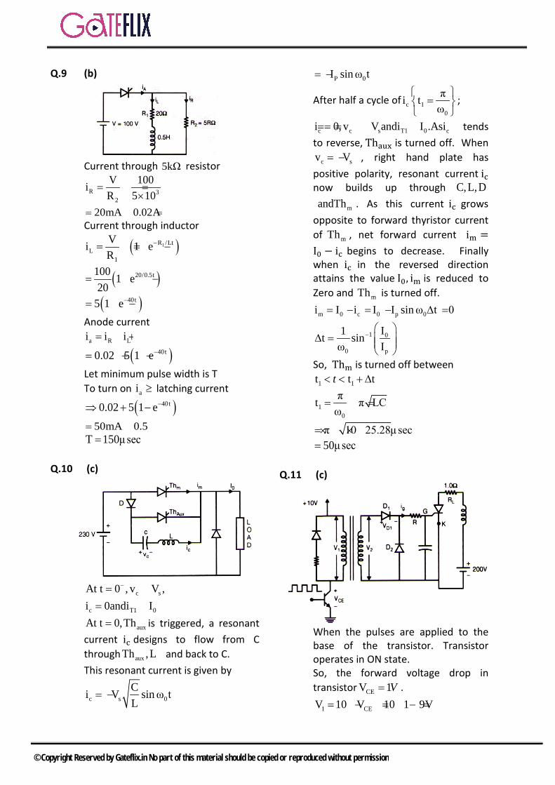
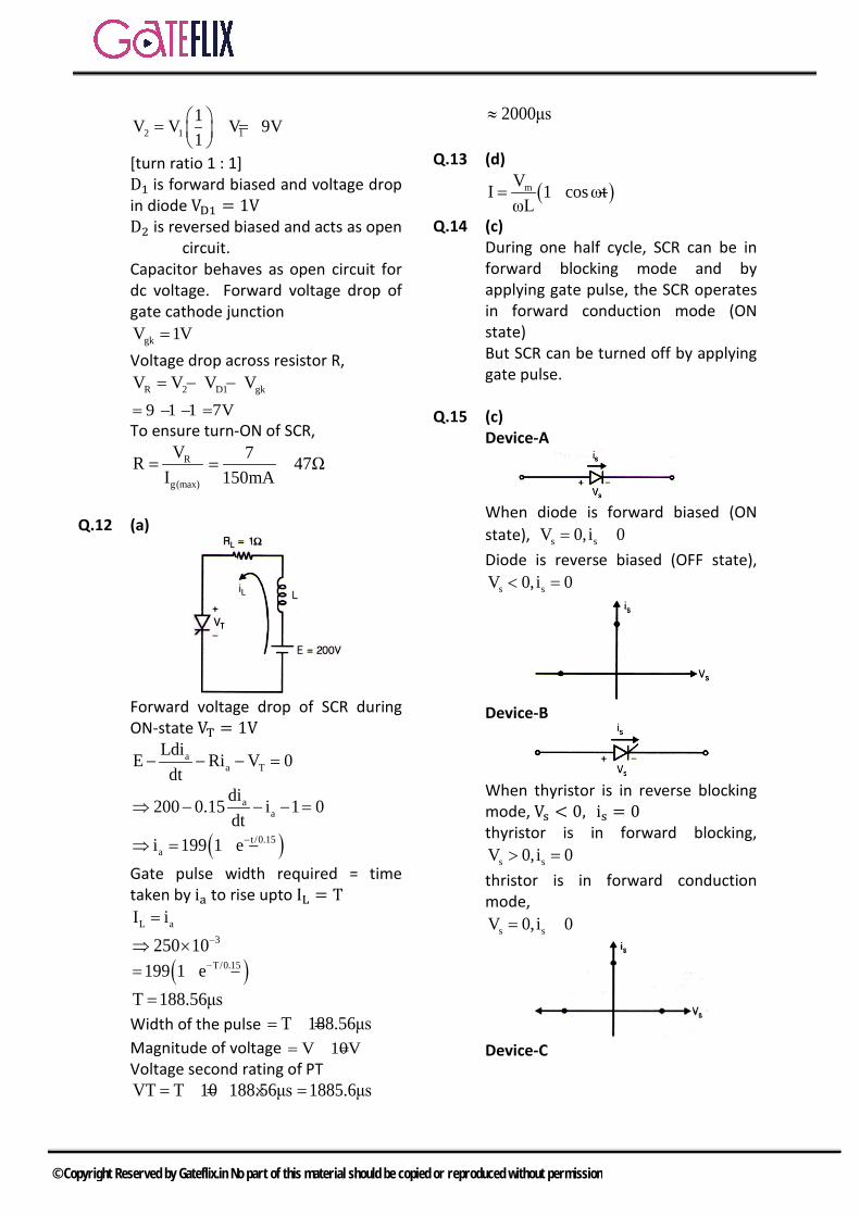
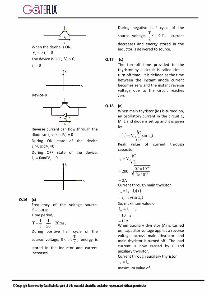
155
POWER ELECTRONICS For ELECTRICAL ENGINEERING
| Date post: | 25-Feb-2023 |
| Category: |
Documents |
| Upload: | khangminh22 |
| View: | 0 times |
| Download: | 0 times |

POWER ELECTRONICS
For ELECTRICAL ENGINEERING


SYLLABUS Characteristics of semiconductor power devices: Diode, Thyristor, Triac, GTO, MOSFET, IGBT; DC to DC conversion: Buck, Boost and Buck-Boost converters; Single and three phase configuration of uncontrolled rectifiers, Line commutated thyristor based converters, Bidirectional ac to dc voltage source converters, Issues of line current harmonics, Power factor, Distortion factor of ac to dc converters, Single phase and three phase inverters, Sinusoidal pulse width modulation.
ANALYSIS OF GATE PAPERS
Exam Year 1 Mark Ques. 2 Mark Ques. Total 2003 3 4 11 2004 4 6 16 2005 3 5 13 2006 1 8 17 2007 4 7 18 2008 2 6 14 2009 1 4 9 2010 2 - 2 2011 2 3 8 2012 2 3 8 2013 - 7 14
2014 Set-1 2 3 8 2014 Set-2 1 3 7 2014 Set-3 - 3 6 2015 Set-1 2 3 8 2015 Set-2 2 3 8 2016 Set-1 2 4 10 2016 Set-2 3 4 11 2017 Set-1 2 2 6 2017 Set-2 4 3 10
2018 4 2 8
POWER ELECTRONICS
© Copyright Reserved by Gateflix.in No part of this material should be copied or reproduced without permission
Topics Page No
1. POWER SEMICONDUCTOR DEVICES
1.1 Introduction 01 1.2 Diodes & Transistors 02 1.3 Thyristors 05 1.4 Uni-junction Transistor (UJT) 14 1.5 Comparison between GTO and Thyristor 15 1.6 Comparison between Transistors & Thyristors 16 1.7 Types of Thyristors 16 1.8 Gate/Base Commutating Devices 19
Gate Question 25
2. PHASE CONTROLLED RECTIFIERS
2.1 1- Half Wave Rectifier 39 2.2 1- Full Wave Bridge Converter 41 2.3 3 - Converter 43 2.4 Dual Converter 44 2.5 Performance Parameters 45
Gate Question 51
3. CHOPPERS
3.1 Introduction 72 3.2 Step-Up Choppers 73 3.3 Types of Chopper Circuits 74 3.4 Commutation 77
Gate Question 83
4. INVERTERS
4.1 Introduction 96 4.2 Single Phase Bridge Inverter 96 4.3 3- Bridge Inverter 98 4.4 PWM Inverters 100
Gate Question 103
5. ELECTRICAL DRIVERS
5.1 Introduction 116
5.2 Types of SMPS 117
CONTENTS
© Copyright Reserved by Gateflix.in No part of this material should be copied or reproduced without permission
5.3 Uninterruptible Power Supplies 120 5.4 Cycloconverter Introduction 120 5.5 Single-Phase to Single-Phase Circuit-Step-Up Cycloconverter 121 5.6 Three-Phase Half-Wave Cycloconverters 124 5.7 AC Voltage Controller 125 5.8 Comparision between Cycloconverter And D.C. Link Converter 127
Gate Question 128
6. ASSIGNMENT QUESTIONS 132
© Copyright Reserved by Gateflix.in No part of this material should be copied or reproduced without permission
1.1 INTRODUCTION
Power electronics is a branch of engineering that combines the fields of electrical power, electronics, and control. It started with the introduction of the mercury are rectifier in 1900. The grid controlled vacuum tube rectifier, ignitron, and thyratron followed later. These found extensive application in industrial power control till 1950. In the meanwhile the invention of the transistor – a semiconductor device- in 1948 marked a revolution in the field of electronics. It also paved the way for the introduction of the silicon controlled rectifier (SCR), which was announced in 1957 by the General Electric Company. In due course it has come to be named as the ‘thyristor’.
1.1.1 ADVANTAGES OF POWER ELECTRONIC
1. High efficiency because of low ‘ON state’conduction losses when the powersemiconductor is conducting and low‘OFF state’ leakage when it is blockingthe source voltage
2. Reduced maintenance3. Long life4. Compactness because of the facility of
assembling the thyristors, diodes, andRLC elements in a common package
5. Faster dynamic response as comparedto electromechanical equipment
6. Lower acoustic noise as compared toelectromagnetic controllers.
1.1.2 DISADVANTAGES
1. They generate harmonics whichadversely affect the loads connected tothem and also get injected into thesupply lines
2. Controlled rectifiers operate at lowpower factors and cause derating of theassociated rectifier transformers
3. They do not have a short-time overloadcapacity. However, as their advantagesoutnumber their demerits, they arewidely used in the various applicationsdetailed above. They have also replacedconventional controllers.
1.1.3 APPLICATIONS OF POWER ELECTRONICS
1. Aerospace: Space shuttle powersupplies, satellite power supplies,aircraft power systems.
2. Commercial: Advertising, heating, airconditioning, central refrigeration,computer and office equipment,uninterruptible power supplies,elevators, light dimmers and flashers.
3. Industrial: Arc and industrial furnaces,blowers & fans, pumps & compressors,industrial lasers, transformer-tapchangers, rolling mills, textile mills,excavators, cement mills, welding.
4. Residential: Air conditioning, cooking,lighting, space heating, refrigerators,electric-door openers, dryers, fans,personal computers, otherentertainment equipment, vacuumcleaners, washing and sewing machines,light dimmers, food mixers, electricblankets, food-warmer trays.
5. Telecommunication: Battery chargers,power supplies (dc and UPS)
6. Transportation: Battery chargers,traction control of electric vehicles,electric locomotives, street cars, trolleybuses, subways and automotiveelectronics.
7. Utility systems: High voltage dctransmission (HVDC), excitationsystems VAR compensation, static
1 POWER SEMICONDUCTOR DEVICES
© Copyright Reserved by Gateflix.in No part of this material should be copied or reproduced without permission
circuit breakers, fans and boiler-feed pumps, supplementary energy systems (solar, wind)
1.1.4 CONTROLLED SWITCHES
Turn on and Turn off by the application of control signals. BJT, MOSFET, GTO, SITH, IGBT, SIT, MCT • SCR, GTO, SITH & MCT require pulse
gate signal for turning them on • BJT, MOSFET, IGBT, SIT require
continuous signal for keeping them in turn on state
• The devices which can with standunipolar voltage are BJT, MOSFET, IGBT, MCT
• Thyristors and GTOs are capable forsupporting bipolar voltages.
• Triac and RCT (Reverse ConductingTheory) possess bidirectional current capabilityDiode, SCR, GTO, BJT, MOSFET, IGBT, SIT, SITH, MCT are unidirectional current devices
1.2 DIODES & TRANSISTORS
1.2.1 POWER DIODES
Power semiconductors devices are more complex in structure and in operation. Low power devices must be modified in order to make them suitable for high power applications. Power diodes are constructed with n- layer called drift region, because p+
layer (anode) and n+ layer (cathode). This is done to support large blocking voltages. Power devices operate at lower switching speeds whereas signal diodes and transistors operate at higher switching speeds.
Applications: 1) As freewheeling diodes2) For recovery of trapped energy
Static Characteristic of power diodes
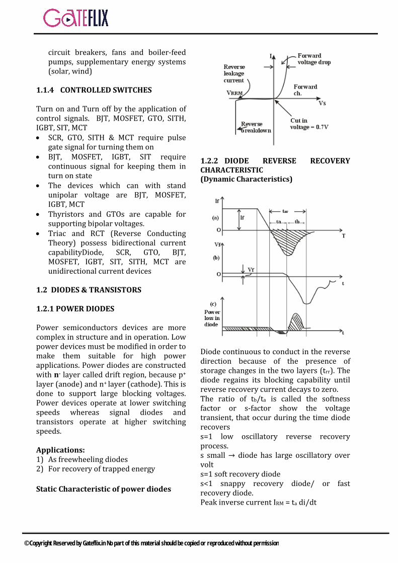
1.2.2 DIODE REVERSE RECOVERY CHARACTERISTIC (Dynamic Characteristics)
Diode continuous to conduct in the reverse direction because of the presence of storage changes in the two layers (trr). The diode regains its blocking capability until reverse recovery current decays to zero. The ratio of tb/ta is called the softness factor or s-factor show the voltage transient, that occur during the time diode recovers s=1 low oscillatory reverse recovery process. s small → diode has large oscillatory over volt s=1 soft recovery diode s<1 snappy recovery diode/ or fast recovery diode. Peak inverse current IRM = ta di/dt
© Copyright Reserved by Gateflix.in No part of this material should be copied or reproduced without permission
1.2.3 TYPES OF POWER DIODES
1. General Purpose DiodesHigher reverse recovery time trr (25 μs),Current rating1A to 1000A,Voltagerating 50V to 5KVApplications:Battery chargingElectric tractionElectro platingWeldingUPS
2. Fast recovery diodestrr = 5μs or less, Voltage : 50V to 3KVolt,1A to K amp.In order to shorten the reverserecovery time platinum or gold dopingis carried outbut this doping is carriedout → increase forward drop in diodeApplications:ChopperCommutator circuitsSwitching mode power supply (SMPS)Induction heating
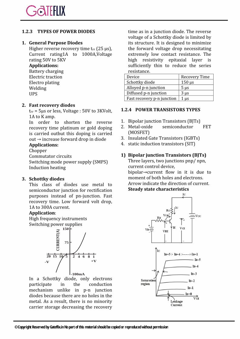
3. Schottky diodesThis class of diodes use metal tosemiconductor junction for rectificationpurposes instead of pn-junction. Fastrecovery time. Low forward volt drop,1A to 300A current.Application:High frequency instrumentsSwitching power supplies
20 15 10 5 2 4 6 8 1-V
-100mA
75
150
CURR
ENT(
A)
+V
In a Schottky diode, only electrons participate in the conduction mechanism unlike in p-n junction diodes because there are no holes in the metal. As a result, there is no minority carrier storage decreasing the recovery
time as in a junction diode. The reverse voltage of a Schottky diode is limited by its structure. It is designed to minimize the forward voltage drop necessitating extremely low contact resistance. The high resistivity epitaxial layer is sufficiently thin to reduce the series resistance.
Device Recovery Time Schottky diode 150 µs Alloyed p-n junction 5 µs Diffused p-n junction 3 µs Fast recovery p-n junction 1 µs
1.2.4 POWER TRANSISTORS TYPES
1. Bipolar junction Transistors (BJTs)2. Metal-oxide semiconductor FET
(MOSFET)3. Insulated Gate Transistors (IGBTs)4. static induction transistors (SIT)
1) Bipolar junction Transistors (BJTs)Three layers, two junctions pnp/ npn,current control device,bipolar→current flow in it is due tomoment of both holes and electrons.Arrow indicate the direction of current.Steady state characteristics
© Copyright Reserved by Gateflix.in No part of this material should be copied or reproduced without permission
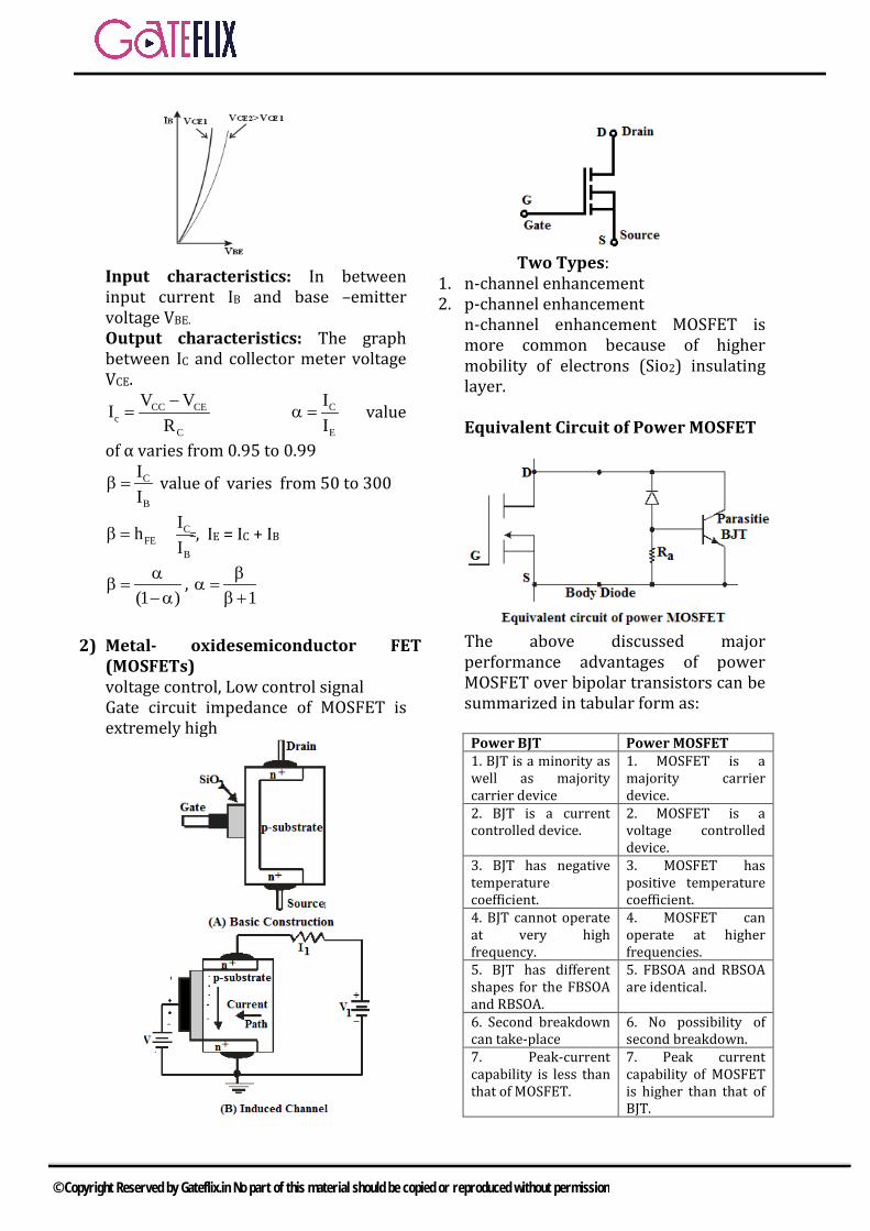
Input characteristics: In between input current IB and base –emitter voltage VBE.
Output characteristics: The graph between IC and collector meter voltage VCE.
CC CEc
C
V VIR−
= C
E
II
α = value
of α varies from 0.95 to 0.99 C
B
II
β = value of varies from 50 to 300
CFE
B
IhI
β = = , IE = IC + IB
(1 )α
β =−α
, 1
βα =
β+
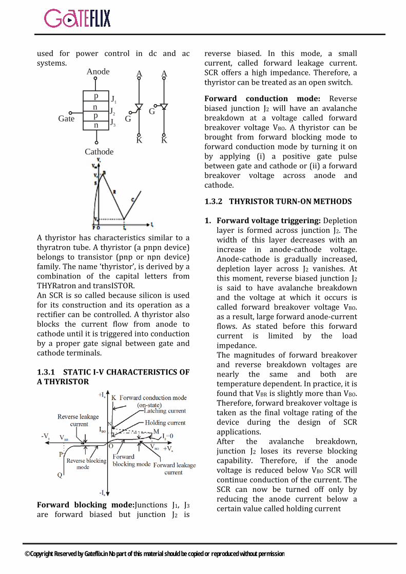
2) Metal- oxidesemiconductor FET(MOSFETs)voltage control, Low control signalGate circuit impedance of MOSFET isextremely high
Two Types: 1. n-channel enhancement2. p-channel enhancement
n-channel enhancement MOSFET ismore common because of highermobility of electrons (Sio2) insulatinglayer.
Equivalent Circuit of Power MOSFET
The above discussed major performance advantages of power MOSFET over bipolar transistors can be summarized in tabular form as:
Power BJT Power MOSFET 1. BJT is a minority aswell as majority carrier device
1. MOSFET is amajority carrier device.
2. BJT is a currentcontrolled device.
2. MOSFET is avoltage controlled device.
3. BJT has negativetemperature coefficient.
3. MOSFET haspositive temperature coefficient.
4. BJT cannot operateat very high frequency.
4. MOSFET canoperate at higher frequencies.
5. BJT has differentshapes for the FBSOA and RBSOA.
5. FBSOA and RBSOAare identical.
6. Second breakdowncan take-place
6. No possibility ofsecond breakdown.
7. Peak-currentcapability is less than that of MOSFET.
7. Peak currentcapability of MOSFET is higher than that of BJT.
© Copyright Reserved by Gateflix.in No part of this material should be copied or reproduced without permission

8. BJTs are lesssensitive to voltage spikes than MOSFETs.
8. MOSFETs are moresensitive to voltage spikes than BJT.
9. The on-statevoltage is lower than that of power-MOSFET. Therefore, the on-state loss is lower.
9. The on-statevoltage is higher than that of power BJT.
10. Conduction lossesof a BJT are less than that of MOSFET.
10. Conduction lossesof a MOSFET are greater than BJT.
11. Switching lossesare more.
11. Switching lossesare less.
12. More energyefficient at low frequency
12. More energyefficient at high frequency.
3) Insulated Gate Transistors (IGBTs):IGBT has been developed by combininginto it the best qualities of both BJT andPMOSFET. Thus an IGBT possesses highinput impedance like a PMOSFET andhas low on-state power loss as in a BJT.Further, IGBT is free from secondbreakdown problem present in BJT. Allthese merits have made IGBT verypopular amongst power-electronicsengineers.
Comparison of IGBT and MOSFET MOSFETs IGBTs 1. In the power MOSFET,the decrease in the electron mobility with increasing temperature results in a rapid increase in the on-state resistance of the channel and hence the on-state drop.
1. In IGBTs, this increasein voltage drop is very small.
2. The on-state voltagedrop increases by a factor of 3 between room temperature and 200oC
2. Here with the identicalcondition, the increment in the on-state voltage drop is very small
3. All highest temperature, maximum current rating goes down to 1/3 value.
3. At high ambienttemperature; IGBT is extraordinarily well suited.
4. Current sharing inmultiple paralleled MOSFETs is comparatively poor than IGBTs.
4. Current sharing inmultiple paralleled IGBTs is far better than power MOSFET.
5. The turn-on transients are identical
5. Turn-on transients areidentical to MOSFETs.
to IGBTs. 6. Power MOSFETs issuited for application that require low blocking voltage and high operating frequencies.
6. IGBT is the preferreddevice for applications that require high blocking voltages and lower operating frequencies.
Application of IGBTs IGBTs are widely used in medium power application such as dc and ac motor drives, UPS systems, Power supplies and drives for solenoids, relays and contactors. Though IGBTs are somewhat more expensive than BJTs, yet they are becoming popular because of lower gate-drive requirements, lower switching losses and smaller snubber circuit requirements. IGBT converters are more efficient with less size as well as cost, as compared to converters based on BJTs. Recently, IGBT iverter induction-motor drives using 15-20 kHz switching frequency are finding favour where audio-noise is objectionable. In most application, IGBTs will eventually push out BJTs. At present, the state of the art IGBTs of 1200 V, 500 A ratings 0.25 to 20 µ s turn-off time with operating frequency upto 50 KHz available.
4) PUT (Programmable UnifunctionTransistor): The characteristic of PUTand UJT are similar, the peak and valleycurrents of the PUT are typically lowerthan those of the UJT of a similar rating.
1.3 THYRISTORS
Bell Laboratories were the first to fabricate a silicon-based semiconductor device called thyristor. Semiconductor devices, with their characteristics identical with that of a thyristor, are triac, diac, silicon-controlled switch, programmable unijunction transistor (PUT), GTO, RCT etc. This whole family of semiconductor devices is given the name thyristor. Thus the term thyristor denotes a family of semiconductor devices
© Copyright Reserved by Gateflix.in No part of this material should be copied or reproduced without permission
used for power control in dc and ac systems.
J1
J2
J3
pnpn
Gate
Anode
Cathode
A
K
G
A
K
G
A thyristor has characteristics similar to a thyratron tube. A thyristor (a pnpn device) belongs to transistor (pnp or npn device) family. The name ‘thyristor’, is derived by a combination of the capital letters from THYRatron and transISTOR. An SCR is so called because silicon is used for its construction and its operation as a rectifier can be controlled. A thyristor also blocks the current flow from anode to cathode until it is triggered into conduction by a proper gate signal between gate and cathode terminals.
1.3.1 STATIC I-V CHARACTERISTICS OF A THYRISTOR
Forward blocking mode:Junctions J1, J3
are forward biased but junction J2 is
reverse biased. In this mode, a small current, called forward leakage current. SCR offers a high impedance. Therefore, a thyristor can be treated as an open switch.
Forward conduction mode: Reverse biased junction J2 will have an avalanche breakdown at a voltage called forward breakover voltage VBO. A thyristor can be brought from forward blocking mode to forward conduction mode by turning it on by applying (i) a positive gate pulse between gate and cathode or (ii) a forward breakover voltage across anode and cathode.
1.3.2 THYRISTOR TURN-ON METHODS
1. Forward voltage triggering: Depletionlayer is formed across junction J2. Thewidth of this layer decreases with anincrease in anode-cathode voltage.Anode-cathode is gradually increased,depletion layer across J2 vanishes. Atthis moment, reverse biased junction J2
is said to have avalanche breakdownand the voltage at which it occurs iscalled forward breakover voltage VBO.as a result, large forward anode-currentflows. As stated before this forwardcurrent is limited by the loadimpedance.The magnitudes of forward breakoverand reverse breakdown voltages arenearly the same and both aretemperature dependent. In practice, it isfound that VBR is slightly more than VBO.Therefore, forward breakover voltage istaken as the final voltage rating of thedevice during the design of SCRapplications.After the avalanche breakdown,junction J2 loses its reverse blockingcapability. Therefore, if the anodevoltage is reduced below VBO SCR willcontinue conduction of the current. TheSCR can now be turned off only byreducing the anode current below acertain value called holding current
© Copyright Reserved by Gateflix.in No part of this material should be copied or reproduced without permission
2. Gate Triggering: Turning on ofthyristors by gate triggering is simple,reliable and efficient; it is therefore themost usual method of firing the forwardbiased SCRs. A thyristor with forwardbreakover voltage (say 800 V) higherthan the normal working voltage (say400 V) is chosen.When positive gate current is applied,gate p layer is flooded with electronsfrom the cathode. This is becausecathode n layer is heavily doped ascompared to gate p layer. As thethyristor is forward biased, some ofthese electrons reach junction J2. As aresult, width of depletion layer nearjunction J2 is reduced. This causes thejunction J2 to breakdown at an appliedvoltage lower than the forwardbreakover voltage VBO. If magnitude ofgate current is increased, moreelectorns would reach junction J2, as aconsequence thyristor would get turnedon at a much lower forward appliedvoltage.
3. With forward voltage across theanode and cathode of a thyristor, thetwo outer junctionJ1, J3 are forwardbiased, but inner junction J2, has thecharacteristics of a capacitor due tocharges existing across the junction. Inother words, space-charges exist in thedepletion region near junction J2 andtherefore junction J2 behaves like acapacitance. If forward voltage issuddenly applied, a charging currentthrough junction capacitance Cj mayturn on the SCR.
ic =dQdt
= ddt
(Cj.Va) = Cj adVdt
+ Va. jdCdt
……..(4.1a) As the junction capacitance is almost
constant, jdCdt
is zero
iC = Cj adVdt
Therefore, if rate of rise of forward voltage dVa/dt is high, the charging current ic would be more. This charging current plays the role of gate current and turns on the SCR even though gate signal is zero.
4. Temperature Triggering (ThermalTriggering): During forward blocking,most of the applied voltage appearsacross reverse biased junction J2. Thisvoltage across, J2, associated withleakage current, would raise thetemperature of this junction. Withincrease in temperature, width ofdepletion layer decreases. This furtherleads to more leakage current andtherefore, more junction temperature.With the cumulative process, at somehigh temperature (within the safelimits), depletion layer of reversebiased junction vanishes and the devicegets turned on.
© Copyright Reserved by Gateflix.in No part of this material should be copied or reproduced without permission
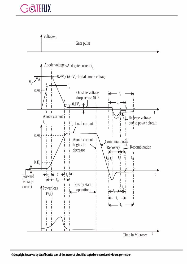
Voltage g
Gate pulse
Anode voltage And gate current i ga
VaA
0.9Va OA=V =Initial anode voltagea
Ig
0.9Ig
0.1Va
On state voltagedrop across SCR
tc
tq
tReverse voltagedue to power circuit
Anode currentia I =Load currenta
Anode currentbegins todecrease
Commutation didt
t1 t2t3
t4 t5
Recovery Recombination
tForwardleakagecurrent
0.9Ia
0.1Ia
tdtr tp
ton
Power loss (v i )a a
Steady state operation
tc
tq
trr
tgr
tTime in Microsec
© Copyright Reserved by Gateflix.in No part of this material should be copied or reproduced without permission
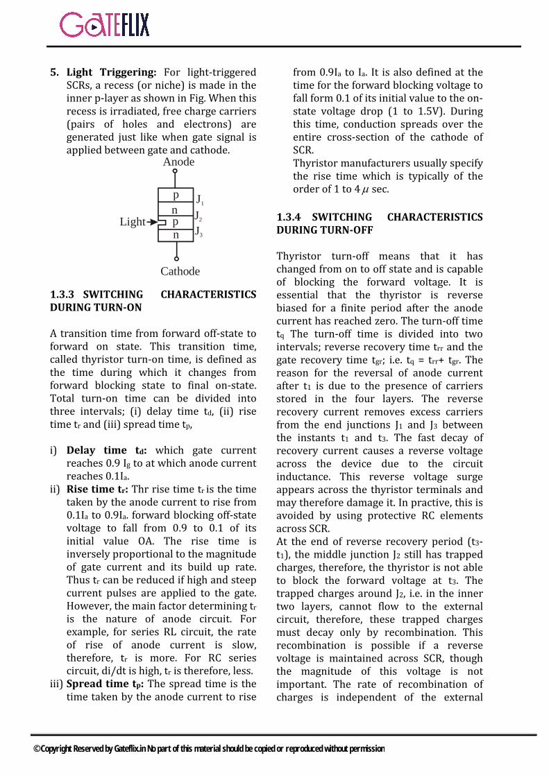
5. Light Triggering: For light-triggeredSCRs, a recess (or niche) is made in theinner p-layer as shown in Fig. When thisrecess is irradiated, free charge carriers(pairs of holes and electrons) aregenerated just like when gate signal isapplied between gate and cathode.
J1
J2
J3
pnpn
Anode
Cathode
Light
1.3.3 SWITCHING CHARACTERISTICS DURING TURN-ON
A transition time from forward off-state to forward on state. This transition time, called thyristor turn-on time, is defined as the time during which it changes from forward blocking state to final on-state. Total turn-on time can be divided into three intervals; (i) delay time td, (ii) rise time tr and (iii) spread time tp,
i) Delay time td: which gate currentreaches 0.9 Ig to at which anode currentreaches 0.1Ia.
ii) Rise time tr: Thr rise time tr is the timetaken by the anode current to rise from0.1Ia to 0.9Ia. forward blocking off-statevoltage to fall from 0.9 to 0.1 of itsinitial value OA. The rise time isinversely proportional to the magnitudeof gate current and its build up rate.Thus tr can be reduced if high and steepcurrent pulses are applied to the gate.However, the main factor determining tr
is the nature of anode circuit. Forexample, for series RL circuit, the rateof rise of anode current is slow,therefore, tr is more. For RC seriescircuit, di/dt is high, tr is therefore, less.
iii) Spread time tp: The spread time is thetime taken by the anode current to rise
from 0.9Ia to Ia. It is also defined at the time for the forward blocking voltage to fall form 0.1 of its initial value to the on-state voltage drop (1 to 1.5V). During this time, conduction spreads over the entire cross-section of the cathode of SCR. Thyristor manufacturers usually specify the rise time which is typically of the order of 1 to 4 µ sec.
1.3.4 SWITCHING CHARACTERISTICS DURING TURN-OFF
Thyristor turn-off means that it has changed from on to off state and is capable of blocking the forward voltage. It is essential that the thyristor is reverse biased for a finite period after the anode current has reached zero. The turn-off time tq The turn-off time is divided into two intervals; reverse recovery time trr and the gate recovery time tgr; i.e. tq = trr+ tgr. The reason for the reversal of anode current after t1 is due to the presence of carriers stored in the four layers. The reverse recovery current removes excess carriers from the end junctions J1 and J3 between the instants t1 and t3. The fast decay of recovery current causes a reverse voltage across the device due to the circuit inductance. This reverse voltage surge appears across the thyristor terminals and may therefore damage it. In practive, this is avoided by using protective RC elements across SCR. At the end of reverse recovery period (t3-t1), the middle junction J2 still has trapped charges, therefore, the thyristor is not able to block the forward voltage at t3. The trapped charges around J2, i.e. in the inner two layers, cannot flow to the external circuit, therefore, these trapped charges must decay only by recombination. This recombination is possible if a reverse voltage is maintained across SCR, though the magnitude of this voltage is not important. The rate of recombination of charges is independent of the external
© Copyright Reserved by Gateflix.in No part of this material should be copied or reproduced without permission
circuit parameters. The time for the recombination of charges between t3 and t4 is called gate recovery time tgr. The thyristor turn-off time tq is in the range of 3 to 100 µ sec.
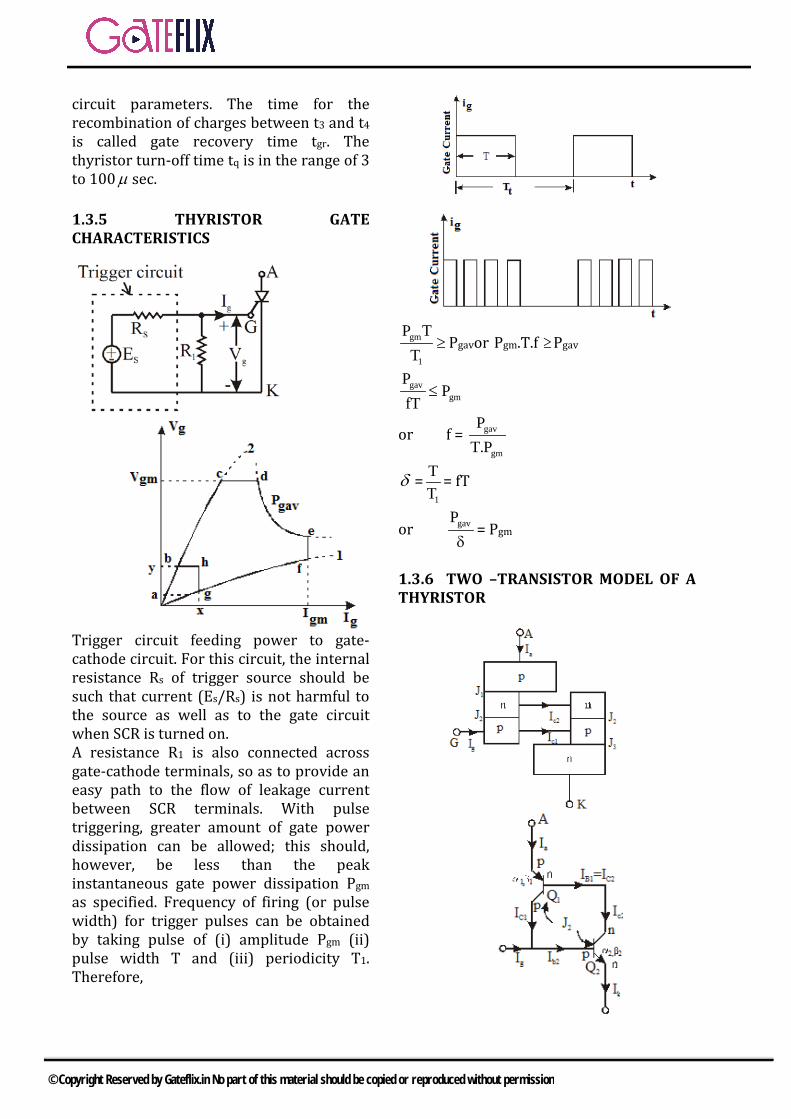
1.3.5 THYRISTOR GATE CHARACTERISTICS
Trigger circuit feeding power to gate-cathode circuit. For this circuit, the internal resistance Rs of trigger source should be such that current (Es/Rs) is not harmful to the source as well as to the gate circuit when SCR is turned on. A resistance R1 is also connected across gate-cathode terminals, so as to provide an easy path to the flow of leakage current between SCR terminals. With pulse triggering, greater amount of gate power dissipation can be allowed; this should, however, be less than the peak instantaneous gate power dissipation Pgm as specified. Frequency of firing (or pulse width) for trigger pulses can be obtained by taking pulse of (i) amplitude Pgm (ii) pulse width T and (iii) periodicity T1. Therefore,
gm
1
P TT
≥ Pgavor Pgm.T.f ≥Pgav
gavgm
PP
fT≤
or f = gav
gm
PT.P
δ =1
TT
= fT
or gavPδ
= Pgm
1.3.6 TWO –TRANSISTOR MODEL OF A THYRISTOR
© Copyright Reserved by Gateflix.in No part of this material should be copied or reproduced without permission
Ia = 2 g CBO1 CBO2
1 2
I I I1 ( )
α + +
− α +αSCR derating below dc value =
Idc - dcIFF
=Idc11
FF −
1.3.7 SURGE CURRENT RATING
A surge current rating indicates the maximum possible non-repetitive, or surge, current which the device can withstand. This rating is specified in terms of the number of surge cycles with corresponding surge current peak. Surge current rating in inversely proportional to the duration of the surge. It is usual to measure the surge duration in terms of the number of cycles of normal power frequency of 50 or 60 Hz. For example, a three-cycle surge current rating for a period of 60 msec (3×20 msec) for 50 Hz supply consists of three conducting half-cycles, each followed by an off-period. One cycle surge current rating is the peak value of allowable non-recurrent half-sine wave of 10 msec duration for 50 Hz. For duration less than half-cycle i.e. 10 msec, a subcycle surge current rating is also specified.
I 2sb .t = I2.T Isb = I T
twhere T = time for one half-cycle of supply frequency, sec I = one-cycle surge current rating, A Isb= subcycle surge current rating, A t = duration of subcycle surge, sec For 50 Hz supply, T = 10 msec
∴ Isb = I10
. 1t
1.3.8 THYRISTOR PROTECTION
a) di/dt protection: If the rate of anodecurrent, i.e.dt/dt, is large as comparedto the spread velocity of carriers, localhot spots will be formed near the gateconnection on account of high current
density. This localized heating may destroy the thyristor. The value of di/dt can be maintained below acceptable limit by using a small inductor, called di/dt inductor. Typical di/dt limit values of SCRs are 20-500 A/ µ sec.
b) dv/dt protection: If rate of rise ofsuddenly applied voltage acrossthyristor is high, the device may getturned on. dVa/dt must be kept belowthe specified rated limit. Typical valuesof dv/dt are 20-500 V/ µ sec.
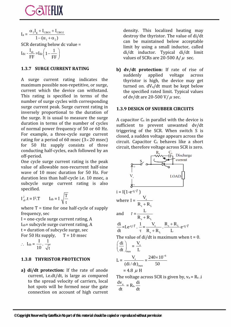
1.3.9 DESIGN OF SNUBBER CIRCUITS
A capacitor Cs in parallel with the device is sufficient to prevent unwanted dv/dt triggering of the SCR. When switch S is closed, a sudden voltage appears across the circuit. Capacitor Cs behaves like a short circuit, therefore voltage across SCR is zero.
i = I(1-e-t/τ )
where I = s
s L
VR R+
and τ =s L
LR R+
didt
=I.e-t/τ . 1τ
= s
s L
VR R+
. s LR RL+ e-t/τ
The value of di/dt is maximum when t = 0.
max
didt
= sVL
L = s
max
V(di / dt)
=6240 10
50
−×
= 4.8 µ H The voltage across SCR is given by, va = Rs .i
advdt
= Rs.didt
© Copyright Reserved by Gateflix.in No part of this material should be copied or reproduced without permission
a
max
dvdt
= Rs.max
didt
a
max
dvdt
= s sR .VL
or Rs = s
LV
a
max
dvdt
= 4.8240
×300 = 6 Ω
Rs = 2ξs
LC
∴Cs = 2
s
2R
ξ
L
= 22 0.65
6× ×
4.8 ×10-6 = 0.2253 µ F
1.3.10 OVERVOLTAGE PROTECTION
i) Internal overvoltages. Large voltagesmay be generated internally during thecommutation of a thyristor. Afterthyristor anode current reduces to zero,anode current reverses due to storedcharges. This reverse recovery currentrises to a peak value at which time theSCR begins to block. After this peak,reverse recovery current decaysabruptly with large di/dt. Because ofthe series inductance L of the SCRcircuit, large transient voltage L (di/dt)is produced.
ii) External overvoltages. External overvoltages are caused due to theinterruption of current flow in aninductive circuit. The effect ofovervoltages is usually minimized byusing RC circuits & non-linear resistorscalled voltage clamping devices.
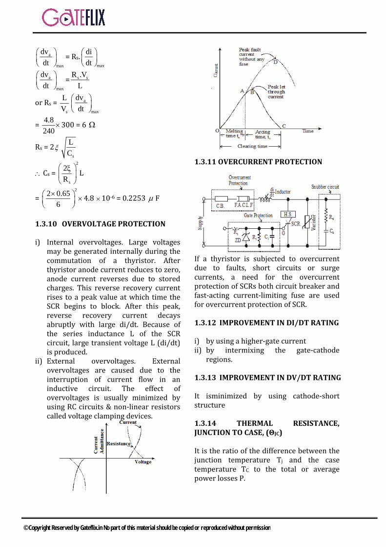
1.3.11 OVERCURRENT PROTECTION
If a thyristor is subjected to overcurrent due to faults, short circuits or surge currents, a need for the overcurrent protection of SCRs both circuit breaker and fast-acting current-limiting fuse are used for overcurrent protection of SCR.
1.3.12 IMPROVEMENT IN DI/DT RATING
i) by using a higher-gate currentii) by intermixing the gate-cathode
regions.
1.3.13 IMPROVEMENT IN DV/DT RATING
It isminimized by using cathode-short structure
1.3.14 THERMAL RESISTANCE, JUNCTION TO CASE, (ΘJC)
It is the ratio of the difference between the junction temperature Tj and the case temperature TC to the total or average power losses P.
© Copyright Reserved by Gateflix.in No part of this material should be copied or reproduced without permission
j c 0JC
T TC / W
P−
θ =
1.3.15 THERMAL RESISTANCE, HEAT SINK TO COOLING MEDIUM, (ΘSA)
It is the ratio of the difference between the sink temperature TS and cooling-medium temperature TA to the total power losses P
0S ASA
T T C / WP−
θ =
1.3.16 NONREPETITIVE SURGE CURRENT RATING
Surge current is assumed to be imposed on the device when it is operating at maximum rated voltage, current and temperature condition in a half-wave circuit delivering a resistance load. During this brief period, the forward blocking capability of the device is lost until the device is cooled down to or below the maximum rated operating temperature. This surge current is not a regular feature of the device and occurs during severe fault condition and these ratings provide the instantaneous overload capacity of the device and are used to design the protective devices for it. These ratings are generally provided in terms of nonrecurring surge current with respect to time duration of occurrence and I2t. The maximum surge current rating is provided for a minimum time duration of one half-cycle of the supply frequency, i.e. 10 m s;
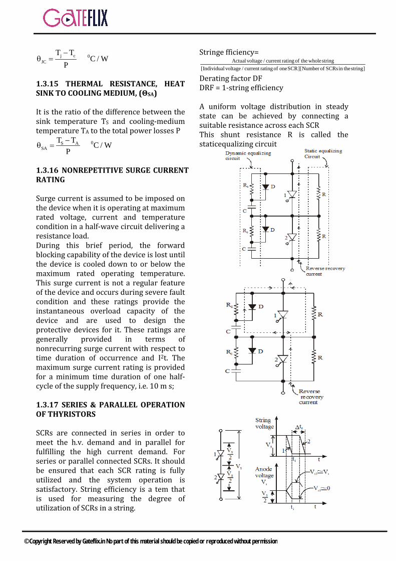
1.3.17 SERIES & PARALLEL OPERATION OF THYRISTORS
SCRs are connected in series in order to meet the h.v. demand and in parallel for fulfilling the high current demand. For series or parallel connected SCRs. It should be ensured that each SCR rating is fully utilized and the system operation is satisfactory. String efficiency is a tem that is used for measuring the degree of utilization of SCRs in a string.
Stringe fficiency= Actual voltage / current rating of the wholestring
[Individual voltage / current rating of oneSCR][Number of SCRsin thestring]
Derating factor DF DRF = 1-string efficiency
A uniform voltage distribution in steady state can be achieved by connecting a suitable resistance across each SCR This shunt resistance R is called the staticequalizing circuit
© Copyright Reserved by Gateflix.in No part of this material should be copied or reproduced without permission
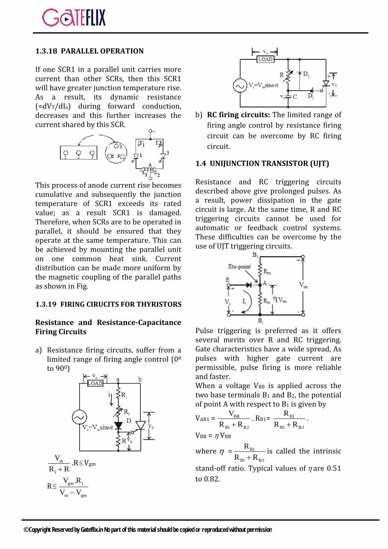
1.3.18 PARALLEL OPERATION
If one SCR1 in a parallel unit carries more current than other SCRs, then this SCR1 will have greater junction temperature rise. As a result, its dynamic resistance (=dVT/dIa) during forward conduction, decreases and this further increases the current shared by this SCR.
This process of anode current rise becomes cumulative and subsequently the junction temperature of SCR1 exceeds its rated value; as a result SCR1 is damaged. Therefore, when SCRs are to be operated in parallel, it should be ensured that they operate at the same temperature. This can be achieved by mounting the parallel unit on one common heat sink. Current distribution can be made more uniform by the magnetic coupling of the parallel paths as shown in Fig.
1.3.19 FIRING CIRUCITS FOR THYRISTORS
Resistance and Resistance-Capacitance Firing Circuits
a) Resistance firing circuits, suffer from alimited range of firing angle control (00
to 900)
m
1
VR R+
.R≤Vgm
R≤ gm 1
m gm
V .RV V−
b) RC firing circuits: The limited range offiring angle control by resistance firingcircuit can be overcome by RC firingcircuit.
1.4 UNIJUNCTION TRANSISTOR (UJT)
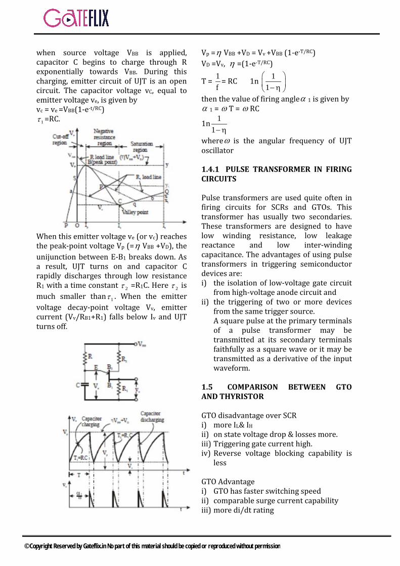
Resistance and RC triggering circuits described above give prolonged pulses. As a result, power dissipation in the gate circuit is large. At the same time, R and RC triggering circuits cannot be used for automatic or feedback control systems. These difficulties can be overcome by the use of UJT triggering circuits.
Pulse triggering is preferred as it offers several merits over R and RC triggering. Gate characteristics have a wide spread, As pulses with higher gate current are permissible, pulse firing is more reliable and faster. When a voltage VBB is applied across the two base terminals B1 and B2, the potential of point A with respect to B1 is given by
VAB1 = BB
B1 B2
VR R+
. RB1= B1
B1 B2
RR R+
.
VBB = ηVBB
where η = B1
B1 B2
RR R+
is called the intrinsic
stand-off ratio. Typical values of η are 0.51 to 0.82.
© Copyright Reserved by Gateflix.in No part of this material should be copied or reproduced without permission
when source voltage VBB is applied, capacitor C begins to charge through R exponentially towards VBB. During this charging, emitter circuit of UJT is an open circuit. The capacitor voltage vC, equal to emitter voltage ve, is given by vc = ve =VBB(1-e-t/RC)
1τ =RC.
When this emitter voltage ve (or vc) reaches the peak-point voltage Vp (=η VBB +VD), the unijunction between E-B1 breaks down. As a result, UJT turns on and capacitor C rapidly discharges through low resistance R1 with a time constant 2τ =R1C. Here 2τ is much smaller than 1τ . When the emitter voltage decay-point voltage Vv, emitter current (Vv/RB1+R1) falls below Iv and UJT turns off.
Vp =η VBB +VD = Vv +VBB (1-e-T/RC) VD =Vv, η =(1-e-T/RC)
T = 1f
= RC 1n 11 −η
then the value of firing angleα 1 is given by α 1 = ω T = ω RC
1n 11−η
whereω is the angular frequency of UJT oscillator
1.4.1 PULSE TRANSFORMER IN FIRING CIRCUITS
Pulse transformers are used quite often in firing circuits for SCRs and GTOs. This transformer has usually two secondaries. These transformers are designed to have low winding resistance, low leakage reactance and low inter-winding capacitance. The advantages of using pulse transformers in triggering semiconductor devices are: i) the isolation of low-voltage gate circuit
from high-voltage anode circuit and ii) the triggering of two or more devices
from the same trigger source. A square pulse at the primary terminals of a pulse transformer may be transmitted at its secondary terminals faithfully as a square wave or it may be transmitted as a derivative of the input waveform.
1.5 COMPARISON BETWEEN GTO AND THYRISTOR
GTO disadvantage over SCR i) more IL& IH
ii) on state voltage drop & losses more.iii) Triggering gate current high.iv) Reverse voltage blocking capability is
less
GTO Advantage i) GTO has faster switching speedii) comparable surge current capabilityiii) more di/dt rating
© Copyright Reserved by Gateflix.in No part of this material should be copied or reproduced without permission
iv) GTO circuit has lower size and weightv) GTO has higher efficiencyvi) GTO unit has reduced acoustical and
electromagnetic noise due toelimination of commutation chokes.
1.6 COMPARISON BETWEEN TRANSISTORS & THYRISTORS
Transistors Thyristors (1) Transistor is a three-layer, two junction device.
(1) Thyristor is a four layer, three junction device.
(2) To keep a transistor in the conducting state, a continuous base current is required.
(2) Thyristors require a pulse to make it conducting and thereafter it remain conducting
(3) When transistor (power transistor) conduct appreciable current, the forward voltage drop is of the order of 0.3 to 0.8 V.
(3) The forward voltage drop across the device is of the order of 1.2 to 2V.
(4) The voltage and current ratings of transistors available at present are not as high as those of thyristors.
(4) Due to the difference in fabrication and operation, thyristors with very high voltage and current ratings are available.
(5) Power transistors have no surge current capacity and can withstand only a low rate change of current.
(5) Thyristors have surge-current rating and therefore can withstand high rate of change of current compared to transistors.
(6) Commutation circuitry, which is costly and bulky, is not required.
(6) Commutation circuit is required.
(7) Power transistors switch on faster than SCRs, and turn-off problems are practically non existent. If the base current is removed, the transistor turns of f. Therefore, power-transistors can be used in very high-frequency applications.
(7) Thyristors are used in comparatively low frequency applications.
(8) Circuits using power transistors will be smaller in size and less costly compared to circuits using thyristors.
(8) Comparatively larger in size and is costlier.
(9) There has been little operating experience in
(9) Thyristor circuits, on the other
high power application of transistors. Power transistors or Darlington pairs are more susceptible to failure.
hand, have a proven record of many years of reliable operation.
Modern era of solid-state power-electronics began with the advent of thyristor (silicon controlled rectifier) in the late 1950’s. Gradually, other devices such as traic (1958), gate-turn-off thyristor (GTO-1958), bipolar transistor (IGBT-1985), static induction transistor (SIT-1975) and integrated gate commtated thyristor (IGCT-1987) were introduced. The BJT appeared and then fell into obsolescence due to the advent of IGBT at the higher end and power MOSFET at the lower-end. The invention of IGBTs is an important milestone in the history of power-semiconductor devices. Commercial IGBTs are available with 3.5 kV, 1.2 kA, but upto 6.5 kVand 10 kV devices are under test in laboratory. Trench gate IGBT with reduced conduction drop is available up to 1.2 kV, 600 A. IGBT intelligent power modules (IPM) from number of vendors are available for 600 A. 50-300 A and 1200 V, 50-150 A to cover upto hp ac drive applications. IGCT (also called GCT) is basically a hard-drived GTO with built-in gate driver, and device is available with 6 kV, 6 kA (10 kV device, are under test). ABB introduced recently a reverse blocking IGCT (6 kV, 800 A) for use in current-fed inverter drives.
1.7 TYPES OF THYRISTORS
i) Phase-Control Thyristorsii) Inverter-Grade Thyristors (fast-
switchingSCRs)iii) Asymmetrical-Thyristors (ASCRs)iv) Reverse-conducting Thyristors (RCTs)v) Gate-Assisted Turn-off Thyristors
(GATTs)vi) Bidirectional Diode Thyristors (DIACs)vii) Bidirectional Triode Thyristors (Triacs)viii) Silicon Unilateral Switch (SUS)ix) Silicon Bilateral Switch (SBS)
© Copyright Reserved by Gateflix.in No part of this material should be copied or reproduced without permission
x) Silicon-Controlled Switch (SCS)xi) Light-Activated silicon Controlled
Rectifiers(LASCRs)
In general, the turn-on operation of the devices of this type is controllable using a trigger signal. However, the turn-off operaion depends upon the condition of the power circuit. Hence, in this type, only turn-on switching is externally controllable.
1.7.1 INVERTER-GRADE THYRISTORS
The most common feature of an inverter-grade thyristor which distinguishes it from a standard phase control type is that it has fast turn-off time, generally in the range of 5 to 50 µs, depending upon voltage rating. Therefore, these are used high-speed switching applications with forced commutation. Inverter thyristors are generally used in circuits that operate from d.c. supplies where current in the thyristor is turned off either through the use of auxiliary commutating circuitry, by circuit resonance, or by “load” commutation. Whatever be the circuit turn-off mechanism, fast turn-off is important because it minimizes size and weight of commutating and/or reactive circuit components.
These thyristors have high dv/dt of typically 1000 V/µs and di/dt of 1000 A/µs. The fast turn off and high di/dt are very important to reduce the size and weight of commutating and/or reactive circuit components. The conduction voltage of a 2200 A, 1800 V thyristor is typically 1.7 V. The conventional thyristor may have a reverse blocking capability of thousands of
volts, but this capability is not required for every application. In particular, the voltage-fed inverter circuit, which converts d.c. power to a.c., usually has rectifier diode connected in antiparallel across each thyristor to conduct reactive load currents and excess commutating current. In such circuits, the antiparallel diode clamps the thyristor reverse voltage to 1 or 2 V under steady circuits conditions. One of the main characteristics of an asymmetrical thyristor (ASCR) is that they do not block significant reverse voltage. Therefore, an ASCR is specifically, the reverse voltage rating is about 20 or 30 V and the forward voltage rating is of the range 400-2000 V. The switching times and on-state voltage drop of an ASCR are smaller than those of a conventional thyristor of the same rating. As already indicated, a fast turn off is important because it minimizes the size, weight and cost of commutating circuit components, and permits operation at switching frequencies of 20 kHz, or more with high-efficiency.
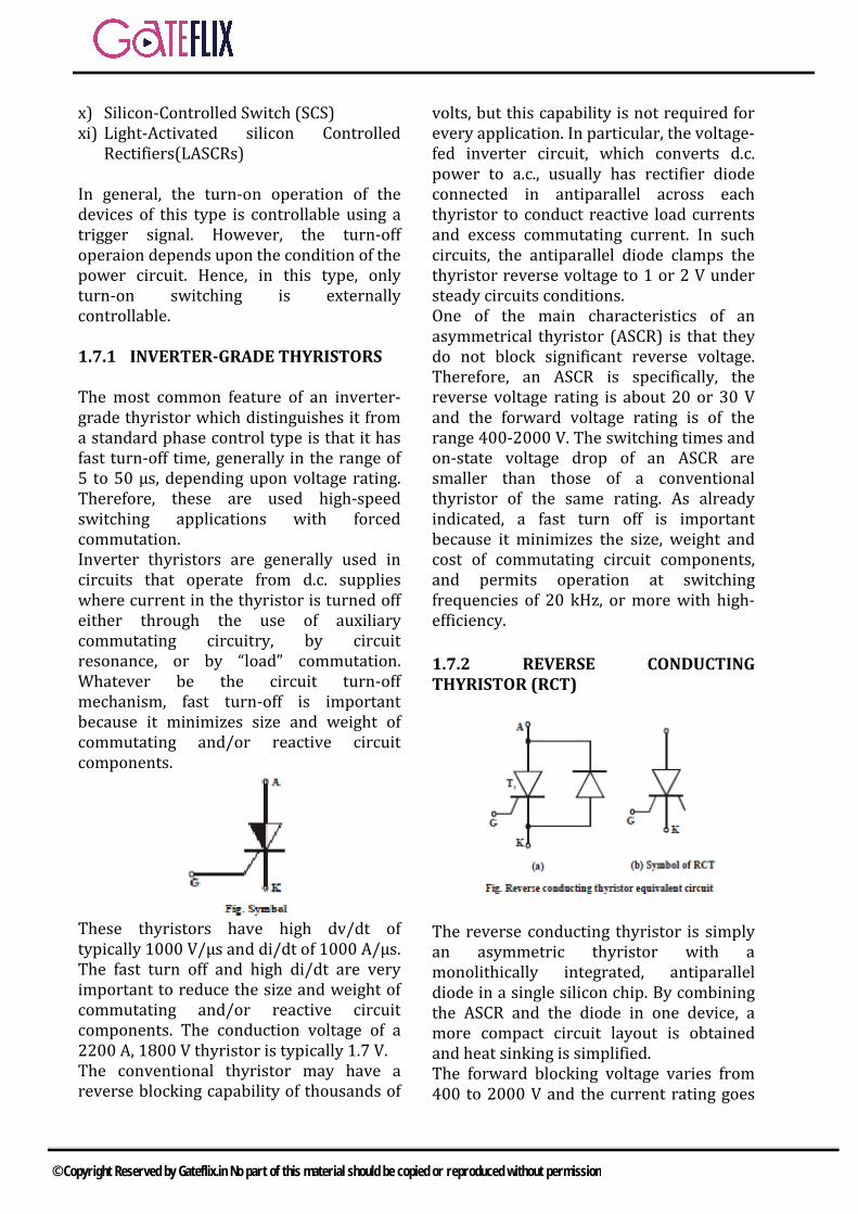
1.7.2 REVERSE CONDUCTING THYRISTOR (RCT)
The reverse conducting thyristor is simply an asymmetric thyristor with a monolithically integrated, antiparallel diode in a single silicon chip. By combining the ASCR and the diode in one device, a more compact circuit layout is obtained and heat sinking is simplified. The forward blocking voltage varies from 400 to 2000 V and the current rating goes
© Copyright Reserved by Gateflix.in No part of this material should be copied or reproduced without permission
upto 500 A. The reverse blocking voltage is typically 30 to 40 V. A disadvantage of the RCT is that it is inflexible compared with two discrete devices. In the voltage source inverter, the load current is controlled by the thyristor and flows freely in the other direction through the diode. For such circuits, the RCT must have equal current ratings for thyristor and diode sections. Purpose designed RCT devices are now being manufactured for high performance inverter and chopper circuits.
1.7.3 BIDIRECTIONAL DIODE THYRISTOR (DIAC)
A Diac is a two electrode, bidirectional avalanche diode which can be switched from the off-state to the on-state for either polarity of applied voltage. Conduction occurs in the Diac when the breakover voltage is reached in either polarity across the two terminals. Diac is mainly used as a trigger device for Triacs which require either positive or negative gate pulses to turn ON. In fact, matched Diac-Triac pairs are available in the market for various types of control circuits.
1.7.4 BIDIRECTIONAL TRIODE THYRISTOR (TRIAC)
Because of the interaction between the two halves of the device, Triacs are limited in voltage, current, and frequency ratings as compared with conventional thyristors. The Triac finds widespread use in consumer and light indudtrial appliances operating from 50 or 60 Hz a.c. supplies at moderate power levels. The plastic encapsulated Triac is a particularly cheap and compact device and is widely used for controlling the speed single-phase a.c. series or universal motors, in such consumer appliances as food mixers and portable drills.
Advantages of Triac
1. Triacs can be triggered with positive ornegative polarity voltages.
2. A Triac needs a single heat sink ofslightly larger size, whereas antiparallelthyristor pair needs two heat sinks ofslightly smaller sizes, but due to theclearance total space required is morefor thyristors.
3. A Triac needs a single fuse forprotection, which also simplifiesconstruction.
4. In some d.c. applications, SCR isrequired to be connected with a paralleldiode to protect against reverse voltage,whereas a Triac used may work withouta diode, as safe breakdown in eitherdirection is possible.
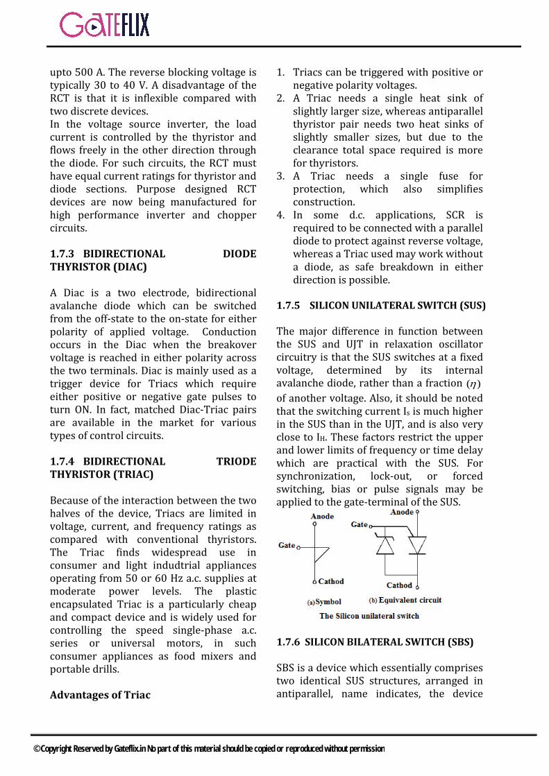
1.7.5 SILICON UNILATERAL SWITCH (SUS)
The major difference in function between the SUS and UJT in relaxation oscillator circuitry is that the SUS switches at a fixed voltage, determined by its internal avalanche diode, rather than a fraction )(ηof another voltage. Also, it should be noted that the switching current Is is much higher in the SUS than in the UJT, and is also very close to IH. These factors restrict the upper and lower limits of frequency or time delay which are practical with the SUS. For synchronization, lock-out, or forced switching, bias or pulse signals may be applied to the gate-terminal of the SUS.
1.7.6 SILICON BILATERAL SWITCH (SBS)
SBS is a device which essentially comprises two identical SUS structures, arranged in antiparallel, name indicates, the device
© Copyright Reserved by Gateflix.in No part of this material should be copied or reproduced without permission
conducts in both directions when the applied voltage breaks the internal avalanche diode.
Fig (a).(b) Silicon Bilateral switch
1.7.7 SILICON CONTROLLED SWITCH (SCS)
The additional lead is connected to the N region below the anode P region. SCS has two gates, one anode gate like a PUT and another cathode gate like and SCR, as shown in Fig. The SCS can be turned-off in any of the three ways: 1) By reducing its anode current below IH
(same as SCR),2) By applying a negative pulse at Gk,3) By applying a positive pulse at GA.
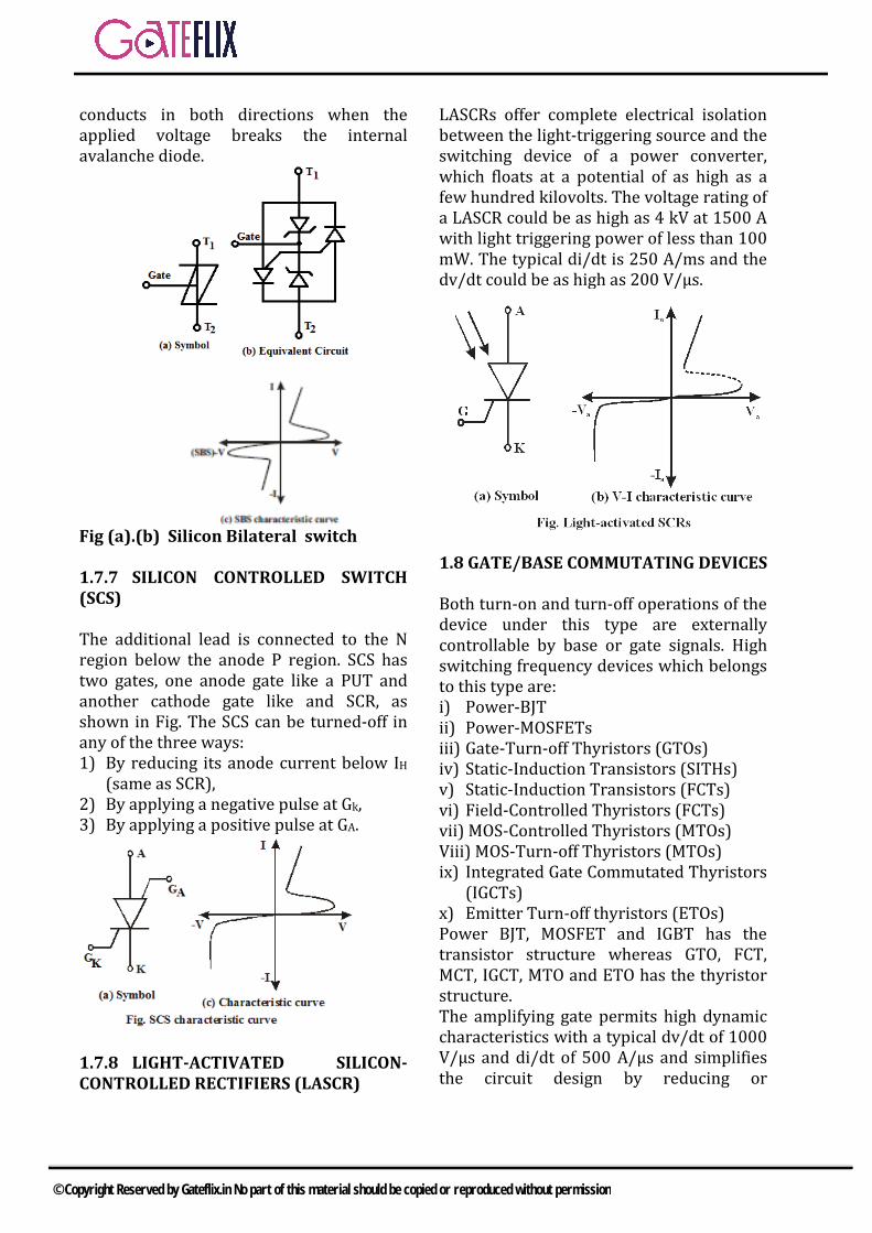
1.7.8 LIGHT-ACTIVATED SILICON-CONTROLLED RECTIFIERS (LASCR)
LASCRs offer complete electrical isolation between the light-triggering source and the switching device of a power converter, which floats at a potential of as high as a few hundred kilovolts. The voltage rating of a LASCR could be as high as 4 kV at 1500 A with light triggering power of less than 100 mW. The typical di/dt is 250 A/ms and the dv/dt could be as high as 200 V/µs.
1.8 GATE/BASE COMMUTATING DEVICES
Both turn-on and turn-off operations of the device under this type are externally controllable by base or gate signals. High switching frequency devices which belongs to this type are: i) Power-BJTii) Power-MOSFETsiii) Gate-Turn-off Thyristors (GTOs)iv) Static-Induction Transistors (SITHs)v) Static-Induction Transistors (FCTs)vi) Field-Controlled Thyristors (FCTs)vii) MOS-Controlled Thyristors (MTOs)Viii) MOS-Turn-off Thyristors (MTOs) ix) Integrated Gate Commutated Thyristors
(IGCTs)x) Emitter Turn-off thyristors (ETOs)Power BJT, MOSFET and IGBT has the transistor structure whereas GTO, FCT, MCT, IGCT, MTO and ETO has the thyristor structure. The amplifying gate permits high dynamic characteristics with a typical dv/dt of 1000 V/µs and di/dt of 500 A/µs and simplifies the circuit design by reducing or
© Copyright Reserved by Gateflix.in No part of this material should be copied or reproduced without permission
minimizing dv/dt protection circuits di/dt limiting inductor.
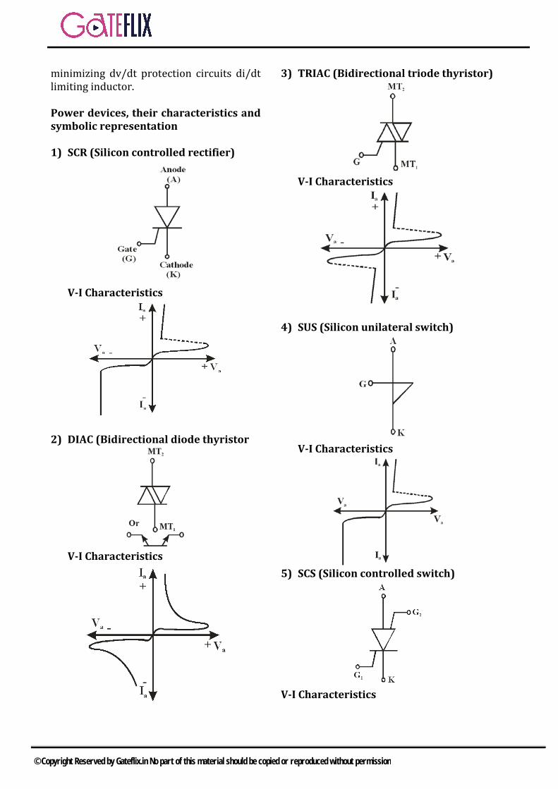
Power devices, their characteristics and symbolic representation
1) SCR (Silicon controlled rectifier)
V-I Characteristics
2) DIAC (Bidirectional diode thyristor
V-I Characteristics
3) TRIAC (Bidirectional triode thyristor)
V-I Characteristics
4) SUS (Silicon unilateral switch)
V-I Characteristics
5) SCS (Silicon controlled switch)
V-I Characteristics
© Copyright Reserved by Gateflix.in No part of this material should be copied or reproduced without permission
6) SBS (Silicon bilateral switch)
V-I Characteristics
7) LASCR (Light activated SCR)
V-I Characteristics
8) LASCS (Light activated SCS)
V-I Characteristics
9) PUT (Programmable unijunctiontransistor)
V-I Characteristics
10) RCT (Reverse conducting thyristor)
Ia
Va
Va
Ia
Ia
Va
Va
Ia
Ia
Va
Va
Ia
© Copyright Reserved by Gateflix.in No part of this material should be copied or reproduced without permission
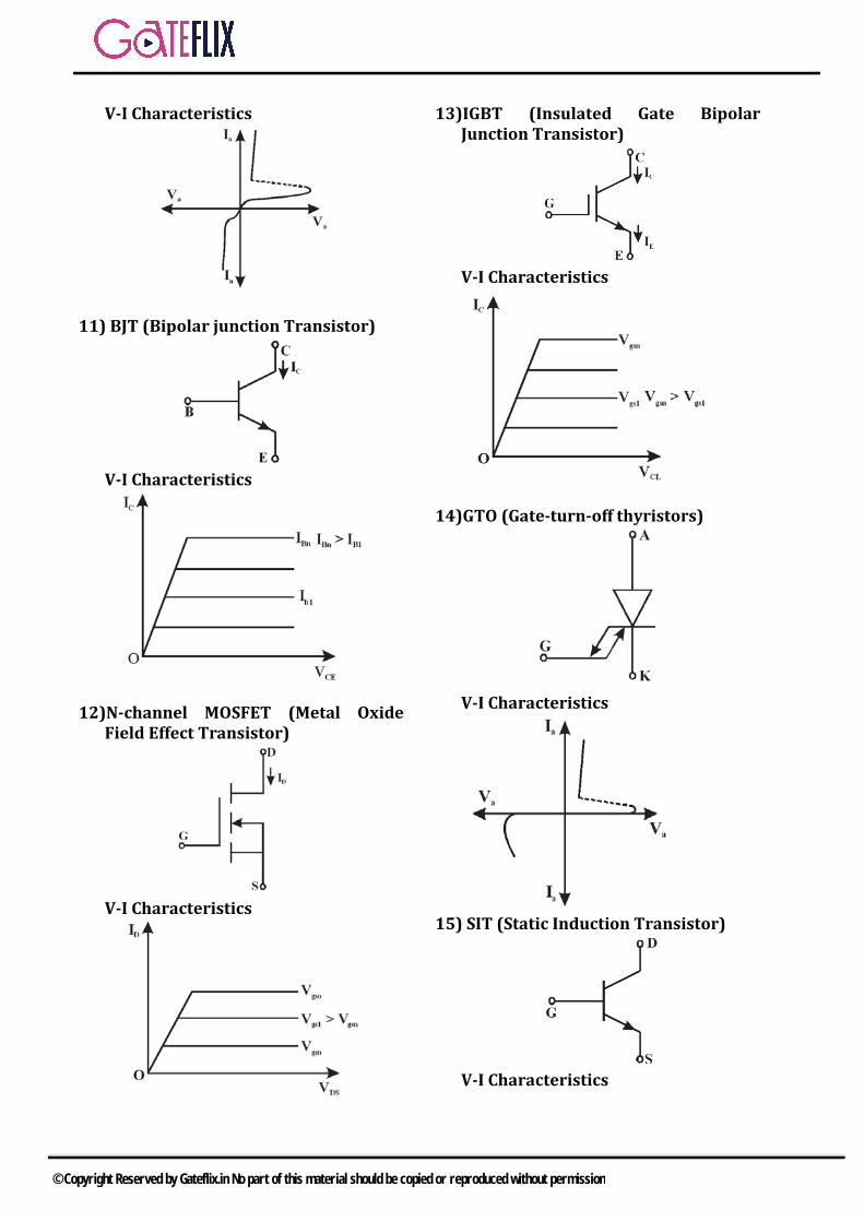
V-I Characteristics
11) BJT (Bipolar junction Transistor)
V-I Characteristics
12)N-channel MOSFET (Metal OxideField Effect Transistor)
V-I Characteristics
13)IGBT (Insulated Gate BipolarJunction Transistor)
V-I Characteristics
14)GTO (Gate-turn-off thyristors)
V-I Characteristics
15) SIT (Static Induction Transistor)
V-I Characteristics
© Copyright Reserved by Gateflix.in No part of this material should be copied or reproduced without permission
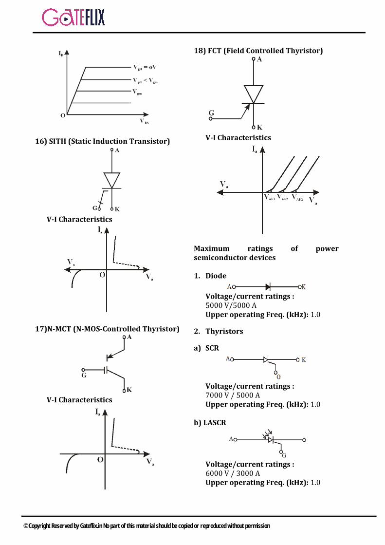
16) SITH (Static Induction Transistor)
V-I Characteristics
17)N-MCT (N-MOS-Controlled Thyristor)
V-I Characteristics
18) FCT (Field Controlled Thyristor)
V-I Characteristics
Maximum ratings of power semiconductor devices
1. Diode
Voltage/current ratings : 5000 V/5000 A Upper operating Freq. (kHz): 1.0
2. Thyristors
a) SCR
Voltage/current ratings : 7000 V / 5000 A Upper operating Freq. (kHz): 1.0
b) LASCR
Voltage/current ratings : 6000 V / 3000 A Upper operating Freq. (kHz): 1.0
© Copyright Reserved by Gateflix.in No part of this material should be copied or reproduced without permission
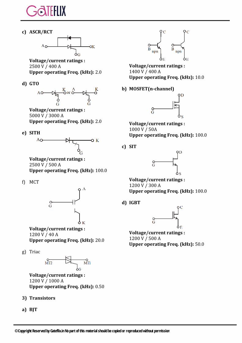
c) ASCR/RCT
Voltage/current ratings : 2500 V / 400 A Upper operating Freq. (kHz): 2.0
d) GTO
Voltage/current ratings : 5000 V / 3000 A Upper operating Freq. (kHz): 2.0
e) SITH
Voltage/current ratings : 2500 V / 500 A Upper operating Freq. (kHz): 100.0
f) MCT
Voltage/current ratings : 1200 V / 40 A Upper operating Freq. (kHz): 20.0
g) Triac
Voltage/current ratings : 1200 V / 1000 A Upper operating Freq. (kHz): 0.50
3) Transistors
a) BJT
Voltage/current ratings : 1400 V / 400 A Upper operating Freq. (kHz): 10.0
b) MOSFET(n-channel)
Voltage/current ratings : 1000 V / 50A Upper operating Freq. (kHz): 100.0
c) SIT
Voltage/current ratings : 1200 V / 300 A Upper operating Freq. (kHz): 100.0
d) IGBT
Voltage/current ratings : 1200 V / 500 A Upper operating Freq. (kHz): 50.0
© Copyright Reserved by Gateflix.in No part of this material should be copied or reproduced without permission
Q.1 Figure shows MOSFET with an integral body diode. It is employed as a power switching device in the ON and OFF states through appropriate control. The ON and OFF states of the switch are given on the DS sV I− plane by
a) b)
c) d) [GATE-2003]
Q.2 Figure shows a thyristor with the standard terminations of anode (A), cathode (K), gate (G) and the different junctions named J1, J2 and J3. When the thyristor is turned on and conducting
a) J1 and J2 are forward biased andJ3 is reverse biased
b) J1 and J3 are forward biased andJ2 is reverse biased
c) J1 is forward biased and J2 and J3are reverse biased
d) J, J2 and J3 are all forward biased [GATE-2003]
Q.3 A bipolar junction transistor (BJT) is used as a power control switch by biasing it in the cut-off region (OFF state) or in the saturation region (ON state). In the ON state, for the BJT a) both the base-emitter and base-
collector junctions are reversebiased
b) the base-emitter junction isreverse biased, and the base-collector junction is forwardbiased
c) the base -emitter junction isforward biased, and the base-collector junction is reverse biased
d) both the base-emitter and base-collector junctions are forwardbiased
[GATE-2004]
Q.4 A MOSFFET rated for 10A carries a periodic current as shown in figure. The ON state resistance of the MOSFET is 0 15Ω. . The average ON state loss in the MOSET is
a) 33.8 W b) 15.0 Wc) 7.5 W d) 3.8 W
[GATE-2004]
Q.5 The conduction loss versus device current characteristic of a power MOSFET is best approximated by a) a parabolab) a straight linec) a rectangular hyperbolad) an exponentially decaying
function [GATE-2005]
GATE QUESTIONS
© Copyright Reserved by Gateflix.in No part of this material should be copied or reproduced without permission
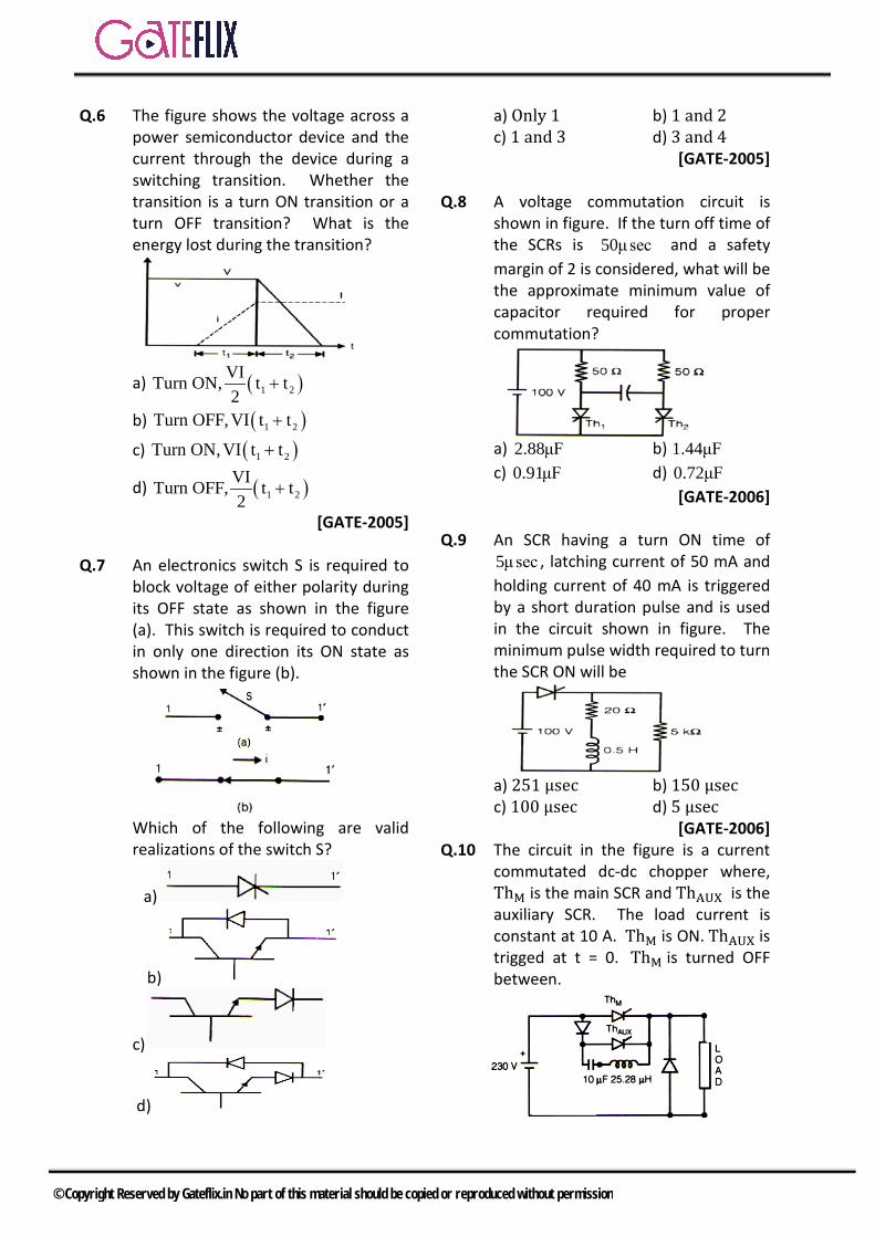
Q.6 The figure shows the voltage across a power semiconductor device and the current through the device during a switching transition. Whether the transition is a turn ON transition or a turn OFF transition? What is the energy lost during the transition?
a) ( )1 2VITurn ON, t t2
+
b) ( )1 2Turn OFF, VI t t+
c) ( )1 2Turn ON,VI t t+
d) ( )1 2VITurn OFF, t t2
+
[GATE-2005]
Q.7 An electronics switch S is required to block voltage of either polarity during its OFF state as shown in the figure (a). This switch is required to conduct in only one direction its ON state as shown in the figure (b).
Which of the following are valid realizations of the switch S?
a)
b)
c)
d)
a) Only 1 b) 1 and 2c) 1 and 3 d) 3 and 4
[GATE-2005]
Q.8 A voltage commutation circuit is shown in figure. If the turn off time of the SCRs is 50μsec and a safety margin of 2 is considered, what will be the approximate minimum value of capacitor required for proper commutation?
a) 2.88μF b) 1.44μFc) 0.91μF d) 0.72μF
[GATE-2006]
Q.9 An SCR having a turn ON time of5μsec , latching current of 50 mA and holding current of 40 mA is triggered by a short duration pulse and is used in the circuit shown in figure. The minimum pulse width required to turn the SCR ON will be
a) 251 µsec b) 150 µsecc) 100 µsec d) 5 µsec
[GATE-2006] Q.10 The circuit in the figure is a current
commutated dc-dc chopper where, ThM is the main SCR and ThAUX is the auxiliary SCR. The load current is constant at 10 A. ThM is ON. ThAUX is trigged at t = 0. ThM is turned OFF between.
© Copyright Reserved by Gateflix.in No part of this material should be copied or reproduced without permission
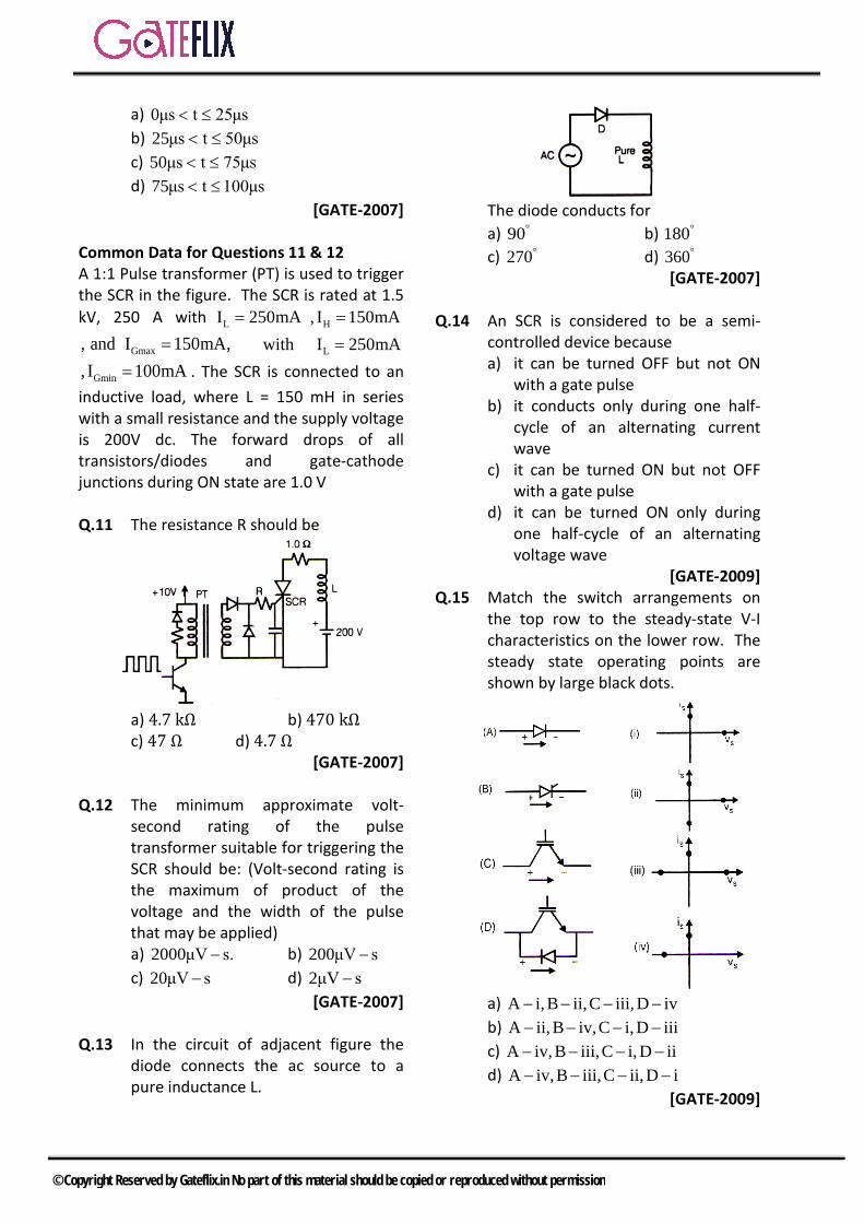
a) 0μs t 25μs< ≤b) 25μs t 50μs< ≤c) 50μs t 75μs< ≤d) 75μs t 100μs< ≤
[GATE-2007]
Common Data for Questions 11 & 12 A 1:1 Pulse transformer (PT) is used to trigger the SCR in the figure. The SCR is rated at 1.5 kV, 250 A with LI 250mA= H, I 150mA=
Gmax, and I 150mA,= Lwith I 250mA=
Gmin, I 100mA= . The SCR is connected to an inductive load, where L = 150 mH in series with a small resistance and the supply voltage is 200V dc. The forward drops of all transistors/diodes and gate-cathode junctions during ON state are 1.0 V
Q.11 The resistance R should be
a) 4.7 kΩ b) 470 kΩc) 47 Ω d) 4.7 Ω
[GATE-2007]
Q.12 The minimum approximate volt-second rating of the pulse transformer suitable for triggering the SCR should be: (Volt-second rating is the maximum of product of the voltage and the width of the pulse that may be applied) a) 2000μV s.− b) 200μV s−c) 20μV s− d) 2μV s−
[GATE-2007]
Q.13 In the circuit of adjacent figure the diode connects the ac source to a pure inductance L.
The diode conducts for a) °90 b) °180c) °270 d) °360
[GATE-2007]
Q.14 An SCR is considered to be a semi- controlled device because
a) it can be turned OFF but not ONwith a gate pulse
b) it conducts only during one half-cycle of an alternating currentwave
c) it can be turned ON but not OFFwith a gate pulse
d) it can be turned ON only duringone half-cycle of an alternatingvoltage wave
[GATE-2009] Q.15 Match the switch arrangements on
the top row to the steady-state V-I characteristics on the lower row. The steady state operating points are shown by large black dots.
a) A i,B ii,C iii,D iv− − − −b) A ii,B iv,C i,D iii− − − −c) A iv,B iii,C i,D ii− − − −d) A iv,B iii,C ii,D i− − − −
[GATE-2009]
© Copyright Reserved by Gateflix.in No part of this material should be copied or reproduced without permission
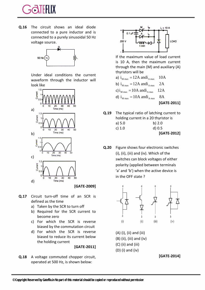
Q.16 The circuit shows an ideal diode connected to a pure inductor and is connected to a purely sinusoidal 50 Hz voltage source.
Under ideal conditions the current waveform through the inductor will look like
a)
b)
c)
d) [GATE-2009]
Q.17 Circuit turn-off time of an SCR is defined as the time a) Taken by the SCR to turn offb) Required for the SCR current to
become zeroc) For which the SCR is reverse
biased by the commutation circuitd) For which the SCR is reverse
biased to reduce its current belowthe holding current
[GATE-2011]
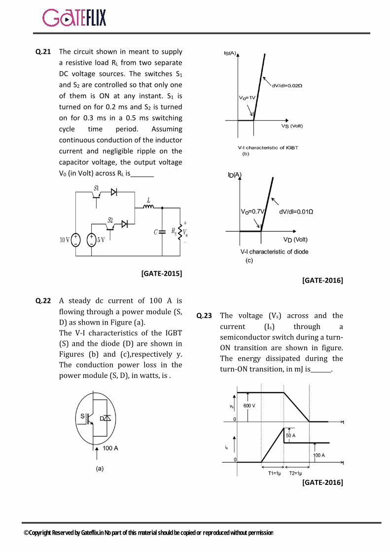
Q.18 A voltage commuted chopper circuit, operated at 500 Hz, is shown below:
If the maximum value of load current is 10 A, then the maximum current through the main (M) and auxiliary (A) thyristors will be a) M max A maxi 12A andi 10A= =b) M max A maxi 12A andi 2A= = c) M max A maxi 10A andi 12A= =d) M max A maxi 10A andi 8A= =
[GATE-2011]
Q.19 The typical ratio of latching current to holding current in a 20 thyristor is a) 5.0 b) 2.0c) 1.0 d) 0.5
[GATE-2012]
Q.20 Figure shows four electronic switches (i), (ii), (iii) and (iv). Which of the switches can block voltages of either polarity (applied between terminals ‘a’ and ‘b’) when the active device is in the OFF state ?
(A) (i), (ii) and (iii) (B) (ii), (iii) and (iv) (C) (ii) and (iii) (D) (i) and (iv)
[GATE-2014]
© Copyright Reserved by Gateflix.in No part of this material should be copied or reproduced without permission
Q.21 The circuit shown in meant to supply a resistive load RL from two separate DC voltage sources. The switches S1 and S2 are controlled so that only one of them is ON at any instant. S1 is turned on for 0.2 ms and S2 is turned on for 0.3 ms in a 0.5 ms switching cycle time period. Assuming continuous conduction of the inductor current and negligible ripple on the capacitor voltage, the output voltage V0 (in Volt) across RL is______
[GATE-2015]
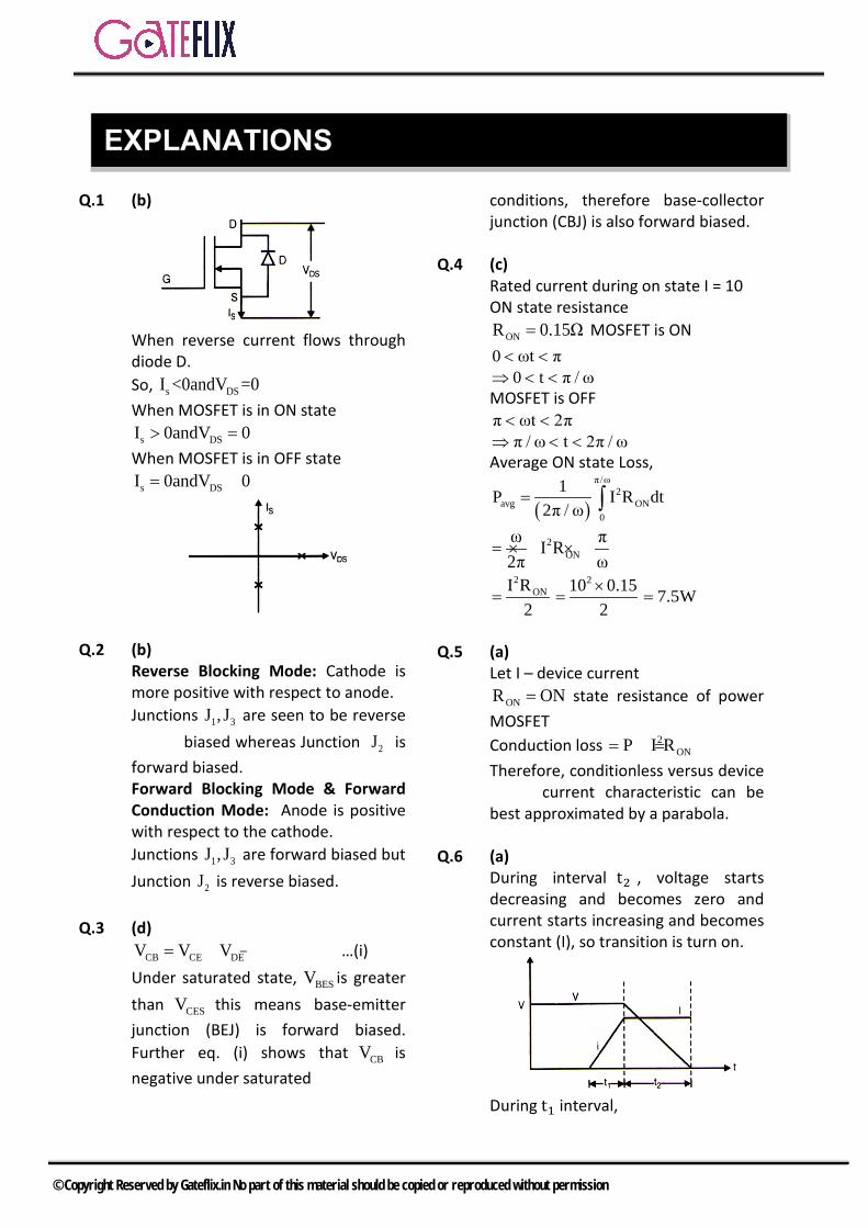
Q.22 A steady dc current of 100 A is flowing through a power module (S, D) as shown in Figure (a).The V-I characteristics of the IGBT (S) and the diode (D) are shown in Figures (b) and (c),respectively y. The conduction power loss in the power module (S, D), in watts, is .
[GATE-2016]
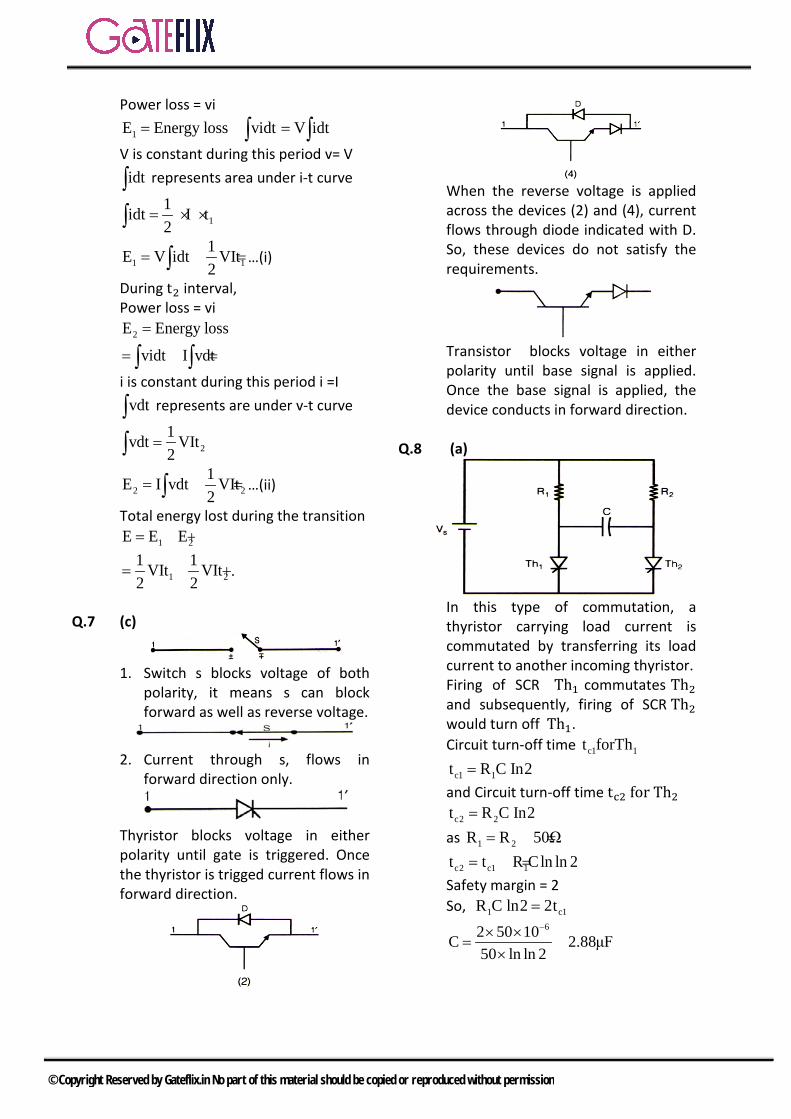
Q.23 The voltage (Vs) across and the current (Is) through a semiconductor switch during a turn-ON transition are shown in figure. The energy dissipated during the turn-ON transition, in mJ is_______.
[GATE-2016]
© Copyright Reserved by Gateflix.in No part of this material should be copied or reproduced without permission

Q.24 For the power semiconductor devices IGBT, MOSFET, Diode and Thyristor, which one of the following statement is TRUE? (A) All the four are majority carrier devices. (B) All the four are minority carrier devices. (C) IGBT and MOSFET are majority carrier devices, whereas Diode and Thyristor and minority carrier devices. (D) MOSFET is majority carrier device, whereas IGBT, Diode and Thyristor are minority carrier devices.
[GATE-2017]
Q.25 Four power semiconductor devices are shown in the figure along with their relevant terminals. The device (s) that can carry dc current continuously in the direction shown when gated appropriately is (are)
(A) Triac only (B) Triac and MOSFET (C) Triac and GTO (D) Thyristor and triac
[GATE-2018]
1 2 3 4 5 6 7 8 9 10 11 12 13 14 (b) (b) (d) (c) (a) (a) (c) (a) (b) (c) (c) (a) (d) (c) 15 16 17 18 19 20 21 22 23 24 25 (c) (c) (c) (a) (b) (c) 7 170 75 (d) (b)
ANSWER KEY:
© Copyright Reserved by Gateflix.in No part of this material should be copied or reproduced without permission
Q.1 (b)
When reverse current flows through diode D. So, s DSI <0andV =0 When MOSFET is in ON state
s DSI 0andV 0> =When MOSFET is in OFF state
s DSI 0andV 0= >
Q.2 (b) Reverse Blocking Mode: Cathode is more positive with respect to anode. Junctions 1 3J , J are seen to be reverse
biased whereas Junction 2J is forward biased. Forward Blocking Mode & Forward Conduction Mode: Anode is positive with respect to the cathode. Junctions 1 3J , J are forward biased but Junction 2J is reverse biased.
Q.3 (d) CB CE DEV V V= − …(i)
Under saturated state, BESV is greater than CESV this means base-emitter junction (BEJ) is forward biased. Further eq. (i) shows that CBV is negative under saturated
conditions, therefore base-collector junction (CBJ) is also forward biased.
Q.4 (c) Rated current during on state I = 10 ON state resistance
ONR 0.15Ω= MOSFET is ON 0 ωt π< <
0 t π / ω⇒ < <MOSFET is OFF π ωt 2π< <
π / ω t 2π / ω⇒ < <Average ON state Loss,
( )π/ω
2avg O
0N
1P I R dt2π / ω
= ∫
2ON
ω πI R2π ω
= × ×
2ONI R
2=
210 0.152×
= 7.5W=
Q.5 (a) Let I – device current
ONR ON= state resistance of power MOSFET Conduction loss 2
ONP I R= =Therefore, conditionless versus device
current characteristic can be best approximated by a parabola.
Q.6 (a) During interval t2 , voltage starts decreasing and becomes zero and current starts increasing and becomes constant (I), so transition is turn on.
During t1 interval,
EXPLANATIONS
© Copyright Reserved by Gateflix.in No part of this material should be copied or reproduced without permission
Power loss = vi
1E Energy loss vidt= = ∫ V idt= ∫V is constant during this period v= V
idt∫ represents area under i-t curve
11idt I t2
= × ×∫
1 11E V idt VIt2
= =∫ …(i)
During t2 interval, Power loss = vi
2E Energy loss=
vidt I vdt= =∫ ∫i is constant during this period i =I
vdt∫ represents are under v-t curve
21vdt VIt2
=∫
2 21E I vdt VIt2
= =∫ …(ii)
Total energy lost during the transition 1 2E E E= +
1 21 1VIt VIt2 2
= + .
Q.7 (c)
1. Switch s blocks voltage of bothpolarity, it means s can blockforward as well as reverse voltage.
2. Current through s, flows inforward direction only.
Thyristor blocks voltage in either polarity until gate is triggered. Once the thyristor is trigged current flows in forward direction.
When the reverse voltage is applied across the devices (2) and (4), current flows through diode indicated with D. So, these devices do not satisfy the requirements.
Transistor blocks voltage in either polarity until base signal is applied. Once the base signal is applied, the device conducts in forward direction.
Q.8 (a)
In this type of commutation, a thyristor carrying load current is commutated by transferring its load current to another incoming thyristor. Firing of SCR Th1 commutates Th2 and subsequently, firing of SCR Th2 would turn off Th1. Circuit turn-off time c1 1t forTh
c1 1t R C In2= and Circuit turn-off time tc2 for Th2
c2 2t R C In2= as 1 2R R 50Ω= =
c2 c1 1t t R Cln ln 2= = Safety margin = 2 So, 1 c1R C ln2 2t=
62 50 10C 2.88μF50 ln ln 2
−× ×= =
×
© Copyright Reserved by Gateflix.in No part of this material should be copied or reproduced without permission
Q.9 (b)
Current through 5kΩ resistor
R 32
V 100iR 5 10
= =×
20mA 0.02A= = Current through inductor
( )1R /LtL
1
Vi 1 eR
−= = −
( )20/0.5t100 1 e20
= −
( )40t5 1 e−= −
Anode current a R Li i i= +
( )40t0.02 5 1 e−= + −
Let minimum pulse width is T To turn on ai ≥ latching current
( )40t0.02 5 1 e−⇒ + −
50mA 0.5= = T 150μsec=
Q.10 (c)
c sAt t 0 , v V ,−= =
c T1 0i 0andi I= =
auxAt t 0,Th= is triggered, a resonant current ic designs to flow from C through auxTh ,L and back to C. This resonant current is given by
c s 0Ci V sinω tL
= −
P 0I sinω t= −
After half a cycle of c 10
πi tω
=
;
c c s T1 0 ci 0, v V andi I .Asi= = − = tends to reverse, Thaux is turned off. When
c sv V= − , right hand plate has positive polarity, resonant current ic now builds up through C,L,D
m andTh . As this current ic grows opposite to forward thyristor current of mTh , net forward current im =I0 − ic begins to decrease. Finally when ic in the reversed direction attains the value I0, im is reduced to Zero and mTh is turned off.
m 0 c 0 p 0i I i I I sinω t 0= − = − =∆
1 0
0 p
I1t sinω I
−
∆ =
So, Thm is turned off between 1 1t t t< < + ∆t
10
πt π LCω
= =
π 10 25.28μ sec= × × 50μsec=
Q.11 (c)
When the pulses are applied to the base of the transistor. Transistor operates in ON state. So, the forward voltage drop in transistor CEV 1= V .
1 CEV 10 V 10 1 9V= − = − =
© Copyright Reserved by Gateflix.in No part of this material should be copied or reproduced without permission
2 1 11V V V 9V1 = = =
[turn ratio 1 : 1] D1 is forward biased and voltage drop in diode VD1 = 1V D2 is reversed biased and acts as open
circuit. Capacitor behaves as open circuit for dc voltage. Forward voltage drop of gate cathode junction
gkV 1V=Voltage drop across resistor R,
R 2 D1 gkV V V V= − −
9 1 1 7V= − − = To ensure turn-ON of SCR,
R
g(max)
VRI
=7 47Ω
150mA= ≈
Q.12 (a)
Forward voltage drop of SCR during ON-state VT = 1V
aa T
LdiE Ri V 0dt
− − − =
aa
di200 0.15 i 1 0dt
⇒ − − − =
( )t /0.15ai 199 1 e−⇒ = −
Gate pulse width required = time taken by ia to rise upto IL = T
L aI i= 3250 10−×⇒
( )T/0.15199 1 e−= −
T 188.56μs= Width of the pulse T 188.56μs= = Magnitude of voltage V 10V= = Voltage second rating of PT VT T 10 188.56μs= = × 1885.6μs=
2000μs≈
Q.13 (d)
( )mVI 1 cosωtωL
= −
Q.14 (c) During one half cycle, SCR can be in forward blocking mode and by applying gate pulse, the SCR operates in forward conduction mode (ON state) But SCR can be turned off by applying gate pulse.
Q.15 (c) Device-A
When diode is forward biased (ON state), s sV 0,i 0= >Diode is reverse biased (OFF state),
s sV 0,i 0< =
Device-B
When thyristor is in reverse blocking mode, Vs < 0, is = 0 thyristor is in forward blocking,
s sV 0,i 0> =thristor is in forward conduction mode,
s sV 0,i 0= >
Device-C
© Copyright Reserved by Gateflix.in No part of this material should be copied or reproduced without permission
When the device is ON, s sV 0,i 0= >
The device is OFF, sV 0,>
si 0=
Device-D
Reverse current can flow through the diode so s si 0andV 0< =During ON state of the device
s si >0andV =0 During OFF state of the device,
s si 0andV 0= =
Q.16 (c) Frequency of the voltage source, f 50Hz= Time period,
1 1T 20msf 50
= = = .
During positive half cycle of the
source voltage, T0 t2
< < , energy is
stored in the inductor and current increases.
During negative half cycle of the
source voltage, T t T2≤ ≤ , current
decreases and energy stored in the inductor is delivered to source.
Q.17 (c) The turn-off time provided to the thyristor by a circuit is called circuit turn-off time. It is defined as the time between the instant anode current becomes zero and the instant reverse voltage due to the circuit reaches zero.
Q.18 (a) When main thyristor (M) is turned on, an oscillatory current in the circuit C, M, L and diode is set up and it is given by
( )c s 0Ci t V sinω tL
=
Peak value of current through capacitor
P sCi VL
=
6
3
0.1 102001 10
−
−
×= ×
×2A=
Current through main thyristor ( )m 0 ci i i t= +
0 P 0i i sinω t= +So, maximum value of
m 0 PI i i= +10 2= + 12A=
When auxiliary thyristor (A) is turned on, capacitor voltage applies a reverse voltage across main thyristor and main thyristor is turned off. The load current is now carried by C and auxiliary thyristor. Current through auxiliary thyristor
A 0i i=maximum value of
© Copyright Reserved by Gateflix.in No part of this material should be copied or reproduced without permission
A 0i maximum value ofI 10A= = .
Q.19 (b) For medium power thyristors of rating 6A to 60 A the ratio of the latching current to holding current is 1.5 to2.
Q.20 (c) We have to check all the given switches whether it can block voltages of either polarity when the active device is in the OFF state. Switch (i):
When Va > Vb ; diode will be OFF, but the transistor is ON. When Vb > Va ; transistor is OFF, but diode will be ON. So, the switch can not block voltages of either polarity when the active device(diode or transistor) is in the OFF state.
Switch (ii) :
When Va > Vb , both diode and transistor are ON. When Vb > Va both diode and transistor are OFF. So, the switch can block voltages of either polarity when the active devices (diode and transistor) are in the OFF state.
Switch (iii):
When Va > Vb , the SCR is ON.
When Vb > Va , the SCR is OFF. So, the switch can block voltages of either polarity when the active device (SCR) is in the OFF state.
Switch (iv):
When Va > Vb , diode is OFF. When Vb > Va , SCR is OFF. So, the switch can not block voltages of either polarity when the active device (SCR or diode) is in the OFF state. Thus, the switches (ii) and (iii) only can block voltage of either polarity, when active device is OFF.
Q.21 (7)
Given that only one of the two switches is ON at any instant. For 0.2 ms, S1 is ON and for 0.3 ms S2 is ON. Here, we analyze the given circuit for the two cases:
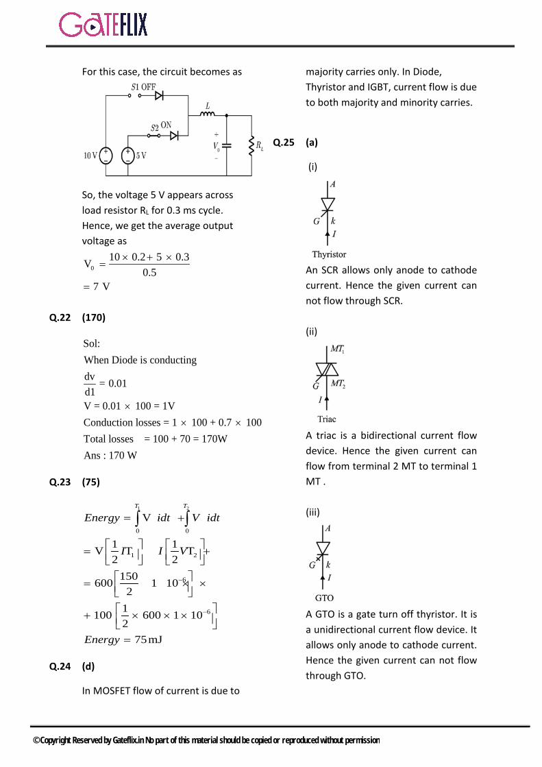
CASE 1: For 0.2 ms For this case, the circuit becomes as
So, the voltage 10 V appears across load resistor RL for 0.2 ms cycle.
CASE 2 : For 0.3 ms Cycle
© Copyright Reserved by Gateflix.in No part of this material should be copied or reproduced without permission
For this case, the circuit becomes as
So, the voltage 5 V appears across load resistor RL for 0.3 ms cycle. Hence, we get the average output voltage as
010 0.2 5 0.3V
0.57 V
× + ×=
=
Q.22 (170)
Sol:When Diode is conductingdv = 0.01d1V = 0.01 100 = 1VConduction losses = 1 100 + 0.7 100Total losses = 100 + 70 = 170WAns : 170 W
×× ×
Q.23 (75)
1 2
0 0
1 2
6
6
V
1 1V T T2 2
150600 1 102
1100 600 1 102
75mJ
T T
Energy idt V idt
I I V
Energy
−
−
= ⋅ + ⋅
= + = × × + × × × =
∫ ∫
Q.24 (d)
In MOSFET flow of current is due to
majority carries only. In Diode, Thyristor and IGBT, current flow is due to both majority and minority carries.
Q.25 (a)
(i)
An SCR allows only anode to cathode current. Hence the given current can not flow through SCR.
(ii)
A triac is a bidirectional current flow device. Hence the given current can flow from terminal 2 MT to terminal 1 MT .
(iii)
A GTO is a gate turn off thyristor. It is a unidirectional current flow device. It allows only anode to cathode current. Hence the given current can not flow through GTO.
© Copyright Reserved by Gateflix.in No part of this material should be copied or reproduced without permission

(iv)
Note : A MOSFET with body diode is a by directional current conduction device.But here the body diode is not mentioned.
The given MOSFET is a D-MOSFET. It allows only drain to source current. Hence the given current can not flow through MOSFET.
© Copyright Reserved by Gateflix.in No part of this material should be copied or reproduced without permission
2.1 1-φ HALF WAVE RECTIFIER
To discuss the rectifier action φ using Thyristor, Thyristor & Diode are considered to be ideal i.e. • Voltage drop across them is zero• No reverse current under reverse
biased conditions φ• Holding current is zero.
• In +ve half of the cycle no i0 flows SCR isfired at an angle α (firing angle) soThyristor T start conducting at θ = α. IfT were replaced by a diode then ifwould start conducting at θ = 0
• When T is conducting i.e. α<θ<π , V0 = Vs
and V0 = 0 otherwise
• As load is purely resistance so 00
ViR
=
so i0& V0 have the same waveform. • If VT is the drop across SCR,
VT = VS – V0
As V0 = sV 0 otherwise
α < θ < π
Ts
0 V
V otherwiseα < θ < π
⇒ =
• Current through thyristor iT=i0 reduceto zero at θ = ωt = π, & after θ = π, Tremains reverse biased, upto θ = wt =2π, so curriculum off time (provided bycircuit to SCR) tc given by
ωππω /=⇒= cc tt hence sufficient tc
is given so Thyristor with slow turn offtime (50-100μs) can be used ieconverter grade SCR.
• Average o/p voltage :
0 m1V V sin dv
2
π
α
= θπ ∫
mV (1 cos )2
= + απ
• V0 can be controlled by controlling ‘α’or by centralling the phase (phasedifference between i/p & o/p) hence itis called as “phase controlled Rectifier”as well as by controlling ‘α’, the actionof T as a rectifier can be controlled so itis named as (silicon controlled rectifier)
• Rms value of o/p voltage1
2 22
or 00
1V V dv2
π = π
∫12
2 2m
1 V sin d2
π
α
= θ θ π
∫
( )12
mor
V sin 2V22 zα = π−α +
• Supply current is = i0
so rms current oror
VIR
=
• Supply VA (Input VA) = Supply voltage(rms). Supply current (rms)=VS Ior
• Input power factorPower delivered to loadPF
Input VA=
( )121 sin 2PF
22α = π−α + π
2 PHASE CONTROLLED RECTIFIERS
© Copyright Reserved by Gateflix.in No part of this material should be copied or reproduced without permission
2.1.1 WITH RL-LOAD
• T starts conducting at wt = α so currenti0 state flowing from figure.
0o 0
LdiV Ridt
= +
0 slet V V when T-ON=
0m
diso L R V sin wtdt
+ =
Solution to this equation[given io = 0 at wt = α]
R (wt )m m wL
0V Vi sin (wt- )- sin( )ez Z
− −α= ϕ α −ϕ
VT = (VS – VR – VL)
as VL = 0diLdt
• Let i0 = 0 at ωt = β (extinction angle)from equation
R ( )m m wLV V0 sin( ) sin( )e
Z Z
−β−α
= β−ϕ − α −ϕ
β is given by equation β - α = γ Conduction angle
• avg V0,2
0 00
1V V d t2
π
= ωπ ∫ m
1 V sin d2
β
α
= θ θπ ∫
M0
VV [cos cos ]2
⇒ = α− βπ
• rms load voltage12
2or 0
1V V d2
β
α
= θ π
∫
12
mor
V 1V ( ) sin 2 sin 222
⇒ = β−α − β− α π
2.1.2 WITH FREEWHEELING DIODE
• In figure it is seen that load current io
waveform is discontinuous as well as V0
= -ve from ωt = π to ωt = β so average V0
is less as well as circuit turn of time
Lt π−β=
ωis less. The performance of
HW convertor can be improved by using a diode across load.
• During ωt=α to π, T-ON so V0 = Vs = +vehence FD remains off ; hence
© Copyright Reserved by Gateflix.in No part of this material should be copied or reproduced without permission
V0 = Vm sin ωt = Ri0 + L 0didt
Let at 0 0t , i Iω = α =
0i⇒R tLm m
0V Vsin( t ) I sin( d) eZ Z
α − − ω = ω −ϕ + − α − α≤ωt ≤π
• A verage V0;m
o mV1V V sin dQ (1 cos )
2z 2
π
α
= θ = + απ∫
• With FD, circuit turn off time tc =πω
• Without FD, in figure0 0t ;V & iπ ≤ ω ≤ π both +ve⇒powerP01 +ve
0 0p t ;V ve,i≤ ω ≤ β = −20ve P ve= + ⇒ = −
So net power delivered to load 1 20 0P P− .
energy stored in L returned to the source.• With FD; I0 flows through R, during
whole cycle, hence energy stored ininductance is dessipoted to load.
• Net power delivered to load is morewith FD but supply VA remains almostsame in both the cases hence, input pf isbetter using FD.
• So using FD, input pf is improved, i0
becomes almost continuous.
2.2 1-φ FULL WAVE BRIDGE CONVERTER
It is categorised mainly into two types.
2.2.1 1-φ FULL CONVERTER
It uses all the four devices, thyristors
• T1T2 are FB during the half cycle of Vs&T3T4, when Vs = -ve, due to the presenceof E (in load), Thyristor will be forwardbiased when Vs≥ E, hence firing angleshould be such thatVs(α) = Vm sin α≥ E
⇒ 1
m
EsinV
− α ≥
Minimum firing angle
• During π≤π + α, T1T2 conducts due tothe voltage reversal across L.
• average V0,m
0 m2V1V V sin dv cos
π+α
∂
= θ = απ π∫
From equation, if α> 90o, V0 = -ve • If α = 90o& E reversed in figure, it is
seen V0 = -ve, i0 = +ve π≤ wt ≤π+αhence power takes place from E to Vs
(as V0i0 = -ve) so due to this power flowfrom dc → ac this circuit act an invertorb’ coz it is line commulated hence calledas “Line Commutated Invertor”.Each Thyristor is subjected to PIV of Vm.Quadrant of operation can berepresented as
© Copyright Reserved by Gateflix.in No part of this material should be copied or reproduced without permission
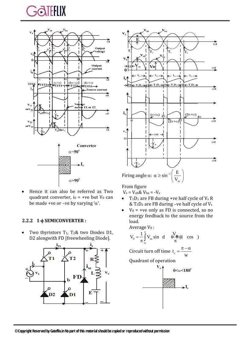
• Hence it can also be referred as Twoquadrant converter, i0 = +ve but V0 canbe made +ve or –ve by varying ‘α’.
2.2.2 1-φ SEMICONVERTER :
• Two thyristors T1, T2& two Diodes D1,D2 alongwith FD [freewheeling Diode].
vS
v0
0
i0
iS
vab vba
T1 T1 T2vab vba
α π
( + )π α 2π(2 + )π α3π
(3 + )π α
-Vm
ωt
ωt
ωt
ωt
ωt
ωt
T2
E
α Vm Vo
T D1 1T D2 2 T D1 1 T D2 2
iT1 iT2 iT1 iT2
4π
vT1
Oωtc
Firing angle α: 1
m
EsinV
− α ≥
From figure Vs = Vab& Vba = -Vs • T1D1 are FB during +ve half cycle of Vs R
& T2D2 are FB during –ve half cycle of Vs
• V0 = +ve only as FD is connected, so noenergy feedback to the source from theload.Average V0 :
m0 m
V1V V sin d (1 cos )π
α
= θ θ = + απ π∫
Circuit turn off time ct wπ−α
=
Quadrant of operation
© Copyright Reserved by Gateflix.in No part of this material should be copied or reproduced without permission
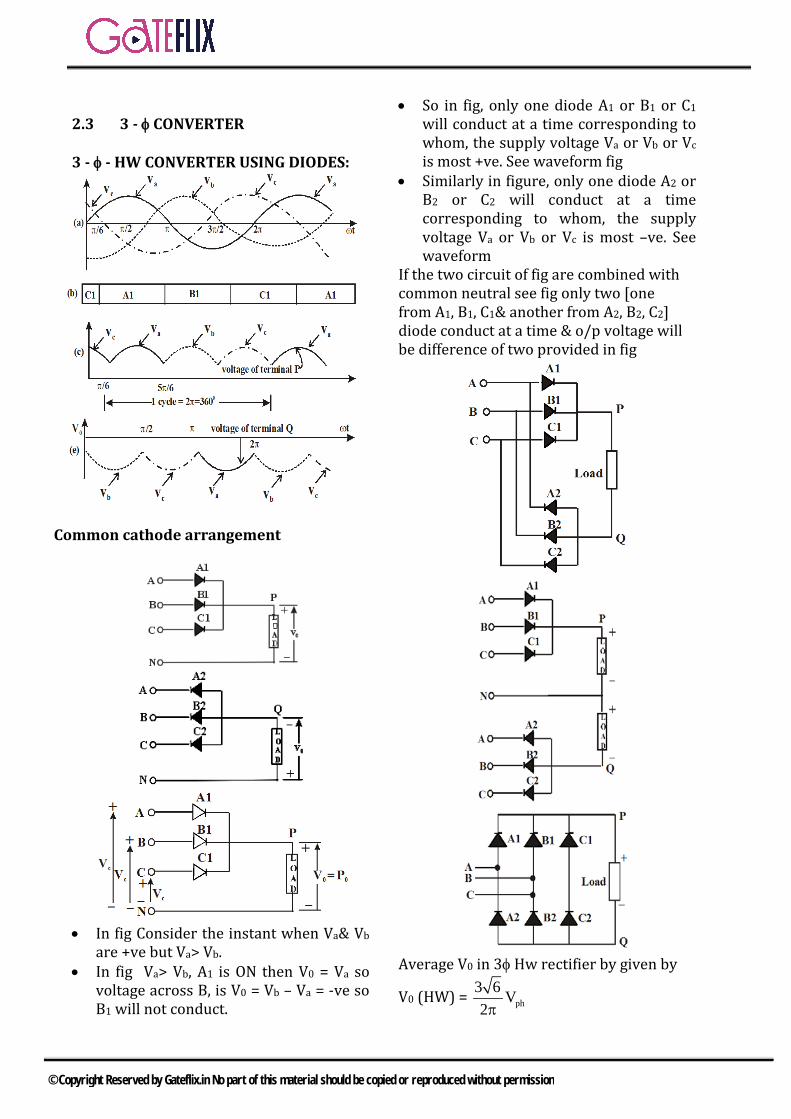
2.3 3 - φ CONVERTER
3 - φ - HW CONVERTER USING DIODES:
Common cathode arrangement
• In fig Consider the instant when Va& Vb
are +ve but Va> Vb.• In fig Va> Vb, A1 is ON then V0 = Va so
voltage across B, is V0 = Vb – Va = -ve soB1 will not conduct.
• So in fig, only one diode A1 or B1 or C1
will conduct at a time corresponding towhom, the supply voltage Va or Vb or Vc
is most +ve. See waveform fig• Similarly in figure, only one diode A2 or
B2 or C2 will conduct at a timecorresponding to whom, the supplyvoltage Va or Vb or Vc is most –ve. Seewaveform
If the two circuit of fig are combined with common neutral see fig only two [one from A1, B1, C1& another from A2, B2, C2] diode conduct at a time & o/p voltage will be difference of two provided in fig
Average V0 in 3φ Hw rectifier by given by
V0 (HW) = ph3 6 V2π
© Copyright Reserved by Gateflix.in No part of this material should be copied or reproduced without permission
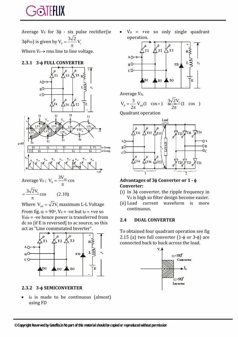
Average V0 for 3φ - six pulse rectifier(ie
3φFω) is given by 0 t3 2V V=π
Where Vt→ rms line to line voltage.
2.3.1 3-φ FULL CONVERTER
Average V0 ; ml0
3VV cos= απ
13 2V cos (2.10)= α − −π
Where ml 1V 2V= maximum L-L Voltage From fig. α = 90o, V0 = -ve but i0 = +ve so V0i0 = -ve hence power is transferred from dc so [if E is reversed] to ac source, so this act as “Line commutated Inverter”.
2.3.2 3-φ SEMICONVERTER
• i0 is made to be continuous (almost)using FD
• V0 = +ve so only single quadrantoperation.
Average V0,
10 ml
3 2V3V V (1 cos ) (1 cos )2 2
= + α = + απ π
Quadrant operation
Advantages of 3φ Converter or 1 - φ Converter: (i) In 3φ converter, the ripple frequency in
V0 is high so filter design become easier. (ii) Load current waveform is more
continuous.
2.4 DUAL CONVERTER
To obtained four quadrant operation see fig 2.15 (a) two full converter (1-φ or 3-φ) are connected back to back across the load.
© Copyright Reserved by Gateflix.in No part of this material should be copied or reproduced without permission
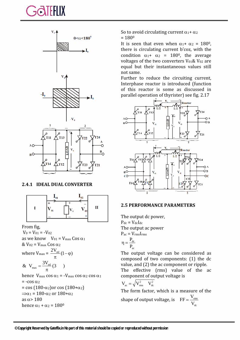
2.4.1 IDEAL DUAL CONVERTER
From fig, V0 = V01 = -V02 as we know V01 = Vmax Cos α1 & V02 = Vmax Cos α2
where Vmax = ml2V (1 )−ϕπ
mlmax
3V& V (3 )= −ϕπ
hence Vmax cos α1 = -Vmax cos α2 cos α1 = -cos α2 = cos (180-α2)or cos (180+α2) ⇒α1 = 180-α2 or 180+α2
as α> 180 hence α1 + α2 = 1800
So to avoid circulating current α1+ α2 = 1800 It is seen that even when α1+ α2 = 1800, there is circulating current b’coz, with the condition α1+ α2 = 1800, the average voltages of the two converters V01& V02 are equal but their instantaneous values still not same. Further to reduce the circuiting current, Interphase reactor is introduced (function of this reactor is some as discussed in parallel operation of thyrister) see fig. 2.17
2.5 PERFORMANCE PARAMETERS
The output dc power, Pdc = VdcIdc The output ac power Pac = VrmsIrms
dc
ac
PP
η =
The output voltage can be considered as composed of two components: (1) the dc value, and (2) the ac component or ripple. The effective (rms) value of the ac component of output voltage is
2 2ac rms dcV V V= −
The form factor, which is a measure of the
shape of output voltage, is rms
dc
VFFV
=
© Copyright Reserved by Gateflix.in No part of this material should be copied or reproduced without permission
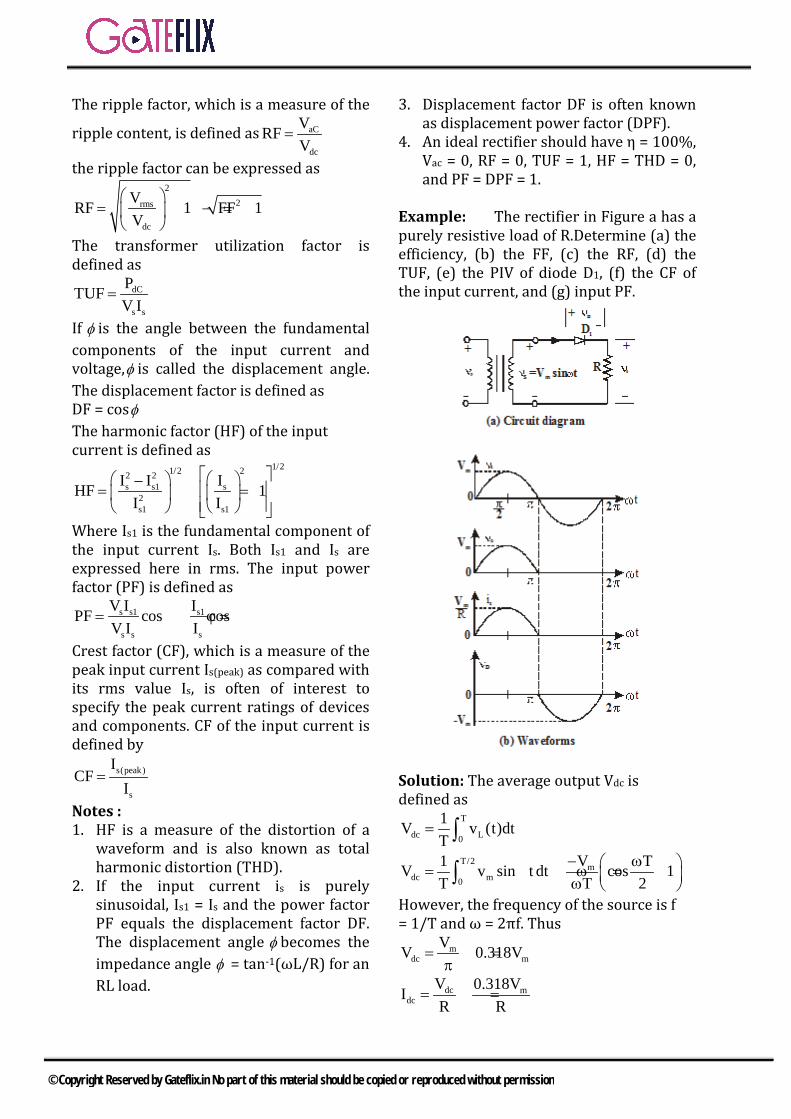
The ripple factor, which is a measure of the
ripple content, is defined as aC
dc
VRFV
=
the ripple factor can be expressed as 2
2rms
dc
VRF 1 FF 1V
= − = −
The transformer utilization factor is defined as
dC
s s
PTUFV I
=
If φ is the angle between the fundamental components of the input current and voltage,φ is called the displacement angle. The displacement factor is defined as DF = cosφ The harmonic factor (HF) of the input current is defined as
1/21/2 22 2s s1 s
2s1 s1
I I IHF 1I I
− = = −
Where Is1 is the fundamental component of the input current Is. Both Is1 and Is are expressed here in rms. The input power factor (PF) is defined as
s s1 s1
s s s
V I IPF cos cosV I I
= ϕ = ϕ
Crest factor (CF), which is a measure of the peak input current Is(peak) as compared with its rms value Is, is often of interest to specify the peak current ratings of devices and components. CF of the input current is defined by
s(peak)
s
ICF
I=
Notes : 1. HF is a measure of the distortion of a
waveform and is also known as totalharmonic distortion (THD).
2. If the input current is is purelysinusoidal, Is1 = Is and the power factorPF equals the displacement factor DF.The displacement angle φ becomes theimpedance angle φ = tan-1(ωL/R) for anRL load.
3. Displacement factor DF is often knownas displacement power factor (DPF).
4. An ideal rectifier should have η = 100%,Vac = 0, RF = 0, TUF = 1, HF = THD = 0,and PF = DPF = 1.
Example: The rectifier in Figure a has a purely resistive load of R.Determine (a) the efficiency, (b) the FF, (c) the RF, (d) the TUF, (e) the PIV of diode D1, (f) the CF of the input current, and (g) input PF.
Solution: The average output Vdc is defined as
T
dc L0
1V v (t)dtT
= ∫T/2 m
dc m0
V1 TV v sin t dt cos 1T T 2
− ω = ω = − ω ∫
However, the frequency of the source is f = 1/T and ω = 2πf. Thus
mdc m
VV 0.318V= =πdc m
dcV 0.318VIR R
= =
© Copyright Reserved by Gateflix.in No part of this material should be copied or reproduced without permission
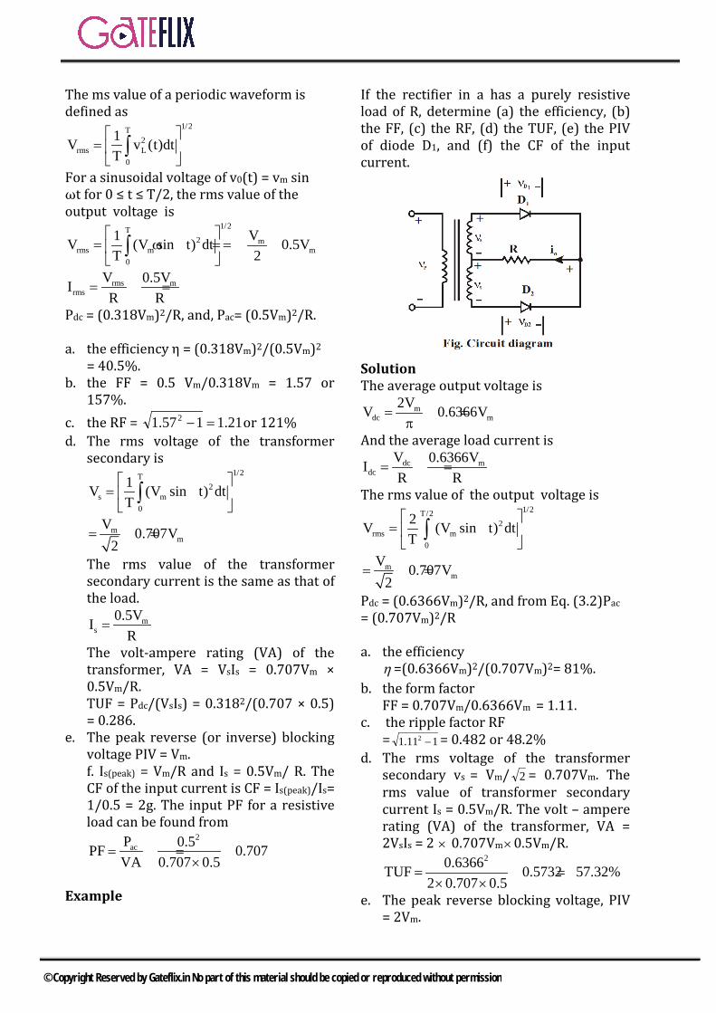
The ms value of a periodic waveform is defined as
1/2T2
rms L0
1V v (t)dtT
= ∫
For a sinusoidal voltage of v0(t) = vm sin ωt for 0 ≤ t ≤ T/2, the rms value of the output voltage is
1/2T2 m
rms m m0
V1V (V sin t) dt 0.5VT 2
= ω = = ∫
rms mrms
V 0.5VIR R
= =
Pdc = (0.318Vm)2/R, and, Pac= (0.5Vm)2/R.
a. the efficiency η = (0.318Vm)2/(0.5Vm)2
= 40.5%.b. the FF = 0.5 Vm/0.318Vm = 1.57 or
157%. c. the RF = 21.1157.1 2 =− or 121%d. The rms voltage of the transformer
secondary is1/2T
2s m
0
1V (V sin t) dtT
= ω ∫
mm
V 0.707V2
= =
The rms value of the transformer secondary current is the same as that of the load.
ms
0.5VIR
=
The volt-ampere rating (VA) of the transformer, VA = VsIs = 0.707Vm × 0.5Vm/R. TUF = Pdc/(VsIs) = 0.3182/(0.707 × 0.5) = 0.286.
e. The peak reverse (or inverse) blockingvoltage PIV = Vm.f. Is(peak) = Vm/R and Is = 0.5Vm/ R. TheCF of the input current is CF = Is(peak)/Is= 1/0.5 = 2g. The input PF for a resistive load can be found from
2acP 0.5PF 0.707
VA 0.707 0.5= = =
×
Example
If the rectifier in a has a purely resistive load of R, determine (a) the efficiency, (b) the FF, (c) the RF, (d) the TUF, (e) the PIV of diode D1, and (f) the CF of the input current.
Solution The average output voltage is
mdc m
2VV 0.6366V= =π
And the average load current is dc m
dcV 0.6366VIR R
= =
The rms value of the output voltage is 1/2T/2
2rms m
0
2V (V sin t) dtT
= ω ∫
mm
V 0.707V2
= =
Pdc = (0.6366Vm)2/R, and from Eq. (3.2)Pac
= (0.707Vm)2/R
a. the efficiencyη =(0.6366Vm)2/(0.707Vm)2= 81%.
b. the form factorFF = 0.707Vm/0.6366Vm = 1.11.
c. the ripple factor RF= 111.1 2 − = 0.482 or 48.2%
d. The rms voltage of the transformersecondary vs = Vm/ 2 = 0.707Vm. Therms value of transformer secondarycurrent Is = 0.5Vm/R. The volt – ampererating (VA) of the transformer, VA =2VsIs = 2 × 0.707Vm×0.5Vm/R.
20.6366TUF 0.5732 57.32%2 0.707 0.5
= = =× ×
e. The peak reverse blocking voltage, PIV= 2Vm.
© Copyright Reserved by Gateflix.in No part of this material should be copied or reproduced without permission
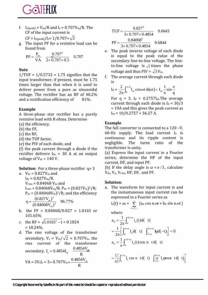
f. Is(peak) = Vm/R and Is = 0.707Vm/R. TheCF of the input current isCF = Is(peak)/Is= 1/0.707= 2
g. The input PF for a resistive load can befound from
2acP 0.707PF 0.707
VA 2 0.707 0.5= = =
× ×
Note 1/TUF = 1/0.5732 = 1.75 signifies that the input transformer, if present, must be 1.75 times larger than that when it is used to deliver power from a pure ac sinusoidal voltage. The rectifier has an RF of 48.2% and a rectification efficiency of 81%.
Example A three-phase star rectifier has a purely resistive load with R ohms. Determine (a) the efficiency, (b) the FF, (c) the RF, (d) the TUF factor, (e) the PIV of each diode, and (f) the peak current through a diode if the rectifier delivers Idc = 30 A at an output voltage of Vdc = 140 V.
Solution: For a three-phase rectifier q= 3 a. Vdc = 0.827Vm and
Idc = 0.827Vm/R.Vrms = 0.84068 Vm andIrms = 0.84068Vm/R. Pdc = (0.827Vm)2/R;Pac = (0.84068Vm)2/R; and the efficiency
2m
2m
(0.827V ) 96.77%(0.84068V )
η = =
b. the FF = 0.84068/0.827 = 1.0165 or101.65%
c. the RF = 21.0165 1− = 0.1824= 18.24%.
d. The rms voltage of the transformersecondary, Vs = Vm/ 2 = 0.707Vm. therms current of the transformer
secondary, ms m
0.4854VI 0.4854IR
= =
VA = 3VsIs = 3×0.707Vm m0.4854VR
×
20.827TUF 0.66433 0.707 0.4854
= =× ×
20.84068PF 0.68443 0.707 0.4854
= =× ×
e. The peak inverse voltage of each diodeis equal to the peak value of thesecondary line-to-line voltage. The line-to-line voltage is 3 times the phasevoltage and thus PIV = 3 Vm.
f. The average current through each diodeis
Id =/q
m m0
2 1I cos t d( t) I sin2 q
π πω ω =
π π∫For q = 3, Id = 0.2757Im.The average current through each diode is Id = 30/3 = 10A and this gives the peak current as Im = 10/0.2757 = 36.27 A.
Example The full converter is connected to a 120 –V, 60-Hz supply. The load current Ia is continuous and its ripple content is negligible. The turns ratio of the transformer is unity. (a) Express the input current in a Fourier series; determine the HF of the input current, DF, and input PF. (b) If the delay angle is α = 3/π , calculate Vdc, Vn, Vrms, HF, DF, and PF.
Solution: a. The waveform for input current is and
the instantaneous input current can beexpressed in a Fourier series asis(t) = a0 + ∑
∞
= ,....2,1n
(an cos n tω + bn sin n tω )
where 2
0 s1a i (t)d( t)
2π+α
α= ω
π ∫2
a a1 I d( t) I d( t)
2π+α π+α
α π+α
= ω − ω π ∫ ∫ 0=
2
n s1a i (t) cos n t d( t)
π+α
α= ω ωπ ∫
2
a a1 I cos n t d( t) I cos n t d( t)
π+α π+α
α π+α
= ω ω − ω ω π ∫ ∫
© Copyright Reserved by Gateflix.in No part of this material should be copied or reproduced without permission
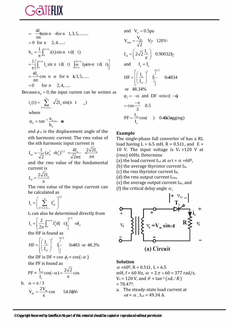
a4I sin n for n 1,3,5,........n
=− α =π
0 for n 2,4......= =
n1b i(t)sin n t d( t)
π+α
α= ω ωπ ∫
2
a a1 I sin n t d( t) I sin n t d( t)
π+α π+α
α π+α
= ω ω − ω ω π ∫ ∫a4I cos n for n 1,3,5,.....
n= α =
π0 for n 2,4,.....= =
0Becausea 0, the input current can be written as=
s n nn 1,3,5,...
i (t) 2I sin(n t )∞
=
= ω +ϕ∑where
1 nn
n
atan nb
−ϕ = = − α
and φ n is the displacement angle of the nth harmonic current. The rms value of the nth harmonic input current is
2 2 1/2 a asn n n
4I 2 2I1I (a b )n2 2n
= + = =ππ
and the rms value of the fundamental current is
as1
2 2II =π
The rms value of the input current can be calculated as
1/22
s snn 1,3,5,....
I I∞
=
= ∑
Is can also be determined directly from 1/2
2s a a
2I I d( t) I2
π+α
α
= ω = π ∫the HF is found as
1/22
s
s1
IHF 1 0.483 or 48.3%I
= − =
the DF is DF = cos 1φ = cos(-α ) the PF is found as PF = s1
s
I 2 2cos( ) cosI
−α = απ
b. / 3α = πm
dc2VV cos 54.02V= α =π
nand V 0.5pu=
mrms s
VV V 120V2
= = =
a
s1 aII 2 2 0.90032I = = π
s aand I I=
1/22
s
s1
IHF 1 0.4834I
= − =
or 48.34%
1 and DF cos t( )ϕ = −α = −α
cos 0.53−π
= =
s1
s
IPF cos( ) 0.45(lagging)I
= −α =
Example The single-phase full converter of has a RL load having L = 6.5 mH, R = 0.5Ω , and E = 10 V. The input voltage is Vs =120 V at (rms) 60Hz. Determine (a) the load current ILo at ω t = α =600, (b) the average thyristor current IA, (c) the rms thyristor current IR, (d) the rms output current Irms,
(e) the average output current Idc, and (f) the critical delay angle cα
Solution α =600, R = 0.5Ω , L = 6.5 mH, f = 60 Hz, ω = 2π ×60 = 377 rad/s, Vs = 120 V, and θ = tan-1 ( RL /ω ) = 78.470. a. The steady-state load current at
tω = α , ILo = 49.34 A.
© Copyright Reserved by Gateflix.in No part of this material should be copied or reproduced without permission
b. The numerical integration of iL in yieldsthe average thyristor current as IA =44.05A.
c. By numerical integration of i 2L between
the limits tω = α to π +α , we get therms thyristor current as IR = 63.71 A.
d. The rms output current Irms = 2 IR = 2×63.71 = 90.1A
e. The average output current Idc = 2IA = 2×44.04 = 88.1 A.by iteration we find the critical delayangle cα = 73.230.
© Copyright Reserved by Gateflix.in No part of this material should be copied or reproduced without permission
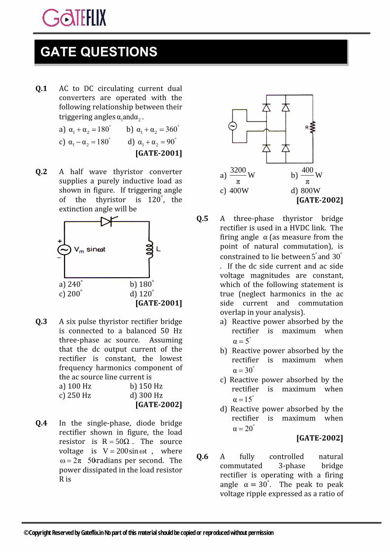
Q.1 AC to DC circulating current dual converters are operated with the following relationship between their triggering angles 1 2α andα . a) °
1 2α α 180+ = b) °1 2α α 360+ =
c) °1 2α α 180− = d) °
1 2α α 90+ = [GATE-2001]
Q.2 A half wave thyristor converter supplies a purely inductive load as shown in figure. If triggering angle of the thyristor is 120°, the extinction angle will be
a) 240° b) 180°
c) 200° d) 120°
[GATE-2001]
Q.3 A six pulse thyristor rectifier bridge is connected to a balanced 50 Hz three-phase ac source. Assuming that the dc output current of the rectifier is constant, the lowest frequency harmonics component of the ac source line current is a) 100 Hz b) 150 Hzc) 250 Hz d) 300 Hz
[GATE-2002]
Q.4 In the single-phase, diode bridge rectifier shown in figure, the load resistor is R 50Ω= . The source voltage is V 200sin ωt= , where ω 2π 50= × radians per second. The power dissipated in the load resistor R is
a) 3200 Wπ
b) 400 Wπ
c) 400W d) 800W [GATE-2002]
Q.5 A three-phase thyristor bridge rectifier is used in a HVDC link. The firing angle α (as measure from the point of natural commutation), is constrained to lie between °5 and °30. If the dc side current and ac side voltage magnitudes are constant, which of the following statement is true (neglect harmonics in the ac side current and commutation overlap in your analysis). a) Reactive power absorbed by the
rectifier is maximum when°α 5=
b) Reactive power absorbed by therectifier is maximum when
°α 30=c) Reactive power absorbed by the
rectifier is maximum when°α 15=
d) Reactive power absorbed by therectifier is maximum when
°α 20= [GATE-2002]
Q.6 A fully controlled natural commutated 3-phase bridge rectifier is operating with a firing angle α = 30°. The peak to peak voltage ripple expressed as a ratio of
GATE QUESTIONS
© Copyright Reserved by Gateflix.in No part of this material should be copied or reproduced without permission
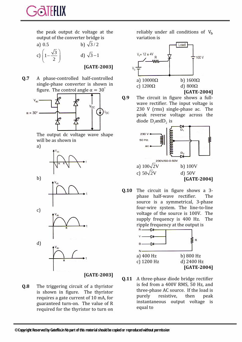
the peak output dc voltage at the output of the converter bridge is a) 0.5 b) 3 / 2
c) 312
−
d) 3 1−
[GATE-2003]
Q.7 A phase-controlled half-controlled single-phase converter is shown in figure. The control angle α = 30°
The output dc voltage wave shape will be as shown in a)
b)
c)
d)
[GATE-2003]
Q.8 The triggering circuit of a thyristor is shown in figure. The thyristor requires a gate current of 10 mA, for guaranteed turn-on. The value of R required for the thyristor to turn on
reliably under all conditions of Vb variation is
a) 10000Ω b) 1600Ωc) 1200Ω d) 800Ω
[GATE-2004] Q.9 The circuit in figure shows a full-
wave rectifier. The input voltage is 230 V (rms) single-phase ac. The peak reverse voltage across the diode 1 2D andD is
a) 100 2V b) 100Vc) 50 2V d) 50V
[GATE-2004]
Q.10 The circuit in figure shows a 3-phase half-wave rectifier. The source is a symmetrical, 3-phase four-wire system. The line-to-line voltage of the source is 100V. The supply frequency is 400 Hz. The ripple frequency at the output is
a) 400 Hz b) 800 Hzc) 1200 Hz d) 2400 Hz
[GATE-2004]
Q.11 A three-phase diode bridge rectifier is fed from a 400V RMS, 50 Hz, and three-phase AC source. If the load is purely resistive, then peak instantaneous output voltage is equal to
© Copyright Reserved by Gateflix.in No part of this material should be copied or reproduced without permission
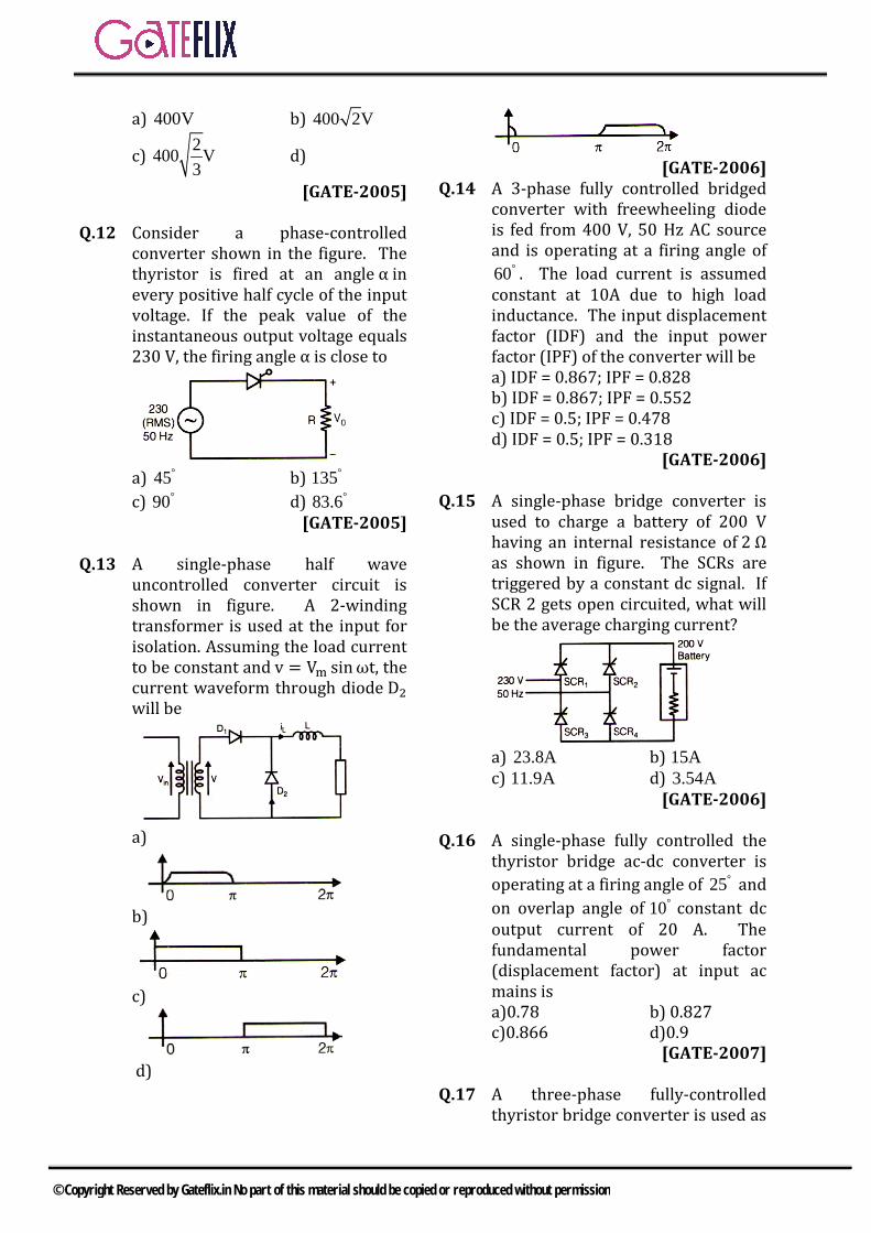
a) 400V b) 400 2V
c) 2400 V3
d)
[GATE-2005]
Q.12 Consider a phase-controlled converter shown in the figure. The thyristor is fired at an angle α in every positive half cycle of the input voltage. If the peak value of the instantaneous output voltage equals 230 V, the firing angle α is close to
a) °45 b) °135c) °90 d) °83.6
[GATE-2005]
Q.13 A single-phase half wave uncontrolled converter circuit is shown in figure. A 2-winding transformer is used at the input for isolation. Assuming the load current to be constant and v = Vm sinωt, the current waveform through diode D2 will be
a)
b)
c)
d)
[GATE-2006] Q.14 A 3-phase fully controlled bridged
converter with freewheeling diode is fed from 400 V, 50 Hz AC source and is operating at a firing angle of
°60 . The load current is assumed constant at 10A due to high load inductance. The input displacement factor (IDF) and the input power factor (IPF) of the converter will be a) IDF = 0.867; IPF = 0.828b) IDF = 0.867; IPF = 0.552c) IDF = 0.5; IPF = 0.478d) IDF = 0.5; IPF = 0.318
[GATE-2006]
Q.15 A single-phase bridge converter is used to charge a battery of 200 V having an internal resistance of 2 Ω as shown in figure. The SCRs are triggered by a constant dc signal. If SCR 2 gets open circuited, what will be the average charging current?
a) 23.8A b) 15Ac) 11.9A d) 3.54A
[GATE-2006]
Q.16 A single-phase fully controlled the thyristor bridge ac-dc converter is operating at a firing angle of °25 and on overlap angle of °10 constant dc output current of 20 A. The fundamental power factor (displacement factor) at input ac mains is a)0.78 b) 0.827c)0.866 d)0.9
[GATE-2007]
Q.17 A three-phase fully-controlled thyristor bridge converter is used as
© Copyright Reserved by Gateflix.in No part of this material should be copied or reproduced without permission
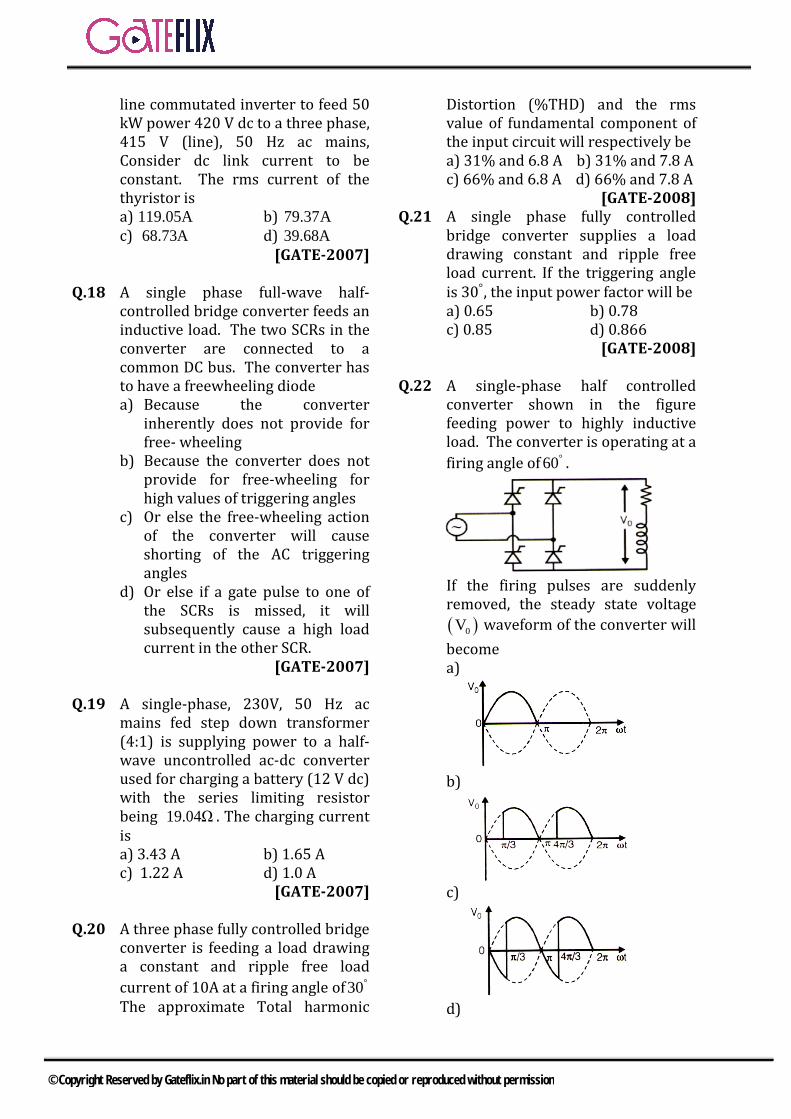
line commutated inverter to feed 50 kW power 420 V dc to a three phase, 415 V (line), 50 Hz ac mains, Consider dc link current to be constant. The rms current of the thyristor is a) 119.05A b) 79.37Ac) 68.73A d) 39.68A
[GATE-2007]
Q.18 A single phase full-wave half-controlled bridge converter feeds an inductive load. The two SCRs in the converter are connected to a common DC bus. The converter has to have a freewheeling diode a) Because the converter
inherently does not provide for free- wheeling
b) Because the converter does notprovide for free-wheeling forhigh values of triggering angles
c) Or else the free-wheeling actionof the converter will causeshorting of the AC triggeringangles
d) Or else if a gate pulse to one ofthe SCRs is missed, it willsubsequently cause a high loadcurrent in the other SCR.
[GATE-2007]
Q.19 A single-phase, 230V, 50 Hz ac mains fed step down transformer (4:1) is supplying power to a half-wave uncontrolled ac-dc converter used for charging a battery (12 V dc) with the series limiting resistor being 19.04Ω . The charging current is a) 3.43 A b) 1.65 Ac) 1.22 A d) 1.0 A
[GATE-2007]
Q.20 A three phase fully controlled bridge converter is feeding a load drawing a constant and ripple free load current of 10A at a firing angle of °30The approximate Total harmonic
Distortion (%THD) and the rms value of fundamental component of the input circuit will respectively be a) 31% and 6.8 A b) 31% and 7.8 Ac) 66% and 6.8 A d) 66% and 7.8 A
[GATE-2008] Q.21 A single phase fully controlled
bridge converter supplies a load drawing constant and ripple free load current. If the triggering angle is 30°, the input power factor will be a) 0.65 b) 0.78c) 0.85 d) 0.866
[GATE-2008]
Q.22 A single-phase half controlled converter shown in the figure feeding power to highly inductive load. The converter is operating at a firing angle of °60 .
If the firing pulses are suddenly removed, the steady state voltage ( )0V waveform of the converter will become a)
b)
c)
d)
© Copyright Reserved by Gateflix.in No part of this material should be copied or reproduced without permission
[GATE-2008] Q.23 The fully controlled thyristor
converter in the figure is fed from a single-phase source. When the firing angle is 0° , the dc output voltage of the converter is 300V. What will be the output voltage for a firing angle of 60° , assuming continuous conduction?
a) 150 V b) 210 Vc) 300 V d) 100πV
[GATE-2010]
Q.24 A half-controlled single-phase bridge rectifier is supplying an R-L load. It is operated at a firing angle α and the load current is continuous. The fraction of cycle that the freewheeling diode conduct is
a) 12
b) α1π
−
c) α
2πd)
απ
[GATE-2012]
Q.25 Thyristor T in the figure below is initially off and is triggered with a single pulse of width 10 µs. It is
given that 100L μH andπ
=
100C μFπ
=
. Assuming latching
and holding currents of the thyristor are both zero and the initial charge on C is zero, T conducts for
a) 10μs b) 50μsc) 100μs d) 200μs
[GATE-2013]
Q.26 The figure shows the circuit of a rectifier fed from a 230 V (rms), 50 Hz sinusoidal voltage source. If we want to replace the current source with a resistor so that the rms value of the current supplied by the voltage source remains unchanged, the value of the resistance (in ohms) is _____.(Assume diodes to be ideal.)
[GATE-2014]
Q.27 The figure shows the circuit diagram of a rectifier. The load consists of a resistance 10 Ω and an inductance 0.05 H connected in series. Assuming ideal thyristor and ideal diode, the thyristor firing angle (in degree) needed to obtain an average load voltage of 70 V is ____.
[GATE-2014]
© Copyright Reserved by Gateflix.in No part of this material should be copied or reproduced without permission
Q.28 A fully controlled converter bridge feeds a highly inductive load with ripple free load current. The input supply (vs ) to the bridge is a sinusoidal source. Triggering angle of the bridge converter is o 30α = . The input power factor of the bridge is
[GATE-2014]
Q.29 A three-phase fully controlled bridge converter is fed through star-delta transformer as shown in the figure.
The converter is operated at a firing angle of o30 Assuming the load current (I0) to be virtually constant at 1 p.u. and transformer to be an ideal one, the input phase current waveform is
[GATE-2014]
Q.30 A diode circuit feeds an ideal inductor as shown in the figure. Given
( )100sin V, where =100 rad/ss tν = ω ω πand L = 31.83 mH. The initial value of inductor current is zero. Switch S is closed at t = 2.5ms. The peak value of inductor current iL (in A) in the first cycle is _____.
[GATE-2014]
Q.31 In the following circuit, the input voltage Vin is 100 sin (100πt)V. For 100πR C = 50, the average voltages across R (in volts) under steady-state is nearest to
© Copyright Reserved by Gateflix.in No part of this material should be copied or reproduced without permission
(a)100 (b)31.8 (c)200 (d)63.6
[GATE-2015]
Q.32 In the given rectifier, the delay angle of the thyristor T1 measured from the positive going zero crossing of Vs is 30 ° . If the input voltage Vs is 100 sin (100πt)V , the average voltage across R (in Volt) under steady-state is ______.
[GATE-2015]
Q.33 A single-phase thyristor-bridge rectifier is fed from a 230 V, 50 Hz, single-phase AC mains. If it is delivering a constant DC current of 10 A, at firing angle of o30 , then value of the power factor at AC mains is (A) 0.87 (B) 0.9 (C) 0.78 (D) 0.45
[GATE-2016]
Q.34 A three - phase diode bridge rectifier is feeding a constant DC current of 100A to a highly inductive load. If three - phase, 415V,50Hz AC source is supplying to this bridge rectifier then the rms value of the current in each diode, in ampere, is ________.
[GATE-2016]
Q.35 A full - bridge converter supplying an RLE load is shown in figure. The firing angle of the bridge converter is 120°. The supply voltage
Vm(t) = 200πSin(100πt) V, R = 20Ω, E = 800V. The inductor L is large enough to make the output current IL a smooth dc current. Switches are lossless. The real power feedback to the source, in kW, is __________.
[GATE-2016]
Q.36 A single - phase bi - directional voltage source converter (VSC) is shown in the figure below. All devices are ideal. It is used to charge a battery at 400V with power of 5kW from a source Vs = 220 V(rms), 50HZ sinusoidal AC mains at unity p.f. If its AC side interfacing inductor is 5mH and the switches are operated at 20KHz, then the phase shift (δ) between AC mains voltage (Vs) and fundamental AC rms VSC voltage (Vc1), in degree, is ________.
[GATE-2016]
© Copyright Reserved by Gateflix.in No part of this material should be copied or reproduced without permission
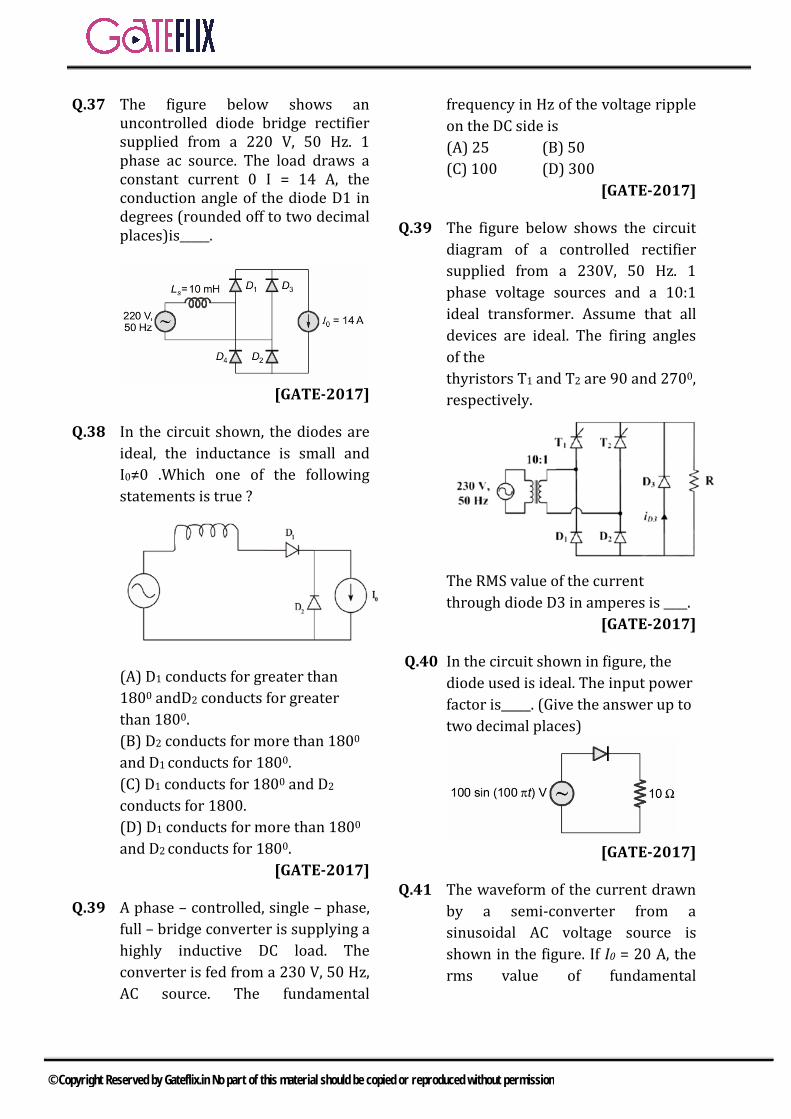
Q.37 The figure below shows an uncontrolled diode bridge rectifier supplied from a 220 V, 50 Hz. 1 phase ac source. The load draws a constant current 0 Ι = 14 A, the conduction angle of the diode D1 in degrees (rounded off to two decimal places)is_____.
[GATE-2017]
Q.38 In the circuit shown, the diodes are ideal, the inductance is small and Ι0≠0 .Which one of the following statements is true ?
(A) D1 conducts for greater than 1800 andD2 conducts for greater than 1800. (B) D2 conducts for more than 1800 and D1 conducts for 1800. (C) D1 conducts for 1800 and D2 conducts for 1800. (D) D1 conducts for more than 1800 and D2 conducts for 1800.
[GATE-2017]
Q.39 A phase – controlled, single – phase, full – bridge converter is supplying a highly inductive DC load. The converter is fed from a 230 V, 50 Hz, AC source. The fundamental
frequency in Hz of the voltage ripple on the DC side is (A) 25 (B) 50 (C) 100 (D) 300
[GATE-2017]
Q.39 The figure below shows the circuit diagram of a controlled rectifier supplied from a 230V, 50 Hz. 1 phase voltage sources and a 10:1 ideal transformer. Assume that all devices are ideal. The firing angles of the thyristors T1 and T2 are 90 and 2700, respectively.
The RMS value of the current through diode D3 in amperes is ____.
[GATE-2017]
Q.40 In the circuit shown in figure, the diode used is ideal. The input power factor is_____. (Give the answer up to two decimal places)
[GATE-2017]
Q.41 The waveform of the current drawn by a semi-converter from a sinusoidal AC voltage source is shown in the figure. If I0 = 20 A, the rms value of fundamental
© Copyright Reserved by Gateflix.in No part of this material should be copied or reproduced without permission
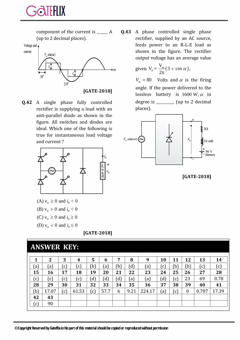
component of the current is ______ A (up to 2 decimal places).
[GATE-2018]
Q.42 A single phase fully controlled rectifier is supplying a load with an anti-parallel diode as shown in the figure. All switches and diodes are ideal. Which one of the following is true for instantaneous load voltage and current ?
0 0
0 0
0 0
0 0
(A) v 0 and < 0 (B) v 0 and < 0 (C) v 0 and 0 (D) v 0 and 0
iiii
≥
>
≥ ≥
< ≤
[GATE-2018]
Q.43 A phase controlled single phase rectifier, supplied by an AC source, feeds power to an R-L-E load as shown in the figure. The rectifier output voltage has an average value
given ( )m0
VV = 3 cos ,2
α+π
80mV = π Volts and α is the firing angle. If the power delivered to the lossless battery is 1600 W, α in degree is __________ (up to 2 decimal places).
[GATE-2018]
1 2 3 4 5 6 7 8 9 10 11 12 13 14 (a) (a) (c) (c) (b) (a) (b) (d) (a) (c) (b) (b) (c) (c) 15 16 17 18 19 20 21 22 23 24 25 26 27 28 (c) (c) (c) (c) (d) (d) (d) (a) (a) (d) (c) 23 69 0.78 28 29 30 31 32 33 34 35 36 37 38 39 40 41 (b) 17.07 (c) 61.53 (c) 57.7 6 9.21 224.17 (a) (c) 0 0.707 17.39 42 43 (c) 90
ANSWER KEY:
© Copyright Reserved by Gateflix.in No part of this material should be copied or reproduced without permission
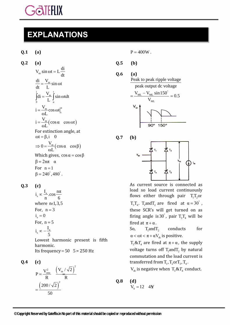
Q.1 (a)
Q.2 (a)
mdiV sin ωt Ldt
=
mVdi sin ωtdt L
=
i tm
0 α
Vdi sin ωtdtL
=∫ ∫αmt
Vi cos ωtωL
=
( )mVi cos α cos ωtωL
= −
For extinction angle, at ωt β,i 0= =
( )mV0 cos α cosβωL
⇒ = −
Which gives, cos α cosβ=β 2nπ α= ± For n 1=
° °β 240 ,480= .
Q.3 (c) a
sI nπi .cosn 6
∝
where n 1,3,5 For, n 3=
si 0= For, n 5=
as
Ii5
∝ −
Lowest harmonic present is fifth harmonic. Its frequency 50 5= × = 250 Hz
Q.4 (c)
( )22
mrmsV / 2VP
R R= =
( )2200 / 2
50=
P 400W= .
Q.5 (b)
Q.6 (a) Peak to peak ripple voltage
peak output dc voltage°
ML ML
ML
V V sin150V
−= 0.5=
Q.7 (b)
As current source is connected as load so load current continuously flows either through pair 1 2T T or
3 4T T . 1 2T andT are fired at °α 30= , these SCR’s will get turned on as firing angle is °30 , pair 3 4T T will be fired at π α+ . So, 1 2T andT conducts for
dcα ωt π αV< < + is positive.
3 4T &T are fired at π α+ , the supply voltage turns off 1 2T andT by natural commutation and the load current is transferred from 1 2 3 4T ,T orT ,T .
dcV is negative when 3 4T &T conduct.
Q.8 (d) bV 12 4V= ±
EXPLANATIONS
© Copyright Reserved by Gateflix.in No part of this material should be copied or reproduced without permission
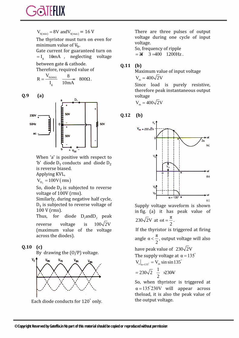
( ) ( )b min b maxV 8V andV= = 16 V The thyristor must turn on even for minimum value of Vb. Gate current for guaranteed turn on
gI 10mA= = , neglecting voltage between gate & cathode. Therefore, required value of
b(min)
g
V 8R 800ΩI 10mA
= = = .
Q.9 (a)
When ‘a’ is positive with respect to ‘b’ diode D1 conducts and diode D2 is reverse biased. Applying KVL,
( )2DV 100V rms=
So, diode D2 is subjected to reverse voltage of 100V (rms). Similarly, during negative half cycle, D1 is subjected to reverse voltage of 100 V (rms). Thus, for diode 1 2D andD peak
reverse voltage is 100 2V (maximum value of the voltage across the diodes).
Q.10 (c) By drawing the (O/P) voltage.
Each diode conducts for 120° only.
There are three pulses of output voltage during one cycle of input voltage. So, frequency of ripple
3f 3 400 1200Hz= = × = .
Q.11 (b) Maximum value of input voltage
mV 400 2V=Since load is purely resistive, therefore peak instantaneous output voltage
mV 400 2V=
Q.12 (b)
Supply voltage waveform is shown in fig. (a) it has peak value of
230 2V at πωt2
= .
If the thyristor is triggered at firing
angle πα2
< , output voltage will also
have peak value of 230 2V The supply voltage at °α 135=
°°
s mα 135V V sin sin135
==
1230 2 230V2
= × =
So, when thyristor is triggered at °α 135 230V= will appear across
theload, it is also the peak value of the output voltage.
© Copyright Reserved by Gateflix.in No part of this material should be copied or reproduced without permission
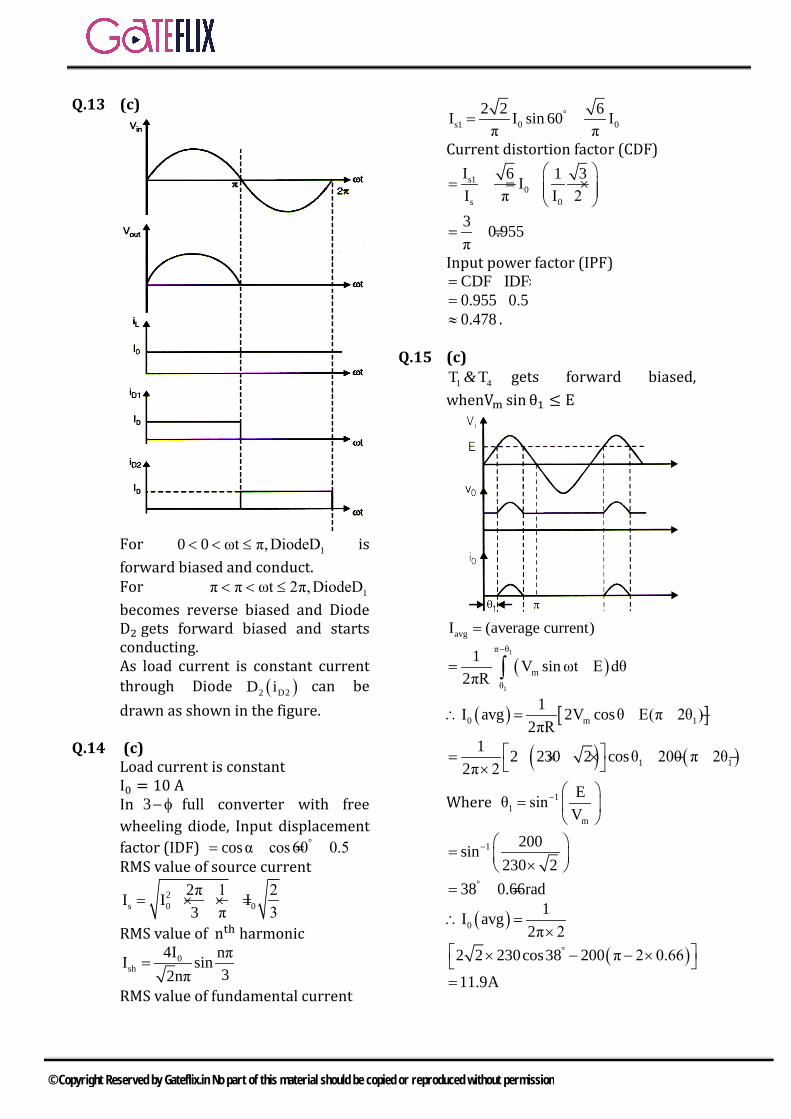
Q.13 (c)
For 10 0 ωt π,DiodeD< < ≤ is forward biased and conduct. For 1π π ωt 2π,DiodeD< < ≤becomes reverse biased and Diode D2 gets forward biased and starts conducting. As load current is constant current through Diode ( )2 D2D i can bedrawn as shown in the figure.
Q.14 (c) Load current is constant I0 = 10 A In 3− φ full converter with free wheeling diode, Input displacement factor (IDF) °cos α cos 60 0.5= = = RMS value of source current
2s 0 0
2π 1 2I I I3 π 3
= × × =
RMS value of nth harmonic 0
sh4I nπI sin
32nπ=
RMS value of fundamental current
°s1 0 0
2 2 6I I sin 60 Iπ π
= =
Current distortion factor (CDF)
s10
s 0
I 6 1 3II π I 2
= = ×
3 0.955π
= =
Input power factor (IPF) CDF IDF= × 0.955 0.5= × 0.478≈ .
Q.15 (c) 1 4T T& gets forward biased,
whenVm sinθ1 ≤ E
avgI (average current)=
( )1
1
π θ
mθ
1 V sin ωt E dθ2πR
−
= −∫
( ) [ ]0 m 11I avg 2V cosθ E(π 2θ )
2πR∴ = − −
( ) ( )1 11 2 230 2 cosθ 200 π 2θ
2π 2 = × × − − ×
Where 11
m
Eθ sinV
− =
1 200sin230 2
− = ×
°38 0.66rad= =
( )01I avg
2π 2∴ =
×( )°2 2 230cos38 200 π 2 0.66 × − − ×
11.9A=
© Copyright Reserved by Gateflix.in No part of this material should be copied or reproduced without permission
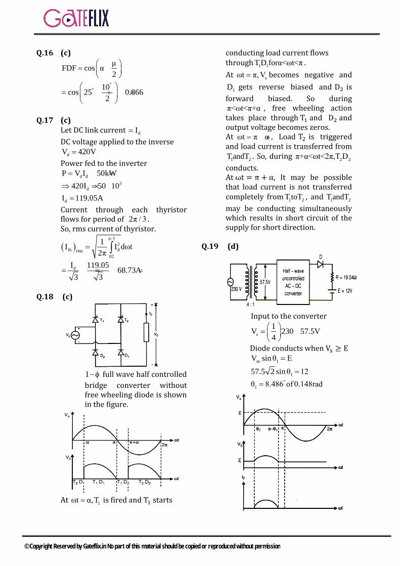
Q.16 (c) μFDF cos α2
= +
°° 10cos 25 0.866
2
= + =
Q.17 (c) Let DC link current dI=DC voltage applied to the inverse
dV 420V=Power fed to the inverter
d dP V I 50kW= =3
d420I 50 10⇒ = ×
dI 119.05A=Current through each thyristor flows for period of 2π / 3 . So, rms current of thyristor.
( )π/3
2th drms
02
1I I dωt2π
= ∫dI 119.05 68.73A3 3
= = =
Q.18 (c)
1− φ full wave half controlled bridge converter without free wheeling diode is shown in the figure.
At 1ωt α,T= is fired and T1 starts
conducting load current flows through 1 1T D forα<ωt<π . At sωt π,V= becomes negative and
1D gets reverse biased and D2 is forward biased. So during π<ωt<π+α , free wheeling action takes place through T1 and D2 and output voltage becomes zeros. At ωt π α= + , Load T2 is triggered and load current is transferred from
1 2T andT . So, during 2 2π+α<ωt<2π,T Dconducts. At ωt = π + α, It may be possible that load current is not transferred completely from 1 2T toT , and 1 2T andT may be conducting simultaneously which results in short circuit of the supply for short direction.
Q.19 (d)
Input to the converter
s1V 230 57.5V4
= −
Diode conducts when Vs ≥ E m 1V sin θ E=
157.5 2 sin θ 12=°
1θ 8.486 of 0.148rad=
© Copyright Reserved by Gateflix.in No part of this material should be copied or reproduced without permission
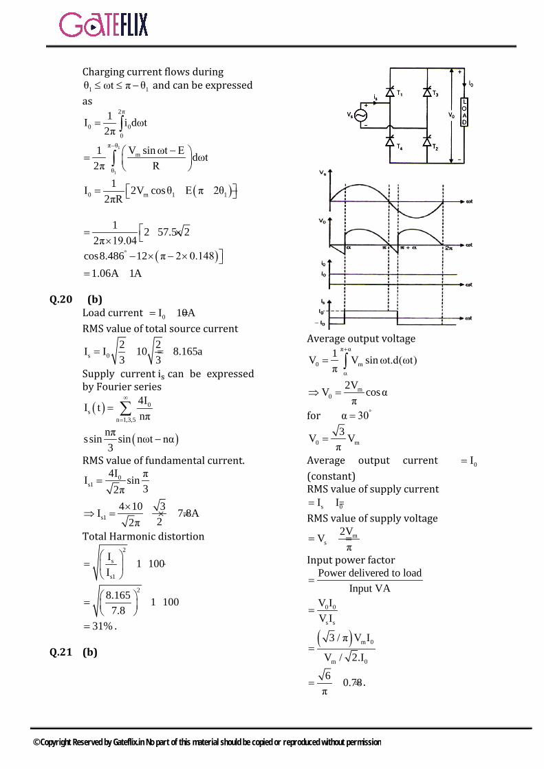
Charging current flows during 1 1θ ωt π θ≤ ≤ − and can be expressed
as 2π
00
01I i dωt
2π= ∫
1
1
π θm
θ
V sin ωt E1 dωt2π R
− − = ∫
( )0 m 1 11I 2V cosθ E π 2θ
2πR= − −
1 2 57.5 22π 19.04
= × ××( )°cos8.486 12 π 2 0.148 − × − ×
1.06A 1A= ≈
Q.20 (b) Load current 0I 10A= =RMS value of total source current
s 02 2I I 10 8.165a3 3
= = =
Supply current is can be expressed by Fourier series
( ) 0s
n 1,3,5
4II tnπ
∞
=
= ∑
( )nπssin sin nωt nα3
−
RMS value of fundamental current. 0
s14I πI sin
32π=
s14 10 3I 7.8A
22π×
⇒ = × =
Total Harmonic distortion 2
s
s1
I 1 100I
= − ×
28.165 1 1007.8
= − ×
31%= .
Q.21 (b)
Average output voltage π α
0 m1V V sin ωt.d(ωt)π
+
α
= ∫m
02VV cos α
π⇒ =
for °α 30=
0 m3V V
π=
Average output current 0I=(constant) RMS value of supply current
s 0I I= =RMS value of supply voltage
ms
2VVπ
= =
Input power factor Power delivered to load
Input VA=
0 0
s s
V IV I
=
( ) m 0
m 0
3 / π V I
V / 2.I=
6 0.78π
= = .
© Copyright Reserved by Gateflix.in No part of this material should be copied or reproduced without permission
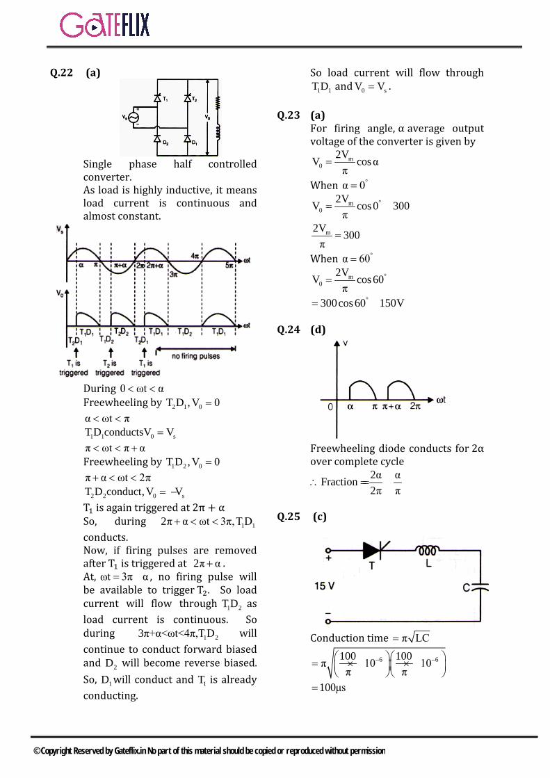
Q.22 (a)
Single phase half controlled converter. As load is highly inductive, it means load current is continuous and almost constant.
During 0 ωt α< < Freewheeling by 2 1 0T D ,V 0= α ωt π< <
1 1 0 sT D conductsV V=π ωt π α< < + Freewheeling by 1 2 0T D ,V 0= π α ωt 2π+ < <
2 2 0 sT D conduct,V V= −T1 is again triggered at 2π + α So, during 1 12π α ωt 3π,T D+ < <conducts. Now, if firing pulses are removed after T1 is triggered at 2π α+ . At, ωt 3π α= + , no firing pulse will be available to trigger T2. So load current will flow through 1 2T D as load current is continuous. So during 1 23π+α<ωt<4π,T D will continue to conduct forward biased and 2D will become reverse biased. So, 1D will conduct and 1T is already conducting.
So load current will flow through 1 1T D and 0 sV V= .
Q.23 (a) For firing angle, α average output voltage of the converter is given by
m0
2VV cos απ
=
When °α 0=°m
02VV cos 0 300
π= =
m2V 300π
=
When °α 60=°m
02VV cos 60
π=
°300cos 60 150V= =
Q.24 (d)
Freewheeling diode conducts for 2α over complete cycle
2α αFraction2π π
∴ = =
Q.25 (c)
Conduction time π LC=
6 6100 100π 10 10π π
− − = × ×
100μs=
© Copyright Reserved by Gateflix.in No part of this material should be copied or reproduced without permission
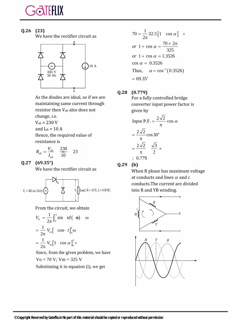
Q.26 (23) We have the rectifier circuit as
As the diodes are ideal, so if we are maintaining same current through resistor then Vab also does not change, i.e. Vab = 230 V and Iab = 10 A Hence, the required value of resistance is
230 2310
abab
ab
VRI
= = = Ω
Q.27 (69.35°) We have the rectifier circuit as
From the circuit, we obtain
( )
[ ]
[ ]
01 sin
21 cos
21 1 cos
2Since, from the given problem, we haveVo = 70 V; Vm = 325 VSubstituting it in equation (i), we get
Tm
Tm
V td t
V t
V
α
α
αα
π= ω ω
π
= − ωπ
= +π
∫
[ ]
( )1
o
170 32.5 1 cos2
70 21 cos325
1 cos 1.3526cos 0.3526Thus, cos 0.3526
69.35
or
or
α
α
αα
α −
= +π
× π+ =
+ ==
=
=
Q.28 (0.779) For a fully controlled bridge converter input power factor is given by
o
2 2Input P.F. cos
2 2 cos30
2 2 3
0.779
α=π
=π
= ×π 2
;Q.29 (b)
When R phase has maximum voltage at conducts and lines α and c conducts.The current are divided into R and YB winding.
© Copyright Reserved by Gateflix.in No part of this material should be copied or reproduced without permission
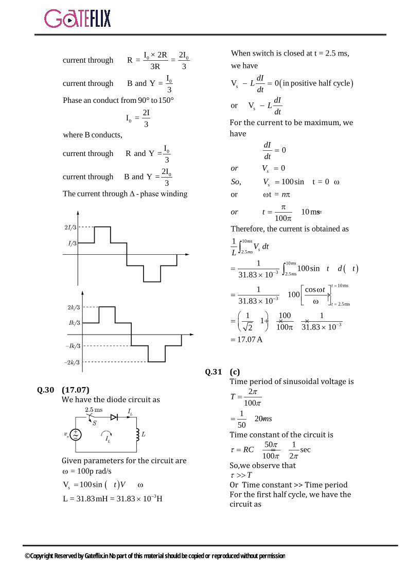
0 0
0
0
0
0
I × 2R 2Icurrent through R = =3R 3
Icurrent through B and Y =3
Phase an conduct from 90° to 150°2II =3
where B conducts,Icurrent through R and Y =3
2Icurrent through B and Y =3
The current through Δ - phase winding
Q.30 (17.07) We have the diode circuit as
Given parameters for the circuit are
( )s
3
V 100sin = 100p rad/s
L = 31.83mH = 31.83 10 H
t V−
ω
×
= ω
( )s
s
When switch is closed at t = 2.5 ms, we have
V 0 in positive half cycle
or V
dILdt
dILdt
− =
−
For the current to be maximum, we have
( )
10
2.5
10
3 2.5
10ms
32.5ms
0
0, 100sin t = 0
or t =
10ms100
Therefore, the current is obtained as1
1 100sin31.83 10
1 cos10031.83 10
1 100 11100 312
s
s
ms
sms
ms
ms
t
t
dIdt
or VSo V
n
or t
V dtL
t d t
t
−
=
−=
=
=
= ωω π
π= =
π
= ω + ω×
ω = × × ω
= + × × π
∫
∫
3.83 1017.07 A
−×=
Q.31 (c) Time period of sinusoidal voltage is
2100
1 2050
T
ms
ππ
=
= =
Time constant of the circuit is 50 1 sec
100 2RC πτ
π π= = =
So,we observe that Tτ >>
Or Time constant >> Time period For the first half cycle, we have the circuit as
© Copyright Reserved by Gateflix.in No part of this material should be copied or reproduced without permission
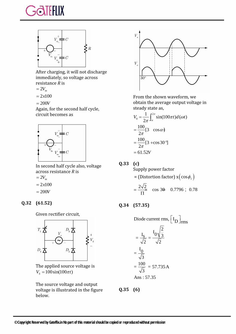
After charging, it will not discharge immediately, so voltage across resistance R is
22 100200
mVx
V
===
Again, for the second half cycle, circuit becomes as
In second half cycle also, voltage across resistance R is
22 100200
mVx
V
===
Q.32 (61.52)
Given rectifier circuit,
The applied source voltage is 100sin(100 )SV tπ=
The source voltage and output voltage is illustrated in the figure below.
From the shown waveform, we obtain the average output voltage in steady state as,
2
01 sin(100 ) ( )
2100 [3 cos ]2100 [3 cos30 ]261.52
V t d t
V
π
απ ω
π
απ
π
=
= +
= + °
=
∫
Q.33 (c) Supply power factor = (Distortion factor) x ( )1cosφ
2 2 cos 30 0.7796 0.78= × =Π
;
Q.34 (57.35)
Diode current rms, ID rms2I0I 3s= =
2 2I0=
3100= = 57.735A
3Ans : 57.35
Q.35 (6)
© Copyright Reserved by Gateflix.in No part of this material should be copied or reproduced without permission
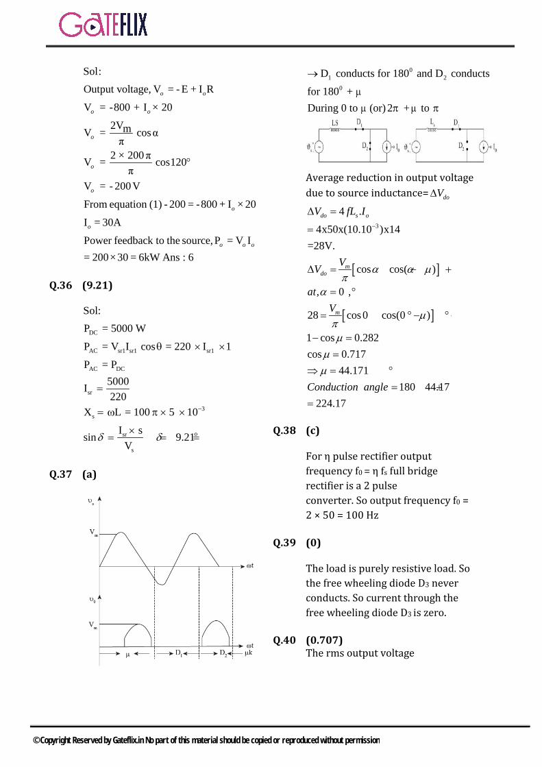
Sol:Output voltage, V = - E + I RV = -800 + I × 20
2VmV = cos απ
2 × 200 πV = cos120π
V = - 200VFrom equation (1) - 200 = -800 + I × 20I = 30APower feedback to the source,P = V I= 200 × 30 = 6kW Ans : 6
o o
o o
o
o
o
o
o
o o o
°
Q.36 (9.21)
DC
AC sr1 sr1 sr1
AC DC
sr
3s
osr
s
Sol:P = 5000 WP = V I cos = 220 I 1P = P
5000I220
X L = 100 5 10I ssin 9.21
Vδ δ
−
θ × ×
=
= ω π × ×
×= = =
Q.37 (a)
01 2
0
D conducts for 180 and D conductsfor 180 + During 0 to (or) 2 + to
→
π π
Average reduction in output voltage due to source inductance= doV∆
[ ]
[ ]
3
4 .4x50x(10.10 )x14
=28V.
cos cos( )
, 0 ,
28 cos 0 cos(0 )
1 cos 0.282cos 0.717
44.171180 44.17
224.17
do s o
mdo
m
V fL I
VV
atV
Conduction angle
α α µπ
α
µπµ
µµ
−
∆ =
=
∆ = − +
= °
= ° − ° +
− ==
⇒ = °= +
=
Q.38 (c)
For η pulse rectifier output frequency f0 = η fs full bridge rectifier is a 2 pulse converter. So output frequency f0 = 2 × 50 = 100 Hz
Q.39 (0)
The load is purely resistive load. So the free wheeling diode D3 never conducts. So current through the free wheeling diode D3 is zero.
Q.40 (0.707) The rms output voltage
© Copyright Reserved by Gateflix.in No part of this material should be copied or reproduced without permission
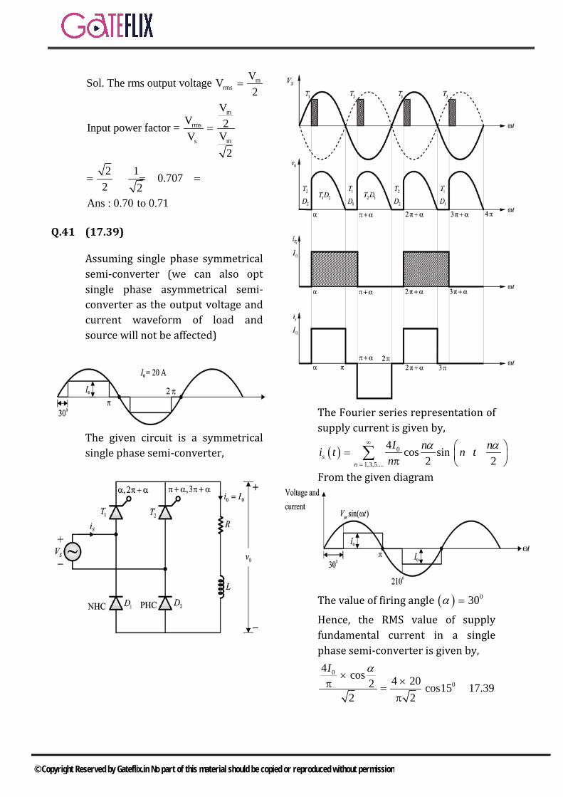
mrms
m
rms
ms
VSol. The rms output voltage V2
VV 2Input power factor =
VV2
2 1 0.7072 2
Ans : 0.70 to 0.71
=
=
= = =
Q.41 (17.39)
Assuming single phase symmetrical semi-converter (we can also opt single phase asymmetrical semi-converter as the output voltage and current waveform of load and source will not be affected)
The given circuit is a symmetrical single phase semi-converter,
The Fourier series representation of supply current is given by,
( ) 0
1,3,5....
4 cos sin2 2s
n
I n ni t n tn
α α∞
=
= ω − π ∑
From the given diagram
The value of firing angle ( ) 030α =
Hence, the RMS value of supply fundamental current in a single phase semi-converter is given by,
0
0
4 cos 4 202 cos15 17.392 2
I α× ×π = =
π
© Copyright Reserved by Gateflix.in No part of this material should be copied or reproduced without permission
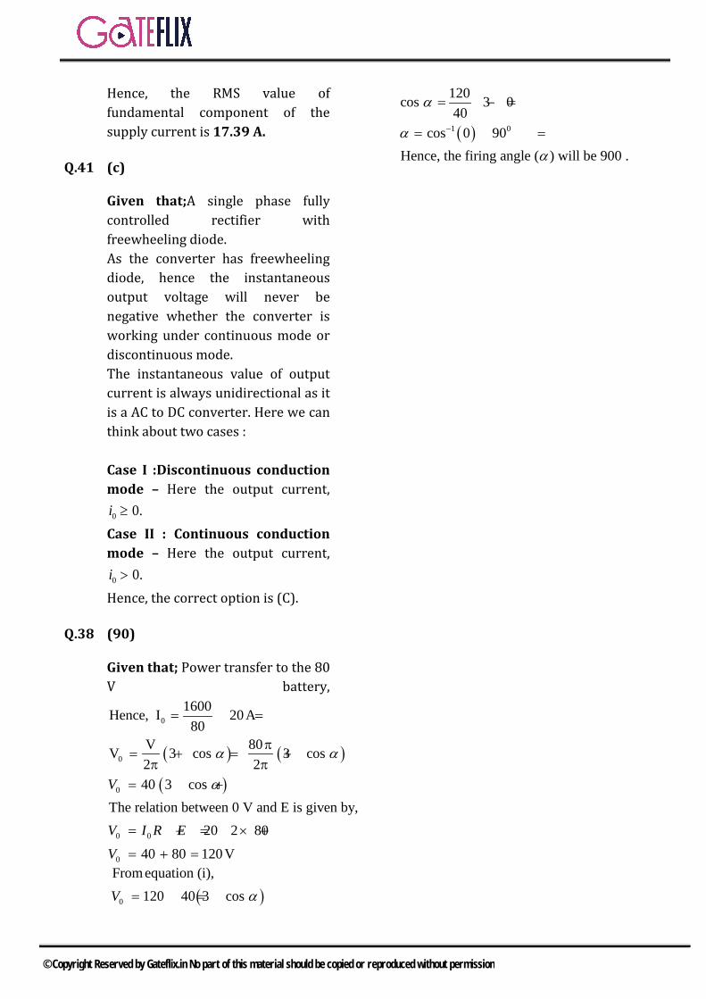
Hence, the RMS value of fundamental component of the supply current is 17.39 A.
Q.41 (c)
Given that;A single phase fully controlled rectifier with freewheeling diode. As the converter has freewheeling diode, hence the instantaneous output voltage will never be negative whether the converter is working under continuous mode or discontinuous mode. The instantaneous value of output current is always unidirectional as it is a AC to DC converter. Here we can think about two cases :
Case I :Discontinuous conduction mode – Here the output current,
0 0.i ≥ Case II : Continuous conduction mode – Here the output current,
0 0.i > Hence, the correct option is (C).
Q.38 (90)
Given that; Power transfer to the 80 V battery,
( ) ( )
( )
0
0
0
0 0
0
1600Hence, I 20A80
V 80V 3 cos 3 cos2 240 3 cos
The relation between 0 V and E is given by,20 2 80
40 80 120V
V
V I R EV
α α
α
= =
π= + = +
π π= +
= + = × +
= + =
( )0
From equation (i),120 40 3 cosV α= = +
( )1 0
120cos 3 040
cos 0 90Hence, the firing angle ( ) will be 900 .
α
αα
−
= − =
= =
© Copyright Reserved by Gateflix.in No part of this material should be copied or reproduced without permission
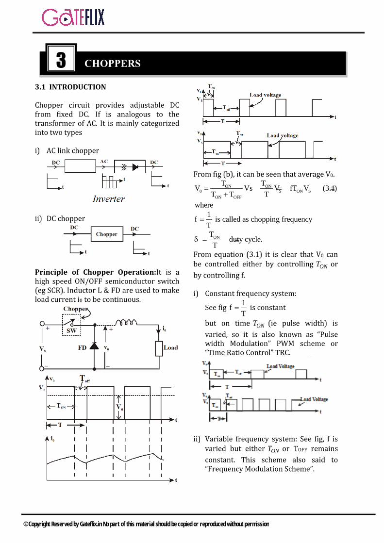
3.1 INTRODUCTION
Chopper circuit provides adjustable DC from fixed DC. If is analogous to the transformer of AC. It is mainly categorized into two types
i) AC link chopper
ii) DC chopper
Principle of Chopper Operation:It is a high speed ON/OFF semiconductor switch (eg SCR). Inductor L & FD are used to make load current i0 to be continuous.
From fig (b), it can be seen that average V0. ON ON
0 S ON SON OFF
T TV Vs V fT V (3.1)T T T
= = = − −+
where 1f is called as chopping frequencyT
=
ONT duty cycle.T
δ = =
From equation (3.1) it is clear that V0 can be controlled either by controlling ONT or by controlling f.
i) Constant frequency system:
See fig 1fT
= is constant
but on time ONT (ie pulse width) isvaried, so it is also known as “Pulsewidth Modulation” PWM scheme or“Time Ratio Control” TRC.
ii) Variable frequency system: See fig, f isvaried but either ONT or TOFF remainsconstant. This scheme also said to“Frequency Modulation Scheme”.
3 CHOPPERS
© Copyright Reserved by Gateflix.in No part of this material should be copied or reproduced without permission
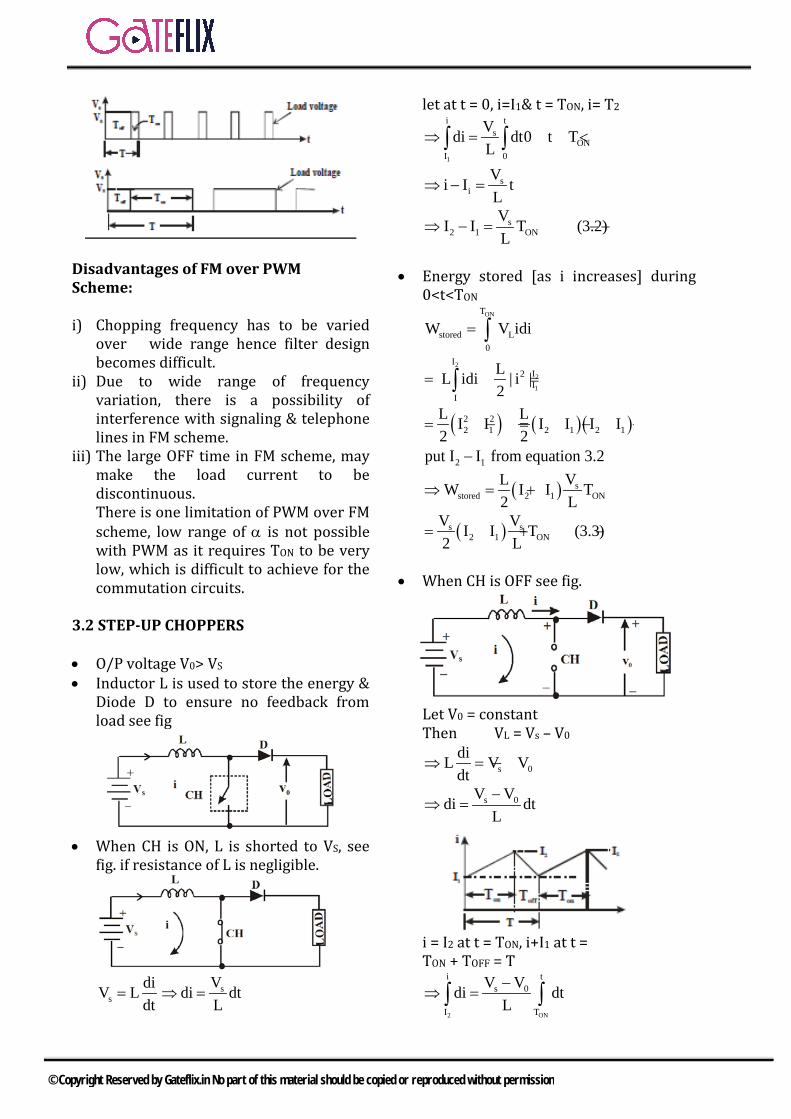
Disadvantages of FM over PWM Scheme:
i) Chopping frequency has to be variedover wide range hence filter designbecomes difficult.
ii) Due to wide range of frequencyvariation, there is a possibility ofinterference with signaling & telephonelines in FM scheme.
iii) The large OFF time in FM scheme, maymake the load current to bediscontinuous.There is one limitation of PWM over FMscheme, low range of α is not possiblewith PWM as it requires TON to be verylow, which is difficult to achieve for thecommutation circuits.
3.2 STEP-UP CHOPPERS
• O/P voltage V0> VS
• Inductor L is used to store the energy &Diode D to ensure no feedback fromload see fig
• When CH is ON, L is shorted to VS, seefig. if resistance of L is negligible.
sdiV Ldt
= sVdi dtL
⇒ =
let at t = 0, i=I1& t = TON, i= T2
1
i ts
ONI 0
Vdi dt0 t TL
⇒ = < ≤∫ ∫s
iVi I tL
⇒ − =
s2 1 ON
VI I T (3.2)L
⇒ − = −− −
• Energy stored [as i increases] during0<t<TON
ONT
stored L0
W V idi= ∫2
2
1
II2I
I
L L idi | i |2
= =∫
( ) ( )( )2 22 1 2 1 2 1
L LI I I I I I2 2
= − = − +
2 1put I I from equation 3.2−
( ) sstored 2 1 ON
VLW I I T2 L
⇒ = +
( )s s2 1 ON
V VI I T (3.3)2 L
= + − −
• When CH is OFF see fig.
Let V0 = constant Then VL = Vs – V0
s 0diL V Vdt
⇒ = −
s 0V Vdi dtL−
⇒ =
i = I2 at t = TON, i+I1 at t = TON + TOFF = T
2 ON
i ts 0
I T
V Vdi dtL−
⇒ =∫ ∫
© Copyright Reserved by Gateflix.in No part of this material should be copied or reproduced without permission
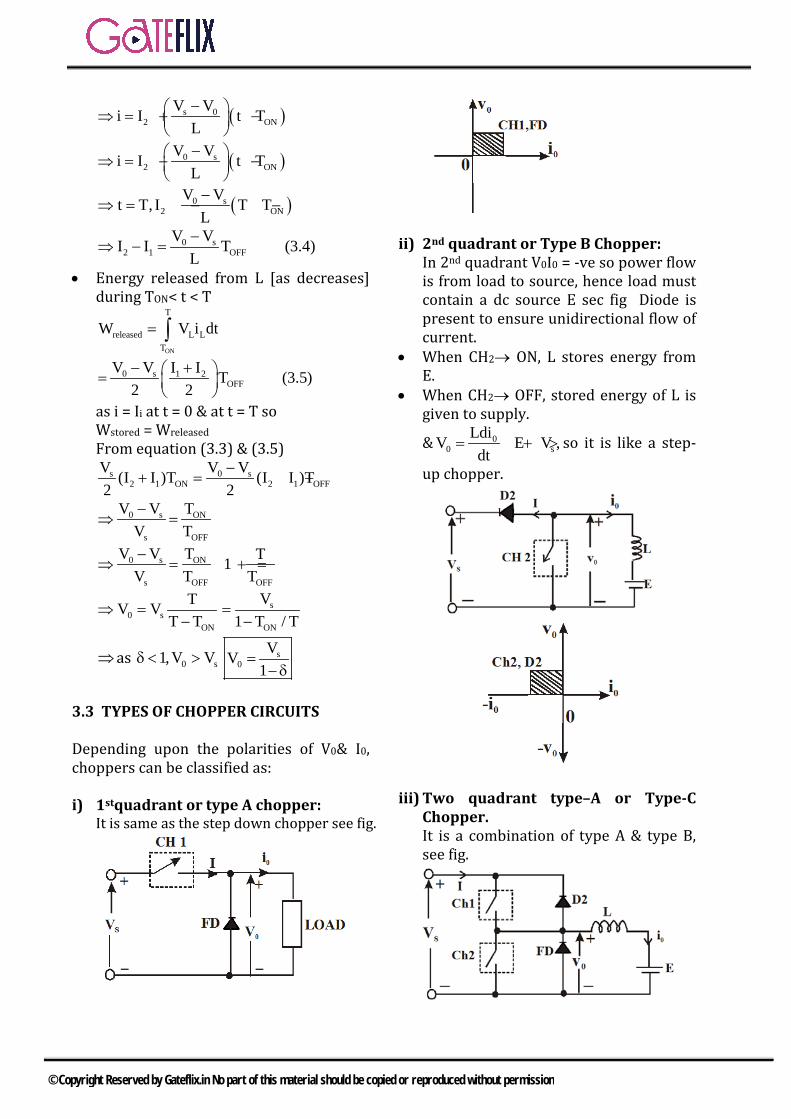
( )s 02 ON
V Vi I t TL− ⇒ = + −
( )0 s2 ON
V Vi I t TL− ⇒ = − −
( )0 s2 ON
V Vt T, I T TL−
⇒ = − −
0 s2 1 OFF
V VI I T (3.4)L−
⇒ − = − − −
• Energy released from L [as decreases]during TON< t < T
ON
T
released L LT
W V i dt= ∫
0 s 1 2OFF
V V I I T (3.5)2 2− + = − − −
as i = Ii at t = 0 & at t = T so Wstored = Wreleased From equation (3.3) & (3.5)
s 0 s2 1 ON 2 1 OFF
V V V(I I )T (I I )T2 2
−+ = +
0 s ON
s OFF
V V TV T−
⇒ =
0 s ON
s OFF OFF
V V T T1V T T−
⇒ = + =
0 sON
TV VT T
⇒ =−
s
ON
V1 T / T
=−
⇒as 0 s1,V Vδ < > s0
VV1
=−δ
3.3 TYPES OF CHOPPER CIRCUITS
Depending upon the polarities of V0& I0, choppers can be classified as:
i) 1stquadrant or type A chopper:It is same as the step down chopper see fig.
ii) 2nd quadrant or Type B Chopper:In 2nd quadrant V0I0 = -ve so power flowis from load to source, hence load mustcontain a dc source E sec fig Diode ispresent to ensure unidirectional flow ofcurrent.
• When CH2→ ON, L stores energy fromE.
• When CH2→ OFF, stored energy of L isgiven to supply.
& 00 s
LdiV E V ,dt
= + > so it is like a step-
up chopper.
iii) Two quadrant type–A or Type-CChopper.It is a combination of type A & type B,see fig.
© Copyright Reserved by Gateflix.in No part of this material should be copied or reproduced without permission
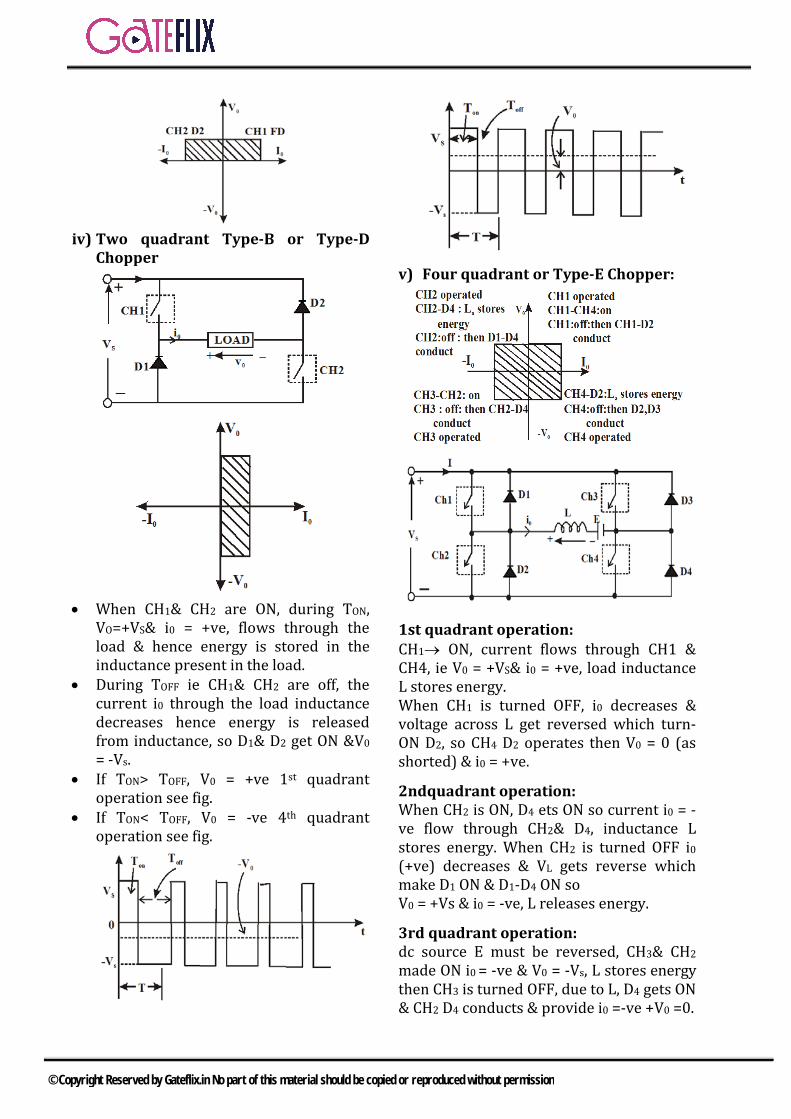
iv) Two quadrant Type-B or Type-DChopper
• When CH1& CH2 are ON, during TON,VO=+VS& i0 = +ve, flows through theload & hence energy is stored in theinductance present in the load.
• During TOFF ie CH1& CH2 are off, thecurrent i0 through the load inductancedecreases hence energy is releasedfrom inductance, so D1& D2 get ON &V0
= -Vs.• If TON> TOFF, V0 = +ve 1st quadrant
operation see fig.• If TON< TOFF, V0 = -ve 4th quadrant
operation see fig.
v) Four quadrant or Type-E Chopper:
1st quadrant operation: CH1→ ON, current flows through CH1 & CH4, ie V0 = +VS& i0 = +ve, load inductance L stores energy. When CH1 is turned OFF, i0 decreases & voltage across L get reversed which turn-ON D2, so CH4 D2 operates then V0 = 0 (as shorted) & i0 = +ve.
2ndquadrant operation: When CH2 is ON, D4 ets ON so current i0 = -ve flow through CH2& D4, inductance L stores energy. When CH2 is turned OFF i0 (+ve) decreases & VL gets reverse which make D1 ON & D1-D4 ON so V0 = +Vs & i0 = -ve, L releases energy.
3rd quadrant operation: dc source E must be reversed, CH3& CH2 made ON i0 = -ve & V0 = -Vs, L stores energy then CH3 is turned OFF, due to L, D4 gets ON & CH2 D4 conducts & provide i0 =-ve +V0 =0.
© Copyright Reserved by Gateflix.in No part of this material should be copied or reproduced without permission
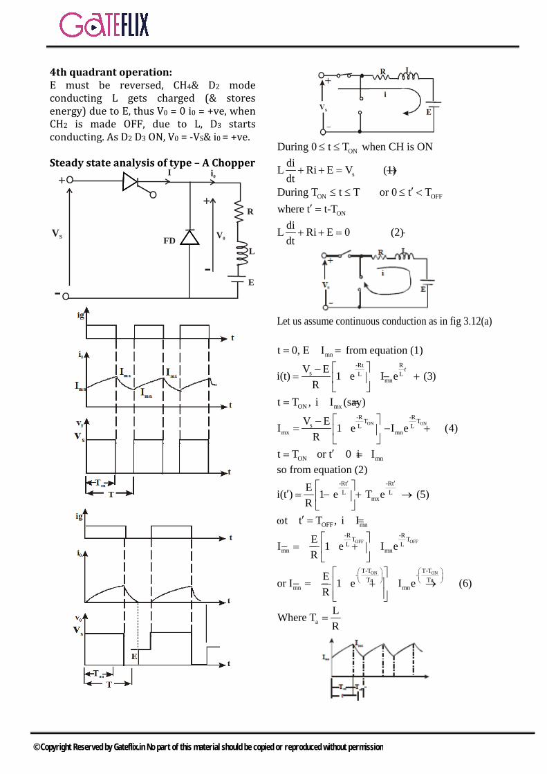
4th quadrant operation: E must be reversed, CH4& D2 mode conducting L gets charged (& stores energy) due to E, thus V0 = 0 i0 = +ve, when CH2 is made OFF, due to L, D3 starts conducting. As D2 D3 ON, V0 = -VS& i0 = +ve.
Steady state analysis of type – A Chopper ONDuring 0 t T when CH is ON≤ ≤
sdiL Ri E V (1)dt+ + = →
ON OFFDuring T t T or 0 t T′≤ ≤ ≤ <
ONwhere t t-T′ =diL Ri E 0 (2)dt+ + = →
Let us assume continuous conduction as in fig 3.12(a)
mnt 0, E I from equation (1)= =-Rt R
s L Lmn
V Ei(t) 1 e I e (3)R
−= − + − −
t
ON mxt T , i I (say)= =
ON ON-R -RT Ts L L
mx mnV EI 1 e I e (4)
R −
= − + − −
ON mnt T or t 0 i I′= = =so from equation (2)
-Rt -RtL L
mxEi(t ) 1 e T e (5)R
′ ′ ′ = − + →
OFF mnt t T , i I′ω = =
OFF OFF-R -RT TL L
mn mnEI 1 e I eR
= − − +
ON ONT-T T-T- -Ta Ta
mn mnEor I 1 e I e (6)R
= − − + →
aLWhere TR
=
+
-
+
-
VS
R
L
E
I i0
FD V0
© Copyright Reserved by Gateflix.in No part of this material should be copied or reproduced without permission
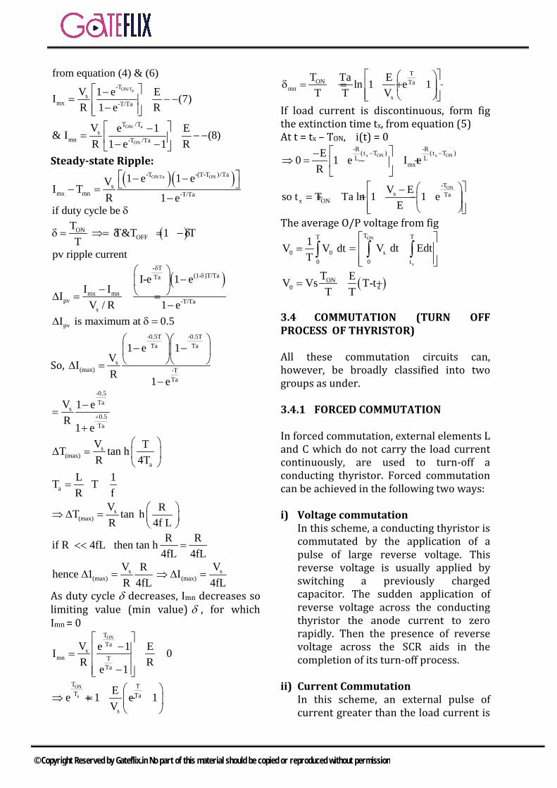
from equation (4) & (6)ON/Ta-T
smx -T/Ta
V 1 e EI (7)R 1 e R −
= − − − −
ON/ a
ON
T /Ts
mn -T /Ta
V e 1 E& I (8)R 1 e 1 R −
= − − − − − Steady-state Ripple:
( )( )ON/Ta ON-T -(T-T )/Ta
smx mn -T/Ta
1 e 1 eVI TR 1 e
− − − =−
if duty cycle be δ
( )ONOFF
T T&T 1 TT
δ = ⇒= δ = −δ
pv ripple current
( )- T
(1- )T/TaTa
mx mnpv -T/Ta
s
I-e 1 eI IIV / R 1 e
δδ
− − ∆ = =
−
pvI is maximum at 0.5∆ δ =
So,
-0.5T -0.5TTa Ta
s(max) -T
Ta
1 e 1VIR 1 e
− −
∆ =−
-0.5Ta
s0.5Ta
V 1 eR 1 e
+
−=
+
s(max)
a
V TT tan hR 4T
∆ =
aL 1T TR f
= =
s(max)
V RT tan hR 4f L
⇒ ∆ =
R Rif R 4fL then tan h4fL 4fL
<< =
s(max)
V Rhence 1R 4fL
∆ = s(max)
VI4fL
⇒∆ =
As duty cycle δ decreases, Imn decreases so limiting value (min value) δ , for which Imn = 0
ONTTa
smn T
Ta
V e 1 EI 0R Re 1
− = − = −
ON
a
T TT Ta
s
Ee 1 e 1V
⇒ = + −
TON Ta
mns
T Ta Eln 1 e 1T T V
δ = = + −
If load current is discontinuous, form fig the extinction time tx, from equation (5) At t = tx – TON, i(t) = 0
x ON x ON-R -R(t T ) (t T )L L
mxE0 1 e I e
R− − −
⇒ = − +
ON-Ts Ta
x ONV Eso t T Ta ln 1 1 e
E −
= + + −
The average O/P voltage from fig T
0 00
1V V dtT
= ∫ON
x
T T
s0 t
V dt Edt
= + ∫ ∫
( )ON0 x
T EV Vs T-tT T
= +
3.4 COMMUTATION (TURN OFF PROCESS OF THYRISTOR)
All these commutation circuits can, however, be broadly classified into two groups as under.
3.4.1 FORCED COMMUTATION
In forced commutation, external elements L and C which do not carry the load current continuously, are used to turn-off a conducting thyristor. Forced commutation can be achieved in the following two ways:
i) Voltage commutationIn this scheme, a conducting thyristor iscommutated by the application of apulse of large reverse voltage. Thisreverse voltage is usually applied byswitching a previously chargedcapacitor. The sudden application ofreverse voltage across the conductingthyristor the anode current to zerorapidly. Then the presence of reversevoltage across the SCR aids in thecompletion of its turn-off process.
ii) Current CommutationIn this scheme, an external pulse ofcurrent greater than the load current is
© Copyright Reserved by Gateflix.in No part of this material should be copied or reproduced without permission
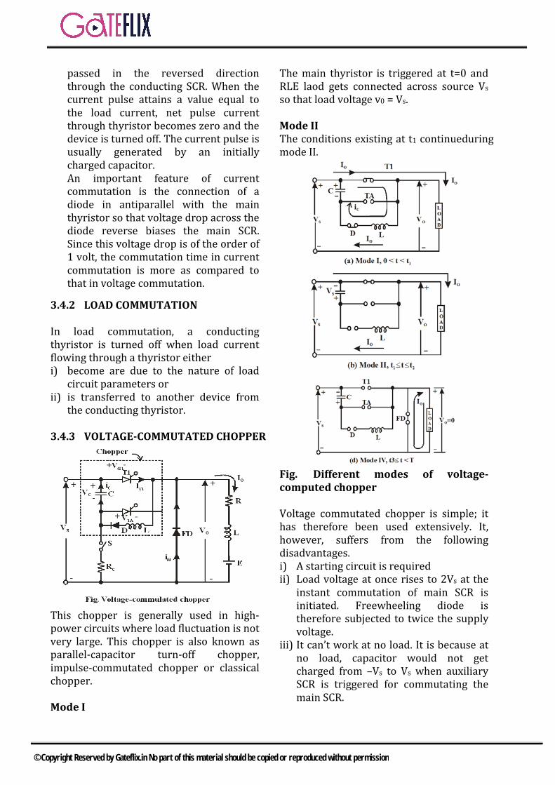
passed in the reversed direction through the conducting SCR. When the current pulse attains a value equal to the load current, net pulse current through thyristor becomes zero and the device is turned off. The current pulse is usually generated by an initially charged capacitor. An important feature of current commutation is the connection of a diode in antiparallel with the main thyristor so that voltage drop across the diode reverse biases the main SCR. Since this voltage drop is of the order of 1 volt, the commutation time in current commutation is more as compared to that in voltage commutation.
3.4.2 LOAD COMMUTATION
In load commutation, a conducting thyristor is turned off when load current flowing through a thyristor either i) become are due to the nature of load
circuit parameters orii) is transferred to another device from
the conducting thyristor.
3.4.3 VOLTAGE-COMMUTATED CHOPPER
This chopper is generally used in high-power circuits where load fluctuation is not very large. This chopper is also known as parallel-capacitor turn-off chopper, impulse-commutated chopper or classical chopper.
Mode I
The main thyristor is triggered at t=0 and RLE laod gets connected across source Vs so that load voltage v0 = Vs.
Mode II The conditions existing at t1 continueduring mode II.
Fig. Different modes of voltage-computed chopper
Voltage commutated chopper is simple; it has therefore been used extensively. It, however, suffers from the following disadvantages. i) A starting circuit is requiredii) Load voltage at once rises to 2Vs at the
instant commutation of main SCR isinitiated. Freewheeling diode istherefore subjected to twice the supplyvoltage.
iii) It can’t work at no load. It is because atno load, capacitor would not getcharged from –Vs to Vs when auxiliarySCR is triggered for commutating themain SCR.
© Copyright Reserved by Gateflix.in No part of this material should be copied or reproduced without permission
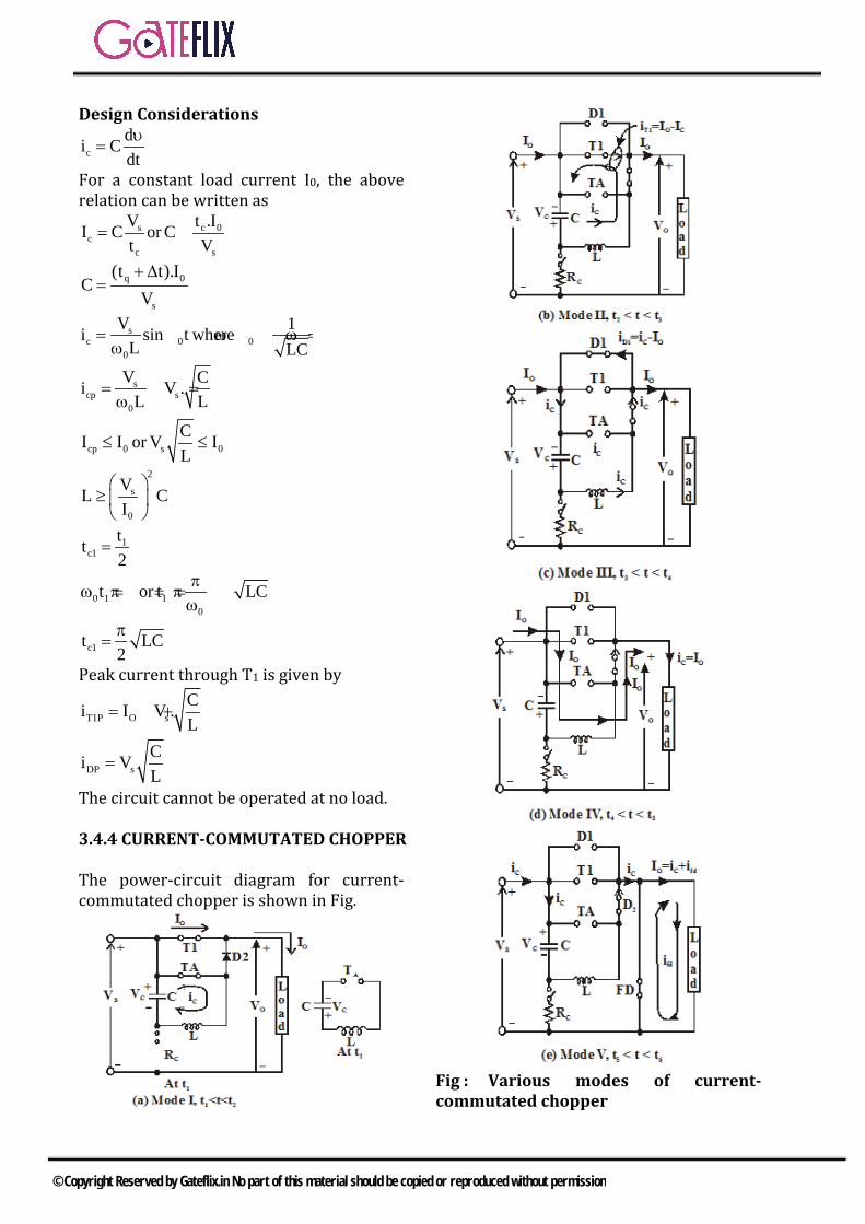
Design Considerations
cdi Cdtυ
=
For a constant load current I0, the above relation can be written as
s c 0c
c s
V t .II C or Ct V
= =
q 0
s
(t t).IC
V+ ∆
=
sc 0 0
0
V 1i sin t whereL LC
= ω ω =ω
scp s
0
V Ci V .L L
= =ω
cp 0 s 0CI I or V IL
≤ ≤
2
s
0
VL CI
≥
1c1
tt2
=
0 1 10
t or t LCπω = π = = π
ω
c1t LC2π
=
Peak current through T1 is given by
T1P O sCi I V .L
= +
DP sCi VL
=
The circuit cannot be operated at no load.
3.4.4 CURRENT-COMMUTATED CHOPPER
The power-circuit diagram for current-commutated chopper is shown in Fig.
Fig : Various modes of current-commutated chopper
© Copyright Reserved by Gateflix.in No part of this material should be copied or reproduced without permission
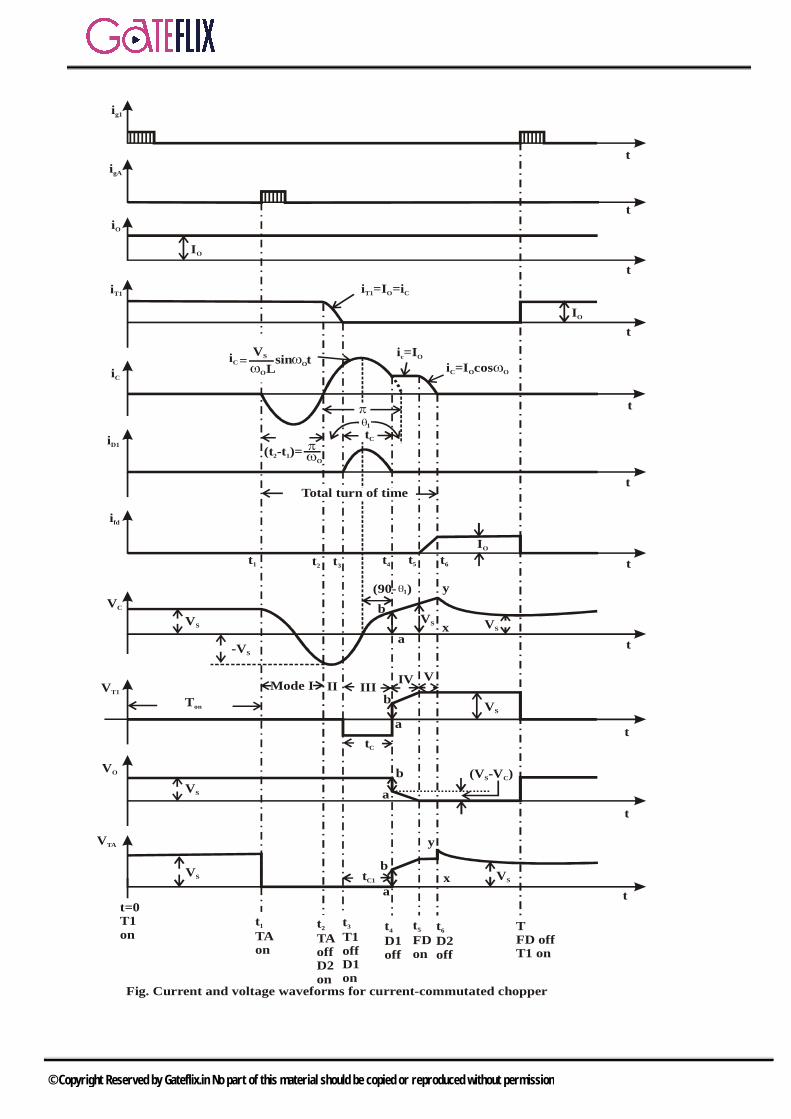
ig1
t
t
t
t
t
t
t
t
t
igA
iO
iC
iT1
ifd
VC
VT1
t
t
VTA
VO
iD1
IO
IO
i =I =iT1 O C
iCVS sin t
LO= O
i =Ic O
i =I cos C O O
tC
1
(t -t )=2 1O
Total turn of time
IO
t1 t2 t3 t4 t5 t6
(90- )1
a
b
-VS
VS x
y
VS
Mode I II III IV V
Ton
a
b
tC
VS
VS
VS a
b (V -V )S C
VS tC1
a
bx
y
VS
t=0T1on
tTAon
1 tTAoffD2on
2 tT1offD1on
3 tD1off
4 tFDon
5 tD2off
6 TFD offT1 on
Fig. Current and voltage waveforms for current-commutated chopper
© Copyright Reserved by Gateflix.in No part of this material should be copied or reproduced without permission
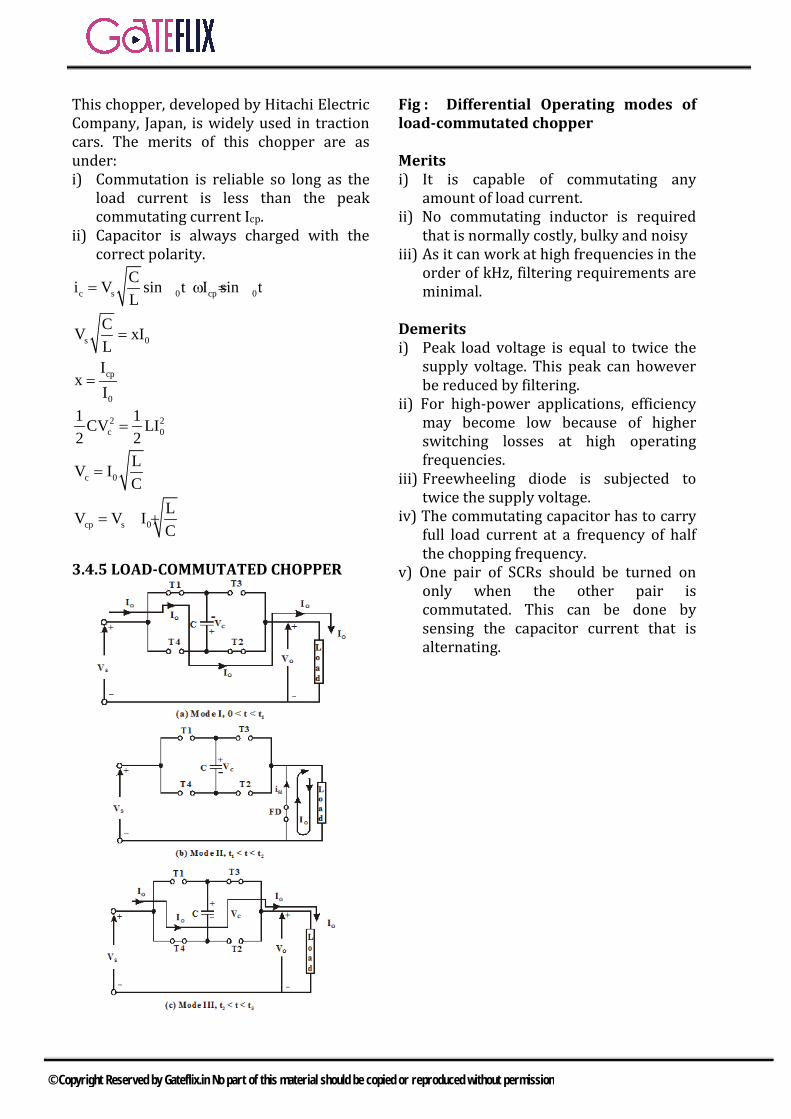
This chopper, developed by Hitachi Electric Company, Japan, is widely used in traction cars. The merits of this chopper are as under: i) Commutation is reliable so long as the
load current is less than the peakcommutating current Icp.
ii) Capacitor is always charged with thecorrect polarity.
c s 0 cp 0Ci V sin t I sin tL
= ω = ω
s 0CV xIL=
cp
0
Ix
I=
2 2c 0
1 1CV LI2 2
=
c 0LV IC
=
cp s 0LV V IC
= +
3.4.5 LOAD-COMMUTATED CHOPPER
Fig : Differential Operating modes of load-commutated chopper
Merits i) It is capable of commutating any
amount of load current.ii) No commutating inductor is required
that is normally costly, bulky and noisyiii) As it can work at high frequencies in the
order of kHz, filtering requirements areminimal.
Demerits i) Peak load voltage is equal to twice the
supply voltage. This peak can howeverbe reduced by filtering.
ii) For high-power applications, efficiencymay become low because of higherswitching losses at high operatingfrequencies.
iii) Freewheeling diode is subjected totwice the supply voltage.
iv) The commutating capacitor has to carryfull load current at a frequency of halfthe chopping frequency.
v) One pair of SCRs should be turned ononly when the other pair iscommutated. This can be done bysensing the capacitor current that isalternating.
© Copyright Reserved by Gateflix.in No part of this material should be copied or reproduced without permission
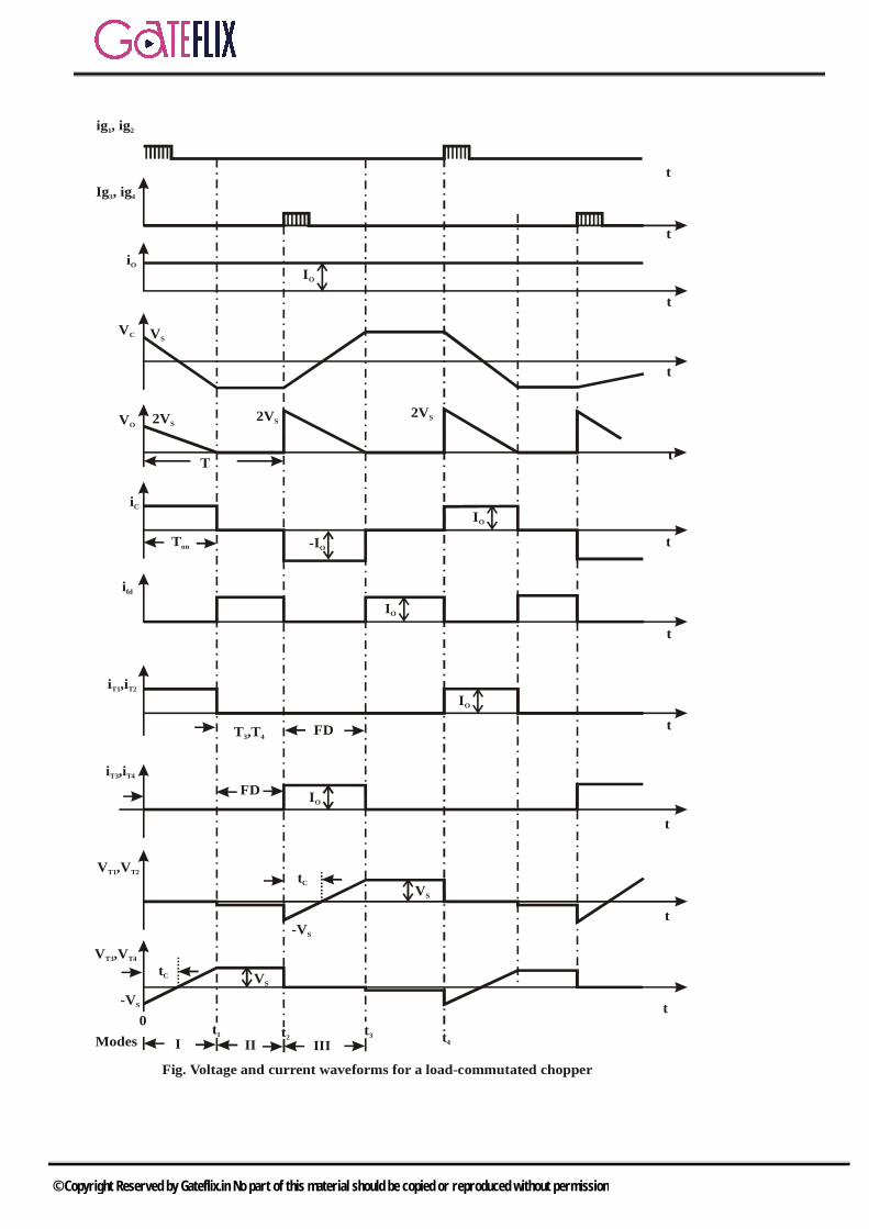
t
t
t
t
t
t
t
t
t
t
t
ig , ig1 2
Ig , ig3 4
VC
iO
VS
IO
VO 2VS2VS
2VS
T
IO
Ton -IO
iC
ifd
IO
IO
i ,iT1 T2
T ,T3 4 FD
i ,iT3 T4
FD IO
V ,VT1 T2 tCVS
-VS
V ,VT3 T4
tC VS
-VS
0 t1 t2t3 t4Modes I II III
Fig. Voltage and current waveforms for a load-commutated chopper
© Copyright Reserved by Gateflix.in No part of this material should be copied or reproduced without permission
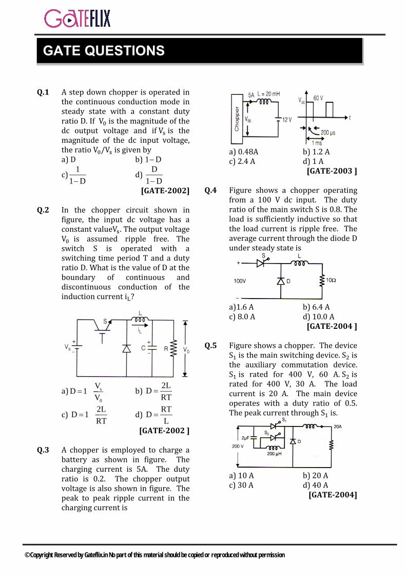
Q.1 A step down chopper is operated in the continuous conduction mode in steady state with a constant duty ratio D. If V0 is the magnitude of the dc output voltage and if Vs is the magnitude of the dc input voltage, the ratio V0/Vs is given by a) D b) 1 D−
c)1
1 D−d)
D1 D−
[GATE-2002]
Q.2 In the chopper circuit shown in figure, the input dc voltage has a constant valueVs. The output voltage V0 is assumed ripple free. The switch S is operated with a switching time period T and a duty ratio D. What is the value of D at the boundary of continuous and discontinuous conduction of the induction current iL?
a) s
0
VD 1V
= − b)2LDRT
=
c) 2LD 1RT
= − d) RTDL
=
[GATE-2002 ]
Q.3 A chopper is employed to charge a battery as shown in figure. The charging current is 5A. The duty ratio is 0.2. The chopper output voltage is also shown in figure. The peak to peak ripple current in the charging current is
a) 0.48A b) 1.2 Ac) 2.4 A d) 1 A
[GATE-2003 ]
Q.4 Figure shows a chopper operating from a 100 V dc input. The duty ratio of the main switch S is 0.8. The load is sufficiently inductive so that the load current is ripple free. The average current through the diode D under steady state is
a)1.6 A b) 6.4 Ac) 8.0 A d) 10.0 A
[GATE-2004 ]
Q.5 Figure shows a chopper. The device S1 is the main switching device. S2 is the auxiliary commutation device. S1 is rated for 400 V, 60 A. S2 is rated for 400 V, 30 A. The load current is 20 A. The main device operates with a duty ratio of 0.5. The peak current through S1 is.
a) 10 A b) 20 Ac) 30 A d) 40 A
[GATE-2004]
GATE QUESTIONS
© Copyright Reserved by Gateflix.in No part of this material should be copied or reproduced without permission
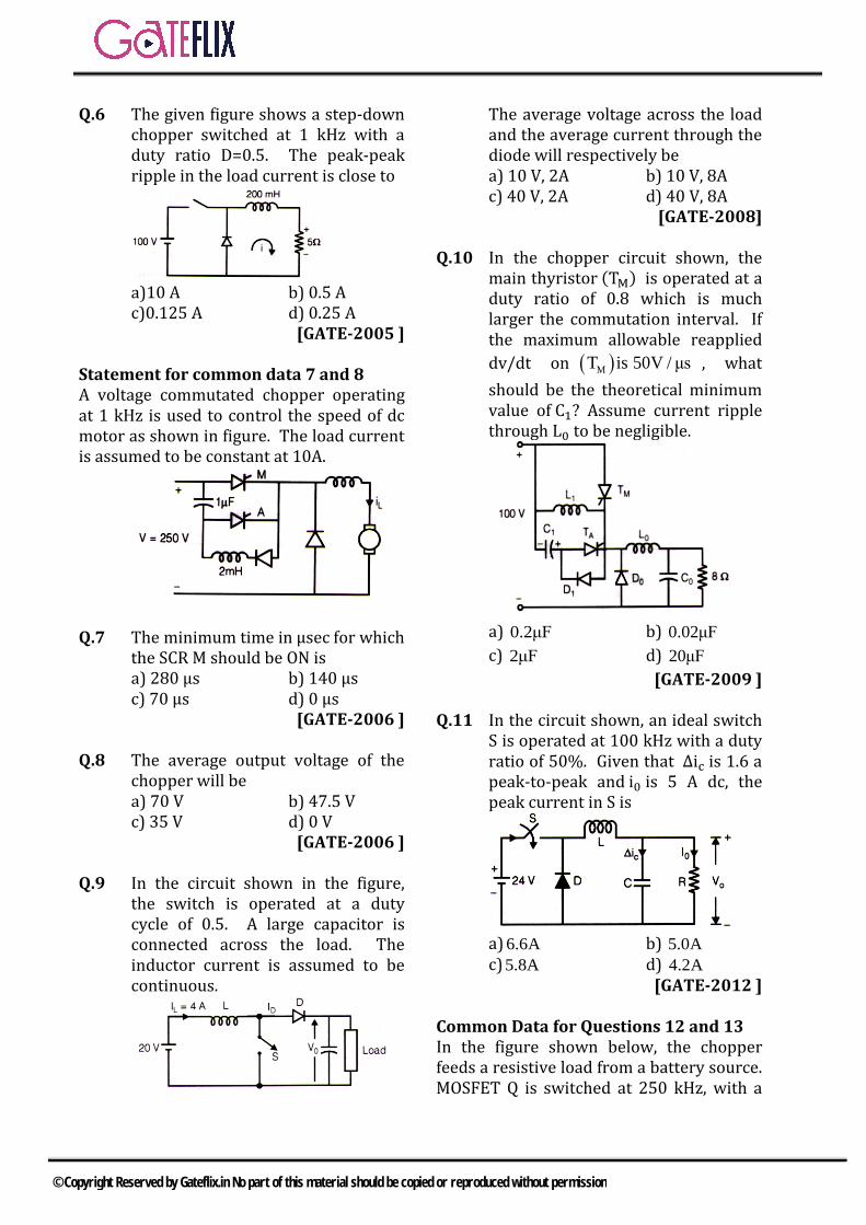
Q.6 The given figure shows a step-down chopper switched at 1 kHz with a duty ratio D=0.5. The peak-peak ripple in the load current is close to
a)10 A b) 0.5 Ac)0.125 A d) 0.25 A
[GATE-2005 ]
Statement for common data 7 and 8 A voltage commutated chopper operating at 1 kHz is used to control the speed of dc motor as shown in figure. The load current is assumed to be constant at 10A.
Q.7 The minimum time in µsec for which the SCR M should be ON is a) 280 μs b) 140 μsc) 70 μs d) 0 μs
[GATE-2006 ]
Q.8 The average output voltage of the chopper will be a) 70 V b) 47.5 Vc) 35 V d) 0 V
[GATE-2006 ]
Q.9 In the circuit shown in the figure, the switch is operated at a duty cycle of 0.5. A large capacitor is connected across the load. The inductor current is assumed to be continuous.
The average voltage across the load and the average current through the diode will respectively be a) 10 V, 2A b) 10 V, 8Ac) 40 V, 2A d) 40 V, 8A
[GATE-2008]
Q.10 In the chopper circuit shown, the main thyristor (TM) is operated at a duty ratio of 0.8 which is much larger the commutation interval. If the maximum allowable reapplied dv/dt on ( )MT is 50V / μs , what should be the theoretical minimum value of C1? Assume current ripple through L0 to be negligible.
a) 0.2μF b) 0.02μFc) 2μF d) 20μF
[GATE-2009 ]
Q.11 In the circuit shown, an ideal switch S is operated at 100 kHz with a duty ratio of 50%. Given that ∆ic is 1.6 a peak-to-peak and i0 is 5 A dc, the peak current in S is
a) 6.6A b) 5.0Ac) 5.8A d) 4.2A
[GATE-2012 ]
Common Data for Questions 12 and 13 In the figure shown below, the chopper feeds a resistive load from a battery source. MOSFET Q is switched at 250 kHz, with a
© Copyright Reserved by Gateflix.in No part of this material should be copied or reproduced without permission
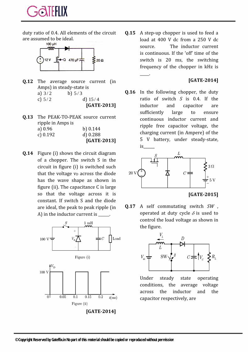
duty ratio of 0.4. All elements of the circuit are assumed to be ideal.
Q.12 The average source current (in
Amps) in steady-state is a) 3 / 2 b) 5 / 3 c) 5 / 2 d) 15 / 4
[GATE-2013]
Q.13 The PEAK-TO-PEAK source current ripple in Amps is
a) 0.96 b) 0.144 c) 0.192 d) 0.288
[GATE-2013] Q.14 Figure (i) shows the circuit diagram
of a chopper. The switch S in the circuit in figure (i) is switched such that the voltage vD across the diode has the wave shape as shown in figure (ii). The capacitance C is large so that the voltage across it is constant. If switch S and the diode are ideal, the peak to peak ripple (in A) in the inductor current is ______.
[GATE-2014]
Q.15 A step-up chopper is used to feed a load at 400 V dc from a 250 V dc source. The inductor current is continuous. If the ‘off’ time of the switch is 20 ms, the switching frequency of the chopper in kHz is _____.
[GATE-2014] Q.16 In the following chopper, the duty
ratio of switch S is 0.4. If the inductor and capacitor are sufficiently large to ensure continuous inductor current and ripple free capacitor voltage, the charging current (in Ampere) of the 5 V battery, under steady-state, is______
[GATE-2015]
Q.17 A self commutating switch SW ,
operated at duty cycle δ is used to control the load voltage as shown in the figure.
Under steady state operating conditions, the average voltage across the inductor and the capacitor respectively, are
© Copyright Reserved by Gateflix.in No part of this material should be copied or reproduced without permission
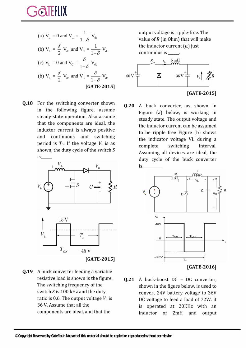
L C dc
L dc C dc
L C dc
L dc C dc
1(a) V = 0 and V = V1
1(b) V = V and V = V2 1
(c) V = 0 and V = V1
(b) V = V and V = V2 1
δδ
δδδ
δ δδ
−
−
−
−[GATE-2015]
Q.18 For the switching converter shown in the following figure, assume steady-state operation. Also assume that the components are ideal, the inductor current is always positive and continuous and switching period is T5. If the voltage VL is as shown, the duty cycle of the switch S is______
[GATE-2015]
Q.19 A buck converter feeding a variable resistive load is shown is the figure. The switching frequency of the switch S is 100 kHz and the duty ratio is 0.6. The output voltage V0 is 36 V. Assume that all the components are ideal, and that the
output voltage is ripple-free. The value of R (in Ohm) that will make the inductor current (iL) just continuous is ______.
[GATE-2015]
Q.20 A buck converter, as shown in Figure (a) below, is working in steady state. The output voltage and the inductor current can be assumed to be ripple free Figure (b) shows the indicator voltage VL during a complete switching interval. Assuming all devices are ideal, the duty cycle of the buck converter is___________.
[GATE-2016]
Q.21 A buck-boost DC – DC converter, shown in the figure below, is used to convert 24V battery voltage to 36V DC voltage to feed a load of 72W. it is operated at 20KHz with an inductor of 2mH and output
© Copyright Reserved by Gateflix.in No part of this material should be copied or reproduced without permission
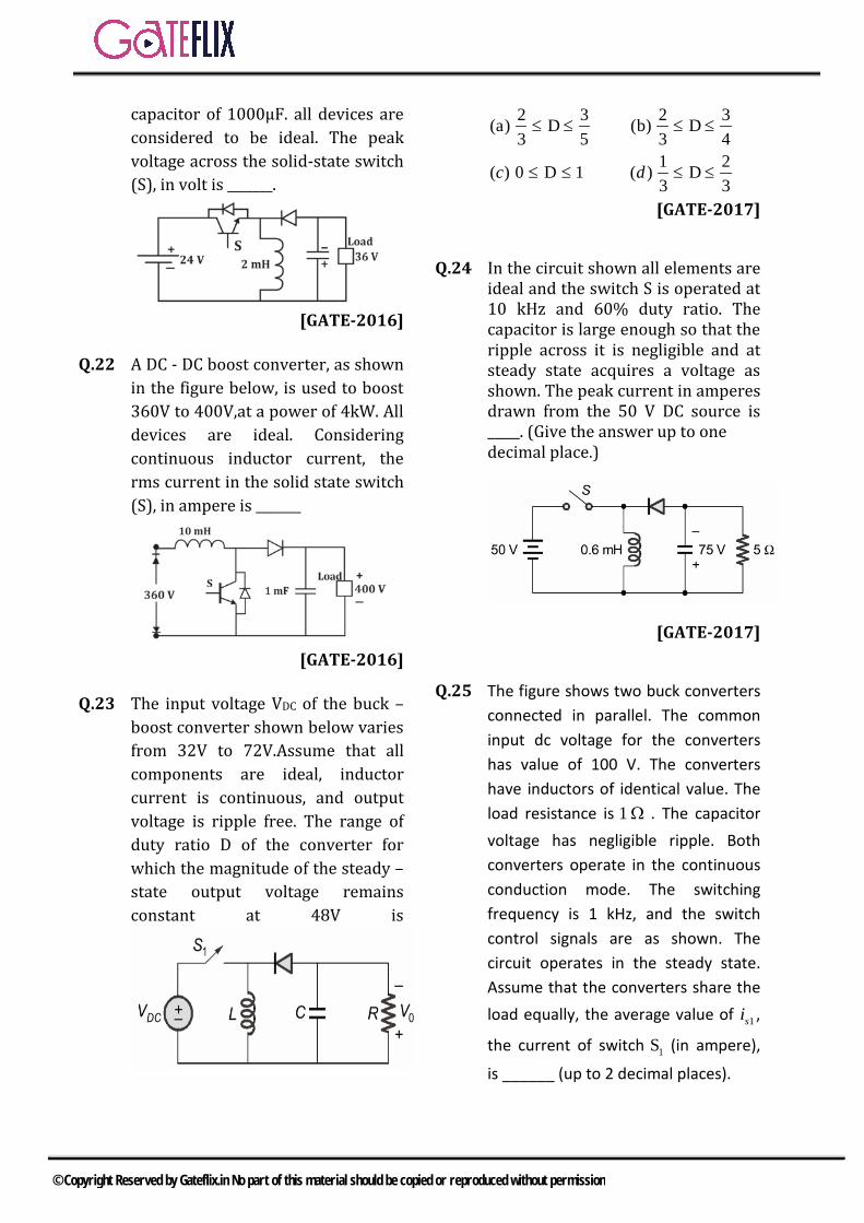
capacitor of 1000μF. all devices are considered to be ideal. The peak voltage across the solid-state switch (S), in volt is _______.
[GATE-2016]
Q.22 A DC - DC boost converter, as shown in the figure below, is used to boost 360V to 400V,at a power of 4kW. All devices are ideal. Considering continuous inductor current, the rms current in the solid state switch (S), in ampere is _______
[GATE-2016]
Q.23 The input voltage VDC of the buck – boost converter shown below varies from 32V to 72V.Assume that all components are ideal, inductor current is continuous, and output voltage is ripple free. The range of duty ratio D of the converter for which the magnitude of the steady –state output voltage remains constant at 48V is
2 3 2 3(a) D (b) D3 5 3 4
1 2( ) 0 D 1 ( ) D3 3
c d
≤ ≤ ≤ ≤
≤ ≤ ≤ ≤
[GATE-2017]
Q.24 In the circuit shown all elements are ideal and the switch S is operated at 10 kHz and 60% duty ratio. The capacitor is large enough so that the ripple across it is negligible and at steady state acquires a voltage as shown. The peak current in amperes drawn from the 50 V DC source is _____. (Give the answer up to one decimal place.)
[GATE-2017]
Q.25 The figure shows two buck converters connected in parallel. The common input dc voltage for the converters has value of 100 V. The converters have inductors of identical value. The load resistance is 1 Ω . The capacitor voltage has negligible ripple. Both converters operate in the continuous conduction mode. The switching frequency is 1 kHz, and the switch control signals are as shown. The circuit operates in the steady state. Assume that the converters share the load equally, the average value of 1si ,
the current of switch 1S (in ampere),
is ______ (up to 2 decimal places).
© Copyright Reserved by Gateflix.in No part of this material should be copied or reproduced without permission
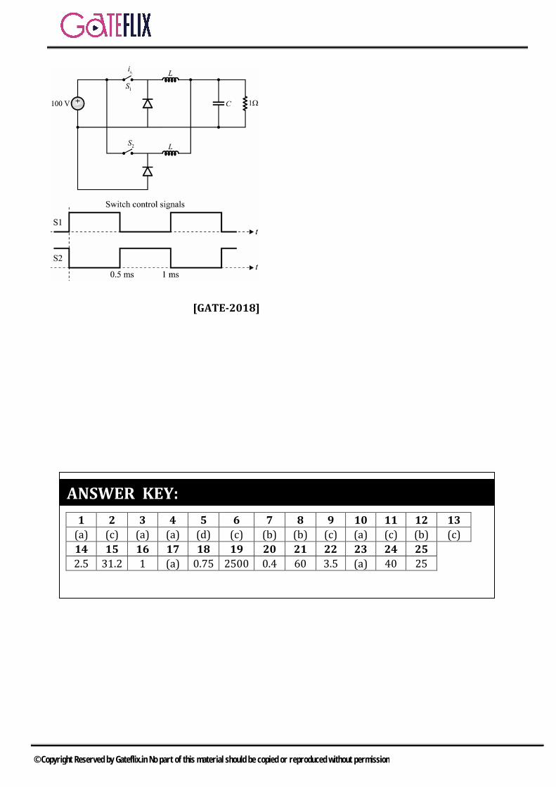
[GATE-2018]
1 2 3 4 5 6 7 8 9 10 11 12 13 (a) (c) (a) (a) (d) (c) (b) (b) (c) (a) (c) (b) (c) 14 15 16 17 18 19 20 21 22 23 24 25 2.5 31.2 1 (a) 0.75 2500 0.4 60 3.5 (a) 40 25
ANSWER KEY:
© Copyright Reserved by Gateflix.in No part of this material should be copied or reproduced without permission
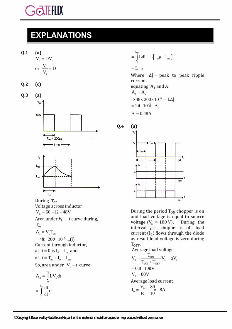
Q.1 (a) o sV DV=
or o
s
V DV
=
Q.2 (c)
Q.3 (a)
During Ton, Voltage across inductor
LV 60 12 48V= − −Area under VL − t curve during,
onT
1 L onA V T=648 200 10−= × × …(i)
Current through inductor, at 0 mnt 0 is I I= = and at on 0 mxt T is I I= =So, area under LV t− curve
onT
2 L0
A LV dt= ∫onT
0
di dtdt
= ∫
[ ]mxI
mx mn0
Ldi L I I= = −∫L= ∆
Where ∆| = peak to peak ripple current. equating A1 and A
1 2A A= ⇒ 648 200 10−× × = L∆|
320 10−= × ×∆
0.48A∆ =
Q.4 (a)
During the period TON chopper is on and load voltage is equal to source voltage (Vs = 100 V) . During the interval TOFF, chopper is off, load current (I0) flows through the diode as result load voltage is zero during TOFF. Average load voltage
ON0 s s
ON OFF
TV V αVT T
= =+
0.8 100V= ×0V 80V=
Average load current 0
0V 80I 8AR 10
= = =
EXPLANATIONS
© Copyright Reserved by Gateflix.in No part of this material should be copied or reproduced without permission
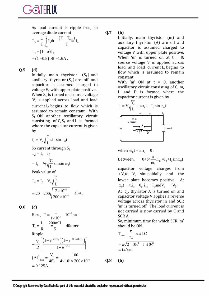
As load current is ripple free, so average diode current
( )ON
TON
D 0 0T
T T1I I dt IT T
−= =∫( )D 0I 1 α I= −
( )1 0.8 8 1.6A= − × = .
Q.5 (d) Initially main thyristor (S1) and auxiliary thyristor (S2) are off and capacitor is assumed charged to voltage Vs with upper plate positive. When S1 is turned on, source voltage
sV is applied across load and load current I0 begins to flow which is assumed to remain constant. With S1 ON another oscillatory circuit consisting of C, S1, and L is formed where the capacitor current is given by
c s 0Ci V sin sinω tL
=
So current through S1, s1 0 cI I i= +
0 s 0CI V sin sinω tL
= +
Peak value of
s1 0 sCI I VL
= +
6
6
2 1020 200 40A200 10
−
−
×= + =
×.
Q.6 (c)
Here, 33
1T 10 sec1 10
−= =×
aL 200mHT 40msecR 5
= = =
Ripple ( )( )a a
a
αT/T (1 α)T/Ts
T/T
1 e 1 eVR 1 e
− − −
−
− − =
−
( ) s3 3max
V 100I4fL 4 10 200 10−∆ = =
× × ×0.125A= .
Q.7 (b) Initially, main thyristor (m) and auxiliary thyristor (A) are off and capacitor is assumed charged to voltage V with upper plate positive. When ‘m’ is turned on at t = 0, source voltage V is applied across load and load current Io begins to flow which is assumed to remain constant. With ‘m’ ON at t = 0, another oscillatory circuit consisting of C, m, L and D is formed where the capacitor current is given by
c 0 p 0Ci V sinω t I sinω tL
= =
when 0 cω t π,i 0= = .
Between, T1 0 p 00
π0<t< ,i =I +I sinω tω
capacitor voltage charges from s sV to V+ − sinusoidally and the
lower plate becomes positive. At0 c i T1 0 c sω t π,i 0 , i I andV V= = = = − .
At t1, thyristor A is turned on and capacitor voltage V applies a reverse voltage across thyristor in and SCR ‘m’ is turned off. The load current is not carried is now carried by C and SCR A. So, minimum time for which SCR ‘m’ should be ON.
min0
πT = =π LCω
3 6π 2 10 1 10− −= × × ×140μs= .
Q.8 (b)
© Copyright Reserved by Gateflix.in No part of this material should be copied or reproduced without permission
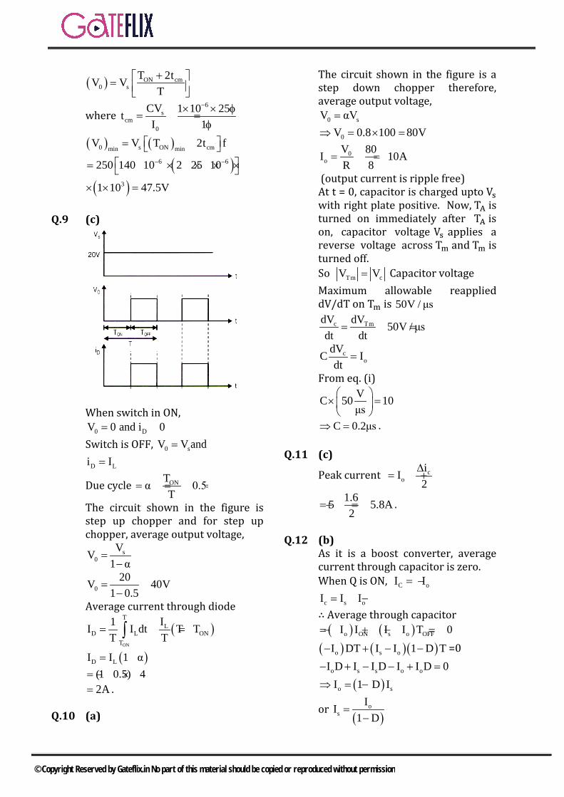
( ) ON cm0 s
T 2tV VT+ =
where 6
scm
0
CV 1 10 25tI 1
−× × φ= =
φ
( ) ( )0 s ON cmmin minV V T 2t f = +
( )( )
6 6
3
250 140 10 2 25 10
1 10 47.5V
− − = × × × ×
× × =
Q.9 (c)
When switch in ON, 0 DV 0 and i 0= =
Switch is OFF, 0 sV V and=
D Li I=
Due cycle ONTα 0.5T
= = =
The circuit shown in the figure is step up chopper and for step up chopper, average output voltage,
s0
VV1 α
=−
020V 40V
1 0.5= =
−Average current through diode
( )ON
TL
D L ONT
I1I I dt T TT T
= = −∫( )D LI I 1 α= −
(1 0.5) 4= − ×2A= .
Q.10 (a)
The circuit shown in the figure is a step down chopper therefore, average output voltage,
0 sV αV=
0V 0.8 100 80V⇒ = × =
0o
V 80I 10AR 8
= = =
(output current is ripple free) At t = 0, capacitor is charged upto Vs with right plate positive. Now, TA is turned on immediately after TA is on, capacitor voltage Vs applies a reverse voltage across Tm and Tm is turned off. So Tm cV V= Capacitor voltage Maximum allowable reapplied dV/dT on Tm is 50V / μs
c TmdV dV 50V / μsdt dt
= =
co
dVC Idt
=
From eq. (i) VC 50 10μs
× = C 0.2μs⇒ = .
Q.11 (c)
Peak current co
iI2∆
= +
1.65 5.8A2
= + = .
Q.12 (b) As it is a boost converter, average current through capacitor is zero. When Q is ON, C oI I= −
c s oI I I= −∴ Average through capacitor ( ) ( )o ON s o OFFI I I I T 0= − + − =
( ) ( )( )o s oI DT I I 1 D T− + − − =0
o s s o oI D I I D I I D 0− + − − + = ( )o sI 1 D I⇒ = −
or ( )
os
II1 D
=−
© Copyright Reserved by Gateflix.in No part of this material should be copied or reproduced without permission
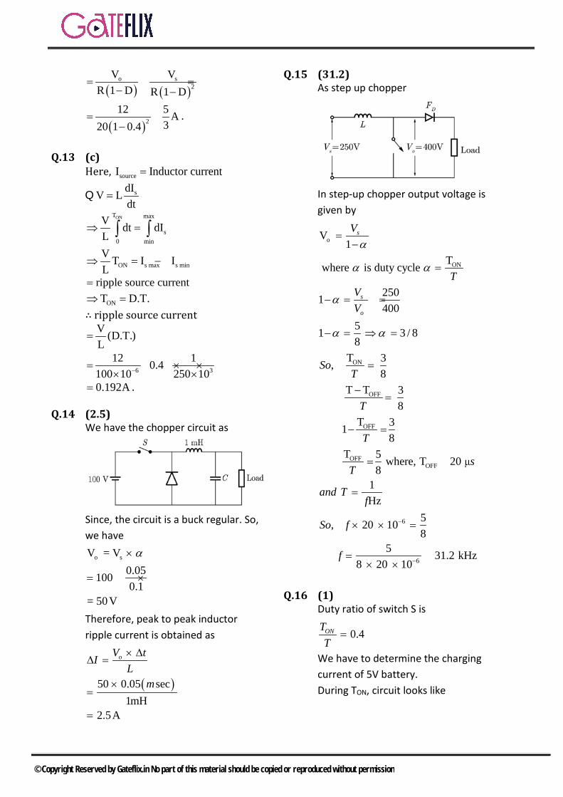
( ) ( )o s
2V V
R 1 D R 1 D= =
− −
( )212 5 A
320 1 0.4= =
−.
Q.13 (c) Here, sourceI Inductor current=
sdIV Ldt
=Q
ONT max
s0 min
V dt dIL
⇒ =∫ ∫
ON s max s minV T I IL
⇒ = −
ripple source current=
ONT D.T.⇒ =∴ ripple source current
V (D.T.)L
=
6 3
12 10.4100 10 250 10−= × ×
× ×0.192A= .
Q.14 (2.5) We have the chopper circuit as
Since, the circuit is a buck regular. So, we have
o sV = V 0.051000.1
= 50V
α×
= ×
Therefore, peak to peak inductor ripple current is obtained as
( )
o
50 0.05 sec1mH
2.5A
V tIL
m
× ∆∆ =
×=
=
Q.15 (31.2) As step up chopper
In step-up chopper output voltage is given by
o
ON
ON
OFF
OFF
OFFOFF
6
6
V1
Twhere is duty cycle
2501400
51 3 / 88
T 3,8
T T 38
T 318
T 5 where, T 208
1Hz
5, 20 108
5 31.2 kHz8 20 10
s
s
o
V
TVV
SoT
T
T
sT
and Tf
So f
f
α
α α
α
α α
−
−
=−
=
− = =
− = ⇒ =
=
−=
− =
= =
=
× × =
= =× ×
Q.16 (1) Duty ratio of switch S is
0.4ONTT
=
We have to determine the charging current of 5V battery. During TON, circuit looks like
© Copyright Reserved by Gateflix.in No part of this material should be copied or reproduced without permission
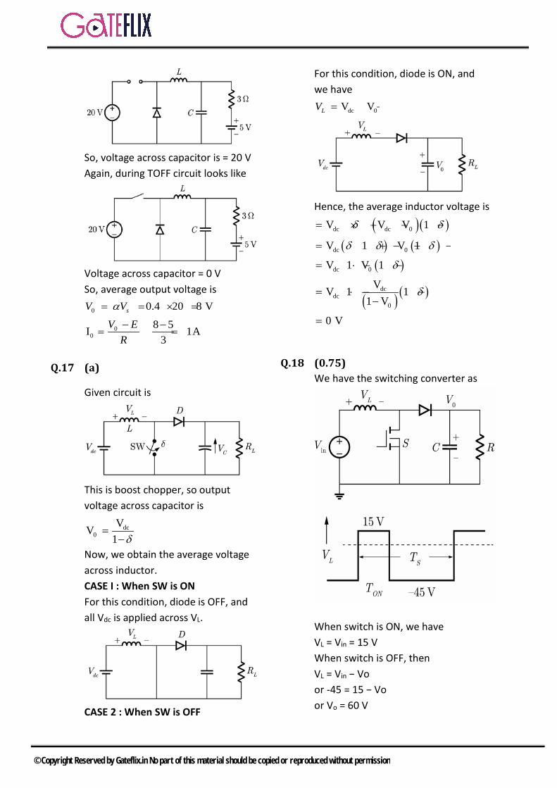
So, voltage across capacitor is = 20 V Again, during TOFF circuit looks like
Voltage across capacitor = 0 V So, average output voltage is
0
00
0.4 20 8 V
8 5I 1A3
sV VV E
R
α= = × =
− −= = =
Q.17 (a)
Given circuit is
This is boost chopper, so output voltage across capacitor is
dc0
VV1 δ
=−
Now, we obtain the average voltage across inductor. CASE I : When SW is ON For this condition, diode is OFF, and all Vdc is applied across VL.
CASE 2 : When SW is OFF
For this condition, diode is ON, and we have
dc 0V VLV = −
Hence, the average inductor voltage is
( )( )( ) ( )
( )
( ) ( )
dc dc 0
dc 0
dc 0
dcdc
0
V V V 1
V 1 V 1
V 1 V 1
VV 1 11 V
0 V
δ δ
δ δ δ
δ
δ
= × + − −
= + − − −
= ⋅ − −
= ⋅ − −−
=
Q.18 (0.75) We have the switching converter as
When switch is ON, we have VL = Vin = 15 V When switch is OFF, then VL = Vin − Vo or -45 = 15 − Vo or Vo = 60 V
© Copyright Reserved by Gateflix.in No part of this material should be copied or reproduced without permission
So, this is a step-up chopper, and therefore we have
so
VV1
15or 601
Hence, 0.75
α
αα
=−
=−=
Q.19 (2500)
33
12
1 0.65x10² 100 10
2.5
cL L Rf
Rx x
R k
α
−
−= =
− =
= Ω
Q.20 (0.4)
ON L g o
L o
g
g
o g
Sol:T Period: V = V V = 30 V _(1)
TOFF period: V = V = 20VBy solving both the equationsV 20 = 30
V = 50V
V = DV20 = D (50)
2D = 0.45
−
− −
−
=
Q.21 (60)
Load power, P0 = V0 I0 = 72W
0
0 dc dc
72I 2A36
D DV V 36 V1 D 1 D
= =
= × ⇒ = ×− −
0ON
IRipple voltage, V = . TC
∆
( )0
3 3
I D 2 0.6V = 0.06VC f 10 20 10−
×∆ = =
× ×
( )peak oV 0.06V V avg + 36.03V2 2∆
= + =
S peakPeak voltage across switch (V ) = 24 +36.03V = 60.03V Ans : 60.03
Q.22 (3.51)
( )
( ) ( ) ( )
( )
( ) ( )
dc0
0 0 0
0
0
0L
2
L L LRms avg
L ripple Rms
L(ripple rms)
L LRms avg
VOutput voltage, V1 D
3604001 D
D = 0.1P = V I4000 = 400 × II = 10A
I 10 10I avg = A1 D 1 0.1 0.9
I I 2 I ripple
ILI2 3
By neglecting ripple current, I = 0
I I
Rms
=−
=−
= =− −
= +
∆=
= =
( )Rms L Rms
10 A0.9
(ISW) = D I
100.1 3.513A0.9
Ans : 3.51
= × =
Q.23 (a) In Buck – Boost converter, output
voltage 0 dcDV V
1 D=
−D48
148 48
4848
48 3Where 32 .32 48 5
dc
dc
dc
dc
VD
D DV
DV
V V D
=−
− =
=+
= = =+
© Copyright Reserved by Gateflix.in No part of this material should be copied or reproduced without permission
48 270 ,72 48 52 3The duty ratio range =5 5
dcWhen V V D
D
= = =+
≤ ≤
Q.24 (40)
Q.25 (25)
s
1 2
0 s
(i) V 100 V(ii) Interleaved converters.(iii)Load resistance =1(iv) Switching frequency = 1 kHzCase I : When S ON, S OpenV V (As the average voltage across inductor is zero at steady state)Case II : W
=
Ω
→ →
=
2 1
0 s
0 s
00
hen S ON, S OpenV V (As the average voltage across inductor is zero steady state)Hence, V is always equal to V
100 100A1
Since the load current is equal divided in two inductive element. Henc
VIR
→ →
=
= = =
( ) ( )
( ) ( ) ( ) ( )
( ) ( )
( ) ( )
1 2
1 1 2 2
ON
1 1
2 2
e,50A
T 0.5Where, D = Duty ratio = 0.5T 1
Hence, 0.5 50 25A
0.5 50 25A
L avg L avg
S avg L avg S avg L avg
S avg L avg
S avg L avg
I I
I DI and I DI
I DI
I DI
= =
=
= =
= = × =
= = × =
Hence, the average value of switch (S1) current is 25 A.
© Copyright Reserved by Gateflix.in No part of this material should be copied or reproduced without permission
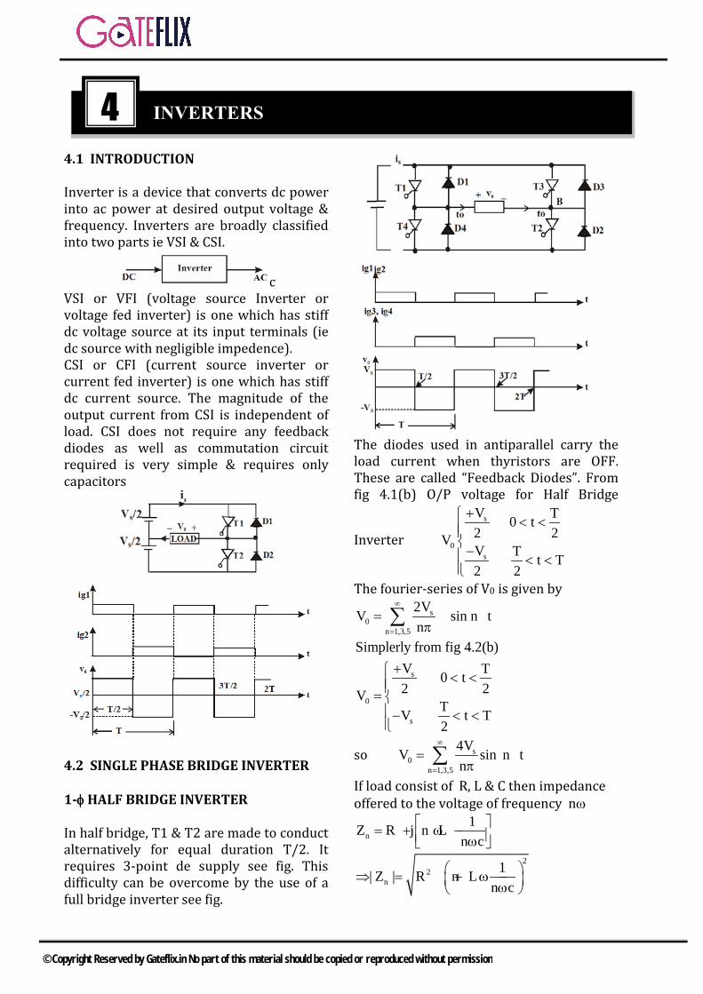
4.1 INTRODUCTION
Inverter is a device that converts dc power into ac power at desired output voltage & frequency. Inverters are broadly classified into two parts ie VSI & CSI.
c VSI or VFI (voltage source Inverter or voltage fed inverter) is one which has stiff dc voltage source at its input terminals (ie dc source with negligible impedence). CSI or CFI (current source inverter or current fed inverter) is one which has stiff dc current source. The magnitude of the output current from CSI is independent of load. CSI does not require any feedback diodes as well as commutation circuit required is very simple & requires only capacitors
4.2 SINGLE PHASE BRIDGE INVERTER
1-φ HALF BRIDGE INVERTER
In half bridge, T1 & T2 are made to conduct alternatively for equal duration T/2. It requires 3-point de supply see fig. This difficulty can be overcome by the use of a full bridge inverter see fig.
The diodes used in antiparallel carry the load current when thyristors are OFF. These are called “Feedback Diodes”. From fig 4.1(b) O/P voltage for Half Bridge
Inverter s
0s
V T 0 t2 2VV T t T2 2
+ < <− < <
The fourier-series of V0 is given by s
0n 1,3,5
2VV sin n tn
∞
=
= ωπ∑
Simplerly from fig 4.2(b)
s
0
s
V T 0 t2 2V
TV t T2
+ < <= − < <
so s0
n 1,3,5
4VV sin n tn
∞
=
= ωπ∑
If load consist of R, L & C then impedance offered to the voltage of frequency nω
n1Z R j n L
n c = + ω − ω
22
n1| Z | R n L
n c ⇒ = + ω − ω
4 INVERTERS
© Copyright Reserved by Gateflix.in No part of this material should be copied or reproduced without permission
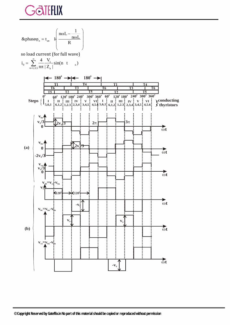
n an
1n Ln L&phase t 1
R
ω − ωϕ = −
so load current (for full wave) s
0 nn 1,3,5 n
V4i sin(n t )n | Z |
∞
=
= ω −ϕπ∑
ωt
ωt
ωt
ωt
ωt
ωt
00600 1200 1800 2400 3000 3600 600 1200 1800 2400 3000 3600
I5,6,1
II6,1,2
III1,2.3
IV2,3,4
V3,4,5
VI4,5.6
I5,6,1
II6,1,2
III1,2.3
IV2,3,4
V3,4,5
VI4,5.6
vbo
v /3S
02v /3S 2π 3π
2v /3S
-2v /3S
vbo
0
vcov /3S
0
v =v -vab ca ba
vS
1200 1200
-vS
vS vS
v =v -vbc ba ba
v =v -vca ba ba
-vS
Steps
(a)
(b)
conductingthyristors
© Copyright Reserved by Gateflix.in No part of this material should be copied or reproduced without permission
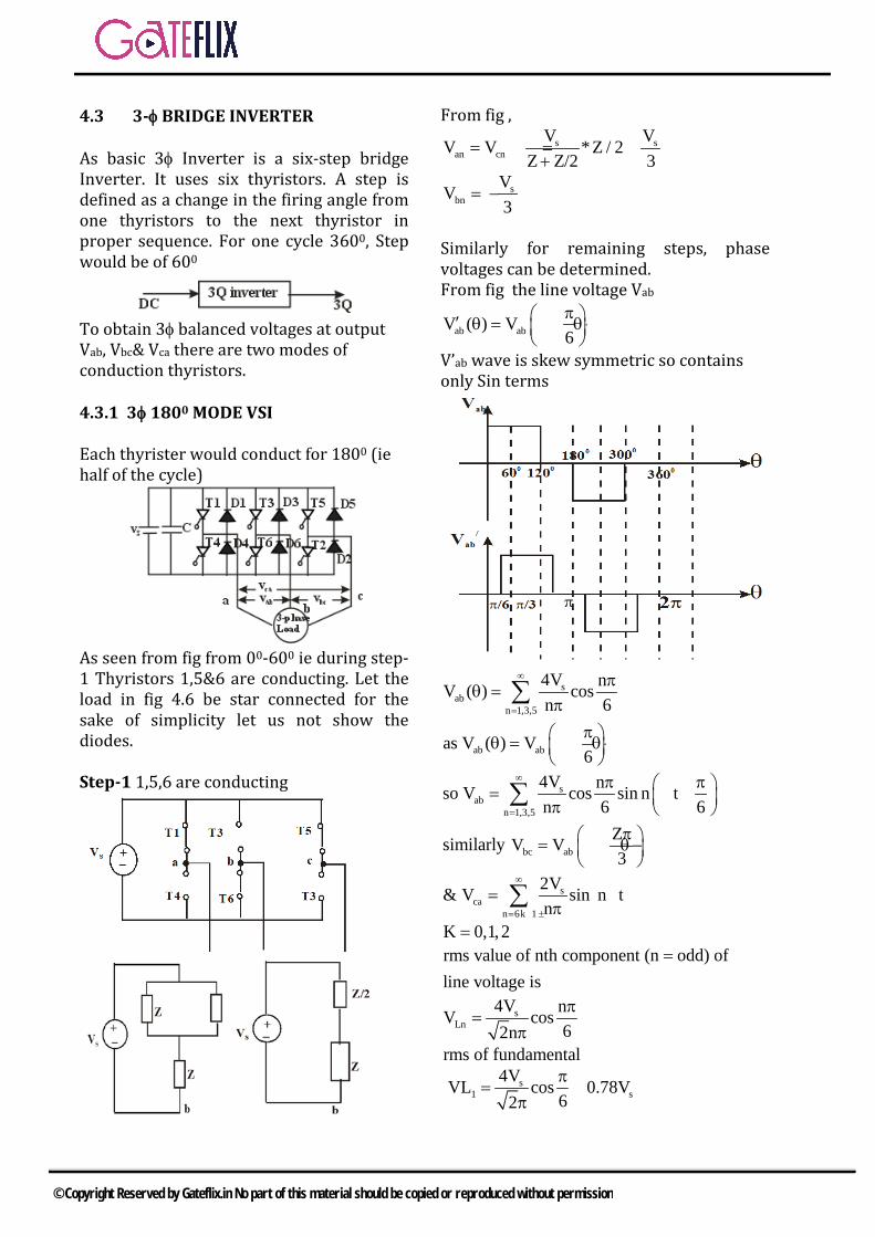
4.3 3-φ BRIDGE INVERTER
As basic 3φ Inverter is a six-step bridge Inverter. It uses six thyristors. A step is defined as a change in the firing angle from one thyristors to the next thyristor in proper sequence. For one cycle 3600, Step would be of 600
To obtain 3φ balanced voltages at output Vab, Vbc& Vca there are two modes of conduction thyristors.
4.3.1 3φ 1800 MODE VSI
Each thyrister would conduct for 1800 (ie half of the cycle)
As seen from fig from 00-600 ie during step-1 Thyristors 1,5&6 are conducting. Let the load in fig 4.6 be star connected for the sake of simplicity let us not show the diodes.
Step-1 1,5,6 are conducting
From fig , s s
an cnV VV V * Z / 2
Z Z/2 3= = =
+s
bnVV3
= −
Similarly for remaining steps, phase voltages can be determined. From fig the line voltage Vab
ab abV ( ) V6π ′ θ = θ−
V’ab wave is skew symmetric so contains only Sin terms
sab
n 1,3,5
4V nV ( ) cosn 6
∞
=
πθ =
π∑
ab abas V ( ) V6π θ = θ+
sab
n 1,3,5
4V nso V cos sin n tn 6 6
∞
=
π π = ω + π ∑
similarly bc abZV V3π = θ−
sca
n 6k 1
2V& V sin n tn
∞
= ±
= ωπ∑
K 0,1,2=
rms value of nth component (n odd) of line voltage is
=
sLn
4V nV cos62nπ
=π
rms of fundamental s
1 s4VVL cos 0.78V
62π
= =π
© Copyright Reserved by Gateflix.in No part of this material should be copied or reproduced without permission
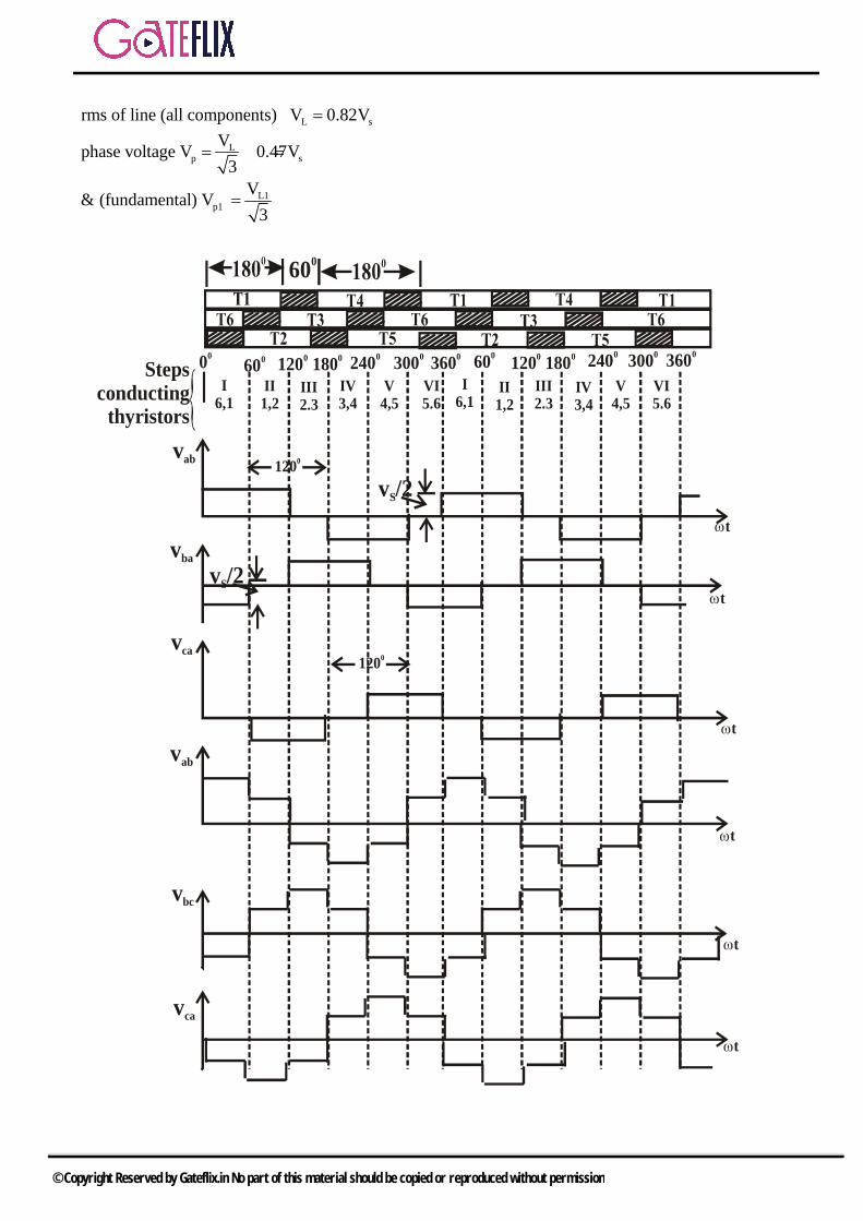
L srms of line (all components) V 0.82V=
Lp s
Vphase voltage V 0.47V3
= =
L1p1
V& (fundamental) V3
=
00600 1200 1800 2400 3000 3600 600 1200 1800 2400 3000 3600
I6,1
II1,2
III2.3
IV3,4
V4,5
VI5.6
I6,1
II1,2
III2.3
IV3,4
V4,5
VI5.6
Stepsconducting
thyristors
600
vab
vba
vca
vab
vbc
vca
1200
v /2S
v /2S
1200
ωt
ωt
ωt
ωt
ωt
ωt
© Copyright Reserved by Gateflix.in No part of this material should be copied or reproduced without permission
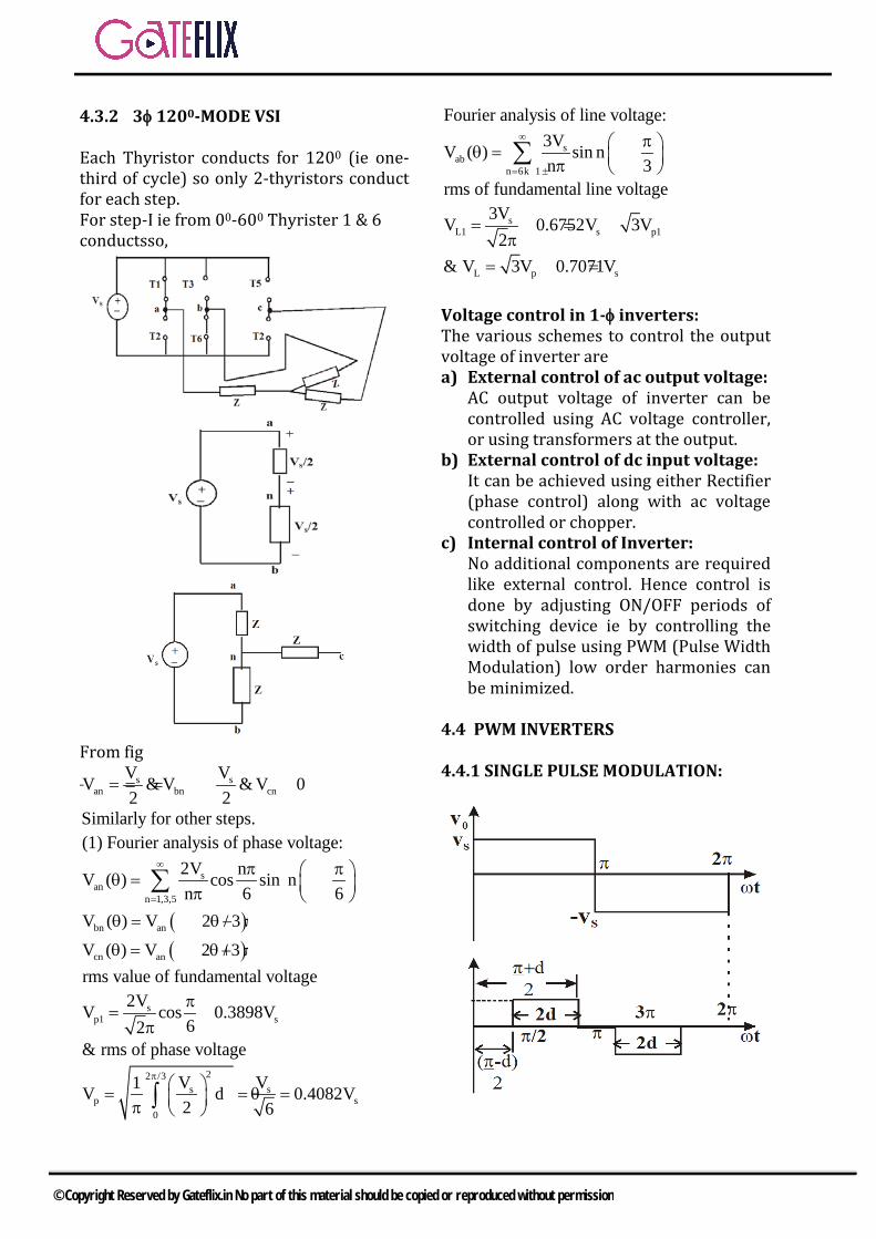
4.3.2 3φ 1200-MODE VSI
Each Thyristor conducts for 1200 (ie one-third of cycle) so only 2-thyristors conduct for each step. For step-I ie from 00-600 Thyrister 1 & 6 conductsso,
From fig s s
an bn cnV VV & V & V 02 2
= = − =
Similarly for other steps. (1) Fourier analysis of phase voltage:
san
n 1,3,5
2V nV ( ) cos sin nn 6 6
∞
=
π π θ = θ+ π ∑
( )bn anV ( ) V 2 / 3θ = θ− π
( )cn anV ( ) V 2 / 3θ = θ+ π
rms value of fundamental voltage s
p1 s2VV cos 0.3898V
62π
= =π
& rms of phase voltage 22 /3
s sp s
0
V V1V d 0.4082V2 6
π = θ = = π ∫
Fourier analysis of line voltage:
sab
n 6k 1
3VV ( ) sin nn 3
∞
= ±
π θ = θ+ π ∑
rms of fundamental line voltages
L1 s p13VV 0.6752V 3V
2= = =
π
L p s& V 3V 0.7071V= =
Voltage control in 1-φ inverters: The various schemes to control the output voltage of inverter are a) External control of ac output voltage:
AC output voltage of inverter can becontrolled using AC voltage controller,or using transformers at the output.
b) External control of dc input voltage:It can be achieved using either Rectifier(phase control) along with ac voltagecontrolled or chopper.
c) Internal control of Inverter:No additional components are requiredlike external control. Hence control isdone by adjusting ON/OFF periods ofswitching device ie by controlling thewidth of pulse using PWM (Pulse WidthModulation) low order harmonies canbe minimized.
4.4 PWM INVERTERS
4.4.1 SINGLE PULSE MODULATION:
© Copyright Reserved by Gateflix.in No part of this material should be copied or reproduced without permission

Fig (a) shows O/P voltage of 1-φ inverter, the width of the pulses in each half cycle is π rud. If by proper switching of thyristers this pulse width is modulated to 2d located symmetrically. Fourier analysis of modulated wave shows that
s0
n 1,3,5
4V nV sin sin n tn 2
∞
=
π= ω
π∑
fundamental component V01 = s4Vπ
sin d
where nth harmonic
Von = s4Vnπ
sin nd
rms value of O/P voltage 2
or s s2d 2dV V V= =π π
4.4.2 MULTIPLE-PULSE MODULATION
In MPM, there are several equilistant pulses perhalf cycle.
Fig , where two pulses per last cycle, located symmetrically. Fourier analysis of 2-pulse modulation gives
s0
n 1,3,5
8V ndV sin n sin sin n tn 2
∞
=
= γ ωπ∑
nth harmonic content s
on8V ndV sin n sinn 2
= γπ
from fig 4.14(b) it can be seen 2d d
N Nπ−
γ = +
where 2d→total PW N→no of pulses per half cycle rms value of O/P voltage
or s2dV V=π
4.4.3 SINUSOIDAL-PHASE MODULATION (SIN M) In sin M technique there are several pulses per half cycle like MPM but each pulse width is not equal as that in MPM, in sin M, the pulse width is a sinusoidal function of the angular position of the pulse see fig 4.15
d d
d d
γ+ 2
d
γ
( -d)γ 2
π/2 π-VS
3 /2π ωt
v0
vS
© Copyright Reserved by Gateflix.in No part of this material should be copied or reproduced without permission

& (b) (d) for realizing sin M, a high frequency triangular carrier wave Vc is compared with a sinusoidal reference wave Vr of designed frequency. If triangular wave φ zero coincide with sinusoid no. of
pulses/half cycle cfN 12f
= −
Modulation index- r
c
VMIV
=
MI Controls the magnitude of the output voltage.
© Copyright Reserved by Gateflix.in No part of this material should be copied or reproduced without permission
Q.1 A single-phase full bridge voltage source inverter feeds a purely induction load, as shown in figure. When T1, T2, T3, T4 are power transistors and D1, D2, D3, D4 are feedback diodes. The inverter is operated in square wave mode with a frequency of 50 Hz. If the average load current is zero, what is the time duration of conduction of each feedback diode in a cycle?
a) 5 msec b) 10msecc) 20 msec d) 2.5 msec
[GATE-2001]
Q.2 Figure (a) shows an inverter circuit with a dc source voltageVs . The semiconductor switches of the inverter are operated in such a manner that the pole voltage V10 and V20 are as shown in figure (b) what is the rms value of the pole-to-pole voltage V12
a) sVπ2
φ b) sVπφ
c) sV2πφ d) sV
π [GATE-2002]
Statement for common data 3 and 4 An inverter has a periodic output voltage with the output waveform as shown in figure.
Q.3 When the conduction angle α =120° , the rms fundamental component of the output voltage is a) 0.78 V b) 1.10 Vc) 0.90 V d) 1.27 V
[GATE-2003]
Q.4 With reference to the output waveform given in figure, the output of the converter will be free from 5th harmonic when a ) °α 72= b) °α 36=c) °α 150= d) °α 120=
[GATE-2003]
Q.5 The output voltage waveform of a three-phase square-wave inverter contains a) only even harmonicsb) both odd and even harmonics
GATE QUESTIONS
© Copyright Reserved by Gateflix.in No part of this material should be copied or reproduced without permission

c) only odd harmonicsd) only triple harmonics
[GATE-2005]
Q.6 A single-phase inverter is operated in PWM mode generating a single-pulse of width 2d in the centre of each half cycle as shown in figure. It is found that the output voltage is free from 5th harmonic for pulse width144°. What will be percentage of 3rd harmonic present in the output voltage ( )03 01maxV / V ?
a) 0.0 % b) 19.6 %c) 31.7 % d) 53.9 %
[GATE-2006]
Q.7 A single-phase voltages source inverter is controlled in a single pulse-width modulated mode with a pulse width of 150° in each half cycle. Total harmonic distortion is defined as
2 2rms 1
1
V VTHD 100
V−
= ×
When V1 is the rms value of the fundamental component of the output voltage. The THD of output ac voltage waveform is a) 65.65% b) 48.42%c) 31.83% d) 30.49%
[GATE-2007]
Q.8 A 3-phase voltage source Inverter is operated in 180° conduction mode. Which one of the following statements is true? a) Both pole-voltage and line-
voltage will have 3rd harmoniccomponents
b) Pole-voltage will have 3rdharmonic component but line-
voltage will be free from 3rd harmonic
c) Line-voltage will have 3rdharmonic component but pole-voltage will be freefrom 3rdharmonic
d) Both pole-voltage and line-voltage will be free 3rd harmoniccomponents.
[GATE-2008]
Q.9 A single phase voltage source inverter is feeding a purely inductive load as shown in the figure
The inverter is operated at 50 Hz in 180° square wave mode. Assume that the load current does not have any dc component. The peak value of the inductor current i0 will be a) 6.37 A b) 10 Ac) 20 A d) 40 A
[GATE-2008]
Q.10 The current source Inverter shown in figure is operated by alternately turning on thyristor pairs T1, T2 and T3, T4. If the load is purely resistive, the theoretical maximum output frequency obtainable will be
a) 125 kHz b) 250 kHzc) 500 kHz d) 50 kHz
[GATE-2009]
Q.11 A three-phase current source inverter used for the speed control
© Copyright Reserved by Gateflix.in No part of this material should be copied or reproduced without permission
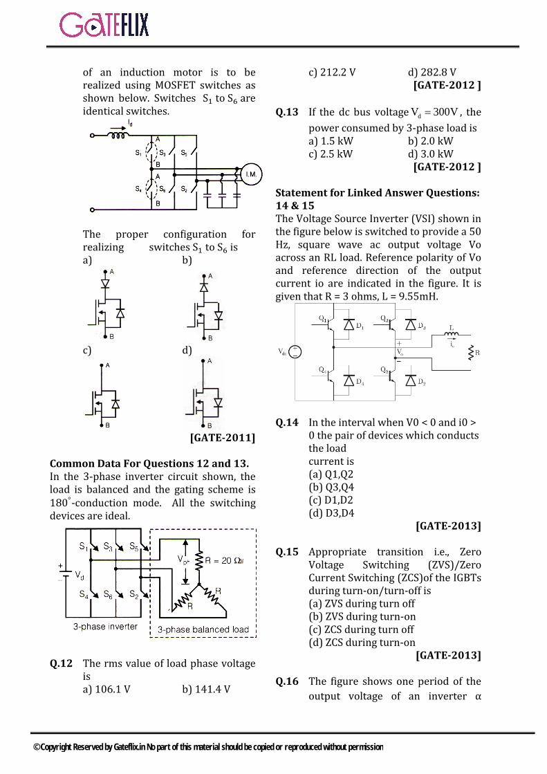
of an induction motor is to be realized using MOSFET switches as shown below. Switches S1 to S6 are identical switches.
The proper configuration for realizing switches S1 to S6 is a) b)
c) d)
[GATE-2011]
Common Data For Questions 12 and 13. In the 3-phase inverter circuit shown, the load is balanced and the gating scheme is 180°-conduction mode. All the switching devices are ideal.
Q.12 The rms value of load phase voltage is a) 106.1 V b) 141.4 V
c) 212.2 V d) 282.8 V [GATE-2012 ]
Q.13 If the dc bus voltage dV 300V= , the power consumed by 3-phase load is a) 1.5 kW b) 2.0 kWc) 2.5 kW d) 3.0 kW
[GATE-2012 ]
Statement for Linked Answer Questions: 14 & 15 The Voltage Source Inverter (VSI) shown in the figure below is switched to provide a 50 Hz, square wave ac output voltage Vo across an RL load. Reference polarity of Vo and reference direction of the output current io are indicated in the figure. It is given that R = 3 ohms, L = 9.55mH.
Q.14 In the interval when V0 < 0 and i0 > 0 the pair of devices which conducts the load current is (a) Q1,Q2 (b) Q3,Q4 (c) D1,D2 (d) D3,D4
[GATE-2013]
Q.15 Appropriate transition i.e., Zero Voltage Switching (ZVS)/Zero Current Switching (ZCS)of the IGBTs during turn-on/turn-off is (a) ZVS during turn off (b) ZVS during turn-on (c) ZCS during turn off (d) ZCS during turn-on
[GATE-2013]
Q.16 The figure shows one period of the output voltage of an inverter α
© Copyright Reserved by Gateflix.in No part of this material should be copied or reproduced without permission
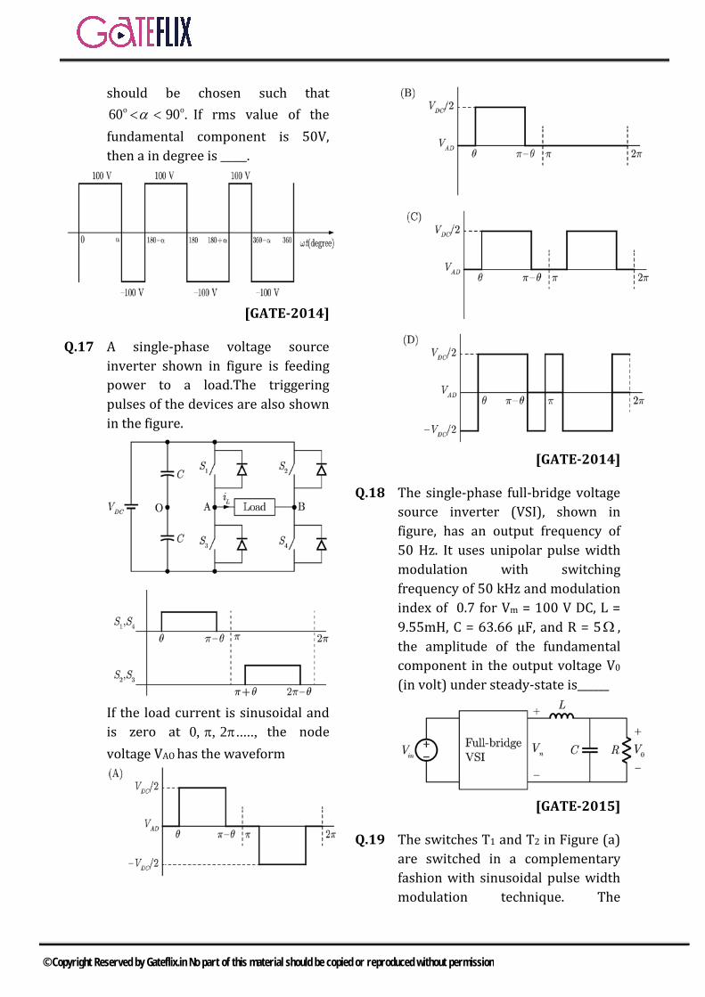
should be chosen such that o o60 90 .α< < If rms value of the
fundamental component is 50V, then a in degree is _____.
[GATE-2014]
Q.17 A single-phase voltage source inverter shown in figure is feeding power to a load.The triggering pulses of the devices are also shown in the figure.
If the load current is sinusoidal and is zero at 0, , 2 .....,π π the node voltage VAO has the waveform
[GATE-2014]
Q.18 The single-phase full-bridge voltage source inverter (VSI), shown in figure, has an output frequency of 50 Hz. It uses unipolar pulse width modulation with switching frequency of 50 kHz and modulation index of 0.7 for Vm = 100 V DC, L = 9.55mH, C = 63.66 μF, and R = 5Ω , the amplitude of the fundamental component in the output voltage V0 (in volt) under steady-state is______
[GATE-2015]
Q.19 The switches T1 and T2 in Figure (a) are switched in a complementary fashion with sinusoidal pulse width modulation technique. The
© Copyright Reserved by Gateflix.in No part of this material should be copied or reproduced without permission
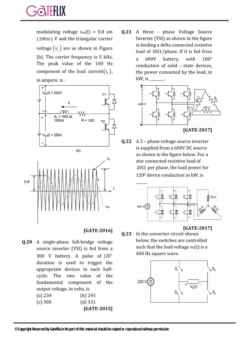
modulating voltage νm(t) = 0.8 sin ( )200 tπ V and the triangular carrier
voltage ( )cv are as shown in Figure
(b). The carrier frequency is 5 kHz. The peak value of the 100 Hz component of the load current ( )Li ,
in ampere, is .
[GATE-2016]
Q.20 A single-phase full-bridge voltage
source inverter (VSI) is fed from a 300 V battery. A pulse of o120duration is used to trigger the appropriate devices in each half-cycle. The rms value of the fundamental component of the output voltage, in volts, is (a) 234 (b) 245 (c) 300 (d) 331
[GATE-2015]
Q.21 A three - phase Voltage Source Inverter (VSI) as shown in the figure is feeding a delta connected resistive load of 30Ω /phase. If it is fed from a 600V battery, with 180° conduction of solid - state devices, the power consumed by the load, in kW, is ________.
[GATE-2017]
Q.22 A 3 – phase voltage source inverter
is supplied from a 600V DC source as shown in the figure below. For a star connected resistive load of 20Ω per phase, the load power for 1200 device conduction in kW, is ______
[GATE-2017]
Q.23 In the converter circuit shown below, the switches are controlled such that the load voltage ν0(t) is a 400 Hz square wave.
© Copyright Reserved by Gateflix.in No part of this material should be copied or reproduced without permission

The RMS value of the fundamental component of νo(t) in volts is _____.
[GATE-2017]
Q.24 A three – phase voltage source inverter with ideal devices operating in 1800 conduction mode is feeding a balanced star – connected resistive load. The DC voltage input is Vdc. The peak of the fundamental component of the phase voltage is
(a) dcVπ
(b) dc2Vπ
(c) dc3Vπ
(d) dc4Vπ
[GATE-2017]
Q.25 The figure below shows a half – bridge voltage source inverter supplying an RL –load with
0.3R = 40 and L = H. Ω π
The desired fundamental frequency of the load voltage is 50 Hz. The switch control signals of the converter are generated using sinusoidal pulse width modulation with modulation index. M = 0.6. At 50 Hz, the RL – load draws an active power of1.44 kW. The value of DC source voltage VDC. In volts is
(a) 300 2 (b) 500
(c) 500 2 (d) 1000 2 s [GATE-2017]
1 2 3 4 5 6 7 8 9 10 11 12 13 (a) (b) (a) (a) (c) (b) (c) (d) (b) (b) (a) (b) (d) 14 15 16 17 18 19 20 21 22 23 24 25 (d) (d) 77.15 (d) 49.5 10 (a) 24 9 198.06 (b) (c)
ANSWER KEY:
© Copyright Reserved by Gateflix.in No part of this material should be copied or reproduced without permission
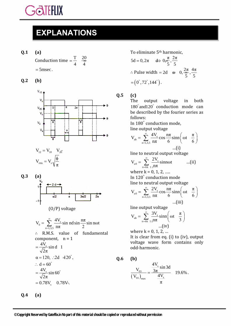
Q.1 (a)
Conduction time T 204 4
= =
5msec= .
Q.2 (b)
12 10 20V V V= −
rms sV Vπφ
=
Q.3 (a)
(O/P) voltage
s0
n 1,3,5
4V nπV sin ndsin sin nωtnπ 2
∞
=
= ∑∴ R.M.S. value of fundamental component, n = 1
s4V sin d 12π
= ×
°α 120, 2d 120 ,= ∴ =°d 60∴ =
°s4V sin 602π
=
s0.78V 0.78V= = .
Q.4 (a)
To eliminate 5th harmonic, π 2π5d 0, 2π d 0, ,5 5
= ⇒ =
∴ Pulse width 2π 4π2d α 0, ,5 5
= = =
( )° ° °0 ,72 ,144= .
Q.5 (c) The output voltage in both
° °180 and120 conduction mode can be described by the fourier series as follows: In 180° conduction mode, line output voltage
sab
n 1,3,5
4V nπ πV cos sinn ωtnπ 6 6
∞
=
= +
∑
…(i) line to neutral output voltage
sa0
n 6k 1
2VV sinnωtnπ
∞
= ±
= ∑ …(ii)
where k = 0, 1, 2, ….. In 120° conduction mode line to neutral output voltage
sa0
n 1,3,5
2V nπ πV cos sinn ωtnπ 6 6
∞
=
= +
∑
…(iii) line output voltage
sab
n 6k 1
3V πV sinn ωtnπ 3
∞
= ±
= +
∑…(iv)
where k = 0, 1, 2, … It is clear from eq. (i) to (iv), output voltage wave form contains only odd-harmonic.
Q.6 (b)
( )
s
03
s01 max
4V sin 3dV 3π 19.6%4VVπ
= = .
EXPLANATIONS
© Copyright Reserved by Gateflix.in No part of this material should be copied or reproduced without permission
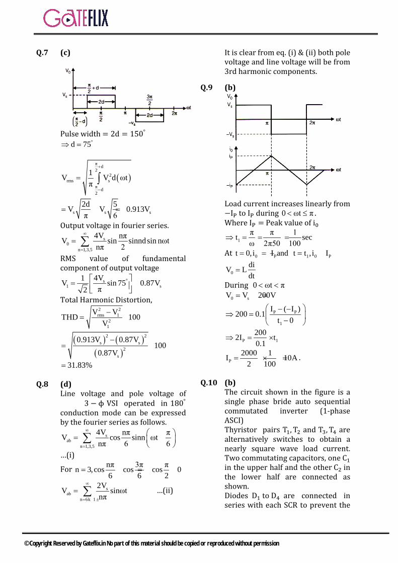
Q.7 (c)
Pulse width = 2d = 150° °d 75⇒ =
( )π d2
2rms s
π d2
1V V d ωtπ
+
−
= ∫
s s s2d 5V V 0.913Vπ 6
= = =
Output voltage in fourier series. s
0n 1,3,5
4V nπV sin sinndsin nωtnπ 2
∞
=
= ∑RMS value of fundamental component of output voltage
°s1 s
4V1V sin 75 0.87Vπ2
= = Total Harmonic Distortion,
2 2rms 1
21
V VTHD 100V−
= ×
( ) ( )( )
2 2s s
2s
0.913V 0.87V100
0.87V−
= ×
31.83%=
Q.8 (d) Line voltage and pole voltage of
3 − ϕ VSI operated in 180° conduction mode can be expressed by the fourier series as follows.
sab
n 1,3,5
4V nπ πV cos sinn ωtnπ 6 6
∞
=
= +
∑…(i)
For nπ 3π πn 3,cos cos cos 06 6 2
= = = =
sab
n 6k 1
2VV sinωtnπ
∞
= ±
= ∑ …(ii)
It is clear from eq. (i) & (ii) both pole voltage and line voltage will be from 3rd harmonic components.
Q.9 (b)
Load current increases linearly from −IP to IP during 0 ωt π< ≤ . Where IP = Peak value of i0
1π π 1t secω 2π50 100
⇒ = = =
At 0 Pt 0, i I and= = − 1 0 Pt t , i I= =
0diV Ldt
=
During 0 ωt π< < 0 sV V 200V= =
P P
1
I ( I )200 0.1t 0
− −⇒ = −
P 12002I t0.1
⇒ = ×
P2000 1I 10A
2 100= × = .
Q.10 (b) The circuit shown in the figure is a single phase bride auto sequential commutated inverter (1-phase ASCI) Thyristor pairs T1, T2 and T3, T4 are alternatively switches to obtain a nearly square wave load current. Two commutating capacitors, one C1 in the upper half and the other C2 in the lower half are connected as shown. Diodes D1 to D4 are connected in series with each SCR to prevent the
© Copyright Reserved by Gateflix.in No part of this material should be copied or reproduced without permission
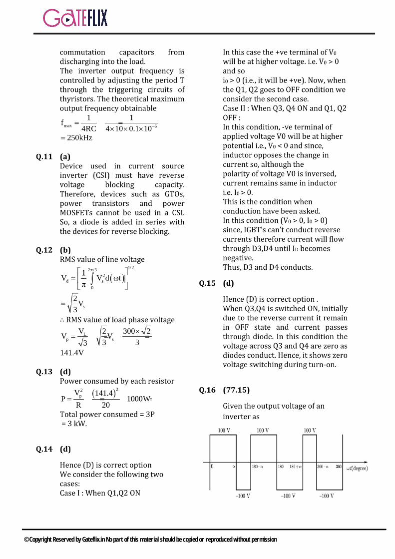
commutation capacitors from discharging into the load. The inverter output frequency is controlled by adjusting the period T through the triggering circuits of thyristors. The theoretical maximum output frequency obtainable
max 6
1 1f4RC 4 10 0.1 10−= =
× × ×250kHz=
Q.11 (a) Device used in current source inverter (CSI) must have reverse voltage blocking capacity. Therefore, devices such as GTOs, power transistors and power MOSFETs cannot be used in a CSI. So, a diode is added in series with the devices for reverse blocking.
Q.12 (b) RMS value of line voltage
( )1/22π/3
2d s
0
1V V d ωtπ
= ∫
s2V3
=
∴ RMS value of load phase voltage
Lp s
V 2 300 2V V3 33
×= = =
141.4V
Q.13 (d) Power consumed by each resistor
( )22pV 141.4
P 1000WR 20
= = =
Total power consumed = 3P = 3 kW.
Q.14 (d)
Hence (D) is correct option We consider the following two cases: Case I : When Q1,Q2 ON
In this case the +ve terminal of V0 will be at higher voltage. i.e. V0 > 0 and so i0 > 0 (i.e., it will be +ve). Now, when the Q1, Q2 goes to OFF condition we consider the second case. Case II : When Q3, Q4 ON and Q1, Q2 OFF : In this condition, -ve terminal of applied voltage V0 will be at higher potential i.e., V0 < 0 and since, inductor opposes the change in current so, although the polarity of voltage V0 is inversed, current remains same in inductor i.e. I0 > 0. This is the condition when conduction have been asked. In this condition (V0 > 0, I0 > 0) since, IGBT’s can’t conduct reverse currents therefore current will flow through D3,D4 until ID becomes negative. Thus, D3 and D4 conducts.
Q.15 (d)
Hence (D) is correct option . When Q3,Q4 is switched ON, initially due to the reverse current it remain in OFF state and current passes through diode. In this condition the voltage across Q3 and Q4 are zero as diodes conduct. Hence, it shows zero voltage switching during turn-on.
Q.16 (77.15)
Given the output voltage of an inverter as
© Copyright Reserved by Gateflix.in No part of this material should be copied or reproduced without permission
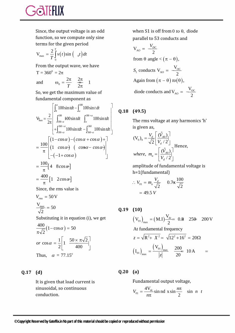
Since, the output voltage is an odd function, so we compute only sine terms for the given period
( ) ( )max 00
2V sinT
v t t dtT
= ω∫From the output wave, we have
0T = 360 = 2π
02 2and 1
2Tπ π
ω = = =π
So, we get the maximum value of fundamental component as
180
0180 180
max 180360 360
180 360
100sin 100sin2V 100sin 100sin
2100sin 100sin
tdt t dt
tdt tdt
tdt tdt
α
α
α
α α
α
α α
+
−
+
+ −
−
= + − π + −
∫ ∫∫ ∫∫ ∫
( ) ( )( ) ( )( )
[ ]
[ ]
( )
max
1100 1
1
100 4 8
400 1 2
Since, the rms value is50V
V 502
Substituting it in equation (i), we get400 1 cos 50
21 50 2cos 12 400
Th
rms
cos cos cos
cos cos cos
cos
cos
cos
V
or
α α α
α α α
α
α
α
α
α
− − + +
= − + − − π − − +
= −π
= −π
=
=
− =π
× π= −
ous, = 77.15α
Q.17 (d)
It is given that load current is sinusoidal, so continuous conduction.
when S1 is off from 0 to θ, diode parallel to 53 conducts and
AOV2DCV
= −
( )
( ) ( )
OC1 AO
OCAO
from angle < ,
Vconducts V2
Again from ,
Vdiode conducts and V2
S
to
θ π − θ
= −
π − θ θ
= −
Q.18 (49.5)
The rms voltage at any harmonics ‘h’ is given as,
00
0
ˆ( )(V )/ 22ˆ( ),/ 2
d Ah
d
Aa
d
V VV
Vwhere mV
=
=
Hence,
amplitude of fundamental voltage is h=1(fundamental)
011000.7x
2 249.5
da
VV m
V
∴ = =
=
Q.19 (10)
( ) ( )
( ) ( )
dc01 max
2 2 2 2
01 max01 max
VV M.I 0.8 250 200V2
At fundamental frequency
R 12 16 20
V 200I 10A20
z X
z
= = × =
= + = + = Ω
= = =
Q.20 (a)
Fundamental output voltage,
dc01
4V sin nd x sin sin2
nV n tn
π= × ω
π
© Copyright Reserved by Gateflix.in No part of this material should be copied or reproduced without permission
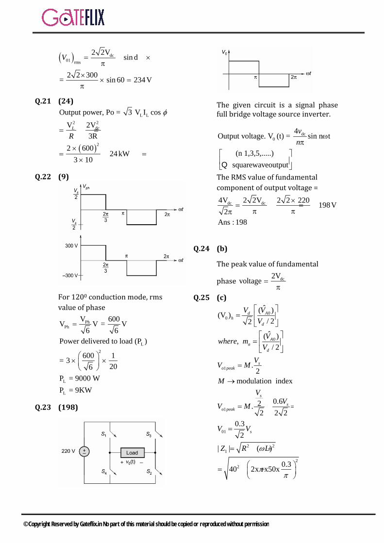
( ) dc01 rms
2 2V sin d
2 2 300= sin 60 234 V
V = ×π
×× =
π
Q.21 (24)
( )
L L22dc
2
Output power, Po = 3 V I cos2VV3R
2 60024kW
3 10
L
R
φ
= =
×= =
×
Q.22 (9)
For 1200 conduction mode, rms value of phase
PhPh
L2
L
L
V 600V V = V6 6
Power delivered to load (P )
600 1= 3206
P = 9000 WP = 9KW
=
× ×
Q.23 (198)
The given circuit is a signal phase full bridge voltage source inverter.
dc0
4Output voltage. V (t) = sin n tvn
ωπ
(n 1,3,5,.....)squarewaveoutput
Q
The RMS value of fundamental component of output voltage =
dc dc4V 2 2V 2 2 220 198V2
Ans : 198
×= = =
π ππ
Q.24 (b)
The peak value of fundamental
phase dc2Vvoltage =π
Q.25 (c)
00
0
1
1
ˆ( )(V )/ 22ˆ( ),/ 2
.2
modulation index
0.62.2 2 2
d Ah
d
Aa
d
so peak
s
so peak
V VV
Vwhere mV
VV M
MV
VV M
=
=
=
→
= =
01
2 21
22
0.32
| | ( )
0.340 2x x50x
sV V
Z R Lω
ππ
=
= +
= +
© Copyright Reserved by Gateflix.in No part of this material should be copied or reproduced without permission
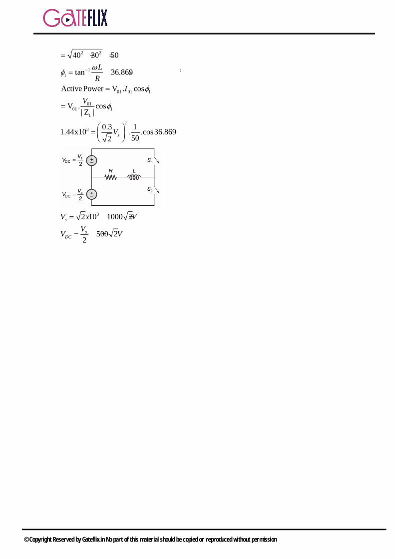
2 2
11
01 01 1
0101 1
12
3
40 30 50
tan 36.869
Active Power V . cos
V . cos| Z |
0.3 11.44x10 . .cos36.869502 s
LR
IV
V
ωφ
φ
φ
−
= + =
= = °
=
=
= °
32 10 1000 2
500 22
s
sDC
V x VVV V
= =
= =
© Copyright Reserved by Gateflix.in No part of this material should be copied or reproduced without permission
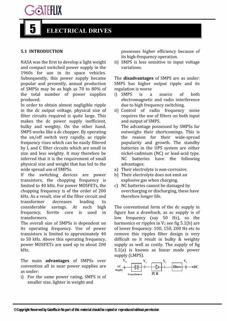
5.1 INTRODUCTION
NASA was the first to develop a light weight and compact switched power supply in the 1960s for use in its space vehicles. Subsequently, this power supply became popular and presently, annual production of SMPSs may be as high as 70 to 80% of the total number of power supplies produced. In order to obtain almost negligible ripple in the dc output voltage, physical size of filter circuits required is quite large. This makes the dc power supply inefficient, bulky and weighty. On the other hand, SMPS works like a dc chopper. By operating the on/off switch very rapidly, ac ripple frequency rises which can be easily filtered by L and C filter circuits which are small in size and less weighty. It may therefore be inferred that it is the requirement of small physical size and weight that has led to the wide spread use of SMPSs. If the switching devices are power transistors, the chopping frequency is limited to 40 kHz. For power MOSFETs, the chopping frequency is of the order of 200 kHz. As a result, size of the filter circuit and transformer decreases leading to considerable savings. At such high frequency, ferrite core is used in transformers. The overall size of SMPSs is dependent on its operating frequency. Use of power transistors is limited to approximately 40 to 50 kHz. Above this operating frequency, power MOSFETs are used up to about 200 kHz.
The main advantages of SMPSs over convention all in near power supplies are as under: i) For the same power rating, SMPS is of
smaller size, lighter in weight and
possesses higher efficiency because of its high-frequency operation.
ii) SMPS is less sensitive to input voltagevariations.
The disadvantages of SMPS are as under: SMPS has higher output ripple and its regulation is worse i) SMPS is a source of both
electromagnetic and radio interference due to high frequency switching.
ii) Control of radio frequency noiserequires the use of filters on both inputand output of SMPS.The advantage possessed by SMPSs faroutweighs their shortcomings. This isthe reason for their wide-spreadpopularity and growth. The standbybatteries in the UPS system are eithernickel-cadmium (NC) or lead-acid type.NC batteries have the followingadvantages:
a) Their electrolyte is non-corrosive.b) Their electrolyte does not emit an
explosive gas when charging.c) NC batteries cannot be damaged by
overcharging or discharging, these havetherefore longer life.
The conventional form of the dc supply in figure has a drawback, as ac supply is of low frequency (say 50 Hz), so the harmonics or ripples in V2 see fig 5.1(b) are of lower frequency. 100, 150, 200 Hz etc to remove this ripples filter design is very difficult so it result in bulky & weighty supply as well as costly. The supply of fig 5.1(a) is known as linear mode power supply (LMPS).
5 ELECTRICAL DRIVES
© Copyright Reserved by Gateflix.in No part of this material should be copied or reproduced without permission
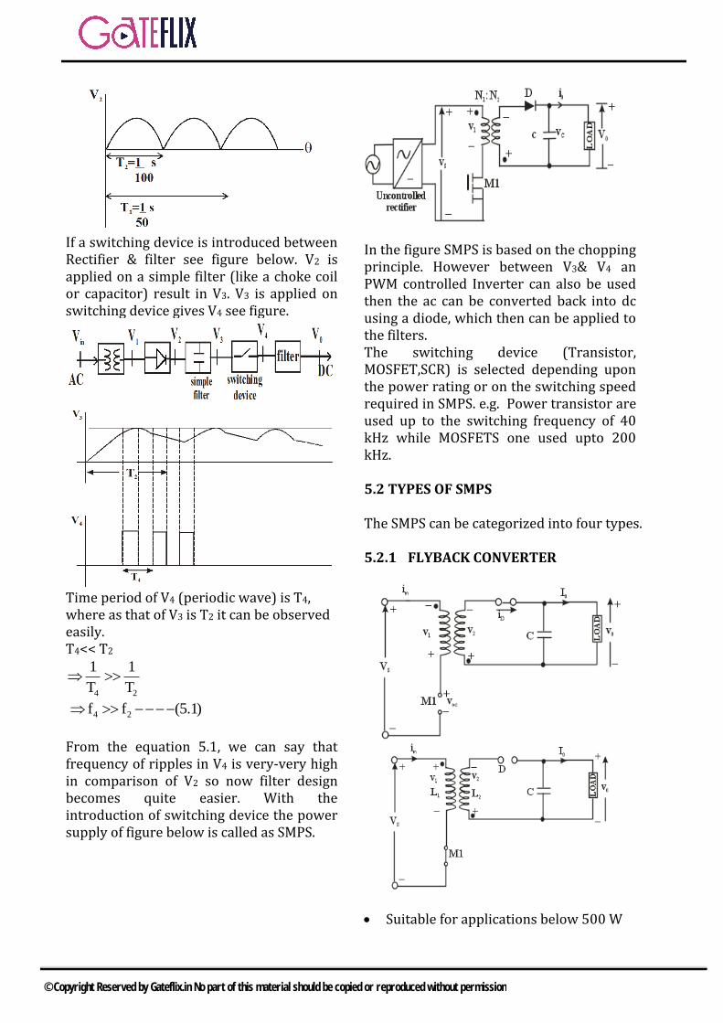
If a switching device is introduced between Rectifier & filter see figure below. V2 is applied on a simple filter (like a choke coil or capacitor) result in V3. V3 is applied on switching device gives V4 see figure.
Time period of V4 (periodic wave) is T4, where as that of V3 is T2 it can be observed easily. T4<< T2
4 2
1 1
T T
4 2f f (5.1)
From the equation 5.1, we can say that frequency of ripples in V4 is very-very high in comparison of V2 so now filter design becomes quite easier. With the introduction of switching device the power supply of figure below is called as SMPS.
In the figure SMPS is based on the chopping principle. However between V3& V4 an PWM controlled Inverter can also be used then the ac can be converted back into dc using a diode, which then can be applied to the filters. The switching device (Transistor, MOSFET,SCR) is selected depending upon the power rating or on the switching speed required in SMPS. e.g. Power transistor are used up to the switching frequency of 40 kHz while MOSFETS one used upto 200 kHz.
5.2 TYPES OF SMPS
The SMPS can be categorized into four types.
5.2.1 FLYBACK CONVERTER
Suitable for applications below 500 W
© Copyright Reserved by Gateflix.in No part of this material should be copied or reproduced without permission
It uses on uncontrolled rectifier (egdiode rectifier) a switching device (sayMOSFET M1) Isolating transformer.
When M1 is ON, magnetizing currentflow in primary of transformer [b’cozdiode is open hence secondary at no-load] so flux established from m0m1
so mi m0 vet t
so voltages are
induced with the polarity as shown withthis polarity of V2, Diode D is open V2 is
2 22 1 s
1 1
N NV V V
N N
When M1 is turned off, as im reduces tozero so flux also reduces from
mo m1m1 m0so ve
t t
Hence voltage induced will be oppositepolarity as that were, when M1 was ON,with this polarity of V2 Diode D is ON &as capacitor C is very large it givesoutput V0= almost constant. Thusenergy stored in transformer core isdelivered partly to load & portly tocharge the capacitor C.
During ON period of M1 say form t = 0 to
t = TON V1 = Vs, 22 s m0 m1
1
NV V ,I I
N
ID = 0 during OFF period of M1 say from t = TON to t = TON + TOFF
022 0 1
2 2
1 1
VVV V ,V
N N
N N
m mm m m0 D
2
1
i ii I I ,i
N a
N
m0m1D
IIsoi
a a
If resistances & leakage reactance ofTransformer be negligible & if itsmagnetizing inductance is L then
sm m0 ON
Vi (t) I 0 t T (5.2)
L
As current rises during 0<t<TON soenergy stored in transformer core so att = TON
sm ON m1 m0 ON
Vi (T ) I T T (5.3)
L
During M1 is off im decrease so energy isdelivered from core.
0 1m m1 ON ON
2
V N 0i (t) I t T T t T (5.4)
N L
So at
0 1m1 ON
2
V NI (t T )
N L
ON OFFatt T T T
0
0 1m m m1 ON
2
V V 0i T I I T T (5.5)
N L
from equation 5.3 substitute
0 1m1 ON
2
V N 1I T T
N L
so load voltage
s ON s0
ON
aV T aVV
T T 1
where ONT
T duty cycleso O/P
0 sV a V1
© Copyright Reserved by Gateflix.in No part of this material should be copied or reproduced without permission
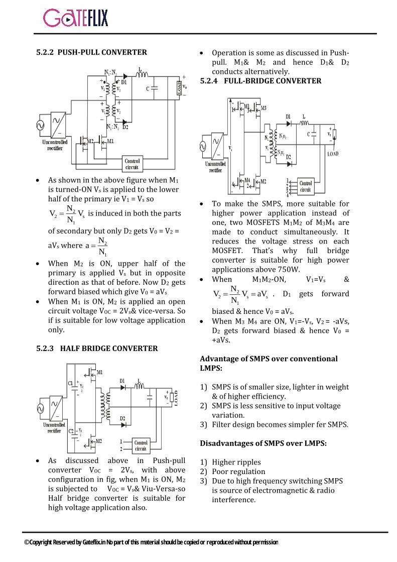
5.2.2 PUSH-PULL CONVERTER
As shown in the above figure when M1
is turned-ON Vs is applied to the lowerhalf of the primary ie V1 = Vs so
22 s
1
NV V
N is induced in both the parts
of secondary but only D2 gets V0 = V2 =
aVs where 2
1
Na
N
When M2 is ON, upper half of theprimary is applied Vs but in oppositedirection as that of before. Now D2 getsforward biased which give V0 = aVs
When M1 is ON, M2 is applied an opencircuit voltage VOC = 2Vs& vice-versa. Soif is suitable for low voltage applicationonly.
5.2.3 HALF BRIDGE CONVERTER
As discussed above in Push-pullconverter VOC = 2Vs, with aboveconfiguration in fig, when M1 is ON, M2
is subjected to VOC = Vs& Viu-Versa-soHalf bridge converter is suitable forhigh voltage application also.
Operation is some as discussed in Push-pull. M1& M2 and hence D1& D2
conducts alternatively.5.2.4 FULL-BRIDGE CONVERTER
To make the SMPS, more suitable forhigher power application instead ofone, two MOSFETS M1M2 of M3M4 aremade to conduct simultaneously. Itreduces the voltage stress on eachMOSFET. That’s why full bridgeconverter is suitable for high powerapplications above 750W.
When M1M2-ON, V1=Vs &
22 s s
1
NV V aV
N . D1 gets forward
biased & hence V0 = aVs. When M3 M4 are ON, V1=-Vs, V2 = -aVs,
D2 gets forward biased & hence V0 =+aVs.
Advantage of SMPS over conventional LMPS:
1) SMPS is of smaller size, lighter in weight& of higher efficiency.
2) SMPS is less sensitive to input voltagevariation.
3) Filter design becomes simpler fer SMPS.
Disadvantages of SMPS over LMPS:
1) Higher ripples2) Poor regulation3) Due to high frequency switching SMPS
is source of electromagnetic & radiointerference.
© Copyright Reserved by Gateflix.in No part of this material should be copied or reproduced without permission
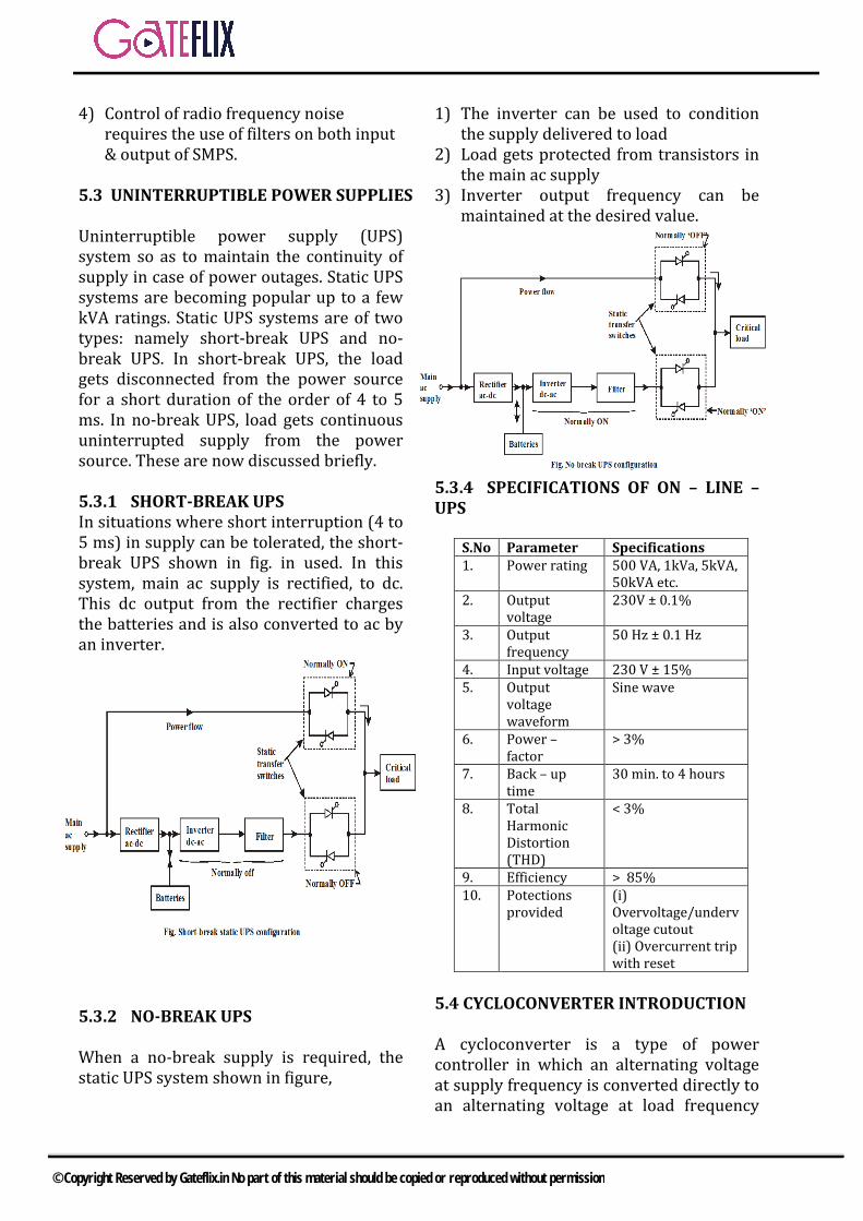
4) Control of radio frequency noiserequires the use of filters on both input& output of SMPS.
5.3 UNINTERRUPTIBLE POWER SUPPLIES
Uninterruptible power supply (UPS) system so as to maintain the continuity of supply in case of power outages. Static UPS systems are becoming popular up to a few kVA ratings. Static UPS systems are of two types: namely short-break UPS and no-break UPS. In short-break UPS, the load gets disconnected from the power source for a short duration of the order of 4 to 5 ms. In no-break UPS, load gets continuous uninterrupted supply from the power source. These are now discussed briefly.
5.3.1 SHORT-BREAK UPS In situations where short interruption (4 to 5 ms) in supply can be tolerated, the short-break UPS shown in fig. in used. In this system, main ac supply is rectified, to dc. This dc output from the rectifier charges the batteries and is also converted to ac by an inverter.
5.3.2 NO-BREAK UPS
When a no-break supply is required, the static UPS system shown in figure,
1) The inverter can be used to conditionthe supply delivered to load
2) Load gets protected from transistors inthe main ac supply
3) Inverter output frequency can bemaintained at the desired value.
5.3.4 SPECIFICATIONS OF ON – LINE – UPS
S.No Parameter Specifications 1. Power rating 500 VA, 1kVa, 5kVA,
50kVA etc. 2. Output
voltage 230V ± 0.1%
3. Output frequency
50 Hz ± 0.1 Hz
4. Input voltage 230 V ± 15% 5. Output
voltage waveform
Sine wave
6. Power – factor
> 3%
7. Back – up time
30 min. to 4 hours
8. Total Harmonic Distortion (THD)
< 3%
9. Efficiency > 85% 10. Potections
provided (i) Overvoltage/undervoltage cutout (ii) Overcurrent trip with reset
5.4 CYCLOCONVERTER INTRODUCTION
A cycloconverter is a type of power controller in which an alternating voltage at supply frequency is converted directly to an alternating voltage at load frequency
© Copyright Reserved by Gateflix.in No part of this material should be copied or reproduced without permission
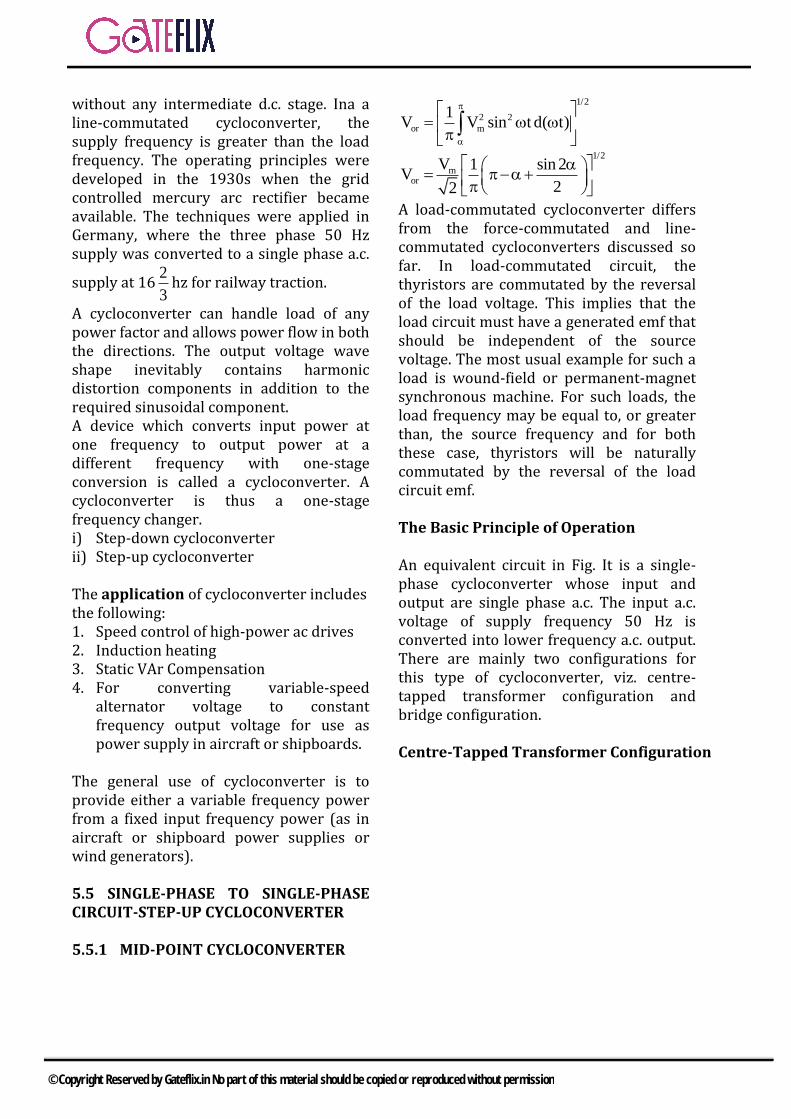
without any intermediate d.c. stage. Ina a line-commutated cycloconverter, the supply frequency is greater than the load frequency. The operating principles were developed in the 1930s when the grid controlled mercury arc rectifier became available. The techniques were applied in Germany, where the three phase 50 Hz supply was converted to a single phase a.c.
supply at 162
3hz for railway traction.
A cycloconverter can handle load of any power factor and allows power flow in both the directions. The output voltage wave shape inevitably contains harmonic distortion components in addition to the required sinusoidal component. A device which converts input power at one frequency to output power at a different frequency with one-stage conversion is called a cycloconverter. A cycloconverter is thus a one-stage frequency changer. i) Step-down cycloconverterii) Step-up cycloconverter
The application of cycloconverter includes the following: 1. Speed control of high-power ac drives2. Induction heating3. Static VAr Compensation4. For converting variable-speed
alternator voltage to constantfrequency output voltage for use aspower supply in aircraft or shipboards.
The general use of cycloconverter is to provide either a variable frequency power from a fixed input frequency power (as in aircraft or shipboard power supplies or wind generators).
5.5 SINGLE-PHASE TO SINGLE-PHASE CIRCUIT-STEP-UP CYCLOCONVERTER
5.5.1 MID-POINT CYCLOCONVERTER
1/2
2 2
or m
1V V sin t d( t)
1/2
mor
V 1 sin 2V
22
A load-commutated cycloconverter differs from the force-commutated and line-commutated cycloconverters discussed so far. In load-commutated circuit, the thyristors are commutated by the reversal of the load voltage. This implies that the load circuit must have a generated emf that should be independent of the source voltage. The most usual example for such a load is wound-field or permanent-magnet synchronous machine. For such loads, the load frequency may be equal to, or greater than, the source frequency and for both these case, thyristors will be naturally commutated by the reversal of the load circuit emf.
The Basic Principle of Operation
An equivalent circuit in Fig. It is a single-phase cycloconverter whose input and output are single phase a.c. The input a.c. voltage of supply frequency 50 Hz is converted into lower frequency a.c. output. There are mainly two configurations for this type of cycloconverter, viz. centre-tapped transformer configuration and bridge configuration.
Centre-Tapped Transformer Configuration
© Copyright Reserved by Gateflix.in No part of this material should be copied or reproduced without permission
Power circuit of a single-phase to single-phase cycloconverter employing a centre-tapped transformer. There are four thyristors, namely, P1, N1, P2, and N2. Out of the four SCRs P1 and P2 are responsible .
Example A single-phase bridge-type cycloconverter has input voltage of 230 V, 50 Hz and load of R = 10 Ω. Output frequency is one-third of input frequency. For a firing angle delay of 30o, calculate (a) rms value of output voltage (b) rms current of each converter (c) rms current of each thyristor and (d) input power factor.
Solution a) Here Vs = 230 V, Vm =
2 230V,R 10 , o30 .6
From
equation, we get
1/2o
or
2 230 1 sin 60V
6 22
226.66V
Rms value of load current,
oror
V 226.66I 22.67A
R 10
b) For an output frequency of fo, each
converter conducts foro
1
2f radians,
with a periodicity of 2π radians.
orp
IRms valueof current for each converter I
2
22.6716.03A
2
c) Each thyristors handles rms current forπ radians with a periodicity of 2π rad.
p orI I
Rms valueof current for each thyristor22
22.6711.335A
2
d) Rms source current, Is = Ior = 22.67 AInput VA = 230 × 22.67 VA, Load power= 22.672 × 10
222.67 10Input pf 0.9856lag.
230 22.67
With R-L load
© Copyright Reserved by Gateflix.in No part of this material should be copied or reproduced without permission
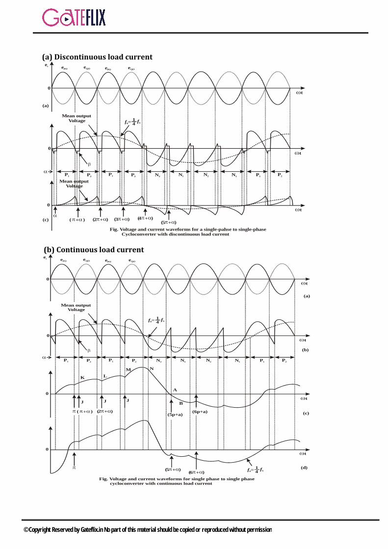
(a) Discontinuous load current
t
es
0
ePOeQO ePO
eQO
(a)
Mean output Voltage f0=
14
fS
0
Mean output Voltage
P1 P2N1N2
P1 P2N2 N1 P1
P2
t
t0
(c) ( )+ ( )+2 ( )+3 ( )+( )+
45
Fig. Voltage and current waveforms for a single-pahse to single-phase Cycloconverter with discontinuous load current
(b) Continuous load current
t
es
0
ePOeQO ePO
eQO
(a)
Mean output Voltage
f0=14
fS
0
P1 P2 N1N2P1 P2
N2 N1 P1P2
t
0
0
t
t
( )+5( )+6
f0=14
fS
(b)
(c)
(d)
K L
M N
A
B
( )+ ( )+2
J J J
(5p+a)(6p+a)
Fig. Voltage and current waveforms for single phase to single phase cycloconverter with continuous load current
© Copyright Reserved by Gateflix.in No part of this material should be copied or reproduced without permission
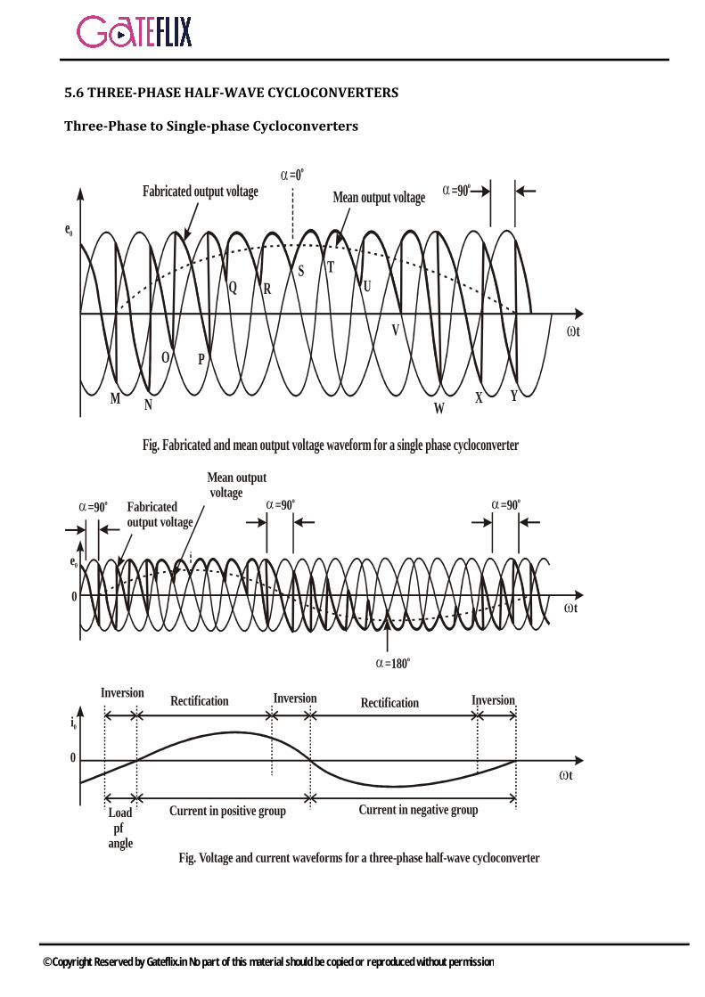
5.6 THREE-PHASE HALF-WAVE CYCLOCONVERTERS
Three-Phase to Single-phase Cycloconverters
e0
M N
O P
Q RS T
U
V
X YW
Fabricated output voltage Mean output voltage
=0o
=90o
t
Fig. Fabricated and mean output voltage waveform for a single phase cycloconverter
Fabricated output voltage
Mean outputvoltage
=90o
t
=90o =90
o
=180o
0
e0
0
i0
InversionRectification Inversion Rectification Inversion
Load pfangle
Current in positive group Current in negative group
t
Fig. Voltage and current waveforms for a three-phase half-wave cycloconverter
© Copyright Reserved by Gateflix.in No part of this material should be copied or reproduced without permission
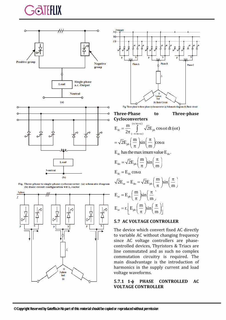
Three-Phase to Three-phase Cycloconverters
( /m )
dc ph
( /m )
mE 2E cos t dt ( t)
2
ph
m2E sin cos
m
dc doE has themaximumvalueE .
do ph
mE 2E sin
m
dc doE E cos
or do ph
m2E E 2E sin
m
or ph
mE E sin
m
or ph
mE r. E sin
m
5.7 AC VOLTAGE CONTROLLER
The device which convert fixed AC directly to variable AC without changing frequency since AC voltage controllers are phase-controlled devices, Thyristors & Triacs are line commutated and as such no complex commutation circuitry is required. The main disadvantage is the introduction of harmonics in the supply current and load voltage waveforms.
5.7.1 1- PHASE CONTROLLED AC VOLTAGE CONTROLLER
© Copyright Reserved by Gateflix.in No part of this material should be copied or reproduced without permission
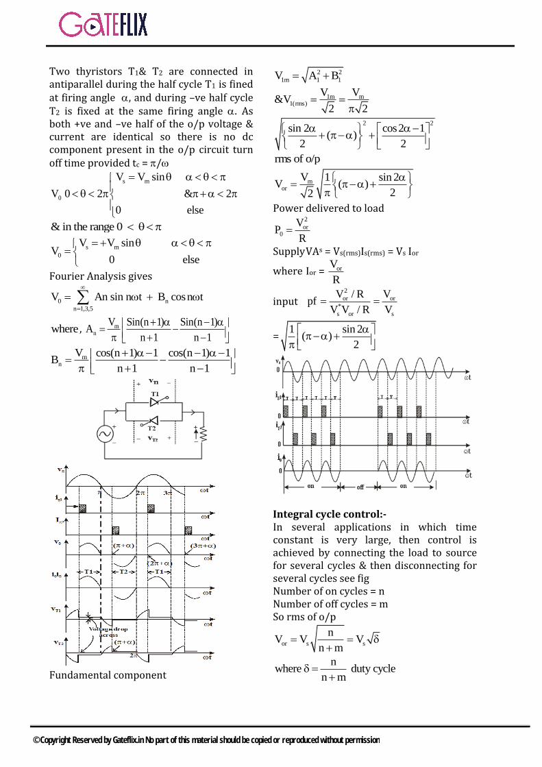
Two thyristors T1& T2 are connected in antiparallel during the half cycle T1 is fined at firing angle , and during –ve half cycle T2 is fixed at the same firing angle . As both +ve and –ve half of the o/p voltage & current are identical so there is no dc component present in the o/p circuit turn off time provided tc = /
0V
s mV V sin
0 2 & 2
0 else
& in the range 0
s m
0
V V sinV
0 else
Fourier Analysis gives
0 n
n 1,3,5
V An sin n t B cosn t
where , mn
V Sin(n 1) Sin(n 1)A
n 1 n 1
mn
V cos(n 1) 1 cos(n 1) 1B
n 1 n 1
Fundamental component
2 2
1m 1 1V A B
1m m1(rms)
V V&V
2 2
2 2sin 2 cos2 1
( )2 2
rms of o/p
mor
V 1 sin 2V ( )
22
Power delivered to load 2
or0
VP
R
Supply VAs = Vs(rms)Is(rms) = Vs Ior
where Ior = orV
R
input 2
or or
*
s or s
V / R Vpf
V V / R V
=1 sin 2
( )2
Integral cycle control:- In several applications in which time constant is very large, then control is achieved by connecting the load to source for several cycles & then disconnecting for several cycles see fig Number of on cycles = n Number of off cycles = m So rms of o/p
or s s
nV V V
n m
nwhere duty cycle
n m
© Copyright Reserved by Gateflix.in No part of this material should be copied or reproduced without permission

5.8 COMPARISON BETWEEN CYCLOCONVERTER AND D.C. LINK CONVERTER
A comparison between cycloconverter and d.c. link converter is given in a tabular form as follows:
Cycloconverter D.C. Link Converter 1) In a cycloconverter,a.c. power at one frequency is converted directly to a lower frequency in a single conversion stage.
1) d.c. link converter has two power controlles and the full output power is converted in two stages.
2) Cycloconverterfunctions by means of phase commutation and no auxiliary forced commutation circuits are necessary. This results in a more compact power circuit losses associated with forced commutation.
2) d.c. link converter, on the other hand, requires forced commutation for the inverter even though the rectifier operates on phase control principle.
3) Cycloconverter isinherently capable of power transfer in either direction between source and load. It can supply power to loads at any power factor and is also capable of regeneration at full power over the complete speed range, down to stand-still. This feature makes a cycloconverter preferable for large reversing and deceleration. This type of application occurs principally in the metal rolling industry.
3) This feature isslightly difficult and is involved to incorporate in a d.c. link converter.
4)Commutation failurecauses a short circuit of the a.c. supply. But if an individual thyristor fuse blows off, a complete shutdown is not necessary and the cycloconverter continues to function with somewhat distorted waveforms. A balanced load is
4) The d.c. linkconverter cannot provide this feature.
presented to the a.c. supply even with unbalanced output conditions. 5) Cycloconverterdelivers a high quality sinusoidal waveform at low output frequencies since it is often preferable for very low speed applications.
5) The d.c. linkconverter, on the other hand, generates a stepped waveform which may cause a nonuniform rotation of an a.c. motor at very low frequencies (<10 Hz). The distorted waveform also causes system instability at low frequencies.
6) For reasonablepower output and efficiency, the output frequency is limited to 1/3 input frequency.
6)The frequency canbe varied from zero to rated value. The upper frequency limit is divided by the device turn-off time.
7. Requires largernumber of thyristors and its control circuitry is more complex. This is not justified for small installations but it is economical for units 20 kVA and more.
(7) The d.c. link converter requires only 12 thyristors and control circuits are less involved.
8) Has very low powerfactor, particularly at reduced output voltages.
8) The d.c. linkconverter has high input power factor if diode rectifier is used . With phase controlled pf depends upon phase angle.
9) Extremely attractivefor large power low speed reversing drives.
9) Extremely suitablefor high frequency.
© Copyright Reserved by Gateflix.in No part of this material should be copied or reproduced without permission

Q.1 A three-phase semi-converter feeds the armature of separately excited dc motor, supplying a non-zero torque, for steady-state operation, the motor armature current is found to drop to zero at certain instances of time. At such instances, the voltage assumes a value that is a) equal is the instantaneous value
of the ac phase voltageb) equal to the instantaneous value
of the motor back emfc) arbitraryd) zero
[GATE-2001]
Q.2 A single-phase half-controlled rectifier is driving a separately excited dc motor. The dc motor has a back emf constant of 0.25 V/rpm. The armature current is 5A without any ripple. The armature resistance is 2 Ω . The converter is working from a 230 V, single phase ac source with a firing angle of °30 . Under this operating condition, the speed of the motor will be a) 339 rpm b) 359 rpmc) 366 rpm d) 386 rpm
[GATE-2004]
Q.3 A variable speed drive rated for 1500 rpm, 40 Nm is reversing under no load. Figure shows the reversing torque and the speed during the transient. The moment of inertial of the drive is
a) 20.048kg m b) 20.064kg mc) 20.096kg m d) 20.128kg m
[GATE-2004]
Q.4 An electric motor, developing a starting torque of 15 Nm, starts with a load torque of 7Nm on its shaft. If the acceleration at start is 22rad / sec , the moment of inertia of the systems must be (neglecting viscous and Coulomb friction) a) 20.25kg m b) 20.25Nmc) 24kg m d) 24Nm
[GATE-2005]
Q.5 A solar cell of 350 V is feeding power to an ac supply of 440 V, 50 Hz through a 3-phase fully controlled bridge converter. A large inductance is connected in the dc circuit to maintain the dc current at 20 A. If the solar cell resistance is 0.5 Ω, then each thyristor will be reverse biased for a period of a) 125° b) 120°
c) 60° d) 55°
[GATE-2006]
Q.6 A three-phase, 440 V, 50 Hz ac mains fed thyristor bridge is feeding a 440 V dc, 15 kW, 1500 rpm separately excited dc motor with a ripple free continuous current in the dc link under all operating conditions. Neglecting the losses, the power factor of the ac mains at half the rated speed is a) 0.354 b) 0.372c) 0.90 d) 0.955
[GATE-2007]
Q.7 A single phase fully controlled converter bridge is used for electrical breaking of a separately
GATE QUESTIONS
© Copyright Reserved by Gateflix.in No part of this material should be copied or reproduced without permission
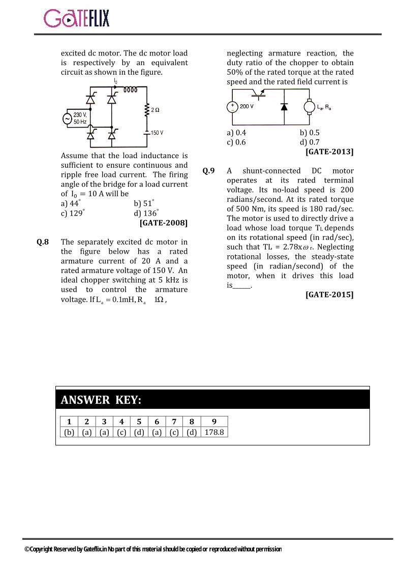
excited dc motor. The dc motor load is respectively by an equivalent circuit as shown in the figure.
Assume that the load inductance is sufficient to ensure continuous and ripple free load current. The firing angle of the bridge for a load current of I0 = 10 A will be a) 44° b) 51°
c) 129° d) 136°
[GATE-2008]
Q.8 The separately excited dc motor in the figure below has a rated armature current of 20 A and a rated armature voltage of 150 V. An ideal chopper switching at 5 kHz is used to control the armature voltage. If a aL 0.1mH,R 1Ω= = ,
neglecting armature reaction, the duty ratio of the chopper to obtain 50% of the rated torque at the rated speed and the rated field current is
a) 0.4 b) 0.5c) 0.6 d) 0.7
[GATE-2013]
Q.9 A shunt-connected DC motor operates at its rated terminal voltage. Its no-load speed is 200 radians/second. At its rated torque of 500 Nm, its speed is 180 rad/sec. The motor is used to directly drive a load whose load torque TL depends on its rotational speed (in rad/sec), such that TL = 2.78xω r. Neglecting rotational losses, the steady-state speed (in radian/second) of the motor, when it drives this load is______.
[GATE-2015]
1 2 3 4 5 6 7 8 9 (b) (a) (a) (c) (d) (a) (c) (d) 178.8
ANSWER KEY:
© Copyright Reserved by Gateflix.in No part of this material should be copied or reproduced without permission
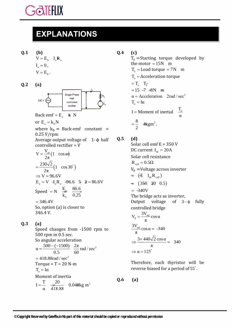
Q.1 (b) b a aV E I R= +
aI 0= ,
bV E= .
Q.2 (a)
Back emf aE k N= = φor a bE k N=where kb = Back-emf constant = 0.25 V/rpm Average output voltage of 1-ϕ half controlled rectifier = V
( )mVV 1 cosα2π
= +
( )°230 2 1 cos302π
= +
V 96.6V⇒ =a a aE V I R 96.6 5 2= − = − × 86.6V=
Speed a
b
E 86.6Nk 0.25
= = =
346.4V= So, option (a) is closer to 346.4 V.
Q.3 (a) Speed changes from -1500 rpm to 500 rpm in 0.5 sec. So angular acceleration
2500 ( 1500) 2πα rad / sec0.5 60− −
= ×
2418.88rad / sec= Torque = T = 20 N-m
aT Iα= Moment of inertia
2T 20I 0.048kg mα 418.88
= = =
Q.4 (c) Ts =Starting torque developed by the motor 15N m= −
LT = Load torque 7N m= −
aT =Acceleration torque
s LT T= −15 7 8N m= − = −
2α Acceleration 2rad / sec= − aT Iα=
aTI Moment of inertialα
= =
28 4kgm2
= = .
Q.5 (d) Solar cell emf E = 350 V DC current dcI 20A= Solar cell resistance
cellR 0.5Ω= V0 =Voltage across inverter
( )dc cellE I R= − −
( )350 20 0.5= − − ×340V= −
The bridge acts as inverter, Output voltage of 3−φ fully controlled bridge
ml0
3VV cosαπ
=
ml3V cosα 340π
= −
3 440 2 cosα 340π
×⇒ = −
°α 125⇒ =
Therefore, each thyristor will be reverse biased for a period of °55 .
Q.6 (a)
EXPLANATIONS
© Copyright Reserved by Gateflix.in No part of this material should be copied or reproduced without permission
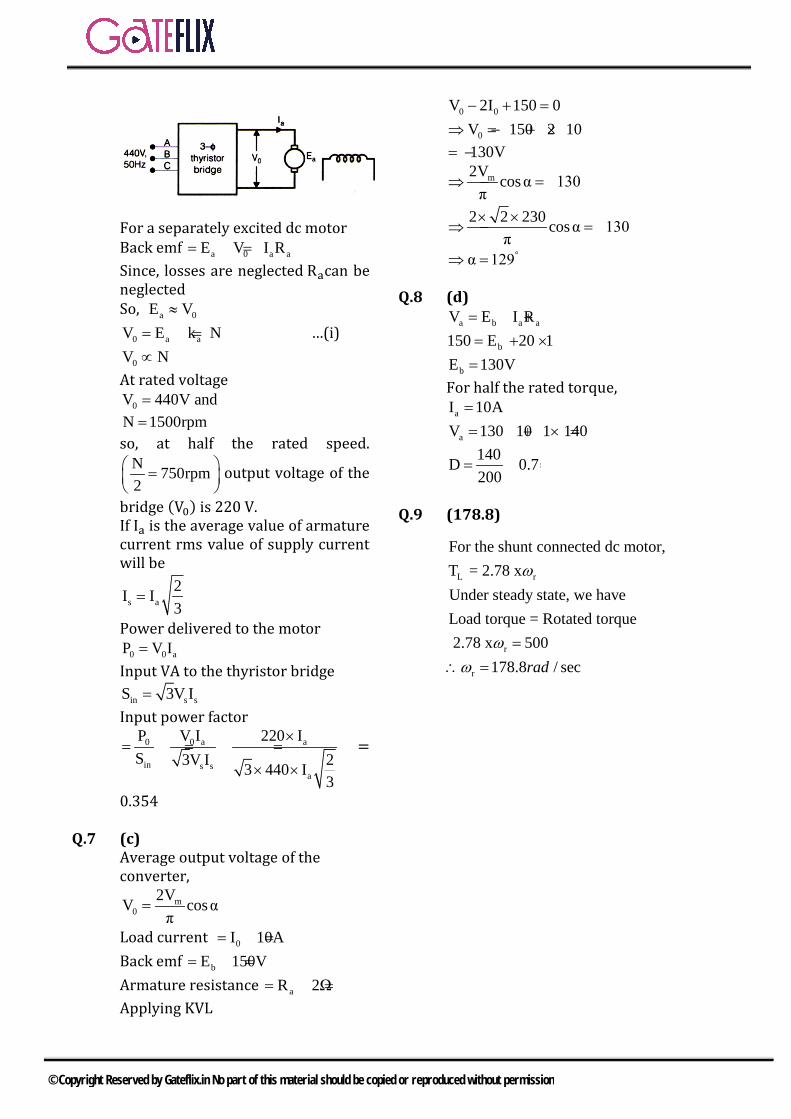
For a separately excited dc motor Back emf a 0 a aE V I R= = −Since, losses are neglected Racan be neglected So, a 0E V≈
0 a aV E k N= = φ …(i)
0V N∝At rated voltage
0V 440V and= N 1500rpm= so, at half the rated speed.
N 750rpm2
=
output voltage of the
bridge (V0) is 220 V. If Ia is the average value of armature current rms value of supply current will be
s a2I I3
=
Power delivered to the motor 0 0 aP V I=
Input VA to the thyristor bridge
in s sS 3V I=Input power factor
0 0 a a
in s sa
P V I 220 IS 3V I 23 440 I
3
×= = =
× ×=
0.354
Q.7 (c) Average output voltage of the converter,
m0
2VV cosαπ
=
Load current 0I 10A= =Back emf bE 150V= =Armature resistance aR 2Ω= =Applying KVL
0 0V 2I 150 0− + =
0V 150 2 10⇒ = − + ×130V= −
m2V cosα 130π
⇒ = −
2 2 230 cosα 130π
× ×⇒ = −
°α 129⇒ =
Q.8 (d) a b a aV E I R= +
b150 E 20 1= + ×
bE 130V=For half the rated torque,
aI 10A=
aV 130 10 1 140= + × = 140D 0.7200
= =
Q.9 (178.8)
L r
r
r
For the shunt connected dc motor,T = 2.78 xUnder steady state, we haveLoad torque = Rotated torque 2.78 x 500
178.8 / secrad
ω
ωω
=∴ =
© Copyright Reserved by Gateflix.in No part of this material should be copied or reproduced without permission
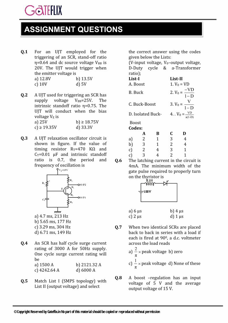
Q.1 For an UJT employed for the triggering of an SCR, stand-off ratio η=0.64 and dc source voltage VBB is 20V. The UJT would trigger when the emitter voltage is a) 12.8V b) 13.5Vc) 10V d) 5V
Q.2 A UJT used for triggering an SCR has supply voltage VBB=25V. The intrinsic standoff ratio η=0.75. The UJT will conduct when the bias voltage VE is a) 25V b) ≥ 18.75Vc) ≥ 19.35V d) 33.3V
Q.3 A UJT relaxation oscillator circuit is shown in figure. If the value of timing resistor RT=470 KΩ and CT=0.01 μF and intrinsic standoff ratio is 0.7, the period and frequency of oscillation is
a) 4.7 ms, 213 Hzb) 5.65 ms, 177 Hzc) 3.29 ms, 304 Hzd) 6.71 ms, 149 Hz
Q.4 An SCR has half cycle surge current rating of 3000 A for 50Hz supply. One cycle surge current rating will be a) 1500 A b) 2121.32 Ac) 4242.64 A d) 6000 A
Q.5 Match List I (SMPS topology) with List II (output voltage) and select
the correct answer using the codes given below the Lists: (V-input voltage, V0–output voltage, D-Duty cycle & a-Transformer ratio); List-I List-II A. Boost 1. V0 = VD
B. Buck 2. V0 =VD
1 D
C. Buck-Boost 3. V0 =V
1 D
D. Isolated Buck- 4. . V0 = VD
a(1-D)
Boost Codes:
A B C D a) 2 1 3 4 b) 3 1 2 4 c) 2 4 3 1 c) 3 4 2 1
Q.6 The latching current in the circuit is 4mA. The minimum width of the gate pulse required to properly turn on the thyristor is
a) 6 μs b) 4 μsc) 2 μs d) 1 μs
Q.7 When two identical SCRs are placed back to back in series with a load if each is fired at 900, a d.c. voltmeter across the load reads
a) 2
πpeak voltage b) zero
c) 1
πpeak voltage d) None of these
Q.8 A boost –regulation has an input voltage of 5 V and the average output voltage of 15 V.
ASSIGNMENT QUESTIONS
© Copyright Reserved by Gateflix.in No part of this material should be copied or reproduced without permission
The duty cycle is
a) 3
2b)
2
3
c) 5
2d)
15
2
Q.9 A load resistance of 10Ω is fed through a 1-phase voltage controller from a voltage source of 200 sin 314 t. For a firing angle delay of 90o, thepower delivered to load in kW, is a) 0.5 b) 0.75c) 1 d) 2
Q.10 A load consisting of R=10Ω and ωL=10Ω, is being fed from 230V, 50Hz source through a 1-phase voltage controller. For a firing angle delay of 30o, the rms value of load current would be
a) 23A b) 23/ 2 A
c) >23/ 2 A d) <23/ 2 A
Q.11 A single phase voltage controller feeds power to a resistance of 10Ω. The source voltage is 200V rms. For a firing angle of 90o, the rms value of thyristor current in amperes is a) 20 b) 15c) 10 d) 5
Q.12 A single-phase voltae controller is employed for controlling the power flow from 260 V, 50Hz source into a load consisting of R=5Ω and ωL=12Ω. The value of maximum rms load current and the firing angle are respectively a) 20 A, 0o
b) 260/10.91 A, 0o
c) 20A, 90o
d) 260/10.91A, 90o
Q.13 In a single phase voltage controller with RL load, ac output power can be controlled if a) firing angle α>Ø(load phase
angle) and conduction angle γ=π
b) α>Ø and γ<πc) α<Ø and γ=πd) α<Ø and γ>π
Q.14 A single phase voltage controller feeds power to a resistance of 10Ω. The source voltage is 200V rms. For a firing angle of 90o, the rms value of thyristor current in amperes is a) 20 b) 15c) 10 d) 5
Q.15 A single-phase voltage controller is connected to a load of resistance 10Ω and a supply of 200 sin 314t volts. For a firing angle of 90o, the average thryristor current in amperes is
a) 10/π b) 10 2
c) 5 2 /π d) 5 2
Q.16 A thyristor is triggered by a pulse train of 5 KHz. The duty ratio is 0.4. If the allowable average power is 100W, the maximum allowable gate drive power is
a) 50W b) 100 2 Wc) 150W d) 250W
Q.17 For a single-phase half-bridge, amplitude of output voltage is V, and the output power is P. Then their corresponding values for a single phase full-bridge inverter are a) Vs, P b) Vs/2, P/2c) 2V, 4P d) Vs, 2P
Q.18 A half wave SCR controlled circuit with XL 50Ω conducts for 90o for an applied voltage of 800V sinusoidal rms.If the SCR voltage drop is negligible, the power dissipated by the load is a) 1800W b) 81Wc) 52.36W d) 0W
Q.19 In the circuit shown in the figure L=5μH and C=20μF, C is initially changed to 200V. After the switch S
© Copyright Reserved by Gateflix.in No part of this material should be copied or reproduced without permission
is closed at t=0, the maximum value of current and the time at which it reaches this value are respectively a) 100A, 15.707 μsb) 50 A, 30μsc) 100A, 62.828μsd) 900 A, 31.414μs
Q.20 The fundamental ripple frequency of a six pulse circuit with supply frequency 50 Hz is a) 100 Hz b) 200 Hzc) 300 Hz d) 600 Hz
Q.21 Output voltage of a single-phase full converter has peak value of 300 V and average value of 120 V then firing angle will be a) 300 b) 510
c) 1300 d) 1500
Q.22 A voltage source 200 sin 314t is applied to a thyristor controlled half wave rectifier with resistive load of 50 . If the firing angle is 300 with respect to supply voltage waveform, the average power in the load is a) 90.6 watts b) 194 wattsc) 60.8 watts d) 70.6 watts
Q.23 In single-phase full-wave controlled bridge rectifier, minimum output voltage is obtained at conduction angle………………..and maximum at conduction angle………….. a) 00, 1800 b) 1800, 00
c) 00, 00 d) 1800, 1800
Q.24 In a single phase full converter bridge, average output voltage is
a) α-π/2
mα+π/2
1V cos θdθ
π
b) α+π/2
mα-π/2
1V cosθ dθ
π
c) π+α
mα
1V cosθ d θ
π
d) α+π
m0
1V cos θ dθ
π
Q.25 In a 1ϕhalf wave controlled rectifier if input voltage is 400 sin 314 t, the average output voltage for a firing angle of 600 is
a) 100
πb)
200
π
c) 300
πd)
400
π
Q.26 In a 1ϕfull converter, for load current I ripple free, average thysistor current is
a) 1
I4
b) 1
I2
c) 3
I4
d) I
Q.27 In a 1ϕfull converter, number of SCRs conducting during overlap: a) 2 b) 4c) 6 d) 8
Q.28 For an n-pulse rectifier, the rms value of the ac current is related to the dc load current as
a) Irms = Id/n b) drms
II
n
c) rms dI I d) rms d
2I I
Q.29 In a single–phase semi converter, with discontinuous conduction and extinction angle <π, freewheeling action takes phases for a) b) π - c) - π d) Zero degree
Q.30 In a 3-phase bridge rectifier fed from the star connected secondary winding of a transformer, let the voltage to the neutral of the A-phase (phase sequence A, B, C) be Vm sin t. At the instant when the voltage ofA-phase is maximum, the output voltage at the rectifier terminals will be
© Copyright Reserved by Gateflix.in No part of this material should be copied or reproduced without permission
a) mV
2b) m3V
c) m1.5V d) m3 V
Q.31 A single–phase full–bridge converter with a free–wheeling diode feeds an inductive load. The load resistance is 15.53 and it has large inductance providing constant and ripple free d.c. current. Input to converter is form an ideal 230 V, 50 Hz single phase source. For a firing delay angle of 60o, the average value of diode currents is a) 10 A b) 8.165 Ac) 5.774 A d) 3.33 A
Q.32 In a three- phase full wave a.c. to d.c. converter, the ratio of output ripple- frequency to the supply – voltage frequency is a) 2 b) 3c) 6 d) 12
Q.33 If the r.m.s. source voltage is V volts, the minimum and maximum values of firing angle for a single-phase, half-wave controlled rectifier, supplying a load with a back e.m.f. of 40 volts are a) 0o and 180o
b) 1 040sin and180
2V
c) -1 -140 40α=sin and π-sin .
2V 2V
d) 0o and 1 40sin
2V
Q.34 A single phase bridge inverter delivers power to a series connected RLC load with R=2Ω, ωL=8Ω. For this inverter-load combination, load commutation is possible in case the magnitude of ωC in ohms is a) 10 b) 8c) 6 d) zero
Q.35 For a 3-phase bridge inverter in 180o conduction mode, figure below, the sequence of SCR conduction in the first two steps, beginning with the initiation of thyristor 1, is a) 6, 1, 2 and 2, 3, 1b) 2, 3, 1 and 3, 4, 5c) 3, 4, 5 and 5, 6, 1d) 5, 6, 1 and 6, 1, 2
Q.36 In single-pulse modulation of PWM inverters, third harmonic can be eliminated if pulse width is equal to a) 30o b) 60o
c) 120o d) 150o
Q.37 In single-pulse modulation of PWM inverters, fifth harmonic can be eliminated if pulse width is equal to a) 30o b) 72o
c) 36o d) 108o
Q.38 In single-pulse modulation of PWM inverters, the pulse width is 120o. For an input voltage of 220 V dc, the r.m.s. value of output voltage is a) 179.63 V b) 254.04 Vc) 127.02V d) 185.04V
Q.39 In single-pulse modulation used in PWM inverters, Vs is the input dc voltage. For eliminating third harmonic, the magnitude of rms values of fundamental component of output voltage and pulse width are respectively
a) (2 2 /π) Vs, 120o
b) (4Vs/π), 60o
c) (2 2 /π) Vs, 60o
d) (4Vs/π), 120o
Q.40 In multiple-pulse modulation used in PWM inverters, the amplitude of reference square wave and triangular carrier wave are respectively 1V and 2V. For generating 5 pulses per half cycle, the pulse width should be a) 36o b) 24o
c) 18o d) 12o
© Copyright Reserved by Gateflix.in No part of this material should be copied or reproduced without permission
Q.41 In multiple-pulse modlation used in PWM inverters, the amplitude and frequency for triangular carrier and square reference signals are respectively 4V, 6KHz and 1V, 1KHz. The number of pulses per half cycle and pulse width is respectively a) 6, 90o b) 3, 45o
c) 4, 60o d) 3, 40o
Q.42 In sinusoidal-pulse modulation used in PWM inverters, amplitude and frequency for triangular carrier and sinusoidal reference signals are respectively 5V, 1KHz and 1V, 50Hz. If zeros of the triangular carrier and reference sinusoid coincide, then the modulation index and order of significant harmonics are respectively a) 0.2, 9 and 11b) 0.4, 9 and 11c) 0.2, 17 and 19d) 0.2, 19 and 21
Q.43 In an inverter with fundamental output frequency of 50Hz, if third harmonic is eliminated, then frequencies of other components in the output voltage wave, in Hz, would be a) 250, 350, 450, high frequenciesb) 50, 250, 350, 450c) 50, 250, 350, 550d) 50, 100, 200, 250
Q.44 In single pulse modulated PWM inverter, third harmonic, is eliminated by making pulse width equal to 1200, the eliminate fifth harmonic the pulse width be equal to a) 360 b) 720
c) 1090 d) 1440
Q.45 Full- bridge inverter is shown in the above fig. The maximum rms output voltage ‘V0’ at fundamental frequency is
a) 24V b) 33.94Vc) 43.3V d) 48V
Q.46 A single – phase full – bridge voltage source inverter operating in square wave mode supplies a purely inductive load. If the inverter time period is T, then the time duration for which the feedback diodes conduct in a cycle is a) T b) T/2c) T/4 d) T/8
Q.47 For a single phase, full-bridge inverter supplying power to a highly inductance load as shown above, the correct sequence of operations of switches and diodes is
a) S1-S4 – S3-S2 - S1-S4- S3-S2
b) D1-D4 – S1-S4 – D2-D3- S2-S3
c) S1-D3 – S1-S4 – S4-D2- D2-D3
d) S2-D4 – D4-D1 - D1-S3- S3-S2
Q.48 A single–phases, half-bridge inverter has input voltage of 48 VDC. Inverter is feeding a load of 2.4. The r.m.s. output voltage at fundamental frequency is
a) 2 48V
b)
2 48V
2
c)2 48V
d)48V
2 2
Q.49 A d.c. source is switched in steps to synthesize the three- phase output. The basic three-phase bridge inverter can be controlled. The angle through which each switch conducts and at any instant the number of swatches conducting simultaneously is respectively a) 120o and 02 b) 120o and 03c) 180o and 02 d) 180o and 04
© Copyright Reserved by Gateflix.in No part of this material should be copied or reproduced without permission

Q.50 The number of thyristors required for single-phaseto single-phase cycloconverter of the mid-point type and for three phase to three-phase 3-pulse type cycloconverter are respectively a) 4, 6 b) 8, 18c) 4, 18 d) 4, 36
Q.51 A 3-phase to single-phase converters device employs a 6-pulse bridge cycloconverter. For an input voltage of 200V per phase, the fundamental rms value of output voltage is
a) 600/πV b) 300 3 /πV
c) 300/πV d) 600 2 /πV
Q.52 In a single – phase to single – phase cycloconverter, if 1 and 2 are the trigger angles of positive converter and negative converter, then
a) 1 + 2 =2
b) 1 + 2 = π
c) 1 + 2 =3
2
d) 1 + 2 = 2π
Q.53 A cycloconverter is operating on a 50Hz supply. The range of output frequency that can be obtained with acceptable quality, is a) 0-16Hz b) 0-32Hzc) 0-64Hz d) 0-128Hz
Q.54 A 3-phase cycloconverter is used to obtain a variable –frequency single-phase a.c. output. The single phase a.c. load is220 V, 60 A at a power factor of 0.6 lagging. The rms value of input voltage per phase required is a) 376.2 V b) 311.12 Vc) 266 V d) 220 V
Q.55 Three-phase to three phase cycloconverters employing 18 SCRs and 36 SCRs have the same voltage and current ratings for their component thyristor. The ratio of
VA rating of 36-SCR device to that of 18-SCR is a) ½ b) 1c) 2 d) 4
Q.56 Three-phase to 3-phase cycloconverters employing 18SCRs and 36 SCRs have the same voltage and current ratings for their component thyristors. The ratio of powerhandled by 36-SCR device to that handled by 18-SCR device is a) 4 b) 2c) 1 d) ½
Q.57 For type-A chopper, Vs is the source voltage, R is the load resistance and α is the duty cycle. The average output voltage and current for this chopper are respectively a) αVs, α.(Vs/R)b) (1-α)Vs, (1-α)Vs/Rc) Vs/α, Vs/αRd) Vs/(1-α), Vs/(1-α)R
Q.58 A chopper has Vs as the source voltage, R as the load resistance and α as the duty cycle. For this chopper, rms value of output voltage is
a) αVs b) . Vs
c) Vs/ d) 1 .Vs
Q.59 For a chopper, Vs is the source voltage, R is the load resistance and α is duty cycle. RMS and average values of thyristor currents for this chopper are
a) α.(Vs/R), .(Vs/R)
b) . (Vs/R), .(Vs/R)
c) Vs/R, α Vs/R
d) 1 .(Vs/R), (1- α)Vs/R
Q.60 In dc choppers, per unit ripple is maximum when duty cycle α is a) 0.2 b) 0.5c) 0.7 d) 0.9
© Copyright Reserved by Gateflix.in No part of this material should be copied or reproduced without permission
Q.61 For type-A chopper; Vs, R, I0 and α are respectively the dc source voltage, load resistance, constant load current and duty cycle. For this chopper, average and rms values of freewheeling diode currents are
a) α I0, . I0
b) (1-α) I0, 1 . I0
c) α .(Vs/R), .(Vs/R)
d) (1-α) I0, . I0
Q.62 A step-up chopper has Vs as the source voltage and α as the duty cycle. The output voltage for this chopper is given by a) Vs(1+α) b) Vs/(1-α)c) Vs(1-α) d) Vs/(1+α)
Q.63 When a series LC circuit is connected to adc supply of V volts through a thyristor, then the peak current through thyristor is
a) V. LC b) V/ CL
c) V. C / L d) V. L / C
Q.64 For the arrangement shown in figure, the circuit is initially in steady state with thyristor T off. After thyristor T is turned on, the peak thyristor current would be a) 2A b) 22Ac) 40A d) 42A
Q.65 In type-A chopper, source voltage is 100V dc, on period = 100 μs, off period = 150 μs and load RLE consists of R = 2Ω, L=5mH, E=10V. For continuous conduction, average output voltage and average output current for this chopper are respectively: a) 40V, 15A b) 66.66V, 28.33Ac) 60V, 25A d) 40V, 20A
Q.66 In a two-quadrant dc to dc chopper, the load voltage is varied positive maximum to negative maximum by
varying the time ratio of the chopper from a) Zero to units b) Unity to zeroc) Zero to 0.5 d) 0.5 to Zero
Q.67 A step up chopper is fed from a 220 V dc source to deliver a load voltage of 660 V. If the non-conduction time of the thyristor is 100 μs, the required pulse width will be a) 100 μs b) 300μsc) 200μs d) 660 μs
Q.68 In dc choppers, if Ton is the on-period and f is the chopping frequency, then output voltage in terms of input voltage Vs is given by a) Vs. Ton/f b) Vs. f/Ton
c) Vs/f. Ton d) Vs. f. Ton
Q.69 A 3- phase wound rotor inductance motor is controlled by a chopper – controlled resistance in its rotor circuit. A resistance of 2 is connected in the rotor circuit and a resistance of 4 is additionally connected during OFF periods of the chopper. The OFF period of the chopper is 4 ms. The average resistance in the rotor circuit for the chopper frequency of 200 Hz is
a) 26
5 b)
24
5
c) 18
5 d)
16
5
Q.70 For a step up d.c. – d.c. chopper with an input d.c. voltage of 220 volts, if the output voltage require is 330 volts and the non-conducting time of thyristor is 100 μs the ON time thyristor would be a) 66.6 μs b) 100 μsc) 50 μs d) 200 μs
Q.71 Duty cycle in a chopper circuit with switching frequency 100 Hz and TON time as 2 ms a) 0.2 b) 0.4c) 0.8 d) none
© Copyright Reserved by Gateflix.in No part of this material should be copied or reproduced without permission

Q.72 A step up chopper is connected to 100 V d.c. supply. For a duty cycle of 0.5 the output voltage in volts will be
a)100
1.5b) 50
c) 150 d) 200
Q.73 A d.c. chopper is fed from a 100 V d.c. source. Its output voltage is rectangular pulses of duration 1 millisecond in overall cycle time of 3millisecond. Its ripple factor will be 2, the average output voltage in volts will be a) 25 b) 33.3c) 50 d) 66.6
Q.74 A LC series circuit is connected to a d.c. supply of 100 V through a thyristor, the peak current through the thyristor will be
a) 100 ( LC ) b) 100
LC
c) 100 L
C
d) 100 C
L
Q.75 If the chopper switching frequency is 200 Hz and ton time is 2ms, the duty cycle is a) 0.4 b) 0.8c) 0.6 d) none of the above
1 2 3 4 5 6 7 8 9 10 11 12 13 14
(b) (c) (b) (b) (b) (b) (b) (b) (c) (b) (b) (a) (a) (c)
15 16 17 18 19 20 21 22 23 24 25 26 27 28
(a) (d) (c) (d) (a) (c) (b) (b) (a) (b) (c) (b) (b) (b)
29 30 31 32 33 34 35 36 37 38 39 40 41 42
(d) (c) (d) (c) (c) (a) (d) (c) (b) (a) (a) (c) (b) (c)
43 44 45 46 47 48 49 50 51 52 53 54 55 56
(c) (b) (c) (b) (b) (c) (a) (c) (b) (b) (a) (c) (c) (a)
57 58 59 60 61 62 63 64 65 66 67 68 69 70
(a) (b) (a) (b) (b) (c) (c) (b) (a) (d) (b) (d) (a) (c)
71 72 73 74 75
(a) (d) (b) (d) (a)
ANSWER KEY:
© Copyright Reserved by Gateflix.in No part of this material should be copied or reproduced without permission
Q.1 (b) UJT triggering η 0.64
BBV 20v
E BB DV ηV V
0.64 20 0.7 13.5V
Q.2 (c) UJT triggering η 0.75
BBV 25v
E BB DV ηV V
0.75 25 0.7
19.35
Q.3 (b) UJT relaxation oscillator
TR 470kΩ
TC 0.01μF,η 0.7
c
lT R ln
l n
3 6 1470 10 0.01 10 ln
1 0.7
5.65ms
1 1f 176.7Hz
T 5.65ms
Q.4 (b) Half cycle surge current = 3000A= isb Equalizing the charge balance eqn
2 2
sbI T I t
t duration;
T half cycle duration
2 21 1I (3000)
100 200
1I 3000.
2
2121.32A
Q.5 (b) Buck oV VD
Boost V
1 D
Buck-Boost VD
1 D
Isolated buck-Boost VD
a 1 D
Q.6 (b) Latching current Lat4mA I
When Thyristor is conducting (or to start conduction) Thyristor anode current =Latching current
diL v
dt
Lat
on
IL 100
t
on
0.1 4mt
100
4μs
Q.7 (b) Two identical SCRs are placed back to back 90 If DC voltammeter connected across load. The voltmeter connected load the voltmeter reads zero +ve half cycle =-ve half cycle
EXPLANATIONS
© Copyright Reserved by Gateflix.in No part of this material should be copied or reproduced without permission
Q.8 (b) Boost converter, Input voltage
sV 5v ,
Output voltage ,oV 15
The relationship between Input & Output voltage is
o s
s o
V V11 D
V 1 D V
o s
o
V V 15 5 10 2D
V 15 15 3
Q.9 (c) 1 ΦAc voltage controller
R 10Ω v 200sin314t
90°
π
2 2 2
rms m
1v v sin ωt d ωt
π
π2
mv 1 cos 2ωtd ωt
π 2
2
mv sin 2π
2π 2
1
2
rms m
π 90°V V
2π
mV100
2
Power delivered to Load 2
rmsv 100 100
R 10
= 1 KW
Q.10 (b)
LR 10Ω &X 10Ω
sV 230v, 30° 1/2
or s
π sin 2V V
π 2π
1/2
ππ
sin 606230π 2π
226v 230v
oror
2 2
V 230I
z 10 10
23A
2
Q.11 (b) R 10Ω
sV 200v, 90° 1/2
or s
π sin 2V V
π 2π
sV 200141.42v
2 2
oror
V 141.42I
R 10
14.2A
Q.12 (a) 1 ΦAc voltage controller
sV 260v
R 5ΩwL 12Ω At 90°
2 2z R wL
25 144
13Ω
max
260 2I 20 2A at 0°
13
At mrms
v0° V 260v
2
rms
260I 20A
13
Q.13 (a) 1 ΦAcvoltage controller with RL Load
The control range is Φ & π ΦImpedance Angle &
tan−1 WL
R
Conduction angle r π π
Q.14 (c)
© Copyright Reserved by Gateflix.in No part of this material should be copied or reproduced without permission
1 ΦAc voltage controller
R 10Ω
sV 200v, 90° 1/2
or m
πV V if 90°
2π
1/2
1/2
m m
ππ
12V V2π 4
200 2100 2
2
or
100 2I 10 2
10
RMS Thyristor current π
2 2
TA or
1I I dt
2π
2
TA
1 πI .200. π 100
2π 2
TAI 10A
Q.15 (a) R 10Ω V 200Sin314t
90° Average Thyristor
π
m
1V sinwt d(wt)
2πR
mV(1 cos )
2πR
mV 200
2πR 2 π 10
10A
π
Q.16 (d) Thyristor is triggered by pulse train f 5KHz D 0.4
gavP 100ω
gm on gavP .T P .T
gav
gm
on
P .TP
T
gavP
8
gm
100P 250W
0.4
Q.17 (c) Single phase Half wave
mdc
Vv
π
Full wave mdc
2Vv
π
V fw 2V(Hw)
Power 2v
P Fw 4P(Hw)
Q.18 (d) Half wave SCR controlled
LX 50Ω
90° V 800(rms)
Power dissipated =0 ( L acts as short circuit to Dc )
Q.19 (a) L 5μH
C 20μF
V 200v
s o
Ci t v sin ω t
L
65
o o
1 10 πω 10 ,peak atω t
10 2LC
6
π 10t 15.71us
2 10
cp s
Ci v
L
5 200200 100A
20 2
© Copyright Reserved by Gateflix.in No part of this material should be copied or reproduced without permission
Q.20 (c) Six pulse converter
sf 50Hz
Output ripples6f 6 50 300Hz
Q.21 (b) 1 ΦFull wave converter
dcv 120v
mV 300v
Firing ?
mdc
2Vv cos
π
120 πcos
2 300
0.6283 51°
Q.22 (b) Half wave rectifier
sV 200sin314t
R 50Ω 30°
π
2 2 2
rms m
1v v sin ωt d ωt
2π
1/2
rms m
π sin 2V V
4π 8π
1/2
rms
ππ
sin 606V 2004π 8π
1/2
200 0.208 0.035
98.4v 2
rmsVP 194watts
R
Q.23 (a) 1 ΦFull wave rectifier
mdc
2Vv cos
π
o 90,The converter mode
90 180°,
The inverter mode
mdc
2V 0 v
π
mdc
2V 180° v
π
Q.24 (b) 1 ΦFull wave converter
2
dc m
2
1v = V cosθdθ
π
π
π
m 2
2
Vsinθ |
π
π
π
mV π πsin sin
π 2 2
mV πcos sin
π 2
m2Vcos
π
Q.25 (c) 1 Φ Half wave controlled rectifier
sv =400sin314t
60°
mdc
Vv = (1 cos )
2π
= 400
1 cos602
π
400 3 300= . =
2π 2 π
Q.26 (b) 1-ΦFull converter Load Current =I
T(avg)
1I = Idt
2π π
o
I=
2
Q.27 (b)
© Copyright Reserved by Gateflix.in No part of this material should be copied or reproduced without permission
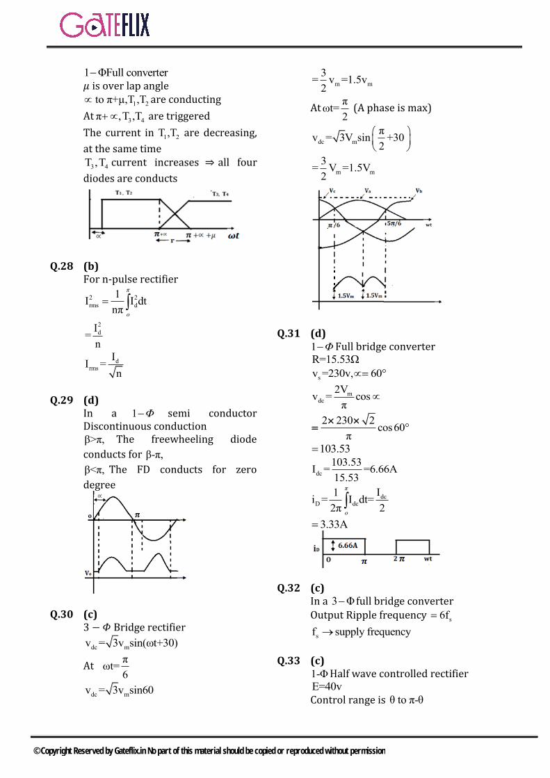
1 ΦFull converter 𝜇 is over lap angle
1 2to π+µ,T ,T are conducting
At 3 4π ,T ,T are triggered
The current in 1 2T ,T are decreasing,
at the same time
3 4T ,T current increases ⇒ all four
diodes are conducts
Q.28 (b) For n-pulse rectifier
2 2
rms d
1I I dt
nπ
π
o
2
dI=
n
drms
II =
n
Q.29 (d) In a 1Φ semi conductor Discontinuous conduction β>π, The freewheeling diode
conducts for β-π,
β<π, The FD conducts for zero
degree
Q.30 (c) 3 − 𝛷 Bridge rectifier
dc mv = 3v sin(ωt+30)
At π
ωt=6
dc mv = 3v sin60
m m
3= v =1.5v
2
Atπ
ωt=2
(A phase is max)
dc m
πv = 3V sin +30
2
m m
3= V =1.5V
2
Q.31 (d) 1Φ Full bridge converter R=15.53Ω
sv =230v, 60°
mdc
2Vv = cos
π
2 230 2cos60°
π
103.53
dc
103.53I = =6.66A
15.53
dcD dc
I1i = I dt=
2π 2π
o
3.33A
Q.32 (c) In a 3 Φ full bridge converter Output Ripple frequency s6f
sf supply frequency
Q.33 (c) 1-Φ Half wave controlled rectifier E=40v Control range is θ to π-θ
© Copyright Reserved by Gateflix.in No part of this material should be copied or reproduced without permission
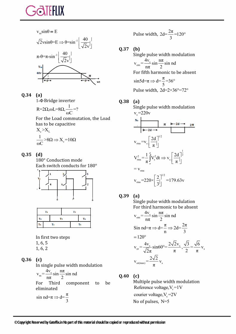
mv sinθ E
-1 402vsinθ=E θ=sin
2v
-1 40π-θ=π-sin
2v
Q.34 (a) 1-Φ Bridge inverter
1R=2Ω,ωL=8Ω, =?
ωC
For the Load commutation, the Load has to be capacitive
c LX >X
c
1>8Ω X =10Ω
ωC
Q.35 (d) 180° Conduction mode Each switch conducts for 180°
In first two steps 1, 6, 5 1, 6, 2
Q.36 (c) In single pulse width modulation
sm
4v nπv = sin sin nd
nπ 2
For Third component to be eliminated
πsin nd=π d=
3
Pulse width, 2π
2d= =120°3
Q.37 (b) Single pulse width modulation
som
4v nπv = sin sin nd
nπ 2
For fifth harmonic to be absent π
sin5d=π d= =36°5
Pulse width, 2d=2×36°=72°
Q.38 (a) Single pulse width modulation
sv =220v
1/2
rms s
2dv =v
π
1
22 2
rms s s
1 2dV = V dt v
π π
π
o
rms= v
1/2
rms
2v =220× =179.63v
3
Q.39 (a) Single pulse width modulation For third harmonic to be absent
som
4v nπv = sin sin nd
nπ 2
π 2πSin nd=π d= 2d=
n 3
120°
s sor s
4v 2 2v 3 6v = sin60°= , = v
π 2 π2π
or(max) s
2 2v = v
π
Q.40 (c) Multiple pulse width modulation
rReference voltage,V =1V
ccourier voltage,V =2V
No of pulses, N=5
© Copyright Reserved by Gateflix.in No part of this material should be copied or reproduced without permission
r
c
V2d π 1 π π= 1- = 1- =
N V N 2 5 10
18°
Q.41 (b) In multiple pulse width modulation Triangular carrier frequency,
cf =6KHz
Amplitude cv =4v
Square reference frequency
rf =1KHz
Amplitude cr
r
f 6v =1vN= = =3
2f 2×1
r
c
V2d π 1 π= 1- = 1-
N V N 4 3
3π π= = =45°
4×3 4
Q.42 (c)
Sinusoidal pulse width modulation Carrier amplitude cv =5v
Frequency, cf =1KHz
Reference amplitude, rv =1v
Frequency, rf =50Hz
The sine and triangular wave zero crossings are matchinz
c
r
f 1000N 1 1
2f 2 100
= 9
Significant Harmonics 2N 1 2 9 1 17,19
Q.43 (c) Fundamental output frequency =50Hz Third harmonic is eliminated
som
4v nπv = sin sinnd
nπ 2
πSin3d=0 d= =60°
3
2π2d= =120°
3
5th harmonic, sin5 60 sin300 finite 7th harmonic, sin7 60 sin 420 finite 9th harmonic, sin9 60 sin540
zero(absent)
11th harmonic, sin11 60 sin660
finite Frequencies in output: 50,250,350,550…..
Q.44 (b) 2d 120° for 3rd harmonic
som
4v nπv = sin sin nd
nπ 2
For 5th harmonic to be eliminated π
sinnd=π 5d=π d=n
2π2d= 72°
5
Q.45 (c) rmv value of output voltage
so1
4vV =
2π
2× 2×48=
π
=43.3v
Q.46 (b) A1 Φ full bridge inverter
Each diode pair conducts of T
4
© Copyright Reserved by Gateflix.in No part of this material should be copied or reproduced without permission
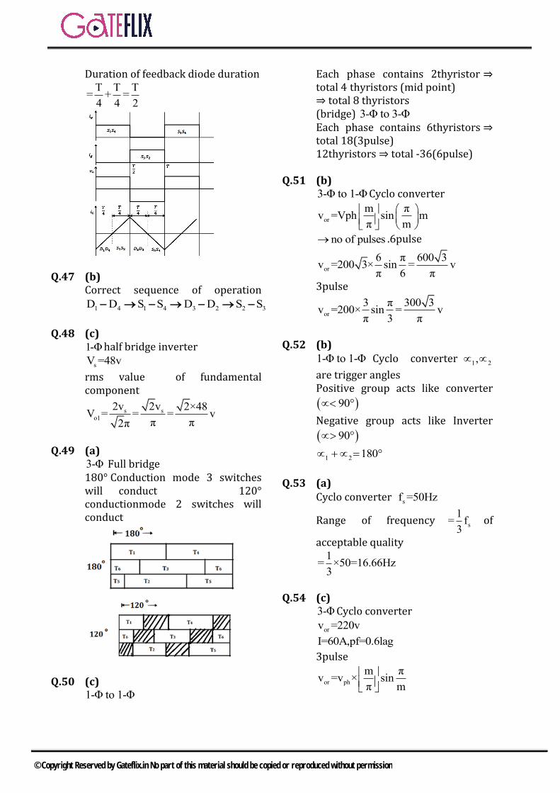
Duration of feedback diode duration T T T
= + =4 4 2
Q.47 (b) Correct sequence of operation
1 4 1 4 3 2 2 3D D S S D D S S
Q.48 (c) 1-Φ half bridge inverter
sV =48v
rms value of fundamental component
s so1
2v 2v 2×48V = = = v
π π2π
Q.49 (a) 3-Φ Full bridge 180° Conduction mode 3 switches will conduct 120° conductionmode 2 switches will conduct
Q.50 (c) 1-Φ to 1-Φ
Each phase contains 2thyristor ⇒ total 4 thyristors (mid point) ⇒ total 8 thyristors(bridge) 3-Φ to 3-Φ Each phase contains 6thyristors ⇒ total 18(3pulse) 12thyristors ⇒ total -36(6pulse)
Q.51 (b) 3-Φ to 1-Φ Cyclo converter
or
m πv =Vph sin m
π m
no of pulses .6pulse
or
6 π 600 3v =200 3× sin = v
π 6 π
3pulse
or
3 π 300 3v =200× sin = v
π 3 π
Q.52 (b) 1-Φ to 1-Φ Cyclo converter 1 2,
are trigger angles Positive group acts like converter
90°
Negative group acts like Inverter
90°
1 2 180°
Q.53 (a) Cyclo converter sf =50Hz
Range of frequency s
1= f
3 of
acceptable quality 1
= ×50=16.66Hz3
Q.54 (c) 3-Φ Cyclo converter
orv =220v
I=60A,pf=0.6lag
3pulse
or ph
m πv =v × sin
π m
© Copyright Reserved by Gateflix.in No part of this material should be copied or reproduced without permission
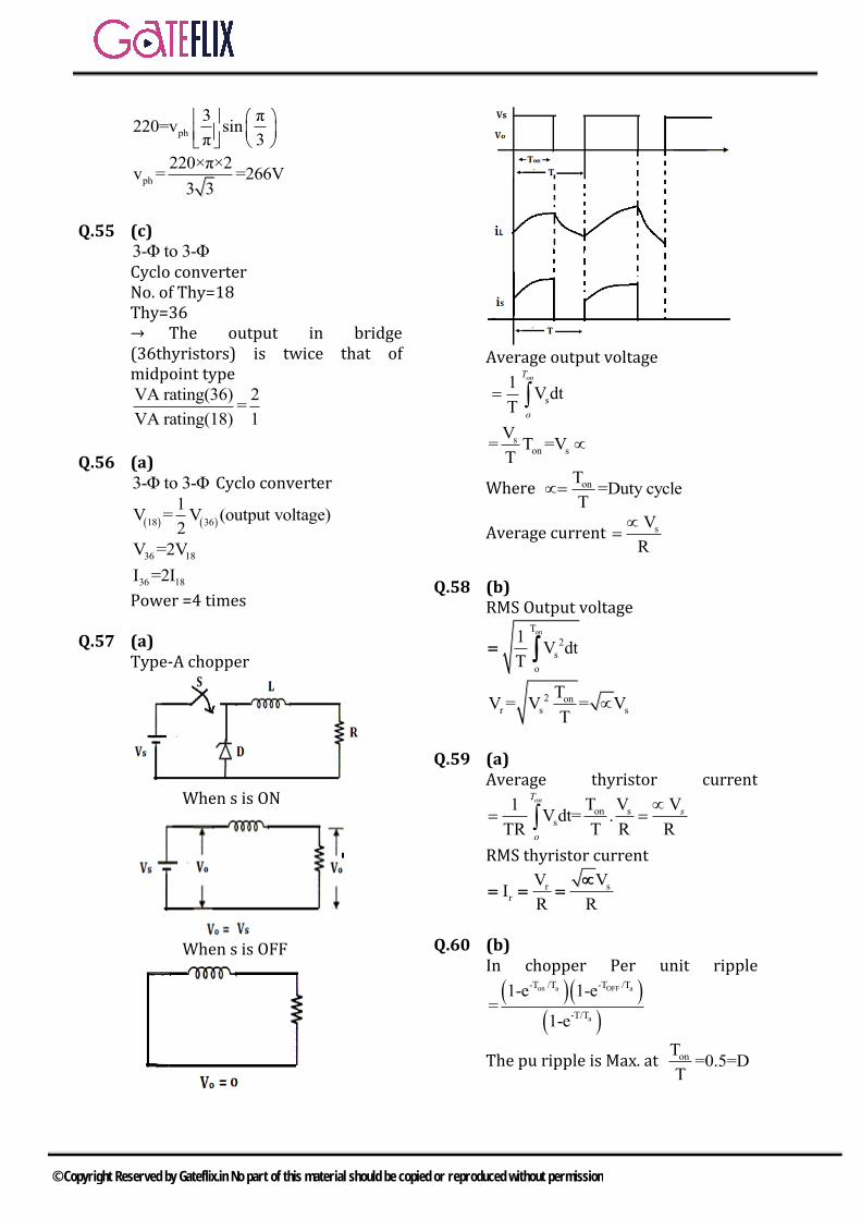
ph
3 π220=v sin
π 3
ph
220×π×2v = =266V
3 3
Q.55 (c) 3-Φ to 3-Φ Cyclo converter No. of Thy=18 Thy=36 → The output in bridge (36thyristors) is twice that of midpoint type VA rating(36) 2
=VA rating(18) 1
Q.56 (a) 3-Φ to 3-Φ Cyclo converter
18 36
1V = V (output voltage)
2
36 18V =2V
36 18I =2I
Power =4 times
Q.57 (a) Type-A chopper
When s is ON
When s is OFF
Average output voltage
s
1V dt
T
onT
o
son s
V= T =V
T
Where onT=Duty cycle
T
Average current sV
R
Q.58 (b) RMS Output voltage
onT
2
s
o
1V dt
T
2 onr s s
TV = V = V
T
Q.59 (a) Average thyristor current
on ss
T V V1V dt= .
TR T R R
onT
s
o
RMS thyristor current
srr
VVI
R R
Q.60 (b) In chopper Per unit ripple
on a OFF a
a
-T /T -T /T
-T/T
1-e 1-e=
1-e
The pu ripple is Max. at onT=0.5=D
T
© Copyright Reserved by Gateflix.in No part of this material should be copied or reproduced without permission
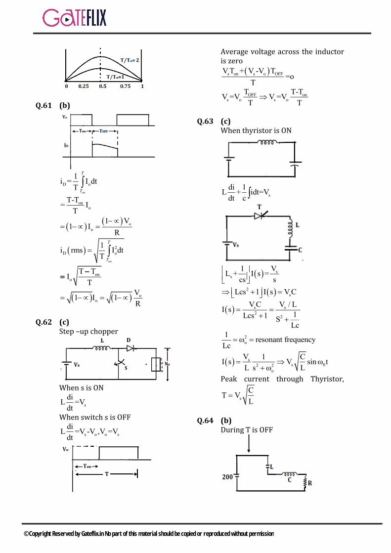
Q.61 (b)
D o
1i = I dt
T on
T
T
ono
T-T= I
T
o
1 V1 I
R
o
2
D o
1i rms I dt
T
on
T
T
on
o
T TI
T
oo
V1 I 1
R
Q.62 (c) Step –up chopper
When s is ON
s
diL =V
dt
When switch s is OFF
s o o s
diL =V -V ,V =V
dt
Average voltage across the inductor is zero
s on s o OFFV T + V -V T=o
T
OFF ons o s o
T T-TV =V V =V
T T
Q.63 (c) When thyristor is ON
s
di 1L + idt=V
dt c
ss
V1L + I s =
cs s
2
sLcs 1 I s V C
s s
22
V C V / LI s
1Lcs 1S
Lc
2
o
1ω resonant frequency
Lc
ss 02 2
o
V 1 CI s V sin ω t
L s ω L
Peak current through Thyristor,
s
CT V
L
Q.64 (b) During T is OFF
© Copyright Reserved by Gateflix.in No part of this material should be copied or reproduced without permission
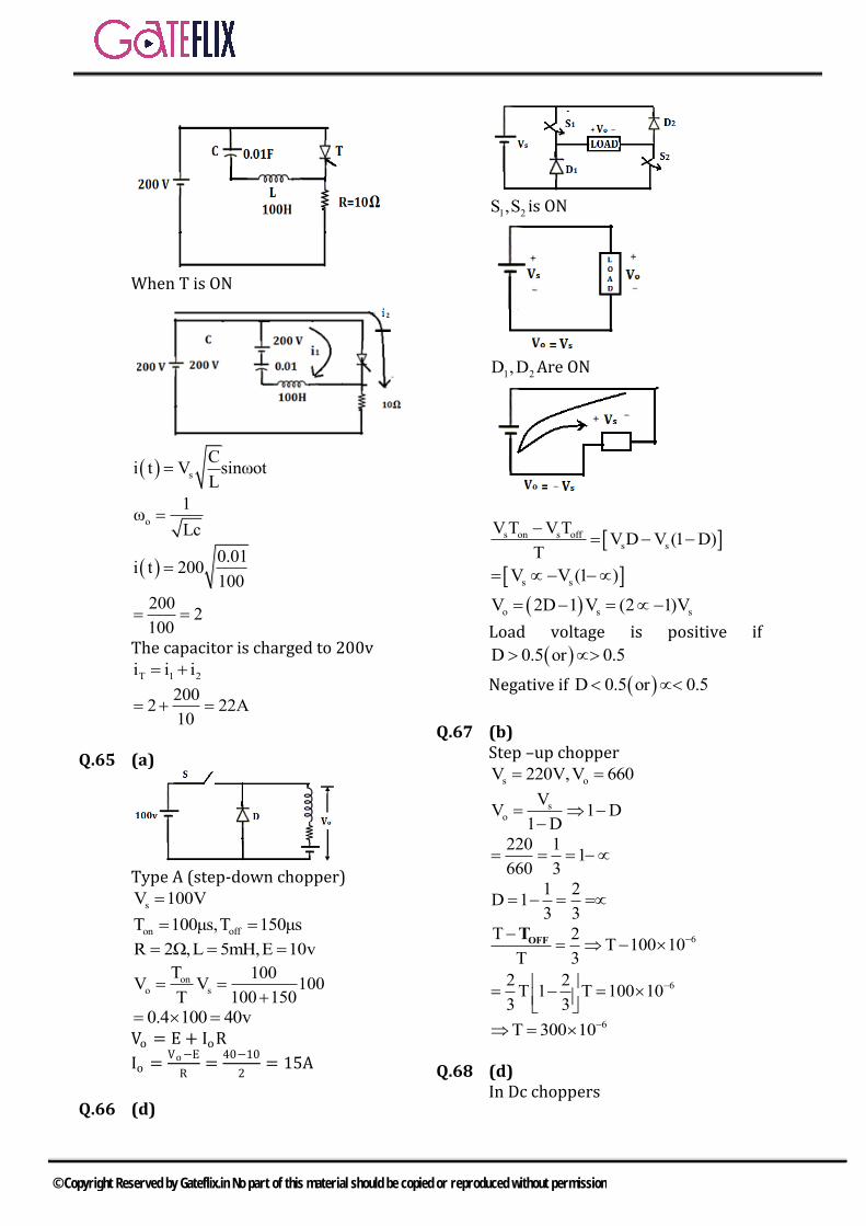
When T is ON
s
Ci t V sinωot
L
o
1ω
Lc
0.01
i t 200100
2002
100
The capacitor is charged to 200v
T 1 2i i i
2002 22A
10
Q.65 (a)
Type A (step-down chopper)
sV 100V
on offT 100μs,T 150μs
R 2Ω,L 5mH,E 10v
ono s
T 100V V 100
T 100 150
0.4 100 40v
Vo = E + IoR
Io =Vo−E
R=
40−10
2= 15A
Q.66 (d)
1 2S ,S is ON
1 2D ,D Are ON
s on s offs s
V T V TV D V (1 D)
T
s sV V (1 )
o s sV 2D 1 V (2 1)V
Load voltage is positive if
D 0.5 or 0.5
Negative if D 0.5 or 0.5
Q.67 (b) Step –up chopper
s oV 220V,V 660
so
VV 1 D
1 D
220 11
660 3
1 2D 1
3 3
6T 2T 100 10
T 3
OFFT
62 2T 1 T 100 10
3 3
6T 300 10
Q.68 (d) In Dc choppers
© Copyright Reserved by Gateflix.in No part of this material should be copied or reproduced without permission
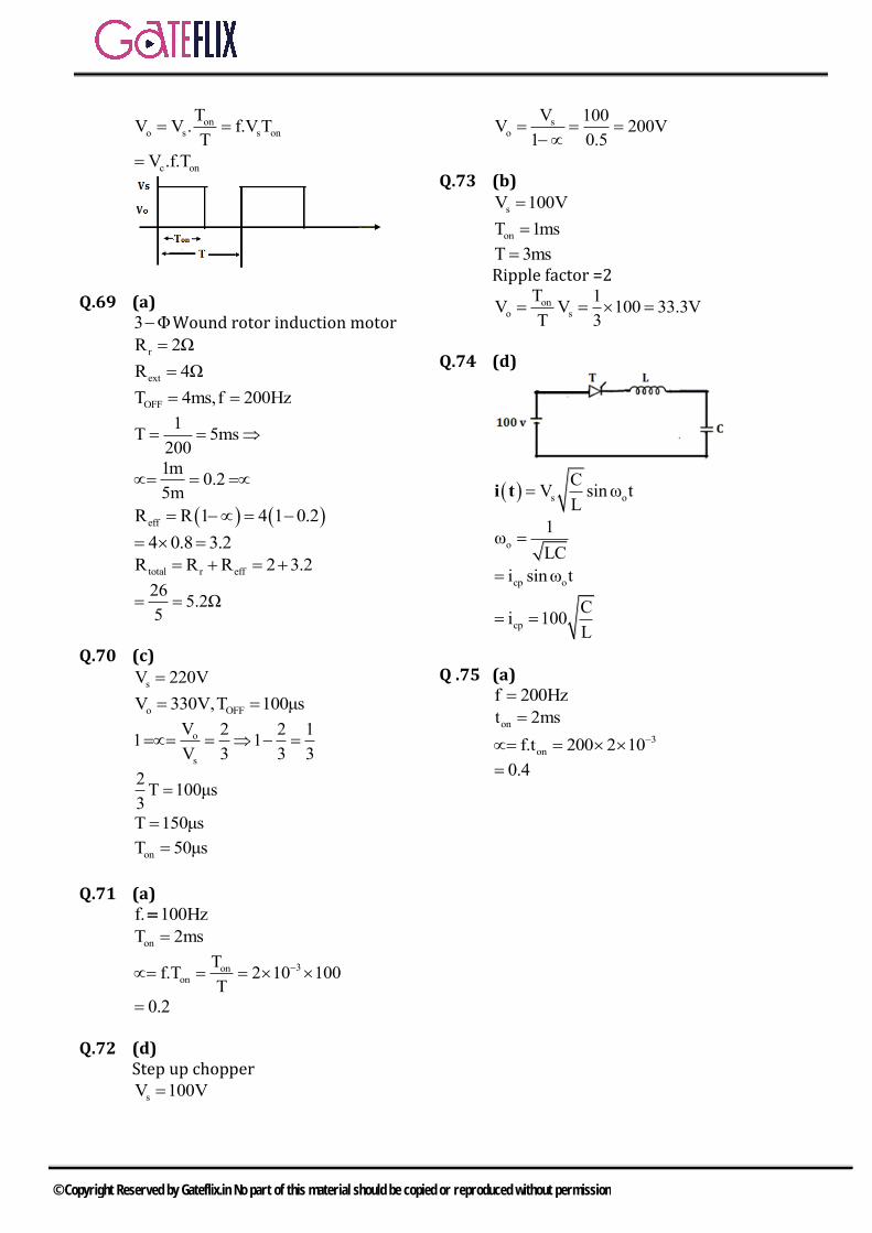
ono s s on
TV V . f.V T
T
c onV .f.T
Q.69 (a) 3 Φ Wound rotor induction motor
rR 2Ω
extR 4Ω
OFFT 4ms,f 200Hz
1T 5ms
200
1m0.2
5m
effR R 1 4 1 0.2
4 0.8 3.2
total r effR R R 2 3.2
265.2Ω
5
Q.70 (c)
sV 220V
o OFFV 330V,T 100μs
o
s
V 2 2 11 1
V 3 3 3
2T 100μs
3
T 150μs
onT 50μs
Q.71 (a) f. 100Hz
onT 2ms
3onon
Tf.T 2 10 100
T
0.2
Q.72 (d) Step up chopper
sV 100V
so
V 100V 200V
1 0.5
Q.73 (b)
sV 100V
onT 1ms
T 3ms
Ripple factor =2
ono s
T 1V V 100 33.3V
T 3
Q.74 (d)
s o
CV sin ω t
Li t
o
1ω
LC
cp oi sin ω t
cp
Ci 100
L
Q .75 (a) f 200Hz
ont 2ms3
onf.t 200 2 10
0.4
© Copyright Reserved by Gateflix.in No part of this material should be copied or reproduced without permission


