POWER ELECTRONICS Converters, Applications, and Design THIRD EDITION NED MOW Department of Electrical Engineering University of Minnesota Minneapolis, Minnesota TORE M. UNDELAND Department of Electrical Power Engineering Norwegian Uniuersity of Science and Technolom, NTNU Trondheim, Norway WILLIAM P. ROBBINS Department of Electrical Engineering University of Minnesota Minneapolis, Minnesota JOHN WILEY & SONS, INC. www.IranSwitching.ir
Transcript
POWER ELECTRONICS Converters, Applications, and Design THIRD EDITION
NED M O W Department of Electrical Engineering University of Minnesota Minneapolis, Minnesota
TORE M. UNDELAND Department of Electrical Power Engineering Norwegian Uniuersity of Science and Technolom, NTNU Trondheim, Norway
WILLIAM P. ROBBINS Department of Electrical Engineering University of Minnesota Minneapolis, Minnesota
JOHN WILEY & SONS, INC.
www.IranSwitching.ir
E!XECUIIVE EDROR Bill Zobrist SENIOR EDlTORIAL ASSISTANT Jovan Yglecias MARI<ETING MANAGER Katherine Hepburn SENIOR PRODUCSION EDlTOR Christine Cervoni SENIOR DESIGNER Kevin Murphy COVER DESIGNER David Levy
This book was set in limes Roman by The Clarinda Company and printed and bound by Hamilton Printing Company. The cover was printed by Brady Palmer Printing Company.
This book is printed on acid free paper.-
Copyright Q 2003 John Wiley & Sons, Inc. All rights reserved.
PSpice is a registered trademark of MicroSim Corporation. MATLAB is a registered trademark of The Mathworks, Inc,
No part of this publication may be reproduced, stored in a retrieval system or transmitted in any form or by any means, electronic, mechanical, photocopying, recording. scanning or otherwise, except as permitted under Sections 107 or 108 of the 1976 United States Copyright Act, without either the prior written permission of the Publisher, or authorization through payment of the appropriate. per-copy fee to the Copyright Clearance Center, 222 Rosewood Drive, Danvers, MA 01923, (978) 750-8400, fax (978) 750-4470. Requests to the Publisher for permission should be addressed to the Permissions Department, John Wdey & Sons, Inc., 11 1 River Street, Hoboken, NJ 07030, (201) 748-6011, fax (201) 748-
To order books or for customer service please call 1(800)225-5945. 6008, E-Mail: [email protected].
USA ISBN 978-0-471-22693-2
WIE ISBN 0-47 1-42908-2
Printed in the United States of America
20 19 18 17 16 15 14
www.IranSwitching.ir
PREFACE
MEDIA-ENHANCED THIRD EDITION
The first edition of this book was published in 1989 and the second edition in 1995. The basic intent of this edition, as in the two previous editions, is to provide a cohesive presen- tation of power electronics fundamentals for applications and design in the power range of 500 kW or less where a huge market exists and where the demand for power electronic en- gineers is likely to exist. This book has been adopted as a textbook at many universities around the world; it is for this reason that the text in this book has not been altered in any way. However, a CD-ROM has been added, which both the instructors and students will find very useful. This CD-ROM contains the following:
1. A large number of new problems with varying degrees of challenges have been added for homework assignments and self-learning.
2. PSpice-based simulation examples have been added to illustrate basic concepts and help in the design of converters. PSpiceB is an ideal simulation tool in power electron- ics education.
3. A newly developed magnetic component design program has been included. This program is extremely useful in showing design trade-offs; for example, influence of switching frequency on the size of inductors and transformers.
4. For all chapters in this book, Powerpoint-based slides are included and can be printed. These should be helpful to instructors in organizing their lectures and to students in taking notes in class on printed copies and for a quick review before examinations.
ORGANIZATION OF THE BOOK
This book is divided into seven parts. Part 1 presents an introduction to the field of power electronics, an overview of power
semiconductor switches, a review of pertinent electric and magnetic circuit concepts, and a generic discussion of the role of computer simulations in power electronics.
Part 2 discusses the generic converter topologies that are used in most applications. The actual semiconductor devices (transistors, diode, and so on) are assumed to be ideal, thus allowing us to focus on the converter topologies and their applications.
Part 3 discusses switch-mode dc and uninterruptible power supplies. Power supplies represent one of the major applications of power electronics.
Part 4 considers motor drives, which constitute another major applications area.
vii www.IranSwitching.ir
Part 5 includes several industrial and commercial applications in one chapter. Another chapter describes various high-power electric utility applications. The last chapter in this part of the book examines the harmonics and EMI concerns and remedies for interfacing power electronic systems with electric utilities.
Part 6 discusses the power semiconductor devices used in power electronic converters, including diodes, BJTs, MOSFETs, thyristors, GTOs, IGBTs, and MCTs.
Part 7 discusses the practical aspects of power electronic converter design, including snubber circuits, drive circuits, circuit layout, and heat sinks. An extensive new chapter on the design of high-frequency inductors and transformers has been added.
SOLUTIONS MANUAL
As with the former editions of this book, a Solutions Manual with completely worked-out solutions to all the problems (including those on the CD-ROM) is available to instructors. It can be requested from the Wiley web page: h t t p : / / w w w . w i l e y c o ~ c o l l e g ~ ~ ~ n .
ACKNOWLEDGMENTS
We wish to thank all the instructors who have allowed us this opportunity to write the third edition of our book by adopting its first and second editions. We express our sincere appre- ciation to the Wiley Executive Editor Bill Zobrist for his persistence in keeping us on schedule.
Ned Mohan Tore M. Undeland William I? Robbins
www.IranSwitching.ir
CONTENTS
PART 1 INTRODUCTION Chapter 1 Power Electronic Systems 1-1 Introduction 3 1-2 Power Electronics versus Linear Electronics 4 1-3 Scope and Applications 7 1-4 Classification of Power Processors and Converters 1-5 About the Text 12 1-6 Interdisciplinary Nature of Power Electronics 1-7 Convention of Symbols Used
9
13 14
Problems 14 References 15
Chapter 2 Overview of Power Semiconductor Switches 2-1 Introduction 16 2-2 Diodes 16 2-3 Thyristors 18 2-4 Desired Characteristics in Controllable Switches 20 2-5 Bipolar Junction Transistors and Monolithic Darlingtons 2-6 Metal-Oxide-Semiconductor Field Effect Transistors 2-7 Gate-Turn-Off Thyristors 26 2-8 Insulated Gate Bipolar Transistors 2-9 MOS-Controlled Thyristors 29 2-10 Comparison of Controllable Switches 2-1 1 Drive and Snubber Circuits 30 2- 12 Justification for Using Idealized Device Characteristics
24 25
27
29
3 1 Summary 32 Problems 32 References 32
1 3
16
Chapter 3 Review of Basic Electrical and Magnetic Circuit Concepts 3-1 Introduction 33 3-2 Electriccircuits 33 3-3 Magnetic Circuits 46
Sumnary 57 Problems 58 References 60
33
ix www.IranSwitching.ir
Chapter 4 Computer Simulation of Power Electronic Converters and Systems 61
4-1 Introduction 61 4-2 Challenges in Computer Simulation 4-3 Simulation Process 62 4-4 Mechanics of Simulation 64 4-5 Solution Techniques for Time-Domain Analysis 4-6 Widely Used, Circuit-Oriented Simulators 4-7 Equation Solvers 72
62
65 69
Summary 74 Problems 74 References 75
PART 2 GENERIC POWER ELECTRONIC CIRCUITS 77 Chapter 5 Line-Frequency Diode Rectifiers: Line-Frequency ac -+
Uncontrolled dc 79 5-1 Introduction 79 5-2 Basic Rectifier Concepts 80 5-3 Single-Phase Diode Bridge Rectifiers 5-4 Voltage-Doubler (Single-Phase) Rectifiers 100 5-5 Effect of Single-Phase Rectifiers on Neutral Currents in Three-Phase,
5-6 Three-Phase, Full-Bridge Rectifiers 103 5-7 Comparison of Single-Phase and Three-Phase Rectifiers 5-8 Inrush Current and Overvoltages at Turn-On 5-9 Concerns and Remedies for Line-Cumnt Harmonics and Low Power
Chapter 8 Switch-Mode dc-ac Inverters: dc t) Sinusoidal ac 200 8-1 Introduction 200 8-2 Basic Concepts of Switch-Mode Inverters 8-3 Single-Phase Inverters 21 1 8-4 Three-Phase Inverters 225 8-5 Effect of Blanking Time on Output Voltage in PWM Inverters 8-6 Other Inverter Switching Schemes 8-7 Rectifier Mode of Operation
PART 3 POWER SUPPLY APPLICATIONS Chapter 10 Switching dc Power Supplies 10-1 Introduction 301 10-2 Linear Power Supplies 301 10-3 Overview of Switching Power Supplies 10-4 dc-dc Converters with Electrical Isolation 10-5 Control of Switch-Mode dc Power Supplies 10-6 Power Supply Protection 341 10-7 Electrical Isolation in the Feedback Loop 10-8 Designing to Meet the Power Supply Specifications
302 304
322
344 346
Summary 349
299
301
www.IranSwitching.ir
xii CONTENTS
Problems 349 References 351
Chapter 11
11-1 Introduction 354 11-2 Power Line Disturbances 354 11-3 Power Conditioners 357 11-4 Unintermptible Power Supplies (UPSs)
Power Conditioners and Uninterruptible Power Supplies 354
358 Summary 363 Problems 363 References 364
PART 4 MOTOR DRIVE APPLICATIONS Chapter 12 Introduction to Motor Drives 12-1 Introduction 367 12-2 Criteria for Selecting Drive Components 368
summary 375 Problems 376 References 376
Chapter 13 dc Motor Drives 13-1 Introduction 377 13-2 Equivalent Circuit of dc Motors 13-3 Permanent-Magnet dc Motors 380 13-4 dc Motors with a Separately Excited Field Winding 13-5 Effect of Armature Current Waveform 13-6 dc Servo Drives 383 13-7 Adjustable-Speed dc Drives 391
Summary 396 Problems 396 References 398
377
381 382
Chapter 14 Induction Motor Drives 14-1 Introduction 399 14-2 Basic Principles of Induction Motor Operation 14-3 Induction Motor Characteristics at Rated (Line) Frequency
14-4 Speed Control by Varying Stator Frequency and Voltage 14-5 Impact of Nonsinusoidal Excitation on Induction Motors 14-6 Variable-Frequency Converter Classifications 14-7 Variable-Frequency PWM-VSI Drives 419 14-8 Variable-Frequency Square-Wave VSI Drives 14-9 Variable-Frequency CSI Drives 426 14-10 Comparison of Variable-Frequency Drives
400
and Rated Voltage 405 406 415
41 8
425
427
365 367
377
399
www.IranSwitching.ir
14-1 1 Line-Frequency Variable-Voltage Drives 14-12 Reduced Voltage Starting ("Soft Start") of Induction Motors 14-13 Speed Control by Static Slip Power Recovery
428 430
431 Summary 432 Problems 433 References 434
Chapter 15 Synchronous Motor Drives 15-1 Introduction 435 15-2 Basic Principles of Synchronous Motor Operation 15-3 Synchronous Servomotor Drives with Sinusoidal Waveforms 15-4 Synchronous Servomotor Drives with Trapezoidal Waveforms 15-5 Load-Commutated Inverter Drives 442 15-6 Cycloconverters 445
Problems 446 References 447
435 439
440
summary 445
PART 5 OTHER APPLICATIONS Chapter 16 Residential and Industrial Applications 16-1 Introduction 451 16-2 Residential Applications 451 16-3 Industrial Applications 455
summary 459 Problems 459 References 459
Chapter 17 Electric Utility Applications 17-1 Introduction 460 17-2 High-voltage dc Transmission 460 17-3 Static var Compensators 471 17-4 Interconnection of Renewable Energy Sources and Energy Storage
System to the Utility Grid 17-5 Active Filters 480
Summary 480 Problems 481 References 482
475
Chapter 18 Optimizing the Utility Interface with Power Electronic Systems
18-1 Introduction 483 18-2 Generation of Current Harmonics 18-3 Current Harmonics and Power Factor 18-4 Harmonic Standards and Recommended Practices 18-5 Need for Improved Utility Interface
Chapter 29 Component Temperature Control and Heat Sinks 29-1 Control of Semiconductor Device Temperatures 29-2 Heat Transfer by Conduction 29-3 Heatsinks 737 29-4 Heat Transfer by Radiation and Convection
Summary 742 Problems 743 References 743
730 73 1
739
Chapter 30 Design of Magnetic Components 30-1 Magnetic Materials and Cores 30-2 Copper Windings 752
74.4
667 669
696
730
744
www.IranSwitching.ir
CONTENTS xvii
30-3 Thermal Considerations 754 30-4 Analysis of a Specific Inductor Design 30-5 Inductor Design Procedures 760 30-6 Analysis of a Specific Transformer Design 30-7 Eddy Currents 771 30-8 Transformer Leakage Inductance 779 30-9 Transformer Design Procedure 780 30-10 Comparison of Transformer and Inductor Sizes
756
767
789 Summary 789 Problems 790 References 792
Index 793
www.IranSwitching.ir
PART 1
INTRODUCTION
www.IranSwitching.ir
CHAPTER 1
POWER ELECTRONIC SYSTEMS
1-1 INTRODUCTION
In broad terms, the task of power electronics is to process and control the flow of electric energy by supplying voltages and currents in a form that is optimally suited for user loads. Figure 1-1 shows a power electronic system in a block diagram form. The power input to this power processor is usually (but not always) from the electric utility at a line frequency of 60 or 50 Hz, single phase or three phases. The phase angle between the input voltage and the current depends on the topology and the control of the power processor. The processed output (voltage, current, frequency, and the number of phases) is as desired by the load. If the power processor's output can be regarded as a voltage source, the output current and the phase angle relationship between the output voltage and the current depend on the load characteristic. Normally, a feedback controller compares the output of the power processor unit with a desired (or a reference) value, and the error between the two is minimized by the controller. The power flow through such systems may be reversible, thus interchanging the roles of the input and the output.
In recent years, the field of power electronics has experienced a large growth due to confluence of several factors. The controller in the block diagram of Fig. 1-1 consists of linear integrated circuits and/or digital signal processors. Revolutionary advances in mi- croelectronics methods have led to the development of such controllers. Moreover, these advances in semiconductor fabrication technology have made it possible to significantly improve the voltage- and current-handling capabilities and the switching speeds of power semiconductor devices, which make up the power processor unit of Fig. 1-1. At the same time, the market for power electronics has significantly expanded. Electric utilities in the United States expect that by the year 2000 over 50% of the electrical load may be supplied through power electronic systems such as in Fig. 1-1. This growth in market may even be
Control Measurements
Figure 1-1 electronic system.
Block diagram of a power Controller Reference
3 www.IranSwitching.ir
4 CHAPTER 1 POWER ELECTRONIC SYSTEMS
higher in other parts of the world where the cost of energy is significantly higher than that in the United States. Various applications of power electronics are considered in Sec- tion 1-3.
1-2 POWER ELECTRONICS VERSUS LINEAR ELECTRONICS
In any power conversion process such as that shown by the block diagram in Fig. 1- 1, a small power loss and hence a high energy efficiency is important because of two reasons: the cost of the wasted energy and the difficulty in removing the heat generated due to dissipated energy. Other important considerations are reduction in size, weight, and cost.
The above objectives in most systems cannot be met by linear electronics where the semiconductor devices are operated in their linear (active) region and a line-frequency transformer is used for electrical isolation. As an example, consider the direct current (dc) power supply of Fig. 1-2a to provide a regulated output voltage V, to a load. The utility input may be typically at 120 or 240 V and the output voltage may be, for example, 5 V. The output is required to be electrically isolated from the utility input. In the linear power supply, a line-frequency transformer is used to provide electrical isolation and for step- ping down the line voltage. The rectifier converts the alternating current (ac) output of the transformer low-voltage winding into dc. The filter capacitor reduces the ripple in the dc voltage vd. Figure 1-21 shows the vd waveform, which depends on the utility voltage magnitude (normally in a t 10% range around its nominal value). The transformer turns
Line-frequency transformer
Utility
Rectifier Filter-capacitor
fa)
i
Rload
0 ' + t
Figure 1-2 Linenr dc power supply.
www.IranSwitching.ir
1-2 POWER ELECTRONICS VERSUS LINEAR ELECTRONICS 5
ratio must be chosen such that the minimum of the input voltage v, is greater than the desired output V,. For the range of the input voltage waveforms shown in Fig. 1-2b, the transistor is controlled to absorb the voltage difference between v, and V,, thus providing a regulated output. The transistor operates in its active region as an adjustable resistor, resulting in a low energy efficiency. The line-frequency transformer is relatively large and heavy.
In power electronics, the above voltage regulation and the electrical isolation are achieved, for example, by means of a circuit shown in Fig. 1-3a. In this system, the utility input is rectified into a dc voltage vd, without a line-frequency transformer. By operating the transistor as a switch (in a switch mode, either fully on or fully 08) at some high switching frequencyf,, for example at 300 kHz, the dc voltage vd is converted into an ac voltage at the switching frequency. This allows a high-frequency transformer to be used for stepping down the voltage and for providing the electrical isolation. In order to simplify this circuit for analysis, we will begin with the dc voltage vd as the dc input and omit the transformer, resulting in an equivalent circuit shown in Fig. 1-3b. Suffice it to
Power processor
I I
iL I I
c
I Controller Vo, ref
f b )
Figure 1-3 Switch-mode dc power supply.
www.IranSwitching.ir
6 CHAPTER 1 POWER ELECTRONIC SYSTEMS
say at this stage (this circuit is fully discussed in Chapters 7 and 10) that the transistor- diode combination can be represented by a hypothetical two-position switch shown in Fig. 1-4u (provided iL(t) > 0). The switch is in position u during the interval f, when the transistor is on and in position b when the transistor is off during toff. As a consequence, vOi equals V, and zero during ton and ton, respectively, as shown in Fig. 1-4b. Let us define
(1-1)
where Voi is the average (dc) value of vOi, and the instantaneous ripple voltage vfiPple(f), which has a zero average value, is shown in Fig. 1-4c. The L-C elements form a low-pass filter that reduces the ripple in the output voltage and passes the average of the input voltage, so that
where V, is the average output voltage. From the repetitive waveforms in Fig. 1-4b, it is easy to see that
voi(f) = Voi + v r i p p A 0
vo = v, ( 1-2)
1
( d )
Figure 1-4 Equivalent circuit, waveforms, and frequency spectrum of the supply in Fig. 1-3.
www.IranSwitching.ir
1-3 SCOPE AND APPLICATIONS 7
As the input voltage vd changes with time, Eq. 1-3 shows that it is possible to regulate V, at its desired value by controlling the ratio t,,/T,, which is called the duty ratio D of the transistor switch. Usually, T, (= l/fJ is kept constant and ton is adjusted.
There are several characteristics worth noting. Since the transistor operates as a switch, fully on or fully off, the power loss is minimized. Of course, there is an energy loss each time the transistor switches from one state to the other state through its active region (discussed in Chapter 2) . Therefore, the power loss due to switchings is linearly proportional to the switching frequency. This switching power loss is usually much lower than the power loss in linear regulated power supplies.
At high switching frequencies, the transformer and the filter components are very small in weight and size compared with line-frequency components. To elaborate on the role of high switching frequencies, the harmonic content in the waveform of v,; is obtained by means of Fourier analysis (see Problem 1-3 and its further discussion in Chapter 3) and plotted in Fig. 1-4d. It shows that vOi consists of an average (dc) value and of harmonic components that are at a multiple of the switching frequency f,. If the switching frequency is high, these ac components can be easily eliminated by a small filter to yield the desired dc voltage. The selection of the switching frequency is dictated by the compromise between the switching power dmipation in the transistor, which increases with the switching frequency, and the cost of the transformer and filter, which decreases with the switching frequency. As transistors with higher switching speeds become avail- able, the switching frequencies can be increased and the transformer and filter size reduced for the same switching power dissipation.
An important observation in the switch-mode circuit described above is that both the input and the output are dc, as in the linear regulated supply. The high switching fre- quencies are used to synthesize the output waveform, which in this example is dc. In many applications, the output is a low-frequency sine wave.
.3 SCOPE AND APPLICATIONS
The expanded market demand for power electronics has been due to several factors discussed below (see references 1 - 3 ) .
1. Switch-mode (dc) power supplies and uninterruptible power supplies. Advances in microelectronics fabrication technology have led to the development of com- puters, communication equipment, and consumer electronics, all of which require regulated dc power supplies and often uninterruptible power supplies.
2. Energy conservation. Increasing energy costs and the concern for the environ- ment have combined to make energy conservation a priority. One such application of power electronics is in operating fluorescent lamps at high frequencies (e.g., above 20 kHz) for higher efficiency. Another opportunity for large energy con- servation (see Problem 1-7) is in motor-driven pump and compressor systems [4]. In a conventional pump system shown in Fig. 1-5a, the pump operates at essen- tially a constant speed, and the pump flow rate is controlled by adjusting the position of the throttling valve. This procedure results in significant power loss across the valve at reduced flow rates where the power drawn from the utility remains essentially the same as at the full flow rate. This power loss is eliminated in the system of Fig. 1-56, where an adjustable-speed motor drive adjusts the pump speed to a level appropriate to deliver the desired flow rate. As will be discussed in Chapter 14 (in combination with Chapter 8), motor speeds can be adjusted very efficiently using power electronics. Load-proportional, capacity-
modulated heat pumps and air conditioners are examples of applying power elec- tronics to achieve energy conservation.
3 . Process control and factory automation. There is a growing demand for the enhanced performance offered by adjustable-speed-driven pumps and compres- sors in process control. Robots in automated factories are powered by electric servo (adjustable-speed and position) drives. It should be noted that the availabil- ity of process computers is a significant factor in making process control and factory automation feasible.
4. Transportation. In many countries, electric trains have been in widespread use for a long time. Now, there is also a possibility of using electric vehicles in large
TABLE 1-1 Power Electronic Applications
(a) Residential ( 4 Refrigeration and freezers Space heating Air conditioning Cooking Lighting Electronics (personal computers,
other entertainment equipment) (b) Commercial (el
Heating, ventilating, and air conditioning
Central refrigeration Lighting Computers and office equipment Uninterruptible power supplies
Transportation Traction control of electric vehicles Battery chargers for electric vehicles Electric locomotives Street cars, trolley buses Subways Automotive electronics including engine
controls Utility systems High-voltage dc transmission (HVDC) Static var compensation (SVC) Supplemental energy sources (wind,
photovoltaic), fuel cells Energy storage systems Induced-draft fans and boiler
feedwater pumps Aerospace Space shuttle power supply systems Satellite power systems Aircraft power systems Telecommunications Battery chargers Power supplies (dc and UPS)
www.IranSwitching.ir
1-4 CLASSIFICATION OF POWER PROCESSORS AND CONVERTERS 9
metropolitan areas to reduce smog and pollution. Electric vehicles would also require battery chargers that utilize power electronics.
5 . Electro-technical applications. These include equipment for welding, electroplat- ing, and induction heating.
6. Utility-related applications. One such application is in transmission of power over high-voltage dc (HVDC) lines. At the sending end of the transmission line, line-frequency voltages and currents are converted into dc. This dc is converted back into the line-frequency ac at the receiving end of the line. Power electronics is also beginning to play a significant role as electric utilities attempt to utilize the existing transmission network to a higher capacity [5 ] . Potentially, a large appli- cation is in the interconnection of photovoltaic and wind-electric systems to the utility grid.
Table 1-1 lists various applications that cover a wide power range from a few tens of watts to several hundreds of megawatts. As power semiconductor devices improve in perfor- mance and decline in cost, more systems will undoubtedly use power electronics.
1-4 CLASSIFICATION OF POWER PROCESSORS AND CONVERTERS
1-4-1 POWER PROCESSORS For a systematic study of power electronics, it is useful to categorize the power proces- sors, shown in the block diagram of Fig. 1-1, in terms of their input and output form or frequency. In most power electronic systems, the input is from the electric utility source. Depending on the application, the output to the load may have any of the following forms:
1. dc (a) regulated (constant) magnitude (b) adjustable magnitude
2. ac (a) constant frequency, adjustable magnitude (b) adjustable frequency and adjustable magnitude
The utility and the ac load, independent of each other, may be single phase or three phase. The power flow is generally from the utility input to the output load. There are exceptions, however. For example, in a photovoltaic system interfaced with the utility grid, the power flow is from the photovoltaics (a dc input source) to the ac utility (as the output load). In some systems the direction of power flow is reversible, depending on the operating conditions.
1-4-2 POWER CONVERTERS The power processors of Fig. 1-1 usually consist of more than one power conversion stage (as shown in Fig. 1-6) where the operation of these stages is decoupled on an instanta- neous basis by means of energy storage elements such as capacitors and inductors. Therefore, the instantaneous power input does not have to equal the instantaneous power output. We will refer to each power conversion stage as a converter. Thus, a converter is a basic module (building block) of power electronic systems. It utilizes power semicon-
www.IranSwitching.ir
10 CHAPTER 1 POWER ELECTRONIC SYSTEMS
Input - --{--H-+.r-t-- Converter 1 Energy Converter 2
storage element
output -
ductor devices controlled by signal electronics (integrated circuits) and possibly energy storage elements such as inductors and capacitors. Based on the form (frequency) on the two sides, converters can be divided into the following broad categories:
1. ac todc 2. dc to ac 3. dc to dc 4. ac to ac
We will use converter as a generic term to refer to a single power conversion stage that may perform any of the functions listed above. To be more specific, in ac-to-dc and dc-to-ac conversion, rectifier refers to a converter when the average power flow is from the ac to the dc side. Inverter refers to the converter when the average power flow is from the dc to the ac side. In fact, the power flow through the converter may be reversible. In that case, as shown in Fig. 1-7, we refer to that converter in terms of its rectifier and inverter modes of operation.
As an example, consider that the power processor of Fig. 1-6 represents the block diagram of an adjustable-speed ac motor drive (described in Chapter 14). As shown in Fig. 1-8, it consists of two converters: converter 1 operating as a rectifier that coriverts line-frequency ac into dc and converter 2 operating as an inverter that converts dc into adjustable-magnitude, adjustable-frequency ac. The flow of power in the normal (domi- nant) mode of operation is from the utility input source to the output motor load. During regenerative braking, the power flow reverses direction (from the motor to the utility), in which case converter 2 operates as a rectifier and converter 1 operates as an inverter. As mentioned earlier, an energy storage capacitor in the dc link between the two converters decouples the operation of the two converters on an instantaneous basis. Further insight can be gained by classifying converters according to how the devices within the converter are switched. There are three possibilities:
1 . Line frequency (naturally cornmutated) converters, where the utility line voltages present at one side of the converter facilitate the turn-off of the power semicon-
P
ac --I- Converter dc
- Rectifier mode
Inverter mode C--- P Figure 1-7 ac-to-dc converters.
www.IranSwitching.ir
1-4 CLASSIFICATION OF POWER PROCESSORS AND CONVERTERS 11
I I I - I
I
2.
3.
1-4-3
ductor devices. Similarly, the devices are turned on, phase locked to the line- voltage waveform. Therefore, the devices switch on and off at the line frequency of 50 or 60 Hz. Switching fjorced-commutated) converters, where the controllable switches in the converter are turned on and off at frequencies that are high compared to the line frequency. In spite of the high switching frequency internal to the converter, the converter output may be either dc or at a frequency comparable to the line frequency. As a side note in a switching converter, if the input appears as a voltage source, then the output must appear as a current source, or vice versa. Resonant and quasi-resonant converters, where the controllable switches turn on and/or turn off at zero voltage and/or zero current.
MATRIX CONVERTER AS A POWER PROCESSOR In the above two sections, we discussed that most practical power processors utilize more than one converter whose instantaneous operation is decoupled by an energy storage element (an inductor or a capacitor). Theoretically, it is possible to replace the multiple conversion stages and the intermediate energy storage element by a single power con- version stage called the matrix converter. Such a converter uses a matrix of semiconductor bidirectional switches, with a switch connected between each input terminal to each output terminal, as shown in Fig. 1-9a for an arbitrary number of input and output phases. With this general arrangement of switches, the power flow through the converter can reverse. Because of the absence of any energy storage element, the instantaneous power input must be equal to the power output, assuming idealized zero-loss switches. However, the phase angle between the voltages and currents at the input can be controlled and does not have to be the same as at the output (i.e., the reactive power input does not have to equal the reactive power output). Also, the form and the frequency at the two sides are independent, for example, the input may be three-phase ac and the output dc, or both may be dc, or both may be ac.
However, there are certain requirements on the switches and restrictions on the converter operation: If the inputs appear as voltage sources as shown in Fig. 1-9a, then the outputs must appear as current sources or vice versa. If both sides, for example, were to appear as voltage sources, the switching actions will inevitably connect voltage sources of unequal magnitude directly across each other; an unacceptable condition. The switch- ing functions in operating such a converter must ensure that the switches do not short- circuit the voltage sources and do not open-circuit the current sources. Otherwise, the converter will be destroyed.
www.IranSwitching.ir
12 CHAPTER 1 POWER ELECTRONIC SYSTEMS
Power processor
Utility source r _ _ _ _ _ _ _ _ _ _ _ _
I I
Voltage T - source
(a)
Figure 1-9 (Q) Matrix converter. (b) Voltage source.
Through a voltage source, the current can change instantaneously, whereas the volt- age across a current source can change instantaneously. If the input in Fig. 1-9u is a utility source, it is not an ideal voltage source due to its internal impedance corresponding to the transmission and distribution lines, transformers, etc., which are at the back of the utility outlet. To make it appear like a voltage source will require that we connect a small capacitance in parallel with it, as shown in Fig. 1-9b to overcome the effect of the internal impedance.
The switches in a matrix converter must be bidirectional, that is, they must be able to block voltages of either polarity and be able to conduct current in either direction. Such switches are not available and must be realized by a combination of the available unidi- rectional switches and diodes discussed in Chapter 2. There are also limits on the ratio of the magnitudes of the input and the output quantities.
In spite of numerous laboratory prototypes reported in research publications, the matrix converters so far have failed to show any significant advantage over conventional converters and hence have not found applications in practice. Therefore, we will not discuss them any further in this book.
1-5 ABOUT THE TEXT
The purpose of this book is to facilitate the study of practical and emerging power electronic converters made feasible by the new generation of power semiconductor de- vices. This book is divided into seven parts.
Part 1 of the book, which includes Chapter 1-4, presents an introduction, a brief review of basic concepts and devices, and computer simulations of power electronic systems. An overview of power semiconductor devices (discussed in detail in later parts of the book) and the justification for assuming them as ideal switches are presented in
www.IranSwitching.ir
1-6 INTERDISCIPLINARY NATURE OF POWER ELECTRONICS 13
Chapter 2. The basic electrical and magnetic concepts relevant to the discussion of power electronics are reviewed in Chapter 3. In Chapter 4, we briefly describe the role of computer simulations in the analysis and design of power electronic systems. Some of the simulation software packages suited for this purpose are also presented.
Part 2 (Chapters 5-9) describes power electronic converters in a generic manner. This way, the basic converter topologies used in more than one application can be described once, rather than repeating them each time a new application is encountered. This generic discussion is based on the assumption that the actual power semiconductor switches can be treated as ideal switches. Chapter 5 describes line-frequency diode rec- tifiers for ac-to-dc conversion. The ac-to-dc conversion using line-commutated (naturally commutated) thyristor converters operating in the rectifier and the inverter mode is dis- cussed in Chapter 6. Switching converters for dc to dc, and dc to sinusoidal ac using controlled switches are described in Chapters 7 and 8, respectively. The discussion of resonant converters in a generic manner is presented in Chapter 9.
We decided to discuss ac-to-ac converters in the application-based chapters due to their application-specific nature. The matrix converters, which in principle can be ac-to-ac converters, were briefly described in Section 1-4-3. The static transfer switches are discussed in conjunction with the unintermptible power supplies in Section 11-4-4. Con- verters where only the voltage magnitude needs to be controlled without any change in ac frequency are described in Section 14-12 for speed control of induction motors and in Section 17-3 for static var compensators (thyristor-controlled inductors and thyristor- switched capacitors). Cycloconverters for very large synchronous-motor drives are dis- cussed in Section 15-6. High-frequency-link integral-half-cycle converters are discussed in Section 9-8. Integral-half-cycle controllers supplied by line-frequency voltages for heating-type applications are discussed in Section 16-3-3.
Part 3 (Chapters 10 and 11) deals with power supplies: switching dc power supplies (Chapter 10) and unintermptible ac power supplies (Chapter 11). Part 4 describes motor drive applications in Chapters 12- 15.
Other applications of power electronics are covered in Part 5 , which includes resi- dential and industrial applications (Chapter 16), electric utility applications (Chapter 17), and the utility interface of power electronic systems (Chapter 18).
Part 6 (Chapters 19-26) contains a qualitative description of the physical operating principles of semiconductor devices used as switches. Finally, Part 7 (Chapters 27-30) presents the practical design considerations of power electronic systems, including pro- tection and gate-drive circuits, thermal management, and the design of magnetic compo- nents.
The reader is also urged to read the overview of the textbook presented in the Preface.
1-6 INTERDISCIPLINARY NATURE OF POWER ELECTRONICS
The discussion in this introductory chapter shows that the study of power electronics encompasses many fields within electrical engineering, as illustrated by Fig. 1- 10. These include power systems, solid-state electronics, electrical machines, analog/digital control and signal processing, electromagnetic field calculations, and so on. Combining the knowledge of these diverse fields makes the study of power electronics challenging as well as interesting. There are many potential advances in all these fields that will improve the prospects for applying power electronics to new applications.
www.IranSwitching.ir
14 CHAPTER 1 POWER ELECTRONIC SYSTEMS
b y s t e r n 9
Figure 1-10 Interdisciplinary nature of power electronics.
1-? CONVENTION OF SYMBOLS USED
In this textbook, for instantaneous values of variables such as voltage, current, and power that are functions of time, the symbols used are lowercase letters v, i, andp, respectively. We may or may not explicitly show that they are functions of time, for example, using v rather than v(t) . The uppercase symbols V and I refer to their values computed from their instantaneous waveforms. They generally refer to an average value in dc quantities and a root-mean-square (rms) value in ac quantities. If there is a possibility of confusion, the subscript avg or rms is added explicitly. The peak values are always indicated by the symbol ''" " on top of the uppercase letters. The average power is always indicated by P.
PROBLEMS
1 - 1 In the power processor of Fig. 1 - 1, the energy efficiency is 95%. The output to the three-phase load is as follows: 200 V line-to-liine (rms) sinusoidal voltages at 52 Hz and line current of 10 A at a power factor of 0.8 (lagging). The input to the power processor is a single-phase utility voltage of 230 V at 60 Hz. The input power is drawn at a unity power factor. Calculate the input current and the input power.
1-2 Consider a linear regulated dc power supply (Fig. 1-2a). The instantaneous input voltage corre- sponds to the lowest waveform in Fig. 1-26, where V,,,, = 20 V and Vd,- = 30 V. Approximate this waveform by a triangular wave consisting of two linear segments between the above two values. Let V, = 15 V and assume that the output load is constant. Calculate the energy efficiency in this part of the power supply due to losses in the transistor.
1-3 Consider a switch-mode dc power supply represented by the circuit in Fig. 1 4 1 . The input dc voltage V, = 20 V and the switch duty ratio D = 0.75. Calculate the Fourier components of voi using the description of Fourier analysis in Chapter 3.
1-4 In Problem 1-3, the switching frequencyf, = 300 kHz and the resistive load draws 240 W. The filter components corresponding to Fig. 141 are L = 1.3 pH and C = 50 pF. Calculate the attenuation in decibels of the ripple voltage in v, at various harmonic frequencies. (Hint: To calculate the load resistance, assume the output voltage to be a constant dc without any ripple.)
1-5 In Problem 1 - 4 , assume the output voltage to be a pure dc V, = 15 V. Calculate and draw the voltage and current associated with the filter inductor L, and the current through C. Using the capacitor current obtained above, estimate the peak-to-peak ripple in the voltage across C, which was initially assumed to be zero. (Hint: Note that under steady-state conditions, the average value of the current through C is zero.)
www.IranSwitching.ir
REFERENCES 15
1-6 Considering only the switching frequency component in voi in Problems 1-3 and 1-4, calculate the peak-to-peak ripple in the output voltage across C . Compare the result with that obtained in Problem 1-5.
1-7 Reference 4 refers to a U.S. Department of Energy report that estimated that over 100 billion kWh/year can be saved in the United States by various energy conservation techniques applied to the pump-driven systems. Calculate (a) how many 1OOO-MW generating plants running constantly supply this wasted energy, which could be saved, and (b) the savings in dollars if the cost of electricity is 0.1 $/kWh.
REFERENCES
1.
2.
B. K. Bose, “Power Electronics-A Technology Review,” Proceedings of the IEEE, Vol.
E. Ohno, “The Semiconductor Evolution in Japan-A Four Decade Long Maturity Thriving to an Indispensable Social Standing,” Proceedings of the International Power Electronics Conference (Tokyo), 1990, Vol. 1, pp. 1 - 10.
3. M. Nishihara, “Power Electronics Diversity,” Proceedings of the International Power Elec- tronics Conference (Tokyo), 1990, Vol. 1 , pp. 21-28.
4. N. Mohan and R. J. Ferraro, “Techniques for Energy Conservation in AC Motor Driven Systems,” Electric Power Research Institute Final Report EM-2037, Project 1201-1213, S e p tember 1981. N. G. Hingorani, “Flexible ac Transmission,” IEEE Spectrum, April 1993, pp. 40-45. N. Mohan, “Power Electronic Circuits: An Overview,” IEEEIIECON Conference Proceed- ings, 1988, Vol. 3, pp. 522-521.
80, NO. 8, August 1992, pp. 1303- 1334.
5 . 6 .
www.IranSwitching.ir
CHAPTER 2
OVERVIEW OF POWER SEMICONDUCTOR SWITCHES
2-1 INTRODUCTION
The increased power capabilities, ease of control, and reduced costs of modem power semiconductor devices compared to those of just a few years ago have made converters affordable in a large number of applications and have opened up a host of new converter topologies for power electronic applications. In order to clearly understand the feasibility of these new topologies and applications, it is essential that the characteristics of available power devices be put in perspective. To do this, a brief summary of the terminal char- acteristics and the voltage, current, and switching speed capabilities of currently available power devices are presented in this chapter.
If the power semiconductor devices can be considered as ideal switches, the analysis of converter topologies becomes much easier. This approach has the advantage that the details of device operation will not obscure the basic operation of the circuit. Therefore, the important converter characteristics can be more clearly understood. The summary of device characteristics will enable us to determine how much the device characteristics can be idealized.
Presently available power semiconductor devices can be classified into three groups according to their degree of controllability:
1. Diodes. On and off states controlled by the power circuit. 2. Thyristors. Latched on by a control signal but must be turned off by the power
3 . Controllable switches. Turned on and off by control signals. circuit.
The controllable switch category includes several device types including bipolar junction transistors (BJTs), metal-oxide- semiconductor field effect transistors (MOSFETs), gate turn off (GTO) thyristors, and insulated gate bipolar transistors (IGBTs). There have been major advances in recent years in this category of devices.
2-2 DIODES
Figures 2-la and 2-lb show the circuit symbol for the diode and its steady-state i-v characteristic. When the diode is forward biased, it begins to conduct with only a small
forward voltage across it, which is on the order of 1 V. When the diode is reverse biased, only a negligibly small leakage current flows through the device until the reverse break- down voltage is reached. In normal operation, the reverse-bias voltage should not reach the breakdown rating.
In view of a very small leakage current in the blocking (reverse-bias) state and a small voltage in the conducting (forward-bias) state, as compared to the operating voltages and currents of the circuit in which the diode is used, the i-v characteristic for the diode can be idealized, as shown in Fig. 2-lc. This idealized characteristic can be used for analyzing the converter topology but should not be used for the actual converter design, when, for example, heat sink requirements for the device are being estimated.
At turn-on, the diode can be considered an ideal switch because it turns on rapidly compared to the transients in the power circuit. However, at turn-off, the diode current reverses for a reverse-recovery time tr,, as is indicated in Fig. 2-2, before falling to zero. This reverse-recovery (negative) current is required to sweep out the excess carriers in the diode and allow it to block a negative polarity voltage. The reverse-recovery current can lead to overvoltages in inductive circuits. In most circuits, this reverse current does not affect the converter input/output characteristic and so the diode can also be considered as ideal during the turn-off transient.
Depending on the application requirements, various types of diodes are available:
1. Schottky diodes. These diodes are used where a low forward voltage drop (typ- ically 0.3 V) is needed in very low output voltage circuits. These diodes are limited in their blocking voltage capabilities to 50- 100 V.
2. Fast-recovery diodes. These are designed to be used in high-frequency circuits in combination with controllable switches where a small reverse-recovery time is needed. At power levels of several hundred volts and several hundred amperes, such diodes have trr ratings of less than a few microseconds.
3. Linelfrequency diodes. The on-state voltage of these diodes is designed to be as low as possible and as a consequence have larger t,,, which are acceptable for
Figure 2-2 Diode turn-off.
www.IranSwitching.ir
18 CHAPTER 2 OVERVIEW OF POWER SEMICONDUCTOR SWITCHES
f 0
line-frequency applications. These diodes are available with blocking voltage ratings of several kilovolts and current ratings of several kiloamperes. Moreover, they can be connected in series and parallel to satisfy any voltage and current requirement.
,On-state
* U~~ 2
2-3 THYRISTORS
The circuit symbol for the thyristor and its i-v characteristic are shown in Figs. 2-3a and 2-3b. The main current flows from the anode (A) to the cathode (K). In its off-state, the thyristor can block a forward polarity voltage and not conduct, as is shown in Fig. 2-3b by the off-state portion of the i-v characteristic.
The thyristor can be triggered into the on state by applying a pulse of positive gate current for a short duration provided that the device is in its forward-blocking state. The resulting i-v relationship is shown by the on-state portion of the characteristics shown in Fig. 2-3b. The forward voltage drop in the on state is only a few volts (typically 1-3 V depending on the device blocking voltage rating).
Once the device begins to conduct, it is latched on and the gate current can be removed. The thyristor cannot be turned off by the gate, and the thyristor conducts as a diode. Only when the anode current tries to go negative, under the influence of the circuit in which the thyristor is connected, does the thyristor turn off and the current go to zero. This allows the gate to regain control in order to turn the device on at some controllable time after it has again entered the forward-blocking state.
In reverse bias at voltages below the reverse breakdown voltage, only a negligibly small leakage current flows in the thyristor, as is shown in Fig. 2-3b. Usually the thyristor voltage ratings for forward- and reverse-blocking voltages are the same. The thyristor current ratings are specified in terms of maximum rms and average currents that it is capable of conducting.
Using the same arguments as for diodes, the thyristor can be represented by the idealized characteristics shown in Fig. 2-3c in analyzing converter topologies.
In an application such as the simple circuit shown in Fig. 2-4u, control can be exercised over the instant of current conduction during the positive half cycle of source voltage. When the thyristor current tries to reverse itself when the source voltage goes negative, the idealized thyristor would have its current become zero immediately after r = f iT , as is shown in the waveform in Fig. 2-4b.
However, as specified in the thyristor data sheets and illustrated by the waveforms in Fig. 2-4c, the thyristor current reverses itself before becoming zero. The important pa- rameter is not the time it takes for the current to become zero from its negative value, but rather the turn-off time interval fq defined in Fig. 2-4c from the zero crossover of the current to the zero crossover of the voltage across the thyristor. During rq a reverse voltage must be maintained across the thyristor, and only after this time is the device capable of blocking a forward voltage without going into its on state. If a forward voltage is applied to the thyristor before this interval has passed, the device may prematurely turn on, and damage to the device and/or circuit could result. Thyristor data sheets specify fq with a specified reverse voltage applied during this interval as well as a specified rate of rise of voltage beyond this interval. This interval rq is sometimes called the circuit-commutated recovery time of the thyristor.
Depending on the application requirements, various types of thyristors are available. In addition to voltage and current ratings, turn-off time fq, and the forward voltage drop,
20 CHAPTER 2 OVERVIEW OF POWER SEMICONDUCTOR SWITCHES
other characteristics that must be considered include the rate of rise of the current (dildt) at turn-on and the rate of rise of voltage (dvldt) at turn-off.
1. Phase-control thyristors. Sometimes termed converter thyristors, these are used primarily for rectifying line-frequency voltages and currents in applications such as phase-controlled rectifiers for dc and ac motor drives and in high-voltage dc power transmission. The main device requirements are large voltage and current- handling capabilities and a low on-state voltage drop. This type of thyristor has been produced in wafer diameters of up to 10 cm, where the average current is about 4OOO A with blocking voltages of 5-7 kV. On-state voltages range from 1.5 V for 1OOO-V devices to 3.0 V for the 5-7-kV devices.
2. Inverter-grade thyristors. These are designed to have small turn-off times tq in addition to low on-state voltages, although on-state voltages are larger in devices with shorter values of tq. These devices are available with ratings up to 2500 V and 1500 A. Their turn-off times are usually in the range of a few microseconds to 100 ps depending on their blocking voltage ratings and on-state voltage drops.
3. Light-activated thyristors. These can be triggered on by a pulse of light guided by optical fibers to a special sensitive region of the thyristor. The light-activated triggering of the thyristor uses the ability of light of appropriate wavelengths to generate excess electron-hole pairs in the silicon. The primary use of these thyristors are in high-voltage applications such as high-voltage dc transmission where many thyristors are connected in series to make up a converter valve. The differing high potentials that each device sees with respect to ground poses sig- nificant difficulties in providing triggering pulses. Light-activated thyristors have been reported with ratings of 4 kV and 3 kA, on-state voltages of about 2 V, and light trigger power requirements of 5 mW.
Other variations of these thyristors are gate-assisted turn-off thyristors (GATTs), asymmetrical silicon-controlled rectifiers (ASCRs), and reverse-conducting thyristors (RCTs). These are utilized based on the application.
2-4 DESIRED CHARACTERISTICS IN CONTROLLABLE SWITCHES
As mentioned in the introduction, several types of semiconductor power devices including BJTs, MOSFETs, GTOs, and IGBTs can be turned on and off by control signals applied to the control terminal of the device. These devices we term controllable switches and are represented in a generic manner by the circuit symbol shown in Fig. 2-5. No current flows when the switch is off, and when it is on, current can flow in the direction of the arrow only. The ideal controllable switch has the following characteristics:
1. Block arbitrarily large forward and reverse voltages with zero current flow when
2. Conduct arbitrarily large currents with zero voltage drop when on. Off.
Y+ "T
- I Figure 2-5 Generic controllable switch.
www.IranSwitching.ir
2-4 DESIRED CHARACTERISTICS IN CONTROLLABLE SWITCHES 21
3. Switch from on to off or vice versa instantaneously when triggered. 4. Vanishingly small power required from control source to trigger the switch.
Real devices, as we intuitively expect, do not have these ideal characteristics and hence will dissipate power when they are used in the numerous applications already mentioned. If they dissipate too much power, the devices can fail and, in doing so, not only will destroy themselves but also may damage the other system components.
Power dissipation in semiconductor power devices is fairly generic in nature; that is, the same basic factors governing power dissipation apply to all devices in the same manner. The converter designer must understand what these factors are and how to minimize the power dissipation in the devices.
In order to consider power dissipation in a semiconductor device, a controllable switch is connected in the simple circuit shown in Fig. 2-6a. This circuit models a very commonly encountered situation in power electronics; the current flowing through a
22 CHAPTER 2 OVERVIEW OF POWER SEMICONDUCTOR SWITCHES
switch also must flow through some series inductance(s). This circuit is similar to the circuit of Fig. 1-3b, which was used to introduce switch-mode power electronic circuits. The dc current source approximates the current that would actually flow due to inductive energy storage. The diode is assumed to be ideal because our focus is on the switch characteristics, though in practice the diode reverse-recovery current can significantly affect the stresses on the switch.
When the switch is on, the entire current I , flows through the switch and the diode is reverse biased. When the switch is turned off, I , flows through the diode and a voltage equal to the input voltage v d appears across the switch, assuming a zero voltage drop across the ideal diode. Figure 2-6b shows the waveforms for the current through the switch and the voltage across the switch when it is being operated at a repetition rate or switching frequency off, = UT,, with T, being the switching time period. The switching waveforms are represented by linear approximations to the actual waveforms in order to simplify the discussion.
When the switch has been off for a while, it is turned on by applying a positive control signal to the switch, as is shown in Fig. 2-66. During the turn-on transition of this generic switch, the current buildup consists of a short delay time td(on) followed by the current rise time tri. Only after the current I, flows entirely through the switch can the diode become reverse biased and the switch voltage fall to a small on-state value of Von with a voltage fall time of 9". The waveforms in Fig. 2-6b indicate that large values of switch voltage and current are present simultaneously during the turn-on crossover inter- val tc(on), where
The energy dissipated in the device during this turn-on transition can be approximated from Fig. 2-6c as
where it is recognized that no energy dissipation occurs during the turn-on delay interval
Once the switch is fully on, the on-state voltage Von will be on the order of a volt or so depending on the device, and it will be conducting a current I,. The switch remains in conduction during the on interval ton, which in general is much larger than the turn-on and turn-off transition times. The energy dissipation Won in the switch during this on-state interval can be approximated as
td(on).
where ton > tc(on)r tc (of0 . In order to turn the switch off, a negative control signal is applied to the control
terminal of the switch. During the turn-off transition period of the generic switch, the voltage build-up consists of a turn-off delay time td(off) and a voltage rise time tN. Once the voltage reaches its final value of v d (see Fig. 2-64 , the diode can become forward biased and begin to conduct current. The current in the switch falls to zero with a current fall time tri as the current I , cornmutates from the switch to the diode. Large values of switch voltage and switch current occur simultaneously during the crossover interval t,(,fO, where
(2-4)
The energy dissipated in the switch during this turn-off transition can be written, using Fig. 2-6c, as
tc(of0 = t rv + t f i
www.IranSwitching.ir
2-4 DESIRED CHARACTERISTICS IN CONTKOLLABLE SWITCHES 23
where any energy dissipation during the turn-off delay interval td(off) is ignored since it is small compared to Wc(off).
The instantaneous power dissipation pT( t ) = v,i, plotted in Fig. 2-6c makes it clear that a large instantaneous power dissipation occurs in the switch during the turn-on and turn-off intervals. There are!, such turn-on and turn-off transitions per second. Hence the average switching power loss P, in the switch due to these transitions can be approximated from Eqs. 2-2 and 2-5 as
Ps= ?'2VJo!Xtc(on)+ tc(off9 (2-6)
This is an important result because it shows that the switching power loss in a semicon- ductor switch varies linearly with the switching frequency and the switching times. Therefore, if devices with short switching times are available, it is possible to operate at high switching frequencies in order to reduce filtering requirements and at the same time keep the switching power loss in the device from being excessive.
The other major contribution to the power loss in the switch is the average power dissipated during the on-state Po,, which varies in proportion to the on-state voltage. From Eq. 2-3, Po, is given by
(2-7) ton P, = v I -
On O T ,
which shows that the on-stage voltage in a switch should be as small as possible. The leakage current during the off state (switch open) of controllable switches is
negligibly small, and therefore the power loss during the off state can be neglected in practice. Therefore, the total average power dissipation P, in a switch equals the sum of P, and Po,.
Form the considerations discussed in the preceding paragraphs, the following char- acteristics in a controllable switch are desirable:
1 . 2. 3.
4.
5 .
6.
7.
8.
Small leakage current in the off state. Small on-state voltage Von to minimize on-state power losses. Short turn-on and turn-off times. This will permit the device to be used at high switching frequencies. Large forward- and reverse-voltage-blocking capability. This will minimize the need for series connection of several devices, which complicates the control and protection of the switches. Moreover, most of the device types have a minimum on-state voltage regardless of their blocking voltage rating. A series connection of several such devices would lead to a higher total on-state voltage and hence higher conduction losses. In most (but not all) converter circuits, a diode is placed across the controllable switch to allow the current to flow in the reverse direction. In those circuits, controllable switches are not required to have any significant re- verse-voltage-blocking capability. High on-state current rating. In high-current applications, this would minimize the need to connect several devices in parallel, thereby avoiding the problem of current sharing. Positive temperature coefficient of on-state resistance. This ensures that paralleled devices will share the total current equally. Small control power required to switch the device. This will simplify the control circuit design. Capability to withstand rated voltage and rated current simultaneously while switching. This will eliminate the need for external protection (snubber) circuits across the device.
www.IranSwitching.ir
24 CHAPTER 2 OVERVIEW OF POWER SEMICONDUCTOR SWITCHES
2
9. Large dvldr and dildt ratings. This will minimize the need for external circuits otherwise needed to limit dvldt and dildt in the device so that it is not damaged.
We should note that the clamped-inductive-switching circuit of Fig. 2-6a results in higher switching power loss and puts higher stresses on the switch in comparison to the resistive-switching circuit shown in Problem 2-2 (Fig. P2-2).
We now will briefly consider the steady-state i-v characteristics and switching times of the commonly used semiconductor power devices that can be used as controllable switches. As mentioned previously, these devices include BJTs, MOSFETs, GTOs, and IGBTs. The details of the physical operation of these devices, their detailed switching characteristics, commonly used drive circuits, and needed snubber circuits are discussed in Chapters 19-28.
.5 BIPOLAR JUNCTION TRANSISTORS AND MONOLITHIC DARLINGTONS
The circuit symbol for an NPN BJT is shown in Fig. 2-7a, and its steady-state i-v characteristics are shown in Fig. 2-7b. As shown in the i-v characteristics, a sufficiently large base current (dependent on the collector current) results in the device being fully on. This requires that the control circuit provide a base current that is sufficiently large so that
l C I, > - ~ F E
where hFE is the dc current gain of the device. The on-state voltage VCE(sat) of the power transistors is usually in the 1-2-V range,
so that the conduction power loss in the BJT is quite small. The idealized t v character- istics of the BJT operating as a switch are shown in Fig. 2-7c.
Bipolar junction transistors are current-controlled devices, and base current must be supplied continuously to keep them in the on state. The dc current gain hFE is usually only 5-10 in high-power transistors, and so these devices are sometimes connected in a Darlington or triple Darlington configuration, as is shown in Fig. 2-8, to achieve a larger current gain. Some disadvantages accrue in this configuration including slightly higher overall VCE(sat) values and slower switching speeds.
Whether in single units or made as a Darlington configuration on a single chip [a monolithic Darlington (MD)] , BJTs have significant storage time during the turn-off transition. Typical switching times are in the range of a few hundred nanoseconds to a few microseconds.
2-6 METAL- OXIDE-SEMICONDUCTOR FIELD EFFECT TRANSISTORS 25
'BE -
- O E
-
Including MDs, BJTs are available in voltage ratings up to 1400 V and current ratings of a few hundred amperes. In spite of a negative temperature coefficient of on-state resistance, modern BJTs fabricated with good quality control can be paralleled provided that care is taken in the circuit layout and that some extra current margin is provided, that is, where theoretically four transistors in parallel would suffice based on equal current sharing, five may be used to tolerate a slight current imbalance.
2-6 METAL- OXIDE- SEMICONDUCTOR FIELD EFFECT TRANSISTORS
The circuit symbol of an n-channel MOSFET is shown in Fig. 2-9a. It is a voltage- controlled device, as is indicated by the C v characteristics shown in Fig. 2-9b. The device is fully on and approximates a closed switch when the gate-source voltage is below the threshold value, VGS(*). The idealized characteristics of the device operating as a switch are shown in Fig. 2-9c.
Metal- oxide- semiconductor field effect transistors require the continuous applica- tion of a gate-source voltage of appropriate magnitude in order to be in the on state. No gate current flows except during the transitions from on to off or vice versa when the gate capacitance is being charged or discharged. The switching times are very short, being in
26 CHAPTER 2 OVERVIEW OF POWER SEMICONDUCTOR SWITCHES
the range of a few tens of nanoseconds to a few hundred nanoseconds depending on the device type.
The on-state resistance rDSfon) of the MOSFET between the drain and source increases rapidly with the device blocking voltage rating. On a per-unit area basis, the on-state resistance as a function of blocking voltage rating BVD, can be expressed as
(2-9) 2.5-2.7 rDS(on) = k BVDSS
where k is a constant that depends on the device geometry. Because of this, only devices with small voltage ratings are available that have low on-state resistance and hence small conduction losses.
However, because of their fast switching speed, the switching losses can be small in accordance with Eiq. 2-6. From a total power loss standpoint, 300-400-V MOSFETs compete with bipolar transistors only if the switching frequency is in excess of 30- 100 kHz. However, no definite statement can be made about the crossover frequency because it depends on the operating voltages, with low voltages favoring the MOSFET.
Metal- oxide- semiconductor field effect transistors are available in voltage ratings in excess of lo00 V but with small current ratings and with up to 100 A at small voltage ratings. The maximum gate-source voltage is 220 V, although MOSFETs that can be controlled by 5-V signals are available.
Because their on-state resistance has a positive temperature coefficient, MOSFETs are easily paralleled. This causes the device conducting the higher current to heat up and thus forces it to equitably share its current with the other MOSFETs in parallel.
2-7 GATE-TURN-OFF THYRISTORS
The circuit symbol for the GTO is shown in Fig. 2-1% and its steady-state t v charac- teristic is shown in Fig. 2-lob.
Like the thyristor, the GTO can be turned on by a short-duration gate current pulse, and once in the on-state, the GTO may stay on without any further gate current. However, unlike the thyristor, the GTO can be turned off by applying a negative gate-cathode voltage, therefore causing a sufficiently large negative gate current to flow. This negative gate current need only flow for a few microseconds (during the turn-off time), but it must have a very large magnitude, typically as large as one-third the anode current being turned off. The GTOs can block negative voltages whose magnitude depends on the details of the
GTO design. Idealized characteristics of the device operating as a switch are shown in Fig. 2-1Oc.
Even though the GTO is a controllable switch in the same category as MOSFETs and BJTs, its turn-off switching transient is different from that shown in Fig. 2-6b. This is because presently available GTOs cannot be used for inductive turn-off such as is illus- trated in Fig. 2-6 unless a snubber circuit is connected across the GTO (see Fig. 2-lla). This is a consequence of the fact that a large dvldt that accompanies inductive turn-off cannot be tolerated by present-day GTOs. Therefore a circuit to reduce dvldt at turn-off that consists of R, C, and D, as shown in Fig. 2-lla, must be used across the GTO. The resulting waveforms are shown in Fig. 2-llb, where dvldt is significantly reduced com- pared to the dvldt that would result without the turn-off snubber circuit. The details of designing a snubber circuit to shape the switching waveforms of GTOs are discussed in Chapter 27.
The on-state voltage (2-3 V) of a GTO is slightly higher than those of thyristors. The GTO switching speeds are in the range of a few microseconds to 25 FS. Because of their capability to handle large voltages (up to 4.5 kV) and large currents (up to a few kilo- amperes), the GTO is used when a switch is needed for high voltages and large currents in a switching frequency range of a few hundred hertz to 10 kHz.
2-8 INSULATED GATE BIPOLAR TRANSISTORS
The circuit symbol for an IGBT is shown in Fig. 2-12a and its i-v characteristics are shown in Fig. 2-12b. The IGBTs have some of the advantages of the MOSFET, the BJT, and the GTO combined. Similar to the MOSFET, the TGBT has a high impedance gate, which requires only a small amount of energy to switch the device. Like the BJT, the IGBT has a small on-state voltage even in devices with large blocking voltage ratings (for example, V,,,, is 2-3 V in a 1ooO-V device). Similar to the GTO, IGBTs can be designed to block negative voltages, as their idealized switch characteristics shown in Fig. 2-12c indicate.
Insulated gate bipolar transistors have turn-on and turn-off times on the order of 1 ps and are available in module ratings as large as 1700 V and 1200 A. Voltage ratings of up to 2-3 kV are projected.
www.IranSwitching.ir
28 CHAPTER 2 OVERVIEW OF POWER SEMICONDUCTOR SWITCHES
N-MCT Go---- l
(6) ( C )
Figure 2-13 characteris tics.
An MCT: (a) circuit symbols, (b) i -u characteristic, (c) idealized
www.IranSwitching.ir
2-10 COMPARISON OF CONTROLLABLE SWITCHES 29
2-9 MOS-CONTROLLED THYRISTORS
The MOS-controlled thyristor (MCT) is a new device that has just appeared on the commercial market. Its circuit symbol is shown in Fig. 2-13a, and its i-v characteristic is shown in Fig. 2-13b. The two slightly different symbols for the MCT denote whether the device is a P-MCT or an N-MCT. The difference between the two arises from the different locations of the control terminals, a subject discussed in detail in Chapter 26.
From the i-v characteristic it is apparent that the MCT has many of the properties of a GTO, including a low voltage drop in the on state at relatively high currents and a latching characteristic (the MCT remains on even if the gate drive is removed). The MCT is a voltage-controlled device like the IGBT and the MOSFET, and approximately the same energy is required to switch an MCT as for a MOSFET or an IGBT.
The MCT has two principal advantages over the GTO, including much simpler drive requirements (no large negative gate current required for turn-off like the GTO) and faster switching speeds (turn-on and turn-off times of a few microseconds). The MCTs have smaller on-state voltage drops compared to IGBTs of similar ratings and are presently available in voltage ratings to 1500 V with current ratings of 50 A to a few hundred amperes. Devices with voltage ratings of 2500-3000 V have been demonstrated in prototypes and will be available soon. The current ratings of individual MCTs are sig- nificantly less than those of GTOs because individual MCTs cannot be made as large in cross-sectional area as a GTO due to their more complex structure.
2-10 COMPARISON OF CONTROLLABLE SWITCHES
Only a few definite statements can be made in comparing these devices since a number of properties must be considered simultaneously and because the devices are still evolving at a rapid pace. However, the qualitative observations given in Table 2-1 can be made.
It should be noted that in addition to the improvements in these devices, new devices are being investigated. The progress in semiconductor technology will undoubtedly lead to higher power ratings, faster switching speeds, and lower costs. A summary of power device capabilities is shown in Fig. 2-14.
On the other hand, the forced-commutated thyristor, which was once widely used in circuits for controllable switch applications, is no longer being used in new converter designs with the possible exception of power converters in multi-MVA ratings. This is a pertinent example of how the advances in semiconductor power devices have modified converter design.
Table 2-1 Relative Properties of Controllable Switches
Device Power Capability Switching Speed BJT/MD Medium Medium MOSFET Low - Fast
GTO High Slow IGBT Medium Medium MCT Medium Medium
www.IranSwitching.ir
30 CHAPTER 2 OVERVIEW OF POWER SEMICONDUCTOR SWITCHES
5 kV
4 kV
3 kV
2 kV
1 kV kHz
- CUI
i z
rrent
J Freque
Figure 2-14 Summary of power semiconductor device capabilities. All devices except the MCT have a relatively mature technology, and only evolutionary improvements in the device capabilities are anticipated in the next few years. However. MCT technology is in a state of rapid expansion, and significant improvements in the device capabilities are possible, as indicated by the expansion arrow in the diagram.
2-11 DRIVE AND SNUBBER CIRCUITS
In a given controllable power semiconductor switch, its switching speeds and on-state losses depend on how it is controlled. Therefore, for a proper converter design, it is important to design the proper drive circuit for the base of a BJT or the gate of a MOSFET, GTO, or IGBT. The future trend is to integrate a large portion of the drive circuitry along with the power switch within the device package, with the intention that the logic signals, for example, from a microprocessor, can be used to control the switch directly. These topics are discussed in Chapters 20-26. In Chapters 5- 18 where idealized switch characteristics are used in analyzing converter circuits, it is not necessary to consider these drive circuits.
Snubber circuits, which were mentioned briefly in conjunction with GTOs, are used to modify the switching waveforms of controllable switches. In general, snubbers can be divided into three categories:
1. Turn-on snubbers to minimize large overcurrents through the device at turn-on. 2. Turn-off snubbers to minimize large overvoltages across the device during turn-
3. Stress reduction snubbers that shape the device switching waveforms such that the off.
voltage and current associated with a device are not high simultaneously.
www.IranSwitching.ir
2-12 JUSTIFICATION FOR USING IDEALIZED DEVICE CHARACTERISTICS 31
In practice, some combination of snubbers mentioned before are used, depending on the type of device and converter topology. The snubber circuits are discussed in Chapter 27. Since ideal switches are assumed in the analysis of converters, snubber circuits are neglected in Chapters 5- 18.
The future trend is to design devices that can withstand high voltage and current simultaneously during the short switching interval and thus minimize the stress reduction requirement. However, for a device with a given characteristic, an alternative to the use of snubbers is to alter the converter topology such that large voltages and currents do not occur at the same time. These converter topologies, called resonant converters, are dis- cussed in Chapter 9.
2-12 JUSTIFICATION FOR USING IDEALIZED DEVICE CHARACTERISTICS
In designing a power electronic converter, it is extremely important to consider the available power semiconductor devices and their characteristics. The choice of devices depends on the application. Some of the device properties and how they influence the selection process are listed here:
1. On-state voltage or on-state resistance dictates the conduction losses in the device. 2. Switching times dictate the energy loss per transition and determine how high the
3. Voltage and current ratings determine the device power-handling capability. 4. The power required by the control circuit determines the ease of controlling the
device. 5 . The temperature coefficient of the device on-state resistance determines the ease
of connecting them in parallel to handle large currents. 6. Device cost is a factor in its selection.
In designing a converter from the system viewpoint, the voltage and current require- ments must be considered. Other important considerations include acceptable energy efficiency, the minimum switching frequency to reduce the filter and the equipment size, cost, and the like. Hence the device selection must ensure a proper match between the device capabilities and the requirements on the converter.
These observations help to justify the use of idealized device characteristics in ana- lyzing converter topologies and their operation in various applications as follows:
1. Since the energy efficiency is usually desired to be high, the on-state voltage must be small compared to the operating voltages, and hence it can be ignored in analyzing converter characteristics.
2. The device switching times must be short compared to the period of the operating frequency, and thus the switchings can be assumed to be instantaneous.
3. Similarly, the other device properties can be idealized,
The assumption of idealized characteristics greatly simplifies the converter analysis with no significant loss of accuracy. However, in designing the converters, not only must the device properties be considered and compared, but the converter topologies must also be carefully compared based on the properties of the available devices and the intended application.
operating frequency can be.
www.IranSwitching.ir
32 CHAPTER 2 OVERVIEW OF POWER SEMICONDUCTOR SWITCHES
SUMMARY
Characteristics and capabilities of various power semiconductor devices are presented. A justification is provided for assuming ideal devices, unless stated explicitly, in Chapters 5- 18. The benefits of this approach are the ease of analysis and a clear explanation of the converter characteristics, unobscured by the details of device operation.
PROBLEMS
2-1 The data sheets of a switching device specify the following switching times corresponding to the linearized characteristics shown in Fig. 2-6b for clamped-inductive switchings:
tf, = 50 ns rri = 100 ns r,, = 100 ns
Calculate and plot the switching power loss as a function of frequency in a range of 25- 100 kHz, assuming V, = 300 V and I , = 4A in the circuit of Fig. 2-6a.
2-2 Consider the resistive-switching circuit shown in Fig. P2-2. V, = 300 V, f’ = 100 kHz and R = 75 a, so that the on-state current is the same as in Problem 2-1. Assume the switch turn-on time to be the sum of tri and tf, in Problem 2-1. Similarly, assume the turn-off time to be the sum of r,, and tfi.
tfi = 200 ns
Figure P2-2
Assuming linear voltage- and current-switching characteristics, plot the switch voltage and current and the switching power loss as a function of time. Compare the average power loss with that in Problem 2- 1.
REFERENCES
1. R. Sittig and P. Roggwiller (Eds.), Semiconductor Devices for Power Conditioning, Plenum, New York, 1982.
2. M. S. Adlsr, S. W. Westbrook, and A. J. Yerman, “Power Semiconductor Devices-An- Assessme t,” IEEE Industry Applications Society Conference Record, 1980, pp. 723-728.
3. David L. Blackburn, “Status and Trends in Power Semiconductor Devices,” EPE ’93, 5th European Conference on Power Electronics and Applications, Conference Record, 1993, Vol. 2, pp. 619-625. B. Jayant Baliga, Modern Power Devices, John Wiley & Sons, Inc., New York, 1987. User’s Guide to MOS Controlled Thyristors, Harris Semiconductor, 1993.
4. 5.
www.IranSwitching.ir
CHAPTER 3
REVIEW OF BASIC ELECTRICAL AND MAGNETIC CIRCUIT CONCEPTS
3-1 INTRODUCTION
The purpose of this chapter is twofold: (1) to briefly review some of the basic definitions and concepts that are essential to the study of power electronics and (2) to introduce simplifying assumptions that allow easy evaluation of power electronic circuits.
3-2 ELECTRIC CIRCUITS
An attempt is made to use Institute of El ctrical and Electroni Engineers (IEEE) stan- dard letter and graphic symbols as much as possible. Moreover, the units used belong to the International System of Units (SI). The lowercase letters are used to represent instan- taneous value of quantities that may vary as a function of time. The uppercase letters are used to represent either the average or the rms values. As an example, a voltage vOi and its average value Voi are shown in Fig. 1-4b. A value that is average or rms may be stated explicitly or it may be obvious from the context.
The positive direction of a current is shown explicitly by a current arrow in the circuit diagram. The voltage at any node is defined with respect to the circuit ground, for example, v, is the voltage of node a with respect to ground. The symbol v,b refers to the voltage of node a with respect to node b, where, vab = v, - vb.
3-2-1 DEFINITION OF STEADY STATE In power electronic circuits, diodes and semiconductor switches are constantly changing their on or off status. Therefore the question arises: When is such a circuit in steady state? A steady-state condition is reached when the circuit waveforms repeat with a time period T that depends on the specific nature of that circuit.
33 www.IranSwitching.ir
34 CHAPTER 3 REVIEW OF BASIC ELECTRICAL AND MAGNETIC CIRCLJlT CONCEPTS
3-2-2 AVERAGE POWER AND 11118 CURRENT Consider the circuit of Fig. 3-1, where the instantaneous power flow from subcircuit 1 to subcircuit 2 is
p(t) = vi (3- 1)
Both v and i may vary as a function of time. If v and i waveforms repeat with a time period T in steady state, then the average power flow can be calculated as
Under the conditions stated earlier, if subcircuit 2 consists purely of a resistive load, then v = Ri and in Eq. 3-2
T Pa, = R f I, i’dt (3-3)
In terms of the rms value I of the current, the average power flow can be ex- pressed as
P , = R12 (3-4) A comparison of Eqs. 3-3 and 3-4 reveals that the rms value of the current is
I = JF 0 (3-5)
which shows the origin of the term root-mean-square.
the rms values being equal. If i is a constant dc current, then Eqs. 3-4 and 3-5 are still valid with the average and
3-2-3 STEADY-STATE ac WAVEFORMS WITH SINUSOIDAL VOLTAGES AND CURRENTS
Consider the ac circuit of Fig. 3-2a, with an inductive load under a steady-state operation, where
(3-6) and V and I are the rms values. The v and i waveforms are plotted as functions of ot in Fig. 3-2b.
v = V ~ V cos wt i = fi cos(wt - +>
3-2-3-1 Phasor Representation Since both v and i vary sinusoidally with time at the same frequency, they can be represented in a complex plane by means of the projection of the rotating phasors to the horizontal real axis, as shown in Fig. 3-2c. Conventionally, these phasors rotate in a
Subcircuit 1 Subcircuit 2
Figure 3-1 Instantaneous power flow.
www.IranSwitching.ir
3-2 ELECTRIC CIRCUITS 35
i 4
Source Load
(a)
Figure 3-2 Sinusoidal steady state.
counterclockwise direction with an angular frequency w, and their rms values (rather than their peak values) are used to represent their magnitudes:
(3-7) V = VeJO and 1 = le-J4
Considering EQ. 3-6, the phasor diagram in Fig. 3-2c corresponds to the time instant
In Eq. 3-7 V and I are related by the complex load impedance Z = R + j o L = Zd4 when v attains its positive-maximum value.
at the operating frequency w in the following manner:
where I = VIZ.
3-2-3-2 Power, Reactive Power, and Power Factor The complex power S is defined as
(3-9) s = VI’ = vefl . 1eJ4 = v1&4 = ~ e J 4
Therefore, the magnitude of the complex power, which is also called the apparent power and is expressed in the units volt-amperes, is
s = vz (3-10)
The real average power P is
P = Re[S] = VI cos 4 (3-1 1)
www.IranSwitching.ir
36 CHAPTER 3 REVIEW OF BASIC ELECTRICAL AM> MAGNETIC CIRCUIT CONCEPTS
which is expressed as a product of V and the current component Zp = Z cos +, which is in phase with the voltage in the phasor diagram of Fig. 3-2c. The out-of-phase component is 1, = Z sin +. The in-phase current component iJt) and the out-of-phase current component i,(t) can be expressed as
ip<t) = V&COS wt = (fi cos +)cos wt (3-12)
and
i,(t) = *lqsin wt = (*Z sin +)sin wt (3-13)
where i(t) = ip(t) + i,(t). These two current components are plotted in Fig. 3-2b. It should be noted that ip and i , result in instantaneous power flow components p1 =
v.ip and p 2 = v-i,, where p = p1 + p 2 . Both p1 and p 2 pulsate at 2w, twice the source frequency w. Here p1 has an average value given by Eq. 3-1 1; the average value of p 2 is zero.
In the phasor diagram of Fig. 3-2c, only Zp ( = I cos +) is responsible for the power transfer, not Z, ( = I sin 4). It is common to define a quantity called reactive power Q with the units of var (volt-ampere-reactive) using 1,. Defining the complex power S = P + j Q and Using E ~ s . 3-9 and 3-10,
Q = VZ sin I$ = VZq = (S2 - P2)1'2 (3-14)
An inductive load shown in Fig. 3-241 has a positive value of 4, where the current lags the voltage. In accordance with Eq. 3-14, an inductive load draws positive vars, also called lagging vars. Conversely, a capactive load draws negative vars, also called leading vars (in other words, it supplies positive vars to the electrical system).
The physical significance of S, P, and Q should be understood. The cost of most electrical equipment such as generators, transformers, and transmission lines increases with S = VZ, since their electrical insulation level and magnetic core size depend on V and their conductor size depends on I . Power P has a physical significance since it represents the rate of useful work being performed plus the power losses. In most situations, it is desirable to have the reactive power Q be zero.
Based on the above discussion, another quantity calied the powerfactor is defined, which is a measure of how effectively the load draws the real power:
P P s vz Power factor = - = - = cos + (3-15)
which is dimensionless. Ideally, the power factor should be 1 .O (that is, Q should be zero) to draw power with a minimum current magnitude and hence minimize losses in the electrical equipment and possibly in the load.
Example 3-1 An inductive load connected to a 120-V, 60-Hz ac source draws 1 kW at a power factor of 0.8. Calculate the capacitance required in parallel with the load in order to bring the combined power factor to 0.95 (lagging).
Solution
For the load:
PL = 1000 w s,=-- 'O0O - 1250 VA
0.8 QL = fl = 750 VA (lagging)
www.IranSwitching.ir
3-2 ELECTRIC CIRCUITS 37
Therefore, the complex power of the load is
SL = PL + j Q L
= lo00 + j750 VA
The reactive power drawn by a capacitor is represented as -jQc because the capacitor current leads the voltage by 90". Therefore, the total complex power de- livered from the source is
Since the combined power factor is 0.95 (lagging),
PL 0.95 S = VP; + ( Q L - Q c ) 2 = -
I ,
and therefore,
Qc = 750 - 328.7 = 421.3 VA (leading)
Since
VZOC v v2 x, (I/OC)
2lr x 60 x 1202 -
Qc=-=-=
421.3 X lo6 - 77.6 pF C =
3-2-3-3 Three-Phase Circuits
During a balanced steady-state operating condition, it is possible to analyze three-phase circuits such as that in Fig. 3-3a on a per-phase basis. The positive phase sequence is commonly assumed to be a-b-c. Using rms values to represent the magnitudes,
(3-16)
I = I e~2.rr3 = 1e-j(+-2mW c a
where I = V/Z. Assuming Z to be an inductive impedance with a positive value of 4, the phase voltage and current phasors are shown in Fig. 3-3b.
It is possible to calculate the line-to-line voltages from the phase voltages, recogniz- ing for example that v, = v, - vb . Figure 3-3c shows he-to-line voltage phasors where V,b = VU&*" leads V , by 30" and the line-to-line rms voltage magnitude is
v , = G v (3-17)
It is possible to calculate power on a per-phase basis as
Sph, = vl and Pph, = VI COS 4 (3- 18)
Therefore, in a balanced system the total three-phase power can be expressed as
s3-phase - - 3Sphme = 3VI = *vd (3-19)
www.IranSwitching.ir
38 CHAPTER 3 REVIEW OF BASIC ELECTRICAL AND MAGNETIC CIRCUIT CONCEPTS
I d
Figure 3-3 Three-phase circuit.
and
P3-phase = 3Pphase = 3VI cos 4 = f i V , d cos 4 (3-20)
The above three-phase circuit operates on the same power factor as the per-phase power factor of cos 4.
It should be noted that even if a three-phase circuit is operating with nonsinusoidal voltages and currents, its total power can still be calculated on a per-phase basis provided the circuit is operating under a balanced, steady-state condition.
3-2-4 NONSINUSOIDAL WAVEFORMS IN STEADY STATE In power electronic circuits, dc or low frequency ac waveforms are synthesized by using segments of an input waveform. The motor voltage produced by the power electronics inverter in an ac motor drive is shown in Fig. 3-4u. Often, the line current drawn from the utility by the power electronic equipment is highly distorted, as shown in Fig. 3-4b. In steady state, such waveforms repeat with a time period T and a frequency f (=0/27r) = 1/T. This repetition frequency is called the fundamental frequency, and it is usually designated by a subscript 1. In addition to a dominant component at the fundamental
www.IranSwitching.ir
ELECTRIC CIRCUITS 39
I UI II
3-2
'I;
wt
Ib)
Figure 3-4 Nonsinusoidal waveforms in steady state.
frequency, the waveforms in Fig. 3-4 contain components at the unwanted frequencies that are harmonics (multiples) of the fundamental frequency. These components can be calculated by means of Fourier analysis.
3-2-4-1 Fourier Analysis of Repetitive Waveforms
In general, a nonsinusoidal wavefomflt) repeating with an angular frequency o can be expressed as
m m
At) = F~ + C jih(r) = iu,, + C {uhcos(hor) + bhsin(hwt)) (3-21) h= 1 h= 1
where F, = $zo is the average value. In Eq. 3-21,
a h = - ; ~ f l O c o s ( h o r ) d(0t) h = 0, . . ', aJ (3-22)
www.IranSwitching.ir
40 CHAPTER 3 REVIEW OF BASIC ELECTRICAL AND MAGNETIC CIRCUIT CONCEPTS
and
bh = a % A t ) Sin(hWt) d(wt) h = 1, . . . 7 co
From Eqs. 3-21 and 3-22, the average value (noting that w = 2 d T )
(3-23)
(3-24)
In Eq. 3-21, each frequency component &(I) = ahcos(hwt) + bhsin(hwr)] can be repre- sented as a phasor in terms of its rms value,
F h - - F he j + h (3-25)
where the rms magnitude
and phase +h is given by
(3-26)
(3-27)
As shown later, the rms value of the functionflr) can be expressed in terms of the rms values of its Fourier series components
(3-28)
It should be noted that many ac waveforms such as that in Fig. 3-4 have a zero average value (Fo = 0). Moreover, by use of the waveform symmetry it is often possible to simplify the calculations of a h and bh in Eqs. 3-22 and 3-23. Table 3-1 summarizes the types of symmetry, required conditions, and the expressions for a h and b,.
3-2-4-2 Line-Current Distortion Figure 3-5 shows a line current is drawn from the utility by the power electronic equip- ment that deviates significantly from a sinusoidal waveform. This distorted current can also lead to distortion in the utility-supplied voltage. However, the distortion in the utility voltage is usually small. For the sake of significantly simplifying our analysis, we will assume the utility input voltage to be purely sinusoidal at the fundamental frequency (with w1 = w andf, = f ) as
v, = ~ ‘ 3 V,sin wlt (3-29) The input current in steady state is the sum of its Fourier (harmonic) components as
(here it is assumed that there is no dc component in is)
is(r) = isl(t) + 2 ish(t) (3-30) hf 1
where is, is the fundamental (line-frequencyf,) component and is, is the component at the h harmonic frequency fh(=hf). These current components in Eq. 3-30 can be ex- pressed as
i&) = fi lslsin(wlt - $1) + 2 fishsin(wht - $h) (3-31) h Z I
www.IranSwitching.ir
3-2 ELECTRIC CIRCUITS 41
Table 3-1 Use of Symmetry in Fourier Analysis Symmerry Condition Required
Even
Odd
Half-wave f c r ) = - f ( r + i ~ ) a h = bh = 0 for even h
a h = - f(f) C O S ( h 0 f ) d ( d ) for odd h :t 3 b h = - f(t)sin(hor) &or) for odd h
a h = {m Jyf((f)cos(hor) d(wr) for odd h
b h = {: rf ( t ) s in(hor) d(or) for odd h
Even Even and half-wave b h = 0 fordl h quarter-wave
0 for even h
Odd Odd and half-wave ah = 0 for all h quarter-wave
0 for even h
where t$l is the phase angle between the assumed sinusoidal input voltage v, and is, (a positive value of +1 means that the current i,, lags the voltage). The rms value I, of the line current can be calculated by applying the definition of rms given by Eq. 3-5 to the is waveform, as in the following equation (where T, = l/fi = 2dw1):
(3-32)
Substituting for is from Q. 3-30 into Eq. 3-32 and noting that the integrals of all the cross-product terms (i.e., the product of two different frequency components) are indi- vidually zero,
(3-33)
www.IranSwitching.ir
42 CHAPTER 3 REVIEW OF BASIC ELECTRICAL AND MAGNETIC CIRCUIT CONCEPTS
The amount of distortion in the voltage or current waveform (here in the input current) is quantified by means of an index called the total harmonic distortion (THD). The distortion component idis of the current from Eq. 3-30 is
It is plotted in Fig. 3-5. In terms of the rms values,
The THD in the current is defined as
%THDi = 100 x Is1
(3-34)
(3-35)
(3-36)
= 100 x
= 100 x
where the subscript i indicates the THD in current. A similar index THD, can be ex- pressed by using voltage components in Eq. 3-36.
of the is wave- form in Fig. 3-5 as a ratio of the total rms current I,. This ratio is defined as
In many applications, it is important to know the peak value
(3-37) IS.PC8k
I S
Crest factor = -
3-2-4-3 Power and Power Factor Starting with the basic definition of average power, in Fig. 3-5
:s(r) dt (3-38)
Using v, from J3j. 3-29 and is from Eq. 3-31 and once again noting that the integrals of all cross-product terms are individually zero,
Note that the current components at harmonic frequencies do not contribute to the average (real) power drawn from the sinusoidal voltage source v,. The apparent power S is the product of the rms voltage V, and the rms current I, (as in Eq. 3-10 for sinusoidal quantities),
s = v,zs (3-40)
The power factor (PF) is the same as in Eq. 3-15 for sinusoidal quantities:
P S PF = - (3-41)
www.IranSwitching.ir
3-2 ELECTRIC CIRCUITS 43
U S Q EqS. 3-39 through 3-41,
(3-42)
The displacement power factor (DPF, which is the same as the power factor in linear circuits with sinusoidal voltages and currents) is defined as the cosine of the angle +1:
DPF = cos $1 (3-43)
Therefore, the power factor with a nonsinusoidal current is
Is1 PF = - DPF IS
(3-44)
From Eq. 3-35, we note that a large distortion in the current waveform will result in a small value of Isl/Is and hence a low power factor. In terms of Eqs. 3-36 and 3-44, the power factor can be expressed as
DPF 1
pF = qiTzii$ (3-45)
3-2-5 INDUCTOR AND CAPACITOR RESPONSE As shown by phasors in Fig. 3-6 under a sinusoidal steady-state condition, the current lags the voltage by 90" in an inductor and leads the voltage by 90" in a capacitor. The voltages and currents are related by
V L 1' = jwL - = (!$e-Jmt2 in an inductor (3 -46)
and
I, = j w W , = (wCv,)ejm'2 in a capacitor (3-47)
In an inductor L(diL/dr) = vL(t), and therefore,
+ v, -
- I ,
v c I
(3-48)
Figure 3-6 Phasor representation.
www.IranSwitching.ir
44 CHAPTER 3 REVIEW OF BASIC ELECTRICAL AND MAGNETIC CIRCUIT CONCEPTS
where 6 is the variable of integration and i&,) is the inductor current at time t,. Figure 3-7a shows the inductor current in response to a voltage pulse where initially at f = t , , the inductor has a current of iL(tl) . It can be seen that even though the inductor voltage may jump instantaneously, the inductor current cannot change instantaneously.
Figure 3-7b shows the capacitor voltage in response to a current pulse, where v,(tl) is the initial capacitor voltage at t = t,. Since C(dv,ldt) = i,,
v,(t) = v,(tl) + - i, d s t > tl (3-49) C 1:
where ( is the variable of integration. A capacitor being an electrical dual of an inductor, the capacitor current can jump instantaneously but the capacitor voltage cannot change instantaneously.
3-2-5-1 Average V L and I, in Steady State
Now we will consider a concept that is frequently used in power electronics. Consider the circuits of Figs. 3-8a and 3-9a in steady state, though the circuit voltages and currents may not be sinusoidal or constant dc. A steady-state condition implies that the circuit voltage and current waveforms repeat with a time period T; that is,
v(t + T ) = v(r) and i(t + T) = i(t) (3-50)
In case of an inductor operating under a steady-state condition, substituting t = t , + Tin Eq. 3-48 and recognizing that iL(tl + T) = iL(t l ) from Eq. 3-50 result in
VL d[ = 0
or
4 a
(3-51)
t l
(a)
Figure 3-7 Inductor and capacitor response.
www.IranSwitching.ir
3-2 ELECTRIC CIRCUITS 45
Subcircuit 1 Subcircuit 2
fa)
t
I
t l
Figure 3-8 Inductor response in steady state.
Subcircuit 1 Subcircuit 2
fa)
0 t
f b )
Figure 3-9 Capacitor response in steady state.
where 6 is the variable of integration. Equation 3-51 implies that in steady state, the average inductor voltage (averaged over one time period) must be zero. This is illustrated by the waveforms of Fig. 3-8b, where area A = B. As a physical explanation of this property, the integral of inductor voltage is equal to the change in the inductor flux linkage, and Q. 3-51 implies that the net change of flux linking the inductor over one time period of repetition is zero, which is a necessary condition for steady-state operation.
www.IranSwitching.ir
46 CHAPTER 3 REVIEW OF BASIC ELECTRICAL AND MAGNETIC CIRCUIT CONCEPTS
In case of a capacitor operating under a steady-state condition, substituting c = t , + T in Eq. 3-49 and recognizing that v,(rl + T) = v,(t,) from Eq. 3-50 result in
i, d[ = 0 I'" or
i, d[ = 0 T (3-52)
where 5 is the variable of integration. Equation 3-52 implies that in steady state, the average capacitor current (averaged over one time period) must be zero. This is illustrated by the waveforms of Fig. 3-9b, where area A = B. As a physical explanation of this property, the integral of capacitor current is equal to the change in charge of the capacitor, and JQ. 3-52 implies that the net change of charge on the capacitor over one time period of repetition is zero, which is a necessary condition for steady-state operation.
3-3 MAGNETIC CIRCUITS
Power electronic equipment often contains magnetic components such as inductors and transformers. Some of the basic definitions and concepts of magnetic circuits are reviewed here.
3-3-1 AMPERE'S LAW A current-canying conductor produces a magnetic field of intensity H whose SI unit is amperes per meter (Nm). According to Ampere's law (Fig. 3-10u), the line integral of the magnetic field intensity H (with units of A/m) equals the total (enclosed) current:
f H d l = Z i (3-53)
'1 ---------- 'n
(4-J I 1 = mean path length
/ Core: H1
(b )
Figure 3-10 Ampere's law in the case of a winding on a magnetic core with an airgap.
(u) General formulation of Ampere's law. (6) Specific example of
www.IranSwitching.ir
www.IranSwitching.ir
48 CHAPTER 3 REVIEW OF BASIC ELECTRICAL AND MAGNETIC CIRCUIT CONCEPTS
B
*H L- Linear region 4
H.
Figure 3-12 Relation between B- and H-fields.
3-3-4 CONTINUITY OF FLUX The B-field or the flux density represents the density of flux lines per unit area. The magnetic flux 4 crossing an area can be obtained by the surface integral of the B-field normal to that area,
(3-57)
Since the magnetic flux lines form closed loops, the flux lines entering a closed surface area must equal those leaving it. This is called the continuity of Jlux and can be expressed as the closed surface integral of B, which is zero:
+=JJ B M = O %blDi Imf8L-a)
For example, in the magnetic circuit of Fig. 3-13, Eqs. 3-57 and 3-58 result in B,A, + B2A, + B3A, = 0 or 4, + 42 + 43 = 0
In general,
Ch=O k
(3-58)
(3-59)
Figure 3-13 Continuity of flux.
www.IranSwitching.ir
3-3 MAGNETIC CIRCUITS 49
3-3-5 MAGNETIC RELUCTANCE AND PERMEANCE Ampere's law in the form of Eq. 3-54 and the continuity of flux given by Eq. 3-58 can be combined to define the reluctance of a magnetic circuit. In general, for a magnetic circuit of the type shown in Fig. 3-106,
where +k = + for each k by applying the continuity-of-ffux Eq. 3-58. Therefore, from Eq. 3-54 and the equation above
(3-60)
For each section k, the term in the summation on the left-hand-side of Eq. 3-60 is defined as the magnetic reluctance in the path of the magnetic flux lines:
(3-61)
and therefore,
k rn
For the simple magnetic structure shown in Fig. 3-14,
+?A = Ni (3-63)
As seen from Eq. 3-61, the reluctance of a magnetic circuit depends on the property of the magnetic medium p and its geometry 1 and A.
Knowing %k and i, in Eq. 3-62 for circuits similar to that in Fig. 3-106, the flux + can be calculated as
rn
k
Permeance of a magnetic circuit is defined as the reciprocal of its reluctance:
Mean path length 2
Figure 3-14 Magnetic reluctance.
3 Cross-sectional area A
(3-65)
www.IranSwitching.ir
50 CHAPTER 3 REVIEW OF BASIC ELECTRICAL AND MAGNETIC CIRCUIT CONCEPTS
Table 3-2 Electrical- Magnetic Analogy Magnetic Circuit Electric Circuit mmf Ni V
Flux 4 i reluctance 91 R permeability (L llp, where p = resistivity
3-3-6 MAGNETIC CIRCUIT ANALYSIS To analyze magnetic circuits, it is often convenient to invoke an analogy between mag- netic and electrical quantities, given in Table 3-2 which is valid on a quasi-static basis, that is at a given instant of time.
This leads to the analogy between magnetic and electrical circuit equations given in Table 3-3.
Figure 3-1% shows a magnetic circuit and Fig. 3-1% shows its electrical analog, which can be easily analyzed.
3-3-7 FARADAY’S VOLTAGE INDUCTION LAW Consider a stationary coil with or without a magnetic core, as shown in Fig. 3-16a. By convention, the voltage polarity is chosen to be positive at the terminal where the positive current enters. This is using the same set of references as we do when we state Ohm’s law, v = Ri. Having chosen the current direction, the positive flux direction is established by the right-hand rule, which is vertically up in Fig. 3-16a for a positive current. Then by Faraday’s law, a time-varying flux linkage of the coil N+ is related to the induced volt- age as
where the positive voltage polarity and flux direction are as shown in Fig. 3-16u. This induced voltage polarity can be confirmed by Lenz’s law of electromagnetic
induction. Let us treat the changing external flux 4, as the cause and the induced voltage as the effect. The polarity of the induced voltage is such as to circulate a current (if the circuit is closed) to oppose the change of flux linkage. Therefore, in Fig. 3-16b, if +, is increasing with time in the direction indicated, then the polarity of the induced voltage can be obtained by hypothetically closing the circuit through a resistance R. The current should flow out of the top terminal (from the right-screw rule) in order to oppose the change in flux linkage of the coil by producing &. This implies that the induced voltage would have to be positive at the top terminal of the coil with respect to the bottom terminal.
Kirchhoff’s voltage law: i c R, = c v, Kirchhoff’s current law: 2 i , = 0
k m k rn
k
www.IranSwitching.ir
3-3 MAGNETIC CIRCUITS 51
93 - - #2
(6)
Figure 3-15 (a) Magnetic circuit. (6) An electrical analog.
# External #e
4 m
bJ
d9e - = positive dt
.&due to i
(a) (b)
Figure 3-16 (6) Lends law.
(a) Flux direction and voltage polarity.
3-3-8 SELF-INDUCTANCE L
A coil such as that shown in Fig. 3-17 has a self-inductance or simply inductance L, which is defined as
(3-67)
www.IranSwitching.ir
52 CHAPTER 3 REVIEW OF BASIC ELECTWCAL AND MAGNETIC CIRCUIT CONCEPTS
(a)
Figure 3-17 Self-inductance L.
where generally in the linear range of the core material, L is independent of i. Substituting for N+ from Eq. 3-67 into Eq. 3-66 yields
di dL di e = L- + i - = L- for a stationary coil
dt dt dt (3-68)
In coils with ferromagnetic cores, N+ varies with i , as shown in Fig. 3-17b, and can be Iinearized as indicated by the dotted line. The slope of this linearized characteristic equals the linearized inductance L.
In Eq. 3-67, substitution for + from IQ. 3-63 yields
(3-69)
which shows that the coil inductance is a property of the magnetic circuit and is inde- pendent of i, provided magnetic saturation does not occur.
3-3-9 TRANSFORMERS
3-3-9-1 Transformers with Lossless Cores A transformer consists of two or more coils that are magnetically coupled. Figure 3-18a shows a cross section of a conceptual transformer with two coils. We assume that the
"t
I -B, c B(t) < B,
(a) (b)
Figure 3-18 (u) Cross section of a transformer. (b) The B-H characteristics of the core.
www.IranSwitching.ir
3-3 MAGNETIC CIRCUITS 53
transformer core has the B-H characteristic shown in Fig. 3-18b and that B(r) is always less than B,. The total flux 9, in coil 1 is given by
91 = 9 + 911 (3-70)
and the total flux $, in coil 2 is given by
92 = -9 + $12 (3-71)
In Eqs. 3-70 and 3-71 and 912 are the leakage fluxes in coils 1 and 2, respectively, and are diagrammed in Fig. 3-18a. The flux 9 in the core links the two coils and is given by
Nlil - N2i2 Nl i , -- - + = ac ac (3-72)
where 91c is the reluctance of the core and i, is the magnetizing current given by Eq. 3-72 as
The leakage fluxes are given by
Nlil 911 =
and
N2i2 912 =
(3-73)
(3-74)
(3-75)
where 9111 and an are the reluctances of the leakage-flux paths. Even in well-designed transformers, the leakage fluxes are a nonnegligible part of the total coil fluxes. This results in leakage reluctances that must be accounted for in any transformer description.
The voltages v1 and v2 at the terminals of the transformer are given by
d+l vl = Rli l + N1 - dt
and
d92 v2 = -R2i2 - N2 - dt
(3-76)
(3-77)
The resistances R , and R, account for the ohmic losses in the windings caused by the finite conductivity of the conductors. The negative signs in Q. 3-77 are the result of setting the polarity of the voltage v2 as positive where the current iz leaves the terminal of coil 2 (where the direction of 9, is consistent with the right-hand rule applied to coil 2). Using Eqs. 3-70, 3-72, and 3-74 in Eq. 3-76 to express the fluxes in terms of the currents i , and i , yields
N: dil NT dim v1 = R l i l + -- + --
all dt 91c dt
Similarly the voltage v2 can be expressed as
N; di2 NlN2 dim v2 = -R& - - - +--
al2 dt aC dt
(3-78)
(3-79)
www.IranSwitching.ir
54 CHAPTER 3 REVIEW OF BASIC ELECTRICAL AND MAGNETIC CIRCUIT CONCEWS
The notation in the expression for v1 (Eq. 3-78) can be simplified by defining the following quantities:
where,
and,
N: dim dim Lm;i; the induced emf in coil 1 el = - - = dt
in Fig. 3-19a. Equations 3-82 and 3-84 form the basis of the transformer equivalent circuit shown
Ib)
Figure 3-19 Equivalent circuit for (a) a physically realizable transformer wound on a lossless core and (b) an ideal transformer.
www.IranSwitching.ir
3-3 MAGNETIC CIRCUITS 55
3-3-9-2 Ideal Transformers Sometimes the equivalent circuit of a transformer can be simplified with the following idealizations:
1 . R , = R2 = 0 (ie. , windings made from perfect conductors). 2. 9tc = 0 (core permeability p. = 00) and hence L, = 00.
3. 9tll = 9In = CQ and thus L,, = L12 = 0 (leakage fluxes +,, and +n = 0).
If these idealizations can be made, then the transformer equivalent reduces to the ideal transformer equivalent shown in Fig. 3-19b. In the ideal-transformer approximations, Eqs. 3-82 and 3-84 reduce to
(3-85)
Equation 3-72 can be rewritten as 9,+ = N, i , - N2i2 = 0 when 9ic = 0. Thus we can express the currents as
(3-86)
Equations 3-85 and 3-86 are the mathematical description of an ideal transformer. Note that the equivalent circuit for the physically realizable transformer of Fig. 3-19u contains an ideal transformer.
3-3-9-3 Transformers with Cores Having Hysteresis If the transformer is wound on a magnetic core having a B-H characteristic with hysteresis such as is shown in Fig. 3-20, then the time-varying flux in the core will dissipate power in the core. This dissipation or loss must be accounted for in the equivalent circuit of the transformer. According to Eq. 3-72, it is the magnetizing current i , that generates the flux in the core, and in the magnetically lossless equivalent circuit of Fig. 3-19u, i , flows through the magnetizing inductance L,. In the presence of core losses, i , still generates the flux in the core, so a convenient way to model the core losses in the transformer equivalent circuit is by a resistance either in series with L, or in parallel with L,. The standard practice is to include a resistance R, in parallel with L,, as is shown in Fig. 3-21u, which makes the core losses equal to e12/R,.
B
Figure 3-20 B-H characteristic of a transformer core having hysteresis and hence magnetic losses.
www.IranSwitching.ir
56 CHAWER 3 REVIEW OF BASIC ELECTRICAL AND MAGNETIC CIRCUlT CONCEPTS
R1 4 1 L'12 R'2
N2 e2
(b)
Figure 3-21 Circuit components are on both sides (coil 1 and coil 2 sides) of the ideal transformer. (6) Components from the secondary (coil 2) side are reflected across the ideal transformer to the primary (coil 1) side.
Equivalent circuit of a transformer including the effects of hysteresis loss. (a)
3-3-9-4 Per-Unit Leakage Inductances
The total leakage inductance seen from one side (e.g., from the coil 1 side) can be written as
Lf,tOtal = Ll1 + Ltz (3-87) where L;, is L, reflected across the ideal transformer in the equivalent circuit of Fig. 3-21a to the primary (coil 1 side) of the transformer. Here LA can be expressed as
(3-88)
In a similar fashion the winding resistance R, can be reflected across the ideal transformer to the coil 1 side of the equivalent circuit and can be written as
2
Rb = e) R2 (3-89)
The resulting equivalent circuit for the transformer with all the nonideal but still linear components on the primary (coil 1) side of the transformer is shown in Fig. 3-21b. For approximate analysis in transformers with ratings above a few kilo-volt-amperes, it is usually possible to ignore the winding resistances and to assume that the magnetic core is ideal (i.e., R,, R2 = 0 and R,, L, = 0). .
The total leakage inductance Ll,mtal = Lll + LA is often specified in per unit or percentage of the transformer voltage and volt-ampere ratings. This is illustrated by means of an example.
Example 3-2 A 110/220-V, 60-Hz, single-phase, 1-kVA transformer has a leak- age reactance of 4%. Calculate its total leakage inductance referred to (a) the 110-V side and (b) the 220-V side.
www.IranSwitching.ir
SUMMARY 57
Solution
Assuming the 110-V side to be side 1 and the 220-V side to be side 2, NlIN2 = 0.5. Let L,, be the total leakage inductance referred to side 1 and L, referred to side 2.
(a) For side 1,
V l , - d = 110 v lo00
I1,rated = - - - 9.09 A 110
Therefore,
(b) For side 2,
12,rated = - - - 4.54 A 220
Therefore,
0.04 X Z2.b- = 5.15 mH
2~ X 60 Llr2 =
Note that L,, = (N1/N2)2 L,.
SUMMARY 1.
2.
3.
4.
5.
6 .
The steady state in a power electronic circuit is defined to be the condition when the circuit waveforms repeat with a time period T that depends on the specific nature of the circuit. For sinusoidal voltages and currents in single-phase and three-phase circuits, the following quantities are defined: rms values, average power, reactive power or vars, and power factor. Fourier analysis is reviewed to express nonsinusoidal waveforms in steady state in terms of their harmonic frequency components. A distortion index called Total Harmonic Distortion (I'HD) is defined for nonsinuso- idal voltages and currents. Assuming sinusoidal voltages supplied by the utility, the displacement power factor (DPF) and the power factor (PF) are defined for nonlinear loads which draw nonsi- nusoidal currents. In steady state in power electronic circuits, the average voltage across an inductor is shown to be zero. Similarly, the average current through a capacitor is zero.
www.IranSwitching.ir
58 CHAPTER 3 REVIEW OF BASIC ELECTRICAL AND MAGNETIC CIRCUIT CONCEF'TS
7. The following fundamentals are reviewed: Ampere's law, right-hand rule, flux density or B-field, continuity of flux, and magnetic reluctance and permeance.
8. For magnetic circuit analysis, an analogy between the magnetic circuit and instanta- neous electric circuit is invoked. Faraday's voltage induction law and the definition of self-inductance are reviewed.
9. Basic concepts relating to transformers are reviewed.
PROBLEMS
3-1 Using rms values to represent their magnitudes, the voltage across and the current into a load are as follows in phasor form: v = veW and I = fe-W
Show that the instantaneous power p(t) = v(f).i(f) can be written as p ( f ) = P f P cos 2wt + Q sin 2wt, where average power P = VI cos 4 and reactive power Q = VI sin 4.
(a) Plot the following as a function of wt:
(i) v, i , and p ( 0 (ii) ip as defined in Fiq. 3-12 and p1 = v.ip (iii) i , as defined in Q. 3-13 and, p 2 = v-i,
(b) Calculate the average power P. (c) Calculate the peak value of p 2 in part (a) and Q from Eq. 3-14. (d) Calculate the load power factor (PF). Is the load inductive or capacitive? Does the load draw
positive vars? 3-3 For the waveforms in Fig. P3-3, calculate their average value and the rms values of the fundamental
and the harmonic frequency components. 3-4 In the waveforms of Fig. P3-3 of Problem 3-3, A = 10 and u = 20" (uI = u2 = d 2 ) , where
applicable. Calculate their total rms values as follows: (a) By using the results of Problem 3-3 in Eq. 3-28. (b) By using the definition of the rms value as given in Fiq. 3-5.
3-5 Refer to Problem 3-4 and calculate the following: (a) For each of the waveforms u-e, calculate the ratio of (i) the fundamental frequency component
to the total rms value and (ii) the distortion component to the total rms value. (b) For the waveformsf and g, calculate the ratio of the average value to the total rms value.
3-6 A sinusoidal voltage v = .\/zV sin of is applied to a single-phase load. The current drawn by the load corresponds to one of the waveforms a-e of Fig. P3-3. The zero crossing of the current waveform lugs the voltage waveform by of = 4". Using the results of Problems 3-3 and 3-4, calculate the average power drawn by the load, the displacement power factor (DPF), total harmonic distortion (THD), and the power factor (PF) for each of the current waveforms for the following numerical values: V = 120 V, A = 10 A, Cp = 30", and u = 20" (u, = u2 = d2), where applicable.
3-7 A balanced three-phase inductive load is supplied in steady state by a balanced three-phase voltage source with a phase voltage of 120 V rms. The load draws a total of 10 kW at a power factor of 0.85 (lagging). Calculate the rms value of the phase currents and the magnitude of the per-phase load impedance. Draw a phasor diagram showing all tlme voltages and currents.
3-8 An input voltage of a repetitive waveform is filtered and then applied across the load resistance, as shown in Fig. P3-8. Consider the system to be in steady state. It is given that L = 5 pH and P,, = 250 W. (a) Calculate the average output voltage Vo.
3-2 In Problem 3-1, V = 120 V and I = e-jso' A.
www.IranSwitching.ir
PROBLEMS 59
A c
I 4 A
O O
I f I I
c I A I I
I I
A 4 I t m t
I 0
l b - 3, ik J. 1,1, O; I-- 1, 111 2 2 2 2 2 2
1.
e A
4 4
A 0
I I
4 1 ‘ P- +Il >k + I l l - - LU 1, 2 2 -11 -11 2 2 -11 -11 2 2
I I I I I I
I I I
I I I
I l-l-4 u2 u1
F m t
Figure P3-3
R (Load) “i
- -
Figure P3-8
15vrrFt 0 0 I
I:6,,-”’””3
www.IranSwitching.ir
60 CHAPTER 3 REVIEW OF BASIC ELECTRICAL AND MAGNETIC ClRCUlT CONCEFTS
(b) Assume that C-m so that v,(t) = V,. Calculate Z,, and the rms value of the capacitor current i,.
(c) In part (b), plot v, and iL.
by linear segments. Calculate the average power P into the load. 3-9 The repetitive waveforms for the current into, and the voltage across a load in Fig. P3-9 are shown
E
Figure P3-9
3-10 In Fig. P3-9, it is given that the load voltage maximum (minimum) is greater (lower) than Vavg by 1%. Similarly in the current, the fluctuation around its average value is 25%. Calculate the percent error if the average power is assumed to be VavJlpg, compared to its exact value.
3-11 A transformer is wound on a toroidal core. The primary winding is supplied with a square-wave voltage with a 250-V amplitude and B frequency of 100 kHz. Assuming a uniform flux density in the core, calculate the minimum number of primary winding turns required to keep the peak flux density in the core below 0.15 Wb/m2 if the core cross-sectional area is 0.635 cm2.
Plot the voltage and flux density waveforms in steady state as functions of time. 3-12 A toroidal core has distributed airgaps that make the relative permeability equal to 125. The
cross-sectional area is 0.113 cm2 and the mean path length is 3.12 cm. Calculate the number of turns required to obtain an inductance of 25 p,H.
3-13 In Example 3-2, calculate the transformer voltage regulation in percent, if the input voltage is 110 V to the transformer which supplies its full-load kVA to a load at the following power factors: (a) 1.0 (b) 0.8 (lagging) Note that the transformer voltage regulation is defined as
vout,No-load - v o u t , ~ l - l d Percent regulation = 100 x vout.no-10sd
3-14 Refer to Problem 3-1 1 and calculate the magnetizing inductance L,,, if the mean path length equals 3.15 cm and the relative permeability pr = 2500.
REFERENCES 1. H. P. Hsu, Fourier Analysis, Simon L Schuster, New York, 1967. 2. Any introductory textbook on electrical circuits and electromagnetic fields.
www.IranSwitching.ir
CHAPTER 4
COMPUTER SIMULATION OF POWER ELECTRONIC CONVERTERS AND SYSTEMS
4-1 INTRODUCTION
The purpose of this chapter is to briefly describe the role of computer simulations in the analysis and design of power electronics systems. We will discuss the simulation process and some of the simulation software packages suited for this application.
In power electronic systems such as shown by Fig. 1-1 and repeated as Fig. 4-1, converters for power processing consist of passive component, diodes, thyristors, and other solid-state switches. Therefore, the circuit topology changes as these switches open and close as a function of time under the guidance of the controller. Usually it is not possible, and often not desirable, to solve for the circuit states (voltages and currents) in a closed form as a function of time. However, by means of computer simulation, it is possible to model such circuits.
We will use computer simulations throughout this book as optional learning aid. Computer simulations are commonly used in research to analyze the behavior of new circuits, which leads to improved understanding of the circuit. In industry, they are used to shorten the overall design process, since it is usually easier to study the influence of a parameter on the system behavior in simulation, as compared to accomplishing the same in the laboratory on a hardware breadboard [ 11.
The simulations are used to calculate the circuit waveforms, the dynamic and steady- state performance of systems, and the voltage and current ratings of varims components. Usually, there will be several iterations between various steps. As the confidence in the simulation develops, it may be possible to extend simulations to include power loss
Measurements Control signals
Figure 4-1 Power electronics Reference system: a block diagram.
61 www.IranSwitching.ir
62 CHAFTER 4 COMPUTER SIMULATION OF POWER CONVERTERS AND SYSTEMS
calculations. This allows a thermal design to ensure temperature rise within the system to acceptable levels.
However, it should be noted that in power electronics, much more so than in signal- level electronics, computer simulation and a proof-of-concept hardware prototype in the laboratory are complimentary to each other. That is, computer simulation should not be looked upon as a substitute for a hardware (breadboard) prototype.
4-2 CHALLENGES IN COMPUTER SIMULATION
At the outset, we need to realize that there are several factors that make simulation of power electronic systems very challenging:
1. Solid-state switches including diodes and thyristors present extreme nonlinearity during their transition from one state to the other. The simulation program ought to be able to represent this switching of states in an appropriate manner.
2. The simulation may take a long time. The time constants, or in other words the response time of various parts within the system, may differ by several orders of magnitude. For example, in a motor drive, the semiconductor switches have switching times of microseconds or less, whereas the mechanical time constant or the response time of the motor and the load may be of the order of seconds or even minutes. This requires simulation to proceed with a very small time step to have the resolution to represent the smallest time constants, for example switching, with accuracy. In the same simulation, the maximum simulation time is usually large and is dictated by the longest time constant.
3. Accurate models are not always available. This is specially true for power semi- conductor devices (even for simple power diodes) but is also the case for magnetic components such as inductors and transformers.
4. The controller in the block diagram of Fig. 4-1, which may be analog and/or digital, needs to be modeled along with the power converters.
5. Even if only the steady-state waveforms are of interest, the simulation time is usually long due to unknown values of the initial circuit states at the start of the simulation.
The challenges listed above dictate that we carefully evaluate the objective of the simulation. In general, it is not desirable to simulate all aspects of the system in detail (at least not initially, but it may be done as the last step). The reason is that the simulation time may be very long and the output at the end of the simulation may be overwhelming, thus obscuring the phenomena of interest. In this respect, the best simulation is the simplest possible simulation that meets the immediate objective. In other words, we must simplify the system to meet the simulation objectives. Some of the choices are discussed in the next section.
4-3 SIMULATION PROCESS
In power electronics, several types of analyses need to be carried out. For each type of analysis, there is an appropriate degree of simulation detail in which the circuit compo- nents and the controller should be represented. In the following sections, we will discuss these various types of analyses. It is important to note that at each step it may be desirable to verify simulation results by a hardware prototype in the laboratory.
www.IranSwitching.ir
4-3 SIMULATION PROCESS 63
" U ii I component models) 1 i,
t Prespecified
control signals Figure 4-2 Open-loop, large- signal simulation.
4-3-1 OPEN-LOOP, LARGE-SIGNAL SIMULATION In order to get a better understanding of the behavior of a new system, we often start by simulating the power processor with prespecified control signals, as shown in the block diagram of Fig. 4-2. The objective of this simulation is to obtain various voltage and current waveforms within the converters of the power processor to verify that the circuit behaves properIy, as predicted by the analytical calculations. At the end, this step pro- vides us with a choice of circuit topology and the component values.
This simulation includes each switch opening and closing, and the simulation is carried out over a large number of switching cycles to reach steady state. Most often, at this stage of simulation, no benefit is gained by including very detailed models of the circuit components. Therefore, the circuit components, especially the switching devices, should be represented by their simple (idealized) models. Because the design of the controller still remains to be carried out and the dynamic behavior of the system to changes in the operating conditions is not of interest at this early stage, the controller is not represented. Therefore, it is called an open-loop simulation.
4-3-2 SMALL-SIGNAL (LINEAR) MODEL AND CONTROLLER DESIGN With a chosen circuit topology and the component values, we can develop a linear (small-signal) model (Fig. 4-3) of the power processor as a transfer function using the techniques described later in this book. The important item to note is that in such a model, the switches are represented by their averaged characteristics. Once we have a linearized model of the circuit, there are well-known methods from control theory for designing the controller to ensure stability and the dynamic response to disturbances or small changes (indicated by A in Fig. 4-3) in the input, the load, and the reference. There are specialized software packages available commercially that automate the controller design process [2].
4-3-3 CLOSED-LOOP, LARGE-SIGNAL SYSTEM BEHAVIOR Once the controller has been designed, the system performance must be verified by combining the controller and the circuit under a close-loop operation, in response to large disturbances such as step changes in load and inputs. The block diagram is shown in Fig. 4-4. This large-signal simulation is carried out in time domain over a long time span that
______ A Load A input Power processor
linearized) model
Control signals
4
* (small-signal,
Figure 4-3 Small-signal (linear) model Controller
A Reference and controller design.
www.IranSwitching.ir
64 CHAPTER 4 COMPUTER SIMULATION OF POWER CONVERTERS AND SYSTEMS
Power processor (each switching is represented;
and pertinent nonlinearities are included)
Power input - simple switch models; saturation
Figure 4-4 Closed- loop, large-signal system behavior.
Output -
Control Measurements
includes many (thousands of) switching cycles. Therefore, the switching devices should be represented by their simple (idealized) models. However, saturation and other pertinent nonlinearilities and losses may be included. It is sufficient to represent the controller in such a simulation in as simple a manner as possible, rather than representing it in detail at a component level by operational amplifiers, comparators, and so on.
4-3-4 SWITCHING DETAILS In the previous simulation step, the objective was to obtain the overall system behavior that is only marginally affected by semiconductor device nonidealities. Now the objective is to obtain overvoltages, power losses, and other component stresses due to the nonideal nature of switching devices and the stray inductances and capacitances within the power processor. This knowledge is necessary in the selection of component ratings, assessing the need for protection circuitry such as snubbers and the need to minimize stray induc- tances and capacitances. The block diagram is shown in Fig. 4-5.
To obtain this information, only a few switching cycles need to be simulated with worst-case initial values of voltages and currents obtained in the previous simulations. Only a part of the circuit under investigation should be modeled in detail, rather than the entire circuit. Simulation over only a few cycles is needed to obtain the worst-case stresses because they repeat with each cycle. To this end, we need detailed and accurate models of switching devices.
4-4 MECHANICS OF SIMULATION [l]
Having established the various types of analyses that need to be carried out, the next step is to determine the best tools for the job. There are two basic choices: (1) circuit-oriented simulators and (2) equation solvers. These are now discussed in a generic manner.
4-4-1 CIRCUIT-ORIENTED SIMULATORS Over the years, considerable effort has been put into developing software for circuit- oriented simulators. In these software packages, the user needs to supply the circuit
Power processor
represented in detail:
I I a few switching cycles)
t Prespecified
control signals Figure 4-5 Switching details.
www.IranSwitching.ir
4-5 SOLUTION TECHNIQUES FOR TIME-DOMAIN ANALYSIS 65
topology and the component values. The simulator internally generates the circuit equa- tions that are totally transparent to the user. Depending on the simulator, the user may have the flexibility of selecting the details of the component models. Most simulators allow controllers to be specified by means of a transfer function or by models of com- ponents such as operational amplifiers, comparators, and so on.
4-4-2 EQUATION SOLVERS An alternative to the use of circuit-oriented simulators is to describe the circuit and the controller by means of differential and algebraic equations. We must develop the equa- tions for all possible states in which the circuit may operate. There may be many such states. Then, we must describe the logic that determines the circuit state and the corre- sponding set of differential equations based on the circuit conditions. These algebraic/ differential equations can be solved by using a high-level language such as C or FOR- TRAN or by means of software packages specifically designed for this purpose that provide a choice of integration routines, graphical output, and so on.
4-4-3 COMPARISON OF CIRCUIT-ORIENTED SIMULATORS AND EQUATION SOLVERS
With circuit-oriented simulators, the initial setup time is small, and it is easy to make changes in the circuit topology and control. The focus remains on the circuit rather than on the mathematics of the solution. Many built-in models for the components and the controllers (analog and digital) are usually available. It is possible to segment the overall system into smaller modules or building blocks that can be individually tested and then brought together.
On the negative side, there is little control over the simulation process that can lead to long simulation times or, even worse, to numerical convergence or oscillation prob- lems, causing the simulation to halt. Steps to overcome these difficulties are usually not apparent and may require trial and error.
Equation solvers, on the other hand, give total control over the simulation process, including the integration method to be used, time step of simulation, and so on. This results in a smaller simulation (execution) time. Being general-purpose tools, equation solvers can also be useful in applications other than power electronics simulation.
On the negative side, a long time is usually required for the initial setup because the user must develop all possible combinations of differential and algebraic equations. Even a minor change in the circuit topology and control may require just as much effort as the initial setup.
On balance, the circuit-oriented simulators are much easier and therefore are more widely used. The equation solvers tend to be used in specialized circumstances. The characteristics of some of the widely used software packages are discussed in Sections 4-6 and 4-7.
4-5 SOLUTION TECHNIQUES FOR TIME-DOMAIN ANALYSIS
Both circuit-oriented simulators and equation solvers must solve differential equations as a function of time. With either approach, the user should know the concepts fundamental to the solution of these equations.
In power electronics, the circuits are usually linear, but they change as a function of time due to the action of switches. A set of differential equations describes the system for each circuit state. In this section, we will discuss one numerical solution technique by
www.IranSwitching.ir
66 CHAPTER 4 COMPUTER SIMULATION OF POWER CONVERTERS AND SYSTEMS
"d
means of a simple example that allows system variables to be calculated as a function of time.
-
4-5-1 LINEAR DIFFERENTIAL EQUATIONS Figure 4-6a shows a simplified equivalent circuit to represent a switch-mode, regulated voltage supply of Figs. 1-3 and 1-4a in Chapter 1. In this example, change in the state of the switch in Fig. 1-3 affects the voltage voi in the circuit of Fig. 4-6a (v,; = V, when the switch is on, otherwise v,,. = 0). Thus, the same circuit topology applies in both states of the switch. The inductor resistance r, is included.
The waveform of the voltage voi is shown in Fig. 4-6b, where the switch duty ratio D = t,,/T, is dictated by the controller in the actual system, based on the operating conditions.
The equations are written in terms of the capacitor voltage v, and the inductor current iL, the so-called state variables, since they describe the state of the circuit. It is assumed that at time t = 0 at the beginning of the simulation, the initial inductor current iL(0) and the initial capacitor voltage v,(0) are known. By applying Kirchhoff 's current law (KCL) and Kirchhoff 's voltage law (KVL) in the circuit of Fig. 4-6a, we get the following two equations:
diL dt
rLiL + L - + v, = v,i (KVL)
dv, vc dt R i , - C - - - = O (KCL)
(4- 1 )
(4-2)
By dividing both sides of Eq. 4-1 by L and Eq. 4-2 by C , we can express them in the usual state variable matrix form [ I 1 - ~=I-' C CR
(4-3)
(b )
Figure 4-6 (same as in Fig. 1-3).
Simplified equivalent circuit of a switch-mode, regulated dc power supply
www.IranSwitching.ir
4-5 SOLUTION TECHNIQUES FOR TIME-DOMAIN ANALYSIS 67
The above equation can be written as
-- dx(t) - Ax@) + bg(r) dt
where x(t) is a state variable vector and g(r) is the single input:
The matrix A and the vector b are r- 1
(4-4)
In general, the state transition matrix A and the input vector b may be functions of time and Eq. 4-4 may be written as
-= &(‘) A(t)x(r) + b(t)g(f) dt
With a time step of integration At, the solution of Eq. 4-6 at time t can be expressed in terms of the solution at t - At:
x(t) = X(t - At) + [A(C)x(O + b(Og(01 d5 (4-7)
where 5 is a variable of integration.
4-5-2 TRAPEZOIDAL METHOD OF INTEGRATION There are many elegant numerical methods for solving the integral in Eq. 4-7. However, we will discuss only one technique, called the trapezoidal method, which is used in two of the widely used circuit-solving programs called SPICE and EMTP.
This method uses an approximation of linear interpolation between the values at time t - Ar and f , assuming that x(r) is known at time t. Since x(r) is what is being calculated in Eq. 4-7, this assumption of its a priori knowledge puts this method into a category of “implicit” methods, Figure 4-7 graphically illustrates this method of integration for a single variable x(r), where A and b are scalars. As the name implies, the trapezoidal area, using the linear interpolation between the values at time r - At and t , approximates the value of the integral. Applying this method to Eq. 4-7 yields
x(t) = x(t - At) + f At [A(t - At)x(t - At) + A(t)x(r)] + f At [b(r - At)& - At)
t 0 t - A t t
Figure 4-7 Trapezoidal method of integration.
www.IranSwitching.ir
68 CHAPTER 4 (:OMPUIEH SIMIII.Al'ION OF POWER CONVERTEHS AND SYSTEMS
We should note that the above equation is an algebraic equation that in this case is also linear. Therefore, rearranging terms, we get
[I - i At A@)] x(t) = [I + i At A(t - At)] x(t - At) + i At [b(t - At)& - At)
+ b(M4l (4-9)
Multiplying both sides of Eq. 4-9 by the inverse of [I - At A(t)] allows ~ ( t ) to be solved:
Commonly in power electronic systems, A and b change when the circuit state changes due to a switching action. However, for any circuit state over an interval during which the state is not changing, the state transition matrix A and the vector b are independent of time. Therefore, A(t - At) = A(t) = A and b(t - At) = b(t) = b. Use of this information in Eq. 4-10 results in
need to be calculated only once for any circuit state, provided the time step At chosen for the numerical solution is kept constant.
An obvious question at this point is why solve the circuit state with a small time step At rather than choosing a At that takes the circuit from its previous switch state to its next switch state. In the solution of linear circuits, At must be chosen to be much smaller than the shortest time constant of interest in the circuit. However, in power electronics, Ac is often even smaller, dictated by the resolution with which the switching instants should be represented. We do not know a priori at what time the circuit will go to its next state since the values of the circuit variables themselves determine the instant of time when such a transition should take place. Another important point to note is that when the circuit state changes, the values of the state variables at the final time in the previous state are used as initial values at the beginning of the next state.
4-5-3 NONLINEAR DIFFERENTIAL EQUATIONS [l] In power electronic systems, nonlinearities are introduced by component saturation (due to component values which depend on the associated currents and voltages) and limits imposed by the controller. An example is the output capacitance of a MOSFET which is a function of the voltage across it. In such systems, the differential equations can be written as (where f is a general non-linear function)
i = f(x(r),t) (4-14)
The solution of the above equation can be written as
(4-15)
www.IranSwitching.ir
4-6 WIDELY USED, CIRCUIT-ORIENTED SIMULATORS 69
For example, applying the Trapezoidal rule to the integral in the equation above results in
Equation 4-16 is nonlinear, and cannot be solved directly. This is because in the right side of Eq. 4-16, f(x(t),t) depends on x( t ) . Such equations are solved by iterative procedures which converge to the solution within a reasonably small number of iterations. One of the commonly used solution techniques is the Newton-Raphson iterative procedure.
4-6 WIDELY USED, CIRCUIT-ORIENTED SIMULATORS
Several general-purpose, circuit-oriented simulators are available. These include SPICE, EMTP, SABER, and KREAN, to name a few. Two of these, SPICE and EMTP, are easily available and are widely used. Both have strengths and weaknesses. SPICE was developed for simulating integrated circuits, whereas EMTP was developed for power systems modeling. Because of their widespread popularity, we will describe both briefly in the following sections.
4-6-1 SPICE [3] The abbreviation SPICE stands for Simulation Program with Integrated Circuit Emphasis. It was developed at the University of California, Berkeley. SPICE can handle nonlinear- ities and provides an automatic control on the time step of integration. There are several commercial versions of SPICE that operate on personal computers under several popular operating systems. One commercial version of SPICE is called PSpice [4].
In PSpice, many features are added to make it a multilevel simulator where the controllers can be represented by their behavior models, that is, by their input-output behavior, without resorting to a device-level simulation. There is an option for entering the input data by drawing the circuit schematic. In addition to its use in industry, PSpice has also become very popular in teaching undergraduate core courses in circuits and electronics. Therefore, many students are familiar with PSpice. One of the reasons for the popularity of PSpice is the availability and the capability to share its evaluation (class- room) version freely at no cost. This evaluation version is very powerful for power electronics simulations. For example, all simulations in reference 5 use only the evalu- ation version of PSpice. For these reasons, PSpice is used in this book in examples and in homework problems.
To illustrate how the information about a circuit is put into a circuit-oriented program in general and PSpice in particular, a very simple example is presented. We will consider the circuit of Fig. 1-3, redrawn in Fig. 4-8a, where the control signal for the switch under an open-loop operation is the waveform shown in Fig. 4%. Note that we explicitly include the representation of the diode and the switch, whereas we could have represented this circuit by the simple equivalent circuit of Fig. 4-6, which needs to be modified if the inductor current in this circuit becomes discontinuous. This shows the power of a circuit- oriented simulators that automatically takes into account the various circuit states without the user having to specify them. In the present simulation, the diode is represented by a simple built-in model within PSpice, and the switching device is represented by a simple voltage-controlled switch. In a circuit-oriented simulator like PSpice, detailed device models can be substituted if we wish to investigate switching details.
www.IranSwitching.ir
70 CHAPTER 4 COMPUTER SIMULATION OF POWER CONVERTERS AND SYSTEMS
On Off On Off Switch-control signal
iL -+
I
- fa)
(T - 1 = lops)
fb l
Figure 4-8 (a) Circuit for simulation. (b) Switch control waveform.
As a first step, we must assign node numbers as shown in the diagram of Fig. 4-9a, where one of the nodes has to be selected as a ground (0) node. The transistor in Fig. 4-8a is modeled by a voltage-controlled switch SW in the diagram of Fig. 4-9a whose state is determined by the voltage at its control terminals. In the on state with a control voltage greater then V,, (= 1 V default value), the switch has a small on-state resistance Ron (= 1 fl default value). In the off state with a control voltage less than Voff (= 0 V default value), the switch is in its off state and is represented by a large resistance Roff (= lo6 R default value). Of course, the default values are optional and the user can specify values that are more appropriate.
The listing of the input circuit file to PSpice is shown in Fig. 4-9b. The repetitive control voltage shown in Fig. 4-8b, which determines the state of the switch SW, is modeled by means of a voltage source called VCNTL within PSpice. There is a built-in model for diodes whose parameters such as the on-state resistance parameter R, and the zero-bias junction capacitance Cjo can be changed; otherwise the default values are used by the program.
A sudden discontinuity in SPICE can result in the program proceeding with extremely small time steps and at worst may result in a problem of convergence, where the voltages at some node or nodes at some time step may fail to converge. If this were to happen, the simulation would stop with an error message. There are few definite rules to avoid the solution from failing to converge. Therefore, it is always better to avoid sudden discon- tinuities, such as by using an R-C “numerical snubber” across the diode in Fig. 4-9a to “soften” the discontinuity presented by the diode current suddenly going to zero. Sim- ilarly, the rise and fall times of VCNTL in Fig. 4-9a, represented by PULSE in Fig. 4-9b, are specified as 1 ns each rather than as zero.
The output waveforms from the simulation are shown in Fig. 4-10. These are pro- duced by a graphical postprocessor (called Probe) within PSpice that is very easy to use.
4-6-2 EMTP SIMULATION PROGRAM [6] Another widely used, general-purpose circuit simulation program is called EMTP (Elec- tro-Magnetic Transients Program). Unlike SPICE, which has its origin in microelectron-
www.IranSwitching.ir
4-6 WIDELY USED, CIRCUIT-ORIENTED SIMULATORS 71
iL 1 - 3 4 0 ,. -
+
Model name = POWER-DIOOE
- 2 )
, Model name = SWITCH
Initial conditions: i~(0) = 4 A UC(0) = 5.5 v - - -
(a)
PSpice
DIODE Rsnub Csnub
sw VCNTL
L r L C RLOAD
VD
.MODEL
.MODEL
. TRAN
.PROBE
.END
*
*
*
* *
Example
2 2 POWER-DIODE 2 5 200.0 5 2 O.2uF
2 0 b 0 SWITCH b 0 PULSE(OV,2VtOsr2nst2nst7.5ust20us)
Figure 4-9 PSpice simulation of circuit in Fig. 4-8.
9.0
5.0
. . 3.0 I I I I I I F
0 100 ps 200 ps 300 ps 400 ps 500 ps Time
Figure 4-10 Results of PSpice simulation: it and v,.
www.IranSwitching.ir
72 CHAPI'ER 4 COMPUTER SIMULATION OF POWER CONVERTERS AND SYSTEMS
ics modeling, EMTP was originally developed for the electric power industry at the Bonneville Power Administration in Portland, Oregon. ATP (Alternative Transients Pro- gram) is a version of EMTP that is also available for personal computers under MS-DOS operating system [7 ] . Similar to SPICE, EMTP uses a trapezoidal rule of integration, but the time step of integration is kept constant.
Because of the built-in models for various power system components such as three- phase transmission lines, EMTP is a very powerful program for modeling power elec- tronics applications in power systems.
Compared to SPICE, the switches in EMTP are treated quite differently. When a switch is closed, the row and column (in the network matrix) corresponding to the terminal nodes of the switch are coalesced together. There is a very powerful capability to represent analog and digital controllers that can be specified with almost the same ease as in a high-level language. The electrical network and the controller can pass values of various variables back and forth at each time step.
4-6-3 SUITABILITY OF PSpice AND EMTP For power electronics simulation, both PSpice and EMTP are very useful. PSpice is better suited for use in power electronic courses for several reasons. Its evaluation version is available at no cost (in fact, its copying and sharing is welcomed and encouraged), and it is very easy to install on either an IBM-compatible or a Macintosh computer. It is user friendly with an easy-to-learn graphical postprocessing package for plotting of results. Because of the availability of semiconductor device models, it is also well suited for applications where such detailed representations are necessary. Perhaps in the near future, the models will improve to the point where power losses can be calculated accurately for a thermal design.
On the other hand, EMTP is better suited for simulating high-power electronics in power systems. It has the capability for representing controllers with the same ease as in a high-level language. The control over the time step At results in execution (run) times that are acceptable. For the reasons listed above, EMTP is very well suited for analyzing complex power electronic systems at a system level where it is adequate to represent switching devices by means of ideal switches and the controller by transfer functions and logical expressions.
A large number of power electronic exercises using the evaluation (classroom) ver- sion of PSpice [ 5 ] and EMTP [8] are available as aids in learning power electronics. They are also ideal for learning to use these software packages by examples.
4-7 EQUATION SOLVERS
If we choose an equation solver, then we must write the differential and algebraic equa- tions to describe various circuit states and the logical expressions within the controller that determine the circuit state. Then, these differential/algebraic equations are simultaneously solved as a function of time.
In the most basic form, we can solve these equations by programming in any one of the higher level languages such as FORTRAN, C, or Pascal. It is also possible to access libraries in any of these languages, which consist of subroutines for specific applications, such as to carry out integration or for matrix inversion. However, it is far more convenient to use a package such as MATLAB [9] or a host of other packages where many of these convenience features are built in. Each of these packages use their own syntax and also excel in certain applications.
www.IranSwitching.ir
4-7 EQUATION SOLVERS 73
"oi
The program MATLAB can easily perform array and matrix manipulations, where, for example, y = a * b results in a value of y that equals cell-by-cell multiplication of two arrays a and b. Similarly, to invert a matrix, all one needs to specify is Y = inv(X). Powerful plotting routines are built in. MATLAB is widely used in industry. Also, such programs are used in the teaching of undergraduate courses in control systems and signal processing. Therefore, the students are usually familiar with MATLAB prior to taking power electronics courses. If not, it is possible to learn their use quickly, especially by means of examples. For these reasons, MATLAB is utilized in this book for solution of some of the examples and the homework problems. SIMULINK is a powerful graphical pre-processor or user-interface to MATLAB which allows dynamic systems to be de- scribed in an easy block-diagram form.
As an example of MATLAB, the solution of the circuit in Fig. 4-8 using the trape- zoidal method of integration is shown in Fig. 4-1 1. The circuit of Fig. 4-8 reduces to the equivalent circuit shown previously in Fig. 4-6 (provided iL(t) > 0). As shown in Fig. 4- 1 la, the input voltage vOi is generated in MATLAB by comparing a sawtooth waveform
- 0 I I I + t
I I
I I k- T*++ I I 1 (T - - ) I
" - f s I I I
% Solution of the Circuit in Fig. 4 4 using Trapezoidal flethod of Integration. clc,clq,clear I Inpui Data V d = B ; L=Se-6; C=LOOe-6; rL=Le-3; R=L.U; fs=b00e3; Vcontrol=0.75; Ts=L/fs; tmax=50*Ts; deltat=Ts/SO; % time= 0:deltat:tmax; vst= time/Ts - fix(time/Ts); voi= Vd * (Vcontrol > vst); I A=[-rL/L -l/L; l/C -L/(C*R)l; b=[l/L 0 1 ' ; MN=inv(eye(Z) - deltat/2 * A); H=HN * (eye(?)+ deltat/2 * A); N=MN * deltat/Z * b; I iL(L)=4.0; vC(L)=S.S; timelength=length(time); % for k = 2:timelength x = fl * [iL(k-I) ~C(k-b)l' + N * (Voi(k) + Voi(k-1)); iL(k) = ~ ( 1 ) ; vC(k) = ~ ( 2 ) ; end .% plot(timeriL,timervC) meta Example
(b)
Figure 4-11 MATLAB simulation of circuit in Fig. 4-6.
www.IranSwitching.ir
74 CHAPTEH 4 COMPm'I*;R SIMULATION OF POWER CONVERTERS AND SYSTEMS
I ' I I I I i I I I
0 0.5 1 1.5 2 2.5 3 3.5 4 4.5 5 Time *
x 10-4 s
Figure 4-12 MATLAB simulation results.
vSt at the switching frequencyf, with a dc control voltage v,,, ,~~~. When the control voltage is greater than vSt, vOi = V,; otherwise it is zero. The MATLAB listing is shown in Fig. 4-llb. The output waveforms are shown in Fig. 4-12. These waveforms differ slightly from the PSpice simulation results shown in Fig. 4-10 due to the on-state voltage drop across the diode in PSpice.
SUMMARY
Modeling and computer simulations play an important role in the analysis, design, and education of power electronic systems. Because of the challenges involved in such sim- ulations, it is important to simplify the system being simulated to be consistent with the simulation objectives. Over the years, several simulation packages have been developed. It is necessary to carefully evaluate the advantages and shortcomings of each package prior to selecting one for a given set of objectives.
PROBLEMS
4-1 Generate a triangular waveform with a peak of -+ 1 V at 100 kHz using MATLAB. 4-2 Using the PSpice listing in Fig. 4-9b, obtain the switch current 'and the diode voltage waveforms. 4-3 Using the MATLAB listing in Fig. 4- l lb, obtain the inductor current and the capacitor voltage
waveforms similar to those in Fig. 4-12.
www.IranSwitching.ir
REFERENCES 75
4-4
4-5
4-6
4-7
4-8
4-9
4-10
4-1 1
In the PSpice simulation of Fig. 4-9, make RLod = 10 a. Evaluate the effects of the following changes on the simulation results:
(a) Remove the R-C snubber across the diode. (b) In the pulse waveform of the control voltage VCNTL, make the rise and fall times zero. (c) Remove the R-C snubber across the diode simultaneously with the following changes: i) make
the diode model to be as follows: .MODEL POWERDIODE D(IS=3e-15, RS=O.I, CJO= 1OPF) and, ii) add the following Options statement: .OPTIONS ABSTOL= lN, VNTOL= lM, RELTOL=0.015
(d) In part c, make the rise and fall times of the control voltage VCNTL zero. To bring the results of the PSpice sirnulation of Fig. 4-9 closer to the MATLAB simulation of Fig. 4-11, insert an ideal dc voltage source of 0.7 V in series with the diode in Fig. 4-9a to compensate for the on-state voltage drop of the diode. Compare the simulation results with those from MAT- LAB in Fig. 4-12. In the PSpice simulation of Fig. 4-9a, idealize the switch-diode combination, which allows replacing it by a pulse input voltage waveform (between 0 and 8 V) as the input vat. Compare the PSpice simulation results with the MATLAB simulation results of Fig. 4-12. Repeat the MATLAB simulation of Fig. 4-11 by using the built-in integration routine ODE45 in MATLAB. In the PSpice simulation of Fig. 4-8, change RLoad to be 10 which causes the inductor current i , to become discontinuous (i.e., it becomes zero for a finite interval during each switching cycle). Obtain i, and v, waveforms. Repeat problem 4-8 (with RLoad = 10 a) using MATLAB, recognizing that iI- becomes discontin- uous at this low output power level. Since the output capacitor C is usually large in circuits similar to that in Fig. 4-8a, the capacitor voltage changes slowly. Therefore, rewrite differential equations in terms of i , and v, by making the following assumptions: i) calculate iL ( I ) based on v,(r - At) and, ii) use the calculated value of iL(t) in the previous step to calculate v&). Simulate using MATLAB and compare results with those in Fig. 4-12. In the circuit of Fig. 4-8a, ignore the input voltage source and the transistor switch. Let i,(o) = 4 A, and v,(o) = 5.5 V. Assuming the diode to be ideal, simulate this circuit in MATLAB using the trapezoidal rule of integration. Plot the inductor voltage v,.
REFERENCES
1. N. Mohan, W. P. Robbins, T. M. Undeland, R. Nilssen and 0. Mo, “Simulation of Power- Electronics and Motion Control Systems- An Overview,” Proceedings of the IEEE, Vol. 82,
B. C. Kuo and D. C. Hanselman, MATLAB Tools for Control System Analysis and Design, Prentice Hall, Englewood (NJ), 1994. L. W. Nagel, “SPICE2 A Computer Program to Simulate Semiconductor Circuits,” Memo- randum No. ERL-M520, University of California, Berkeley, 1975. PSpice, MicroSim Corporation, 20 Fairbanks, Irvine, CA 92718. “Power Electronics: Computer Simulation, Analysis, and Education Using Evaluation Version of PSpice,” on diskette with a manual, Minnesota Power Electronics, P.O. Box 14503, Minneapolis, MN 55414. (See page viii.) W. S. Meyer and T. H. Liu, “EMTP Rule Book,” Bonneville Power Administration, Port- land. OR 97208.
NO. 8, Aug. 1994, pp. 1287-1302. 2.
3.
4. 5 .
6.
www.IranSwitching.ir
‘76 CHAPTER 4 COMPUTER SIMULATION OF POWER CONVERTERS AND SYSrEMS
7.
8.
ATP version of EMTP, CanadidAmerican EMTP User Group, The Fontaine, Unit 6B, 1220 N.E., 17th Avenue, Portland, OR 97232. “Computer Exercises for Power Electronics Education using EMTP,” University of Minne- sota Media Distribution, Box 734 Mayo Building, 420 Delaware Street, Minneapolis, MN 55455. MATLAB, The Math Works Inc., 24 Prime Park Way, Natick, MA 01760. 9.
www.IranSwitching.ir
PART 2
GENERIC POWR ELECTRONIC CONVERTERS
www.IranSwitching.ir
CHAPTER 5
LINE-FREQUENCY DIODE RECTIFIERS : LINE-FREQUENCY ac + UNCONTROLLED dc
5-1 INTRODUCTION
In most power electronic applications, the power input is in the form of a 50- or 60-Hz sine wave ac voltage provided by the electric utility, that is first converted to a dc voltage. Increasingly, the trend is to use the inexpensive rectifiers with diodes to convert the input ac into dc in an uncontrolled manner, using rectifiers with diodes, as illustrated by the block diagram of Fig. 5-1. In such diode rectifiers, the power flow can only be from the utility ac side to the dc side. A majority of the power electronics applications such as switching dc power supplies, ac motor drives, dc servo drives, and so on, use such uncontrolled rectifiers. The role of a diode rectifier in an ac motor drive was discussed by means of Fig. 1-8 in Chapter 1. In most of these applications, the rectifiers are supplied directly from the utility source without a 60-Hz transformer. The avoidance of this costly and bulky 60-Hz transformer is important in most modem power electronic systems.
The dc output voltage of a rectifier should be as ripple free as possible. Therefore, a large capacitor is connected as a filter on the dc side. As will be shown in this chapter, this capacitor gets charged to a value close to the peak of the ac input voltage. As a consequence, the current through the recitifier is very large near the peak of the 60-Hz ac input voltage and it does not flow continuously; that is, it becomes zero for finite durations during each half-cycle of the line frequency. These rectifiers draw highly distorted current from the utility. Now and even more so in the future, harmonic standards and guidelines will limit the amount of current distortion allowed into the utility, and the simple diode rectifiers may not be allowed. Circuits to achieve a nearly sinusoidal current rectification at a unity power factor for many applications are discussed in Chapter 18.
Figure 5-1 Block diagram of a rectifier. US
79 www.IranSwitching.ir
80 CHAPTER 5 LINE FREQUENCY DIODE RECTIFIERS
Rectifiers with single-phase and three-phase inputs are discussed in this chapter. As discussed in Chapter 2 , the diodes are assumed to be ideal in the analysis of rectifiers. In a similar manner, the electromagnetic interference (EMI) filter at the ac input to the rectifiers is ignored, since it does not influence the basic operation of the rectifier. Elec- tromagnetic interference and EM1 filters are discussed in Chapter 18.
5-2 BASIC RECTIFIEH CONCEPTS
Rectification of ac voltages and currents is accomplished by means of diodes. Several simple circuits are considered to illustrate the basic concepts.
5-2-1 PURE RESISTIVE LOAD Consider the circuit of Fig. 5-2a, with a sinusoidal voltage source v,. The waveforms in Fig. 5-2b show that both the load voltage vd and the current i have an average (dc) component. Because of the large ripple in vd and i, this circuit is of little practical significance.
5-2-2 INDUCTIVE IJOAD Let us consider the load to be inductive, with an inductor in series with a resistor, as shown in Fig. 5-3a. Prior to t = 0, the voltage v, is negative and the current in the circuit is zero. Subsequent to t = 0, the diode becomes forward biased and a current begins to flow. Then, the diode can be replaced by a short, as shown in the equivalent circuit of Fig. 5-3e. The current in this circuit is governed by the following differential equation:
di v, = Ri + L -
dt (5- 1 )
where the voltage across the inductor v, = L dildt. The resulting voltages and current are shown in Figs. 5-36 and c . Until t , , v, > V , (hence vL = v, - V , is positive), the current
udiode i + -
- "diode \ / u '8 , 'diode
( b )
Figure 5-2 Basic rectifier with a load resistancx:.
www.IranSwitching.ir
5-2 BASIC RECTIFIER CONCEPTS 81
( b ) 0
I I I I
I I I
I -IT= f
t (c j 0
I I I I I Area B I !
I r t (d) 0 I I I I I I
Udiode
I L L ~ :++- +"Od+ i = O
+ us ?, V d = 0 (e) us 'L
- - - - -
Figure 5-3 Basic rectifier with an inductive load.
builds up, and the inductor stored energy increases. Beyond t , , v, becomes negative, and the current begins to decrease. After t,, the input voltage v, becomes negative but the current is still positive and the diode must conduct because of the inductor stored energy.
The instant t,, when the current goes to zero and the diode stops conducting, can be obtained as follows (also discussed in Section 3-2-5-1): The inductor equation v, = L dildt can be rearranged as
1 - vL dt = di L (5-2)
Integrating both sides of the above equation between zero and t3 and recognizing that i(0) and i(r3) are both zero give
www.IranSwitching.ir
82 CHAPTER 5 LINE FREQUENCY DIODE RECTIFIERS
From the above equation, we can observe that
VL dt = 0 (5-4)
A graphical interpretation of the above equation is as follows: Equation 5-4 can be writ- ten as I' VL dt + J1:' vL dt = 0 (5-5)
which in terms of the volt-second areas A and B of Fig. 5-3c is
AreaA - Area3 = 0 (5-6)
Therefore, the current goes to zero at tg when area A = B in Fig. 5-3c. Beyond t , , the voltages across both R and L are zero and a reverse polarity voltage
(= - v,) appears across the diode, as shown in Fig. 5-3d. These waveforms repeat with the time period T = If.
The load voltage vd becomes negative during the interval from r, to t3 . Therefore, in comparison to the case of purely resistive load of Fig. 5-2a, the average load voltage is less.
5-2-3 LOAD WITH AN INTERNAL dc VOLTAGE Next, we will consider the circuit of Fig. 5-4a where the load consists of an inductor L and a dc voltage Ed. The diode begins to conduct at t l when v, exceeds Ed. The current reaches its peak at t2 (when v, is again equal to Ed) and decays to zero at t3, with t3 determined by the requirement that the volt-second area A be equal to area B in the plot of v, shown in Fig. 5-4c. The voltage across the diode is shown in Fig. 5-4d.
5-3 SINGLE-PHASE DIODE BRIDGE RECTIFIERS
A commonly used single-phase diode bridge rectifier is shown in Fig. 5-5. A large filter capacitor is connected on the dc side. The utility supply is modeled as a sinusoidal voltage source v, in series with its internal impedance, which in practice is primarily inductive. Therefore, it is represented by L,. To improve the line-current waveform, an inductor may be added in series on the ac side, which in effect will increase the value of L,. The objective of this chapter is to thoroughly analyze the operation of this circuit. Although the circuit appears simple, the procedure to obtain the associated voltage and current waveforms in a closed form is quite tedious. Therefore, we will simulate this circuit using PSpice and MATLAB. However, we will next analyze many simpler and hypothetical circuits in order to gain insight into the operation of the circuit in Fig. 5-5.
5 - 3 4 IDEALIZED CIRCUIT WITH Ls = 0
As a first approximation to the circuit of Fig. 5-5, we will assume L, to be zero and replace the dc side of the rectifier by a resistance R or a constant dc current source Id, as shown in Figs. 5-6a and b, respectively. It should be noted in the circuit of Fig. 5-6a that although it is very unlikely that a pure resistive load will be supplied through a diode rectifier, this circuit models power-factor-corrected rectifiers discussed in Chapter 18.
www.IranSwitching.ir
5-3 SINGLE-PHASE DIODE BRIDGE RECTIFIERS 83
cd
( I
w Model of the utility supply
vdicde i
== Ud
- -
I_ T Ed
(d)
Figure 5-4 Basic rectifier with an internal dc voltage.
Figure 5-5 Single-phase diode bridge rectifier.
www.IranSwitching.ir
84 CHAPTER 5 LINE FREQUENCY DIODE RECTIFIERS
Y I
D1
D3 1 h,
id P +
P
f - ( I ,-. -
Gd
(a) ( b )
Figure 5-6 Idealized diode bridge rectifiers with L, = 0.
D4
D2 In
Similarly, the representation of the load by a constant dc current in the circuit of Fig. 5-6b is an approximation to a situation where a large inductor may be connected in series at the dc output of the rectifier for filtering in Fig. 5-5. This is commonly done in phase- controlled thyristor converters, discussed in Chapter 6.
The circuits in Fig. 5-6 are redrawn in Fig. 5-7, which shows that this circuit consists of two groups of diodes: the top group with diodes 1 and 3 and the bottom group with diodes 2 and 4. With L, = 0, it is easy to see the operation of each group of diodes. The current id flows continuously through one diode of the top group and one diode of the bottom group.
In the top group, the cathodes of the two diodes are at a common potential. Therefore, the diode with its anode at the highest potential will conduct id. That is, when v, is positive, diode 1 will conduct id and v, will appear as a reverse-bias voltage across diode 3. When v, goes negative, the current id shifts (commutates) instantaneously to diode 3 since L, = 0. A reverse-bias voltage appears across diode 1.
In the bottom group, the anodes of the two diodes are at a common potential. Therefore, the diode with its cathode at the lowest potential will conduct id. That is, when v, is positive, diode 2 will carry id and v, will appear as a reverse-bias voltage across diode 4. When v, goes negative, the current id instantaneously commutates to diode 4 and a reverse-bias voltage appears across diode 2.
The voltage and current waveforms in the circuits of Fig. 5-6 are shown in Figs. 5-8a and 6. There are several items worth noting. In both circuits, when v, is positive, diodes
- id
N
f- 0. ,-. -
www.IranSwitching.ir
5-3 SINGLE-PHASE DIODE BRIDGE RECTIFIERS 85
I
l
t O t = O
(b)
Figure 5-8 Waveforms in the rectifiers of (a) Fig. 5-6a and (b) Fig. 5-66.
1 and 2 conduct and vd = v, and is = id. When v, goes negative, diodes 3 and 4 conduct and, therefore, vd = -vs and is = -id. Therefore, at any time, the dc-side output voltage of the diode rectifier can be expressed as
vAt) = lvsl (5-7)
Similarly, the ac-side current can be expressed as id if v, > 0
-id if v, < 0 is = (5-8)
www.IranSwitching.ir
86 CHAPTER 5 LINE FREQUENCY DIODE RECTIFIERS
and the transition between the two values is instantaneous due to the assumption of zero L, .
The average value vd, (where the subscript o stands for the idealized case with L, = 0) of the dc output voltage in both circuits can be obtained by assigning an arbitrary time origin t = 0 in Fig. 5-8 and then integrating v, = GV,s in wt over one-half time period (where o = 2 ~ f a n d oT/2 = T) :
Therefore,
(5-10) 2 v,, = - z/zv, = 0.9v, TT
where V , is the rms value of the input voltage. With zd(t) = I,, v, and is waveforms are shown in Fig. 5-9a along with the funda-
mental-frequency component is,. Applying the basic definition of the rms value to the is waveform in this idealized case yields
1, = Id (5-1 1)
By Fourier analysis of is, the fundamental and the harmonic components have the fol- lowing rms values in this idealized case:
2 (5-12) I,, = - id = 0.9Id
?T
(5-13) 0 for even values of h and
Ish = Isl/h for odd values of h r The harmonic components in z, are shown in Fig. 5-9b. The total harmonic distortion can be calculated by Eq. 3-36 to be
THD = 48.43% (5-14)
+ ot
( a )
Figure 5-9 1,ine current is in the idealized case.
3 5 7 9 1 1
1 -
L h 13
www.IranSwitching.ir
5-3 SINGLE-PHASE DIODE BRIDGE RECTIFIERS 87
Figure 5-10 Single-phase rectifier with
By visual inspection of is waveform in Fig. 5-9a, it is apparent that is, is in phase with the v, waveform. Therefore from Fig. 5-9a,
DPF = 1.0 (5-15)
and
(5-16) t,, 1,
PF = DPF - = 0.9
5-3-2 EFFECT OF L, ON CURRENT COMMUTATION Next, we will look at the effect of a finite ac-side inductance L, on the circuit operation. We will assume that the dc side can be represented by a constant dc current Z, shown in Fig. 5-10. Due to a finite L,, the transition of the ac-side current is from a value of +Zd to -Id (or vice versa) will not be instantaneous. The finite time interval required for such a transition is called the current commutation time, or the commutation interval u, and this process where the current conduction shifts from one diode (or a set of diodes) to the other is called the current commutation process.
In order to understand this process fully, let us first consider a simple hypothetical circuit of Fig. 5-lla with two diodes supplied by a sinusoidal voltage source v, =
*V,sin wt. The output is represented by a constant dc current source I d . For comparison purposes, Fig. 5-116 shows v,, v,, and is waveforms with L, = 0.
Prior to time of = 0, the voltage v, is negative and the current t d is circulating through D, with vd = 0 and is = 0. When v, becomes positive at wt = 0, a forward-bias voltage appears across D, and it begins to conduct. With a finite L,, the buildup of is can be obtained from the circuit redrawn as in Fig. 5-12a (valid only for 0 < is < I,) . Since D, is conducting, it provides a short-circuit (with v, = 0, assuming an ideal diode) path through which is can build up. The two mesh currents shown are Z, and is. In terms of
0 1 W t
(a) i b )
Figure 5-11 Basic circuit to illustrate current commutation. Waveforms assume L, = 0
www.IranSwitching.ir
88 CHAPTER 5 LINE FREQUENCY DIODE RECTIFIERS
1 I
Id
(a) ( b )
(a),Circuit during the commutation. (6) Circuit after the current Figure 5-12 cominutation is completed.
these mesh currents, the diode current iD2 = Id - is. Therefore, as is builds up to a value Id during the commutation interval wt = u , iD2 is positive and D, conducts in the circuit of Fig. 5-12a. The current i, cannot exceed Id since it will result in a negative value of iD2 that is not possible. As a consequence, the diode D, stops conducting at wt = u, resulting in the circuit shown in Fig. 5-12b. The waveforms are plotted in Fig. 5-13 as a function of Wl.
It is clear from the above introduction that the current i, through the inductor starts with a value of zero at the beginning of the commutation interval and ends up with a value of Id at the end. Therefore, to obtain the length of the commutation interval u, we should consider the inductor equation. During the commutation interval, the input ac voltage appears as a current commutation voltage across the inductor in Fig. 5-12u:
di, dr vL = V3V,sin wt = L,- 0 < wt < u (5-17)
The right side of the above equation can be written as wl,di,/d(wt). Therefore,
lhV,sin at d(ot) = wL, di, (5-18)
I I
I UL I
+- W t
I I I I
Figure 5-13 Waveforms in the basic circuit of Fig. 5-11. Note that a large value of L, is used to clearly show the commutation interval.
www.IranSwitching.ir
5-3 SINGLE-PHASE DIODE BRIDGE RECTIFIERS 89
Integrating both sides of Eq. 5-18 and recognizing that is goes from zero to Id during the commutation interval from zero to u, we get
[ fiV,sin ot d(wt) = oL, di, = d s I d r (5-19)
In Eq. 5-19, the left side is the integral of the inductor voltage v, during the com- mutation interval. The above voltage integral is the same as the volt-radian area A , in Fig. 5-13:
A, = fiV,sin or d(wt) = *V,(l - cos u) (5-20)
Combining Eqs. 5-19 and 5-20 yields
A, = ~ V , ( 1 - cos U) = oL,Id (5-21)
The important observation from Eq. 5-21 is that the integral of the commutation voltage over the commutation interval can always be calculated by the product of w, L,, and the change in the current through L, during commutation. From J3q. 5-21,
W L s Id c o s u = 1 -- (5-22)
Equation 5-22 confirms that if L, = 0, cos u = 1 and the current Commutation will be instantaneous with u = 0. For a given frequency o, the commutation interval u increases with L, and Id and decreases with increasing voltage V,.
The finite commutation interval reduces the average value of the output voitage. In Fig. 5-1 l b with L, = 0, the average value vdo of vd is
v, = 0.45VS fiV,sin ot d(ot) = - 1 " 2 v 5 2 n v d o = I, (5-23)
With a finite L, and hence a nonzero u in Fig. 5-13, vd = 0 during the interval u. Therefore,
1 vd = 2;; fiV,sin wt d(wt) (5-24)
which can be written as
Substituting Eqs. 5-23 and 5-19 into Eq. 5-25 yields
where the reduction in the average output voltage by AVd from vdo is
area A, wL, 2 n 2T
a v d = ~ - - -'Id
(5-26)
(5-27)
We will now extend this analysis to the circuit of Fig. 5-10, redrawn in Fig. 5-14u. The waveforms are shown in Fig. 5-14b. Once again, we need to consider the current
www.IranSwitching.ir
90 CHAPTER 5 LINE FREQUENCY DIODE RECTIFIERS
I + I
0
Figure 5-14 (a) Single-phase diode rectifier with L,. (6) Waveforms.
commutation process. Prior to wt = 0 in Fig. 5-14, diodes 3 and 4 are conducting Id (as in the circuit of Fig. 5-66 with L, = 0) and is = -Id. The circuit of Fig. 5-14a is carefully redrawn in Fig. 5-15 to show the current commutation process during 0 < ot < u. Subsequent to t = 0, v, becomes positive and diodes 1 and 2 become forward biased because of the short-circuit path provided by the conducting diodes 3 and 4. The three mesh currents are shown in Fig. 5-15, where the two commutation currents i, are equal, based on the assumption of identical diodes. All four diodes conduct during the commu- tation interval, and therefore, vd = 0. In terms of these mesh currents, we can express diode currents and the line current is during the commutation interval as
iDl = iDz = i, iD3 = iD4 = 1, - i, (5-28)
(5-29)
where i, builds up from zero at the beginning to Id at the end of the commutation interval. Therefore, at ot = u, iD, = iDz = Id and is = Id . During this commutation of current from diodes 3 and 4 to diodes 1 and 2, the current through inductor L, changes from -Id to 1,. Following the analysis previously carried out on the hypothetical circuit of Fig. 5-lla,
www.IranSwitching.ir
5-3 SINGLE-PHASE DIODE BRIDGE RECTIFIERS 91
Id Figure 5-15 Redrawn circuit of Fig. 5-14a during current commutation.
volt-radian area A, in the waveforms of Fig. 5-14b and c can be written from Eqs. 5-19 to 5-21 as
Volt-radian area A, = d V , s i n wt d(ot) = wL, di, = 2WLsId (5-30)
where the lower limit of integration now is is@) = --Id. Therefore,
and
2wL, c o s u = 1 -- f ivs Id
(5-32)
A similar commutation takes place one-half cycle later when is goes from & to -Id.
In this circuit, the average value of vd in the idealized case (with L, = 0) was calculated in Eq. 5-10 as v d o = O.9Vs. Therefore in the presence of L,, the average value v d can be calculated, following the procedure outlined previously by Eqs. 5-23 through 5-26. Alternatively, we can calculate v d by inspecting Fig. 5-14b, where compared to the idealized case, the area A, is “lost” every half-cycle from the integral of voltage vd. Therefore,
(5-33)
5-3-3 CONSTANT dc-SIDE VOLTAGE ~ d ( t ) = Vd
Next, we will consider the circuit shown in Fig. 5-16a, where the assumption is that the dc-side voltage is constant. It is an approximation to the circuit of Fig. 5-5 with a large value of C. Another assumption here is that the circuit conditions are such that the current id is zero during the zero crossing of v,, as shown by the waveforms in Fig. 5-16c. Under these conditions, the equivalent circuit is drawn in Fig. 5-16b. Consider the waveforms in Fig. 5-16c. When v, exceeds v d at 0b, diodes 1 and 2 begin to conduct. The current reaches its peak at 0,, beyond which v, becomes negative. The current becomes zero at 0, when the volt-second areas A and B become equal and negative of each other. The current remains zero until IT+€$,. With a given value of v d , the average value Id of the dc current can be calculated by the following procedure:
1. The angle 0, can be calculated from the equation
v d = V?V,sin 0b (5-34)
www.IranSwitching.ir
92 CHAPTER 5 LINE FREQUENCY DIODE RECTIFIERS
* W t
I
* W t
I I 1 I
0 W t
(C)
Figure 5-16 Waveforms.
(a) Rectifier with a constant dc-side voltage. (b) Equivalent circuit. (c)
2. As shown in Fig. 5-16c, the inductor voltage starts at zero at 8, and becomes zero at eP prior to becoming negative. From symmetry in Fig. 5-16c,
0 p = - 0 b (5-35) 3. When the current is flowing, the inductor voltage v, is given by
and its integral with respect to wt can be written as
(5-36)
(5-37)
www.IranSwitching.ir
3-3 SINGLE-PHASE DIODE BRIIXE RECTIFIERS 93
where 8 > eb. Recognizing that id at eb is zero, Eq. 5-37 results in
4. The angle which id goes to zero can be obtained from Eq. 5-38 as
0 = (GvsS in W t - vd) d ( d )
It corresponds to area A = B in Fig. 5-16c.
(5-38)
(5-39)
5. The average value Zd of the dc current can be obtained by integrating i d ( e ) from 0, to 0f and then dividing by T:
(Of i d ( 0 ) d0
(5-40)
It is intuitively obvious that for given circuit parameters, Id will depend on the value of V, and vice versa. To present the relationship between the two in a general manner, we will normalize v d by v d o and I d by Zshort circuit, where
(5-41)
is the nns current that will flow if the ac voltage source v, was short circuited through L,. Following the above procedure results in the plot shown in Fig. 5-17, where the current reaches zero as v d approaches the peak value of the ac input voltage.
vd V,& 0.9 v,,
= 1.57 0.9
Figure 5-17 constant dc-side voltage.
Normalized I , versus V,, in the rectifier of Fig. 5-16a with a
www.IranSwitching.ir
94 CHAPTER 5 LINE FREQtJENCY DIODE RECTIFIERS
5-3-3-1 Rectifier Characteristic The approximation of a constant dc voltage vd( t ) = v d may be reasonable if the capaci- tance in the practical circuit of Fig. 5-5 is large. That is, if the load were replaced by an equivalent resistance Rload as in Fig. 5-20 later, the time constant CdRIod is much larger than the line-frequency cycle time, resulting in a very small ripple in v d . This approxi- mation allows us to present the characteristics of the rectifier in a general fashion. In Figs. 5-18 and 5-19, various quantities are plotted as a function of the dc current Id , normalized with respect to the short-circuit current I,, circuit (given by Eq. 5-41) in order to combine the effects of L, and frequency w in the same plots. (See Problem 5-17 for justification that
4
1.2 1.3 li
0.4 1 I I I I I I * 0 0.02 0.04 0.06 0.08 0.10 0.12
Id Ishort circuit
Figure 5-18 5-16a with a constant dc-side voltage.
Total harmonic distortion, DPF, and PF in the rectifier of Fig.
Id Ishort clrc r i t
Figure 3- 19 H consttlnt dc-side voltage.
htmialized Pd and the crest factor in the rectifier of big. 5- lbu with
www.IranSwitching.ir
5-3 SINGLE-PHASE DIODE BRIDGE RECTIFIERS 95
allows such a generalization.) For a given value of I d , increasing L, results in a smaller circuit and hence a larger td/tsho,, circuit. Therefore, Figs. 5-18 and 5-19 show that
increasing L, results in improved is waveform with a lower THD, a better power factor, and a lower (improved) crest factor.
5-3-4 PRACTICAL DIODE BRIDGE RECTIFIERS Having considered the simplified circuits in the previous sections, we are now ready to consider the practical circuit of Fig. 5-5, which is redrawn in Fig. 5-20. The load is represented by an equivalent resistance Rload. In this circuit, there will be some ripple in the capacitor voltage, and therefore, it must be analyzed differently than the circuit of Fig. 5-16a. A circuit such as shown in Fig. 5-20 can be easily analyzed by a circuit simulation program such as PSpice. However, for educational purposes we will first analytically calculate the circuit waveforms.
5-3-4-1 Analytical Calculations under a Highly Discontinuous Current
The circuit operating conditions are assumed to result in a highly discontinuous id, similar to the waveform in Fig. 5-16c, where id goes to zero prior to the zero crossing of v, every half-cycle. Then the equivalent circuit of Fig. 5-21 can be used to calculate the voltages and currents in Fig. 5-20. If the above condition is not met, the current commutation discussed in the earlier sections must be included, which makes analytical calculations difficult.
In order to describe the system in Fig. 5-21, the state variables chosen are the inductor current id and the capacitor voltage vd. During each half-cycle of line frequency, there are two distinct intervals, similar to those shown earlier in Fig. 5-16c (where tb = eb/w and 4 = €yo):
Figure 5-20 Capacitor.
Practical diode-bridge rectifier with a filter
%ad Figure 5-21 Equivalent circuit of Fig. 5-20.
www.IranSwitching.ir
96 CHAPTER 5 LINE FREQUENCY DIODE RECTIFIERS
(a) tb < t < 9. When the current is flowing during tb < t < $, where tb is the beginning of conduction and 9 is the final conduction time, the following equations describe the circuit every half-cycle of line frequency:
did lVsl = Rsid + Ls - + Vd (Using KVL) (5 -42)
dt
and
(5-43)
where KVL and KCL are the Kirchhoff voltage and current laws. Rearranging the above equations in the state variable form during tb < t < rf yields [;I 1 - =[-‘ cd
+ [+I lvsl (5-44)
This circuit is very similar to that in Fig. 4-6 in the simulation chapter. The state variable vector x consists of id and vd . The state transition matrix is
and
b = t 0 ]
(5-45)
(5-46)
Using Eqs. 4-1 1 through 4-13 for the trapezoidal rule of integration yields
(b) ‘f < t < tb + i T . During the interval ‘f < t < fb + i T , when the diode bridge is not conducting,
id = 0
and
The solution to Q. 5-50 can be expressed as
(5-49)
(5-50)
www.IranSwitching.ir
5-3 SINGLE-PHASE DIODE BRIDGE RECTIFIERS 97
In the solution of Eqs. 5-47 and 5-51, we need the time instant tb at which the current conduction starts. Since it is not known prior to the solution, we will use an estimated value. An exact value of f b will result in the beginning of current conduction exactly one-half cycle later. Therefore, we will use this condition to check for the accuracy of our choice of tb and slowly increment f b from its initially chosen value until we reach the exact value within a small tolerance.
rn Example 5-2 Simulate the full-bridge rectifier of Fig. 5-20 using MATLAB with the following parameters: V, = 120 V at 60 Hz, L, = 1 mH, R, = 1 mQ, c d = 1000 pF, and Rload = 20 Q. Assume the diodes to be ideal and choose a time step At = 25 ps.
Solution The MATLAB program listing is included in the Appendix at the end of this chapter, and the results with the correct initial value of v d ( f b ) are shown in Fig. 5-22.
I I I I I I I I I I I I I U
th tf ,z
2 3 4 5 6 7 8 9 1 0 1 1 1 2 -50
t (ms) --+ 2
Figure 5-22 Example 5-1.
Waveforms in the circuit of Fig. 5-20, obtained in
5-3-4-2 Circuit Simulation for General Operating Conditions
The discussion in the previous section is limited to a highly discontinuous current where the current commutation does not have to be considered. In general, the above condition may or may not hold, and the equations and their analytical solution become fairly complicated even for a simple circuit. Therefore, in general, it is preferable to use a circuit-oriented simulator as illustrated by Example 5-2.
ExumpZe 5-2 Simulate the circuit of Fig. 5-20 using PSpice with the same parameter values as in Example 5- 1 . Perform a Fourier analysis on the input current and the output dc voltage.
The PSpice network with node numbers and the input data file are included in the Appendix at the end of this chapter. The results are plotted in Fig. 5-23, where is, (the fundamental-frequency component of the input current is) has an rms value of 10.86 A that lags v, by an angle = 10". The harmonic components in the line current are listed in the PSpice output file included in the Appendix. Also from the output listing, the
rn
Solution
average values are vd = 158.45 V and Id = 7.93 A.
www.IranSwitching.ir
98 CHAPTER S JJNE FREQUENCY DIODE RECTIFIERS
Figure 5-23 Waveforms in the circuit of Fig. 5-20, obtained in Example 5-2.
5-3-4-3 Line-Current Distortion Figure 5-23 of Example 5-2 shows that the line current is at the input to the diode bridge rectifier deviates significantly from a sinusoidal waveform. This distorted current can also lead to distortion in the line voltage. We can quantify this distortion based on the theory discussed in Chapter 3. The fundamental and the third harmonics of is are shown in Fig. 5-24, along with the distortion component.
www.IranSwitching.ir
5-3 SINGLE-PHASE DIODE BRIDGE RECTIFIERS 99
cd
Other equipment
The power factor is 0.736. In this example, t d = 7.93 A. From Eq. 5-41, Ishon circuit - -
( v d / v d o = 1.467). 318.3 A. Therefore, td/Zshon circuit = 0.025. The average output voltage V, = 158.45 V
+
7K Ud I
www.IranSwitching.ir
100 CHAPTER 5 LINE FREQUENCY DIODE RECTIFIERS
and the voltage distortion component due to the current harmonics is
(5-55)
Example 5-5 Using the parameters in Example 5-1 and splitting L,, for example, such that L,, = Ls2 = 0.5 mH, obtain the voltage waveform at the point of common coupling in the circuit of Fig. 5-25.
Solution Using PSpice, the voltage and the current waveforms are shown in Fig. 5-26. The total harmonic distortion THD, in the voltage at the point of common coupling is computed to be approximately 5.7%.
Figure 5-26 Voltage waveform at the point of common coupling in the circuit of Fig. 5-25.
5-4 VOLTAGE DOUBLER (SINGLE-PHASE) RECTIFIERS
In many applications, the input line-voltage magnitude may be insufficient to meet the dc output voltage requirement. More importantly, the equipment may be required to operate with a line voltage of 115 V as well as 230 V. Therefore, a voltage-doubler rectifier, as shown in Fig. 5-27, may be used to avoid a voltage stepup transformer.
When the switch in Fig. 5-27 is in the 230-V position with a line voltage of 230 V, the circuit is similar to the full-bridge rectifier circuit discussed earlier. With the switch in the 115-V position and the line voltage of 115 V, each capacitor gets charged to approximately the peak of the ac input voltage, and therefore, v d (which is the sum of
I position I
115 V I230 V ac input
I Figure 5-27 Voltage-doubler rectifier.
www.IranSwitching.ir
5-5 EFFECT OF SINGLE-PHASE RECTIFIERS ON NEUTRAL CURRENTS 101
voltages across C, and C2) is approximately the same as in the 230-V operation. The capacitor C1 is charged through the diode D , during the positive half-cycle of the input ac voltage, and C, is charged through D2 during the negative half-cycle. Therefore, in this mode the circuit operates as a voltage-doubler rectifier.
5-5 EFFECT OF SINGLE-PHASE RECTIFIERS ON NEUTRAL CURRENTS IN THREE-PHASE, FOUR-WIRE SYSTEMS
Often, large commercial and office buildings are supplied by a three-phase utility source. However, internally the voltage distribution and the load are primarily single phase, between one of the three line voltages and the neutral, as shown in a simplified manner in Fig. 5-28. An attempt is made to load all three phases equally. In case of linear loads, if all three phases are identically loaded, then the neural current i, will be zero. In the following section, we will discuss the impact of nonlinear loads on the neutral current.
We will discuss the impact of single-phase diode rectifiers on in by first assuming that these are identical in each phase. Considering phase a, we can write i, in terms of its fundamental and odd harmonics (even harmonics are zero) whose rms values I , , and I,, are the same in all three phases:
m
(5-56) h=2k+l
m
= a s l s i n ( w l t - +1) + C fishs in (oh t - +h) h = 2 k + l
where k = 1, 2, 3, . . . . Assuming a balanced three-phase utility supply and identical loads, the currents in
phases b and c are shifted by 120" and 240°, respectively, at the fundamental line frequency. Therefore,
m
ib = V?zslsin(wlt - - 1200) + C V5Ishsin(oht - +h - 120"h) (5-57) h = 2 k + l
and W
i, = flSlsin(wlt - +, - 240") + )= ~ZShs in (wht - +h - 240"h) (5-58) h = 2 k + l
'a t I 2 O i V I
IC a - -
C t Single-phase
I -
120 v /rectifier system
- - 'I - an h -
b
Figure 5-28 Three-phase, four-wire system.
www.IranSwitching.ir
102 CHAPTER 5 LINE FREQUENCY DIODE RECTIFIERS
These phase currents add up on the neutral wire, and therefore applying Kirchhoff 's
in = i, + ib + i, (5-59)
Using Eqs. 5-56 through 5-58 into Eq. 5-59, we note that all the nontriplen harmonics and the fundamental frequency components add up to zero. The triplen harmonics add up to three times their individual values. Therefore,
current law at node n
In terms of the rms values,
(5-61)
As seen from the results in Section 5-3-4-3, the third harmonic dominates all other harmonic components. Therefore, in Eq. 5-61,
1, 2: 3Is3 (5-62)
which means that the rms value of the neural current is approximately three times the third-harmonic rms current in the line conductors. Since the third-harmonic line current can be a significant percentage of the fundamental-frequency current, the neutral-wire current can be quite large. This realization has led to changes in the electrical wiring codes, which now stipulate that the neutral conductor should be able to carry at least as much current as the line conductors. In fact, if the line currents are highly discontinuous, the neutral current can be as large as (see Problem 5-21)
1, = f i l l i n e (5-63)
H Example 5-6 Assume that each nonlinear load in Fig. 5-28 can be represented by the single-phase load of Example 5- 1. Obtain the neutral-wire current waveform and its rrns value for the same per-phase voltage and the ac-side impedance as in Example 5-1.
Solution Using PSpice, the neutral-wire current is plotted in Fig. 5-29 and its rrns value is calculated to be approximately 25 A. It is almost fi as large as the line current of 14.52 A (rms). H
Figure 5-29 Neutral-wire current in.
www.IranSwitching.ir
5-6 THREE-PHASE, FULLBRIDGE RECTIFIERS 103
5-6 THREE-PHASE, FULL-BRIDGE RECTIFIERS
In industrial applications where three-phase ac voltages are available, it is preferable to use three-phase rectifier circuits, compared to single-phase rectifiers, because of their lower ripple content in the waveforms and a higher power-handling capability. The three-phase, six-pulse, full-bridge diode rectifier shown in Fig. 5-30 is a commonly used circuit arrangement. A filter capacitor is connected at the dc side of the rectifier.
Similar to the analysis of single-phase, full-bridge rectifiers, we will begin with simplified circuits prior to the discussion of the circuit in Fig. 5-30.
5-6-1 IDEALIZED CIRCUIT WITH L, = 0
In the circuit of Fig. 5-3 la, the ac-side inductance L, is assumed to be zero and the dc side is replaced by a constant dc current I d . We will see later that replacing the dc current Id by a load resistance Rload makes little difference in the circuit operation.
Figure 5-30 Three-phase, full-bridge rectifier.
(a)
Figure 5-31 Three-phase rectifier with a constant dc current.
www.IranSwitching.ir
104 CHAPTER 5 LINE FREQUENCY DIODE RECTIFIERS
The rectifier in Fig. 5-31a can be redrawn as in Fig. 5-31b. With L, = 0, the current Id flows through one diode from the top group and one from the bottom group. Similar to the discussion in the case of single-phase rectifiers, in the top group, the diode with its anode at the highest potential will conduct and the other two become reversed biased. In the bottom group, the diode with its cathode at the lowest potential will conduct and the other two become reverse biased.
The voltage waveforms in the circuits of Fig. 5-31 are shown in Fig. 5-32a, where vp, is the voltage at the point P with respect to the ac voltage neutral point n. Similarly, vNn is the voltage at the negative dc terminal N. Since Id flows continuously, at any time, vpn and v , , can be obtained in terms of one of the ac input voltages van, vbn, and v,. Applying KVL in the circuit of Fig. 5-31 on an instantaneous basis, the dc-side volt- age is
(5-64) vd = VPn - VNn
Figure 5-32 Waveforms in the circuit of Fig. 5-31.
www.IranSwitching.ir
5-6 THREE-PHASE, FULL-BRIDGE HEC'I'IFIERS 105
The instantaneous waveform of vd consists of six segments per cycle of line fre- quency. Hence, this rectifier is often termed a six-pulse rectifier. Each segment belongs to one of the six line-to-line voltage combinations, as shown in Fig. 5-326. Each diode conducts for 120". Considering the phase a current waveform in Fig. 5-32c,
1, when diode 1 is conducting
0 when neither diode 1 or 4 is conducting ia = - Id when diode 4 is conducting (5-65) {
The commutation of current from one diode to the next is instantaneous, based on the assumption of L, = 0. The diodes are numbered in Fig. 5-31 in such a way that they conduct in the sequence 1, 2, 3 , . . . ,. Next, we will compute the average value of the output dc voltage and rms values of the line currents, where the subscript u is added due to the assumption of L, = 0.
To obtain the average value of the output dc voltage, it is sufficient to consider only one of the six segments and obtain its average over a 60" or d3-rad interval. Arbitrarily, the time origin f = 0 is chosen in Fig. 5-32a when the line-to-line voltage v,b is at its maximum. Therefore,
vd = vab = d v u c o s W t < ot < $ (5-66)
where V, is the rms value of line-to-line voltages. By integrating v,b, the volt-second area A is given by
(5-67) f -m/6
and therefore dividing A by the d 3 interval yields
One of the phase voltages and the corresponding phase current (labeled v, and is) are redrawn in Fig. 5-33a. Using the definition of rms current in the phase current waveform of Fig. 5-33a, the rms value of the line current is in this idealized case is
(5-69)
By means of Fourier analysis of is in this idealized case, the fundamental-frequency component iSl shown in Fig. 5-33a has an rms value
(5-70)
The harmonic components Is,, can be expressed in terms of the fundamental-frequency component as
(5-7 1)
where h = 5, 7, 11, 13, . . . . The even and triplen harmonics are zero, as shown in Fig. 5-33b. Since i,, is in phase with its utility phase voltage,
DPF = 1.0 (5-72)
www.IranSwitching.ir
106 CHAPTER 5 LINE FREQUENCY DIODE RECTIFIERS
( a ) (b)
Figure 5-33 a constant dc current.
Line current in a three-phase rectifier in the idealized case with L, = 0 and
and therefore,
(5-73)
The voltage waveforms will be identical if the load on the dc side is represented by a resistance R,,, instead of a current source Id . The phase currents will also flow during identical intervals, as in Fig. 5-32. The only difference will be that the current waveforms will not have a flat top, as in Fig. 5-32.
3 PF = - = 0.955
7c
5-6-2 EFFECT OF Ls ON CURRENT COMMUTATION Next, we will include L, on the ac side and represent the dc side by a current source id = Id , as shown in Fig. 5-34. Now the current commutations will not be instantaneous. We will look at only one of the current commutations because all others are identical in a balanced circuit. Consider the commutation of current from diode 5 to diode 1, beginning at t or ot = 0 (the time origin is chosen arbitrarily). Prior to this, the current id is flowing through diodes 5 and 6. Figure 5-351 shows the subcircuit pertinent to this current commutation.
n
Figure 5-34 Three-phase rectifier with a finite L, and a constant dc current.
www.IranSwitching.ir
5-6 THREE-PHASE, FULL-BRIDGE RECTIFIERS 107
Id
> Wt 0
( C )
Figure 5-35 Current commutation process.
The current commutation only involves phases u and c, and the commutation voltage responsible is v,,,, = van - vcn. The two mesh currents i , and Id are labeled in Fig. 5-3%. The commutation current i, flows due to a short-circuit path provided by the conducting diode 5 . In terms of the mesh currents, the phase currents are
- 1, - I ,
and
i, = Id - i, (5-74)
These are plotted in Fig. 5-356, where i, builds up from zero to Id at the end of the commutation interval or, = u. In the circuit of Fig. 5-352,
di, vL, = L, - = L,di,/dt
dt (5-75)
and
di, di, VLC = L - = -L -
dt dt (5-76)
www.IranSwitching.ir
108 CHAF‘TER 5 LINE FREQUENCY DIODE RECTIFIERS
noting that ic = Id - i, and therefore dicldt = d(Id - i,,)/dr = - di,ldt. Applying KVL in the upper loop in the circuit of Fig. 5-352 and using the above equations yield
Therefore from the above equation,
di, VL, = z, -
dr
di, van - v, dt 2
L - =
(5-77)
(5-78)
The commutation interval u can be obtained by multiplying both sides of Eq. 5-78 by o and integrating:
(5-79)
where the time origin is assumed to be at the beginning of the current commutation. With this choice of time origin, we can express the line-to-line voltage (van - vcn) as
van - v,, = V5VLLsin wr (5-80)
Using Eq. 5-80 in Eq. 5-79 yields
or
(5-81)
(5-82)
If the current commutation was instantaneous due to zero L,, then the voltage v,, will be equal to van beginning with or = 0, as in Fig. 5-35c. However, with a finite L,, during 0 < or < or,, in Fig. 5-35c
(using Eq. 5-78) di, van + Vcn
2 vp, = v, - L, -& = (5-83)
where the voltage across LJ=L,(di,ldr)] is the drop in the voltage v,, during the com- mutation interval shown in Fig. 5-35c. The integral of this voltage drop is the area A,, which according to Eq. 5-81 is
A, = wL,Id (5-84)
This area is “lost” every 60”(7~/3 rad) interval, as shown in Fig. 5-352 Therefore, the average dc voltage output is reduced from its V,, value, and the voltage drop due to commutation is
(5-85)
Therefore, the average dc voltage in the presence of a finite commutation interval is
3 v d = vdo - Avd = 1.35Vu - - d s l d (5-86)
I T
where V , , is the average voltage with an instantaneous commutation due to L, = 0, given by Eq. 5-68.
www.IranSwitching.ir
5-6 THREE-PHASE, FULL-BRIDGE RECTIFIERS 109
5-6-3 A CONSTANT dc-SIDE VOLTAGE ~ , j ( t ) = Vd
Next, we will consider the circuit shown in Fig. 5-36a, where the assumption is that the dc-side voltage is a constant dc. It is an approximation to the circuit of Fig. 5-30 with a large value of C. In order to simplify OUT analysis, we will make an assumption that the current id on the dc side of the rectifier flows discontinuously, and therefore only two diodes-one from the top group and one from the bottom group-conduct at any given time. This assumption allows the equivalent circuit shown in Fig. 5-36b, where the input voltage is made up of the line-to-line voltage segments shown in Fig. 5-36c. The diode D, corresponds to one of the diodes D,, D,, and D, from the top group. Similarly, the diode DN corresponds to one of the diodes D,, D,, and D,. Similar to the analysis in Section 5-3-3 for a single-phase input, the resulting phase current waveform is shown in Fig. 5-36c.
5-6-3-1 Distortion in the Line-Current Waveforms It is useful to know the power factor, total harmonic distortion, and the dc output voltage in the practical circuit of Fig. 5-30. However, to present these results in a generalized manner requires the assumption of a constant dc output voltage, as made in this section.
t o t 0
( C )
Figure 5-36 Equivalent circuit. (c) Waveforms.
(u) Three-phase rectifier with a finite L, and a constant dc voltage. (6)
www.IranSwitching.ir
110 CHAPTER 5 LINE FREQUENCY DIODE RECTIFIERS
0.9
0.8
c.7
0.6
0.5
0.4
0.3
The dc-side current Z, is normalized by the per-phase short-circuit current. This per-phase short-circuit current can be obtained in terms of the line-to-line input ac volt- ages:
-
-
-
-
-
-
-
(5-87)
0.2 I I I I I I t 0 0.02 0.04 0.06 0.08 0.10
Id
Ishorl circuit
Figure 5-37 rectifier of Fig. 5-36 with a constant dc voltage.
Total harmonic distortion, DPF, and PF in the
v, vdo
1.005
1.000
1.995 -
- - 2.0
0.990 - 1.9 -
- 1.8 0.985
0.980 CF
0.975
0.970
0.965
0.960
0.955
-
- - 1.7 -
-
- -
0 0.02 0.04 0.06 0.08 0.10 Id
Ishori circuit
Figure 5-38 5-36 with a constant dc voltage.
Normalized V, and crest factor in the rectifier of Fig.
www.IranSwitching.ir
5-6 THREE-PHASE, FULL-BRIDGE RECTIFIERS 111
Figures 5-37 and 5-38 Show the plots Of PF, DPF, THD, Crest factor (CF), and VdlVdo
as a function of Id normalized by Z,, circuit. (See Problem 5-17 for justification that allows such a generalization.)
5-6-4 PRACTICAL THREE-PHASE DIODE BRIDGE RECTIFIERS In three-phase rectifiers, even relatively small values of L, result in a continuously flowing id, making the analysis by means of differential equations quite complicated. Therefore, the practical circuit shown in Fig. 5-30 is generally simulated using software such as PSpice.
ExampZe 5-7 The three-phase diode rectifier circuit of Fig. 5-30 is supplying approximately 2.2 kW load with V , = 208 V at 60 Hz, L, = 1 mH, and c d = 1100 pF. The load can be represented by an equivalent resistance of 35.0 a. Obtain the circuit waveforms by means of PSpice simulation.
Solution The PSpice network with node numbers and the input data file are included in Appendix at the end of this chapter. The voltage and current waveforms are shown in Fig. 5-39.
> mt 0
Figure 5-39 Waveforms in the rectifier of Fig. 5-30, obtained in Example 5-7.
The average dc voltage is 278.0 V, and it has a peak-to-peak ripple of 4.2 V, which in percentage of average dc voltage is 1.5%. The input current has a THD of 54.91, the DPF is 0.97 (leading), and the PF is 0.85. The average dc current is 7.94 A.
Example 5-8 In Example 5-7, the dc side has a filter capacitor of 1100 pF with an average value of 278.0 V and a small, superimposed ripple voltage. The results in Figs. 5-37 and 5-38 are obtained by assuming a dc-side voltage of a constant dc value. The objective of this example is to illustrate the effect of assuming a constant dc voltage of 278.0 V (same average value as in Example 5-7).
Solution With v d = 278.0 V, v d / v d o = 0.9907. From Fig. 5-38, this corresponds to &/lshofl circuit = 0.025. This value in Fig. 5-37 approximately corresponds to THD =
www.IranSwitching.ir
112
5-7
5-8
CHAPTER 5 LINE FREQUENCY DIODE RECTIFIERS
50%, DPF = 0.98, and PF = 0.87. All these values are very close to those calculated in m Example 5-7 with a dc-side filter capacitor of 1100 FF.
COMPARISON OF SINGLE-PHASE AND THREE-PHASE RECTIFIERS
Comparison of the line-current waveforms in Figs. 5-23 and 5-39a shows that the line current in a single-phase rectifier contains significantly more distortion compared to a three-phase rectifier. This results in a much poorer power factor in a single-phase rectifier compared to a three-phase rectifier. This is confirmed by comparing Figs. 5-18 and 5-19 for single-phase rectifiers with the results for three-phase rectifiers in Figs. 5-37 and 5-38. The displacement power factor (cos
Comparison of the id waveforms in Figs. 5-22 and 5-39b shows that the ripple in the dc current is smaller in a three-phase rectifier in comparison to a single-phase rectifier. The ripple current, which flows through the filter capacitor, dictates the capacitance and the current-handling capability required of the filter capacitor. Therefore, in some appli- cations, the filter capacitance required may be much smaller in a three-phase rectifier compared to a single-phase rectifier.
In a three-phase rectifier, the maximum regulation in the dc voltage v d from no-load to a full-load condition will generally be less than 5%, as seen from Fig. 5-38. This regulation is often much larger in single-phase rectifiers.
Based on the foregoing discussion and the fact that the use of single-phase rectifiers in three-phase, four-wire systems introduces large currents in the neutral (even in a balanced system), it is always preferable to use a three-phase rectifier over a single-phase rectifier.
is high in both rectifiers.
INRUSH CURRENT AND OVERVOLTAGES AT TURN-ON
In the previous sections, we have considered only the steady-state rectifier operation. However, considerable overvoltages and large inrush currents can result at turn-on if the ac voltage is suddenly applied to the circuit by means of a contactor.
For the worst-case analysis, the filter capacitor is assumed to be initially completely discharged. Furthermore, it is assumed that at turn-on (or = 0), the ac source input is at its peak value ( f i V u in the three-phase circuit). Therefore, the theoretical maximum voltage across the capacitor due to this series Gc connection approaches
vd,- = 2fiv, (single-phase) (5-88)
Vd,- = 2d%'~ (three-phase) (5-89) Normally, the load across the filter capacitor is a voltage-sensitive electronic circuit
such as a switch-mode inverter in an ac motor drive, and this large overvoltage can cause serious damage both to the dc capacitor and the electronic load. Moreover, large inrush currents at turn-on may destroy the diodes in the rectifier. It will also result in a momen- tary voltage drop at the point of common coupling.
To overcome these problems, one possible solution is to use a current-limiting re- sistor on the dc side in series between the rectifier output and the fiiter capacitor. This resistor is shorted out, either by a mechanical contactor or by a thyristor after a few cycles subsequent to turn-on, in order to avoid power dissipation and a substantial Ioss of efficiency due to its presence. An alternative circuit is presented in reference 3.
www.IranSwitching.ir
5-9 CONCERNS AND REMEDIES FOR HARMONICS AND LOW POWER FACTOR 113
5-9 CONCERNS AND REMEDIES FOR LINE-CURRENT HARMONICS AND LOW POWER FACTOR
Typical ac current waveforms in single-phase and three-phase diode rectifier circuits are far from a sinusoid. The power factor is also very poor because of the harmonic contents in the line current.
As power electronic systems proliferate, ac-to-dc rectifiers are playing an increas- ingly important role. A large number of systems injecting harmonic currents into the utility grid can have significant impact on the quality of the ac voltage waveform (i.e., it will become distorted), thus causing problems with other sensitive loads connected to the same supply. Moreover, these harmonic currents cause additional harmonic losses in the utility system and may excite electrical resonances, leading to large overvoltages. Another problem caused by harmonics in the line current is to overload the circuit wiring. For example, a 120-V, 1.7-kW unity power factor load will draw only a current of 14 A and therefore can easily be supplied by a 15-A service. However, a 1.7-kW rectifier load with a power factor of 0.6 will draw a current of 23.6 A, in excess of 15 A, thus tripping the circuit breaker.
Standards for harmonics and the remedies for a poor line-current waveform and the input power factor are important concerns of power electronic systems. These are dis- cussed in detail in Chapter 18.
SUMMARY 1. Line-frequency diode rectifiers are used to convert 50- or 60-Hz ac input into a dc
voltage in an uncontrolled manner. A large filter capacitor is connected across the rectifier output since in most power electronic applications, a low ripple in the output dc voltage vd is desirable.
2. Based on simplifying assumptions, analytical expressions are derived from the com- monly used full-bridge rectifier topologies with single-phase and three-phase inputs.
3. In practical circuits where analytical expressions will be unnecessarily complicated, the simulation methods are presented to obtain the rectifier voltage and current wave- forms.
4. Various rectifier characteristics such as the total harmonic distortion in the input current, the displacement power factor, and the power factor are presented in a gen- eralized manner for both the one-phase and three-phase rectifiers.
5 . In diode rectifiers with small L, or L d (where Ld is the inductance between the rectifier dc output and the filter capacitor), the current id and is are highly discontinuous, and as a consequence, the rms value of the input current I , becomes large, and the power is drawn from the utility source at a very poor power factor.
6. In case of a single-phase ac input, voltage-doubler rectifiers can be used to approxi- mately double the output dc voltage magnitude, compared to a full-bridge rectifier. These are sometimes used in low-power equipment, which may be required to operate from dual voltages of 115 and 230 V.
7. Effect of single-phase rectifiers on the neutral-wire current in three-phase four-wire systems is analyzed.
8. Comparison of single-phase and three-phase diode rectifiers shows that the three-phase rectifiers are preferable in most respects.
9. Both single-phase and three-phase diode rectifiers inject large amounts of harmonic currents into the utility system. As the power electronic systems proliferate, remedies
www.IranSwitching.ir
114 CHAPTER 5 LINE. FREQUENCY DIODE RECTIFIERS
200 v
us
for the poor input current waveform would have to be implemented. These topics are discussed in Chapter 18.
-
PROBLEMS
200 v
us
5- 1
5-2
5-3
5-4
5-5
5-6
5-7
-
BASIC CONCEPTS In the basic circuit of Fig. 5-3a, V, = 120 V at 60 Hz, L = 10 mH, and R = 5 0. Calculate and plot the current i along with v,. In the basic circuit of Fig. 5-4a, V, = 120 V at 60 Hz, L = 10 mH, and V, = 150 V. Calculate and plot the current i along with v,.
The voltage v across a load and the current i into the positive-polarity terminal are as follows (where o, and o3 are not equal):
v(r) = v d + V3vlcos(olr) + ViiVlsin(wlr) + l / i ~ ~ c o s ( o ~ r ) v i ( f ) = Id + VZlCOS(0lf) + ViiI+OS(Ojt - $3) A
Calculate the following: (a) The average power P supplied to the load (b) The nns value of v( f ) and i(r) (c) The power factor at which the load is operating
--60"-4---12O"--+b-6O0+'- 120°---
SINGLE-PHASE RECTIFIERS In the single-phase diode rectifier circuit shown in Fig. 5-6b with zero L, and a constant dc current 1, = 10 A, calculate the average power supplied to the load: (a) If v, is a sinusoidal voltage with V, = 120 V at 60 Hz (b) If v, has the pulse waveform shown in Fig. P5-4
60"+ (f= 60 Hzl
--60"-4---12O"--+b-6O0+'- 120°--- 60"+ (f= 60 Hzl
Figure P5-4
Consider the basic commutation circuit of Fig. 5-lla with Id = 10 A. (a) With V, = 120 V at 60 Hz and L, = 0, calculate Vd and the average power P,. (b) With V, = 120 V at 60 Hz and L, = 5 mH, calculate u, V,, and P,. (c) Here v, has a 60-Hz square waveform with an amplitude of 200 V, and L, = 5mH. Plot the
is waveform and calculate u, Vd, and P,. (d) Repeat part (c) if v, has the pulse waveform shown in Fig. P5-4. In the simplified single-phase rectifier circuit shown in Fig. 5-6b with L, = 0 and a constant dc current Id, obtain the average and the rms values of the current through each diode as a ratio of I,. In the single-phase rectifier circuit of Fig. 5-20, assume the ac-side impedance to be negligible. Instead, an inductance Ld is placed between the rectifier output and the filter capacitor. Derive the minimum value of Ld in terms of V,, o, and Id that will result in a continuous id assuming that the ripple in v, is negligible.
www.IranSwitching.ir
PROBLEMS 115
5-8 In the single-phase rectifier circuit shown in Fig. 5-14a, V, = 120 V at 60 Hz, L, = 1 mH, and
5-9 Repeat Problem 5-8.
Id = 10 A. Calculate u, vd, and pd. What is the percentage voltage drop in vd due to L,?
(a) If v, has a 60-Hz square waveform with an amplitude of 200 V (b) If v, has the pulse waveform shown in Fig. P5-4
5-10 In the single-phase rectifier circuit of Fig. 5-1&, L, = 1 mH and V, = 160 V. The input voltage v, has the pulse waveform shown in Fig. P5-4. Plot is and id waveforms. (Hint: i, and id flow discontinuously.)
5-11 In the single-phase rectifier of Fig. 5-16a, V, = 120 V at 60 Hz, L, = 1 mH, and V, = 150 V. Calculate the waveform for id shown in Fig. 5-16c and indicate the values of O,, Of, and Also calculate the average value Id.
5-12 Using the MATLAB program listing in the Appendix at the end of this chapter, calculate V, and P, in Example 5-1. Compare the results with the plot in Fig. 5-22.
5-13 The single-phase rectifier circuit of Example 5-2 with R, = 0.4 fi is supplying a load of 1 kW. Modify the basic PSpice input listed in Appendix at the end of this chapter for Example 5-2 to obtain the plot of the vd waveform, its average value v d , and its peak-to-peak ripple if the load is represented as: (a) Absorbing a constant instantaneous power P d ( t ) = 1 kW. (Hint: Represent the load by a
voltage-dependent current source, for example, using the statement GDC 5 6 VALUE = { 1 OOO . ON( 5,6)}. )
(b) A constant equivalent resistance that absorbs 1 kW based on V , in part (a) (c) A dc current source Id that absorbs 1 kW based on vd in part (a) Compare the peak-to-peak ripple in the dc output voltage for these three types of load representa- tions.
5-14 In the single-phase rectifier circuit of Fig. 5-6b with id = Id, obtain the THD, DPF, PF, and CF. 5-15 Using the MATLAB program in Problem 5-12, calculate the THD, DPF, PF, and CF. 5-16 In the single-phase rectifier circuit of Fig. 5-20, V, = 120 V at 60 Hz, L, = 2 mH, R, = 0.4 fi,
and the instantaneous load power pd( t ) = 1 kW. Using PSpice, evaluate the effect of the dc-side filter capacitance by plotting the THD, DPF, PF, and Avd(pe*-pe*) for the following values of C,: 200,500,1000, and 1500 pF.
5-17 The generalized results for the THD, DPF, and PF are presented in Figs. 5-18 and 5-19 for single-phase rectifiers and in Figs. 5-37 and 5-38 for three-phase rectifiers. Show that assuming the dc side of the rectifier to be represented by a purely dc voltage source allows us to present the results in a generalized manner as a function of
5-18 Calculate the voltage distortion at the point of common coupling in the circuit of Fig. 5-25. Here V, = 120 V at 60 Hz, L,, = L,, = 1 mH, and the dc side of the rectifier is represented by a dc current source of 10 A.
circuit.
SINGLE-PHASE VOLTAGE-DOUBLER AM) MIDPOINT RECTIFIERS 5-19 Consider the voltage-doubler circuit of Fig. 5-27, where V , = 120 V at 60 Hz, L, = 1 mH, C, =
C2 = lo00 pF, and the load is represented by a dc current source of 10 A. Use PSpice. (a) Obtain vc, , vC2, and v, waveforms. (b) Obtain AVd(p*-p*l as a ratio of V,. (c) Compare with the result in part (b) if a single-phase, full-bridge rectifier is used with
V , = 240 V, L, = 1 mH, C, = 500 pF, and a load of 10 A. 5-20 A midpoint rectifier is shown in Fig. P5-20, where we assume the transformer to be ideal and the
dc-side load to be represented by a current source. Calculate the volt-ampere rating of the trans- former as a ratio of the average power supplied to the load.
www.IranSwitching.ir
116 CHAPTER 5 LINE FREQUENCY DIODE RECTIFIERS
Figure P5-20 Midpoint rectifier.
THREE-PHASE, FOUR-WIRE SYSTEMS, NEUTRAL CURRENT 5-21 In the three-phase, four-wire system of Fig. 5-28, all single-phase rectifier loads are identical and
the conditions are such that each line current flows for less than 60” during each half-cycle of the line-to-neutral voltage. Show that in terms of their nns values I,, = ~ I l i m .
5-22 Write a PSpice input circuit file and execute it to obtain the results of Example 5-6.
THREE-PHASE RECTIFIERS 5-23 Zn the simplified three-phase rectifier circuit of Fig. 5-310, obtain the average and the rms values
5-24 For simplification in the three-phase rectifier circuit of Fig. 5-350, assume the commutation voltages of current through each diode as a ratio of the dc-side current I,.
to be increasing linearly rather than sinusoidally. (a) Obtain the expression for u , following a derivation similar to that of Eq. 5-82. (b) For V, = 208 V at 60 Hz, L, * 2 mH, and I, = 10 A, compare the results from the expression
in part (a) and E q . 5-82. 5-25 Using PSpice in Example 5-7, evaluate the effect of the filter capacitance on Avd(,,-,,,, m D ,
DPF, and PF for the following values of C,: 220, 950, 1100, 1500, and 2200 pF. 5-26 In the three-phase rectifier circuit of Fig. 5-30, assume the ac-side inductance L, to be negligible.
Instead, an inductance L, is placed between the rectifier output and the filter capacitor. Derive the minimum value of Ld in terms of V,, o, and I , that will result in a continuous id, assuming that the ripple in v, is negligible.
5-27 Using Fourier analysis, prove 4 s . 5-69 through 5-73 for three-phase rectifiers. 5-28 Using PSpice, this problem is intended to compare the perfomance of single-phase rectifiers with
three-phase rectifiers in terms of the THD, DPF, PF, and AV,,,,-,,, while supplying the same load. In the circuits of Figs. 5-20 and 5-30, V , = 120 V and V , = 208 V, respectively, at 60 Hz. Assume L, = 1 mH and R, = 0.2 0. The instantaneous load is costant at 5 kW, as examplified in Problem 5-13(a). The filter capacitor cd has a value of 1100 FF in the single-phase rectifier. Choose its value in the three-phase rectifier to provide the same average energy storage as in the single- phase case.
5-29 Evaluate the effect of unbalanced voltages on the current waveforms in a three-phase rectifier. In the system of Example 5-7, assume V , = 110 V and Vb,, = V,, = 120 V. Using PSpice, obtain the input current waveforms and their harmonic components.
INRUSH CURRENTS
sponding instant of switching with initial capacitor voltage equal to zero.
ing instant of switching with initial capacitor voltage equal to zero.
5-30 In the single-phase rectifier of Example 5-2, obtain the maximum inrush current and the com-
5-31 In the three-phase rectifier of Example 5-7, obtain the maximum inrush current and the correspond-
REFERENCES 1. P. M. Camp, “Input Current Analysis of Motor Drives with Rectifier Converters,” IEEE-
IAS Conference Record, 1985, pp. 672-675.
www.IranSwitching.ir
APPENDIX 117
2.
3.
B. Brakus, “100 Amp Switched Mode Charging Rectifier for Three-Phase Mains,’’ IEEE- Intelec, 1984, pp. 72-78. T. M. Undeland and N. Mohan, “Overmcdulation and Loss Considerations in High Frequen- cy Modulated Transistorized Induction Motor Drives,” IEEE Transactions on Power Elec- tronics, Vol. 3, No. 4, October 1988, pp. 447-452.
4. M. Grotzbach and B. Draxler “Line Side Behavior of Uncontrolled Rectifier Bridges with Capacitive DC Smoothing,” paper presented at the European Power Electronics Conference (EPE), Aachen, 1989, pp. 761-764.
5 . W. F. Ray, “The Effect of Supply Reactance on Regulation and Power Factor for an Un- controlled 3-Phase Bridge Rectifier with a Capacitive Load,” IEE Conference Publication,
W. F. Ray, R. M. Davis, and I. D. Weatherhog, “The Three-Phase Bridge Rectifier with- a Capacitive Load,” IEE Conference Publication, No. 291, 1988, pp. 153- 156.
R. Gretsch, “Harmonic Distortion of the Mains Voltage by Switched-Mode Power Supplies- Assessment of the Future Development and Possible Mitigation Measures,’’ European Power Electronics Conference (EPE), Aachen, 1989, pp. 1255- 1260.
NO. 234, 1984, pp. 111-114. 6.
7.
APPENDIX (PSpice examples are adapted from “Power Electronics: Computer Simulation, Analysis and Ed- ucation Using Evaluation Version of PSpice,” Minnesota Power Electronics, P.O. Box 14503, Minneapolis, MN 55414.)
MATLAB PROGRAM LISTING FOR EXAMPLE 5-1 % Single-Phase, Diode-Rectifier Bridge clc,clg,clear % Data ls=le-3; rs=O.OOl; cd=lDDOe-b; rload=ZO; deltat=ZSe-b; freq=bO; thalf=L/(Z*freq); ampl=l70; w=Z*pi*freq; % Eatrix A , see Eq. 5-45 A=[-rs/ls -I/&; l/cd -l/(cd*rload)l; % Vector b, see Eq. 5-46 b=[l/ls; 01; % fl=inv(eye(2) - deltatI2 * A)*(eye(Z) + deltat/2 * A ) ; % see Eq. 5-40 N=deltat/2 * inv(eye(2) - deltat/i? * A) * b; ,% see Eq. 5-40 % for alfaO=SS:0.5:?5 alfaO % Initial Conditions vc0=ampl*sin(alfaO*pi/lbO); il0=0;k=l;time(l)=alfaO/(3bD*freq); il(l)=i1o;vc(l)=vco;vs(JJ)=vco; x = C i l ( l I ) vC(’1)l’; % while il(k) >= 0 k=k+JJ ; time(k)=time(k-1) + deltat; y=M*x + N*(ampl*sin(w*time(k)) + ampl*sin(w*time(k-I))); ,% see Eq
vc(k)=y(Z); il(k)=y(l);
vs(k)=ampl*sin(w*tiae(k)); x=y ; end % tinel=time(k); ill=O ; vcL=vc(k);
5-4?
www.IranSwitching.ir
118 CHAPTER 5 LINE FREQUENCY DIODE RECTIFIERS
% while vc(k) > aapl*abs(sin(w*time(k))) k=k+1; time(k)=time(k-I) + deltat; vs(k)=ampl*abs(sin(w*time(k))); vc(k)= vc1*exp(-(time(k)-time1)/(cd*rload)); % see Eq. 5-51
il(k)=O; end if(abs(time(k) - thalf -time(I)) <= 2*deltat), break, end end plot( time( I: k) , il( I: k) ,time (I : k) , vs( I: k) ,time( I: k) , vc( I:k) )
PSPICE INPUT CIRCUIT FILE FOR EXAMPLE 5-2 * S i n g l e - P h a s e , D i o d e - B r i d g e Rectifier LS 1 2 1mH RS 2 3 Im
r d c 4 s 1 u RLOAD 5 b 20.0 CD 5 b LOOOuF IC=IbOV
X D I 3 4 DIODE-WITH-SNUB X D 3 0 4 DIODE-WITH-SNUB X D 2 b 0 DIODE-WITH-SNUB X D 4 b 3 DIODE-WITH-SNUB
vs 2 0 SIN(0 Ii’OV 60.0 0 0 0)
.TRAN SOUS S0ms 0s sous UIC
.PROBE
.FOUR 60.0 v(1) I ( L S ) i ( r d c ) v(5,b)
. SUBCKT DIODE-WITH-SNUB LO1 102 * Power E l e c t r o n i c s : S imula t ion , A n a l y s i s E d u c a t i o n ..... by N . M o h a n . DX LO1 102 POWER-DIODE RSNUB LO2 I03 1000.0 CSNUB LO3 201 0.IuF
.ENDS
*
*
* *
.MODEL POWER-DIODE D(RS=O.OL, CJO=LOOPP)
.END
PSPICE OUTPUT OF’ EXAMPLE 5-2 FOURIER COMPONENTS OF TRANSIENT RESPONSE V(1) HARMONIC FREQUENCY FOURIER NORMALIZED PHASE NORHALIZED
NO (HZ) COMPONENT COMPONENT (DEG ) PHASE (DEG) I b.DOOE+OB I.700E+02 b.OOOE+OO -1.2bhE-04 O.OOOE+OO
FOURIER COMPONENTS OF TRANSIENT RESPONSE I(LS) RARMOWIC FREQUENCY FOURIER NORMALIZED PHASE NORMALIZED
NO (HZ) COMPONENT COMPONENT (DEG 1 PHASE (DEG)
I4
2 3 4 5 b ? 8 9
TOTAL
b . DOOE+Db I.200E+02 I. BOOE+02 2.400E+02 3.000E+02 3. b00E+02 4.200E+02 4. BOOE+02 5.400E+02
I.536E+Ob 6.4053-02 I. B?4E+Ob 4 .h98E-02 6.4873+00 I. 5853-02 2.20?E+00
FOURIER COMPONENTS OF TRANSIENT RESPONSE V(5, 6 ) DC COMPONENT = I . ~ B ~ S H E + O ~
'load ----f
(a) (b)
Figure 5A-1 (a) PSpice Input Circuit for Example 5-2, (6) Subcircuit Diode-witksnub.
PSPICE INPUT CIRCUIT FILE FOR EXAMPLE 5-7 * T h r e e - P h a s e , D i o d e - B r i d g e Rectifier LSA 2 2 2 2mH LSB 2 22 2 m H LSC 3 3 2 L m H RSA 2 2 2 2 2m RSB 22 2 2 2m RSC 3 2 32 bm
LD 4 5 2uH R D 5 b 2 u RLOAD b 7 35.0 CD b 7 22OOuF IC=27bV
XDL 2 2 4 DIODE-WITH-SNUB X D 3 22 4 DIODE-WITH-SNUB X D 5 3 2 4 DIODE-WITH-SNUB XD4 7 2 2 DIODE-WITH-SNUB XDb 7 22 DIODE-WITH-SNUB XD2 7 3 2 DIODE-WITH-SNUB
V S A 2 0 S I N ( 0 2 7 0 60 .0 0 0 0)
*
*
* VSB 2 0 S I N ( 0 270 60.0 0 0 -b20) vsc 3 0 SIN(0 270 60.0 0 0 - 2 4 0 ) * .TRAN SOUS 200ms 0s 50us U I C .PROBE .FOUR 60.0 i ( L S A ) V(6,7) i ( L D )
www.IranSwitching.ir
120 CHAPTER 5 LINE FREQUENCY DIODE RECTIFIERS
. SUBCKT DIODE-WITH-SNUB 101 102 DX LO1 102 POWER-DIODE RSNUB 102 103 I r O O O . 0 CSNUB 103 101 O.1uF
. E N D S
.MODEL POWER-DIODE D ( R S = O . O 1 , C J O = Z O O p F )
.END
iload 4
id +
-
Figure 5A-2 PSpice Input Circuit for Example 5-7.
www.IranSwitching.ir
CHAPTER 6
LINE-FREQUENCY PHASE-
AND INVERTERS: LINE- CONTROLLED RECTIFIERS
FREQUENCY ac * CONTROLLED dc
6-1 INTRODUCTION
In Chapter 5 we discussed the line-frequency diode rectifiers that are increasingly being used at the front end of the switch-mode power electronic systems to convert line fre- quency ac input to an uncontrolled dc output voltage.
However, in some applications such as battery chargers and a class of dc- and ac-motor drives it is necessary for the dc voltage to be controllable. The ac to con- trolled-dc conversion is accomplished in line-frequency phase-controlled converters by means of thyristors. In the past, these converters were used in a large number of appli- cations for controlling the flow of electric power. Owing to the increasing availability of better controllable switches in high voltage and current ratings, new use of these thyristor converters nowadays is primarily in three-phase, high-power applications. This is partic- ularly true in applications, most of them at high power levels, where it is necessary or desirable to be able to control the power flow in both directions between the ac and the dc sides. Examples of such applications are converters in high-voltage dc power trans- mission (Chapter 17) and some dc motor and ac motor drives with regenerative capabil- ities (Chapters 13- 15).
As the name of these converters implies, the line-frequency voltages are present on their ac side. In these converters, the instant at which a thyristor begins or ceases to conduct depends on the line-frequency ac voltage waveforms and the control inputs. Moreover, the transfer or commutation of current from one device to the next occurs naturally because of the presence of these ac voltages.
It should be noted that the uncontrollable, line-frequency diode rectifiers of Chapter 5 are a subset of the controlled converters discussed in this chapter. The reasons for discussing the diode rectifiers separately in Chapter 5 have to do with their increasing importance and the way in which the dc current id flows through them. In Chapter 5 , it was pointed out that in many applications of line-frequency diode rectifiers, the current id through them does not flow continuously due to the capacitor filter for smoothing the
121 www.IranSwitching.ir
122 CHAPTER 6 LINE-FREQUENCY PHASE-CONTROLLED RECTIFIERS AND INVERTERS
Rectification
3-phase (50160 Hz) Inversion
Limited by circuit-
input voltage -configuration and the
(a) *Limited by the
components’ current rating
(bl
Figure 6- 1 Line-frequency controlled converter.
dc-side voltage. Therefore, the emphasis in Chapter 5 was on the discontinuous-current- conduction mode. However, in most appIications of the controlled converters of this chapter, the dc-side current id flows continuously, and hence the emphasis is on the continuous-current-conduction mode, although the discontinuous-current-conduction mode is also briefly discussed.
A fully controlled converter is shown in Fig. 6-la in block diagram form. For given ac line voltages, the average dc-side voltage can be controlled from a positive maximum to a negative minimum value in a continuous manner. The converter dc current Id (or id on an instantaneous basis) cannot change direction, as will be explained later. Therefore, a converter of this type can operate in only two quadrants (of the Vd-ld plane), as shown in Fig. 6-lb. Here, the positive values of V, and I , imply recrijcarion where the power flow is from the ac to the dc side. In an inverter mode, V, becomes negative (but 1, stays positive) and the power is transferred from the dc to the ac side. The inverter mode of operation on a sustained basis is possible only if a source of power, such as batteries, is present on the dc side.
In some applications, such as in reversible-speed dc motor drives with regenerative braking, the converter must be capable of operating in all four quadrants. This is accom- plished by connecting two two-quadrant converters (described above) in antiparallel or back to back, as discussed in Chapter 13.
In analyzing the converters in this chapter, the thyristors are assumed to be ideal, except for the consideration of the thyristor turn-off time fq , which was described in Chapter 2.
6-2 THYRISTOR CIRCUITS AND THEIR CONTROL
For given ac input voltages, the magnitude of the average output voltage in thyristor converters can be controlled by delaying the instants at which the thyristors are allowed to start conduction. This is illustrated by the simple circuits of Fig. 6-2.
6-2-1 BASIC THYRISTOR CIRCUITS In Fig. 6-242, a thyristor connects the line-frequency source v, to a load resistance. In the positive half-cycle of v,, the current is zero until wt = a, at which time the thyristor is supplied a positive gate pulse of a short duration. With the thyristor
www.IranSwitching.ir
6-2 THYRISTOR CIRCUITS AND THEIR CONTROL 123
Area A1
Area A1
0
I I
0
I I I I I I I
*cut 0
Figure 6-2 Basic thyristor converters.
www.IranSwitching.ir
124 CHAPTER h LINE-FREQUENCY PHASE-CONTROLLED RECTIFIERS AND INVERTERS
conducting, vd = v,. For the rest of the positive half-cycle, the current waveform follows the ac voltage waveform and becomes zero at or = T . Then the thyristor blocks the current from flowing during the negative half-cycle of v,. The current stays zero until or = 2n+a, at which time another short-duration gate pulse is applied and the next cycle of the waveform begins. By adjusting a, the average value of the load voltage vd can be controlled.
In Fig. 6-2b, the load consists of both R and L. Initially, the current is zero. The thyristor conduction is delayed until wt = a. Once the thyristor is fired or gated on at ot = a during the positive half-cycle of v, when the voltage across the thyristor is positive, the current begins to flow and vd = v,. The voltage across the inductor can be written as
(6-1) di dr
where V, = Ri. In Fig. 6-2b, V, (which is proportional to the current) is plotted and v, is shown as the difference between vs and v,. During a to el, vL is positive and the current increases, since
v,(f) = l!a - = vs - VR
where 5 is a variable of integration. Beyond or = el , vL becomes negative and the current (as well as v,) begins to decline. The instant at which the current becomes zero and stays zero due to the thyristor is dictated by Eq. 6-2. Graphically in Fig. 6-2b, or = OZ is the instant at which area A, equals area Az and the current becomes zero. These areas represent the time integral of v,, which must be zero over one cycle of repetition in steady state, as explained in Section 3-2-5-1. It should be noted that the current continues to flow for a while even after vs has become negative, as discussed in Section 5-2-2. The reason for this has to do with the stored energy in the inductor, a part of which is supplied to R and the other part is absorbed by v, when it becomes negative.
In Fig. 6-2c, the load consists of an inductor and a dc voltage Ed. Here, with the current initially zero, the thyristor is reverse biased until or = 8,, as shown in Fig. 6-2c. Therefore, it cannot conduct until wr = 8,. The thyristor conduction is further delayed until 02, when a positive gate pulse is applied. With the current flowing
di VL(~) = L - = V, - E d
dr (6-3)
In terms of wt,
where 3 is an arbitrary variable of integration. The current peaks at o3 where vd = Ed. The current goes to zero at or = 8,, at which instant area A, equals area AZ, and the time integral of the inductor voltage over one time period of repetition becomes zero.
6-2-2 THYRISTOR GATE TRIGGERING By controlling the instant at which the thyristor is gated on, the average current in the circuits of Fig. 6-2 can be controlled in a continuous manner from zero to a maximum value. The same is true for the power supplied by the ac source.
www.IranSwitching.ir
6-2 THYRISTOR CIRCLJITS AND THEIR CONTROL 125
0
Gate-trigger 0 signal
Figure 6-3 Gate trigger control circuit.
Versatile integrated circuits, such as the TCA780, are available to provide delayed gate trigger signals to the thyristors. A simplified block diagram of a gate trigger control circuit is shown in Fig. 6-3. Here, a sawtooth waveform (synchronized to the ac input) is compared with the control signal vconml, and the delay angle OL with respect to the positive zero crossing of the !c line voltage is obtained in terms of vcon,ol and the peak of the sawtooth waveform V,:
Vcontrol OL' = 180" -
f s t (6-5)
Another gate trigger signal can easily be obtained, delayed with respect to the negative zero crossing of the ac line voltage.
6-2-3 PRACTICAL THYRISTOR CONVERTERS Full-bridge converters for single- and three-phase utility inputs are shown in Fig. 6-4. The dc-side inductance may be a part of the load, for example, in dc motor drives. Prior to the analysis of the full-bridge converters in Fig. 6-4, it will be helpful to analyze some simpler and possibly hypothetical circuits. This simplification is achieved by assuming ac-side inductance to be zero and the dc side current to be purely dc. Next, the effect of L, on the converter waveforms will be analyzed. Finally, the effect of the ripple in id (as well as a discontinuous id) will be included. These converters will also be analyzed for their inverter mode of operation.
www.IranSwitching.ir
126 CHAPTER 6 LINE-FREQUENCY PHASE-CONTROLLED RECTIFIERS AND INVERTERS
- *1
t , r u J
fa)
Figure 6-4 Practical thyristor converters.
4 - 4-
6-3 SINGLE-PHASE CONVERTERS
VI
T3 Ud
c, T4 -
4 .
6-3-1 IDEALIZED CIRCUIT WITH Ls = 0 AND id( t ) = 1,
(0
The practical circuit of Fig. 6 - k , with the assumption of L, = 0 and a purely dc current id ( t ) = Id, is shown in Fig. 6-5a. It can be redrawn as in Fig. 6-5b. The current Id flows through one thyristor of the top group (thyristors 1 and 3) and one thyristor of the bottom group (thyristors 2 and 4). If the gate currents to the thyristors were continuously applied, the thyristors in Fig. 6-5 would behave as diodes and their operation would be similar to that described in Section 5-3-1 of the previous chapter. The voltage and current wave- forms under these conditions are shown in Fig. 6-6a.
The instant of natural conduction for a thyristor refers to the instant at which the thyristor would begin to conduct if its gate current were continuously applied (or as if it was a diode). Therefore, in Fig. 6-6u, the instant of natural conduction is wt = 0 for thyristors 1 and 2 and ur = IT for thyristors 3 and 4.
* 4 n
www.IranSwitching.ir
6-3 SINGLE-PHASE CONVERTERS 127
f b ) a: = finite
Figure 6-6 Waveforms in the converter of Fig. 6-5.
Next, consider the effect of applying gate current pulses that are delayed by an angle OL (called the delay angle or firing angle) with respect to the instant of natural conduction. Now prior to or = 0, the current is flowing through thyristors 3 and 4, and vd = -v,. As shown in Fig. 6-6b, the voltage across thyristor 1 becomes forward biased beyond or = 0, but it cannot conduct until or = a when a gate current pulse is applied. The situation is identical for thyristor 2. As a consequence of this finite delay angle OL (note that in Fig. 6-6a, a = 0), vd becomes negative during the interval from 0 to a.
At or = a, the commutation of current from thyristors 3 and 4 to thyristors 1 and 2 is instantaneous due to the assumption of L, = 0. When thyristors 1 and 2 are conducting, vd = v,. Thyristors 1 and 2 conduct until %+a when thyristors 3 and 4 are triggered, delayed by the angle cx with respect to their instant of natural conduction (or = P). A similar commutation of current takes place from thyristors 1 and 2 to thyristors 3 and 4.
Comparing the effect of the delay angle a on the vd waveform in Fig. 6-6b with that in Fig. 6-6a shows that the average value v d of the dc voltage can be controlled by the delay angle. The expression for v d can be obtained as
www.IranSwitching.ir
128 CHAPTER 6 LINE-FREQUENCY PHASE-CONTROLLED RECTIFIERS AND INVERTERS
Let v d o be the average value of the dc voltage in Fig. 6-6a with a = 0 (as in Chapter 5 ) and L, = 0, where
Then, the drop in the average value due to a is
avda = v d , - v d a = 0 . 9 V s ( 1 - cos a) (6-8)
This “lossless” voltage drop in V, is equal to the volt-radian area A, shown in Fig. 6-6b divided by IT.
The variation of v d as a function of a is shown in Fig. 6-7, which shows that the average dc voltage becomes negative beyond a = 9 0 ” . This region is called the inverter mode of operation and is discussed later in a separate section.
The average power through the converter can be calculated as
With a constant dc current (id = Id) ,
(6-10)
6-3-1-1 dc-Side Voltage
As seen from the waveform of vd in Fig. 6-6, the dc-side voltage has a dc (average) component vda ( = 0 . 9 V s c o s a from Eiq. 6-6). In addition, vd has an ac ripple that repeats at twice the line frequency. The magnitude of harmonic components in vd for various values of a can be calculated by means of Fourier analysis.
6-3-1-2 Line Current is
The input line current is in Fig. 6-6a is a square wave with an amplitude of Id. The entire waveform in Fig. 6-6b is phase shifted by the delay angle a with respect to the input
Figure 6-7 Normalized S, as a function of a.
www.IranSwitching.ir
6-3 SINGLE-PHASE CONVERTERS 129
voltage v, waveform. The current is in Fig. 6-8u can be expressed in terms of its Fourier components as
where only odd harmonics h are present. The rms value of its fundamental-frequency component isl, plotted in Fig. 6-8a, is
(6-1 1)
(6-12) 2
Is1 = - <z,j = 0.9 Id 7F
From Fourier analysis, the harmonics of is can be expressed as
(6-13) Is1 I,h = - h
1 .o
21 1 t? ~ + ~ ~ ~ ~ ~ ~*
7 i i
h 1 3 5 7 9 11 13 15 17 19 21 23
S
+a 135" 180"
fC)
Figure 6-8 The ac-side quantities in the converter of Fig. 6-5.
www.IranSwitching.ir
130 CHAPTER 6 LINE-FREQUENCY PHASE-CONTROLLED RECTIFIERS AND INVERTERS
which are plotted in Fig. 6%. By applying the basic definition of rms from Eq. 3-5 to the is waveform, the rms value I, can be shown to be equal to the dc current:
1, = Id (6-14)
From Eqs. 6-12 and 6-14, the total harmonic distortion can be calculated as
v1: - 1:1 %THD = 100 X = 48.43%
Is 1 (6-15)
6-3-1-3 Power, Power Factor, and Reactive Volt-Amperes Looking at the waveform of is, in Fig. 6-8a, it is obvious that in the circuit of Fig. 6-5,
DPF = cos $1 = cos (Y (6-16)
and from Eqs. 6-12, 6-14, and 6-16,
(6- 17) 4 1
1, PF = - DPF = 0.9 cos
Based on the ac-side quantities, the power into the converter is
P = V,Z,~COS 41 (6-18)
Using Eqs. 6-12 and 6-16 in 6-18 yields
P = 0.9v,~dcOs (Y (6-19a)
which is identical to the average power given by Eq. 6-10, directly calculated based on the dc-side quantities. The fundamend-frequency current results in fundamental reactive volt-amperes ,
QI = VS1,,sin = 0.9VJdsin a (6-19b)
and the fundamental-frequency apparent power S1, where
S1 = V,Is1 = (P2 + Q12)1’2 (6- 1 9 ~ )
With a constant Id, P, S (=V,I,), Q l , and S, as functions of a are plotted in Fig. 6-8c.
6-3-2 EFFECT OF Ls
Next, we will include the ac-side inductance in Fig. 6-9, which generally cannot be ignored in practical thyristor converters. Now for a given delay angle a, the current commutation takes a finite commutation interval u , as shown in Fig. 6-1Oa. In principle,
Figure 6-9 Single-phase thyristor converter with a finite L, and a constant dc current.
www.IranSwitching.ir
6-3 SINGLE-PHASE CONVERTERS 131
0
1 2
= a + - U
f b )
Figure 6-10 Waveforms in the converter of Fig. 6-9.
this commutation process is similar to that in diode bridge rectifiers discussed in Chapter 5 . During the commutation interval, all four thyristors conduct, and therefore, vd = 0 and the voltage vr, = v, in Fig. 6-9:
di, dr
v, = VL, = L, - (6-20)
Multiplying both sides by d(ot) and integrating over the commutation interval yield
*V,sin of d(wr) = wL, (di,) = 2oLsld (6-21) L+,, I", The left side of Eq. 6-21 is the area A,, (in volt-radians) in Fig. 6-lob:
(6-22)
Carrying out the integration in Eq. 6-22 and combining with Eq. 6-21 give
A,, = t/zVs[cos a - cos(a + u)] = 2ds1d (6-23)
and
2oLsId cos(a + u) = cos a - - (6-24)
For a = 0, Eq, 6-24 is identical to Eq. 5-32 for diode rectifiers. The effect of a on
Comparing the waveforms for vd in Figs. 6-6b and 6-10b, we note that L, results in u is shown in Example 6-1.
an additional voltage drop AV,,, proportional to the volt-radian area A,,:
(6-25)
www.IranSwitching.ir
132 CHAPTER 6 LINE-FREQUENCY PHASE-CONTROLLED RECTIFIERS AND INVERTERS
Using Eqs. 6-6 and 6-25 yields
(6-26)
Example 6-1 In the converter circuit of Fig. 6-8a, L, is 5% with the rated voltage of 230 V at 60 Hz and the rated volt-amperes of 5 kVA. Calculate the commutation angle u and vd/v& with the rate input voltage, power of 3 kW, and 01 = 30".
Solution
The rated current is
Irated = - 5000 - - 21.74 A 230
The base impedance is
- 10.58 z,,, = - - Vrated
&at,
Therefore,
0. OSZ,,,, L, = = 1.4 mH
W
The average power through the converter can be calculated using Eq. 6-26:
2 Pd = vd1d = 0.9v~ldcOs (Y - - WL& = 3 kW
Tr
Using the given values in the above equation gives
1; - 533.531, + 8928.6 = 0
Therefore,
Id = 17.3 A
Using this value of Id in Eqs. 6-24 and 6-26 results in
U = 5.9" and v d = 173.5 v
6-3-2-1 Input Line Current is
The input current is in Fig. 6-IOU has an essentially (not exactly) a trapezoidal waveform. With this assumption, the angle +1 is approximately equal to (Y + 2.. Therefore,
DPF = COS((Y + fu) (6-27)
The rms value of the fundamental-frequency current component can be obtained by equating power on the ac and the dc sides:
The rms value of the line current can be calculated by applying the definition of rms to its trapezoidal waveform. Combining this with the above equations allows the power factor and the total harmonic distortion in the line current to be calculated.
6-3-3 PRACTICAL THYRISTOR CONVERTERS The circuit of Fig. 6-4u is redrawn in Fig. 6-1 la, where the load is represented by a dc voltage source Ed in series with Ld, which may be a part of the load; otherwise it is externally added. A small resistance rd is also included. Such a representation applies to battery chargers, discussed in Chapter 1 1 , and dc motor drives, discussed in Chapter 13. The waveforms are shown in Fig. 6-1 lb for a = 45" and a continuously flowing id. There is a finite commutation interval u due to L,. Also due to L, and the ripple in id , the vd
waveform differs from the instantaneous Iv,(t)l waveform by the voltage drop across L,. It is reasonable to express the average value of vd in terms of Eq. 6-26 if id is flowing continuously:
(6-30)
where I d & , is the minimum value of id that occurs at ot = a. To obtain the average value Id of the dc current in the circuit of Fig. 6-1 la,
(6-3 1) did Vd = rdid -k Ld - -k Ed dt
fa)
Figure 6-11 (a) A practical thyristor converter. (b) Waveforms.
www.IranSwitching.ir
134 CHAPTER 6 LINE-FREQUENCY PHASE-CONTROLLED RECTIFIERS AND INVERTERS
Integrating both sides of Q. 6-31 over one time period T and dividing by T, we get the average voltages:
+ J 0 v d d t
(6-32)
In the steady state the waveforms repeat with the time period T, and hence, I d @ ) = l d ( T ) .
Therefore, the average voltage accross L, in the steady state in Eq. 6-32 is zero. In terms of average values, Eq. 6-32 can be written as
v d = rdld + Ed (6-33)
In accordance with Eq. 6-30 we can control the average dc voltage v d by means of (Y and thus control Id and the power delivered to the load. The ac-side current waveforms associated with practical converters are analyzed by means of a computer simulation.
Example 6-2 The single-phase thyristor converter of Fig. 6-1 la is supplied by a 240-V, 60-Hz source. Assume L, = 1.4 mH and the delay angle a = 45". The load can be represented by Ld = 9 mH and Ed = 145 V. Using PSpice, obtain the vd and is waveforms and calculate Zsl, Is, DPF, PF, and %TIID.
Solution
The PSpice circuit and the input data file, where the thyristors are represented by a subcircuit called SCR, are included in the Appendix at the end of this chapter. The thyristor in this subcircuit is modeled by means of a voltage-controlled switch whose current is monitored by means of a 0-V source. The voltage-controlled switch is in its on state if the gate pulse is present and/or if the current is flowing through it. The details of this subcircuit are explained in reference 1. The call to this subcircuit includes the time delay in gate pulse (TDLY) with respect to the instant of natural condition and the initial gate voltage (ICGATE) at the start of the simulation.
The dc-side waveforms of Fig. 6 - l lb shown earlier were obtained for the above circuit conditions. The input current is and isl waveforms are shown in Fig. 6-12, and the calculated values are as follows: Is1 = 59.68 A, I, = 60.1 A, DPF = 0.576, PF = 0.572, and THD = 12.3%.
0 * W t
$1 = 54.84" *
Figure 6-12 Waveforms in Example 6-2 for the circuit of Fig. 6-11u.
6-3-3-1 Discontinuous-Current Conduction
At light loads with low values of Id , the id waveform becomes discontinuous. For exam- ple, beyond a certain value of Ed in Example 6-2 with a delay angle of 45", id becomes discontinuous. Figure 6-13 shows the waveforms for Ed = 180 V, where the effect of the snubber network on the waveforms is ignored. A larger value of Ed will result in a smaller average value Id of the dc current.
www.IranSwitching.ir
6-3 SINGLE-PHASE COWERTERS 135
0
Figure 6-13 Waveforms in a discontinuous-current-conduction mode.
vd
3 50
n o
a = 60" *. .... . . . . . . . .
50 t 0: I b ,'o ,b i o do 6-0 :o t30 * I d
Figure 6-14 converter of Fig. 6-lla.
V, versus Id in the single-phase thyristor
Using the values given in Example 6-2 for the converter of Fig. 6-1 la, the relation between Ed (=V,) and I d is plotted in Fig. 6-14 for several values of the delay angle u. This figure shows that at a constant a, if 1, falls below a threshold that depends on 01, V, increases sharply. In order to keep V, constant, the delay angle will have to be increased at low values of Z,.
6-3-4 INVERTER MODE OF OPERATION It was mentioned in Section 6-1 that the thyristor converters can also operate in an inverter mode, where V, has a negative value, as shown in Fig. 6-lb, and hence the power flows from the dc side to the ac side. The easiest way to understand the inverter mode of operation is to assume that the dc side of the converter can be replaced by a current source of a constant amplitude I d , as shown in Fig. 6-151. For a delay angle u greater than 90" but less than 180°, the voltage and current waveforms are shown in Fig. 6-1%. The average value of vd is negative, given by Eq. 6-26, where 90" < u < 180". Therefore, the average power P d (=V,Z,) is negative, that is, it flows from the dc to the ac side. On the ac side, P , = V,Z,,cos is also negative because 4, > 90".
www.IranSwitching.ir
136 CHAPTER 6 LINE-FREQUENCY PHASE-CONTROLLED RECTIFIERS AND INVERTERS
ot
2 h ( i d 3 , 4 0 >at 0 >at
(b)
Figure 6-15 (a) Inverter, assuming R constant dc current. (b) Waveforms.
There are several points worth noting here. This inverter mode of operation is pos- sible since there is a source of energy on the dc side. On the ac side, the ac voltage source facilitates the commutation of current from one pair of thyristors to another. The power flows into this ac source.
Generally, the dc current source is not a realistic dc-side representation of systems where such a mode of operation may be encountered. Figure 6-16a shows a voltage source Ed on the dc side that may represent a battery, a photovoltaic source, or a dc voltage produced by a wind-electric system. It may also be encountered in a four-quadrant dc motor supplied by a back-to-back connected thyristor converter.
An assumption of a very large value of Ld allows us to assume id to be a constant dc, and hence the waveforms of Fig. 6-1% also apply to the circuit of Fig. 6-16~ . Since the average voltage across Ld is zero,
2 Ed = vd = VhCOS - - OLJd (6-34)
I T
The equation is exact if the current is constant at Id; otherwise, a value of id at wt = a should be used in Eq. 6-34 instead of Id. Figure 6-16b shows that for a given value of a, for example, al, the intersection of the dc source voltage Ed = E d l , and the converter characteristic at a1 determines the dc current Id1 and hence the power flow Pd, ,
During the inverter mode, the voltage waveform across one of the thyristors is shown in Fig. 6-17. An extinction angle y is defined to be
y = 180" - (a + U) (6-35)
www.IranSwitching.ir
6-3 SINGLE-PHASE CONVERTERS 137
(b)
Figure 6-16 (a) Thyristor inverter with a dc voltage source. (b) V, versus Zd.
0
I I I h ( i ~ ) 3 , 4 h( 'G) l , 2
0 r W t 0 * wt
Figure 6-17 Voltage across a thyristor in the inverter mode.
during which the voltage across the thyristor is negative and beyond which it becomes positive. As discussed in Section 2-3 dealing with thyristors, the extinction time interval t., = 'y/w should be greater than the thyristor turn-off time cq. Otherwise, the thyristor will prematurely begin to conduct, resulting in the failure of current to commutate from one thyristor pair to the other, an abnormal operation that can result in large destructive currents.
www.IranSwitching.ir
138 CHAPTER 6 LINE-FREQUENCY PHASE-CONTROLLED RECTIFIERS AND INVERTERS
pA.2 ,rut @)3,4 rut 0 0
Figure 6-18 Waveforms at inverter start-up.
6-341 Inverter Start-up For startup of the inverter in Fig. 6-1&, the delay angle a is initially made sufficiently large (e.g., 165") so that id is discontinuous, as shown in Fig. 6-18. Then, a is decreased by the controller such that the desired Id and Pd are obtained.
6-3-5 ac VOLTAGE WAVEFORM (LINE NOTCHING AND DISTORTION) Thyristor converters result in line noise. Two main reasons for line noise are line notching and voltage distortion. Both of these topics are discussed in Section 6-4-5 for three-phase converters. A similar analysis can be carried out for single-phase converters.
6-4 THREE-PHASE CONVERTERS
6-4-1 IDEALIZED CIRCUIT WITH Ls = 0 AND id( t ) = Id
The practical circuit of Fig. 6-46 with the assumption of L, = 0 and a purely dc current i d ( f ) = 1, is shown in Fig. 6-19u. It can be redrawn as in Fig. 6-196. The current id flows
P
-+l Figure 6-19 Three-phase thyristor converter with L, = 0 and a constant dc current.
www.IranSwitching.ir
6-4 THREE-PHASE CONVERTERS 139
through one of the thyristors of the top group (thyristors 1,3, and 5) and one of the bottom group (2, 4, and 6) . If the gate currents were continuously applied, the thyristors in Fig. 6-19 would behave as diodes and their operation would be similar to that described in the previous chapter. Under these conditions (a = 0 and L, = 0), the voltages and the current in phase a are shown in Fig. 6-20a. The average dc voltage v d o is as in Eq. 5-68:
(6-36)
Using the same definition as in Section 6-3-1, instants of natural conduction for the various thyristors are shown in Fig. 6-2Oa by 1 , 2 , . . . . The effect of the firing or delay angle a on the converter waveforms are shown in Figs. 6-20b through d. Focusing on the commutation of current from thyristor 5 to 1, we see that thyristor 5 keeps on conducting until oc = a, at which instant the current commutates instantaneously to thyristor 1 due to zero L,. The current in phase a is shown in Fig. 6-2Oc. Similar delay by an angle a takes place in the conduction of other thyristors. The line-to-line ac voltages and the dc output voltage vd (=vp , - vNn) are shown in Fig. 6-2Od.
The expression for the average dc voltage can be obtained from the waveforms in Figs. 6-20b and d. The volt-second area A, (every 60") results in the reduction in the average dc voltage with a delay angle a compared to vdo in Fig. 6-2Ou. Therefore,
ot
I I I I I I I
I I- I I I I ill I I I I I ) 1 I I ot I
I
I I I
I I
I I ill i, I I
I
Figure 6-20 Waveforms in the converter of Fig. 6-19.
www.IranSwitching.ir
140 CHAPTER 6 LINE-FREQUENCY PHASE-CONTROLLED RECTIFIERS AND INVERTERS
From Fig. 6-206, the volt-radian area A, is the integral of van - v, (=v,,). This can be confirmed by Fig. 6-20d, where A, is the integral of vub - v,, (=v,,). With the time ongin chosen in Fig. 6-20,
v,, = ~ ~ v L L s ~ I I wt (6-38)
Therefore,
Substituting A, in Eq. 6-37 and using Eq. 6-36 for vdo yield
The above procedure to obtain vd, is straightforward when a < 60". For a > 60" we get the same result but an alternate derivation may be easier (see ref. 2).
Equation 6-40 shows that vd, is independent of the current magnitude 1, so long as id flows continuously (and L, = 0). The control of V, as a function of a is similar to the single-phase case shown by Fig. 6-7. The dc voltage waveform for various values of a is shown in Fig. 6-21. The average power is
P = VdI, = 1.35vddcos a (6-41)
6-4-1-1 dc8ide Voltage Each of the dc-side voltage waveforms shown in Fig. 6-21 consists of a dc (average) component vd, (= 1 .35VLLcos a given by Eq. 6-40). As seen from Fig. 6-21, the ac ripple in vd repeats at six times the line frequency. The harmonic components can be obtained by means of Fourier analysis.
6-4-1-2 Input Line Currents i,, ib, and i, The input cumnts i,, ib, and i, have rectangular waveforms with an amplitude id. The waveform of i, is phase shifted by the delay angle a in Fig. 6-220 with respect to its waveform in Fig. 6-2Ou with a = 0. It can be expressed in terms of its Fourier compo- nents (with or defined to be zero at the positive zero crossing of van) as
where only the nontriplen odd harmonics h are present and
h = 6 n + 1 ( n = 1 , 2 , . . .) (6-43)
The rms value of the fundamental-frequency component is
I,, = 0.781,j
www.IranSwitching.ir
www.IranSwitching.ir
www.IranSwitching.ir
6-4 THREE-PHASE CONVERTERS 143
(a) a = 0
(b) a = 30"
(c) a = 60"
(d) a = 90"
(e) a = 120"
(f) 01 = 150"
i':
IVun \%I Figure 6-23 Line current
as a function of a. (With permission from ref. 2.)
6-19c for the single-phase converters, the equations can be written for P , Q, and S,, along with a plot similar to that in Fig. 6-8c, for the three-phase converters.
6-4-2 EFFECT OF Ls
Next, we will include the ac-side inductance L, in Fig. 6-24, which cannot be ignored in practical thyristor converters. In fact, the German VDE standards require that this induc- tance must be a minimum of 5%, that is,
(6-50)
Now for a given delay angle OL, the current commutation takes a finite commutation interval u. Consider the situation where thyristors 5 and 6 have been conducting previ- ously, and at wt = OL the current begins to commutate from thyristor 5 to 1. Only the thyristors involved in current conduction are drawn in Fig. 6-25a. The instant when v,, becomes more positive than v,, (the instant of natural conduction for thyristor 1) is chosen as the time origin wt = 0 in Fig. 6-25b.
www.IranSwitching.ir
144 CHAPTER 6 LINE-FREQUENCY PHASE-CONTROLLED
P
RECTIFIERS AND INVERTERS
Figure 6-24 Three-phase converter with L, and a constant dc current.
T4 7 T I T I - I N
Figure 6-25 Commutation in the presence of L,.
During the current commutation interval u, thyristors 1 and 5 conduct simultaneously and the phase voltages v, and vcn are shorted together through L, in each phase. The current i, builds up from 0 to Id , whereas i, decreases from 1, to zero, at which instant the current commutation from 5 to 1 is completed. Currents is and i, through thyristors 5 and 1 are drawn in Fig. 6-25c. The complete i, waveform is shown in Fig. 6-26.
In Fig. 6-25a during the commutation interval a < wt < a + u
(6-5 1)
di, VL, = L, (6-52)
www.IranSwitching.ir
6-4 THREE-PHASE CONVERTERS 145
Figure 6-26 Line current in the presence of L,.
The reduction in volt-radian area due to the commutation interval (in Fig. 6-291) is
(6-53)
Using Eq. 6-52 in Eq. 6-53 and recognizing that ia changes from zero to Id in the interval ot = (Y to of = OL + u give
(6-54)
Therefore, the average dc output voltage is reduced from v& (given by Eq. 6-40) by AJ(nI3):
3oLs vucos ff - - Id
3 2 / 2 v d = -
IT IT (6-55)
In the foregoing derivation, the following should be noted: During the current com- mutation, phases u and c are shorted together. Therefore, during commutation
Since Id ( = i a + ic) is assumed to be constant during the commutation interval,
di, di, _ - _ - - dt df
Therefore, Eq. 6-58 reduces to
1 Vpn = $van + vcn)
(6-59)
www.IranSwitching.ir
146 CHAPTER 6 LINE-FREQUENCY PHASE-CONTROLLED RECTIFIERS AND INVERTERS
The v,, waveform during the commutation interval is shown in Fig. 6-25b. The importance of L, in the inverter operation is discussed in the next section.
Even though an explicit expression for the commutation interval u is not needed to calculate vd (see Eq. 6-55), it is required to ensure reliable operation in the inverter mode. Thus, this is the appropriate place to calculate this interval u. Combining Eqs. 6-56 and 6-60 in the circuit of Fig. 6-251 yields
(6-61)
With the time origin chosen in Fig. 6-256, v,, = a V L L s i n ot. Therefore
Its integration between of = a and or = a + u, recognizing that during this interval i, changes from zero to Id, results in
pia = a- :;, I,"'" sin or d(o f )
or
2wL, cos(a + u) = cos a - - a vLL Id
(6-62)
Thus, knowing a and Id , the commutation interval u can be calculated.
6-4-2-1 Input Line Current is
Similar to the analysis for the single-phase converters in Section 6-3-2-1, the ia waveform in Fig. 6-26 can be approximated to be trapezoidal. With this approximation,
DPF = cos (a + 5.) (6-63)
Another expression for the displacement power factor, by equating ac-side and dc- side powers, is given by Eq. 6-64 [2] . Its derivation is left as an exercise (see Prob- lem 6-1 1):
The ac-side inductance reduces the magnitudes of the harmonic currents. Figures 6-27u through d show the effects of L, (and hence of u) on various harmonics for various values of a, where Id is a constant dc. The harmonic currents are normalized by I, with Ls = 0, which is given by Eq. 6-44. Normally, the dc-side current is not a constant dc. Typical and idealized harmonics are shown in Table 6-1.
www.IranSwitching.ir
6-4 THREE-PHASE CONVERTERS 147
A A
20
17 ---(%I . 11
15 -(%) 11
a=O"
15" 18 5" 12 a = 0" - -
30"-90" 5" 15" 30"-90"
I I * U I I * U 0 10' 20" 10" 20"
16
l0I h = 11
I1 3 - (%) 11
a = 0"
-90" + U
'0 10" 20"
5" 15" 60"
I I *I4 0 10" 20"
Figure 6-27 Normalized harmonic currents in the presence of L,. (With permission from ref. 2).
6-4-3 PRACTICAL CONVERTER The circuit of a converter used in practice was shown in Fig. 6-4b. It is redrawn in Fig. 6-28, where the load is represented by a dc voltage source Ed and Ld is finite. A small resistance r, is also included. Such practical converters are analyzed by means of a computer simulation in the following example.
www.IranSwitching.ir
148 CHAPTER 6 LINE-FREQUENCY PHASE-CONTROLLED RECTIFIERS AND INVERTERS
Figure 6-28 A practical thyristor converter.
Example 6-3 A three-phase thyristor converter is supplied by a 480-V (line-to- line), 60-Hz source. Its internal inductance L,, = 0.2 mH. The converter has a series inductance Lsz = 1 .O mH. The load is represented as shown in Fig. 6-28, with Ld = 5 mH, rd = 0, and Ed = 600 V and the delay angle o = 20". Using PSpice simulation, obtain v,, is, and vd waveforms and calculate Isl, I,, DPF, PF, and %THD.
Solution The PSpice circuit and the input data file are included in the Appendix at the end of this chapter. The wavefonns are shown in Fig. 6-29. The calculated results are as follows: ZS1 = 22.0 A, Z, = 22.94 A, DPF = 0.928, PF = 0.89, and THD = 29.24%.
Figure 6-29 Waveforms in the converter of Fig. 6-28.
6-4-3-1 Discontinuous-Current Conduction As in a single-phase converter, the dc-side current id becomes discontinuous in the circuit of Fig. 6-28 below a certain average value for a given a. The waveforms are shown in Fig. 6-30. A larger value of Ed will result in a smaller Id. In order to regulate Vd, (Y will have to be increased at lower values of 1,.
6-4-4 INVERTER MODE OF OPERATION Once again, to understand the inverter mode of operation, we will assume that the dc side of the converter can be represented by a current source of a constant amplitude I d , as shown in Fig. 6-31. For a delay angle a greater than 90" but less than 180", the voltage and current waveforms are shown in Fig. 6-32a. The average value of v d is negative according to Eq. 6-55. On the ac side, the negative power implies that the phase angle 4, between v, and is, is greater than 90", as shown in Fig. 6-326.
www.IranSwitching.ir
6-4 THREE-PHASE CONVERTERS 149
id
o'-------+ mt
Figure 6-30 Waveforms in a discontinuous-current-conduction mode.
P
N Figure 6-31 Inverter with a constant dc current.
mt
I (a) I I I I I I --__ ia I I -.- -\
I . . - * @t ,IT' 'a1 ..\ I
721 - $1
(b )
Figure 6-32 Waveforms in the inverter of Fig. 6-31.
In a practical circuit shown in Fig. 6-33a, the operating point for a given Ed and a can be obtained from the characteristics shown in Fig. 6-33b.
Similar to the discussion in connection with single-phase converters, the extinction angle y (= 180" - a - u) must be greater than the thyristor turn-off interval Orq in the waveforms of Fig. 6-34, where v5 is the voltage across thyristor 5 .
www.IranSwitching.ir
150 CHAPTER 6 LINE-FREQUENCY PHASE-CONTROLLED RECTIFIERS AND INVERTERS
t
t-- - -u2 Rectifier
I-----.. Inverter
---a5 Figure 6-33 (a) Thyristor inverter with B dc voltage source.
(b) (6) V, versus I,.
6-4-4-1 Inverter Start-up As discussed in Section 6-3-4-1 for start up of a single-phase inverter, the delay angle a in the three-phase inverter of Fig. 6-33a is initially made sufficiently large (e.g., 165') so that id is discontinuous. Then, a is decreased by the controller such that the desired Z, and Pd are obtained.
6-4-5
Figure 6-35a shows a practical arrangement with L, = L,, + Ls2, where L,, is the per-phase internal inductance of the ac source and Ls2 is the inductance associated with the converter. The junction of L,, and & is also the point of common coupling where other loads may be connected, as shown in Fig. 6-35a. A thyristor converter results in line noise. Two main reasons for line noise are line notching and waveform distortion, which are considered in the following sections.
ac VOLTAGE WAVEFORM (LINE NOTCHING AND DISTORTION)
6-4-5-1 Line Notching
In the converter of Fig. 6-35a, there are six communications per line-frequency cycle. The converter voltage waveforms are shown in Fig. 6-356. During each commutation, two out
www.IranSwitching.ir
6-4 THREE-PHASE CONVERTERS 151
v I \
0
I I I I
I
I il/ I I I V I
Figure 6-34 Voltage across a thyristor in the inverter mode.
l--l-F-l u y = extinction angle
( b )
of three phase voltages are shorted together by the converter thyristors through L, in each phase. Consider a line-to-line voltage, for example, V,, at the converter internal termi- nals, as shown in Fig. 6 - 3 5 . It is short-circuited twice per cycle, resulting in deep notches. There are four other notches where either phase A or phase B (but not both) is involved in commutation. Ringing due to stray capacitances C, and snubbers in Fig. 6-35a have been omitted for clarity.
The area for each of the deep notches in Fig. 6-35c, where both phases A and B are shorted, would be twice that of A, in Fig. 6-25b. Therefore, from Eq. 6-54
Deep notch area A,, = 20L& [volt radians] (6-65)
The notch width u can be calculated from Eq. 6-62. Assuming that u is small, as an approximation, we may write
Deep notch area depth = aVLLsin 01 (a = delay angle) (6-66)
Therefore, from Eqs. 6-65 and 6-66, considering one of the deep notches yields
notch area 20L,Zd notch depth d V L L s i n 01
Notch width u = rad
Otherwise, Eq. 6-62 can be used to calculate u. The shallow notches in Fig. 6-35c have the same width u as is calculated for the deep
notches in Eq. 6-67. However, the depth and the area for each of the shallow notches is one-half compared with those of the deep notches.
www.IranSwitching.ir
152 CHAPTER 6 LINE-FREQUENCY PHASE-CONTROLLED RECTIFIERS AND INVERTERS
0- V"
-ot
I ot = 0
Figure 6-35 Line notching in other equipment voltage: (Q) circuit, (6) phase voltages, (c) line-to-line voltage u,.
In practice, the line notching at the point of common coupling is of concern. The notches in the line-to-line voltage vatbv have the same width u , as shown in Fig. 6-35c and given by Eq. 6-67. However, the notch depths and the notch areas are a factor p times the corresponding depth and areas, respectively, in Fig. 6-35c, where
(6-68)
Therefore, for a given ac system (i.e., given Lsl) , a higher value of Ls2 will result in smaller notches at the point of common coupling. The German VDE standards recom- mend that wLs2 must be a minimum of 5%, that is, in Fig. 6-35a
(6-69) VLL w L z I ~ ~ 2 0.05 - d5 In Table 6-2, guidelines suggested by IEEE standard 519-1981 for the line noise at
the point of common coupling are given. This standard also suggests that the converter equipment should be capable of performing satisfactorily on supply systems containing
www.IranSwitching.ir
SUMMARY 153
Table 6-2 Line Notching and Distortion Limits for 460-V Systems
Voltage Total Line Notch Depth Line Notch Area Harmonic Distortion
class Pf%) f V * CLS) fa) Special applications 10 16,400 3 General system 20 22,800 5 Dedicated system 50 36,500 10
line notches of 250 ps width (5.4 electrical degrees) and a notch depth of 70% of the rated maximum line voltage.
Due to the stray capacitances (or if any filter capacitor is used at the input) and snubbers across thyristors, there would be ringing at the end of each commutation inter- val. These transient voltages can overload the transient suppressors within the equipment.
6-4-5-2 Voltage Distortion The voltage distortion at the point of common coupling can be calculated by means of phase quantities by knowing the harmonic components of the converter input current and the ac source inductance (Lsl):
Voltage %THD = ’ X l o o (6-70) Vphase(fundamcnta1)
The recommended limits for this system are given in Table 6-2. It should be noted that the total harmonic distortion in the voltage at the point of
common coupling can also be calculated by means of the notches in its line-to-line voltage waveform as follows: The total rms value of the harmonic components (other than the fundamental) can be approximately obtained by root-mean-squaring the six notches per cycle in the line-to-line voltage waveform; moreover the fundamental-frequency compo- nent of the line-to-line voltage at the point of common coupling can be approximated as V, (see Problem 6-21).
6-5 OTHER THREE-PHASE CONVERTERS
Only the three-phase, full-bridge, six-pulse converters have been analyzed in detail in the preceding sections. There are several other types of converters: 12-pulse and higher pulse number bridge converters, the 6-pulse bridge converter with a star-connected transformer, the 6-pulse bridge converter with an interphase transformer, half-controlled bridge rec- tifiers, and so on. The choice of converter topology depends on the application. For example, 12-pulse bridge converters are used for high-voltage dc transmission, as dis- cussed in Chapter 17. A detailed description of these converters is presented in refer- ence 2.
SUMMARY 1. Line-frequency controlled rectifiers and inverters are used for controlled transfer of
power between the line-frequency ac and the adjustable-magnitude dc. By controlling the delay angle of thyristors in these converters, a smooth transition can be made from
www.IranSwitching.ir
154 CHAPTER 6 LINE-FREQUENCY PHASE-CONTROLLED RECTIFIERS AND INVERTERS
Figure 6-36 Summary of thyristor converter output voltage with a dc current Z&
the rectification mode to the inversion mode or vice versa. The dc-side voltage can reverse polarity but the dc-side current remains unidirectional.
2. Because of the increasing importance of diode rectifiers, discussed in Chapter 5 , the phase-controlled converters are mostly used at high power levels.
3. Phase-controlled converters inject large harmonics into the utility system. At small values of V, (compared to its maximum possible value), these operate at a very poor power factor as well as a poor displacement power factor. Additionally, these con- verters produce notches in the line-voltage waveform.
4. The relationship between the control input and the average converter output in the steady state can be summarized as shown in Fig. 6-36. In a dynamic sense, the output of the converter does not respond instantaneously to the change in the control input. This delay, which is a fraction of the line-frequency cycle, is larger in a single-phase converter than in a three-phase converter.
PROBLEMS
BASIC CONCEPTS 6-1 In the circuit of Fig. P6-1, vsl and vS2 have an rms value of 120 V at 60 Hz, and the two are 180"
out of phase. Assume L, = 5 mH and Id = 10 A is a dc current. For the following two values of the delay angle a, obtain vS1, iSl, and vd waveforms. Calculate the average value Vd and the commutation interval u at (a) 45" and (b) 135".
i, 1 +
Figure P6-1
www.IranSwitching.ir
PROBLEMS 155
6-2 In the circuit of Fig. P6-2, the balanced three-phase voltages v,, v,, and v, have an rms value of 120 v at 60 Hz. Assume L, = 5 mH and Id = 10 A is a dc current. For the following two values of the delay angle a, obtain v,, in, and vd waveforms. calculate the average value v, and the commutation interval u at (a) 45" and (b) 135".
6-3 In the single-phase converter of Fig. 6-5, the input voltage has a square waveform with amplitude of 200 V at a frequency of 60 Hz. Assume Id = 10 A. Obtain an analytical expression for Vd in terms of V,, Id, and a. Obtain the vd waveform and its average value vd for a equal to 45" and 135".
6-4 In the single-phase converter of Fig. 6-9, the input voltage has a square waveform with amplitude of 200 V at a frequency of 60 Hz. Assume L, = 3 mH and Id = 10 A. (a) Obtain analytical expressions for u and Vd in terms of V,, L,, o, Id, and a. Why is u
independent of a, unlike in Eq. 6-24. . (b) Obtain the i, and vd waveforms and calculate the commutation interval u and v d for the
following values of the delay angle a: 45" and 135".
SINGLE-PHASE CONVERTERS 6-5 Consider the single-phase, half-controlled converter shown in Fig. P6-5, where v, is sinusoidal.
(a) Draw v,, is, and Vd waveforms and identify the devices conducting for various intervals for the following values of a: 45", 90", and 135".
(b) Calculate DPF, PF, and %THD for vd = fV*, where Vdo is the dc output at a = 0. (c) Repeat part (b) for a full-bridge converter. (d) Compare results in parts (b) and (c).
Figure P6-5
6-6 In terms of V , and Zd in the single-phase converter of Fig. 6-5a, compute the peak inverse voltage and the average and the rms values of the current through each thyristor.
6-7 The single-phase converter of Fig. 6-9 is supplying a dc load of 1 kW. A 1.5-kVA-isolation transformer with a source-side voltage rating of 120 V at 60 Hz is used. It has a total leakage
www.IranSwitching.ir
156 CHAPTER 6 LINE-FREQUENCY PHASE-CONTROLLED RECTIFIERS AND INVERTERS
reactance of 8% based on its ratings. The ac source voltage of nominally 115 V is in the range of -10% and +5%. Assume Ld is large enough to allow the assumption of id = Id.
Calculate the minimum transformer turns ratio if the dc load voltage is to be regulated at a constant value of 100 V. What is the value of a when V, = 115 V + 5%.
6-8 Quation 6-26 can be expressed in terms of the equivalent circuit shown in Fig. P6-8, where R, is a "lossless" resistor to represent the voltage drop due to Z,. Express this equivalent circuit in terms of the extinction angle y rather than the delay angle a to represent the inverter mode of operation.
- Figure P6-8
6-9 In the single-phase inverter of Fig. 6-16a, V, = 120 V at 60 Hz, L, = 1.2 mH, Ld = 20 mH, Ed = 88 V, and the delay angle a = 135". Using PSpice, obtain v,, i,, vd, and id waveforms in steady state.
6-10 In the inverter of Problem 6-9, vary the delay angle a from a value of 165" down to 120" and plot Z,, versus a. Obtain the delay angle ab below which id becomes continuous. How does the slope of the characteristic in this range depend on L,?
THREEPHASE CONVERTERS 6-1 1 In the three-phase converter of Fig. 6-24, derive the expression for the displacement power factor
given by Eq. 6-64. 6-12 In the three-phase converter of Fig. 6-24, V, = 460 V at 60 Hz and L, = 25 pH. Calculate the
6- 13 In terms of V, and Id in the three-phase converter of Fig. 6- 19u. compute the peak inverse voltage and the average and the rms values of the current through each thyristor.
6-14 In the three-phase converter of Fig. 6-28, derive the expression for the minimum dc current I , that results in a continuous-current conduction for given V,, o, L& and a = 30". Assume that L, and r, are negligible and Ed is a dc voltage.
6-15 Consider the three-phase, half-controlled converter shown in Fig. P6-15. Calculate the value of the delay angle a for which v d = 0.5 v,. Draw v, WaVefORII and identify the devices that conduct during various intervals. Obtain the DPF, PF, and %THD in the input line current and compare results with a full-bridge converter operating at v d = 0.5 vd,,. Assume L, = 0.
COIIImUtatiOn angle U if vd = 525 v and Pd = 500 kW.
Figure P6-15
www.IranSwitching.ir
REFERENCES 157
6-16 Repeat Problem 6-15 by assuming that diode Of is not present in the converter of Fig. P6-15. 6-17 The three-phase converter of Fig. 6-24 is supplying a dc load of 12 kW. A Y-Y connected isolation
transformer has a per-phase rating of 5 kVA and an ac source-side voltage rating of 120 V at 60 Hz. It has a total per-phase leakage reactance of 8% based on its ratings. The ac source voltage of nominally 208 V (line to line) is in the range of -10% and +5%. Assume L, is large enough to allow the assumption of id = I,.
Calculate the minimum transformer turns ratio if the dc load voltage is to be regulated at a constant value of 300 V. What is the value of a when V, = 208 V +5%.
6-18 In the three-phase inverter of Fig. 6-33a, Vu. = 460 V at 60 Hz, E = 550 V, and Ls = 0.5 mH. Assume L, is very large, to yield iAt) = Id. Calculate a and y if the power flow is 55 kW.
6-19 In typical applications, L, is finite. Moreover, id is not a pure dc current. Table 6-1 lists typical and idealized values of ac-side current harmonics in a six-pulse, full-bridge controlled converter as functions of its fundamental current component.
Calculate the ratio I , / I and the THD in the c m n t for typical as well as idealized harmonics. 6-20 In the three-phase converter of Fig. 6-19, assume that the input ac voltages and the dc current Id
remain constant. Plot the locus of the reactive volt-amperes due to the fundamental-frequency component of the line current versus the real power for various values of the delay angle a.
6-21 In the circuit of Fig. 6-35a, L,, corresponds to the leakage inductance of a 60-Hz transformer with the following ratings: three-phase kVA rating of 500 LVA, line-to-line voltage of 480 V, and an impedance of 6%. Assume Lsz is due to a 200-ft-long cable, with a per-phase inductance of 0.1 pWft. The ac input voltage is 460 V line to line and the dc side of the rectifier is delivering 25 kW at a voltage of 525 V.
Calculate the notch width in microseconds and the line notch depth p in percentage at the point of common coupling. Also, calculate the area for a deep line notch at the point of common coupling in volt-microseconds and compare the answers with the recommended limits in Table 6-2.
6-22 Repeat Problem 6-21 if a 480-V 1 : 1 transformer is also used at the input to the rectifier, which has a leakage impedance of 3%. The three-phase rating of the transformer equals 40 LVA.
6-23 Calculate the THD in the voltage at the point of common coupling in Problems 6-21 and 6-22. 6-24 Using the typical harmonics in the input current given in Table 6-1, obtain the THD in the voltage
6-25 With the parameters for the converter in Example 6-3, use the PSpice listing of the Appendix at the at the point of common coupling in Problem 6-21.
end of this chapter to evaluate the voltage distortion at the point of common coupling.
REFERENCES 1. N. Mohan, “Power Electronics: Computer Simulation, Analysis, and Education Using the
Evaluation Version of PSpice,” Minnesota Power Electronics Research and Education, P.O. Box 14503, Minneapolis, MN 55414.
2. E. W. Kimbark, Direct Current Transmission, Vol. 1, Wiley-Interscience, New York, 1971. 3. B. M. Bird and K. G. King, An Introduction to Power Electronics, Wiley, New York, 1983. 4. Institute of Electrical and Electronics Engineers, ‘WEE Guide for Harmonic Control and
Reactive Compensation of State Power Converters,” ANSYIEEE Standard 519-1981, IEEE, New York. D. A. Jarc and R. G. Schieman, “Power Line Considerations for Variable Frequency Drives,” IEEE Transactions on Industry Applications, Vol. IAS, No. 5, September/October 1985, pp.
6. Institute of Electrical and Electronics Engineers, “IEEE Standard Practice and Requirements for General Purpose Thyristor DC Drives,” IEEE Standard 597-1983, IEEE, New York.
7. M. Grotzbach, W. Frankenberg, “Injected Currents of Controlled AClDC Converters for Harmonic Analysis in Industrial Power Plants,” Proceedings of the IEEE International Con- ference on Harmonics in Power Systems, September 1992, Atlanta, GA, pp. 107- 113.
8. N. G. Hingorani, J. L. Hays and R. E. Crosbie, “Dynamic Simulation of HVDC Transmission Systems on Digital Computers,” Proceedings ofthe IEEE, Vol. 113, No. 5, May 1966, pp.
5 .
1099- 1105.
793-802.
www.IranSwitching.ir
158 CHAPTER 6 LINE-FREQUENCY PHASE-CONTROLLED RECTIFIERS AND INVERTERS
APPENDIX
(PSpice examples are adapted from “Power Electronics: Computer Simulation, Analysis and Ed- ucation Using Evaluation Version of PSpice,” Minnesota Power Electronics, P.O. Box 14503, Minneapolis, MN 55414.)
PSPICE INPUT CIRCUIT FILE FOR EXAMPLE 6-2 * S i n g l e - P h a s e , T h y r i s t o r - B r i d g e Rectifier .PARAM PERIOD = { I / b O } , ALFA= 4 5 . 0 , PULSE-WIDTH=O.Sms .PARAM HALF-PERIOD = { 2 / 2 2 0 }
LSb 2 2 O.2mH I C = 2OA LS2 2 3 2.3mH I C = 2OA LD 4 5 9mH V D 5 b 245V
.SUBCKT SCR 2 0 2 2 0 3 PARAMS: TDLY=%ms ICGATE=OV * P o w e r E l e c t r o n i c s : S i m u l a t i o n , A n a l y s i s E d u c a t i o n ..... by N . Mohan. sw 202 I02 53 0 SWITCH VSENSE 202 203 O V RSNUB 202 2 0 4 200 CSNUB 2 0 4 2 0 3 2 u F
VGATE 5 2 0 PULSE(0 L V {TDLY} 0 0 {PULSE-WIDTH} {PERIOD}) RGATE 51 0 2MEG EGATE 5 2 0 TABLE { I ( V S E N S E ) + V ( 5 2 ) } = (0.0,O.O) ( 0 . 2 , b . O ) ( 2 . 0 , I . O ) RSER 5 2 53 2 CSER 53 0 2 u F IC={ICGATE}
.MODEL SWITCH VSWITCH ( R O N = O . O L )
.ENDS
*
*
.END
Figure 6A-1 Spice Input Circuit for Example 6-2.
www.IranSwitching.ir
APPENDIX 159
v
Figure 6A-2 PSpice Input Circuit for Example 6-3.
PSPICE INPUT CIRCUIT FILE FOR EXAMPLE 6-3 Example L-3 * Three-Phase, Thyristor-Bridge Rectifier .PARAM PERIOD= {l/bO}, DEGLE!O= {1 / (3*bO)} .PARAM ALFA= 20.0, PULSE-WIDTH=U.Sms
160 CHAPTER 6 LINE-FREQUENCY PHASE-CONTROLLED RECTIFIERS AND INVERTERS
.S[IBCKT SCR 202 203 PARAMS: TDLY=2ms ICGATE=OV * Power Electronics: Simulation, Analysis Education ..... by N. Mohan. sw LO2 202 53 0 SWITCH VSENSE 202 LO3 OV RSNUB 202 204 200 CSNUB 104 LO3 2uF * VGATE 52 0 PIJLSE(0 IV {TDLY} 0 0 {PULSE-WIDTH} {PERIOD}) RGATE SZ 0 IMEG
RSER 52 S3 2 CSER 53 0 2uF IC={ICGATE}
.MODEL SRITCH VSWITCH ( RON=O.OL )
.ENDS
EGATE 52 0 TABLE {I(VSENSE)+V(52)} = (0.OrO.D) ( 0 . 1 , L . O ) (L.0,2.0)
*
.END
www.IranSwitching.ir
CHAPTER 7
AC Dc line voltage uncontrolled DC i-. Filter DC DC-DC Diode
(1-phase or Rectifier (unregulated) ~ CaPaCltor (unregulated) Converter (regulated)
dc- dc SWITCH-MODE CONVERTERS
__.
Load
1
7-1 INTRODUCTION
The dc-dc converters are widely used in regulated switch-mode dc power supplies and in dc motor drive applications. As shown in Fig. 7-1, often the input to these converters is an unregulated dc voltage, which is obtained by rectifying the line voltage, and therefore it will fluctuate due to changes in the line-voltage magnitude. Switch-mode dc-to-dc converters are used to convert the unregulated dc input into a controlled dc output at a desired voltage level.
Looking ahead to the application of these converters, we find that these converters are very often used with an electrical isolation transformer in the switch-mode dc power supplies and almost always without an isolation transformer in case of dc motor drives. Therefore, to discuss these circuits in a generic manner, only the nonisolated converters are considered in this chapter, since the electrical isolation is an added modification.
The following dc-dc converters are discussed in this chapter:
Of these five converters, only the step-down and the step-up are the basic converter topologies. Both the buck-boost and the C6k converters are combinations of the two basic topologies. The full-bridge converter is derived from the step-down converter.
i----1 I Battery;-----, L----J I
Figure 7-1 A dc-dc converter system.
161 www.IranSwitching.ir
162 CHAIYTER 7 dc-dc SWITCH-MODE CONVERTERS
The converters listed are discussed in detail in this chapter. Their variations, as they apply to specific applications, are described in the chapters dealing with switch-mode dc power supplies and dc motor drives.
In this chapter, the converters are analyzed in steady state. The switches are treated as being ideal, and the losses in the inductive and the capacitive elements are neglected. Such losses can limit the operational capacity of some of these converters and are dis- cussed separately.
The dc input voltage to the converters is assumed to have zero internal impedance. It could be a battery source; however, in most cases, the input is a diode rectified ac line voltage (as is discussed in Chapter 5 ) with a large filter capacitance, as shown in Fig. 7-1 to provide a low internal impedance and a low-ripple dc voltage source.
In the output stage of the converter, a small filter is treated as an integral part of the dc-to-dc converter. The output is assumed to supply a load that can be represented by an equivalent resistance, as is usually the case in switch-mode dc power supplies. A dc motor load (the other application of these converters) can be represented by a dc voltage in series with the motor winding resistance and inductance.
7-2 CONTROL OF dc-dc CONVERTERS
In dc-dc converters, the average dc output voltage must be controlled to equal a desired level, though the input voltage and the output load may fluctuate. Switch-mode dc-dc converters utilize one or more switches to transform dc from one level to another. In a dc-dc converter with a given input voltage, the average output voltage is controlled by controlling the switch on and off durations (ton and toff). To illustrate the switch-mode conversion concept, consider a basic dc-dc converter shown in Fig. 7-2u. The average value V, of the output voltage v, in Fig. 7-26 depends on ton and ton. One of the methods for controlling the output voltage employs switching at a constant frequency (hence, a constant switching time period T, = ton + foff) and adjusting the on duration of the switch to control the average output voltage. In this method, called pulse-width modulation (PWM) switching, the switch duty ratio D, which is defined as the ratio of the on duration to the switching time period, is varied.
The other control method is more general, where both the switching frequency (and hence the time period) and the on duration of the switch are varied. This method is used onIy in dc-dc converters utilizing force-commutated thyristors and therefore will not be discussed in this book. Variation in the switching frequency makes it difficult to filter the ripple components in the input and the output waveforms of the converter.
In the P W M switching at a constant switching frequency, the switch control signal, which controls the state (on or off) of the switch, is generated by comparing a signal-level control voltage vconao, with a repetitive waveform as shown in Figs. 7-3a and 7-3b. The control voltage signal generally is obtained by amplifying the error, or the difference between the actual output voltage and its desired value. The frequency of the repetitive waveform with a constant peak, which is shown to be a sawtooth, establishes the switch- ing frequency. This frequency is kept constant in a PWM control and is chosen to be in a few kilohertz to a few hundred kilohertz range. When the amplified error signal, which varies very slowly with time relative to the switching frequency, is greater than the sawtooth waveform, the switch control signal becomes high, causing the switch to turn on. Otherwise, the switch is off. In terms of v ~ , ~ , and the peak of the sawtooth wave- form qst in Fig. 7-3, the switch duty ratio can be expressed as
The dc-dc converters can have two distinct modes of operation: (1) continuous current conduction and (2) discontinuous current conduction. In practice, a converter may operate in both modes, which have significantly different characteristics. Therefore, a converter and its control should be designed based on both modes of operation.
www.IranSwitching.ir
164 CHAPTER 7 dc-dc SWITCH-MODE CONVERTERS
7-3 STEP-DOWN (BUCK) CONVERTER
As the name implies, a step-down converter produces a lower average output voltage than the dc input voltage v d . Its main application is in regulated dc power supplies and dc motor speed control.
Conceptually, the basic circuit of Fig. 7-2a constitutes a step-down converter for a purely resistive load. Assuming an ideal switch, a constant instantaneous input voltage v d , and a purely resistive load, the instantaneous output voltage waveform is shown in Fig. 7-26 as a function of the switch position. The average output voltage can be calcu- lated in terms of the switch duty ratio:
Substituting for I) in Eq. 7-2 from Eq. 7-1 yields
where
= constant k z - v d
k t By varying the duty ratio tOn/Ts of the switch, V, can be controlled. Another important
observation is that the average output voltage V, varies linearly with the control voltage, as is the case in linear amplifiers. In actual applications, the foregoing circuit has two drawbacks: (1) In practice the load would be inductive. Even with a resistive load, there would always be certain associated stray inductance. This means that the switch would have to absorb (or dissipate) the inductive energy and therefore it may be destroyed. (2) The output voltage fluctuates between zero and v d , which is not acceptable in most applications. The problem of stored inductive energy is overcome by using a diode as shown in Fig. 7-4u. The output voltage fluctuations are very much diminished by using a low-pass filter, consisting of an inductor and a capacitor. Figure 7-4b shows the wave- form of the input vOi to the low-pass filter (same as the output voltage in Fig. 7-2b without a low-pass filter), which consists of a dc component V,, and the harmonics at the switch- ing frequencyf, and its multiples, as shown in Fig. 7-46. The low-pass filter character- istic with the damping provided by the load resistor R is shown in Fig. 7-4c. The comer frequencyf, of this low-pass filter is selected to be much lower than the switch- ing frequency, thus essentially eliminating the switching frequency ripple in the output voltage.
During the interval when the switch is on, the diode in Fig. 7-4a becomes reverse biased and the input provides energy to the load as well as to the inductor. During the interval when the switch is off, the inductor current flows through the diode, transferring some of its stored energy to the load.
In the steady-state analysis presented here, the filter capacitor at the output is assumed to be very large, as is normally the case in applications requiring a nearly constant instantaneous output voltage v,(r) 2 V,. The ripple in the capacitor voltage (output voltage) is calculated later.
From Fig. 7-4u we observe that in a step-down converter, the average inductor current is equal to the average output current Z,, since the average capacitor current in steady state is zero (as discussed in Chapter 3, Section 3-2-5-1).
www.IranSwitching.ir
7-3 STEP-DOWN (BUCK) CONVERTER 165
Low-pass filter I ------ +
I f I I I
fc l O f , l o o f c f, * (log scale) IC I
Figure 7-4 Step-down dc-dc converter.
'7-3-1 CONTINUOUS-CONDUCTION MODE Figure 7-5 shows the waveforms for the continuous-conduction mode of operation where the inductor current flows continuously [i,(t) > 01. When the switch is on for a time duration ran, the switch conducts the inductor current and the diode becomes reverse biased. This results in a positive voltage v, = V, - V, across the inductor in Fig. 7-5a. This voltage causes a linear increase in the inductor current i,. When the switch is turned off, because of the inductive energy storage, iL continues to flow. This current now flows through the diode, and v, = -V, in Fig. 7-5b.
www.IranSwitching.ir
166 CHAFTER 7 dc-dc SWITCH-MODE CONVERTERS
"L A
i d lb)
Step-down converter circuit states (assuming i, flows continuously): (u) Figure 7-5 switch on; (b) switch off.
Since in steady-state operation the waveform must repeat from one time period to the next, the integral of the inductor voltage v, over one time period must be zero, as discussed in Chapter 3 (Eq. 3-51), where Ts = ton + toff:
In Fig. 7-5, the foregoing equation implies that the areas A and B must be equal. Therefore,
(Vd - Vo)ton = V o V s - ton)
or
- - - - D (duty ratio) v o ton _ - v d Ts
(7-3)
Therefore, in this mode, the voltage output varies linearly with the duty ratio of the switch for a given input voltage. It does not depend on any other circuit parameter. The foregoing equation can also be derived by simply averaging the voltage vOt in Fig. 7 4 and rec- ognizing that the average voltage across the inductor in steady-state operation is zero:
www.IranSwitching.ir
7-3 STEP-DOWN (BUCK) CONVERTER 167
or
v o ton _ - - - D _ - v d Ts
Neglecting power losses associated with all the circuit elements, the input power P d
equals the output power Po:
Therefore,
and
Therefore, in the continuous-conduction mode, the step-down converter is equivalent to a dc transformer where the turns ratio of this equivalent transformer can be continuously controlled electronically in a range of 0- 1 by controlling the duty ratio of the switch.
We observe that even though the average input current Id follows the transformer relationship, the instantaneous input current waveform jumps from a peak value to zero every time the switch is turned off. An appropriate filter at the input may be required to eliminate the undesirable effects of the current harmonics.
7-3-2 BOUNDARY BETWEEN CONTINUOUS AND DISCONTINUOUS CONDUCTION
In this section, we will develop equations that show the influence of various circuit parameters on the conduction mode of the inductor current (continuous or discontinuous). At the edge of the continuous-current-conduction mode, Fig. 7-6a shows the waveforms for v, and i,. Being at the boundary between the continuous and the discontinuous mode, by definition, the inductor current iL goes to zero at the end of the off period.
At this boundary, the average inductor current, where the subscript B refers to the boundary, is
- (- VJ
lbl l------Ts-------..l
la)
Figure 7-6 Current at the boundary of continuous- discontinuous conduction: (a) current waveform; (6) ILB versus D keeping V, constant.
www.IranSwitching.ir
168 CHAPTER 7 dc-dc SWITCH-MODE CONVERTERS
Therefore, during an operating condition (with a given set of values for T,, v d , V,, L, and D) , if the average output current (and, hence, the average inductor current) becomes less than ZLB given by Eq. 7-5, then iL will become discontinuous.
7-3-3 DISCONTINUOUS-CONDUCTION MODE Depending on the application of these converters, either the input voltage v d or the output voltage V, remains constant during the converter operation. Both of these types of oper- ation are discussed below.
7-3-3-1 Dwontinuous-Conduction Mode with Constant V,,
In an application such as a dc motor speed control, v d remains essentially constant and V , is controlled by adjusting the converter duty ratio D.
Since V, = DV,, the average inductor current at the edge of the continuous-conduc- tion mode from Eq. 7-5 is
T s v d z, = -D(1 - D ) 2L (7-6)
Using this equation, we find that Fig. 7-6b shows the plot of ZLB as a function of the duty ratio D, keeping v d and all other parameters constant. It shows that the output current required for a continuous-conduction mode is maximum at D = 0.5:
(7-7)
From Eqs. 7-6 and 7-7
Im = 4Zm,-D(l - D ) (7-8) Next the voltage ratio v , / v d will be calculated in the discontinuous mode. Let us assume that initially the converter is operating at the edge of continuous conduction, as in Fig. 7-6~2, for given values of T, L, v d , and D . If these parameters are kept constant and the output load power is decreased (i.e., the load resistance goes up), then the average inductor current will decrease. As is shown in Fig. 7-7, this dictates a higher value of V, than before and results in a discontinuous inductor current.
t I
--T. --q Figure 7-7 Discontinuous conduction in step-down converter.
www.IranSwitching.ir
7-3 STEP-DOWN (BUCK) CONVERTER 169
During the interval A2Ts where the inductor current is zero, the power to the load resistance is supplied by the filter capacitor alone. The inductor voltage vL during this interval is zero. Again, equating the integral of the inductor voltage over one time period to zero yields
Figure 7-8 shows the step-down converter characteristic in both modes of operation for a constant V,. The voltage ratio (VOW,) is plotted as a function of IO/Iu,- for various values of duty ratio using Eqs. 7-3 and 7-17. The boundary between the continuous and the discontinuous mode, shown by the dashed curve, is established by J3q. 7-3 and 7-8.
7-3-3-2 Discontinuous-Conduction Mode with Constant V, In applications such as regulated dc power supplies, V, may fluctuate but V,, is kept constant by adjusting the duty ratio D.
Since v d = Vo/D, the average inductor current at the edge of the continuous-con- duction mode from Eq. 7-5 is
(7-18)
Equation 7-18 shows that if Vo is kept constant, the maximum value of Z, occurs at D = 0:
It should be noted that the operation corresponding to D = 0 and a finite V, is, of
From Eqs. 7-18 and 7-19 course, hypothetical because it would require V , to be infinite.
ILB = (1 - D)~LB,,ax (7-20)
For the converter operation where V, is kept constant, it will be useful to obtain the required duty ratio D as a function of Z0/ZD,-. Using Eqs. 7-10 and 7-13 (which are valid in the discontinuous-conduction mode whether V , or v d is kept constant) along with Eq. 7-19 for the case where V, is kept constant yields
(7-21)
The duty ratio D as a function of Z0/ZD,- is plotted in Fig. 7-9 for various values of VdlVo, keeping V, constant. The boundary bctween the continuous and the discontin- uous mode of operation is obtained by using Eq. 7-20.
7-3-4 OUTPUT VOLTAGE RIPPLE In the previous analysis, the output capacitor is assumed to be so large as to yield v,(r) = V,. However, the ripple in the output voltage with a practical value of capacitance can be calculated by considering the waveforms shown in Fig. 7-10 for a continuous-conduction mode of operation. Assuming that all of the ripple component in iL flows through the capacitor and its average component flows through the load resistor, the shaded area in Fig. 7-10 represents an additional charge AQ. Therefore, the peak-to-peak voltage ripple AVO can be written as
Therefore, substituting AZ, from Eq. 7-22 into the previous equation gives
- +
-
T s Vo AVO = - -( 1 - D)T, 8C L 2 AVO 1 c ( 1 - D) IT’
2 V, 8 LC - - - _ - = -(1 - D)($ . *
where switching frequencyf, = 1/T, and
1 fc = ~
2 T V E
(7-23)
(7-24)
(7-25)
Equation 7-24 shows that the voltage ripple can be minimized by selecting a comer frequency f, of the low-pass filter at the output such that f, < f,. Also, the ripple is independent of the output load power, so long as the converter operates in the continuous- conduction mode. A similar analysis can be performed for the discontinuous-conduction mode.
We should note that in switch-mode dc power supplies, the percentage ripple in the output voltage is usually specified to be less than, for instance, 1%. Therefore, the analysis in the previous sections assuming vo(t) = V, is valid. It should be noted that the output ripple in Q. 7-24 is consistent with the discussion of the low-pass filter charac- teristic in Fig. 7-4c.
7-4 STEP-UP (BOOST) CONVERTER
Figure 7-11 shows a step-up converter. Its main application is in regulated dc power supplies and the regenerative braking of dc motors. As the name implies, the output voltage is always greater than the input voltage. When the switch is on, the diode is reversed biased, thus isolating the output stage. The input supplies energy to the inductor. When the switch is off, the output stage receives energy from the inductor as well as from the input. In the steady-state analysis presented here, the output filter capacitor is assumed to be very large to ensure a constant output voltage v,(t) = V,.
1-44 CONTINUOUS-CONDUCTION MODE Figure 7-12 shows the steady-state waveforms for this mode of conduction where the inductor current flows continuously [i,.(t) > 01.
Since in steady state the time integral of the inductor voltage over one time period must be zero,
Dividing both sides by Ts and rearranging terms yield
Assuming a lossless circuit, P d = Po,
.'. VdId = vole and
I0 - = (1 - D) Id
(7-26)
(7-27)
7-4-2 BOUNDARY BETWEEN CONTINUOUS AND DISCONTINUOUS CONDUCTION
Figure 7-13a shows the waveforms at the edge of continuous conduction. By definition, in this mode iL goes to zero at the end of the off interval. The average value of the inductor current at this boundary is
1 2
I , = - (Fig. 7-13a)
- 1 v d - - - ton 2 L T S V O
2L = - D(l - D) (using Eq. 7-26) (7-28)
www.IranSwitching.ir
174 CHAPTER 7 dc-dc SWITCH-MODE CONVERTERS
I, = I, iL, pedk \ Fp.+
0
I I I
(a I
Figure 7-13 Step-up dc-dc converter conduction.
V, = Constant I U
I/ I I \
T. v, nax =
I I ~ E , max = -
I
Y I I I 0 0.25 1 0.5 0.75 1 .o
' at the boundary of continuous- discontinuous
D
Recognizing that in a step-up converter the inductor current and the input current are the same (id = iL) and using Eq. 7-27 and 7-28, we find that the average output current at the edge of continuous conduction is
(7-29)
Most applications in which a step-up converter is used require that V, be kept constant. Therefore, with V , constant, I,,, are plotted in Fig. 7-13b as a function of duty ratio D . Keeping V , constant and varying the duty ratio imply that the input voltage is varying.
Figure 7-13b shows that ILB reaches a maximum value at D = 0.5:
Also, I,, has its maximum at D = = 0.333:
(7-30)
(7-31)
In terms of their maximum values, I , and lo, can be expressed as
1, = 4D(1 - D)Iu,- (7-32)
and
27 10, = - 4 f)( 1 - D)zIo~,,,ax (7-33)
Figure 7-13b shows that for a given D , with constant V,, if the average load current drops below I,, (and, hence, the average inductor current below lm), the current con- duction will become discontinuous.
7-4-3 DJSCONTINUOUS-CONDUCTION MODE To understand the discontinuous-current-conduction mode, we would assume that as the output load power decreases, V , and D remain constant (even though, in practice, D
www.IranSwitching.ir
7-4 STEP-UP (BOOST) CONVERTER 175
(a) (b l
Figure 7-14 Step-up converter waveforms: (a) at the boundary of continuous- discontinuous conduction; (6) at discontinuous conduction.
would vary in order to keep Vo constant). Figure 7-14 compares the waveforms at the boundary of continuous conduction and discontinuous conduction, assuming that vd and D are constant.
In Fig. 7-14b, the discontinuous current conduction occurs due to decreased Po (=Pd) and, hence, a lower IL (=Id) , since v d is constant. Since iL,peaL is the same in both modes in Fig. 7-14, a lower value of IL (and, hence a discontinuous iL) is possible only if Vo goes up in Fig. 7-l4b.
If we equate the integral of the inductor voltage over one time period to zero,
VdDT, 4- ( v d - Vo)AIT, = 0
and
(since Pd = Po) I . A1 -=- Id A1 + D
(7-34)
(7-35)
From Fig. 7-14b, the average input current, which is also equal to the inductor cur- rent, is
(7-36) v d Id = - DT,(D + A1) 2L
Using Eq. 7-35 in the foregoing equation yields
Zo = (%)*A, (7-37)
In practice, since V , is held constant and D varies in response to the variation in v d ,
it is more useful to obtain the required duty ratio D as a function of load current for various values of vo/vd. By using Eqs. 7-34, 7-37, and 7-31, we determine that
(7-38)
In Fig. 7-15, D is plotted as a function of Io/IoB,- for various values of Vd/v,. The boundary between continuous and discontinuous conduction is shown by the dashed curve.
www.IranSwitching.ir
176 CHAPTER 7 dc-dc SWITCH-MODE CONVERTERS
1.0
A
[ \
V, = Constant
5 = 0.25 \ U '\
In the discontinuous mode, if V , is not controlled during each switching time period, at least
are transferred from the input to the output capacitor and to the load. If the load is not able to absorb this energy, the capacitor voltage V, would increase until an energy balance is established. If the load becomes very light, the increase in V , may cause a capacitor breakdown or a dangerously high voltage to occur.
Example 7-1 In a step-up converter, the duty ratio is adjusted to regulate the output voltage V, at 48 V. The input voitage varies in a wide range from 12 to 36 V. The maximum power output is 120 W. For stability reasons, it is required that the converter always operate in a discontinuous-current-conduction mode. The switching frequency is 50 kHz.
Assuming ideal components and C as very large, calculate the maximum value of L that can be used.
Solution In this converter, V , = 48 V, T, = 20 ps, and I , , , = 120 W/48 V = 2.5 A. To find the maximum value of L that keeps the current conduction discontinuous, we will assume that at the extreme operating condition, the inductor current is at the edge of continuous conduction.
For the given range of V, (12-36 V), D is in a range of 0.75-0.25 (corresponding to the current conduction bordering on being continuous). For this range of D , from Fig. 7-136, Z,, has the smallest value at D = 0.75.
www.IranSwitching.ir
7-4 STEP-UP (BOOST) CONVERTER 177
I I
1
parasitic
\ I I I \ I I -. ~ Figure 1-16 Effect of parasitic elements on
Therefore, by substituting D = 0.75 in Eq. 7-29 for IoB and equating it to lo.- of 2.5 A, we can calculate
20 X X 48 2 X 2.5 0.75(1 - 0.75)2 L =
= 9 @
Therefore, if L = 9 FH is used, the converter operation will be at the edge of continuous conduction with V, = 12 V and Po = 120 W. Otherwise, the conduction will be discontinuous. To further ensure a discontinuous-conduction mode, a smaller than 9
m FH inductance may be used.
7-4-4 EFbECT OF PARASITIC ELEMENTS The parasitic elements in a step-up converter are due to the losses associated with the inductor, the capacitor, the switch, and the diode. Figure 7-16 qualitatively shows the effect of these parasitics on the voltage transfer ratio. Unlike the ideal characteristic, in practice, VOWd declines as the duty ratio approaches unity. Because of very poor switch utilization at high values of duty ratio (as discussed in Section 7-8), the curves in this range are shown as dashed. These parasitic elements have been ignored in the simplified analysis presented here; however, these can be incorporated into circuit simulation pro- grams on computers for designing such converters.
7-4-5 OUTPUT VOLTAGE RIPPLE The peak-to-peak ripple in the output voltage can be calculated by considering the wave- forms shown in Fig. 7-17 for a continuous mode of operation. Assuming that all the ripple current component of the diode current iD flows through the capacitor and its average value flows through the load resistor, the shaded area in Fig. 7-17 represents charge AQ. Therefore, the peak-peak voltage ripple is given by
(assuming a constant output current) AQ IoDTs AVO = - = - c C
(7-39)
www.IranSwitching.ir
178 CHAF'TER 7 dc-dc SWITCH-MODE CONVERTERS
Figure 7-17 Step-up converter output voltage ripple.
AV,, - DTS . - _ - .. V,, RC TS
= D- (where T = RC time constant) 7
A similar analysis can be performed for the discontinuous mode of conduction.
(7-40)
7-5 BUCK-BOOST CONVERTER
The main application of a step-dowdstep-up or buck-boost converter is in regulated dc power supplies, where a negative-polarity output may be desired with respect to the common terminal of the input voltage, and the output voltage can be either higher or lower than the input voltage.
A buck-boost converter can be obtained by the cascade connection of the two basic converters: the stepdown converter and the step-up converter. In steady state, the output- to-input voltage conversion ratio is the product of the conversion ratios of the two con- verters in cascade (assuming that switches in both converters have the same duty ratio):
(7-41) 1 - _ V0-D- (from Eqs. 7-3 and 7-26) Vd 1 - D
This allows the output voltage to be higher or lower than the input voltage, based on the duty ratio D .
The cascade connection of the step-down and the step-up converters can be combined into the single buck-boost converter shown in Fig. 7-18. When the switch is closed, the input provides energy to the inductor and the diode is reverse biased. When the switch is open, the energy stored in the inductor is transferred to the output. No energy is supplied by the input during this interval. In the steady-state analysis presented here, the output capacitor is assumed to be very large, which results in a constant output voltage v,(t) = V,,.
www.IranSwitching.ir
www.IranSwitching.ir
www.IranSwitching.ir
7-5 BUCK-BOOST COM’ERTER 181
Most applications in which a buck-boost converter may be used require that V, be kept constant, though v d (and, hence, D ) may vary. Our inspection of Eqs. 7-46 and 7-47 shows that both ILB and lo, result in their maximum values at D = 0
and
(7-48)
(7-49)
Using Eqs. 7-46 through 7-49 gives
1, = h.B.max(1 - D ) (7-50)
and
IoB = loB,max(l - Dl2 (7-51)
Figure 7-20b shows ILB and loB as a function of D , keeping V, = const.
7-5-3 DISCONTINUOUS-CONDUCTION MODE Figure 7-21 shows the waveforms with a discontinuous iL. If we equate the integral of the inductor voltage over one time period to zero,
Since V, is kept constant, it is useful to obtain D as a function of the output load current I,, for various values of VOW,. Using the equations derived earlier, we find that
D=V.J’. vd IoB,max (7-55)
Figure 7-22 shows the plot of D as a function of Zo/ZoB,,,a for various values of Vd/V,,. The boundary between the continuous and the discontinuous mode is shown by the dashed curve.
Example 7-2 In a buck-boost converter operating at 20 kHz, L = 0.05 mH. The output capacitor C is sufficiently large and V, = 15 V. The output is to be regulated at 10 V and the converter is supplying a load of 10 W. Calculate the duty ratio D.
Solution In this example, I,, = 10/10 = 1 A. Initially, the mode of conduction is not known. If the current is assumed to be at the edge of continuous conduction, from Eq. 7-42
10 1 - D 15 -- _ - D
D = 0.4 (initial estimate) From Eq. 7-49
0.05 X 10 2 X 0.05 = 5 A -
IoB,max -
Using D = 0.4 and ZoB,max = 5 A in Eq. 7-51, we find that
Z,B = 5(1 - 0.4)’ = 1.8 A
www.IranSwitching.ir
?-5 BUCK-BOOST CONVERTER 183
Since the output current I, = 1 A is less than Z,,, the current conduction is discon-
Therefore, using Eq. 7-55, tinuous.
Duty ratio D = - ;:I/: = 0.3 (discontinuous conduction) W
7-5-4 EFFECT OF PARASITIC ELEMENTS Analogous to the step-up converter, the parasitic elements have significant impact on the voltage conversion ratio and the stability of the feedback-regulated buck- boost converter. As an example, Fig. 7-23 qualitatively shows the effect of these parasitic elements. The curves are shown as dashed because of the very poor switch utilization, making very high duty ratios impractical. The effect of these parasitic elements can be modeled in the circuit simulation programs for designing such converters.
7-5-5 OUTPUT VOLTAGE RIPPLE The ripple in the output voltage can be calculated by considering the waveform shown in Fig. 7-24 for a continuous mode of operation. Assuming that all the ripple current component of iD flows through the capacitor and its average value flows through the load resistor, the shaded area in Fig. 7-24 represents charge AQ. Therefore, the peak-to-peak voltage ripple is calculated as
(assuming a constant output current) AQ IoDTs C C
AVO = - = - (7-56)
(7-57)
where T = RC time constant. A similar analysis can be performed for the discontinuous mode of operation.
Figure 7-23 Effect of parasitic elements on the voltage conversion ratio in a buck-boost converter.
www.IranSwitching.ir
184 CHAPTER 7 dc-dc SWITCH-MODE CONVERTERS
7- 01 I - r
k-DTa----r(c(1-D)Ta4
Figure 7-24 Output voltage ripple in a buck- boost converter.
7-6 CTk dc-dc CONVERTER
Named after its inventor, the C& converter is shown in Fig. 7-25. This converter is obtained by using the duality principle on the circuit of a buck-boost converter, discussed in the previous section. Similar to the buck-boost converter, the C& converter provides a negative-polarity regulated output voltage with respect to the common terminal of the input voltage. Here, the capacitor C, acts as the primary means of storing and transferring energy from the input to the output.
In steady state, the average inductor voltages VL, and V,, are zero. Therefore, by inspection of Fig. 7-25,
v,, = v, + v, (7-58)
Therefore, V,, is larger than both V, and V,. Assuming C, to be sufficiently large, in steady state the variation in v,, from its average value V,, can be assumed to be negligibly small (i.e., vcI = V c l ) , even though it stores and transfers energy from the input to the output.
When the switch is off, the inductor currents iLl and iLz flow through the diode. The circuit is shown in Fig. 7-26a. Capacitor C1 is charged through the diode by energy from both the input and L,. Current iL1 decreases, because V,, is larger than V,. Energy stored in L, feeds the output. Therefore, iLz also decreases.
When the switch is on, V,, reverse biases the diode. The inductor currents iL1 and i,, flow through the switch, as shown in Fig. 7-266. Since V,, > V,, C, discharges through
the switch, transferring energy to the output and L,. Therefore, iL2 increases. The input feeds energy to L, causing iL1 to increase.
The inductor currents iL1 and iL2 are assumed to be continuous. The voltage and current expressions in steady state can be obtained in two different ways.
If we assume the capacitor voltage V,, to be constant, then equating the integral of the voltages across L, and L, over one time period to zero yields
1 1 - D :. VCl = - v d (7-59)
www.IranSwitching.ir
186 CHAPTER 7 dc-dc SWITCH-MODE CONVERTERS
From Eqs. 7-59 and 7-60
Assuming Pd = Po gives
1, 1 - D I d D - - --
(7-61)
(7-62)
where IL1 = 1, and ZL2 = I,. There is another way to obtain these expressions. Assume that the inductor currents
iL1 and iL2 are essentially ripple free (i.e., iL, = ZL1 and iL2 = IL2) . When the switch is off, the charge delivered to C, equals ZL,(l - D)T,. When the switch is on, the capacitor discharges by an amount ZL2DT,. Since in steady state the net change of charge associated with C, over one time period must be zero,
ZL~( 1 - D)T, = I=2DTS (7 -63)
1L1 Id
and
(7-64)
Both methods of analysis yield identical results. tions are similar to that of a buck-boost converter.
= pd) (7-65)
The average input and output rela-
In practical circuits, the assumption of a nearly constant V,, is reasonably valid. An advantage of this circuit is that both the input current and the current feeding the output stage are reasonably ripple free (unlike the buck- boost converter where both these cur- rents are highly discontinuous). It is possible to simultaneously eliminate the ripples in iL1 and iL2 completely, leading to lower external filtering requirements. A significant disad- vantage is the requirement of a capacitor C, with a large ripple-current-carrying capa- bility.
Detailed analysis of this converter has been adequately reported in the technical literature and will not be undertaken here.
W Exumple 7-3 In a Ciik converter operating at 50 kHz, L, = L2 = 1 mH and C , = 5 pF. The output capacitor is sufficiently large to yield an essentially constant output voltage. Here vd = 10 V and the output V, is regulated to be constant at 5 V. It is supplying 5 W to a load. Assume ideal components.
Calculate the percentage errors in assuming a constant voltage across C, or in as- suming constant currents iL1 and iL2.
Solution
(a) If the voltage across C1 is assumed to be constant, from Eq. 7-58
V C ~ = Vc, = 10 + 5 = 15 V Initially, we will assume the current conduction to be continuous. Therefore, from Eq. 7-61
5 1 - D 10 -- - - D
:. D = 0.333
www.IranSwitching.ir
7-6 CIk dc-dc CONVERTER 187
Therefore, from Fig. 7-26 during the off interval
= 0.067A
and
VO AiL2 = - (1 - D)Ts L2
5 10-3
= 0.067A
=- (1 - 0.333) X 20 X
Note that AiLl and AiL2 would be equal (since Vc, - V, = Vo), provided that L, = L,.
At an output load of 5 W, using Eq. 7-62,
Zo = 1 A and Z, = 0.5A
Since Ai,, < Id ( = Z L 1 ) and Ai,, < Zo (=IL2), the mode of operation is continuous, as assumed earlier.
Therefore, the percentage errors in assuming constant ZL1 and ZL2 would be
AiL1 0.067 X 100 ZLl 0.5 = 13.4% -- -
and
AiL2 - 0.067 X 100 = 6.7% --
IL2 1 .o
(b) If iL1 and iLz are assumed to be constant, from Fig. 7-26 during the off interval
1 (l-D)T, AVcl = c I, iL1 dt
Assuming
i,r1 = 1,y = 0.5 A
yields
X 0.5 X (1 - 0.333)20 X low6 5 x = 1.33 V
AVcl =
Therefore, the percentage error in assuming a constant voltage across C, is
AVcl 1.33 X 100 -= = 8.87% VCI 15
www.IranSwitching.ir
188 CHAPTER 7 dc-dc SWITCH-MODE CONVERTERS
Jl
vd
- 1
OA-
This example shows that as a first approximation, to illustrate the principle of operation, it is reasonable to assume either a constant vcl or constant iL1 and iL2 in this problem.
r------1 + A
A
V A N
1
7-7 FULL-BRIDGE dc-dc CONVERTER
There are three distinct applications of the full-bridge switch-mode converters shown in Fig. 7-27:
dc motor drives dc-to-ac (sine-wave) conversion in single-phase unintermptible ac power supplies dc-to-ac (high intermediate frequency) conversion in switch-mode transformer-
Even though the full-bridge topology remains the same in each of these three appli- cations, the type of control depends on the application. However, the full-bridge con- verter, as used in dc motor drives, is covered in this “generic” chapter because it provides a good basis for understanding the switch-mode dc-to-ac (sine-wave) converters of Chap- ter 8.
In the full-bridge converter shown in Fig. 7-27, the input is a fixed-magnitude dc voltage vd. The output of the converter in this chapter is a dc voltage V,, which can be controlled in magnitude as well as polarity. Similarly, the magnitude and the direction of the output current i, can be controlled. Therefore, a full-bridge converter such as that shown in Fig. 7-27 can operate in all four quadrants of the io-vo plane, and the power flow through the converter can be in either direction.
In a converter topology such as that of the full-bridge converter shown in Fig. 7-27, where diodes are connected in antiparallel with the switches, a distinction must be made between the on state versus the conducting state of a switch. Because of the diodes in antiparallel with the switches, when a switch is turned on, it may or may not conduct a current, depending on the direction of the output current i,. If the switch conducts a current, then it is in a conducting state. No such distinction is required when the switch is turned off.
The full-bridge converter consists of two legs, A and B. Each leg consists of two switches and their antiparallel diodes. The two switches in each leg are switched in such
isolated dc power supplies
“0 +- X
www.IranSwitching.ir
7-7 FULL-BRIDGE dc-dc CONVERTER 189
a way that when one of them is in its off state, the other switch is on. Therefore, the two switches are never off simultaneously. In practice, they are both off for a short time interval, known as the blanking time, to avoid short circuiting of the dc input. This blanking time is neglected in this chapter since we are assuming the switches to be ideal, capable of turning off instantaneously.
We should note that if the converter switches in each leg are switched in such a way that both the switches in a leg are not off simultaneously, then the output current i, in Fig. 7-27 will flow continuously. Therefore, the output voltage is solely dictated by the status of the switches. For example, consider leg A in Fig. 7-27. The output voltage vm, with respect to the negative dc bus N, is dictated by the switch states as follows: When TA+ is on, the output current will flow through TA+ if i, is positive or it will flow through DA+ if i, is negative. In either case, TA+ being on ensures that point A in Fig. 7-27 is at the same potential as the positive terminal of the dc input, and therefore
v,, = v d (if TA+ is on and TA- is off) (7 -66a)
Similarly, when TA- is on, a negative i , will flow through TA- (since DA+ is reverse biased) and a positive i, will flow through DA-. Therefore
v,, = 0 (if TAP is on and TA+ is off) (7-66b)
Equations 7-66a and 7-66b show that v,, depends only on the switch status and is independent of the direction of i,. Therefore, the output voltage of the converter leg A, averaged over one switching frequency time period Ts, depends only on the input voltage v d and the duty ratio of TA+:
(7-67)
where ton and tOff are the on and off intervals of TA+, respectively.
ratio of the switch Ts+: Similar arguments apply to the converter leg B , and VBN depends on Vd and the duty
VBN = v d . duty ratio of TB+ (7-68)
independent of the direction of i,. Therefore, the converter output V , (= V,, - VBN) can be controlled by controlling the switch duty ratios and is independent of the magnitude and the direction of i,.
(It should be noted that it is possible to control the output voltage of a converter leg by turning both switches off simultaneously for some time interval. However, this scheme would make the output voltage dependent on the direction of i, in Fig. 7-27. This is obviously undesirable, since it would introduce nonlinearity in the relationship between the control voltage and the average output voltage. Therefore, such a scheme will not be considered with a load, such as a dc motor load, shown in Fig. 7-27.)
In the single-switch converters discussed previously, the polarity of the output volt- age is unidirectional, and therefore, the converter switch is pulse-width modulated by comparing a switching-frequency sawtooth waveform with the control voltage v , , ~ ~ ~ . In contrast, the output voltage of the full-bridge converter is reversible in polarity and therefore, a switching-frequency triangular waveform is used for PWM of the converter switches. Two such PWM switching strategies are described below:
1 . PWM with bipolar voltage switching, where (TA+, TB-) and (TA-, TB+) are treated as two switch pairs; switches in each pair are turned on and off simulta- neously.
www.IranSwitching.ir
190 CHAPTER 7 dc-dc SWITCH-MODE CONVERTERS
2. PWM with unipolar voltage switching is also referred to as the double-PWM switching. Here the switches in each inverter leg are controlled independently of the other leg.
As we mentioned earlier, the output current through these PWM full-bridge dc-dc converters, while supplying dc loads of the type shown in Fig. 7-27, does not become discontinuous at low values of I,, unlike the single-switch converters discussed in the previous sections.
In the full-bridge converter of Fig. 7-27, the input current id changes direction instantaneously. Therefore, it is important that the input to this converter be a dc voltage source with a low internal impedance. In practice, the large filter-capacitor shown in the block diagram of Fig. 7-1 provides this low-impedance path to i,,.
7-7-1 PWM WITH BIPOLAR VOLTAGE SWITCHING In this type of voltage switching, switches (TA+, TB-) and (TB+, TA-) are treated as two switch pairs (two switches in a pair are simultaneously turned on and off). One of the two switch pairs is always on.
The switching signals are generated by comparing a switching-frequency trianguIar waveform (v,J with the control voltage vconhol. When vConml > vhi, TA+ and TB- are turned on. Otherwise, TA- and TB+ are turned on. The switch duty ratios can be obtained from the waveforms in Fig. 7-28a as follows by arbitrarily choosing a time origin as shown in the figure:
- t V~ = v, - TJ4 0 < t C tT ,
At t = t, in Fig. 7-28a, v, = vcontroi. Therefore, from Q. 7-69
vcontrol Ts tl =-- - 4 v,
(7-69)
(7-70)
By studying Fig. 7-28, we find that the on duration ton of switch pair 1 (TA+, TB-) is
ton = 2t1 + f Ts
Therefore, their duty ratio from Jiq. 7-71 is
(7-71)
(7-72)
Therefore, the duty ratio D, of the switch pair 2 (TB+, TA-) is
Dz = 1 - Di (TB+, TA-) (7-73)
By using the foregoing duty ratios, we can obtain V,, and VBN in Fig. 7-28 from Egs. 7-67 and 7-68, respectively. Therefore,
(7-74) V o = V , - VBN = DlV, - &vd = ( 2 0 1 - I)Vd
Substituting D, from Eq. 7-72 into Eq. 7-74 yields
(7-75)
www.IranSwitching.ir
7-7 FULL-BRIDGE dc-dc CONVERTER 191
UBN
A
Vmntrol
7F- vd
I i I I
! vd 1
r t I 1 1 I I 1 1 I I I I
0
(c l 0 t t I
Figure 7-28 PWM with bipolar voltage switching.
where k = V , / p ~ = const. This equation shows that in this switch-mode converter, similar to the single-switch converters discussed previously, the average output voltage varies linearly with the input control signal, similar to a linear amplifier. We will learn in Chapter 8 that a finite blanking time has to be used between turning off one switch pair and turning on the other switch pair. This blanking time introduces a slight nonlinearity in the relationship between v,,,,, and V,.
The waveform for the output voltage v, in Fig. 7-28d shows that the voltage jumps between + V, and - V,. This is the reason why this switching strategy is referred to as the bipolar voltage-switching PWM.
www.IranSwitching.ir
192 CHAPTER 7 dc-dc SWITCH-MODE CONVERTERS
We should also note that the duty ratio D, in Eq. 7-72 can vary between 0 and 1, depending on the magnitude and the polarity of vcontrol. Therefore V, can be continuously varied in a range from - vd to vd. Here, the output voltage of the converter is independent of the output current i,, since the blanking time has been neglected.
The average output current I, can be either positive or negative. For small values of Z,, i,, during a cycle can be both positive and negative; this is shown in Fig. 7-28e for Z, > 0, where the average power flow is from vd to V,, and in Fig. 7-28ffor I, < 0, where the average power flow is from V, to Vd.
7-7-2 PWM WITH UNIPOLAR VOLTAGE SWITCHING An inspection of Fig. 7-27 shows that regardless of the direction of i,, v, = 0 if T A + and Ts+ are both on. Similarly, v, = 0 if T A - and T B - are both on. This property can be exploited to improve the output voltage waveform.
IR Fig. 7-29, a triangular waveform is compared with the control voltage vconmol and - vcontrol for determining the switching signals for leg A and leg B, respectively. A comparison of vconml with vhi controls leg A switches, whereas leg B switches are controlled by comparing -vcontrol with vhi in the following manner:
T A + on: if vcontrol > vhi (7-76)
and
TB+ on: if -vconml > vh (7-77)
Output voltages of each leg and v, are shown in Fig. 7-29. By examining Fig. 7-29 and comparing it to Fig. 7-28, it can be seen that the duty ratio D, of the switch T A + is given by Eq. 7-72 of the previous switching strategy. Similarly, the duty ratio Dz of the switch T B + is given by Eq. 7-73. That is,
and
Dz= 1 - D1 TB+
Therefore, from Eq. 7-74, which is also valid in this case,
vd vo = ( 2 0 1 - 1)vd = T vconml
Vhi
(7-78)
(7-79)
(7-80)
Therefore, the average output voltage V, in this switching scheme is the same as in the bipolar voltage-switching scheme and varies linearly with vconml.
Figures 7-29e and 7-29f show the current waveforms and the devices conducting for Z, > 0 and Z, < 0, respectively, where V, is positive in both cases.
If the switching frequencies of the switches are the same in these two PWM strate- gies, then the unipolar voltage switching results in a better output voltage waveform and in a better frequency response, since the “effective” switching frequency of the output voltage waveform is doubled and the ripple is reduced. This is illustrated by means of the following example.
Example 7 4 In a full-bridge dc-dc converter, the input V, is constant and the output voltage is controlled by varying the duty ratio. Calculate the rms value of the ripple V, in the output voltage as a function of the average V, for
www.IranSwitching.ir
7-7 FULL-BRIDGE dc-dc CONVERTER 193
0-
(a) PWM with bipolar voltage switching and
(b) PWM with unipolar voltage switching.
Solution
(a) Using PWM with bipolar voltage switching, the waveform of the output volt- age v, is shown in Fig. 7-28d. For such a waveform, independent of the value of vconm,/Vtri, the root-mean-square (rms) value of the output voltage is
vo,rms = v d (7-81)
and the average value Vo is given by Eq. 7-74. www.IranSwitching.ir
194 CHAPTER 7 dc-dc SWITCH-MODE CONVERTERS
By using the definition of an rms value and Eqs. 7-74 and 7-8 1, we can calculate the ripple component V, in the output voltage as
v,,,, = dv:,ms - v: = vdd1 - (201 - = 2 V d d D n (7-82)
As D , varies from 0 to 1, V, varies from - v d to v d . A plot of V,,,, as a function of V, is shown in Fig. 7-30 by the solid curve.
(b) Using PWM with unipolar voltage switching, the waveform of the output voltage v, is shown in Fig. 7-29d. To find the rms value of the output voltage, the interval t, in Fig. 7-29 can be written as
(7-83)
By examining the v, waveform in Fig. 7-29d for vconwol > 0, the rms voltage can be obtained as
= v m V d (using Eq. 7-80) (7-84)
Therefore, using Eqs. 7-80 and 7-84
v,,- = vv;,,, - v: = d601 - 4 0 : - 2vd (7-85)
where vconmol > 0 and 0.5 < D, < 1. As vconh.ol/vtri varies from 0 to 1 , D, varies from 0.5 to 1 .O and the plot of V,,,, as a function of V, is shown by the dashed curve in Fig. 7-30. Similarly, the curve corresponding to vcontrol/vtri in the range from - 1 .O to 0 can be obtained.
Figure 7-30 shows that with the same switching frequency, PWM with unipolar voltage switching results in a lower rms ripple component in the output voltage. m
t
Figure 7-30 (u) with bipolar voltage switching; (6) with unipolar voltage switching.
V,,, in a full-bridge converter using PWM:
www.IranSwitching.ir
7-8 dc-dc CONVERTER COMPARISON 195
7-8 dc-dc CONVERTER COMPARISON
The step-down, step-up, buck-boost, and Cbk converters in their basic forms are capable of transferring energy only in one direction. This is a consequence of their capability to produce only unidirectional voltage and unidirectional current. A full-bridge converter is capable of a bidirectional power flow, where both V, and Z, can be reversed independent of one another. This capability to operate in four quadrants of the Vo-Z, plane allows a full-bridge converter to be used as a dc-to-ac inverter. In dc-to-ac inverters, which are described in Chapter 8, the full-bridge converter operates in all four quandrants during each cycle of the ac output.
To evaluate how well the switch is utilized in the previously discussed converter circuits, we make the following assumptions:
1. The average current is at its rated (designed maximum) value Z,. The ripple in the inductor current is negligible; therefore iL(t) = ZL. This condition implies a con- tinuous-conduction mode for all converters.
2. The output voltage v, is at its rated (designed maximum) value V,. The ripple in v, is assumed to be negligible; therefore v,(t) = 0,.
3. The input voltage vd is allowed to vary. Therefore, the switch duty ratio must be controlled to hold V, constant.
With the foregoing steady-state operating conditions, the switch peak voltage rating VT and the peak current rating Z, are calculated. The switch power rating is calculated as PT = VTZp The switch utilization is expressed as P,/P,, where P, = V,Z, is the rated output power.
In Fig. 7-31, the switch utilization factor PAP, is plotted for the previously consid- ered converters. This shows that in the stepdown and the step-up converters, if the input and the output voltages are of the same order of magnitude, then the switch utiliza- tion is very good. In the buck-boost and the Cbk converter, the switch is poorly utilized. The maximum switch utilization of 0.25 is realized at D = 0.5, which corresponds to v, = vd.
Figure 7-31 converters.
Switch utilization in dc-dc
www.IranSwitching.ir
196 CHAPTER 7 dc-dc SWITCH-MODE CONVERTERS
In the nonisolated full-bridge converter, the switch utilization factor is plotted as a function of the duty ratio of one of the switches (e.g., switch TA+ in Fig. 7-27). Here, the overall switch utilization is also poor. It is maximum at V, = - v d and V, = vd, respectively.
In conclusion, for these nonisolufed dc-dc converters, if at all possible, it is pref- erable to use either the step-down or the step-up converter from the switch utilization consideration. If both higher as well as lower output voltages compared to the input are necessary or a negative polarity output compared to the input is desired, then the buck- boost or the Cdk converter should be used. Similarly, the nonisolated full-bridge con- verter should only be used if four-quadrant operation is required.
SUMMARY
In this chapter various nonisolated converter topologies for dc-to-dc conversion are dis- cussed. Except for the full-bridge converter, all others operate in a single quadrant of the output voltage-current plane, thereby allowing power to flow only in one direction.
In any converter circuit operating in steady state, a capacitor can be represented by its instantaneous voltage as an equivalent voltage source. Similarly, an inductor can be represented by its instantaneous current as an equivalent current source. Following this procedure, various converters discussed in this chapter can be drawn as shown in Fig. 7-32.
In all converters, the switching action does not cause a jump (or discontinuity) in the value of the voltage source or in the current source. In step-down (including full-bridge) and step-up converters, the energy transfer is between a voltage and a current source, as seen from the switch-diode combination. In step-dowdstep-up and Clik converters, the energy transfer is between two similar types of sources but they are separated by a source of the other type (for example, two voltage sources are separated by a current source in the step-dowdstep-up converter).
It is possible to achieve a reversible flow of power by adding an additional diode and a switch (shown by dashed lines) as in Fig. 7-33. This converter with a positive value of i,, and with s d and Dd operating, resembles a step-down converter where the flow of power is from the voltage source to the equivalent current source. On the other hand, with a negative value of i,, and with S, and D, operating, it resembles a step-up connector where the flow of power is from the equivalent current source to the voltage source.
PROBLEMS
7- 1
7-2
7-3 7-4
7-5 7-6
7-7
7-8
7-9
STEP-DOWN CONVERTERS In a step-down converter, consider all components to be ideal. Let v, = Vo be held constant at 5 V by controlling the switch duty ratio D. Calculate the minimum inductance L required to keep the converter operation in a continuous-conduction mode under all conditions if V, is 10-40 V, P, 2 5 W, andf, = 50 kHz. Consider all components to be ideal. Assume V, = 5 V, f, = 20 kHz, L = 1 mH, and C = 470 pF. Calculate AVO (peak-peak) if V, = 12.6 V, and I , = 200 mA. In Problem 7-2, calculate the rms value of the ripple current through L and, hence, through C. Derive an expression for AVO (peak-peak) in a discontinuous-conduction mode in terms of the circuit parameters. In Problem 7-2, calculate AVO (peak-peak) if I, (instead of being 200 mA) is equal to I,. In the PSpice simulation of a step-down converter discussed in Chapter 4 (Figs. 4-8 through 4-10), decrease the load so that Rlod = 80 a. Obtain the inductor current and the capacitor voltage waveforms in the discontinuous-conduction mode.
STEP-UP CONVERTERS In a step-up converter, consider all components to be ideal. Let V, be 8-16 V, V, = 24 V (regulated), f, = 20 kHz, and C = 470 pF. Calculate L,, that will keep the converter operating in a continuous-conduction mode if Po 2 5 W. In a step-up converter, V, = 12 V, V , = 24 V, I, = 0.5 A, L = 150 pH, C = 470 p-F, andf, = 20 kHz. Calculate AVO (peak-peak). In Problem 7-8, calculate the rms value of the ripple in the diode current (which also flows through the capacitor).
www.IranSwitching.ir
198
7-10
7-1 1
7-12
7-13
7- 14
7-15
7-16
7-17
7-18
7-19 7-20
7-21 7-22
7-23 7-24
CHAPTER 7 dc-dc SWITCH-MODE CONVERTERS
Derive an expression for AVO (peak-peak) in a discontinuous-conduction mode in terms of the circuit parameters. In Problem 7-8, calculate AVO peak-peak if I, (instead of being 0.5 A) is equal to I,.
BUCK-BOOST CONVERTERS In a buck-boost converter, consider all components to be ideal. Let V, be 8-40 V, V, = 15 V (regulated), f, = 20 kHz, and C = 470 pF. Calculate L,, that will keep the converter operating in a continuous-conduction mode if Po 2 2 W. In a buck-boost converter, V, = 12 V, V, = 15 V, I, = 250 mA, L = 150 pH, C = 470 pF, and f , = 20 kHz. Calculate AVO (peak-peak). Calculate the rms value of the ripple current in Problem 7-13 through the diode and, hence, through the capacitor. Derive an expression for AVO (peak-peak) in a discontinuous-conduction mode in tern of the circuit parameters. In Problem 7-13, calculate AVO (peak-peak), if 1, (instead of being 250 mA) is equal to ;IoB.
Cl% CONVERTER In the circuit of Example 7-3, calculate the rms current flowing through the capacitor C,.
FULL-BRIDGE dC-dc CONVERTERS In a full-bridge dc-dc converter using P W M bipolar voltage switching, vcontrol = 0.5 Q ~ . Obtain V, and I, in terms of given V, and I,. By Fourier analysis, calculate the amplitudes of the switching-frequency harmonics in v, and i,. Assume that idt) = I,. Repeat Problem 7-18 for a PWM unipolar voltage-switching scheme. Plot instantaneous power output p,(t) and the average power Po, corresponding to i , in Figs. 7-28e
Repeat Problem 7-20 for Figs. 7-29e and 7-29f. In a full-bridge dc-dc converter using P W M bipolar voltage switching, analytically obtain the value of (VOW,) which results in the maximum (peak-peak) ripple in the output current i,. Calculate this ripple in terms of V,, La, andf,. Assume that R, is negligible. Repeat Problem 7-22 for a PWM unipolar voltage-switching scheme. Using PSpice, simulate the full-bridge dc-dc converter shown in Fig. W-24 using (a) PWM bipolar voltage switching and (b) PWM unipolar voltage switching.
and 7-28f.
Nominal values: vd = 200 V
R, = 0.37 n La = 1.5 mH I, (avg) = 10 A f, = 20 kHz duty-ratio D1 of TAl and TBg = 0.708 (:. v,,,~~~, = 0.416 V with Vtri = 1.0 V)
VEMF = 79.5 v
A
Figure P7-24 From reference 5 hf Chapter 4, “Power Electronics: Computer Simulation, Analysis and Education Using PSpice (evaluation, classroom version),” on diskette with a manual, Minnesota Power Electronics, P.O. Box 14503, Minneapolis, MN 55414.
www.IranSwitching.ir
PROBLEMS 199
REFERENCES
1. R. P. Sevems and E. Bloom, Modern DC-to-DC Switchmode Power Converter Circuits, Van Nostrand Reinhold Company, New York, 1985.
2. G . Chryssis, High Frequency Switching Power Supplies: Theory and Design, McGraw-Hill, New York, 1984.
3. R. E. Tarter, Principles of Solid-state Power Conversion, Sams and Co., Indianapolis, IN, 1985.
4. R. D. Middlebrook and S. CSlk, Advances in Switched-Mode Power Conversion, Vols. I and JI, TESLAco, Pasadena, CA, 1981.
www.IranSwitching.ir
CHAPTER 8
SWITCH-MODE dc-ac INVERTERS: dc SINUSOIDAL ac
8-1 INTRODUCTION
Switch-mode dc-to-ac inverters are used in ac motor drives and unintermptible ac power supplies where the objective is to produce a sinusoidal ac output whose magnitude and frequency can both be controlled. As an example, consider an ac motor drive, shown in Fig. 8-1 in a block diagram form. The dc voltage is obtained by rectifying and filtering the line voltage, most often by the diode rectifier circuits discussed in Chapter 5. In an ac motor load, as will be discussed in Chapters 14 and 15, the voltage at its terminals is desired to be sinusoidal and adjustable in its magnitude and frequency. This is accom- plished by means of the switch-mode dc-to-ac inverter of Fig. 8-1, which accepts a dc voltage as the input and produces the desired ac voltage input.
To be precise, the switch-mode inverter in Fig. 8-1 is a converter through which the power flow is reversible. However, most of the time the power flow is from the dc side to the motor on the ac side, requiring an inverter mode of operation. Therefore, these switch-mode converters are often referred to as switch-mode inverters.
To slow down the ac motor in Fig. 8-1, the kinetic energy associated with the inertia of the motor and its load is recovered and the ac motor acts as a generator. During the so-called braking of the motor, the power flows from the ac side to the dc side of the switch-mode converter and it operates in a rectifier mode. The energy recovered during the braking of the ac motor can be dissipated in a resistor, which can be switched in
Figure 8-1 Switch-mode inverter in ac motor drive.
‘200 www.IranSwitching.ir
8-1 INTRODUCTION 201
parallel with the dc bus capacitor for this purpose in Fig. 8-1. However, in applications where this braking is performed frequently, a better alternative is regenerative braking where the energy recovered from the motor load inertia is fed back to the utility grid, as shown in the system of Fig. 8-2. This requires that the converter connecting the drive to the utility grid be a two-quadrant converter with a reversible dc current, which can operate as a rectifier during the motoring mode of the ac motor and as an inverter during the braking of the motor. Such a reversible-current two-quadrant converter can be realized by two back-to-back connected line-frequency thyristor converters of the type discussed in Chapter 6 or by means of a switch-mode converter as shown in Fig. 8-2. There are other reasons for using such a switch-mode rectifier (called a rectifier because, most of the time, the power flows from the ac line input to the dc bus) to interface the drive with the utility system. A detailed discussion of switch-mode rectifiers is deferred to Chapter 18, which deals with issues regarding the interfacing of power electronics equipment with the utility grid.
In this chapter, we will discuss inverters with single-phase and three-phase ac out- puts. The input to switch-mode inverters will be assumed to be a dc voltage source, as was assumed in the block diagrams of Fig. 8-1 and 8-2. Such inverters are referred to as voltage source inverters (VSIs). The other types of inverters, now used only for very high power ac motor drives, are the current source inverters (CSIs), where the dc input to the inverter is a dc current source. Because of their limited applications, the CSIs are not discussed in this chapter, and their discussion is deferred to ac motor drives Chapters 14 and 15.
The VSIs can be further divided into the following three general categories:
1. Pulse-width-modulated inverters. In these inverters, the input dc voltage is es- sentially constant in magnitude, such as in the circuit of Fig. 8-1, where a diode rectifier is used to rectify the line voltage. Therefore, the inverter must control the magnitude and the frequency of the ac output voltages. This is achieved by PWM of the inverter switches and hence such inverters are called PWM inverters. There are various schemes to pulse-width modulate the inverter switches in order to shape the output ac voltages to be as close to a sine wave as possible. Out of these various PWM schemes, a scheme called the sinusoidal PWM will be discussed in detail, and some of the other PWM techniques will be described in a separate section at the end of this chapter.
2. Square-wave inverters. In these inverters, the input dc voltage is controlled in order to control the magnitude of the output ac voltage, and therefore the inverter has to control only the frequency of the output voltage. The output ac voltage has a waveform similar to a square wave, and hence these inverters are called square- wave inverters.
Switch-mode converters for motoring and regener- Figure 8-2 ative braking in ac motor drive.
www.IranSwitching.ir
202 CHAPTER 8 SWITCH-MODE dc-ac INVERTERS: dc c, SINUSOIDAL ac
3 . Single-phase inverters with voltage cancellation. In case of inverters with single- phase output, it is possible to control the magnitude and the frequency of the inverter output voltage, even though the input to the inverter is a constant dc voltage and the inverter switches are not pulse-width modulated (and hence the output voltage waveshape is like a square wave). Therefore, these inverters com- bine the characteristics of the previous two inverters. It should be noted that the voltage cancellation technique works only with single-phase inverters and not with three-phase inverters.
8-2 BASIC CONCEPTS OF' SWITCH-MODE INVERTERS
In this section, we will consider the requirements on the switch-mode inverters. For simplicity, let us consider a single-phase inverter, which is shown in block diagram form in Fig. 8-3a, where the output voltage of the inverter is filtered so that v, can be assumed to be sinusoidal. Since the inverter supplies an inductive load such as an ac motor, io will lag v,, as shown in Fig. 8-36. The output waveforms of Fig. 8-36 show that during interval 1, v, and i, are both positive, whereas during interval 3 , v, and i, are both negative. Therefore, during intervals 1 and 3, the instantaneous power flow p o (=v,i,) is from the dc side to the ac side, corresponding to an inverter mode of operation. In contrast, v, and i, are of opposite signs during intervals 2 and 4, and therefore po flows from the ac side to the dc side of the inverter, corresponding to a rectifier mode of operation. Therefore, the switch-mode inverter of Fig. 8-3a must be capable of operating in all four quadrants of the io-v, plane, as shown in Fig. 8-3c during each cycle of the ac
1-phase switch-
inverter
filter
(a)
2 i\ 1 Rectifier inverter
Inverter Rectifier v 4 Figure 8-3 Single-phase switch-mode inverter.
www.IranSwitching.ir
8-2 BASIC CONCEPTS OF SWITCH-MODE INVERTERS 203
N mode inverter.
output. Such a four-quadrant inverter was first introduced in Chapter 7, where it was shown that in a full-bridge converter of Fig. 7-27, i, is reversible and v, can be of either polarity independent of the direction of i,. Therefore, the full-bridge converter of Fig. 7-27 meets the switch-mode inverter requirements. Only one of the two legs of the full-bridge converter, for example leg A, is shown in Fig. 8-4. All the dc-to-ac inverter topologies described in this chapter are derived from the one-leg converter of Fig. 8-4. For ease of explanation, it will be assumed that in the inverter of Fig. 8-4, the midpoint "0"
of the dc input voltage is available, although in most inverters it is not needed and also not available.
To understand the dc-to-ac inverter characteristics of the one-leg inverter of Fig. 8-4, we will first assume that the input dc voltage V, is constant and that the inverter switches are pulse-width modulated to shape and control the output voltage. Later on, it will be shown that the square-wave switching is a special case of the P W switching scheme.
8-2-1 PULSE-WIDTH-MODULATED SWITCHING SCHEME We discussed the PWM of full-bridge dc-dc converters in Chapter 7. There, a control signal v,,,,~ (constant or slowly varying in time) was compared with a repetitive switch- ing-frequency triangular waveform in order to generate the switching signals. Controlling the switch duty ratios in this way allowed the average dc voltage output to be controlled.
In inverter circuits, the PWM is a bit more complex, since as mentioned earlier, we would like the inverter output to be sinusoidal with magnitude and Erequency controllable. In order to produce a sinusoidal output voltage waveform at a desired frequency, a sinusoidal control signal at the desired frequency is compared with a triangular waveform, as shown in Fig. 8-5a. The frequency of the triangular waveform establishes the inverter switching frequency and is generally kept constant along with its amplitude p ~ .
Before discussing the PWM behavior, it is necessary to define a few terms. The triangular waveform vtri in Fig. 8-5a is at a switching frequencyf,, which establishes the frequency with which the inverter switches are switched (f, is also called the carrier frequency). The contro! signal vcontrol is used to modulate the switch duty ratio and has a frequency fi , which is the desired fundamental frequency of the inverter voltage output (fl is also called the modulating frequency), recognizing that the inverter output voltage will not be a perfect sine wave and will contain voltage components at harmonic fre- quencies of fl. The amplitude modulation ratio ma is defined as
where ~con,l is the peak amplitude of the control signal. The amplitude p~ of the triangular signal is generally kept constant.
www.IranSwitching.ir
204 CHAPTER 8 SWITCH-MODE dc-ac INVERTERS: dc c) SINUSOIDAL ac
0 t
Harmonics h of f1 - I C l
Figure 8-5 Pulse-width modulation.
The frequency modulation ratio mf is defined as
In the inverter of Fig. 8-46, the switches TA+ and TA- are controlled based on the comparison of vconmI and v,, and the following output voltage results, independent of the direction of i,:
or
www.IranSwitching.ir
8-2 BASIC CONCEPTS OF SWITCH-MODE INVERTERS 205
Since the two switches are never off simultaneously, the output voltage v,, fluctuates between two values ( i v d and -;vJ. Voltage v,, and its fundamental fre- quency component (dashed curve) are shown in Fig. 8-56, which are drawn for mf = 15 and ma = 0.8.
The harmonic spectrum of v,, under the conditions indicated in Figs. 8-5a and 8-56 is shown in Fig. 8-5c, where the normalized harmonic voltages (pA,)h/;Vd having sig- nificant amplitudes are plotted. This plot (for ma 5 1 .O) shows three items of importance:
1. The peak amplitude of the fundamental-frequency component (pAAo)l is ma times ;Vd’ This can be explained by first considering a constant vcontrol as shown in Fig. 8-6u. This results in an output waveform vA0. From the discussion of Chapter 7 regarding the PWM in a full-bridge dc-dc converter, it can be noted that the average output voltage (or more specifically, the output voltage averaged over one switching time period T, = 1%) vA, depends on the ratio of vcontrol to Vtri for a given v d :
I
Let us assume (though this assumption is not necessary) that vcOntrol varies very little during a switching time period, that is, mf is large, as shown in Fig. 8-66. Therefore, assuming vcontrol to be constant over a switching time period, E!q. 8-4 indicates how the “instantaneous average” value of v,, (averaged over one switching time period T,) varies from one switching time period to the next. This “instantaneous average” is the same as the fundamental-frequency component of v,,.
The foregoing argument shows why vcOntrol is chosen to be sinusoidal to provide a sinusoidal output voltage with fewer harmonics. Let the control voltage vary sinusoidally at the frequencyf, = 01/2w, which is the desired (or the fundamental) frequency of the inverter output:
- vcontrol - Vcontrol sin ~ l t
where
Vcontrol 5 vtri
A vtri Vwntrol V t r i - - A J
0 - - t vcontrol “d Ila
2
Utri \ vwntrol
i
l l l l l l l l l l l l l l l l l l l l l l l ~ ~
03-51
Figure 8-6 Sinusoidal PWM.
www.IranSwitching.ir
206 CHAPTER 8 SWITCH-MODE dc-ac INVERTERS: dc ++ SINUSOIDAL ac
Using Eqs. 8-4 and 8-5 and the foregoing arguments, which show that the funda- mental-frequency component (vAo)l varies sinusoidally and in phase with v,o,trol as a function of time, results in
v d = ma sin w l t - 2 for ma I 1.0
Therefore,
ma 5 1.0 (8-7) v d
( V A O ) ~ = ma 1 which shows that in a sinusoidal PWM, the amplitude of the fundamental-frequency component of the output voltage varies linearly with mu (provided ma I 1 .O) . Therefore, the range of ma from 0 to 1 is referred to as the linear range.
2. The harmonics in the inverter output voltage waveform appear as sidebands, centered around the switching frequency and its multiples, that is, around harmonics mp 2mf, 3mf, and so on. This general pattern holds true for all values of mu in the range 0- 1.
For a frequency modulation ratio mf I 9 (which is always the case, except in very high power ratings), the harmonic amplitudes are almost independent of mf, though mf defines the frequencies at which they occur. Theoretically, the frequencies at which voltage harmonics occur can be indicated as
f h = Umf ' k ) f l
that is, the harmonic order h corresponds to the kth sideband of j times the frequency modulation ratio mi
h = j(mf) +- k (8-8) where the fundamental frequency corresponds to h = 1 . For odd values of j , the har- monics exist only for even values of k. For even values of j , the harmonics exist only for odd values of k .
In Table 8-1, the normalized harmonics ( p A o ) h / : v d are tabulated as a function of the amplitude modulation ratio ma, assuming mf 1 9. Only those with significant amplitudes up to j = 4 in Eq. 8-8 are shown. A detailed discussion is provided in reference 6.
It will be useful later on to recognize that in the inverter circuit of Fig. 8-4
VAN = VAo + i v d (8-9)
Therefore, the harmonic voltage components in v,, and vA0 are the same:
(cAN)h = (cAo>h (8-10)
Table 8-1 shows that Eq. 8-7 is followed almost exactly and the amplitude of the fundamental component in the output voltage varies linearly with ma.
3. The harmonic mf should be an odd integer. Choosing mf as an odd integer results in an odd symmetry [ f ( - t ) = - f ( t ) ] as well as a half-wave symmetry [ f ( t ) = - f ( t + ; T l ) ] with the time origin shown in Fig. 8-5b, which is plotted for mf = 15. Therefore, only odd harmonics are present and the even harmonics disappear from the waveform of vA0. Moreover, only the coefficients of the sine series in the Fourier analysis are finite; those for the cosine series are zero. The harmonic spectrum is plotted in Fig. 8-5c.
1
www.IranSwitching.ir
8-2 BASIC CONCEPTS OF SWITCH-MODE INVERTERS 207
Table 8-1 Generalized Harmonics of v,, for a Large mf
4mf? 1 0.163 0.157 0.008 0.105 0.068 4mf k 3 0.012 0.070 0.132 0.115 0.009 4mf * 5 0.034 0,084 0.119 4mf* 7 0.017 0.050 Note: (pAa,),liV, [= (pm) , / fVd] is tabulated as a function of m,.
Example 8-1 In the circuit of Fig. 8-4, v d = 300 V, ma = 0.8, mf = 39, and the fundamental frequency is 47 Hz. Calculate the rms values of the fundamental-frequency voltage and some of the dominant harmonics in v,, using Table 8-1.
Solution From Table 8- 1, the rms voltage at any value of h is given as
(8-1 1)
Therefore, from Table 8-1 the rms voltages are as follows:
Fundamental: (VA& = 106.07 X 0.8 = 84.86 V at 47 HZ ( v A o ) 3 7 = 106.07 X 0.22 = 23.33 V at 1739 HZ
(VAo)39 = 106.07 X 0.818 = 86.76 V (VAo)41 = 106.07 X 0.22 = 23.33 V
at 1833 HZ at 1927 HZ
(v,40)77 = 106.07 X 0.314 = 33.31 V at 3619 HZ (VAo)79 = 106.07 X 0.314 = 33.31 V etc .
at 3713 HZ
Now we discuss L-2 selection of the switching frequency and the frequency modu- lation ratio mf Because of the relative ease in filtering harmonic voltages at high fre- quencies, it is desirable to use as high a switching frequency as possible, except for one significant drawback: Switching losses in the inverter switches increase proportionally with the switching frequency f,. Therefore, in most applications, the switching frequency is selected to be either less than 6 kHz or greater than 20 kHz to be above the audible range. If the optimum switching frequency (based on the overall system performance)
www.IranSwitching.ir
208 CHAPTER 8 SWITCH-MODE dc-ac INVERTERS: dc ++ SINUSOIDAL ac
turns out to be somewhere in the 6-20-kHz range, then the disadvantages of increasing it to 20 kHz are often outweighed by the advantage of no audible noise withf, of 20 kHz or greater. Therefore, in 50- or 60-Hz type applications, such as ac motor drives (where the fundamental frequency of the inverter output may be required to be as high as 200 Hz), the frequency modulation ratio mf may be 9 or even less for switching frequencies of less than 2 kHz. On the other hand, mf will be larger than 100 for switching frequencies higher than 20 kHz. The desirable relationships between the triangular waveform signal and the control voltage signal are dictated by how large mf is. In the discussion here, mf = 21 is treated as the borderline between large and small, though its selection is somewhat arbitrary. Here, it is assumed that the amplitude modulation ratio ma is less than 1.
8-2-1-1 SmaH mf (m, 5 21) 1. Synchronous PWM. For small values of mf, the triangular waveform signal and
the control signal should be synchronized to each other (synchronous PWM) as shown in Fig. 8-5a. This synchronous PWM requires that mf be an integer. The reason for using the synchronous PWM is that the asynchronous PWh4 (where mf is not an integer) results in subharmonics (of the fundamental frequency) that are very undesirable in most applications. This implies that the triangular waveform frequency varies with the desired inverter frequency (e.g., if the inverter output frequency and hence the frequency of v ~ , , , , ~ ~ ~ is 65.42 Hz and mf = 15, the triangular wave frequency should be exactly 15 X 65.42 = 981.3 Hz).
2. mfshould be an odd integer. As discussed previously, mf should be an odd integer except in single-phase inverters with PWM unipolar voltage switching, to be discussed in Section 8-3-2-2.
8-2-1-2 Large mf (mf > 21)
The amplitudes of subharmonics due to asynchronous PWM are small at large values of mf Therefore, at large values of mf, the asynchronous PWM can be used where the frequency of the triangular waveform is kept constant, whereas the frequency of v , , , ~ ~ varies, resulting in noninteger values of mf (so long as they are large). However, if the inverter is supplying a load such as an ac motor, the subharmonics at zero or close to zero frequency, even though small in amplitude, will result in large currents that will be highly undesirable. Therefore, the asynchronous PWM should be avoided.
8-2-1-3 Overmodulation (ma > 1.0) In the previous discussion, it was assumed that ma 5: 1.0, corresponding to a sinusoidal P W M in the linear range. Therefore, the amplitude of the fundamental-frequency voltage varies linearly with ma, as derived in Eq. 8-7. In this range of m, 5 1.0, PWM pushes the harmonics into a high-frequency range around the switching frequency and its mul- tiples. In spite of this desirable feature of a sinusoidal PWM in the linear range, one of the drawbacks is that the maximum available amplitude of the fundamental-frequency component is not as high as we wish. This is a natural consequence of the notches in the output voltage waveform of Fig. 8-5b.
To increase further the amplitude of the fundamental-frequency component in the output voltage, ma is increased beyond 1.0, resulting in what is called overmodulation. Overmodulation causes the output voltage to contain many more harmonics in the side- bands as compared with the linear range (with ma I l.O), as shown in Fig. 8-7. The harmonics with dominant amplitudes in the linear range may not be dominant during
www.IranSwitching.ir
8-2 BASIC CONCEPTS OF SWITCH-MODE INVERTERS 209
m, = 2.5
mf= 15
Figure 8-7 Harmonics due to overmodulation; drawn for ma = 2.5 and mr = 15.
overmodulation. More significantly, with overmodulation, the amplitude of the funda- mental-frequency component does not vary linearly with the amplitude modulation ratio ma. Figure 8-8 shows the normalized peak amplitude of the fundamental-frequency com- ponent (~A,)l/~Vd as a function of the amplitude modulation ratio ma. Even at reasonably large values of mf, (~A,)l/$'d depends on m f i n the overmodulation region. This is contrary to the linear range (m, 5 1.0) where (VAo)l/iVd varies linearly with ma, almost independent of mf (provided mf > 9).
With overmodulation regardless of the value of mf, it is recommended that a syn- chronous P W operation be used, thus meeting the requirements indicated previously for a small value of my
Figure 8-8 Voltage control by varying ma.
www.IranSwitching.ir
210 CHAPTER 8 SWITCH-MODE dc-ae INVERTERS: dc * SINUSOIDAL ae
As will be described in Chapter 11, the overmodulation region is avoided in unin- termptible power supplies because of a stringent requirement on minimizing the distortion in the output voltage. In induction motor drives described in Chapter 14, overmodulation is normally used.
For sufficiently large values of mu, the inverter voltage waveform degenerates from a pulse-width-modulated waveform into a square wave, which is discussed in detail in the next section. From Fig. 8-8 and the discussion of square-wave switching to be presented in the next section, it can be concluded that in the overmodulation region with ma > 1
(8-12)
8-2-2 SQUARE-WAVE SWITCHING SCHEME In the square-wave switching scheme, each switch of the inverter leg of Fig. 8-4 is on for one half-cycle (180') of the desired output frequency. This results in an output voltage waveform as shown in Fig. 8-9u. From Fourier analysis, the peak values of the funda- mental-frequency and harmonic components in the inverter output waveform can be obtained for a given input vd as
and
(8-13)
(8-14)
where the harmonic order h takes on only odd values, as shown in Fig. 8-9b. It should be noted that the square-wave switching is also a special case of the sinusoidal PWM switching when mu becomes so large that the control voltage waveform intersects with the triangular waveform in Fig. 8-51 only at the zero crossing of v , , , , ~ ~ . Therefore, the output voltage is independent of m, in the square-wave region, as shown in Fig. 8-8.
One of the advantages of the square-wave operation is that each inverter switch changes its state only twice per cycle, which is important at very high power levels where the solid-state switches generally have slower turn-on and turn-off speeds. One of the serious disadvantages of square-wave switching is that the inverter is not capable of regulating the output voltage magnitude. Therefore, the dc input voltage V, to the inverter must be adjusted in order to control the magnitude of the inverter output voltage.
VAo 1.4c A 1.2 -
1.0 -
0
r
0.2 h - - 0- (harmonics 0 1 3 5 7 9 11 13 15- off i )
(a I
Figure 8-9 Square-wave switching.
www.IranSwitching.ir
8-3 SINGLE-PHASE INVERTERS 211
8-3 SINGLE-PHASE INVERTERS
8-3-1 HALF-BRIDGE INVERTERS (SINGLE PHASE) Figure 8-10 shows the half-bridge inverter. Here, two equal capacitors are connected in series across the dc input and their junction is at a midpotential, with a voltage $d across each capacitor. Sufficiently large capacitances should be used such that it is reasonable to assume that the potential at point o remains essentially constant with respect to the negative dc bus N. Therefore, this circuit configuration is identical to the basic one-leg inverter discussed in detail earlier, and v, = vAff.
Assuming PWM switching, we find that the output voltage waveform will be exactly as in Fig. 8-5b. It should be noted that regardless of the switch states, the current between the two capacitors C , and C- (which have equal and very large values) divides equally. When T, is on, either T, or D, conducts depending on the direction of the output current, and iff splits equally between the two capacitors. Similarly, when the switch T- is in its on state, either T- or D - conducts depending on the direction of iff, and iff splits equally between the two capacitors. Therefore, the capacitors C , and C- are “effectively” connected in parallel in the path of iff. This also explains why the junction o in Fig. 8-10 stays at midpotential.
Since iff must flow through the parallel combination of C, and C - , i f f in steady state cannot have a dc component. Therefore, these capacitors act as dc blocking capacitors, thus eliminating the problem of transformer saturation from the primary side, if a trans- former is used at the output to provide electrical isolation. Since the current in the primary winding of such a transformer would not be forced to zero with each switching, the transformer leakage inductance energy does not present a problem to the switches.
In a half-bridge inverter, the peak voltage and cunent ratings of the switches are as follows:
v, = v d (8-15)
and
fT = io,peak (8-16)
8-3-2 FULL-BRIDGE INVERTERS (SINGLE PHASE) A full-bridge inverter is shown in Fig. 8- 11. This inverter consists of two one-leg inverters of the type discussed in Section 8-2 and is preferred over other arrangements in higher power ratings. With the same dc input voltage, the maximum output voltage of the
Figure 8-10 Half-bridge inverter.
www.IranSwitching.ir
212 CHAFTER 8 SWITCH-MODE dc-ac INVERTERS: dc c* SINUSOIDAL ac
Ao - vBo
Figure 8-11 Single-phase full-bridge inverter.
full-bridge inverter is twice that of the half-bridge inverter. This implies that for the same power, the output current and the switch currents are one-half of those for a half-bridge inverter. At high power levels, this is a distinct advantage, since it requires less paralleling of devices.
8-3-2-1 PWM with Bipolar Voltage Switching
This PWM scheme was first discussed in connection with the full-bridge dc-dc convert- ers in Chapter 7. Here, the diagonally opposite switches (TA+, Ts-) and (TA-, TB+) from the two legs in Fig. 8-1 1 are switched as switch pairs 1 and 2, respectively. With this type of PWM switching, the output voltage waveform of leg A is identical to the output of the basic one-leg inverter in Section 8-2, which is determined in the same manner by comparison of vconbl and v, in Fig. 8-12a. The output of inverter leg B is negative of
umntrol
0 t
0 t / u u u u u UUUWW~UIL" Ibl
Figure 8-12 PWM with bipolar voltage switching.
www.IranSwitching.ir
8-3 SINGLE-PHASE INVERTERS 213
the leg A output; for example, when TA+ is on and v,, is equal to + f V d , TB- is also on and v,, = -5Vd. Therefore 1
vEo(t) = -VAo(t) (8-17)
and
vd t ) = vAo(t) - vBo(t) = 2vAo(t) (8- 18)
The v, waveform is shown in Fig. 8-12b. The analysis carried out in Section 8-2 for the basic one-leg inverter completely applies to this type of PWM switching. Therefore, the peak of the fundamental-frequency component in the output voltage can be obtained from Eqs. 8-7, 8-12, and 8-18 as
V,, = muVd (mu 5 1.0) (8-19)
and
(8-20) 4
v d < Q,l < - v d (mu > 1.0) I T
In Fig. 8-12b, we observe that the output voltage v, switches between -vd and + vd voltage levels. That is the reason why this type of switching is called a PWM with bipolar voltage switching. The amplitudes of harmonics in the output voltage can be obtained by using Table 8-1, as illustrated by the following example.
Example 8-2 h the full-bridge converter circuit of Fig. 8-11, v d = 300 V, mu = 0.8, mf = 39, and the fundamental frequency is 47 Hz. Calculate the rms values of the fundamental-frequency voltage and some of the dominant harmonics in the output voltage v, if a PWM bipolar voltage-switching scheme is used.
Solution From Eq. 8-18, the harmonics in v, can be. obtained by multiplying the harmonics in Table 8-1 and Example 8-1 by a factor of 2. Therefore from Eq. 8-1 1, the rms voltage at any harmonic h is given as
(8-21)
Therefore, the rms voltages are as follows:
Fundamental: V,, = 212.13 X 0.8 = 169.7 V at 47 Hz (Vo)37 = 212.13 X 0.22 = 46.67 V at 1739 Hz (V,)39 = 212.13 X 0.818 = 173.52 V at 1833 Hz (Vo)41 = 212.13 X 0.22 = 46.67 V at 1927 Hz (V,)77 = 212.13 X 0.314 = 66.60 V at 3619 Hz (V,),9 = 212.13 X 0.314 = 66.60 V at 3713 Hz etc .
dc-Side Current id. It is informative to look at the dc-side current id in the PWM biopolar voltage-switching scheme.
For simplicity, fictitious L-C high-frequency filters will be used at the dc side as well as at the ac side, as shown in Fig. 8-13. The switching frequency is assumed to be very high, approaching infinity. Therefore, to filter out the high-switching-frequency comp-
www.IranSwitching.ir
214 CHAPTER 8 SWITCH-MODE dc-ac INVERTERS: dc c* SINUSOIDAL ac
fs-a Lf2, cf2-c 0
f*-w 1 Lfil Cp- tO f,
Figure 8-13 Inverter with “fictitious” filters.
nents in v, and id, the filter components L and C required in both ac- and dc-side filters approach zero. This implies that the energy stored in the filters is negligible. Since the converter itself has no energy storage elements, the instantaneous power input must equal the instantaneous power output.
Having made these assumptions, v, in Fig. 8-13 is a pure sine wave at the funda- mental output frequency wl,
v,, = v, = GV,sin w l t (8-22)
If the load is as shown in Fig. 8-13, where e, is a sine wave at frequency wl, then the output current would also be sinusoidal and would lag v, for an inductive load such as an ac motor:
i, = V%,sin(wlt - +) (8-23)
where + is the angle by which i , lags v,.
id , and ii would only consist of the low-frequency and dc components. On the dc side, the L-C filter will filter the high-switching-frequency components in
Assuming that no energy is stored in the filters,
vdi& = v,(t)i,(t) = *V,sin w l t ~ I , s i n ( o l t - +) (8-24)
Therefore
where
and
(8-25)
(8-26)
(8-27)
(8-28)
Equation 8-26 for ii shows that it consists of a dc component id, which is responsible for the power transfer from v d on the dc side of the inverter to the ac side. Also, ii contains a sinusoidal component at twice the fundamental frequency. The inverter input current id consists of ii and the high-frequency components due to inverter switchings, as shown in Fig. 8-14.
www.IranSwitching.ir
8-3 SINGLE-PHASE INVERTERS 215
uo (filtered)
Figure 8-14 The dc-side current in a single-phase inverter with PWM bipolar voltage switching.
In practical systems, the previous assumption of a constant dc voltage as the input to the inverter is not entirely valid. Normally, this dc voltage is obtained by rectifying the ac utility line voltage. A large capacitor is used across the rectifier output terminals to filter the dc voltage. The ripple in the capacitor voltage, which is also the dc input voltage to the inverter, is due to two reasons: (1) The rectification of the line voltage to produce dc does not result in a pure dc as discussed in Chapters 5 and 6, dealing with the line-frequency rectifiers. (2) As shown earlier by Eq. 8-26, the current drawn by a single-phase inverter from the dc side is not a constant dc but has a second harmonic component (of the fundamental frequency at the inverter output) in addition to the high- switching-frequency components. The second harmonic current component results in a ripple in the capacitor voltage, although the voltage ripple due to the high switching frequencies is essentially negligible.
8-3-2-2 PWM with Unipolar Voltage Switching
In PWh4 with unipolar voltage switching, the switches in the two legs of the full-bridge inverter of Fig. 8-1 1 are not switched simultaneously, as in the previous PWM scheme. Here, the legs A and B of the full-bridge inverter are controlled separately by comparing V~ with vcontrol and -vcontrol, respectively. As shown in Fig. 8-15a, the comparison of vcontrol with the triangular waveform results in the following logic signals to control the switches in leg A:
Vconml > V ~ : TA+ On and Vm = v d (8-29) vcOnmI < vh: TA- on and VAN = 0
The output voltage of inverter leg A with respect to the negative dc bus N is shown in Fig. 8-1%. For controlling the leg B switches, -vcontrol is compared with the same triangular waveform, which yields the following:
( -vcontrol) > vtri: TB+ on and VBN = v d (8-30) (-vconmol) < vh: Ts- on and VBN = 0
www.IranSwitching.ir
216 CHAIYTER 8 SWITCH-MODE dc-ac INVERTERS: de - SIMiSOIDAL ac
- - - l - - - - T vd vANh 0
(dl A
vd
0.4 iL-t+tT** 0.2 O 1 mf (2mf - 1) (2mf + 1) (harmonics 4m/ of f l )
(e l
Figure 8-15 PWM with unipolar voltage switching (single phase).
Because of the feedback diodes in antiparallel with the switches, the forego- ing voltages given by Eqs. 8-29 and 8-30 are independent of the direction of the output current i,.
The waveforms of Fig. 8-15 show that there are four combinations of switch on-states and the corresponding voltage levels:
www.IranSwitching.ir
8-3 SINGLE-PHASE INVERTERS 217
(8-31)
We notice that when both the upper switches are on, the output voltage is zero. The output current circulates in a loop through TA+ and DB+ or DA+ and TB+ depending on the direction of io. During this interval, the input current id is zero. A similar condition occurs when both bottom switches TA- and TB- are on.
In this type of PWM scheme, when a switching occurs, the output voltage changes between zero and + V, or between zero and - v d voltage levels. For this reason, this type of PWM scheme is called P W M with a unipolar voltage switching, as opposed to the PWM with bipolar (between + v d and -V,) voltage-switching scheme described earlier. This scheme has the advantage of “effectively” doubling the switching frequency as far as the output harmonics are concerned, compared to the bipolar voltage-switching scheme. Also, the voltage jumps in the output voltage at each switching are reduced to v d ,
as compared to 2vd in the previous scheme. The advantage of “effectively” doubling the switching frequency appears in the
harmonic spectrum of the output voltage waveform, where the lowest harmonics (in the idealized circuit) appear as sidebands of twice the switching frequency. It is easy to understand this if we choose the frequency modulation ratio mf to be even (mf should be odd for PWM with bipolar voltage switching) in a single-phase inverter. The voltage waveforms v,, and vBN are displaced by 180” of the fundamental frequencyf, with respect to each other. Therefore, the harmonic components at the switching frequency in v,, and vBN have the same phase (+,, - = 180” * m - 0”, since the waveforms are 180” displaced and mf is assumed to be even). This results in the cancellation of the harmonic component at the switching frequency in the output voltage vo = v,, - vBN. In addition, the sidebands of the switching-frequency harmonics disappear. In a similar manner, the other dominant harmonic at twice the switching frequency cancels out, while its sidebands do not. Here also
f -*
Qol = m,Vd (ma I 1.0) (8-32)
and
W Example 8 3 In Example 8-2, suppose that a PWM with unipolar voltage- switching scheme is used, with mf = 38. Calculate the rms values of the fundamental- frequency voltage and some of the dominant harmonics in the output voltage.
Solution Based on the discussion of unipolar voltage switching, the harmonic order h can be written as
h = j(2mf) -+ k (8-34)
where the harmonics exist as sidebands around 2mf and the multiples of 2mf. Since h is odd, k in Q. 8-34 attains only odd values. From Example 8-2
(8-35)
www.IranSwitching.ir
218 CHAPTER 8 SWITCH-MODE dc-ac INVERTERS: dc c, SINUSOIDAL ac
Using Eq. 8-35 and Table 8-1, we find that the rms voltages are as follows: V,, = 0.8 X 212.13 = 169.7 V
(VJ75 = 0.314 x 212.13 = 66.60 V (V0)77 = 0.314 X 212.13 = 66.60 V
At fundamental or 47 Hz: At h = 2mf - 1 = 75 or 3525 Hz: At h = 2mf + 1 = 77 or 3619 Hz: etc.
Comparison of the unipolar voltage switching with the bipolar voltage switching of Example 8-2 shows that, in both cases, the fundamental-frequency voltages are the same for equal ma. However, with unipolar voltage switching, the dominant harmonic voltages centered around mf disappear, thus resulting in a significantly lower harmonic content. m
dcSide Current id. Under conditions similar to those in the circuit of Fig. 8-13 for the PWM with bipolar voltage switching, Fig. 8-16 shows the dc-side current id for the PWM unipolar voltage-switching scheme, where mf = 14 (instead of rnr = 15 for the bipolar voltage switching),
By comparing Figs. 8-14 and 8-16, it is clear that using P W M with unipolar voltage switching results in a smaller ripple in the current on the dc side of the inverter.
8-3-2-3 Square-Wave Operation
The full-bridge inverter can also be operated in a square-wave mode. Both types of PWM discussed earlier degenerate into the same square-wave mode of operation, where the switches (TA+, TB-) and (TB+, TA-) are operated as two pairs with a duty ratio of 0.5.
As is the case in the square-wave mode of operation, the output voltage magnitude given below is regulated by controlling the input dc voltage:
(8-36)
8-3-2-4 Output Control by Voltage Cancellation This type of control is feasible only in a single-phase, full-bridge inverter circuit. It is based on the combination of square-wave switching and P W M with a unipolar voltage switching. In the circuit of Fig. 8-17a, the switches in the two inverter legs are controlled separately (similar to PWM unipolar voltage switching). But all switches have a duty raio of 0.5, similar to a square-wave control. This results in waveforms for v,, and v,, shown in Fig. 8-17b, where the waveform overlap angle cx can be controlled. During this overlap interval, the output voltage is zero as a consequence of either both top switches or both
0 t
Figure 8-16 PWM unipolar voltage switching.
The dc-side current in a single-phase inverter with
www.IranSwitching.ir
8-3 SINGLE-PHASE INVERTERS 219
0 e = W,t
e =
( b )
Figure 8-17 Full-bridge, single-phase inverter control by voltage cancellation: (a) power circuit; (6) waveforms; (c) normalized fundamental and harmonic voltage output and total harmonic distortion as a function of a.
bottom switches being on. With a = 0, the output waveform is similar to a square-wave inverter with the maximum possible fundamental output magnitude.
It is easier to derive the fundamental and the harmonic frequency components of the output voltage in terms of p = 90" - $I, as is shown in Fig. 8-17b:
<kJh = - v,cos(hfl) dfl
= ' = yidCOS(hfl) -P dfl
I"" (8-37)
1 where p = 90" - ;a and h is an odd integer. Figure 8-17c shows the variation in the fundamental-frequency component as well as
the harmonic voltages as a function of a. These are normalized with respect to the fundamental-frequency component for the square-wave (a = 0) operation. The total harmonic distortion, which is the ratio of the rms value of the harmonic distortion to the rms value of the fundamental-frequency component, is also plotted as a function of a. Because of a large distortion, the curves are shown as dashed for large values of 01.
www.IranSwitching.ir
220 CHAPTER 8 SWITCH-MODE dc-ac INVERTERS: dc ++ SINUSOIDAL ac
8-3-2-5 Switch Utilization in Full-Bridge Inverters
Similar to a half-bridge inverter, if a transformer is utilized at the output of a full-bridge inverter, the transformer leakage inductance does not present a problem to the switches.
Independent of the type of control and the switching scheme used, the peak switch voltage and current ratings required in a full-bridge inverter are as follows:
v, = v, (8-38)
and
IT = io,peak (8-39)
8-3-2-6 Ripple in the Single-Phase Inverter Output The ripple in a repetitive waveform refers to the difference between the instantaneous values of the waveform and its fundamental-frequency component.
Figure 8-18a shows a single-phase switch-mode inverter. It is assumed to be sup- plying an induction motor load, which is shown by means of a simplified equivalent circuit with a counter electromotive force (emf) e,. Since e,(#) is sinusoidal, only the sinusoidal (fundamental-frequency) components of the inverter output voltage and current are responsible for the real power transfer to the load.
We can separate the fundamental-frequency and the ripple components in v, and i, by applying the principle of superposition to the linear circuit of Fig. 8-18a. Let v, = vol + vfipple and i, = i,, + ifipple. Figures 8-18b, c show the circuits at the fundamental frequency and at the ripple frequency, respectively, where the ripple frequency compo- nent consists of sub-components at various harmonic frequencies.
Therefore, in a phasor form (with the fundamental-frequency components designated by subscript 1) as shown in Fig. 8-18d,
(8-4) VO1 = E, + V,, = E, + jolLI,l
(b ) f d l
Figure 8-18 (c) ripple frequency components; (d) fundamental-frequency phasor diagram.
Since the superposition principle is valid here, all the ripple in v, appears across L , where
vripple(f) = vo - vo1 (8-41) The output current ripple can be calculated as
irippdt) = Vripple(S) 4 + k (8-42) '6 where k is a constant and 5 is a variable of integration.
With a properly selected time origin t = 0, the constant k in Eq. 8-42 will be zero. Therefore, Eqs. 8-41 and 8-42 show that the current ripple is independent of the power being transferred to the load.
As an example, Fig. 8-19u shows the ripple current for a square-wave inverter output. Figure 8-19b shows the ripple current in a PWM bipolar voltage switching. In drawing Figs. 8-19u and 8-19b, the fundamental-frequency components in the inverter output voltages are kept equal in magnitude (this requires a higher value of vd in the P W M inverter). The PWM inverter results in a substantially smaller peak ripple current com- pared to the square-wave inverter. This shows the advantage of pushing the harmonics in the inverter output voltage to as high frequencies as feasible, thereby reducing the losses in the load by reducing the output current harmonics. This is achieved by using higher inverter switching frequencies, which would result in more frequent switchngs and hence higher switching losses in the inverter. Therefore, from the viewpoint of the overall system energy efficiency, a compromise must be made in selecting the inverter switching frequency.
8-3-3 PUSH-PULL INVERTERS Figure 8-20 shows a push-pull inverter circuit. It requires a transformer with a center- tapped primary. We will initially assume that the output current i, flows continuously. With this assumption, when the switch T, is on (and T2 is off), T, would conduct for a positive value of i,, and D , would conduct for a negative value of i,. Therefore, regardless of the direction of i,, v, = Vd/n, where n is the transformer turns ratio between the primary half and the secondary windings, as shown in Fig. 8-20. Similarly, when T2 is on (and T , is off), v, = - Vd/n. A push-pull inverter can be operated in a PWM or a square-wave mode and the waveforms are identical to those in Figs. 8-5 and 8-12 for half-bridge and full-bridge inverters. The output voltage in Fig. 8-20 equals
v d VOl = ma- n (ma 5 1.0)
and
(8-43)
In a push-pull inverter, the peak switch voltage and current ratings are V, = 2 v d 1, = i,,,&z (8-45)
The main advantage of the push-pull circuit is that no more than one switch in series conducts at any instant of time. This can be important if the dc input to the converter is from a low-voltage source, such as a battery, where the voltage drops across more than one switch in series would result in a significant reduction in energy efficiency. Also, the
www.IranSwitching.ir
222 CH
APTEH
8 SW
ITCH-M
OD
E dc-ac IN
VERTERS: dc ++ SINUSOIDAL ac
I
u
4
u
\ \ I 1 / I' 4
0
3
I 0
3
I1 al Fi .- a
u
A 0
u
I
www.IranSwitching.ir
8-3 SINGLE-PHASE INVERTERS 223
Figure 8-20 Push-pull inverter (single phase).
control drives for the two switches have a common ground. It is, however, difficult to avoid the dc saturation of the transformer in a push-pull inverter.
The output current, which is the secondary current of the transformer, is a slowly varying current at the fundamental output frequency. It can be assumed to be a constant during a switching interval. When a switching occurs, the current shifts from one half to the other half of the primary winding. This requires very good magnetic coupling between these two half-windings in order to reduce the energy associated with the leakage induc- tance of the two primary windings. This energy will be dissipated in the switches or in snubber circuits used to protect the switches. This is a general phenomenon associated with all converters (or inverters) with isolation where the current in one of the windings is forced to go to zero with every switching. This phenomenon is very important in the design of such converters.
In a pulse-width-modulated push-pull inverter for producing sinusoidal output (un- like those used in switch-mode dc power supplies), the transformer must be designed for the fundamental output frequency. The number of turns will therefore be high compared to a transformer designed to operate at the switching frequency in a switch-mode dc power supply. This will result in a high transformer leakage inductance, which is proportional to the square of the number of turns, provided all other dimensions are kept constant. This makes it difficult to operate a sine-wave-modulated PWh4 push-pull inverter at switching frequencies higher than approximately 1 kHz.
8-3-4 SWITCH UTILIZATION IN SINGLE-PHASE INVERTERS Since the intent in this section is to compare the utilization of switches in various single- phase inverters, the circuit conditions are idealized. We will assume that V,,,, is the highest value of the input voltage, which establishes the switch voltage ratings. In the PWM mode, the input remains constant at V,,,,,. In the square-wave mode, the input voltage is decreased below Vd,- to decrease the output voltage from its maximum value. Regardless of the PWM or the square-wave mode of operation, we assume that there is enough inductance associated with the output load to yield a purely sinusoidal current (an idealized condition indeed for a square-wave output) with an rms value of I,,,,, at the maximum load.
If the output current is assumed to be purely sinusoidal, the inverter rms volt-ampere output at the fundamental frequency equals V,,Z,,, at the maximum rated output, where the subscript 1 designates the fundamental-frequency component of the inverter output.
www.IranSwitching.ir
www.IranSwitching.ir
8-4 THREE-PHASE INVERTERS 225
www.IranSwitching.ir
226 CHAPTER 8 SWITCH-MODE dc-ac INVERTERS: dc c, SINUSOIDAL ac
status; the output voltage is independent of the output load current since one of the two switches in a leg is always on at any instant. Here, we again ignore the blanking time required in practical circuits by assuming the switches to be ideal. Therefore, the inverter output voltage is independent of the direction of the load current.
8-4-1 PWM IN THREE-PHASE VOLTAGE SOURCE INVERTERS Similar to the single-phase inverters, the objective in pulse-width-modulated three-phase inverters is to shape and control the three-phase output voltages in magnitude and fre- quency with an essentially constant input voltage V,. To obtain balanced three-phase output voltages in a three-phase PWM inverter, the same triangular voltage waveform is compared with three sinusoidal control voltages that are 120" out of phase, as shown in Fig. 8-22a (which is drawn for mf = 15).
It should also be noted from Fig. 8-226 that an identical amount of average dc component is present in the output voltages v,, and v,,, which are measured with respect to the negative dc bus. These dc components are canceled out in the line-to-line voltages, for example in v , shown in Fig. 8-22b. This is similar to what happens in a single-phase full-bridge inverter utilizing a PWM switching.
In the three-phase inverters, only the harmonics in the line-to-line voltages are of concern. The harmonics in the output of any one of the legs, for example v,, in Fig. 8-22b, are identical to the harmonics in v,, in Fig. 8-5, where only the odd harmonics exist as sidebands, centered around mf and its multiples, provided mf is odd. Only considering the harmonic at mf (the same applies to its odd multiples), the phase difference between the mf harmonic in v,, and v,, is (120 mf)". This phase difference will be equivalent to zero (a multiple of 360") if mf is odd and a multiple of 3. As a consequence, the harmonic at mf is suppressed in the line-to-line voltage v,. The same argument applies in the suppression of harmonics at the odd multiples of mf if mf is chosen to be an odd multiple of 3 (where the reason for choosing mf to be an odd multiple of 3 is to keep mf odd and, hence, eliminate even harmonics). Thus, some of the dominant harmonics in the one-leg inverter can be eliminated from the line-to-line voltage of a three-phase inverter.
PWM considerations are summarized as follows:
1 . For law values of mf, to eliminate the even harmonics, a synchronized PWM should be used and mf should be an odd integer. Moreover, mr should be a multiple of 3 to cancel out the most dominant harmonics in the line-to-line voltage.
2. For large values of mf, the comments in Section 8-2-1-2 for a single-phase PWM
3. During overmodulation (m, > l .O), regardless of the value of mf, the conditions apply.
pertinent to a small mf should be observed.
8-4-1-1 Linear Modulation (ma S 1.0)
In the linear region (ma 5 l .O), the fundamental-frequency component in the output voltage varies linearly with the amplitude modulation ratio ma. From Figs. 8-5b and 8-22b, the peak value of the fundamental-frequency component in one of the inverter legs is
(8-56)
www.IranSwitching.ir
8-4 THREE-PHASE INVERTERS 227
A cv,,, vd
0.6 0.4
vcontrd, A utri \
0
"d
A c t
0 t
v&j = VAN - u~~
Fundamental v u 1
0 t
m, = 0.8, mf = 15
Harmonics of fi
(C I
Figure 8-22 Three-phase PWM waveforms and harmonic spectrum.
www.IranSwitching.ir
228 CHAPTER 8 SWITCH-MODE dc-ac INVERTERS: dc ++ SINUSOIDAL ac
Therefore, the line-to-line rms voltage at the fundamental frequency, due to 120" phase displacement between phase voltages, can be written as
0.612muvd (mu 5 1.0) (8-57)
The harmonic components of the line-to-line output voltages can be calculated in a similar manner from Table 8-1, recognizing that some of the harmonics are canceled out in the line-to-line voltages. These rms harmonic voltages are listed in Table 8-2.
8-4-1-2 Overmodulation (ma > 1.0) In PWM overmodulation, the peak of the control voltages are allowed to exceed the peak of the triangular waveform. Unlike the linear region, in this mode of operation the fundamental-frequency voltage magnitude does not increase proportionally with mu. This is shown in Fig. 8-23, where the rms value of the fundamental-frequency line-to-line voltage V,, is plotted as a function of mu. Similar to a single-phase PWM, for sufficiently large values of mu, the PWM degenerates into a square-wave inverter waveform. This results in the maximum value of Vu-, equal to 0.78Vd as explained in the next section.
In the overmodulation region compared to the region with ma 5 1 .O, more sideband harmonics appear centered around the frequencies of harmonics mf and its multiples. However, the dominant harmonics may not have as large an amplitude as with mu i 1 .O. Therefore, the power loss in the load due to the harmonic frequencies may not be as high in the overmodulation region as the presence of additional sideband harmonics would suggest. Depending on the nature of the load and on the switching frequency, the losses due to these harmonics in overmodulation may be even less than those in the linear region of the PWM.
Table 8-2 Generalized Harmonics of u, for a Large and Odd mf That Is a Multiple of 3.
mf f 2 0.010 0.037 0.080 0.135 0.195 mf k 4 0.005 0.011
2mfk 1 0.116 0.200 0.227 0.192 0.111
3mf f 2 0.027 0.085 0.124 0.108 0.038 3 4 f 4 0.007 0.029 0.064 0.096 4mf t 1 0.100 0.096 0.005 0.064 0.042 h f k 5 0.021 0.051 0.073 4mf f 7 0.010 0.030 Note: (V,),JV, are tabulated as a function of m, where (V,),, are the rms values of the harmonic voltages.
2mf +- 5 0.008 0.020
www.IranSwitching.ir
8-4 THREE-PHASE INVERTERS 229
VLL, (rms)
vd
t Souare-wave
(formf= 15) Figure 8-23 Three-phase inverter; VLL,(rms)/Vd as a function of m,.
8-4-2 SQUARE-WAVE OPERATION IN THREE-PHASE INVERTERS If the input dc voltage vd is controllable, the inverter in Fig. 8-24a can be operated in a square-wave mode. Also, for sufficiently large values of ma, PWM degenerates into square-wave operation and the voltage waveforms are shown in Fig. 8-24b. Here, each switch is on for 180" (i.e., its duty ratio is 50%). Therefore, at any instant of time, three switches are on.
In the square-wave mode of operation, the inverter itself cannot control the magnitude of the output ac voltages. Therefore, the dc input voltage must be controlled in order to control the output in magnitude. Here, the fundamental-frequency line-to-line rms voltage component in the output can be obtained from EQ. 8-13 for the basic one-leg inverter operating in a square-wave mode:
0.78Vd (8-58)
The line-to-line output voltage waveform does not depend on the load and contains harmonics (6n & I; n = 1, 2, . . .), whose amplitudes decrease inversely proportional to their harmonic order, as shown in Fig. 8-24c:
(8-59)
where
h = 6n * 1 (n = 1 , 2, 3, . . .)
www.IranSwitching.ir
230 CHAIYTER 8 SWITCH-MODE dc-ac INVERTERS: dc c) SINUSOIDAL ac
A B C la)
A 3 vd A
0.8 0.6
"CN !
( C l
Figure 8-24 Square-wave inverter (three phase).
It should be noted that it is not possible to control the output magnitude in a three- phase, square-wave inverter by means of voltage cancellation as described in Section 8-3-2-4.
8-4-3 SWITCH UTILIZATION IN THREE-PHASE INVERTERS We will assume that vd,,, is the maximum input voltage that remains constant during PWM and is decreased below this level to control the output voltage magnitude in a square-wave mode. We will also assume that there is sufficient inductance associated with the load to yield a pure sinusoidal output current with an rms value of I,,, (both in the P W M and the square-wave mode) at maximum loading. Therefore, each switch would have the following peak ratings:
VT = vd,max
and
IT = f i z 0 , - (8-61) If VLL, is the rms value of the fundamental-frequency line-to-line voltage component,
the three-phase output volt-amperes (rms) at the fundamental frequency at the rated out- put is
(VA13-phase = ~ v L L / o . m a x (8-62)
www.IranSwitching.ir
8-4 THREE-PHASE INVERTERS 231
Therefore, the total switch utilization ratio of all six switches combined is
(VA13-phase Switch utilization ratio = ~ V T I ,
1 VLL, =-- 2 6 vd,max (8-63)
In the PWM linear region (ma I 1 .O) using Eq. 8-57 and noting that the maximum switch utilization occurs at v d = v d , - ,
- Maximum switch utilization ratio 1 t /3 =- -
(PWM) 2G 2 1 h m a 1 - - im, (ma 5 1.0)
(8-64)
In the square-wave mode, this ratio is 1/2n = 0.16 compared to a maximum of 0.125 for a PWM linear region with ma = 1.0.
In practice, the same derating in the switch utilization ratio applies as discussed in Section 8-3-4 for single-phase inverters.
Comparings Eqs. 8-54 and 8-64, we observe that the maximum switch utilization ratio is the same in a three-phase, three-leg inverter as in a single-phase inverter. In other words, using the switches with identical ratings, a three-phase inverter with 50% increase in the number of switches results in a 50% increase in the output volt-ampere, compared to a single-phase inverter.
8-4-4 RIPPLE IN THE INVERTER OUTPUT Figure 8-25a shows a three-phase, three-leg, voltage source, switch-mode inverter in a block diagram form. It is assumed to be supplying a three-phase ac motor load. Each phase of the load is shown by means of its simplified equivalent circuit with respect to the load neutral n. The induced back-emfs eA(t), eB(t), and ec(t) are assumed to be sinusoidal.
232 CHAPTER 8 SWITCH-MODE dc-ac INVERTERS: dc * SINUSOIDAL HC
Under balanced operating conditions, it is possible to express the inverter phase output voltages vN, and so on (with respect to the load neutral n), in terms of the inverter output voltages with respect to the negative dc bus N.
Vkn = V k N - V d (k = A , B , c ) (8-65)
Each phase voltage can be written as d i k
v b = L - + e h ( k = A , B , C ) dt
In a three-phase, three-wire load iA + iB + ic = 0
and
(8-66)
(8-67a)
(8-67b) d -(iA + iB + ic) = 0 dt
Similarly, under balanced operating conditions, the three back-emfs are a balanced three-phase set of voltages, and therefore
eA + eE + ec = 0 (8-68)
From the foregoing equations, the following condition for the inverter voltages can be written:
VAn + VBn + v c n = 0 (8-69)
Using Eqs. 8-65 through 8-69,
(8-70)
Substituting vnN from &. 8-70 into Eq. 8-65, we can write the phase-to-neutral voltage for phase A as
(8-7 1) - 2 1 vAn - - T(vRN -k VCN)
Similar equations can be written for phase B and C voltages. Similar to the discussion in Section 8-3-2-6 for the ripple in the single-phase inverter
output, only the fundamental-frequency components of the phase voltage v,,, and the output current iAl are responsible for the real power transformer since the back-emf eA(t) is assumed to be sinusoidal and the load resistance is neglected. Therefore, in a phasor form as shown in Fig. 8-256
V A n , = E A + jOILIA1 (8-72) By using the principle of superposition, all the ripple in v,, appears across the load
inductance L. Using Eq. 8-71, the waveform for the phase-to-load-neutral voltage V,, is shown in Figs. 8-26a and 8-266 for square-wave and PWM operations, respectively. Both inverters have identical magnitudes of the fundamental-ffequency voltage component V,,], which requires a higher V, in the PWM operation. The voltage ripple vripple (=v,,, - vAn,) is the ripple in the phase-to-neutral voltage. Assuming identical loads in these two cases, the output current ripple is obtained by using Eq. 8-42 and plotted in Fig. 8-26. This current ripple is independent of the power being transferred, that is, the current ripple would be the same so long as for a given load inductance L, the ripple in the inverter output voltage remains constant in magnitude and frequency. This comparison indicates that for large values of rnf, the current ripple in the PWM inverter will be significantly lower compared to a square-wave inverter.
www.IranSwitching.ir
8-4 TH
REE-PHASE INVERTERS
233
u
t u
t 0
a
t
6
c
www.IranSwitching.ir
234 CHAPTER 8 SWITCH-MODE dc-ac INVERTERS: dc c, SINUSOIDAL. ac
8-4-5 dc-SIDE CURRENT id Similar to the treatment of a single-phase inverter, we now look at the voltage and current waveforms associated with the dc side of a pulse-width-modulated, three-phase inverter. The input voltage V, is assumed to be dc without any ripple. If the switching frequency in Fig. 8-25a is assumed to approach infinity, then similar to Fig. 8-13, a fictitious filter with negligible energy storage can be inserted on the ac side and the current at the inverter output will be sinusoidal with no ripple. Because of the assumption of no energy storage in the fictitious ac-side filter, the instantaneous ac power output can be expressed in terms fundamental-frequency output voltages and currents. Similarly, on the dc side, a fictitious filter with no energy storage, as shown in Fig. 8-13, can be assumed. Then, the high- switching-frequency components in id are filtered. Now equating the instantaneous power input to the instantaneous power output, we get
v d i i = vAn,( t ) iA( t ) + VEn,(t)iE(t) + vCn,(%o) (8-73)
In a balanced steady-state operation, the three phase quantities are displaced by 120" with respect to each other. Assuming that + is the phase angle by which a phase current lags the inverter phase voltage and a v o and l h Z o are the amplitudes of the phase voltages and currents, respectively, yields
+cos(o1t + 120°)cos(w*t + 120" - +)]
-- - cos 4 = Id (a dc quantity) (8-74) 3V010 v d
The foregoing analysis shows that ii is a dc quantity, unlike in the single-phase inverter, where ii contained a component at twice the output frequency. However, id consists of high-frequency switching components as shown in Fig. 8-27, in addition to ii. These high-frequency components, due to their high frequencies, would have a neg- ligible effect on the capacitor voltage v d .
8-4-6 CONDUCTION OF SWITCHES IN THREE-PHASE INVERTERS We discussed earlier that the output voltage does not depend on the load. However, the duration of each switch conduction is dependent on the power factor of the load.
846-1 Square-Wave Operation Here, each switch is in its on state for 180". To determine the switch conduction interval, a load with a fundamental-frequency displacement angle of 30" (lagging) is assumed (as
id
Figure 8-27 Input dc current in a three-phase inverter.
www.IranSwitching.ir
8-4 THREE-PHASE INVERTERS 235
"An
Devices conducting:
t
0 \ 0 - z
A "AN -
i ~ 1 (fundamental) 0
D A + TA + D A - TA - @ I
Figure 8-28 Square-wave inverter: phase A waveforms.
an example). The waveforms are shown in Fig. 8-28 for one of the three phases. The phase-to-neutral voltages V,, and VAnl are shown in Fig. 8-28a. In Fig. 8-28b, V,, (with respect to the negative dc bus), iA, and its fundamental component iA, are plotted. Even though the switches TA+ and TA- are in their on state for 180°, due to the lagging power factor of the load, their actual conduction intervals are smaller than 180". It is easy to interpret that as the power factor (lagging) of the load decreases, the diode conduction intervals will increase and the switch conduction intervals will decrease. On the other hand, with a purely resistive load, theoretically the feedback diodes would not conduct at all.
8-4-6-2 PWM Operation The voltage and current waveforms associated with a PWM inverter are shown in Fig. 8-29. Here, as an example, the load displacement power factor angle is assumed to be 30" (lagging). Also, the output current is assumed to be a perfect sinusoid. In Figs. 8-29a through 8-29c, the phase to the negative dc bus voltages and the phase current (vAn, iA, etc.) are plotted for approximately one-fourth of the fundamental-frequency cycle.
By looking at the devices conducting in Figs. 8-29a through 8-29c, we notice that there are intervals during which the phase currents iA, iB, and i, flow through only the devices connected to the positive dc bus (i.e., three out of T A + , DA+, T B + , D,, , T,, , and D,.+). This implies that during these intervals, all three phases of the load are short- circuited and there is no power input from the dc bus (i.e., id = 0), as shown in Fig. 8-3Oa. Similarly, there are intervals during which all conducting devices are connected to the negative dc bus resulting in the circuit of Fig. 8-30b.
The output voltage magnitude is controlled by controlling the duration of these short-circuit intervals. Such intervals of three-phase short circuit do not exist in a square- wave mode of operation. Therefore, the output voltage magnitude in an inverter operating in a square-wave mode must be controlled by controlling the input voltage V,.
www.IranSwitching.ir
236 CHAPTER 8 SWITCH-MODE dc-ac INVERTERS: dc SIMJSOIDAL ac
Figure 8-30 Short-circuit states in a three-phase PWM inverter.
8-5 EFFECT OF BLANKING TIME ON VOLTAGE IN PWM INVERTERS
The effect of blanking time on the output voltage is described by means of one leg of a single-phase or a three-phase full-bridge inverter, as shown in Fig. 8-31a. In the previous discussion, the switches were assumed to be ideal, which allowed the status of the two switches in an inverter leg to change simultaneously from on to off and vice versa. Concentrating on one switching time period, vcOntrol is a constant dc voltage, as explained in Fig. 8-6; its comparison with a triangular waveform v~ determines the switching
www.IranSwitching.ir
8-5 EFFECT OF BLANKING TIME ON VOLTAGE IN PWM INVERTERS 237
VAN I r t 0
(iA < 0)
Figure 8-31
(e I
Effect of blanking time t,.
instants and the switch control signals v , ,~ (ideal) as shown in Fig. 8-31b, assuming ideal switches.
In practice, because of the finite turn-off and turn-on times associated with any type of switch, a switch is turned off at the switching time instant determined in Fig. 8-316. However, the turn-on of the other switch in that inverter leg is delayed by a blanking time tA, which is conservatively chosen to avoid a “shoot through” or cross-conduction cur- rent through the leg. This blanking time is chosen to be just a few microseconds for fast
www.IranSwitching.ir
238 CHAPTER 8 SWITCH-MODE dc-ac INVERTERS: dc c* SINUSOIDAL BC
switching devices like MOSFETs and larger for slower switching devices. The switch control signals for the two switches in the presence of a blanking time are shown in Fig.
Since both the switches are off during the blanking time, v,, during that interval depends on the direction of iA, as shown in Fig. 8-31d for iA > 0, and in Fig. 8-31e for iA < 0. The ideal waveforms (without the blanking time) are shown as dotted. Comparing the ideal waveform of v,, without the blanking time to the actual waveform with the blanking time, the difference between the ideal and the actual output voltage is
8 - 3 1 ~ .
Ve=(vAN)ideal - (v~~)actua~
By averaging v, over one time period of the switching frequency, we can obtain the change (defined as a drop if positive) in the output voltage due to ?A:
iA > 0
- - v d iA < 0
tA + E V d
AVAN= tA (8-75) [ Ts
{ Ts
Equation 8-75 shows that AV,, does not depend on the magnitude of current but its polarity depends on the current direction. Moreover, AVM is proportional to the blanking time t A and the switching frequency f, (= l /Ts), which suggests that at higher switching frequencies, faster switching devices that allow tA to be small should be used.
Applying the same analysis to the leg B of the single-phase inverter of Fig. 8-32a and recognizing that iA = -iB, we determine that
tA
T s tA
- - v d iA > 0 (8-76)
+ - v d i,4 < 0 AVBN =
Since vo = v,, - vBN and i, = iA, the instantaneous average value of the voltage difference, that is, the average value during T, of the idealized waveform minus the actual waveform, is
(al Figure 8-32 Effect oft, on V,, where AVO is defined
i, > 0
i, < 0 (8-77)
No blanking time (independent of id
vo + L < O I
> O
__c "control
as a voltage drop if positive.
www.IranSwitching.ir
8-6 OTHER INVERTER SWITCHING SCHEMES 239
o ~ t
Figure 8-33 Effect of ta on the sinusoidal output.
A plot of the instantaneous average value V, as a function of vconrro, is shown in Fig. 8-32b, with and without the blanking time.
If the full-bridge converter in Fig. 8-32u is pulse-width modulated for a dc-to-dc conversion as discussed in Chapter 7, then v , , , ~ ~ , is a constant dc voltage in steady state. The plot of Fig. 8-326 is useful in determining the effect of blanking time in applications of such converters for dc motor drives, as will be discussed in Chapter 13.
For a sinusoidal vcontrol in a single-phase full-bridge PWM inverter, the instantaneous average output V,(t) is shown in Fig. 8-33 for a load current i, which is assumed to be sinusoidal and lagging behind V,(t). The distortion in V,(f) at the current zero crossings results in low order harmonics such as third, fifth, seventh, and so on, of the fundamental frequency in the inverter output. Similar distortions occur in the line-to-line voltages at the output of a three-phase PWM inverter, where the low-order harmonics are of the order 6m k 1 (rn = 1 , 2 , 3 , . . .) of the fundamental frequency. The effect of these distortions due to the blanking time is further discussed in Chapter 11, dealing with uninterruptible power supplies; Chapter 13, dealing with dc motor drives; and Chapter 15, dealing with synchronous motor drives.
8-6 OTHER INVERTER SWITCHING SCHEMES
In the previous sections, two commonly used inverter switching schemes, sinusoidal PWM and square wave, have been analyzed in detail. In this section, some other PWM schemes are briefly discussed. A detailed discussion of these techniques is presented in the references cited at the end of the chapter. A comprehensive review of various PWM techniques is presented in reference 14.
8-6-1 SQUARE-WAVE PULSE SWITCHING Here, each phase voltage output is essentially square wave except for a few notches (or pulses) to control the fundamental amplitude. These notches are introduced without any regard to the harmonic content in the output, and therefore this type of scheme is no longer employed except in some thyristor inverters. A serious drawback of the foregoing tech- niques is that no attention is paid to the output harmonic content, which can become unacceptable. The advantage is in their simplicity and a small number of switchings required (which is significant in high-power thyristor inverters).
www.IranSwitching.ir
240 CHAPTER 8 SWtTCH-MODE dc-ac INVERTERS: dc c* SINLJSOIDAL ac
8-6-2 PROGRAMMED HARMONIC ELIMINATION SWITCHING This technique combines the square-wave switching and PWM to control the fundamental output voltage as well as to eliminate the designated harmonics from the output.
The voltage v,,, of an inverter leg, normalized by iVd is plotted in Fig. 8-34a, where six notches are introduced in the otherwise square-wave output, to control the magnitude of the fundamental voltage and to eliminate fifth and seventh harmonics. On a half-cycle basis, each notch provides one degree of freedom, that is, having three notches per half-cycle provides control of fundamental and elimination of two harmonics (in this case fifth and seventh).
Figure 8-34a shows that the output waveform has odd half-wave symmetry (some- times it is referred to as odd quarter-wave symmetry). Therefore, only odd harmonics
Fundamental as a percentage of maximum fundamental voltage
(b I
Figure 8-34 Programmed harmonic elimination of fifth and seventh harmonics.
www.IranSwitching.ir
8-6 OTHER INVERTER SWITCHING SCHEMES 241
(coefficients of sine series) will be present. Since in a three-phase inverter (consisting of three such inverter legs), the third harmonic and its multiples are canceled out in the output, these harmonics need not be eliminated from the output of the inverter leg by means of waveform notching.
A careful examination shows that the switching frequency of a switch in Fig. 8-34a is seven times the switching frequency associated with a square-wave operation.
In a square-wave operation, the fundamental-frequency voltage component is
1.273 (Eq. 8-13 repeated) ( i ko ) , 4 - = - = vd/2
Because of the notches to eliminate fifth and seventh harmonics, the maximum available fundamental amplitude is reduced. It can be shown that
(8-78)
The required values of ctlr a2, and a3 are plotted in Fig. 8-34b as a function of the normalized fundamental in the output voltage (see references 8 and 9 for details).
To allow control over the fundamental output and to eliminate the fifth-, seventh-, eleventh-, and the thirteenth-order harmonics, five notches per half-cycle would be needed. In that case, each switch would have 11 times the switching frequency compared with a square-wave operation.
With the help of very large scale integrated (VLSI) circuits and microcontrollers, this programmed harmonic elimination scheme can be implemented. Without making the switching frequency (and therefore the switching losses) very high, it allows the unde- sirable lower order harmonics to be eliminated. The higher order harmonics can be filtered by a small filter, if necessary. However, before deciding on this technique, it should be compared with a sinusoidal PWM technique with a low mfto evaluate which one is better. It should be noted that the distortions due to the blanking time, as discussed in Section 8-5, occur here as well.
8-6-3 CURRENT-REGULATED (CURRENT-MODE) MODULATION In applications such a% dc and ac motor servo drives, it is the motor current (supplied by the switch-mode converter or inverter) that needs to be controlled, even though a VSI is often used. In this regard, it is similar to the switching dc power supplies of Chapter 10, where the output-stage current can be controlled in order to regulate the output voltage.
There are various ways to obtain the switching signals for the inverter switches in order to control the inverter output current. Two such methods are described.
8-6-3-1 Tolerance Band Control This is illustrated by Fig. 8-35 for a sinusoidal reference current iA*, where the actual phase current iA is compared with the tolerance band around the reference current asso- ciated with that phase. If the actual current in Fig. 8-35a tries to go beyond the upper tolerance band, TA- is turned on (i.e., TA+ is turned off). The opposite switching occurs if the actual current tries to go below the lower tolerance band. Similar actions take place in the other two phases. This control is shown in a block diagram form in Fig. 8-356.
The switching Erequency depends on how fast the current changes from the upper limit to the lower limit and vice versa. This, in turn, depends on vd, the load back-emf, and the load inductance. Moreover, the switching frequency does not remain constant but varies along the current waveform.
www.IranSwitching.ir
242 CHAPTER 8 SWITCH-MODE dc-ac INVERTERS: dc ++ SINUSOIDAL ac
* 1
Reference current i i
0 t
Switch-Mode A Inverter ' B r--f I I- C
0 t
TA- :on TA+ : on
Comparator tolerance
band
Figure 8-35 Tolerance band current control.
8-6-3-2 Fixed-Frequency Control The fixed-frequency current control is shown in a block diagram form in Fig. 8-36. The error between the reference and the actual current is amplified or fed through a propor- tional integral (PI) controller. The output vconml of the amplifier is compared with a fixed-frequency (switching frequencyf,) triangular waveform vtri. A positive error (iA* - iA) and, hence, a positive vconm, result in a larger inverter output voltage, thus bringing
Figure 8-36 Fixed-frequency current control.
www.IranSwitching.ir
8-7 RECTIFIER MODE OF OPERATION 243
8-
iA to its reference value. Similar action takes place in the other two phases. Often, the load voltage (derived from the model of the load) is used as a compensating feed forward signal, shown dashed in Fig. 8-36.
It should be noted that many sophisticated switching techniques that minimize the total number of combined switchings in all three phases are discussed in the literature.
8-6-4 SWITCHING SCHEME INCORPORATING HARMONIC NEUTRALIZATION BY MODULATION AND TRANSFORMER CONNECTIONS
In some applications such as three-phase unintermptible ac power supplies, it is usually required to have isolation transformers at the output. In such applications, the presence of output transformers is utilized in eliminating certain harmonics. In addition, the pro- grammed harmonic elimination technique can be used to control the fundamental output and to eliminate (or reduce) a few more harmonics.
This arrangement is discussed in connection with the unintermptible ac power sup- plies in Chapter 11.
f7 RECTIFIER MODE OF OPERATION
As we discussed in the introduction in Section 8-1, these switch-mode converters can make a smooth transition from the inverter mode to the rectifier mode. The rectifier mode of operation results, for example, during braking (slowing down) of induction motors supplied through a switch-mode converter. This mode of operation is briefly discussed in this section. The switch-mode rectifiers, used for interfacing power electronics equipment with the utility grid, operate on the same basic principle and are discussed in detail in Chapter 19.
The rectifier mode of operation is discussed only for the three-phase converters; the same principle applies to single-phase converters. Assuming a balanced steady-state op- erating condition, a three-phase converter is discussed on a per-phase basis.
As an example, consider the three-phase system shown in Fig. 8-25a, which is redrawn in Fig. 8-37a. Consider only the fundamental frequency (where the subscript 1 is omitted), neglecting the switching-frequency harmonics. In Fig. 8-376, a motoring mode of operation is shown wheE the converter voltage V,, applied to the motor leads E A by an angle 6. The active (real) component of IA is in phase with E A , and therefore the converter is operating in an inverter mode.
The phase angle (as well as the magnitude) of the ac voltage produced by the converter can be controlled. If the converter voltage V,, is now made to lag E A by the same angle S as before (keeping V,, constant), the phasor diagram in Fig. 8-37c shows that the active component (ZA)p of IA is now 180" out of phase with E A , resulting in a rectifier mode of operation where the power flows from the motor to the dc side of the converter.
In fact, VA, can be controlled both in magnitude (within limits) and phase, thus allowing a control over the current magnitude and the power level, for example during the ac motor braking. Assuming that EA cannot change instantaneously, Fig. 8-37d shows the locus of the VA, phasor, which would keep the magnitude of the current constant.
The waveforms of Fig. 8-22 can be used for explaining how to control V,, in magnitude, as well as in phase, with a given (fixed) dc voltage V,. It is obvious that by controlling the amplitude of the sinusoidal reference waveform vcontrolb, VA, can be varied. Similarly, by shifting the phase of vcontro,p with respect to EA, the phase angle of
www.IranSwitching.ir
244 CHAPTER 8 SWITCH-MODE dc-ac INVERTERS: dc - SINUSOIDAI, ac
V,, can be varied. For a balanced operation, the control voltages for phases B and C are equal in magnitude, but 2 120" displaced with respect to the control voltage of phase A.
Switch-mode rectifiers, where the rectifier is the primary mode of operation, are further discussed in Chapter 19, which deals with circuits for interfacing power electron- ics equipment with the utility grid.
SUMMARY 1 . Switch-mode, voltage source dc-to-ac inverters are described that accept dc voltage
source as input and produce either single-phase or three-phase sinusoidal output voltages at a low frequency relative to the switching frequency (current source in- verters are described in Chapter 14).
2. These dc-to-ac inverters can make a smooth transition into the rectification mode, where the flow of power reverses to be from the ac side to the dc side. This occurs, for example, during braking of an induction motor supplied through such an inverter.
3. The sinusoidal PWM switching scheme allows control of the magnitude and the frequency of the output voltage. Therefore, the input to the PWM inverters is an uncontrolled, essentially constant dc voltage source. This switching scheme results in harmonic voltages in the range of the switching frequency and higher, which can be easily filtered out.
4. The square-wave switching scheme controls only the frequency of the inverter out- put. Therefore, the output magnitude must be controlled by controlling the magnitude of the input dc voltage source. The square-wave output voltage contains low-order harmonics. A variation of the square-wave switching scheme, called the voltage
www.IranSwitching.ir
SUMMARY 245
cancellation technique, can be used to control both the frequency and the magnitude of the single-phase (but not three-phase) inverter output.
5. As a consequence of the harmonics in the inverter output voltage, the ripple in the output current does not depend on the level of power transfer at the fundamental frequency; instead the ripple depends inversely on the load inductance, which is more effective at higher frequencies.
6. In practice, if a switch turns off in an inverter leg, the turn-on of the other switch is delayed by a blanking time, which introduces low-order harmonics in the inverter output.
7. There are many other switching schemes in addition to the sinusoidal PWM. For example, the programmed harmonic elimination switching technique can be easily implemented with the help of VLSI circuits to eliminate specific harmonics from the inverter output.
8. The current-regulated (current-mode) modulation allows the inverter output cur- rent(s) to be controlled directly by comparing the measured actual current with the reference current and using the error to control the inverter switches. As will be discussed in Chapters 13- 15 this technique is extensively used for dc and ac servo drives. The current-mode control is also used in dc-to-dc converters, as discussed in Chapter 10, dealing with switching dc power supplies.
9. The relationship between the control input and the full-bridge inverter output mag- nitude can be summarized as shown in Fig. 8-38a, assuming a sinusoidal PWM in the linear range of ma 5 1 .O. For a square-wave switching, the inverter does not control the magnitude of the inverter output, and the relationship between the dc input voltage and the output magnitude is summarized in Fig. 8-386.
10. These converters can be used for interfacing power electronics equipment with the utility source. As discussed in Chapter 18, because rectification is the primary mode of operation, these are called switch-mode ac-to-dc rectifiers.
for ma s 1.0 k(m$ = 0.707 me 1-phase = 0.612 ma bphase
(a)
Vd-1 Inverter I-+ (rms, ‘01 line-to-line) = k vd
k = 0.9 1-phase = 0.78 3-phase
(b l
Figure 8-38 Summary of inverter output voltages: (a) P\KM operation (ma I 1); (6) square-wave operation.
www.IranSwitching.ir
246 CHAPTER 8 SWITCH-MODE dc-ac INVERTERS: dc C) SINUSOIDAI, ac
PROBLEMS
SINGLE PHASE 8-1 In a single-phase full-bridge PWM inverter, the input dc voltage varies in a range of 295-325 V.
Because of the low distortion required in the output v,, m, I 1 .O. (a) What is the highest V,, that can be obtained and stamped on its nameplate as its voltage rating? (b) Its nameplate volt-ampere rating is specified as 2000 VA, that is, V,l,maxlo,m = 2000 VA,
where i, is assumed to be sinusoidal. Calculate the combined switch utilization ratio when the inverter is supplying its rated volt-amperes.
8-2 Consider the problem of ripple in the output current of a single-phase full-bridge inverter. Assume V,, = 220 V at a frequency of 47 Hz and the type of load is as shown in Fig. 8-18a with L = 100 mH.
If the inverter is operating in a square-wave mode, calculate the peak value of the ripple current.
8-3 Repeat Problem 8-2 with the inverter operating in a sinusoidal PWM mode, with mf = 21 and ma = 0.8. Assume a bipolar voltage switching.
8-4 Repeat Problem 8-2 but assume that the output voltage is controlled by voltage cancellation and Vd has the same value as required in the PWM inverter of Problem 8-3.
8-5 Calculate and compare the peak values of the ripple currents in Problems 8-2 through 8-4. 8-6 Using MATLAB, verify the results given in Table 8-1.
THREEPHASE 8-7 Consider the problem of ripple in the output current of a three-phase square-wave inverter. Assume
(Vu), = 200 V at a frequency of 52 Hz and the type of load is as shown in Fig. 8-25a with L = 100 mH. Calculate the peak ripple current defined in Fig. 8-26a.
8-8 Repeat Problem 8-7 if the inverter of Problem 8-7 is operating in a synchronous PWM mode with rnf = 39 and ma = 0.8. Calculate the peak ripple current defined in Fig. 8-26b.
8-9 Obtain an expression for the Fourier components in the waveform of Fig. 8-34a for programmed harmonic elimination of the fifth- and seventh-order harmonics. Show that for a, = 0, a2 = 16.24", and ag = 22.06", the fifth and the seventh harmonics are eliminated and the fundamental-frequency output of the inverter has a maximum amplitude given by E!q. 8-78.
8-10 In the three-phase, square-wave inverter of Fig. 8-24a, consider the load to be balanced and purely resistive with a load-neutral n. Draw the steady-state v,,, i,, iDA+, and id waveforms, where iDA+ is the current through DA+.
8-11 Repeat Problem 8-10 by assuming that the load is purely inductive, where the load resistance, though finite, can be neglected.
8-12 Consider only one inverter leg as shown in Fig. 8 4 , where the output current lags (v,,), by an angle $, as shown in Fig. P8-12a. and o is the fictitious midpoint of the dc input. Because of the blanking time tA, the instantaneous error voltage v, is plotted in Fig. P8-12b, where
vs = (vAo)lded - (vAo)actual
Each v, pulse, either positive or negative, has an amplitude of vd and a duration off,. In order to calculate the low-order harmonics of the fundamental frequency in the output voltage due to blanking time, these pulses can be replaced by an equivalent rectangular pulse (shown dashed in Fig. P8-1%) of amplitude K whose volt-second area per half-cycle equals that of v, pulses.
Derive the following expression for the harmonics of the fundamental frequency in v,, intro- duced by the blanking time:
wheref, is the switching frequency. 8-13 Using PSpice, simulate the inverter of Fig. P8-13.
www.IranSwitching.ir
PROBLEMS 247
4 7- v,
"d
r*-- -- ---- w--7
( 6 )
Figure Pa-12
0 ,,,.-I
N
a L- -.& -- -mu-
vd
Nominal Values: V, = 313.97V,f1 = 47.619 Hz V , = 1.0 V, ma = 0.95 R, = 20 , L , = 10 mH v , , , , , ~ ~ = 0.95 cos (2?rf1t - 90")V (VthA), = 74.76 / - 12.36" V(ms) f, = 1 ~ H z , IA1 = 10 / -30" A(ms)
Figure P8-13 From reference 5 of Chapter 4, "Power Electronics: Computer Simulation, Analysis and Education Using PSpice (evaluation, classroom version)," on a diskette with a manual, Minnesota Power Electronics, P.O. Box 14503, Minneapolis, MN 55414.
www.IranSwitching.ir
248 CHAPTER 8 SWITCH-MODE dc-ac INVERTERS: dc c, SINUSOIDAI, ac
REFERENCES
1. 2.
3.
4.
5.
6.
7.
8.
9.
10.
11.
12.
13.
14.
K. Thorborg, Power Electronics, Prentice Hall International (U.K.) Ltd, London 1988. A. B. Plunkett, “A Current-controlled PWM Transistor Inverter Drive,” IEEERAS 1979 Annual Meeting, pp. 785-792. T. Kenjo and S. Nagamori, Permanent Magnet and Brushless DC Morors, Clarendon, Ox- ford, 1985. H. Akagi, A. Nabae, and S. Atoh, “Control Strategy of Active Filters Using Multiple Voltage-Source PWM Converters,” IEEE Transactions on Industry Applications, Vol. IA- 22, No. 3 May/June 1986, pp. 460-465. T. Kato, “Precise PWM Waveform Analysis of Inverter for Selected Harmonic Elimination,” 1986 IEEE/IAS Annual Meeting, pp. 611-616. J. W. A. Wilson and J. A. Yeamans, “Intrinsic Harmonics of Idealized Inverter PWM Systems,” 1976 IEEE/IAS Annual Meeting, pp. 967-973. Y. Murai, T. Watanabe, and H. Iwasaki, “Waveform Distortion and Correction Circuit for PWM Inverters with Switching Lag-Times,” 1985 IEEE/IAS Annual Meeting, pp. 436-441. H. Patel and R. G. Hoft, “Generalized Techniques of Harmonic Elimination and Voltage Control in Thyristor Inverters: Part I-Harmonic Elimination,” IEEE Transactions on In- dustry Applications, Vol. IA-9, No. 3, May/June 1973. H. Patel and R. G. Hoft, “Generalized Techniques of Harmonic Elimination and Voltage Control in Thyristor Inverters: Part 11- Voltage Control Techniques,” IEEE Transactions on Industry Applications, Vol. IA-10, No. 5 , SepternbedOctober 1974. I. J. Pitel, S. N. Talukdar, and P. Wood, “Characterization of Programmed-Waveform Pulsewidth Modulation,” IEEE Transactions on Industry Applications, Vol. IA-16, No. 5 , September/October 1980. M. Boost and P. D. Ziogas, “State-of-the-Art PWM Techniques: A Critical Evaluation,” IEEE Power Electronics Specialists Conference, 1986, pp. 425-433. J. Rosa, “The Harmonic Spectrum of D.C. Link Currents in Inverters,” Proceedings ofthe Fourth International PCI Conference on Power Conversion, Intertec Communications, Ox- nard, CA, pp. 38-52. EPRI Report, “AC/DC Power Converter for Batteries and Fuel Cells,” Project 841-1, Final Report, September 1981, EPRI, Palo Alto, CA. J. Holtz, “Pulsewidth Modulation-A Survey,” IEEE Transactions on Industrial Electron- ics, Vol. 39, No. 5 , Dec. 1992, pp. 410-420.
www.IranSwitching.ir
CHAPTER 9
RESONANT CONVERTERS: ZERO-VOLTAGE AND/OR ZERO-CURRENT S WITCHINGS
9- 1 INTRODUCTION
In all the pulse-width-modulated dc-to-dc and dc-to-ac converter topologies discussed in Chapters 7 and 8, the controllable switches are operated in a switch mode where they are required to turn on and turn off the entire load current during each switching. In this switch-mode operation, as explained further in Section 9-1-1, the switches are subjected to high switching stresses and high switching power loss that increases linearly with the switching frequency of the PWM. Another significant drawback of the switch-mode operation is the EM1 produced due to large dildt and dvldt caused by a switch-mode operation.
These shortcomings of switch-mode converters are exacerbated if the switching fre- quency is increased in order to reduce the converter size and weight and hence to increase the power density. Therefore, to realize high switching frequencies in converters, the aforementioned shortcomings are minimized if each switch in a converter changes its status (from on to off or vice versa) when the voltage across it and/or the current through it is zero at the switching instant. The converter topologies and the switching strategies, which result in zero-voltage and/or zero-current switchings, are discussed in this chapter. Since most of these topologies (but not all) require some form of LC resonance, these are broadly classified as “resonant converters.”
9-1-1 SWITCH-MODE INDUCTIVE CURRENT SWITCHING This topic was briefly reviewed in Chapter 2. To illustrate further the problems associated with switch-mode operation, consider one of the legs of a full-bridge dc-dc converter or a dc-to-ac inverter (single phase or three phase), as shown in Fig. 9-1. The output current can be in either direction and can be assumed to have a constant magnitude I , due to the load inductance, during the very brief switching interval. The linearized voltage and current waveforms, for example, for the lower switch T- are shown in Fig. 9-241.
249 www.IranSwitching.ir
250 CHAPTER 9 RESONANT CONVERTERS
c-
_-__ Figure 9-1 One inverter leg.
( b I
Figure 9-2 Switch-mode inductive current switchings.
Initially, I, is assumed to be flowing through T - . If a control signal is applied to turn T- off, the switch voltage vT- increases to v d (it overshoots v d due to stray inductances), and then the switch current i,- decays to zero. After the turn-off of T- , I , flows through D,. The power loss P,- (=v,-+-) in the switch during turn-off is shown in Fig. 9-2a.
Now consider the turn-on of T- . Prior to the turn-on of T- , I , is flowing through D, . When the switch control signal is applied to turn T- on, iT- increases to I , plus the peak-reverse-recovery current of the diode D,, as shown in Fig. 9-244. Subsequently, the diode recovers and the switch voltage vT- and iT- results in a switching power loss in T- during turn-on.
The average value of the switching loss PT- , being proportional to the switching frequency, limits how high the switching frequency can be pushed without significantly degrading the system efficiency. With the availability of fast switches (with the switching times as low as a few tens of nanoseconds), the present limit seems to be up to approx- imately 500 kHz with a reasonable energy efficiency.
Another significant disadvantage of the switch-mode operation is that it results in large dildr and dvldt due to fast switching transitions required to keep the switching losses in the switch as low as possible. Diodes with poor reverse-recovery characteristics sig- nificantly add to this phenomenon, which produces EMI.
Switch-mode inductive current switching results in switching loci in the VT-iT plane, as shown in Fig. 9-2b. Because a large switch voltage and a large switch current occur
www.IranSwitching.ir
9-1 INTRODUCTION 251
simultaneously, the switch must be capable of withstanding high switching stresses, with a safe operating area (SOA), as shown by the dashed lines. This requirement to be able to withstand such large stresses results in undesirable design compromises in other char- acteristics of the power semiconductor devices.
9-1-2 ZERO-VOLTAGE AND ZERO-CURRENT SWITCHINGS Switching frequencies in the megahertz range, even tens of megahertz, are being con- templated to reduce the size and the weight of transformers and filter components and, hence, to reduce the cost as well as the size and the weight of power electronics con- verters. Realistically, the switching frequencies can be increased to such high values only if the problems of switch stresses, switching losses, and the EM1 associated with the switch-mode converters can be overcome.
The switch stresses, as discussed in later chapters in this book, can be reduced by connecting simple dissipative snubber circuits (consisting of diodes and passive compo- nents) in series and parallel with the switches in the switch-mode converters. Such snubber circuits are shown in Fig. 9-3a, and the switching loci that result in reduced switch stresses are shown in Fig. 9-3b. However, these dissipative snubbers shift the switching power loss from the switch to the snubber circuit and therefore do not provide a reduction in the overall switching power loss.
'T -
t
(aJ
Figure 9-3 Dissipative snubbers: (a) snubber circuits; (b) switching loci with snubbers.
In contrast to dissipative snubbers in switch-mode converters, the combination of proper converter topologies and switching strategies can overcome the problems of switching stresses, switching power losses, and the EM1 by turning on and turning off each of the converter switches when either the switch voltage or the switch current is zero. Ideally, both the switch voltage and current should be zero when the switching transition
As a brief introduction, once again consider the one-leg inverter of Fig. 9-1. If both the turn-on and tum-off switchings occur under a zero-voltage and/or a zero-current condition, then the switching loci are shown in Fig. 9-4, where the switching loci in the switch mode are shown (by dashed curves) for comparison purposes. Such switching loci, without dissipative snubbers, reduce switch stresses, switching power losses, and the EMI.
occurs.
9-2 CLASSIFICATION OF RESONANT CONVERTERS
The resonant converters are defined here as the combination of converter topologies and switching strategies that result in zero-voltage and/or zero-current switchings. One way to categories these converters is as follows:
9-2-1 LOAD-RESONANT CONVERTERS These converters consist of an LC resonant tank circuit. Oscillating voltage and current, due to LC resonance in the tank are applied to the load, and the converter switches can be switched at zero voltage and/or zero current. Either a series LC or a parallel LC circuit can be used. In these converter circuits, the power flow to the load is controlled by the resonant tank impedance, which in turn is controlled by the switching frequency f, in comparison to the resonant frequencyf, of the tank. These dc-to-dc and dc-to-ac con- verters can be subclassified as follows:
2. Current-source parallel-resonant converters 3. Class E and subclass E resonant converters
9-2-2 RESONANT-SWITCH CONVERTERS In certain switch-mode converter topologies, an LC resonance can be utilized primarily to shape the switch voltage and current to provide zero-voltage and/or zero-current switch- ings. In such resonant-switch converters, during one switching-frequency time period, there are resonant as well as nonresonant operating intervals. Therefore, these converters in the literature have also been termed quasi-resonant converters. They can be subclas- sified as follows:
2. Zero-voltage-switching , clamped-voltage (ZVS-CV) converters, which are also referred to as pseudo-resonant converters and resonant-transition converters, re- spectively in references 34 and 3 1.
9-2-3 RESONANT-dc-LINK CONVERTERS In the conventional switch-mode PWM dc-to-ac inverters, the input Vd to the inverter is a fixed-magnitude dc, and the sinusoidal output (single phase or three phase) is obtained by switch-mode PWM switchings. However, in the resonant-dc-link converters, the input voltage is made to oscillate around V, by means of an LC resonance so that the input voltage remains zero for a finite duration during which the status of the inverter switches can be changed, thus resulting in zero-voltage switchings.
9-2-4 HIGH-FREQUENCY-LINK INTEGRAL-HALF-CYCLE CONVERTERS If the input to a single-phase or three-phase inverter is a high-frequency sinusoidal ac, then by using bidirectional switches it is possible to synthesize a low-frequency ac of adjustable magnitude and frequency or an adjustable-magnitude dc, where the switches are turned on and off at the zero crossings of the input voltage.
9-3 BASIC RESONANT CIRCUIT CONCEPTS
Some basic configurations encountered in the resonant converters discussed in this chapter are analyzed in a generic fashion. Appropriate assumptions are made to keep the analysis simple.
The initial conditions are indicated by uppercase letters, subscript 0, and square brackets, for example, [V,,] and [ Ico] .
www.IranSwitching.ir
254 CHAPTER 9 RESONANT CONVERTERS
9-3-1 SERIES-RESONANT CIRCUITS
9-3-1-1 Undamped Series-Resonant Circuit Figure 9-5a shows an undamped series-resonant circuit where the input voltage is v d at time to. The initial conditions are ZLo and Vco. With the inductor current iL and the capacitor voltage vc as the state variables, the circuit equations are
and
dVC
dt C,- = iL (9-2)
The solution of this set of equations for t 2 to is as follows:
sin oo(t - to) (9-3) vd - vcO iL(t) = IL~COS oo(t - to) + z o
and
v,(t) = v d - ( v d - Vco)cos oo(r - to) + ZolLosin wo(t - to) (9-4) where
1 Angular resonance frequency = oo = 27rf0 = - m and
Characteristic impedance = ZO = & a
(9-5)
(9-6)
To plot normalized vc and iL, the following base quantities are chosen: vbase = v d (9-7)
Undamped series-resonant circuit; iL and u, are normalized: (u) circuit;
www.IranSwitching.ir
9-3 BASIC RESONANT CIRCUIT CONCEPTS 255
As an example, the normalized iL and v, are plotted in Fig. 9-5b for ZLo = 0.5 and V,o = 0.75.
9-3-1-2 Series-Resonant Circuit with a Capacitor-Parallel Load
Figure 9-(5.1 shows a series-resonant circuit, where the capacitor is in parallel with a current I, , which represents the load. In this circuit, v d and Z, are dc quantities. The initial conditions are ZLo and V,, at the initial time to. Therefore
and
By differentiating Eq. 9-9
iL - i, = Z, (9-10)
(9-1 1)
Substituting i, from Eq. 9-1 1 into Eq. 9-10 yields
d2iL dt2 - + wiiL = W ~ Z , (9-12)
where oo is the same as in Eq. 9-5. Solution of these equations for t 2 to is as follows:
sin wo(t - to) (9-13) v d - VcO
iL(t) = Z, + (ILo - Z,)cos wo(t - to) + ZO
and
v&) = v d - (Vd - Vc0)cos wo(t - to) + Z0(Zm - Z,)sin wo(t - to) (9-14)
where wo is the angular resonant frequency as defined in Eq. 9-5 and Z o is the charac- teristic impedance defined in Eq. 9-6.
In a special case with V,, = 0 and ZLo = Z,, v d iL(r) = I , + -sin wo(t - to) z, (9- 15)
(a I I ( b /
Series-resonant circuit with capacitor-parallel load (iL and u, are normalized) : Figure 9-6 (a) circuit; (b) Vco = 0, ZLo = Z, = 0.5.
www.IranSwitching.ir
256 CHAPTER 9 RESONANT CONVERTERS
and
v,(l) = VJl - cos woo - to)] (9-16)
For this special case, Fig. 9-6b shows the plot of iL and vc, which are normalized by using Eqs. 9-7 and 9-8, respectively, and I,, = I , = 0.5 per unit.
9-3-1-3 Frequency Characteristics of a Series-Resonant Circuit
It is informative to obtain the frequency characteristics of the series-resonant circuit of Fig. 9-7a. The resonance frequency wo and the characteristic impedance Z o are defined by Eqs. 9-5 and 9-6, respectively. In the presence of a load resistance R, another quantity called the quality factor Q is defined as
(9- 17)
Figure 9-7b shows the magnitude 2, of the circuit impedance as a function of fre- quency with Q as a parameter, keeping R constant. It shows that Z, is a pure resistance equal to R at w, = oo and is very sensitive to frequency deviation from oo at higher values of Q.
Figure 9-7c shows the current phase angle 8 (=Oi - 8,) as a function of frequency. The current leads at frequencies below wo (0, < q,), where the capacitor impedance dominates over inductor impedance. At frequencies above oo (0, > oo), the inductor impedance dominates over the capacitor impedance and the current lags the voltage, with the current phase angle 8 approaching -90".
e = ei - e, 1, I 90"
0" * 0. wg
I I I -90" -
1
(C I
Frequency characteristics of a series-resonant circuit. Figure 9-7
www.IranSwitching.ir
9-3 BASIC RESONANT CIRCUIT CONCEPTS 257
9-3-2 PARALLEL-RESONANT CIRCUITS
9-3-2-1 Undamped Parallel-Resonant Circuit Figure 9-8a shows an undamped parallel-resonant circuit supplied by a dc current Z,. The initial conditions at time t = to are ZLo and Vco. With the inductor current iL and the capacitor voltage vc as the state variables, the circuit equations are
and
diL v, = L,- dr
The solution of the foregoing sets of equations for t L to is as follows:
9-3-2-2 Frequency Characteristics of Parallel-Resonant Circuit
It is informative to obtain the frequency characteristics of the parallel-resonant circuit of Fig. 9-9a. The reasonance frequency w o and Zo are as defined by Eqs. 9-22 and 9-23, respectively. In the presence of a load resistor R, another quantity called the quality factor Q is defined, where
(9-24)
Figure 9-9b shows the magnitude Z, of the circuit impedance as a function of fre- quency with Q as a parameter, keeping R constant.
www.IranSwitching.ir
258 CHAPTER 9 RESONANT CONVERTERS
Figure 9-9 Frequency characteristics of a parallel-resonant circuit.
Figure 9-9c shows the voltage phase angle 8 (=8, - ei) as a function of frequency. The voltage leads the current at frequencies below oo (0, < o0), where the inductor impedance is lower than the capacitor impedance, and hence the inductor current domi- nates. At frequencies above oo (a, > wo), the capacitor impedance is lower and the voltage lags the current, with the voltage phase angle 8 approaching -90".
9-4 LOAD-RESONANT CONVERTERS In these resonant converters, an LC tank is used that results in oscillating load voltage and current and thus provides zero-voltage and/or zero-current switchings. Each circuit in this category is analyzed with a load that is most practical for the converter topology being considered. Only the steady-state operation is considered.
9-4-1 SERIES-LOADED RESONANT dc-dc CONVERTERS A half-bridge configuration of the SLR converter is shown in Fig. 9-10a. The waveforms and the operating principles are the same for the full-bridge configurations. A transformer can be included to provide the output voltage of a desired magnitude as well as the electrical isolation between the input and the output.
The series-resonant tank is formed by L, and C,, and the current through the resonant tank circuit is full-wave rectified at the output, and liLl feeds the output stage. Therefore, as the name suggests, the output load appears in series with the resonant tank.
The filter capacitor C, at the output is usually very large, aqd therefore the output voltage across the capacitor can be assumed to be a dc voltage without any ripple. The
resistive power loss in the resonant circuit is assumed to be negligible, which greatly simplifies the analysis. The output voltage V, is reflected across the rectifier input as vBtB, where vBtB = V, if iL is positive and vBtB = -V, if iL is negative.
When iL is positive, it flows through T , if it is on; otherwise it flows through the diode D-. Similarly, when iL is negative, it flows through T- if it is on; otherwise it flows through the diode D,. Therefore, in the circuit of Fig. 9-10a,
For it > 0
(9-25)
(9-26)
1
1 1
T+ conducting: Vm = +2vd V M , = + f v d - v, D- conducting: vAB = -2vd v M t = -5vd - V,
For iL < 0
(9-27)
(9-28)
1 1
1
T- conducting: V , = -2Vd v M I = -2Vd + V ,
D+ conducting: V m = + T v d V M ~ = + f v d + v, The foregoing equations show that the voltage applied across the tank (vABf) depends
on which device is conducting and on the direction of iL. The conditions described by Eqs. 7-25 through 9-28 can be represented by an equivalent circuit of Fig. 9-lob. The solution for the circuit of Fig. 9-5a is applied to the equivalent circuit of Fig. 9-10b for each interval, based on the initial conditions and the voltages V, and VBPB, which appear as dc voltages for a given interval.
In the steady-state symmetrical operation, both the switches are operated identically. Similarly, the two diodes operate identically. Therefore, it is sufficient to analyze only one half-cycle of operation, since the other half is symmetrical. It can be shown that in the SLR converter of Fig. 9-10a, the output voltage V , cannot exceed the input voltage
The switching frequency f, (=0 , /21~) , with which the circuit waveforms repeat, can be controlled to be less than or greater than the resonance frequencyf, ( = w , / ~ I T ) if the
1 1 TVd, that is, v, 5 ; v d .
www.IranSwitching.ir
260 CHAPTER 9 RESONANT CONVERTERS
converter consists of self-controlled switches. There are three possible modes of operation based on the ratio of switching frequency w, to the resonance frequency w,, which determines if iL flows continuously or discontinuously.
9-4-1-1 Discontinuous-Conduction Mode with o, < oo
By using Eqs. 9-3 and 9-4, Fig. 9-11 shows the circuit waveforms in steady state where, at wofo, switch T , is turned on and the inductor current builds up from its zero value. The capacitor voltage builds up from its initial negative value V,, = -2V,. Figure 9-1 1 also shows the circuits during various intervals with corresponding v, and v ~ , B .
At wet,, 180" subsequent to wofo, the inductor current reverses and now must flow through D, since the other switch T- is not yet turned on. After another 180" subsequent to o,t, with a smaller peak current in this half-cycle, the current goes to zero and remains zero as no switches are on. A symmetrical operation requires that v, during the discon- tinuous interval wo(t3+) be negative of Vco, that is, equal to 2V,. During this interval, the capacitor voltage equal to 2V, is less than IV, + V, (since V, 5 $Vd); therefore the current becomes discontinuous. At 0 0 1 3 , the next switch T- is turned on and the next half-cycle ensues.
Because of the discontinuous interval in Fig. 9-1 1, one half-cycle of the operating frequency exceeds 360" of the resonance frequencyf,, and therefore in this mode of operation, w, < 20,. The average of the rectified inductor current liLI equals the output dc current Z,, which is supplied to the load at a voltage of V,.
Note that in this mode of operation, the switches turn off naturally at zero current and at zero voltage, since the inductor current goes through zero. The switches turn on at zero current but not at zero voltage. Also the diodes turn on at zero current and turn off naturally at zero current. Since the switches turn off naturally in this mode of operation, it is possible to use thyristors in low-switching-frequency applications.
The disadvantage of this mode is the relatively large peak current in the circuit and, therefore, higher conduction losses, compared with the continuous-conduction mode.
1
B B B
Figure 9-11 SLR dc-dc converter; discontinuous-conduction mode with o, < iw,,.
www.IranSwitching.ir
9-4 LOAD-RESONANT CONVERTERS 261
0 * WOt
D - Ti D+ T- D - -2-.cI.--
B B B B 1 Figure 9-12 SLR dc-dc converter; continuous-conduction mode with ?w,, < w, < wo.
9-4-1-2 Continuous-Conduction Mode with wo < 0, < wo
The waveforms are shown in Fig. 9-12 where T , turns on at cooto, with a finite value of the inductor current and at a preconduction switch voltage of V,. Here T, conducts for less than 180". At cootl, iL reverses and flows through D,, thus naturally turning off T,. At coot2, T- is turned on and iL transfers from D, to T - . In this mode, D, conducts for less than 180" because T- is switched on early, compared with the discontinuous-con- duction mode.
In this mode of operation, the switches turn on at a finite current and at a finite voltage, thus resulting in a turn-on switching loss. Moreover, the freewheeling diodes must have good reverse-recovery characteristics to avoid large reverse current spikes flowing through the switches, for example, at mot2 through D, and T - , and to minimize the diode turn-off losses. However, the turn-off switches occurs naturally at zero current and at zero voltage as the inductor current through them goes to zero and reverses through the freewheeling diodes. Therefore, it is possible to use thyristors as switches in low- switching-frequency applications.
9-4-1-3 Continuous-Conduction Mode with w, > w,
Compared with the previous continous-conduction mode, where the switches turn off naturally but turn on at a finite current, the switches in this mode with o, > oo are forced to turn off a finite current, but they are turned on at zero current and zero voltage.
Figure 9-13 shows the circuit waveforms where T, starts conduction at ooto at zero current when the inductor current reverses in direction. At woto, before the half-cycle of the current oscillation ends, T, is forced to turn off, thus forcing the positive iL to flow through D-. Because of the large negative dc voltage applied across the LC tank ( v M r = -iVd - VJ, the current through the diode goes to zero quickly (note that its frequency 1
www.IranSwitching.ir
262 CHAPTER 9 RESONANT CONVERTERS
of oscillation wo does not change) at oor2. Here T- is gated on as soon as D - begins to conduct so that it can conduct when iL reverses. The combined conduction interval for T , and D- is equal to one half-cycle of operation at the switching frequency of a,. This half-cycle is less than 180" of the resonance frequency oo, thus resulting in o, > wo.
There are several advantages in operating at o, > oo. Unlike the continuous- conduction mode with o, less than oo, the switches turn on at a zero current and zero voltage; thus, the freewheeling diodes do not need to have very fast reverse-recovery characteristics. A significant disadvantage would appear to be that the switches need to force turn off near the peak of it, thus causing a large turn-off switching loss. However, since the switches turn on not only at zero current but also at zero voltage (note that prior to turn-on of T - , the freewheeling diode D- across it is conducting), it is possible to use lossless snubber capacitors C, in parallel with the switches, as shown in Fig. 9-14, which act as lossless turn-off snubbers for the switches.
Operation above the resonance frequency requires that the controllable switches be used.
Figure 9-14 at w, > wo.
Lossless snubbers in an SLR converter
www.IranSwitching.ir
9-4 LOAD-RESONANT CONVERTERS 263
9-4-1-4 Steady-State Operating Characteristics It is useful to know the relationship of the peak and the average values of the circuit voltages and currents to the operating conditions (V,, V,, Z,, wo, etc.). The voltages, currents, and switching angular frequency o, are normalized by the following base quan- tities:
(9-29) 1 vbase = Ivd
(9-30)
(9-31)
Figure 9-15 shows normalized I, versus wo for two values of V,. This figure shows that a SLR dc - dc converter in the discontinuous-conduction mode (corresponding to o, < 0.5) operates as a current source, that is, Z, stays constant even though the load resistance and hence V, may change. Because of this property, this converter exhibits an inherent overload protection capability in the discontinuous-conduction mode.
It should be noted that in Fig. 9-lOu, I , is the average value of the full-wave-rectified inductor current li,l, where the ripple in tiL/ is assumed to flow through the output filter capacitor and its average value Z, flows through the output load resistance. In this con- verter, the peak value of the inductor current (which also is the peak value of the current through the switches) and the peak voltage across the capacitor C, can be several times higher than I , and V,, respectively (see the problems at the end of the chapter). This aspect must be considered in comparing this converter with other converter topologies.
94-14 Control of SLR dc-dc Converters As shown in Section 9-3- 1-3 dealing with the frequency characteristics of series-resonant circuits, the resonant-tank impedance depends on the frequency of operation. Therefore, for a given applied input voltage V, and a load resistance, V, can be regulated by controlling the switching frequencyf,. This is shown in block diagram form in Fig. 9-16,
I I I 8 -
6 -
4 -
2-
0 0.25 0.50 0.75 1.0 1.25 1.50 0
.: 6
4 1 V, = 0.4
\
Figure 9-15 Steady-state characteristics of an SLR
~ ~ ~ o n t i n u o u s - c o n ~ u ~ i o n - - - - j dc- dc converter; all param- Discontinuous-conduction eters are normalized.
www.IranSwitching.ir
264 CHAPTER 9 RESONANT CONVERTERS
Vo, reference Error Gain PTHFHXl Controlled Compensation Oscillator Converter
Figure 9-16 Control of SLR dc-de converter.
where the error between the sensed output voltage and the reference voltage determines the output frequencyf, of the voltage-controlled oscillator, which in turn controls the two switches.
The variable frequency control described before is not optimum because of the complexity of its analysis and the design of EM filters. As discussed in reference 7, a constant frequency control can be implemented in a full-bridge version of the SLR converter, where the switches in each leg of the converter operate at the 50% duty ratio at a constant frequency of ws > wo, but the phase delay between the output of the two converter legs is controlled. Such a control restricts the load to be in a limited range, beyond which the zero-voltage-/zero-current-switching characteristics of the converter do not hold.
It should be noted that the SLR converter can be used where the output is not a rectified dc; for example, SLR inverters are used for induction heating applications, where the load appears as a resistance rather than a dc voltage V,.
9-4-2 PARALLEL-LOADED RESONANT dc- dc CONVERTERS These converters are similar to the SLR converters in terms of operating with a series- resonant LC tank circuit. However, unlike the SLR converters, where the output stage or the load appears in series with the resonant tank, here the output stage is connected in parallel with the resonant-tank capacitor C,, as shown in Fig. 9-17a. The isolation trans- former is omitted for simplicity.
The PLR converters differ from the SLR converters in many important respects, for example, (1) PLR converters appear as a voltage source and hence, are better suited for multiple outlets; (2) unlike the SLR converters, the PLR converters do not possess inherent short-circuit protection capability, which obviously is a drawback; and (3) PLR converters can step up as well as step down the voltage, unlike the SLR Converters, which can operate only as a step-down converter (not counting the trans- former turns ratio).
In the following sections, only the modes in which a PLR converter is likely to operate are discussed. The discussion on the other modes can be found in the literature.
The voltage across the resonant-tank capacitor C, is rectified, filtered, and then supplied to the load. To develop an equivalent circuit, the current through the output filter inductor in Fig. 9-17a can be assumed to be a ripple-free dc current 1, during a switching- frequency time period. This is a reasonable assumption, based on a high switching frequency and a sufficiently large value of the filter inductor. The voltage across the resonant tank depends on the devices conducting as follows:
T+ or D+: v, = + i v d (9-32)
and
(9-33) 1 T- or D-: V, = - j v d
Based on the previous discussion, an equivalent circuit of Fig. 9-17b can be obtained where the input voltage to the tank ( V ~ ) is equal in magnitude to i v d but its polarity depends on which switch is turned on (T , or T-) . The current iBtB, defined in Fig. 9-17a, equals I , in magnitude, but its direction depends on the polarity of the voltage v, across C, at the input to the bridge rectifier.
The equivalent circuit of Fig. 9-17b is identical to that discussed in Section 9-3-1-2. Therefore, Eqs. 9-13 and 9-14 can be applied with the appropriate v, and iBPB and the initial conditions.
Unlike SLR converters, a PLR dc-dc converter can operate in a large number of combinations consisting of the states of i, and v,. However, only three modes are con- sidered in the following sections.
9-4-2-1 Discontinuous Mode of Operation In this mode of operation, both i, and v, remain zero simultaneously for some length of time. The steady-state waveforms for this mode of operation are plotted in Fig. 9-18, based on Eqs. 9-13 and 9-14. During steady-state operation, initially both iL and v, are zero and T , is turned on at o,t,. So long as ti,/ < Z,, the output current circulates through the rectifier bridge, which appears as a short circuit across C, and keeps its voltage at zero, as shown in Fig. 9-18. At oofl, i, exceeds Z, and the difference iL - Z, flows through C,, and v, increases. Due to LC resonance, iL reverses at wot2 and flows through D,, since T- is not turned on until some time later. During the interval w,( t3-f1), i, and v, can be calculated from Eqs. 9-13 and 9-14 using ito = Z, and v,, = 0 as the initial conditions at time cootl. If the gatehase drive of T+ is removed prior to 0ot3, i, can no longer flow after 00t3 and stays at zero. With i, = 0, i, flows through C,, and v, decays linearly to zero during the interval 00t3 to o,t,.
In this discontinuous mode of operation, both v, and it stay at zero for an interval that can be varied in order to control the output voltage. Beyond this discontinuous interval, T- is gated on at mots and the next half-cycle ensues with identical initial conditions of zero it and v, as for the first half-cycle.
www.IranSwitching.ir
266 CHAPTER 9 RESONANT CONVERTERS
Figure 9-18 PLR dc-dc converter in a discontinuous mode.
Clearly, the foregoing operation corresponds to w, in a range from zero to approximately fwo. Also, there are no turn-on or turn-off stresses on the switches or the diodes.
9-4-2-2 Continuous Mode of Operation Below oo
At switching frequencies higher than those in the discontinuous mode but less than wo, both v, and iL becomes continuous. The waveforms are shown in Fig. 9-19, where a switch turns on at a finite iL and the current commutates from the diode connected in antiparallel with the other switch. This results in turn-on losses in the switches, and the diodes must have good reverse-recovery characteristics. However, there are no turn-off losses in the switches since the current through them commutates naturally when iL reverses in direction.
9-4-2-3 Continuous Mode of Operation Above oo
This mode with continuous v, and iL occurs at w, > wo. The circuit waveforms are shown in Fig. 9-20. Here, the turn-on losses in the switches are eliminated since the switches turn on naturally when iL, initially flowing through the diodes, reverses. However, this oper- ating mode results in the turn-off losses in the switches, since a switch is forced to turn off, thus transferring its current to the diode connected in antiparallel with the other switch.
Similar to the SLR converter operating in a continuous-conduction mode with w, > wo, the switches here turn on at zero voltage, thus at the switching instant the snubber capacitor in parallel has no stored energy. Therefore, it is possible to eliminate the turn-off
www.IranSwitching.ir
9-4 LOAD-RESONANT CONVERTERS 267
Figure 9-19 PLR dc-dc converter in a continuous mode with o, < o,,.
Figure 9-20 PLR dc-dc converter in a continuous mode with o, > a,,.
losses by connecting a lossless snubber consisting of a capacitor (with no series resistor) in parallel with each switch, as in an SLR converter in Fig. 9-14.
942-4 Steady-State Operating Characteristics
The steady-state operating characteristics of the PLR dc-dc converters are shown in Fig. 9-21 for two values of lo, where the variables are normalized by using the base quantities
www.IranSwitching.ir
268 CHAPTER 9 RESONANT CONVERTERS
0-
I
4.0
3.0
2.0
1 .o
I 1 I I * us 0.25 0.50 0.75 1.0 1.25 1.5
Figure 9-21 converter. All quantities are normalized.
Steady-state characteristics of a PLR dc-dc
defined in Eqs. 9-29 through 9-31. Figure 9-21 shows the following important properties of the PLR converter:
In the discontinuous mode of operation with w, < ioo, this converter exhibits a good voltage source characteristic and V , remains independent of I,. This property is useful in designing a converter with multiple outputs. Also in the frequency range w, < :ao, the output varies linearly with w,, thus simplifying the output regulation. It is also possible to operate in the high-frequency range w, > wo, and the maxi- mum change required in the operating frequency is less than 50% to compensate for the output loading for a normalized output voltage of 1.0. It is possible to step up or step down the output voltage, that is, V , can be less than or greater than 1.0.
In this converter, the peak inductor current (which is also the peak current through the switches) and the peak capacitor voltage can be several times higher than I , and V,, respectively (see the problems).
The converter characteristics shown in Fig. 9-21 suggest than an effective way to regulate the output is by controlling the frequency of operation w,.
9-4-3 HYBRID-RESONANT dc-dc CONVERTER This topology consists of a series-resonant circuit as shown in Fig. 9-22 but the load is connected in parallel with only part of the capacitance, for example, one-third of the total capacitance, and the other two-thirds of the capacitance appears in series. The purpose of this topology is to benefit from the advantageous properties of both the SLR and the PLR converters, namely that an SLR converter offers an inherent current limiting under short- circuit conditions and a PLR converter acts as a voltage source, and thus regulating its voltage at no load with a high-Q resonant tank is not a problem. These converters can be analyzed based on the discussion presented in the previous two sections. These are analyzed in detail in reference 15.
www.IranSwitching.ir
9-4 LOAD-RESONANT CONVERTERS 269
Figure 9-22 Hybrid-resonant dc- dc converter.
9-4-4 CURRENT-SOURCE, PARALLEL-RESONANT dc-TO-ac
The basic principle of such an inverter is illustrated by means of the circuit of Fig. 9-23a, where a square-wave current source is applied to a parallel-resonant load. The induction coil and the load (RL combination) are modeled by means of a parallel combination of equivalent R,,, and L,, rather than a series RL. The capacitor C, is added to resonate with L,, rather than a series RL. The capacitor C, is added to resonate with L, in parallel. It is assumed that the harmonic impedance of the parallel-resonant load at the harmonic fre- quencies of the input current source is negligibly small, thus resulting in an essentially sinusoidal voltage v,. Therefore, the analysis of Section 9-3-2-2 applies.
When the fundamental frequency w, of the source current i, equals the natural resonance frequency wo = ( U r n , ) , the circuit phasor diagram is shown in Fig. 9-236, where the fundamental-frequency component V,, of the resulting voltage is in phase with the fundamental-frequency component I,, of the input current.
Since the square-wave input current in practice is supplied by a thyristor inverter, the resonant load must supply the capacitive vars to the inverter. This implies that the load voltage V,, should lag the input current Iol, which is possible only at a frequency w, > o,, as shown in Fig. 9-23c.
A current-source inverter consisting of thyristors is shown in Fig. 9-24u. To avoid a large dildr (during current commutation) through the inverter thyristors, a small induc- tance L, in series with the resonant load is purposely introduced. The inverter output
INVERTERS FOR INDUCTION HEATING
Figure 9-23 heating: (Q) basic circuit; (b) phasor diagram at o, = wo; (c) phasor diagram at o, > oo.
Basic circuit for current-source, parallel-resonant converter for induction
www.IranSwitching.ir
270 CHAPTER 9 RESONANT CONVERTERS
0-
(bl
Figure 9-24 (b) waveforms.
Current-source, parallel-resonant inverter for induction heating: (a) circuit;
current i, therefore deviates from its idealized square-wave shape and becomes trapezoi- dal, as shown in Fig. 9-24b.
The voltage across one of the thyristors T , shows that after it stops conducting a reverse voltage appears across it for a time interval equal to y/ws; subsequently it is required to block a forward-polarity voltage. Therefore, y/w, should be sufficiently larger than the specified turn-off time I, of the thyristor that is being used.
One of the techniques to control the power output of this inverter is by controlling its switching frequency. As the switching frequencyf, is increased further above the natural resonance frequencyf,, the power output decreases if Id is held constant by means of a controlled dc supply. Another obvious technique to control the power output is to control Id, keeping the switching frequency of the inverter constant.
9-4-4-1 Start-up
In case of a current-fed parallel-resonant inverter, the load must be in resonance with C, prior to the inverter operation in Fig. 9-24a. This is accomplished by means of a pre- charged capacitor dumping its charge onto the parallel-resonant load circuit, thus estab- lishing oscillating load voltages and currents. Shortly after that, the inverter operation is initiated.
www.IranSwitching.ir
9-4 LOAD-RESONANT CONVERTERS 271
9-4-5 CLASS E CONVERTERS In class E converters, the load is supplied through the sharply tuned series-resonant circuit shown in Fig. 9-25a. This results in an essentially sinusoidal current i,. The input to the converter is through a sufficiently large inductor to allow the assumption that in steady state, the input to the converter is a dc current source Id , as shown in Fig. 9-25a, where the current magnitude depends on the power output. The waveforms are shown in Fig. 9-25b for an optimum mode, which is discussed later on. When the switch is on, 1, + i, flows through the switch, as shown in Fig. 9-25c. When the switch is turned off, because of the capacitor C , , the voltage across the switch builds up slowly, thus allowing a zero-voltage turn-off of the switch. With the switch off, the oscillating circuit is as shown in Fig. 9-25d, where the voltage across capacitor C1 builds up, reaches its peak, and eventually comes back to zero, at which instant the switch is turned back on.
A class E converter operates at a switching f,, which is slightly higher than the resonant frequencyfo = 1/(21~-). During the interval when the switch is off, the
I &Switch o n - A S w i t c h o f f 1
I I I I I
icl = Id + i,, I I I I I I
I I I I I I
I
I 4 0
r-- vd _--__ 0
"T
I C l (dl
Figure 9-25 Class E converter (optimum mode, D = 0.5). www.IranSwitching.ir
272 CHAPTER 9 RESONANT CONVERTERS
input supplies power to the circuit since vT is positive, as shown in Fig. 9-25b. For a high-quality factor of the series L,C,R circuit (Q 2 7), which results in an essentially sinusoidal load current i,, only a slight variation infs is needed to vary the output voltage. As f, increases (where f, > fo), i, and therefore v, decrease.
Another observation that can be made is as follows: The average value of vT equals V,. If i, is assumed to be purely sinusoidal, the average voltage across the load resistance R is zero. The average voltage across L, is also zero in steady state. Therefore, C, blocks the dc voltage V, in addition to providing a resonant circuit.
The operation of a class E converter can be categorized in optimum and suboptimum modes. The circuit and the waveforms shown in Fig. 9-25 belong to the optimum mode of operation where the switch voltage returns to zero with a zero slope (iCl = 0) and there is no need for a diode in antiparallel with the switch. This mode of operation requires that the load resistance R be equal to an optimum value Rapt. The switch duty ratio D = 0.5 results in a maximum power capability or, in other words, the maximum switch utilization ratio, where the switch utilization ratio is defined as the ratio of the output power Po to the product of the peak switch voltage and the peak switch current. It is shown in the literature that the peak switch current is approximately 31, and the peak switch voltage is approximately 3. W,.
The nonoptimum mode of operation occurs if R < Rapt. Here, the switch voltage reaches zero with a negative slope [dv,/dt < 0, and hence, iCl = C,(dv,/dt) < 01. A diode is connected in antiparallel with the switch as shown in Fig. 9-26a to allow this
1. T
I
k S w i t c h conducting Switch off
ic1 i I I '1 )conducting Diode
0 , I I ! I I 1 ! I I !
I I iD I
I + t I I I I I I I I
0
(b l
Figure 9-26 Class E converter (nonoptimum mode).
www.IranSwitching.ir
www.IranSwitching.ir
www.IranSwitching.ir
9-5 RESONANT-SWITCH CONVERTERS 275
fd
Figure 9-28 ZCS resonant-switch dc- dc converter.
addition of L, and C,. The filter inductor Lf is sufficiently large such that the current i, can be assumed to be a current of constant magnitude I , in Fig. 9-286. The circuit waveforms in steady state are shown in Fig. 9-28c and the subcircuits are shown in Fig. 9-2M.
Prior to turning the switch on, the output current 1, freewheels through the diode D, and the voltage v, across C, equals v d . At to, the switch is turned on at zero current. So long as i, is less than I,, D keeps on conducting and v, stays at V d . Therefore, iT rises linearly, and at t , , iT equals Z,, which causes D to stop conducting. Now, L, and C, form a parallel-resonant circuit and the analysis of Section 9-3-2-1 applies. Use of Eq. 9-20 shows that at t i , i, peaks at v d / z o + 1, and v, reaches zero. The negative peak of v, occurs at t',' when iT = I,. At t2, i, reaches zero and cannot reverse its direction. Thus the switch T is naturally turned off. Beyond t2, the gate pulse from T is removed. Now Z, flows through C, and v, rises linearly to V, at t3, at which point the diode D turns on and v, stays at V,. After an interval during which iT is zero and v, = v d , the gate pulse to T is again applied at rs to turn it on, and the next cycle ensues.
It is clear from the waveforms of Fig. 9-28c that the forward switch voltage is limited to v d . The instantaneous voltage vOi = v d - v, across the output diode, as defined as Fig. 9-286, is plotted in Fig. 9-29. By controlling the switch-off time interval t4 - t3, or in other words the switching frequency of operation, the average value of voi and, hence, the
www.IranSwitching.ir
276 CHAPTER 9 RESONANT CONVERTERS
"oi
t+-----Ts = +--j Figure 9-29 uOi waveform in a ZCS resonant-switch dc-dc converter.
average power supplied to the output stage can be controlled. This in turn regulates the output voltage V, for a given load current Z,.
From the waveforms of Fig. 9-28c, it can be seen that if I , > Vd/Zo, i , will not come back to zero naturally and the switch will have to be forced off, thus resulting in turn-off losses.
Zero-current switching can also be obtained by connecting C, in parallel with D as shown in Fig. 9-30a. As discussed previously, i , can be assumed to be a current of constant magnitude I , in Fig. 9-30a during a high-frequency resonant cycle.
Initially both the capacitor voltage (across C,) and the inductor current (through L,) are assumed to be zero and the load current Z, freewheels through the diode D. The converter operation can be divided into the following intervals for which the converter waveforms as well as the corresponding circuit states are shown in Fig. 9-30b and 9-3Oc:
1 . Time interval 1 (between b and tl). At time to, the switch is turned on. Because of I , flowing through the diode it appears as a short circuit and the entire input voltage V, appears across L,. Therefore, the switch current builds up linearly until it becomes equal to I , at time t , . Beyond this time, the diode turns off and the voltage clamp across C, is removed.
2 . Time interval 2 (between t, and tz). Beyond t , , iT > I , and their difference (iT - Z,) flows through C,. At t i , iT peaks and v, = V,. At time ty, the switch current drops from its peak value to Z, and the capacitor voltage reaches 2Vd. The switch current eventually drops to zero at t2 and cannot reverse through the switch (if a BJT or a MOSFET is used as a switch, then a diode in series with it must be used to block a negative voltage and to prevent the flow of reverse current through the switch). Thus, the switch current is commutated off naturally and the gate/base drive from the switch should be removed at this point.
3. Time interval (between t, and t,). Beyond the time t2 with the switch off, the capacitor C, discharges into the output load and the capacitor voltage linearly drops to zero at t 3 .
4. Time interval 4 (between t, and t4). Beyond t,, the load current just free- wheels through the diode until a time r4, when the switch is turned on and the next switching cycle begins. This time interval is controlled to adjust the output voltage.
Under a steady-state operating condition, the average voltage across the filter inductor is zero; therefore the voltage across C, averaged over one switching cycle equals the output voltage V,. By controlling the freewheeling time interval 4 (i.e., by controlling the switching frequency), the output voltage V, can be regulated.
www.IranSwitching.ir
9-5 RESONANT-SWI7’CH CONVERTERS 277
vd
id
Figure 9-30 ZCS resonant-switch dc- dc converter; alternate configuration.
From the waveforms of Fig. 9-30b, the following circuit properties can be observed:
The L, and C, together determine the natural resonance frequency wo = 1/(27~ a), which can be made to be large (in the megahertz range) by proper selection of L, and C,. Both the switch turn-on and turn-off occur at zero current, thus reducing the switching losses. It should be noted that at turn-on, the voltage across the switch equals vd. This results in losses, as discussed in Section 9-5-3. The load current Z, must be less than a maximum value of Vd&, which depends on the circuit parameters. Otherwise, the switch would have to turn off a finite amount of current. At a given switching frequency of operation, V, declines with increasing load. Therefore, the switching frequency w, must be increased to regulate V,. The opposite is true if the load decreases.
www.IranSwitching.ir
278 CHAPTER 9 RESONANT CONVERTERS
9 By placing a diode in the antiparallel across the switch in Fig. 9-30a, the inductor current is allowed to reverse. This permits excess energy in the resonant circuit at light loads to be transferred back to the voltage source vd. This significantly reduces the dependence of V, on the output load.
Since the switching losses are minimized and the EM1 is reduced, very high switching frequencies can be attained. One drawback of such a converter is that the switch peak current rating required is significantly higher than the load current. This also implies that the conduction losses in the switch would be higher compared with its switch-mode counterpart. In references 25 and 26, it has been shown that this principle can be applied to various other single-switch dc- dc converter topologies.
9-5-2 ZVS RESONANT-SWITCH CONVERTERS In these converters, the resonant capacitor produces a zero voltage across the switch, at which instant the switch can be turned on or off. Such a step-down dc-dc converter circuit is shown in Fig. 9-31a, where a diode D, is connected in antiparallel with the switch. As discussed previously, the output current i, can be assumed to be a current of constant magnitude to in Fig. 9-31a during a high-frequency resonant cycle.
Initially, the switch is conducting to and therefore, tLo = to and V,, = 0. The converter operation can be divided into the following intervals for which the converter waveforms as well as the corresponding circuit states are shown in Fig. 9-31b and 9-31c, respectively:
1 . Time interval 1 (between to and tl). At time to, the switch is turned off. Because of C,, the voltage across the switch builds up slowly but linearly from zero to v d at r l . This results in a zero-voltage tum-off of the switch.
2. Time interval 2 (between t, and tz). Beyond t , , since v, > Vd, the diode D becomes forward biased, C, and L, resonate, and the analysis of Section 9-3-1-1 applies. At t i , iL goes through zero and v, reaches its peak of V, + ZJ,. At ty, v, = v d and iL = -lo. At t2, the capacitor voltage reaches zero and cannot reverse its polarity because the diode D, begins to conduct.
Note that the load current to should be sufficiently large so that &to > vd. Otherwise, the switch voltage will not come back to zero naturally and the switch will have to be turned on at a nonzero voltage, resulting in turn-on losses (the energy stored in C, will dissipate in the switch).
3 . Time interval 3 (between f2 and t3). Beyond t,, the capacitor voltage is clamped to zero by D,, which conducts the negative iL. The gate drive to the switch is applied once its antiparallel diode begins to conduct. Now iL increases linearly and goes through zero at time 4, at which instant iL begins to flow through the switch. Therefore, the switch turns on at a zero voltage and zero current. Here iL increases linearly to to at t3.
4. Time interval 4 (between t, and t4). Once iL reaches to at t,, the freewheeling diode D turns off. Because a small negative slope is associated with dildt through the diode at turn-off, there are no diode reverse-recovery problems like the ones encountered in the switch mode. The switch conducts 1, as long as it is kept on until t4. The interval t4-t3 can be controlled. At r4, the switch is turned off and the next cycle ensues.
It is clear from the waveforms of Fig. 9-316 that the switch current is limited to 1,. The voltage vOi across the output diode as defined in Fig. 9-31a, is plotted in Fig. 9-32.
www.IranSwitching.ir
9-5 RESONANT-SWITCH CONVERTERS 279
i c I
Figure 9-31 ZVS resonant-switch dc-dc converter.
1-T, = L-4 f,
Figure 9-32 The uoi waveform in a ZVS resonant-switch dc-dc converter.
By controlling the on interval f4-t3 of the switch, the average value of vui and, hence, the average power supplied to the output stage can be controlled. This in turn regulates the output voltage V, for a given load current I,.
This zero-voltage-switching approach can also be applied to various other single- switch dc-dc converter topologies, as described in reference 27.
www.IranSwitching.ir
280 CHAPTER 9 RESONANT CONVERTERS
Figure 9-33 Switch internal capacitances.
9-5-3 COMPARISON OF ZCS AND ZVS TOPOLOGIES Both of these techniques require a variable-frequency control to regulate the output voltage.
In the ZCS, the switch is required to conduct a peak current that is higher than the load current I , by an amount Vd/& For natural turn-off of the switch at zero current, the load current I , must not exceed vd/&. Therefore, there is a limit on how low the load resistance can become. By placing a diode in antiparallel with the switch, the output voltage can be made insensitive to the load variations.
In the ZVS topology discussed here, the switch is required to withstand a forward voltage that is higher than V , by an amount Zolo. For zero-voltage (lossless) turn-on of the switch, the load current I, must be greater than V&o. Therefore, if the output load current I, varies in a wide range, then the foregoing two conditions result in a very large voltage rating of the switch (see Problem 9-13). Therefore, this technique is limited to an essen- tially constant load application. To overcome this limitation, a zero-voltage-switching multiresonant technique is described in reference 29.
In general, ZVS is preferable over ZCS at high switching frequencies. The reason has to do with the internal capacitances of the switch, as shown in Fig. 9-33. When the switch turns on at zero current but at a finite voltage, the charge on the internal capacitances is dissipated in the switch. As discussed in reference 30, this loss becomes significant at very high switching frequencies. However, no such loss occurs if the switch turns on at a zero voltage.
In the literature, these topologies have been referred to as the pseudo-resonant- and resonant-transition topologies. In these topologies, the switches turn on and turn off at zero voltage. But unlike the ZVS topology discussed in Section 9-5-2, the peak voltage of a switch is clamped at the input dc voltage. Such converters consist of at least one converter leg having two switches.
9-6-1 ZVS-CV dc-dc CONVERTERS The basic principle is shown by means of the dc-dc stepdown converter shown in Fig. 9-34u, consisting of two switches. The filter inductor Lfis very small compared with the normal switch-mode topology so that iL becomes positive as well as negative during each
cycle of operation. Assuming C' to be large, the filter capacitor and the load can be replaced by a dc voltage V , in steady state as shown in the equivalent circuit of Fig. 9-34b. The waveforms are shown in Fig. 9-34c.
Initially, T, is conducting a positive iL and v, (=V, - V,) is positive. At time to, T , is turned off at zero voltage because of C, in Fig. 9-34u; the voltage across T, builds up slowly compared with its switching time. With T- off and T , just off, the subcircuit is as shown in Fig. 9-35a. It can be redrawn as in Fig. 9-35b, where the initial voltage vvd on C- is shown explicitly by means of a voltage source. Since C , = C- = f ~ , the Thevenin equivalent of the circuit on the left results in the circuit of Fig. 9-3%. Since C is very small, the resonant frequencyf, = 1/(21~@) is much larger than the switch- ing frequency of the converter. Moreover, Z , = - in this circuit is very large, resulting in a small variation in i, during the time interval shown in Fig. 9-35d. At r& vOi, the voltage across C-, reaches zero, beyond which time this subcircuit has to be modi- fied since vOi cannot become negative because of the presence of D- in the original cir- cuit. During the time interval &to, the magnitude of dvldt across both the capacitors is the same; therefore, kiL flows through each of the capacitors during this interval since C, = C - .
www.IranSwitching.ir
282 CHAPTER 9 RESONANT CONVERTERS
IdJ
Figure 9-35 ZVS-CV dc-dc converter; T+, T- off.
The preceding discussion can be simplified if iL during this interval is assumed to be essentially constant. This allows the assumption that voi changes linearly, as shown in Fig. 9-34c during the blanking-time interval where both the switches are off.
Beyond ?& iL decreases linearly, since it flows through D-, and therefore, vL = -V,. Once D- begins to conduct, T- is gated on. At t& iL reverses direction and flows through T - .
At t,, T- is turned off at zero voltage and after a capacitor charging-discharging interval ti-t,, similar to zh to to, the negative iL flows through D,. Since vL (=V, - V,) is positive beyond t i , iL increases. Here T , is gated on at zero voltage as soon as D, begins to conduct. At t,, it becomes positive and flows through T+.
At r3, T+ is turned off at zero voltage, thus completing a cycle with a time period T,
As shown by the waveforms in Fig. 9-34c, the switch voltage peak in this topology is clamped at V,.
An important observation is that for the zero-voltage turn-off of a switch, a capacitor is connected directly across the switch. Therefore, the switch must be turned on only at zero voltage; otherwise the energy stored in the capacitor will be dissipated in the switch. Therefore, the diode in antiparallel with the switch must conduct prior to the closing of
the switch. This requires that in the circuit of Fig. 9-344 iL must flow in both directions during each cycle to satisfy this requirement for both the switches.
In such a circuit, the output voltage can be regulated by means of a constant- switching-frequency PVM control. Assuming the blanking-time intervals &-to and
during which the resonant transition occurs, to be much smaller than the time period T, of the switching frequency, the voltage vOi in Fig. 9-34c is of a rectangular waveform. Since the average voltage across Lfis zero, the average value of voi equals V,. Therefore, V, = DV,, where D is the duty ratio of the switch T , and DT, is the time interval during which either T , or D , is conducting. The average value of iL equals the output cur- rent I,.
If a constant-frequency PWM control is used to regulate V,, then Lf needs to be chosen such that even under the minimum value of V, and the highest load (i.e., the minimum load resistance), iL reaches a value less than zero.
The advantage of this ZVS-CV is that the switch voltages are clamped to vd. The disadvantage is that because of the higher ripple in iL, the switches need to carry higher peak currents as compared to the switch mode of operation.
9-6-2 ZVS-CV dc-TO-ac INVERTERS It should be noted that the dc-dc converter discussed in Section 9-6-1 is capable of a two-quadrant operation where i, can reverse. Therefore, such a converter can be modified as shown in Fig. 9-36a, which results in a half-bridge square-wave dc-to-ac inverter to supply an inductive load. The resulting waveforms with equal switch duty ratios are shown in Fig. 9-36b, and the switching losses are eliminated, since the switches turn on and turn off at zero voltage. The load current must lag the voltage (i.e., the load must be inductive like a motor load) for the switchings to occur at a zero voltage.
It is possible to operate the inverter of Fig. 9-36a in a current-regulated mode, similar to that discussed in Chapter 8. However, to achieve zero-voltage switchings , both switches must conduct every switching cycle, and therefore i, must flow in each direction during every switching cycle. The waveforms for square-wave and PWM modes are shown in Figs. 9-36b and 9-36c, respectively. This concept can be extended to a three- phase inverter as shown in Fig. 9-37.
9-6-3 ZVS-CV dc-dc CONVERTER WITH VOLTAGE CANCELLATION The ZVS-CV technique can be extended to the single-phase dc-to-ac inverter with voltage cancellation. The switch-mode circuit, which was discussed in detail in Chapter 8, is shown in Fig. 9-38a, and the resulting waveforms are shown in Fig. 9-388, where both switches in each leg operate at a 50% duty ratio but the phase delay + between the outputs of the two legs is controlled in order to control the output v, of the full bridge. The output voltage of the full bridge is stepped down through an isolation transformer and then rectified to yield an overall dc-dc converter.
The switch-mode circuit of Fig. 9-38a can be modified to provide ZVC-CV by adding LA, CA+, C,- to leg A and LB, CB+, C,- to leg B, as shown in Fig. 9-39a. For simplicity, the transformer is replaced by its magnetizing inductance t, and its leakage inductance is neglected. The output stage is represented by the output current I,. The resulting waveforms are shown in Fig. 9-39c, where the idealized switch-mode wave- forms of Fig. 9-38 are repeated in Fig. 9-396 for comparison. Proper selection of induc- tance and capacitance values and a proper switching strategy result in a ZVS-CV switch- ing, as discussed in reference 34.
9-7 RESONANT-dc-LINK INVERTERS WITH ZERO-VOLTAGE SWITCHINGS
In the conventional switch-mode PWM inverters of the type discussed in Chapter 8, the input is a dc voltage. To avoid the switching losses in the inverter, a new topology has been recently proposed in reference 35, where a resonant circuit is introduced in between the dc input voltage and the PWM inverter. As a result, the input voltage to the inverter in the basic configuration oscillates between zero and slightly greater than twice the dc input voltage. The inverter switches are turned on and turned off at zero voltage.
The basic concept is illustrated by means of the circuit of Fig. 9-40~. The resonant circuit consists of L,, C,, and a switch with an antiparallel diode. The load of
. . .,# .
' - t I ' 0 I I I '
I ! I I I 1
T T on off
I I I 1 I - t 0
t0
fcl
Figure 9-40 (b) lossless RI = 0; (c) losses are present.
the circuit is represented by a current I,, which represents, for example, the current being supplied by the inverter to a motor load. Because of the internal inductance of the load, it is reasonable to assume I , to be constant in magnitude during a resonant frequency cycle.
As a first step, R, is assumed to be zero. Initially, the switch is closed and the difference of iL and Z, flows through the diode-switch combination. Current iL builds up linearly. At time to, with iL = Z,, the switch is turned off at zero voltage. The equations for the resonant circuit are as follows for t > to:
wo(t - to) + (Zm - Z,)cos oo(t - to) ] (9-34)
and
where
1 wo = - rn (9-36)
The waveforms in Fig. 9-406 for I , = I , show that vd returns to zero and iL returns to Z, after one resonant cycle from the switch opening. Therefore, in this idealized circuit without any losses, the switch T and diode D can be removed once the oscillations start.
In the basic circuit of Fig. 9-4Ou, R, represents the losses. In order for the zero- voltage turn-on and turn-off of the switch to occur, v, must return to zero. In the presence of losses in R,, Z, must be greater than Z, at the instant the switch is turned off. The waveforms are shown in Fig. 9-4Oc. If the switch is kept on too long and ZLo is much larger than I,, then vd will peak at a value significantly larger than 2V;. Ferefore, I,, - I , must be controlled by controlling the time interval during which the switch remains closed.
The foregoing concept can be applied to the three-phase PWM inverter of Fig. 9-41. The resonant switch T and D of Fig. 9-4Oa are not needed since their function can be fulfilled by any of two switches comprising an inverter leg. The switches in any of the three inverter legs can be turned on and turned off at zero voltage when vd reaches zero.
Further modifications to clamp the peak voltage across the switches to less than twice the input dc voltage have been discussed in the literature.
Unlike the resonant-dc-link converters where the input to the single-phase or three-phase converter oscillates between zero and a value higher than the average input dc voltage, in the high-frequency-link converters the input to the single-phase or three-phase converter is a single-phase, high-frequency sinusoidal ac, as shown in Fig. 9-42u. As discussed in reference 38, by turning the inverter switches on or off when the input voltage passes through zero, the switching losses can be minimized.
Figure 9-42a shows a single-phase converter of this type with a high-frequency sinusoidal input voltage v,. The output is synthesized to be a low-frequency ac, for example, to supply a motor load. This requires that all four switches be bidirectional. Each bidirectional switch in Fig. 9-42u can be obtained by connecting two unidirectional switches with reverse blocking capability in antiparallel.
To describe the operating principle, the output load current is assumed to be a constant I , during a cycle of high-frequency ac input. Here Z, can be positive or negative. For either direction of Z,, v, can consist of two positive half-cycles, two negative half-cycles, or zero (or any combination of these three options). These three options and
www.IranSwitching.ir
290 CHAPTER 9 RESONANT CONVERTERS
0 -
0 t
"0
r t
V o , reference
O a t
Figure 9-43 Synthesis of low-frequency ac output.
the corresponding iin are shown in Fig. 9-426 through 9-42d for a positive lo, for example. This control over v, to be positive, negative, or zero during each high-frequency half- cycle allows a low-frequency output to be synthesized to be of the desirable frequency and magnitude, as shown in Fig. 9-43. This control is discussed in detail in reference 38. Since the low-frequency output consists of an integral number of half-cycles of the high-frequency input, these converters are labeled high-frequency-link integral-half-cycle converters.
This concept can also be extended to deliver three-phase ac output by the circuit of Fig. 9-44. It should be noted that in both the single-phase and three-phase converters, a parallel-resonant filter of the type shown in Fig. 9-44 must be used. It is tuned to be parallel resonant at the input voltage frequency& Therefore, it does not draw any current from the high-frequency ac input. However, the capacitor C, provides a low-impedance path to all other frequency components in i, so that they do not have to be supplied by vin through the stray inductance Lsway.
The low-frequency output may in fact be dc in the circuit of Fig. 9-42a. Also, the power can flow in either direction in these converters.
1 A -
Figure 9-44 High-frequency ac to low-frequency three-phase ac converter.
www.IranSwitching.ir
PROBLEMS 291
These high-frequency-link converters are a form of cycloconverters, whereby the power is transferred between two ac systems operating at two different frequencies with- out an intermediate dc link. Unlike the phase-controlled, line-frequency cycloconverters using thyristors, which are described in Chapter 15, the bidirectional controllable switches in these high-frequency-link converters are turned on or off when the input high-frequency ac passes through zero.
SUMMARY
In this chapter, various techniques are discussed that can either eliminate or diminish the stresses and the switching losses in the semiconductor devices. The following converters are described:
1. Load-resonant converters (a) Series-loaded resonant (SLR) dc-dc converters (b) Parallel-loaded resonant (PLR) dc- dc converters (c) Hybrid-resonant, dc-dc converters (d) Current-source, parallel-resonant dc-to-ac inverters for induction heating (e) Class E converters
An overview of these converters is provided in reference 41.
PROBLEMS
9- 1
9-2
SLR dc-dc CONVERTERS The SLR dc-dc converter of Fig. 9-1Oa is operating in a discontinuous-conduction mode with o, < 0.50,. In the waveforms of Fig. 9-11 (with r, = 0), the initial conditions in tern of normal- ized quantities are always as follows: V, = -2V, and I,, = 0. Show that in terms of normalized quantities, V,,,, = 2 and I,,@ = 1 + V,. Design an SLR dc-dc converter of Fig. 9-1% with an isolation transformer of turns-ratio n : 1, where V , = 155 V, and the operating frequency& = 100 M z . The output is at 5 V and 20 A. (a) The foregoing converter is to operate in a discontinous-condution mode with o, < 0.50,. The
normalized output voltage V, is chosen to be 0.9 and the normalized frequency to be 0.45. Using the curves of Fig. 9-15, obtain turns ratio n, L,, and C,.
(b) Obtain the numerical value for the sum of peak energies stored in Lr and C,:
www.IranSwitching.ir
292 CHAPTER 9 RESONANT CONVERTERS
9-3 Repeat Problem 9-2 if the SLR converter is designed to operate in a continuous-conduction mode at below the resonant frequency. (a) Choose normalized output voltage as 0.9 and normalized output current as 1.4. Use the design
(b) Obtain S as defined in Problem 9-2(b) by means of the design curves of Fig. F9-3. curves of Fig. 9-15. Obtain n, L,, and C,.
Figure P9-3 SLR dc-dc converter characteristics; all quantities are normalized. (Source: Ramesh Oruganti, Ph.D. Dissertation, VPI, 1987.)
9-4 Repeat Problem 9-3 for an operation above the resonant frequency (0, > coo) but with normalized output voltage of 0.9 and normalized output current of 0.4. Use the design curves of Fig. 9-15 and Fig. P9-4.
5
Figure P9-4 SLR dc- dc converter characteristics; all quantities are normalized. (Source: Ramesh Oruganti, Ph.D. Dissertation, VPI, 1987.)
www.IranSwitching.ir
PROBLEMS 293
9-5 Compare the values of S in Problems 9-2 through 9-4.
PLR dC-dc CONVERTERS 9-6 The PLR dc-dc converter of Fig. 9-17a with an isolation transformer of turns ratio n : 1 is operating
in a discontinuous mode and the voltage and current waveforms are shown in Fig. 9-18. Show that in a discontinuous mode,
vc.p..L = V d
and
9-7 Design a half-bridge, transformer-isolated PLR dc-dc converter. The input dc voltage 5v and the operating -wuencyf, = 300 kHz. The output is at 5 V and 20 A. Obtain the t&nsforrner turns ratio n, L,, and C,, assuming a discontinuous mode of operation, normalized operating frequency of 0.45, normalized C, = 1.2 per unit, and normalized L, = 0.833 per unit, where
Using the design curves of Fig. 9-21, and Problem 9-6, obtain the peak values of v, and iL. Calculate S, which was defined in Problem 9-2.
9-8 Design the converter of Problem 9-7, assuming a continuous mode below the resonant frequency. Let the normalized operating frequency be 0.8 and the values of normalized C, and L, as in Problem 9-7. Normalized I, is 0.8. (a) Calculate n, L,, and C,. (b) Using the design curves of Figs. 9-21 and P9-8, obtain the peak values of vc and iL. Calculate
PLR dc-dc converter characteristics; all quantities are normalized. (Source:
www.IranSwitching.ir
294 CHAPTER 9 RESONANT CONVERTERS
9-9 Repeat Problem 9-8 for operation above the resonant frequency with the normalized frequency of 1.1. Use the design curves of Fig. 9-21 and P9-9.
9-10
9-1 1
9-12 9-13
9-14
Compare the values of S calculated in Problems 9-7 through 9-9.
ZCS RESONANT-SWITCH CONVERTERS In the ZCS resonant-switch circuit of Fig. 9-30a, fo = 1 MHz, Z, = 10 a, P,o, = 10 W, V , = 15 V, and Vo = 10 V. Assume & to be quite large and all components to be ideal.
Calculate the iL and v, waveforms as a function of time. Sketch the waveforms for iL and v, and label the important transition points. Also label the peak values of IL and v, and the time instants at which they occur. Repeat Problem 9-1 1 assuming a diode is connected in antiparallel with the switch in Fig. 9-3Oa. Using PSpice, simulate the zero-current-switching , quasi-resonant boost converter shown in Fig. P9-13. Obtain v,, iL, and idiodc waveforms.
Id +->-+ 4 - Figure P9-13 Source: reference 5 of Chapter 4. “Power Electronics: Computer Simulation, Analysis, and Education Using PSpice (evaluation, classroom version),” on a diskette with a manual, Minnesota Power Electronics, P.0. Box 14503, Minneapolis, MN 55414.
Nominal values = 26.667 A, v, = 450 v L, = 5.37pH, C, = 117.9 nF f, = 100 kHz
ZVS RESONANT-SWITCH CONVERTERS In the ZVS resonant-switch dc-dc converter of Fig. 9-31a, V, = 40 V; I, varies in the range 4-20 A. Calculate the theoretical minimum value of the switch voltage rating.
www.IranSwitching.ir
REFERENCES 295
REFERENCES
SERIES-LOADED RESONANT dc-dC CONVERTERS 1.
2.
3.
4.
5 .
6.
7.
R. Oruganti, “State-Plane Analysis of Resonant Converters,” Ph.D. Dissertation, Virginia Polytechnic Institute, 1987; available from University Microfilms International, Ann Arbor, MI. R. J. King and T. A. Stuart, “A Normalized Model for the Half-Bridge Series Resonant Converters,’ ’ IEEE Transactions on Aerospace and Electronics Systems, Vol. AES-17, No.
R. J. King and T. A. Stuart, “Modelling the Full-Bridge Series-Resonant Power Converter,” IEEE Transactions on Aerospace and Electronic Systems, Vol. AES-18, No. 4, July 1982,
R. J. King and T. A. Stud , “Inherent Over-Load Protection for the Series-Resonant Con- verters,” IEEE Transactions on Aeropace and Electronics Systems, Vol. AES-19, No. 6, November 1983, pp. 820-830. R. Oruganti and F. C. Lee, “Resonant Power Processors: Part 1-State Plane Analysis,” IEEE-IAS Annual Meeting Conference Records, 1984, pp. 860-867. A. F. Witulski and R. W. Erickson, “Design of the Series Resonant Converter for Minimum Component Stress,” IEEE Transactions on Aerospace and Electronic Systems, VO1. AES-22,
J. G. Hayes, N. Mohan, and C. P. H e m , “Zero-Voltage Switching in a Digitally Controlled Resonant DC-DC Power Converter,” Proceedings of the 1988 IEEE Applied Power Elec- tronics Conference, pp. 360-367.
2, M m h 1981, pp. 190- 198.
pp. 449-459.
NO. 4, July 1986, pp. 356-363.
PARALLEL-LOADED RESONANT dc-dc CONVERTERS 8. N. Mapham, “An SCR Inverter with Good Regulation and Sine-Wave Output,” IEEE Trans-
actions on Industry and General Applications, Vol. IGA-3, MarcNApril 1967, pp. 176- 187. 9. V. T. Ranganathan, P. D. Ziogas, and V. R. Stefanovic, “A Regulated DC-DC Voltage
Source Converter Using a High Frequency Link,” IEEE Transactions on Industry Applica- tions, Vol. IA-18, No. 3, MayIJune 1982, pp. 279-287.
10. R. Oruganti, “State-Plane Analysis of Resonant Converters,” Ph.D. Dissertation, Virginia Polytechnic Institute, 1987.
11. M. C. W. Lindmark, “Switch-Mode Power Supply,” U.S. Patent 4,097,773, June 27, 1978. 12. I. J. Pitel, “Phase-modulated Resonant Power Conversion Techniques for High Frequency
Inverters,” IEEE-IAS Annual Meeting Proceedings, 1985. 13. Y. G. Kang and A. K. Upadhyay, “Analysis and Design of a Half-Bridge Parallel Resonant
Converter, 1987 IEEE Power Electronics Specialists Conference, 1987, pp. 231 -243. 14. F. S. Tasi, P. Materu, and F. C. Lee, ”Constant-Frequency, Clamped-Mode Resonant
Converters,“ 1987 IEEE Power Electronics Specialists Conference, 1987, pp. 557-566.
HYBRID-RESONANT dc-dc CONVERTERS 15. D. V. Jones, “A New Resonant-Converter Topology,” Proceeding of the 1987 High Fre-
quency Power Conversion Conference, 1987, pp. 48-52.
CURRENT SOURCE PARALLEL-RESONANT dc-TO-ac INVERTERS FOR INDUCTION HEATING 16. K. Thorborg, Power Electronics, Prentice-Hall International (U.K.) Ltd, London, 1988.
CLASS E CONVERTERS 17. N. 0. Sokal and A. D. Sokal, “Class-E, A New Class of High Efficiency Tuned Single-
Ended Switching Power Amplifiers,” IEEE Journal of Solid State Circuits, VoI. SC-10, June
F. H. Raab, “Idealized Operation of Class-E Tuned Power Amplifier,” IEEE Transactions on Circuits and Systems, VO1. CAS-24, No. 12, December 1977, pp. 725-735.
1975, pp. 168- 176. 18.
www.IranSwitching.ir
296 CHAPTER 9 RESONANT CONVERTERS
19.
20.
K. Liihn, “On the Overall Efficiency of the Class-E Power Converters,” 19861EEE Power Electronics Specialists Conference, pp. 35 1-358. M. Kazimierczuk and K. Puczko, “Control Circuit for Class-E Resonant DC/DC Converter,” Proceedings of the National Aerospace Electronics Conference 1987, Vol. 2, 1987 pp.
21. G. Lutteke and H. C. Raets, “220 V Mains 500 kHz Class-E Converter, 1985 IEEE Power Electronics Specialists Conference, 1985, pp. 127- 135.
22. H. Omori, T. Iwai, et al., ”Comparative Studies between Regenerative and Non-Regenera- tive Topologies of Single-Ended Resonant Inverters,“ Proceedings of the 1987 High Fre- quency Power Conversion Conference.
416- 423.
ZCS AND ZVS RESONANT-SWITCH CONVERTERS 23. P. Vinciarelli, “Forward Converter Switching at Zero Current,” U S . Patent 4,415,959,
Nov. 1983. 24. R. Oruganti, “State-Plane Analysis of Resonant Converters,” Ph.D. Dissertation, Virginia
Polytechnic Institute, 1987. 25. K. H. Liu and F. C. Lee, “Resonant Switches-A Unified Approach to Improve Perfor-
mances of Switching Converters,” IEEE INTEL.EC Conference Record, 1984, pp. 344-351. 26. K. H. Liu, R. Oruganti, and F. C. Lee, “Resonant Switches-Topologies and Characteris-
tics,” 1986 lEEE Power Electronics Specialists Conference, 1986, pp. 106- 116. 27. K. H. Liu and F. C. Lee, “Zero Voltage Switches and Quasi-Resonant DC-DC Converters,”
1987 IEEE Power Electronics specialists Conference, 1986, pp. 58- 70. 28. K. D. T. Ngo, “Generalization of Resonant Switches and Quasi-Resonant DC-DC Convert-
ers,” 1987 lEEE Power Electronics Specialists Conference, 1987, pp. 395-403. 29. W. A. Tabisz and F. C. Lee, “Zero-Voltage Switching Multi-Resonant Technique-A Novel
Approach To Improve Performance of High-Frequency Quasi-Resonant Converters,” lEEE PESC Record, 1988. M. F. Schlecht and L. F. Casey, “Comparison of the Square-Wave and Quasi-Resonant Topologies,” Second Annual Applied Power Electronics Conference, San Diego, CA, 1987,
30.
pp. 124-134.
ZERO-VOLTAGE-SWITCHING CLAMPED-VOLTAGE CONVERTERS 31. C. P. Henze, H. C. Martin, and D. W. Parsley, “Zero-Voltage Switching in High Frequency
Power Converters Using Pulse Width Modulation,” Proceedings of the 1988 IEEE Applied Power Electronics Conference.
32. R. Goldfarb, “A New Non-Dissipative Load-Line Shaping Technique Eliminates Switching Stress in Bridge Converters,” Proceedings of Powercon 8, 1981, pp. D-4-1-D-4-6.
33. T. M. Undeland, “Snubbers for Pulse Width Modulated Bridge Converters with Power Transistors or GTOs,” 1983 International Power Electronics Conference, Tokyo, Japan, pp.
34. 0. D. Patterson and D. M. Divan, “Pseudo-Resonant Full-Bridge DC/DC Converter,” 1987 IEEE Power Electronics Specialists Conference, 1987, pp. 424-430.
313- 323.
RESONANT-dc-LINK CONVERTERS 35. D. M. Divan, “The Resonant DC Link Converter-A New Concept in Static Power Con-
version,” 1986 IEEE-IAS Annual Meeting Record, 1986, pp. 648-656. 36. M. Kheraluwala and D. M. Divan, “Delta Modulation Strategies for Resonant Link Invert-
ers,” 1987 IEEE Power Electronics Specialists Conference, 1987, pp. 271 -278. 37. K. S. Rajashekara et al., “Resonant DC Link Inverter-Fed AC Machines Control,” 1987
IEEE Power Electronics Specialists Conference, 1987, pp. 491 -496.
HIGH-FREQUENCY-LINK CONVERTERS 38. P. K. Sood, T. A. Lipo, and I. G. Hansen, “A Versatile Power Converter for High Frequency
Link Systems,” 1987 IEEE Applied Power Electronics Confrence, 1987, pp. 249-256.
www.IranSwitching.ir
REFERENCES 297
39. L. Gyugyi and F. Cibuka, “The High-Frequency Base Converter-A New Approach to Static High Frequency Conversion,” IEEE Transactions on Industry Applications, Vol. IA-
P. M. Espelage and B. K. Bose, “High Frequency Link Power Conversion,” 1975 IEEE-IAS Annual Meeting Record, 1975, pp. 802-808.
15, NO. 4, JUlyIAUguSt 1979, pp. 420-429. 40.
SUMMARY 41. N. Mohan, “Power Electronic Circuits: An Overview,” I988 IEEE Industrial Electronics
Society Conference, 1988, pp. 522-527.
www.IranSwitching.ir
PART 3
POWER SUPPLY APPLICATIONS
www.IranSwitching.ir
CHAPTER 10
SWITCHING dc POWER SUPPLIES
10-1 INTRODUCTION
Regulated dc power supplies are needed for most analog and digital electronic systems. Most power supplies are designed to meet some or all of the following requirements:
Regulated output. The output voltage must be held constant within a specified tolerance for changes within a specified range in the input voltage and the output loading. Isolation. The output may be required to be electrically isolated from the input. Multiple outputs. There may be multiple outputs (positive and negative) that may differ in their voltage and current ratings. Such outputs may be isolated from each other.
In addition to these requirements, common goals are to reduce power supply size and weight and improve their efficiency. Traditionally, linear power supplies have been used. However, advances in the semiconductor technology have lead to switching power sup- plies, which are smaller and much more efficient compared to linear power supplies. The cost comparison between linear and switching supplies depends on the power rating.
10-2 LINEAR POWER SUPPLIES
To appreciate the advantages of the switching supplies, it is desirable first to consider the linear power supplies. Figure 10-10 shows the schematic of a linear supply. In order to provide electrikal isolation between the input and the output and to deliver the output in the desired voltage range, a 60-Hz transformer is needed. A transistor is connected in series that operates in its active region.
Comparing V, with a reference voltage VEf, the control circuit in Fig. 10-la adjusts the transistor base current such that V, (=v, - vcE) equals Vo,ref. The transistor in a linear supply acts as an adjustable resistor where the voltage difference vd - V, between the input and the desired output voltage appears across the transistor and causes power losses in it. For a given range of 60 Hz ac input voltage, the rectified and filtered output vdt) may be as shown in Fig. 10-lb. To minimize the transistor power losses, the transformer turns ratio should be carefully selected such that Vd,min in Fig. 10-lb is greater than V, but does not exceed V, by a large margin.
301 www.IranSwitching.ir
302 CHAPTER 10 SWITCHING dc POWER SUPPLIES
2 vo
- - I - + + - "
Error amp1 Line input
1-6 or 3-4 60-HZ I
transformer 1 1 - .A
Rectifier Filter capacitor
ial
---d, min V Y
The preceding discussion points out two major shortcomings of a linear power
1. A low-frequency (60-Hz) transformer is required. Such transformers are larger in size and weight compared to high-frequency transformers.
2. The transistor operates in its active region, incurring a significant amount of power loss. Therefore, the overall efficiencies of linear power supplies are usually in a range of 30- 60%.
On the positive side, these supplies utilize simple circuitry and therefore may cost less in small power ratings (<25 W). Also, these supplies do not produce large EM1 with other equipment.
supply:
10-3 OVERVIEW OF SWITCHING POWER SUPPLIES
As opposed to linear power supplies, in switching power supplies, the transformation of dc voltage from one level to another is accomplished by using dc-to-dc converter circuits (or those derived from them), which were discussed in Chapters 7 and 9. These circuits employ solid-state devices (transistors, MOSFBTs, etc.), which operate as a switch: either completely off or completely on. Since the power devices are not required to operate in their active region, this mode of operation results in a lower power dissipation. Increased switching speeds, higher voltage and current ratings, and a relatively lower cost of these
www.IranSwitching.ir
10-3 OVERVIEW OF SWlTCHING POWER SUPPLIES 303
devices are the factors that have contributed to the emergence of switching power sup- plies.
Figure 10-2 shows a switching supply with electrical isolation in a simplified block diagram form. The input ac voltage is rectified into an unregulated dc voltage by means of a diode rectifier of the type discussed in Chapter 5 . It should be noted that an EMI filter, as discussed in Chapter 18, is used at the input to prevent the conducted EM. The dc-dc converter block in Fig. 10-2 converts the input dc voltage from one level to another dc level. This is accomplished by high-frequency switching, which produces high-frequency ac across the isolation transformer. The secondary output of the transformer is rectified and filtered to produce V,. The output of the dc supply in Fig. 10-2 is regulated by means of a feedback control that employs a PWM controller as discussed in Chapter 7, where the control voltage is compared with a sawtooth waveform at the switching frequency. The electrical isolation in the feedback loop is provided either through an isolation transformer as shown or through an optocoupler.
In many applications, multiple outputs (both positive and negative) are required. These outputs may be required to be electrically isolated from each other, depending on the application. Figure 10-3 shows the block diagram of a switching supply where only one output V,, is regulated and the other two are unregulated. If V,, and/or V,, needs to be regulated, then linear regulator(s) can be used to regulate the other output(s).
Two major advantages of switching power supplies over linear power supplies are now apparent. These are as follows:
The switching elements (power transistors or MOSFETs) operate as a switch: either completely off or completely on. By avoiding their operation in their active region, a significant reduction in power losses is achieved. This results in a higher energy efficiency in a 70-90% range. Moreover, a transistor operating in on/off mode has a much larger power-handling capability compared to its linear mode.
dc-dc conversion with isolation 1 ------ 7- __---
I
I i \ Isolation boundary I
Circuit
HF signal transformer
I I
Figure 10-2 Schematic of a switch-mode dc power supply.
www.IranSwitching.ir
304 CHAPTER 10 SWITCHING dc POWER SUPPLIES
V ~ I , ref
Feed back
dC - (unregulated)
aFl 1 ). (regulated) vol Filter
I/ "03 (unregulated) Filter
Figure 10-3 Multiple outputs.
Since a high-frequency isolation transformer is used (as compared to a 50- or 60-Hz transformer in a linear power supply), the size and weight of switching supplies can be significantly reduced.
On the negative side, switching supplies are more complex, and proper measures must be taken to prevent EM1 due to high-frequency switchings.
The above-mentioned advantages of switching supplies (over linear supplies) out- weigh their shortcomings above a certain power rating. The power rating where this breakover occurs is steadily decreasing with time due to advances in semiconductor technology.
Switching dc power supplies, in general, utilize modifications of the following two classes of converter topologies:
1. Switch-mode dc-dc converters, discussed in Chapter 7, where the switches op-
2. Resonant converters, discussed in Chapter 9, which utilize zero-voltage and/or
In this chapter, the switch-mode converter topologies are used to described the operation of switching power supplies. Many of the basic principles discussed in this chapter also apply to the switching power supplies with resonant converters.
erate in a switch mode.
zero-current switchings.
10-4 dc- dc CONVERTERS WITH ELECTRICAL ISOLATION
10-4-1 INTRODUCTION TO dc- dc CONVERTERS WITH ISOLATION As seen by the block diagram of Fig. 10-2, the electrical isolation in switching dc power supplies is provided by a high-frequency isolation transformer. Figure 10-4a shows a typical transformer core characteristic in terms of its B-H (hysteresis) loop. Here B, is the maximum flux density beyond which saturation occurs and B , is the remnant flux density.
www.IranSwitching.ir
10-4 dc-dc CONVERTERS WITH ELECTRICAL ISOLATION 305
Transformer representation: (a) typical B-H loop of transformer core;
Various types of dc-dc converters (with isolation) can be divided into two basic cate- gories, based on the way they utilize the transformer core:
1. Unidirectional core excitation where only the positive part (quadrant 1) of the B-H
2. Bidirectional core excitation where both the positive (quadrant 1) and the negative loop is used
(quadrant 3) parts of the B-H loop are utilized alternatively
1041-1 Unidirectional Core Excitation Some of the dc- dc converters (without isolation) discussed in Chapter 7 can be modified to provide electrical isolation by means of unidirectional core excitation. Two such modifications are as follows:
Flyback converter (derived from buck- boost converter) Forward converter (derived from step-down converter)
The output voltage of these converters is regulated by means of the PWM switching scheme discussed in Chapter 7.
10-4-1-2 Bidirectional Core Excitation To provide electrical isolation by means of bidirectional core excitation, the single-phase switch-mode inverter topologies of Chapter 8 can be usxi to produce a square-wave ac at the input of the high-frequency isolation transformer in Fig. 10-2. We will discuss the following inverter topologies, which can constitute a switching dc power supply:
Push-pull Half bridge Full bridge
www.IranSwitching.ir
306 CHAPTER 10 SWITCHING dc POWER SUPPLIES
As in Chapters 7 and 8, for analyzing the following circuits, the switches are treated as being ideal and the power losses in the inductive, capacitive, and transformer elements are neglected. Some of these losses limit the operational capabilities of these circuits and are discussed separately.
All of the circuits are analyzed under a steady-state operating condition, and the filter capacitor at the output is assumed to be so large (as in Chapter 7) as to allow the assumption that the output voltage v,(t) = V, (i.e., essentially a pure dc). The analysis is presented only for the continuous-conduction mode, and the analysis of the discontinuous- conduction mode is left as an exercise.
10-4-1-3 Isolation Transformer Representation A high-frequency transformer is required to provide electrical isolation. Neglecting the losses in the transformer of Fig. 10-4b, an approximate equivalent circuit for a two- winding transformer is redrawn in Fig. 10-4c, where N , : Nz is the transformer winding turns ratio, L, is the magnetizing inductance referred to the primary side, and L,, and LIZ are the leakage inductances. In the ideal transformer, vl/vz = N1/Nz and N,i l = N2i2.
In a switch-mode dc-dc converter, it is desirable to minimize the leakage induc- tances L,, and LIZ by providing a tight magnetic coupling between the two windings. The energy associated with the leakage inductances has to be absorbed by the switching elements and their snubber circuits, thus clearly indicating a need to minimize the leakage inductances. Similarly, in a switch-mode dc-dc converter, it is desirable to make the magnetizing inductance L, in Fig. 10-4c as high as possible to minimize the magnetizing current i, that flows through the switches and thus increases their current ratings.
It is important to consider the effect of the transformer leakage inductances in switch selection and snubber design. However, these inductances have a minor effect on the converter voltage transfer characteristics and therefore have been neglected in the con- verter analysis to follow.
In one of the converter topologies to be discussed, called the flyback converter, the transformer is in fact intended to be a two-winding inductor, which has dual functions of providing energy storage as in an inductor and electrical isolation as in a transformer. Therefore, the previous comments to make L, high do not apply to this topology. How- ever, the simplified transformer equivalent circuit can still be used for analysis purposes.
The transformer design considerations in resonant power supplies are different than the ones discussed before for switch-mode power supplies. There, the leakage inductances and/or the magnetizing inductance may in fact be utilized to provide zero-voltage and/or zero-current switchings.
10-4-1-4 Control of dc-dc Converters with Isolation In the single-switch topologies like the flyback and the forward converters, the output voltage V, for a given input V, is controlled by P W M in a manner similar to that used for their nonisolated counterparts discussed in Chapter 7.
In the push-pull, half-bridge, and full-bridge dc-dc converters, where the converter output is rectified to produce a dc output, the dc output voltage V, is controlled by using the PWM scheme shown in Fig. 10-5, which controls the interval A during which all the switches are off simultaneously. This is unlike the P W M schemes used in Chapter 7 to control full-bridge dc- dc converters and in Chapter 8 to control single-phase dc-to-ac inverters.
www.IranSwitching.ir
+
Switches on: Push-pull, half-bridge
B
- t o n - c A+- ton-+ A d + con-* A+- ton --+ A+
T2
Half-bridge Full-bridge
Sawtooth voltage Control voltage
Figure 10-5 P W M Scheme used in dc-dc converters, where the converter output is rectified to produce a dc output.
www.IranSwitching.ir
308 CHAPTER 10 SWITCHING dc POWER SUPPLIES
+ + V O
-
+ vo -
10-4-2 FLYBACK CONVERTERS (DERIVED FROM BUCK-BOOST CONVERTERS)
Flyback converters are derived from the buck-boost converter discussed in Chapter 7 and redrawn in Fig. 10-6u. By placing a second winding on the inductor, it is possible to achieve electrical isolation, as shown in Fig. 10-66.
Figure 10-7a shows the converter circuit where the two-winding inductor is repre- sented by its approximate equivalent circuit. When the switch is on, due to the winding polarities, the diode D in Fig. 10-7a bscomes reverse biased. The continuous-current- conduction mode in a buck-boost converter corresponds to an incomplete demagnetiza- tion of the inductor core in the flyback converter. Therefore, as shown by the waveforms in Fig. 10-8, the inductor core flux increases linearly from its initial value 4(0), which is finite and positive:
(10-1) v d +(') = +(O) + N,' 0 < t < ton
and the peak flux 4 at the end of the on interval is given as
( 10-2)
After con, the switch is turned off and the energy stored in the core causes the current to flow in the secondary winding through the diode D, as shown by Fig. 10-7b. The
Since the net change of flux through the core over one time period must be zero in steady state,
Therefore, from Eqs. 10-5 and 10-6
( 10-7)
where D = ton/Ts is the switch duty ratio. Equation 10-7 shows that the voltage transfer radio in a flyback converter depends on D in an identical manner as the buck-boost converter.
The voltage and current waveforms shown in Fig. 10-8 can be obtained from the equations below. During the on interval, the transformer primary voltage v1 = vd.
www.IranSwitching.ir
310 CHAPTER 10 SWITCHING dc POWER SUPPLIES
Therefore, the inductor current rises linearly from its initial value I,,,(O):
i,(t) = isw(t) = I,(O) + --t (10-8) v d
L m 0 < t < toon
and
v d
Lrn z, = I , , = Irn(O) + --ton (10-9)
During the off interval, the switch current goes to zero and v 1 = -(NI/N2)Vo. Therefore, im and the diode current io can be expressed during to, < t < Ts as
and
Since the average diode current equals Z,, from Eq. 10-1 1
The voltage across the switch during the off interval equals
(10-10)
(10-11)
(10-12)
(10-13)
10-4-2-1 Other Flyback Converter Topologies Two modifications of the flyback converter topology are shown in Fig. 10-9. Another flyback topology that is well suited for low-output-voltage applications is discussed in reference 5 .
Two-Transistor Flyback Converter. Figure 10-9a shows a two-transistor version of a flyback converter where T , and T2 are turned on and off simultaneously. The advantage of such a topology over a single-transistor flyback converter, discussed earlier, is that voltage rating of the switches is one-half of the single-transistor version. Moreover, since a current path exists through the diodes connected to the primary winding, a dissipative snubber across the primary winding is not needed to dissipate the energy associated with the transformer primary-winding leakage inductance (see reference 17).
Paralleling Flyback Converters. At high power levels, it may be beneficial to parallel two or more flyback converters rather than using a single higher power unit. Some of the advantages of paralleling, which are not limited just to the flyback converter are (a) that it provides higher system reliability due to redundancy, (b) that it increases the effective switching frequency and hence decreases current pulsations at the input and/or the output, and (c) that it allows low-power modules to be standardized where a number of these can be paralleled to provide a higher power capability.
The problem of current sharing among the parallel converters can be remedied by means of current-mode control, which is discussed later in this chapter.
Figure 10-9b shows two flyback converters in parallel; these operate at the same switching frequency, but the switches in the two converters are sequenced to turn on a
www.IranSwitching.ir
10-4 dc-dc CONVERTERS WITH ELECTRICAL ISOLATION 311
- -
vd
)I(. - 4
I
Figure flyback
10-9 Other flyback converters.
topologies:
half-time period apart from one another. This results in improved input and output current waveforms (see Problem 10-4).
10-4-3 FORWARD CONVERTER (DERIVED FROM STEP-DOWN CONVERTER)
Figure 10-10 shows an idealized forward converter. As will be discussed shortly, the transformer magnetizing current must be taken into account in these converters.
Initially, assuming a transformer to be ideal, when the switch is on, D1 becomes forward biased and D2 reverse biased. Therefore in Fig. 10-10,
(10-14)
which is positive. Therefore, iL increases. When the switch is turned off, the inductor current iL circulates through the diode D,, and
N2 N1
VL = -v, - v, 0 < t < to,
VL = -V, ton < t < T, (10-15)
/I Figure 10-10 Idealized forward converter.
www.IranSwitching.ir
312 CHAPTER 10 SWITCHING dc POWER SUPPLIES
which is negative and therefore causes i , to decrease linearly. Equating the integral of the inductor voltage over one time period to zero using Eqs. 10-14 and 10-15 yields
(10- 16)
Equation 10-16 shows that the voltage ratio in the forward converter is proportional to the switch duty ratio D , similar to the step-down converter. Another way to obtain the voltage ratio is to equate the average value of voi (defined in Fig. 10-llb) over one time period to V,, recognizing that the average value of v, is zero.
In a practical forward converter, the transformer magnetizing current must be taken into consideration for a proper converter operation. Otherwise, the stored energy in the transformer core would result in converter failure. An approach that allows the trans- former magnetic energy to be recovered and fed back to the input supply is shown in Fig. 10-1 la . It requires a third demagnetizing winding. Figure 10-llb shows the transformer in terms of its equivalent circuit, with the leakage inductances neglected. When the switch is on,
v ] = v d 0 < t < ton (10-17)
and i , increases linearly from zero to 1, as shown in Fig. 10-llc. When the switch is turned off, i l = -i,. With the current directions shown in Fig. 10-llb, N , i , + N,i, = N2i2. Because of D , , i, = 0 and therefore
(10-18)
which flows through D3 into the input dc supply. During the time interval t, in Fig. 10-llc when i , is flowing, the voltage across the transformer primary as well as L, is
v1 = N1 --V(j N3
(10-19)
Once the transformer demagnetizes, i, = 0 and v1 = 0. The time interval t, can be obtained by recognizing that the time integral of voltage v1 across L, must be zero over one time period. Using Eqs. 10-17 and 10-19,
( 10-20)
If the transformer is to be totally demagnetized before the next cycle begins, the maximum value r,lT, can attain is 1 - D. Therefore, using Eq. 10-20, the maximum duty ratio D , with a given turns ratio N3/N1 is
or
(10-21)
The foregoing analysis shows that with an equal number of turns for the primary and the demagnetizing windings ( N , = N 3 , a common practice), the maximum duty ratio in such converters is limited to 0.5.
Note that since a large voltage isolation requirement does not exist between the primary and the demagnetizing windings, these two can be wound bifilar, in order to minimize the leakage inductance between the two windings. The demagnetizing winding
www.IranSwitching.ir
10-4 dc-dc CONVERTERS WITH ELECTRICAL ISOLATION 313
0' I I
( C l
Figure 10-11 Practical forward converter.
requires a much smaller size of wire, since it has to carry only the demagnetizing current. It should be noted that when the transformer magnetizing inductance is included, the voltage transformation ratio VJV, remains the same as given by Eq. 10-16, which was derived by assuming an ideal transformer. Instead of using a third demagnetizing wind- ing, the energy in the core can be dissipated in the Zener diode connected across the switch.
www.IranSwitching.ir
314 CHAPTER 10 SWITCHING dc POWER SUPPLIES
10-4-3-1 Other Forward Converter Topdogies Some of the common modifications of the forward converter topologies are shown in Fig. 10-12.
TwoSwitch Forward Converter As is shown in Fig. 10-12a, the two switches are turned on and off simultaneously. The voltage rating of each of the switches is one-half of that in a single-switch topology. More significantly, when the switches are off, the magnetizing current flows into the input supply through the diodes, thus eliminating the need for a separate demagnetizing winding or snubbers.
Paralleling Forward Converters The same advantages can be gained by paralleling two or more forward converters as those discussed in the flyback converter section. Figure 10-12b shows two forward converters in parallel whose switches are sequenced to turn on a half-time period apart from one another. At the output, a common filter can be used, thus significantly reducing the size of the output filter capacitor and inductor (see Problem 10-7).
-
t f
(b l
Figure 10-12 Other topologies of forward converter: (a) two-switch forward converter; (b) parallelled forward converters.
www.IranSwitching.ir
10-4 dc-dc CONVERTERS WITH ELECTRICAL ISOLATION 315
10-4-4 PUSH-PULL CONVERTER (DERIVED FROM STEP-DOWN CONVERTER)
Figure 10-130 shows the circuit arrangement for a push-pull dc-dc converter where the push-pull inverter of Chapter 8 is used to produce a square-wave ac at the input of the high-frequency transformer. The P W M switching scheme described by Fig. 10-5 is used to regulate the output voltage. A center-tapped secondary is used, which results in only one diode voltage drop on the secondary side.
In Fig. 10-13a, when T , is on, D , conducts and D, gets revew biased. This results in vOi = (N2/Nl)Vd in Fig. 10-13b. Therefore, the voltage across the filter inductor is given as
(10-22) NZ N1
VL Ti -vd - v, 0 < t < ton
and iL through D , increases linearly as shown by Fig. 10-13b.
"oi
4
Figure 10-13 Push-pull converter.
www.IranSwitching.ir
www.IranSwitching.ir
www.IranSwitching.ir
318 CHARER 10 SWITCHING dc POWER SUPPLIES
uoi
a
Figure 10-15 Full-bridge converter.
When both the switch pairs are off, the inductor current splits equally between the two secondary halves. Assuming ideal diodes, voi = 0 and therefore
V L = -Vo ton < t < ton + A (10-32)
Equating the time integral of the inductor voltage over one time period to zero in steady state and recognizing that to, + A = fT, give
(10-33)
where D = ton/Ts and 0 < D < 0.5. In Fig, 10-15b, the average value of voi equals V,. The diodes connected in antiparallel to the switches (shown as dashed) provide a path
to the current due to the energy associated with the primary-winding leakage inductance. Comparison of the full-bridge (FB) converter with the half-bridge (HB) converter for
identical input and output voltages and power ratings requires the following turns ratio:
(10-34)
Neglecting the ripple in the current through the filter inductor at the output and assuming
www.IranSwitching.ir
10-4 dc-dc CONVERTERS WITH ELECTRICAL ISOLATION 319
the transformer magnetizing current to be negligible in both circuits, the switch currents Z,, are given by
V S W I H B = 2USW)FB (10-35)
In both converters, the input V, appears across the switches; however, they are required to carry twice as much current in the half-bridge compared with the full-bridge converter. Therefore, in large power ratings, it may be advantageous to use a full-bridge over a half-bridge converter to reduce the number of paralleled devices in the switch.
10-4-7 CURRENT-SOURCE dc-dc CONVERTERS The dc-dc converters (derived from the step-down converter topology) in the previous sections are supplied with a voltage at their input and, therefore, are voltage source converters. By inserting an inductor at the input of a push-pull circuit, as shown in Fig. 10-16, and operating the switches at a duty ratio D of greater than 0.5, the converter is fed through a current source. Here D greater than 0.5 implies simultaneous conduction of the top switches, which was to be strictly avoided in the normal voltage source push-pull converter.
When both switches are on, the voltage across each primary half-winding becomes zero. The input current id builds up linearly and the energy is stored in the input inductor. When only one of the two switches is conducting, the input voltage and the stored energy in the input inductor supply the output stage. Therefore, this circuit operates in a manner similar to the step-up converter of Chapter 7.
In the continuous-current-conduction mode, its voltage transfer ratio can be derived to be (see Problem 10-9)
D > 0.5 vo - Nz 1 v, N1 2(1 - D) - _ - (10-36)
which is similar to the voltage transfer ratio of a step-up converter.
ratio compared to voltage-source converters. Current-source converters have the disadvantage of having a low power-to-weight
10-4-8 TRANSFORMER CORE SELECTION IN dc-dc CONVERTERS WITH ELECTRICAL ISOLATION
It is desirable to have power transformers that are small in weight and size and have low power losses. The motivation for using high switching frequencies is to reduce the size of
Figure 10-16 Current source converter (D > 0.5). www.IranSwitching.ir
320 CHAITER 10 SWlTCHING dc POWER SUPPLIES
the power transformer and the filter components. If this benefit is to be realized, the power loss in the transformer core should remain low even at high frequencies.
Ferrite materials such as 3C8 are commonly used to build transformer cores. Similar to Fig. 1 0 4 , Fig. 10-17a shows a typical B-H loop for such a material, where the maximum flux density B, beyond which the saturation occurs is in a range of 0.2-0.4 Wb/mz and the remnant flux density B, is in a range of 0.1-0.2 Wb/m2. In Fig. 10-17b, the core loss per unit weight for several switching frequencies is plotted as a function of (AB),,, where (AB),, is the peak swing in the flux density around its average value during each cycle of the switching frequencyf,. In general, the expression for the core loss per unit weight or per unit volume is given as
Core loss density = kfl"(AB),lb (10-37)
where the exponents a and b, and the coefficient k depend on the type of material. A forward converter (with N, = N3 in Fig. 10-lla) is chosen as an example of the
unidirectional core excitation, and a full-bridge converter is chosen to represent a bidi- rectional core excitation. With a switch duty ratio of 0.5, the peak flux density excursions are calculated by using the waveforms shown in Figs. 10-18a and 10-18b, where v, is voltage across the primary winding. In both the converters
(10-38)
where A, is the cross-sectional area of the core and N, is the number of turns in the primary winding. In the forward converter with a unidirectional core excitation, wave- forms of Fig. 10-18a and the B-H loop in Fig. 10-4a dictate that
( W m , < i ( B m - Br) (10-39a)
In the full-bridge converter with a bidirectional core excitation
(AB),, < B, (10-39b) Based on the foregoing discussion, the following conclusions can be reached regarding the desired core properties:
1. A large value of maximum flux density B, allows (AB),= to be large and results in a small A, in E!q. 10-38 and hence in a smaller core size.
2. At switching frequencies below 100 IrHz, for example, (AB), is limited by B,. Therefore, a higher switching frequency in Eq. 10-38 results in a smaller core area. However, at switching frequencies above 100 kHz, a smaller value of (0)- is chosen to limit the core losses given in Fig. 10-176.
3. In a forward converter topology where the core is excited in only one direction, (AB),, is limited by B, - B,. Therefore, it is important to use a core with a low remnant flux density B, in such a topology unless a complex-core resetting mech- anism is used. In practice, a small air gap is introduced in the core that linearizes the core characteristic and significantly lowers B, (see Problem 10-1 1).
In the converters with bidirectional core excitation topologies, the presence of an air gap prevents core saturation under start-up and transient conditions but does not prevent core saturation if there is a volt-second imbalance during the two half-cycles of operation (a volt-second imbalance implies that a dc voltage component is applied to the transformer core). In a practical implementation, there are several causes of such a volt-second imbalance, such as unequal conduction volkige drops and unequal switching times of the switches. The preferable way to avoid core saturation due to these practical limitations is
www.IranSwitching.ir
10-4 dc-dc
CONVERTERS W
ITH ELECTRICAL ISOLATIO
N 321
4
www.IranSwitching.ir
322 CHAPTER 10 SWITCHING dc POWER SUPPLIES
0 -
c vd vd - - t 0. r t
+--tonT- toit - -ton- tOff I
to monitor switch currents, as is done in the current-mode control discussed in a later section in this chapter. Use of an appropriate control integrated circuit (IC) also eliminates saturation under start-up and transient conditions. The other way to prevent core satura- tion due to voltage imbalance is to use a blocking capacitor in series with the primary winding of the half-bridge and the full-bridge inverters. The blocking capacitor should be chosen appropriately so that it is not too large as to be ineffective under transient con- ditions and not too small to cause a large ac voltage drop across it under steady-state operating condition. In the push-pull converters, the current-mode control is used to prevent the switch currents from becoming unequal.
In the core of a two-winding inductor of a flyback converter, an air gap must be present to provide energy storage capability. In the presence of this air gap, which is larger than that in the previous topologies, the remnant flux density B, is essentially zero and the B-H characteristic becomes essentially linear.
The amount of inductance needed to operate only in the discontinuous mode (com- plete demagnetization mode) can be calculated from the given converter voltages and the switching frequency (see the problems at the end of the chapter).
-(-vd) (- Vd)
10-5 CONTROL OF SWITCH-MODE dc POWER SUPPLIES
The output voltages of dc power supplies are regulated to be within a specified tolerance band (e.g., k 1% around its nominal value) in response to changes in the output load and the input line voltages. This is accomplished by using a negative-feedback control system, shown in Fig. 10-19a, where the converter output v, is compared with its reference value Vo,mf. The error amplifier produces the control voltage vc, which is used to adjust the duty ratio d of the switch(es) in the converter.
If the power stage of the switch-mode converter in Fig. 10-19a can be linearized, then the Nyquist stability criterion and the Bode plots can be used to determine the appropriate compensation in the feedback loop for the desired steady-state and transient responses.
www.IranSwitching.ir
10-5 CONTROL OF SWITCH-MODE dc POWER SUPPLIES 323
Compensated error amplifier
Power stage Including the UO Output Filter Controller
Figure 10-19 Voltage regulation: (a) feedback control system; (b) linearized feedback control system.
Middlebrook, Clik, and their colleagues at the California Institute of Technology [lo] have developed a state-space averaging technique that results in a linear model of the power stage including the output filter in Fig. 10-19a for small ac signals, linearized around a steady-state dc operating point. Similarly, the PWM controller in Fig. 10-19a can be linearized around a steady-state operating point. Therefore, each block in Fig. 10-19a can be represented by a transfer function as shown in Fig. 10-19b, where the small ac signals are represented by “-.”
Another method to linearize the circuit is to use an average model of the PWM switch [see references 11 and 121.
10-5-1 LINEARIZATION OF THE POWER STAGE INCLUDING THE OUTPUT FILTER USING STATE-SPACE AVERAGING TO OBTAIN Zo(s)l(i(s)
The goal of the following analysis is to obtain a small signal transfer function O,(s)/ &), where Go and 2 are small perturbations in the output voltage v, and the switch duty ratio d, respectively, around their steady-state dc operating values V, and D. Only a converter operating in a continuous-conduction mode is discussed. The procedure is as follows:
Step 1 State-Variable Description for Each Circuit State. In a converter op- erating in a continuous-conduction mode, there are two circuit states: one state corresponds to when the switch is on and the other to when the switch is off. A
www.IranSwitching.ir
324 CHAlTER 10 SWITCHING dc POWER SUPPLIES
third circuit state exists during the discontinuous interval, which is not consid- ered in the following analysis because of the assumption of a continuous-con- duction mode of operation.
During each circuit state, the linear circuit is described by means of the state-variable vector x consisting of the inductor current and the capacitor voltage. In the circuit de- scription, the parasitic elements such as the resistance of the filter inductor and the equivalent series resistance (ESR) of the filter capacitor should also be included. Here V, is the input voltage. A lowercase letter is used to represent a variable, which includes its steady-state dc value plus a small ac perturbation, for example, v, = V, + Go. Therefore, during each circuit state, we can write the following state equations:
X = A ~ x + B I v ~ during d * T, ( 10-40)
and
x = A2x + B2v, during (1 - d) * T, (10-41)
where A, and A, are state matrices and B, and B, are vectors.
as The output v, in all converters can be described in terms of their state variables alone
v, = Clx during d * T, ( 10-42)
and
v, = C2x during (1 - d) T,
where C1 and C, are transposed vectors.
(10-43)
Step 2 Averaging the State-Variable Description Using the Duty Ratio d. To produce an average description of the circuit over a switching period, the equa- tions corresponding to the two foregoing states are time weighted and averaged, resulting in the following equations:
( 10-44) x = [Ald i- Az(1 - d ) ] ~ + [Bld + Bz(1 - d)]vd
and
v, = [Cld + Cz(1 - d)lx (10-45)
Step 3 Introducing Small ac Perturbations and Separation into ac and dc Components. Small ac perturbations, represented by "-", are introduced in the dc steady-state quantities (which are represented by the uppercase letters). Therefore,
x = X + f ( 10-46) (10-47) v, = v, + Co
and
(10-48) d = D + d
In general, vd = V, + Cd. However, in view of our goal to obtain the transfer function between voltage Go and the duty ratio d, the perturbation Gd is assumed to be zero in the input voltage to simplify our analysis. Therefore
vd = v d (10-49)
www.IranSwitching.ir
10-5 CONTROL OF SWITCH-MODE dc POWER SUPPLIES 325
Using Eqs. 10-46 through 10-49 in Eqs. 10-44 and recognizing that in steady state, X= 0,
i = AX + BV, + A% + [(A1 - A2)X + (B1 - B2)VdId + terms containing products of 5 and 2 (to be neglected)
(10-50)
where
A = AID + A2(l - D) ( 10-5 1)
and
B = BID + B2(l - D) (10-52)
The steady-state equation can be obtained from Eq. 10-50 by setting all the pertur- bation terms and their time derivatives to zero. Therefore, the steady-state equation is
Ax + Bvd = 0 (10-53)
and therefore in Eq. 10-50
i = Afi + [(A, - A2)X + (B1 - B2)VJi (10-54)
Similarly, using Eqs. 10-46 through 10-49 in Eq. 10-45 results in
v, + Go = cx + ci + [(Cl - C2)XI;i (10-55)
where
C = C1D + Cz(1 - D)
In Eq. 10-55, the steady-state output voltage is given as
v, = cx
(10-56)
(10-57)
and therefore,
5, = ci + [(Cl - C,)X]d (10-58)
Using Eqs. 10-53 and 10-57, the steady-state dc voltage transfer function is
(10-59)
Step 4 Transformation of the ac Equations into s-Domain to Solve for the Transfer Function. Equations 10-54 and 10-58 consist of the ac perturbations. Using Laplace transformation in Eq. 10-54,
where I is a unity matrix. Using a Laplace transformation in Eq. 10-58 and expressing i (s ) in terms of &) from Eq. 10-61 results in the desired transfer function TJs) of the power stages:
www.IranSwitching.ir
326 CHAPTER 10 SWITCHING dc POWER SUPPLIES
W Example ZO-Z Obtain the transfer function 9&)/&) in a forward converter operating in a continuous-conduction mode. Assume N1/N2 = 1 for simplicity.
Solution A forward converter is redrawn in Fig. 10-2Oa and the circuit states with the switch on and the switch off are shown in Figs. 10-206 and 10-20c, respectively. Here r, is inductor resistance, r, is the equivalent series resistance of the capacitor, and R is the load resistance.
Let x1 and x2 be as shown in Fig. 10-20. Then, in the circuit of Fig. 10-206 with the switch on,
-V, + El + rLxI + R(xl - CX2) = 0 (10-63)
and
-x2 - Crckz + R(xl - CX,) = 0 ( 10-64)
In matrix form, these two equations can be written as r 1
Lo1
(10-66)
Vd = 8 V v, = 5 v rL = 20 mfJ L = 5 1 H rc = 10mfJ C = 2,OOOpF R =200mfJ f, = 200 kHz
The state equation for the circuit of Fig. 10-2Oc with the switch off can be written by observation, noting that the circuit of Fig. 10-2Oc is exactly the same as the circuit of Fig. 10-20b with V, set to zero. Therefore, in Eq. 10-41,
A2 = A1 (10-68)
and
B2 = 0 ( 10-69)
The output voltage in both the circuit states is given as
V , = R(x1 - Ci2) R
x1 + - - Rr, -- R + r, R + rCx2
R = [& R + r , R + r , -1 kt] (using x2 from Eq. 10-64)
Therefore, in Eqs. 10-42 and 10-43
Now, the following averaged matrices and vector can be obtained:
A = Al (from Eqs. 10-51 and 10-68) B = BID (from Eqs. 10-52 and 10-69)
and
C = C 1 (from Eqs. 10-56 and 10-71)
Model Simplijcation
In all practical circuits,
R > (rc + Q.1 Therefore, A and C are simplified as
CR
r r, + rL L 1 C - CR
r r, + rL L 1 C -
c = C] = c2 = [r, 11
and B remains unaffected as
(10-70)
(10-71)
(10-72) (10-73)
(10-74)
(10-75)
(10-76)
(10-77)
B = BID = ['f]D (10-78)
www.IranSwitching.ir
328 CHAPTER 10 SWITCHING de POWER SUPPLIES
where B2 = 0. From E!q. 10-76, r
1 1 LC CR L
1 r, + rL
C L
-- ( 10-79) 1 + (rc + r L W __
L Using Eqs. 10-76 through 10-79 in Eq. 10-59, the steady-state dc voltage transfer func- tion is
(10-80)
Similarly, using Eqs. 10-76 through 10-79 in Eq. 10-62 yields
1 + s r g (10-81)
M s ) T J S ) = - =
"LC{? + s[ 1 /CR + (r, + rL) /L] + 1 /LC}
The terms in the curly brackets in the denominator of Eq. 10-81 are of the form s2 + 2t300s + o:, where
1 oo=- m
and
(10-82)
(10-83)
Therefore, from Q. 10-81 the transfer function TJs) of the power stage and the output filter can be written as
(10-84)
where a zero is introduced due to the equivalent series resistance of the output capacitor at the frequency
1 rcc
0, = - (10-85)
Figure 10-21 shows the Bode plot for the transfer function in Fq. 10-84 using the numerical values given in Fig. 10-2Oa. It shows that the transfer function has a fixed gain and a minimal phase shift at low Erequencies. Beyond the resonant frequency oo =
of the LC output filter, the gain begins to fall with a slope of - 40 &/decade and the phase tends toward -180". At frequencies beyond o,, the gain falls with a slope of -20 dB/decade and the phase angle tends toward -90". The gain plot shifts vertically with V, but the phase plot is not affected.
In the flyback converter operating in a continuous mode, the transfer function is a nonlinear functionf(D) of the duty ratio D and is given as
(10-86)
www.IranSwitching.ir
10-5 CONTROL OF SWITCH-MODE dc POWER SUPPLIES 329
30 r (wo = 104 (w, = 5 x 10⁴ I I
I I
-401 I I I I lo3 lo4 lo5 106
w (log scale) - 0
s! M 5 -100
if -120 t
-140 I 1 I I 1 lo3 lo4 lo5 106
0 (log scale) - Figure 10-21 (b) Phase plot of the forward converter in Fig. 10-20a.
(a) Gain plot of the forward converter in Fig. 10-20a.
where the zero wZ2 in the transfer function appears in right half of the s plane. The frequency of the right-half-plane zero depends on the load resistance and the effective value of the filter inductance, where the effective value of the filter inductance is the filter inductance times a nonlinear function of the steady-state dc duty ratio D. A Bode plot of such a transfer function is drawn in Figs. 10-22a and 10-22b. Unlike the transfer function of the converters derived from step-down converters and discussed earlier, the gain at low frequencies is a nonlinear function of the dc operating point (i.e., of Vd). Also the fresuency at which the gain falls with a slope of -40 dBIdecade depends on the dc operating point. The phase associated with this gain slope tends toward - 180". Assuming that wR > w,, , at frequencies beyond the frequency w,, of the left-half-plane zero caused by the equivalent series resistance of the capacitor, the gain falls with a slope of -20
www.IranSwitching.ir
330 CHAPTER 10 SWITCHING dc POWER SUPPLIES
RHP zero (ao = 785.6) (wZ1 = 104 (w,p = 4.44 X lo4)
.- c 10-
0- c 0 -
-20 -
I I I I -40 1 I
102 lo3 lo4 lo5 106 w (log scale) -
2
5 -60
0 -80
U
c 0 - u)
2 -100 P
- I:j 120
-140 t -1601
(W,l = 1c RHP zero
(Wr2 = 4.44 x 10⁴ I I I I I I I I I I
I I I I
-1801 I 102 lo3 lo4 lo5 106
W
(log scale)-
Figure 10-22 plot for a flyback converter.
(a) Gain plot for a flyback converter. (6) Phase
where
w,, = lo4 wzz = 4.44X1O4 wo = 785.6 I$ = 0.012
dB/decade and the phase angle tends toward -90". At frequencies beyond the frequency oZ2 of the right-half-plane zero, the grain curve flattens out but the phase angle begins to decrease again. The additional phase lag introduced by the right-half-plane zero must be considered in designing the compensation of such a system to provide enough gain and phase margins.
www.IranSwitching.ir
10-5 CONTROL OF SWITCH-MODE dc POWER SUPPLIES 331
The presence of the right-half zero can be explained by noting that in a flyback converter operating in a continuous mode, if the duty ratio d is increased instantaneously, the output voltage decreases momentarily because the inductor current has not had the time to increase, but the time interval (1 - d)T, during which the inductor transfers energy to the output stage has been suddenly decreased. This initial decline in the output voltage with the increase in d is opposite of what eventually takes place. This effect results in a zero in the right-half plane, which introduces phase lag in the transfer function
In a flyback converter operating in a discontinuous mode, the foregoing effect does not occur and the output voltage always increases with the increased duty ratio. Therefore, in the discontinuous mode of operation, the right-half-plane zero in the transfer function of Eq. 10-86 does not exist; thus, compensating the feedback loop to provide enough gain and phase margins is simpler.
G,(s)ld(s).
10-5-2 TRANSFER FUNCTION a ( ~ ) / f i ~ ( ~ ) OF THE DIRECT DUTY RAT10 PULSE-WIDTH MODULATOR
In the direct duty ratio pulse-width modulator, the control voltage v,(t), which is the output of the error amplifier, is compared with a repetitive waveform v,(t), which estab- lishes the switching frequencyf,, as shown in Fig. 10-23a. The control voltage v,(t) consists of a dc component and a small ac perturbation component
v,(t) = v, + S,(t) (10-87)
where v,(t) is in a range between zero and qr, as shown in Fig. 10-23a. Here G,(t) is a sinusoidal ac perturbation in the control voltage at a frequency w, where w is much smaller than the switching frequency w, (=2nfS). The ac perturbation in the control voltage can be expressed as
G,(t) = a sin(wt - +) (10-88)
by means of an amplitude a and an arbitrary phase angle +. In Fig. 10-23b, the instantaneous switch duty ratio d(t) is as follows:
0 r t
Fundamental component d (t)
4
(10-89) ( 10-90)
( b l
Figure 10-23 Pulse-width modulator.
www.IranSwitching.ir
332 C H m E R 10 SWITCHING dc POWER SUPPLIES
Similar to the analysis of sinusoidal PWM carried out in Chapter 8, d(f) in Fig. 10-23b can be expressed in terms of the Fourier series as
v c Q
V r Vr d(f) = 7 + ,sin(ot - +) + other high-frequency components (10-91)
The higher frequency components in the output voltage v, due to the high-frequency components in d(t) are eliminated because of the low-pass filter at the output of the converter. Therefore, the high-frequency components in Eq. 10-91 can be ignored. In terms of its dc value and its ac perturbation
d(f) = D + &f) (1 0-92)
Comparing Eqs. 10-91 and 10-92 yields
(10-93)
and
From Eqs. 10-88 and 10-94, the transfer function T,,,(s) of the modulator is given by
( 10-95)
Therefore, the theoretical transfer function of the pulse-width modulator is surprkingly simple, without any time delays. However, the time delay associated with the comparator can lead to a delay in the modulator response.
W Example 10-2 In practice, the transfer function of the modulator may not have to be calculated from Eq. 10-95. Figure 10-24 shows the approximate transfer function of a commonly used PWM integrated circuit, supplied as a part of the data sheets, in terms of the duty ratio d as a function of the control voltage vc, where v, is the output of the error amplifier.
Calculate the transfer function d(s)/Pc(s) for this PWM integrated circuit.
d
f
(volts) Figure 10-24 Pulse-width modulator transfer function.
www.IranSwitching.ir
10-5 CONTROL OF SWITCH-MODE dc POWTER SUPPLIES 333
Solution For this particular modulator, the duty ratio d increases from 0 (at v, = 0.8 V) to 0.95 (at v, = 3.6 V). Therefore, the slope of the transfer function in Fig. 10-24 is equal to the transfer function of this modulator:
&s) Ad G S s ) Avc -= -
0.95 - 0 3.6 - 0.8
= 0.34 - - ( 10-96)
With this modulator, the transfer function between v, and the control voltage v, can be obtained as
(10-97)
The gain plot of the transfer function I?,(s)/I?,(s) can be obtained by adjusting the gain curve in the Bode plot of Fig. 10-21a or Fig. 10-2242 to account for a constant gain of 0.34 (= -9.37 dB) of the modulator. Assuming zero delay in the modulator, the phase plot of C,(s)/I?,(s) is the same as that of C,(s)/d(s).
10-5-3 COMPENSATION OF THE FEEDBACK SYSTEM USING A DIRECT DUTY RATIO PULSE-WIDTH MODULATOR
In the switch-mode power supply shown in Fig. 10-19b, the overall open-loop transfer function is
TOL(S) = Tl(s)Tc(s) ( 10-98)
where T,(s) is as given by Eq. 10-97 and
T,(s) = transfer function of compensated error amplifier (10-99)
For a given T,(s), the transfer function of the compensated error amplifier T,(s) must be properly tailored so that ToL(s) meets the performance requirements expected of the power supply. Some of the desired characteristics of the open-loop transfer function ToL(s) are as follows:
1. The gain at low frequencies should be high to minimize the steady-state error in the power supply output.
2. The crossover frequency is the frequency at which the gain of ToL(s) falls to 1 .O (0 dB), as shown in Fig. 10-25. This crossover frequency o,,,, should be as high as possible but approximately an order of magnitude below the switching fre- quency to allow the power supply to respond quickly to the transients, such as a sudden change of load.
3. The phase margin (PM) is defined by means of Fig. 10-25 as
PM = +oL + 180" (10-100)
where +oL is the phase angle of ToL(s) at the crossover frequency and is negative. The phase margin, which should be a positive quantity in Eq. 10-100, determines the transient response of the output voltage in response to sudden changes in the load and the input voltage. A phase margin in a range of 45"-60" is desirable.
www.IranSwitching.ir
334 CHAPTER 10 SWITCHING dc POWER SUPPLIES
Gain
Figure 10-25 margins.
Gain and phase
To meet these requirements simultaneously, a general error amplifier is shown in Fig. 10-26, where the amplifier can be assumed to be ideal. One of the inputs to the amplifier is the output voltage v, of the converter; the other input is the desired (reference) value V,, of v,. The output of the error amplifier is the control voltage v,. In terms of Zi and Z,-in Fig. 10-26, the transfer function between the input and the output perturbations can be obtained as
(10-101)
where T,(s) is as defined in Fig. 10-19b.
to a pole at the origin so that T,(s) is of the form One of the options in the selection of T,(s) is to introduce a pole-zero pair in addition
(1 0- 102)
where A is positive and w, < up. In Eq. 10-102, due to the pole at the origin, the phase of T,(s) starts with -Wo, as shown in Fig. 10-27a. The presence of the zero causes the phase angle to increase (or in other words provides a “boost”) to be something greater than -90”. Eventually, because of the pole at up, the phase angle of T,(s) comes back down to -90”. The gain plot is also shown in Fig. 10-27a. The parameters in Eq. 10-102 can be chosen such that the minimum phase lag in T,(s) occurs at the specified (desired) crossover frequency of the overall open-loop transfer function To&).
Control voltage uc = vc + CC
Vo, ref
Figure 10-26 A general compensated error amplifier.
www.IranSwitching.ir
www.IranSwitching.ir
www.IranSwitching.ir
10-5 CONTROL OF SWITCH-MODE dc POWER SUPPLIES 337
I Off On I
rected by the feedback control. This results in a slow dynamic performance in regulating the output in response to the changes in input voltage.
If the duty ratio could be adjusted directly to accommodate the change in the input voltage, then the converter output would remain unchanged. This can be accomplished by feeding the input voltage level to the PWM IC. The PWM switching strategy here is very similar to the one discussed in connection with the direct duty ratio P W M control except for one difference: the ramp (and, hence, the peak) of the sawtooth waveform does not stay constant but varies in direct proportion to the input voltage, as shown in Fig. 10-28. This shows how an increased input voltage (hence, increased p,.) results in a decreased duty ratio, shown by dashed curves in Fig. 10-28. This type of control in step-down derived converters (e.g., forward converters) results in P0(s)/Gd(s) equal to zero and hence in an excellent inherent regulation for the changes in the input voltage. The same is true for a flyback converter operating in a complete demagnetization mode.
If this voltage feed-forward is implemented in a double-ended power supply (like push-pull, half-bridge, full bridge), then care must be taken to provide a dynamic volt-time balance so that the on times of the two switches are kept equal on a dynamic basis to prevent the saturation of the high-frequency isolation transformer.
Off On 1
10-5-5 CURRENT-MODE CONTROL The PWM direct duty ratio control discussed so far is shown in Fig. 10-29a, where the control voltage v, (amplified error signal between the actual output and the reference) controls the duty ratio of the switch by comparing the control voltage with a fixed- frequency sawtooth waveform. This control of the switch duty ratio adjusts the voltage across the inductor and hence the inductor current (which feeds the output stage) and eventually brings the output voltage to its reference value.
In a current-mode control, an additional inner control loop is used as shown in Fig. 10-29b, where the control voltage v, directly controls the output inductor current that feeds the output stage and thus the output voltage. Ideally, the control voltage should act to directly control the average value of the inductor current for the fastest response, though, as we will see later, various types of current-mode controls tend to accomplish this differently. The fact that the current feeding the output stage is controlled directly in a current-mode control has a profound effect on the dynamic behavior of the negative- feedback control loop.
i~ I I
I I I I
i i I 1
www.IranSwitching.ir
338 CHAPTER 10 SWlTCHING dc POWER SUPPLIES
output voltage
reference I
Drive Circuitry
I /vt/l Sawtooth waveform
L I
+ v d output voltage
reference
Drive Circuitry
I I Measured current
f b )
Figure 10-29 PWM duty ratio versus current-mode control: (a) PWM duty ratio control; (b) current-mode control.
There are three basic types of current-mode controls:
1. Tolerance band control 2. Constant-"off "-time control 3. Constant-frequency control with turn-on at clock time
In all these types of controls, either the inductor current or the switch current, which is proportional to the output inductor current, is measured and compared with the control voltage.
In the tolerance band control, the control voltage v, dictates the average value of the inductor current as shown in Fig. 10-3Oa. The term A I L is a design parameter. The switching frequency depends on A I L , the converter parameters, and the operating con- ditions. This direct control over the average value of iL is a very desirable feature of this type of control. However, this scheme works well only in the continuous-current-con- duction mode. Otherwise, in the discontinuous-current-conduction mode, the inductor current becomes zero (though :AIL would actually be demanding a negative i,=, which is not possible). If the controller is not designed to handle this discontinuous current when it is zero and iL being demanded by the controller is negative, the switch will never turn on and the inductor current will decay to zero.
In the constant-ofl-time control, the control voltage dictates f L , as is shown in Fig. 10-306. Once f L is reached, the switch turns off for a fixed (constant) off time, which is
www.IranSwitching.ir
10-5 CONTROL OF SWITCH-MODE dc POWER SUPPLIES 339
r t
Control voltage uc
I I I 0 0- t Switch Switch \Switch turns turns turns
on Off on
la I
Control voltage uc I )-" I
I I I I I b--ton--l toff Lt,"--l to+-
r-t
2 i ' 0
Constant "off' time
Control voltage uc \
a design parameter. Here also, the switching frequency is not fixed and depends on the converter parameters and its operating condition.
The constunt-frequency control with a turn-on at clock time is thus far the most common type of current-mode control. Here, the switch is turned on at the beginning of each constant-frequency switching time period. The control voltage dictates fL and the instant at which the switch is turned off, as shown in Fig. 10-3Oc. The switch remains off until the beginning of the next switching cycle. A constant switching frequency makes it easier to design the output filter.
In the current-mode control in practice, a slope compensation is added to the control voltage, as shown in Fig. 10-3 1 , to provide stability, to prevent subharmonic oscillations, and to provide a feed-forward property. Figure 10-31 shows the waveforms for a forward
www.IranSwitching.ir
340 CHAPTER 10 SWITCHING dc POWER SUPPLIES
iL c Control voltage u,
/
I I I I I I
I - t 1 .o * T*
Figure 10-31 higher input voltage with a constant V J .
Slope compensation in current-mode control (D2 is smaller for a
converter of the type shown in Fig. 10-29b, where the slope of the slope compensation waveform is one-half of the slope of the inductor current when the switch is off. With given input and output voltages, the duty ratio is D , and the waveform of the inductor current iL is shown by the solid lines. If the input voltage is increased but the output voltage is to remain unaffected, the duty ratio decreases to D, and the inductor current waveform is shown by dashed lines. The average value of the inductor current, which equals the load current, remains the same in both cases in spite of a change in the input voltage. This shows the voltage feed-forward property of the current-mode control with a proper slope compensation.
The current-mode control has several advantages over the conventional direct duty ratio PWM control:
1. It limits peak switch current. Since either the switch current is directly measured or the current is measured somewhere in the circuit (like through the output inductor) where it represents the switch current without delay, the peak value of the switch current can be limited by simply putting an upper limit on the control voltage. This can be easily accomplished in the controllers that control fL.
2. It removes one pole (corresponding to the output filter inductor) from the control-to-output transfer function Qo(s)/Gc(s), thus simplifying the compensa- tion in the negative-feedback system, especially in the presence of the right- half-plane zero.
3. It allows a modular design of power supplies by equal current sharing where several power supplies can be operated in parallel and provide equal currents, if the same control voltage is fed to all the modules.
4. It results in a symmetrical Jlux excursion in a push-pull converter, thus elimi- nating the problem of transformer core saturation.
5 . It provides input voltage feed-fonuard. As shown by Fig. 10-31, an input voltage feed-forward is automatically accomplished, resulting in an excellent rejection of input line transients.
www.IranSwitching.ir
10-6 P O m R SUPPLY PROTECTION 341
10-5-6 DIGITAL PULSE-WIDTH MODULATION CONTROL In recent years, there has been an ongoing attempt to implement the foregoing types of controls by means of digital controllers. The main advantages of a digital approach over its analog counterpart are (1) its lower sensitivity to the changes in the environment such as temperature, supply voltage fluctuations, aging of components, and so on, and (2) possibility of a lower parts count, thus improving the supply reliability. A proportional- integral-differential (PID) control can be implemented in hardware, software, or both to minimize the steady-state error and to yield a satisfactory transient response.
10-6 POWER SUPPLY PROTECTION
In addition to a stable control that provides appropriate steady-state and transient perfor- mance, it is important that the control of the power supply also provide its protection against abnormal operating conditions. These protective control features are explained by means of a direct duty ratio PWM IC belonging to the 1524 family, which has been used in a large number of power supplies.
The modulator UC1524A is an enhanced version of the original modulator. It can be used for switching frequencies of up to 500 kHz. The block diagram of the UC1524A is shown in Fig. 10-32a. The internal reference circuit provides a regulated 5 V output (pin 16) for the input supply voltage variations in a range of 8-40 V (pin 15).
An error amplifier (a transconductance type) allows the measured output voltage of the power supply (connected to pin 1) to be compared to the reference or the desired output voltage (connected to pin 2) of the amplifier. An appropriate feedback network to provide compensation and the loop gain can be connected from the error amplifier output (pin 9) to the inverting input (pin 1) . If a separate error amplifier with compensation, as discussed in Section 10-5-3, is used, then this error amplifier can be wired to be a noninverting amplifier with a unity gain. The parameters RT and CT (between pins 6 and 7 to ground) determine the frequency of the oscillator, which produces a sawtooth wave- form at pin 7. The oscillator frequency is determined as
1.15 (10-1 18)
RT @a) C T (PF) Oscillator frequency (kHz) =
The sawtooth waveform is compared with the e m r amplifier output in a comparator to determine the duty ratio of the switches. The output of the oscillator (pin 3) is a narrow 3.5-V clock pulse of a 0.5-ps pulse width at a frequency determined by Eq. 10-1 18.
This integrated circuit allows PWM control of push-pull and bridge (half and full) converters where two switches (or switch pairs) need to be controlled alterna- tively. Comparison of the sawtooth waveform with the error amplifier output and the flip-flop (triggered by the oscillator clock pulse) and logic gates provide positive base drives alternatively to output switches A and B, which can be used to drive the power switches. One complete switching period requires two oscillator frequency cycles, and hence the switch operating frequency is one-half the oscillator frequency. The PWM latch ensures that only a single pulse is allowed to reach the appropriate output stage within each period.
There is another significant function of the oscillator output clock pulse. As the switch duty ratio begins to approach 0.5, this narrow pulse ensures a blanking time between the turning off and the turning on of the converter switches (or switch pairs). The selection of CT determines the blanking time from 0.5 ps to as large as 4 ps. The
www.IranSwitching.ir
342 CHAPTER 10 SWITCHING dc POWER SUPPLIES
1
Pulse Width Modulator Transfer Function
* a I
c^
3 3 0 2
;20
0
E 2 >
3 10
0 0 I 2 3 4 5
PWM INWT VOLTAGE (PIN 9) - (V)
Figure 10-32 Pulse-width modulator UC1524A: (a) block diagram; (6) transfer function. (Courtesy of Unitrode Integrated Circuits Cop.)
oscillator frequency is determined by Eq. 10-1 18, by selecting R,, whereas C, is selected to yield a desired blanking time.
The transfer function between the duty ratio of one of the two outputs as a function of the input voltage at pin 9 (which is the output of the error amplifier internal to this IC) is shown in Fig. 10-32b. To control the single-switch converters (such as forward and flyback), both the IC output switches A and B can be connected in parallel and the switch duty ratio can be as high as 0.95.
Some of the protective features are explained in the following sections.
10-6-1 SOW START A soft start in switch-mode dc power supplies is provided by increasing the duty ratio and hence the output voltage slowly, subsequent to the input voltage switch-on. This can be provided by connecting a simple circuit to pin 9.
www.IranSwitching.ir
10-6 POWEX SUPPLY PROTECTION 343
10-6-2 VOLTAGE PROTECTION Overvoltage and undervoltage protection can be incorporated by adding a few external components to the shut-down pin 10.
10-6-3 CURRENT LIMITING For protection against overcurrent at the output, the circuit output current can be sensed by measuring the voltage across a sensing resistor. This voltage is applied across pins 4 and 5 . When this sensed voltage exceeds a temperature-compensated threshold of 200 mV, the output of the error amplifier is pulled toward ground and linearly decreases the output pulse width.
10-6-3-1 Foldback Current Limiting In a constant current-limited power supply, if the gain of the current-limiting stage is high, the supply V,-Z, characteristic can be as shown in Fig. 10-33a, where once a critical value of current Zlimit is reached, Z, is not allowed to increase any more and the output voltage V, depends on the load line. Therefore, a load resistance R1 yields an output voltage V,, and a load resistance R, yields Vo2, as shown in Fig. 10-33a. Even with a complete short circuit across the output supply, the output current does not exceed the current limit (a design parameter) by any appreciable amount. This may be a requirement in a dc power supply, which may be used to supply a constant current and hold the output current to a specified value once the output load resistance decreases below a certain value.
However, in many applications, the output current exceeding the critical value rep- resents an abnormal load condition, and a foldback current limit is introduced where, as the load resistance decreases, the output current also decreases (along with the decreasing output voltage VJ, as shown in Fig. 10-33b. Here, in case of a short circuit across the output, the current will have a much smaller value Z, in comparison to Zlimit. The motivation for this foldback current limit is to reduce the current flowing through the supply unnecessarily and to bring it to a much smaller value under an abnormal load condition. Once the load recovers to its normal value, the supply once again begins to regulate V, to its reference value. This foldback current limit can be implemented using a PWM controller such as that shown in Fig. 10-32u.
'I, b I , , m , t *
I0 Ifoldback
la) (= IFB)
(b i
Figure 10-33 (6) foldback current limiting.
Current limiting: (a) constant current limiting;
www.IranSwitching.ir
344 CHAPTER 10 SWITCHING dc POWER SUPPLIES
-
+ =:: /I 60 Hz ac
Driver Circuit
I I : P W M
Controller
10-7 ELECTRICAL ISOLATION IN THE FEEDBACK LOOP
- - + v o 3t 1 :\ I := : ~ - 1
--
In an electrically isolated switching power supply, it is necessary to provide electrical isolation in the feedback path where the output voltage on the secondary side of the high-frequency power transformer is measured to control the power switches that are on the primary side of the high-frequency power transformer. Two options are presented in Figs. 10-34u and 10-34b.
In the secondary-side control shown in Fig. 10-34a, the PWM controller, such as the UC1524A discussed earlier, is on the secondary side of the power transformer. Its supply (or bias) voltage is provided by a bias supply through an isolation transformer from the primary side. The signals to the switch driver circuit are provided through small signal transformers, thus maintaining isolation in the feedback loop.
As an alternative, the primary-side control is shown in Fig. 10-346, where the PWh4 controller is on the primary side along with the power switches. This requires electrical isolation between the output voltage error amplifier and the PWM controller. The advan- tages of having the PWM controller on the same side of the switches are that it simplifies the interface with the switch driver circuit and it is possible to implement the input voltage feed forward control.
One way to implement isolation in the control of Fig. 10-34b is to use an optocoupler between the dc output of the error amplifier and the PWM controller. However, the optocoupler approach suffers from several drawbacks, namely, the stability of the opto- coupler gain with temperature and time, thus making it difficult to guarantee the stability and the performance of the power supply.
The other alternative in the primary-side control is to use an amplitude-modulated oscillator such as the UC1901 shown in Fig. 10-35. The high-frequency oscillator output is coupled through a small high-frequency signal transformer to a demodulator that sup- plies the dc error voltage to the P W controller. Reference 24 provides a detailed description of using such a feedback isolation technique.
.8 DESIGNING TO MEET THE POWER SUPPLY SPECIFICATIONS
Power supplies have to meet several specifications. The considerations for meeting some of these specifications are discussed in the following sections.
10-8-1 INPUT FILTER A simple low-pass filter such as a single-stage filter consisting of L and C as shown in Fig. 10-36 may be used at the input to the switch-mode supply to improve its power factor of operation and to reduce the conducted EMI. From the energy efficiency standpoint, this filter should have as little power loss as possible. However, one must consider the possibility of oscillations in the presence of such a low-loss filter.
A regulated switch-mode power supply appears as a negative resistance across the input filter capacitor. The reason for a negative resistance is the fact that with increasing input voltage, the input current decreases, since the output voltage is regulated, and hence, the output power and the input power do not change. Decreasing input current with an increasing input voltage implies a negative input resistance.
lnput filter
Figure 10-36 lnput filter.
www.IranSwitching.ir
10-8 DESIGNING TO MEET THE POWER SUPPLY SPECIFICATIONS 347
If an adequate damping is not provided, a possibility of sustained oscillation exists. A useful design criterion requires that the resonant frequency of the input filter be a decade lower than the resonant frequency of the output filter to avoid interaction between the two. The input filter capacitor should be chosen to be as large as possible, and additional damping elements should be included.
It is also possible to provide active waveshaping of the input current as described in Chapter 18, which results in an essentially harmonic-free current at a unity power factor.
10-8-2 INPUT RECTIFIER BRIDGE To be able to operate from a nominal rms ac voltage of either 115 or 230 V, it is possible to use a voltage-doubler circuit such as that of Fig. 5-27, which was discussed in Chap- ter 5.
10-8-3 BULK CAPACITOR AND THE HOLD-UP TIME The dc link capacitor c d , usually referred to as the bulk capacitor, reduces the voltage ripple in the input to the dc-dc converter. In addition, it also provides a hold-up time during which the regulated supply keeps on providing the regulated voltage output in the absence of the ac input voltage caused by a momentary power outage. The bulk capacitor c d can be calculated as a function of the desired hold-up time:
rated power output X hold-up time c , - 2 x 2 (10-1 19)
Wd,nomind - Vj,min) x q where vd,min is chosen to be in the range of 60-75% of the nominal input voltage Vd,nomind and q is the energy efficiency of the power supply.
It should be noted that for a given capacitance, the capacitor volume is roughly proportional to the voltage rating, and the maximum energy storage capability is propor- tional to the square of the voltage rating. This points out the significant advantage of switch-mode power supplies over linear power supplies, since energy storage in switch- mode supplies is at a much higher voltage compared with linear power supplies.
10-8-4 LIMITING lNRUSH (SURGE) CURRENT AT INITIAL TURN-ON When the power switch to the supply is initially turned on, the bulk capacitor c d initially appears effectively as a short circuit across the ac source, which may result in an unac- ceptably large inrush current. To limit this inrush current, a series element between the dc side of the rectifier bridge and c d can be used. This series element can be a thermister, which initially has a large resistance when it is cold, thus limiting the inrush current when the switch is on. As it heats up, its resistance goes down to a reasonably low value to yield a reasonable efficiency. However, it has a long thermal time constant, and therefore if a short-term power outage occurs that is Iong enough to discharge the bulk capacitor but not long enough to allow the thermistor to cool down, a large inrush current can result when the line power comes back on.
Another option is to use a current-limiting resistor, with a thyristor in parallel to make up the series element. Initially the thyristor is off and the current-limiting resistor limits the inrush current at turn-on. When the bulk capacitor voltage charges up, the thyristor is turned on, thus bypassing the current-limiting resistor. It is also possible to design the series element by a device such as a MOSFET or an IGBT. The device is slowly turned on, thus limiting the peak inrush current.
www.IranSwitching.ir
348 CHAPTER 10 SWITCHING dc POWER SUPPLIES
10-8-5 EQUIVALENT SERIES RESISTANCE OF OUTPUT FILTER CAPACITOR
The ESR of the output filter capacitor in Fig. 10-37 is required to be as low as possible. In high-switching-frequency applications, the ESR significantly contributes to the peak- to-peak and the rms values of the ripple in the output voltage (see Problem 10-16). The peak deviation in the output voltage from its steady-state value, following a step change in load, also depends on the capacitor ESR. For a step change of load, the output filter inductor in Fig. 10-37 acts as a source of constant current during this load transient, and the change in load current as a transient is supplied by the filter capacitor. Hence, following a load transient,
(10-120) AVD = -ESR X AID
10-8-6 SYNCHRONOUS RECTIFIER TO IMPROVE ENERGY EFFICIENCY
There is an increasing requirement in equipment such as computers for power supplies with voltages of even lower than 5 V, for example, in a 2-3-V range, as a consequence of increasing integration of logic gates on a single monolithic substrate. In switching power supplies with a low output voltage, the diodes in the output rectifier stage can be the biggest source of power loss. Even the commonly used Schottky diodes have a relatively large voltage drop and, hence, a large power loss in such low-output-voltage applications. As a remedy, low-voltage MOSFEiTs with a very low on-state resistance T ~ ~ ( ~ ~ ) and low-voltage BJTs with a very low on-state voltage VWsat) can be used to replace the diodes in the output stage. These devices in this application are commonly referred to as synchronous rectifiers.
10-8-7 MULTIPLE OUTPUTS For a multiple-output power supply, dynamic cross regulation refers to how well the power supply can regulate the voltage of its regulated output if a load change occurs on one of its unregulated outputs. For separate filter inductors used for each of the multiple outputs, the dynamic cross regulation is very p r . This is because a load change on one of the unregulated outputs takes a relatively long time for its effect to show up at the regulated output and for the controller to take the corrective action. If the output filter inductors are coupled (Lea, wound on a common core), the dynamic cross regulation is much better, since the change in the unregulated output voltage is immediately propagated to the regulated output, thus forcing the feedback controller to act.
10-8-8 EM1 CONSIDERATIONS Switching power supplies must meet the conducted and the radiated EMI specifications. These specifications and the EM1 filters are discussed in Chapter 18.
ir,_ 1.
ESR = r, R + (load) vo -
Figure 10-37 ESR in the output capacitor.
www.IranSwitching.ir
PROBLEMS 349
SUMMARY
In this chapter, principles behind a successful switching power supply design are dis- cussed. Various topics unique to the design of switching power supply are covered. These topics include converter topologies, transformer core excitation, various types of controls and the compensation of the feedback loop in regulated supplies, power supply protection, providing isolation in the feedback loop, and design considerations to meet the power supply specifications.
PROBLEMS
LINEAR POWER SUPPLIES 10-1 A 12-V regulated linear power supply of the type shown in Fig. LO-la is designed to operate with
a 60-Hz ac voltage in a range of 120 V (+lo%, -25%). At the maximum load, the peak-to-peak ripple in the capacitor voltage is 1.0 V. The power supply is designed such that VdVmin - V, = 0.5 V in Fig. 10-lb.
Calculate the loss of efficiency due to power losses in the transistor at full load, with the input voltage at its maximum. (Hint: Approximate the capacitor voltage waveform with straight-line segments.)
FLYBACK CONVERTER 10-2 A flyback converter is operating in a complete demagnetization mode. Derive the voltage transfer
ratio V,lVd in terms of the load resistance R, switching frequencyf,, transformer inductance L,, and duty ratio D.
10-3 In a regulated flyback converter with a 1 : 1 turns ratio, V, = 12 V, V, is 12-24 V, PLOad is 6-60 W, and the switching frequencyf, = 200 Wz. Calculate the maximum value of the magnetizing inductance L,,, that can be used if the converter is always required to operate in a complete demagnetization (equivalent to a discontinuous-conduction) mode. Assume ideal components.
10-4 A flyback converter is operating in an incomplete demagnetization mode with a duty ratio of 0.4. In the same application, another option may be to parallel two half-size flyback converters as shown in Fig. 10-9b. Compare the ripple in the input current id and the output stage current i, waveforms in these two options, assuming a very large output capacitor such that v,(t) = V,.
FORWARD CONVERTER 10-5 A switch-mode power supply is to be designed with the following specifications:
V d = 48 V +- 10 % V,, = 5 V (regulated) fs = 100 kHz
Plead is 15-50 W
A forward converter operating in a continuous-conduction mode with a demagnetizing winding (N3 = N,) is chosen. Assume all components to be ideal except for the presence of transformer magnetization inductance. (a) Calculate NJN, if this turns ratio is desired to be as small as possible. (b) Calculate the minimum value of the filter inductance.
10-6 A forward converter with a demagnetizing winding is designed to operate with a maximum duty ratio D,, of 0.7. Calculate the voltage rating of the switch in terms of the input voltage vd.
10-7 In the circuit of Fig. 10-12b with two parallel forward converters, draw the input current id and iL waveforms if each converter is operating at a duty ratio of 0.3 in a continuous-conduction mode.
www.IranSwitching.ir
350 CHAPTER 10 SWTCHING dc POWER SUPPLIES
Compare these two waveforms with those if a single forward converter (with twice the power rat- ing but with the same value of the output filter inductance as in Fig. 10-126) is used. Assume v,(t) = v,.
PUSH-PULL CONVERTERS 10-8 In the push-pull converter of Fig. 10-13a, assume the losses to be zero and each switch duty ratio
to be 0.25. The transformer has a finite magnetizing inductance and i, is the magnetizing current. (a) At a large load where iL(N2/Nl) 3 i,, draw the i,, i D l , and iDz waveforms. (b) At essentially no load, draw the i,,, waveform and show that the peak value of i, is higher than
in part (a).
CURRENT-SOURCE CONVERTERS 10-9 Derive the voltage transfer ratio given by Eq. 10-36 in the current-source converter of Fig. 10-16.
TRANSFORMER CORE 10-10 A transformer for a full-bridge converter is built with a femte material with properties similar to
those shown in Figs. 10-17a and 10-176. Assume V, = 170 V, f , = 50 kHz, and (AB),, = 0.2 Wb/m2 with a switch duty ratio of 0.5. The peak magnetizing current is measured to be 1.0 A. Estimate the core losses in watts in the transformer at 25°C under the operating conditions de- scribed.
10-11 A toroidal transformer core is built with a material whose B-H loop is shown in Fig. 10-17a. An air gap is included whose length is one-hundredth of the length of the flux path in the core. Plot the B - H loop and calculate the remnant flux in the gapped core.
DIRECT DUTY RATIO CONTROL 10-12 The forward converter of Fig. 10-2Oa is to have a gain crossover frequency o,,,, = lo5 rad/s with
a phase margin of 30". Use the Bode plot of Figs. 10-21a and 10-216 for the transfer function ij,(s)/ d (s ) . The PWM transfer function is given by Fig. 10-24.
Calculate the values for R,, C,, and C, in the compensated error amplifier of Fig. 10-27, assuming R , = 1 kR.
10-13 Repeat Problem 10-12 for a flyback converter, assuming that the Bode plots in Figs. 10-22a and 10-226 are for its transfer function ij,(s)Id(s). The crossover frequency w,,,, and the phase margin are required to be 5 X lo3 rad/s and 30", respectively.
CURRENT-MODE CONTROL 10-14 In a forward converter with N,/N, = 1, the output voltage is regulated to be 6.0 V by means of a
current-made control, where the slope of the slope compensation ramp is one-half of the slope of the inductor current with the switch off.
Draw the waveforms as in Fig. 10-13 to show that the average inductor current remains the same if V, changes from 10 to 12 V.
CAPACITOR HOLD-UP TJME 10-15 A 100-W power supply with a full-load efficiency of 85% has a hold-up time of 40 ms at full load
when it is supplied with a nominal input voltage of 120 V at 60 Hz. A full-bridge rectifier is used at the input. If the power supply can operate only if the average dc voltage Vd is above 100 V, calculate the required value of the input capacitor cd. (Hint: Assume that the capacitor voltage is charged approximately to the peak of the ac input voltage.)
ESR OF THE OUTPUT FILTER CAPACITOR 10-16 In the forward converter shown in Fig. 10-2Oa, use the numerical values given, except assume r,
to be zero. Under a steady-state opemting condition, plot ir, voltage across r,, voltage across C , and the ripple in v,. Compare the peak-to-peak ripple in the following three voltages: v,, voltage across C, and voltage across r,.
www.IranSwitching.ir
REFERENCES 351
%- PWM ERR (s) Compensated U,W
Error Amplifier - Controller
PSPICE SIMULATION 10-17 Using PSpice, simulate the forward converter shown in Fig. P10-17
&) Power Stage &,(8)
+ > + Output Filter
Apply a step increase of 0.1 V in the nominal value of the output voltage V, reference equal to 4 V at 150 ps. Observe the system response. Replace the power stage including the output filter by a transfer function given by the following equation:
Apply the step change in V , given in part a and compare the results.
id 71 - I
Nominal Values: re = 10 rnR, Cf= 2,000pF. R L , ~ = 200 rnR, V, = 24 V, V, = 4 V, rL = 10 mR, L f = 5pH, f, = 200 kHz, NlIN2 = 3.
T,(s) = 0.34 (-9.37 dB)
Figure P10-17 From reference 5 of Chapter 4, “Power Electronics: Computer Simulation, Analysis, and Education Using PSpice (evaluation, classroom version),” on a diskette with a manual, Minnesota Power Electronics, P.O. Box 14503, Minneapolis, MN 55414.
REFERENCES SWITCH-MODE dc POWER SUPPLIES
R. P. Severns and G. E. Bloom, Modern DC-to-DC Switch Mode Power Converter Circuits, Van Nostrand Reinhold, New York, 1985. K. Kit Sum, Switch Mode Power Conversion-Basic Theo~y and Design, Marcel Dekker, New York and Basel, 1984. R. E. Tarter, Principles ofSolidState Power Conversion, If. W. Sams Co., Indianapolis, IN, 1985. G. Chryssis, High Frequency Switching Power Supplies: Theory and Design, McGraw-Hill, New York, 1984.
www.IranSwitching.ir
352 CHAFTER 10 SWITCHING dc POWER SUPPLIES
FLYBACK CONVERTERS 5. H. C. Martin, “Miniature Power Supply Topology for Low Voltage Low Ripple Require-
ments,” U.S. Patent 4,618,919, 1986.
FORWARD CONVERTERS 6, B. Brakus, “100 Amp Switched Mode Charging Rectifier for Three-Phase Mains,” Proceed-
ings of the IEEE I IhTELEC 1984, pp. 72-78.
PUSH-PULL CONVERTERS 7. R. RedI, M. Domb, and N. Sokal, “How to Predict and Limit Volt-Second Unbalance in
Voltage-Fed Push-Pull Power Converters,” PCI Proceedings, April 1983, pp. 314-330.
CURRENT SOURCE CONVERTERS 8. References 1 and 3.
TRANSFORMER CORE 9. Ferroxcube, “Ferroxcube Linear Ferrite Materials and Components,” Ferroxcube Corpora-
tion, Saugerties, NY, 1988.
CONTROL LINEARIZATION 10. R. D. Middlebrook and S. Clik, “A General Unified Approach to Modelling Switching-
Converter Power Stages,” 1976 IEEE Power Electronics Specialists Conference Record,
V. Vo@rian, “Simplified Analysis of PWM Converters Using Model of PWM Switch. Part 1: Continuous Conduction Mode,” IEEE Transactions on Aerospace and Electronic Systems, May 1990, pp. 490-496. V Vo@rian, “Simplified Analysis of PWM Converters Using Model of PWM Switch. Part 2: Discontinuous Conduction Mode, ’ ’ IEEE Transactions on Aerospace and Electronic Sys- tems, May 1990, pp. 497-505.
13. Reference 1. 14. R. D. Middlebrook, “Predicting Modulator Phase Lag in PWM Converter Feedback Loops,”
8th International Solid-state Power Electronics Conference, Dallas, TX, April 27-30, 1981.
1976, pp. 18-34. 11.
12.
CONTROL, FEEDBACK COMPENSATION 15. K. Ogata, Modern Control Engineering, Prentice-Hall, Englewood Cliffs, NJ, 1970. 16. H. Dean Venable, “The k-Factor: A New Mathematical Tool for Stability Analysis and
Synthesis,” Proceedings of Powercon 10, San Diego, CA, March 22-24, 1983.
FEED-FORWARD CONTROL 17. Unitrode, “Switching Regulated Power Supply Design Seminar Manual,” Unitrode Corpo-
ration, 1986.
CURRENT-MODE CONTROL 18.
19.
B. Holland, “Modeling, Analysis and Compensation of the Current-Mode Converter,” Pro- ceedings of the Powercon 11, 1984, pp. 1-2-1-1-2-6. R. Red1 and N. Sokal, “Current-Mode Control, Five Different Types, Used with the Three Basic Classes of Power Converters,” 1985 IEEE Power Electronics Specialists Conference Record, 1985, pp. 771-785.
20. Reference 14.
DIGITAL CONTROL 21. C. P. Henze and N. Mohan, “Modeling and Implementation of a Digitally Controlled Power
Converter Using Duty-Ratio Quantization,” Proceedings of ESA (European Space Agency) Sessions at the 1985 IEEE Power Electronics Specialists Conference, 1985, pp. 245-255.
www.IranSwitching.ir
REFERENCES 353
HOLD-UP TIME AND CAPACITOR ESR 22.
23.
B. Landon, “Myth-Holdup Is Free with SMPS,” Powerconversion International Maga- zine, October 1981, pp. 72-80. W. Chase, “Capacitors for Switching Regulator Filters,” Powerconversion International Magazine, May 1981, pp. 57-60.
ELECTRICAL ISOLATION IN THE FEEDBACK LOOP 24. Unitrode, Unitrode Applications Handbook 1987- 1988, Unitrode Corporation, Memmack,
NH 1987.
LIMITING INRUSH CURRENTS 25. R. Adair, “Limiting Inrush Current to a Switching Power Supply Improves Reliability,
Efficiency,” Electronic Design News (EDN), May 20, 1980.
EMI 26. D. L. Ingram, “Designing Switch-Mode Converter Systems for Compliance with FCC Pro-
posed EM Requirements,” Power Concepts, 1977, pp. G1-1-G1-11.
www.IranSwitching.ir
CHAPTER 11
POWER CONDITIONERS AND UNINTERRUPTIBLE POWER SUPPLIES
11 -1 INTRODUCTION
In the previous chapters, it was mentioned that power electronics converters produce EM1 and inject current harmonics into the utility system. An interface between a power elec- tronic system and the utility source that can minimize these potential problems is dis- cussed in Chapter 18. In this chapter, the focus is on powerline disturbances and how power electronic converters can be utilized to prevent the power line disturbances from disrupting the operation of critical loads such as computers used for controlling important processes, medical equipment, and the like.
11-2 POWER LINE DISTURBANCES
Ideally, the voltage supplied by the utility system should be a perfect sine wave without any harmonics at its nominal frequency of 60 Hz and at its nominal magnitude. For a three-phase system, the voltages should form a balanced set, with each phase displaced by 120" with respect to the others.
11-2-1 TYPES OF DISTURBANCES In practice, however, voltages can significantly depart from the ideal condition due to the power line disturbances listed below:
Overvoltage. The voltage magnitude is substantially higher than its nominal value
Undervoltage (brownout). The voltage is substantially lower than its nominal
Outage (blackout). The utility system voltage collapses for a few cycles or more. Voltage spikes. These are superimposed on the normal 60-HZ waveforms and oc- cur occasionally (not on a repetitive basis). These can be either of a line-mode (differential-mode) or a common-mode type. Chopped voltage waveform. This refers to a repetitive chopping of the voltage waveform and the associated ringing, as shown in Fig. 11-la
for a sustained period of a few cycles.
value for a few cycles.
354 www.IranSwitching.ir
11-2 POWR LINE DISTURBANCES 355
V Figure 11-1 distorted voltage waveform due to harmonics.
Possible distortions in input voltage: (a) chopped voltage waveform; (6)
Harmonics. A distorted voltage waveform, as shown in Fig. 11-lb, contains harmonic voltage components at harmonic frequencies (usually low-order multiples of the line frequency). These harmonics exist on a sustained basis. Electromagnetic interference. This refers to high-frequency noise, which may be conducted on the power line or radiated from its source.
11-2-2 SOURCES OF DISTURBANCES Sources that produce these disturbances are very diverse. Overvoltages may be caused by sudden decreases in the system load, thus causing the utility voltage to go up. Under- voltages may be caused by overload conditions, by start of induction motors, or for many other reasons. Occasional large voltage spikes may be a result of switching in or out of power factor correction capacitors, power lines, or even such things as pumpkompressor motors in the vicinity. Chopping of the voltage waveform may be caused by ac-to-dc line-frequency thyristor converters of the type discussed in Chapter 6, if such converters are used to interface the power electronic equipment with the utility system. These converters produce a short circuit on the ac voltage source through the ac system imped- ance on a repetitive basis. The voltage harmonics may be caused by a variety of sources. These include magnetic saturation of power system transformers as well as the harmonic currents injected by power electronic loads. These harmonic currents flowing through the ac system impedances result in harmonic voltages. Electromagnetic interference is pro- duced by most power electronics equipment due to rapid switching of voltages and currents, as will be discussed in Chapter 18.
11-2-3 EFFECT ON SENSITIVE EQUIPMENT The effect of such power line disturbances on the sensitive equipment depends on the following factors: (1) type and magnitude of the power line disturbance, (2) type of equipment and how well it is designed, and (3) if any power conditioning equipment is used. Sustained overvoltages and undervoltages may cause the equipment to trip out, which is highly undesirable in certain applications. Large voltage spikes may cause a hardware failure in the equipment. Manufacturers of critical equipment often provide a certain degree of protection by incorporating surge arrestors such as metal-oxide varis- tors (MOVs) at the input to guard against such failures. However, spikes of very large magnitude in combination with a higher frequency of occurrence can still result in a hardware failure. Chopped voltage waveforms and voltage harmonics have the potential
www.IranSwitching.ir
356 CHAPTER 11 POWER CONDITIONERS AND UNINTERRUPTIBLE POWER SUPPLIES
of interfering with the equipment if it is not designed to be immune from such effects. Power conditioners consisting of filters iutd an isolation transformer can correct such problems.
The effect of power system outage depends on the duration of the outage and the equipment design. As an example, a personal computer power supply may be designed such that for an outage of less than 100 ms, the power supply outputs to the digital circuitry ride through and hold their nominal values, and no effect is felt on the computer operation. For an outage of a longer duration, after a 100-ms interval a logic signal within the computer allows the computer central processing unit (CPU) an additional 50 ms to back up the existing information, beyond which time all power supply output voltages decrease rapidly. Figure 11-2 shows the tolerance of large mainframe computers to power line disturbances, beyond which a backup procedure may be initiated and a shutdown occurs for some time. Typical power quality specified by major computer manufacturers is listed in Table 11-1. In case of critical applications where such a shutdown is unac- ceptable, the backup to the utility grid is provided by means of uninterruptible power supplies (UPSs). Both the power conditioners and the UPSs are discussed in the following sections.
COMPUTER VOLTAGE TOLERANCE ENVELOPE
LACK OF STORED ENERGY SOME MANUFACTURERS’
TIME IN CYCLES 160 Pix)
Figure 11-2 Typical computer system voltage tolerance envelope. (Source: IEEE Std. 446, “Recommended Practice for Emergency and Standby Power Systems for Industrial and Commercial Applications.”)
www.IranSwitching.ir
11-3 POWER CONDITIONERS 357
Table 11-1 Typical Range of Input Power Quality and Load Parameters of Major Computer Manufacturers
Parameters“ Range or Maximum 1. 2.
3. 4. 5. 6. 7. 8. 9.
Voltage regulation, steady state Voltage disturbances a. Momentary undervoltage
b. Transient overvoltage Voltage harmonic distortionb Noise Frequency variation Frequency rate of change 3+, Phase voltage unbalance‘ 36, Load unbalanced Power factor
+ 5 , -10 to +lo%, -15% (ANSI C84.1--1970 is +6, -13%)
-25 to -30% for less than 0.5 s, with - 100% acceptable for
+ 150 to 200% for less than 0.2 ms 3-5% (with linear load) No standard 60 Hz 2 0.5 Hz to 21 Hz 1 Hds (slew rate)
5-20% maximum for any one phase
4-20 rns
2.5-5%
0.8-0.9 10. Loaddemand 0.75-0.85 (Of Connected load) “Parameters 1 ,2 ,5 , and 6 depend on the power source, while parameters 3,4, and 7 are the product of an interaction of source and load, and parameters 8 ,9 , and 10 depend on the computer load alone. *Computed as the sum of all harmonic voltages added vectorially. ‘Computed as follows:
“Computed as difference from average single-phase load. Source: IEEE Std. 446, “Recommended Practice for Emergency and Standby Power Systems for Industrial and Commercial Applications.”
11-3 POWER CONDITIONERS
Power conditioners provide an effective way of suppressing some or all of the electrical disturbances other than the power outages and frequency deviations from 60 Hz (fre- quency deviation is not a problem in an interconnected ac power system). Some of these power conditioners are listed:
Metal- oxide varistors provide protection against line-mode voltage spikes. Electromagnetic interference filters help to prevent the effect of the chopped wave- form on the equipment as well as to prevent the equipment from conducting high-frequency noise into the utility grid. Isolation transformers with electrostatic shields not only provide galvanic isolation but also filter the line-mode and the common-mode voltage spikes. Ferroresonant transfonners provide voltage regulation as well as filtering of the line-mode spikes. They are also partially effective in filtering the common-mode noise. Linear conditioners are used in many sensitive applications to supply clean power.
Since none of these power conditioners employs switch-mode or resonant-mode power electronics, they are not discussed here any further.
For voltage regulation, an electronic tap changing scheme using triacs as shown in Fig. 11-3 can be used, where triacs or back-to-back connected thyristors replace a me- chanical contact and allow a bidirectional current flow.
www.IranSwitching.ir
358 CHAITER 11 POWER CONDITIONERS AND LJNINTERRUPTIBLE POWER SUPPLIES
7117 ac input ac input 1 1
Figure 11-3 Electronic tap changer.
11 -4 UNINTERRUPTIBLE POWER SUPPLIES (UPSS)
For supplying very critical loads such as computers used for controlling important pro- cesses, some medical equipment, and the like, it may be necessary to use UPSs. These provide protection against power outages as well as voltage regulation during power line overvoltage and undervoltage conditions. They are also excellent in terms of suppressing incoming line transient and harmonic disturbances.
Unintemptible power supplies in their block diagram form are shown in Fig. 11-4. A rectifier is used for converting single-phase or three-phase ac input into dc, which supplies power to the inverter as well as to the battery bank to keep it charged.
In the normal mode of operation, the power to the inverter is provided by the rectifier. In case of a line outage, power comes from the battery bank. The inverter produces either a single-phase or a three-phase sinusoidal waveform depending on the UPS. The output voltage of the inverter is filtered, prior to being applied to the load.
11-4-1 RECTIFIER For supplying power to &he inverter and for keeping the battery bank charged, two rectifier arrangements are shown in Fig. 11-5. In a conventional arrangement shown in Fig. 11-5a, a phase-controlled rectifier as in Chapter 6 is used. It is also possible to use a diode rectifier bridge in cascade with a step-down dc-dc converter as in Chapter 7, as shown in Fig. 11-5b.
When an electrical isolation from the mains is required, it is possible to use a dc-dc converter with a high-frequency isolation transformer, as shown in Fig. 11-6. The dc-dc converter with electrical isolation may be similar to the ones used in the switch- mode dc power supplies of Chapter 10 or may utilize resonant converter concepts dis- cussed in Chapter 9.
Itl Batterv
bank-
Figure 11-4 A UPS block diagram.
www.IranSwitching.ir
11-4 UNINTERRUPTIBLE POWER SUPPLIES (UPSs) 359
Step-down dc-dc converter
l------1
I
(a)
input - -
Figure 11-5 Possible rectifier arrangements.
60-HZ- input
(
I
Switching dc-dc converter with a high-
frequency isolation transformer
Figure 11-6 Rectifier consisting of a high-frequency isolation transformer.
Diode rectifier
$a$qFd Another rectifier arrangement is shown in Fig. 11-7, where the bulk of the power
upplied to the inverter) flows through the diode bridge and only the power required for iGging of the battery bank flows through a single-phase phase-controlled thyristor
rectifier. The voltage Vcharge can be controlled in magnitude and polarity for proper charging of the battery bank. Thyristor T, normally remains off; it is turned on in the event of a power outage.
11-4-2 BATTERIES There are many different types of battery systems. Of these, the conventional lead-acid batteries are commonly used for the UPS applications.
In the normal mode when the line voltage is present, the battery is trickle charged to offset the slight self-discharge by the battery. This requires that a constant trickle charge
EB = vd + Vcharge
Figure 11-7 A rectifier with a separate battery charger circuit.
www.IranSwitching.ir
360 CHAPTER 11 POWER CONDITIONERS AND UNINTERRUFTIBLE POWER SUPPLIES
voltage be applied across the battery, and the battery continuously draws a small amount of current, thus maintaining itself in a fully charged state.
In the event of a line outage, the battery supplies the load. The capacity of a battery is expressed in ampere-hours, which is the product of a constant discharge current and the duration beyond which the battery voltage falls below a voltage level called the final discharge voltage. The battery voltage should not be allowed to fall below the final discharge voltage level; otherwise the battery life is shortened. Typically, a 10-h current is defined as the current in amperes that causes the fully charged battery to discharge in 10 hours to its final voltage level. Discharge currents in excess of the 10-h current cause the final discharge voltage to be reached sooner than their magnitudes would suggest. Therefore, the higher discharge currents reduce the effective battery capacity.
Once the line voltage is restored, the battery bank in a UPS is brought back to its fully charged state. This is accomplished by initially charging the battery at a constant charging current rate, as shown in Fig. 11-8. This causes the battery terminal voltage to increase to its trickle charge voltage level. Once the trickle charge voltage level is reached, the voltage applied is kept constant, as shown in Fig. 11-8, and the charging current finally decreases to the trickle charge current and stays at that level. It is possible to program the battery-charging characteristic to bring it to a full-charge state more quickly.
11-4-3 INVERTERS '
The filtered output of the inverter is normally specified to contain very little harmonic distortion, even though most loads are highly nonlinear and, hence, inject larger harmonic currents into the UPS. Therefore, the inverter must allow almost instantaneous control over its output ac waveform. The output voltage harmonic content is specified by means of a term called total harmonic distortion (THD), which was defined in Chapter 3 as
(11-1)
where V, is the fundamental-frequency rms value of the output voltage and V, is the rms magnitude at the harmonic of order h. Typically, THD is specified to be less than 5%; each harmonic voltage as a ratio of V1 is specified to be less than 3%.
Modem UPSs normally use the PWM dc-to-ac inverters of Chapter 8, with either a single-phase or three-phase ac output. A schematic is shown in Fig. 11-9a. An isolation
Trickle charge
voltage level Trickle I
T level 0
Constant Constant voltage current charging charging
Figure 11-8 Charging of a battery after a line outage causes battery discharge.
www.IranSwitching.ir
11-4 UNINTERRUPTIBLE POWER SUPPLIES (UPSS) 361
-
vd :: '
60-HZ isolation
[ I transformer dc-to-
ac invl
dc-to- Transformers Uout ac ' with Phase - HZ
invZ Shift I 1-4 or 3-4,60-Hz
ac output
(a)
I I I ,,J I I
dc-to- - ac
HF lbt
vd{-/-fl[[-/pk60iF Converter Frequency Integral-half-Cycle converter
( C l
Figure 11-9 Various inverter arrangements.
transformer is generally used at the output. Large UPSs may employ a scheme where the outputs of two or more such inverters are paralleled through transformers with phase shift, as shown schematically in Fig. 11-9b. This allows the inverters to operate at a relatively lower switching frequency, utilizing either a low-frequency PWM, selective harmonic cancellation, or a square-wave switching scheme. As shown schematically in Fig. 11-9c, it is also possible to use resonant converters, high-frequency isolation transformers, and the integral-half-cycle frequency converter concepts discussed in Chapter 9.
It is important to minimize the harmonics content of the inverter output. This de- creases the filter size, which not only results in cost savings but also results in an improved dynamic response of the UPS as the load changes. A feedback control is shown in Fig. 11-10, where the actual output waveform is compared with the sinusoidal reference. The error is used to modify the inverter switching. A control loop with a fast response is needed for a good dynamic performance.
Above a few kilowatts, most UPSs provide power to several loads connected in parallel. As shown in Fig. 11-11, each load is supplied through a fuse. In the event of a
I
Inverter Filter Load I
- _ - - _ _ - A
Inverter control
Regulator Transfer Function
4 1 Reference sine wave
voltage
Figure 11-10 Uninterruptible power supply control.
www.IranSwitching.ir
362 CHAPTER 11 POWER CONDFIONERS AND UNINTERRLJPTIBLE POWER SUPPLIES
- I------
I U I 1
Figure 11-11 A UPS supplying several loads.
short circuit in one of the loads, it is important for the UPS to blow that particular fuse and to keep on supplying the rest of the loads. Thenfa, tht current rating of the UPS under a sustained short-circuit condition should be sufficient to blow the fuse of the faulted load. In this respect, a rotating-type UPS with a large short-circuit current capacity is far superior to the power electronics typ UPS.
An alternative scheme, where the functions of battery charging and the inverter are combined, is shown in Fig. 11-12. In the n d mode, the switching converter operates as a rectifier, charging the battery bank. In addition, it can draw inductive or capacitive currents from the mains, thus providing I fine regulation of the voltage supplied to the load. In case of a utility outage, the utility is isolated and the switching converter operates as an inverter, supplying power to the load from the battery bank. This arrangement is usually referred to as the “standby power supply,” as we discuss in the next section.
11-4-4 STATIC TRANSFER SWITCH For additional reliability, the power line itself is used as a backup to the UPS, and a static transfer switch transfers the load from the UPS to the power line, as shown in Fig. 11-13 by means of a block diagram.
Electronic tap changers
60-Hz Filter
Bc-to-ac switching cenvartcr 8 Critical
transformer
Figure 11-12 A UPS arrangement where the functions of battery charging and inverter are combined.
www.IranSwitching.ir
PROBLEMS 363
Static transfer switch
Load
Batteries
Figure 11-13 Line as backup.
As an alternative, in the n o d mode the load is supplied by the power line in Fig. 1 1 - 13. In the event of a line outage, the static transfer switch transfers the load to the UPS. This arrangement is usually referred to as the srundby power supply. When a static transfer switch is used, the inverter output should be synchronized to the line voltage. Therefore, transferring the load from one. source to the other results in the least amount of disturbance seen by the load.
SUMMARY
There are many types of disturbances associated with the power line input. Power con- ditioners provide an effective way to protect sensitive electronic loads from these distur- bances except for the power outages and frequency deviations.
For very critical loads, UPSs am used so that the power flow to the load is uninter- rupted even in the event of a power outage. The storage capacity of the battery bank is sized based on the likelihood of an outage of a specified duration.
PROBLEMS
11-1 A UPS with transformer-coupled inverters is shown in Fig. 11-1. A progrand harmonic elim- ination switching scheme is used to eliminate the eleventh and the thirteenth harmonics, which also provides a control over the magnitude of the fundameotal.
Show that third, fifth, and seventh harmonics are neutralized by the transformers, assuming that the voltage waveforms of inverter 2 lag that of inverter 1 by 30".
11-2 What is the minimum switching frequency in Problem 1 1-I? 11-3 The UPS arrangement shown in Fig. 11-12 consists of taps to yield 95, 100, and 105% of the input
voltage at no load. The transformer is rated at 120 V, 60 Hz, and 1 kVA. It has a leakage reactance (resistance can be neglected) of 6%.
Calculate the reactive power that the switch-mode converter must draw to bring the load voltage to 100% of the nominal value of 120 V if the utility voltage is 128 V. Assume that the critical load draws a sinusoidal current at a unity power factor.
www.IranSwitching.ir
364 CHAPTER 11 P O W R CONDITIONERS AND UNINTERRWIBLE POWER SUPPLIES
Inverter2
Figure P11-1
REFERENCES
1. T. S. Key, “Diagnosing Power Quality-related Computer Problems,” IEEE Transactions on Industry Applications, Vol. IA-15, No. 4, JulyIAugust 1979, pp. 381-393.
2. “IEEE Recommended Practice for Emergency and Standby Power Systems for Industrial and Commercial Applications,” ANSVIEEE Std. 446, 1987.
3. K. Thorborg, Power Electronics, Prentice-Hall International (UK) Ltd., London, UK, 1988. 4. H. Gumhalter, Power Supply Systems in Communications Engineering- Part I Principles,
Wiley, New York, 1984. 5. T. Kawabata, S. Doi, T. Morikawa, T. Nakamura, and M. Shigenobu, “Large Capacity
A. Skjellnes, “A UPS with Inverter Specially Designed for Nonlinear Loads,” ZEEEI INTELEC Conference Records, 1987. S . Manias, P. D. Ziogas, and G. Olivier, “Bilateral DC to AC Converter Employing a High Frequency Link,” 1985 IEEEIIAS Conference Records, 1985, pp. 1156- 1162.
660-671. 6.
7.
www.IranSwitching.ir
~
PART 4
MOTOR DRIVE APPLICATIONS
www.IranSwitching.ir
CHAPTER 12
Power
Converter Controller + Electronic - Motor Process
INTRODUCTION TO MOTOR DRIVES
-
12-1 INTRODUCTION
--------_-_-_--___-_-- -_----- 1
Process
Motor drives are used in a very wide power range, from a few watts to many thou- sands of kilowatts, in applications ranging from very precise, high-performance position- controlled drives in robotics to variable-speed drives for adjusting flow rates in pumps. In all drives where the speed and position are controlled, a power electronic converter is needed as an interface between the input power and the motor.
Above a few hundred watt power level, there are basically the following three types of motor drives, which are discussed in Chapters 13 through 15: (1) dc motor drives, (2) induction motor drives, and (3) synchronous motor drives.
A general block diagram for the control of motor drives is shown in Fig. 12-1. The process determines the requirements on the motor drive; for example, a servo-quality drive (called the servo drive) is needed in robotics, whereas only an adjustable-speed drive may be required in an air conditioning system, as explained further.
In servo applications of motor drives, the response time and the accuracy with which the motor follows the speed and position commands are extremely important. These servo systems, using one of these motor drives, require speed or position feedback for a precise control, as shown in Fig. 12-2. In addition, if an ac motor drive is used, the controller must incorporate sophistication, such as field-oriented control, to make the ac motor (through the power electronic converter) meet the servo drive requirements.
However, in a large number of applications, the accuracy and the response time of the motor to follow the speed command is not critical. As shown in Fig. 12-1, there is a
Figure 12-1 Control of motor drives.
367 www.IranSwitching.ir
368 CHAPTER 12 INTRODUCTION TO MOTOR DRIVES
Power
Converter
Input - -- Controller -.t Electronics - command -
Input
Speed andlor Motor Load Position
Sensor
I - I I Power
Electronic - Motor Converter
I . I
Building Cooling
Load Air
Desired temperature
Conditioner - System * Controller
A I
-
Figure 12-2 Servo drives.
Input poyer
I Adjustable speed drive Temperature and
humidity \
Measured Indoor outdoor temperature
temperature and humidity Indoor
Sensors
Figure 12-3 Adjustable-speed drive in an air conditioning system.
feedback loop to control the process, outside of the motor drive. Because of the large time constants associated with the process-control feedback loop, the motor drive's accuracy and the time of response to speed commands are not critical. An example of such an adjustable-speed drive is shown in Fig. 12-3 for an air conditioning system.
12-2 CRITERIA FOR SELECTING DRIVE COMPONENTS
As shown in Figs. 12-1 through 12-3, a motor drive consists of an electric motor, a power electronic converter, and possibly a speed and/or position sensor. In this section, criteria for optimum match between the mechanical load and the drive components are discussed in general terms.
12-2-1 MATCH BETWEEN THE MOTOR AND THE LOAD Prior to selecting the drive components, the load parameters and requirements such as the load inertia, maximum speed, speed range, and direction of motion must be available. The motion profile as a function of time, for example as shown in Fig. 1 2 4 , must also be specified. By means of modeling the mechanical system, it is possible to obtain a load-torque profile. Assuming a primarily inertial load with a negligible damping, the torque profile, corresponding to the speed profile in Fig. 1 2 4 , is shown in Fig. 12-46. The torque required by the load peaks during the acceleration and deceleration.
One way to drive a rotating load is to couple it directly to the motor. In such a direct coupling, the problems and the losses associated with a gearing mechanism are avoided. But the motor must be able to provide peak torques at specified speeds. The other option for a rotating load is to use a gearing mechanism. A coupling mechanism such as rack-
and-pinion, belt-and-pulley, or feed-screw must be used to couple a load with a linear motion to a rotating motor. A gear and a feed-screw drive are shown in Figs. 12-5a and 12-5b, respectively. Assuming the energy efficiency of the gear in Fig. 12-5a to be 1002, the torques on the two sides of the gear are related as
(12-1)
where the angular speed o = 9, n, and nL gre the number of teeth, and a is the coupling ratio.
In the feed-screw drive of Fig. 12-5b, the torque and the force are related as
( 12-2)
where the linear velocity vL = iL, s is the pitch of the feed screw in dturn, and u is the coupling ratio.
The electromagnetic torque Tern required from the motor can be calculated on the basis of energy considerations in terms of the inertias, required load acceleration, cou- pling ratio Q, and the working torque or force. In Fig. 12-5a, TwL is the working torque of the load and bL is the load acceleration. Therefore,
(12-3a)
www.IranSwitching.ir
370 CHAPTER 12 INTRODUCTION TO MOTOR DRIVES
Milling tool
Work piece -.
Table \
Pitch s (m/turn) Js = feed-screw
inertia
/ b l
Figure 12-5 screw.
Coupling mechanisms: (u) gear; (6) feed
This equation can be written in terms of the motor speed (recognizing that om = oL/a), the equivalent total inertia Jeq = J,,, + a2JL, the equivalent total damping B , = B , + u2BL, and the equivalent working torque of the load T,, = uTWL:
Tern = Jeq& + Besom + Tweq (12-3b)
Similarly, for the feed-screw system in Fig. 12-56 with FWL as the working or the machining force and a as the coupling ratio calculated in Eq. 12-2 in terms of pitch s, T,, can be calculated as (see Problem 12-3)
where vL is the linear acceleration of the load. As indicated by Eqs. 12-1 and 12-2, the choice of the coupling ratio a affects the
motor speed. At the same time, the value of a affects the peak electromagnetic torque Tern required from the motor, as is indicated by Eqs. 12-3u and 12-4. In selecting the optimum value of the coupling ratio u, the cost and losses associated with the coupling mechanism must also be included.
12-2-2 THERMAL CONSIDERATIONS IN SELECTING THE MOTOR In the previous section, the match between the load and the motor is discussed that establishes the peak torque and the maximum speed required from the motor. This match- ing also establishes the motor-torque profile, which, for example, has the same form (but different magnitudes) as the load-torque profile of Fig. 12-4b.
As another example, the electromagnetic torque required from the motor as a function of time is obtained as shown in Fig. 12-6u. In electric machines, the electromagnetic
www.IranSwitching.ir
12-2 CRITERIA FOR SELECTING DRIVE COMPONENTS 371
0 -
-
torque produced by the motor is proportional to the motor current i, provided the flux in the air gap of the motor is kept constant. Therefore, the motor-current profile is identical to the motor-torque profile, as shown in Fig. 12-6b. The motor current in Fig. 12-6b during various time intervals is a dc current for a dc motor. For an ac motor, the motor current shown is approximately the rms value of the ac current drawn during various time intervals. The power loss PR in the winding resistance R, due to the motor current is a large part of the total motor losses, which get converted into heat. This resistive loss is proportional to the square of the motor current and, hence, proportional to T& during various time intervals in Figs. 12-6u and 12-6b. If the time period fperiod in Fig. 12-6, with which the waveforms repeat, is short compared with the motor thermal time constant, then the motor heating and the maximum temperature rise can be calculated based on the resistive power loss PR averaged over the time period tperiod. Therefore, in Fig. 12-6, the rms value of the current over the period of repetition can be obtained as
PR = R ~ I ~ ~ (12-5)
where
( 12-6)
and rn = 6 in this example.
value of the motor torque over tP.,+& from Fig. 12-6 and EQ. 12-6 is Because of the motor current being linearly proportional to the motor torque, the rms
**In
T3 r nl I L c t
U
(12-7)
www.IranSwitching.ir
372 CHAPTER 12 INTRODUCTION TO MOTOR DRIVES
and therefore, 2
T e m , rms = k ~ k s
where k, is a constant of proportionality. From Eqs. 12-5 and 12-8, the average resistive power loss PR is given as
(12-8)
(12-9)
where k, is a constant of proportionality. In addition to PR, there are other losses within the motor that contribute to its heating.
These are PFw due to friction and windage, P,, due to eddy currents and hysteresis within the motor laminations, and P, due to switching frequency ripple in the motor current, since it is supplied by a switching power electronic converter rather than an ideal source. There are always some power losses called stray power losses P,,, that are not included with the foregoing losses. Therefore, the total power loss within the motor is
Pioss = PR + PFW + PEH + Ps + Pstray (12- 10)
Under a steady-state condition, the motor temperature rise A@ in degrees centigrade is given as
A@ = PlossR, (12-1 1)
where PloSs is in watts and the thermal resistance Rm of the motor is in degrees centigrade per watt.
For a maximum allowable temperature rise A@, the maximum permissible value of PLoSs in steady state depends on the thermal resistance R,H in Eq. 12-1 1. In general, the loss components other than PR in the right side of Eq. 12-10 increase with the motor speed. Therefore, the maximum allowable PR and, hence, the maximum continuous motor torque output from Eq. 12-9 would decrease at higher speed, if R , remains constant. However, in self-cooled motors with the fan connected to the motor shaft, for example, R , decreases at higher speeds due to increased air circulation at higher motor speeds. Therefore, the maximum safe operating area in terms of the maximum rms torque available from a motor at various speeds depends on the motor design and is specified in the motor data sheets (specially in case of servo motors). For a motor torque profile like that shown in Fig. 12-6u, the motor should be chosen such that the rms value of the torque required from the motor remains within the motor’s safe operating area in the speed range of operation.
12-2-3 MATCH BETWEEN THE MOTOR AND THE POWER ELECTRONIC CONVERTER
A match between the load and the various characteristics of the motor, such as its inertia and the peak and the rms torque capability, have been discussed in the previous two sections. Depending on the power rating, speed of operation, operating environment, reliability, various other performance requirements by the load, and the cost of the overall drive, one of the following three types of motor drive is selected dc motor drive, induction motor drive, and synchronous motor drive. The advantages and the disadvan- tages associated with each of these motor drives are discussed in Chapters 13 through 15.
The power electronic converter topology and its control depend on the type of motor drive selected. In general, the power electronic converter provides a controlled voltage to the motor in order to control the motor current and, hence, the electromagnetic torque produced by the motor. Some of the considerations in matching the power electronic converter to the motor are discussed in the following sections.
www.IranSwitching.ir
12-2 CRITERIA FOR SELECTING DRIVE COMPONENTS 373
12-2-3-1 Current Rating As we discussed previously, the rms value of the torque that a motor can supply depends on its thermal characteristics. However, a motor can supply substantially larger peak torques (as much as four times the continuous maximum torque) provided that the dura- tion of the peak torque is small compared with the thermal time constant of the motor. Since Tern is proportional to i, a peak torque requires a corresponding peak current from the power electronic converter. The current capability of the power semiconductor devices used in the converter is limited by the maximum junction temperature within the devices and other considerations. A higher current results in a higher junction temperature due to power losses within the power semiconductor device. The thermal time constants asso- ciated with the power semiconductor devices are in general much smaller than the thermal time constants of various motors. Therefore, the current rating of the power electronic converter must be selected based on both the rms and the peak values of the torque that the motor is required to supply.
12-2-3-2 Voltage Rating In both dc and ac motors, the motor produces a counter-emf e that opposes the voltage v applied to it, as shown by a simplified generic circuit of Fig. 12-7. The rate at which the motor current and, hence, the torque can be controlled is given by
di v-e dt L - = - (12-12)
where L is the inductance presented by the motor to the converter. To be able to quickly control the motor current and, hence, its torque, the output
voltage v of the power electronic converter must be reasonably greater than the counter- emf e. The magnitude of e in a motor increases linearly with the motor speed, with a constant flux in the air gap of the motor. Therefore, the voltage rating of the power electronic converter depends on the maximum motor speed with a constant air-gap flux.
12-2-3-3 Switching Frequency and the Motor Inductance In a servo drive, the motor current should be able to respond quickly to the load demand, thus requiring L to be small in Eq. 12-12. Also, the steady-state ripple in the motor current should be as small as possible to minimize the motor loss P, in Eq. 12-10 and the ripple in the motor torque. A small current ripple requires the motor inductance L in Eq. 12-12 to be large. Because of the conflicting requirements on the value of L, the ripple in the motor current can be reduced by increasing the converter switching frequency. However, the switching losses in the power electronic converter increase linearly with the switching frequency. Therefore, a reasonable compromise must be made in selecting the motor inductance L and the switching frequency.
Motor r----- ---- 1
60-HZ Power uitlity Electronic
Converter input - - I - u I Figure 12-7
motor drive. Simplified circuit of a
www.IranSwitching.ir
314 CHAPTER 12 INTRODUCTION TO MOTOR DRIVES
12-2-4 SELECTION OF SPEED AND POSITION SENSORS In selecting the speed and position sensors, the following items must be considered: direct or indirect coupling, sensor inertia, possibility and avoidance of torsional resonance, and the maximum sensor speed.
To control the instantaneous speed within a specified range, the ripple in the speed sensor should be small. This can be understood in terms of incremental position encoders, which are often used for measuring speed as well as position. If such a sensor is used at very low speeds, the number of pulse outputs per revolution must be large to provide instantaneous speed measurement with sufficient accuracy. Similarly, an accurate position information will require an incremental position encoder with a large number of pulse outputs per revolution.
12-2-5 SERVO DRIVE CONTROL AND CURRENT LIMITING A block diagram of a servo drive was shown in Fig. 12-2. In most practical applications, a very fast response to a sudden change in position or speed command would require a large peak torque, which would result in a large peak current. This may be prohibitive in terms of the cost of the converter. Therefore, the converter current (same as the motor current) is limited by the controller. Figures 12-8a and 12-8b show two ways of imple- menting the current limit.
Speed
Current-regulated converter r------------ 1 I I
Speed reference
Current Limit
Circuit
I I I Load I I I
Motor A
Tachometer
Control - Speed reference
Tachometer
regulator
r
Current Motor Limit + current
Circuit
I Speed feedback - ( b )
Figure 12-8 Control of servo drives: (a) inner current loop; (6) no inner current loop.
www.IranSwitching.ir
SUMMARY 375
I - Control . I System I Ramp voltage Power I
Regulator Limiter + Electronic - Motor Process 7 I Converter ' I I I '
In Fig. 12-8a, an inner current loop is used where the actual current is measured, and the error between the reference and the actual current controls the converter output current by means of a current-regulated modulation similar to that discussed in Section 8-6-3. Here, the power electronic converter operates as a current-regulated voltage source con- verter. An inner control loop improves the response time of the drive. As shown, the limit on the reference current may be dependent on the speed.
In the other control scheme shown in Fig. 12-8b, the error between the speed refer- ence and the actual speed controls the converter through a proportional-integral (PI) amplifier. The output of the PI amplifier, which controls the converter, is suppressed only if the converter current exceeds the current limit. The current limit can be made to be speed dependent.
In a position control system, the speed reference signal in Figs. 12-8a and 124% is obtained from the position regulator. The input to such a position regulator will be the error between the reference position and the actual position.
12-2-6 CURRENT LIMITING IN ADJUSTABLE-SPEED DRIVES In adjustable-speed drives such as that shown in Fig. 12-3, the current is kept from exceeding its limit by means of limiting the rate of change of control voltage with time in the block diagram of Fig. 12-9.
SUMMARY
1. Primary types of motor drives are dc motor drives, induction motor drives and syn- chronous motor drives.
2. Most of the applications of motor drives belong to one of the two categories: servo drives or adjustable-speed drives. In servo drive applications, the response time and the accuracy with which the motor follows the speed and/or position commands are extremely important. In adjustable-speed drive applications, response time to changes in speed command is not as critical; in fact, in many applications, it is not necessary to control the speed accurately where the process feedback loop has large time con- stants, relative to the response time of the drive.
3. A modeling of the mechanical system is necessary to determine the dynamics of the overall system and to select the motor and the power electronic converter of the appropriate ratings.
4. Servo drives require speed and/or position sensors to close the feedback loop. It is possible to operate with or without an inner current feedback loop. In an adjustable- speed drive, the current is kept within its limit by limiting the rate of change of control voltage to the power electronic converter with time.
www.IranSwitching.ir
376 CHAPTER 12 INTRODUCTION T O MOTOR DRIVES
PROBLEMS
12-1 In the system shown in Fig. 12-5a, the gear ratio n,/n,,, = 2, J, = 10 kg-m2, and J , = 2.5 kg-m2. Damping can be neglected. For the load-speed profile in Fig. P12-1, draw the torque profile and the rms value of the electromagnetic torque required from the motor.
W, (rad/sec)
i
b-Period = 4s-4
Figure P12-1
12-2 Consider the belt-and-pulley system shown in Fig. P12-2:
J,,, = motor inertia M = mass of load r = pulley radius
Other inertias are negligible.
M 1 - u I I
Figure P12-2
Calculate the torque T,, required from the motor to accelerate a load of 0.5 kg from rest to a velocity 1 m/s in a time of 3 s. Assume the motor torque to be constant during this interval, the pulley radius r = 0.1 m and the motor inertia J,,, = 0.006 kg-m2.
12-3 Derive Eq. 12-4. 12-4 In the system of Fig. 12-5a, assume a triangular velocity profile with equal acceleration and
deceleration rates. The system is purely inertial and B,, B,, and T,, can be neglected. Assuming a gear efficiency of 100% and an optimum gear ratio (such that the reflected load
inertia equals the motor inertia), calculate the time needed to rotate the load by an angle 9, in terms of J,,,, JL, and the peak torque T,, that the motor must be capable of developing.
REFERENCES
1. H . Gross (Ed.), Electrical Feed Drives for Machine Tools, Siemens and Wiley, New York, 1983.
3. A. E. Fitzgerald, C. Kingsley, Jr., and S . D. Umans, Electric Machinery, 4th ed. McGraw- Hill, New York, 1983.
4. G. R. Slemon and A. Straughen, Electric Machines, Addison-Wesley, Reading, MA, 1980.
www.IranSwitching.ir
CHAPTER 13
13-1
13-2
dc MOTOR DRIVES
INTRODUCTION
Traditionally, dc motor drives have been used for speed and position control applications. In the past few years, the use of ac motor servo drives in these applications is increasing. In spite of that, in applications where an extremely low maintenance is not required, dc drives continue to be used because of their low initial cost and excellent drive perfor- mance.
EQUIVALENT CIRCUIT OF dc MOTORS
In a dc motor, the field flux (pf is established by the stator, either by means of permanent magnets as shown in Fig. 13-la, where +fstays constant, or by means of a field winding as shown in Fig. 13-lb, where the field current If controls (p. If the magnetic saturation in the flux path can be neglected, then
+f = kflf (13-1)
where kf is a field constant of proportionality. The rotor carries in its slots the so-called armature winding, which handles the
electrical power. This is in contrast to most ac motors, where the power-handling winding is on the stator for ease of handling the larger amount of power. However, the armature winding in a dc machine has to be on the rotor to provide a “mechanical” rectification of voltages and currents (which alternate direction as the conductors rotate from the influence
(a ) (6 )
Figure 13-1 A dc motor: (a) permanent-magnet motor; (b) dc motor with a field winding.
377 www.IranSwitching.ir
378 CHAF'TER 13 dc MOTOR DRIVES
of one stator pole to the next) in the armame-winding conductors, thus producing a dc voltage and a dc current at the terminals of the armature winding. The armature winding, in fact, is a continuous winding, without any beginning or end, and it is connected to the commutator segments. These commutator segments, usually made up of copper, are insulated from each other and rotate with the shaft. At least one pair of stationary carbon brushes is used to make contact between the commutator segments (and, hence, the armature conductors), and the stationary terminals of the armature winding that supply the dc voltage and current.
In a dc motor, the electromagnetic torque is produced by the interaction of the field flux c&- and the armature current i,:
Tern = kt+Ja (1 3-2)
where k, is the torque constant of the motor. In the armature circuit, a back-emf is produced by the rotation of armature conductors at a speed om in the presence of a field flux +f:
ea = ke4Prn (13-3) where k, is the voltage constant of the motor.
In SI units, k, and k, are numerically equal, which can be shown by equating the electrical power e,i, and the mechanical power o,Tern. The electrical power is calculated as
P , = eaia = k,+p,i , (using Eq. 13-3) (1 3-4) and the mechanical power as
P , = o,Tern = k&pmi , (using Eq. 13-2) ( 13-5) In steady state,
P, = P, (1 3-6) Therefore, from the foregoing equations
(13-7)
In practice, a controllable voltage source v, is applied to the armature terminals to establish i,. Therefore, the current i, in the armature circuit is determined by v,, the induced back-emf e,, the armature-winding resistance R,, and the armature-winding inductance La:
di, dt
V, = e, + R,i,+ La - (13-8)
Equation 13-8 is illustrated by an equivalent circuit in Fig. 13-2.
determines how the motor speed builds up: The interaction of Tern with the load torque, as given by Eq. 12-36 of Chapter 12,
durn Tern = J - + Bo, + TWL(t) dt ( 13-9)
where J and B are the total equivalent inertia and damping, respectively, of the motor- load combination and TwL is the equivalent working torque of the load.
Seldom are dc machines used as generators. However, they act as generators while braking, where their speed is being reduced. Therefore, it is important to consider dc
www.IranSwitching.ir
13-2 EQUIVALENT CIRCUIT OF dc MOTORS 379
Figure 13-2 A dc motor equivalent circuit.
machines in their generator mode of operation. In order to consider braking, we will assume that the flux +f is kept constant and the motor is initially driving a load at a speed of 0,. To reduce the motor speed, if v, is reduced below e, in Fig. 13-2, then the current i, will reverse in direction. The electromagnetic torque T,, given by Eq. 13-2 now reverses in direction and the kinetic energy associated with the motor load inertia is converted into electrical energy by the dc machine, which now acts as a generator. This energy must be somehow absorbed by the source of vt or dissipated in a resistor.
During the braking operation, the polarity of e, does not change, since the direction of rotation has not changed. Equation 13-3 still determines the magnitude of the induced emf. As the rotor slows down, e, decreases in magnitude (assuming that +f is constant). Ultimately, the generation stops when the rotor comes to a standstill and all the inertial energy is extracted. If the terminal-voltage polarity is also reversed, the direction of rotation of the motor will reverse. Therefore, a dc motor can be operated in either direction and its electromagnetic torque can be reversed for braking, as shown by the four quadrants of the torque-speed plane in Fig. 13-3.
t Braking in reverse direction I Motoring in forward direction
e = - i, = +
e, = + in = +
Braking in forward direction
en = + to = -
I Motoring in reverse direction
Figure 13-3 Four-quadrant operation of a dc motor.
www.IranSwitching.ir
380 CHAPTER 13 dc MOTOR DRIVES
13-3 PERMANENT-MAGNET dc MOTORS
Often in small dc motors, permanent magnets on the stator as shown in Fig. 13-la produce a constant field flux +p In steady state, assuming a constant field flux +f, Eqs. 13-2, 13-3, and 13-8 result in
(13-10)
(13-1 1)
(13-12)
where kT = k& and K, = K&. Equations 13-10 through 13-12 correspond to the equivalent circuit of Fig. 1 3 4 . From the above equations, it is possible to obtain the steady-state speed om as a function of Tern for a given V,:
(13-13)
The plot of this equation in Fig. 1 3 4 shows that as the torque is increased, the torque-speed characteristic at a given V, is essentially vertical, except for the droop due to the voltage drop ZJta across the armature-winding resistance. This droop in speed is quite small in integral horsepower dc motors but may be substantial in small servo motors. More importantly, however, the torque-speed ch&cteristics can be shifted horizontally
"t - E . I , = - Ra
1
+ Rated
m
fa)
Per unit quantities
IC)
Figure 13-4 Permanent-magnet dc motor: (a) equivalent circuit; (b) torque-speed characteristics: Vt5 > V, > Vt3 > V,, > Y,,, where V, is the rated voltage; (c) continuous torque- speed capability.
www.IranSwitching.ir
13-4 dc MOTORS WlTH A SEPARATELY EXCITED FIELD WINDING 381
in Fig. 1 3 4 by controlling the applied terminal voltage V,. Therefore, the speed of a load with an arbitrary torque-speed characteristic can be controlled by controlling V, in a permanent-magnet dc motor with a constant +F
h a continuous steady state, the armature current I, should not exceed its rated value, and therefore, the torque should not exceed the rated torque. Therefore, the characteristics beyond the rated torque are shown as dashed in Fig. 1 3 4 . Similarly, the characteristic beyond the rated speed is shown as dashed, because increasing the speed beyond the rated speed would require the terminal voltage V, to exceed its rated value, which is not desirable. This is a limitation of permanent-magnet dc motors, where the maximum speed is limited to the rated speed of the motor. The torque capability as a function of speed is plotted in Fig. 1 3 - 4 . It shows the steady-state operating limits of the torque and current; it is possible to significantly exceed current and torque limits on a short-term basis. Figure 13-4c also shows the terminal voltage required as a function of speed and the correspond- ing E,.
13-4 dc MOTORS WITH A SEPARATELY EXCITED FIELD WINDING
Permanent-magnet dc motors are limited to ratings of a few horsepower and also have a maximum speed limitation. These limitations can be overcome if +f is produced by means of a field winding on the stator, which is supplied by a dc current If, as shown in Fig. 13-lb. To offer the most flexibility in controlling the dc motor, the field winding is excited by a separately controlled dc source vf, as shown in Fig. 13-5a. As indicated by Eq. 13-1, the steady-state value of +f is controlled by If (= Vf/Rf), where Rf is the resistance of the field winding.
Since +fis controllable, Eq. 13-13 can be written as follows:
(13-14)
recognizing that kE = ke+f and kT = k&. Equation 13-14 shows that in a dc motor with a separately excited field winding, both V, and +f can be controlled to yield the desired torque and speed. As a general practice, to maximize the motor torque capability, +f (hence If) is kept at its rated value for speeds less than the rated speed. With $fat its rated value, the relationships are the same as given by Eqs. 13-10 through 13-13 of a perma- nent-magnet dc motor. Therefore, the torque-speed characteristics are also the same as those for a permanent-magnet dc motor that were shown in Fig. 13-46. With +fconstant and equal to its rated value, the motor torque-speed capability is as shown in Fig. 13-5b, where this region of constant +f is often called the constant-torque region. The required terminal voltage V, in this region increases linearly from approximately zero to its rated value as the speed increases from zero to its rated value. The voltage V, and the com- sponding E, are shown in Fig. 13-5b.
To obtain speeds beyond its rated value, V, is kept constant at its rated value and +f is decreased by decreasing IF Since I, is not allowed to exceed its rated value on a continuous basis, the torque capability declines, since 'pf is reduced in 4. 13-2. In this so-called field-weakening region, the maximum power Ed, (equal to wmTern) into the motor is not allowed to exceed its rated value on a continuous basis. This region, also called the constant-power region, is shown in Fig. 13-56, where Tern declines with w, and V,, E,, and I, stay constant at their rated values. It should be emphasized that Fig. 13-5b is the plot of the maximum continuous capability of the motor in steady state. Any
www.IranSwitching.ir
382 CHAPTER 13 dc MOTOR DRIVES
‘(per unit) .
Field-weakening or constant power region t (+f = rated) + (6, is decreased)
Separately excited dc motor: (a) equivalent circuit;
operating point within the regions shown is, of course, permissible. In the field-weak- ening region, the speed may be exceeded by 50- 100% of its rated value, depending on the motor specifications.
13-5 EFFECT OF ARMATURE CURRENT WAVEFORM
In dc motor drives, the output voltage of the power electronic converter contains an ac ripple voltage superimposed on the desired dc voltage. Ripple in the terminal voltage can lead to a ripple in the armature current with the following consequences that must be recognized: the form factor and torque pulsations.
13-5-1 FORM FACTOR The form factor for the dc motor armature current is defined as
I ( r m S ) ZJaverage)
Form factor = (13-15)
www.IranSwitching.ir
13-6 dc SERVO DRIVES 383
The form factor will be unity only if i, is a pure dc. The more i, deviates from a pure dc, the higher will be the value of the form factor. The power input to the motor (and hence the power output) varies proportionally with the average value of i,, whereas the losses in the resistance of the armature winding depend on Z&ms). Therefore, the higher the form factor of the armature current, the higher the losses in the motor (i.e., higher heating) and, hence, the lower the motor efficiency.
Moreover, a form factor much higher than unity implies a much larger value of the peak m a t u r e current compared to its average value, which may result in excessive arcing in the commutator and brushes. To avoid serious damage to the motor that is caused by large peak currents, the motor may have to be derated (i.e., the maximum power or torque would have to be kept well below its rating) to keep the motor temperature from exceeding its specified limit and to protect the commutator and brushes. Therefore, it is desirable to improve the form factor of the armature current as much as possible.
13-5-2 TORQUE PULSATIONS Since the instantaneous electromagnetic torque Te,(t) developed by the motor is propor- tional to the instantaneous armature current i,(t), a ripple in i, results in a ripple in the torque and hence in speed if the inertia is not large. This is another reason to minimize the ripple in the armature current. It should be noted that a high-frequency torque ripple will result in smaller speed fluctuations, as compared with a low-frequency torque ripple of the same magnitude.
13-6 dc SERVO DRIVES
In servo applications, the speed and accuracy of response is important. In spite of the increasing popularity of ac servo drives, dc servo drives are still widely used. If it were not for the disadvantages of having a commutator and brushes, the dc motors would be ideally suited for servo drives. The reason is that the instantaneous torque Tern in Eq. 13-2 can be controlled linearly by controlling the armature current i, of the motor.
13-6-1 TRANSFER FUNCTION MODEL FOR SMALL-SIGNAL DYNAMIC PERFORMANCE
Figure 13-6 shows a dc motor operating in a closed loop to deliver controlled speed or controlled position. To design the proper controller that will result in high performance (high speed of response, low steady-state error, and high degree of stability), it is im-
Control 1 vpltage -- - -- - - Controller
r---- Position/
Transducer Speed
Power Electronics
\laa I
_I Reference
positionlspeed Speed
I Posit ion
Figure 13-6 Closed-loop positiodspeed dc servo drive.
www.IranSwitching.ir
384 CHAPTER 13 dc MOTOR DRIVES
portant to know the transfer function of the motor. It is then combined with the transfer function of the rest of the system in order to determine the dynamic response of the drive for changes in the desired speed and position or for a change in load. As we will explain later on, the linear model is valid only for small changes where the motor current is not limited by the converter supplying the motor.
For analyzing small-signal dynamic performance of the motor-load combination around a steady-state operating point, the following equations can be written in terms of small deviations around their steady-state values:
(13-16) d di
Av, = he, + R, Ai, + La - (hi,)
Ae, = kE A o , ATem = kT Ai,
ATem = ATwL + B A w ~ + J - d(Aom) (from Eq. 13-9) di
(13-17)
(13-18)
(13-19)
If we take the Laplace transform of these equations, where the Laplace variables represent only the small-signal A values in Eqs. 13-16 through 13-19,
o m ( S ) = sem(d These equations for the motor-load combination can be represented by transfer
function blocks, as shown in Fig. 13-7. The inputs to the motor-load combination in Fig. 13-7 are the armature terminal voltage V,(s) and the load torque TWL(s). Applying one input at a time by setting the other input to zero, the superposition principle yields (note that this is a linearized system)
R, + sL, V I F \ - kT
om(S) = (R, + sL,)(d + B ) + k7
This equation results in two closed-loop transfer functions:
U
Figure 13-7 Block diagram representation of the motor and load (without any feedback).
www.IranSwitching.ir
13-6 dc SERVO DRIVES 385
As a simplification to gain better insight into the dc motor behavior, the friction term, which is usually small, will be neglected by setting B = 0 in Eq. 13-22. Moreover, considering just the motor without the load, J in Eq. 13-22 is then the motor inertia J,. Therefore
1 (1 3-24) - - kT
GlW = SJ,(Ra + sL,) + kTkE ,LaJm RaJm
kE( S - 4- S- kTkE kTkE
We will define the following constants:
?rn=-- RaJm - mechanical time constant k ~ k ~
(13-25)
7 e = - - La - electrical time constant (13-26) Ra
Using T, and 7, in the expression for Gl(s) yields
( 13-27)
Since in general T, B T,, it is a reasonable approximation to replace ST, by s(7, + 7,)
in the foregoing expression. Therefore
(13-28)
The physical significance of the electrical and the mechanical time constants of the motor should also be understood. The electrical time constant 7, determines how quickly the armature current builds up, as shown in Fig. 13-8, in response to a step change Avt in the terminal voltage, where the rotor speed is assumed to be constant.
The mechanical time constant T, determines how quickly the speed builds up in response to a step change Avt in the terminal voltage, provided that the electrical time constant 7, is assumed to be negligible and, hence, the armature current can change
W, = constant 1-i
0
Figure 13-8 assumed to be constant.
Electrical time constant 7,; speed om is
www.IranSwitching.ir
386 CHAPTER 13 dc MOTOR DRIVES
instantaneously. Neglecting T, in Q. 13-28, the change in speed from the steady-state condition can be obtained as
recognizing that Vt(s) = Av,/s. From Eq. 13-29
(1 3-30)
where T, is the mechanical time constant with which the speed changes in response to a step change in the terminal voltage, as shown in Fig. 13-9a. The corresponding change in the armature current is plotted in Fig. 13-9b. Note that if the motor current is limited by the converter during large transients, the torque produced by the motor is simply kTIn.rnax.
13-6-2 POWER ELECTRONIC CONVERTER Based on the previous discussion, a power electronic converter supplying a dc motor should have the following capabilities:
1.
2.
3.
4.
The converter should allow both its output voltage and current to reverse in order to yield a four-quadrant operation as shown in Fig. 13-3. The converter should be able to operate in a current-controlled mode by holding the current at its maximum acceptable value during fast acceleration and decel- eration. The dynamic current limit is generally several times higher than the continuous steady-state current rating of the motor. For accurate control of position, the average voltage output of the converter should vary linearly with its control input, independent of the load on the motor. This item is further discussed in Section 13-6-5. The converter should produce an armature current with a good form factor and should minimize the fluctuations in torque and speed of the motor.
Figure 13-9 Mechanical time constant T ~ ; load torque is assumed to be constant.
www.IranSwitching.ir
13-6 dc SERVO DRIVES 387
0
5 . The converter output should respond as quickly as possible to its control input, thus allowing the converter to be represented essentially by a constant gain with- out a dead time in the overall servo drive transfer function model.
A linear power amplifier satisfies all the requirements listed above. However, because of its low energy efficiency, this choice is limited to a very low power range. Therefore, the choice must be made between switch-mode dc-dc converters of the type discussed in Chapter 7 or the line-frequency-controlled converters discussed in Chapter 6. Here, only the switch-mode dc-dc converters are described. Drives with line-frequency converters can be analyzed in the same manner.
A full-bridge switch-mode dc- dc converter produces a four-quadrant controllable dc output. This full-bridge dc-dc converter (also called an H-bridge) was discussed in Chapter 7. The overall system is shown in Fig. 13-10, where the line-frequency ac input is rectified into dc by means of a diode rectifier of the type discussed in Chapter 5 and filtered by means of a filter capacitor. An energy dissipation circuit is included to prevent the filter capacitor voltage from becoming large in case of braking of the dc motor.
As discussed in Chapter 7, all four switches in the converter of Fig. 13-10 are switched during each cycle of the switching frequency. This results in a true four-quadrant operation with a continuous-current conduction, where both V, and 1, can smoothly reverse, independent of each other. Ignoring the effect of blanking time, the average voltage output of the converter varies linearly with the input control voltage vcontrol, independent of the load:
vt = kcvconrrol (1 3-3 1)
where k, is the gain of the converter. As discussed in Sections 7-7-1 and 7-7-2 of Chapter 7, either a PWM bipolar voltage-
switching scheme or a PWM unipolar voltage-switching scheme can be used. Thus, the converter in Fig. 13-6 can be replaced by an amplifier gain kc given by Eq. 13-31.
L
4-quadrant operation
t vt
input Line - * . - -
-
i. - A + == v d
1 1 ::
-
I circuit converter DC-motor
load
Figure 13-10 A dc motor servo drive; four-quadrant operation.
www.IranSwitching.ir
388 CHAPTER 13 dc MOTOR DRIVES
13-6-3 RIPPLE IN THE ARMATURE CURRENT ia In Chapter 7, it was mentioned that the current through a PWM full-bridge dc-dc converter supplying a dc motor load flows continuously even at small values of I, . However, it is important to consider the peak-to-peak ripple in the armature current because of its impact on the torque pulsations and heating of the motor. Moreover, a larger current ripple requires a larger peak current rating of the converter switches.
In the system of Fig. 13-10 under a steady-state operating condition, the instanta- neous speed om can be assumed to be constant if there is sufficient inertia, and therefore e,(r) = E,. The terminal voltage and the armature current can be expressed in terms of their dc and the ripple components as
vt0) = Vt + V A t )
i,(t) = I , + i,(t) (1 3-32)
(1 3-33)
where v,(r) and i,(t) are the ripple components in v, and id, respectively. Therefore, in the armature circuit, from Eq. 13-8,
di,.(t) dt V, + v,(r) = E, + &[I, + i,(r)] + La - (1 3-34)
where
V, = E, + RJ,
and
(13-35)
(13-36)
Assuming that the ripple current is primarily determined by the armature inductance La and R, has a negligible effect, from Eq. 13-36
(13-37)
The additional heating in the motor is approximately RJ:, where I, is the rms value of the ripple current i,.
By means of an example and Fig. 7-30, it was shown in Chapter 7 that for a PWM bipolar voltage switching, the ripple voltage is maximum when the average output voltage is zero and all switches operate at equal duty ratios. Applying these results to the dc motor drive, Fig. 13-1 la shows the voltage ripple v,(t) and the resulting ripple current i,(t) using a. 13-37. From these waveforms, the maximum peak-to-peak ripple can be calculated as
(1 3-38)
where V , is the input dc voltage to the full-bridge converter. The ripple voltage for a PWM unipolar voltage switching is shown to be maximum
when the average output voltage is M vd. Applying this result to a dc motor drive, Fig. 13-llb shows i,(r) waveform, where
(13-39)
Equations 13-38 and 13-39 show that the maximum peak-to-peak ripple current is in- versely proportional to La and f,. Therefore, careful consideration must be given to the
www.IranSwitching.ir
13-6 dc SERVO DRIVES 389
la)
Figure 13-11 Ripple ir in the armature current: (u) PWM bipolar voltage switching, V, = 0; (6) PWM unipolar voltage switching, V, = %Vd-
selection off, and L,, where L, can be increased by adding an external inductor in the series with the motor armature.
13-6-4 CONTROL OF SERVO DRIVES A servo system where the speed error directly controls the power electronic converter is shown in Fig. 13-1%. The current-limiting circuit comes into operation only when the drive current tries to exceed an acceptable limit I,,,, during fast accelerations and decelerations. During these intervals, the output of the speed regulator is suppressed and the current is held at its limit until the speed and position approach their desired values.
To improve the dynamic response in high-performance servo drives, an internal current loop is used as shown in Fig. 13-12b, where the armature current and, hence, the torque are controlled. The current control is accomplished by comparing the actual mea- sured m a t u r e current i, with its reference value i(: produced by the speed regulator. The current i, is inherently controlled from exceeding the current rating of the drive by limiting the reference current i(: to I,,,,.
The armature current provided by the dc-dc converter in Fig. 13-12b can be con- trolled in a similar manner as the current-regulated modulation in a dc-to-ac inverter, discussed in Section 8-6-3. The only difference is that the reference current in steady state in a dc-dc converter is a dc rather than a sinusoidal waveform as in Section 8-6-3. Either a variable-frequency tolerance band control, discussed in Section 8-6-3-1, or a fixed- frequency control, discussed in Section 8-6-3-2, can be used for current control.
13-6-5 NONLINEARITY DUE TO BLANKING TIME In a practical full-bridge dc-dc converter, where the possibility of a short circuit across the input dc bus exists, a blanking time is introduced between the instant at which a switch turns off and the instant at which the other switch in the same leg tums on. The effect of the blanking time on the output of dc-to-ac full bridge PWM inverters was discussed in detail in Section 8-5. That analysis is also valid for PWM full-bridge dc- dc converters for dc servo drives. Equation 8-77 and Fig. 8-326 show the effect of blanking time on the output voltage magnitude. Recognizing that the output voltage of the converter is pro- portional to the motor speed w, and the output current i, is proportional to the torque T,,, Fig. 8-32b is redrawn as in Fig. 13-13. If at an arbitrary speed w,, the torque and, hence, i, are to be reversed, there is a dead zone in vControl, as shown in Fig. 13-13, during which
www.IranSwitching.ir
390 CHAPTER 13 dc MOTOR DRIVES
Speed reference - + Electronic
Converter Amplifier
t I,*,,, j Current p
Limit Circuit
Tacho- 'meter
Speed feedback
la I
Soeed
Current-regulated converter
1 --- ------ r---- I
Tolerance-band
Fixed-frequency- Converter Controller
or @witch-mode
1
I ][I' Speed feedback Tacho- meter
( b I Figure 13-12 Control of servo drives: (u) no internal current-control loop; (6) internal current-control loop.
vcontrot (control voltage
/ I
Figure 13-13 Effect of blanking time.
www.IranSwitching.ir
13-7 ADJUSTABLE-SPEED dc DFUVES 391
i, and T,, remain small. The effect of this nonlinearity due to blanking time on the performance of the servo system is minimized by means of the current-controlled mode of operation discussed in the block diagram of Fig. 13-12b, where an internal current loop directly controls i,.
13-6-6 SELECTION OF SERVO DRIVE PARAMETERS Based on the foregoing discussion, the effects of armature inductance L,, switching frequencyf,, blanking time tA, and switching times tc of the solid state devices in the dc-dc converter can be summarized as follows:
1. The ripple in the armature current, which causes torque ripple and additional
2. The dead zone in the transfer function of the converter, which degrades the servo
3. Switching losses in the converter are proportional tof&
armature heating, is proportional to L$f,.
performance, is proportional to fstA.
All these factors need to be considered simultaneously in the selection of the appropriate motor and the power electronic converter.
13-7 ADJUSTABLE-SPEED dc DRIVES
Unlike servo drives, the response time to speed and torque commands is not as critical in adjustable-speed drives. Therefore, either switch-mode dc- dc converters as discussed for servo drives or the line-frequency controlled converters discussed in Chapter 6 can be used for speed control.
13-7-1 SWITCH-MODE dc-dc CONVERTER If a four-quadrant operation is needed and a switch-mode converter is utilized, then the full-bridge converter shown in Fig. 13-10 is used.
If the speed does not have to reverse but braking is needed, then the two-quadrant converter shown in Fig. 13-14u can be used. It consists of two switches, where one of the switches is on at any time, to keep the output voltage independent of the direction of i,. The armature current can reverse, and a negative value of I , corresponds to the braking mode of operation, where the power flows from the dc motor to V,. The output voltage V, can be controlled in magnitude, but it always remains unipolar. Since i, can flow in both directions, unlike in the single-switch step-down and step-up dc-dc converters discussed in Chapter 7, i, in the circuit of Fig. 13-14u will not become discontinuous.
For a single-quadrant operation where the speed remains unidirectional and braking is not required, the step-down converter shown in Fig. 13-14b can be used.
13-7-2 LINE-FREQUENCY CONTROLLED CONVERTERS In many adjustable-speed dc drives, especially in large power ratings, it may be econom- ical to utilize a line-frequency controlled converter of the type discussed in Chapter 6. Two of these converters are repeated in Fig. 13-15 for single-phase and three-phase ac inputs. The output of these line-frequency converters, also called the phase-controlled converters, contains an ac ripple that is a multiple of the 60-Hz line frequency. Because of this low frequency ripple, an inductance in series with the motor armature may be
required to keep the ripple in i, low, to minimize its effect on armature heating and the ripple in torque and speed.
A disadvantage of the line-frequency converters is the longer dead time in responding to the changes in the speed control signal, compared to high-frequency switch-mode dc-dc converters. Once a thyristor or a pair of thyristors is triggered on in the circuits of Fig. 13-15, the delay angle OL that controls the converter output voltage applied to the motor terminals cannot be increased for a portion of the 60-Hz cycle. This may not be a problem in adjustable-speed drives where the response time to speed and torque com- mands is not too critical. But it clearly shows the limitation of line-frequency converters in servo drive applications.
The current through these line-frequency controlled converters is unidirectional, but the output voltage can reverse polarity. The two-quadrant operation with the reversible voltage is not suited €or dc motor braking, which requires the voltage to be unidirectional
(b l (a)
Figure 13-15 Line-frequency-controlled converters for dc motor drives: (a) single-phase input; (6) three-phase input.
www.IranSwitching.ir
13-7 ADJUSTABLE-SPEED dc DRIVES 393
I I
Reverse braking
convl I inverter
Reverse motoring
mnv2 - rectifier
Forward motoring
mnvl I rectifier
Forward braking
mnv2 i inverter
lc )
Figure 13-16 Line-frequency-controlled converters for four-quadrant operation: (Q) back-to-back converters for four-quadrant operation (without circulating current); (b) converter operation modes; (c) contactors for four-quadrant operation.
but the current to be reversible. Therefore, if regenerative braking is required, two back-to-back connected thyristor converters can be used, as shown in Fig. 13-16a. This, in fact, gives a capability to operate in all four quadrants, as depicted in Fig. 13-166.
An alternative to using two converters is to use one phase-controlled converter together with two pairs of contactors, as shown in Fig. 13-16c. When the machine is to be operated as a motor, the contactors M, and M2 are closed. During braking when the motor speed is to be reduced rapidly, since the direction of rotation remains the same, E, is of the same polarity as in the motoring mode. Therefore, to let the converter go into an inverter mode, contactors M, and M2 are opened and R, and R, are closed. It should be noted that the contactors switch at zero current when the current through them is brought to zero by the converter.
13-7-3 EFFECT OF DISCONTINUOUS ARMATURE CURRENT In line-frequency phase-controlled converters and single-quadrant step-down switch- mode dc-dc converters, the output current can become discontinuous at light loads on the motor. For a fixed control voltage vCmml or the delay angle a, the discontinuous current causes the output voltage to go up. This voltage rise causes the motor speed to increase at low values of Z, (which correspond to low torque load), as shown generically by Fig. 13-17. With a continuously flowing i,, the drop in speed at higher torques is due to the voltage drop RJ, across the armature resistance; additional drop in speed occurs in the phase-controlled converter-driven motors due to commutation voltage drops across the ac-side inductance L,, which approximately equal (2wLJ7r)Zu in single-phase converters and (3wLJr)I, in three-phase converters, as discussed in Chapter 6. These effects results in poor speed regulation under an open-loop operation.
www.IranSwitching.ir
394 CHAPTER 13 dc MOTOR DRIVES
"control Power t Electronic
Converter
W*
(low values of Id1 c I;, Tern on 0,.
Diy~~Jcontitixs Figure 13-17 Effect of discontinuous ia
2
13-7-4 CONTROL OF ADJUSTABLE-SPEED DRIVES
Current Limiting Circuit
The type of control used depends on the drive requirements. An open-loop control is shown in Fig. 13-18 where the speed command a* is generated by comparing the drive output with its desired value (which, e.g., may be temperature in case of a capacity- modulated heat pump). A dldr limiter allows the speed command to change slowly, thus preventing the rotor current from exceeding its rating. The slope of the dldt limiter can be adjusted to match the motor-load inertia. The current limiter in such drives may be just a protective measure, whereby if the measured current exceeds its rated value, the con- troller shuts the drive off. A manual restart may be required. As discussed in Section 13-6, a closed-loop control can also be implemented.
ia *
13-7-5 FIELD WEAKENING IN ADJUSTABLE-SPEED dc MOTOR DRIVES
In a dc motor with a separately excited field winding, the drive can be operated at higher than the rated speed of the motor by reducing the field flux $p Since many adjustable- speed drives, especially at higher power ratings, employ a motor with a wound field, this capability can be exploited by controlling the field current and $p The simple line- frequency phase-controlled converter shown in Fig. 13-15 is normally used to control If through the field winding, where the current is controlled in magnitude but always flows in only one direction. If a converter topology consisting of only thyristors (such as in Fig. 13-15) is chosen, where the converter output voltage is reversible, the field current can be decreased rapidly.
(Ramp limiter)
P Limiter dt
Motor Load
Figure 13-18 Open-loop speed control.
www.IranSwitching.ir
13-7 ADJUSTABLE-SPEED dc DRIVES 395
13-7-6 POWER FACTOR OF THE LINE CURRENT IN ADJUSTABLE-SPEED DRIVES
The motor operation at its torque limit is shown in Fig. 13-19a in the constant-torque region below the rated speed and in the field-weakening region above the rated speed. In a switch-mode drive, which consists of a diode rectifier bridge and a PWM dc-dc converter, the fundamental-frequency component Z,l of the line current as a function of speed is shown in Fig. 13-19b. Figure 13-19c shows ZS1 for a line-frequency phase- controlled thyristor drive. Assuming the load torque to be constant, ZS1 decreases with
Per unit quantities A
Tern* 1, 1 .o
0 I a,,, (per unit) L C o n s t a n t torque -.+-Constant power
decreasing speed in a switch-mode drive. Therefore, the switch-mode drive results in a good displacement power factor. On the other hand, in a phase-controlled thyristor drive, I,, remains essentially constant as speed decreases, thus resulting in a very poor displace- ment power factor at low speeds.
As discussed in Chapters 5 and 6, both the diode rectifiers and the phase-controlled rectifiers draw line currents that consist of large harmonics in addition to the fundamental. These harmonics cause the power factor of operation to be poor in both types of drives. The circuits described in Chapter 18 can be used to remedy the harmonics problem in the switch-mode drives, thus resulting in a high power factor of operation.
SUMMARY
1. Because of mechanical contact between the commutator segments and brushes, dc motors require periodic maintenance. Because of arcing between these two surfaces, dc motors are not suitable for certain environments.
2. In a dc motor, the field flux is established by either a field winding supplied through a dc current or permanent magnets located on the stator. The magnitude of the elec- tromagnetic torque is directly proportional to the field flux and the. armature current magnitude. This makes a dc motor ideal for servo drive applications.
3. The induced back-emf across the armature-winding terminals is directly proportional to the field flux magnitude and the rotational speed of the rotor.
4. A simple transfer function model can be obtained for a dc motor to obtain its dynamic performance.
5 . The form factor of the armature current is defined as the ratio of its rms value to its average value. A poor armature current waveform with a high form factor results in excessive armature heating, arcing across commutator segments and brushes, and large torque pulsations. Therefore, an appropriate remedial action should be taken to avoid damage to the dc motor.
6. The dc motor drives utilize either the line-frequency controlled converters or the dc-dc switch-mode converters. By field weakening in a wound-field dc motor, the speed can be controlled beyond its rated value, without exceeding the rated armature voltage.
7. The power factor at which a dc motor drive operates from the utility grid and the current harmonics injected into the utility grid depend on the type of converter used: line-frequency controlled converter or switch-mode dc- dc converter.
PROBLEMS
13-1 Consider a permanent-magnet dc servo motor with the following parameters:
Trated = 10 N-m nrated = 3700 rpm
k~ = 0.5 N-&A kE = 53V/1000 rpm R, = 0.37 fl 7, = 4.05 ms 7, = 11.7 ms
Calculate the terminal voltage V, in steady state if the motor is required to deliver a torque of 5 N-m at a speed of 1500 rpm.
www.IranSwitching.ir
PROBLEMS 397
13-2 G,(s) = [w,(s)/Vr(s)] is the transfer function of an unloaded and uncontrolled dc motor. Express G,(s) given by Eq. 13-27 in the following form:
Calculate D and w, for the servomotor parameters given in Problem 13- 1 . Plot the magnitude and the phase of G,(s) by means of a Bode plot.
13-3 Using the servomotor parameters given in Problem 13-1, calculate and plot the change in a, as a function of time for a step increase of 10 V in the terminal voltage of that uncontrolled, unloaded servomotor.
13-4 The servomotor of Problem 13-1 is driven by a full-bridge dc-dc converter operating from a 200-V dc bus. Calculate the peak-to-peak ripple in the motor current if a PWM bipolar voltage-switching scheme is used. The motor is delivering a torque of 5 N-m at a speed of 1500 rpm. The switching frequency is 20 kHz.
13-5 Repeat Problem 13-4 if a unipolar voltage-switching scheme is used. 13-6 In the servo drive of Problem 13-1, a PI regulator is used in the speed loop to obtain a transfer
function - of the following form in Fig. P13-6:
F,(s) = - - 1 - 4 s ) w * W 1 + s (2Dlw,) + s*/w,'
where D = 0.5 and on = 300 rad/s. (a) Draw the Bode plot of the closed-loop transfer function F&) = [O(s)/O*(s)] if a gain k,, = 60
is used for the proportional position regulator in Fig. P13-6. (b) What is the bandwidth of the above closed-loop system?
Figure P13-6
13-7 Consider the servomotor of Problem 13-1 in a speed-control loop. If an internal current loop is not used, the block diagram is as shown in Fig. P13-7a, where only a proportional control is used. If an internal current loop is used, the block diagram without the current limits is as shown in Fig. P13-7b, where 0, is 10 times that in part a.
Figure P13-7 www.IranSwitching.ir
398 CHAPTER 13 dc MOTOR DRIVES
Design the controllers (K,,, Kvi, Ki ) to yield a control loop with slightly underdamped response (D = 0.7). Compare the two control schemes in terms of bandwidth and transient performance, assuming that the current limit is not reached in either of them.
REFERENCES
1. A. E. Fitzgerald, C. Kingsley, Jr., and S. D. Umans, Electric Machinery, 4th ed., McGraw- Hill, New York, 1983.
2. P. C. Sen, Thyristor DC Drives, Wiley, New York, 1981. 3. G. R. Slemon and A. Straughen, Electric Machines, Addison-Wesley, Reading, MA, 1980. 4. T. Kenjo and S . Nagamori, Permanent-Magnet and Brushless DC Motors, Clarendon, Oxford,
1985. 5 . DC Motors - Speed Controls Servo System- An Engineering Handbook, 5th ed., Electrocraft
Corporation, Hopkins, MN, 1980.
www.IranSwitching.ir
CHAPTER 14
INDUCTION MOTOR DRIVES
14-1 INTRODUCTION
Induction motors with squirrel-cage rotors are the workhome of industry because of their low cost and rugged construction. When operated directly from the line voltages (60 Hz utility input at essentially a constant voltage), an induction motor operates at a nearly constant speed. However, by means of power electronic converters, it is possible to vary the speed of an induction motor. The induction motor drives can be classified into two broad categories based on their applications:
1 . Adjustable-speed drives. One important application of these drives is in process control by controlling the speed of fans, compressors, pumps, blowers, and the like.
By means of sophisticated control, induction motors can be used as servo drives in computer peripherals, machine tools, and robotics.
2. Servo drives.
The emphasis in this chapter is on understanding the behavior of induction motors and how it is possible to control their speed where the dynamics of speed control need not be very fast and precise. This is the case in most process control applications where induction motor drives are used. As a side benefit, use of induction motor drives results in energy conservation, as discussed below.
Consider a simple example of an induction motor driving a centrifugal pump as shown in Fig. 14-la, where the motor and the pump operate at a nearly constant speed. To reduce the flow rate, the throttling valve is partially closed. This causes loss of energy across the throttling valve. This energy loss can be avoided by eliminating the throttling valve and driving the pump at a speed that results in the desired flow rate, as in Fig. 14- 1 b.
In the system of Fig. 14-lb, the input power decreases significantly as the speed is decreased to reduce flow rate. This decrease in power requirement can be calculated by recognizing that in a centrifugal pump,
Torque = kl(speed)2 (14-1)
and therefore, the power required by the pump from the motor is
Power = k&~eed)~ (14-2)
where k, and k, are the constants of proportionality. If the motor and the pump energy efficiencies can be assumed to be constant as their
speed and loadings change, then the input power required by the induction motor would
also vary as the speed cubed. Therefore, in comparison with a throttling valve to control the flow rate, the variable-speed-driven pump can result in significant energy conserva- tion, where reduced flow rates are required for long periods of time. Moreover, pump systems are usually designed to provide a flow margin of 20-30% over the maximum values of their actual flow. Therefore, an adjustable-speed pump can result in substantial energy conservation. This conclusion is valid only if it is possible to adjust the motor speed in an energy-efficient manner. As we will see in this chapter, energy efficiency associated with power electronic inverters (described in Chapter 8) used for controlling induction motor speeds is high over wide speed and load ranges.
14-2 BASIC PRINCIPLES OF INDUCTION MOTOR OPERATION
In a large majority of applications, induction motor drives incorporate a three-phase, squirrel-cage motor. Therefore, the discussion here also assumes a three-phase, squirrel- cage induction motor. The stator of an induction motor consists of three phase windings distributed in the stator slots. These three windings are displaced by 120" in space, with respect to each other. The squirrel-cage rotor consists of a stack of insulated laminations. It has electrically conducting bars inserted through it, close to the periphery in the axial direction, which are electrically shorted at each end of the rotor by end rings, thus producing a cagelike structure. This also illustrates the simple, low-cost, and rugged nature of the rotor.
The objective of the following analysis is to explain as simply as possible the inter- action between the induction motor and the power electronic converter. With this objec- tive in mind, the details of proportionalities between various motor variables are simply expressed as kj (where the subscriptj is assigned arbitrary numeric values). Moreover, the motor is assumed to operate without any magnetic saturation.
If a balanced set of three-phase sinusoidal voltages at a frequency f = 0/2z are applied to the stator, it results in a balanced set of currents, which establishes a flux density distribution Bag in the air gap with the following properties: (1) it has a constant amplitude and (2) it rotates with a constant speed, also called the synchronous speed, of
www.IranSwitching.ir
14-2 BASIC PRINCIPLES OF INDUCTION MOTOR OPERATION 401
w, radians per second. The synchronous speed in a p-pole motor, supplied by frequency can be obtained as
2nl(p/2) 2 2 us=-- (rad/s) ?f
- P -(2nf) = 7 (14-3)
which is synchronized to the Erequency f of the applied voltages and currents to the stator windings. In terms of the revolutions per minute (rpm), the synchronous speed is
w, 120 2I.f P n , = m x - = -f ( 14-4)
The air gap flux +ag (due to the flux density distribution Bag) rotates at a synchronous speed relative to the stationary stator windings. As a consequence, a counter-emf, often called the air gap voltage E,, is induced in each of the stator phases at frequency f. This can be illustrated by means of the per-phase equivalent circuit shown in Fig. 14-2u, where V, is the per-phase voltage (equal to the line-line rms voltage V, divided by lh) and Eag is the air gap voltage. Here R, is the resistance of the stator winding and L, is the leakage inductance of the stator winding. The magnetizing component I, of the stator current I, establishes the air gap flux. From the magnetic circuit analysis, it can be seen that
Ns+ag = Lmim (14-5)
where N , is an equivalent number of turns per phase of the stator winding and L, is the magnetizing inductance shown in Fig. 14-2u.
From Faraday's law
(14-6)
With the air gap flux linking the stator phase winding to be results in
= +,,sin of, Eq. 14-6
eag = N,w+~,cos wr ( 14-7)
which has an rms value of
where k, is a constant. The torque in an induction motor is produced by interaction of the air gap flux and
the rotor currents. If the rotor is rotating at the synchronous speed, there will be no relative motion between +ag and the rotor, and hence there will be no induced rotor voltages, rotor currents, and torque. At any other speed w, of the rotor in the same direction of the air
gap flux rotation, the motor is “slipping” with respect to the air gap flux at a relative speed called the slip speed wsl, where
w,, = 0, - w, (14-9)
This slip speed, normalized by the synchronous speed, is simply called the “slip” s:
(14- 10)
Therefore, the speed of the air gap flux with respect to the motor is calculated as Slip speed wS1 = w, - w, = sw, (14-11)
From Faraday’s law, the induced voltages in the rotor circuit are at a slip frequency f s l , which is proportional to the slip speed:
(14-12)
The magnitude E, of this slip-frequency voltage that is induced in any of the rotor conductors can be obtained in a similar manner as the induced voltages in the stator phases. The same air gap flux +ag links the rotor conductors as the one that links the stator windings. However, the flux density distribution in the air gap rotates at a slip speed w,, with respect to the rotor conductors. Therefore, the induced emf E, in the rotor conductors can be obtained by replacing f in Eq. 14-8 by the slip frequency f,,. By assuming the squirrel-cage rotor to be represented by a three-phase short-circuited winding with the same equivalent number of turns N, per phase as on the stator, we get
Er = k3fshag (14-13)
where k3 is the same as in 4. 14-8.
voltages at the slip frequency result in rotor currents I , at the slip frequency f,i Since the rotor squirrel-cage winding is short circuited by the end rings, these induced
El = RJ? + P~fslLIrIr (14-14)
where R, and L,, are the resistance and the leakage inductance of the per-phase equivalent rotor winding. The slip-frequency rotor currents produce a field that rotates at the slip speed with respect to the rotor and, hence, at the synchronous speed with respect to the stator (since oSI + w, = w,). The interaction of +ag and the field produced by the rotor currents results in an electromagnetic torque. Losses in the rotor winding resistance are
P, = 3RJ; (14- 15)
Multiplying both sides of Eq. 14-14 byfl’, and using Eqs. 14-8 and 14-13 give
f R, &I &I
Eag = - E, = f - I, + j21rfL.J~ (14-16)
as shown in Fig. 14-2u, where fRrlfl is represented as a sum of R, and R,cf - f,,)/f,r. In EQ. 14-16, all rotor quantities are referred to N, (the stator number of turns). By multi- plying both sides of 4. 14-16 by I,’ and taking the real part Re[E,.Z;], the power crossing the air gap, often called the air gap power P,, is
f h P, = 3-RJ; (1 4- 17)
www.IranSwitching.ir
14-2 BASIC PRINCIPLES OF INDUCTION MOTOR OPERATION 403
From Eqs. 14-17 and 14-15, the electromechanical power Pern is calculated as
f -h12
f s l Pem = P a g - P , = 3Rr-ir
and
(1 4- 18a)
( 14- 18b) Pern Tern = - o r
From Eqs. 14-9, 14-17, 14-18a, and 14-18b
(14-18~)
In the equivalent circuit of Fig. 14-2a, the loss in the rotor resistance and the per-phase electromechanical power are shown by splitting the resistance f(R,lf,S in Eq. 14-16 into R, and Rr(f - Lr)&.
The total current I, drawn by the stator is the sum of the magnetizing current I, and the equivalent rotor current I, (I, here is the component of the stator current that cancels out the ampere-turns produced by the actual rotor current):
I, = I, + 1, (14-19)
The phasor diagram for the stator voltages and currents is shown in Fig. 14-2b. The magnetizing current I,, which produces +ag, lags the air gap voltage by 90". The current I,, which is responsible for producing the electromagnetic torque, lags E, by the power factor angle 8, of the rotor circuit:
( 14-20)
From electromagnetic theory, the torque produced is
where
6 = 90" + 8, (14-22)
is the torque angle between the magnetizing current I,,,, which produces (bag, and I,, which represents the rotor field. The applied per-phase stator voltage V, is given as
v, = Eag + (R, + j2TfWS ( 14-23)
In induction motors of normal design, the following condition is true in the rotor circuit at low values of fSl corresponding to normal operation:
2TfsILlr R r ( 14-24)
Therefore, 8, in Eq. 14-20 approximately equals zero and the torque angle 6 in Eq. 14-22 equals 90". Therefore, in Eq. 14-21
Tern k4+aglr (14-25)
From Eqs. 14-13 and 14-14, using the approximation in Eq. 14-24,
ir k5$aghl (14-26)
Combining Eqs. 14-25 and 14-26 yields
Tern (1 4-27)
www.IranSwitching.ir
404 CHAPTER 14 INDUCTION MOTOR DRIVES
The approximation in Eq. 14-24 also allows the relationship in Eq. 14-19 to result in
I, = vm; (14-28)
For normal motor parameters, except at low values of operating fiequencyf, as will be discussed later, in Eq. 14-23
V s Eag (14-29)
Using Eq. 14-8 in Eq. 14-29 yields
v s = b h g f (14-30)
From Eqs. 14-15 and 14-18a, the ratio of the power loss in the rotor to the electro- mechanical output power Pem is
(14-3 1)
The important equations for a frequency-controlled induction motor are summarized
The following important observations can be drawn from these relationships:
1. The synchronous speed can be varied by varying the frequency f of the applied voltages.
2. Except at low values off, the percentage of power loss in the motor resistance is small, provided fsI is small. Therefore, in steady state, the slip frequencyf,, should not exceed its rated value (corresponding to the motor operation at the rated conditions listed on its nameplate).
3. With smallf,, except at low values off, the slip s is small and the motor speed varies approximately linearly with the frequency f of the applied voltages.
4. For the torque capability to equal the rated torque at any frequency, +ag should be kept constant and equal to its rated value. This requires that V, must vary pro- portionately tof(the voltage boost needed at low values of f is discussed later on).
5 . Since I, is proportional tofsl, to restrict the motor current I , from exceeding its rated value, the steady-state slip frequencyf, should not exceed its rated value.
Based on the preceding observations, it can be concluded that the motor speed can be varied by controlling the applied frequencyf, and the air gap flux should be kept constant
in Table 14-1, some of which assume that the condition in Eq. 14-24 is valid.
Table 14-1 Important Relationships
www.IranSwitching.ir
14-3 CHARACTERISTICS AT RATED (LINE) FREQUENCY AND RATED VOLTAGE 405
c 2.0
l,o (rated)
0.5
0.0
at its rated value by controlling the magnitude of the applied voltages in proportion tof. If an induction motor is controlled in such a way, then the motor is capable of supplying its rated torque while&,, I,, I,, and the percentage losses in the rotor circuit all remain within their respective rated values.
\ Pull-out - z - . .0 torque
-
0
,-i bw decreases 2, 1,5L---d4 //’
&g = rated/
_________ _____-----_- I I I I I I I I I
Rated I
-
I I l or - 1.0 Us 0.8 a 0.2 0.4 0.6
14-3 INDUCTION MOTOR CHARACTERISTICS AT RATED (LINE) FREQUENCY AND RATED VOLTAGE
Typical characteristics of an induction motor under nameplate values of frequency and voltage are shown in Figs. 14-3 and 14-4 where Tern and I,, respectively, are plotted as functions of rotor speed andfsl. At low values off,, Tern and I, vary linearly withf,,. As &, becomes larger, Tern and I, no longer increase linearly withh, for the following reasons: (1) the rotor circuit inductive reactance term is no longer negligible compared to R, in EQ. 14-14; (2) 8, in Eq. 14-20 becomes significant, thus causing 6 to depart from its optimum value of 90”; and (3) large values of I,, and hence I,, cause significant voltage drop across the stator winding impedance in Eq. 14-23 and hence cause +ag (=E,J’ to decline for a fixed supply input V, at frequencyf. All of these effects take place simultaneously, and the resulting torque and current characteristics for large fsl are shown as dashed in Figs. 14-3 and 14-4. The maximum torque that the motor can produce is called the pull-out torque.
It should be emphasized that in the commonly used induction motor drives, which are discussed in detail in this chapter,f,, is kept small, and hence, the dashed portions of the torque and the current characteristics of Figs. 14-3 and 14-4 are not used. However, if an induction motor is started from the line-voltage supply without a power eiectronic con-
www.IranSwitching.ir
406 CHAPTER 14 INDUCTION MOTOR DRIVES
5.0
4.0
3.0
2.0
1.0 (rated)
0.0
6.0----,-
% ---
\ -\
- \ \ \ \
- \ \ \ \ \ \ \ \ \
-
-
_ _ _ _ _ _ _ _ _ _ _____-----
I I I L -5 Rated
0 s
Load-torque Tbd
Figure 14-5 Motor start- up; V, and f are constant at 0
Steady-state speed their rated values.
troller, it would draw 6 to 8 times its rated current at start-up as shown in Fig. 14-4. Figure 14-5 shows the available acceleration torque (Tern - T,d) for the motor to accelerate from standstill. Here, an arbitrary torque-speed characteristic of the load is assumed, and the intersection of the motor and the load characteristics determines the steady-state point of operation.
14-4 SPEED CONTROL BY VARYING STATOR FREQUENCY AND VOLTAGE
The discussion in Section 14-2 suggested that the speed can be controlled by varyingf, which controls the synchronous speed (and, hence, the motor speed, if the slip is kept small), keeping +ag constant by varying V, in a linear pmportion tof. We will examine
www.IranSwitching.ir
14-4 SPEED CONTROL BY VARYING STATOR FREQUENCY AND VOLTAGE 407
other speed control techniques later on, but varying the stator frequency and voltage is the preferred technique in most variable-speed induction motor drive applications, and hence, we will discuss it in detail.
14-4-1 TORQUE- SPEED CHARACTERISTICS From the relationships in Table 14-1 for small values of fsl, keeping +ag constant results in a linear relationship between Tern and fSr at any value off:
Tern 2= kdsr (14-32)
which represents the solid portion of the torque-speed characteristic in Fig. 14-3. Since f is varied, it is preferable to express Tern as a function of the slip speed oSI. From Eqs. 14-3 and 14-12
fsl 4 n "s1 = 's 0, = -fsr P
(14-33)
From Eqs. 14-32 and 14-33
T = klO"s1 (14-34)
Such a characteristic is shown in Fig. 14-6 for frequencyfequal tofl with a corresponding synchronous speed oS1.
The torque-speed characteristics shift horizontally in parallel, as shown in Fig. 14-6 for four different values off. To explain this, consider two frequencies fl and f,. The synchronous speeds oS1 and oS2 are in proportion tofl andf,. If an equal load torque is to be delivered at both these frequencies, from Eq. 14-34, wSl1 = w , ~ . Therefore, in the torque-speed plane of Fig. 14-6, equal torques and equal slip speeds (atf] andfJ result in parallel but horizontally shifted characteristics.
Note that at a constant load torque, the slip frequency (which is the frequency of the induced voltages and currents in the rotor circuit in hertz) is constant, but from Eq. 14-12 the slip s goes up as frequencyfgoes down. From Eq. 14-31, the percentage power loss in the rotor increases asfis decreased to reduce the motor speed. However, in many loads such as the centrifugal pumps, compressors, and fans, the load torque varies by the square of the speed, as given by Eq. 14-1. In such cases,f, as well as s declines with decreasing frequency, as shown in Fig. 14-7. Hence, the rotor losses remain small.
%I4
Load torque . (constant)
Figure 14-6 constant +ag; constant load torque.
Torque-speed characteristics at small slip with a
www.IranSwitching.ir
408 CHAFTER 14 INDUCTION MOTOR DRIVES
T*m 1
A
& Load torque
- -r
4 I- -4 *811 C- ~ s 1 2
4!t 0813
- 4I- Us14
Figure 14-7 Centrifugal load torque; torque varies as the speed squared.
Example 24-2 A four-pole, 10-hp, 460-V motor is supplying its rated power to
Calculate its speed, slip frequency, and slip when it is supplied by a 230-V, 30-Hz
Solution
a centrifugal load at a 60-Hz frequency. Its rated speed is 1746 rpm.
n, = 9OOrpm :. n, = n, - nSl = 900 - 13.5 = 886.5 rpm
- 1.5% f s l 0.45 f 30
s = - = - -
14-4-2 START-UP CONSIDERATIONS For a solid-state inverter-driven induction motor, it is an important consideration to keep the current draw from becoming large during start-up. This can be achieved by consid- ering the following relationship: for a constant $ag from E q . 14-26
4 = kldd (14-35)
www.IranSwitching.ir
14-4 SPEED CONTROL BY VARYING STATOR FREQUENCY AND VOLTAGE 409
Figure 14-8 Frequency at start-up.
Using Eqs. 14-32 and 14-35, T,, and I, are plotted in Fig. 14-8 to show how the motor can be started at a small applied frequency f (= hm). Since at start-up f,[ equals fsW, I, can be limited by selecting an appropriate&,. With a constant I , due to a constant (Pagr the stator current I , is therefore kept from becoming large.
For example, if the starting torque is required to be 150% of the rated torque and the solid-state drive can withstand a current overload of 150% on a short-term basis, the starting frequencyf,, can be determined from the motor nameplate ratings. For the motor in Example 14-1, the starting frequency for 150% torque (and, hence, current) based on the rated speed of 1746 rpm at 60 Hz is calculated by using Fig. 14-8 as
f S t a r t =- Tstm (fsr)rared Trated
(14-36)
= 1.5 x 1.8 = 2.7 Hz In practice, the stator frequency f is increased continuously at a preset rate, as shown in Fig. 14-9, which does not let the current Is exceed a specified limit (like 150% of the rated) until the final desired speed has been achieved. This rate is decreased for higher inertia loads to allow the rotor speed to catch up.
14-4-3 VOLTAGE BOOST REQUIRED AT LOW FREQUENCIES The effect of Rs at low values of operating frequencyfcannot be neglected, even iffsI is small. This can be easily seen if the following observation is made: in induction motors of normal design, 2.rrfLI, is negligible in comparison to R,(flf,I) in the equivalent circuit
f A
fsteady state
fstart Figure 14-9 Ramping of frequency f at 01 - t start-up.
www.IranSwitching.ir
410 CHAPTER 14 IiVDUCTION MOTOR DRIVES
' r Ew v (2vL4n)
V I, = - j I ,
Figure 14-10 Phasor diagram at a small value off,,.
of Fig. 14-2a. Therefore, I, will be in phase with Eag. Using Eag as the reference phasor, I, = I , - jl,,,. Therefore, Eq. 14-23 can be written as
V, 3 [ E ~ ~ + ( 2 a j ~ 1 , + RJ,I + j[(2nfLhYr - ~ s l m l (14-37)
and represented by the phasor diagram of Fig. 14-10. As shown by Fig. 14-10, the second term in the right-hand side of Eq. 14-37 corresponds to a phasor that is almost perpen- dicular to V,, and therefore, its influence on the magnitude of V, can be neglected:
Vs Eag + ( 2 . r r f L d l m + Rsir (14-38a)
If +ag is kept constant, Eag varies linearly with f. If +ag is kept constant, I,,, is also constant. Therefore, the additional voltage required due to LlS in Eq. 14-38a is also proportional to the operating frequency f. Therefore, for a constant c$ag, Eq. 14-38a can be written as
V, klzf + Rsl , (14-38b)
Equation 14-38b shows that the additional voltage required to compensate for the voltage drop across Rs to keep 9, constant does not depend on f but depends on 1,. Recognizing that I, is proportional to T,,, the terminal voltage V, required to keep +ag constant at the rated torque is shown by a solid line in Fig. 14-11. A voltage proportional tof, with the rated voltage at the rated frequency, is indicated by a dashed line in Fig. 14-1 I. The voltage boost required to maintain a constant air gap flux for a given Tern can be obtained from Eq. 14-38b and Fig. 14-11. Figure 14-11 shows that to keep +ag constant, a much
<V, at T, /', -
I
Voltage boost
Figure 14-11 Voltage boost required to keep 4% constant.
www.IranSwitching.ir
14-4 SPEED CONTROL BY VARYING STATOR FREQUENCY AND VOLTAGE 411
higher percentage voltageboost is required at low operating frequencies due to the voltage drop across R,, whereas at large values of$ the voltage drop across R, can be neglected in comparison to Eag. The voltage required at no load is shown by a short-long dashed line.
14-4-4 INDUCTION MOTOR CAPABILITY: BELOW AND ABOVE THE RATED SPEED
Speed control by means of frequency (and voltage) variation also allows the capability to operate the motor not only at speeds below the rated speed but also at above the rated speed. This capability is very attractive in many applications, since most induction mo- tors, because of their rugged construction, can be operated up to twice the rated speed without mechanical problems. However, the torque and power capabilities as a function of rotor speed need to be clearly established.
The motor torque-speed characteristics are shown in Fig. 14-12u. In Fig. 14-126, V,, I,, Z,,,, and Tern are plotted as functions of the normalized rotor speed; fsl and s are plotted in Fig. 14-12c. It should be noted that in large motors at the limit of motor capability, I , = Z,, since the contribution of I,,, to I, in Eq. 14-28 is small.
14-4-41 Below the Rated Speed: Constant-Torque Region In the region of speed below its rated value, the solid curves in Fig. 14-12a show the motor torque-speed characteristics at low values off, where 8, is kept constant by controlling VJ. The stator voltage magnitude is decreased approximately in proportion to the frequency from its rated value down to very low values, as shown in Fig. 14-12b. If $ag is maintained constant, the motor can deliver its rated torque (on a continuous basis) by drawing its rated current at a constant fsl as shown in Fig. 14-12. Therefore, this region (below the rated speed) is called the constant-torque region.
In this region, fS, remains constant at its full-load (rated) value while delivering the rated torque. Figure 14-12c shows fs1 and s.
At the constant rated torque, the power loss P, = 3R,IS in the rotor resistances is also constant, where I , stays constant. However, in practice, getting rid of this rotor heat due to P, becomes a problem at low speeds due to reduced cooling. Therefore, unless the motor has a constant-speed fan or is designed to be totally enclosed and nonventilated, the torque capability drops off at very low speeds. It should be noted that this is of no concern in centrifugal loads where the torque requirement is very low at low speeds.
144-4-2 Beyond the Rated Speed: Constant-Power Region By increasing the stator frequency above its nominal (rated) value, it is possible to increase the motor speed beyond the rated speed. In most adjustable-speed drive appli- cations, the motor voltage is not exceeded beyond its rated value, unlike that explained in Section 14-4-44 Therefore, by keeping V, at its rated value, increasing the frequencyf results in a reduced V,lfand, hence, a reduced 8,. From Eqs. 14-27, 14-30, and 14-33 in this region
k13 Tern = f Wsl (14-39)
which results in torque-speed curves whose slopes are proportional to (llf)’, as shown in Fig. 14-12u for higher than rated frequencies.
www.IranSwitching.ir
412 CHAPTER 14 INDUCTION MOTOR DRIVES
I I I I
I
I I I
’ \ I ‘. I
I
8
I f.1
I I I wr I
t
Varies as Irn
wr - 1 2.0 %, ratad 0 1 .o 0
I lb I I
At the limit of the motor capability in this region, I , equals its rated value, similar to the previous region. This corresponds to a constant s = f,Jf in this region, which can be shown by using Eqs. 14-12, 14-26, and 14-30:
(14-40) I , = k14- fsl c- k l d = constant
f
www.IranSwitching.ir
14-4 SPEED CONTROL BY VARYING STATOR FREQUENCY AND VOLTAGE 413
The slip frequencyf, now increases withf, as shown in Fig. 14-12c. At a constant
0, = (I - s)w, = k , f (14-41)
Using both V, and f,#as constants, the maximum torque in this region can be calculated from Eqs. 14-27 and 14-30 in terms of the rated torque and the rated frequency:
slip
(14-42)
Therefore P,,,,, - - oJ',,,,~ can be held constant at its rated value, recognizing from
plotted.
Q. 14-41 that or is proportional to$ Hence, this region of operation is called the constant-power region. In Fig. 14-12b, V,, I,, I,, and the maximum steady-state Tern are
In practice, the motor can deliver higher than its rated power by noting that (1) I, goes down as a result of decreased and therefore, I , equal to its rated value allows a higher value of I, and hence higher torque and power, and (2) since I , is decreased, the core losses are reduced and, at the same time, there is better cooling at higher speeds.
14-4-4-3 High-speed Operation: Constant-f, Region With V, equal to its rated value, depending on the motor design, beyond a speed some- where in a range of 1.5- 2 times the rated speed, +ag is reduced so much that the motor approaches its pull-out torque, as is shown in Fig. 14-12a. At still higher speeds, the motor can deliver only a fixed percentage of the pull-out torques, as shown graphically by Fig. 14-12a, and o,C~,~) becomes constant. Therefore, the torque capability declines as
(14-43)
Both the torque and the motor current decline with speed, as is shown in Fig. 14-12b. Keeping V, constant, the motor torque in this region is not limited by the current-handling capability of the motor, since the current at the limit is less than its rated value and declines with speed, as is shown in Fig. 14-12b; rather, it is limited by the maximum torque produced by the motor.
14-4-4-4 Higher Voltage Operation In most motors, the voltage insulation level is much higher than the specified rated voltage of the motor. Therefore, by means of a proper solid-state power source, it is possible to apply a higher than rated voltage at speeds above the rated speed of the motor. This is particularly easy to see in the case of a dual-voltage motor, for example, a 230/460-V motor. With the motor connected for a 230-V operation, if 460 V is applied at twice the rated frequency, the motor operates at the rated air gap flux and, hence, can deliver its rated torque without exceeding its current rating. Since the motor under these conditions will run at twice its rated speed, it will also deliver twice its rated power. Before using a motor in this manner, the motor manufacturer ought to be consulted.
14-4-5 BRAKING IN INDUCTION MOTORS In many applications, it is repeatedly required to quickly reduce the motor speed or to bring it to a halt. One of the advantages of using a variable-frequency controller for speed
www.IranSwitching.ir
414 CHAPTER 14 INDUCTION MOTOR DRIVES
control is that it can accomplish this in a controlled manner. This provides a controlled alternative to the following ways of speed reduction, which are not as attractive: mechan- ical brakes, which waste energy associated with load-motor inertia and whose brake pads wear out with repeated use; letting the motor coast to a halt, which could take a long time; and “plugging” where the phase sequence of the utility supply to the motor is suddenly reversed, causing large currents to flow into the utility source and bringing the motor to a halt in an uncontrolled manner.
To understand braking in induction motors, it should be realized that it is possible to operate an induction machine as a generator by mechanically driving it above the syn- chronous speed (which is related to the supply voltage frequency). As shown in Fig. 14-13a, a rotor speed higher than w, results in a negative slip speed wSz and a negative slip s. The torque-speed characteristic corresponding to or > w, is shown in Fig. 14-13b, where the electromagnetic torque developed in this mode is negative and acts in an opposite direction to the direction of rotating magnetic field.
Note that for the induction machine to operate in a generator mode, the ac voltages must be present at the stator terminals, that is, the machine will not generate, for example, if only a resistor bank is connected to the stator terminals and the shaft is turned; there is no source to establish the rotating magnetic field in the air gap.
The generation mechanism discussed before is used to provide braking in variable- frequency induction motor drives. Figure 14-14 shows the motor torque-speed charac- teristics at two frequencies, assuming a constant $ag. These curves are extended beyond the corresponding synchronous speeds. Consider that the motor is initially operating with a stator frequencyf, at a rotor speed of ad below w,. If the stator frequency is decreased tofi, the new synchronous speed is wS1. The slip speed becomes negative and thus Tern becomes negative, as is shown in Fig. 14-14. This negative Tern causes the motor speed to decrease quickly and some of the energy associated with the motor-load inertia is fed into the source connected to the stator.
In practice, the stator frequency (keeping $ag constant) is reduced slowly to avoid large currents through the variable-frequency controller. This procedure, if used to bring the motor to a halt, can be viewed as opposite of the start-up procedure. It should be noted that the variable-frequency controller must be capable of handling the energy supplied by the motor in the braking mode.
Speed of airgap field W,
wSl = - = negative Wr > Ws
(a)
Figure 14-13 Generation mode.
www.IranSwitching.ir
14-5 IMPACT OF NONSINUSOIDAL EXCITATION ON IWUCTION MOTORS 415
T*ln
0--\
\ ----/ \
0 0
*r
Figure 14-14 Braking (initial motor speed is wro and the applied frequency is instantaneously decreased from f, to fd
14-5 IMPACT OF NONSINUSOIDAL EXCITATION ON INDUCTION MOTORS
In the preceding section, it was assumed that the induction motors are supplied from a three-phase, balanced, and sinusoidal set of voltages. In practice, the inverters used in variable-frequency controllers produce three phase voltages or currents that are identical in each phase, except for the 120" phase displacement. Unfortunately, these are not purely sinusoidal and contain higher frequency components that are harmonics of the fundamen- tal frequency, as discussed in Chapter 8. In the following analysis, we will assume that the motor is supplied by three-phase voltage sources, as in the case of a voltage source inverter. This analysis can be easily modified to three-phase current sources, as in the case of a current source inverter.
14-5-1 HARMONIC MOTOR CURRENTS As a first-order approximation, the motor currents in the presence of harmonic voltage components can be found by calculating each harmonic current component i,, (at harmonic h) from the per-phase equivalent circuit of Fig. 14-2u. Then the motor currents can be obtained by using the principle of superposition and adding the fundamental and all other harmonic current components.
At a harmonic h (which, in practice, will be odd and not a multiple of 3), the flux produced by the voltage components ( v ~ , v,,, vc,) rotates in the air gap at a speed of
a,, = hw, (14-44)
where the direction may be the same or in opposition to the rotor's direction of rotation. It can be easily verified that the flux produced by the harmonics h = 6n - 1 (where, n = 1, 2, 3, . . .) has an opposite phase rotation compared with the fundamental. Therefore, these harmonics result in a flux rotation opposite to that of the rotor. Harmonics h = 6n + 1 (where n = 1, 2 ,3 , . . .) produce a flux rotation in the same direction as the rotor.
Under a variable-frequency operation for speed control, the motor rotates at a rea- sonably small value of slip; thus, to a first-order approximation, the rotor speed can be assumed to be the same as the fundamental-frequency synchronous speed:
0, = w, ( 14-45)
www.IranSwitching.ir
www.IranSwitching.ir
www.IranSwitching.ir
418 CHAPTER 14 INDUCTION MOTOR DRIVES
I
14-6 VARIABLE-FREQUENCY CONVERTER CLASSIFICATIONS
ac Rectifier Inverter I
Based on the discussion in the previous section, the variable-frequency converters, which act as an interface between the utility power system and the induction motor, must satisfy the following basic requirements:
1. Ability to adjust the frequency according to the desired output speed 2. Ability to adjust the output voltage so as to maintain a constant air gap flux in the
3. Ability to supply a rated current on a continuous basis at any frequency
Except for a few special cases of very high power applications where cycloconverters are used (these are briefly discussed in Chapter 15), variable-frequency drives employ inverters with a dc input, as discussed in Chapter 8. Figure 14-17 illustrates the basic concept where the utility input is converted into dc by means of either a controlled or an uncontrolled rectifier and then inverted to provide three phase voltages and currents to the motor, adjustable in magnitude and frequency. These converters can be classified based on the type of rectifier and inverter used in Fig. 14-17:
1. Pulse-width-modulated voltage source inverter (PWM-VSI) with a diode rectifier 2. Square-wave voltage source inverter (square-wave VSI) with a thyristor rectifier 3. Current source inverter (CSI) with a thyristor rectifier
As the names imply, the basic difference between the VSI and the CSI is the fol- lowing: In the VSI, the dc input appears as a dc voltage source (ideally with no internal impedance) to the inverter. On the other hand, in the CSI, the dc input appears as a dc current source (ideally with the internal impedance approaching infinity) to the inverter.
Figure 14-18a shows the schematic of a PWM-VSI with a diode rectifier. In the square-wave VSI of Fig. 14-18b, a controlled rectifier is used at the front end and the inverter operates in a square-wave mode (also called the six-step). The line voltage may be single phase or three phase. In both VSI controllers, a large dc bus capacitor is used to make the input to the inverter appear as a voltage source with a very small internal impedance at the inverter switching frequency.
From the schematic of VSI converters shown in Figs. 14-18a and 14-18b, it is recognized that the switch-mode, dc-to-ac VSIs have been discussed previously in Chap- ter 8 in both square-wave and PWM modes of operation. It should be noted that, in practice, only three-phase motors are controlled by means of variable frequency. There- fore, only the dc-to-three-phase-ac inverters are applicable here. Also, the controlled and uncontrolled (diode) rectification of single-phase and three-phase ac inputs to dc has been discussed in detail in Chapters 5 and 6. Therefore, the main emphasis in this chapter will be on the interaction of VSIs with induction motor type of loads.
constant-torque region
Variable frequency converter
1 -------- - ------
www.IranSwitching.ir
14-7 VARIABLE-FREQUENCY PWM-VSI DRIVES 419
ac line input
Induction
1 *
Figure 14-18 Classification of variable-frequency converters: (u) PWM-VSI with a diode rectifier; (6) square-wave VSI with a controlled rectifier; (c) CSI with a controlled rectifier.
-
I
ac line input
Figure 14- 18c shows the schematic of a CSI drive where a line-voltage-commutated controlled converter (discussed in Chapter 6) is used at the front end. Because of a large inductor in the dc link, the input to the inverter appears as a dc current source. The inverter utilizes thyristors, diodes, and capacitors for forced commutation.
+ - 1 == vd 4: Q induction
- - I
14-7 VARIABLE-FREQUENCY PWM-VSI DRIVES
'8 ac line input
Figure 14-19a shows the schematic of a PWM-VSI drive, assuming a three-phase utility input. As a brief review of what has already been covered in Chapter 8, a PWM inverter controls both the frequency and the magnitude of the voltage output. Therefore, at the input, an uncontrolled diode bridge rectifier is generally used. One possible method of generating the inverter switch control signals is by comparing three sinusoidal control voltages (at the desired output frequency and proportional to the output voltage magni- tude) with a triangular waveform at a selected switching frequency, as shown in Fig.
As discussed in Chapter 8, in a PWM inverter, the harmonics in the output voltage appear as sidebands of the switching frequency and its multiples. Therefore, a high
switching frequency results in an essentially sinusoidal current (plus a superimposed small ripple at a high frequency) in the motor.
Since the ripple current through the dc bus capacitor is at the switching frequency, the input dc source impedance seen by the inverter would be smaller at higher switching frequencies. Therefore, a small value of capacitance suffices in PWM inverters, but this capacitor must be able to carry the ripple current. A small capacitance across the diode rectifier also results in a better input current waveform drawn from the utility source. However, care should be taken in not letting the voltage ripple in the dc bus voltage become too large, which would cause additional harmonics in the voltage applied to the motor.
14-7-1 IMPACT OF PWM-VSI HARMONICS In a PWM inverter output voltage, since the harmonics are at a high frequency, the ripple in the motor current is usually small due to high leakage reactances at these frequencies. Since these high-frequency voltage harmonics can have as high or even higher amplitude compared to the fundamental-frequency component, the iron losses (eddy current and
www.IranSwitching.ir
14-7 VARIABLE-FREQUENCY PWM-VSI DRIVES 421
___- ac 4-quadrant 4- - Converter -
== Inverter Switch Mode vd
P
hysteresis in the stator and the rotor iron) dominate. In fact, the total losses due to harmonics may even be higher with a PWM inverter than with a square-wave inverter. This comparison would of course depend on the motor design class, magnetic material property, and switching frequency. Because of these additional harmonic losses, it is generally recommended that a standard motor with a 5- 10% higher power rating be used.
In a PWM drive, the pulsating torques developed are small in amplitude and are at high frequencies (compared to the fundamental). Therefore, as shown in Eq. 14-49, they produce little speed pulsations because of the motor inertia.
i
14-7-2 INPUT POWER FACTOR AND CURRENT WAVEFORM The input ac current drawn by the rectifier of a PWM-VSI drive contains a large amount of harmonics similar to that discussed in Chapter 5. Its waveform is shown in Fig. 14-19b for a single-phase and a three-phase input. As discussed in Chapter 5 , the input inductance L, improves the input ac current waveform somewhat. Also, a small dc-link capacitance will result in a better waveform.
The power factor at which the drive operates from the utility system is essentially independent of the motor power factor and the drive speed. It is only a slight function of the load power, improving slightly at a higher power. The displacement power factor (DPF) is approximately 1001, as can be observed from the input current waveforms of Fig. 14-19b.
14-7-3 ELECTROMAGNETIC BRAKING As we discussed in Section 14-4-5, the power flow during electromagnetic braking is from the motor to the variable-frequency controller. During braking, the voltage polarity across the dc-bus capacitor remains the same as in the motoring mode. Therefore, the direction of the dc bus current to the inverter gets reversed. Since the current direction through the diode rectifier bridge normally used in PWM-VSI drives cannot reverse, some mechanism must be implemented to handle this energy during braking; otherwise the dc-bus voltage can reach destructive levels.
One way to accomplish this goal is to switch on a resistor in parallel with the dc-bus capacitor, as is shown in Fig. 14-20u, if the capacitor voltage exceeds a preset level, in order to dissipate the braking energy.
Inverter ac Diode Rectifier
- P
www.IranSwitching.ir
422 CHAPTER 14 INDUCTION MOTOR DRIVES
An energy-efficient technique is to use a four-quadrant converter (switch-mode or a back-to-back connected thyristor converter) at the front end in place of the diode bridge rectifier. This would allow the energy recovered from the motor-load inertia to be fed back to the utility supply, as shown in Fig. 14-20b, since the current through the four- quadrant converter used for interfacing with the utility source can reverse in direction. This is called regenerative braking since the recovered energy is not wasted. The decision to employ regenerative braking over dissipative braking depends on the additional equip ment cost versus the savings on energy recovered and the desirability of sinusoidal currents and unity power factor operation from the utility source.
14-7-4 ADJUSTABLE-SPEED CONTROL OF PWM-VSI DRIVES In VSI drives (both PWM and square-wave type), the speed can be controlled without a speed feedback loop, where there may be a slower acting feedback loop through the processor controller, as explained in Chapter 12. Figure 14-21 shows such a control. The fequencyfof the inverter output voltages is controlled by the input speed reference signal emf. The input command wRf is modified for protection and improved performance, as will be discussed shortly, and the required control inputs (0, or f and V, signals) to the P W M controller in Fig. 14-21 are calculated. The PWM controller can be realized by analog components, as discussed in Chapter 8 and indicated by Fig. 14-196. The control signals (e.g., va,conmJ can be calculated from thefand V, signals and by knowing V, and
As discussed in Chapter 8, a synchronous P W M must be used. This requires that the switching frequency vary in proportion tof. To keep the switching frequency close to its maximum value, there are jumps in mf and, hence, infs asfdecreases, as shown in Fig. 14-22. To prevent jittering at frequencies where jumps occur, a hysteresis must be pro- vided. Digital ICs such as HEF5752V are commercially available that incorporate many of the functions of the PWM controller described earlier.
For protection and better speed accuracy, current and voltage feedback may be employed. These signals are required anyway for starting/stopping of the drive, to limit
9 ~ .
ac input
I Y
I Slip Compensation
Voltage # \
Boost
qA! =
++Measured Limiter vd
Speed control circuit. Motor speed is not measured. Figure 14-21
www.IranSwitching.ir
14-7 VARIABLE-FREQUENCY PWM-VSI DRIVES 423
Figure 14-22 Switching frequency versus the fundamental frequency.
the maximum current through the drive during acceleratioddeceleration or under heavy load conditions, and to limit the maximum dc link voltage during braking of the induction motor. Because of slip, the induction motor operates at a speed lower than the synchro- nous speed. It is possible to approximately compensate for this slip speed, which increases with torque, without measuring the actual speed. Moreover, a voltage boost is required at lower speeds. To meet these objectives, the motor currents and the dc link voltage V, across the capacitor are measured. To represent the instantaneous three-phase ac motor currents, a current i , at the inverter input, as shown in Fig. 14-21, is measured. The following control options are described:
As shown in Fig. 14-21, a speed control circuit accepts the speed reference signal w,,,~ as the input that controls the frequency of the inverter output voltages. By the ramp limiter, the maximum acceleratioddecel- eration rates can be specified by the user through potentiometers that adjust the rate-of-change allowed to the speed reference signal. During the acceleration/ deceleration condition, it is necessary to keep the motor current i, and the dc-bus voltage V, within limits.
If the speed regulation is to be improved, to be more independent of the load torque, it also accepts an input from the slip compensation subcircuit, as shown in Fig. 14-21 and explained in item 3 below.
2. Current-limiting circuit. A current-limiting circuit is necessary if a speed ramp limiter as in Fig. 14-21 is not used. In the motoring mode, if w, is increased too fast compared to the motor speed, then wSl and, hence, i, would increase. To limit the maximum rate of acceleration so that the motor current stays below the current limit, the actual motor current is compared with the current limit, and the error, through a controller, acts on the speed control circuit by reducing the acceleration rate (i.e., by reducing w,).
In the braking mode, if w, is reduced too fast, the negative slip would become large in magnitude and would result in a large braking current through the motor and the inverter. To restrict this current to the current limit during the braking, the actual current is compared with the current limit, and the error, fed through a controller, acts on the speed control circuit by decreasing the deceleration rate (i.e., by increasing w,). During braking, the dc-bus capacitor voltage must be kept within a maximum limit. If there is no regenerative braking, a dissipation resistor
1. Speed control circuit.
www.IranSwitching.ir
424 CHAPTER 14 INDUCTION MOTOR DRIVES
is switched on in parallel with the dc-bus capacitor to provide a dynamic braking capability. If the energy recovered is larger than that lost through various losses, the capacitor voltage could become excessive. Therefore, if the voltage limit is exceeded, the control circuit decreases the deceleration rate (by increasing 0,).
To keep the rotor speed constant, a term must be added to the applied stator frequency, which is proportional to the motor torque Tern, as can be seen from Fig. 14-6:
3. Compensationfor slip.
as = %,,f + klETern ( 14-50)
The second term in Eq. 14-50 is calculated by the slip compensation block of Fig. 14-21. One option is to estimate T,,. This can be done by measuring the dc power to the motor and subtracting the losses in the inverter and in the stator of the motor to get the air-gap power Pag. From Eqs. 14-3 and 14-18c, Tern can be calculated.
To keep the air gap flux +ag constant, the motor voltage must be (as found by combining Eqs. 14-38b and 14-25)
4. Voltage boost.
v s = k19% + k20Tern (14-5 1)
Using Tern as calculated in item 3 above and knowing us, the required voltage can be calculated from Eq. 14-5 1. This provides the necessary voltage boost in Fig.
It should be noted that, if needed, the speed can be precisely controlled by measuring the actual speed and thereby using the actual slip in the block diagram of Fig. 14-21. By knowing the slip, the actual torque can be calculated from Eq. 14-27, thereby allowing the voltage boost to be calculated more accurately.
14-21.
14-7-5 INDUCTION MOTOR SERVO DRIVES In the previous sections, the emphasis has been on controlling the speed of induction motors. Recently, because of the ready availability of the digital signal processors (DSPs), induction motors are beginning to be used for servo drives. In servo drives, the torque developed by the motor should respond quickly and precisely to the torque com- mand without oscillation, at all speeds including at rest, since these drives are used for position control.
The control of induction motor servo drives is normally done by field-oriented space-vector-based calculations of what the stator currents of the induction motor should be to provide an electromagnetic torque Tern equal to the torque command specified by the speed regulator. In these calculations, a model of the induction motor is needed; therefore, the motor parameters must be plugged into the model in the Is calculator block shown in Fig. 14-23. Many of these models rely on an accurate knowledge of the rotor resistance R,. As resistance of copper varies 40% when temperature varies by lWC, such knowl- edge is not easy to come by during motor operation. Most of these models also need the actual speed information; this is, however, not a serious restriction, since speed is mea- sured in servo drives anyway. Adaptive control with parameter estimation is often utilized.
As shown in Fig. 14-23, the field-oriented controller calculates the three-phase ref- erence currents that must be delivered by the power converter to the motor. A current- regulated VSI (CR-VSI) inverter, as discussed in Chapter 8, can be utilized where the inverter switch control signals are obtained by comparing the reference currents with the actual phase currents measured.
www.IranSwitching.ir
14-8 VARIABLE-FREQUENCY SQUARE- WAVE VSI DRIVES 425
Current-regulated VSI converter
r --------- 1 Current 1 1 ! reference
I l l G I G8l-T U p m M - . G C & V I --U
Electronic Converter
@-Regulator ___B I,-Calculator (uses motor parameters) 1
I
I L -_-_-_--- _-J 1' @r
- Figure 14-23 Field-oriented control for induction motor servo drive.
14-8 VARIABLE-FREQUENCY SQUARE-WAVE VSI DRIVES
The schematic of such a drive was shown in Fig. 14-18b. The inverter operates in a square-wave mode, which results in phase-to-motor-neutral voltage, as shown in Fig. 14-24u. With the square-wave inverter operation, described in Chapter 8, each inverter switch is on for 180" and a total of three switches are on at any instant of time. The resulting motor current waveform is also shown in Fig. 14-246. Because of the inverter operating in a square-wave mode, the magnitude of the motor voltages is controlled by controlling V, in Fig. 14-18b by means of a line-frequency phase-controlled converter.
Voltage harmonics in the inverter output decrease as V,lh with h = 5, 6, 11, 13, . . ., where V, is the fundamental-frequency phase-to-neutral voltage. Because of sub- stantial magnitudes of low-order harmonics, harmonic currents calculated from Eq. 14-47 are significant. These harmonic currents result in large torque ripple, which can produce troublesome speed ripple at low operating speeds.
Motor phase voltage
Motor current
f Fundamental
Figure 14-24 Square-wave VSI waveforms.
www.IranSwitching.ir
426 CHAPTER 14 INDUCTION MOTOR DRIVES
The line rectifier in Fig. 14-18b is similar to the line-frequency phase-controlled converters described in Chapter 6. Assuming a continuously flowing current through the rectifier, and for simplicity, ignoring the line-side inductances,
vd = 1.35v,cos a (14-52)
where V, is the line-line rms line voltage. From Eq. 8-58, the motor line-line voltage for a given vd is
VuoP = 0.78Vd (14-53)
From Eqs. 14-52 and 14-53,
(14-54) p o t o r = ,I 1.05V,COS a = v,cos a
which shows that the maximum line-line fundamental-frequency motor voltage (at a = 0) is approximately equal to V,. Note that the same maximum motor voltage (equal to the line voltage) can be approached in PWM-VSI drives only by overmodulation, as described in Chapter 8. Therefore, in both PWM and square-wave VSI drives, the max- imum available motor voltage in Fig. 14-12 is approximately equal to the line voltage. This allows the use of standard 60-Hz motors, since the inverter is able to supply the rated voltage of the motor at its rated frequency of 60 Hz.
In a square-wave drive, from Q. 14-54 and assuming V,/f to be constant.
(14-55)
From Eqs . 6-47a and 14-55, the drive operates at the following power factor from the line (assuming that a sufficiently large filter inductor is present in Fig. 14-18b at the rectifier output):
(14-56) Or
0r.rated Line power factor = 0.955 cos a = 0.955 -
which shows that the line power factor at the rated speed is better than that of an induction motor supplied directly by the line. At low speed, however, the line power factor of a square-wave drive can become quite low, as seen from Eq. 14-56. This can be remedied by replacing the thyristor rectifier by a diode rectifier bridge in combination with a step-down dc - dc converter.
14-9 VARIABLE-FREQUENCY CSI DRIVES
Figure 14-18c shows the schematic of a CSI drive. Basically it consists of a phase- controlled rectifier, a large inductor, and a dc-to-ac inverter. A large inductor is used in the dc link, which makes the input appear as a current source to the inverter.
Since the induction motor operates at a lagging power factor, circuits for forced commutation of the inverter thyristors are needed, as shown in Fig. 14-25a. These forced-commutation circuits consist of diodes, capacitors, and the motor leakage induc- tances. This requires that the inverter be used with the specific motor for which it is designed. At any time, only two thyristors conduct: one of the thyristors connected to the positive dc bus and the other connected to the negative dc bus. The motor current and the resuIting phase voltage waveform are shown in Fig. 14-253. In a CSI drive, the regen- erative braking can be easily provided without any additional circuits.
www.IranSwitching.ir
14-10 COMPARISON O F VARIABLE-FREQUENCY DRIVES 427
(61
Figure 14-25 waveforms.
CSI drive: (a) inverter; (b) idealized phase
In the past, the fact that line-frequency thyristors with simple commutation circuits act as the inverter switches was a very important asset of CSI drives. With the availability of controllable switches in ever-increasing power ratings, nowadays CSI drives are used mostly in very large horsepower applications.
14-10 COMPARISON OF VARIABLE-FREQUENCY DRIVES
It is possible to use all three types of drives (PWM-VSI, square-wave VSI, and CSI) with general-purpose induction motors. All three can provide a constant-torque capability, from the rated speed down to some small speed where the reduced cooling in the motor dictates that the torque capability will decline. Motor derating as a percentage of the nameplate horsepower rating is essentially independent of the drive type.
In spite of the somewhat similar nature of these three drive types, there are certain basic differences, which are compared in Table 14-2, where "+" is a positive and "-" is a negative attribute. It should be kept in mind that this comparison addresses the inherent capability of each drive. By means of additional circuits, most of the limitations can be overcome.
www.IranSwitching.ir
428 CHAPTER 14 INDUCTION MOTOR DRIVES
Table 14-2 Comparison of Adjustable Frequency Drives Parameter PWM Square Wave CSI
Input power factor Torque pulsations Multimotor capability Regeneration Short-circuit protection Open-circuit protection Ability to handle undersized motor Ability to handle oversized motor Efficiency at low speeds Size and weight Ride-through capability
+ ++ + -
+ + - + +
Some general comments can be made about the trend in applying these drives. For retrofit applications, PWM-VSI is preferred over CSI, which requires a better match between the inverter and the motor. In sizes below a few hundred horsepower, there is an increasing trend to use PWM-VSI.
To make these solid-state controllers more reliable, a host of other protective features are incorporated. These include instantaneous overcurrent trip, input circuit breakers, current-limiting fuses, line reactors or isolation transformers at the input, output discon- nect switch between the VSI and the motor, motor thermal protection incorporated with the controller, trips in case of overvoltage, undervoltage, or loss of a phase, and so on.
14-1 1 LINE-FREQUENCY VARIABLE-VOLTAGE DRIVES
The variable-frequency variable-voltage drives we described earlier are the most energy efficient and versatile way to control the speed of squirrel-cage induction motors. How- ever, in some applications, it may be cheaper to use line-frequency variable-voltage drives as discussed in this chapter.
In the equivalent circuit of Fig. 14-2a, withfequal to the line frequency and a fixed value offsr, the power in any resistive element is proportional to v:. Therefore, using ~ q s . 14-17 and 14-18, the torque T,, will be proportional to V: for a value of rotor speed w, determined by f and f,r:
Tern = k21E (14-57)
Based on Eq. 14-57, Fig. 14-26a shows the motor torque-speed curves at various values of V, for a normal induction motor with a small value of the rated slip. The load torque of a fan- or a pump-type load varies approximately as the square of speed. Therefore, only a small torque is required at low speeds, and as Fig. 14-260 shows, the speed can be controlled over a wide range. Because of the heavy dependence of the load torque on speed, the motor operating point, for example A (intersection of the load and the motor torque-speed curves) in Fig. 14-2&, is stable. The operating point would not be stable if the load torque remained constant with speed.
For a load requiring a constant torque with speed, it is necessary to use a motor with a higher motor resistance whose torque-speed characteristics are shown in Fig. 14-266. A motor with a high rotor resistance has a large value of slip at which the pull-out torque is developed. Such a motor allows the speed to be controlled over a wide range even when supplying a constant-torque load.
www.IranSwitching.ir
14-1 1 LINE-FREQUENCY VARIABLE-VOLTAGE DRIVES 429
A
al 3
c g E e 5 tp
P
Y
al
0 I-
- a c g B c e dz .I- 0
Y
0)
g I-
-+ Speed control range
(TL
0 2 0 4 0 6 0 8 0 1 0 0 Speed -
(46 of synchronous speed)
(4
Speed control range
150 -
Load torque varies as speed9
0 2 0 4 0 6 0 8 0 1 0 0 Speed -
(% of synchronous speed)
Ibl
Figure 14-26 Speed control by stator voltage control: (a) motor with a low value of Srat,d, fan-type load; (b) motor with a large Sratsdr constant-torque load.
Speed control by controlling the stator voltage results in a very poor energy efficiency at low speeds because of high rotor losses caused by large slips. In a motor, the actual rotor loss must be below its rated rotor loss (which occurs while the motor is supplying the rated torque, supplied from the rated voltage). As seen from Figs. 14-26u and 14-263, speed control by adjusting the stator voltage results in a large slip and, hence, in a large rotor power loss at reduced speeds. Therefore, the motor selected for this application must have a high enough rating so its rated rotor loss is larger than the maximum rotor loss encountered by using this technique. This technique is widely used in fractional-horse- power fan or pump drives. These fractional-horsepower motors are generally single-phase motors, but the analysis presented earlier for the three-phase motor is applicable. This speed control technique is also used for cranes and hoists (which have speed-independent load torque) where the high-slip, high-power-loss operation is required for only a small portion of the load duty cycle.
www.IranSwitching.ir
430 CHAPTER 14 INDUCTION MOTOR DRIVES
A practical circuit for controlling the stator voltage of a three-phase induction motor is shown in Fig. 14-27a. It consists of three pairs of back-to-back connected thyristors.
Because of the interaction between the phases, it is not possible to analyze this circuit on a per-phase basis. It has been shown in the literature that, for analysis purposes, each phase of the motor can be represented by a sinusoidal back-emf in series with an induc- tance. Figure 14-278 shows one of the motor phase voltages, v,, and the phase current i,. As shown in Fig. 14-276, the motor currents are no longer sinusoidal and their harmonic components result in a pulsating torque and in a higher power loss compared with a sinusoidal supply. These losses are in addition to the rotor circuit losses due to a high-slip operation at low speeds. These nonsinusoidal currents also flow into the utility system. Because of high rotor losses, this technique for controlling the speed is limited to low-horsepower or intermittent-load applications.
14-12 REDUCED VOLTAGE STARTING (“SOFI’ START”) OF INDUCTION MOTORS
The circuit of Fig. 14-27a can also be used in constant-speed drives to reduce the motor voltages at start-up, thereby reducing the starting currents. In normal (low-slip) induction motors, the starting currents can be as large as six to eight times the full-load current. To reduce these large starting currents, the motor can be started at reduced voltages obtained from the circuit of Fig. 14-27a. Provided the torque developed at reduced voltage is sufficient to overcome the load, the motor accelerates (slip s will decrease) and the motor current decreases. During the steady-state operation, each thyristor conducts for an entire half-cycle. Then, these thyristors can be shorted out by mechanical contactors connected in parallel with the back-to-back connected thyristor pairs, to eliminate the power losses in the thyristors due to a finite (1 -2 V) conduction voltage drop across the thyristors.
The circuit of Fig. 14-276 can also be used in constant-speed drives to minimize motor losses. In an induction motor (single phase and three phase) at a given torque output, the motor losses vary with the stator voltage V,. The stator voltage at which the minimum power loss occurs decreases with decreasing load. Therefore, it is possible to use the circuit of Fig. 14-27a to reduce V, at reduced loads and, hence, save energy.
3-phase ac input
-,/--. 4 \ \ \ \ I
/ /
Three-phase induction
motor
l b I
Figure 14-27 Stator voltage control: (a) circuit; (b) waveforms.
www.IranSwitching.ir
14-13 SPEED CONTROL BY STATIC SLIP POWER RECOVERY 431
The amount of energy saved is significant (compared with the extra losses in the motor due to current harmonics and in the thyristors due to a finite conduction voltage drop) only if the motor operates at very light loads for substantial periods of time. In applications where reduced voltage starting (soft start) is required, the power switches are already implemented and only the control for the minimum power loss needs to be added. In such cases, this concept may be economical.
14-13 SPEED CONTROL BY STATIC SLIP POWER RECOVERY
From the induction motor equivalent circuit, it is possible to obtain torque- speed curves for various values of rotor resistances. In the equivalent circuit of Fig. 14-2a, if R,Js is kept constant (i.e., R, and s are increased by the same factor), 1, and, hence, T,, remain constant. This results in the characteristics shown in Fig. 14-28 for various values of rotor resistance R,. In a wound-rotor induction motor, the total resistance R, in the rotor phases can be varied by adding an external resistance through the slip rings.
For the load-torque versus speed curve shown in Fig. 14-28, it is quite apparent that the speed of operation can be continuously varied by controlling the external resistance in the rotor circuit (the steady-state speed is given by the intersection of the load and the motor torque-speed curves as in all motor drives). However, high rotor losses (due to high slips) may be unacceptable.
The static slip power recovery scheme provides an alternative to the historical Scher- bius and Kramer drives, both of which require a second rotating machine to recover the rotor circuit electrical power. In the static slip-power recovery system, rather than dissi- pating the slip power in the rotor external resistances, these resistances are simulated by means of a diode rectifier and the energy recovered is fed back to the ac source by a means of a line-voltage-commutated inverter, as is shown in Fig. 14-29.
This scheme requires a wound-rotor motor with slip rings. Such a motor is not as inexpensive and as maintenance-free as its squirrel-cage counterpart. However, in very large power ratings, this scheme may compete with the adjustable-frequency drive if the speed needs to be controlled only in a small range around its nominal value. A small speed range results in a smaller rating of the solid-state converter required, thus making this scheme competitive.
I Break down torque
Figure 14-28 wound-rotor induction motor.
Torque-speed curves for a
Speed (% of synchronous speed)
www.IranSwitching.ir
432 CHAPTER 14 INDUCTION MOTOR DRIVES
4 -
+ 3-4ac input
- - - VLL I I c
’ ’
Smoothing inductor ryn
+ - + Id
f ,, vdr 2 S 2 i Wound rotor
induction motor - * - - Rectifier Inverter
Figure 14-29 Static slip recovery.
SUMMARY 1. Induction motors are the workhorse of industry because of their low cost and rugged
construction. When operated directly from the line voltages, an induction motor op- erates at nearly a constant speed. By means of power electronic converters, induction motors can be used for adjustable-speed and servo drive applications. A major appli- cation of adjustable-speed induction motor drives is for improving the energy effi- ciency in various residential, industrial, and electrical utility systems.
2. In a three-phase induction motor, the resultant field distribution in the air gap is sinusoidal and rotates at a synchronous speed w, = (27rf)2/p radians per second for a p-pole winding when it is excited by three-phase voltages and currents at a frequency f.
3. The speed of an induction motor can be controlled by varying the stator frequency f, which controls the synchronous speed and, hence, the motor speed, since the slip s is kept small. The air gap flux &,g is kept constant by V, in linear proportion tof. This technique allows the induction motor to deliver its rated torque at speeds up to its rated speed. Beyond the rated speed, the motor torque capability declines, though the motor can deliver its rated output power up to a certain speed.
4. For braking in an induction motor to reduce its speed, the stator frequency f is decreased so that the synchronous speed at which the air gap magnetic field rotates is less than the rotor speed.
5 . Switch-mode dc-to-ac inverters, as discussed in Chapter 8, are used to supply adjust- able-frequency , adjustable-magnitude three-phase ac voltages for induction motor speed control. The harmonics in the inverter output voltages result in harmonics in the motor current, harmonic losses in the motor, and possibly the motor torque pulsations. Therefore, care must be taken in selecting the inverter and the inverter switching frequency.
6. The inverters used for the induction motor speed control can be classified as pulse- width-modulated voltage source inverters, square-wave voltage source inverters, and currents source inverters. The comparative advantages and disadvantages of these inverters are given in Table 14-2.
7. By means of field-oriented vector control, induction motor drives can be used for servo applications.
www.IranSwitching.ir
PROBLEMS 433
8. There are other means of controlling the speed of induction motors. Some of these are (a) stator pole changing, (b) pole amplitude modulation, (c) stator voltage control at the line frequency, and (d) static slip power recovery. In certain applications, one of these techniques rather than the stator frequency control may be preferable.
PROBLEMS
14-1 A three-phase, 60-Hz, four-pole, 10-hp, 460-V (line-line, nns) induction motor has a full-load speed of 1746 rpm. Assume the torque-speed characteristic in a range of 0- 150% rated torque to be linear. It is driven by an adjustable-frequency sinusoidal supply such that the air gap flux is held constant. Plot its torque-speed characteristics at the following values of frequencyf: 60, 45, 30, and 15 Hz.
14-2 The drive in Problem 14-1 is supplying a centrifugal pump load, which at the full-load speed of the motor requires the rated torque of the motor. Calculate and plot speed, frequencyf, slip frequency LI, and slip s at the following percentage values of pump rated torque: 100, 75, 50, and 25%.
14-3 A 460-V, 60-Hz, four-pole induction motor develops its rated torque by drawing 10 A at a power factor of 0.866. The other parameters are as follows:
R, = 1.53 C4 Xis = 2.2 C4 X, = 69.0 C4
If such a motor is to produce a rated torque at hrequencies below 60 Hz while maintaining a constant air gap flux, calculate and plot the required line-to-line voltage as a function of frequency.
14-4 The motor in Problem 14-3 has a full-load speed of 1750 rpm. Calculatef,,, I,,, and (Vu)sm if the motor is to develop a starting torque equal to 1.5 times its rated torque. Assume the effect of L,, to be negligibly small and the air gap flux to be at its rated value.
14-5 The idealized motor of Problem 14-1 is initially operating at its rated conditions at 60 Hz. If the supply frequency is suddenly decreased by 5 % while maintaining a constant air gap flux, calculate the braking torque developed as a percentage of its rated torque.
14-6 In a three-phase 60-Hz, 460-V induction motor, R, + R, = 3.0 C? and XIS + X, = 5.0 a. The motor is driven by a square-wave voltage source inverter that supplies a 460-V line-lie voltage at the frequency of 60 Hz. Estimate the harmonic currents and the additional copper losses due to these harmonic currents by including fifth, seventh, eleventh, and thirteenth harmonics.
14-7 For harmonic frequency analysis, an induction motor can be represented by a per-phase equivalent circuit as shown in Fig. P14-7, which includes a fundamental-frequency counter-emf or Thkvenin voltage b. Also, R , = 3.0 and X, = 5.0 a. It is supplied by a voltage source inverter, which produces a 60-Hz line-line voltage component of 460 V. The load on the motor is such that the fundamental-frequency current drawn by the motor is 10 A, which lags the fundamental- frequency voltage by an angle of 30".
Obtain and plot the current drawn by the motor as a function of time, if it is driven by a square-wave VSI. What is the peak current that the inverter switches must carry?
"s Q ETH - 1 - Figure P14-7
14-8 Repeat Problem 14-7 if the induction motor is driven by a PWM-VSI with an amplitude modulation ratio ma = 1.0 and frequency modulation ratio mf = 15. Compare the peak switch currents with those in Problem 14-7.
www.IranSwitching.ir
434 CHAPTER 14 IM)UCTION MOTOR DRIVES
14-9 A square-wave VSI drive supplies 460 V line-line at a frequency of 60 Hz to an induction motor that develops a rated torque of 50 N-m at 1750 rpm. The motor and the inverter efficiencies can be assumed to be constant at 90 and 95%, respectively, while operating at the rated torque of the motor.
If the motor is operated at its rated torque and the rated air gap flux, determine the equivalent resistance R , that can represent the inverter-motor combination in Fig. P14-9 at the motor fre- quencies of 60, 45, 30, and 15 Hz.
Controlled Rectifier
Figure P14-9
ac input
Controlled Rectifier
Figure P14-9
14-10 Repeat Problem 14-9 if a PWM-VSI drive with an uncontrolled rectifier is used, where ma = 1 .O at 60 Hz output.
14- 11 A CSI-driven induction motor is supplying a constant-torque load equal to the rated torque of the motor. The CSI drive is supplied from a W V , three-phase, 60-Hz input. It supplies the motor a 460-V (line-line) voltage at a 60 Hz frequency with a fundamental frequency current of 100 A that lags behind the fundamental-frequency voltage by an angle of 30”.
If the motor displacement power factor angle remains constant at 30”. estimate and plot the input power factor and the displacement power factor at the motor frequencies of 60, 45, 30, and 15 Hz. Idealize the motor current waveforms to be as shown in Fig. 14-25b and assume a constant air gap flux in the motor. Neglect losses in the motor and the inverter.
14-12 Show that in a voltage-controlled induction motor supplying a constant load torque, the power loss in the rotor circuit at a voltage V, as a ratio of the power loss at the rated voltage condition can be approximated as
for reasonably small values of slip.
REFERENCES 1. N. Mohan and R. J. Ferraro, “Techniques for Energy Conservation in AC Motor Driven
Systems,” Electric Power Research Institute Final Report EM-2037, Project 1201-13, Sep- tember 1981, Palo Alto, CA.
2. A. E. Fitzgerald, C. Kingsley, Jr., and S. D. Umans, Electric Machinery, 4th ed., McGraw- Hill, New York, 1983.
3. G. R. Slemon and A. Straughen, Electrical Machines, Addison-Wesley, Reading, MA, 1980. 4. B. K. Bose, Power Electronics and AC Drives, Prentice-Hall, Englewood Cliffs, NJ, 1986. 5. W . Leonard, Control of Electrical Drives, Springer-Verlag, New York, 1985.
www.IranSwitching.ir
CHAPTER 15
SYNCHRONOUS MOTOR DRIVES
15-1 INTRODUCTION
Synchronous motors are used as servo drives in applications such as computer peripheral equipment, robotics, and adjustable-speed drives in a variety of applications such as load-proportional capacity-modulated heat pumps, large fans, and compressors. In Iow- power applications up to a few kilowatts, permanent-magnet synchronous motors are used (see Fig. 15-la). Such motors are often referred to as “brushless dc” motors or elec- tronically commutated motors. Synchronous motors with wound rotor field are used in large power ratings (see Fig. 15-lb).
15-2 BASIC PRINCIPLES OF SYNCHRONOUS MOTOR OPERATION
The field winding on the rotor produces a flux I$f in the air gap. This flux rotates at a synchronous speed w, radh, which is the same as the rotor speed. The flux I$fa linking one of the stator phase windings, for example phase a, varies sinusoidally with time:
I$fa(t) = +fsh (15-1)
where
(1 5-2) P w = 2?rf = y o s
and p is the number of poles in the motor. If we assume N, as an equivalent number of turns in each stator phase winding, the emf induced in phase a fiom Eq. 15-1 is
d+fa e&) = Ns- = coN&fcos cof dt
(1 5-3)
This induced voltage in the stator winding is called the excitation voltage, whose rms value is
Structure of synchronous motors: (a) permanent-magnet rotor (two-
In accordance with the normal convention, the amplitudes of voltage and current phasors are represented by their rms values; the amplitudes of flux phasors are represented by their peak values. Being sinusoidal with time, efa and +fa can be represented as phasors at oc = 0, where Efa = Efa is the reference phasor in Fig. 15-2a, and from Eq. 15-1
= -j+f
From Eqs. 15-3 through 15-5 and Fig. 15-2a
(15-5)
In synchronous motor drives, the stator is supplied with a set of balanced three-phase currents, whose frequency is controlled to bef, which from Eq. 15-2 is
(15-7) P f = - 4T OS
The fundamental-frequency components of these stator currents produce a constant am- plitude flux +s in the air gap, which rotates at the synchronous speed 0,. The amplitude of +s is proportional to the amplitudes of the fundamental-frequency components in the stator currents.
In this three-phase motor, the flux linking with phase a due to +s produced by all three stator currents is +,(?). As shown in reference 1, +,,(?) is proportional to the phase a current ia(r):
Ns+sa(t) = Laia(t) (15-8)
where the armature inductance La is 312 times the self-inductance of phase a. Therefore, the voltage induced in phase a due to +&), from Eq. 15-8, is
(15-9)
Assuming the fundamental component of the supplied current to the stator phase a to be
ia(r) = fiasin(mr + 6) (15-10)
www.IranSwitching.ir
15-2 BASIC PRINCIPLES OF SYNCHRONOUS MOTOR OPERATION 437
from Eq. 15-9, where ti is defined later on to be the torque angle. Here i, and e,, can be represented as phasors, which at wt = 0
(15-12) 1 = I ej(S- lr IZ a a
and as shown in Fig. 15-k, E, = joLaI, = wL.JaeiJS (15- 13)
The resultant air gap flux +,,,,(r) linking the stator phase a is the sum of and +,Jt):
+ag,a(t) = +fact) + +At) (15-14)
which can be represented as a phasor,
b g , a = $fa + @sa (15-15)
The air gap voltage e,,,(r) due to the resultant air gap flux linking phase a is
(15-16)
from Eqs. 15-14, 15-3, and 15-9. Equations 15-6 and 15-13 combined with Eq. 15-16 result in
Eag,a = Efa + Esa = Efa + joL,Ia (15-17)
All of these phasors are drawn in Fig. 15-2a. Based on Eq. 15-17 and the phasor diagram, a per-phase equivalent circuit of a synchronous motor is shown in Fig. 15-2b, where R,
www.IranSwitching.ir
438 CHAPTER 15 SYNCHRONOUS MOTOR DRIVES
and Lls are the stator winding resistance and leakage inductance, respectively. Including the voltage drop across R, and L,,, the per-phase terminal voltage in phase a is
V a = Eag,a + (Ra + jwL,)I, (15-18)
The phasor diagram corresponding to EQ. 15-18 is shown in Fig. 15-2c, where 6, is the angle between the current and the terminal voltage phasors.
From the per-phase equivalent circuit of Fig. 15-2b and the phasor diagram of Fig. 15-2u, the electromagnetic torque Tern can be obtained as follows: the electrical power that gets converted into the mechanical power P,, is
and
Pern Tern = - U S
(15-19)
(15-20)
Using Eqs. 15-19, 15-20, and 15-4,
T,, = k,cbfl,sin 6 (15-21)
where the angle 8 between +fa and I, is called the torque angle and k, is the constant of proportionality.
In the phasor diagram of Fig. 15-2c, I, leads V,. This leading power factor operation is required if the synchronous motor is supplied by a drive where the current through the inverter thyristors is commutated by the synchronous motor voltages.
A torque angle 6 equal to 90" results in a decoupling of the field flux 4f and the field due to the stator currents, which is important in high-perfonnance servo drives. With 6 = 90", a constant field flux +f, and the amplitudes of the stator phase currents equal to Z,, &. 15-21 can be written as
Tern = kds (1 5-22)
where kT is the motor torque constant. A phasor diagram corresponding to 6 = 90" is shown in Fig. 15-3, where I, must lead +fa by 90". This condition for servo drives implies that the current i, must become positive maximum, of = 90" or t = (7r/2)(p/2)wS seconds, before +fa reaches its positive maximum value. Another observation from the phasor diagram of a servo drive is that I, is at a lagging power factor. Therefore, the inverter of the drive must consist of self-controlled switches.
Figure 15-3 Phasor diagram with
90" * b4
www.IranSwitching.ir
15-3 SYNCHRONOUS SERVOMOTOR DRIVES WITH SINUSOIDAL WAVEFORMS 439
In the previous analysis, the rotor saliency was ignored. The effect of rotor saliency cannot be represented by a per-phase equivalent circuit because of a different magnetic permeance along the rotor pole axis (called the d axis) and along the axis midway between two rotor poles (called the q axis). This d- and q-axis analysis is beyond the scope of this book, but in qualitative terms, an additional reluctance torque component is present because of the difference in reactances in the d and q axes. This component is usually small, but not negligible, compared with the electromagnetic torque component discussed above, assuming a nonsalient round rotor.
15-3 SYNCHRONOUS SERVOMOTOR DRIVES WITH SINUSOIDAL WAVEFORMS
The air gap flux density distribution and the induced excitation voltages in the stator phase windings in such a motor are nearly sinusoidal. In this regard, the description of this motor is identical to that presented in the previous section. Moreover, the torque angle 6 is maintained at 90". For controlling such a synchronous servo drive, the rotor field position is measured by means of an absolute position sensor with respect to a stationary axis, for example, as shown in Fig. 15-4 for a two-pole motor. Recognizing that at 8 = 0 in the two-pole motor of Fig. 15-4, i, should be at its positive peak yields
i,(r) = zgos[e(t)l ( 15-23)
where the amplitude Z, is obtained from Q. 15-22. For a p-pole motor, in general, if 8 is the mechanical angle measured, then the electrical angle 8, is calculated as
(15-24) P e,(t) = 2 W)
If we use Eqs. 15-23 and 15-24 and recognize that ib( t ) and i,(t) are delayed by 120" and 240", respectively,
i,(t) = z,cos[B,(~)] (15-25)
ib(t) = z,cos[e,(t) - 12001 (15-26)
i,(r) = z,cos[e,(t) - 24001 ( 15-27)
Magnetic + axis of
phase a
Magnetic axis of the rotor field
Stationary reference
axis Figure 15-4 Measured rotor position 6 at time t.
www.IranSwitching.ir
440 CHAPTER 15 SYNCHRONOUS MOTOR DRIVES
Current-regulated VSI r------i
Switch-mode I inverter I - ,
Torque-to-current I computation
Position/ Speed
Transducer
Motor
Load
- I e
* L-------I -
Figure 15-5 Synchronous motor servo drive.
This control strategy can also be used for induction motor drives, as described in refer- ence 10.
With the frequency of the stator currents “locked” or synchronized to the rotor position, which is continuously measured, there is no possibility of losing synchronism, and the torque angle 6 remains at its optimal value of 90”. If a holding torque is required at zero speed to overcome the load torque and, hence, to keep the load from moving from a position where 8 is constant, as is often the case in servo drives, a synchronous servomotor drive provides this torque by applying dc currents to the stator as given by
Figure 15-5 shows the overall block diagram of a synchronous servomotor drive with sinusoidal waveforms. The absolute rotor field position is sensed by means of an absolute position sensor such as a high-accuracy resolver, which is mechanically prealigned to measure the rotor field position 0 with respect to a known axis, for example as indicated in Fig. 15-4. By using prestored cosine tables in read-only memory (ROM), cosine functions required in Eqs. 15-25 to 15-27 are generated for two of the three phase currents, for example, a and b. The stator current amplitude I , is determined by the torque-speed loop using Eq. 15-22. Once the reference currents iz and ii are defined for phases a and b, i,’ = - i: - it: in a three-wire motor. As discussed in Chapter 8, a current-regulated voltage source inverter is used to force the motor currents to equal the reference currents.
E ~ s . 15-24 to 15-27.
15-4 SYNCHRONOUS SERVOMOTOR DRIVES WITH TRAPEZOIDAL WAVEFORMS
The motors described in the previous section are designed such that the induced excitation emf’s in the stator due to the field flux are sinusoidal and the stator currents produce a sinusoidal field. The motors described in this section are designed with concentrated coils, and the magnetic structure is shaped such that the flux density of the field because of the permanent magnets and the induced excitation voltages have trapezoidal waveforms.
Figure 15-6a shows the induced emf ef,(t) in phase a, where the rotor is rotating in a counterclockwise direction at a speed of w, radians per second and 8 is measured with respect to the stator as shown in Fig. 15-4. The electrical angle 8, is defined by Eq. 15-24 for a p-pole motor. This emf waveform has a flat portion, which occurs for at least 120” (electrical) during each half-cycle. The amplitude Ef is proportional to the rotor speed:
2; = k,+, (1 5-28)
www.IranSwitching.ir
15-4 SYNCHRONOUS SERVOMOTOR DRIVES WITH TRAPEZOIDAL WAVEFORMS 441
I I 2 I
/-kefa f-
0
P 2 .Be = -+
I I I I I I I
I I I I I I * ee I
I
0
Ic I
Figure 15-6 Trapezoidal-waveform synchronous motor drive.
I I I I I I I I I I I I 1 I 3
I *ee I I
where kE is the motor voltage constant. Similar voltage waveforms are induced in phases b and c, displaced by 120" and 240", respectively.
To produce as ripple-free torque as possible in such a motor, the phase currents supplied should have rectangular waveforms, as is shown in Fig. 15-6b, which results in instantaneous electrical power p,(t) = ef&) - i,(t), and so on, as shown in Fig. 15-6c. Since p ~ & ) = p,(t) + pb(t) + p&) = P,, is independent of time, the instantaneous electromagnetic torque is also independent of time and depends only on the current amplitude I,:
n
(1 5-29) Kern Tern(?) = - = kds 0,
www.IranSwitching.ir
442 CHAPTER 15 SYNCHRONOUS MOTOR DRIVES
where k, and kE of Eqs. 15-28 and 15-29 are related (see Problem 15-5). In practice, because of the finite time required for the phase currents to change, Tern contains ripple.
A current-regulated VSI similar to that shown in Fig. 15-5 is used where the sinu- soidal reference currents are replaced by rectangular current references, which are shown in Fig. 15-6b. One complete cycle is divided into six intervals of 60 electrical degrees each. In each interval, the current through two of the phases is constant and proportional to the torque command. To obtain these current references, the rotor position is usually measured by Hall effect sensors that indicate the six current commutation instants per electrical cycle of waveforms. In non-servo applications, it is possible to use the three- phase induced emf’s to determine the current commutation instants, thereby eliminating the need for any rotor position sensor.
15-5 LOAD-COMMUTATED INVERTER DRIVES
In very large power ratings in excess of lo00 hp, load-cornmutated inverter (LCI) syn- chronous motor drives become competitive with the induction motor drives in adjustable- speed applications. The circuit diagram of a LCI drive is shown in Fig. 15-7u. Each phase of the synchronous motor is represented by an internal voltage in series with the motor inductance, as discussed in the previous sections, assuming a nonsalient pole motor.
Line converter -_--
3-6 ac
input
lb I
Figure 15-7 An LCI drive: (Q) circuit; (b) idealized waveforms.
www.IranSwitching.ir
15-5 LOAD-COMMUTATED INVERTER DRIVES 443
As an overview, the LCI drive is the source of threephase currents to the motor. The frequency and the phase of these currents are synchronized to the rotor position. The current commutation in the load inverter to supply currents to the motor phases in an appropriate sequence is provided by the induced emf’s in the motor. The amplitude of the currents supplied to the motor is controlled by the phase-controlled line converter through a filter inductance Ld. The filter inductance reduces the current harmonics and ensures that the input to the load inverter and, hence, to the motor appears as a current source.
Note that the line converter in Fig. 15-7a is identical to the phase-controlled, line- frequency converters discussed in Chapter 6. By controlling the firing angle of the con- verter, its dc output voltage and, hence, the current magnitude (in the dc link as well as to the motor) can be controlled. Normally, it operates in a rectifier mode.
The load inverter is identical to the line converter, that is, it also consists of only thyristors, but it normally operates in an inverter mode. The current commutation is provided by the internally induced emf’s in the synchronous motor. The presence of these three-phase emfs facilitates the current commutation in the load converter in an identical manner as in a line-frequency thyristor converter operating in an inverter mode. The idealized motor current waveforms are shown in Fig. 15-7b.
At start-up and at low speeds (less than 10% of the full speed) the induced emf in the synchronous motor is not sufficient to provide current commutation in the load converter. Under this condition, the current commutation is provided by the line converter by going into an inverter mode and forcing I , to become zero, thus providing turn-off of thyristors in the load inverter.
There are many control possibilities. Considering first the range below the rated speed, one possibility is to keep the field excitation current If constant. Also, the turn-off time foff available to the thyristors in the load converter is kept constant. The dc-link current, which is proportional to the motor current, is varied with torque at a given speed. The voltage waveforms at the motor terminals are measured to calculate the rotor field position as a function of time. The measured three-phase voltages are rectified to provide a dc signal proportional to the instantaneous rotor speed. Keeping I’ and roff constant, the actual speed is compared with the reference speed, as is shown in Fig. 15-8. The amplified error signal determines the Id reference. If the actual 1, is less than its reference value, the line converter increases the dc voltage applied to the link, thus increasing I , and, hence, the torque produced by the motor. In response to increased T,,, the motor speed goes up. Based on Id and the information obtained from the measured terminal voltage waveforms, the firing pulses to the thyristor gates of the load inverter are provided such as to keep foff
Syn. motor Line
I
ac line input
I L 1 transformer
Actual speed
Id Speed reference
Id
Gain Line-anv.
- 1
Figure 15-8 An LCI drive controller.
www.IranSwitching.ir
444 CHAPTER 15 SYNCHRONOUS MOTOR DRIVES
constant. In practice, I’ is not kept constant. Rather, it is controlled as a function of torque and speed to result in the rated air gap flux in the motor.
For speeds above the rated speed, the motor torque capability declines but the drive can supply the rated power. For operation above the rated speed, the field flux needs to be reduced by reducing Zp Therefore, this region is also called the flux-weakening region.
Some of the other important properties of LCI drives are described as follows:
1. Use of synchronous motors in very large horsepower ratings (>loo0 hp) results in overall drive efficiencies exceeding 95% at the rated power, a few percentage points higher than what can be accomplished in the induction motor drives.
Positive Negative converter converter
line-
I 3-6 - variable frequency
output
Fundamental component of output voltage I
Rectification Filtered
Rectification current
Positive converter
converter / b )
Figure 15-9 Three-phase cycloconverter.
www.IranSwitching.ir
SUMMARY 445
2. The load-commutated inverter is much simpler and has lower losses compared to the inverter used in CSI induction motor drives. Eliminating the requirement for self-controlled switches is a distinct advantage at high voltage and current ratings.
3. As in any power-electronic motor drive, there is no inrush current at start-up, unlike line-started motors. By designing the pole face (or the damper cage) wind- ing to provide a sufficient torque, a synchronous motor can be line started on an induction motor principle. Once it reaches a speed close to the synchronous speed, the rotor field is excited, thus making it operate as a synchronous motor. Being able to line start and operate at the line frequency provides additional reliability in case of the inverter failure, where the line voltages act as backup, as in the induction motor drive (though the drive would operate only at one speed).
4. The LCI drives have an inherent capability to provide regenerative braking by making the synchronous motor operate as a generator, rectifying the motor volt- ages by means of the load converter and feeding the power into the utility grid by operating the line converter in an inverter mode.
15-6 CYCLOCONVERTERS
In low-speed and very large horsepower applications, it is possible to use cycloconverters to control the speed of synchronous and induction motors. A basic cycloconverter circuit that utilizes line-frequency-commutated converters is shown in Fig. 15-9a. The three- phase 60-Hz input is through isolation transformers. Each phase consists of two back- to-back connected line-frequency thyristor converters as discussed in Chapter 6. The firing (or delay) angles of the two converters in each phase are cyclically controlled to yield a low-frequency sinusoidal output. One of the phase outputs is shown in Fig. 15-9b where the operating mode (rectification or inversion) of the positive and the negative converters depends on the direction of the output load current.
The cycloconverter output is derived directly from the line-frequency input without an intermediate dc link. The maximum output frequency is limited to about one-third of the input ac frequency to maintain an acceptable waveform with a low harmonic content.
SUMMARY 1. In synchronous motors, the flux is produced by the rotor either by means of permanent
magnets or by a field winding excited by a dc current. This feature of synchronous motors allows them to offer higher efficiencies compared to induction motors of similar ratings. In large horsepower ratings, a wound-field construction is used, whereas permanent-magnet rotors are used at smaller power ratings.
2. The synchronous motor drives can be categorized as (a) precision servo drives for computer peripheral equipment and robotics and (b) adjustable-speed drives for con- trolling the speed such as in load-proportional capacity-modulated air conditioners and heat pumps. In very large (>lo00 hp) power ratings, the LCI synchronous motor drives may be used due to their higher efficiency and a simpler inverter compared with the induction motor drives.
3. A per-phase equivalent circuit can be drawn in terms of the induced emf E,, I,, and the per-phase inductances, as shown in Fig. 15-2 for phase a.
4. For an optimal torque condition in servo drives, the torque angle 8 is kept at 90". This results in a decoupling between the stator field and the rotor field. Thereby, the torque Tern required by the load is supplied by controlling the stator current amplitude I,, without affecting the field flux d+. This makes Tern linearly proportional to I,.
www.IranSwitching.ir
446 CHAPTER 15 SYNCHRONOUS MOTOR DRIVES
5. Synchronous motors used for servo drives can be broadly classified as (a) sinusoidal- waveform motors and (b) trapezoidal-waveform motors.
6. In the sinusoidal-waveform synchronous motor drives, the rotor position 8 with respect to a stationary axis is accurately measured by means of an absolute position encoder, for example a resolver. The three stator phase currents i,, ib, and i, are calculated based on 8 as given by Eqs. 15-25 to 15-27 where the amplitude 1, is determined by the torque requirement. Figure 15-5 shows the overall block diagram of such a servo drive.
7. The trapezoidal-waveform synchronous motor drives are used for both the servo and the adjustable-speed applications. Here, the induced emfs, for example ef,, in phase a have a trapezoidal waveform with a 120" long flat portion during each half-cycle. The stator currents have a rectangular waveform as shown in Fig. 15-6u. Since the stator currents are rectangular, their on and off instants are determined by the rotor position, which is determined by three Hall-effect sensors in servo drives or by measuring the three-phase terminal voltage waveforms in non-servo drives.
8. In the LCI drives in very large horsepower ratings, a current source thyristor inverter is used. This inverter is similar to the line-frequency inverter discussed in Chapter 6 since the current commutation from one phase to the next is provided by the induced emfs in the motor.
9. In low-speed and very large horsepower applications, cycloconverters can be used.
PROBLEMS
15- 1 A brushless, permanent-magnet, four-pole, three-phase motor has the following parameters:
The above motor produces a trapezoidal back-emf. The torque constant is obtained as a ratio of the maximum torque produced to the current flowing through two of the phases. The voltage constant is the ratio of the peak phase-to-phase voltage to the rotational speed. If the motor is operating at a speed of 3000 rpm and delivering a torque of 0.25 N-m, plot the idealized phase current wave- forms.
15-2 In a sinusoidd-waveform, three-phase, two-pole brushless dc motor with a permanent-magnet rotor, k , = 0.5 N-MA, where kT is defined by Eq. 15-22. Calculate i,, ibr and i, if the motor is required to supply a holding torque of 0.75 N-m (to keep the load from moving) at the rotor position of 0 = 30", where 0 is defined in Fig. 15-4.
15-3 Estimate the minimum dc input voltage to the switch-mode converter required to supply the motor in Problem 15-1 if the maximum speed is 5000 rpm and the torque is 0.25 N-m.
15-4 In a sinusoidal-waveform, permanent-magnet brushless servo motor, phase-to-phase resistance is 8.0 0 and the phase-to-phase inductance is 16.0 mH. The voltage constant, which is the ratio of the peak phase voltage induced to the rotational speed, is 25 V/1000 rpm; p = 2 and n = 10,OOO rpm. Calculate the terminal voltage if the load is such that the motor draws 10 A rms per phase. Calculate the power factor of operation.
15-5 Show the relationship between kE and k, in Eqs. 15-28 and 15-29 for a trapezoidal-waveform brushless motor. Compare the result with the ratio of the torque constant to the voltage constant of the motor specified in Problem 15-1.
www.IranSwitching.ir
REFERENCES 447
REFERENCES
1. A. E. Fitzgerald, C. Kingsley, and S. D. Umans, Electrical Machinery, 4th ed., McGraw- Hill, New York, 1983.
2. B. K. Bose, Power Electronics and AC Drives, Prentice-Hall, Englewood Cliffs, NJ, 1986. 3. T. Kenjo and S. Nagamori, Permanent-Magnet and Brush-less DC Motors, Claredon, Ox-
Craft Corporation, Hopkins, MN, 1980. 5. D. M. Erdman, H. B. Harms, and J. L. Oldenkamp, “Electrically Commutated DC Motors
for the Appliance Industry,” IEEEIIAS 1984 Annual Meeting Record, 1984, pp. 1339- 1345. 6. S. Meshkat and E. K. Persson, ‘‘Optimum Current Vector Control of a Brushless Servo
Amplifier Using Microprocessor,” IEEEIIAS 1984 Annual Meeting Record, pp. 451 -457. 7. R. H. Cornstock, “Trends in Brushless Permanent Magnet and Induction Motor Servo
Drives,” Motion Magazine, Second Quarter, 1985, pp. 4- 12. 8. P. Zimmerman, “Electronically Commutated DC Feed Drives for Machine Tools,” Drives
and Controls International, Oct.lNov. 1982, pp. 13- 19. 9. L. Gyugyi and B. R. Pelly, State Power Frequency Changers, Wiley, New York, 1975.
10. T. Undeland, S. Midttveit, and R. Nilssen, “Phasor-applied Control (PAC) of Induction Motors: A New Concept for Servo-Quality Dynamic Performance,” paper presented at 1986 Conference on Applied Motion Control, Minneapolis, MN, pp. 1-8.
www.IranSwitching.ir
PART 5
OTHER APPLICATIONS
www.IranSwitching.ir
CHAPTER 16
RESIDENTIAL AND INDUSTRIAL APPLICATIONS
16- 1 INTRODUCTION
Power electronic converters are described in a generic manner in Chapters 1-9. Their applications in dc and ac power supplies are described in Chapters 10 and 1 1 , respectively and in motor drives in Chapters 12 to 15. The objectives of this chapter are twofold: (1) to give a brief overview of various residential power electronic applications and (2) to describe some additional industrial applications of power eIectronics such as weIding and induction heating.
16-2 RESIDENTIAL APPLICATIONS
Residential homes and buildings are the endpoint of approximately 35% of the total electricity generated in the United States, which corresponds to approximately 8.5% of the total primary energy usage. The residential applications include space heating and air conditioning, refrigeration and freezing, water heating, lighting, cooking, television, clothes washer and dryer, and many other miscellaneous appliances.
The role of power electronics in residential applications is to provide energy conser- vation, reduced operating cost, increased safety, and greater comfort. Benefits of incor- porating power electronics into some of the dominant residential applications are dis- cussed here.
16-2-1 SPACE HEATING AND AIR CONDITIONING Approximately 25-30% of the electric energy in an all-electric home is used for space heating and air conditioning. Heat pumps are now being used in one out of'every three new homes. Incorporating load-proportional capacity modulation can increase the heat pump efficiency by as much as 30% over the conventional single-speed heat pumps. In a conventional heat pump, the compressor operates essentially at a constant speed when the motor is running. The compressor output in this system is matched to the building heating or cooling load by cycling the compressor on or off. In a load-proportional capacity- modulated heat pump (shown in Fig. 16-1), the speed of the compressor motor and hence the compressor output are adjusted to match the building heating or cooling load, thus
451 www.IranSwitching.ir
452 CHAPTER 16 RESIDENTIAL AND IM)USTRIAL APPLICATIONS
eliminating the on or off cycling of the compressor. Either an induction motor drive, discussed in Chapter 14 or a self-synchronous motor drive, discussed in Chapter 15, is used to adjust the compressor speed in proportion to the building load.
The benefits of eliminating on or off cycling of the compressor are discussed by means of Fig. 16-2. In a conventional heat pump system in the cooling mode, if the sensed temperature of the building exceeds the upper limit of the thermostat setting, the com- pressor motor is turned on. The electric motor almost immediately begins to draw its maximum electrical power, but the compressor output increases slowly, as shown in Fig. 16-2. Therefore, the shaded area in the plot of the compressor output represents a loss in the compressor output and hence a loss in tfre energy efficiency of the system. When the building temperature reaches the lower limit of the thermostat temperature setting, the motor and the compressor are turned off. By this on-off cycling, the average compressor output, shown by a dashed line in the plot of the compressor output in Fig. 16-2, is matched to the building load, and the building temperature is maintained within a toler- ance band around the thermostat temperature setting.
The loss in the compressor output due to on-off cycling is eliminated in the load- proportional capacity-modulated heat pump, where the speed of the compressor and, hence, the compressor output are adjusted to equal the building load. In spite of some losses in the power electronic converter used in this system, the overall electric energy consumed can be reduced by as much as 30% compared with the conventional single- speed heat pumps. Moreover, the building temperature can be maintained in a narrower band, thus resulting in increased comfort.
16-2-2 HIGH-FREQUENCY FLUORESCENT LIGHTING Lighting consumes approximately 15% of the energy in residential buildings and 30% in commercial buildings. Fluorescent lamps are three to four times more energy efficient compared with the incandescent lamps. The energy efficiency of fluorescent lamps can be further increased by 20-30% by operating them at a high frequency (>25 kHz), com- pared to the conventional 6 0 - H ~ fluorescent lamps.
Fluorescent lamps exhibit a negative resistance characteristic. This requires that an inductive ballast (also called a choke) be used in series for stable operation, as shown in the simplified schematic of Fig. 16-3a. Since the lamp impedance is essentially resistive, the three voltages in the circuit of Fig. 163a are related as
(16-1)
Compressor output
t
* Figure 16-2 Conventional heat pump waveforms.
www.IranSwitching.ir
16-2 RESIDENTIAL APPLICATIONS 453
0 LarnpB c-1
V2
t
Starting iapacitor J
( b I
i + + Uballa4 -
/yn I
Primary
60-HZ input
Ballast characteristic
Secondary
\
\
1 Lamp charaqeristic
I lal
(b l
Figure 16-3 Fluorescent lamp with an inductive ballast.
The lamp and the ballast characteristics are plotted in Fig. 16-3b in terms of V 2 and I . The intersection of the two characteristics provides a stable operating point.
Figure 1 6 4 shows a circuit schematic for the conventional 60-Hz rapid-start system consisting of two lamps in series. In this system, the lamp cathodes are continuously heated by the cathode heater windings A, B, and C. The circuit is redrawn in Fig. 16-4b without the heating windings to explain the basic operation. The input voltage is boosted by the autotransformer (primary in series with the secondary). The leakage inductances of the primary and the secondary transformer windings provide the ballast inductance needed for a stable operation. The starting capacitor has a low impedance compared to an
454 CHAPTER 16 RESIDENTIAL AND Ih’DUSTRIAL APPLICATIONS
unignited lamp and a high impedance compared to an ignited lamp. Therefore at start-up, the starting capacitor provides a shunt across lamp B , and nearly all of the input voltage appears across lamp A, thus striking an arc. Once the arc discharge is established in lamp A, a high voltage appears across lamp B, which ignites an arc in lamp B. Then, the series combination of lamps A and B is in series with a power factor correction capacitor C,,, which is used to correct an otherwise poor power factor of operation.
The high-frequency fluorescent lighting system is shown in a block diagram form in Fig. 16-5a. The high-frequency electronics ballast converts the 60-Hz input to a high- frequency output, usually in a range of 25-40 kHz. The block diagram of the high- frequency electronics ballast shown in Fig. 16-91 consists of a diode rectifier bridge discussed in Chapter 5 and a dc-to-high-frequency-ac inverter. The inversion of dc to high-frequency ac can be obtained in one of several ways: for example, a class E resonant converter discussed in Chapter 9 can be used to produce sinusoidal lamp voltage and current; another possibility is to use a switch-mode converter, for example, a half-bridge topology, as discussed in Chapter 10, but without the isolation transformer and the output rectifying stage. An EM1 filter is used before the rectifier bridge to suppress the conducted EMI. As in most power electronics equipment, the current drawn by the ballast from the utility system will contain significant harmonics, and hence the electronic ballast will operate at a poor power factor. The problem of harmonics can be remedied efficiently by the input current waveshaping circuit described in Chapter 18.
Because a large electromagnetic ballast associated with a standard 60-Hz fluorescent system is not required, the electronic ballasts in general are more energy efficient com- pared to the standard ballasts. A dimming control can be incorporated in the 60-Hz as well as the high-frequency lighting systems to compensate for the daylight coming in through the windows. In addition, a dimming control can lead to significant energy savings in the following manner: the lumen capacity of a lamp diminishes with time. Therefore, the new lamps are selected to have a lumen capacity that is approximately 30% higher than the nominal requirement. With a dimming control, new lamps can be operated at a reduced power to deliver the nominal requirement, thus resulting in energy savings during the period while the lamps have a high lumen capacity.
Utility High Frequency Electronics Ballast
(a I
m-Hz+ utility input 1 $ High-frequency output
Diode Filter DC-to- rectifier capacitor high frequency bridge inverter
( b )
Figure 16-5 (a) system block diagram; (6) ballast block diagram.
High-frequency fluorescent lighting system:
www.IranSwitching.ir
16-3 INDUSTRIAL APPLICATIONS 455
r-r--tlT Rectifier and
High-Frequency inverter
Figure 16-6 Induction cooking
16-2-3 INDUCTION COOKING In a standard electric or gas cooking range, a significant amount of heat escapes to the surroundings, thus resulting in poor thermal efficiency. This can be avoided by means of induction cooking, which is shown in Fig. 16-6 in a block diagram form. The 60-Hz ac input is converted to a high-frequency ac in a range of 25-40 kHz, which is supplied to an induction coil. This induces circulating currents in the metal pan on top of the induction coil, thus directly heating the pan. Similar circuits as discussed in connection with the high-frequency electronics ballasts for fluorescent lights can be used to convert 60-Hz ac input to high-frequency ac.
16-3 INDUSTRIAL APPLICATIONS
Industrial applications such as induction heating and welding are discussed here in terms of the converter circuits discussed in the previous chapters.
16-3-1 INDUCTION HEATING In induction heating, the heat in the electrically conducting workpiece is produced by circulating currents caused by electromagnetic induction. Induction heating is clean, quick, and efficient. It allows a defined section of the workpiece to be heated accurately. The magnitude of the induced currents in workpiece decreases exponentially with the distance x from the surface, as given by the equation
Z(X) = Ioe-x'6 (16-2)
where Z, is the current at the surface and 6 is the penetration depth at which the current is reduced to Z, times a factor lle (-0.368). The penetration depth is inversely propor- tional to the square root of frequencyfand proportional to the square root of the workpiece resistivity p
(16-3)
where k is a constant. Therefore, the induction frequency is selected based on the appli- cation. A low frequency such as the utility frequency may be used for induction melting of large workpieces. High frequencies of up to a few hundred kilohertz are used for forging, soldering, hardening, and annealing.
The circulating currents are caused in the workpiece by the currents in the induction coil. The induction coil is inductive, and the induction load can be represented by an
www.IranSwitching.ir
456 CHAF'TER 16 RESIDENTIAL AND INDUSTRIAL APPLICATIONS
?+
equivalent resistance in series with the coil inductance or by an equivalent parallel resis- tance as shown in Figs. 16-7a and 16-7b, respectively. A resonant capacitor is used to supply a sinusoidal current to the induction coil and to compensate for the poor power factor due to the coil inductance. This leads to the following two basic circuit configu- rations:
1. Voltage-source, series-resonant inverters, as shown in Fig. 16-7a 2. Current-source, parallel-resonant inverters, as shown in Fig. 16-7b
The voltage-source series-resonant inverter configuration of Fig. 16-7a is similar to the series-loaded resonant (SLR) converters discussed in Chapter 9. The inverter input is a dc voltage and the output is a square-wave voltage at the desired frequency. If the operating frequency is chosen to be near the resonant frequency, then the current i will be essentially sinusoidal due to the impedance characteristic shown in Fig. 9-7 of Chapter 9 for a series-resonant circuit. Up to a few tens of kilohertz, it is possible to use thyristors as switches in the inverter. This will require that the operating frequency be below the resonant frequency so that the circuit impedance is capacitive and the current through the thyristors is naturally commutated. The power to the load can be controlled by controlling the inverter frequency.
The current-source, parallel-resonant inverters of Fig. 16-7b for induction heating were discussed in Chapter 9 in connection with resonant converters.
16-3-2 ELECTRIC WELDING In electric arc welding, the melting energy is provided by establishing an arc between two electrodes, one of which is the metallic workpiece being welded.
The voltage-current characteristic of the welder depends on the type of welding process employed. Typical rated voltage and current are 50 V and 500 A dc, respectively. It is desirable to have a very low ripple in the current once an arc is established. In all welding applications, the output needs to be electrically isolated from the utility input. This electrical isolation is provided by either a 60-Hz power transformer or a high- frequency transformer.
In welders with a 60-Hz power transformer, the input ac voltage is first stepped down to a suitably low voltage. Then, it is converted to a controlled dc by means of one of the three schemes shown in Fig. 16-8 in block diagram form. In Fig. 16-8a, a full-bridge thyristor rectifier is used. A large inductor is needed at the input to limit the current ripple. The other alternative, as shown in Fig. 16-8b, is to use a diode rectifier bridge that produces an uncontrolled dc. This uncontrolled dc voltage is controlled by means of a transistor series regulator. The transistor operates in its active region and acts as an adjustable resistor in order to regulate the welder’s output. In the scheme of Fig. 16-8c, a switch-mode, step-down dc-dc converter is used to control the output voltage and current. All of these schemes suffer from the weight, size, and losses in the 60-Hz power transformer. The energy efficiency is particularly low in the scheme of Fig. 16-8b with a series regulator, where a substantial power loss takes place in the transistor operating in its active region.
The block diagram of a switch-mode welder is shown in Fig. 16-9, where the electrical isolation is provided by a high-frequency transformer. The various blocks shown in Fig. 16-9 are very similar to those used for the switching dc power supplies discussed in Chapter 10. One of the resonant concepts discussed in Chapter 9 may be used
L A- output + 60-Hz- input )ilt L
-output t
www.IranSwitching.ir
458 CHAPTER 16 RESIDENTIAL AND INDUSTRIAL APPLICATIONS
1
I 8 60-HZ
input C- output -_
I-
* + -
i I rectifier Diode
I I -, 31k ; High-frequmcy
transformer
to invert dc into a high-frequency BC. A small inductance is needed at the output to limit the output current ripple at high frequencies. The efficiency of such a welder is in the 85-90% range, in addition to a much smaller weight and size compared with the welders employing a 60-Hz power transformer.
16-3-3 INTEGRAL HALF-CYCLE CONTROLLERS In industrial applications requiring nsistive heating or melting where the thermal time constants of the process are much longer than the 60-Hz time period, it is possible to employ an integral half-cycle control. This is shown in Fig. 16-1Oa for a resistive Y-con- nected load supplied through three triacs or back-to-back connected thyristors. If the neutral wire is accessible, this circuit can be analyzed on a per-phase basis, as shown in
Fig. 16-lob. The wavcfonns ore drawn in Fig. 16-1Oc. By controlling the ratio nlm, keeping m constant, tbe average power supplied to the load is controlled.
SUMMARY
Some of the residential and industrial applications of power electronics are discussed. The associated power quality issues of the injected harmonic currents and the power factor of operation are discussed in Chapter 18.
PROBLEMS
16-1 In Fig. 16-2 for a siaglsspeed heat pump, assume that each on and off peria is 10 min long, that is, there are three cycles per hour. When the compressor is turned on, its output increases expo- nentially, reaching 99% of its maximum capacity at the end of the 10-min on interval. Once the compressor is turned off, the heating (or cooling) decays with a much smaller time constant and can be assumed to be instantaneous. (a) If the rated electrical power is drawn throughout the on interval, calculate the loss in efficiency
due to the exponential rise in the compressor output. (b) A load-proportional capacity-modulated heat pump is used to eliminate the above on-off
cycling. The efficiency of the solid-state controller i s 96% and the motor efficiency is lower by I percentage point because of reduced speed, reduced load operation, and inverter harmonics. Assume that the compressor efficiency remains unchanged. Compare the system efficiency with the single-speed compressor system of part a if the motor
efficiency in part a can be assumed to be 85%.
REFERENCES
SPACE HEATING AND AIR CONDITIONING 1, N. Mohan and J. W. Rpmsey, Comparative Study of Adjustable-Speed Drives for Heat Pumps,
EPRI Final Report, EPRI EM-4704, Project 2033-4, Aug. 1986, Palo Alto, CA.
HIGH-FREQUENCY FLUORESCENT LIGHTING 2. E. E. Hammer and T. K. McGowan, "Characteristics of Various F40 Fluorescent Systems at
60 HZ and High Frequency," IEEEIIAS Transactions, Vol. IA-21, No. 1, Jan./Feb. 1985, pp.
INDUCTION HEATING AND ELECTRIC WELDING 4. Siemens and John Wiley & Sons, Electrical Engineering Handbook, John Wiley Br Sons, New
York, 1985.
www.IranSwitching.ir
CHAPTER 17
ELECTRIC UTILITY APPLICATIONS
17-1 INTRODUCTION
Power electronic systems that have unique electric utility applications such as high- voltage dc transmission, static var compensators, and the interconnection of renewable energy sources and energy storage systems to the utility grid are discussed in this chapter.
In recent years, as the semiconductor devices have improved in their voltage- and current-handling capabilities, new applications of power electronics in power systems are being investigated. Two such examples are the flexible ac transmission systems (FACTSs), discussed in reference 5 of Chapter 1, and active filters to improve power quality.
Several universities have added new courses to specifically discuss these high-power applications of power electronics, where EMTP (discussed in Section 4-6-2 of Chapter 4) is used as the simulation tool in reference 1. In keeping with the objective of this book, we have only provided an overview of these applications.
17-2 HIGH-VOLTAGE dc TRANSMISSION
Electrical plants generate power in the form of ac voltages and currents. This power is transmitted to the load centers on three-phase, ac transmission lines. However, under certain circumstances, it becomes desirable to transmit this power over dc transmission lines. This alternative becomes economically attractive where a large amount of power is to be transmitted over a long distance from a remote generating plant to the load center. This breakeven distance for HVDC overhead transmission lines usually lies somewhere in a range of 300-400 miles and is much smaller for underwater cables. In addition, many other factors, such as the improved transient stability and the dynamic damping of the electrical system oscillations, may influence the selection of dc transmission in preference to the ac transmission. It is possible to interconnect two ac systems, which are at two different frequencies or which are not synchronized, by means of an HVDC transmission line.
Figure 17-1 shows a typical one-line diagram of an HVDC transmission system for interconnecting two ac systems (where each ac system may include its own generation and load) by an HVDC transmission line. Power flow over the transmission line can be
460
www.IranSwitching.ir
17-2 HIGH-VOLTAGE dc TRANSMISSION 461
Terminal A Terminal B - - - - - _-- - - - - - - - - - -
Figure 17-1 A typical HVDC transmission system.
reversed. If we assume the power flow to be from system A to B, the system A voltage, in the range of 69-230 kV, is transformed up to the transmission level and then rectified by means of the converter terminal A and applied to the HVDC transmission line. At the receiving end, the dc power is inverted by means of the converter terminal B, and the voltage is transformed down to match the ac voltage of system B. The power received over the HVDC transmission line is then transmitted over ac transmission and distribution lines to wherever it is needed in system B.
Each converter terminal in Fig. 17-1 consists of a positive pole and a negative pole. Each pole consists of two &pulse, line-frequency bridge converters connected through a Y-Y and a A-Y transformer to yield a 12-pulse converter arrangement. On the ac side of the converter, the filters are required to reduce the current harmonics generated by the converters from entering the ac system. Moreover, the power factor correction capacitors are included along with the ac filter banks to supply the lagging reactive power (or the inductive vars) required by the converter in the rectifier as well as in the inverter mode of operation. On the dc side of the converter, the ripple in the dc voltage is prevented from causing excessive ripple in the dc transmission line current by means of smoothing inductors Ld and the dc-side filter banks, as shown in Fig. 17-1.
11-24 TWELVE-PULSE LINE-FREQUENCY CONVERTERS The 6-pulse line-frequency controlled converters were discussed in detail in Chapter 6. Because of high power levels associated with the HVDC transmission application, it is important to reduce the current harmonics generated on the ac side and the voltage ripple produced on the dc side of the converter. This is accomplished by means of a 12-pulse converter operation, which requires two 6-pulse converters connected through a Y - Y and a A-Y transformer, as is shown in Fig. 17-2. The two 6-pulse converters are connected
www.IranSwitching.ir
462 CHAPTER 17 ELECTRIC UTILITY APPLICATIONS
+
"d 1
- -- +
"d2
-
Figure 17-2 Twelve-pulse converter arrangement.
in series on the dc side and in parallel on the ac side. The series connection of two 6-pulse converters on the dc side is important to meet the high voltage requirement of an HVDC system.
In Fig. 17-2, Vaslfll leads VaS,,,, by 30". The voltage and current waveforms can be drawn by assuming the current Id on the dc side of the converter to be a pure dc in the presence of the large smoothing inductor L, shown in Fig. 17-2. Initially, for simplicity, we will assume that the per-phase ac-side commutating inductance L, is negligible, thus resulting in rectangular current pulses. In practice, however, substantial commutating inductances are present as a result of the transformer leakage inductances. The effects of these commutating inductances on the 12-pulse waveform are discussed later.
With the foregoing assumptions of L, = 0 and iAt) = Id and recognizing that Vasln, leads VaF,f12 by 30°, we can draw the current waveforms as in Fig. 17-3a. Each 6-pulse converter operates at the same delay angle a. The waveform of the total per-phase current i, = i,, + i,, clearly shows that it contains fewer harmonics than either ial or i,, drawn by the 6-pulse converters. In terms of their Fourier components
I,(COS e - f cos 58 + $ cos 78 - + cos l i e + cos 138 . . .) 2v3
ial = - 2Nn (17-1)
I~(COS e + 3 cos 58 - 3 cos 7e - + cos 118 + $ cos 136 . . .) 2v3 l a , = - 2Nn
(17-2)
where 8 = ot and the transformer turns ratio N is indicated in Fig. 17-2. Therefore, the combined current drawn is
I , ( ~ ~ S e - cos lie + cos 138 . 2* i, = ial + ia2 = - NT . .) (17-3)
www.IranSwitching.ir
P
0 17-2
HIGH-VOLTAGE dc TRANSMISSION
463
u
0
II
s"
www.IranSwitching.ir
464 CHAPTER 17 ELECTRIC UTILITY APPLICATIONS
This Fourier analysis shows that the combined line current has harmonics of the order
h = 12k +. 1 (where k = an integer) (17-4)
resulting in a 12-pulse operation, as Compared with a 6-pulse operation where the ac current harmonics are of the order 6k -+ 1 (where k = an integer). The harmonic current amplitudes in Eq. 17-3 for a 12-pulse converter are inversely proportional to their har- monic order and the lowest order harmonics are the eleventh and the thirteenth. The currents on the ac side of the two 6-pulse converters add, confirming that the two con- verters are effectively in parallel on the ac side.
On the dc side, the voltage waveforms vdl and v , for the two 6-pulse converters are shown in Fig. 17-3b. These two voltage waveforms are shifted by 30” with respect to each other. Since the two 6-pulse converters are connected in series on the dc side, the total dc voltage vd = vdl + v , has 12 ripple pulses per fundamental-frequency ac cycle. This results in the voltage harmonics of the order h in vd, where
h = 12k (k = an integer) (17-5)
and the twelfth harmonic is the lowest order harmonic. Magnitudes of the dc-side voltage harmonics vary significantly with the delay angle a.
In practice, L, is substantial because of the leakage inductance of the transformers. The presence of L, does not change the order of characteristic harmonics produced either on the ac side or on the dc side, provided that the two 6-pulse converters operate under identical conditions. However, the harmonic magnitudes depend significantly on L,, delay angle a, and dc current I d . The effect of L, on the ac current waveform and harmonics was discussed in Chapter 6.
Based on the derivation in Chapter 6, the average dc voltage can be written as
(17-6)
where V , is the line-to-line rms voltage applied to each of the 6-pulse converters and L, is the per-phase leakage inductance of each of the transformers, referred to their converter side.
As we explained in Chapter 6, a > 90” corresponds to an inverter mode of operation with a transfer of power from the dc to the ac side of the converter.
17-2-2 REACTIVE POWER DRAWN BY CONVERTERS As was alluded to earlier, the line-frequency , line-voltage-commutakd converters operate at a lagging power factor and, hence, draw reactive power from the ac system. Even though the ac-side currents associated with the converter contain harmonics in addition to their fundamental-frequency components, the harmonic currents are “absorbed” by the ac-side filters, whose design must be based on the magnitude of the generated harmonic current magnitudes, as we will discuss later. Therefore, only the fundamental-frequency components of the ac currents are considered for the real power transfer and the reactive power drawn. It is necessary to consider only one of the two 6-pulse converters, since the real and the reactive power for the 12-pulse converter arrangement making up a pole are twice the per-converter values.
17-2-2-1 Rectifier Mode of Operation With the initial assumption that L, = 0 in Fig. 17-2, Fig. 17-3c shows the phase-to-neutral voltage vasln, and the current iml (corresponding to converter 1 in Fig. 17-3) with id(t) =
www.IranSwitching.ir
17-2 HIGH-VOLTAGE dc TRANSMISSION 465
id at a delay angle a. The fundamental-frequency current component (ias,), shown by the dashed curve lags behind the phase voltage valnl by the displacement power factor angle h, where
41 = a (1 7-7)
Therefore, the three-phase reactive power (lagging) required by the 6-pulse converter because of the fundamental-fnquency reactive current components, which lag their re- spective phase voltages by W", equals
= V3 VLt(las,)lsin a (17-8)
where V , is the line-to-line voltage on the ac side of the converter.
frequency component is From the Fourier analysis of i,, in Fig. 17-3c, the rms value of its fundamental-
Therefore, from Eqs. 17-8 and 17-9
( 17-9)
(17-10)
The real power transfer through each of the 6-pulse converters can be calculated from Eq. 17-6 with L, = 0 as
Pdl = vdlld = 1.35v~ldcos a (17-1 1)
For a desired power transfer Pdl , the reactive power demand Q, should be minimized as much as possible. Similarly, I, should be kept as small as possible to minimize 12R losses on the dc transmission line. To minimize Id and Q,, noting that V, is essentially constant in Eqs. 17-10 and 17-11, we should choose a small value for the delay a in the rectifier mode of operation. For practical reasons, the minimum value of a is chosen in a range of 10"- 20".
17-2-2-2 Inverter Mode of Operation In the inverter mode, the dc voltage of the converter acts like a counter-emf in a dc motor. Therefore, it is convenient to define the dc voltage polarity as shown in Fig. 17-4u, so that the dc voltage is positive when written specifically for the inverter mode of operation. In Chapter 6, the extinction angle y for the inverter was defined in terms of a and u as
y = 180" - (a + u) (17-12)
where a is the delay angle and u is the commutation or the overlap angle. The inverter voltage in Fig. 17-4 can be obtained as (see Problems 17-7)
(17-13)
Again with the assumption that L, = 0 for simplicity, Fig. 17-4b shows the idealized waveforms for vasInl and i,, at an a > W", corresponding to the inverter mode of operation. The fundamental-frequency component (iasl)l of the phase current is shown by the dashed curve. In the phasor diagram of Fig. 1 7 4 , the fundamental-frequency reac- tive current component lags behind the phase-to-neutral voltage, indicating that even in the inverter mode, where the direction of power flow through the converter has reversed, the converter requires reactive power (lagging) from the ac system.
www.IranSwitching.ir
466 CHAPTER 17 ELECTRIC UTILITY APPLICATIDNS
'?-q i 2 , I -k
c- (for each converter)
( C l
Figure 17-4 Inverter mode of operating (assuming L, = 0).
With L, = 0, u = 0 in Eq. 17-12 and y = 180" - a. Therefore, the expressions for per-converter Q, and Pd1 in Eqs. 17-10 and 17-1 1 can be obtained specifically for the inverter mode in terms of y as
Q, = 1.35VLLIdsin y (17-14) and
Pdl = 1.35vLLIdcos (17-15) where the directions of the reactive power (lagging) and the real power are as shown in Fig. 17-4u.
www.IranSwitching.ir
17-2 HIGH-VOLTAGE dc TRANSMISSION 467
0 ,
In Eqs. 17-14 and 17-15, y should be as small as possible for a given power transfer level to minimize Z2R losses in the transmission line due to Id and to minimize the reactive power demand by the converter. As we discussed in Chapter 6, the minimum value that y is allowed to attain is called the minimum extinction angle ymin that is based on allowing sufficient turn-off time to the thyristors.
In a 12-pulse converter arrangement, the reactive power requirement is the sum of the reactive powers required by each of the two &pulse converters. The ac-side filter banks and the power factor correction capacitors partially provide the reactive power demand of the converters, as discussed in Section 17-24
Rectifier characteristic - in a current- control mode
4 Id
17-2-3 CONTROL OF HVDC CONVERTERS It is possible to discuss the control of converters in an HVDC system on a per-pole basis, since both the positive and the negative poles are operated under identical conditions. Figure 17-5a shows the positive pole, for example, consisting of the 12-pulse converters A and B . Terminal A is assumed to be operating as a rectifier, and its dc voltage is defined as V,. Terminal B is assumed to be operating as an inverter, and its dc voltage v d , is shown with a polarity that is specific to the inverter mode of operation, so that V d B has a positive value.
In steady state in Fig. 17-5a
(17-16)
where Rdc is the dc resistance of the positive transmission line conductor. In practice, R d ,
is small and Id results as a consequence of a small difference between two very large voltages in Eq. 17-16. Therefore, one converter is assigned to control the voltage on the transmission line and the other to control Id. Since the inverter should operate at a constant y = ydn, it is natural to choose the inverter (converter B in Fig. 17-5a) to control V,.
Then, Zd and, hence, the power level are controlled by the rectifier (converter A in Fig.
Figure 17-91 shows the rectifier and the inverter control characteristics in the v d - - z d
plane, where v d is chosen to be the voltage at the rectifier, that is, v d = V d A . At the constant extinction angle y = ymin, the inverter produces a voltage v d in Fig. 17-5a, which is given as
17-5~).
- I + + 1 =@ v d A = v d 'dB
(a)
Figure 17-5 Control of HVDC system. www.IranSwitching.ir
468 CHAPTER 17 ELECTRIC UTILITY APPLICATIONS
Assuming the quantity within the bracket in Eq. 17-17 to be positive, the constant extinction angle operation of the inverter results in a V,--Z, characteristic as shown in Fig.
The rectifier can be controlled to maintain Z, equal to its commanded or reference value The actual current Z, is measured, and the error (Zd-Zd,ref), if positive, increases the rectifier delay angle a; if the error is negative, (Y is decreased. A high-gain current controller results in a nearly vertical rectifier characteristic in Fig. 17-5b at The intersection of the two characteristics in Fig. 17-5b establishes the transmission line voltage V, and the current Z,.
The foregoing discussion shows how the power flow P, = V,Zd from terminal A to terminal B can be controlled in Fig. 17-51 by controlling I,, while maintaining the transmission line voltage as high as possible to minimize Z&= power loss in the transmission line. This type of control also results in a small value of (Y in the rectifier and a small y = ymin in the inverter, thus minimizing the reactive power demand by both the rectifier and the inverter. In practice, the transformers at both the terminals consist of tap changers, which can control the ac voltage V, supplied to the converters in a small range, thus providing an additional degree of control.
The control characteristics shown in Fig. 17-5b can be extended for negative values of V, so that the power flow can be controlled smoothly in magnitude as well as in direction. A detailed discussion can be found in reference 2. This capability to be able to reverse the power flow is useful if the two ac systems interconnected by the dc transmis- sion line have loads that vary differently with seasons or the time of day. The same may be the case if one of the ac systems contains hydro generation whose output depends on seasons. Another application of this control capability is to modulate the power flow on the dc line to damp out the ac system oscillations.
17-5b.
17-2-4 HARMONIC FILTERS AND POWER FACTOR CORRECTION CAPACITORS
17-2-4-1 dc-Side Harmonic Filters To minimize the inductively coupled harmonic interference produced in the telephone system and other types of controlkommunication channels in parallel with the HVDC transmission lines, it is important to minimize the magnitudes of the current harmonics on the dc transmission line. The voltage harmonics are of the order 12k, where k is an integer. The magnitudes of the harmonic voltages depend on a, L,, and I , for a given ac system voltage. Under a balanced 12-pulse operating condition, the 12-pulse converter can be represented by an equivalent circuit as shown in Fig. 17-6a, where the harmonic voltages are connected in series with the dc voltage V,.
A large smoothing inductor L, of the order of several hundred millihenries is used in combination with a high-pass filter, as shown in Fig. 17-6a, in order to limit the flow of harmonic currents on the transmission line. The impedance of the high-pass filter in Fig. 17-6a is plotted in Fig. 17-6b, where the filter is designed specifically to provide a low impedance at the dominant twelfth harmonic frequency.
17-2-4-2 ac-Side Harmonic.Fdters and Power Factor Correction Capacitors In a 12-pulse converter, the ac currents consist of the characteristic harmonics of the order 12k * 1 (k = an integer), as given by Eq. 17-4. The harmonic currents can be represented
www.IranSwitching.ir
17-2 HIGH-VOLTAGE dc TRANSMISSION 469
TO dc transmission -----
la)
Impedance
line
Figure 17-6 Filter for dc-side voltage harmonics: (a) dc- side equivalent circuit; (6) high-pass filter impedance vs. frequency.
by means of an equivalent circuit, as shown in Fig. 17-7a. It is desirable to prevent these harmonic currents from entering the ac network, where they cause power losses and may also cause interference with the other electronic communication equipment. For this purpose, the per-phase filters shown in Fig. 17-7a are commonly used. The series-tuned filters are used for the two lower order harmonics: the eleventh and the thirteenth. A high-pass filter as shown in Fig. 17-7a is used to eliminate the rest of the higher order harmonics. The combined impedance of all the harmonic filters is plotted in Fig. 17-7b.
Note that the filter design very much depends on the ac system impedance at the harmonic frequencies in order to provide adequate filtering and to avoid certain resonance conditions. The system impedance depnds on the system configuration based on loads, generation pattern, and the transmission lines in service. Therefore, the filter design must anticipate the changes to occur in the foreseeable future (e.g., an additional interconnec- tion), which may alter the ac system impedance.
The ac side filters and power factor correction capacitors: (a) per-phase
I
The harmonic filters also provide a large percentage of the reactive power required by the converters in the rectifier and the inverter mode. In the ac-side filters discussed earlier (both series tuned and high pass), the capacitive impedance dominates at the 60-Hz frequency over the inductive elements connected in series with the capacitor. Therefore, the effective shunt capacitance offered per phase by the ac filter bank at the fundamental or line frequency can be approximated as
cf c11 -k c13 + c h p (17-18)
At the 60-Hz fundamental system frequency, the per-phase reactive power (vars) supplied by the filter bank equals
Qf- 377C’V; (17-19) where V, is the rms phase voltage applied across the filters. Thus, the ac filters play an important role in meeting the reactive power demand of the converters, in addition to filtering the current harmonics.
As was discussed in Section 17-2-3, which deals with the control of HVDC systems, the power flow on the dc line is controlled by adjusting Id in Fig. 17-5. Therefore, the
www.IranSwitching.ir
17-3 STATIC var COMPENSATORS 471
17
reactive power demand by the converters increases with the increasing power transfer level, as is suggested by Eq. 17-10. The filter capacitors are chosen such that the reactive power supplied by them does not exceed the reactive power demand of the converters at the minimum power level of the HVDC system operation. The reason is that if the reactive vars supplied by the filters exceed the converter demand, the problem of system over- voltage, which tends to occur at the light-load conditions in the first place, will increase. Therefore, to compensate for the higher reactive power demand by the converters at higher power transfer levels, additional power factor correction capacitors Cpf are switched in, as shown in Fig. 17-7a.
-3 STATIC var COMPENSATORS
In an electric utility network, it is desirable to regulate the voltage within a narrow range of its nominal value. Most utilities attempt to maintain the voltage deviations in a +5%, - 10% range around their nominal values. Moreover, it is desirable to have a balanced load on all three phases to eliminate negative- and zero-sequence currents that can have undesirable consequences such as additional heating in electrical equipment, torque pul- sations in generators and turbines, and so on. The load on the power system fluctuates and can result in voltages outside of their acceptable limits. In view of the fact that the internal impedance of the ac system seen by the load is mainly inductive (since the transmission and distribution lines, transformers, generators, etc., have mainly inductive impedance at the line frequency of 60 Hz), it is the reactive power change in the load that has the most adverse effect on the voltage regulation.
Consider the simple per-phase system equivalent circuit shown in Fig. 17-8a by means of the ac system ThCvenin equivalent, where the internal impedance of the ac system is assumed to be purely inductive. Figure 17% shows the phasor diagram for a lagging power factor load P + jQ with a current I = Zp + jZq, which lags the terminal voltage V,. The terminal voltage magnitude is assumed to be at its nominal value. An increase AQ in the lagging vars drawn by the load causes the reactive current component to increase to Zq + AZq, while Ip is assumed to be unchanged. The phasor diagram for the increased Q is indicated by “primed” quantities in Fig. 17-8b, where the terminal voltage is again chosen to be the reference phasor for simplicity; the magnitude of the internal system voltage V, remains the same as before. The phasor diagram of Fig. 17-8b shows a drop in the terminal voltage by AVf caused by an increase in the lagging reactive power drawn by the load. In this case, even if Ip remains constant, the real power P will decrease because of the reduction in V,. For comparison purposes, Fig. 17-8c shows the phasor diagram where the percentage change in Zp is the same as the percentage change in Zq in Fig. 17-8b, while Zq is assumed to be unchanged. Figure 17-8c shows that the voltage change AV, is small due to a change in ip.
Most utility systems utilize power factor correction capacitor banks, which are switched in and out by means of mechanical contactors to compensate for the slow changes in the reactive power of the load in order to keep the overall load power factor as close to unity as possible. The reasons for the power factor correction are twofold: ( I ) it facilitates regulation of the system voltage within a range of +5%, - 10% around its nominal value and (2) a close to unity power factor of the load-capacitor combination results in the lowest magnitude of the current drawn for a given real power demand. This in turn reduces the Z2R losses in the various equipment within the ac system. Moreover, the capacity of the equipment, which is rated in terms of current-handling capability, is more effectively utilized.
www.IranSwitching.ir
472 CHAPTER 17 ELECTRIC UTILITY APPLICATIONS
AC system
1 ----__ r-
\ \
I
AVt
IC I
Figure 17-8 in I,.
Effect of I, and I, on V,: (a) equivalent circuit; (6) change in I,; (c) change
In this section, however, .the objective is to discuss static var controllers, which by means of a power electronic interface can provide a quick control over the reactive power. These static var controllers are used to prevent annoying voltage flickers caused by industrial loads such as arc furnaces, which cause very rapid changes in the reactive power and also introduce a fluctuating load unbalance between the three phases. Another use for the static var controllers is to provide a dynamic voltage regulation to enhance the stability of the interconnection between two ac systems.
There are primarily three types of static var controllers:
1 . Thyristor-controlled inductors (TCIs) 2. Thyristor-switched capacitors (TSCs) 3. Switching converters with minimum energy storage elements
A hybrid arrangement of a TCI with a TSC minimizes the no-load losses.
17-3-1 THYRISTOR-CONTROLLED INDUCTORS Thyristor-controlled inductors act as variable inductors where the inductive vars supplied can be varied very quickly. The system may require either inductive or capacitive vars, depending on the system conditions. This requirement can be met by paralleling TCIs with a capacitor bank.
The basic principle of a TCJ can be understood by considering the per-phase circuit of Fig. 17-9a, where an inductor L is connected to the ac source through a bidirectional
www.IranSwitching.ir
17-3 STATIC var COMPENSATORS 473
+ 1 3 5 " 4
Figure 17-9 ( d ) a = 135".
A TCI, basic principle: (a) per-phase TCI; (b) 0 < a < 90"; (c) a = 120";
switch, consisting of two back-to-back connected thyristors. If the resistive component of the inductor is assumed to be negligibly small, the current through the inductor in steady state can be obtained as a function of the thyristor delay angle a. An equal value of a is used for both thyristors.
As a base case, Fig. 17-9b shows the current waveform where the thyristor gate pulses are always present, corresponding to a = 0, as if thyristors were replaced by diodes. With w = 2 ~ f , this results in a sinusoidal current iL whose rms value equals
v s z, = z,, = -(o = 2Tf) W L
(17-20)
where the inductor current consists solely of the fundamental-frequency component with- out any harmonics. Since iL lags behind Vs by 90" as shown in Fig. 17-9b, the delay angle a in a range of 0-90" has no control over iL and its rms value remains the same as given
If a is increased beyond 90", iL can be controlled as is shown in Figs. 17-9c and 17-9d corresponding to a values of 120" and 135", respectively. Clearly as a is increased, ZLl is reduced, thus allowing a control over the effective value of inductance connected to the utility voltage, since
by@. 17-20.
(17-21) V S Leff = - OIL1
where by Fourier analysis (see Problem 17-8)
V S 1 ZL, = - ( 2 ~ - 2a + sin 2a) ST I a I IT TOL
(1 7-22)
www.IranSwitching.ir
474 CHAPTER 17
Therefore, the frequency is
ELECTRIC UTILITY APPLLCATIONS
lagging reactive power drawn by the per-phase TCI at the fundamental
(17-23)
The inductor current is not a pure sine wave at a > 90°, as can be seen by the waveforms in Fig. 17-9c and 17-9d. A Fourier analysis of the inductor current waveform shows that iL consists of odd harmonics h of the order 3, 5 , 7, 9, 11, 13, . . . whose amplitudes as a ratio of I,, depend on a. To prevent the third-order and the multiples of third-order harmonics, it is a common practice to connect three-phase TCI in a A so that these harmonics circulate through the inductors and do not enter the ac system. The capacitor, in parallel with the TCI to meet the system var requirements, filters out high- frequency harmonics. Similar to the discussion in Section 17-2-4-2, the fifth and the seventh harmonics are filtered out by series-tuned filters. These series-tuned filters also provide the capacitive vars as described by Eqs. 17-18 and 17-19.
17-3-2 THYRISTOR-SWITCHED CAPACITORS Figure 17-10 shows the basic arrangement where several (three or four) capacitors can be connected to the supply voltage through a bidirectional switch consisting of back-to-back connected thyristors. Unlike the phase control used in TCIs to vary the effective value of the inductor, TSCs employ integral half-cycle control where the capacitor is either fully in or out of the circuit.
The capacitor bank can be switched out by blocking the gate pulses to both the thyristors. The current flow stops at the instant of its zero crossing, which also corre- sponds to the capacitor voltage equal to the maximum ac system voltage. The polarity of the capacitor voltage depends on the instant when the thyristor gate pulses are blocked. At switch-on, the thyristor must be gated at the proper instant of maximum ac voltage to avoid large overcurrents. Moreover, inductors, shown dashed in Fig. 17-10, are used to limit overcurrents at switch-on. By using a large number of thyristor-switched small capacitor banks, it is possible to vary the reactive power Q, in small but still discrete steps.
17-3-3 INSTANTANEOUS var CONTROL USING SWITCHING CONVERTERS WITH MINIMUM ENERGY STORAGE
The static var control schemes discussed in the previous sections consist of large energy storage inductors and capacitors to meet the var demand. Moreover, they cannot provide an instantaneous var control because of their inherent time delays.
Figure 17-10 A TSC arrangement.
www.IranSwitching.ir
17-4 INTERCONNECTION OF SOURCES AND SYSTEMS TO THE UTILITY GRID 475
Figure 17-1 1 Instantaneous var controller.
In Chapter 8, dealing with the switch-mode converters (inverters and rectifiers), it was shown that their ac current can be controlled by operating them in a current-control mode. Such a converter is shown in Fig. 17-11. The ac current of such switch-mode converters can be quickly controlled in magnitude as well as in their phase relationship (leading or lagging) to the ac voltages. Since the average power drawn or supplied by these converters is desired to be zero, a dc source at the dc input of the converter is not necessary. Only a small capacitor with a minimum energy storage is sufficient, and its dc voltage is maintained by the switch-mode converter, which transfers sufficient real power from the ac system to Compensate for its own losses and to maintain a constant dc voltage across the capacitor, in addition to controlling the vars.
The discussion of instantaneous reactive power can be found in reference 8, where the reactive power calculator calculates the instantaneous reference currents i:, ii, and i:, which the switch-mode converter of Fig. 17- 11 supplies under a current-mode control. Note that the resonant converter concepts discussed in Chapter 9 can be used to reduce switching losses in the converter.
17-4 INTERCONNECTION OF RENEWABLE ENERGY SOURCES AND ENERGY STORAGE SYSTEMS TO THE UTILITY GRID
A power electronic interface is needed to connect renewable energy sources such as photovoltaic, wind, and small hydro to the utility system. The same is true for the interconnection of energy storage systems for utility load-leveling (also called load-peak shaving), such as batteries, fuel cells, and superconductive energy storage inductors. Some of these systems are briefly discussed here.
17-4-1 PHOTOVOLTAIC ARRAY INTERCONNECTION A large number of solar cells connected in series and parallel make up the photovoltaic or solar arrays. These cells produce a dc voltage when they are exposed to sunlight. Figure
www.IranSwitching.ir
476 CHAPTER 17 ELECTRIC UTILITY APPLICATIONS
17-12 shows the i-v characteristics of such a cell for various insolation (sunlight inten- sity) levels and temperatures. Figure 17-12 shows that the cell characteristic at a given insolation and temperature basically consists of two segments: (1) the constant-voltage segment and (2) the constant-current segment. The current is limited as the cell is short- circuited. The maximum power condition occurs at the knee of the characteristic where the two segments meet. It is desirable to operate at the maximum power point. Ideally, a pure dc current should be drawn from the solar array, though the reduction in delivered power is not very large even in the presence of a fair amount of ripple current. As an example, a 5% peak ripple current results in a power reduction of less than 1%.
To ensure that the array keeps on operating at the maximum power point, a perturb- and-adjust method (also called the “dithering” technique) is used where at regular in- tervals (once every few seconds) the amount of current drawn is perturbed and the resulting power output is observed. If an increased current results in a higher power, it is further increased until power output begins to decline. On the other hand, if an increase in current results in less power than before, then the current is decreased until the power output stops increasing and begins to go down.
The solar array is interconnected to the utility grid through an electrical isolation. The current supplied to the utility grid should be sinusoidal at nearly a unity power factor. The guidelines for the harmonic currents injected into the utility system and the total harmonic distortion (THD) are discussed in Chapter 18.
+ c--.--f----l ALBUQUERQUE
PHOENIX
k+- BOSTON
MIAMI
CELL VOLTAGE IV)
Figure 17-12 The I- V characteristics of solar cells. (Source: reference 10.)
www.IranSwitching.ir
17-4 INTERCONNECTION OF SOURCES AND SYSTEMS TO THE UTILITY GRID 477
17-4-1-1 Single-Phase Interconnection It is possible to use a line-frequency, phase-controlled converter of the type discussed in Chapter 6, where the converter always operates in an inverter mode and the electrical isolation is provided by a 60-Hz transformer. However, ac-side filters and the reactive power compensation would be needed, since the output current will contain harmonics and will be at a lagging power factor. Alternatively, a switch-mode pulse-width-modu- lated converter of the type discussed in Chapter 8 can be used where the electrical isolation is again provided by a 60-Hz transformer. However, since the current output is controlled to be in phase with the utility voltage, it may be economically feasible to utilize a high-frequency transformer to provide electrical isolation.
A circuit diagram of an interface that utilizes a high-frequency transformer is shown in Fig. 17-13. The dc voltage input is inverted to produce a high-frequency ac across the primary of the high-frequency transformer. Its secondary voltage is rectified and the resulting dc is interfaced with the line voltage through a line-frequency line-voltage- commutated thyristor inverter of the type discussed in Chapter 6. Since the line current is required to be sinusoidal and in phase with the line voltage, the line-voltage waveform is measured to establish the reference waveform for the sinusoidal line current iz, whose amplitude is determined by the maximum power controller using a “dithering” scheme discussed earlier. The current i: multiplied by the transformer turns ratio acts as the reference current at the switch-mode inverter output. The inverter can be controlled to deliver the reference current by means of current-regulated control, as described in Chap- ter 8. One way to implement this control is described in references 9 and 10. The line-frequency thyristor converter in Fig. 17-13 can be operated at a very small value of extinction angle y since the current through it is controlled to be very small near the zero crossing of the ac system voltage.
17-4-1-2 Three-Phase Interconnection
At a power level above a few kilowatts, it is preferable to use a three-phase interconnec- tion. Sinusoidal ac currents at a unity power factor can be delivered by using a switching- mode dc-to-ac inverter of the type discussed in Chapter 8 under a current-mode control. A 60-Hz three-phase transformer would be required to provide electrical isolation.
17-4-2 WIND AND SMALL HYDRO INTERCONNECTION In the case of wind, the power available varies with the cube of the wind velocity. For small hydro, the power available depends on the pressure head and the flow. For both
Figure 17-14 Interconnection of windhydro generator.
wind and small hydro, to extract the maximum amount of power, it is desirable to let the turbine speed vary over a wide range to an optimum value dependent on the operating conditions. This would not be possible if a synchronous generator were directly connected to the utility (60-Hz) system that dictated a constant speed (synchronous speed). The induction generators connected to the utility system would allow the speed to vary only in a very narrow speed range. Therefore, to allow the generator-turbine speed to vary to optimize efficiency of power generation, the three-phase generator output is rectified into dc and then interfaced with the three-phase utility source by means of a switch-mode converter of the type discussed in Chapter 8. A block diagram is shown in Fig. 17-14, where a 60-Hz isolation transformer is included.
Because of the medium power levels (a few tens of kilowatts and higher) usually associated with the wind and small hydro generators, a three-phase utility interconnection is preferable.
17-4-3 MINNESOTA INTERFACE: A NEW TOPOLOGY UTILITY INTERFACE FOR PHOTOVOLTAIC, WIND, AND FUEL CELL SYSTEMS
A unique topology interface, using a thyristor inverter and only two controlled switches, has been developed to supply power to the three-phase utility from photovoltaic (PV), wind, and fuel cell systems. The utility currents are sinusoidal at nearly a unity power factor. The circuit diagram is shown in Fig. 17-15a, and the resulting voltage and current waveforms are shown in Fig. 17-15b, where the current has a THD of only 3.4%. The operating principle of this interface is described in reference 12. The recent advances in its control allow the displacement power factor of the current to be adjustable (lagging, unity, or leading) and completely eliminate the possibility of commutation failures.
17-4-4 INTERCONNECTION OF ENERGY STORAGE SYSTEMS FOR UTlLITY LOAD LEVELING
Fuel cells, batteries, and superconductive energy storage inductors are some of the means under consideration to reduce utility load peaks. As a brief explanation, it is desirable to operate the most efficient utility generators (such as nuclear and the newer high-efficiency coal-fired plants) at their rated capacity at all times. However, the load on the utility system does not remain constant with the time of day and also fluctuates based on the weather conditions. To meet the peak load, either oil- or gas-fired generators, also called the peaking plants, have to be used, which are expensive to operate because of the high cost of fuel. An alternative to this is to store the electrical energy generated by the efficient generating plants during low-load conditions and to supply it back to the utility grid under peak-load conditions, thus reducing or eliminating the need for peaking plants powered by
www.IranSwitching.ir
17-4 INTERCOMVECTION OF SOURCES AND SYSTEMS TO THE UTILITY GRID 479
ut
(bl
Figure 17-15 New topology, utility interface [12].
gas or oil. The electric energy can be stored in batteries or in the form of a magnetic field in a superconductive inductor. Another option is to use the electric energy during low-load conditions to produce oxygen by electrolysis, which can then be used in fuel cells to provide electrical output.
Both batteries and fuel cells produce a dc voltage. To interconnect them to the utility system, a scheme similar to that used for single-phase or three-phase interconnection of photovoltaic arrays can be used.
The most economical way to interconnect large superconductive inductors would be to use 12-pulse line-cornmutated converters, as shown in Fig. 17-16. Under the control of
System
I 12-Pulse Converter -
I - -
1 Filters
12-Pulse Converter
Superconductive inductor
Figure 17-16 Superconductive energy storage inductor interconnection.
www.IranSwitching.ir
480 CHAPTER 17 ELECTRIC UTILITY APPLICATIONS
--3 + 1
the delay angle, the converter operation can be continuously varied from a full-rectifier (charge) mode to the full-inverter (discharge) mode, while the current flows continuously in the same direction.
Nonlinear load(s)
17-5 ACTIVE FILTERS
The next chapter (Chapter 18) deals with the concerns due to the harmonic components in the utility current drawn by the power electronics equipment. It also describes the corrective measures within the power electronics equipment that would result in sinusoi- dal currents at nearly a unity power factor. In this section, we would discuss active filters, which can prevent harmonic currents from entering the utility system, if harmonic-cur- rent-producing nonlinear loads are being supplied by the utility.
Figure 17-17 shows a one-line diagram of how an active filter functions. The current drawn by the nonlinear load(s) consists of a fundamental-frequency component iL1 and a distortion component il,disfortioo. The load current is sensed and filtered to provide a signal proportional to the distortion component il,distortion. Under a current-mode control, as discussed in Section 8-6-3 of Chapter 8, a switch-mode dc-to-ac converter is operated to deliver the current il,distortion to the utility. Therefore, in an ideal case, the harmonics in the utility current are eliminated. On the dc side of the converter, only a capacitor with a minimum energy storage is needed, as discussed in Section 17-3-3, because the dc voltage across it is maintained by the switch-mode converter that transfers real power from the utility to compensate for its own losses by drawing a small current il,,oss.
Active filters have been studied for a long time. Now due to improved power- handling capabilities of power semiconductor devices, they are being considered seriously in novel active-hybrid filter topologies, as discussed in references [14-161.
SUMMARY
In this chapter, high-power electric utility applications of power electronics are discussed. These include HVDC transmission, static var control, interconnection of renewable en- ergy sources, and the energy storage systems for the utility load leveling.
w ifilter (= k, distortion - i l , loss)
Utility
U Switch-mode
dc-to-ac converter
Figure 17-17 One-line diagram of an active flter.
www.IranSwitching.ir
PROBLEMS 481
PROBLEMS
17-1 17-2
17-3
17-4
17-5
17-6
17-7 17-8
Verify the current waveforms in Fig. 17-3a and the expressions given by Eqs. 17-1 through 17-3. With a constant-input ac voltage V, and a constant dc current Zdr plot the locus in the P-Q plane as the delay angle a of the converters in Fig. 17-2 is varied. Repeat this for a family of I, values. A dc transmission link interconnects two 230-kV ac systems. It has four bridges at each terminal (two per pole) with each pole rated at k250 kV, lo00 A. The parameters for each pole of the dc link are given in the following table:
Rectifier Inverter Actual open-circuit voltage ratio for line- line 0.468 0.435
voltages on primary and secondary sides of converter transformers; secondary voltage divided by primary voltage
on the dc side
bridges in ohms, referred to secondary side
Number of three-phase converter bridges in series 2 2
Converter transformer leakage reactance per 16.28 14.27
dc line resistance per pole = 15.35 Minimum extinction angle of inverter = 18"
In this system, 'y, = ymin = 18". At the rectifier terminal, the voltage is as close to 250 kV as possible. Id = lo00 A.
Calculate all the currents, voltages, real and reactive powers, and angles at each end of the dc link. Repeat Problem 17-3 if each converter transformer is equipped with a tap changer. Now, it is possible to operate the rectifier at a firing angle as close to 18" as possible, while the inverter operates as close to the minimum extinction angle of 18" (but 'y, 2 18") as possible. The tap information is given below where the nominal line-line, primary voltage for each converter trans- former is 230 kV (rms): (a) Maximum value of the converter transformer tap ratio in per unit: 1.15 at the rectifier terminal
and 1.10 at the inverter terminal (b) Minimum value of the converter transformer tap ratio in per unit: 0.95 at the rectifier and 0.90
at the inverter terminal
(c) Converter transformer tap step in per unit: 0.0125 at both terminals The nominal line-to-line voltage at a bus in a three-phase ac system is 230 kV (rms) when it is supplying a three-phase inductive load of P + jQ = 1500 MW + j750 Mvar.
The per-phase ac system impedance 2, seen by the bus can be approximated to be purely inductive with 2, = j 5 . 0 n. (a) Calculate the percentage change in the bus voltage magnitude for a 10% increase in P. (b) Calculate the percentage change in the bus voltage magnitude for a 10% increase in Q. A hybrid arrangement of a TCI and a TSC is connected at the ac bus in Problem 17-5. The TCI can draw a maximum of 50 Mvars per phase, whereas the TSC consists of four-capacitor banks, each with a per-phase rating of 50 Mvars. Holding the ac bus voltage to its nominal value for a 10% increase in Q in Problem 17-5b, calculate the number of capacitor banks that should be switched in, the delay angle a at which the TCI should operate, and the per-phase effective inductance of the TCI. Derive Eq. 17-13. Derive Eq. 17-22.
www.IranSwitching.ir
482 CHAPTER 17 ELECTRIC UTILITY APPLICATIONS
REFERENCES
NEW APPLICATIONS 1. “Power Electronics in Power Systems: Analysis and Simulation Using EMTP,” Course
notes, University of Minnesota.
HVDC TRANSMISSION 2. E. W. Kimbark, Direct Current Transmission, Vol. I, Wiley-Interscience, New York, 1971. 3. C. Adamson and N. G. Hhgorani, High Voltage Direct Current Transmission, Garraway,
London, 1960, available from University Microfilms, Ann Arbor, MI.
STATIC var CONTROL: TCI AND TSC 4. L. Gyugyi and W. P. Matty, “Static VAR Generator with Minimum No Load Losses for
Transmission Line Compensation, ” Proceedings of the 1979 American Power Conference. 5 . T. J. E. Miller (Ed.), Reactive Power Control in Electric Systems, Wiley-Interscience, New
York, 1982. 6. L. Gyugyi and E. R. Taylor, “Characteristic of Static, Thyristor-controlled Shunt Compen-
sators for Power Transmission System Applications,” IEEE Transactions on Power Appa- ratus and Systems, Vol. PAS-99, No. 5 , SeptJOct. 1980, pp. 1795- 1804.
STATIC var CONTROL: MINIMUM ENERGY STORAGE 7. Y. Sumi et al., “New Static Var Control using Force-cornmutated Inverters,” IEEE Trans-
actions on PowerApparatus andsystems, Vol. PAS-100, No. 9, Sept. 1981, pp. 4216-4224. 8. H. Akagi, Y. Kanazawa, and A. Nabae, “Instantaneous Reactive Power Compensators
Comprising Switching Devices without Energy Storage Components,” IEEE Transactions on Industry Applications, Vol. IA-20, No. 3, MaylJune 1984, pp. 625-630.
PHOTOVOLTAIC ARRAY INTERCONNECTION 9. R. L. Steigerwald, A. Ferraro, and F. G. Turnbull, “Application of Power Transistors to
Residential and Intermediate Rating Photovoltaic Array Power Conditioners,” IEEE Trans- actions on Industry Applications, Vol. IA-19, No. 2, MarcWApril 1983, pp. 254-267. R. L. Steigerwald, A. Ferraro, and R. E. Tompkins, “Final Report-Investigation of a Family of Power Conditioners Integrated into Utility Grid-Residential Power Level,” DOE Contract DE-ACO2-8OET29310, Sandia National Lab., Report No. SAND81-7031, 1981. K. Tsukamoto and K. Tanaka, “Photovoltaic Power System Interconnected with Utility,” 1986 Proceedings of the American Power Conference, 1986, pp. 276-281.
10.
11.
NEW TOPOLOGY, UTILITY INTERFACE 12. R. Naik and N. Mohan, “A Novel Grid Interface for Photovoltaic, Wind-Electric, and
Fuel-Cell Systems with a Controllable Power Factor, ” IEEE-APEC‘95, pp. 995-998.
SUPERCONDUCTIVE ENERGY STORAGE 13. H. A. Peterson, N. Mohan, and R. W. Bloom, “Superconductive Energy Storage Inductor-
Converter Units for Power Systems,” IEEE Transactions on Power Apparatus and Systems, Vol. 94, NO. 4, July/Aug. 1975, pp. 1337-1348.
ACTIVE FILTEEZS 14. M. Rastogi, N. Mohan, and A-A Edris, “Filtering of Harmonic Currents and Damping of
Resonances in Power Systems with a Hybrid-Active Filter,” IEEE-APEC‘95, pp. 607-612. 15. G. Kamath, N. Mohan, and V. Albertson, “Hardware Implementation of a Novel Reduced
VA Rating Filter for Nonlinear Loads in 3-Phase, 4-wire Systems,” IEEE-APEC‘95, pp.
16. C. Quinn, N. Mohan, and H. Mehta, “A Four-Wire, Current-Controlled Converter Provides Harmonic Neutralization in Three-Phase, Four-Wire Systems,” EEE-APEC’93.
984 - 989.
www.IranSwitching.ir
CHAPTER 18
OPTIMIZING THE UTILITY INTERFACE WITH POWER ELECTRONIC SYSTEMS
18-1 INTRODUCTION
In Chapter 11, we discussed various power line disturbances and how power electronic converters can perform as power conditioners and unintermptible power supplies to pre- vent these power line disturbances from disrupting the operation of critical loads such as computers used for controlling important processes, medical equipment, and the like. However, as discussed in the previous chapters, all power electronic converters (including those used to protect critical loads) can add to the inherent power line disturbances by distorting the utility waveform due to harmonic currents injected into the utility grid and by producing EMI. To illustrate the problems due to current harmonics i,, in the input current i, of a power electronic load, consider the simple block diagram of Fig. 18- 1. Due to the finite (nonzero) internal impedance of the utility source, which is simply repre- sented by L, in Fig. 18- 1, the voltage waveform at the point of common coupling to the other loads will become distorted, which may cause them to malfunction. In addition to the voltage waveform distortion, some other problems due to the harmonic currents are as follows: additional heating and possibly overvoltages (due to resonance conditions) in the utility's distribution and transmission equipment, errors in metering and malfunction of utility relays, interference with communication and control signals, and so on. In addition to these problems, phase-controlled converters discussed in Chapter 6 cause notches in the utility voltage waveform and many draw power at a very low displacement power factor, which results in a very poor power factor of operation.
The foregoing discussion shows that the proliferation of power electronic systems and loads has the potential for significant negative impact on the utilities themselves as well
= 377 radls
Point of common coupling Figure 18-1 Utility interface.
483 www.IranSwitching.ir
484 CHAPTER 18 OPTIMIZING THE UTILITY INTERFACE WITH POTRrER ELECTRONICS
as on their customers. One approach to minimize this impact is to filter the harmonic currents and the EM1 produced by the power electronic loads, as discussed in Section 17-5 of the previous chapter. An alternative, in spite of a small increase in the initial cost, is to design the power electronic equipment such that the harmonic currents and the EMI are prevented or minimized from being generated in the first place. Both the concerns about the utility interface and the design of power electronic equipment to minimize these concerns are discussed in this chapter.
18-2 GENERATION OF CURRENT HARMONICS
In most power electronic equipment, such as switch-mode dc power supplies, uninter- ruptible power supplies (UPS), and ac and dc motor drives, ac-to-dc converters are used as the interface with the utility voltage source. Commonly, a line-frequency diode rectifier bridge as shown in Fig. 18-2 is used to convert line frequency ac into dc. The rectifier output is a dc voltage whose average magnitude V, is uncontrolled. A large filter capacitor is used at the rectifier output to reduce the ripple in the dc voltage v,. The dc voltage vd and the dc current id are unipolar and unidirectional, respectively. Therefore, the power flow is always from the utility ac input to the dc side. These line-frequency rectifiers with a filter capacitor at the dc side were discussed in detail in Chapter 5 .
A class of power electronic systems utilizes line-frequency thyristor-controlled ac- to-dc converters as the utility interface. In these converters, which were discussed in detail in Chapter 6, the average dc output voltage V, is controllable in magnitude and polarity, but the dc current id remains unidirectional. Because of the reversible polarity of the dc voltage, the power flow through these converters is reversible. As was pointed out in Chapter 6, the trend is to use these converters only at very high power levels such as in high-voltage dc transmission systems. Because of the very high power levels, the tech- niques to filter the current harmonics and to improve the power factor of operation are quite different in these converters, as discussed in Chapter 17, than those for the line- frequency diode rectifiers. In the general discussion presented in this chapter, therefore, only the diode rectifiers, where the dc voltage V, remains essentially constant, are con- sidered.
The diode rectifiers are used to interface with both the single-phase and the three- phase utility voltages. Typical ac current waveforms with minimal filtering were shown in Chapter 5. Typical harmonics in a single-phase input current waveform are listed in Table 18- 1, where the harmonic currents Zh are expressed as a ratio of the fundamental current I , . As is shown by Table 18-1, such current waveforms consist of large harmonic magnitudes. Therefore, for a finite internal per-phase source impedance L,, the voltage distortion at the point of common coupling in Fig. 18-1 can be substantial. The higher the internal source inductance L,, the greater would be the voltage distortion.
Line input
Figure 18-2 Diode rectifier bridge.
www.IranSwitching.ir
18-4 HARMONIC STANDARDS AND RECOMMENDED PRACTICES 485
Table 18-1 Typical Harmonics in a Single-Phase Input Current Waveform with No Line Filtering
As we discussed in Chapter 3, the power factor PF at which an equipment operates is the product of the current ratio ZJZS and the displacement power factor DPF:
= - . DPF power
PF = volt-ampere Z, (18-1)
In Eq. 18-1, the displacement power factor equals the cosine of the angle +1 by which the fundamental-frequency component in the current waveform is displaced with respect to the input voltage waveform. The current ratio Z1/Zs in Eq. 18-1 is the ratio of the rms value of the fundamental-frequency current component to the rms value of the total current. The power factor indicates how effectively the equipment draws power from the utility; at a low power factor of operation for a given voltage and power level, the current drawn by the equipment will be large, thus requiring increased volt-ampere ratings of the utility equipment such as transformers, transmission lines, and generators. The importance of the high power factor has been recognized by residential and office equipment manufac- turers for their own benefit to maximize the power available from a wall outlet. For example, from a 120-V, 15-A electrical circuit in a building, the maximum power avail- able is 1.8 kW, provided the power factor is unity. The maximum power that can be drawn without exceeding the 15-A limit decreases with decreasing power factor. The foregoing arguments indicate the responsibility and desirability on the part of the equip- ment manufacturers and users to design power electronic equipment with a high power factor of operation. This requires that the displacement power factor should be high in Eq. 18-1. Moreover, the current harmonics should be low to yield a high current ratio ll/ZS in Eq. 18-1.
18-4 HARMONIC STANDARDS AND RECOMMENDED PRACTICES
In view of the proliferation of the power electronic equipment connected to the utility system, various national and international agencies have been considering limits on har- monic current injection to maintain good power quality. As a consequence, various standards and guidelines have been established that specify limits on the magnitudes of harmonic currents and harmonic voltage distortion at various harmonic frequencies. Some of these are as follows:
1. EN 50 006, “The Limitation of Disturbances in Electricity Supply Networks caused by Domestic and Similar Appliances Equipped with Electronic Devices,” European Standard prepared by Comitk Europ6en de Normalisation Electmtech- nique, CENELEC.
2. IEC Norm 555-3, prepared by the International Electrical Commission.
www.IranSwitching.ir
486 CHAPTER 18 OPTIMIZING THE UTILITY INTERFACE WITH POW!% ELECTRONICS
Table 18-2 Harmonic Current Distortion (Zh/Zl) Total
Harmonic Odd Harmonic Order h (9%)
lSJ, h < I 1 11 5 h < 17 17 5 h < 23 23 5 h < 35 35 5 h Distortion (%)
100-1OOo 12.0 5.5 5.0 2.0 1 .0 15.0 > lo00 15.0 7.0 6.0 2.5 1 .4 20.0 Note: Harmonic current limits for nonlinear load connected to a public utility at the pint of common coupling (PCC) with other loads at voltages of 2.4-69 kV. I , is the maximum short-circuit current at PCC. I , is the maximum fundamental-frequency load current at PCC. Even harmonics are limited to 25% of the odd harmonic limits above. Source: Reference I .
3. West German Standards VDE 0838 for household appliances, VDE 0160 for converters, and VDE 0712 for fluorescent lamp ballasts.
4. IEEE Guide for Harmonic Control and Reactive Compensation of Static Power Converters, ANSUIEEE Std. 519-1981, which was revised in 1992 to 519-1992.
CENELEC, IEC, and VDE standards specify the limits on the voltages (as a per- centage of the nominal voltage) at various harmonic frequencies of the utility frequency, when the equipment-generated harmonic currents are injected into a network whose impedances are specified.
The revised IEEE-5 19, which contains recommended practices and requirements for harmonic control in electric power systems, specifies requirements on the user as well as on the utility. Table 18-2 lists the limits on the harmonic currents that user of power electronic equipment and other nonlinear loads is allowed to inject into the utility system. Table 18-3 lists the quality of voltage that the utility must furnish the user. A utility will be able to furnish the voltage as listed in Table 18-3, provided that the harmonic currents injected by the users on a distribution feeder are limited in accordance with Table 18-2. Tables 18-2 and 18-3 are very broad in their scope and apply to wide voltage and power ranges. They are primarily intended for three-phase systems but can also be used as a guide to limit distortion in single-phase systems.
The principal justification for the harmonic limits specified in Table 18-2 is explained below. The voltage distortion at the point of common coupling (PCC) in Fig. 18-1 depends on the internal impedance of the ac source and the magnitudes of the injected current harmonics. In practice, the internal impedance of the source is highly inductive
Table 18-3 Harmonic Voltage Limits (Yh/Yl) (%) for Power Producers (Public Utilities or Cogenerators)
2.3-69 kV 69-138 kV > 138 Kv ~
Maximum for 3.0 1.5 1 .o
Total harmonic 5.0 2.5 1.5 individual harmonic
distortion Note: This table lists the quality of the voltage that the power producer is required to fumish a user. It is based on the voltage level at which the user is supplied. Source: Reference 1 .
www.IranSwitching.ir
18-5 NEED FOR IMPROVED UTILITY INTERFACE 487
and therefore is represented by L, in Fig. 18-1. At a harmonic h of the line frequency o, the rms harmonic voltage at PCC is
v h = (hoL,)lh (1 8-2)
where Zh is the h harmonic current injected into the ac source. The internal inductance L, in Eq. 18-2 is often specified in terms of the short-circuit
current I,, at the PCC. On a per-phase basis, I, will be the per-phase rms current supplied by the ac source to the fault if all three phases are shorted to ground at PCC:
where V, is the rms value of the per-phase internal voltage of the ac source, which is assumed to be sinusoidal. A large I,, represents a large capacity of the ac system at PCC. From Eqs. 18-2 and 18-3, the harmonic voltage can be expressed as a ratio of the nominal system voltage V, in percentage
( 18-4)
If I, is the line-frequency component of the current drawn by the power electronic load, then dividing both and I, in Eq. 18-4 by I, results in
( 18-5)
In Eq. 18-5, I&l, represents the capacity of the utility system with respect to the fun- damental-frequency volt-amperes of the load. Equation 18-5 shows that for an acceptable harmonic voltage distortion in percentage, the harmonic current ratio Idl, can be higher (although not in a linear proportion) for a higher l , , /Il ratio in Table 18-2. Moreover, because the internal impedance of the ac system is mostly inductive, the harmonic voltage distortion in Eq. 18-5 is proportional to the harmonic order h. Therefore, the maximum allowable harmonic current ratio l h / I l decreases (although not linearly) with increasing value of h, as shown in Table 18-2. As in Chapter 5 , the total harmonic distortion (THD) in the input current is defined as
( 18-6)
The total current harmonic distortion allowed in Table 18-2 increases with Zsc / l l . It should be noted that there are other factors such as higher losses at high frequencies that also contribute to the allowable limits in Table 18-2.
The THD in the voltage can be calculated in a manner similar to that given by Eq. 18-6. Table 18-3 specifies the individual harmonics and the THD limits on the voltage that the utility supplies to the user at the PCC.
6 NEED FOR IMPROVED UTILITY INTERFACE
Because of the large harmonic content as indicated by Table 18-1, typical diode rectifiers used for interfacing power electronic equipment with the utility system may exceed the limits on individual current harmonics and THD specified in Table 18-2. In addition to the
www.IranSwitching.ir
488 CHAPTER 18 OPTIMIZING THE UTILITY INTERFACE WITH POWER ELECTRONICS
effect on the power line quality, the poor waveform of the input current also affects the power electronic equipment itself in the following ways:
The power available from the wall outlet is reduced to approximately two-thirds. The dc-side filter capacitor in Fig. 18-2 is severely stressed due to large peak pulse
The losses in the diodes of the rectifier bridge are higher due to a current-dependent
The components in the EM1 filter used at the input to the rectifier bridge must be
If a line-frequency transformer is used at the input, it must be highly overrated.
In view of these drawbacks, some of the alternatives for improving the input current
currents.
forward voltage drop across the diodes.
designed for higher peak pulse currents.
waveforms are discussed, along with their relative advantages and disadvantages.
18-6 IMPROVED SINGLE-PHASE UTILITY INTERFACE
Various options for improving the single-phase utility interface of power electronic equip- ment are discussed.
18-6-1 PASSIVE CIRCUITS Inductors and capacitors can be used in conjunction with the diode rectifier bridge to improve the waveform of the current drawn from the utility grid. The simplest approach is to add an inductor on the ac side of the rectifier bridge in Fig. 18-2. This added inductor results in a higher effective value of the ac-side inductance L,, which improves the power factor and reduces harmonics as shown by means of Fig. 5-18 in Chapter 5. The impact of adding an inductor can be summarized as follows:
Because of an improved current waveform, the power factor is improved from very
The output voltage v d is dependent on the output load and is substantially (- 10%)
Inductance and c d together in Fig. 18-2 form a low-pass filter, and therefore, the
The overall energy efficiency remains essentially the same; there are additional
It is possible to further improve the input current waveform (Fig. 18-36) by using a circuit arrangement, as is shown in Fig. 18-3a. In Fig. 18-3a, Cdl directly across the rectifier bridge is small relative to cd. This allows a larger ripple in vd1 but results in an improved waveform of is. The ripple in vdl is filtered out by the low-pass filter consisting of L, and c d . Obvious disadvantages of such an arrangement are cost, size, losses, and the significant dependence of the average dc voltage v d on the power drawn by the load.
poor to somewhat acceptable.
lower compared with the no-inductance case.
peak-to-peak ripple in the rectified output voltage vd is less.
losses in the inductor, but the conduction losses in the diodes are lower.
18-6-2 ACTIVE SHAPING OF THE INPUT LINE CURRENT By using a power electronic converter for current shaping, as is shown in the diagram of Fig. 18-4a, it is possible to shape the input current drawn by the rectifier bridge to be
www.IranSwitching.ir
18-6 IMPROVED SINGLE-PHASE UTILITY INTERFACE
Ld
489
lb/
Figure 18-3 Passive filters to improve is waveform: (Q) passive filter arrangement; (b) current waveform.
sinusoidal and in phase with the input voltage. The choice of the power electronic converter is based on the following considerations:
In general, electrical isolation between the utility input and the output of the power electronic system either is not needed (e.g., in ac and dc motor drives) or it can be provided in the second converter stage, as in the switch-mode dc power supplies. In most applications it is acceptable, and in many cases desirable, to stabilize the dc voltage V, slightly in excess of the peak of the maximum of the ac input voltage. The input current drawn should ideally be at a unity power factor so that the power electronic interface emulates a resistor supplied by the utility source. This also implies that the power flow is always unidirectional, from the utility source to the power electronic equipment. The cost, power losses, and size of the current shaping circuit should be as small as possible.
Based on these considerations, a line-frequency transformer isolation is ruled out. Also, it is acceptable to have V, > ps, where ps is the peak of the ac input voltage. Therefore, the obvious choice for the current shaping circuit is a step-up dc-dc converter, similar to that discussed in Chapter 7. This converter is shown in Fig. 18-4a, where C, is used to minimize the ripple in vd and to meet the energy storage requirement of the power electronic system. As in Chapter 5 , a dc current represents the power supplied to the rest of the system (the high-frequency component in the output current is effectively filtered out by Cd). For simplicity, the internal inductance L, of the utility source is not included in Fig. 18-4~.
www.IranSwitching.ir
490 CHAPTER 18 OPTIMIZING T H E UTILITY INTERFACE WTH POWER ELECTRONICS
I
w t 0 -- i@GQL I
(C I Figure 18-4 Active harmonic filtering: (u) step-up converter for current shaping; (6) line waveforms; (c) us and iL.
The basic principle of operation is straightforward. At the utility input, the current i, is desired to be sinusoidal and in phase with v,, as is shown in Fig. 18-46. Therefore, at the full-bridge rectifier output in Fig. 18-4q iL and lv,l have the same waveform as shown in Fig. 1 8 4 . In practice, the power losses in the rectifier bridge and the step-up dc-dc converter are fairly small. These are neglected in the following theoretical analysis. From the waveforms of Fig. 18-46, where ps = * V, and f, = fi I , , the input power pi,(t) from the ac source is
Because of a fairly large capacitance c d , the voltage vd can be initially assumed to be dc, that is, v d ( t ) = v d . Therefore, the output power is
P d ( t ) = Vdid(?) (18-8)
where in Fig. 1 8 4
id(r) = Ibad + ic(d ( 18-9)
If the step-up converter in Fig. 18-4a is idealized and can be assumed to be operating at a switching frequency approaching infinity, then required Ld would be negligibly small.
www.IranSwitching.ir
18-6 IMPROVED SINGLE-PHASE UTILITY INTERFACE 491
This allows the assumption in Fig. 18-4a that pi&) = p d ( t ) on an instantaneous basis. Therefore, from Eqs. 18-7 through 18-9,
where the average value of id is
(18-10)
(18-1 1)
and the current through the capacitor is
V J S (18-12) i&) = --cos 2wt = -1dcOs 2wf
v d
Even though this analysis is carried out by assuming the voltage across the capacitor to be ripple-free dc, the ripple in vd can be estimated from Eq. 18-12 as
(18-13) /ic dt = --sin Id 2wt vd,ripple(t) - c d
which can be kept low by selecting a suitably large value of c d . A series-tuned LC filter tuned for twice the ac frequency according to Eq. 18-12 may be put in parallel with C d
to minimize the ripple in the dc voltage. It should be noted that the switching-frequency components of Currents in id and the high-frequency components in the load Current will
Because the input current to the step-up converter is to be shaped, the step-up converter is operated in a current-regulated mode, as discussed in Chapter 8 in connection with dc-to-ac inverters. The feedback control is shown in a block diagram form in Fig. 18-5, where i; is the reference or the desired value of the current it in Fig. 1 8 4 . Here i; has the same waveform as IV,~. The amplitude of it should be such as to maintain the output voltage at a desired or reference level V i , in spite of the variation in load and the fluctuation of the line voltage from its nominal value. The waveform of i; in Fig. 18-5 is obtained by measuring Ivs( in Fig. 18-4a by means of a resistive potential divider and multiplying it with the amplified error between the reference value V i and the actual measured value of v d . The actual current it is sensed, usually by measuring the voltage across a small resistor inserted in the return path of iL. The status of the switch in the step-up converter is controlled by comparing the actual current iL with ii.
Once ii and iL in Fig. 18-5 are available, there are various ways to implement the current-mode control of the step-up converter. Some of these were discussed in connec- tion with the current-mode control of switch-mode dc power supplies in Chapter 10. Four such control modes are discussed as follows wheref, is the switching frequency and Irip
also flow through Cd.
Multiplier Mode control signal Regulator
V, (actual) Control
iL ( m e b e d )
Figure 18-5 Control block diagram.
www.IranSwitching.ir
492 CHAPTER 18 OPTIMIZING THE UTILITY INTERFACE WITH POWER ELECTRONICS
is the peak-to-peak ripple in iL during one time period of the switching frequency. Only the constant-frequency control is described in some detail.
1. Constant-frequency conrrol. Here, the switching frequency f, is kept constant. When iL reaches ii, the switch in the step-up converter is turned off. The switch is turned on by a clock at a fixed frequencyf,, which results in iL as shown in Fig. 18-6u. As discussed in Chapter 10, a slope compensation ramp must be used; otherwise iL will be irregular at switch duty ratios in excess of 0.5. Normalized is plotted in Fig. 1743.
2 . Constant-tolerance-band control. Here, the current iL is controlled such that the peak-to-peak ripple Zfip in iL remains constant. With a preselected value of I+, iL is forced to be within the tolerance band il + flip and il - ;Ifip by controlling the switch status.
3. Variable-tolerance-band control. Here, the peak-to-peak ripple current Zrip is increased in proportion to the instantaneous value of Otherwise, this approach is similar to the constant-tolerance-band control.
4. Discontinuous-current control. In this scheme, the switch is turned off when iL reaches 2ii . The switch is kept off until iL reaches zero, at which instant the switch is turned back on. This can be considered as a special case of a variable- tolerance-band control.
During a switching-frequency time period, the output voltage is assumed to be constant as V, and the input voltage to the step-up converter is assumed to be constant at that instant of time; Zrip is the peak-to-peak ripple current during one time period of the
lbJ
Figure 18-6 Constant-frequency control.
www.IranSwitching.ir
18-6 IMPROVED SINGLE-PHASE UTILITY INTERFACE 493
switching frequency. The following equations can be written from Fig. 1 8 4 during the on interval rOn and the off interval roff of the switch
where the switching frequency fs is given as
(18-14)
(18-15)
(1 8- 16)
In a constant-frequency control scheme, fs in Eq. 18-16 is constant and hence
(18-17)
Figure 18-66 shows the plot of the normalized lrip as a function of Ivsl/vd, noting that in a step-up converter \v , l /vd must be less than or equal to 1. The maximum ripple current is given as
(18-18)
In the active current-shaping circuit using a step-up dc-dc converter, the following additional observations are made:
The output voltage vd across the capacitor C d contains a 120-Hz ripple at twice the line frequency. The feedback control circuit used to control v d at a desired value cannot compensate this voltage ripple without distorting the input line current. If the switching-frequency ripple in iL is kept to a small amplitude, then a laminated iron core inductor can possibly be used that will be smaller in size due to its higher saturation flux density compared to the high-frequency ferrite materials. A higher switching frequency allows a lower value of Ld and an increased ease of filtering high-frequency ripple. However, the switching frequency is chosen as a compromise between the foregoing advantages and the increased switching losses. The voltage v d much larger than 10% beyond the peak input ac voltage vs will cause efficiency to decline. To limit the b r u s h current at start-up, a current-limiting resistor in series with Ld
can be used. Subsequent to the initial transient, the resistor is bypassed by a contactor or a thyristor in parallel with the current-limiting resistor. The step-up converter topology is well suited for the input current shaping because when the switch is off, the input current directly (through the diode) feeds the output stage. In a constant-frequency current control, as an example, the switch duty ratio d is as shown in Fig. 18-6c as a function of or, recognizing from Chapter 7 that in a step-up converter with an input voltage lvsl and an output voltage v d ,
( lv&vd) = 1 - d. Therefore
d = l - - lvsl
vd (18-19)
Figure 18-6c shows that d is smallest at the peak of il. Thus, the large values of iL flow through the switch only during a small fraction of the switching time period.
www.IranSwitching.ir
494 CHAPTER 18 OPTIMIZING THE UTILITY INTERFACE WITH POWER ELECTRONICS
A small filter capacitor must be used across the output of the diode rectifier bridge to prevent the ripple in i, from entering the utility system. An EM1 filter at the input is still required as in a conventional circuit without the active current shaping.
In addition to an almost sinusoidal input waveform at nearly a unity power factor, the
The dc voltage V, can be stabilized to a nearly constant value for large variations in the line voltage. With V, equal to 1.1 times the peak of the nominal input voltage, for example, this circuit will continue to draw sinusoidal current for line overvoltages of up to 10%. By selecting proper current ratings of the components, this current-shaping circuit can easily handle large undervoltages at the utility input. Since v d is stabilized to a nearly constant value, the volt-ampere ratings of the semiconductor devices in the converter fed from v d are significantly reduced. Because of the absence of large peaks in the input current, the size of the EM1 filter components is smaller. For the equal ripple in Vd, only one-third to one-half the capacitance C, is needed compared with the conventional circuit, thus resulting in a reduced size. The energy efficiency from v, to v d of such a circuit is typically 96% compared with the efficiency of 99% in the conventional arrangement without active current shaping.
At present, the cost, slightly higher power losses, and complexity of active current shaping have prevented their widespread usage. This may change in the future because of increased device integration leading to lower semiconductor cost, a strict enforcement of harmonic standards, and some of the advantages mentioned above. Another factor in favor of the active line-current shaping is as follows: in power supplies to computers, a sinusoidal line current is important to avoid the added kilovolt-ampere (LVA) rating and, hence, the increased cost of UPSs, and standby diesel generators, which often supply computer systems. In such applications, the current-shaping techniques described above are being applied. Therefore, ICs and other components suitable for these applications have become available, which will lower the cost of development and the components of the active current-shaping circuit.
other advantages of an active input current shaping can be summarized as follows:
18-6-3 INTERFACE FOR A BIDIRECTIONAL POWER FLOW In certain applications, for example, in motor drives with regenerative braking, the power flow through the utility interface converter reverses during the regenerative braking while the kinetic energy associated with the inertias of the motor and load is recovered and fed back to the utility system. One approach used in the past is to employ two back-to-back connected line-frequency thyristor converters, as is shown in Fig. 18-7. During the normal mode, converter 1 acts as a rectifier and the power flows from the ac input to the dc side. During regenerative braking, the gate pulses to the thyristors of converter 1 are blocked and converter 2 operates in an inverter mode where the polarity of vd remains the same but the direction of id is reversed. Each of these converters is similar to those discussed in detail in Chapter 6. There are several drawbacks associated with this ap- proach: (1) the input current is has a distorted waveform and the power factor is low, (2) the dc voltage V, is limited in the inverter mode because of the minimum extinction angle requirement of converter 2 while it operates in an inverter mode, and (3) there is a possibility of commutation failure in the inverter mode due to ac line disturbances.
www.IranSwitching.ir
18-6 IMPROVED SINGLE-PHASE UTILITY INTERFACE 495
Figure 18-7 Back-to-back connected converters for bidirectional power flow.
It is possible to overcome these limitations by using a switch-mode converter, as shown in Fig. 18-8. This converter is identical to the four-quadrant switch-mode inverters discussed in Chapter 8, where the inverter mode in which the power flows from the dc to the ac side was discussed in detail. The rectifier mode was only briefly discussed in Section 8-7.
The rectifier being the dominant mode of operation, is is defined with a direction, as shown in Fig. 18-8. An inductance L, (which augments the internal inductance of the utility source) is included to reduce the ripple in is at a finite switching frequency. In the circuit of Fig. 18-8,
vs = Vconv + VL ( 18-20)
where
di, VL = L,-
dt (18-21)
Assuming v, to be sinusoidal, the fundamental-frequency components of vconv and is in Fig. 18-8 can be expressed as phasors Vconvl and Isl, respectively. Choosing V, arbitrarily as the reference phasor V, = VSpn, at the line frequency o = 27rf
v, = Vconvl + VLl (1 8-22)
(1 8-23)
Figure 18-8 Switch-mode converter for the utility interface.
www.IranSwitching.ir
496 C W E R 18 OPTIMIZING THE UTILITY INTERFACE WITH POWER ELECTRONICS
A phasor diagram corresponding to Eqs. 18-22 and 18-23 is shown in Fig. 18-9a, where I,, lags V, by an arbitrary phase angle 8. The real power P supplied by the ac source to the converter is
(1 8-24)
since in Fig. 18-9a, V,,cos 0 = wl,l,,cos 0 = Vconvlsin 6.
is positive. It can be expressed as In the phasor diagram of Fig. 18-9a, the reactive power Q supplied by the ac source
(1 8-25)
since in Fig. 18-9a, V, - ol,i, ,sin 8 = Vcon,lcos 6. Note that Q is the sum of the reactive power absorbed by the converter and the reactive power consumed by the inductance L,. However, at very high switching frequencies, L, can be made to be quite small; thus, Q can be approximated as the reactive power absorbed by the converter.
The important equations are summarized below:
p = - ( - p n v5 Vconvl 6) (Eq. 18-24, repeated) (-4
vconv 1 Q = "( 1 - -cos 6) (Eq. 18-25, repeated)
WL, VS
and
(18-26)
From these equations it is clear that for a given line voltage v, and the chosen inductance L,, desired values of P and Q can be obtained by controlling the magnitude and the phase of vconvl. Figure 18-9a shows how Vconvl can be varied, keeping the magnitude
, /
/ I I \ \ \.
/--, \ . -
\
> &VL1 9 = 180"
0 = o + v v L l
Ic I V,"Vl
l b l
Rectification and inversion: (u) general phasor diagram; (b) rectification Figure 18-9 at unity power factor; (c) inversion at unity power factor.
www.IranSwitching.ir
18-6 IMPROVED SINGLE-PHASE UTILITY INTERFACE 497
Signals Multiplier to the switch-mode
Control converter switches Regulator
vd (actual)
is (measured)
Figure 18-10 Control of the switch-mode interface.
of Isl constant. The two circles in Fig. 18-9u are traced by the loci of I,, and Vconvl phasors.
In the general analysis discussed earlier, two cases are of special interest: rectification and inversion at a unity power factor. These two are shown by phasor diagrams in Figs. 18-9b and 18-9c. In both cases
Vconvl = tv5 + ( ~ ~ s z s , ) * l ~ ' * (1 8-27)
If a high switching frequency is used, only a small inductance L, is needed. Therefore, from Eq. 18-27
Vconvl == Vs (1 8-28)
For the desirable magnitude and the direction of power flow as well as Q, the magnitude Vconvl and the phase angle 6 with respect to the line voltage must be controlled. In the circuit of Fig. 18-8, v d is established by charging the capacitor c d through the switch- mode converter. The value of v d should be of a sufficiently large magnitude so that vconvl at the ac side of the converter is produced by a PWM that corresponds to a PWM in a linear region (i.e., ma 5 1 .O as discussed in Chapter 8). This is necessary to limit ripple in the input current is. Therefore, from Eq. 8-19 of Chapter 8 and Eq. 18-28, v d must be greater than the peak of the input ac voltage, that is,
v d > *vs (18-29)
The control circuit to regulate v d in Fig. 18-8 at its reference value Vi and to achieve a unity power factor of operation is shown in Fig. 18-10. The amplified error between V, and Vi is multiplied with the signal proportional to the input voltage v, waveform to produce the reference current signal iz. A current-mode control such as a tolerance band control or a fixed-frequency control as discussed in Chapter 8 can be used to deliver is, equal to iJ and in phase or 180" out of phase with the line voltage v,. The magnitude and direction of power flow are automatically controlled by regulating v d at its desired vaiue. It is possible to obtain a phase shift between v, and iSl and hence a finite reactive power flow by introducing the corresponding phase shift in the signal proportional to v, in the control circuit of Fig. 18-10. The steady-state waveforms in the circuit of Fig. 18-8 for a unity power factor rectifier operation are shown in Fig. 18-1 1.
As we discussed in the previous section, in a single-phase circuit with is nearly sinusoidal and v d essentially dc, the current id in Fig. 18-8 consists of a ripple at twice the line frequency. This ripple in id results in a ripple in the dc voltage across c d , which can be minimized by means of an LC filter (series tuned at twice the line frequency) in parallel with cd. This is done in high-power applications such as electric locomotives.
www.IranSwitching.ir
498 CHAPTER 18 OPTlMIZING THE UTILITY INTERFACE WITH POWER ELECTRONICS
t
0 t
( b )
Figure 18-11 of operation: (a) phasor diagram; (6) circuit waveforms.
Waveforms in the circuit of Fig. 18-8 at unity power factor
18-7 IMPROVED THREE-PHASE UTILITY INTERFACE
Three-phase diode rectifier bridges with a filter capacitor on the dc side were discussed in Chapter 5 . The input cumnt in these rectifiers is also highly distorted. One of the ways to improve the input current waveform is to increase the ac-side inductor L, between the rectifier and the utility. Improvement in the input power factor due to increased L, was shown in Fig. 5-37 in Chapter 5 .
In a three-phase case, active input line current shaping can be achieved by three separate transformer-isolated current-shaping circuits. At least two of the current-shaping circuits must have their outputs electrically isolated from their inputs, since the outputs of the three current-shaping circuits feed the same output capacitor. The requirement of electrical isolation can be met by using the high-frequency transformer-isolated dc-dc converters discussed in Chapter 10 in the current-shaping circuit. Because the three-phase input is generaily used for higher power level equipment, an alternative would be to use 60-Hz isolation transformers at the input.
www.IranSwitching.ir
18-7 IMPROVED THREE-PHASE UTILITY INTERFACE 499
Since in many applications the electrical isolation between the utility input and the output is not needed, the requirement of transformer isolation will cause unnecessary losses in the transformers and will be more expensive. In such cases, therefore, a better alternative is to use a four-quadrant switch-mode inverter as shown in Fig. 18-12. This converter is capable of supplying nearly sinusoidal input current at a unity power factor; in addition, the power flow through such a converter is reversible. This three-phase switch-mode dc-to-ac inverter was considered in detail in Chapter 8. Its operation in the rectifier mode was briefly discussed in Section 8-7 of Chapter 8 on a per-phase basis.
The block diagram for controlling such a converter is the same as Fig. 18-10 for the single-phase case in Section 18-6-4 where the dc voltage v d is regulated to its reference value V:. For the converter to be capable of controlling the input current waveforms to be sinusoidal, V: should be appropriately chosen. If a high switching frequency is used, the ac-side inductances L, in Fig. 18-12 can be minimized. Therefore, the voltage drops across L, are small and the rms voltages
If the converter in Fig. 18-12 is to be pulse-width-modulated in a linear range with ma I 1.0 to control the input currents to be sinusoidal, then from Eq. 8-57
An important difference between the dc current id in the three-phase converters as compared with single-phase converters is that it consists of a dc component Id and the high-switching-frequency component (the ripple at twice the line frequency does not exist as in the single-phase case). As discussed in Chapter 8,
(18-32)
where V, and I, are the sinusoidal per-phase line quantities and is the angle by which the phase current lags the phase voltage. For rectification at a unity power factor, 4, =Oand
(18-33)
Figure 18-12 Three-phase, switch-mode converter.
www.IranSwitching.ir
500 CHAPTER 18 OPTIMIZING THE UTILITY INTERFACE WITH POWER ELECTRONICS
line 1 I Gm Differential tL
mode 2 Line 2
18
Power Electronic Equipment
Since only the high-switching-frequency current flows through C,, only a small capaci- tance is needed.
18-7-1 MINNESOTA RECTIFIER A new topology rectifier that draws nearly sinusoidal currents at B unity power factor from the utility is discussed in references 10 and 1 1. It requires a 6diode rectifier and only two controlled switches which can be switched at zero current.
ELECTROMAGNETIC INTERFERENCE
Because of rapid changes in voltages and currents within a switching converter, power electronic equipment is a source of EM1 with other equipment as well as with its own proper operation. The EM1 is transmitted in two forms: radiated and conducted. The switching converters supplied by the power lines generate conducted noise into the power lines that is usually several orders of magnitude higher than the radiated noise into free space. Metal cabinets used for housing power converters reduce the radiated component of the EM.
Conducted noise as shown in Fig. 18-13 consists of two categories commonly known as the differential mode and the common mode. The differential-mode noise is a current or a voltage measured between the lines of the source, that is, a line-to-line voltage or the line cumnt id, in Fig. 18-13. The common-mode noise is a voltage or current measured between the power lines and ground, such as i,, in Fig. 18-13. Both differential-mode and common-mode noises are present in general on both the input lines and the output lines. Any filter design has to take into account both of these modes of noise.
18-8-1 GENERATION OF EM1 Switching waveforms such as that shown in Fig. 18-14, for example, are inherent in all switching converters. Because of short rise and fall times, these waveforms contain significant energy levels at harmonic frequencies in the radio frequency (RF) region, several orders above the fundamental frequency.
The transmission of the differential-mode noise is through the input line to the utility system and through the dc-side network to the load on the power converter. Moreover, conduction paths through stray capacitances between components and due to magnetic coupling between circuits must also be considered.
The transmission of the common-mode noise is entirely through “parasitic” or stray capacitors and stray electric and magnetic fields. These stray capacitances exist between
www.IranSwitching.ir
18-8 ELECTROMAGNETIC INTERFERENCE 501
0.5 ps
Figure 18-14 Switching waveform.
various system components and between components and ground. For safety reasons, most power electronic equipment has a grounded cabinet. The noise appearing on the ground line contributes significantly to the EM.
18-8-2 EM1 STANDARDS There are various CISPR, IEC, VDE, FCC, and military standards that specify the maximum limit on the conducted EMI. Figure 18-15 shows the FCC and VDE standards for the RF equipment used in industrial, commercial, and residential equipment. To compare against these limits, the conducted noise is measured by means of a specified impedance network called LISN (Line Impedance Stabilization Network). Standards for the radiated EMI are also specified by the various agencies.
18-8-3 REDUCTION OF EM1 As is discussed in reference 14, the most cost-effective way of dealing with EM1 is to prevent the EMI from being generated at its source, which can significantly reduce radiated and conducted interference before the application of filters, shielding, and the
W-W AM BAND T 1 I I I I I I I I l I I 1 1 I I l l 1 I I I 1 I1111 I I I l l l l l ~
100 MHz lokHz 100 kHz 1 MHz 10 MHz
Figure 18-15 The FCC and VDE standards for conducted EMI.
www.IranSwitching.ir
502 C W E R 18 OPTIMIZING THE UTILITY INTERFACE WITH POWER ELECTRONICS
Line
: Figure 18-16 Filter for conducted EMI.
like. Another advantage to this approach is that a system that is not generating a high level of EM1 will not be susceptible to its own noise and therefore will be more reliable.
From the point of view of EMI reduction, a properly designed snubber is quite effective, since it reduces both the dvldt and the dildt of the circuit. The snubber must be connected directly on the component being snubbed with as short leads as possible. Another approach to reducing EM1 generation is to use the resonant converter concepts discussed in Chapter 9. In addition to these, the magnitudes of the coupling fields should be reduced by proper mechanical layout, wiring, and shielding.
To reduce magnetic fields, it is important to minimize the net area enclosed by a current loop. All current loops with switching transients should be made to have as small an area as possible. All current-carrying conductors should be run in close proximity to the return wire, such as by copper strips, discussed in Chapter 28. A twisted pair of wires will reduce the generated external field to a minimum.
To reduce stray capacitances, the area of exposed metal at the switching potential should be minimized and kept as far from ground as possible by proper mechanical design.
In addition to these steps to minimize the generation of EMI, EM1 filters such as that shown in Fig. 18-16 are used to meet the conducted EM1 limits.
Generally, the radiated noise is effectively shielded by the metal cabinets used for housing the power electronic equipment. Additional steps may be necessary if the power electronic equipment is operating near sensitive communication or medical equipment.
SUMMARY 1.
2.
3.
4.
5 .
6 .
Power electronic equipment is a source of current harmonics and EMI. Appropriate steps must be taken to prevent these from degrading power quality. Harmonic standards and recommended practices have been established by various agencies to limit the harmonics injected by power electronic equipment. In power electronic equipment with diode bridge rectifiers, input inductance reduces the input current harmonics. In circuits with a single-phase utility input, the input line current can be actively shaped to be sinusoidal . In single-phase and three-phase circuits, if bidirectional power flow is needed, the switch-mode converters such as those discussed in Chapter 8 can be used to interface with the utility system. These produce sinusoidal utility currents at a unity power factor. EMI-generating mechanisms, EM1 standards, and EM1 reduction techniques are dis- cussed.
www.IranSwitching.ir
REFERENCES 503
PROBLEMS
18-1 A residential load of a 240-V, 5-kW load-proportional, capacity-modulated heat pump is supplied through a single-phase, 25-kVA secondary distribution transformer with a leakage reactance of 4%. The input current harmonic components are given in Table P18-1 as a percentage of the funda- mental-frequency current component. The displacement power factor is approximately 1 . (a) Calculate the short-circuit capacity of the system at the point of coupling, assuming the
impedance of the rest of the system other than the secondary distribution transformer to be negligible.
(b) Are the harmonics and THD within the limits specified in Table 18-2? (c) Calculate the power factor of the load.
Table P18-1 h 3 5 7 9 I1 13 15 17 19 21 23
($% 34.0 5.3 1.8 1.8 1.6 1.2 0.9 0.8 0.8 0.4 0.4
18-2 In a single-phase, 240-V, 60-Hz, 2-kW diode rectifier interface, the displacement power factor is essentially 1.0 and the input current harmonics are listed in Table 18-1 as a percentage of the fundamental-frequency component. Calculate the rms value of the ripple current through the filter capacitor C, due to the input interface. Neglect all losses.
18-3 In the single-phase interface for a bidirectional power flow shown in Fig. 18-8, V , = 240 V (rms) at 60 Hz and L, = 2.5 mH. Neglect all losses and assume that the switch-mode converter is pulse-width modulated in its linear range with m, I 1 .O. The converter is controlled such that i, is either in phase or out of phase with v,. Calculate the minimum value of V, if the power flow through the converter is 2 kW (a) from the ac to the dc side and (b) from the dc to the ac side.
REFERENCES
1 . C. K. Duffey and R. P. Stratford, “Update of Harmonic Standard IEEE-519 IEEE Recom- mended Practices and Requirements for Harmonic Control in Electric Power System,” IEEEI IAS Transactions, Nov.lDec. 1989, pp. 1025- 1034. EN 50006, “The Limitation of Disturbances in Electric Supply Networks Caused by Domes- tic and Similar Appliances Equipped with Electronic Devices,” European Standards prepared by Comit6 Europken de Normalisation Electrotechnique, CENELEC.
3. IEC Norm 555-3 prepared by the International Electrical Commission. 4. VDE Standards 0838 for Household Appliances and 0712 for Fluorescent Lamp Ballasts,
West Germany. 5. IEEE Guide for Harmonic Control and Reactive Compensation of Static Power Converters,
IEEE Project No. 519/05, July 1979. 6. C. P. Henze and N. Mohan, “A Digitally Controlled AC to DC Power Conditioner that Draws
Sinusoidal Input Current,” presented 1986 IEEE Power Electronics Specialist Conference,
M. Herfurth, “TDA 4814-Integrated Circuit for Sinusoidal Line Current Consumption,” Siemens Components, 1987. M. Herfurth, “Active Harmonic Filtering for Line Rectifiers of Higher Power Output,” Siemens Components, 1986. N. Mohan, T. Undeland, and R. J. Ferraro, “Sinusoidal Line Current Rectification with a 100 kHz B-SIT Step-up Converter,” paper presented at 1984 IEEE Power Electronics Specialists Conference, pp. 92-98.
2.
pp. 531-540. 7.
8.
9.
www.IranSwitching.ir
504 C W E R 18 OPTIMIZING THE UTILITY INTERFACE WITH POWER ELECTROMCS
10. N. Mohan, “System and Method for Reducing Harmonic Currents by Current Injection,” U.S. Patent No. 5,345,375, Sept. 6, 1994.
1 1 . M. Rastogi, N. Mohan and C. Henze, “Three-Phase Sinusoidal Cumnt Rectifier with Zem- Current Switching,” IEEUAPEC Records, 1994, Orlando, FL, pp. 718-724.
12. VDE Standards 087Y6.77 for radio interference suppression of electrical appliances and systems.
13. VDE Standards 087 1/6.78 for radio interference suppression of radio frequency equipment for industrial, scientific, and medical (ISM) and similar purposes.
14. N. Mohan, “Techniques for Energy Conservation in AC Motor Drive Systems,” Electric Power Research Institute Final Report EM-2037, September 1981.
15. L. M. Schneider, “Take the Guesswork out of Emission Filter Design,” EMC Technology, April-June 1984, pp. 23-32.
www.IranSwitching.ir
PART 6
SEMICONDUCTOR DEVICES
www.IranSwitching.ir
CHAPTER 19
BASIC SEMICONDUCTOR PHYSICS
19-1 INTRODUCTION
In the previous chapters, it has been assumed that the semiconductor power devices had nearly ideal characteristics. These properties included:
1. Large breakdown voltages 2. Low on-state voltages ond resistances 3. Fast turn-on and turn-off 4. Large power dissipation capability
In spite of significant progress in the development of power devices, there are none available that simultaneously have all of these proprties. In all device types, there is a trade-off between breakdown voltages and on-state losses. In bipolar (minority carrier) devices, there is also a trade-off between on-state losses and switching speeds.
Such trade-offs mean that there is not one device type that can be used for all applications. The requirement of the specific application must be matched to the capa- bilities of the available devices. This often requires clever and innovative design ap- proaches. For example, several devices may have to be combined in parallel or series connections in order to control larger amounts of power.
In this environment, it is important for the user to have a firm qualitative understand- ing of the physics of power devices and of how they are fabricated and packaged. A superficial knowledge of low-power solid-state devices is insufficient for the effective use of high-power devices. Indeed, a naive extrapolation of low-power device knowledge to the high-power regime could lead to the damage or even destruction of the high-power device.
In the next several chapters, the operation, fabrication, and packaging of high-power devices will be explored. In this chapter, the fundamental properties of semiconductors will be reviewed.
19-2 CONDUCTION PROCESSES IN SEMICONDUCTORS
19-2-1 METALS, INSULATORS, AND SEMICONDUCTORS Electrical current will flow in a material if there are charge carriers (usually electrons) in the material that are free to move in response to an applied electric field. The number of
507 www.IranSwitching.ir
508 CHAPTER 19 BASIC SEMICONDUCTOR PHYSICS
free carriers in various materials varies over an extraordinarily wide range. In metals such as copper or silver, the free-electron density is on the order of crnw3, whereas in insulators such as quartz or aluminum oxide the free-electron density is less than lo3 ~ m - ~ . This difference in free-electron densities is the reason why the electrical conduc- tivity in metals can be on the order of lo6 rhos-cm-', whereas it is on the order of lo-'' mhos-cm-' or smaller in a good insulator. A material such as silicon or gallium arsenide, which has a free-carrier density intermediate between that of an insulator and a metal (lo8- 10'' crnv3), is termed a semiconductor.
In a metal or an insulator, the free-carrier density in a constant of the material and cannot be changed to any significant degree. However, in a semiconductor the free-carrier density can be changed by orders of magnitude either by introduction of impurities into the material or by the application of electric fields to appropriate semiconductor struc- tures. This ability to manipulate the free-carrier density by large amounts is what makes the semiconductor such a unique and useful material for electrical applications.
19-2-2 ELECTRONS AND HOLES A single crystal of a semiconductor such as silicon, which has four valance electrons, is composed of a regular array or lattice of silicon atoms. Each silicon atom is bonded to four nearest neighbors, as illustrated in Fig. 19-1, by covalent bonds composed of electrons shared between the two adjacent atoms. At temperatures above absolute zero, some of these bonds are broken by energy carried by the silicon atom due to its random thermal motion about its equilibrium position. This process, known as thermal ionization, creates a free electron and leaves behind a fixed positive charge on the nucleus of the silicon atom where the bond was broken, as is shown in Fig. 19-1.
At some later time such as tz indicated in Fig. 19-2b another free electron may be attracted to the positive charge and become trapped in the bond that was broken at an earlier time t,, as indicated in Fig. 19-h, thus becoming bound. However, the silicon atom where this free electron originated now has a positive charge, and the end result of the transaction is the movement of the positive charge, as shown in Fig. 19-2c at time t,.
I i Covalent bond Neutral silicon atom
Figure 19-1 and the creation of free electrons.
A silicon lattice showing thermal ionization
www.IranSwitching.ir
19-2 CONDUCTION PROCESSES IN SEMICONDUCTORS 509
t = C I
Apparent movement of
"hole"
t = t 3
t 3 z t p > t l
Figure 19-2 Hole movement in semiconductors.
This moving positive charge is termed a hole because it originates from an empty bond normally occupied by an electron.
The thermal ionization mechanism generates an equal number of electrons and holes. The thermal equilibrium density of electrons and holes, ni, in a pure (intrinsic) semicon- ductor is given by
-4% n? = c exp - kT (19-1)
where Eg is the energy gap of the semiconductor (1.1 eV for silicon), q is the magnitude of the electron charge, k is Boltzmann's constant, T is the temperature in degrees Kelvin, and C is a constant of proportionality. At room temperature (300 K), n, =lo" in silicon.
19-2-3 DOPED SEMICONDUCTORS The thermal equilibrium density of electrons and holes can be changed by adding appro- priate impurity atoms to the semiconductor. In the case of silicon, the appropriate impu- rities are elements from column I11 of the periodic table, such as boron, or from column V, such as phosphorus.
Elements such as boron have only three electrons (valance electrons) available for bonding to other atoms in a crystal, and thus when boron is introduced into a silicon crystal, it needs an additional electron to bond to the four neighboring silicon atoms, as shown in Fig. 19-3a. The boron will very quickly acquire or accept the needed electron from the silicon lattice by capturing a free electron. This immobilizes a free electron and leaves a hole free to move through the crystal. The result is that the silicon now has more free holes, now termed majority carriers, than free electrons, now termed minority car- riers. The silicon is said to be doped p-type with an acceptor impurity.
Column V elements, such as phosphorus, have five valance electrons but only four are needed for bonding in a silicon lattice. Such atoms are easily thermally ionized when
www.IranSwitching.ir
510 CHAPTER 19 BASIC SEMICONDUCTOR PHYSICS
Figure 19-3 (6) to create p-type and n-type material: (a) p- type silicon; (b) n-type silicon.
Doping by acceptors (a) and donors
placed in a silicon crystal and the fifth electron becomes free, as is illustrated in Fig. 19-3b. The resulting positive charge on the donor impurity (so named because it donates the fifth electron to the silicon lattice) represents a trapped or bound hole. Electrons are now the majority carriers and holes are the minority carriers. The silicon is said to be doped n-type.
The impurity levels commonly used in semiconductor devices (10’’ cm-3 or less) are orders of magnitude smaller than the density (about ~ m - ~ ) of semiconductor atoms. Thus, the presence of impurities in a semiconductor will not affect the rate at which covalent bonds are broken by thermal ionization and subsequently refilled by free elec- trons (electron-hole recombination). This means that the product of the thermal equilib- rium electron density, now termed no, and the thermal equilibrium hole density, now termed po, must still equal n:, as is shown below:
pone = n; (19-2)
even though po and no are no longer equal. This relationship (Eq. 19-2) is sometimes called the law of mass action or the principle of detailed balance.
A doped (extrinsic) semiconductor is electrically neutral even though no is no longer equal to po. The positive charge per unit volume in the extrinsic material is the sum of the hole density po and the ionized donor density Nd, whereas the negative-charge density is the sum of the electron density no and the ionized acceptor density N,. The space charge neutrality condition in the general case where both donors and acceptors are assumed to be present in the material thus becomes
PO + Nd = + Na ( 19-3)
Equations 19-2 and 19-3 can be solved simultaneously to find po and no separately. In ap-type material, the simultaneous solution of Eqs. 19-2 and 19-3, assuming N , > ni, yields the approximate result
2
(1 9-4) ni no=- and PO N, Na
www.IranSwitching.ir
19-2 CONDUCTION PROCESSES IN SEMCONDUCTORS 51 1
Similar expressions can be developed for strongly n-type material Nd > ni. In either type of material, the minority carrier density is proportional to the square of the intrinsic carrier density (see Eq. 19-4) and thus is strongly temperature dependent.
19-2-4 RECOMBINATION Fixed numbers of free electrons and holes require that mechanisms exist for the disap- pearance or recombination of them at the same rate as they are generated in thermal equilibrium. These mechanisms include direct recombination of electrons and holes (cap- ture of a free electron in an empty covalent bond) and the trapping of carriers by impurities or imperfections in the crystal. In our largely qualitative examination of device physics, a simple rate equation describing the approximate time behavior of the excess carrier density (an, the free-carrier density in excess of po and is sufficient for our purposes. Space charge neutrality forces the excess hole density 6p to equal the excess electron density an.
This rate equation is given by d(6n) 6n
dt 7 -- - -- ( 19-5)
assuming that there is no generation of excess carriers during the time interval when this equation is to be applied. If 6n > 0 at f = 0, Eq. 19-5 predicts that 6n(f) decays exponentially with time for t > 0. The characteristic decay time or time constant 7 is termed the excess-canier lifetime, an important characteristic of minority-carrier devices.
In most situations it is convenient to consider the lifetime as a constant of the material. However, in two situations encountered in power semiconductor devices, the lifetime varies with device operating conditions. First, the excess-carrier lifetime will increase somewhat as the internal temperature of the devices increases. This will lead to a lengthening of the switching times of some devices (the minority-carrier or bipolar devices such as BJTs, thyristors, and GTOs). In simplistic terms, the minority carriers are more energetic at higher temperatures and thus are somewhat less likely to be captured by a recombination center. The details of why the lifetime increases with temperature are beyond the scope of this discussion.
Second, at large excess-carrier densities 6n, the carrier lifetime becomes dependent on the value of an. As excess-carrier densities approach a value nb approximately equal to lOI7 cm-3 and larger, another recombination process, Auger recombination, becomes important and causes the lifetime to decrease as 6n increases. At these large carrier densities, the lifetime is given by
70
1 + (any/n; 7 = (19-6)
where T~ is the lifetime for 6n < n,. This decrease in excess-carrier lifetime will increase the on-state losses of some power devices at high current levels and thus will be a limiting factor in the operation of these devices.
The value of the excess-carrier lifetime has important effects on the characteristics of minority-carrier (also called bipolar) power devices. Larger values of the lifetime mini- mize the on-state losses but also tend to slow down the switching transition from on to off and vice versa. Hence, the device manufacturer strives for fairly precise and reproducible control of the lifetime during the fabrication process. Two commonly used methods of lifetime control are the use of gold doping and the use of electron irradiation. Gold is an impurity in silicon devices that acts as a recombination center. The higher the gold-doping density, the shorter the lifetimes will be. When electron irradiation is used, high-energy
www.IranSwitching.ir
512 CHAPTER 19 BASIC SEMICONDUCTOR PHYSICS
Figure 19-4 Drift of electrons and holes under the influence of an applied
+ v - electric field.
(a few million electron volts of kinetic energy) electrons penetrate deeply (the depth of penetration is a function of the energy) into a semiconductor before they collide with the crystalline lattice. When a collision occurs, imperfections in the crystalline lattice are created that act as recombination centers. The impinging dose of high-energy electrons is easily controlled, so the final density of recombination centers and thus the lifetime is under good control. In recent years this method has become the preferred method of lifetime control because it can be applied during the final stages of fabrication as a final “tuning” or “tweaking” of the device characteristics that depend on the value of the lifetime.
19-2-5 DRIm AND DIFFUSION The flow of current in a semiconductor is the sum of the net flow of holes in the direction of the current and the net flow of electrons in the opposite direction. The free carriers can move via two mechanisms, drift and diffusion.
When an electric field is impressed across a semiconductor, the free holes are accel- erated by the field and acquire a velocity component parallel to the field while electrons acquire a velocity component antiparallel to the field, as shown in Fig. 19-4. This velocity is termed the drift velocity and is proportional to the strength of the electric field. The drift component of current is given by
Jdrift = W n n E + W p P E ( 19-7)
where E is the applied electric field, p,” is the electron mobility, pp is the hole mobility, and q is the charge on an electron. At room temperature in moderately doped silicon (less than lOI5 ~ r n - ~ ) , pn = 1500 cm2/V-s and pp = 500 cm2N-s. The carrier mobilities decrease with increasing temperature T (approximately T2).
If there is a variation in the spatial density of the free carriers such as is illustrated in Fig. 19-5, then there will be a movement of carriers from regions of higher concentration to regions of lower concentration. This movement is termed diffusion and is due to the random thermal velocity that each free carrier has. Such a spatial variation in carrier density could be obtained by a variety of methods including a variation in doping density.
www.IranSwitching.ir
6n
t
19-3 pn JUNCTIONS 513
Figure 19-5 Carrier movement and current flow by diffusion. The electron current J, is the direction of positive current flow (opposite to the electron flow).
The movement of carriers by diffusion will produce a component of current density that, in one dimension, is given by
(19-8)
where D, is the electron diffusion constant and Dp is the hole diffusion constant. The diffusion constants and mobilities are related by the Einstein relation, which is given by
(19-9)
At room temperature, kTlq = 0.026 eV. In a particular situation, current flow will usually be either predominantly by drift or by diffusion. In the general case, current flow by both mechanisms may have to be considered simultaneously.
19-3 p n JUNCTIONS
A pn junction is formed when an n-type region in a silicon crystal is adjacent to or abuts a p-type region in the same crystal, as illustrated in Fig. 19-6. Such a junction can be formed by diffusing acceptor impurities into an n-type silicon crystal, for example. The opposite sequence (diffusing donors into p-type silicon) can also be used.
The junction is often characterized by how the doping changes from n-type to p-type as the junction is crossed. A so-called step or abrupt junction is shown in Fig. 19-7a. A
Metallur&al junction
www.IranSwitching.ir
514 CHAPTER 19 BASIC SEMICONDUCTOR PHYSICS
-Nd
b
N a
_ - x
more gradual change in doping density is the linearly graded junction shown in Fig. 19-76. The junction is also characterized by the relative doping densities on each side of the junction. If the acceptor density on thep-type side is very large compared to the donor density on the n-type side, the junction is sometimes termed a p'n junction. If the donor density is not much larger than ni in the previous example, the junction might be termed a p+n- junction. Other variations on this theme are possible and are found in power semiconductor devices.
19-3-1 POTENTIAL BARRIER AT THERMAL EQUILIBRIUM Some of the majority carriers on either side of the junction will diffuse across it to the opposite side, where they are in the minority. This will create a space charge layer on either side of the junction, as is illustrated in Fig. 19-8, because the diffusing carriers will leave behind ionized impurities that are immobile and that are now not screened by enough free carriers for electrical neutrality. The resulting space charge density p, whose spatial variation for a step junction is shown in Fig. 19-9a, gives rise to an electric field.
Metallurgical
junction \
I I - I -
P
I - Ionized i
acceptors- - I - I I - i - I
+ I
' I
I t I
I I
+ I I I
+ I I
+ ~ ! Ionized I donors
I
n
+ i
+ ! u
Space charge layer width = W
Figure 19-8 A p n junction with a space charge or depletion layer shown.
www.IranSwitching.ir
19-3 pn JUNCTIONS 515
P
I I I I
+
I I I I
> X
- -
I I I I I 7 W - I I I
I I I (a) I
I I I I I I
I E
- X
I
I I I I
I I I
(b) I
I I I Ix I
I Depletion layer 2 I
fC)
Figure 19-9 Spatial variation of (u) the space charge density p, (6) the electric field E, and (c) the potential 4 across the space charge layer of a step p n junction. The electric field and potential are shown as negative because the applied voltages are positive when the p region is biased positive with respect to the n region (see Fig. 19- 10).
The electric field can be estimated using Poisson’s equation, which for a step junction is given by
(19-10)
Integrating from x = -xp to x = x,, the respective distances the depletion region pene- trates into the p-type and n-type sides of the junction, yields
(19-1 la)
(19-1 lb)
This electric field, which is plotted in Fig. 19-9b, gives rise to a potential barrier that is plotted in Fig. 19-9c. Integrating the electric field across the depletion layer yields the
www.IranSwitching.ir
516 CHAYI'ER 19 BASIC SEMICONDUCTOR PHYSICS
magnitude of the barrier (often termed the contact potential), which for the step junction of Figs. 19-8 and 19-9 is given by
(19-12) J -xp
The electric field increases in strength as more ionized impurities are exposed because of the diffusing carriers. The field, however, tends to retard the diffusion process because it acts to push the electrons back to the n-type side and holes back to the p-type side. An equilibrium is reached when the carrier flux caused by diffusion is counterbalanced by the carrier flux due to the electric field (drift). In equilibrium the hole flux and electron flux separately sum to zero, rather than merely the total current being zero. Otherwise, there would be a buildup of electrons and holes on one side of the junction. Setting the hole current density Jp equal to zero yields
(19-13)
Separating variables in Eq. 19-13 and integrating across the depletion regions yields another expression for the contact potential:
In Eq. 19-14, p(-x,,) = N,, p(x,) = n?/Nd, and use is made of the Einstein relation (Eq. 19-9). This contact potential cannot be measured directly with a voltmeter because equal and opposite contact potentials are developed when any measuring probes are attached to the n andp sides of the junction. At room temperature, 9, < E . For example, in a silicon pn junction at room temperature with N, = Nd = 1OI6 ~ m - ~ f $c = 0.72 eV.
19-3-2 FORWARD AND REVERSE BIAS When an external voltage is applied between the p and n regions, as shown in Fig. 19-10u, it appears entirely across the space charge region because of the large resistance of the depletion layer compared to the rest of the material. If the applied potential is positive on the p side, it opposes the contact potential and reduces the height of the potential barrier, and the junction is said to be forward biased.
When the applied voltage makes the n side more positive, as is indicated in Fig. 19-llu, the junction is said to be reverse biased and the barrier height is increased to V + c $ ~ . The width W(V) = x,(V) + x,(V) of the space charge layer (or depletion region as it is also termed because of the absence of free carriers) must grow or shrink as the height of the potential barrier either grows or shrinks. This occurs because a change in the potential requires a change in the magnitude of the total amount of charge on each side of the junction. Since the charge density equals the impurity density (a constant), a change in the total charge can occcur only if there is a change in the dimensions of the depletion region. This variation in the dimensions of the depletion region with applied voltage has important consequences for the design of power semiconductor devices.
Under reverse-bias conditions, the step junction relationship (Eq. 19-12) between the potential barrier height and the depletion layer partial widths x, and xp is changed by replacing & with V + &. The total negative charge qN,x,(V) in the p-type region of the depletion layer must equal the total positive charge qNdx,(V) in the n-type region of the depletion layer, that is,
qNaxp(V) = qNdxn(V) (19-15)
www.IranSwitching.ir
19-3 pn JUNCTIONS 517
I I I t
/ b l
I X
Figure 19-10 (a) forward-biased pn junction; (6) minority-carrier densities vs. position in the forward-biased pn junction.
A pn junction with voltage applied in the forward direction:
Solving Eq. 19-15 simultaneously with the modified form of Eq. 19-12 yields separate expressions for xJV) and x,(V). Combining these separate expressions into an equation for the total step junction depletion layer width W(V) yields
W(V) = w o w (19-16)
where Wo is the depletion layer width at zero bias and V is the applied diode voltage (negative for reverse bias). Here W, is given by
(19-17)
where E is the dielectric constant of the semiconductor (E = 11.7% for silicon where E~ = 8.85 X F/cm). The electric field is a maximum at the metallurgical junction and is given bv
Y
(19-18)
www.IranSwitching.ir
518 CHAPTER 19 BASIC SEMICONDUCTOR PHYSICS
4 I I
nP-J
I I
I Effective direction of electric field
I I PnO
- w -I
I I I
l b )
Figure 19-11 (u) reversed-biased pn junction; (6) minority-carrier densities vs. position in reverse-biased pn junction.
A pn junction with voltage applied in the reverse direction:
Other doping profiles will produce slightly different functional dependencies of W and E , with applied voltage and doping levels, but qualitatively their behavior is the same as the step junction. Thus, we will use the step junction as our model for discussing how the properties of a pn junction affect the operation and performance of power semicon- ductor devices.
19-4 CHARGE CONTROL DESCRIPTION OF pn- JUNCTION OPERATION
A reverse-bias voltage increases the potential barrier, which in turn makes the probability of any carrier diffusing across the junction vanishingly small. The minority carrier den- sities become nearly zero at the edge of the depletion region, as is shown in Fig. 19-1 lb. The small gradients in the minority-carrier densities will cause a small flux of diffusing minority carriers toward the depletion region, as is indicated in the figure. When these diffusing carriers reach the depletion layer, the large electric fields in the space charge layer will immediately sweep them across the layer into the electrical neutral region on the other side of the junction. Electrons will be swept to the n-type side and holes to the p-type side. This will constitute a small leakage current termed the reverse saturation current I,, which is diagrammed in the i-v curve shown in Fig. 19-12. This current is independent
www.IranSwitching.ir
19-4 CHARGE CONTROL DESCRIPTION OF pn-JUNCTION OPERATION 519
i
i
I at
Figure 19-12 The I- V characteristic of a pn junction in both forward and reverse bias (a). The reverse bias portion is redrawn in (6) because the reverse saturation current is too small to be seen on the same linear scales as the forward current.
of the reverse voltage. There will also be a contribution to the leakage current by the electrons and holes created in the space charge layer by thermal ionization processes.
A forward-bias voltage lowers the potential barrier and upsets the equilibrium be- tween drift and diffusion in favor of diffusion. As is shown in Fig. 19-10b, this results in an enormous increase in the minority-carrier densities (electrons and holes) in the elec- trically neutral regions on both sides of the junction immediately adjacent to the depletion regions. This increase, sometimes termed carrier injection, is an excess carrier density, that is, above the thermal equilibrium values, and it has a significant impact on the diode’s characteristics, especially the switching behavior.
The injected minority carriers eventually recombine with the majority carriers as they diffuse farther into the electrically neutral drift regions shown schematically in the one- dimensional diode model illustrated in Fig. 19-lob. This leads to an exponential decrease in the excess-minority-carrier density with distance, which is illustrated in the figure. The characteristic decay length is termed the minority-carrier diffusion length, which for electrons in p-type material is given by
L, = ViG (19-19)
and for holes in n-type material is given by
Lp = a (19-20)
In these equations, D, and Dp are the electron and hole diffusion constants and T, and T* are the corresponding minority-carrier lifetimes, which can range from nanoseconds to tens of microseconds depending on how the diode is fabricated.
The minority-carrier density at the edge of the depletion region, pn(0) in Fig. 19-10b7 is exponentially dependent on the forward-bias voltage and is given by
(19-21)
A similar expression exists for n,(O). At zero bias, Eq. 19-21 reduces to the correct thermal equilibrium value. As a result of this voltage dependence, the minority-carrier densities will vary by orders of magnitude as the voltage is changed by relatively small amounts. This will result in large gradients in the minority-carrier densities in the regions
www.IranSwitching.ir
520 CHAPTER 19 BASIC SEMICONDUCTOR PHYSICS
adjacent to the depletion layer (within a few diffusion lengths) and consequently large diffusion currents (see Eq. 19-8). In fact, in these regions the diffusion component of the current is the dominant component of the total current (the drift component is negligible in this region because the large injected carrier densities short out the electric field needed for any substantial drift current).
In the steady-state (dc) forward-bias situation, the excess-carrier distributions shown in Fig. 19-lob neither grow nor decay in time. For this to happen, the carriers that are lost per unit time from the distribution via recombination must be replaced. They are replaced by new carriers that are injected across the junction by the forward-bias current density J(J = UA, where I is the terminal current and A is the cross-sectional area of the diode). This leads to the simple relation
Qn Qp J = - + -
7, 7 p (19-22)
where Qn and Qp are the areas undw the excess-minority-carrier distributions shown in Fig. 19-lob. Since the excess-carrier distributions depend exponentially on position (de- caying with distance away from the junction), they can easily be integrated to find Q, and Q p . The resulting expressions are
(19-23)
2
e n = q[ap(o) +]L (19-24)
It should be noted in Eqs. 19-23 and 19-24 that the excess-minority-carrier density at the edge of the depletion region [p,(O) - n:/Nd in Eq. 19-23 and n,,(O) - n:/N, in Eq. 19-24] is used rather than the total minority-carrier density [p,(O) in Eq. 19-23 or np(0) in Eq. 19-24]. This of course is because only the excess minority carriers have any spatial density gradient that can lead to diffusion currents. Putting the expressions for Qp and Q, into Eq. 19-22 using Eq. 19-21 yields
(19-25)
Equation 19-25 is plotted in Fig. 19-12 and is the i-v characteristic of thepn-junction diode for both forward and reverse bias. The term qn:[{Ln/(NaTn)} + { L p / ( N d ~ p ) } ] is readily identified as the reverse saturation current J, shown in Fig. 19-12b. This current has an extreme temperature sensitivity because of its dependence on n; (see Eq. 19-1). This temperature sensitivity must be considered in all diode applications. In the forward direction the current depends exponentially on the forward voltage. The large increase in current in Fig. 19-12u at the reverse bias voltage BVBD is caused by impact ionization and is not predicted by Eq, 19-25.
19-5 AVALANCHE BREAKDOWN
The rapid increase in current at the reverse-bias voltage BVBD shown in Fig. 19-12a is termed reverse breakdown or avalanche breakdown. Operation of the diode in breakdown must be avoided because the product of the large voltage and large current leads to excessive power dissipation that will quickly destroy the device if it is not reduced. The breakdown is caused by a physical mechanism termed impact ionization.
www.IranSwitching.ir
19-5 AVALANCHE BREAKDOWN 521
19-5-1 IMPACT IONIZATION If a free electron with sufficient kinetic energy strikes a silicon atom, it can break a covalent bond and liberate an electron from the bond. If the kinetic energy is gained from an applied electric fieId, such as reverse voltages applied across a space charge layer, the liberation of the electron from the bond is termed impact ionization. This process is important because the newly liberated electron can gain enough energy from the applied field to break a covalent bond when it strikes a silicon atom, thus liberating an additional electron. This process can cascade (avalanche) very quickly in a chain reaction-like manner, producing a large number of free electrons and thus a large current, and the large power dissipation will quickly destroy the device, as previously mentioned.
An approximately constant value of electric field, EBD, is required to cause appre- ciable impact ionization according to experimental observations. This value can be esti- mated from a very simple model, which highlights the important mechanism of impact ionization. The amount of kinetic energy required to break a bond is the energy gap Eg, assuming that all of the kinetic energy of the incident free electron is transferred into breaking the bond and that both the incident and liberated electrons have little kinetic energy after the collision. If it is now assumed that these electrons start essentially at rest and are accelerated by the electric field until their next collisions and that the time between collisions is f,, then the value of EBD for impact ionization is calculated as
(19-26)
In this equation rn is the mass of the electron (about g) and q is the electron charge. The average time between collisions of electrons with the lattice is on the order of
s as typical for silicon and using it in Eq. 19-26 predicts a value of about 300,000 V/cm for EBD. This estimate is sur- prisingly close to the experimental value of 200,000 Vlcm determined from avalanche breakdown measurements in power devices.
A more correct picture of the impact ionization process would have to take into account that not all electrons will lose their entire kinetic energy at each collision. Also, electrons will have a wide range of kinetic energies obtained from the thermal energy in the lattice. This considerably complicates the calculation of the electric field needed for appreciable ionization, although it has been done. However, the more correct theory yields a value for EBD that is close to the value estimated in the preceding paragraph. Thus it is concluded that the simple picture of impact ionization given is adequate for the qualitative study of voltage breakdown in power semiconductor devices.
s. Taking an intermediate value of
19-5-2 BREAKDOWN VOLTAGE ESTIMATE The reverse-bias voltage is dropped entirely across the depletion region, and the larger the voltage, the larger the electric field in the region and the closer it approaches the value EBD where substantial impact ionization begins. The reverse-bias voltage magnitude that gen- erates substantial impact ionization is termed the avalanche breakdown voltage BVBD, and it depends on the doping profile (step, linearly graded, diffused, etc.) of the junction and on the magnitudes of the doping densities. The breakdown voltage of the step junction is sufficiently representative of all pn junctions that a detailed examination of it will yield the basic features of breakdown that are needed for a qualitative study of power semi- conductor devices without the quantitative details of more complicated doping profiles obscuring the essential characteristics. Setting Em in Eq. 19-18 to EBD and the voltage
www.IranSwitching.ir
522 CHAWER 19 BASIC SEMICONDUCTOR PHYSICS
V = -BVBD (reverse-bias voltages are negative) and solving for the breakdown voltage yields
(19-27)
SUMMARY
In this chapter the basic properties of semiconductors were reviewed. The important concepts are as follows:
1. Current in a semiconductor is carried by both electrons and holes. 2. Electrons and holes move by both drift and diffusion. 3. Intentional doping of the semiconductor with impurities will cause the density of
4. The density of minority carriers increases exponentially with temperature. 5. A pn junction can be formed by doping one region n-type and the adjacent region
P-tYPe. 6. A potential barrier is set up across a pn junction in thermal equilibrium that balances
out the drift and diffusion of carriers across the junction so that no net current flows. 7. In reverse bias a depletion region forms on both sides of the pn junction and only a
small current can flow by drift. 8. In forward bias large numbers of electrons and holes are injected across the pn
junction and large currents flow by diffusion with small applied voltages. 9. Large numbers of excess electron- hole pairs are created by impact ionization if the
electric field in the semicondutor exceeds a critical value. 10. Avalanche breakdown occurs when the reverse-bias voltage is large enough to gen-
erate the critical electric field EBD.
holes and electrons to be vastly different.
PROBLEMS
19-1 The intrinsic temperature Ti of a semiconductor device is that temperature at which n, equals the doping density. What is Ti of a silicon pn junction that has 1OI8 ~ r n - ~ acceptors on the p-type side and lOI4 cm-3 donors on the n-type side?
19-2 What are the resistivities of thep region and n region of thepn junction described in Problem 19-l? 19-3 Estimate po and n, in a silicon sample where both donor and acceptor impurities are simultaneously
194 What change in temperature AT doubles the minoritycanier density in the n-type side of the pn
19-5 Show that a decade increase in the forward current of a pn junction is accompanied by an increase
19-6 Consider a step silicon pn junction with lOI4 cm-3 donors on the n-type side and 10'' cm-3
present and Nd - N, = 1013 cmP3.
junction described in Problem 19-1 compared with the mom temperature value?
in the forward voltage of about 60 mV.
acceptors on the p-type side: (a) Find the width of the depletion layer on each side of the junction. (b) Sketch and dimension the electric field distribution versus position through the depletion layer. (c) Estimate the contact potential 9,. (d) Using a parallel-plate capacitor formalism, estimate the capacitance per unit area of the junc-
tion at 0 V and at -50 V.
www.IranSwitching.ir
REFERENCES 523
(e) Estimate the current flowing through this junction if the forward voltage is 0.7 V, the excess- barrier lifetime is 1 ps, and the cross-sectional area is 100 pm square.
19-7 A bar of n-type silicon with 1014 cm-3 donors is 200 pm long and 1 X 1 mm square. What is its resistance at room temperature and at 250°C? Assume temperature independent mobilities.
19-8 Estimate the breakdown voltage of the p n junction diode described in Problem 19-6. 19-9 Show that for a step junction, the width of the space charge layer when the reverse-bias voltage is
equal to the avalanche breakdown value BVBD can be written as
[Hint: Examine the plot of electric field vs. position in Fig. 19-9b with Emax = EBD and w = ~ ( B ~ B D ) ] . Use this result to find the depletion layer width of thepn junction of Problem 19-6 when it is biased at avalanche breakdown.
19-10 What are the carrier diffusion lengths, L, and L,, for the pn junction of Problem 19-6, part e? 19-1 1 A one-sided step junction with a p-side doping level N, much greater than the n-side doping level
N,, conducts a current I when forward-biased by a voltage V,. The current is to be increased to twice this value (to 21) at the same voltage V, by adjusting the carrier lifetime. What adjustment is required in the lifetime T to realize this change in current?
19-12 Find the minimum conductivity achievable in silicon by choice of doping level and conditions under which it occurs. Assume room temperature and mobilities independent of the doping levels.
19-13 What is the resistivity of intrinsic silicon at room temperature (300 OK)?
REFERENCES 1.
2. 3.
4.
B. G. Streetman, Solid State Electronic Devices, 2nd ed., Prentice-Hall, Englewood Cliffs, NJ, 1980, Chapters 1-6. S. K. Ghandhi, Semiconductor Power Devices, John Wiley, New York, 1977, Chapters 1-3. A. S. Grove, Physics and Technology of Semiconductor Devices, John Wiley, New York, 1967, Chapters 4-6. A. S. Sedra and K. C. Smith, Microelectronics Circuits, 2nd ed., Holt, Rinehart, and Winston, New York, 1987, Chapter 4.
www.IranSwitching.ir
CHAPTER 20
P O m R DIODES
20-1 INTRODUCTION
Power semiconductor devices, even diodes, are more complicated in structure and oper- ational characteristics than their low-power counterparts with which most of us have some degree of familiarity. The added complexity arises from the modifications made to the simple low-power devices to make them suitable for high-power applications. These modifications are essentially generic in nature, that is, the same basic modifications are made to all low-power semiconductor devices in order to scale up their respective power capabilities. Thus, if the modifications can be understood in the context of one specific type of device, then it will be much easier to see the effects of these modifications in the other types of power devices.
The study of power semiconductor devices begins with the diode, both pn-junction and Schottky barrier devices, because they are the simplest of all semiconductor devices. The modifications for high-power operation will thus be most easily considered first in these devices. Additionally, the diode or pn junction is the basic building block of all other power semiconductor devices. A comprehension of the other power devices will be more easily obtained if first the characteristics of the diode are clearly understood.
20-2 BASIC STRUCTURE AND I - V CHARACTERISTICS
The ideal pn-junction diode geometry was discussed in Chapter 19. The practical real- ization of the diode for power applications is shown in Fig. 20-1. It consists of a heavily doped n-type substrate on top of which is grown a lightly doped n- epitaxial layer of specified thickness. Finally the pn junction is formed by diffusing in a heavily doped p-type region that forms the anode of the diode. Typical layer thicknesses and doping levels are shown in Fig. 20-1. The cross-sectional area A of the diode will vary according to the amount of total current the device is designed to carry. For diodes that can carry several thousand amperes, the area can be several square centimeters (wafers with diam- eters as large as 4 in. are used in the production of power devices, and for the largest diodes, only one is made from the wafer). The circuit symbol for the diode is shown in Fig. 20-1 and is the same as that used for low-power signal level diodes.
The n- layer in Fig. 20-1, which is often termed the drift region, is the prime structural feature not found in low-power diodes. Its function is to absorb the depletion layer of the reverse-biased p+n- junction. This layer can be quite wide at large reverse voltages. The drift region establishes what the reverse breakdown voltage will be. This relatively long lightly doped region would appear to add significant ohmic resistance to the diode when it is forward biased, a situation that would apparently lead to unacceptably
524 www.IranSwitching.ir
20-2 BASIC STRUCTURE AND I - V CHARACTERISTICS 525
V
+ v - Anode Cathode
7- J. 10 pm
Nd = 10'4Cm-3 n-epi dependent
Nd = 1d9Cm-3 n + substrate
- rT Cathode
Figure 20-1 Cross-sectional view of a pn-junction diode intended for power applications. The circuit symbol is also shown with anode and cathode designations. The cross-sectional view of a high-power diode with additional provisions for high breakdown voltages is shown in Figs. 20-6 and 20-7.
large power dissipation in the diode when it is conducting current. However, other mechanisms to be described shortly greatly reduce this apparent problem.
The i-v characteristic of the diode is shown in Fig. 20-2. In the forward direction it appears the same as that discussed in Chapter 19 except that the current grows linearly with the forward-bias voltage rather than exponentially. The large currents in a power diode create ohmic drops that mask the exponential i-v characteristic. The voltage drop in the lightly doped drift region accounts for part of this ohmic resistance. The nature of the on-stage voltage drop will be discussed in a later section of this chapter.
In reverse bias only a small leakage current, which is independent of the reverse voltage, flows until the reverse breakdown voltage BV,, is reached. When breakdown is reached, the voltage appears to remain essentially constant while the current increases dramatically, being limited only by the external circuit. The combination of a large
i
Figure 20-2 of a pn-junction diode. The reverse- bias portion of the characteristic shows avalanche breakdown at BV,,. The exponential i - u relationship in forward bias expected from signal-level diode characteristics is masked by the ohmic resistance R,,, in power diodes.
The I - P- characteristic
www.IranSwitching.ir
526 CHAPTER 20 P O W R DIODES
voltage at breakdown and a large current leads to excessive power dissipation that can quickly destroy the device. Operation of the diode in breakdown must therefore be avoided.
.3 BREAKDOWN VOLTAGE CONSIDERATIONS 20
20-3-1 BREAKDOWN VOLTAGE OF NON-PUNCH-THROUGH DIODES In designing a diode for a particular breakdown voltage rating, one of two variants of the structure shown in Fig. 20-1 are used. If the length w d of the lightly doped drift region is longer than the depletion layer width at breakdown, then the structure is termed a non-punch-through diode, that is, the depletion layer has not reached through (or punched through) the lightly doped drift region and reached the highly doped n+ substrate. For the non-punch-through diode using a step junction doping profile, the breakdown voltage is given by Eq. 19-27. Since the drift region is much more lightly doped than the p-type side, Eq. 19-27 simplifies to
(20- 1)
and the depletion layer is contained almost entirely on the much more lightly doped drift region side. Putting in the numerical values of EBD (2 X lo5 Vkm) and the dielectric constant of silicon (1.05 X lo-'' Flcm) yields
(20-2)
where the doping density is in number per cubic centimeter. The corresponding depletion layer width (in centimeters) of the step junction at breakdown is (using Eqs. 19-1 1 and 19-12 and N d as given by &. 20-2)
(20-3)
Recall from Fig. 20-1 that w d is the drift region thickness. Two basic facts are evident from Eqs. 20-2 and 20-3. First, large breakdown voltages
require lightly doped junctions, at least on one side. Second, the drift layer in the diode must be fairly long in high-voltage devices to accommodate the long depletion layers. For example, a breakdown voltage of lo00 V requires a doping level of approximately 1014 ~ r n - ~ or less and a minimum drift region thickness w d of about 100 pm to accommodate the depletion region. These requirements are satisfied by the lightly doped drift region shown in the cross-sectional diagram of the power diode illustrated in Fig. 20- 1.
20-3-2 BREAKDOWN VOLTAGE OF PUNCH-THROUGH DIODE In some situations, it is possible to have shorter drift region lengths and still have the diode block large reverse voltages. Consider the situation shown in Fig. 20-3, where the depletion region has extended all the way across the drift region and is in contact with the n+ layer. When this occurs (which is commonly termed punch-through and hence punch- through diode), further increases in reverse voltage will not cause the depletion region to widen any further because the large doping density in the n+ layer effectively blocks
www.IranSwitching.ir
20-3 BREAKDOWN VOLTAGE CONSIDERATIONS 527
I I
- v + l a )
Electric field
lbl
Figure 20-3 Punch-through in a reverse-biased power diode: (u) reverse-biased diode with the depletion layer extending completely across the drift region, sometimes called the punch-through condition; (6) electric field profile of the punch-through condition in a reverse-biased diode.
further growth of the depletion layer. Instead the electric field profile begins to flatten out, as is shown in Fig. 20-3b, becoming less triangular and more rectangular.
As shown in the figure, the electric field profile can be considered to be composed of a triangular-shaped component with a peak electric field value of E , at the junction and a rectangular-shaped component of constant electric field value E2. The triangular-shaped component is due to the ionized donors in the drift region, and hence E , is given by
(20-4)
and the area under the triangular component represents a voltage V,, which is given by
(20-5)
The area under the rectangular component is a voltage given by
v, = E2Wd (20-6)
When the junction having this punch-through profile breaks down, the following conditions exist:
El + E2 = E B D (20-7)
www.IranSwitching.ir
528 CHAPTER 20 POWER DIODES
(20-8)
Substituting Eq. 20-5 for V1 into Eq. 20-8 and simultaneously substituting V, = [EBD - El]Wd with E , being given by Eq. 20-4 yield
(20-9)
If the doping density in the drift region is made much smaller than the values permitted by Eq. 20-2, then V , will be much less than V , (the electrical field profile will be essentially constant and independent of position) so that
(20-10)
which is about one-half the value of w d given by Eq. 20-3 for the same value of breakdown voltage. The low doping density means that the ohmic resistivity of the punch-through drift region is much larger than the non-punch-through drift region resis- tivity.
The higher resistivity of the drift region of the punch-through structure has no sig- nificant effect on the operation of the diode because the conductivity modulation that occurs during on-state operation (a subject to be discussed shortly) shorts out the drift region. As we will discuss in detail in later sections of this chapter, the shorter drift region length of the punch-through diode permits this diode to have lower on-state voltages compared with the conventional non-punch-through diode, assuming the same lifetime in each diode and the same breakdown voltage. However, the punch-through structure cannot be used in majority-carrier devices because there is no conductivity modulation in the on-state operation of these devices. Hence, the large resistance of the punch-through drift region will not be shorted out and there will be large amounts of on-state power dissipation.
20-3-3 DEPLETION LAYER BOUNDARY CONTROL The plane parallel junctions that have been implicitly assumed thus far in these discus- sions are an unrealistic idealization in practice. Junctions in actual devices are formed via masked diffusions of impurities (such as acceptors shown in Fig. 20-4) that will inevitably cause the resulting pn junction to have some degree of curvature, as shown in Fig. 20-4. The amount of curvature, which is specified by the radius of curvature (indicated in Fig. 20-4), will depend on the size of the diffusion mask, the length of the diffusion time, and the magnitude of the diffusion temperature. The curvature is caused by the fact that the impurities diffuse as fast laterally as they do vertically into the substrate. In such junc- tions, the plane parallel description becomes inaccurate when the radius of curvature becomes comparable to the depletion layer width. In these circumstances, the electric field in the depletion layer becomes spatially nonuniform and has its largest magnitude where the radius of curvature is the smallest. This will lead to a smaller breakdown voltage compared to a plane parallel junction of similar doping.
The obvious step in combating this potential reduction in breakdown voltage is to keep the radius of curvature as large as possible. Modeling studies with a cylindrical pn junction of radius R indicate that the radius must be six or more times larger than the depletion layer thickness, at breakdown, of a comparable plane parallel junction to keep
www.IranSwitching.ir
20-3 BREAKDOWN VOLTAGE CONSIDERATIONS 529
Incident acceptor impurities
L I
Figure 20-4 A pn junction formed by a masked diffusion of impurities into the substrate. The lateral diffusion of impurities gives rise to a curvature of the pn-junction boundary and thus to the depletion layer. The smaller the radius of curvature R; the lower the breakdown voltage becomes.
the breakdown voltage of the cylindrical junction within 90% of the plane parallel junc- tion breakdown voltage. In high-voltage diodes where BV,, is lo00 V and larger, the required radius of curvature R, using the estimate of 100 pm for depletion layer thick- ness, at breakdown, of the plane parallel junction given earlier, would be 600 pm. The realization of such large values would require deep diffusions (depths comparable to R) into the substrate, which would be impractical because of impossibly long diffusion times.
Thus, the radius of curvature of the depletion layer boundary must be controlled by other means. One method is via the use of electrically floating field plates that are illustrated in Fig. 20-5. The field plates act as an equipotential surface, and by their proper
Field plates
Depletion layer boundary v Figure 20-5 Use of field plates in a pn-junction diode to control the depletion layer boundary curvature in order to keep breakdown voltages from being reduced.
www.IranSwitching.ir
530 CHAPTER 20 POWER DIODES
placement, as is indicated in the figure, they can redirect the electric field lines and prevent the depletion layer from having too small a radius of curvature. The price to be paid for this approach is that the field plates require a considerable amount of silicon real estate.
Another method of controlling the depletion layer is the use of guard rings, illustrated for a simple pn junction in Fig. 20-6. The p-type guard rings are allowed to float elec- trically. The depletion layers of the guard rings merge with the growing depletion layer of the reverse-biasedpn junction, which prevents the radius of curvature from getting too small. Since the guard rings are electrically floating, they do not acquire the full reverse- bias voltage, and thus, breakdown will not occur across their depletion layers even though their radii of curvature may be somewhat small, as Fig. 20-6 implies.
In some devices the metallurgical junction extends to the surface of the silicon and the high field depletion layer intersects the semiconductor- air boundary, as illustrated in Fig. 20-7a. This situation will also cause curvature of the depletion layer boundary even if the metallurgical junction itself is a plane parallel structure. The fringing electric fields at or near the surface may cause premature breakdown or interact with surface impurities that will ultimately degrade the performance of the device. Experience indicates that this causes a 20- 30% reduction in EBD at the surface compared to the bulk. Thus, it is often necessary to shape the topological contours of the device to minimize the surface electric fields. An example of beveling is shown in Fig. 20-7b. Additionally coating the sample surfaces with appropriate materials such as silicon dioxide or some other insulator will aid in controlling the electric fields at the surface.
Aluminum contact
boundary
- n
n+
!I Aluminum contact
Figure 20-6 A pn-junction diode with both an n-type drift region and guard rings to improve breakdown voltage capabilities. The guard rings help to prevent the depletion layer from having too small a radius of curvature.
www.IranSwitching.ir
20-4 ON-STATE LOSSES 531
Bonding pad (molybdenum) 1 ( b )
Figure 20-7 and attendant field crowding. (6) The use of topological contouring (beveling in this example) to minimize field crowding due to depletion layer curvature.
(a) Depletion layer intersection with a semiconductor surface
20-4 ON-STATE LOSSES
20-4-1 CONDUCTIVITY MODULATION Nearly all of the power dissipated in a diode occurs when it is in the on state (forward biased). At high switching frequencies a significant amount of dissipation can occur during the switching transient from one state to the other, a subject that will be considered later. In low-power applications, the forward-bias voltage is the junction voltage and is often considered approximately constant, since the voltage depends logarithmically on the current. In a silicon diode this constant voltage is 0.7- 1.0 V and the on-state dissipation would then be P = 0.7 I, where I is the current through the diode.
In power diodes, this estimate would be satisfactory only at low current levels. At large current levels, it would severely underestimate the total dissipation because the dissipation in the drift region of the power diode is ignored. It is these losses that limit the
www.IranSwitching.ir
532 CHAPTER 20 POWER DIODES
diode's ultimate power capability. However, in estimating the power dissipated in the drift region, care must be exercised because the effective value of resistance of this region in the on state is much less than the apparent ohmic value calculated on the basis of the geometric size and the thermal equilibrium carrier densities. In the on state there is a substantial reduction in the resistance of the drift region because of the large amount of excess-carrier injection into the drift region. This conductivity modulation, as it is some- times termed, substantially reduces the power dissipation over what would be estimated on the basis of the thermal equilibrium conductivity of the drift region.
Consider the one-dimensional power diode model shown in Fig. 20-8. In the on state the forward-biased pn junction injects holes into the n-type drift region. At low injection levels, Sp < nno, the thermal equilibrium electrons n, easily neutralize the space charge of the holes. But at high injection levels, Sp > n,,, the hole space charge is large enough to attract electrons from the n+ region into the drift region. This leads to the injection of electrons across the n+n- interface into the drift region with densities Sn = Sp. These injected electrons and holes diffise into the drift region toward each other, recombining as they diffuse. This is the origin of so-called double injection.
If the diffusion length L, where L = fi (see Eqs. 19-19 and 19-20), is greater than the drift region length W,, then the spatial distribution of the excess carriers will be fairly flat, as shown in Fig. 20-8, and equal to an average value n,. Since the doping density n- of the drift region is quite small, typically 1014 ~ m - ~ , n, will be typically much greater than n-, a condition termed high-level injection. The conductivity of the drift region will thus be greatly enhanced over its ohmic or low injection level.
,PO PM 1 I L X
Figure 20-8 lightly doped drift region. Note how the excess carriers are injected into the drift region from both ends. The average value of the excess carriers, R, is large compared with nno: the majority-carrier density in the drift region.
Carrier distributions in a forward-biased power diode structure with a
www.IranSwitching.ir
20-4 ON-STATE LOSSES 533
Under these conditions the current in the drift region can be written approximately as
(20-1 1)
where v d / w d is the average electric field in the conductivity-modulated region, A is the cross-sectional area of the diode, and v d is the approximate voltage drop across the drift region. Now the excess carrier stored in the drift region during the on state can be related to the current IF using a stored charge formulation (QF being the stored charge in the drift region) so that
Setting Eq. 20-1 1 equal to Eq. 20-12 yields
(20- 12)
(20- 13)
Note that the voltage given by this equation is not the total forward-bias diode voltage. The total voltage V = Vj + v d , where Vj is the voltage across the pn junction and can be estimated using an equation similar to Eq. 19-25.
The voltage v d cannot be reduced to arbitrarily small values. Two mechanisms become active, that cause v d to increase with increasing current density. First, as the excess-carrier density nu gets large enough, on the order of 1017 ~ m - ~ , the lifetime T
begins to decrease because of Auger recombination, as discussed in Chapter 19 (see Eq. 19-6). The lifetime reduction caused by this mechanism will cause the voltage drop across the drift region to increase substantially at large current densities where the carrier density is correspondingly large. Second, at about the same excess-carrier density, the carrier mobilities begin to decrease with increasing excess-carrier density, becoming inversely proportional to nu, as is shown in Eq. 20-14u:
(20-14a)
where po is the low injection level value of F, + pp. This decrease occurs because the canier densities are large enough that the free carriers collide with each other almost as often as they do with the crystalline lattice. These additional collisions reduce the mo- bilities just as do collisions with the lattice. This carrier-carrier scattering represents another mechanism that causes v d to increase at large current densities.
Insertion of the density-dependent lifetime given by Eq. 19-6 into Eq. 20-12 yields
(20- 14b)
Insertion of Eq. 20-14a for the density-dependent mobilities into Eq. 20-1 1 and solving for n, as a function of v d , J , and other parameters and using this resulting expression for nu in Eq. 20-14b yield, after a few manipulations
(20-15)
As n, approaches nb, v d will become larger than W2lp07, so that Eq. 20-15 becomes approximately
(20-16)
www.IranSwitching.ir
534 CHAPTER 20 P O m R DIODES
Thus at large currents where J, is large, the drift region voltage has an ohmic-like dependence upon the current density J,. Thus it is not surprising that the total on-state diode voltage drop is approximately given by
v = vj + R,,I (20-17)
as is indicated in Fig. 20-2.
20-4-2 IMPACT ON ON-STATE LOSSES This simplified analysis summarizes several important features about the on-state losses of not only diodes but also other minority-carrier-based devices such as bipolar junction transistors and thyristors. First, if the lifetime can be made large enough so that the diffusion length L is compatible with the drift region length Wd, then the voltage drop across the drift region can be made quite small and approximately independent of the current. This means that the power dissipation in bipolar devices will be much less than for majority carrier devices such as MOSFETs or JFETs carrying about the same current density. Second, the price of the reduced on-state losses is a large amount of stored charge, which will compromise the switching times, a subject to be examined in the next section. Third, the larger the breakdown voltage of the device, the larger the voltage drop v d across the drift region will be since this voltage is proportional to the square of the length W,, and this length must be larger for larger breakdown voltages.
A natural question to ask at this point is how much lower are the on-state losses in a bipolar device compared with a majority-carrier device. One way to address the question is to estimate the current density that can flow in the drift region of both types of devices as a function of the breakdown voltage rating of the device and the maximum desired voltage drop v d across the drift region. The drift region is chosen for comparison because in both types of devices, this is where most of the on-state losses will occur. The current density for a minority-carrier device can be developed by using Eq. 20- 1 1 and expressing the drift region length W, in terms of the breakdown voltage BV,, using Eq. 20-3. Using this with p, + pp = 900 cm2/V-s (the approximate value at excess-carrier densities of 1017 ~ m - ~ ) yields
v d J(minority) = 1.4 x lo6- BVBD
(20- 18)
In the drift region of a majority-carrier device, the current density J(majority) can be written as
(20-19)
where the drift region is assumed to be n-type in order to take advantage of the higher mobility of electrons. Using Q. 20-2 to express Nd in terms of BVBD and Eq. 20-3 to express W, in terms of BVBD and setting pn = 1500 cmz/V-s, the value of p, in silicon at doping densities of IOl4 ~ r n - ~ , yield
v d J(majority) = 3.1 x lo6- BViD
(20-20)
These equations clearly show that as breakdown voltages increase, bipolar devices and majority-carrier devices suffer reductions in their current-carrying capabilities. However, the reduction in bipolar devices is less severe compared to majority-carrier devices, and hence bipolar devices are generally the device of choice at larger blocking voltages (several hundred volts and larger).
www.IranSwitching.ir
20-5 SWITCHING CHARACTERISTICS 535
20-5 SWITCHING CHARACTERISTICS
20-5-1 OBSERVED SWITCHING WAVEFORMS A power diode requires a finite time to switch from the blocking state (reverse bias) to the on state (forward bias) and vice versa. The user must be concerned not only with the time required for the transitions but also with how the diode current and voltage vary during the transitions. Both the transition times and the shapes of the waveforms are affected by the intrinsic properties of the diode and by the circuit in which the diode is embedded.
The switching properties of a diode are often given on specification sheets for diode currents with a specified time rate of change, dildt, as is shown in Fig. 20-9. The reason for this selection is that power diodes are very often used in circuits containing induc- tances that control the rate of change of the current, or the diodes’are used as free- wheeling diodes where the turn-off of a solid-state device controls dildt. The resulting diode voltage and current versus time are shown in Fig. 20-9. The features of particular interest in these waveforms are the voltage overshoot during turn-on and the sharpness of the fall of the reverse current during the turn-off phase. The overshoot of the voltage during turn-on is not observed with signal-level diodes.
I
t
Figure 20-9 specified rate of rise during turn-on and a specified rate of fall during turn-off.
Voltage and current waveforms for a power diode driven by currents with a
www.IranSwitching.ir
536 CHAPTER 20 POWER DIODES
0- P+ n- n+
20-5-2 TURN-ON TRANSIENT The turn-on portion of the diode waveforms in Fig. 20-9 is encompassed by the times labeled t , and tz . During these intervals two physical processes occur in sequence. First the space charge stored in the depletion region (located mainly in the drift region) because of the large reverse-bias voltage is removed (discharged) by the growth of the forward current. When the depletion layer is discharged to its thermal equilibrium level, the metallurgical junction becomes forward biased and the injection of excess carriers across the junction into the drift region commences at time t , , thus marking the start of the second phase and the end of the first. During the second phase, the excess-carrier distri- bution in the drift region grows toward the steady-state value that can be supported by the forward diode current I F . The approximate growth of the excess-carrier distribution in time is diagrammed in Fig. 20-10. Note that excess carriers are injected into the drift region from both ends with holes being injected from the p+n- junction and electrons from the nfn- junction.
A simple interpretation of this sequence of events would lead one to expect that the diode voltage would rise smoothly and monotonically from its initial large negative value to a steady-state forward-bias value of about 1 .O V. Only one distinct time interval would be observed, which would be the discharge of the space charge layer, which is analogous to the discharge of a capacitance. Indeed, the depletion layer under reverse-bias condi- tions is often modeled as a capacitor (space charge capacitance) whose value (per square centimeter using a parallel plate capacitor formalism) is given by
4
(20-21 )
where the depletion layer with width W(V) is given by Q. 19-6. The interval duration should scale with IF and inversely with dildr.
Figure 20-10 of a power pn-junction diode. Note that the carriers are injected into the drift region from both ends.
Growth of excess-carrier distribution during the turn-on
www.IranSwitching.ir
20-5 SWITCHING CHARACTERISTICS 537
However, this interpretation does not account for the voltage overshoot shown in the waveform in Fig. 20-9. The shortcoming of the interpretation is that it fails to consider the effect of the ohmic resistance of the drift region and the inductance of the silicon wafer and of the bonding wires attached to it. As the forward current grows in time, there is an increasingly large voltage drop across the drift region, since there is no conductivity modulation of the region until the space charge layer is discharged to its thermal equi- librium value. The inductance also adds a significant voltage drop if large values of dildr are applied. The combined effect of these two factors is an overshoot that can be as large as several tens of volts, which is large enough to seriously affect the operation of some power electronic circuits.
The growth of the diode voltage slows and eventually turns over as the drift region becomes shorted out by the large amount of carrier injection into it. In addition, the inductive contribution ends when the diode current stabilizes at I,. The interval during which the voltage falls from the peak overshoot value to the steady-state forward value marks the completion of the transient growth of the excess charge distribution in the drift region.
The duration of the space charge layer discharge and the growth of the excess-carrier distribution in the drift region is governed by both the intrinsic properties of the diode and the external circuit in which the diode is embedded. A large value of dildr will minimize the time needed to discharge the space charge layer. However, a large value of I , and of carrier lifetime in the drift region will lengthen the time needed for the excess-carrier portion of the transient to be completed. Typical values for these switching times in high-voltage diodes are in the hundreds of nanoseconds for t l and in the microsecond range for t,. Devices with faster turn-on times are available, but their improved perfor- mance in this respect is achieved only by reducing the lifetime, as was explained previ- ously. Thus, there is an inherent trade-off between shorter turn-on transients and higher on-state losses.
20-5-3 TURN-OFF TRANSIENT The turn-off portion of the switching waveform is encompassed by the times labeled t,, rs, and ts and is essentially the inverse of the turn-on process. First the excess carriers stored in the drift region must be removed before the metallurgical junctions can become reverse biased. The decay of the excess-carrier distribution is illustrated in Fig. 20-11. Once the carriers are removed by the combined action of recombination and sweep- out by negative diode currents, the epletion layer acquires a substantial amount of space charge from the reverse-bias voltage and expands into the drift region from both ends (junctions).
As long as there are excess carriers at the ends of the drift region, thep+n- and n+n- junctions must be forward biased. Thus, the diode voltage will be little changed from its on-state value except for a small decrease due to ohmic drops caused by the reverse current. But after the current goes negative and carrier sweepout has proceeded for a sufficient time (r4) to reduce the excess-carrier density at one or both of the junctions to zero, the junction or junctions become reverse biased. At this point the diode voltage goes negative and rapidly acquires substantial negative values as the depletion regions from the two junctions expand into the drift region toward each other. At this time the negative diode current demanded by the stray inductance of the external circuit can- not be supported by the excess-carrier distribution because too few carriers remain. The diode current ceases its growth in the negative direction and quickly falls, becoming zero after a time t5. The reverse current has its maximum reverse value, I,,, at the end of the
4
interval.
www.IranSwitching.ir
538 CHAPTER 20 POWER DIODES
n- I n+ I-
t
Figure 20-11 turn-off of a power pn-junction diode. Note that the excess carriers decay to zero at the pn junction while substantial number of excess carriers remain in the central part of the drift region.
Decay of the excess-carrier distributions during
20-5-4 REVERSE RECOVERY The time interval t,, = t4 + t5 shown in Fig. 20-9 is often termed the reverse-recovery time. Its characteristics are important in almost all power electronic circuits where diodes are used. Diode specification sheets often give detailed plots of r,,, reverse-recovery charge Q,,, and “snappiness” factor S (all defined in Fig. 20-9) as functions of the time rate of change of the reverse current, diR/df. These quantities are all interrelated to each other and to other diode parameters such as breakdown voltage and on-state voltage drop across the drift region.
A useful quantitative description of these relationships can be obtained from the following considerations. From Fig. 20-9, we note that I,, can be written as
since r4 = t,, - r, = r,,I(S + 1). From Fig. 20-9, Qr, = fI,$,, so that 2 diR t r r Q =-
“ dr 2(S + 1) Solving Eq. 20-23 for the reverse-recovery time yields
mz-=i .
trr = diR/dt
Using Eq. 20-24 in Eq. 20-22 yields
(20-22)
(20-23)
(20-24)
(20-25)
The charge Q, represents the portion of the total charge QF (the charge stored in the diode during forward bias), which is swept out by the reverse current and not lost to internal recombination. Most of QF is stored in the drift region (especially in higher
www.IranSwitching.ir
20-6 SCHOTTKY DIODES 539
voltage diodes) and is given by QF = TI^ (see Eq. 19-22 and 20-12). Since Q,, must be less than QF (because of internal recombination in the diode), Eqs. 20-24 and 20-25 can be rewritten as
r,, < p dilpldt (20-26)
(20-27)
In these last two equations we have made use of the observation that S < 1 in most diodes.
It was explained earlier that the diffusion length L = Vi5 must be at least as large as the drift region length W, to have small voltage drops across the drift region. This yields an expression for the lifetime using Eq. 19-9, which is
(20-28)
In this equation, the width of the drift region W, must be at least as large as the depletion layer width at the diode breakdown voltage (because the drift region must contain the depletion layer). Setting wd equal to W(BVBD) using Eq. 20-3 and the result in Eq. 20-28 along with pn + pp = 900 cm2N-s yields
7 = 4 x ~ o - ' ~ B v ~ ~ (20-29)
Insertion of this expression for the carrier lifetime into Eqs. 20-26 and 20-27 gives
(20-30)
Irr = 2.8 X 1 0 - 6 B V B D d I z (20-31)
In Eqs. 20-29 to 20-31 the times are in seconds, the currents in amperes, the voltages in volts, and the time derivative of current in amperes per second.
These last three equations are approximate estimates in several respects. First, they are based only on an approximate analysis of one type of diode, the abrupt junction. Second, it is assumed that the drift region width is the minimum allowable width given by Eq. 20-3. A larger value of wd will make the estimates larger by the same amount. Third, they are based on the approximation that Q,, = Q F , a result that is most accurate for large values of diRldf (short values of r,,), which minimizes the excess carriers lost to recombination in the diode. Thus, numerical estimates made with these equations may not be precise, but they do indicate the general trends. Most important, they summarize the trade-offs that must be made in the design of high-voltage pn-junction diodes between low on-state losses (small V,), faster switching times (small carrier lifetime T and short values of trr) , and larger breakdown voltages BVBD.
20-6 SCHOlTKY DIODES
20-6-1 STRUCTURE AND I - V CHARACTERISTICS A Schottky diode is formed by placing a thin film of metal in direct contact with a semiconductor. The metal film is usually deposited on an n-type semiconductor as is shown in Fig. 20-12, although appropriate metal films on p-type material could also be
Figure 20-22 Cross-sectional view of a Schottky diode. A guard ring structure is also shown for improving the breakdown voltage capability of the diode.
used. In Fig. 20-12 the metal film is the positive electrode and the semiconductor is the cathode.
Such a structure has a rectifying i -v characteristic very similar to that of a pn- junction diode. Although the fundamental physics of the Schottky diode is different than that of the pn junction, the i - v characteristic of the Schottky diode can be expressed by the same equation as for the pn junction. Thus, the basic Schottky diode i -v curve is
z = z,[eq"'k* - 11 (20-32)
However, the on-state voltage is significantly lower, typically 0.3-0.4 V, than that of a silicon diode. Thus, the Schottky diode may be preferable for use in some power appli- cations such as those discussed in Chapter 10. In the reverse direction, the Schottky diode has a reverse leakage current that is larger than that of a comparable silicon pn-junction diode. The breakdown voltage of a Schottky diode at present cannot be made reliably larger than 100-200 V.
20-6-2 PRINCIPLE OF OPERATION The key to the operation of the Schottky diode is the fact that electrons in different materials have different absolute potential energies compared with electrons at rest in free space (the potential energies are lower in materials, indicating that the electrons are bound in the solid). Consider Fig. 20-12, where an n-type semiconductor is in contact with a metal whose electrons have a lower absolute potential energy than the electrons in the semiconductor. There is a flow of electrons in both directions across the metal-semi- conductor interface when contact is first made. However, the flux of electrons from the
www.IranSwitching.ir
20-6 SCHOTTKY DIODES 541
semiconductor into the metal will be much larger because of the higher absolute potential energy of the electrons in the semiconductor. As a consequence, the metal will become negatively charged and the semiconductor will acquire a positive charge by forming a depletion region adjacent to the interface. The overall picture is quite similar to that shown in Figs. 19-8 and 19-9 except that the metal replaces thep-type side and the negative space charge comes from free electrons. The electrostatic potential barrier that accompanies the space charge region will grow in magnitude and oppose the continued flow of electrons from the semiconductor into the metal.
Eventually the potential barrier gets large enough so that the flux of electrons from the semiconductor into the metal is just equal to the flux from the metal to the semiconductor. At this point thermal equilibrium is established and there is no net current flow across the interface. Note that in establishing this equilibrium, no minority carriers, holes in this situation, were involved. Only majority carriers, electrons in this example, took part. This is the key difference between a Schottky diode and a pn-junction diode. For this reason, Schottky diodes are termed majority-carrier devices and pn junctions are labeled minority- carrier devices or bipolar devices, since they use both electrons and holes in their basic operation.
When a voltage is applied to the structure of Fig. 20-12 that biases the metal positive with respect to the semiconductor, it opposes the built-in potential and makes it easier for current to flow. Biasing the metal negative with respect to the semiconductor increases the potential barrier to majority-carrier current flow. Thus, the metal-semiconductor inter- face has rectifying characteristics similar to those of a pn junction. The major difference is that at any given forward current, the voltage across the Schottky diode is smaller than that across a pn junction. The difference amounts to roughly 0.3 V. The reason for the smaller voltage drop across the Schottky diode is that the reverse saturation current of a Schottky diode is significantly larger than that of a pn-junction diode of the same cross- sectional area. The details of why the Schottky diode reverse current is larger is beyond the scope of this discussion. Suffice it to say that the lower forward voltage of the Schottky means that it is less lossy than a conducting pn-junction diode.
20-6-3 OHMIC CONTACTS The metal-semiconductor structure can form ohmic contacts (e.g., the cathode contact in Fig. 20-12) to semiconductor materials of all types. Such ohmic contacts are used in all types of semiconductor power devices. By an ohmic contact, we mean a contact that has no rectifying characteristics. The slope of the i-v characteristic of the contact is extremely steep (low resistance) and the same regardless of the voltage and current polarity.
The possibility of ohmic contacts utilizing a Schottky geometry arises because not all metals have electrons with lower absolute potential energies than electrons in a semicon- ductor. If such a metal is brought into contact with a semiconductor, an electric field and hence a potential barrier is set up across the interface that opposes the movement of electrons from the metal to the semiconductor. The source of the barrier is the accumu- lation of electrons in the semiconductor in the vicinity of the interface. This accumulation is extremely large and greatly increases the conductivity of the interface. The enhance- ment of the conductivity is so great that it obscures the nonlinearities (rectification) of the junction and makes the voltage drop across the interface proportional to the current through it. Naturally such a junction is termed an ohmic contact.
Even the cathode structure of Fig. 20-12 can be made into an ohmic contact if the doping in the n region is made very heavy. In this circumstance the depletion region that is set up is extremely narrow (examine Eqs, 20-2 and 20-3) and the electric field that is set up is very large, approaching impact ionization values. Under these circumstances,
www.IranSwitching.ir
542 CHAPTER 20 POWER DIODES
electrons move very easily across the interface under the influence of small applied voltages. The mechanism that leads to this is tunneling, a quantum-mechanical effect that is beyond the scope of this discussion. This is why the cathode end of the Schottky diode in Fig. 20-12 is an ohmic contact and not a rectifying contact.
20-6-4 BREAKDOWN VOLTAGE The same factors that determine the breakdown voltage of apn-junction diode also govern the breakdown voltage of a Schottky diode. In modeling the reverse-bias behavior of a Schottky diode including space charge capacitance and breakdown voltage, the Schottky is often modeled as a one-sided step junction, that is, a p+-n-nf with the middle n-type region being a drift region whose width is determined by breakdown voltage consider- ations. However, the breakdown voltage of the Schottky diode cannot be reliably made larger than about 200 V. The reasons for this are threefold. First, the basic geometry of a Schottky diode leads to depletion layers, which have an extremely small radius of curvature at the edges of the contact metal, as illustrated in Fig. 20-12. This leads to electric field crowding and low breakdown voltages, as explained earlier in this chapter. The use of field plates can alleviate this problem to some degree.
Another contributing factor is the lower breakdown field strength of the silicon at the surface. Several factors, some of which are process related and others more fundamental in nature contribute to the lower breakdown electric field strength. Since the geometry of the Schottky diode places the depletion layer (where large electric fields occur) right at the silicon surface, the reduced breakdown voltages compared to pn-junction diodes are not surprising. Improvements in device processing and fabrication have reduced the surface imperfections and contaminants, which in turn have led to improvements in the break- down voltage to the present-day levels.
A third contribution to the smaller breakdown voltages in Schottky diodes is the lack of any stored minority carriers that can short out the ohmic resistance of the drift region that must support the depletion region in reverse bias. This basic trade-off was discussed in Section 20-4-2 in conjunction with on-state losses, but it bears repeating here because keeping on-state losses in a Schottky diode within set limits means using doping densities much larger than say lOI4 cm-3 and so the achievable breakdown voltage is circum- scribed. In comparison, the on-state losses and breakdown voltage of apn-junction diode can be designed much more independently of each other.
20-6-5 SWITCHING CHARACTERISTICS A Schottky diode turns on and off faster than a comparable pn-junction diode. The basic reason is that Schottky diodes are majority-carrier devices and have no stored minority carriers that must be injected into the device during turn-on and pulled out during turn-off.
The lack of any significant stored charge changes the shape of observed switching waveforms in important ways. During turn-off, there will be no reverse current associated with removal of stored charge. However, reverse current, associated with the growth of the depletion layer charge in reverse bias, will flow. This current may be comparable to the reverse current observed during switching of a pn junction because the space charge capacitance of a Schottky diode is larger (by as much as a factor of 5) than in a comparable pn junction. The reason is that the depletion layer in a Schottky diode is thinner than that of a pn junction because of the heavier doping used in the n region of the Schottky to keep the ohmic losses under control.
Schottky diodes have much less voltage overshoot during device turn-on than com- parable pn-junction diodes. The basic reason is that the ohmic resistance of the drift
www.IranSwitching.ir
PROBLEMS 543
regions in a Schottky diode must be made much less than that of a pn-junction diode in order to cany the same forward current because there is no excess-carrier injection to short out high-resistivity drift regions. Some voltage overshoot associated with parasitic induc- tance will be observed if di/dr is large.
SUMMARY
This chapter has explored the characteristics of pn-junction diodes intended for power applications. The characteristics of power Schottky diodes were also briefly discussed. The important points are as follows:
1. Power diodes are constructed with a vertically oriented structure that includes a n- drift region to support large blocking voltages.
2. The breakdown voltage is approximately inversely proportional to the doping density of the drift region, and the required minimum length of the drift region scales with the desired breakdown voltage,
3. Achievement of large breakdown voltages requires special depletion layer boundary- shaping techniques.
4. Conductivity modulation of the drift region in the on state keeps the losses in the diode to manageable levels even for large on-state currents.
5. Low on-state losses require long carrier lifetimes in the diode drift region. 6. Minority-carrier devices have lower on-state losses than majority-carrier devices such
7. During the turn-on transient the forward voltage in a diode may have a substantial
8. Short turn-off times require short carrier lifetimes, so a trade-off between switching
9. During turn-off, fast reverse recovery may lead to large voltage spikes because of
10. The problems with the reverse-recovery transient are most severe in diodes with large
11. Schottky diodes turn on and off faster than pn-junction diodes and have no substantial
12. Schottky diodes have lower on-state losses thanpn-junction diodes but also have low
as MOSFETs at high blocking voltage ratings.
overshoot, on the order of tens of volts.
times and on-state losses must be made by the device designer.
stray inductance.
blocking voltage ratings.
reverse-recovery transient.
breakdown voltage ratings, rarely exceeding 100 V.
PROBLEMS
20-1 The silicon diode shown in Fig. 20-1 is to have a breakdown voltage of 2500 V. Estimate what the doping density of the drift region should be and what the minimum width of the drift region should be. The diode is a non-punch-through device.
20-2 A silicon diode similar to that shown in Fig. 20-1 has a drift region doping density of 5 X 10¹³ cmW3 donors and a drift region width of 50 pm. What is the breakdown voltage?
20-3 The diode in Problem 20-2 has a cross-sectional area of 2 cm2 and carrier lifetime T~ of 2 p. Approximately sketch and dimension the on-state voltage including the junction drop versus for- ward current. Consider currents as large as 3000 A.
www.IranSwitching.ir
544 CHAPTER 20 POWER DIODES
20-4 The diode of Problem 20-3 is forward biased by lo00 A current that rises at the rate of 250 Alps.
(a) Assuming that no carrier injection takes place until the current reaches its steady-state value, sketch and dimension the forward voltage for 0 < t < 4 p.
(b) Now assume that carrier injection commences at t = 0 and that this causes the drift region to drop linearly in time from its ohmic value at t = 0 to its on-state value at 1 = 4 ps. Sketch and dimension the forward voltage for 0 < r < 4 ps.
20-5 A silicon diode with a breakdown voltage of 2000 V that is conducting a forward current of 2 0 A is turned off with a constant diR/dt = 250 A l p . Roughly estimate the time required for the diode to turn off.
20-6 A Schottky diode having the p+-n-nc structure shown in Fig. 20-12 is to be designed to have a breakdown voltage of 150 V. What should be the donor doping density in the drift region and what should be the length of the drift region? (Hint: Recall that a Schottky diode can be modeled as a one-sided step junction.)
cm--3 and a drift region length of 20 pm. The diode is to carry 100 A of current in the on state with a maximum drift region voltage drop of 2 V. What should the cross-sectional area of the diode be?
20-8 A punch-through geometry is to be used for a power pn-junction diode. The breakdown voltage is to 300 V and the drift region length is to be 20 pm. What should the doping level be in the n-type drift region? You may assume that the pn junction is a p+n- junction (i.e., a one-sided step junction).
20-9 Does a punch-through diode of a specified breakdown voltage BV,, have a larger or smaller value of drift region ohmic resistance than a non-punch-through diode having the same breakdown voltage and cross-sectional area? Answer the question quantitatively by assuming one-sided step junction doping profiles for the diodes. This question is of particular importance in minimizing the on-state power losses in majority-carrier devices such as Schottky diodes. [Hint: The n-type drift region resistance per unit area RIA = WdlqpnNd, where Wd is the drift region length. For a non-punch- through diode use Eqs. 20-1 and 20-3 for W(BV,,), the space charge width at breakdown, and Nd and assume Wd = W(BV,,). For a punch-through diode use Q. 20-9 to find wd, which then gives Wd(Nd) for a fixed BVBD. Use Wd(Nd) in the expression for resistance and find the Nd value that minimizes the resistance.]
20-10 A pn-junction diode (step junction) and a Schottky diode are to both have a breakdown voltage of 150 V and a drift region voltage drop of 2 V when carrying a rated current of 300 A. What is the zero-bias space charge capacitance C, of each diode? Assume a contact potential of 0.7 V for each diode and an excess-carrier lifetime of 100 ns in the pn-junction diode drift region.
20- 1 1 The breakdown voltage of a cylindrical abrupt junction (with N, > Nd) is given by
BV,,, = BVpp{2 pz(l + p-l)ln[l + p-'I - 2 p}
where BV,,, = cylindrical junction breakdown voltage
BV,, = plane parallel junction breakdown voltage = -
p = -; R = radius of cylindrical ptype region
20-7 Consider a Schottky diode that has an n-type drift region with a donor doping density of
e EBD2 2 qNd
R 2Wn
w,=--- EEBD - depletion layer thickness (at breakdown) of plane parallel abrupt junction having qNd same doping levels as cylindrical junction.
Plot '3 versus p for 0.2 < p < 10. BVPP
20-12 How large must R be if BV, = lo00 V and BV,,, is to be 950 V?
www.IranSwitching.ir
REFERENCES 545
REFERENCES
1.
2. 3.
4.
5. 6.
7.
8.
9.
W. McMurray, ‘‘Optimum Snubbers for Power Semiconductors,” IEEE Trans. on Indus.
SCR Manual, 6th ed., General Electric Company, Syracuse, NY, 1979. M. H. Rashid, Power Electronics: Circuits, Devices, and Applications, Prentice-Hall, Engle- wood Cliffs, NJ, 1988, Chapter 15. B. G. Streetman, Solid State Electronic Devices, 2nd ed., Prentice-Hall, Englewood Cliffs, NJ, 1980, Chapter 5 . S. K. Ghandhi, Semiconductor Power Devices, Wiley, New York, 1977, Chapters 2-3. B. M. Bird and K. G. King, An Introduction to Power Electronics, Wiley, New York, 1983, Chapter 6. M. S. Adler and V. A. K. Temple, “Analysis and Design of High-Power Rectifiers,” Semi- conductor Devices for Power Conditioning, R. Sittig and P. Roggwiller Ed., Plenum, New York, 1982. R. J. Grover, “Epi and Schottky Diodes,” Semiconductor Devices for Power conditioning, R. Sittig and P. R. (Eds.), Plenum, New York, 1982. B. W. Williams, Power Electronics, Devices, Drivers, and Applications, Wiley , New York, 1987, Chapters 1-4.
Appl. Vol. IA8, NO. 5, pp. 503-510, 1972
www.IranSwitching.ir
CHAPTER 21
BIPOLAR JUNCTION TRANSISTORS
21-1 INTRODUCTION
The need for a large blocking voltage in the off state and a high current-carrying capability in the on state means that a power bipolar junction transistor (BJT) must have a substan- tially different structure than its logic-level counterpart. The modified structure leads to significant differences in the i-v characteristics and switching behavior between the two types of devices. In this chapter these and other topics will be explored for both power BJTs and monolithic Darlington-connected devices.
21-2 VERTICAL POWER TRANSISTOR STRUCTURES
A power transistor has a vertically oriented four-layer structure of alternating p-type and n-type doping such as the npn transistor shown in Fig. 21-1. The transistor has three terminals, as is indicated in the figure, and they are respectively labeled collector, base, and emitter. In most power applications, the base is the input terminal, the collector is the output terminal, and the emitter is common between input and output (the so-called common emitter configuration). The circuit symbol for the BJT is shown in the same figure. Apnp transistor, whose circuit symbol is also shown in Fig. 21-1, would have the opposite type of doping in each of the layers shown in the figure. npn transistors are much more widely used than pnp transistors as power switches.
The vertical structure is preferred for power transistors because it maximizes the cross-sectional area through which the current in the device is flowing. This minimizes the on-state resistance and thus the power dissipation in the transistor. In addition, having a large cross-sectional area minimizes the thermal resistance of the transistor, thus also helping to keep power dissipation problems under control.
The doping levels in each of the layers and the thickness of the layers have a significant effect on the characteristics of the device. The doping in the emitter layer is quite large (typically 1019 ~ m - ~ ) , whereas the base doping is moderate cmP3). The n- region that forms the collector half of the C-B (collector-base) junction is usually termed the collector drift region and has a light cme3) doping level. The n+ region that terminates the drift region has a doping level similar to that found in the emitter. This region serves as the collector contact to the outside world. The thickness of the drift region
www.IranSwitching.ir
21 -2 VERTICAL POWER TRANSISTOR STRUCTURES 547
Base 0% 1:; Base o-{ 1:::; Emitter Emitter
n+ 1019 cm-3 1
4 10 pm
p 10’~ cm-3
n- 1014
thickness
50-200 pm
(collector drift region)
n + 1019 cm-3 250 w
Figure 21-1 circuit symbol for the transistor is also shown.
Vertical cross section of a typical npn power B E . The
determines the breakdown voltage of the transistor and thus can range from tens to hundreds of micrometers in extent. The base thickness is made as small as possible in order to have good amplification capabilities, as will be explained in later sections. However, if the base thickness is too small, the breakdown voltage capability of the transistor is compromised, as will be explained. Thus, base thicknesses in power devices are a compromise between these two competing considerations and are typically several micrometers to a few tens of micrometers in thickness, compared with the small fraction of a micrometer in thickness for logic-level transistors.
Practical power transistors have their emitters and bases interleaved as narrow fin- gers, as is shown in Fig. 21-2. The purpose of this arrangement is principally to reduce the effects of current crowding, a phenomenon that can lead to second breakdown and possible device failure. These topics will be considered later in this chapter. This mul- tiple-emitter layout also reduces the parasitic ohmic resistance in the base current path, which helps to reduce power dissipation in the transistor.
The relatively thick base found in power transistor structures causes the current gain, p = Zc/ZB, to be rather small, typically 5- 10. This is undesirably small for some appli- cations and, hence, monolithic designs for Darlington-connected BJT pairs shown in Fig. 21-3 have been developed. The current gain of a Darlington pair is given by
P = P M P D + PM + P D (21-1)
so that even though each individual transistor has a small beta, the effective beta of the pair can still be quite large. The vertical cross section of a monolithic Darlington is shown
www.IranSwitching.ir
548 CHAPTER 21 BIPOLAR JUNCTION TRANSISTORS
P
- n
n+
I b wlector
Figure 21-2 Vertical cross section of a multiple-emitter npn transistor.
C
iC ., - iCD
~B,D \ ‘ iCM = iB 21 D2
Figure 21-3 Power transistors in a
obtain a larger effective current gain beta. The discrete diodes are added to aid turn-off (Dl) and for full-
- P Darlington configuration in order to
~ B , M
E bridge applications (&).
in Fig. 21-4. A discrete diode D1 is added, as shown in Fig. 21-3, to speed up the turn-off time of the main transistor, as will be explained shortly. The discrete diode D,, also shown in Fig. 21-3, is added for half- and full-bridge circuit applications.
21-3 I - V CHARACTERISTICS
The output characteristics (ic versus vcE) of a typical npn power transistor are shown in Fig. 21-5. The various curves are distinguished from each other by the value of the base
www.IranSwitching.ir
21-3 I -V CHARACTERISTICS 549
B E
I C
Figure 21-4 Vertical cross section of a pair of monolithic Darlington- connected bipolar transistors. The silicon dioxide protrusion through the upper p-layer (the base region of both transistors) electrically isolates the two bases from each other.
Quasi-saturation
saturation Hard I /-& \ Second breakdown
t
Figure 21-5 Current-voltage characteristics of an npn power BJT showing second breakdown and quasi-saturation.
'CE
Figure 21-5 Current-voltage characteristics of an npn power BJT showing second breakdown and quasi-saturation.
www.IranSwitching.ir
550 CHAPTER 21 BIPOLAR JUNCTION TRrUVSISTORS
current. The characteristics of monolithic Darlingtons are quite similar to those shown in the figure. Several features of the characteristics should be noted. First, there is a max- imum collector-emitter voltage that can be sustained across the transistor when it is carrying substantial collector current. This voltage is usually labeled BV,.,. In the limit of zero base current, the maximum voltage between collector and emitter that can be sustained increases somewhat to a value labeled BV,, the collector- emitter breakdown voltage when the base is open circuited. This latter voltage is often used as the measure of the transistor’s voltage standoff capability because usually the only time the transistor will see large voltages is when the base current is zero and the BJT is in cutoff. The voltage BV,, is the collector-base breakdown voltage when the emitter is open cir- cuited. The fact that this voltage is larger than BV,,, is used to advantage in so-called open-emitter transistor turn-off circuits.
The region labeled primary breakdown is due to conventional avalanche breakdown of the C-B junction and the attendant large flow of current. This region of the charac- teristics is to be avoided because of the large power dissipation that clearly accompanies such breakdown. The region labeled second breakdown must also be avoided because large power dissipation also accompanies it, particularly at localized sites within the semiconductor. The origin of second breakdown is different from that of avalanche breakdown and will be considered in detail later in this chapter. Bipolar junction transistor failure is often associated with second breakdown.
The major observable difference between the i -v characteristics of a power transistor and those of a logic-level transistor is the region labeled quasi-saturation on the power transistor characteristics of Fig. 21-5. As we will explain in detail in later sections of this chapter, quasi-saturation is a consequence of the lightly doped collector drift region found in the power transistor. Logic-level transistors do not have this drift region and so do not exhibit quasi-saturation. Otherwise all of the major features of the power transistor char- acteristic are also found on those of logic-level devices.
-4 PHYSICS OF BJT OPERATION
21-4-1 BASIC GAIN MECHANISM AND BETA An understanding of how the BJT provides current (power) amplification is most easily obtained by considering the simplified one-dimensional transistor structure shown in Fig. 21-6u. In this model, which is essentially the structure of a logic-level transistor, there is no lightly doped collector drift region. It is further assumed that the transistor is in the active region. In the active mode of BJT operation, the drift region does not play a major role, and retaining it would needlessly complicate the discussion. The effect of the drift region will be considered in detail when breakdown voltage, on-state losses, and switch- ing times are considered since the presence of the drift region has a significant effect on these items but not on the active mode of operation.
In the active region, the B-E (base-emitter) junction is forward biased and the C-B junction is reverse biased. Electrons are injected into the base from the emitter and holes are injected from the base into the emitter. This produces the minority-carrier distributions shown in Fig. 21-66. These distributions have large density gradients, especially in the base region, which support significant diffusion currents. In fact, the total current flowing across the B-E junction will be almost entirely diffusion current, the same as for the pn-junction diode described in Chapter 19. Unlike the forward-biased pn-junction diode of Chapter 19, the base current entering the p-type side of the B-E junction from the B-E junction bias source will not equal the current (emitter current) that leaves the n-type side.
www.IranSwitching.ir
21-4 PHYSICS OF BJT OPERATION 551
E-E depletion E C-E depletion layer 9 layer
Electrons \r; I ‘r lb )
Figure 21-6 exists in the BJT biased in the normal active region. The internal current components that flow in the active region are also shown on the model.
(a) Simplified model of a BJT. (6) Stored charge distribution that
The currents will be unequal because the transistor structure provides an alternative besides the base terminal for electrons injected into the base from the emitter to exit the region.
Electrons injected into the base from the emitter are most likely to exit the base via the collector rather than the base terminal for three reasons. First, the thickness of the base region is made quite small compared with the electron diffusion length L,,b = (D,&Tnb)1’2
in the base so they are unlikely to recombine there. Second, the area of the collector is made much larger than that of the emitter or the base contact, as is shown in Fig. 21-1, so that the electrons diffusing away from the emitter are much more likely to encounter the collector than anything else because of the short distance between emitter and col- lector. Third, the density of electrons at the C-B junction is essentially zero, as is shown in Fig. 21-66, because the high electric fields in the reverse-biased C-B junction sweep all the diffusing electrons at the edge of the space charge region across the junction and into the collector region. The large density of injected electrons at the B-E junction and essentially zero excess electrons at the collector side of the base means that a very large gradient of electrons exist in the base, as shown in Fig. 21-66. This density gradient canies most of the injected electrons and very few of them exit the base region via the base lead.
This means that the base current will be much less than the emitter current, and the collector current will almost equal the emitter current. A small base current causes the flow of a much larger current between the collector and emitter, and thus a substantial
www.IranSwitching.ir
552 CHAPTER 21 BIPOLAR JUNCTION TRANSISTORS
amount of gain is obtained between the input base current and the output collector current. This is the basic gain mechanism of the BJT. The gain is quantitatively characterized by the ratio of the collector current i, to the base current iB (beta or p of the transistor).
The features of the transistor structure that lead to large values of beta can be more clearly understood by considering the currents that flow internally in the transistor. These currents can be conveniently divided into the four components shown in Fig. 21-6a. The current Ipe is the diffusion current that originates from holes injected from the base into the emitter to sustain the hole distribution in the emitter. Similarly, In, is the diffusion current that originates from electron injection from the emitter into the base in order to support the electron distribution in the base. As is explained in the preceding paragraphs, these electrons then diffuse across the base, and those that survive recombination arrive at the C-B depletion layer. These excess electrons, along with a much smaller number that are thermally generated in the depletion layer, are swept across the depletion layer by the large electric fields into the collector layer. This flow of electrons is the I,, current. The current Ipc arises from holes that are thermally generated in the C-B depletion layer and then are swept into the base layer by the large electric fields in the depletion layer. It is much smaller than the other current components because the hole density in the C-B space charge layer is much less than the carrier densities in the other regions. Hence, Ipc will be neglected in all further discussions.
The terminal currents of the transistor, I , and I B , can be expressed in terms of these internal currents. The collector current is given by
I , = I , (21-2)
and the base current is given by
I B - - I - c - I E - - - In , + In, + Ipe (21-3)
Beta can be expressed in terms of the internal currents as
(21-4)
In order for beta to be large, the numerators of the two terms in Eq. 21-4 must be small compared with I,. The I p term can be minimized by doping the emitter very heavily so that the stored hole distribution there is made small (see Eq. 19-23). The term I,,, - I,, represents the difference between the electrons injected into the base at the B-E junction and those swept across the C-B junction into the collector. This difference is caused by the recombination of some of the injected electrons in the base region, and it is minimized by having a large electron lifetime in the base region and by making the base thickness small (fractions of a micrometer in logic-level BJTs) compared with the electron diffusion length (see E!q. 19-19).
In summary, there are three prime requirements for large values of beta in a BJT. These are (1) heavy doping of the emitter, (2) long minority-carrier lifetimes in the base, and (3) short base thicknesses. These factors will conflict with other characteristics de- sired for the transistor, and hence, a trade-off will be required between large gain and other parameters such as fast switching times. The consequence of these trade-offs is that the base thickness in a power transistor is larger than in a logic-level transistor and the beta of power transistors is typically 5-20.
A feature of BJTs including power transistors not predicted by the foregoing discus- sion is the fall-off of the current gain at collector current values larger than some value that is characteristic for a specific type of transistor. This fall-off, which is illustrated in Fig. 21-7, commences at currents of less than 1 A in logic-level transistors and at current levels of 100 A in some power devices. Several different mechanisms operative in the transistor
www.IranSwitching.ir
I 1 I - log CIC) *C,max Ic, max “lo
Figure 21-1 Variation in the BST current gain p and Vm(sat, as a function of the dc collector current showing the fall-off of beta and increase in Ym(sat) at large collector currents.
simultaneously contribute to this fall-off in beta, of which two of the most significant are conductivity modulation in the base and emitter current crowding. Conductivity modu- lation of the base is essentially the same as the conductivity modulation of the diode drift region discussed in the previous chapter. In the case of the BJT base layer, conductivity modulation occurs when the minority-carrier density in the base becomes comparable to the majority-canier doping density. For example, in the BJT diagram of Fig. 21-1, high-level injection in the base would occur when the excess electron density reaches about 10l6 ~ m - ~ . When the electron density gets this large, excess holes of the same density must also be injected into the base, and the only way for this to occur is for the base current to supply them. This represents an increase in the base current without a similar increase in the collector current and, hence, a fall in the value of beta. At the larger values of collector current, beta is approximately inversely proportional to the collector current.
Emitter cunent crowding is another mechanism that causes a decrease in beta. Con- sider the simplified BJT cross section shown in Fig. 21-8a, where both the base current and collector current flow paths are shown, assuming the BJT is in the active region. Because of the device geometry, there is a lateral ohmic voltage drop in the base region, as indicated in the figure, which is caused by the lateral flow of base current. This lateral ohmic voltage drop subtracts from the externally applied B-E voltage, and this means that the voltage drop across the B-E junction is larger at the emitter periphery near the base contact than it is in the center of the emitter area. This in turn causes a larger current density to flow across the junction at the emitter edge near the base terminal compared with the current density in the center of the emitter area. The current crowding clearly will mean that the onset of high-level injection and the attendant reduction in beta will occur at lower total currents than if the current density were uniformly spread over the entire emitter area. As we mentioned earlier, modem power BJTs have their emitters separated into many narrow rectangular areas, as is shown in Fig. 21-2, to minimize current crowding.
21 -4-2 QUASI-SATURATION To understand the phenomenon of quasi-saturation, the one-dimensional model of the BJT is now generalized to include a collector drift region, as is shown in Fig. 21-9. As in the previous section, it is assumed that the transistor is initially in the active region and now
www.IranSwitching.ir
554 CHAPTER 21 BIPOLAR JUNCTION TRANSISTORS
Lateral voltage
B B
\ ,Lateral voltage drop
\ Current
C crowding
l b l
Figure 21-8 (a) Illustration of emitter current crowding in forward bias and (b) reverse bias (turn-off transient) caused by lateral voltage drops induced by large base currents.
the base current is allowed to increase. As the collector current rises in response to the base current, the C-E voltage drops because of the increased voltage drop across the collector load. However, there is a simultaneous increase in the voltage drop in the drift region as a result of its ohmic resistance because of the increase in ic. This means that the reverse bias across the actual C-B junction, the n-p junction, is getting smaller and at some point the junction will become forward biased.
When this occurs, injection of holes from the base into the collector drift region commences. At the same time, space charge neutrality requires that electrons also be injected into the drift region in about the same numbers as the holes. These electrons are conveniently obtained from the very large number of electrons being supplied to the C-B junction via injection from the emitter and subsequent diffusion across the base. As this excess carrier build-up in the drift region beings to occur, the quasi-saturation region of the i -v characteristic is entered. If the ohmic resistance of the drift region is Rd, then
www.IranSwitching.ir
21-4 PHYSICS OF BJT OPERATION 555
Excess ,Stored charge carrier density
-.
Excess carrier density
+------virtual base-4
(d l
Figure 21-9 of a power B E : (a) power transistor cross section; (6) active; (c) quasi-saturation; (d) hard saturation (9, is the amount of stored charge that puts the BJT at the edge of hard saturation and Q2 drives the transistor deeper into hard saturation).
Stored charge distribution in the base and collector drift regions
the boundary between the quasi-saturation region and the active region in Fig. 21-5 is given by
(21-5)
In quasi-saturation, double injection is occurring in the drift region in a manner similar to that in the drift region of the forward-biased power diode. However, the stored charge accumulates in the drift region ftom only one side of the drift region, the C-B junction side (or pn- side), as is diagrammed in Fig. 21-9. In the transistor, electron
www.IranSwitching.ir
556 CHAPTER 21 BIPOLAR JUNCTION TRANSISTORS
+
== vd
- c
injection across the n-n+ junction is much less noticeable because there is a much more plentiful supply of electrons at the pn- junction (due to electrons injected from the emitter, as discussed in the previous paragraph) compared to the situation in the pn- junction diode where there is no such supply of electrons. As the injected carriers in- crease, the drift region is gradually shorted out and the voltage across the drift region drops even though the collector current is large. It is also apparent from Fig. 21-9c that as the hole injection from the base across the C-B junction commences, the thickness of the effective or virtual base is increasing. This means that the effective value of beta decreases and, hence, the collector current magnitude that a given base current can support must also decrease, as diagrammed in the i-v characteristics of Fig. 21-5. In quasi-saturation, the drift region is not completely shorted out by high-level injection; hence, the power dissipation in the BJT is larger than when hard saturation is entered.
Hard saturation is obtained when the excess-carrier density reaches the other side (n+ side) of the drift region, as is diagrammed in Fig. 21-9d. This requires a minimum amount of stored charge Q,, which is indicated on the figure. In this situation, the effective base thickness is approximately the sum of the normal base thickness plus the length of the drift region. Any additional stored charge, such as Q2, illustrated also on Fig. 21-94 will drive the transistor deeper into hard saturation. The voltage drop across the drift region is small, roughly given by Eiq. 20-16, and the on-state power dissipation is minimized compared to quasi-saturation.
switching circuit with a free-wheeling diode clamp. The L/R time constant in the inductive load is large compared with the switching frequency so that it approximates a constant current source
3 Ideal - _ diode L 5
I , i cd
Power transidor
Base Drive 3 I,,. Note that the power BJT is a four-
leads. one for the large collector current L 1 ' iC terminal device having two emitter
A - and the other for the base current.
21 -5 SWITCHING CHARACTERISTICS
21-5-1 BJT TURN-ON From the basic description of how the transistor works given in the previous section, we know that to switch the transistor from the off state to the on state, charge must be supplied to the transistor so that stored charge distributions similar to those shown in Fig. 21-9 are established and maintained in the transistor. The characteristics of the transistor and of the external circuit in which the device is embedded interact to determine just how fast the stored charge can be injected and, thus, how fast the device can turn on. To make this interaction as clear as possible, we shall assume that the BJT is embedded in the diode-clamped circuit shown in Fig. 21-10 that arises in the converters discussed in Chapters 7 and 8.
www.IranSwitching.ir
21-5 SWITCHING CHARACTERISTICS 557
The external circuit determines the collector current that can flow in the on state. This value of collector current together with the carrier lifetimes in the transistor, particularly in the collector drift region, determines what minimum amount of stored charge must be maintained in the BJT in order that it be on. The current gain of the transistor then establishes what minimum base current must be provided to the device in order to estab- lish and maintain this stored charge distribution. Forward-bias base currents in excess of this minimum amount will build up the stored charge distributions faster and thus shorten the switching times from the off state to the on state. However, such a base current overdrive will build up the stored charge to values larger than that needed to just maintain hard saturation.
The approximate manner in which the stored charge distribution grows during turn-on is shown in Fig. 21-1 1 for a forward-bias base current applied at t = 0. The input voltage that drives the base current, the resulting collector current, and other transistor voltages and currents of interest as functions of time are shown in Fig. 21-12. For an initial time period called the turn-on delay time tdcon,, there is no build-up of stored charge because the negative charge on the B-E space charge capacitance must be discharged and the junction forward biased so that carrier injection can commence. During this interval only base current flows and only the B-E voltage changes.
After the rd(dn) interval, the B-E junction is forward biased and the growth of the stored charge proceeds as diagrammed in Fig. 21-11 and the collector current rises quickly, reaching its on-state value in a time fr i , the current rise time. The voltage vcE is unchanged during this interval because of the diode clamp so that the transistor is still in the active region. After the fri interval, the collector-emitter voltage falls quickly since the diode no longer can act as a clamp (no forward-bias current through the diode). After a short interval labeled quasi-saturation is entered as carrier injection into the drift region begins from the C-B junction. During quasi-saturation, the rate of the collector voltage fall slows because of the reduction in beta that accompanies transistor operation in quasi-saturation. Hard saturation commences when the excess carriers have completely
Carrier density
I n+
Emitter P
Base
- n Collector
drift region
Time
/
n+ Collector contact
- Position
Figure 21-11 transient.
Growth of the stored charge distribution in a power BJT during the turn-on
www.IranSwitching.ir
558 CHAPTER 21 BIPOLAR JUNCTION TRANSISTORS
Figure 21-12 Power BJT current and voltage waveforms as the transistor turns on in the clamped inductive load circuit of Fig. 21-10.
swept across the drift region, which occurs after the time interval r f y , indicated on the switching waveforms. The shaded area labeled Q, in Fig. 21-9 represents the stored charge that just puts the transistor at the edge of hard saturation. The area labeled Q, in Fig. 21-9 represents the excess stored charge that puts the transistor deeper into hard saturation and, in a sense, represents the overdrive of the transistor.
21-5-2 TRANSISTOR TURN-OFF Turn-off of the transistor involves removing all of the stored charge in the transistor. This could be accomplished by merely reducing the base current to zero and relying on the internal recombination processes in the transistor to remove the charge. However, this would take far too long for practical applications, so the base current is driven negative to speed up the charge removal by carrier sweep-out processes. The process is initiated at f = 0, when the base current is either abruptly (step function) or more gradually (ramped with a controlled di,/dt) changed to negative-bias value, as is indicated in Fig. 21-13. The other transistor voltages and currents of interest are shown in the same figure.
For a time interval labeled the storage time r, in Fig. 21-13, the collector current remains at its on-state value while the excess stored charge Q, (refer to Fig. 21-9) is removed. After the ts interval, quasi-saturation is entered and the voltage begins to rise
www.IranSwitching.ir
559
t
t
t
t
Figure 21-13 the clamped inductively loaded circuit of Fig. 21-10.
Power BJT current and voltage waveforms as the transistor turns off in
with a rather shallow slope. When the stored charge distribution is reduced to zero at the C-B end of the drift region after a time interval t r v l , the transistor enters the active region. The increased beta of the transistor causes vcE to complete its growth to the power supply voltage with a much steeper slope as the still constant collector current charges up the space charge capacitance of the C-B junction. The growth of v,, ends after the rrv2 interval shown in Fig. 21-13, and the collector current begins to fall as current is com- mutated into the diode clamp. After a time interval $i, the rest of the stored charge is removed from the transistor and the collector current becomes zero. The BJT now enters cutoff and the B-E space charge capacitance acquires a negative charge as v,, goes negative.
The waveforms shown in Fig. 21-13 are predicated on the base current making a controlled transition from positive to negative values. If a large negative base current with a fast transition is made at t = 0, as is shown in Fig. 21-14, there will be significant changes in the collector current response. The r, interval would be shortened, as would the two vcE time intervals because of the larger negative base current at earlier times in the transient. Significantly more of the stored charge in the base region would be removed compared to the ramped i, transient, as is shown in the stored charge distributions plotted in Fig. 21-15 for this situation. However, the amount of charge removed from the drift region would not be increased by the same proportion. Most of the drift region charge is
www.IranSwitching.ir
560 CHAPTER 21 BIPOLAR JUNCTION TRANSISTORS
--#
1 tst - I I
Figure 21-14 the clamped inductively loaded circuit of Fig. 21-10 with a large step function reverse base current. Note the long “tail” current that leads to excessive power dissipation.
Power BJT current and voltage waveforms as the transistor turns off in
removed by the collector current and not by the increased base current. The smaller amount of stored charge left in the base means that a shorter time would be required to remove sufficient stored charge in the base so that the B-E junction could become reverse biased with the emitter current going to zero.
If this happens, there will still be stored charge left in the drift region (shown shaded in Fig. 21-15) that must be removed before the collector current can become zero and the BJT can enter cutoff. The only ways for this remaining charge to be removed is via internal recombination and by the negative base current that is flowing. The carrier sweep-out rate in this circumstance will be slow compared to the previous situation because the collector current must equal the negative base current and not beta times larger, as was the previous case. This loss of current gain produces the long tail in the collector current waveform shown in Fig. 21-14 during the time interval labeled This long “tailing” time is undesirable because it can lead to increased switching losses.
21 -5-3 SWITCHING OF MONOLITHIC DARLINGTONS The turn-on transient behavior of a monolithic Darlington (MD) embedded in the circuit of Fig. 21-10 will have the same qualitative features as those just described for the single BJT. However, there are two important quantitative differences. First, the main transistor
www.IranSwitching.ir
21-5 SWITCHING CHARACTERISTICS 561
Carric
I(+ P emitter Base
lensity
1 Time 1
- n n+
Collector Collector drift region contact
d - Position
Figure 21-15 Decay of the stored charge distributions in a power BJT during a turn-off transient by an abrupt step function reverse base current IB(ofT). The shaded area represents stored charge remaining in the transistor after the B-E junction cuts off.
cannot go into hard saturation because the on-state voltage of the driver transistor keeps the voltage across the C-B terminals of the main transistor large enough so it stays in quasi-saturation. This means that the on-state power dissipation of MDs will be larger than those of an otherwise comparable single power BJT. Second, the overall switching time to the on state will be faster for the MD because the main transistor will be driven by a larger base current than a comparable single BJT. The base current to the main BJT is Po (beta of the drive BJT) times larger than what base current would be provided to a single BJT in the same circuit shown in Fig. 21-10.
The most significant differences show up during the turn-off transient, as the wave- forms in Fig. 21-16 illustrate. Once the driver transistor turns off, the base current of the main transistor goes negative and its collector current increases, since it must now carry that portion of the load current that the driver BJT had been carrying. The negative base current to the main transistor soon depletes enough stored charge out of the base and collector drift regions that the transistor goes active and completes the traverse of the switching locus to cutoff. As in the case of the conventional power transistor, a controlled rate of change of negative base current should be considered in preference to step function changes. Regardless of which type of turn-off base current drive is selected, the overall turn-off time of the MD will be somewhat longer than that of a conventional power BJT in the same circuit.
If the diode D , shown in the circuit of Fig. 21-3 was not present, the turn-off time would be much longer. This would occur because in the circuit of the MD, once the driver transistor cuts off, negative base current for the main transistor would not be able to flow. The only mechanism that would remain active for the removal of the stored change in the main transistor would be internal recombination, which would take far longer than the removal of the charge by carrier sweep-out via the negative base current and collector current.
www.IranSwitching.ir
562
21-6
CHAPTER 21 BIPOLAR JUNCTION TRANSISTORS
VCE(sat)
t
t
T v d
I
Figure 21-16 in the clamped inductive load circuit of Fig. 21-10.
Current and voltage waveforms in a power Darlington during turn-off
BREAKDOWN VOLTAGES
When the BJT is in the blocking state, the C-B junction must withstand the applied voltage. A BJT cannot block the opposite polarity voltage because the B-E junction has a much lower breakdown voltage than the C-B junction because of the very heavy emitter doping used to increase the beta. Typical B - E breakdown voltages are 5 - 20 V.
In designing a transistor to withstand a specified voltage, the doping in the drift region on the collector side of the C-B junction is made much smaller than the base doping. This is done so that the depletion region will be predominantly on the collector side, where there is room for it. As in the case of the high-voltage diodes, a lightly doped drift region (the collector drift region) is carefully designed (Eqs. 20-2 and 20-3 apply approximately to this situation) to accommodate the width of the depletion layer at the maximum applied voltage without being overly long, which would lead to increased on-state losses. The base thickness must be kept small so that respectable values of beta can be realized. This
www.IranSwitching.ir
21-7 SECOND BREAKDOWN 563
means that no significant encroachment of the base by the C-B depletion layer can be tolerated. Some encroachment is unavoidable and decreases the effective base thickness and causes an apparent increase in beta. This effect is known as base thickness modulation and shows up as the finite slope in the active region portion of the ic-vcE curves, such as is shown in Fig. 21-5. If the transistor base has significant encroachment by the C-B depletion layer, then it must be made thicker, which has the undesirable effect of lowering the beta.
However, the principal reason for strictly limiting the C-B depletion layer encroach- ment into the base is to avoid reach-through. This occurs when the depletion layer from the C-B junction stretches completely through the base layer to the E-B junction. If this happens, the enormous number of electrons in the emitter (or holes for a pnp BJT) will be drawn from the emitter into the base by the large electric fields in the depletion layer. This will lead to large current flows and to a breakdown-like behavior and attendant large power dissipation. To avoid reach-through, the base thickness must be large enough to accommodate the expected depletion layer encroachment and the doping level in the base must be large enough to keep the encroachment small. The thickness of the base in a power BJT is thus a compromise between being small for large beta and being large to minimize reach-through problems. The compromise leads to larger base thicknesses than are found in logic-level transistors and consequently smaller betas, with values of 5- 10 being typical.
As we indicated in Section 2 1-3, in the common emitter configuration the breakdown voltage BV, is smaller than BVC-0. There is a semi-empirical relationship between these two parameters, which is given by
(21-6)
where n = 4 for npn transistors and n = 6 for pnp transistors. The consequence of this relationship is that transistors with high breakdown voltages will have small values of beta. For high-voltage npn transistors where beta is between 10 and 20, the value of BV, will be about one-half of BVC-0.
The lowering of BV, compared with BV,, is the result of excess-carrier injection into the base from the emitter (note that in the common emitter configuration, the B-E junction is forward biased even with Z, = 0 due to the reverse-bias current of the C-B junction). These excess carriers effectively increase the reverse-bias current (termed ICE, in the common emitter configuration) of the C-B junction over the reverse-bias current I,,, of the same junction when the emitter is open. Qualitatively the larger value of IcEo compared with I,,, means that more carriers are crossing the C-B depletion region at any given value of voltage. Consequently, the rate of impact ionization must be larger in the common emitter mode compared with the emitter open mode. A larger rate of impact ionization means that the breakdown voltage will be lower.
21-7 SECOND BREAKDOWN
Bipolar junction transistors and to some degree other types of minority-carrier devices have a potential failure mode, usually termed second breakdown. It appears on the output characteristics of the BJT as a precipitous drop in the collector-emitter voltage at large collector currents. As the collector voltage drops, there is often a significant increase in the collector current and a substantial increase in the power dissipation. What makes this situation particularly dangerous for the BJT is that the dissipation is not uniformly spread over the entire volume of the device but is concentrated in highly localized regions where
www.IranSwitching.ir
564 CHAPTER 21 BIPOLAR JUNCTION TRANSISTORS
the local temperature may grow very quickly to unacceptably high values. If this situation is not terminated in a very short time, device destruction results. When devices that have been so destroyed are analyzed, they often show dramatic evidence of the localized power dissipation and attendant heating in the form of melted and then recrystallized silicon.
Second breakdown does not originate from impact ionization and an attendant ava- lanche breakdown of a p n junction. This is clear from the fact that a drop in voltage accompanies second breakdown, whereas no such drop is observed in avalanche break- down.
Several intrinsic aspects of the transistor combine to give the BJT its susceptibility to second breakdown. First there is the general propensity of minority-carrier devices to thermal runaway when the voltage across them is held approximately constant as the device temperature increases. Minority-carrier devices have a negative temperature co- efficient of resistivity (the resistivity drops as the temperature increases because the minority-carrier densities are proportional to the intrinsic carrier density ni, which in- creases exponentially with temperature; see Eqs. 19-1 and 19-25). This means the power dissipation will increase as the resistance drops as long as the voltage remains constant. If the rate of increase in power dissipation with temperature is greater than linear with temperature (the rate of heat removal is linear with temperature, i.e., characterized by a thermal resistance), then an unstable situation will result when the power dissipated exceeds the rate at which heat energy can be removed (a function of the thermal resis- tance). The situation becomes a classic case of positive feedback in which the power dissipation leads to an increase in temperature, which leads to further increases in power dissipation, and so on, until device destruction results. It is often and quite appropriately termed thermal runaway.
This potential for thermal runaway is made much more dangerous if the current density in the device is nonuniform across the device cross section. Current filaments where the current density is substantially larger than in surrounding areas may occur and localized thermal runaway becomes likely. Consider the situation illustrated in Fig. 21-17, where the current density JA in region A is assumed to be greater than the current density JB in region B. The power dissipation density will be greater in A than in B, which will lead to an increase in the temperature T A compared to T B . This in turn will lead to further increases in JA compared with JB and the temperature T A will increase further. If the local temperature TA exceeds the intrinsic temperature Ti (the temperature at which the intrinsic-carrier density n, equals the majority-carrier doping density), then thermal run- away will be in progress in that local region and will lead to intense localized heating and device failure if not terminated very quickly.
+ V -
Figure 21-17 Semiconductor device with regions of current density nonuniformities that could lead to the formation of current filaments and possible second
> JB breakdown.
www.IranSwitching.ir
21-8 ON-STATE LOSSES 565
The formation of the current filaments and subsequent localized thermal runaway requires only a nonuniformity in the current density and enough localized power dissi- pation to cause a substantial rise in the temperature of the filament. Indeed, the increase in carrier density in the current filament may often cause a drop in the external voltage across the device if the external resistance in series with the device is appreciable, and yet device destruction may still occur. When the shorting effect of the filament is strong enough to cause this voltage drop, the device is said to be in second breakdown.
The key to avoiding second breakdown would then seem to be (1) keeping the total power dissipation under control and, more important, (2) avoiding any current density nonuniformities, especially during turn-on and turn-off, when the instantaneous power dissipation is largest. However, as we have already seen, the basic construction of the transistor leads to current constrictions via mechanisms such as emitter current crowding. While current crowding can be postponed until specific current levels are reached, once these levels are exceeded, the current constriction can be severe enough to lead to the formation of a current filament and to possible localized thermal runaway.
When device turn-off is initiated, the flow of negative base current induces a lateral voltage drop of the opposite polarity to that described in Fig. 21-8a. This causes a crowding of the emitter current toward the center of the emitter, as is shown in Fig. 21-8b, and once again the conditions are favorable for thermal runaway. If, however, the width of the emitter is made smaller, then the lateral voltage drop will be smaller (less resistance for the lateral flowing base current to develop a voltage drop across). This means that the severity of current crowding will be less and the attendant possibility for second break- down will be smaller. For this reason, power BJTs are constructed with many narrow emitter fingers, as is shown in Fig. 21-2, in parallel rather than a few very large cross- sectional area emitters. Other measures to reduce the possibility of second breakdown include the use of a controlled rate of change of base current during turn-off, the use of protective circuitry such as snubbers and free-wheeling diodes, and the positioning of the switching trajectory within the safe operating area (SOA) boundaries, a topic to be discussed shortly.
21-8 ON-STATE LOSSES
Except at high switching frequencies, nearly all the power dissipated in the switch-mode operation of a BJT occurs when the transistor is in the on state, usually hard saturation. In this circumstance the power dissipation is given by (ignoring base current losses)
Po, = ICvCE(sat) (21-7)
The collector- emitter saturation voltage VCE(sat) increases with increasing collector cur- rent.
Several internal voltage drops in a power transistor contribute to VcE(sat). These voltage drops and some of their origins are indicated schematically on the vertical cross section of a power transistor, as shown in Fig. 21-18. Adding these together yields
(21-8) - vCE(sat) - VBE(on) - vBC(sat) + v d + zC(Re +
The voltages VBE(on) and VBC(sat) are the voltages appearing across the forward-biased B-E and C-B junctions, respectively. These voltages differ from each other by 0.1-0.2 V because the two junctions are significantly different from each other. The C-B junction is much larger in area than the B-E junction and the doping levels are much lower across the C-B junction compared with the B-E junction. This voltage difference is relatively independent of collector current.
www.IranSwitching.ir
566 CHAPTER 21 BIPOLAR JUNCTION TRANSISTORS
E
P
t Figure 21-18 a power BJT showing the origins of the
Vertical cross section of I b C
cohponents of the on-state cAector- emitter voltage
The resistances Re and R, represent the ohmic resistance of the heavily doped emitter and collector regions, respectively. At low to moderate collector currents, the voltage drops across these resistances are negligible. But at larger currents, these drops become important and add to the increase in VCE(sat) with collector current.
The major contribution to the increase in VcE(sat) with collector current is the voltage drop V, across the collector drift region. This voltage can be made reasonably small because of conductivity modulation and relatively independent of collector current, as was described in Chapter 20 for the pn-junction power diode, which has an analogous drift region. However, at larger collector currents, the excess-carrier densities in the drift region approach large enough values that the carrier lifetime begins to decrease (Auger recombination) as well as the mobility (carrier-carrier scattering). When this occurs, V, begins to increase significantly, thus increasing VcE(sat). As was true with the diode, the magnitude of V, is dependent on the excess-carrier lifetime (see Q. 20-13), whose value is a compromise between large values that minimize V, and shorter values that minimize switching times.
The increase in V, with collector current will be most severe and commence at lower values of collector current in high-voltage BJTs because of the long drift region that these transistors must have to hold off large collector-emitter voltages in the off state. This aspect of the transistor behavior is analogous to the behavior of high-voltage pn-junction diodes. Based on these observations, we would expect the current capabilities of the BJT to be similar to those of diodes with the same voltage rating.
However, BJTs have a significantly lower current density capability versus break- down voltage than this optimistic estimate. Mechanisms such as emitter current crowding and conductivity modulation of the base, which lower the value of beta, commence at current densities lower than current densities that diodes can handle. The decrease in beta with increasing collector current means that the base current must be increased at a greater rate than the collector current to maintain the device in hard saturation or, at least, near it so that the voltage drop across the transistor is not too large. The transistor cannot be allowed to enter very far into quasi-saturation at larger collector currents because vCE (and, hence, the power dissipation) increases very rapidly, as is shown in Fig. 21-7. Since there is a practical limit to how much base current the user is willing to put into the
www.IranSwitching.ir
21-9 SAFE OPERATING AREAS 567
21
transistor, there is a practical upper limit to the collector current and, hence, to the current density. Approximately speaking, the transistor is usable to collector currents about 10 times larger than the. value at which the current gain peaks and begins to fall with increasing collector current (see Fig. 2 1-7).
Emitter current crowding and other mechanisms that reduce beta at large collector currents are so significant that the transistor manufacturer designs the transistor structure with a specific value of collector current in mind at which the beta begins to decrease. Once this current level has been determined, the device designer then adjusts the carrier lifetime in the drift region so that the voltage drop across it is kept at the desired levels. In this design approach, the same basic trade-offs between breakdown voltage, on-state losses, and switching speeds described for the power diode are still valid; the only basic change is that they occur at lower current densities.
*9 SAFE OPERATING AREAS
Safe operating areas, or SOAs, a concept described in earlier chapters of this book, are a very convenient and compact method of summarizing maximum values of current and voltage to which the BJT should be subjected. Two separate SOAs are used in conjunction with BJTs and both are commonly given on specification sheets. The so-called forward- bias safe operating area (FBSOA) is shown in Fig. 21-19 and the reverse-bias safe operating area (RBSOA) is shown in Fig. 21-20. The terms forward bias and reverse bias refer to whether the base current bias source forward biases the B-E junction or reverse biases it (which would be appropriate for turning off the BJT).
Several different physical mechanisms are active in determining the boundaries of the FBSOA shown in Fig. 21-19. The current I,, is the maximum collector current even as a pulse that should be applied to the transistor. Exceeding this current may cause bonding wires or metalizations on the wafer to vaporize or otherwise fail. The thermal limit is a
log (id Idealized switching trajectory of diode-clamped inductive
load tjircuit
Figure 21-19 The FBSOA of a power BJT. The dc FBSOA is shown as shaded and the expansion of the area for pulsed operation of the BJT is shown with shorter switching times leading to a larger FBSOA.
www.IranSwitching.ir
568 CHAPTER 21 BIPOLAR JUNCTION TRANSISTORS
L
Figure 21-20 The RBSOA of a power BJT. Reverse bias refers to the base current being in the opposite direction to the normal on-state direction.
power dissipation limit set by the thermal resistance of the transistor and the maximum allowable junction temperature. The second breakdown boundary represents the maxi- mum permissible combinations of voltage and current without getting into the region of the ic- vcE plane where second breakdown may occur. The final portion of the boundary of the FBSOA is breakdown voltage limit BV,.
If the transistor is operated as a switch, then the boundaries of the FBSOA expand, as is indicated in the figure. Crudely speaking, the expansion of the SOA occurs for switch-mode operation because the silicon wafer and its packaging have a thermal ca- pacitance and, hence, an ability to absorb a finite amount of energy without the junction temperature rising to excessive levels. If the transistor turns on in a few microseconds or less, the amount of energy that is absorbed is too small to cause any appreciable rise in the junction temperature, and as a result, the FBSOA is essentially square, being limited only by I,,,, and BVcEo. The SOA is particular useful when the switching trajectory, such as the one for the circuit of Fig. 21-10, is plotted on it, as in Fig. 21-19, because such a construction makes it immediately clear if the circuit operation puts the transistor outside of its specification range.
In a similar fashion, the RBSOA shown in Fig. 21-20 is constructed. The area encompassed by the RBSOA, which is a pulsed SOA, is somewhat larger than the FBSOA because of the extension of the area of higher voltages than BV,, up to BV,,, at low collector currents. The operation of the transistor up to the higher voltage is possible because the combination of low collector current and reverse base current has made the beta small so that the breakdown voltage rises toward BV,,, as Eq. 21-6 predicts.
SUMMARY
This chapter has explored the structure and operating characteristics of BJTs intended for power switch-mode applications. The important conclusions are listed below:
www.IranSwitching.ir
PROBLEMS 569
1. The power BJT has a vertically oriented structure with a hlghly interdigitated B-E structure and a lightly doped collector drift region.
2. The drift region determines the blocking voltage rating of the BJT and also causes the so-called quasi-saturation region of the I- V characteristics.
3. The BJT is a normally-off device that is turned on by the application of a sufficiently large base current to cause injection of large numbers of minority carriers into the base from the emitter region. The subsequent diffusion of these carriers across the base to the collector forms the collector current.
4. Power BJTs have low current gain, especially at larger breakdown voltage ratings. This has led to the development of monolithic Darlington transistors, which have larger current gains.
5. Lateral current flow in the base is the basic limiting factor in BJT performance. It causes lateral voltage drops, which lead to emitter current crowding, which in turn causes decreases in current gain. If the current crowding is excessive, second break- down and device destruction will occur.
6. Heavy conductivity modulation of the drift region in order to minimize on-state losses requires large carrier lifetimes. But this leads to long turn-off times, so a trade-off must be made in the design of the BJT between lower on-state losses or shorter switching times.
7. Turn-off of some types of BJTs should be done with a controlled rate of change of negative base current in order to avoid isolating excessive stored charge in the BJT, which would result in excessively long turn-off times and large power dissipation.
8. The SOAs of the BJT are limited by second breakdown. The RBSOA is normally the limiting factor.
9. BJTs with limited SOAs may require that their switching trajectory be controlled with snubber circuits during both turn-on and turn-off.
PROBLEMS
21-1 Plot BV,, as a function of beta (p) for 5 < p < 100 for identical npn andpnp silicon transistors. Assume that both BJTs have the same value of BV,,.
21-2 When emitter-open switching (see Ch. 28) is used to turn off a power BJT, the BJT is less susceptible to second breakdown compared with the normal turn-off situation, where negative base current flows while emitter current is still flowing. Qualitatively explain, with the aid of diagrams, why this is true.
21-3 Consider the step-down converter circuit of Fig. 21-10. The free-wheeling diode is ideal and the power transistor has the following parameters: p = 10, V,,,,, = 2 V, = l W W , q,- = 150"C, t,. = tfi = 200 ns, try, = $vz = f r v l = tW2 = 50 ns, and td(o,,, = tllCoff, = 100 ns. The BJT is driven by a square wave (50% duty cycle) of variable frequency. Assume I , = 40 A and v d = loo v. (a) Sketch and dimension are the average power dissipated in the transistor versus the switching
frequency. (b) Estimate the maximum permissible switching frequency.
21-4 The transistor in the circuit of Problem 21-3 is driven by a 2 5 - H ~ square wave (50% duty cycle). The switching times increase by 40% as the junction temperature increases by 100°C (from 25 to 125°C). If the circuit is operating in an ambient temperature of 50"C, estimate the allowable range of values of the thermal resistance ROjpa that will keep the junction temperature Tj less than 110°C.
21-5 A transistor similar to that shown in Fig. 21-1 has an effective emitter areaA of 1 cmz and a base width of 3 pm. At approximately what value of collector current does the beta of the device begin
www.IranSwitching.ir
570 CHAPTER 21 BIPOLAR JUNCTION TRANSISTORS
to drop as the current is increased? Hint: Recall from the discussion in Section 21-4-1 that beta begins to fall when high-level injection conditions are obtained in the base. Also recall that I , = -Ine = qD,A dn,(x)ldr.
21-6 Consider a BJT and a pn-junction diode each having the same cross-sectional area and same drift region length (and thus the same carrier lifetimes and blocking voltage capabilities). Which device can carry the larger forward current and why?
21-7 A BJT similar to that shown in Fig. 21-1 has been designed by a novice device designer. The voltage rating of the device is supposed to be lo00 V. The drift region doping is as indicated in the figure, and the drift region length is 100 pm. But the base doping density is lot5 cm-3 and the base width is 3 pm. What is the actual voltage rating of this device? Assume all junctions are step junctions.
21-8 A bipolar NPN transistor is to be designed for a breakdown voltage (BV,) of lo00 V. The baseemitter breakdown voltage (BV,,,) is to be 10 V. Find the required base doping density, collector doping density, base width, and collector drift region width. The emitter doping density is IOl9 ~ r n - ~ . Assume that the base-emitter and base-collector junctions are step junctions and that beta = 5.
21-9 A Darlington pair has an effective beta of 150. The driver BJT has a beta of 20. What is beta of the main BJT?
21-10 A power BJT with a beta of 10 is characterized in the on-state by a VBE,sat = 0.8 V, VBc,sat = 0.6 V, and Ron = 0.02 ohms. Two such BJTs are used in a Darlington configuration which must conduct a current of 100 A in the on-state. What is the on-state power dissipation of the pair?
21-11 Find the zero-bias values of the collector-base space charge capacitance, CcBo, and baseemitter space charge capacitance, CEBo, of the transistor described in problem 21-8. Assume a base-emitter area A, of 0.3 cm2 and a basecollector area A, of 3 cm2.
21 - 12 The transistor described in Problems 21 -8 and 2 1 - 1 1 is to be used in a step-down converter such as is shown in Fig. 21-10. The base drive circuit consists of an ideal voltage source in series with a resistance of 10 ohms. When the BJT is to be turned on the voltage changes from -8 V to +8 V. Estimate the turn-on delay time. Assume the dc voltage powering the step-down converter is 100 v.
REFERENCES
1.
2.
3.
4.
5.
6.
7. 8.
9.
10.
S. K. Ghandhi, Semiconductor Power Devices, John Wiley & Sons, New York, 1987, Chapter 4. P. L. Hower, “Bipolar Transistors,” Semiconductor Devices for Power Conditioning, Roland Sittig and P. Roggwiller (Eds.), Plenum, New York, 1982. A. Blicher, Field Effect and Bipolar Power Transistor Physics, Academic, New York, 1981, Chapters 6- 10. A. S. Grove, Physics and Technology of Semiconductor Devices, John Wiley & Sons, New York, 1%7, Chapter 7. A. S. Sedra and K. C. Smith, Microelectronics Circuits, 2nd ed., Holt, Rinehart, and Winston, New York, 1987, Chapter 5. M. H. Rashid, Power Electronics: Circuits, Devices, and Applications, Prentice-Hall, En- glewood Cliffs, NJ, 1988, Chapter 15. Power Transistor in Its Environment, Thompson-CSF, Semiconductor Division, 1978. B. W. Williams, Power Electronics, Devices, Drivers, and Applications, John Wiley & Sons, New York, 1987, Chapters 3, 4, 7, 9. B. Jayant Baliga and D. Y. Chen (Ed.), Power Transistors, Device Design andApplications, IEEE Press, Institute of Electrical and Electronic Engineers, New York, 1984, Part I, Power Bipolar Transistors. pp. 19- 122. M. S. Adler, K. W. Owyang, B. Jayant Baliga, and R. A. Kokosa, “The Evolution of Power Device Technology,” IEEE Transactions on Electron Devices, Vol. ED-3 1, No. 11, Nov. 1984, pp. 1570- 1591.
www.IranSwitching.ir
CHAPTER 22
POWER MOSFETs
22-1 INTRODUCTION
Metal- oxide- semiconductor field effect transistors (MOSFETs) with appreciable on- state current-carrying capability and off-state blocking voltage capability and, thus, po- tential for power electronic applications have been available since the early 1980s. They have become as widely used as power BJTs and in fact are replacing BJTs in many applications, especially those where high switching speeds are important. MOSFETs operate on different physical mechanisms than BJTs, and a clear understanding of these differences is essential for the effective utilization of both BJTs and MOSFETs. This chapter considers the basic physical mechanisms that govern the operation of MOSFETs, the factors that establish the current and voltage limits of the MOSFET, and possible failure modes if these limits are exceeded.
22-2 BASIC STRUCTURE
A power MOSFET has the vertically oriented four-layer structure of alternating p-type and n-type doping shown in Fig. 22-la for a single cell of the many paralleled cells of a complete device. The n+pn-n+ structure is termed an enhancement mode n-channel MOSFET (for reasons that will become apparent shortly). A structure with the opposite doping profiIe can also be fabricated and is termed a p-channel MOSFET. The doping in the two n+ end layers, labeled source and drain in Fig. 22-1, is approximately the same in both layers and is quite large, typically 1019 cmW3. The p-type middle layer is usually termed the body and is the region where the channel (to be discussed in the next section) is established between source and drain and is typically doped at 10l6 cmP3. The n- layer is the drain drift region and is .typically doped at 1015 ~ m - ~ . This drift region determines the breakdown voltage of the device.
At first glance, it would appear that there is no way that current can flow between the drain and source terminals of the device because one of the pn junctions (either the body-source junction or the drain-body junction) will be reverse biased by either po- larity of applied voltage between the drain and source. There can be no injection of minority carriers into the body region via the gate terminal because the gate is isolated from the body by a layer of silicon dioxide [usually termed the gate oxide and typically about LOO0 8, (angstroms) thick], which is a very good insulator and, hence, there is no BJT operation. However, an application of a voltage that biases the gate positive with respect to the source will convert the silicon surface beneath the gate oxide into an n-type layer or channel, thus connecting the source to the drain and allowing the flow of appre- ciable currents. The thickness of the gate oxide, the width of the gate (as diagrammed in
571 www.IranSwitching.ir
572 CHAPTER 22 POWER MOSFETs
Source
I n + I I I I
Source conductor
\
b Drain
Contact to source diffusion
/ Field oxide
Gate -oxide
( b I
Figure 22-1 MOSFET. A complete MOSFET is composed of many thousands of cells connected in parallel to achieve large gain and low on-state resistance. Some of the layers in the perspective view have been cut away to enhance the clarity of the drawing.
(a) Vertical cross-section and (b) perspective view of an n-channel power
Fig. 22-l), and the number of gatehource regions connected electrically in parallel are important in determining how much current will flow for a given gate-to-source voltage. The mechanisms that lead to the creation of the channel will be discussed later in this chapter.
The structure shown in Fig. 22-1 is usually termed VDMOS, meaning vertical.dif- fused MOSFET. The name crudely describes the fabrication sequence of the device. The starting substrate is usually the n+ drain onto which the n- drift region of specified
www.IranSwitching.ir
22-2 BASIC STRUCTURE 573
thickness is grown epitaxially. Then thep-type body region is diffused into the wafer from the source side of the wafer, followed by the n+ source diffusion. These two diffusions are masked diffusions, meaning that portions of the wafer are protected by silicon dioxide so that the dopants cannot reach the wafer where the SiO, has been left. The remaining steps involve the deposition of the gate and source metallization and final packaging steps.
Several other aspects of the MOSFET structure shown in Fig. 22-1 should be noted. First, the source is constructed of many (thousands) small polygon-shaped areas that are connected in parallel and surrounded by the gate region. The geometric shape of the source regions to some degree influences the on-state resistance of the MOSFET, and some manufacturers even advertise their particular line of MOSFET devices by the shape of the source region (i.e., International Rectifier's HEXFET). The basic reason for the many small source regions is to maximize the width (the lateral dimension perpendicular to the direction of current flow in the channel) of the gate region compared to its length (the channel length). The gate width W of the MOSFET is the peripheral length of each cell times the number of cells that make up the device. A very large gate width-to-length ratio is desired because this maximizes the gain of the device.
Depletion layer boundary without field plate
action of gate electrode
Wi& field plate action of gate electrode
( b I
Figure 22-2 Gate electrode overlapping the drain drift region (a) to create an accumulation layer in the on state and (b) to act as a field plate in the off state.
www.IranSwitching.ir
574 CHAPTER 22 POWER MOSFETs
is Figure 22-3 Circuit symbols for (u) an n-channel and (6) a p-channel
(a) lb I MOSFET.
Second, there is a parasitic npn BJT between the source and drain contacts, as shown in Fig. 22-1, with the p-type body region serving as the base of the parasitic BJT. To minimize the possibility that this transistor is ever turned on, the p-type body region is shorted to the source region by overlapping the source metallization onto the p-type body region, as in Fig. 22-1. As a result of this body-to-source short, there is a parasitic diode connected between the drain and source of the MOSFET, as shown in Fig. 22-1. This integral diode can be used in half-bridge and full-bridge converters.
Third, there is the overlap of the gate metallization across the n- drift region, where it protrudes to the surface of the wafer. This overlapping of the gate metallization serves two purposes. First, it tends to enhance the conductivity of the drift region at the n--SiO, interface by forming an accumulation layer (a region of enhanced conductivity to be discussed in later sections), as is shown in Fig. 22-241, thus helping to minimize the on-state resistance. Second, the metallization tends to act as a field plate when the MOSFET is off that keeps the radius of curvature of the depletion region of the drain- body pn junction from getting too small and thus reducing the breakdown voltage of the device. This field plate function is diagrammed in Fig. 22-2b.
The circuit symbol for an n-channel MOSFET is shown in Fig. 22-3a and for a p-channel MOSFET in Fig. 22-313. The direction of the arrow on the lead that goes to the body region indicates the direction of current flow if the body-source pn junction were forward biased by breaking the short between the two and a forward-bias voltage were applied. Thus, an n-channel MOSFET that has a p-type body region has the mow pointing into the MOSFET symbol, as is shown in Fig. 22-3a, and the arrow points outwardly for a p-channel device.
22-3 I - V CHARACTERISTICS
The MOSFET, like the BJT, is a three-terminal device where the input, the gate in the case of the MOSFET, controls the flow of current between the output terminals, the source, and drain. The source terminal is usually common between the input and output of a MOSFET. The output characteristics, drain current iD as a function of drain-to-source voltage v,, with gate-to-source voltage V,, as a parameter, are shown in Fig. 22-4a for an n-channel MOSFET. The output characteristics for a p-channel device are the same except that the current and voltage polarities are reversed so that the characteristics for the p-channel device would appear in the third quadrant of the iD-vDs plane rather than the first quadrant, as do the characteristics of Fig. 2242.
In power electronic applications, the MOSFET is used as a switch to control the flow of power to the load in a manner analogous to the usage of the BJT. In these applications the MOSFET traverses the iD-vD, Characteristics from cutoff through the active region to
www.IranSwitching.ir
22-3 I-V CHARACTERISTICS 575
I p-Active
VGS5 ' VGS4 etc.
(6)
Figure 22-4 MOSFET: (u) output (~D-UDS) characteristics; (6) transfer curve.
Current-voltage characteristic of an a-channel enhancement mode
the ohmic region as the device turns on and back again when it turns off. The cutoff, active, and ohmic regions of the characteristics are shown on Fig. 2 2 4 .
The MOSFET is in cutoff when the gate-source voltage is less than the threshold voltage VGs(lhl, which is typically a few volts in most power MOSFETs. The device is an open circuit and must hold off the power supply voltage applied to circuit. This means that the drain-source breakdown voltage BV,, shown on Fig. 22-4 must be larger than the applied drain- source voltage to avoid breakdown and the attendant high power dissipa- tion. When breakdown occurs, it is due to the avalanche breakdown of the drain-body junction.
When the device is driven by a large gate-source voltage, it is driven into the ohmic region (the reason for this designation is twofold, first having to do with the physical mechanisms operative in the MOSFET, which will be discussed in the next section, and second, to avoid confusion with the terminology of saturation, which means one thing when applied to BJTs but another when applied to MOSFETs) where the drain-source
www.IranSwitching.ir
576 CHAPTER 22 POWER MOSFETs
22
voltage VDS(on) is small. In this region the power dissipation can be kept within reasonable bounds by minimizing VDS(on) even if the drain current is fairly large. The MOSFET is in the ohmic region when
(22-1)
In the active region the drain current is independent of the drain- source voltage and depends only on the gate-source voltage. The current is sometimes said to have saturated, and consequently this region is sometimes called the saturation region or the pentode region. We will term this region the active region to avoid the use of the term saturation and the attendant possible confusion with saturation in BJTs. Simple first-order theory predicts that in the active region the drain current is given approximately by
(22-2)
where K is a constant that depends on the device geometry. At the boundary between the ohmic region and active region where vGS - VGS(*) = v,,, Eq. 22-2 becomes
VGS - vGS(th) ’ VDS ’ 0
iD = K(vGS - v G S ( t l ~ ) ) ~
iD = KvDS 2 (22-3)
which is a convenient way of delineating the boundary between the two regions, as is in Fig. 2 2 4 .
The relationship expressed by Q. 22-2 is followed reasonably well by logic-level MOSFETs. However, a plot of iD versus vGs (with the MOSFET in the active region) in Fig. 22-4b, usually termed the transfer curve, shows that this equation is followed only at lower values of drain current in power MOSFETs. Overall the transfer curve of a power MOSFET is quite linear, in contrast to the parabolic transfer curve of the logic-level device. The reasons for the different behavior of the transfer curve between logic-level and power MOSFETs will be considered in the next section.
.4 PHYSICS OF DEVICE OPERATION
22-4-1 INVERSION LAYERS AND THE FIELD EFFECT The gate portion of the MOSFET structure shown in Fig. 22-1 is the key to understanding how the MOSFET operates. The gate region is composed of the gate metallization, the silicon dioxide underneath the gate conductor, which is termed the gate oxide, and the silicon beneath the gate oxide. This region forms a high-quality capacitor, as is shown in Fig. 22-5, and it is sometimes termed a MOS capacitor. Although the capacitor shown is usually composed of aluminum metallization, SiO, insulator, and silicon bottom layer, the same basic structure can be fabricated on other semiconductors such as gallium arsenide and other insulators such as aluminum nitride or silicon nitride can be used for the insulator. The top metallization layer can also be other conducting materials. Poly- silicon, refractory metals such as tungsten, and other metals have been used on MOSFET devices.
When a small positive gate- source voltage is applied to the capacitor structure in the simplified diagram of the n-channel MOSFET shown in Fig. 22-5a, a depletion region forms at the interface between the Si02 and the silicon. The positive charge induced on the upper metallization (the gate side) by the applied voltage requires an equal negative charge on the lower plate, which is the silicon side of the gate oxide. The electric field from the positive charge repels the majority-carrier holes from the interface region and thus exposes the negatively charged acceptors, thus creating a depletion region.
www.IranSwitching.ir
22-4 PHYSICS OF DEVICE OPERATION 577
VGG 1
?"% + + + + + + + + +
Depletion layer boundary
acceptors
SiO,
Inversion layer with
free electrons
'003 > vGG2 > 'GGl
(C I
Figure 22-5 interface as the gate- source voltage is increased.
(a) Formation of the depletion layer. (6, c) Inversion layer at the Si-SO.)
Further increases in vGS cause the depletion layer to grow in thickness, as is shown in Fig. 22-56, to provide the additional negative charge. The growth of this depletion layer can be modeled approximately as a one-sided step junction, such as was considered in Chapter 19. As the voltage is increased, the electric field at the oxide-silicon interface gets larger and begins to attract free electrons as well as repelling free holes. The imme- diate source of the electrons is electron-hole generation via thermal ionization with the
www.IranSwitching.ir
578 CHAPTER 22 POWER MOSFETs
free holes being pushed into the semiconductor bulk ahead of the depletion region. The extra holes are neutralized by electrons that are attracted from the n+ source by the positive charge of the holes.
Eventually, as the bias voltage is increased, the density of free electrons at the interface will become equal to the free hole density in the bulk of the body region away from the depletion layer. The layer of free electrons at the interface will be highly conducting and will have all the properties of an n-type semiconductor. At this point the layer of free electrons is termed an inversion layer, as is illustrated in Fig. 22-5c. This n-type layer is a conductive path or channel between the n+ drain and source regions (thus the terminology channel), which permits the flow of current between source and drain. This ability to modify the conductivity type of the semiconductor immediately beneath the gate insulator by means of an applied voltage or electric field is termed the field effect. The field effect enhances the conductivity of the interface and, hence, the name enhance- ment mode field effect transistor, which is based on this mechanism.
The value of vGS where the inversion layer is considered to have formed is termed the threshold voltage V,,,,). As v,, is increased beyond VGs(th), the inversion layer gets somewhat thicker and, more important, more conductive as the density of free electrons gets larger as the bias voltage increases. The inversion layer screens the depletion layer adjacent to it from the further bias voltage increases so that the depletion layer thickness now remains constant. The value of the threshold voltage is a function of several factors. A major factor is the oxide capacitance per unit area Cox, which is given by
(22-4) E ox cox = - tox
where E,, is the dielectric constant of the silicon dioxide (1.05 x lo-'* Fkm) and tox is the thickness of the gate oxide (typically 1000 A). The threshold voltage is inversely proportional to Cox. Other factors that influence VGS(,) are the work functions of the silicon and the gate metal, any charge bound or trapped in the silicon dioxide, impurities at the interface or in the silicon dioxide, as well as others. In spite of the complex array of factors that influence VGS(*), device manufacturers can adjust its value to whatever value is desired (typically a few volts). Major adjustments are done by the choice of gate metallization, doping density of the body region, and thickness of the gate oxide. Minor adjustments of the threshold voltage during fabrication are done via ion implantation of impurities in the body region just beneath the gate oxide.
22-4-2 GATE CONTROL OF DRAIN CURRENT FLOW We now embed the n-channel MOSFET of Fig. 22-5 into the circuit shown in Fig. 22-6, which has both a gate-source bias supply VGs and a drain-source bias supply VDD. Initially it is assumed that VGs is greater than VGsc,, and that V,, is small. The MOSFET will be in the ohmic region with a relatively small value of ID, and the inversion layer will have a spatially uniform thickness, as is shown in Fig. 22-6a. Now V,, is slowly increased to ever larger values while VGs is held constant. The drain current will initially increase in proportion to the increase in V,,, since the inversion layer appears as an ohmic resistance connecting the drain to the source. This current increase will cause a voltage drop along the channel, which is shown in Fig. 22-6a as V&) (channel-to-source voltage), with x being the distance from the source to the location x in the channel where the voltage is being specified.
In the discussion of the inversion layer formation in the previous section, the gate- to-body voltage, which is the voltage drop across the oxide, was greater than VGS(th). It was also implicitly assumed that this voltage was spatially uniform along the length of the
www.IranSwitching.ir
22-4 PHYSICS OF DEVICE OPERATION 579
lal
Velocity a, VOS + -+ saturation I region
Inversion --------- _---- c _--- L
\
- n
I n+ I
Figure 22-6 Change in the inversion layer thickness from being (u) spatially uniform at low drain current to being (6) spatially nonuniform at larger drain current values.
oxide from source to drain so that the inversion layer thickness would also be uniform. But in the structure of Fig. 22-6, the oxide voltage is actually VGs - Vcs(x), as indicated in the figure. As ID increases, VC&) increases and the voltage across the oxide at the position x decreases. Since Vcs(x) has its largest value, V,,, at x = L (the drain end of the channel), the voltage drop across the oxide, which determines the parameters of the inversion layer, will have its smallest value of VGs - V,,. The decrease in the oxide voltage from source to drain when I , is flowing means that the thickness of the inversion layer must also decrease from source to drain, as indicated in Fig. 22-66.
As the inversion layer thins out at the drain end of the channel, its resistance increases and the curve of I, versus V,, for a constant VG, begins to flatten out, as is shown in Fig. 2 2 4 . This produces the concave curvature in the ohmic region curves shown in Fig. 2242. The larger the drain current becomes, the flatter the I, versus V,, characteristic.
But now an apparent dilemma develops. If I , is made large enough then V,, - V,, will get reduced to VGS(*). The inversion layer would essentially disappear at the drain
www.IranSwitching.ir
580 CHAPTER 22 POWER MOSFETs
end and no current would be able to flow. In reality the situation is more complicated. As ID increases, the inversion layer does narrow down in thickness, as indicated. However, since the total current is the same everywhere in the channel, the current density at the drain end is higher, since the inversion layer thickness is less. Since the current is flowing by drift (there is no injection of minority carriers, since the junctions are shorted out by the inversion layer), the electric field parallel to the current flow is also larger at the drain end. (Recall J = aE and u is constant.)
This larger electric field at the drain end is important in two respects. First, as it becomes larger, the electric field (due to VGs) across the gate oxide at the drain end is becoming too small to maintain the inversion layer. The large electric field due to the constricted area of current flow takes over the maintenance of a minimum thickness of inversion layer at the drain end and thus circumvents the apparent dilemma mentioned in the preceding paragraph. Second, the velocity of the charge carriers is a function of the electric field with the velocity saturating at a constant value as the field is increased, as is indicated in Fig. 22-7. At the point where the field at the drain end is large enough to saturate the carrier velocity, the oxide voltage is approximately at the threshold value so that VGs - VD, = VGstt,,) and the device is about to enter the active region. Further increases in VDD will increase the electric field in the narrowest part of the channel and will lead to a growth in the length of the minimum thickness region of the channel toward the source as diagrammed in Fig. 22-6b. The voltage drop across the oxide will remain fixed and thus so will the inversion layer thickness. Hence, for V,, > V,, - VG,(th), the drain current remains relatively constant, as is indicated in the i-v characteristic of Fig. 22-4.
If V,, is larger, then the inversion layer thickness is larger and a larger total current is required before the electric field at the drain end is large enough to cause carrier velocity saturation. Simple first-order theoretical calculations indicate that in the active region iD is given by Q. 22-2, where the constant K is given by
W K = p C - ""2L (22-5)
Electron drift
velocity
f a x lo6
cmls'
1.5 x lo4 V/cm
Electric ' field
Figure 22-7 intensity illustrating veloci? saturation. The electron mobility is the incremental slope of the velocity versus electric field curve.
Electron drift velocity in silicon versus electric field
www.IranSwitching.ir
22-5 SWITCHING CHARACTERISTICS 581
with pn being the inversion layer majority-carrier mobility and the other parameters are defined below. This equation points out one of the most important design considerations in the fabrication of MOSFETs, that in order to have appreciable gain, it is essential that the gate width W be much larger than the channel length L . In modem power MOSFETs the length L is kept to a minimum, consistent with breakdown voltage requirements, to minimize the on-state losses (typical channel lengths are a few micrometers). The WIL ratio is typically lo5 or greater and is achieved by using many thousands of small source regions, as is indicated by Fig. 22-1. The effective gate width in this structure is the total peripheral distance around all the source regions.
The square law iD-vcs relationship is not maintained at larger values of drain current but instead becomes a linear relationship, as indicated in Fig. 22-4b. The reason for the changeover to a linear relationship is that the mobility in Eq. 22-5 does not remain constant as i,, increases, but instead decreases as the electric field in the inversion layer increases with increasing current. The mobility decreases both because of the velocity- electric field relationship diagrammed in Fig. 22-7 and because larger values of V,, increase the free electron density in the channel. At larger carrier densities the mobility decreases because of what is termed carrier-carrier scattering (see Q. 20-14a).
22-5 SWITCHING CHARACTERISTICS
22-5-1 MOSFET CIRCUIT MODELS MOSFETs are intrinsically faster than bipolar devices because they have no excess mi- nority carriers that must be moved into or out of the device as it turns on or off. The only charges that must be moved are those on the stray capacitances and depletion layer capacitances, which are shown in the cross-sectional view of the MOSFET given in Fig. 22-8. These capacitances can be modeled by the equivalent circuit shown in Fig. 22-9a, which is valid when the MOSFET is in cutoff or in the active region. Circuit models such as this are needed for a detailed study of the turn-on and turn-off characteristics of the MOSFET so that appropriate gate drive circuits can be designed.
The drain-source capacitance shown in Fig. 22-8 is not included in the equivalent circuit because it does not materially affect any of the switching characteristics or waveforms. However, it should be considered when designing snubbers, for example, in Chapter 9 where a lossless capacitor snubber is needed in zero-voltage switch- ing converter topologies. There C,, can be a part of the total snubber capacitance re- quirement.
The gate-voltage-controlled current source shown in the equivalent circuit is equal to zero when v,, < VGscth) and is equal to g,(v, - VGs(th)) when the device is in the active region. This method of accounting for the flow of drain current in the active region is suggested by the fact that the transfer characteristic shown in Fig. 22-4b is linear over most of its range. The slope of the transfer characteristic in the active region is the transconductance g, .
The MOSFET enters the ohmic region when v,, is equal to or less than vGs - VcScth,. In switch-mode power applications vGs > Vcscth, when the device is on, so that the criteria for entering the ohmic region can be simplified to v,,, < vGS. In the ohmic region the dependent current source model is no longer valid because the inversion layer is no longer nearly pinched off at the drain end of the channel but instead has a nearly spatially uniform thickness since vD, is quite small. The inversion layer essentially shorts the drain to the source and so the drain end of CBd is shown in the ohmic region equivalent circuit of Fig. 22-9b as grounded. An on-state resistance T ~ ~ ( ~ ~ ) is added to the equivalent circuit
www.IranSwitching.ir
582 CHAPTER 22 POWER MOSFETs
Source 9
Gate P
depletion - n layer
b Drain
Figure 22-8 Cross-sectional view of an n-channel MOSFET showing the approximate origin of the parasitic capacitances that govern the switching speed of the device.
(a)
'gd
D
.2q * "DS 200
Y S
fb)
Figure 22-9 Circuit models for MOSFETs for transient analysis: (Q) MOSFET equivalent circuit for transient analysis in cutoff and active regions; (6) MOSFET equivalent circuit in the ohmic region; (c) variation in gate-drain capacitance with drain- source voltage.
:1 (C)
'SS
www.IranSwitching.ir
22-5 SWITCHING CHARACTERISTICS 583
to account for the ohmic losses, which arise principally from the drain drift region. There are other contributions to the on-state resistance such as ohmic losses in the channel, but they are usually small compared with the drain drift region contribution except for low- breakdown-voltage devices. These other contributions will be discussed in later sections of this chapter.
Note that the capacitances Cgs and c g d are not constant but vary with the voltage across them because part of the capacitance is contributed by depletion layers. For ex- ample, the gate- source capacitance is the combination of the electrostatic capacitance of the oxide layer in series with the capacitance of the depletion layer that forms at the Si-SiO, interface. The most significant change in capacitance occurs in c , d because the voltage change across it, vDs, is much larger than the voltage change across Cgs. The change in Cgd with vDG (=vDs), which is diagrammed in Fig. 22-9c, can be as large as a factor of 10 to 100. For approximate calculations of switching waveforms, c g d is approximated by the two discrete values c g d , and c g d z shown in Fig. 22-9c with the change in value occurring at vDs = vGS where the MOSFET is either entering or leaving the ohmic region. The gate-source capacitance will be assumed to be constant.
22-5-2 SWITCHING WAVEFORMS The turn-on behavior of MOSFET embedded in a step-down dc-dc converter, a com- monly encountered circuit in power electronics, will be examined. As was done for the analogous BJT circuit, the inductive load is modeled as a constant current source I , in parallel with a diode D, as shown in Fig. 22-10. The MOSFET is replaced in Fig. 22-10 by its active region equivalent circuit. The gate is driven by an ideal voltage source, which is assumed to be a step voltage between zero and VGG in series with an external gate resistance R G . To keep the explanation simple, we assume that the free-wheeling diode in Fig. 22-10 is ideal with a zero reverse-recovery current.
The turn-on waveforms are shown in Fig. 22-11, where the gate drive voltage changes in a step function manner at t = 0 from zero to VGG, which is well above VGS(*). During the turn-on delay time td(on) the gate- source voltage vGS rises from zero to VGs(th)
Figure 22-10 A MOSFET used to switch a diode-clamped inductive load. The circuit is essentially that of a step-down dc- dc converter: the equivalent circuit is valid for cutoff and active region transient analysis.
www.IranSwitching.ir
584 CHAPTER 22 POWER MOSFETs
V d - tf"2 -
because of the currents flowing through C,, and C g d , as is shown in Fig. 22-12a. The rate of rise of vGs in this region is almost linear, although it is a part of an exponential curve shown dashed in Fig. 22-11, which has a time constant T~ = RG(Cgs + C g d l ) . Beyond VGS(th)r vGs continues to rise as before, and the drain current begins to increase according to the linearized transfer curve shown in Fig. 22-46. Therefore, the equivalent circuit shown in Fig. 22-126 applies. The drain-source voltage remains at v d as long as iD < I,, and the free-wheeling diode Of is conducting. The time required for iD to build up from zero to I , is the current rise time tri.
Once the MOSEET is carrying the full load current Z, but is still in the active region, the gate- source voltage becomes temporarily clamped at VGs, which is the gate- source voltage from the transfer curve of Fig. 22-46 needed to maintain iD = I,. The entire gate current i,, which is given by
(22-6)
flows through c g d , as is indicated in the equivalent circuit of Fig. 22-12c. This causes the drain-source voltage to drop at a rate
(22-7)
www.IranSwitching.ir
22-5 SWITCHING CHARACTERISTICS 585
? vd P vd
- O------t
Figure 22-12 Equivalent circuits used to estimate the turn-on current and voltage waveforms of the MOSFET used in the diode-clamped inductive load circuit: (a) equivalent circuit during td(+ (b) equivalent circuit during t,; (c) equivalent circuit for the tful interval; (d) equivalent circuit during tfu2.
(Recall that vGS = Vcs,,, during this interval so dv,ldr = 0.) The decrease in v,, occurs in two distinct time intervals and $v2. The first time interval corresponds to the traverse through the active region where C,, = c , d , . The second time interval com- sponds to the completion of the transient in the ohmic region where the equivalent circuit shown in Fig. 22-12d applies and C,d = c g d 2 .
Once the drain-source voltage has completed its drop to the on-state value of ZorDsfon), the gate- source voltage becomes unclamped and continues its exponential growth to VcG. This part of the growth occurs with a time constant = RG(Cgs + C g d 2 ) ,
and simultaneously the gate current decays toward zero with the same time constant, as is shown in the waveforms of Fig. 22- 11.
If the free-wheeling diode Df is not ideal but has a reverse-recovery current, then the switching waveforms are modified, as is shown in Fig. 22-13a. During the current rise time interval, the drain current increases beyond I , to Z, + I , , because of the reverse- recovery current of Df This causes vGS to increase beyond Vcs,,,, as is shown in Fig. 22-13a. When the diode current snaps off and recovers to zero, there is a rapid decrease in vGS to VGs,Io, and this rapid decrease provides an additional current to c g d in addition to iG, as is shown in the equivalent circuit of Fig. 22-13b. This additional current causes
www.IranSwitching.ir
586 CHAPTER 22 POWER MOSFETs
Figure 22-13 Effect of free-wheeling diode reverse-recovery current on MOSFET current waveforms at turn-on: (a) MOSFET turn-on waveforms modified by free-wheeling diode turn-off; (b) equivalent circuit for estimating effect of free-wheeling diode reverse recovery.
vDG and v,, to decrease very rapidly during this recovery interval, as is indicated in the waveforms of Fig. 22-13a. Once the reverse-recovery interval is over, the drain current is back to lo, and the rest of the transient proceeds as in the ideal diode case shown in Fig. 22-11.
The turn-off of the MOSFET involves the inverse sequence of events that occurred during turn-on. The same basic analytical approach used to find the turn-on switching waveforms can be used to find the turn-off waveforms. The turn-off waveforms and associated time intervals are shown in Fig. 22-14 for an assumed step change in the gate drive voltage at t = 0 from VGG to zero. The actual values of the switching times will vary
www.IranSwitching.ir
22-6 OPERATING LIMITATIONS AND SAFE OPERATING AREAS 587
i D ( t )
10
C t d ( o M - )
& uDS(t)
vd
depending on whether the gate drive voltage is set to zero or made negative to speed up the transient. Moreover, the value of R , used during turn-off may be different from that used during turn-on.
During turn-on and turn-off, the instantaneous power loss occurs primarily during the crossover time rc indicated in Figs. 22-1 1, 22-13, and 22-14 where p(t) = v&, is high. Since the MOSFET capacitances do not vary with the junction temperature, the switching power losses in the MOSFET are also independent of the junction temperature. However, the on-state resistance does vary with temperature, and thus the conduction loss will vary with junction temperature.
1 , I I
r6 OPERATING LIMITATIONS AND SAFE OPERATING AREAS
t = O L , t,, I
22
--- t n 2 -* t f l *
22-6-1 VOLTAGE BREAKDOWN MOSFETs have two voltage ratings that should not be exceeded: VGSCmax) and BV,,. The maximum allowable gate- source voltage VGs(mx) is determined by the requirement that the gate oxide not be broken down by large electric fields. Good-quality thermally grown SiO, breaks down at electric field values on the order of 5 X lo6- 10 X lo6 Vkm. This means that a gate oxide lo00 8, thick can theoretically withstand a gate-source voltage of 50-100 V. Typical specifications for VGScmax) are 20-30 V, which indicates that device manufacturers put a margin of safety into their ratings. This is done because the breakdown of the gate oxide means permanent failure of the device. Note that even static charge inadvertently put on the gate oxide by careless handling may be sufficient to rupture the oxide. The device user should carefully ground himself before handling any
www.IranSwitching.ir
588 CHAPTER 22 POWER MOSFETs
MOSFET to avoid any static charge problems. If transient gate-source voltages in excess of VGs(max) are a possibility, the gate should be protected by a series connection of two Zener diodes connected back to back between the gate and source terminals. The break- down voltage of the zeners should be less than VGs(-).
The maximum allowable drain- source voltage BVDss is the largest voltage the MOSFET can hold off without avalanche breakdown of the drain-body pn junction. Large values of breakdown voltage are achieved by the use of the lightly doped drain drift region. The lightly doped drain drift region is used to contain the depletion layer of the reverse-biased drain-body junction. The length of the drift region is determined by the desired breakdown voltage rating and is given roughly by Eq. 20-2. The light doping of the drift region compared to the heavy doping of the body region ensures that the depletion layer of the junction does not extend far into the body toward the source region so that breakdown via reach-through (described in conjunction with the BJT) is avoided.
The relatively sharp curvature of the diffusedp-type body region shown in Fig. 22-1 might lead to a reduction of BV, if proper corrective steps are not taken. The extension of the gate metallization over the drain drift region that was pointed out in earlier sections of this chapter acts as a field plate that reduces the curvature of the depletion region. This in turn prevents a severe reduction of the breakdown voltage.
22-6-2 ON-STATE CONDUCTION LOSSES Except at higher switching frequencies, nearly all of the power dissipated in a MOSFET in a switch-mode power application occurs when the device is in the on state. The instantaneous power dissipation in the on state of the MOSFET is given by
Pon = I;rDS(on) (22-8)
The on-state resistance has several components, as is illustrated in Fig. 22-15. At lower breakdown voltages (a few hundred volts or less), all of these resistance components contribute more or less equally to the total on-state resistance. The device manufacturer
n' Drain region resistance
~~~ ~~~ - b Drain
Figure 22-15 On-state resistance components in an n-channel enhancement mode MOSFET.
www.IranSwitching.ir
22-6 OPERATING LIMITATIONS AND SAFE OPERATING AREAS 589
attempts to minimize all of the contributions by using the heaviest doping in each region consistent with other requirements such as breakdown voltage requirements. An example of the detailed attention paid to these resistance contributions is given by the extension of the gate metallization over the drain drift region where it protrudes to the silicon surface between the p-type body regions. This overlapping of the gate metal allows the gate- source bias to enhance the conductivity of the drift region at the interface region between the drift region and the gate oxide by attracting additional free electrons to the interface and creating an accumulation layer.
A premium is also placed on dimensional control of the MOSFET features so that the lengths of current paths in highly resistive regions are minimized. Generally speaking, the design of the source cell and its dimensional tolerances have the greatest impact on rDS(on) in low-breakdown-voltage MOSFETs. The significant progress that has been made in reducing the on-state losses in lower voltage MOSFETs is attested to by the fact that except at perhaps very high current levels, MOSFETs can have lower conduction losses than BJTs for breakdown voltage ratings below a few hundred volts.
Two of the resistance components, the channel resistance and the accumulation layer resistance, are affected by the gate-source bias as well as doping and dimensional considerations. In both of these components larger values of gate-source bias will lower these resistances. Hence, it is desirable to use as large a value of gate-source drive voltage as possible consistent with other considerations such as gate oxide breakdown.
For BV,, greater than a few hundred volts, the drain drift region resistance Rd dominates the on-state resistance. An optimistic estimate of the specific resistance (fl-cm2) of the drift region as a function of breakdown voltage rating can be obtained using Eq. 20-20. The result is
where A is the cross-sectional area through which the drain current flows. Experimental results and more exact theoretical treatments indicate that the dependence is actually BVgif2.7. Because of the steep dependence of R, on the breakdown voltage rating, MOSFETs will have higher on-state losses at the larger blocking voltages compared with BJTs.
The on-state resistance increases significantly with increasing junction temperature. This in turn means that the on-state power dissipation will increase with temperature in most power electronic applications like that illustrated in Fig. 22-10. The positive tem- perature coefficient of the on-state resistance arises from the decrease of the carrier mobility as the semiconductor temperature increases. This occurs because at higher tem- peratures the charge carriers undergo more collisions per unit time with the semiconductor lattice because each lattice atom has a larger amplitude of vibration at higher tempera- tures. The mobility is approximately inversely proportional to the number of collisions per unit time with the lattice, and rnscon) is inversely proportional to the mobility.
22-6-3 PARALLELING OF MOSFETS MOSFETs can be paralleled very easily, as are the two shown in Fig. 22-16, because of the positive temperature coefficient of their on-state resistance. For the same junction temperature, if rosCon~ of T2 exceeds that of T I , then during the on state, T, will have a higher current and thus higher power loss compared to T,, since the same voltage appears across both transistors. Therefore, the junction temperature of T, will increase along with its on-state resistance. This will cause its share of current to decrease and, hence, there is a thermal stabilization effect.
www.IranSwitching.ir
590 CHAPTER 22 POWER MOSFETs
D ?
b S
Figure 22-16 Parallel connection of MOSFETs. A small damping resistance should be included in series with the gate of each MOSFET to minimize any possible high-frequency oscillation.
During switching, the current in each MOSFET is determined by the transfer char- acteristic, as was explained in previous sections (see Fig. 22-4). The variation in the transfer characteristic from one device to another of the same part number is modest. Hence, it is best to keep the gate-source voltage of the paralleled transistors the same during switching so that they share approximately equal currents during switching. How- ever, the gates cannot be directly connected together, but rather a small resistance or ferrite bead must be used in series with the individual gate connections, as is shown in Fig. 22-16. This is because the gate inputs are highly capacitive with almost no losses, although some stray inductance is always present. The stray inductances in combination with the gate capacitances can result in unwanted high-frequency oscillations in the MOSFETs, which are avoided by the damping resistance shown in Fig. 22-16. Another consideration to keep in mind while paralleling MOSFETs is that their layout should be symmetrical.
22-6-4 PARASITIC BJT The MOSFET has a parasitic BJT as an integral part of its structure, as is shown in Fig. 22-1. The body region of the MOSFET serves as the base of the BJT, the source as the BJT emitter, and the drain as the BJT collector. The beta of this parasitic BJT may be significantly greater than 1 because the length of the body region where the channel of the MOSFET is formed is kept as short as possible to help minimize the on-state resistance.
It is imperative that this BJT be kept cut off at all times by keeping the potential of the parasitic base as close to the source potential as possible. This is the purpose of the body-source short mentioned previously and shown in Fig. 22-1. If the base of the parasitic BJT were allowed to float, two potential problems would arise. First, the break- down voltage of the MOSFET would be reduced from BV,, = BV,, to BV,,, a drop that might be as large as 50%. This drop in breakdown voltage could lead to excessive power dissipation because of large breakdown currents if the drain- source voltage ex- ceeded the reduced breakdown voltage.
Second, the base-emitter potential may get large enough for the BJT to turn on and possibly go into saturation, a condition termed latchup. This situation is dangerous be- cause there will be significant power dissipation, and worse yet, the BJT cannot be turned off via the base terminal because the base is not accessible. The only way to turn off the
www.IranSwitching.ir
22-6 OPERATING LIMITATIONS AND SAFE OPERATING AREAS 591
BJT once latchup has occurred is to interrupt the flow of drain current external to the device.
Although the body - source short is quite effective in preventing BJT turn-on from a static viewpoint, it does not guarantee that turn-on cannot occur during high-speed turn- off of the MOSFET. The base of the parasitic BJT is connected to the drain terminal by a portion of the drain-gate capacitance, as is shown in Fig. 22-17a and 22-17b. If the rate of rise of vDS is large enough during turn-off of the MOSFET, the displacement current through the coupling capacitor in Fig. 22-17 to the base of the BJT may be large enough to induce a voltage drop in the parasitic resistance connected between the base and emitter, as is shown in Fig. 22-17a, to turn the BJT on. This parasitic resistance arises from the distributed nature of the base (body) region and the remote location of the body- source short compared to the interior of the body region. This potential BJT turn-on mechanism imposes a maximum rate of rise dv,,/dr on the MOSFET. Fortunately, this potential problem has been recognized by device designers and has been largely elimi- nated. Modem power MOSFETs have dvDs/dt capabilities in excess of 10,OOO V/w. This potential problem can be easily circumvented by slowing down the switching speed of the MOSFET by using larger values of gate resistance R, and smaller values of turn-off gate drive.
This unwanted turn-on is most likely to happen in bridge circuits such as shown in Fig. 22-17c where the integral or parasitic diode (the base-collector diode of the parasitic BJT) mentioned previously is used as the free-wheeling diode. When T , and T- are both off, the integral diode of T - is carrying the load current. At the end of the blanking time, T , is turned on and the integral diode of T- undergoes reverse recovery and the reverse- recovery current flows through the C,, of T - . If the reverse recovery (snap-off) of this integral diode is very fast, a large positive dvDs/df will be imposed on Cgd and the combination of this displacement current plus the reverse-recovery current may be suf- ficient to turn on the parasitic BJT of T- , as discussed in the preceding paragraph. This will result in the destruction of T- since the parasitic BJT will be conducting a large current while the full voltage between the positive and negative power supply rails is applied across the drain-source terminals of T- .
This problem can be solved by using the circuit shown in Fig. 22-17d, where an external free-wheeling diode is used and another diode DL is put in series with each MOSFET, as is indicated in the figure. The DL diodes prevent any current flowing through the parasitic diode when the MOSFET is controlled to be off and so all of the current is forced to flow through the external free-wheeling diode. In the off state the D L diodes need only block the on-state voltage of the free-wheeling diodes, which will be small (a few volts) so Schottky diodes could be used for DL+ and DL-. Fortunately MOSFETs with BVD, less than about 200 V are now available where the reverse-recovery current of the parasitic diodes is minimized and the parasitic body-source resistance is small enough so that the MOSFETs can be used, as shown in Fig. 22-17c.
22-6-5 SAFE OPERATING AREA The SOA of a power MOSFET is shown in Fig. 22-18. Three factors determine the SOA of the MOSFET: the maximum drain current ID,,.,; the internal junction temperature Tj, which is governed by the power dissipation in the device; and the breakdown voltage BV,,. These limiting factors have been discussed to some extent already in this chapter and are analogous to those of the BJT and so need no further elaboration. The MOSFET does not have any second breakdown limitations as does the BJT, and so none show up on the SOA.
www.IranSwitching.ir
592 CHAPTER 22 POWER MOSFETs
Source
Gate
P
I n+
Drain
(a!
Parasitic BJT
S
(C! ld!
Figure 22-17 section of the MOSFET showing how the parasitic BJT might be turned on by a fast-rising drain- source voltage; (6) equivalent circuit of the MOSFET showing the potential turn-on of the parasitic BJT; (c) mechanism of possible destruction of MOSFETs used in a bridge configuration. This latchup can be prevented using diodes DL+ and DL- instead of directly connecting Of+ and Df- to the MOSFET drains.
Potential mechanism for turn-on of the parasitic BJT in a power MOSFET: (a) cross
www.IranSwitching.ir
SLJMMARY 593
Figure 22-18 MOSFET. Note the absence of second breakdown.
The SOA of an n-channel enhancement mode
For switch-mode applications, the SOA of the MOSFET is square, as is indicated in Fig. 22-18. There is no distinction between forward-bias and reverse-bias SOAs for the MOSFET; they are identical.
SUMMARY
This chapter has studied the structure and characteristics of MOSFETs designed for power applications:
1. The MOSFETs have a vertically oriented structure with a lightly doped drain drift region and a highly interdigitated gate- source structure.
2. The MOSFET is a normally-off device, and it is turned on by the application of a sufficiently large gate-source voltage to induce an inversion layer in the MOSFET channel region that shorts the drain to the source.
3. The MOSFET turns on and off very rapidly because it is a majority-carrier device and there is no stored charge that must be injected into or removed from it as there is with the BJT.
4. On-state losses in a MOSFET rise much more rapidly with blocking voltage rating than do those in a BJT.
5. Because the MOSFET is a majority-carrier device, its on-state resistance has a positive temperature coefficient, which makes it easy to parallel MOSFETs for increased current-handling capability.
6. The SOA of a MOSFET for switch-mode applications is large (rectangular) because it is not subject to second breakdown.
www.IranSwitching.ir
594 CHAPTER 22 POWER MOSFETs
7. The MOSFET has a parasitic BJT in its structure that may latch in the on state in extreme circumstances, such as very large rates of increase in the drain-source volt- age. Latchup of MOSFETs is most likely to occur in bridge circuits.
8. The large SOA of the MOSFET means that in most situations snubber circuits are not needed for the device.
PROBLEMS
22-1 The small-signal gate-source capacitance of a MOSFET decreases as V,, is increased from zero volts. For V,, > VGs(th), the small-signal capacitance is constant. Qualitatively explain the reasons for this behavior.
21-2 An n-channel MOSFET is to be used in a step-down converter circuit. The dc voltage V, = 300 V, the load current I , = 10 A, the free-wheeling diode is ideal, and the MOSFET is driven by a 15-V (base-to-peak) square wave (50% duty cycle and zero dc value) in series with 50 a. The MOSFET characteristics are V,,,,, = 4 V, I, = 10 A at V,, = 7 V, C,, = lo00 pF, Cgd = 150 pF, and rDS(,,,,) = 0.5 a. (a) Sketch and dimension v,&) and i,(t). (b) Estimate the power dissipation at a switching frequency of 20 kHz.
22-3 The switching times of a MOSFET with V,,,,, = 4 V, g, = 1 mho, and CBs = lo00 pF are measured in a resistively loaded test circuit having a load resistance R, = 25 and a power supply voltage V, = 25 V. The MOSFET is driven by a unipolar square wave of 15 V in series with 5 a. The measured switching times are ffy = r, = 30 ns and 'ri = t,, = 70 ns. The MOSFET is to be used in a resistively loaded circuit having R, = 150 a, V, = 300 V, and the drive circuit is a 15-V unipolar square wave in series with 100 a. What will the switching times be in this circuit?
22-4 The MOSFET used in Problem 22-3 has an on-state resistance T,,(~,,) = 2 fl at a junction tem- perature = 25°C. This resistance increases linearly with increasing Tj, becoming equal to 3 fl at Ti = 100°C. Plot the power dissipated in the MOSFET versus T, when the MOSFET is used in the circuit of Problem 22-3 (R, = 150 and V, = 300 V). Assume a switching frequency of 10 kHz.
22-5 Three MOSFETS, each rate at 2 A, are to be used in parallel to sink 5 A load current when they are on. The nominal on-state resistance of the MOSFETs is 2 at Tj = 25"C, but measurements indicate that the actual values for each MOSFET are rDs(on)l = 1.8 a, rDs(on)Z = 2.0 Q, and T,,(,,,,)~ = 2.2 a. The on-state resistance increases linearly with temperature and is 1.8 times larger at T, = 125°C. How much power is dissipated in each MOSFET at a junction temperature of 105"C? Assume a 50% duty cycle.
22-6 A hybrid power switch composed of a MOSFET and a BJT connected in parallel is to be used in a switch-mode power application. Explain what the advantages of such a hybrid switch are and what the relative timing of the turn-on and turn-off of the two devices should be.
22-7 Design a MOSFET similar to that shown in Fig. 22-la for a breakdown voltage BVDss = 750 volts. Specify the channel length (drain-source distance), drift region doping density and length. You may assume that the body region doping density Nhdy = 5 X 1OI6 cmP3.
22-8 Consider the equivalent circuit for the power MOSFET shown in Fig. 22-176 which includes the parasitic BJT. Approximately estimate the rate of rise of the drain-source voltage, dv,,/dt, that will turn on the BJT. Express your answer in terms of the gate-drain capacitance, C,, the body resistance, R,, and other pertinent circuit parameters.
22-9 The gate oxide for a power MOSFET is 500 angstroms thick. What should be the maximum gate-source voltage, V,,,,? Include a 50% factor of safety. Assume the breakdown field strength of the gate dielectric is 5 X lo6 V/cm.
22-10 The transfer curve, iD versus vGs, of a power MOSFET operating in the active region is approxi-
mately given by i, = p&,, 2~ [vGs - VGs(th)] where Cox is given by JZq. (22-4) and W = NWCeI,. W
www.IranSwitching.ir
REFERENCES 595
N is the number of identical cells connected in parallel and Wccl, is the effective width of the gate in each cell. A power MOSFET is to be designed to conduct a drain current of 100 A when VGs = 15 V and the threshold voltage VGs(,, = 4 V. Assume L = 1 micron, Wcel, = 20 microns, and to, = lo00 angstroms. (a) How many cells are required for this MOSFET? (b) How much current is carried by each cell?
22-1 1 A power MOSFET with a breakdown rating BVDss = 800 V must conduct 10 amps when on with a maximum on-state voltage VDs,on = 4 V. If the current density in the MOSFET must be limited to 200 A/cm2, estimate the conducting area which is required.
22-12 What is the approximate gate-source capacitance of the MOSFET described in Problem 22-10? The gate oxide is lo00 angstroms thick.
22-13 A MOSFET step-down converter such as shown in Fig. 22-10 operates at a switching frequency of 30 lcHz with a 50% duty cycle at an ambient temperature of 50°C. The power supply V, = 100 V and the load current I , = 100 A. The free-wheeling diode is ideal but a stray inductance of 100 nanohenries is in series with the diode. The MOSFET characteristics are listed below:
SVD, = 150 V; = 150°C; R,,j-, = I"C/W; rDs(on) = 0.01 Ohm t,. = $j = 50 ns; t ry = f f y = 200 ns; ID,,- = 125 A
Is the MOSFET overstressed in this application and if so, how? Be specific and quantitative in your answer.
22-14 Consider the MOSFET step-down converter circuit shown in Fig. 22-10. The voltage rise and fall times, t , , and hv, are significantly larger than current rise and fall times, t,. and Gj particularly at larger power supply voltages (>lo0 V). Briefly explain why this is so. Assume that the values of C,, and Cgd are constant and independent of VDs, that Cgd, = C,d2 = C,,, and that the free- wheeling diode Df is ideal.
REFERENCES
1. 2. 3.
4.
5 .
6.
7.
B. Jayant Baliga, Modern Power Devices, Wiley, New York, 1987, Chapter 6. P. Aloisi, Power Switch, Motorola Inc., 1986, Section 2. E. S. Oxner, Power FETs and Their Applications, Prentice-Hall, Englewood Cliffs, NJ, 1982, Chapters 1-4, 9. B. W. Williams, Power Electronics, Devices, Drivers, and Applications, Wiley, New York, 1987, Chapters 3, 4, 7- 10. A. Blicher, Field Effect and Bipolar Power Transistor Physics, Academic, New York, 1981, Chapters 12, 13. B. Jayant Baliga and D. Y. Chen (Eds.), Power Transistors, Device Design and Applications, IEEE Press, Institute of Electrical and Electronic Engineers, New York, 1984, Part 111, Power MOSFET Field Effect Transistors, pp. 197-290. M. S. Adler, K. W. Owyang, B. Jayant Baliga, and R. A. Kokosa, "The Evolution of Power Device Technology," IEEE Transactions on Electron Devices, Vol. ED-31, No. 11, Nov. 1984, pp. 1570- 1591.
www.IranSwitching.ir
CHAPTER 23
THYRISTORS
23-1 INTRODUCTION
Thyristors (sometimes termed SCRs, meaning semiconductor-controlled rectifiers) are one of the oldest (1957 in General Electric Research Laboratories) types of solid-state power device and still have the highest power-handling capability. They have a unique four-layer construction and are a latching switch that can be turned on by the control terminal (gate) but cannot be turned off by the gate. The characteristics of the thyristor (particularly their large power-handling capability) ensures that they will always have important power electronic applications. Thus, the designer and user of power electronic devices and circuits must have a working knowledge of these devices.
23-2 BASIC STRUCTURE
The vertical cross section of a generic thyristor is shown in Fig. 23-la. The approximate thicknesses of each of the four alternating layers of p-type and n-type doping that com- prise the structure are indicated as well as the approximate doping densities. In terms of their lateral dimensions, thyristors are among the largest semiconductor devices made. A complete silicon wafer as large as 10 cm in diameter may be used to make a single high-power thyristor. Plan views of two different gate and cathode layouts are shown in Fig. 23-lb. The distributed gate structure is for a large-diameter (10-cm) thyristor while the localized gate electrode structure is for a smaller diameter thyristor. In general, the layout of the gates and cathodes of thyristors varies greatly depending on the diameter of the thyristor, the intended dildz capability, and the intended range of switching speeds.
The circuit symbol for the thyristor is shown in Fig. 23-lc. It is essentially the symbol of a diode (or rectifier) with a third control terminal, the gate, added to it. The voltage and current conventions for the thyristor are shown in the figure.
The vertical cross section of the thyristor appears similar to that of the BJT, including some of the doping densities and layer thicknesses. The cathode is in the same location as the emitter of the BJT and the thyristor gate location is analogous to the base of the BJT. The n- region of the thyristor absorbs the depietion layer of the junction that blocks the applied voltage when the thyristor is in the off state, thus performing the same function as the n- collector drift region of the BJT.
The p layer that forms the anode of the thyristor is a feature of the thyristor structure not found in the BJT. This anode layer causes the thyristor to have characteristics quite different from those of the BJT.
596 www.IranSwitching.ir
23-3 I- Y CHARACTERISTICS 597
Cathode
}low J3 } I,",,
\
I!I Anode
Distributed
Cathode area (metallization
not shown)
Anode:=?T + VAK - Cathode
Gate
(C I
Figure 23-1 (6) gate and cathode layouts; (c) circuit symbol.
Structural details of a generic thyristor: (a) vertical cross section;
23-3 I-V CHARACTERISTICS
The uniqueness of the thyristor lies principally in its i-v characteristic (anode current iA as a function of the anode-to-cathode voltage vM), which is shown in Fig. 23-2. In the reverse direction the thyristor appears similar to a reverse-biased diode, which conducts very little current until avalanche breakdown occurs. For a thyristor the maximum reverse working voltage is termed V,,, (devices with values of V,,, as large as 7000 V are available). In the forward direction the thyristor has two stable states or modes of oper- ation that are connected together by an unstable mode that appears as a negative resistance
www.IranSwitching.ir
598 CHAPTER 23 THYRISTORS
iA A
I In - -
- VR WM A *
VBO
state
on-state
Forward blocking . .
Figure 23-2 Current-voltage characteristic of a thyristor.
on the i-v characteristic. The low-current, high-voltage region is the forward-blocking state or the off state, and the low-voltage, high-current mode is the on state. Both of these states are indicated on the i-v characteristic. In the on state a high-power thyristor can conduct average currents as large as 2000-3000 A with on-state voltage drops of only a few volts.
Specific voltage and current values in the forward-bias quadrant of the Cv charac- teristic are of interest to the user and appear on specification sheets. The holding current ZH represents the minimum current that can flow through the thyristor and still maintain the device in the on state. This current value and the accompanying voltage across the device, termed the holding voltage V,, represent the lowest possible extension of the on-state portion of the i-v characteristic. For the forward-blocking state, the quantities of interest are the forward-blocking voltage V,, (sometimes termed the breakover voltage V,, because the i-v curve breaks over and goes to the on-state portion of the character- istic) and the accompanying breakover current I,,.
The breakover voltage and current are defined for zero gate current, that is, the gate is open-circuited. If a positive gate current is applied to the thyristor, then the transition or breakover to the on state will occur at smaller values of anode-to-cathode voltage, as indicated in Fig. 23-2. As indicated in this figure, the thyristor will switch to the on state at low values of v, if the gate current is reasonably large. Although not indicated on the i-v characteristic, the gate current does not have to be a dc current, but instead can be a pulse of current having some minimum time duration. This ability to switch the thyristor on by means of a current pulse has been the basis of the widespread applications of the device.
However, once the thyristor is in the on state, the gate cannot be used to turn the device off. The only way to turn off a thyristor is for the external circuit to force the current through the device to be less than the holding current for a minimum specified time
www.IranSwitching.ir
23-4 PHYSICS OF DEVICE OPERATION 599
period. Special designs of thyristors termed GTO (gate turn-off) devices have been de- veloped where the gate can be used to turn off the device. These devices will be discussed in the next chapter.
23-4 PHYSICS OF DEVICE OPERATION
23-4-1 BLOCKING STATES In describing how the thyristor operates from a physical point of view, it is convenient to consider the device as the idealized one-dimensional structure shown in Fig. 23-3a. An approximate low-frequency equivalent circuit composed of a pnp and an npn transistor is shown in Fig. 23-36, which is easily derived from the one-dimensional model.
In the reverse-blocking state, the anode is biased negative with respect to the cathode. Junctions J , and 5, indicated in Fig. 23-3a are reverse biased and J2 is forward biased. Junction J , must support the reverse voltage because J , has a low breakdown voltage as a consequence of the heavy doping on both sides of the junction (examine Fig. 23-1). The reverse-blocking capability of junction J , is usually limited by the length of the n- (n,) region, which is approximately set by the avalanche breakdown limit given by Eq. 20-3.
In the forward-blocking state, the junctions J , and 5, are forward biased and J2 is reverse biased. The doping densities in each of the layers are such that the n- layer (n, layer) is where the depletion region of the reverse-biased J2 junction appears, and thus this region again determines the blocking voltage capability, this time for the forward- blocking state. Generally, the thyristor is designed so that the forward-blocking voltage V,, will be about the same as the reverse-blocking voltage VRm.
, j16 P1
l E l
zc2
K I (a I ( b )
Figure 23-3 (6) two-transistor equivalent circuit of a thyristor.
Simplified models of a thyristor: (a) one-dimensional model of a thyristor;
www.IranSwitching.ir
600 CHAPTER 23 THYRISTORS
The values of V,, and V,,, begin to fall rapidly with increasing temperature as the junction temperature rises above roughly 150°C. The detailed explanation for this tem- perature dependence is beyond the scope of this discussion. Suffice it to say, most device manufacturers specify the maximum junction temperature for their thyristors at 125°C.
On the basis of the bias conditions of the three junctions in the forward-blocking state, it can be concluded that both transistors Q, and Q2 in the thyristor equivalent circuit, Fig. 23-3b, are in the active region. Recognition of this fact makes possible a relatively simple, although admittedly qualitative, explanation of the forward-bias i-v characteristic of the thyristor. A BJT in the active region can be described, at low frequencies, by the Ebers-Moll equations. For transistors Q, and Q2 in the active region, these equations are (the reader is referred to the references for a detailed derivation of these relations)
k l = -alIEl + k 0 l
k 2 = -a2lE2 + k 0 2
(23-1) (23-2)
where the leakage current lco is given by
k, = k J 1 - .f%I (23-3)
In m. 23-3, l,, is the reverse saturation current of the collector-base diode with the emitter open-circuited and af and a, are the forward active mode and reverse active mode base transport coefficients (or alphas where a = p/[1 + PI), respectively, of the tran- sistors. (In the description of how an npn BJT operates, which is given in Chapter 21, the base transport factor is the ratio of the electron current at the collector divided by the injected electron current at the emitter, or using the notation of Eqs. 21-2 through 21-4, a = lnJlw.) If we note that lA = lEl and that 1, = -IEz = lA + 1, and setting the sum of all the currents into one of the transistors to zero, it can be shown that 1, is given by
(23-4)
In the blocking state the sum of a1 + a2 must be much less than unity so that the anode current IA can be kept quite small, ranging from microamperes for low-current devices to a few hundred milliamperes for high-current thyristors.
23-4-2 TURN-ON PROCESS Equation 23-4 indicates that if a, + a2 approaches unity, the anode current will be arbitrarily large. If this occurs, the thyristor will be at the breakover point where it is about to go into the negative-resistance state, where the current gain (p) of both BJTs is greater than 1. The negative-resistance region is unstable because of the regenerative (positive- feedback) connection of the two transistors. Once in this region, the device will quickly carry itself to the stable on state. The key to the turn-on process is then understanding how the base transport coefficients (alphas) of the BJTs can be increased from the small values required for blocking state operation to the point where their sum is unity.
The mechanism that causes alphas to increase is the growth of the depletion region of junction J2 into the n, layer as the anode-cathode voltage is increased. This causes the effective base thickness of thep,n,p, BJT to get smaller and, hence, for apnp to increase. The extension of the J2 depletion layer into the p2 region (the base region of the npn transistor) will likewise cause an increase in anpn.
The combination of the positive-feedback connection of the npn and pnp BJTs and the current-dependent base transport factors is what makes it possible for the gate terminal to effect a turn-on of the thyristor. If a positive gate current of sufficient magnitude is applied to the thyristor, a significant amount of electron injection across the forward-biased J ,
www.IranSwitching.ir
23-4 PHYSICS OF DEVICE OPERATION 601
junction into the p2 base layer of the npn transistor will occur. The electrons will diffuse across the base and be swept across junction J, into the nl base layer of thepnp transistor.
These extra electrons in the n, layer will have two simultaneous effects. First, the depletion layer of junction J2 will grow in thickness because additional positive space charge from ionized donors is needed to partially compensate for the negative space charge of the electrons. This growth of the depletion layer into the n, layer will reduce the effective base thickness of thepnp transistor and thus cause aPnP to get larger. Second, the injection of majority carriers (electrons) into the base of the pnp transistor will cause the injection of holes into this base layer (because of space charge neutrality requirements) via injection from the base-emitter junction of the pnp transistor (the p p , junction). These injected holes will diffuse across the base and be swept across the depletion region of the J2 junction and into the base region of the npn BJT. These holes will cause a further increase in electron injection (because the positive space charge of the holes attracts the electrons from the n2 layer) into the base region of the npn BJT. These additional injected electrons will go through the same cycle just described for the initial injection of elec- trons. This positive reinforcement is thus a regenerative process.
This regenerative action carries the thyristor into the on state. The large current flow between the anode and cathode injects enough carriers into the base regions to keep the BJTs saturated without any continuous gate current flow. This is the origin of the latching action of the thyristor described earlier.
23-4-3 ON-STATE OPERATION In the on state there is strong minority-carrier injection in all four regions of the thyristor structure. The stored charge distribution in the four regions is shown schematically in Fig. 23-4. Junction J2 is forward biased, and the BJTs in the equivalent circuit are saturated.
K d d k A - V"_ +
t - % I + - 53' +?*- -+
Total carrier
Figure 23-4 On-state carrier distributions in a thyristor.
www.IranSwitching.ir
602 CHAPTER 23 THYRISTORS
In this situation large forward currents can flow (dictated by the external circuit), and only a small forward voltage drop occurs because of the large conductivity modulation repre- sented by the stored charge distribution illustrated in Fig. 23-4. The on-state voltage is given approximately by
VAK(on) = VJl - v J 2 + V J 3 + v n - (23-5)
where the V i s are the forward-bias junction voltages (0.7-0.9 V) and Vn-, which is on the order of a few tenths of a volt, is relatively independent of the current through the device and is given approximately by Eq. 20-13. The value of VAK(on) in Eq. 23-5 is quite similar to the expression for the on-state voltage of a diode (Eq. 20-17). At large current densities, the on-state voltage will increase with increasing current because of Auger recombination and reduction in carrier mobilities as described in Chapter 20 as well as parasitic ohmic resistances. The net effect of these factors is an on-state resistance.
23-4-4 TURN-OFF PROCESS As we mentioned previously, once the thyristor is latched into the on state, the gate terminal no longer has any control over the state of the device. In particular, the gate cannot be used to turn the thyristor off. Turn-off can be accomplished only the external circuit, reducing the anode current below the holding current for a minimum specified period of time. During this time period, the simultaneous action of internal recombination and carrier sweep-out will remove enough stored charge so that the BJTs are pulled out of saturation and into the active region. When this occurs, the device will turn off via the regenerative connection of the transistors.
In the standard thyristor, a negative gate current cannot turn off the device because the cathode region is much greater in area than the gate area. When a negative gate current flows, it can only locally reverse bias the gate-cathode (base-emitter of the npn tran- sistor) junction, as is shown in Fig. 23-5. Lateral voltage drops in the p2 region caused by the negative i, will result in current crowding toward the center of the cathode region similar to emitter current crowding during the turn-off of a BJT. The anode current that
K
Figure 23-5 attempted turn-off with a negative gate current illustrating current constriction at the center of the cathode.
Current density distribution in a thyristor during
www.IranSwitching.ir
23-5 SWITCHING CHARACTERISTICS 603
now flows more in the center of each cathode region keeps the gate-cathode junction forward biased in this center portion and the thyristor stays on in spite of a negative gate current.
23-5 SWITCHING CHARACTERISTICS
23-5-1 TURN-ON TRANSIENT AND di/dt LIMITATIONS In describing the turn-on transient of a thyristor, we will assume that the device is embedded in the circuit of Fig. 23-6, which is a simplified diagram of a multiple-phase controlled rectifier. Turn-on of a thyristor is accomplished by applying a pulse of current of specified magnitude and duration to the gate of the device. The gate current is applied at r = 0, as is shown in Fig. 23-7, to thyristor TA in Fig. 23-6 with r = 0 corresponding to a time when the voltage in phase A is larger than in the other two phases. The resulting waveforms for the anode current and anode-cathode voltage are shown in Fig. 23-7. The anode current increases at a fixed rate diddr, which is set by the external circuit because of the switching times of other devices or because of stray inductance in the circuit. Three distinct time intervals can be defined: the turn-on delay time r,,,,,, the rise time r,, and the spreading time fps.
During the turn-on delay time, the thyristor appears to remain in the blocking state. However, the gate current during this time is injecting excess carriers into the p 2 layer (the base of the npn transistor in the equivalent circuit) in the vicinity of the gate contact, as is illustrated in Fig. 23-8a. This increase in excess carriers causes the sum of the base transport factors a, + a2 to increase until they equal unity. At this point, the thyristor is at breakover and heavy electron injection into the p2 layer from the n2 cathode layer and hole injection from the p , layer into the n, layer commences in the vicinity of the gate regions, as is illustrated in Fig. 23-8b. The anode current begins to increase, and this marks the end of the turn-on delay time and the start of the rise time interval.
During the rise time interval, a large excess-carrier density or plasma is built up in the vicinity of the gate regions, which then spreads laterally across the face of the cathode until the entire cross-sectional area of the thyristor is filled with a high excess-carrier
P I - *A vB
0
Figure 23-6 Multiple-phase-controlled rectifier using thvristors.
www.IranSwitching.ir
604 CHAPTER 23 THYRISTORS
i& 0
iA(r) 0
vAK(t) 0
* t
I 4
* t
+ rd(on)- -b-
t - 0 ‘4 ;t
density. Simultaneously, there is the commencement and growth of carrier injection from the p 1 anode region into the n layer that forms the base of the pnp transistor. The rate of current rise is usually large enough that the anode current reaches its constant on-state value in significantly shorter times than are required for the excess-carrier injection to spread laterally across the entire face of the cathode region. The attainment of the on-state value of the anode current marks the end of the rise time interval.
As the excess-carrier density becomes established and grows, as is shown in Fig. 23-86, the anode-cathode voltage begins to drop. During the rise time interval, the voltage drop is fairly rapid because the localized regions of high excess-carrier densities in the vicinity of the gate regions provide a significant reduction in the blocking capa- bilities of the thyristor. Even after the rise time interval is over, the plasma still continues to spread over the lateral area of the thyristor, as is shown in Fig. 23-8b, until the thyristor is completely shorted out by the large excess-carrier densities. The time required for the plasma to spread from the initial regions around the gate terminals to the entire device cross section is the plasma-spreading time fp. Typical rates of plasma spreading are given in terms of the plasma-spreading velocity, which has values in the range of 20-200 pm/ps. For large-area devices having diameters of centimeters, it can take several hun- dred microseconds to completely turn on the device if the plasma must spread from a single gate electrode such as is shown in Fig. 23-lb. The rate of voltage drop during the plasma-spreading time is slower because tpB is larger than t, and because most of the drop occurs during the t, interval.
It is important that the rate of rise of the anode current be kept less than a maximum value given on the thyristor specification sheet. If did& exceeds this maximum rate, the device may be damaged or even fail. Such damage may occur because large rates of current growth mean that rise time will be short and, consequently, the turned-on area around the gate region of the thyristor will be quite small at the end of the rise time interval compared with the cross-sectional area of the device. A small turn-on area further means that the voltage across the thyristor will not have fallen very far from the blocking state value during the rise time interval. Hence, the instantaneous power dissipation
Figure 23-8 Initial growth and lateral spread of the excess carriers in a thyristor at turn-on illustrating the need to limit diddt: (a) injection of minority carriers into the p2 base region by the gate current during the turn-on delay time that initiates the regenerative switching action; (6) initial turned-on areas of the thyristor in the vicinity of the gate electrode shortly after the turn-on delay time. The further lateral expansion of this area is also shown.
during the r, interval will both be large and confined to a relatively small volume. In such a situation, the ability to remove the heat generated by the dissipation will be less than the rate of dissipation, and thus the internal temperature of the region may grow so large that thermal runaway in the turned-on area will occur and, hence, device damage or failure.
Larger values of gate current during the fd(,,) and t , intervals will increase the size of the turned-on area by providing a larger amount of excess carriers. A larger turned-on area will reduce the peak instantaneous power dissipation. For this reason, gate current applied
www.IranSwitching.ir
606 CHAPTER 23 THYRISTORS
Figure 23-9 A gate current with an initial large value in order to maximize the initial turned-on areas of the thyristor. The current is then reduced to smaller values for a sufficient period of time to guarantee device turn-on.
is often large at the start of the turn-on interval and is gradually reduced as time proceeds, as is shown in Fig. 23-9. There are also structural modifications that can improve the di,/dt rating, which will be discussed in a later section.
23-5-2 TURN-OFF TRANSIENT Turn-off of the thyristor requires that it be reverse biased by the external circuit for a minimum time period. For thyristor TA in Fig. 23-6, turn-off commences when thyristor TB is turned on, which would be done when the voltage in phase B is larger than it is in phase A . The larger phase B voltage clearly will reverse bias TA as soon as T B is fully on. The turn-on time of a thyristor is appreciably shorter than the turn-off time; hence, as far as the discussion of the turn-off of TA is concerned, the turn-on of TB in nearly instan- taneous.
However, the commutation of current from TA to TB will not be instantaneous but will occur over an extended time period, as is shown in the turn-off waveforms for TA in Fig. 23-10. The current through TA starts decreasing at t = 0 at a fixed rate di,/dt, which is governed by the external circuit. The overall turn-off process is quite similar to the turn-off to the power diode described in Chapter 20. As the current decreases, the excess carrier in the four regions of the thyristor are decreasing from the steady-state values shown in the carrier distribution of Fig. 23-4 by a combination of internal recombination and carrier sweep-out.
As time proceeds, the current continues to decrease and soon passes through zero at a time t , and then grows toward negative values, as shown in Fig. 23-10. The voltage across the thyristor remains small and positive until either junction J , or J , starts to become reverse biased, an event that does not occur until the excess-carrier density at the junction has decayed to zero. Usually J3 will become reversed biased first, occumng at time t2 in Fig. 23-10, and then very quickly goes into avalanche breakdown as the anode-cathode voltage goes negative because the heavy doping in the n, and p 2 layers means that the reverse-blocking capability of this junction is not very large (20-30 V typically).
At or shortly after time t2 the excess-carrier distribution in the thyristor is no longer large enough to sustain the ever-growing negative anode current, and so the current attains its peak negative value Z,, and begins to decay back toward zero. At about the same time the excess-carrier density at junction J , goes to zero, and it becomes reverse biased. The
www.IranSwitching.ir
23-5 SWITCHING CHARACTERISTICS 607
t = O
Figure 23-10 Thyristor voltage and current waveforms during turn-off. A reapplied forward-blocking voltage must not be impressed on the thyristor until a specified time period, the recovery time t,, has elapsed. The rate of rise of the reapplied forward voltage du,/dt must be kept below a specified value.
growth of the negative anode-cathode voltage, which began at tz, continues and over- shoots the value V,, = V, - VA, which will eventually be imposed on thyristor T A by the circuit. The voltage overshoot arises from the inductance of the circuit and is governed by how rapidly the anode current decays to zero from its peak reverse value of Zrr. This will be described in more detail in Chapter 27.
23-5-3 TURN-OFF TIME AND REAPPLIED dup/dt LIMITATIONS In the case of the power diode the reverse-recovery transient was defined to be over when the reverse current had decayed to some conveniently small value such as iZrr or to &,, which is marked on the anode current waveform in Fig. 23-10 as time t3. However, such a definition is not suitable for thyristors. Even at such a time as t3, there are still substantial excess carriers remaining in the n, and p2 regions of the thyristor. If a forward voltage is reapplied to the thyristor at a rate dv,ldt, as is shown in Fig. 23-1 1, a pulse of decaying forward current, a forward recovery current, would flow as the remaining excess carriers just mentioned continued to simultaneously recombine internally and be swept out by the growing forward voltage.
The pulse of forward recovery current may have the same consequence as a delib- erately applied pulse of gate current. If the forward-recovery current is large enough, it can turn the thyristor on even though turn-on was not intended. Since the larger the value of dv,ldt the larger the peak forward-recovery current will be, two things must be done to prevent accidental turn-on. First, the time that the thyristor is maintained in the reverse- blocking mode must be lengthened beyond the time t3. Device manufacturers specify a
www.IranSwitching.ir
608 CHAPTER 23 THYRISTORS
Foward recovery
iA(t) 0 : t
/
Figure 23-11 a forward voltage across the thyristor before the end of the specified recovery time. If the forward-recovery current is too large, inadvertent turn-on of the thyristor may result.
Forward-recovery current resulting from reapplication of
turn-off time tq for their thyristors, which represents the minimum time their thyristor should remain in the reverse-blocking mode before any forward voltage is reapplied. This turn-off time is usually several excess-carrier lifetimes in length.
Second, the rate of growth dvddr of the reapplied forward voltage should be kept below a maximum value, which is also specified by the device manufacturer. This max- imum value is usually arrived at on the basis of how large of a displacement current a given dvF/dt can drive through the space charge capacitance of junction .I2. If this dis- placement current Cj, dvF/df exceeds the breakover current IBo, device turn-on may result. Hence, the reapplied dvddt should be limited to
hFfdflrnax IBdCj2 (23-6)
Maximum values of dv,/dt range from perhaps 100 V/ys for slow devices intended for low-frequency phase control applications to several thousand volts per microsecond or larger in devices intended for higher frequency inverter applications and high-voltage dc.
23-6 METHODS OF IMPROVING di/dt AND dv/dt RATINGS
23-6-1 IMPROVEMENTS IN di/dt
The key to improving the dildt rating is to increase the amount of initial area of cathode conduction, since this is the factor that limits the rate of rise of the anode current. One way to increase this area is to increase the gate current as has already been mentioned. But it is desirable to do this without requiring the gate drive circuit to deliver substantially higher gate currents. One way of accomplishing this goal is to use a smaller auxiliary or pilot thyristor to provide large gate currents to the main thyristor, as diagrammed in Fig. 23-12. Furthermore, this pilot thyristor can be'integrated onto the same silicon wafer as the main device.
www.IranSwitching.ir
23-6 METHODS OF IMPROVING di/dt AND dddt RATINGS 609
thyristor Main pG thyristor K\----+l thyristor Pilot thyristor ~
(a) lb l
Figure 23-12 Thyristor modifications for more rapid turn-on and turn- off: (a) thyristor with an auxiliary thyristor to provide large turn-on gate currents, (6) gate-assisted turn-off thyristor (GATT).
K
Another improvement that can be made is to modify the gate-cathode geometry so that there are many small cathode and gate regions intermixed together, much the same as the base and emitter regions of a power BJT are constructed. By such intermixing or interdigitating using a variety of complex geometries (e.g., some devices use a compli- cated involute gate structure), the gate-cathode periphery is made large compared with the cathode area. The distributed gate structure shown in Fig. 23-lb is a step in this direction. The greater gate-cathode periphery leads to a significant increase in the initial conducting area of the thyristor and hence to a larger dildr capability.
The use of an interdigitated gate-cathode structure can help to shorten the turn-off time of the thyristor. The large-area cathode and relatively small gate-cathode periphery in a conventional phase control thyristor makes negative gate currents ineffectual in turning off the device, as we explained earlier. However, a highly interdigitated gate- cathode structure where the center of the cathode region is not too far from the gate- cathode boundary makes current crowding toward the center of the cathode much weaker and, thus, allows a negative gate current to be more effective in sweeping out stored charge in the n2 and p 2 regions, which will in turn shorten the turn-off time.
Since a highly interdigitated gate-cathode structure is usually used in conjunction with a pilot thyristor, a further modification, the addition of a diode as is shown in Fig. 23-12b, is necessary. If this diode is not added, then only the pilot thyristor would benefit from the negative gate current and no negative gate current would be drawn from the main thyristor. The circuit shown in Fig. 23-12b, which combines a pilot thyristor, a diode, and a highly interdigitated gate-cathode structure, is sometimes termed a gate-assisted turn- off thyristor (GATT). Even in this device reverse biasing of the anode-cathode terminals by the external circuit is required to turn off the thyristor. Turn-off times of 10 p,s or less have been achieved in devices with forward-blocking voltages of 2000 V and on-state currents of lOOO-2OOO A. Such devices can be used at switching frequencies of a few tens of kilohertz.
23-6-2 CATHODE SHORTS One useful way to reduce the effects of displacement currents that limit dvddr is by means of cathode shorts illustrated in Fig. 23-13. These shorts, which are realized by overlap- ping the cathode metallization over portions of the gate region (p2 region), can partially intercept the displacement current, as diagrammed in the figure. Any portion of the displacement current that is diverted to the cathode short does not pass through the gate-cathode junction and, hence, does not cause carrier injection into the p-type base
www.IranSwitching.ir
610 CHAPTER 23 THYRISTORS
K Cathode 7 i
\ P
~
b, Figure 23-13 Thyristor with cathode shorts for enhancing the dvF/dt rating of the device.
region. This in turn means that the total displacement current and thus dvddr can be larger without turning on the device. It should also be evident that a highly interdigitated gate-cathode structure will make the use of cathode shorts more effective than in the conventional geometry of a phase control thyristor.
SUMMARY
This chapter has considered the structure and physical principles of operation of the thyristor. The unique switching characteristics of the thyristor were studied. The impor- tant conclusions are as follows:
1. The thyristor has a unique four-layer construction of alternating p-type and n-type regions.
2. The forward-bias portion of the thyristor’s i-v characteristic has two stable operating regions, one being the on state and the other the off state. The reverse-bias portion of the characteristic is a blocking state.
3. A current pulse applied to the gate will latch the thyristor on, but then the gate cannot turn the device off. The external power circuit must reverse bias the thyristor in order to turn it off.
4. The thyristor is a minority-carrier device and has the highest blocking voltage capa- bilities and the largest current conduction capabilities of any of the solid-state switch- ing devices.
5. The thyristor is inherently a slow switching device compared to BJTs or MOSFETs because of the long carrier lifetimes used for low on-state losses and because of the large amount of stored charge. It is therefore normally used at lower switching fre- quencies.
6. The rate of rise of the on-state current must be kept within bounds because the slow spread of the plasma during the turn-on transient leads to current crowding that could result in device failure if dildt is too large.
www.IranSwitching.ir
PROBLEMS 611
7. The rate of rise of the reapplied forward-blocking voltage after turn-off must be limited or the device may be triggered back into the on state by induced displacement currents. Furthermore, the forward voltage must not be reapplied too soon after turn-off or the device will turn back on.
8. Special structure modifications, such as highly interdigitated gate-cathode layouts and the use of cathode shorts, can substantially improve the dildr and dvldr ratings.
9. Thyristors will have large reverse-recovery currents.
PROBLEMS
23-1 A thyristor is connected in series with a load resistor RL and a 60-Hz sinusoidal voltage source with an rms voltage of V. A phase control circuit is used to set the trigger angle a so that a specified amount of power is delivered to the load. The on-state voltage of the thyristor is given by Von = 1.0 + Roni(t) where Ron is the on-state resistance of the thyristor and i(t) is the current flowing in the circuit through RL and the thyristor. Develop an expregsion for the average power dissipated in the thyristor as a function of the trigger angle a.
23-2 In Problem 23-1, R, = 1 0 and V, = 220 V. The thyristor characteristics are listed below. The thyristor must operate in ambient temperatures as high as 120°F. How much power can be delivered to the load and what is the trigger angle?
Ron = 0.002 42 VR- = V,, = 800 V ZA(-) = loo0 A Tj(-) = 225°C Re,, = O.l°C/W
23-3 A crude estimate of the dildt limitation in a thyristor can be obtained from the following model. Assume a gate-cathode structure such as is shown in Fig. 23-1 for a phase control thyristor and the radius of the central gate is r,. When the current begins to rise at turn-on, it starts out in a small conducting area of radius r, and spreads radially outward as is illustrated in Fig. 23-8, with a velocity of us. The current rises at a constant rate dildt for a time $and the anode-cathode voltage vAK = VA,(l - t/$) during the current rise interval.
If it is assumed that all of the power dissipated in the thyristor during the transient goes into raising the temperature Tj of the turned-on area and none gets to the heat sink, then the temperature rise ATj is given by
where C, is the specific heat of silicon and P(t) is the instantaneous power dissipation in the tumed-on area. Assuming the following numerical values, find the maximum allowable di/dr:
V,, = 1000 V us = 100 wmlks r, = 0.5 cm $ = 20 ps T,(-) = 125°C
23-4 A modification to the basic structure of a thyristor has been proposed that consists of putting an nf layer between the p 1 and n, layers shown in Fig. 23-30. This means that a punch-through structure has been set up for junction J2 when it is reverse biased. Explain the advantages and disadvantages this structure would have on the thyristor characteristics.
23-5 A thyristor is not completely latched in the on state until the plasma has spread across the entire cross section of the device. If the thyristor of Problem 23-3 has a diameter of 8 cm, how long does it take to reliably be latched in the on state?
23-6 Why can thyristors be made to have larger current-carrying capabilities in the on-state than BJTs? Answer qualitatively using simple diagrams to explain.
23-7 The doping levels in the simplified thyristor structure shown in Fig. 23-30 are p , = 1019 ~ m - ~ , n, = ?, p2 = 10'' and n, = cmP3. (a) What should be the approximate thickness and doping density of the n , layer if SV,, =
2000 V?
www.IranSwitching.ir
612 CHAPTER 23 THYRISTORS
(b) Approximately estimate the required excess carrier lifetime in the n , region. (c) The thyristor is to carry a maximum current of 2000 A with a maximum voltage drop across
the drift region (n, region) of 2 volts. Estimate the required cross-sectional conducting area of the thyristor.
23-8 A thyristor carrying a maximum on-state current of 3000 A is designed so that the maximum current density is 200 A/cm2. The cathode and gate structures both occupy the same side of the silicon wafer such as is shown in Fig. 23-1. The cathode occupies 65% of the area and the gate occupies 35%. Estimate the total silicon wafer area required for this thyristor and express the area as the diameter of an equivalent circular area.
23-9 A thyristor has an effective conduction area of 10 cm2 and a breakover current of 50 mA. The doping levels are p , = 1019 ~ m - ~ , n , = 1014 ~ m - ~ , p2 = loi7 cm-3, and n2 = 1019 ~ m - ~ .
Approximately estimate the - rating of this thyristor. dv dt
REFERENCES
1 . 2. 3. 4.
S. K. Ghandhi, Semiconductor Power Devices, Wiley, New York, 1977, Chapter 5. SCR Manual, 6th ed., General Electric Company, Syracmse, NY, 1979. B. M. Bird and K. G. King, Power Electronics, Wiley, New York, 1983, Chapters 1, 6. M. S. Adler, K. W. Owyang, B. Jayant Baliga, and R. A. Kokosa, “The Evolution of Power Device Technology,” IEEE Transactions on Electron Devices, Vol. ED-31, No. 1 1 , Nov.
5 . M. H. Rashid, Power Electronics: Circuits, Devices, and Applications, Prentice-Hall, Engle- wood Cliffs, NJ, 1988, Chapters 14- 15.
6. B. W. Williams, Power Electronics, Devices, Drivers, and Applications, Wiley, New York, 1987, Chapters 3, 4, 8-10.
7. R. L. Avant and F. C. Lee, “A Unified SCR Model for Continuous Topology CADA,” IEEE Transactions or Industrial Electronics, Vol. IE-31, No. 4, Nov. 1984, pp. 352-361.
1984, pp. 1570- 1591.
www.IranSwitching.ir
CHAPTER 24
GATE TURN-OFF THYRISTORS
24-1 INTRODUCTION
In several respects, thyristors are nearly the ideal switch for use in power electronic applications. They can block high voltages (several thousand volts) in the off state and conduct large currents (several thousand amperes) in the on state with only a small on-state voltage drop (a few volts). Most useful of all is their capability of being switched on when desired by means of a control signal applied at the gate of the thyristor.
However, the thyristor has a serious deficiency that prevents its use in switch-mode applications: the inability to turn off the device by application of a control signal at the thyristor gate. The inclusion of a turn-off capability in a thyristor requires device modi- fications and some compromises in the operational capabilities of the device. This chapter describes the structure and operation of thyristors that have a gate turn-off capability, the so-called GTO thyristor usually abreviated as GTO, and the performance compromises required to achieve the turn-off capability. Drive circuits and snubber circuits commonly used with GTOs are also described.
24-2 BASIC STRUCTURE AND I-V CHARACTERISTICS
The vertical cross section of a GTO with its highly interdigitated gate-cathode structure is shown in Fig. 24-1. The GTO retains the basic four-layer structure of the thyristor described in the previous chapter and its doping profile. The thickness of the pz base layer is generally somewhat smaller in a GTO than in a conventional thyristor.
There are three significant differences between a GTO and a conventional thyristor. First, the gate and cathode structures are highly interdigitated, with various types of geometric forms being used to lay out the gates and cathodes, including complicated involute structures. The basic goal is to maximize the periphery of the cathode and minimize the distance from the gate to the center of a cathode region.
Second, the cathode areas are usually formed by etching away the silicon surrounding the cathodes so that they appear as islands or mesas, as indicated in Fig. 24-1. When the GTO is packaged, the cathode islands are directly contacted to a metal heat sink, which also forms the cathode connection to the outside world.
A third major difference is noted in the anode region of the GTO. At regular intervals, n+ regions penetrate the p-type anode ( p l layer) to make contact with the n- region that forms the n, base layer. The n+ regions are overlaid with the same metallization that
613 www.IranSwitching.ir
614 CHAPTER 24 GATE TURN-OFF THYRISTORS
Gate metallization Cathode
J3
JZ
Figure 24-1 Vertical cross section and perspective view of a GTO.
Gate Figure 24-2 Circuit symbol for a GTO.
contacts the p-type anode resulting in a so-called anode short, as is shown in Fig. 24-1. The anode-short structure is used to speed up the turn-off of the GTO as will be explained in a later section of this chapter. Some GTOs are made without this anode short so that the device can block reverse voltages.
The i-v characteristic of a GTO in the forward direction is identical to that of a conventional thyristor. However, in the reverse direction, the GTO has virtually no blocking capability because of the anode-short structure. The only junction that blocks in the reverse direction is junction J 3 , and it has a rather low breakdown voltage (20-30 V typically) because of the large doping densities on both sides of the junction. The circuit symbol for the GTO is shown in Fig. 24-2. The two-way arrow convention on the gate lead distinguishes the GTO from the conventional thyristor.
24-3 PHYSICS OF TURN-OFF OPERATION
24-3-1 TURN-OFF GAIN The basic operation of the GTO is the same as that of the conventional thyristor. The principal differences between the two devices lie in the modifications made in the basic thyristor structure to achieve a gate turn-off capability. Hence, in this chapter we discuss only this aspect of the GTO operation in any detail.
www.IranSwitching.ir
24-3 PHYSICS OF TURN-OFF OPERATION 615
A convenient starting p i n t for appreciating why the GTO structure differs from the conventional thyristor and what performance compromises must be made is to analyze the turn-off conditions in the two-transistor model of the thyristor given in Fig. 23-36. In the equivalent circuit both Q, and Q, are saturated in the thyristor on state. However, if the base current to Q, could briefly be made less than the value needed to maintain saturation (1B2 < lo$,), then Q, would go active and the thyristor would begin to turn off because of the regenerative action present in the circuit when one or both of the transistors are active.
Using the equivalent circuit of Fig. 23-3b we can write ZB2 in terms of the thyristor terminal currents as
= - 1; (24-1)
where Z& is the negative of the normal gate current. From the equivalent circuit it is clear that a negative gate current Zk is the only way that Q, can be brought out of saturation. The collector cumnt 1, can be expressed as
z a = (1 - a,)zA (24-2)
Setting up the inequality yield
< Zc2/p2 with p2 = a,/( 1 - a2) and using Q s . 24- 1 and 24-2
The parameter poff is the turn-off gain and is given by
24-3-2 REQUIRED STRUCTURAL MODIFICATIONS AND PERFORMANCE COMPROMISES
The first step in converting a conventional thyristor into a GTO is to make the turn-off gain as large as feasible so that overlarge values of negative gate current can be avoided. This means that a2 should be near unity and a, should be small. Making a, near unity involves the use of a narrow p , layer for the npn transistor Q, and the use of heavy doping in the n2 cathode layer (emitter of Q,). Note that these are the same steps needed to achieve a large value of beta in a conventional BJT and that they are the normal steps used in the fabrication of a conventional thyristor.
To make a1 small, the n, thyristor layer (the base of transistor Q ,) should be as thick as possible and the carrier lifetime in this layer should be short. A thick n, layer is standard in thyristor fabrication because this layer must accommodate the depletion layer of junction J , during device operation in the forward-blocking state. However, the need for a short carrier lifetime conflicts with the need for a long lifetime to minimize on-state power dissipation in this region. To achieve gate turn-off action, some reduction in carrier lifetimes must be accepted and, consequently, a GTO will have a higher on-state voltage drop at a given current level than a conventional thyristor.
Fortunately, the conflicting requirements on carrier lifetimes are substantially re- solved by the anode-shorting structure shown in Fig. 24-1. For the GTO to turn off, the excess carriers, especially holes, must be removed from the n, layer. The initial distri- bution of excess carriers at the start of turn-off is shown in Fig. 23-4. Because of the shorted anode structure, there can be no reverse anode-cathode voltages and thus no
www.IranSwitching.ir
616 CHAPTER 24 GATE TURN-OFF THYRISTORS
reverse anode currents to remove the excess carriers by carrier sweepout. The only way to remove excess carriers is via internal recombination and by diffusion. Unfortunately, the conventional thyristor structure shown in Fig. 23-4 along with the carrier distributions suppresses the diffusion of holes from the n1 layer because either side of this layer is a heavily doped p-type region where the equilibrium hole densities are larger than the excess hole density in the n, region. This suppresses the diffusion of holes out of the n, layer into either of two p-type layers (pl and p2) . Thus, the only way to remove holes is via internal recombination.
However, the n+ regions in the GTO anode structure remove the barrier to hole diffusion and provide a sink for excess holes. This permits hole diffusion to occur at a substantial rate so that excess holes in the n, layer are removed at least as much by diffusion as by internal recombination. The net result is that the total stored charge is removed much faster during device turn-off, and the GTO thus has both a desirably shorter turn-off and forward-recovery times compared with conventional thyristors with- out severely compromising its on-state losses. This shorted anode structure is so effective in reducing turn-off and recovery times that it is sometimes used in special thyristor structures called reverse-conducting thyristors (RCTs), which have short him-off and recovery times like GTO but cannot be turned off by a negative gate current because some of the other needed structural modifications are not included.
The essential modification for gate turn-off capability is the use of a highly interdig- itated gate and cathode structure that minimizes the lateral voltage drops in the p 2 layer during turn-on and turn-off. Such lateral voltage drops, which were described in the previous chapter (see Fig. 23-5), are especially noticeable in conventional thyristor structures. Such lateral voltage drops lead to current crowding problems and dildt limi- tations. However, as has already been mentioned, the use of highly interdigitated gate- cathode structures, which have relatively short distances between the gate contacts and the center of the cathode regions, minimizes these problems. The need for such interdigitation is a two-dimensional consideration and is not predicted by the one-dimensional two- transistor model. To avoid significant voltage drops in the gate metallization with large gate turn-off currents, contacts to the gate metal are uniformly spaced over the wafer surface.
24-4 GTO SWITCHING CHARACTERISTICS
24-4-1 INCLUSION OF SNUBBER AND DRIVE CIRCUITS In describing the switching characteristics of other semiconductor devices, we have em- bedded the device in a typical switching circuit application without any snubber circuits and with only the most general of driving circuits. The motivation was to describe the switching characteristics of the device without the complications that are added by the presence of the snubber circuits. However, GTOs must normally be used with snubbers, as will be detailed later, and so any realistic description of the GTO switching behavior must include the effects of the snubber circuits. Similarly, we will include the gating circuit in describing the switching waveforms of the GTO.
The step-down converter circuit shown in Fig. 24-3, which uses a GTO as the switching element, will be used to describe the switching waveforms. It is important to realize that GTO are only used in medium- to high-power applications where not only are the voltage and current levels large, but also the other solid-state components that may be used in conjunction with the GTO are likely to be rather slow. Thus, the free-wheeling
www.IranSwitching.ir
24-4 GTO SWITCHING CHARACTERISTICS 617
=, - 1-1
L N 4 1 I Figure 24-3 Step-down Ds
. - and turn-off snubbers.
converter circuit using a GTO as the switching device with turn-on == cs
diode shown in the circuit of Fig. 24-3 will not be a very fast recovery diode. On the other hand, the GTO will have a fast current rise time at turn-on compared with the diode’s reverse-recovery time because of the GTO’s highly interdigitated gate- cathode structure. The consequence of this is that without protective circuits, very large overcurrents would flow in both the GTO and the diode because of the relatively slow reverse recovery of the diode. Hence, the snubber inductor shown in Fig. 24-3 is included in the circuit to act as a turn-on snubber, as discussed in Chapter 27.
When the GTO is being turned off, the rate of anode-cathode voltage growth, dvldr, must be limited to specified levels. Otherwise retriggering of the GTO back into the on state may occur, as was described in Chapter 23 with conventional thyristors. For this reason, a turn-off snubber is included as a part of the switching circuit, as is illustrated in Fig. 24-3. Detailed description of the operation of turn-on and turn-off snubbers is given in Chapter 27. A gate drive circuit capable of meeting the recommended gating conditions suggested by GTO thyristor manufacturers is shown in Fig. 24-4.
24-4-2 GTO TURN-ON TRANSIENT When the GTO in Fig. 24-3 is off, the current free-wheels through the diode Df Turn-on is initiated by a pulse of gate current shown in Fig. 24-5. The sequence of events occurring inside the GTO during the turn-on process are essentially the same as those described for the conventional thyristor in the previous chapter and so will not be repeated here. During turn-on, both the rate of gate current increase, di,/dt, and the peak gate current ZGM should be large to ensure that all cathode islands begin to conduct and that there is good dynamic sharing of the anode current. Otherwise only a small number of islands might be carrying the total current and localized thermal runaway could occur, resulting in the destruction of the GTO.
A large ZGM value is supplied for a long enough time period, for example 10 ps, to ensure that the turn-on process is complete. After completion of turn-on, there must be a minimum continuous gate current Z,, flowing during the entire on-state period to prevent unwanted turn-off. The current ZGT is sometimes termed the “backporch” current. If the gate current is zero and the anode current gets too low, some of the cathode islands may
www.IranSwitching.ir
618 CHAPTER 24 GATE TURN-OFF THYRISTORS
H C
pulse
/
{Turn-off
T03
Figure 24-
L------J .4 Gate drive circuit for a GTO.
stop conducting, and if the anode current were to subsequently increase, the remaining conducting islands may not be able to handle the current and the GTO may be destroyed by the ensuing thermal runaway.
The initial large pulse of gate current is provided by the gate drive circuit of Fig. 24-4 by turning on both transistors TGI and TG2. The stray inductance in the positive gate drive circuit should be kept to a minimum to achieve a large diGldt value at turn-on. After a time duration twl , the gate current is reduced from IGM to I,, by turning TGI off.
During the growth of the anode current, the input voltage is shared between the turn-on snubber inductance and the GTO. If the dildt of the anode current is limited by this inductance because of its large value, then the voltage across the GTO will drop quickly to a fairly low value, as is shown in Fig. 24-5. The overshoot in the anode current comes from the reverse recovery of the free-wheeling diode Of.
24-4-3 GTO TURN-OFF TRANSIENT The GTO is turned off by applying a large negative gate current, as is shown in Fig. 24-6. The resulting current and voltage waveforms for the GTO in the circuit of Fig. 24-3 are
www.IranSwitching.ir
24-4 GTO SWITCHING CHARACTERISTICS 619
0
iA
0
V A K
0
VOK
t c t
. c t
c t
shown in Fig. 24-6. There are several distinct intervals during the turn-off, which are described in the following paragraphs.
The gate drive circuit of Fig. 24-4 supplies the negative gate current by turning on transistor TG3. The gate current must be very large, on the order of %-% (corresponding to turn-off gains of 3-5) of the anode current being turned off, but fortunately this large negative current is required for only a relatively short time. Low-voltage MOSFETs are a nearly ideal choice for TG3. The negative diG/dt must be large in order to have a short storage time and a short anode current fall time and to reduce the gate power dissipation. However, too large a value of negative di,ldt will result in the anode tail current to be described shortly. Hence, di,ldt should be kept in the range specified by the device manufacturer.
The negative dicldt is controlled by VGG- and L, of the negative gate drive portion of the circuit of Fig. 24-4. Here V,,- must be chosen to be less than the gate-cathode junction breakdown voltage. Knowing Vm-, L, is selected to give the specified di,ldt. For large GTO, the stray inductance in the negative gate drive circuit may equal the required LG.
During the first time interval, the storage time t,, the growing negative gate current is removing charge stored in the p 2 and n2 layers at the periphery of the cathode islands,
0
I
- t
www.IranSwitching.ir
620 CHAPTER 24 GATE TURN-OFF THYRISTORS
Approximate wave.form for analysis purposes
c t 0
0 * t
0
Approximate waveform for analysis purposes
+ C
Figure 24-6 Turn-off waveforms for a GTO embedded in a step-down converter with turn-on and turn-off snubbers.
as shown in Fig. 24-7. As the stored charge continues to be removed from the periphery, the size of the plasma-free region grows as it expands in the lateral direction toward the centers of the cathode islands with a so-called squeezing velocity. In essence this removal of the plasma is the inverse of how it was established during turn-on. When a sufficient amount of stored charge has been removed, the regenerative action in the GTO is stopped and the anode current begins to fall. This marks the end of the storage time interval.
Once the regenerative action of the GTO is stopped, the anode current begins to fall rapidly. The current I , - iA commutates to the turn-off snubber capacitor C,, which is fairly large in GTO applications. There is simultaneously a rapid rise in voltage across the GTO because of stray inductance in the turn-off snubber circuit loop. This stray induc- tance (L, in Fig. 24-3) should be kept to a minimum to keep the peak of the voltage spike during the anode current fall time interval to a specified value. The anode current fall time tri interval ends when the excess carriers at the gate-cathode junction have been swept out and the junction recovers its reverse-blocking capability.
www.IranSwitching.ir
24-4 GTO SWITCHING CHARACTERISTICS 621
I P+ n+ I P+
- n
(bl
Figure 24-7 turned off by a negative gate current: (a) negative gate current squeezing the excess- carrier plasma down to a small volume at the center of the cathode island the farthest possible distance away from the gate electrode; (6) lateral ohmic resistance in the p 2 base layer limiting the maximum gate current.
Mechanisms that determine the maximum anode current that can be
As the gate- cathode junction recovers its reverse-blocking capability, the gate- cathode voltage begins to grow toward negative values and the negative gate current thus begins to decrease rapidly in magnitude, as is shown in Fig. 24-6. The voltage induced in the inductance L G forces the gate current to keep flowing and the gate-cathode junction goes into avalanche breakdown. The gate-cathode junction now operates as a Zener diode, and the diGldt during this interval is given by
diG VGK,breakdown - VGG- (24-5) - = dt L G f -
This avalanche breakdown is desirable for a short duration tw2 (the gate-cathode junction avalanche breakdown time) to sweep out as much stored charge from the gate and p 2 layer
www.IranSwitching.ir
622 CHAPTER 24 GATE TURN-OFF THYRISTORS
as possible. This interval depends on di,ldt, which is controlled by the selection of L, and VGG-. The interval tw2 should be kept less than a maximum specified value in order to avoid destruction of the gate-cathode junction.
At the end of the t , interval there will still be some excess stored charge in the two base regions (n, and p 2 layers) of the GTO. A small anode current, usually termed the anode tail current, will continue to flow between the anode and the negatively biased gate, which is due to the sweep-out of this remaining stored charge. This current is driven by the growing voltage difference between the anode and gate. The time interval during which this tail current flows is termed the anode tail-current time ttail. During most of the tail time interval, the gate voltage is at Vm-, the value it will have during the entire off-state interval.
During the tail time interval, the voltage across the GTO grows at a constant rate given by
(24-6)
This interval will contribute a major part of the turn-off losses because this interval is relatively long and the voltage across the GTO during the interval is fairly large.
The overvoltage at turn-off shown in the anode-cathode voltage waveform in Fig. 24-6 is due to stray inductance in the power circuit. The anode-cathode overvoltage can be reduced by means of an overvoltage snubber of the type described in Chapter 27.
24-4-4 MINIMUM ON- AND OFF-STATE TIMES It is strongly recommended that the GTO not be turned on until is has been off for a specified time because of the possibility of poor current sharing between the various cathode islands. Some excess minority carriers will remain in the GTO for fairly long times because of the long lifetimes, and these remaining carriers will cause the few cathode islands in the vicinity of the carriers to have a better conduction characteristic than the rest of the cathode islands. Hence, if turn-on is attempted before all of the carriers have recombined or been swept out, then most of the current will be carried by these few islands (poor current sharing) and device destruction may occur.
Similarly, the GTO should be maintained in the on state for a specified time period before turn-off is initiated. Again, the reason is because otherwise there may be poor current sharing between the various cathode islands.
The circuit designer should also recognize that the turn-on and turn-off snubbers also require a minimum off-state and minimum on-state time, respectively, to operate prop- erly. This is described in detail in Chapter 27, where the design of these snubbers is discussed in detail.
24-4-5 MAXIMUM CONTROLLABLE ANODE CURRENT The excess carriers, principally those in the p 2 layer, are the source of carriers for the negative gate current. As the negative gate current grows and the plasma-free region grows, as is diagrammed in Fig. 24-7, there is a build-up of a substantial voltage across the gate-cathode junction, as is indicated because of the lateral flow of gate current in the p 2 layer. The voltage across the junction is largest at the cathode periphery nearest the gate contact. If this voltage exceeds the breakdown voltage of the junction, then the negative gate current will flow only at the cathode periphery where breakdown has occurred and none of the remaining stored charge will be removed, and hence, the GTO will not be
www.IranSwitching.ir
24-5 OVERCURRENT PROTECTION OF CTOs 623
turned off. For this reason, the voltage Vm- must be kept less than the breakdown voltage of the gate-cathode junction.
The limitation on the negative gate-cathode voltage means that there is a maximum gate current that can be pulled out of the GTO. As the removal of stored charge enters its final phase, the region of excess carriers has shrunk to a small area near the center of the cathode island and is the greatest distance from the gate contact. Under these circum- stances the reverse voltage across the junction is at its greatest value. The lateral ohmic resistance shown in Fig. 24-76, which is a function of the device geometry, and the doping level of the p z layer along with the junction breakdown voltage determine how large the maximum negative gate current can be. This also means that there is a maximum anode current that can be turned off since, by Eq. 24-3, Z, < PoffZG,max. The maximum controllable anode current is given on GTO specification sheets by the device manufac- turer.
24-5 OVERCURRENT PROTECTION OF GTOS
In a MOSFET and a BJT, an accidental overcurrent causes the device to go out of saturation and enter the active region. The device itself limits the maximum current, but the voltage across the device becomes large. Thus, the overcurrent condition can be easily detected by measuring the on-state voltage. The overcurrents can also be detected by a current sensor or, in the case of a MOSFET, by using a SENSEFET. Once the overcurrent is detected, the BJTs and the MOSFETs can be protected by turning them off within a few microseconds.
The overcurrent protection of a GTO is more complicated. As is shown in Fig. 24-8a, the GTO is designed for an allowable peak operating current that is chosen to be less than the maximum controllable current by a safety factor. The overcurrent in a GTO must be
Maximum controllable current t .A
Peak operating current I
(b l (C I
Figure 24-8 Overcurrent protection methods for GTO: (a) definition of overcurrents: (6) overcurrent protection by “crowbarring”; (c) overcurrent protection by turning on all the GTO in the bridge to share the current until the fuse opens up.
www.IranSwitching.ir
624 CHAPTER 24 GATE TURN-OFF THYRISTORS
detected by current sensing. If the detected overcurrent is less than the maximum con- trollable current, for example, at point A in Fig. 24-8a, then the GTO can be turned off by a negative gate current.
However, if the detected overcurrent is greater than the maximum controllable cur- rent, for example, at point B in Fig. 24-8a, then an attempt to turn off the GTO by a negative gate current will result in the failure of the GTO. Hence, the GTO is protected by the so-called crowbarring technique, where a thyristor in parallel with the GTO as is shown in Fig. 24-88 is turned on quickly, which then blows the fuse. Without crowbar- ring, the only way to protect the GTO in the circuit of Fig. 24% would be to use a GTO of much larger current rating, which is quite expensive.
In the case of a three-phase configuration, which is shown in Fig. 24-8c, the crow- barring can be obtained by turning on all six GTO simultaneously. As was discussed in Chapter 8, under normal operation the current through the fuse is in the same range as the current through one GTO. By turning on all three legs simultaneously, the current through the fuse is shared by three legs, which the GTO will be capable of carrying until the fuse blows.
SUMMARY
This chapter has examined the structure and characteristics of the GTO. The important conclusions are listed:
1. The GTO has the same four-layer structure as the conventional thyristor, but special modifications are made to the structure to enable the gate to turn off the device.
2. The major modifications include a highly interdigitated gate-cathode structure with small cathode and gate widths, the use of anode shorts, and a shorter carrier lifetime in the drift region than is used in a conventional thyristor.
3. The forward-bias portion of the GTO i-v characteristic is the same as for the conven- tional thyristor, but GTO with anode shorting has very limited reverse-blocking ca- pability.
4. The turn-off gain of the GTO is not large (typically 5 or less), so large negative gate current pulses are required to turn off the device.
5 . The magnitude of negative gate current that can be applied is limited by current crowding phenomena, and hence, there is a maximum anode current that can be safely turned off.
6. Special gating requirements for the GTO include not only large positive and negative gate current pulses but a continuous on-state gate current to ensure complete turn-on of all the cathode islands.
7. Gate turn-off thyristors are used almost exclusively for medium- and high-power applications. Turn-off snubber circuits must be used. The GTO must particularly be protected against overcurrents because the gate cannot turn off currents that exceed a specified maximum value.
PROBLEMS
24-1 Each cathode island in the GTO diagram of Fig. 24-1 has a width W and a length L. The pz layer has a thickness t and a resistivity pn. The GTO has a turn-off gain of poH, N cathode islands connected in parallel, and junction J3 has a breakdown voltage of BVJ,. Develop an approximate expression for the maximum controllable anode current 14,+,.
www.IranSwitching.ir
REFERENCES 625
24-2 The stray inductance La in the tun-off snubber circuit of Fig. 24-3 will cause an overvoltage across the GTO. Estimate the maximum stray inductance that can be tolerated in the circuit if the over- voltage is not to exceed 1.5 V,. Express the estimate in terms of the circuit parameters. Assume that the turn-on snubber circuit acts like a constant current source of value I , during the GTO current fall time ‘/i = 1 JJ,~.
24-3 The drive circuit of Fig. 24-4 is used to turn off the GTO in the circuit of Figure 24-3. The dc input voltage V, = 500 V, the load current I, = 500 A, and the switching waveform is a I-kHz square wave. The GTO has a gate-cathode breakdown voltage BVj, = 25 V and a turn-off gain pow = 5 . Assume that the negative voltage V,- in the drive circuit is 15 V and that the time interval tXq defined in Fig. 24-6 is equal to 5 ps. Estimate the required value of the inductor L, and the magnitude of the time interval tw2 defined in Fig. 24-6. Use the approximate waveforms for i&) and vAK(t) shown in Fig. 24-6 to simplify the analysis.
REFERENCES
1 . 2.
3.
4. 5.
6.
7.
8.
S. K. Ghandhi, Semiconductor Power Devices, Wiley, New York, 1977, Chapter 5. Thyristor Application Notes, “Applying International Rectifier’s Gate Turn-off Thyristors,” AN-315A, International Rectifier, El Segundo, CA, 1984. R. Sittig and P. Roggwiller (Eds.), Semiconductor Devices for Power Conditioning, Plenum, New York, 1982, pp. 91-120. SCR Manual, 6th ed., General Electric Company, Syracuse, NY, 1979. B. Jayant Baliga and D. Y. Chen (Ed.), Power Transistors: Device Design and Applications, IEEE Press, Institute of Electrical and Electronics Engineers, New York, 1984, Part 11, Gate Turn-off Thyristorslhtching Transistors, pp. 123- 189. M. S. Adler, K. W. Owyank, B. Jayant Baliga, and R. A. Kokosa, “The Evolution of Pow- er Device Technology,” IEEE Transactions on Electron Devices, Vol. ED-31, No. 11, Nov.
M. H . Rashid, Power Electronics: Circuits, Devices, and Applications, Prentice-Hall, Engle- wood Cliffs, NJ, 1988, Chapters 14-15. B. W. Williams, P o v w Electronics, Devices, Drivers, and Applications, Wiley, New York, 1987, Chapters 3, 4, 8, 9.
1984, pp. 1570- 1591.
www.IranSwitching.ir
CHAPTER 25
INSULATED GATE BIPOLAR TRANSISTORS
25-1 INTRODUCTION
Bipolar junction transistors and MOSFETs have characteristics that complement each other in some respects. BJTs have lower conduction losses in the on state, especially in devices with larger blocking voltages, but have longer switching times, especially at turn-off. MOSFETs can be turned on and off much faster, but their on-state conduction losses are larger, especially in devices rated for higher blocking voltages (a few hundred volts and greater). These observations have led to attempts to combine BJTs and MOS- FETs monolithically on the same silicon wafer to achieve a circuit or even perhaps a new device that combines the best qualities of both types of devices.
These attempts have led to the development of the insulated gate bipolar transistor (IGBT), which is becoming the device of choice in most new applications. Other names for this device include GEMFET, COMFET (conductivity-modulated field effect transis- tor), IGT (insulated gate transistor), and bipolar-mode MOSFET or bipolar-MOS tran- sistor. This chapter describes the basic structure and physical operation of the IGBT and the operating limitations that should be observed in using this new device.
25-2 BASIC STRUCTURE
The vertical cross section of a generic n-channel IGBT is shown in Fig. 25-la. This structure is quite similar to that of the vertical diffused MOSFET shown in Fig. 22-1. The principal difference is the presence of the p + layer that forms the drain of the IGBT. This layer forms a pn junction (labeled J , in the figure), which injects minority carriers into what would appear to be the drain region of the vertical MOSFET. The gate and source of the IGBT are laid out in an interdigitated geometry similar to that used for the vertical MOSFET.
The doping levels used in each of the IGBT layers are similar to those used in the comparable layers of the vertical MOSFET structures except for the body region, as is explained later. It is also feasible to make p-channel IGBTs, and this would be done by changing the doping type in each of the layers of the device.
It is shown in Fig. 25-la that the IGBT structure has a parasitic thyristor. Turn-on of this thyristor is undesirable, and several structural details of a practical IGBT geometry, principally in the p-type body region that forms junctions J2 and J3, are different from the simple geometry shown in Fig. 25-la to minimize the possible activation of this thyristor.
626 www.IranSwitching.ir
25-2 BASIC STRUCTURE 627
Body region
Drain drift region
Buffer layer
Injecting layer
c + y& Drain n+
'metallization
tbl
Figure 25-1 Vertical cross section and perspective view of an IGBT.
These structural changes will be discussed in later sections of this chapter. The IGBT does retain the extension of the source metallization over the body region that is also used in power MOSFETs, such as is illustrated in Fig. 22-1. The body-source short in the IGBT helps to minimize the possible turn-on of the parasitic thyristor, as we explain later.
The n+ buffer layer between the p + drain contact and the n- drift layer is not essential for the operation of the IGBT, and some IGBTs are made without it (sometimes termed non-punch-through, NPT-IGBTs, whereas those with this buffer layer are termed punch- through, PT-IGBTs). If the doping density and thickness of this layer are chosen appro- priately, the presence of this layer can significantly improve the operation of the IGBT. The influence of the buffer layer on the characteristics of the IGBT will be discussed in a later section of this chapter.
A circuit symbol for an n-channel IGBT is shown in Fig. 25-2c. The directions of the arrowheads would be reversed in a p-channel IGBT. This symbol is essentially the same
www.IranSwitching.ir
628 CHAPTER 25 INSULATED GATE BIPOLAR TRANSISTORS
I Increasing VGS
( b ) (C ) Id)
Figure 25-2 The IGBT current-voltage characteristics and circuit symbol: (a) output characteristics; (6) transfer characteristics; (c) and (d) n-channel IGBT circuit symbols.
as that used for an n-channel MOSFET, but with the addition of an arrowhead in the drain lead pointing into the body of the device, indicating the injecting contact. There is some disagreement in the engineering community over the proper symbol and nomenclature to use with the IGBT. Some prefer to consider the IGBT as basically a BJT with a MOSFET gate input and, thus, to use the modified BJT symbol for the IGBT shown in Fig. 25-26. This symbol device has a collector and emitter rather than a drain and source. The symbol and nomenclature shown in Fig. 25-2c is the one we have adopted.
25-3 I - V CHARACTERISTICS
The C v characteristics of an n-channel IGBT is shown in Fig. 25-2a. In the forward direction they appear qualitatively similar to those of a logic-level BJT except that the controlling parameter is an input voltage, the gate-source voltage, rather than an input current. The characteristics of a p-channel IGBT would be the same except that the polarities of the voltages and currents would be reversed.
The junction labeled J2 in Fig. 25-la blocks any forward voltages when the IGBT is off. The reverse-blocking voltage indicated on the i-v characteristic can be made as large
www.IranSwitching.ir
25-4 PHYSICS OF DEVICE OPERATION 629
as the forward-blocking voltage if the device is fabricated without the n+ buffer layer. Such a reverse-blocking capability is useful in some types of ac circuit applications. The junction labeled J , in Fig. 25-la is the reverse-blocking junction. However, if the n+ buffer layer is used in the device construction, the breakdown voltage of this junction is lowered significantly, to a few tens of volts, because of the heavy doping now present on both sides of this junction, and the IGBT no longer has any reverse-blocking capability.
The transfer curve iD-vCs shown in Fig. 25-2b is identical to that of the power MOSFET. The curve is reasonably linear over most of the drain current range, becoming nonlinear only a low drain currents where the gate-source voltage is approaching the threshold. If vGs is less than the threshold voltage VGscth), then the IGBT is in the off state. The maximum voltage that should be applied to the gate-source terminals is usually limited by the maximum drain current that should be permitted to flow in the IGBT, as will be discussed in Section 25-7.
25-4 PHYSICS OF DEVICE OPERATION
25-4-1 BLOCKING STATE OPERATION Since the IGBT is basically a MOSFET, the gate-source voltage controls the state of the device. When vGs is less than VGs(*), there is no inversion layer created to connect the drain to the source and, hence, the device is in the off state. The applied drain-source voltage is dropped across the junction labeled J2 and only a very small leakage current flows. This blocking state operation is essentially identical to that of the MOSFJ3T.
The depletion region of the J2 junction extends principally into the n- drift region, since the p-type body region is purposely doped much more heavily than the drift region. The thickness of drift region is large enough to accommodate the depletion layer so that the depletion layer boundary does not touch the p + injecting layer. This type of IGBT is sometimes termed a symmetrical IGBT or non-punch-through IGBT, and it can block reverse voltages as large in magnitude as the forward voltages it is designed to block. This reverse-blocking capability is useful in some ac circuit applications.
However, it is possible to reduce the required thickness of the drift region by ap- proximately a factor of 2 if a so-called punch-through structure similar to that described in Chapter 20 for the power diode and illustrated in Fig. 20-3 is used. In this geometry, the depletion layer is allowed to extend all the way across the drift region at voltages significantly below the desired breakdown voltage limit. The reach-through of the deple- tion layer to the p + layer is prevented by inserting an n+ buffer layer between the drift region and the p + region, as is shown in Fig. 25-la. This type of IGBT structure is sometimes termed an antisymmetric or punch-through IGBT. The shorter drift region length means lower on-state losses, but the presence of the buffer layer means that the reverse-blocking capability of this punch-through geometry will be quite low (a few tens of volts) and therefore nonexistent as far as circuit applications are concerned.
25-4-2 ON-STATE OPERATION When the gate-source voltage exceeds the threshold, an inversion layer forms beneath the gate of the IGBT. This inversion layer shorts the n- drift region to the n+ source region exactly as in the MOSFET. An electron current flows through this inversion layer, as is diagrammed in Fig. 25-3, which in turn causes substantial hole injection from the p + drain contact layer into the n- drift region, as also indicated in the figure. The injected holes move across the drift region by both drift and diffusion, taking a variety of paths,
www.IranSwitching.ir
630 CHAPTER 25 INSULATED GATE BIPOLAR TRANSISTORS
Gate 1 0
b Drain la I
Gate
1 Drain lb I
Figure 25-3 Vertical cross section of an IGBT showing (a) the on-state current flow paths and (b) the effective MOSFET and BJT operating portions of the structure.
as is indicated in Fig. 25-3, and reach the p-type body region that surrounds the n+ source region. As soon as the holes are in the p-type body region, their space charge attracts electrons from the source metallization that contacts the body region, and the excess holes are quickly recombined.
The junction formed by thep-type body region and the n- drift region is “collecting” the diffusing holes and thus functions as the collector of a thick base pnp transistor. This transistor, diagrammed in Fig. 25-3b, has the p+ drain contact layer as an emitter, a base composed of the n- drift region, and a collector formed from the p-type body region. From this description an equivalent circuit for modeling the operation of the IGBT can be developed, which is shown in Fig. 25-4a. This circuit models the IGBT as a Darlington circuit with the pnp transistor as the main transistor and the MOSFET as the driver device. The MOSFET portion of the equivalent circuit is also diagrammed in Fig. 25-4a along
www.IranSwitching.ir
25-5 LATCHLJP IN IGBTs 631
Drain Drain
Drift region
Body region
spreading resistance -
7 Source
(4
Figure 25-4 normal operating conditions; (b) more complete IGBT equivalent circuit showing the transistors comprising the parasitic thyristor.
Equivalent circuits for the IGBT: (u) approximate equivalent circuit valid for
with the BJT portion. The resistance between the pnp base and the MOSFET drain represents the resistance of the n- dnft region.
Unlike the conventional Darlington circuit, the driver MOSFET in the equivalent circuit of the IGBT carries most of the total terminal current. This unequal division of the total current flow is desirable for reasons having to do with potential turn-on of the parasitic thyristor, a subject that we will discuss shortly. In this situation the on-state voltage VDs(on), using the equivalent circuit of Fig. 25-4a, can be expressed as
VDS(on) = VJI + VWft -k IDRchannel (25-1)
The voltage drop across the injection junction J , is a typical forward-bias voltage drop across a p n junction, which depends exponentially on the current and to first order has an approximately constant value of 0.7- 1.0 V. The drop across the drift region is similar to that developed across the drift region in a high-power pn junction and is approximately constant and given approximately by an equation similar to FQ. 20-13 in Chapter 20. The V,, voltage is much less in the IGBT than in the MOSFET because of the conductivity modulation of the drift region and is what makes the overall on-state voltage of the IGBT much less than that of a comparable power MOSFET. The use of the punch-through structure also aids in keeping V,,, small. The voltage drop across the channel is due to the ohmic resistance of the channel and is similar to the comparable drop in the power MOSFET discussed in Chapter 22.
25-5 LATCHUP IN IGBTs
25-5-1 CAUSES OF LATCHUP The paths traveled by the holes injected into the drift region (or pnp transistor base) are crucial to the operation of the IGBT. A component of the hole current travels in fairly straight-line paths directly to the source metallization. However, most of the holes are attracted to the vicinity of the inversion layer by the negative charge of the electrons in the layer. This results in a hole current component that travels laterally through the p-type body layer, as is diagrammed in Fig. 25-3a. This lateral current flow will develop a lateral
www.IranSwitching.ir
632 CHAPTER 25 INSULATED GATE BIPOLAR TRANSISTORS
voltage drop in the ohmic resistance of the body layer (modeled as the spreading resis- tance in Fig. 25-3a), as indicated in the figure. This will tend to forward bias the n+p junction (labeled J 3 in Fig, 25-la) with the largest voltage across the junction occurring where the inversion layer meets the n+ source.
If the voltage is large enough, substantial injection of electrons from the source into the body region will occur and the parasitic npn transistor diagrammed in Fig. 25-3b will be turned on. If this occurs, then both the parasitic npn andpnp transistors will be on, and hence, the parasitic thyristor composed of these transistors will latch on and latchup of the IGBT will have occurred. For a given IGBT with a specified geometry, there is a critical value of drain current that will cause a large enough lateral voltage drop to activate the thyristor. Hence, the device manufacturer specifies the peak allowable drain current ZDM that can flow without latchup occurring. There is also a corresponding gate-source voltage that permits this current to flow that should not be exceeded.
Once the IGBT is in latchup, the gate no longer has any control of the drain current. The only way to turn off the IGBT in this situation is by forced commutation of the current, exactly the same as for a conventional thyristor. If latchup is not terminated quickly, the IGBT will be destroyed by the excessive power dissipation. A more complete equivalent circuit for the IGBT, which includes the parasitic npn transistor and spreading resistance of the body layer, is shown in Fig. 25-4b.
The description of latchup just presented is the so-called static latchup mode because it occurs when the continuous on-state current exceeds a critical value. Unfortunately, under dynamic conditions when the IGBT is switching from on to off, it may latch up at drain current values less than the static current value. Consider the IGBT embedded in a step-down converter circuit. When IGBT is turned off, the MOSFET portion of the device turns off quite rapidly, and the portion of the total device current that it carries goes to zero. There is a corresponding rapid buildup of drain-source voltage, as will be described in detail in the next section, which must be supported across the J2 drift-body junction. This results in a rapid expansion of the depletion layer because of its low doping. This increases the base transport factor o ~ p n p of the pnp transistor, which means that a greater fraction of the holes injected into the drift region will survive the traverse of the drift region and will be collected by the J , junction. The magnitude of the lateral hole current flow will then increase and, hence, the lateral voltage will increase. As a consequence, the conditions for latchup will be satisfied even though the on-state current prior to the start of turn-off was below the static value needed for latchup. The value of I,, specified by the device manufacturer usually is given for the dynamic latchup mode.
25-5-2 AVOIDANCE OF LATCHUP There are several steps that can be taken by the device user to avoid latchup and that the device manufacturer can take to increase the critical curreni required for the initiation of latchup. The user has the responsibility to design circuits where the possibility of over- currents that exceed ZDM are minimized. However, it is impossible to eliminate this possibility entirely. Another step that can be taken is to slow down the IGBT at turn-off so that the rate of growth of the depletion region into the drift region is slowed down and the holes present in the drift region have a longer time to recombine, thus reducing the lateral current flow in the p-type body region during the turn-off. The increase in the turn-off time is easily accomplished by using a larger value of series gate resistance R,, as will be explained in the next section.
The device manufacturer seeks to increase the latching current threshold lDM by lowering the body-spreading resistance in the equivalent circuit of Fig. 25-4b. This is done in several ways. First the lateral width of the source regions, labeled L, in Fig.
www.IranSwitching.ir
25-5 LATCHUP IN IGBTs 633
25-la, is kept as small as possible consistent with other requirements. Second, thep-type body region is often partitioned into two separate regions of different levels of acceptor doping density, as is illustrated in Fig. 25-5a. The channel region where the inversion layer is formed is doped at a moderate level, on the order of 10l6 ~ m - ~ , and the depth of the p-region is not much deeper than the n+ source region. The other portion of the body layer beneath the n+ source regions is doped much more heavily, on the order of 1019 ~ m - ~ , and is made much thicker (or equivalently deeper). This makes the lateral resis- tance much smaller both because of the larger cross-sectional area and because of the higher conductivity.
Another possible modification to the body layer is shown in Fig. 25-56, where one of the source regions is eliminated from the basic IGBT cell. This allows the hole current
Gate
P+
I 1 -
n+
P+
l b )
Figure 25-5 IGBT with modified body-source regions to lower the spreading resistance so that the drain current threshold for latchup is increased: (a) modification of the body region by heavier doping and greater depth to lower the spreading resistance; (6) modified IGBT with a hole current bypass structure to lower the spreading resistance.
www.IranSwitching.ir
CHAPTER 25 INSULATED GATE BIPOLAR TRANSISTORS
to be collected by the entire side of the cell where the source has been removed. This so-called hole bypass structure in effect provides for an alternate path for the hole current component that does not have to flow laterally beneath a source region. This geometry is quite effective in raising the latchup threshold, but it does so at the expense of reducing the transconductance of the IGBT, since the effective width of the gate is reduced by the loss of the second source region in the basic cell.
By such means as these, the problem of latchup in IGBTs has been greatly mini- mized. Modem IGBTs are essentially latchup proof.
SWITCHING CHARACTERISTICS
25-6-1 TURN-ON TRANSIENT The current and voltage waveforms for the turn-on of an IGBT embedded in a step-down converter circuit similar to that shown in Fig. 22-10 for the MOSFET are shown in Fig. 25-6. The turn-on portions of the waveforms appear similar to those of the power MOS- FET shown in Fig. 22-1 1 of Chapter 22. The similarity is to be expected, since the IGBT is essentially acting as a MOSFET during most of the turn-on interval. The same equiv- alent circuits used in Chapter 22 for discussing the MOSFET turn-on waveforms can also be used for calculating the turn-on characteristics of the IGBT.
0
t - r tri
I i"
VDS(on) -L t F i r e 25-6 Turn-on voltage and current waveforms of an IGBT in a step-down converter circuit.
www.IranSwitching.ir
25-6 SWITCHING CHARACTERISTICS 635
The tfv2 interval observed in the MOSFET drain-source voltage waveform in Fig. 22-1 1 is usually observed in the IGBT drain-source voltage waveform. Two factors will contributed to the tfv2 interval in the IGBT waveform. First the gate-drain capacitance C B d will increase in the MOSFET portion of the IGBT at low drain-source voltages in a manner similar to that observed with power MOSFETs. Second, thepnp transistor portion of the IGBT traverses the active region to its on state (hard saturation) more slowly than the MOSFET portion of the IGBT. Until the pnp transistor is full on, the full benefit of conductivity modulation of the drain-drift region has not been achieved, and thus the voltage across the IGBT has not dropped to its final on-state value.
25-6-2 TURN-OFF TRANSIENT The turn-off voltage and current waveforms for the IGBT in the step-down converter circuit are shown in Fig. 25-7. The observed sequence of a rise in the drain-source voltage to its blocking state value before any decrease in the drain current is identical to that observed in all devices used in a step-down converter circuit. The initial time inter- vals, the turn-off delay time t d @ f f ) , and the voltage rise time r,, are governed by the MOSFET portion of the IGBT. The equivalent circuits used in Chapter 22 to describe these portions of the power MOSFET turn-off can also be applied to the IGBT.
The major difference between the IGBT turn-off and the power MOSFET turn-off is observed in the drain current waveform where there are two distinct time intervals. The rapid drop that occurs during the ffi, interval corresponds to the turn-off of the MOSFET section of the IGBT. The “tailing” of the drain current during the second interval $,2 is due to the stored charge in the n- drift region. Since the MOSFET section is off and there
I I r t UD&) 0
Figure 25-7 down converter circuit.
Turn-off voltage and current waveforms of an IGBT embedded in a step-
www.IranSwitching.ir
636 CHAPTER 25 INSULATED GATE BIPOLAR TRANSISTORS
is no reverse voltage applied to the IGBT terminals that could generate a negative drain current, there is no possibility for removing the stored charge by carrier sweep-out.
The only way that these excess carriers can be removed is by recombination within the IGBT. Since it is desirable that the excess-carrier lifetime in this region be large so that the on-state voltage drop is low, then the duration of the interval at turn-off will be correspondingly long. However, a long $j2 interval is undesirable because the power dissipation in this interval will be large since the drain-source voltage is at its off-state value. This time increases with temperature, as does the tailing time in a power BJT. Thus, a trade-off between on-state losses and faster turn-off times must be made in the IGBT, which are quite similar to those made with minority-carrier devices such as BJTs, thyristors, diodes, and the like. Electron irradiation of the IGBT is often used to set the carrier lifetime in the drift region to desired value.
Punch-through IGBTs attempt to minimize the current tailing problem by shortening the duration of the tailing time. This is done by means of the n+ buffer layer described earlier and shown in Fig. 25-1. This layer is designed to have a much smaller excess- carrier lifetime than the n- drift region and thus the buffer layer acts as a sink for excess holes. The greater recombination rate of the holes in the buffer layer sets up a hole density gradient in the n- drift region during turn-off that causes a large flux of diffusing holes toward the buffer layer in a manner analogous to anode shorts in the GTO. This greatly enhances the removal rate of holes from the drift region and thus shortens the triZ interval. The buffer layer is relatively thin and heavily doped so that the ohmic losses in it are negligible in the on-state when large currents are flowing through the IGBT. The use of the buffer layer allows the drift region to be up to a factor of two smaller than for non-punch-through IGBTs. Hence, the on-state losses in the drift region of a FT device should be lower than those of a comparable (same voltage rating and same drift region carrier lifetime) NPT device.
Non-punch-through IGBTs attack the current tailing problem by minimizing the magnitude of the current during the tailing interval. This is done by designing the IGBT so that the MOSFET section carries as much of the total current as possible. When the IGBT turns off, the MOSFET section and the current carried by it turns off rapidly leaving only the small fraction of the total current that was flowing in the BJT section remaining as the tailing current. Newer NPT IGBTs designs have 90% or more of the total current carried by the MOSFET section of the device. This is accomplished by designing the PNP transistor section to have as low a value of beta as practical. The steps for doing this are described in the next section. The lifetime in the drift region is kept as large as possible in order to minimize drift region on-state losses.
25-6-3 NPT VERSUS PT STRUCTURES Both IGBT geometries are effective in minimizing the effects of the tailing current. IGBTs are commercially available with voltage ratings as large as 1700 V, on-state currents of several 100 amperes, and turn-off times of 1 microsecond or less. Develop mental efforts are in progress to realize IGBTs with voltage ratings of 2500 V.
While both geometries are being explored, there is currently the expectation that the non-punch-through geometry will have lower overall losses at higher voltage ratings. A wide base width for BJT section decreases its beta, and since the drift region of an IGBT is the base of the PNP transistor, higher voltage ratings requiring Ionger drift regions lead naturally to lower betas. Low emitter injection efficiency, which can be achieved by doping the emitter (the p-type anode of the IGBT) of the PNP transistor more lightly ( lOI7 to 10" ~ m - ~ ) , will also reduce the beta or the PNP transistor. This step is also easier to
www.IranSwitching.ir
25-7 DEVICE LIMITS AND SOAS 637
25-7
implement at higher voltage ratings because the on-state losses contributed by the p-type anode become an increasingly smaller part of the overall on-state losses as the IGBT voltage rating increases. The on-state losses of high voltage IGBTs are dominated by the MOSFET channel losses and the drift region losses which completely mask any small increases in the ohrmc resistance of the p-type anode due to smaller doping levels.
At the lower voltage ratings, 1000-1200 V and lower, the punch-through geometry appears to have lower overall losses compared to the non-punch-through structure for the reasons described previously. The steps necessary to keep the beta of the BJT section desirably small in NPT structures are not as effective as in higher voltage ratings. It is anticipated that the punch-through structure will have more severe problems with ava- lanche breakdown as the voltage rating increases beyond the 1000-1200 V range. Two factors support this expectation.
First, the BJT in a FT device has a larger beta because the drift region and thus the BJT base is smaller compared to a similar-rated NPT geometry. Larger betas lead to reduced breakdown voltage capabilities (recall the discussion in Chapter 21 regarding the reduction of SV,,, compared to SVcBo as the BJT beta increases). Secondly, detailed analysis (which is beyond the scope of this discussion) indicates that in the blocking state, the PT device has a larger electric field (by nearly a factor of two) at the blocking junction compared to a similar NPT geometry. As both device types are scaled to higher voltage operation, the electric field in the PT structure will reach breakdown magnitudes at lower blocking voltages than will the NPT structure.
These considerations lead to the expectation that both geometries will be used in future generations of IGBT designs. Some device manufacturers even question the ex- pectation that PT structures are not the best choice for future higher voltage (greater than 1700 V) ratings and are planning to use PT geometries for these higher voltage ratings.
DEVICE LIMITS AND SOAs
The maximum drain current ZDM is set so that latchup is avoided and so problems with connecting wires from the chip to the case or in thin film metallizations are avoided. There is also a maximum permissible gate-source voltage VGS(max,. The value of this voltage is set by gate oxide breakdown considerations. The IGBT is designed so that when this gate-source voltage is applied, the maximum current that can flow under fault (short- circuit) conditions is approximately 4 to 10 times the nominal rated current. Under these conditions the IGBT will be in the active region with a drain-source voltage equal to the off-state voltage. Recent measurements indicate that the device can withstand such cur- rents for 5-10 microseconds depending on the value of VDs and can be turned off by VGs.
The maximum drain-source voltage is set by the breakdown voltage of the pnp transistor. The beta of the transistor is quite small, so its breakdown voltage is essentially SVcBo, the breakdown voltage of the drift-body junction (junction J2 in Fig. 25-la). Devices with blocking capabilities as large as 1700 V are commercially available and devices with larger voltage ratings are in development.
The maximum permissible junction temperature in commercially available IGBTs is 150°C. The IGBT can be designed to have an on-state voltage that changes little between room temperature and the maximum junction temperature. The reason for this is the combination of positive temperature coefficient of the MOSFET section and the negative temperature coefficient of the voltage drop across the drift region.
Individual IGBTs are available that have nominal current ratings as large as 200-400 amperes. IGBTs are easily paralleled because of the good control over the variation of
www.IranSwitching.ir
638 CHAPTER 25 INSULATED GATE BIPOLAR TRANSISTORS
4
Reapplied dxs dt I 1000 Vlps
2000 VIM
3Ooo Vlps
\ \ .'. - .\ '.. '\..
* vDS
iD
t
I I uDS
IGBT parameters from one device to another and also because of the small variation in on-state voltage with temperature. As many as four to six IGBTs connected in parallel are available as modules which have current ratings of 1000 to 1500 amperes.
Tile IGBT has robust SOAs both during turn-on and turn-off. The forward-bias safe operating area shown in Fig. 25-8a is square for short switching times, identical to the FBSOA of the power MOSFET shown in Fig. 22-19 for turn-on times shorter than 1 ms. For longer switching times the IGBT is thermally limited, as shown in the FBSOA, and this is also identical to the behavior FBSOA of the power MOSFET.
The reverse-bias safe operating area RBSOA is somewhat different than the FBSOA, as is illustrated in Fig. 25-8b. The upper-right-hand comer of the RBSOA is progressively cut out and the RBSOA becomes smaller as the rate of change of reapplied drain-to-source voltage dvDs/dt becomes larger. The reason for this restriction on the RBSOA as a function of reapplied dVD,/dt is to avoid latchup. Too large a value of dvDs/dt during turn-off will cause latchup of the IGBT exactly as it can in thyristors and GTO. Fortu- nately, this value is quite large, comparing favorably with other power devices. In ad- dition, the device user can easily control the reapplied dv,,/dr by proper choice of VGG- and gate drive resistance.
www.IranSwitching.ir
PROBLEMS 639
SUMMARY
This chapter has examined the structure and characteristics of a fairly new power device, the insulated gate transistor, or IGBT. The important conclusions are listed:
1. The IGBT is designed to operate as a MOSFET with an injecting region on its drain side to provide for conductivity modulation of the drain- drift region so that on-state losses are reduced.
2. The performance of the IGBT is thus midway between that of a MOSFET and a BJT. It is faster than a comparable BJT but slower than a MOSFET. Its on-state losses are much smaller than those of a MOSFET, and are comparable with those of a BJT.
3. The IGBT structure contains a parasitic thyristor that must not be allowed to turn on or else the gate will lose the ability to turn off the device.
4. Prevention of the turn-on of the parasitic thyristor involves special structural modifi- cations of the IGBT structure by the device manufacturer and observance of maximum current and voltage ratings of the device by the user. New devices appear to be latchup proof.
5. The turn-on speed of the IGBT can be controlled by the rate of change of the gate- source voltage.
6. The IGBT has a rectangular SOA for switch-mode applications similar to the MOS- FET and thus has minimal need for snubber circuits.
PROBLEMS
25-1 P-channel MOSFETs require about three times the area on a silicon wafer to achieve a performance comparable to an n-channel MOSFET. However, p-channel IGBTs have the same area as n-channel IGBTs. What are the reasons for the differences between the IGBT behavior and the MOSFET behavior?
25-2 During turn-off, the drain current in an IGBT will exhibit different behaviors depending on whether the carrier lifetime in the drift region is longer or shorter. Qualitatively sketch the drain current versus time during turn-off for a short-lifetime IGBT and for a long-lifetime IGBT and explain the reasons for the differences.
25-3 A punch-through IGBT will have a higher output resistance in the active region (flatter iD-vDs curves in the active region) than a non-punch-through IGBT. Explain why.
25-4 Estimate the forward and reverse breakdown voltages of the IGBT shown in Fig. 25-1. The doping levels arep+ = n+ = l O I 9 ~ m - ~ , p = l O I 7 ~ m - ~ , and n- = l O I 4 c C 3 . The length (dimension parallel to the current flow direction) of the drift region is 25 pm.
25-5 An IGBT and a MOSFET, both n-channel devices, are designed to block voltages as large as 750 volts in the off-state. The effective conducting area of both devices is 2 cm’. If the on-state voltage is limited to 3 V or less, estimate the on-state current each device can conduct. Use nb = 10l6 cmP3 as the excess carrier density at which the mobilities and carrier lifetime begin to decrease with increasing carrier density.
25-6 A punch-through (PT) IGBT and a non-punch-through (NPT) IGBT are each designed to block 1200 V and both have the same effective conducting area in the on-state. Estimate the relative on-state current capability of each device assuming that both devices have the same on-state voltage.
25-7 An IGBT can tolerate an overcurrent of considerable magnitude if its duration is not too long. Advantage can be taken of this characteristic in some circuit designs. Approximately estimate the overcmnt capability of an IGBT rated at BV,, = 1OOOV. Assume an effective conducting area of 0.25 cm2, an overcurrent duration of 10 microseconds, and a maximum junction temperature of
www.IranSwitching.ir
640 CHAPTER 25 INSULATED GATE BIPOLAR TRANSISTORS
300°C. Use n, = 1OI6 ~ r n - ~ as was suggested in Problem 25-5. Hint: Recall that C,dT = dQ, where dQ = increase in heat energy, dT = temperature increase, and C, = specific heat per unit volume.
25-8 Consider an IGBT and a MOSFET with the same BV,,, rating and the same on-state current rating. Which device has the smaller values of C,= and C,, and why?
25-9 An IGBT circuit module complete with its own drive circuit has been made with the following performance specifications:
V,,, = 800 V I,, = 150 A - € 800 Vlps, Rej-a = 0.5”CN dvDS dt
ton = td(on) + tri + $v = 0.3 PS toff = t,(om + r , + tfi = 0.75 ps, Tj,- = 150°C
This module is to be used in a step-down converter circuit with a diode-clamped inductive load. In this circuit the free-wheeling diode is ideal, the dc supply voltage is V, = 700 V, the load current I , = 100 A, and the switching frequency is 50 W z with a 50% duty cycle. Determine if the IGBT module is overstressed.
REFERENCES
1. T. Rogne, N. A. Ringheim, J. Eskedd, B. Odegard, and T. M. Undeland, “Short Circuit Capability of IGBT (COMFET) Transistors,” 1988 IEEE Industrial Applications Society Meeting, Pittsburg, PA, Oct. 1988. B. Jayant Baliga, Modern Power Devices, Wiley, New York, 1987, Chapter 7. B. Jayant Baliga, “The Insulated Gate Transistor (1GT)-A New Power Switching Device,” Power Transistors: Device Design and Applications, B. Jayant Baliga and D. Y. Chen (Eds.), IEEE Press, Institute of Electrical and Electronic Engineers, New York, 1984, pp. 354-363. H. Yilmaz, J. L. Benjamin, R. F. Dyer, Jr., Li. S. Chen, W. R. Van Dell, and G. C. Pifer, “Comparison of Punch-Through and Non-Punch-Through IGT Structures,” IEEE Transac- tions on Industrial Applications, Vol. IA-22, No. 3, MayfJune 1986, pp. 466-470. A. Nakagawa, Y. Yamaguchi, K. Watanabe, and H. Ohashi, “Safe Operating Area for 1200 V Nonlatchup Bipolar-Mode MOSFETs,” IEEE Transactions on Election Devices, Vol. ED- 34, No. 2, Feb. 1987, pp. 351-355. M. S. Adler, K. W. Owyang, B. Jayant Baliga, and R. A. Kokosa, “The Evolution of Power Device Technology,” IEEE Transactions on Electron Devices, Vol. ED-31, No. 11, Nov.
2. 3.
4.
5.
6.
1984, pp. 1570-1591.
www.IranSwitching.ir
CHAPTER 26
EMERGING DEVICES AND CIRCUITS
26- 1 INTRODUCTION
The number of semiconductor power devices available today is impressively large com- pared with just a few years ago. The list includes diodes, bipolar junction transistors, monolithic Darlingtons, MOSFETs, thyristors, GTOs, and LGBTs. Research efforts will continue to improve these devices, increasing their blocking voltage capabilities, lowering their on-state losses, and increasing their switching speeds.
Other device and integrated circuit concepts are also currently being explored that show significant potential for future power electronic applications. These concepts that have not yet found general commercial acceptance or are still in the laboratory prototype stage we term emerging devices and circuits. A list of such emerging devices would include power junction field effect transistors (also termed static induction transistors), field-controlled thyristors (bipolar static induction thyristors), MOS-controlled thyristors (MCTs), high-voltage integrated circuits and so-called smart power circuits and devices. Some of these devices may become widely used in the future, so it is important for designers of power electronic circuits to be aware of these potentially useful devices. In this chapter we briefly summarize the characteristics of these emerging devices and discuss their physical principles of operation and operational limitations. We also consider other semiconductor materials that may someday replace silicon for making power de- vices.
26-2 POWER JUNCTION FIELD EFFECT TRANSISTORS
26-2-1 BASIC STRUCTURE AND I - V CHARACTERISTICS The vertical cross section of an n-channel power junction field effect transistor, JFET, (sometimes called a static induction transistor or SIT) is shown in Fig. 26-la. This particular geometry is utilizing a so-called recessed gate structure, one of the more promising structures €or the JFET. The gate and source regions are highly interdigitated in a manner similar to the interdigitation used in MOSFETs. Hundreds and even thou- sands of these basic gate- source cells are connected in parallel to make up a single power JFET. The doping levels indicated qualitatively in the figure are similar to those used in other power semiconductor devices and designated by the same qualitative symbols. The
dimensions shown symbolically in the figure play a major role in determining the device characteristics, as will be discussed shortly.
In a power JFET the channel width w is fairly narrow, typically a few micrometers to a few tens of micrometers and the channel length 1, is made smaller than the width w. The device manufacturer also attempts to minimize the dimension lgs. The length of the gate-drain region lgd is dependent on the desired value of blocking voltage capability. This lightly doped region is essentially a drain-drift region analogous to that of the power MOSFET.
The circuit symbol for an n-channel JFET is shown in Fig. 26-lb. The arrow pointing into the gate indicates the direction of gate current that would flow if the gate-source junction becomes forward biased. The symbol for a p-channel JFET is also shown in this
The i-v characteristics for an n-channel power JFET are shown in Fig. 26-2a. These characteristics are quite different from those of a MOSFET and are often referred to as triodelike characteristics because of their resemblance to the i-v characteristics of vacuum triodes. An approximate transfer curve of drain- source voltage versus gate- source volt-
figure.
www.IranSwitching.ir
26-2 POWER JUNCTION FIELD EFFECT TRANSISTORS 643
iD
t - "0s c
Figure 26-2 Current-voltage characteristics of a power
istics; (6) transfer curve. ."as JFET: (a) output character-
age is shown in Fig. 26-2b. The slope of this transfer curve is often termed the blocking gain p because when the curves of iD versus vDs are extrapolated to zero drain current, as indicated in Fig. 26-2a, this slope represents the incremental increase in drain- source voltage that can be blocked by the device in the off state for a given incremental increase in the gate-source voltage.
The most important feature to note about the i-v characteristics is that the JFET is a normally-on device, meaning that when the gate is shorted to the source, the device is in the on state. In contrast, all other semiconductor power devices that we have discussed are normally-off devices. A normally-on characteristic is undesirable in most power elec- tronic applications because the nohally-on device may permit unacceptably large tran- sient current flows at system power-up, whereas a normally-off device has a built-in safety feature of being off at system power-up. Because of this drawback, the power JFET has not found any widespread usage even though some are commercially available.
26-2-2 PHYSICS OF DEVICE OPERATION As we indicated earlier, the JFET is in the on state when the gate-source voltage is zero. This occurs because there is no hindrance to the flow of current between drain and source in the simplified structure shown in Fig. 26-3a. The width of the channel region between the p + gate regions is large enough so that the depletion regions of the gate-source junction at vGs = 0 do not meet in the center of the cbannel and thus pinch it off. In this on-state, the device designer seeks to minimize the ohmic resistance between the drain and source by making the channel length 1, short as well as the drain-drift region length lgd. The lateral layout of the gate and source regions also impacts the on-state resistance of the device.
www.IranSwitching.ir
644 CHAFTER 26 EMERGING DEVICES AND CIRCUITS
1 D
la )
Figure 26-3 Gate depletion layers of a JFET: (a) in
VDD + 1 == -L ( b ) VGG Ilk--
the on state; (6) in the blocking state.
LG
When a reverse bias is applied to the gate-source pn junction, the depletion layers grow in width, and at the particular value of vGS, termed the pinch-off voltage V,, the depletion layers meet in the middle of the channel and pinch it off, as is indicated in Fig. 26-36. In this circumstance there will be no flow of current between drain and source as long as the drain-source voltage is kept small. This is the off state of the JFET.
If the gate-source voltage is kept at a constant value [Val > lVpl, initially no drain current will flow as vDS = VDD is increased from zero. The depletion layers that are blocking the channel have set up a potential barrier to the flow of drain current, as is illustrated in Fig. 26-4. The electric field EGs, diagrammed in Fig. 26-4, which results from this potential barrier, opposes the electric field EDS, which is set by the applied drain-source voltage. As VDD increases, EDS increases while EGs remains fixed because of the fixed V , and the net electric field in the depletion region in the channel that is blocking the flow of current becomes progressively smaller. The result is that the potential barrier to the flow of drain current gets smaller and smaller, as diagrammed in Fig. 26-4.
When VDs is large enough to suppress the potential barrier set up by VGG, the depletion layer has been effectively eliminated from the center of the channel and current begins to flow. Increases in drain-source voltage beyond this, the threshold value of plVGGl = VDD will cause large increases in the drain current, since the incremental slope of the i-v characteristic in this operating region is essentially the on-state resistance. To maintain the JFET in the off state for some specified maximum value of vDS = V D s M , the gate-source voltage must be larger than V D S M / p . The length lgd of the drain-drift region is set by the requirement that this region accommodate the depletion layer of the gate- drain junction at the maximum value of drain-source voltage VDSM without avalanche breakdown occurring.
It is possible to operate the JFET in a so-called bipolar mode when it is in the on state. Instead of reducing v,, to zero volts in order to turn on the JFET, the gate-source junction is forward biased. This leads to a significant reduction in the on-state resistance because the forward-biased junction injects minority caniers into the channel that con- ductivity modulates the on-state channel resistance. In this situation, significant gate currents must flow, and from a terminal viewpoint, the device appears similar to a BJT in the on state. In fact, the drain current that can flow in this mode of operation is propor- tional to the magnitude of the gate current, and the incremental current gain is typically 100 or more at small drain currents and falls as ID is increased. If the JFET is designed
www.IranSwitching.ir
26-2 POWER JUNCTION FIELD EFFECT TRANSISTORS 645
t Electron potential - VCS(Xf
D
Figure 26-4 gate- source voltage. As the applied drain-source voltage is increased, it gradually suppresses this barrier.
Potential barrier to current flow in a power JFET because of the applied
with narrow channel widths so that the channel is pinched off at zero gate-source bias, the only way to turn on the device is to forward bias the gate-source junction. This produces a JFET with a normally-off characteristic, and it has been called a bipolar static induction transistor (BSIT). The i-v characteristic of the BSIT looks similar to that of a BJT.
26-2-3 SWITCHING CHARACTERISTICS A normally-on JFET is very similar to the MOSFET as far as its switching characteristics are concerned. The equivalent circuit for the normally-on JFET is identical to that of the MOSFET, and the switching waveforms and switching times will be the same as for a comparable MOSFET. The analysis presented in Chapter 22 for the MOSFET can be used with the JFET with only minimal changes. The major difference between the two devices is that the n-channel JFET requires a negative going gate-source voltage to turn off and a positive going vGS to turn on, whereas just the opposite is required for the MOSFET.
If the JFET is operated in the bipolar mode or is fabricated as a normally-off device (BSJT), then it will behave in a switching application more as a bipolar junction transistor than as a MOSFET. This will include some of the phenomena associated with stored
www.IranSwitching.ir
646 CHAFFER 26 EMERGING DEVICES AND CIRCUITS
charge since the forward-biased gate- source junction injects minority carriers into the channel when the device is in the on state.
Two principal differences will be noted between the tum-off waveforms of a bipolar- mode JFET and the BJT. First, there will be only one current fall time interval with the bipolar-mode JFET because there is no quasi-saturation region such as is observed with the BJT. Second, the turn-off time of the J E T including both storage delay time and current fall time will be considerably shorter for the JFET than for a comparable BJT.
The reason is that the JFET has no pn junction in the path of the drain current that can interrupt the sweep-out of excess carriers as the device switches off. When an in-line pn junction, such as the collector- base junction or emitter- base junction becomes reverse biased, any stored charge in the device becomes trapped in the device and can be removed only by internal recombination. This considerably slows down the tum-off of the device. Special modifications to the device structure, such as anode shorts in GTO or special dnve circuit arrangements such as emitter-open switching with the BJT, are often used to mitigate the effect5 of this trapped stored charge.
26-3 FIELD-CONTROLLED THYRISTOR
26-3-1 BASIC STRUCTURE AND I- V CHARACTERISTIC If the drain of a power JFET structure is modified into an injecting contact by making it into apn junction, then a new device is produced. This new device, which is variously termed a field-controlled thyristor (FCT), a field-controlled diode, and in Japan, a bipolar static induction thyristor (BSIThy), has the basic structure shown in Fig. 26-5. What would normally be the drain of an n-channel JFET is converted into a pn junction, as is shown, and it becomes the anode of the device. The source of the JFET portion of the new structure is now termed the cathode. The circuit symbol for the FCT is shown in Fig. 26-91 and is essentially a diode symbol with a gate terminal added. The arrow on the gate terminal indicates the direction of forward-bias current flowing into the gate-source pn junction.
The i-v characteristic of a normally-on FCT is shown in Fig. 26-6. In the forward- bias portion of the characteristic, the FCT appears similar to the power J E T . The difference in the forward-bias operation of the two devices is quantitative, with the FCT being able to conduct far larger currents than the JFET for the same on-state voltage. The FCT also blocks in the reverse direction because of the addition of the pn junction at the anode. This reverse blocking is independent of the voltage applied to the gate-source junction.
The FCT can also be made with a normally-off characteristic by using the same approach as was described for the normally-off JFET. The i-v characteristics of a nor- mally-off FCT are similar to those of a BSIT except that the current levels are far larger because of the lower on-state resistance of the FCT.
26-3-2 PHYSICAL DESCRIPTION OF FCT OPERATION As was explained in the preceding section, the FCT is basically a power JFET structure with an injecting contact at the anode (JFET drain). The injection of minority carriers from the anode into the anode drift region results in large conductivity modulation of the region. Consequently, there is a small value of on-state resistance compared with a JFET and a corresponding low value of on-state voltage, even at large values of currents.
Figure 26-6 Current-voltage characteristic of a normally -on FCT.
www.IranSwitching.ir
648 CHAPTER 26 EMERGING DEVICES AND CIRCUITS
The JFET-like gate structure gives the FCT a turn-off capability in addition turn-on capability. In the normally-on FCT, turn-off is accomplished by applying a la reverse bias to the gate-cathode terminals so that the gate-cathode junction is reverne biased. The depletion region of this junction then grows and pinches off the channel connecting the anode to the cathode, thus preventing any current flow. The negative bias on the gate draws the excess carriers out of the device as a large negative gate current, similar to the action in a GTO. If the FCT is fabricated as a normally-off device, then its turn-on and turn-off are similar to the turn-on and turn-off of a normally-off JFET.
Even though the FCT is termed a field-controlled thyristor, it is important to note that the device does not have any regenerative turn-on or turn-off as does a GTO. The FCT does not latch on or off. If the gate drive holding the normally-on FCT in the blocking state is removed, the FCT will turn on. Similarly, removal of the gate drive holding the normally-off FCT in the on-state will cause the device to turn off.
26-3-3 SWITCHING CHARACTERISTICS The switching times of the FCT will be considerably slower than those of the normally-on JFET. This is because of the large amount of stored charge in the drift region and the channel region of the device. The switching waveforms will be qualitatively similar to those of a normally-off JFET, although the turn-off times will be significantly longer because of the large amount of drift region stored charge. As explained earlier, turn-off of the FCT requires a large negative gate current pulse, similar to a GTO. The normally- off JFET does not have nearly the amount of drift region stored charge, since it does not have the injection of charge from the anode.
The FCT would be expected to have large reapplied dv, K/dt ratings, since it does not have any regenerative turn-on mechanism such as limits the conventional thyristor. This expectation has been verified in laboratory prototypes of FCT structures.
Laboratory prototypes of FCTs have also demonstrated that limits exist to the allowed values of di,/dr, especially during device tun-on. Several factors lead to turn-on of the FCT in localized areas and then expansion of these localized areas to encompass the entire active region of the device as time proceeds. The localized turn-on leads to small regions of high-power dissipation, which will be too large if the rate of growth of the anode current di,/dt exceeds some maximum rate. The excessive power dissipation in this small area can then cause device failure just as it can in comparable situations in BJTs or thyristors. Improvements in the di,/dt rating have been made in recent years so that FCTs now have ratings in excess of lo00 A / p .
26-4 JFET-BASED DEVICES VERSUS OTHER POWER DEVICES
The blocking voltage capability of the J E T that has been achieved to date compares reasonably well with the BJT or the MOSFET. The limiting factor in the J E T is not avalanche breakdown across the depletion region in the drift region but rather the achiev- able value of blocking gain. The maximum voltage that can be blocked between anode and cathode or drain and source is crudely modeled as the product of the blocking gain and the breakdown voltage of the gate-source junction.
The on-state losses in a JFET are larger than in a comparable MOSFET. The reasons are largely technological rather than fundamental, and further research will narrow the gap between the two types of devices. Intuitively one would expect that J E T S and MOSFETs made to block the same voltages in the off-state would have the same on-state losses. If
www.IranSwitching.ir
26-5 MOS-CONTROLLED THYRISTORS 649
the JFET is operated in the bipolar mode, then the on-state losses of the JFET lie between those of the MOSFET and the BJT.
The switching speeds of normally-on JFETs are presently somewhat slower than those of comparable MOSFETs. This is basically a technological limitation rather than a fundamental one. The normally-off JFET (BSIT) has switching speeds that are currently comparable or somewhat better than those of a comparable BJT. In principle a BSIT should have faster turn-off times than a BJT because of the lack of an in-line pn junction that can lead to an open-base turn-off problems such as can slow down the BJT. The FCT is somewhat faster than a GTO, the device against which it is normally compared.
Normally-on JFETs, like MOSFETs, are majority-carrier devices and have no serious propensities to second breakdown as do BJTs and other minority-carrier devices. Bipolar- mode JFETs and FCTs do have nonuniform turn-on of the active regions and, hence, some likelihood of second breakdown under the right conditions. This potential problem of current constrictions in bipolar-mode JFETs and FCTs also means that limits on di/dr and dvldr may also exist. The seriousness of these potential problems is somewhat un- clear, and further research will be needed to address this issue.
Probably more than any other reason, the normally-on characteristic of the J E T is most responsible for the lag in its use in switch-mode applications compared with other devices. The disadvantages of this normally-on characteristic have already been detailed. Although it is possible to fabricate normally-off JET-based devices, they have not yet matched the capabilities of other normally-off devices. Further research and development with JFET-based structures will be needed to rectify this situation. It is likely that it will not happen on a broad front, since the other devices discussed in the previous chapters have already found wider acceptance and their capabilities are continuing to be developed. The JFET-based devices will most likely find niche applications where their unique properties offer advantages that other devices cannot match.
26-5 MOS-CONTROLLED THYRISTORS
26-5-1 BASIC STRUCTURE The MOS-controlled thyristor (MCT) is a new device that has recently become comer - cially available (Harris Semiconductor). It is basically a thyristor with two MOSFETs built into the gate structure with one of the two MOSFETs, the ON-FET responsible for turning the MCT on, and the other MOSFET, the OFF-FET, responsible for turning the device off. There are two types of MCTs, the P-MCT and the N-MCT, and both combine the low on-state losses and large current capability of thyristors with the advantages of MOSFET-controlled turn-on and turn-off and relatively fast switching speeds.
A cross-sectional view of a single cell of a P-MCT is shown in Fig. 26-7a. A complete P-MCT is composed of many thousands of these cells fabricated integrally on the same silicon wafer and all the cells are connected electrically in parallel. The thyristor portion of the device has the same structure as a conventional thyristor. The p-type region nearest to the cathode, the base region of the npn transistor in the two-BJT model of the thyristor section shown in Fig. 26-76, is the lightly doped region that must contain the depletion region of the blocking junction J2 when the device is off. The ON-FET is a p-channel MOSFET and the OFF-FET is an n-channel MOSFET.
These MOSFETs are located around the anode of the MCT, as is shown in Fig. 26-7a, and thus the MOSFETs share the same side or surface of the silicon wafer as the anode. Every cell contains an OFF-FET, but most cells do not have an ON-FET. Typi- cally about 1 out of 20 cells contains an ON-FET. Because of the close packing of the
cells, if one cell turns on, it will cause adjacent cells to turn on because some of the excess carriers in the cell with the ON-FET will be able to diffuse to the adjacent cells and thus provide them with the excess carriers needed for tum-on. An equivalent circuit for the P-MCT is shown in Fig. 26-7b, and it includes not only the two-BJT model of the thyristor portion of the device but also the ON-FET and OFF-FET. The circuit symbol for the P-MCT is shown in Fig. 26-7c.
A cross-sectional view of a single cell of an N-MCT is shown in Fig. 26-8a. Like the P-MCT, a complete N-MCT is composed of many thousands of these cells fabricated integrally on the same silicon wafer, and all the cells are connected electrically in parallel. The thyristor portion of the device has the same pnpn structure as a conventional thyristor. The lightly doped region which must contain the depletion layer of the blocking junction J2 is placed in the n-type region nearest to the anode. This p-type region also functions as the base of the pnp transistor in the two-BJT model of the thyristor. The ON-FET is a n-channel MOSFET and the OFF-FET is an p-channel MOSFET. These MOSFETs are located around the cathode, as shown in Fig. 26-8a, and share the same side of the silicon wafer as the cathode. Every cell contains an OFF-FET, but only about 1 in 20 cells has
an ON-FET. An equivalent circuit for the N-MCT is shown in Fig. 26-86, and it includes not only the two-BJT model of the thyristor portion of the Jevice but also the ON-FET and OFF-FET. The circuit symbol for the N-MCT is shown in Fig. 26%.
The static i-v characteristic of both types of MCTs is essentially the same as for a GTO. Hence we will not repeat it here. Presently available MCTs are designed for asymmetrical blocking and little reverse-blocking capability, typically only about 25 V. Although the device is a latching switch, it is necessary to keep the gating signal appro- priately activated in both the on and off slates. Allowing the gating signal to go to zero opens up the possibility of unwanted turn-on or turn-off because of large dvldt values applied to the anode-cathode terminals of the MCT.
26-5-2 MOSFET-CONTROLLED TURN-ON AND TURN-OFF Assume that the N-MCT of Fig. 26-8 is on and it is to be turned off. Turn-off is accomplished by turning on thep-channel OFF-FET in the equivalent circuit of Fig. 26-86 by applying a negative gate-cathode voltage to the MCT. When the OFF-FET is con-
www.IranSwitching.ir
652 CHAPTER 26 EMERGING DEVICES AND CIRCUITS
ducting, it shorts out the base-emitter junction of the npn transistor in the thyristor pair, and the base current into the transistor is diverted through the OFF-FET. This causes the npn transistor to begin to turn off as the stored charge in the base of the transistor disappears and is not replenished. The npn BJT current gain falls to a low value where the latch-on condition of the thyristor is no longer satisfied. Once this occurs, the thyristor turns itself off by regenerative action. During the turn-off of the thyristor, the other MOSFET in the circuit, the n-channel ON-FET, is kept in the blocking state by the negative gate-cathode voltage.
The P-MCT is turned off in an analogous manner. However, because of the differ- ence in structure, the gating signal must be a positive signal applied between the gate and the anode (gate positive and anode negative). The n-channel OFF-FET shorts out the base-emitter junction of the pnp transistor in the thyristor pair.
In turning off either type of MCT, it is essential that the drain-source voltage of the conducting OFF-FET be kept well below 0.7 V, the value of base-emitter voltage that causes the BJT to be in the active region. This requirement means that there is a maximum on-state current through the MCT that can be turned off by means of gate control. When the OFF-FET is activated to turn off the MCT, the on-state current must go through the OFF-FET. When this current is larger than a specified value, the voltage drop across the OFF-FET exceeds 0.7 V, and the BJT will not turn off.
If a P-MCT and an N-MCT are made to be as equivalent as possible, that is, the same size and relative doping levels, the P-MCT will be able to turn off a current approximately three times larger than an N-MCT. The reason for this is that the OFF-FET in a P-MCT is an n-channel MOSFET that has a value of on-state resistance that is three times smaller than the on-state resistance of a similar-sized p-channel device. The difference in the on-state resistances is caused by the mobility of electrons in silicon being about three times larger than the hole mobility.
Turn-on is accomplished by driving the ON-FET into the conducting state and si- multaneously driving the OFF-FET into its blocking state. Turn-on of the ON-FET in a P-MCT by means of a negative gate-anode voltage permits the flow of base current into the npn transistor in the thyristor pair, which thus activates the npn transistor. The collector current into the npn transistor flows out of the base of the pnp transistor, thus turning it on. Once both transistors are on, the regenerative action of the connection will cause the thyristor to latch on. The better conduction characteristic of the pnp transistor ensures that it will carry most of the base current of the npn transistor in the on state rather than the ON-FET, which is in parallel with the pnp BJT. During the on state of the P-MCT, the OFF-FET is kept in the blocking state, which is ensured by maintaining a negative gate-anode voltage.
In an N-MCT the ON-FET is activated by means of a positive gate-cathode voltage that will simutaneously ensure that the OFF-FET is driven into its blocking state. Except for the changes in gating signal terminals and polarity of the gating signal, the turn-on process is analogous to that just described for the P-MCT.
26-5-3 RATIONALE OF OFF-FET PLACEMENT IN THE MCT STRUCTURE
In order to turn off a thyristor, the latching condition a, + ci2 = 1 must be broken by making a, + a2 < 1. This is accomplished by turning off one of the two transistors in the two-transistor equivalent circuit. The turn-off of the selected BJT is done by shorting the base of the transistor to its emitter using the OFF-FET, which is placed in shunt with the base-emitter terminals. The transistor that should be selected for turn-off is the one
www.IranSwitching.ir
www.IranSwitching.ir
www.IranSwitching.ir
26-5 MOS-CONTROLLED THYRISTORS 655
Anode current
acteristics of the OFF-FET with P-MCTs having approximately three times greater ca- pabilities than N-MCTs.
Above some anode-cathode voltage that is very technology dependent, the maxi- mum current boundary must be decreased as the voltage is increased to larger values. This decrease is related to both power dissipation considerations and an internal device ava- lanche mechanism. At some significantly reduced current level, the allowable voltage values increase rapidly to zero-current breakover value. Since MCTs are new devices, the SOAs are very conservatively determined. They will become more ideally square as the technology improves.
Single MCT devices currently available have maximum current capabilities of ap- proximately 100-200 A in the on state and can block 2000-3000 V in the off state. While the current ratings of single MCTs will increase as the technology improves, it will never match the single GTO capabilities. The reason is that MCTs have a very dense cell structure with very small feature sizes, approaching 1 pm. With a large number of cells per unit area, the greater the overall device area, the more likely will be the possibility of a cell being a short between anode and cathode. Considerations of reasonable fabrication yields limit the achievable device area in MCTs. Gate turn-off thyristors have a much lower cell density since each cell is much larger. Consequently the overall area of a GTO can be much larger and thus have a larger current rating than an MCT before fabrication yield considerations come into play.
Larger current ratings can be obtained by paralleling several MCTs. Modules of four to six MCTs connected in parallel have been demonstrated with current capabilities of the resultant module approaching loo0 A in the on state. These ratings will increase as the technology improves.
The MCTs are also subject to dvldt and dildt limitations. The dvldt limitation of the MCT has the same physical origin as the dvldt limitations in thyristors and GTO. In order to have reasonably large dvldt limits, it is necessary to ensure that the OFF-FET is in the conducting state when the MCT is supposed to be off. This is accomplished by applying a continuous gating signal to the gate of the MCT so that the OFF-FET is held in the conducting state. If the gate signal is allowed to go to zero during the blocking state operation, then even moderate values of dvldt will turn on the MCT. At present MCTs have dvldt ratings of 500- 1000 Vlps.
The MCTs have dildt limits because of current-crowding problems. Since the ON- FET are not densely distributed (Le., one per cell) across the entire die surface, some cells (those with ON-FETs) turn on before the rest. Hence some limits on dildt are needed to prevent excessive currents from flowing in these cells. Increasing the density of the ON-FETs and other technology improvements will increase the di/dr ratings. Currently available MCTs have dildt ratings of about 500 Alps.
www.IranSwitching.ir
656 CHAPTER 26 EMERGING DEVICES AND CIRCUITS
26-6 POWER INTEGRATED CIRCUITS
26-6-1 TYPES OF POWER INTEGRATED CIRCUITS Modern semiconductor power control circuits have a considerable amount of control drive circuitry in addition to the power device itself. Several examples of this were presented in earlier chapters. The control circuitry often includes logic circuitry controlled by microprocessors. The inclusion of such control and drive circuitry on the same chip or wafer as the power device would greatly simplify the overall circuit design and broaden the range of potential applications. A cheaper and more reliable power control system would result from such integration. Overall, there would be a reduction in the complexity (fewer separate components) of circuits and systems using such power integrated circuits.
Such integration has already been demonstrated in many applications. There are three classes of power integrated circuits including so-called smart or intelligent switches, high voltage integrated circuits (HVICs), and discrete modules. The domain of power inte- grated circuits, particularly smart switches and HVICs, is considered to be current levels less than 50- 100 A and voltages of approximately 1000 V or less. Discrete modules cover a much wider voltage-current range.
Smart switches are vertical power devices onto which additional components are added to the extent feasible without requiring major changes to the vertical power device process sequence. Features such as on-chip sensors for overcurrents and overtemperature as well as portions of drive circuits are examples of things that can be included. A somewhat hypothetical example of a smart switch is shown in Fig. 26-12. Thepn junction
Diode ?
Power MOSFET Lateral logic level MOSFET
(b)
Figure 26-12 Simple hypothetical example of a smart switch vertical cross-section (a) and its equivalent circuit (b).
www.IranSwitching.ir
26-6 POWER INTEGRATED CIRCUITS 657
formed from the N- drift region and the P-body region is always reverse biased if the drain of the vertical power MOSFET is positive with respect to the source and thus, this junction provides the electrical isolation between the lateral and vertical MOSFETs.
High-voltage integrated circuits (HVICs) are made using conventional logic-level device fabrication process but with some modifications so that lateral high-voltage devices can also be fabricated on the wafer compatibly with the low voltage devices. Two simple hypothetical examples of HVICs are shown in Fig. 26-13. These examples differ from each other in the manner in which electrical isolation between the various devices is realized. Actual HVICs have considerably more complexity.
Discrete modules are composed of multiple chips mounted on a common insulating substrate and hermetically sealed into a single package. The various chips may include vertical power devices, a drive circuit chip, and a control circuit chip (perhaps even a PWM controller), and possibly other functionality. Although this approach is not a com- pletely integrated fabrication method, we include it because of its potential and its current widespread application compared to smart switches or HVICs.
26-6-2 CHALLENGES FACING PIC COMMERCIALIZATION The use of power-integrated circuits in power electronics applications faces several chal- lenges both technical and economic. The technical issues include:
1. Electrical isolation of high-voltage components from low-voltage components. 2. Thermal management-power devices usually operate at higher temperatures than
3. On-chip interconnections with high-voltage conductor runs over low-voltage de- low-voltage devices.
Figure 26-13 Simple hypothetical examples of high-voltage integrated circuits. In (u) electrical isolation is achieved by junction isolation while in (b) self-isolation is used.
www.IranSwitching.ir
658 CHAFTER 26 EMERGING DEVICES AND CIRCUITS
4. Fabrication process must provide full range of devices and components-tran-
In addition, the use of power integrated circuits faces several economic issues. These
1. Large up-front development costs prior to any production runs. 2. Cost differentials between the three types of PICs. 3. Need for high volume applications to recover large development expenses.
sistors (BJT, MOSFETs, IGBTs) diodes, resistors, capacitors, etc.
include:
26-6-3 PROGRESS IN RESOLVING CHALLENGES Isolation of low-voltage devices from high-voltage elements, can be accomplished by either dielectric isolation, pn junction isolation, or self-isolation. Dielectric isolation can be implemented in two ways. In Fig. 26-14a, the isolation basically consists of etching a pocket in the chip or wafer and then growing a layer of silicon dioxide in it. Next, a layer of silicon is deposited over the SiO,. After annealing the deposited silicon at a high temperature, it becomes recrystallized and can then be used for fabricating the low- voltage devices. Alternatively, the wafer-bonding technique is illustrated in Fig. 26- 14b. Dielectric isolation is free of parasitic devices such as diodes that could become activated
S E B
1
I I I I I I I I I 1-
I I I I I I I I I I I I I I I I
I _ _ _ _ _ _ - _ _ _ _ _ _ _ - _ _ _ _ _ l I Wafers bonded together metallurgically I C
I I 1 I I I I I I I I
Clean, flat surfaces contacted at I elevated temperatures under pressure
- - - - _ _ _ - - _ - _ _ _ _ _ _ _ _ _ J 6 1
Top Si wafer thinned for circuit fabrication
I I I I I I i I I I Bottom wafer dielectrically isolated
I I _ _ _ _ _ _ _ _ _ _ _ _ _ _ _ _ _ _ _ _
from top thin Si film D
Figure 26-14 Examples of dielectric isolation with (a) oxide re-fill of an etched pocket followed by silicon thin film overgrowth and (b) wafer bonding followed by thinning of the bonded wafer.
www.IranSwitching.ir
26-6 POWER INTEGRATED CIRCUITS 659
in certain circumstances and negate the isolation. At present, dielectric isolation is rela- tively expensive to implement and results in lower yields compared to junction isolation or self-isolation, which are described below.
Junction isolation, on the other hand, is much cheaper and easier to implement. A pn junction is fabricated so as to completely surround the area to be isolated as is diagrammed in Fig. 26-13a for the HVIC. This junction is then reverse-biased at all times, thus achieving the desired isolation. A 1000-volt junction isolation has been demonstrated. The principal disadvantage of this isolation method is the parasitic diode that comes with it. Potential problems with this diode include possible turn-on and temperature dependent leakage currents.
If only MOSFET devices are used in the integrated circuit, then self-isolation can be used. In self-isolation, all the MOSFETs have the same doping type (n-type orp-type) for their body regions and the substrate also has this type of doping. This situation is illus- trated in Fig. 26-136. The drain and source dopings are contained in the body regions and the drain-body pn junction is reversed biased at all times, thus providing isolation between the drains of different MOSFETs. The sources of all the MOSFETs are con- nected together if body-source shorts are used.
A completely effective means of high-voltage interconnections on the chip or wafer has yet to be devised. The basic difficulty is that wherever an interconnect must pass over either an isolation region or some other heavily doped region that is at a significantly different potential than the interconnect, the equipotential lines between the low- and high-voltage regions have appreciable curvature. This results in a considerable amount of “field crowding” as is illustrated in Fig. 26-15 for the case of an isolation region. This field crowding will lead to premature breakdown of the isolation region and thus shorting of the high voltage to ground.
Two possible approaches to this problem include the use of thick insulators and the use of field shields. The use of thicker insulators will require further research and devel- opment. Questions such as what is the most appropriate insulator and how to prevent the inevitable strain (which increases in the deposited material as it gets thicker) from delam- inating the film from the substrate remain to be answered. In the second approach, the field in the insulator can be made more uniform by the use of field shields, which are illustrated in Fig. 26-16. The rationale for the field shields is the same as for field plates,
Electric field lines
\ Metal at + V
J SiO,
\ Depletion/ layer
p - biased at - V
Figure 26-15 over an isolation diffusion.
Electric field crowding where high-voltage interconnects cross
www.IranSwitching.ir
660 CHAPTER 26 EMERGING DEVICES AND CIRCUITS
Polysilicon field shield\ at + ”
SiO,
\ D e p l e t i o n 1 layer
p - biased at - V
Figure 26-16 interconnect over an isolation region.
Use of a field shield to minimize field crowding in the case of an
which were discussed in previous chapters. In addition the use of field shields would mean that the insulating film would not have to be as thick.
The problem of how to connect the low-voltage control circuits to the high-voltage power devices without leaving the chip has yet to be completely answered. For discrete circuits, special methods including the use of transformers or optocouplers are described in Chapter 28 for achieving this interconnection. The use of transformers is precluded if the interconnection is to be made on the chip or wafer. At the present time, it is not feasible to fabricate optocoupler circuits on the silicon wafer where the power device and low-voltage control circuitry reside. The basic difficulty is that the light- emitting portion of the optocoupler must be made from gallium arsenide, GaAs, and the integration of gallium arsenide devices on silicon is presently in an early research phase.
The most feasible method of connecting low-voltage circuits to high-voltage devices is with the use of level-shifting circuitry. Such circuitry maintains a relatively fixed voltage drop between two nodes while permitting the flow of any desired current. A zener diode in breakdown is an example of a device that could be used for level shifting. Other circuits are known that could be used including so-called charge-pumps (also known as voltage multipliers). The problem of how to maintain the voltage difference without excessive power dissipation is the basic issue that will require further research before a commonly accepted method of electrical connection will be available.
Several prototype fabrication processes have been recently demonstrated that in- clude the full range of devices mentioned previously. But because of the problems men- tioned in this section, none of these processes can yet be considered a “standard” process. The primary driving forces that will ultimately determine which, if any, process becomes “standard” are yield and cost. Based on what has already been demonstrated, it is clear that the high-voltage ICs have a promising future and will have wide applica- tions. Some of the touted applications include automotive electronics, telecommunica- tions, power supplies, office automation equipment, motor drives, and fluorescent light- ing ballasts. Some have predicted that integrated power electronic devices and circuits could trigger a second electronic revolution that will surpass the present so-called IC- based revolution.
www.IranSwitching.ir
26-7 NEW SEMICONDUCTOR MATERIALS FOR POWER DEVICES 661
26-7 NEW SEMICONDUCTOR MATERIALS FOR POWER DEVICES
26-7-1 PROPERTIES OF CANDIDATE REPLACEMENT MATERIALS FOR SILICON
Silicon is presently the only semiconductor material used in making commercially avail- able power devices. This is due to the fact that silicon can be grown in single crystal form with larger diameters and the greatest purity of any available semiconductor. There are, however, other materials that have superior properties compared to silicon for power device applications. Unfortunately, they are not available in high enough purity or large enough sizes to be considered for device manufacturing.
Gallium arsenide is a desirable material for device fabrication. It has a larger energy gap than silicon, which means that devices made in GaAs could be used to higher temperatures than silicon devices (larger energy gap translates into smaller intrinsic carrier densities in GaAs than in Si at the same temperature). The carrier mobilities in GaAs are larger than in silicon, which means that the on-state resistances, especially in majority carrier devices, would be smaller in gallium arsenide than in silicon. In addition it has a somewhat larger breakdown electric field strength. Table 26-1 contains a detailed listing of the important properties of GaAs.
Silicon carbide is a material of intense current interest for the fabrication power devices. It has a significantly larger energy gap than silicon, thus rendering it useful at higher temperatures than silicon. In addition, the thermal conductivity of Sic is several times larger than that of silicon. The most significant advantage of S ic compared to either silicon or GaAs is the order of magnitude larger breakdown electric field strength of silicon carbide. A summary of the properties of S i c is given in Table 26- 1.
Diamond is the material with the greatest potential for power devices. It has the largest bandgap of any of the materials listed in Table 26-1. It also has the largest thermal conductivity and, most importantly, the largest breakdown electric field strength. Its carrier mobilities are larger than those of silicon.
Table 26-1 Properties of Semiconductor Materials with Potential for Power Devices
Property Si GaAs 3C-Sic 6H-Sic Diamond Bandgap at 300 K (eV) 1.12 1.43 2.2 2.9 5.5 Relative dielectric constant 11.8 12.8 9.7 10 5.5
Thermal conductivity 1.5 0.5 5.0 5.0 20
Maximum operating 300 460 873 1240 1100
Saturated drift velocity (cm/s) 1 x lo7 2 X lo7 2.5 X lo7 2.5 X lo7 2.7 X lo7
(Wkm-"C)
temperature (K) Melting temperature ('C) 1415 1238 Sublime Sublime Phase
> 1800 >1800 change Electron mobility at 1400 8500 lo00 600 2200
Breakdown electric field 3 x lo5 4 x 10⁵ 4 x lo6 4 x lo6 I x 107 300 K (cm2/V-s)
(V/cm)
www.IranSwitching.ir
662 CHAPTER 26 EMERGING DEVICES AND CIRCUITS
26-7-2 COMPARATIVE ESTIMATES OF POWER DEVICE PERFORMANCE USING OTHER MATERIALS
A casual glance of the material properties listed in Table 26-1 gives a rather incomplete view of how much power device performance could potentially be improved by fabricat- ing the devices in these other materials. Consider the drift region ohmic resistance of a power device. This resistance is the dominant contribution to the on-state resistance of high-voltage MOSFETs and Schottky diodes. It can be shown that the specific on-state resistance, Ron,sp, can be expressed as (see Prob. 26-7):
(26-1)
where A is the cross-sectional area of the drift region. A convenient way to compare the potential benefits of using other materials is to use Eq. 26-1 to compute the specific drift region resistance of devices having identical breakdown voltage ratings but which are made with other materials. If all devices are compared against silicon, a normalized specific resistance ratio would be
(26-2)
where x is the material being compared against silicon. In Table 26-2 is shown a com- parison of this resistance ratio for all of the materials listed in Table 26-1. The values for the parameters in Eq. 26-2 were taken from Table 26-1.
Another revealing way to compare the benefits of these other materials is to compute the drift region doping level and length required to support a specified value of breakdown voltage in a pn junction diode. Such a numerical comparison is made in Table 26-3 for a simple step junction having a breakdown voltage of loo0 V. Eq. 20-1 is used to estimate the doping level and Eq. 20-3 is used to estimate the drift region length. Numerical values for the equation parameters are taken from Table 26- 1. The larger doping densities and shorter drift region lengths that are required as we go from silicon toward diamond clearly indicate the superior properties of the other materials compared to silicon.
A final telling comparison is to estimate the carrier lifetime required in a pn junction diode fabricated in each of the different materials. Such a comparison is shown in Table 26-4, which was compiled using b. 20-28 for the lifetime and expressing the drift region length W, in 4. 20-28 in terms of Eq. 20-3. The reader will recall that Eq. 20-28 is derived on the basis that the carrier diffusion length be approximately equal to the drift region length. A breakdown voltage of lo00 V was used for the comparison. The much shorter carrier lifetimes required in the other semiconductors compared to silicon mean
Table 26-2 Comparison of Specific Drift Region Ohmic Resistance of Devices Fabricated in Several Semiconductor Materials
Material Resistance Ratio Si 1 GaAs 6.4 X lo-’ Sic 9.6 x 10⁻³ Diamond 3.7 x 10⁻⁵
www.IranSwitching.ir
26-7 NEW SEMICONDUCTOR MATERIALS FOR POWER DEVICES 663
Table 26-3 Comparison of Drift Region Doping Levels and Lengths Required for a 1000 V Step Junction Fabricated in Different Semiconductor Materials
Material Nd (cm-') W d f w) Si 1.3 x 10¹⁴ 100 GaAs 5.7 x 10¹⁴ 50 Sic 1.1 x 10'6 10 Diamond 1.5 x 10¹⁷ 2
Table 26-4 Carrier Lifetime Required in the Drift Region of a 1000 V Breakdown Voltage Rated p n Junction Diode Fabricated in Different Materials
~
Material Lifetime Si 1.2 psec GaAs 0.11 Fsec Sic 40 nsec Diamond 7 nsec
that minority carrier devices fabricated in these materials will be significantly faster than the silicon counterpart.
26-7-3 CHALLENGES IN USING NEW SEMICONDUCTOH MATERIALS Many problems remain to be resolved before these materials listed in Table 26-1 will be able to begin to replace silicon. Large amounts of time (upwards of 40 years) and funds (billions of dollars) have been expanded on research and development of silicon devices. The efforts expended in the other materials have been small by comparison. It is thus not surprising that silicon has such a dominant position in power device fabrication at present.
There has been a significant amount of research done in GaAs during the past 15-20 years, which has been motivated by its potential for high speed logic circuits and for microwave devices and its potential for light-emitting devices. However, this research has only indirectly benefited power devices. Single crystal wafers of GaAs are still too small (largest sizes available are three inches in diameter) for higher current devices. The control of unwanted impurities (which affect the breakdown voltage capabilities and carrier lifetimes) is rather poor. In addition, GaAs is handicapped by the lack of a native oxide that can be reliably used as an insulating layer or masking layer. Currently, achiev- able carrier lifetimes are too small for high-voltage minority carrier devices.
The state of silicon carbide technology is behind that of GaAs. The largest available wafers of silicon carbide are only one inch in diameter and the control of the impunties is behind that of GaAs. Significant improvements in ohmic contacts and the quality of the Si0,-Sic interface are needed before reliable fabrication of power devices can be real- ized. Considerable improvement in the selectivity of etching methods is also needed.
The state of diamond device technology is primitive compared to that of other materials including Sic. There are no methods of fabricating single crystal wafers of diamond. The methods of producing thin films of diamond that have been developed within the past ten years produce polycrystalline films. Techniques for doing selective diffusion of impurities are poor and ohmic contacts to diamond require major research and development efforts. Selective etching methods for diamond are a major problem area.
26-7-4 FUTURE TRENDS Significant improvements can be expected in the future in both the basic materials and device fabrication technology of all three alternative materials to silicon. The large re- search and development investment in GaAs over the past 20 years is already beginning
www.IranSwitching.ir
664 CHAPTER 26 EMERGING DEVICES AM) CIRCUITS
to produce tangible results. During the first half of 1994, a 600 V GaAs Schottky diode will become commercially available from Motorola, Inc. However, only those GaAs devices which are already near commercial introduction are likely to find significant applications in power electronics. The comparisons given in Section 26-7-2 clearly indi- cate that GaAs power devices offer only incremental improvements over Si power devices compared to Sic and diamond power devices.
The rapid advances in Sic technology and the significantly better potential perfor- mance of Sic devices compared with GaAs will restrict the development of new GaAs power devices. As already indicated, single crystal wafers of Sic one inch in diameter are currently (early 1994) available and the expectation is that larger diameters will be available in the near future (1 to 3 years). An 1100 V (room temperature) Sic Schottky diode has been described in the literature, which operated at 400°C with a breakdown voltage of 460 V. This device had a specific on-state resistance an order of magnitude smaller than the theoretical value of a comparable silicon-based Schottky diode. Addi- tionally, logic level MOSFETs and BJTs have been experimentally demonstrated in Sic. It is likely that there will be Sic power devices commercially available within 5- 10 years.
The prospect for diamond-based power devices is much more long-term. A signifi- cant amount of basic research concentrating on improving the materials and fabrication technology will be needed. Methods of making reasonable-sized (1 to 3 inches in diam- eter) single crystal wafers of diamond is the first important benchmark to reach. The ancillary issues of ohmic contacts, dopants, etching, and the like, also will require significant research efforts. It is unlikely that any diamond-based power devices will become available in the foreseeable future (next 10-20 years).
SUMMARY
This chapter has examined the structure and characteristics of several devices and circuits that currently are in an early state of development (hence, our classification of emerging devices) but that appear to have potentially useful properties for power electronic appli- cations. Power junction field effect transistors are included in this classification even though such devices are commercially available because they have not yet found wide- spread usage. The major conclusions are listed as follows:
1. Junction field effect transistors are a normally-on majority-carrier device with a triode- like i- v characteristic. They are similar to MOSFETs in their switching characteristics and have somewhat higher on-state losses.
2. Field-controlled thyristors have a JFET structure with an injecting drain-channel pn junction that leads to heavy conductivity modulation of the drain-drift region and the channel region and, hence, lower on-state losses.
3. The FCT has both gate-controlled turn-on and turn-off and so is a potential supplement to the GTO. It appears to have faster switching speeds than the GTO.
4. The normally-on characteristics of the JFET and the FCT have limited their usage in power electronic applications. They can be made with normally-off characteristic, but this presently leads to higher on-state losses.
5. The MCT is essentially a GTO with integrated MOS-driven gates controlling both turn-on and turn-off that potentially will significantly simplify the design of circuits using GTO.
6. High-voltage integrated circuits offer the promise of drive circuits and logic-level control circuits even perhaps sensing elements for overcurrent and thermal protection
www.IranSwitching.ir
26-7 NEW SEMICONDUCTOR MATERIALS FOR POWER DEVICES 665
fabricated on the same chip as the power device. This would significantly lower costs and increase the reliability of power devices and systems.
7. Other semiconductor materials such as gallium arsenide have properties such as larger carrier mobilities than silicon that are highly desirable for the fabrication of power devices. However, the quality and availability of these other materials is currently inferior to silicon and, hence, cannot be used for commercial power device products.
PROBLEMS
26- 1
26-2
26-3
26-4
26-5
26-6
26-7
26-8
26-9
26-10 26-11
26- 12
26-13
26- 14
Construct an equivalent circuit for the power JFET (normally-on SIT) similar to the equivalent circuit of the MOSFET that can be used for estimating switching times in circuit applications. Assume that the JFET is working in the triode mode. Design a simple drive circuit for the normally-on FCT. Consider an arrangement of a MOSFET in series with the cathode of the FCT. Qualitatively describe the operation of the circuit and comment on the required characteristics of the MOSFET. Consider a power diode such as is shown in Fig. 20-1. The diode is to be fabricated in gallium arsenide and silicon, and both diodes are to have the same on-state voltage drop and reverse- blocking capability. Which material can have the shorter carrier lifetime and by how much? Approximately how thick does an insulating layer of silicon dioxide used in a high-voltage IC have to be in order to hold off lo00 V? An N-MCT has lo5 cells. The OFF-FET can conduct 15 mA before the drain-source voltage equals 0.7 V. What on-state current can be turned off in this MCT? Assume the MCT in Problem 26-5 is a P-MCT but is otherwise identical. What is the maximum controllable MCT current? Show that the specific on-state resistance of a Schottky diode is given by
Assume that the only significant resistance comes from the drift region of the diode. Use the results of Problem 26-7 to compare the specific on-state resistance of Schottky diodes fabricated from Si, GaAs, Sic, and diamond. Assume BVBD = 500 V in all cases. Which of the semiconductor materials listed in Table 26-1 is most suited for devices which must operate at elevated temperatures. Explain on the basis of fundamental physical properties and not on the basis of current fabrication technology. Be specific and quantitative where possible. Evaluate Eqs. 20-1 and 20-3 numerically for GaAs, Sic, and diamond. Diodes having breakdown voltages of 200 V are to be fabricated with GaAs, Sic, and diamond. List, in tabular form, the doping level and drift region of the diodes fabricated with each material. Diodes with identical cross-sectional areas are fabricated in Si, GaAs, Sic, and diamond. When used in the same circuit, each diode dissipates 200 watts. In the Si diode, the junction reaches 150°C. What is the junction temperature in the Sic, GaAs, and diamond diodes? You may assume that all of the diodes are mounted the same way and that the case temperature for each diode is 50°C. Consider the JFET shown in Fig. 26-1. The dimensions shown in the figure have the values given below:
W = 10 pm; 1, = 15 pm; lgd = 35 pm; lgS = 10 pm
The doping levels are N - = 2 X 10¹⁴ cmP3 and P+ = N+ = CIII-~. Estimate the pinch-off voltage, V,, required to pinch off the channel. For the JFET described in Problem 26- 13, assume that there are 28 P+ gate regions of depth W = 700 pm (dimension perpendicular to the plane of the drawing). Further assume that the Pf regions
www.IranSwitching.ir
666 CHAPTER 26 EMERGING DEVICES AND CIRCUITS
are each 10 pm wide (dimension parallel to the channel width W in Fig. 26-7a). Estimate the on-state resistance of the JFET (VGs = 0 V).
26-15 Approximately estimate the blocking voltage capability of the JFET described in Problem 26-13.
REFERENCES
1 . 2.
3.
4.
5.
6.
7.
8.
9.
10.
B. Jayant Baliga, Modern Power Devices, Wiley, New York, 1987, Chapters 7-9. J. Nishizawa, “Junction Field-Effect Devices,” Semiconductor Devices for Power Condi- tioning, Rolland Sittig and P. Roggwiller (Eds.), Plenum, New York, 1982, pp. 241-270. V. A. K. Temple, “MOS-Controlled Thyristors-A New Class of Power Devices,” IEEE Transactions on Electron Devices, Vol. ED-33, No. 10, Oct. 1986, pp. 1609- 1618. M. S. Adler. K. W. Owyang, B. Jayant Baliga, and R. A. Kokosa, “The Evolution of Power Device Technology,” IEEE Transactions on Electron Devices, Vol. ED-31, No. 1 1 , Nov.
B. R. Pelly, “Power Semiconductor Devices-A Status Review,” 1982 International Power Semiconductor Converter Conference Proceedings, IEEE, New York, 1982. B. Jayant Baliga and Dan Y. Chen (Eds.), Power Transistors: Device Design and Applica- tions, IEEE Institute of Electrical and Electronics Engineers, New York, 1984, Part IV, Emerging Transistors Technology, pp. 29 1 - 374. T. M. Jahns, R. W. A. A. De Dancker, J. W. A. Wilson, V. A. K. Temple, and D. L. Watrous, “Circuit Utilization Characteristics of MOS-controlled Thyristors,” IEEE Truns- actions on Industrial Applications, Vol. 27, No. 3, MayJJune 1991, pp. 589-597. David L. Blackbum, “Status and Trends in Semiconductor Power Devices,” EPE ’93, 5th European Conference on Power Electronics and Applications, Conference Record Vol. 2, pp.
Tsunenobu Kimoto, Tatsuo Urushidani, Sota Kobayashi, and Hiroyuki Matsunami, “High- Voltage (> 1kV) Sic Schottky Barrier Diodes with Low On-Resistances,’’ IEEE Electron Device Letters, Vol. 14, No. 12, Dec. 1993, pp. 548-550. Mohit Bhatnager and B. Jayant Baliga, “Comparison of 6H-SiC, 3C-SiC, and Si for Power Devices,” IEEE Trans. on Electron Devices, Vol. 40, No. 3, March 1993, pp. 645-655.
1984, p ~ . 1570-1591.
6 19- 625.
www.IranSwitching.ir
PART 7
PRACTICAL CONVERTER DESIGN CONSIDERATIONS
www.IranSwitching.ir
CHAPTER 27
SNUBBER CIRCUITS
If a power electronic converter stresses a power semiconductor device beyond its ratings, there are two basic ways of relieving the problem. Either the device can be replaced with one whose ratings exceed the stresses or snubber circuits can be added to the basic converter to reduce the stresses to safe levels. The final choice will be a trade-off between cost and availability of semiconductor devices with the required electrical ratings com- pared with the cost and additional complexity of using snubber circuits. The power electronics circuit designer must be familiar with the design and operation of basic snubber circuits in order to make this comparison trade-off. In this chapter we discuss the fundamentals of snubber circuits commonly used in power electronics to reduce electrical stresses on power semiconductor devices.
27-1 FUNCTION AND TYPES OF SNUBBER CIRCUITS
The function of a snubber circuit is to reduce the electrical stresses placed on a device during switching by a power electronics converter to levels that are within the electrical ratings of the device. More explicitly a snubber circuit reduces the switching stresses to safe levels by:
1. Limiting voltages applied to devices during turn-off transients 2. Limiting device currents during turn-on transients 3. Limiting the rate of rise (dildr) of currents through devices at device turn-on 4. Limiting the rate of rise (dvldt) of voltages across devices during device turn-off
or during reapplied forward blocking voltages (e.g., SCRs during the forward- blocking state)
5 . Shaping of the switching trajectory of the device as it turns on and off
From the circuit topology perspective, there are three broad classes of snubber cir-
1. Unpolarized series R-C snubbers used to protect diodes and thyristors by limiting the maximum voltage and dvldt at reverse recovery.
2. Polarized R-C snubbers. These snubbers are used to shape the turn-off portion of the switching trajectory of controllable switches, to clamp voltages applied to the devices to safe levels, or to limit dvldr during device turn-off.
3. Polarized L-R snubbers. These snubbers are used to shape the turn-on switching trajectory of controllable switches and/or to limit dildt during device turn-on.
cuits. These classes include:
669 www.IranSwitching.ir
670 CHAPTER 27 SNUBBER CIRCUITS
Switching stresses are also controlled by utilizing a broad class of power electronic converter circuits termed resonant or quasi-resonant converters. Some of these converters are described in Chapter 9 of this book.
It must be emphasized that snubbers are not a fundamental part of a power electronic converter circuit. The snubber circuit is an addition to the basic converter, which is added to reduce the stresses on an electrical component, usually a power semiconductor device. Snubbers may be used singly or in combination depending on the requirements. As mentioned in the introduction to this chapter, the additional complexity and cost added to the converter circuit by the presence of the snubber must be balanced against the benefits of limiting the electrical stresses on critical circuit components.
27-2 DIODE SNUBBERS
Snubbers are needed in diode circuits to minimize overvoltages. These overvoltages occur in circuits such as the step-down converter shown in Fig. 27-la due to the stray or leakage inductance in series with the diode and the snap-off of the diode reverse recovery current at the turn-on of switch T. The analysis of the snubber circuit that will protect the diode will be based on this step-down converter circuit where L, is the stray inductance. It is
( b )
Figure 27-1 inductance and a snubber circuit for the free-wheeling diode. (b) The diode reverse-recovery current.
(a) A step-down converter circuit with stray
www.IranSwitching.ir
27-2 DIODE SNUBBERS 671
shown later that for the purposes of snubber analysis, this circuit is an equivalent circuit for almost any converter where diodes are used. An R,-C, snubber is commonly used across the diode for overvoltage protection as is shown in Fig. 27-la. To simplify the analysis, the diode reverse recovery current is assumed to snap off instantaneously as is shown in Fig. 27-lb. The load is inductive and it is assumed that the load current I , is constant during the switching transient.
27-2-1 CAPACITIVE SNUBBER
Although the capacitive snubber (R, = 0) is not used in practice (for reasons that will become apparent), it provides an easily analyzed starting point for the analysis that illustrates the basic concepts. In obtaining an equivalent circuit, the switch in Fig. 27-2a is assumed to be ideal, which results in a worst-case analysis of this circuit. Treating the instant of diode snap-off at the peak reverse recovery current I,, as t = 0, the initial inductor current in the equivalent circuit of Fig. 27-2 is I, , and the initial snubber capacitor voltage is zero. To establish a baseline circuit, the snubber resistance R, is assumed to be zero as is shown in Fig. 27-2b. The capacitor voltage (which is the negative of the diode voltage in this baseline circuit) can be obtained from the results of Chapter 9 as
VC, = V d - V&OS(Ool) + I , , (27-1)
where 1
oo=- VLE (27-2)
fa1
+"I + 0
/ \ / \ -
\ iL* \ "cn /
/ tii T Ibl
\- \ = v,
IC I
Figure 27-2 reverse-recovery current snap-off and (b) the simplification that results when the snubber resistance is zero. (c ) The voltage and current waveforms for R, = 0 and
(a) Equivalent circuit of the step-down converter at the instant of diode
c, = G,,.
www.IranSwitching.ir
672 CHAPTER 27 SNUBBER CIRCUITS
Introducing a baseline capacitance Chase given by 2
cbagc = 41 (27-3)
it is possible to express E!q. 27-1 as
VCs = v d 1 - cos(@Ot) + (27-4) [ Either by a time derivative or a phasor approach, the maximum value of vc, in Eq. 27-4 can be estimated as
(27-5)
The waveforms for vcs and inductor current ih are shown in Fig. 27-2c for C, = C,,,,. In this case the maximum reverse-diode voltage is the same as V,,,, calculated from Eq. 27-5. For small values of Cs, the maximum diode voltage becomes excessive.
27-2-2 EFFECT OF ADDING A SNUBBER RESISTANCE When the diode snubber resistance R, is included, the equivalent circuit for the snubber becomes as shown in Fig. 27-2u. In analyzing this modified circuit the instant of diode snap-off is treated as t = 0, and the initial inductor current is I,, and the initial capacitor voltage is zero. The differential equation governing the behavior of the diode voltage is
(27-6)
The boundary conditions are vDf(O+) = -Z,,R, and
The solution to Eq. 27-6 is given by
where
(27-8)
The time t = t,,, at which the voltage given by Eq. 27-7 is a maximum can be found by setting the derivative dvD,-/dt equal to zero and solving for time. Doing this yields
4) + y - IT12 t,,, = 2 0
0, (27-9)
Substituting t = t,,, into Eq. 27-7 yields the maximum reverse voltage across the diode as
-- vm - 1 + [ d m } exp (-at,,,) (27-10) v d Rbase Rbase
www.IranSwitching.ir
27-2 DIODE SNUBBERS 673
* t
r t
* t 0
Figure 27-3 The current and voltage waveforms after the diode snaps off at t = 0.
In Eq. 27-10 the baseline capacitance Cb- is given by Eq. 27-3 and the resistance RbW is given by
(27-1 1) v d Rbase = -
l r r
Typical circuit waveforms for t > 0 are shown in Fig. 27-3 for C, = Cbm. In these waveforms, the oscillations are damped out by R,, and the maximum diode voltage depends on the values of R, and C, used. For a selected value of C,, the maximum diode voltage varies with R,. As an example, for C, = Cb-9 the normalized maximum diode voltage is plotted in Fig. 27-4 as a function Of R,/Rb,. It can be seen that for this value of C,, there is an optimum value of R, = Rap, = 1.3Rb,,, that minimizes V,,,. A snubber
3 I 2.41h 2
c* = ~ b a ,
1 2
Figure 27-4 Maximum overvoltage across the diode as a function of snubber resistance for a L e d value of snubber capacitance.
www.IranSwitching.ir
674 CHAPTER 27 SNUBBER CIRCUITS
design nomogram is shown in Fig. 27-5 where the optimum snubber resistance and corresponding V,, are plotted as a function of C,. In this nomogram all quantities are normalized.
The energy loss in the resistor R, is given by [l]
w, = ;L& + ;c,v$ (27-12)
WR, normalized with respect to (;L&), the peak energy stored in the leakage inductance as the diode snaps off, is also plotted in Fig. 27-5. At the end of the current oscillations, the energy stored in C, is equal to
wc, = ;c,v,: (27-13)
which is dissipated in the diode at the next turn-on of the diode. Assuming an instanta- neous turn-on of the diode, the total energy dissipation in the diode and its snubber resistance is given by
and the normalized W,, is also plotted in Fig. 27-5 as a function of the normalized C,. It can be seen from Fig. 27-5 that the maximum voltage decreases only slightly by increas- ing C, beyond Ck. However, the total energy dissipation increases linearly with C,. Therefore, a snubber capacitor with C, in a range close to C,, would be used. Once C, has been selected, R, = R, can be obtained directly from Fig. 27-5.
In this analysis, it is assumed that the reverse-recovery current of the diode snaps off instantaneously. In practice, the diode reverse-recovery current can be assumed to decay
OO I 1.0 2.0 3.0
Figure 27-5 Snubber energy loss and the maximum diode voltage for the optimum value of snubber resis- tance R, as a function of the snubber capacitance C,.
www.IranSwitching.ir
27-2 DIODE SNUBBERS 675
exponentially. This can be accommodated in the equivalent circuit of Fig. 27-2 by adding a time-varying current source. The analysis can be carried out by computer simulation, and the results show that the snubber design remains essentially the same as before.
27-2-3 IMPLEMENTATION The circuit of Fig. 27-2a has been used for the detailed analysis of the diode snubber. In the following paragraphs we consider how to derive similar equivalent circuits for diode snubber analysis in some commonly used converters. In the flyback converter of Fig. 27-6a operating in an incomplete demagnetization mode, when the switch is off, the diode is conducting. When the switch is turned on, the secondary side of the circuit can be represented by the circuit of Fig. 27-61, where the current in the leakage inductance and the diode decreases. Considering the instant at which the diode current Zrr snaps back as the time origin, the equivalent circuit of Fig. 27-6c is obtained that is identical to Fig. 27-2u, which was obtained for the step-down converter circuit of Fig. 27-la.
Another example is that of a center-tapped secondary in a push-pull, half-bridge, or a full-bridge dc-dc converter circuit shown in Fig. 27-7a. Assuming that the converter is operating in a continuous-current mode, when all primary switches are off, one-half of the output current flows through each diode. At turn-on, if a positive voltage is applied across the primary, the secondary side of the circuit can be represented by Fig. 27-7b where the current through D , will increase and through D, will decrease. Considering the instant at which the peak reverse-recovery current Zrr snaps off in D, as the initial instant, the equivalent circuit of Fig. 27-7c, which is similar to that of Fig. 27-6c, results. There should be a snubber across each diode in this circuit.
fqf ZLJO) = 4 r -
vo + v d - Ni
c, U C S ( 0 ) = 0 -
( C l
Figure 27-6 (b) Equivalent circuit on the secondary side and (c) the simplified equivalent circuit after the snap-off of the diode current. L, is the transformer leakage inductance.
(a) Flyback converter circuit operating in an incomplete demagnetization mode.
www.IranSwitching.ir
676 CHAPTER 27 SNUBBER CIRCUITS
2
I C )
Figure 27-7 (a) Full-wave rectifier using a transformer with a center- tapped secondary. (b) Equivalent circuit on the secondary side and (c) the equivalent circuit at the instant of the snap-off of diode D,.
In the preceding examples, converters consisted of an isolation transformer that introduced a substantial leakage inductance. Therefore diode snubbers were needed. However, the step-down converter circuit of Fig. 27-la, which was used only to present the useful equivalent circuit for analyzing diode snubbers, in fact, may not require a diode snubber when BJTs and MOSFETs are used as the controlled switch and L, is mini- mized by proper circuit layout. The same comments also apply to half- and full-bridge switch-mode converters using BJTs and MOSFEZTs.
In single-phase line-frequency diode converters discussed in Chapter 5 , if the diode bridge rectifier feeds a dc capacitor and operates in a discontinuous mode, then if filter inductors are used, they should be placed on the ac side, as shown in Fig. 27-8a. Such a configuration will provide overvoltage protection of the diodes against incoming line- voltage transients and against voltages induced by the di/dr at reverse recovery. There is no need for diode snubbers since, for example, if the reverse-recovery current of diode D,
www.IranSwitching.ir
27-2 DIODE SNLTBBERS 677
- 4 4 _c
"
., Equivalent
circuit of line - /bJ
Figure 27-8 converter with an RC snubber to protect against overvoltages due to unknown inductive reactances on the ac side of the rectifier. An MOV is also shown for further overvoltage protection.
snaps off, then D, provides a path for the inductive current, and the reverse-voltage across D , is clamped to the dc capacitor voltage Vdc.
In the case of continuous conduction in a single-phase full-bridge rectifier, the filter inductor should be placed on the dc side as is shown in Fig. 27-86. In practice, there is a finite inductance on the ac side, which is normally not known. For a worst-case analysis, the ac-side reactance X,(=oL,) can be assumed to be 576, which implies that
(27- 1 5) v s X, = WL, = 0.05 - Is1
where V, is the rms line voltage and I,, is the rms value of the fundamental frequency component of the current at full load. In the circuit of Fig. 27-8b, one RC snubber may be used to protect all the diodes. In Fig. 27-86, the waveforms due to the diode reverse- recovery snap-off are much faster than the variations in the 60-Hz line voltage input v,. Therefore the value of v, at the instant of diode snap-off can be treated as a constant dc, thus again allowing the use of the equivalent circuit of Fig. 27-2a. The detailed analysis of snubbers for such a circuit is given below for a thyristor rectifier where the diode bridge can be treated as a special case. The analysis for single-phase rectifiers also applies to three-phase diode bridge rectifiers.
It should be noted that in the converters connected to the line, the diode snubbers should also provide overvoltage protection against incoming line voltage transients. In fact this consideration may supersede the snubber design based on the reverse-recovery snap-off. Often metal-oxide varistors (MOVs) are used in addition for this transient overvoltage protection.
www.IranSwitching.ir
678 CHAFTER 27 SNUBBER CIRCUITS
27-3 SNUBBER CIRCUITS FOR THYRISTORS
The reverse-recovery currents generated in thyristors when they are reverse biased may result in unacceptably large overvoltages because of series inductance if snubbers are not used. In the previous section, it was shown that an equivalent circuit for a step-down dc-dc converter could be used to analyze the diode overvoltage snubber in any converter. That equivalent circuit is used here for a three-phase line-frequency thyristor converter of the type discussed in Chapter 6. The ac-side inductances shown in Fig. 27-9a are due to line reactances plus any transformer leakage inductance. The dc side is represented by a current source where id is assumed to flow continuously.
IC I Figure 27-9 Turn-off snubbers for thyristors in a three-phase line- frequency converter circuit: (a) three-phase line-frequency converter; (6) trigger times; (c) equivalent circuit.
www.IranSwitching.ir
27-3 SNLTBBER CIRCUITS FOR THYRISTORS 679
It is assumed that thyristors TI and T2 have been conducting and that thyristor T3 is gated on at a delay angle a, as is shown in Fig. 27-9b. The current id will commutate from thyristor T, (connected to phase a) to thyristor T3 (connected to phase b). The voltage vba
is responsible for the commutation of the current. The subcircuit consisting of T, and T3 is shown in Fig. 27-9c with T3 on and TI off and at its reverse recovery at cotl, with i, = lrr. The voltage source in the circuit of Fig. 27-9c can be assumed to be a constant dc voltage with a value of v, at ofl because of the slow variation of 60-Hz voltages compared to the fast voltage and current transients in this circuit. The snubber voltage and current waveforms will be identical to those described in Fig. 27-3.
To discuss the design of the snubber, a worst-case line impedance of 5% is used as explained in the previous section, and Eq. 27-15 becomes
0.05VLL x, = WL, = -
*Id (27- 1 6)
where VLL is the rms line-to-line voltage and Id is the load current. For a worst-case design, the voltage source in Fig. 27-9c will have its maximum value of f i V L L which corresponds to a = 90". Here the reverse-recovery time is assumed to be 10 ps. Thus, during the current commutation, assuming that the commutation voltage has a constant value of f i V L , = , the difdt through thyristor T1 is
and therefore,
= 0.091d f l h v L L f r r ld
I , , = (3frr = 0.1VLL
(27-17)
(27-1 8)
where f r r = 10 ps.
Relating Fig. 27-9c to Fig. 27-2u and Eq. 27-3 gives As was discussed in the previous section, C, = c b w is close to an optimum value.
(27- 1 9)
Substituting L, from Eq. 27-16 at w = 377 and Z,, from Eq. 27-18 into Eq. 27-19 yields
(27-20)
R, = R,, can be obtained from Fig. 27-5. Here, assuming the normalized R, = R,, = 1.3Rb,, and using the value Rbase = ~ v L L / l r r , we obtain, using Q. 27-18,
VLL VLL R , = R o p t = 1.3fi-=20- 1rr Id
(27-21)
In order to estimate the loss in each snubber, the voltage waveform across a thyristor having a worst-case trigger angle of a = 90" is shown in Fig. 27-10. It can be shown that the total energy loss in each snubber equals
(27-22)
(27-23)
www.IranSwitching.ir
www.IranSwitching.ir
27-4 NEED FOR SNUBBERS WITH TRANSISTORS 681
iC I A Idealized
Y switting
I Turn-on1 !
t3
I C I
Figure 27-11 (6) associated switching trajectory and (c) the current and voltage waveforms during turn- on and turn-off.
(u) Step-down converter circuit with stray inductance shown explicitly with
recovers at rs and the voltage across the BJT decreases to zero at t6 at a rate dictated by the device properties.
These switching waveforms can be represented by switching loci as shown in Fig. 27-llb. The dotted lines represent idealized switching loci both for turn-on and turn-off, assuming zero stray inductances and no reverse-recovery current through the diode. They show that the transistor experiences high stresses at turn-on and turn-off when both its voltage and current are high simultaneously, thus causing a high instantaneous power dissipation. Moreover, the stray inductances result in overvoltage beyond V,, and the diode reverse-recovery current causes overcurrent beyond I,. If necessary, snubber cir- cuits are used to reduce these stresses.
An important assumption that simplifies the snubber analysis is that the transistor current changes linearly in time with a constant dildr, which is only dictated by the transistor and its base drive circuit. Therefore dildr, which may be different at turn-on and turn-off, is assumed not to be affected by the addition of the snubber circuit. This assumption provides the basis for a simple design procedure for a laboratory prototype. The final design may be somewhat different depending on what is revealed by laboratory measurements on the prototype circuit.
www.IranSwitching.ir
682 CHAPTER 27 SNUBBER CIRCUITS
27-5 TURN-OFF SNUBBER
To avoid the problems at turn-off, the goal of a turn-off snubber is to provide a zero voltage across the transistor while the current turns off. This can be approached by connecting a RCD network across the BJT as shown in Fig. 27-12u, where the stray inductances are ignored initially for ease of explanation. Prior to turn-off, the transistor current is Z, and the transistor voltage is essentially zero. At turn-off in the presence of this snubber, the transistor current ic decreases with a constant dildt and ( I , - ic) flows into
c, small C, large
Figure 27-12 (a) Turn-off snubber circuit, (6) its equivalent circuit during the transient, and (c) current and voltage waveforms during the turn-off transient. The shaded areas represent the charge put on the snubber capacitance during turn-off that will be dissipated in the BJT at the next turn-on.
www.IranSwitching.ir
27-5 TURN-OFF SNUBBER 683
the capacitor through the snubber diode D,. Therefore, for a current fall time of qi, the capacitor current can be written as
ics = I,tIqi 0 C t < qi (27-26)
where iC, is zero prior to turn-off at t = 0. The capacitor voltage, which is the same as the voltage across the transistor when D, is conducting, can be written as
(27-27)
which is valid during the current fall time so long as the capacitor voltage is less than or equal to vd. The equivalent circuit that represents this condition is shown in Fig. 27-12b.
The voltage and current waveforms are shown in Fig. 27-12c for three values of the snubber capacitance C,. For a small value of capacitance, the capacitor voltage reaches V, before the current fall time is over. At that time, the freewheeling diode Or turns on and clamps the capacitor and the transistor to V,, and iCs drops to zero due to dvc,ldt being equal to zero.
The next set of waveforms in Fig. 27-12c are drawn for a value of C, = C,,, which causes the capacitor voltage to reach vd exactly at the current fall time 'fi; C,, can be calculated by substituting f = qi and vcs = vd in Eq. 27-27 and is given as
(27-28)
For a large snubber capacitance with C, > C,,, the waveforms in Fig. 27-12c show that the transistor voltage rises slowly and takes longer than qi to reach vd. Beyond qi, the capacitor current equals I , and the capacitor and the transistor voltages rise linearly to vd.
The turn-off switching loci with the three values of C, used in Fig. 27-12 are shown in Fig. 27-13.
RBSOA
I - c, = 0 I
I I I I
, I I I I I 1 I
"
L * "CE vd
Figure 27-13 Switching trajectory during turn-off with various values of snubber capacitance C,.
www.IranSwitching.ir
684 CHAPTER 27 SNUBBER CIRCUITS
To optimize the snubber design it is necessary to consider the transistor turn-on in the presence of the turn-off snubber. To understand the transistor behavior at turn-on, initially it is assumed that the resistor is essentially zero, that is, a pure capacitor without R, and D, is used as the turn-off snubber, as is shown in Fig. 27-140. The presence of C, causes the turn-on current to increase beyond 1, and the freewheeling diode reverse-recovery current. We still assume a constant di,ldt during turn-on. The shaded area in Fig. 27-14a represents the charge on the capacitor that is discharged into the transistor. This charge is equal to the area of one of the shaded areas in Fig. 27-12c depending on the value of C, used. In the absence of the snubber capacitor C,, the transistor voltage would have fallen almost instantaneously (since the voltage fall time is usually quite small) as shown by the dashed line in Fig. 27-14a, and hence the energy dissipated in the transistor during the voltage turn-on would have been small. The presence of C, lengthens the voltage fall time
vd .J-l 0
I -47- "d
J
(b l
Figure 27-14 Effect of the turn-off snubber capacitance C, on the (a) turn-off transient without a snubber resistance R, and (b) with the resistance.
www.IranSwitching.ir
27-5 TURN-OFF SNLTBBER 685
so that additional energy is dissipated in the transistor. The additional energy dissipated in the transistor during the capacitor discharge time can be expressed as
The first term in the right-hand side equals the energy stored in the capacitor, which is dissipated in the transistor at turn-on. However, there is additional energy dissipation in the transistor, as expressed by the second term in Eq. 27-29, which normally will be larger than the first term. This energy dissipation is due to the lengthening of the voltage fall time brought about by the presence of C,.
The transistor turn-on waveforms in the presence of the snubber resistance R, is shown in Fig. 27-146. Here, unlike the pure capacitively snubbed transistor, the voltage can be assumed to fall almost instantaneously, and therefore no additional energy dissi- pation due to the snubber occurs in the transistor at turn-on. The capacitor energy, which is dissipated in the snubber resistor, is given by
c,v: WR = - 2 (27-30)
In Fig. 27-14b, the snubber resistance should be chosen so that the peak current through it is less than the reverse-recovery current I,, of the freewheeling diode, that is,
(27-3 1)
The circuit designer usually attempts to limit I,, to 0.21, or less so that Eq. 27-31 becomes approximately
- = 0.21, R,
(27-32)
Based on the above assumptions, the comparisons of Fig. 27-14u and 27-146 indicate that including the resistance R, has the following beneficial effects during the transistor turn-on:
1 . All the capacitor energy is dissipated in the resistor, which is easier to cool than
2. No additional energy dissipation occurs in the transistor due to the turn-off snub-
3. The peak current the transistor must conduct is not increased due to the turn-off
As an aid in choosing the appropriate value of C,, the energy dissipated in the transistor during turn-off and the energy dissipated in the snubber resistance R, during turn-on are plotted as functions of C, in Fig. 27-15. Based on the previous assumptions, these plots are independent of R,, and there is no additional energy dissipation in the transistor during turn-on due to the presence of the turn-off snubber. C, should be chosen based on (1) keeping the turn-off switching locus within the reverse-bias safe operating area, (2) reducing the transistor losses based on its cooling considerations, and (3) keeping the sum (shown as the dashed line in Fig. 27-15) of transistor turn-off energy dissipation and snubber resistance energy dissipation low.
Having made initial selections of R, based on Eq. 27-32 and C, based on the design trade-offs just discussed, the designer must ensure that the capacitor has sufficient time to discharge down to a low voltage, say O.lV,, during the minimum on-state time of the
the transistor.
ber.
snubber.
www.IranSwitching.ir
686 CHAPTER 27 SNUBBER CIRCUITS
t
0.5 1 .o Figure 27-15 Turn-off energy dissipation in the BJT and the snubber resistance as a function of the snubber capacitance C,.
transistor in order that the turn-off snubber be effective at the next turn-off interval. During the on state of the transistor, the capacitor discharges with a time constant 7, = R,C, and
vcs = Vde-''Tc (27-33)
and therefore, discharging vcs down to O.lV, requires a time interval of 2.3~,, and thus
ton state > 2.3RsCs (27- 34)
As an example, if C, = C,, (given in Eq. 27-28) and R, is chosen using Eq. 27-32, then the minimum on-state time of the transistor must be six times the transistor current fall time tji.
27-6 OVERVOLTAGE SNUBBER
In describing the turn-off snubber, the stray inductances were neglected, and hence there was no overvoltage. The overvoltages at turn-off due to stray inductances, such as shown in Fig. 27-1 la, can be minimized by means of the overvoltage snubber circuit shown in Fig. 27-16, assuming it is possible to lump all the stray inductances together as indicated in Eq. 27-25. The operation of the overvoltage snubber can be described as follows.
Initially the transistor is conducting and the voltage v,,,, across the overvoltage snubber capacitor equals V,. At turn-off assuming the BJT current fall time to be small, the current through L, is essentially I , when the transistor current decreases to zero, and the output current then freewheels through the free-wheeling diode D? At this stage the equivalent circuit is as shown in Fig. 27-16b where the D,,I, combination appears as a short circuit, and the transistor is an open circuit. Now the energy stored in the stray inductances gets transferred to the overvoltage capacitor through the diode Do, and the
www.IranSwitching.ir
Rov
: cov
la I
+ vcov
27-6 OVERVOLTAGE SNUBBER 687
L"
. . 0 tfi 0
Without Cov With Co, (dl
Figure 27-16 transistor turn-off. (d) The collector-emittei voltage with and without the snubber.
(a) Overvoltage snubber and (b, c) its equivalent circuit during
overvoltage AV,, across the transistor (noting that in this state, the capacitor Cov and the transistor have the same voltage) can be obtained by replacing the precharged capacitor with its equivalent circuit as shown in Fig. 27-14c. Using energy considerations and noting that AV,,," = AV,,, we obtain
(27-35)
This equation shows that a large value of C,, will minimize the overvoltage AV,,,,,,. Once the current through L, has decreased to zero, it can reverse its direction due to the resistor Rov, and the overvoltage on the capacitor decreases to V , through the resistor Rov. The capacitor discharge time constant RoVCov should be small enough so that the capacitor voltage has decayed approximately to v d prior to the next turn-off of the transistor.
To aid in the estimation of the proper value of Cov, the circuit waveforms with and without the overvoltage snubber are shown in Fig. 27-16d. The observed overvoltage of kV, without the overvoltage snubber is used to estimate L, as
(27-36)
www.IranSwitching.ir
688 CHAFFER 27 SNUBBER CIKCUTI'S
If an overvoltage, for example AV,,,,,, = O . l v d , is acceptable, then using this in Eq. 27-35 and substituting for L, from Eq. 27-36 yields
(27-37)
In terms C,, given by Eq. 27-37, Cov from Eq. 27-37 can be rewritten as
CO" = 2oOkC,1 (27-38)
which shows that substantially larger capacitance is needed for overvoltage protection compared to the values used in the turn-off snubber, which are on the order of C,, . It can be shown that even with a large value of Cov, the energy dissipated in R,, is of the same order as the energy dissipated in the resistor of the turn-off snubber.
Both the turn-off and the overvoltage protection snubbers should be used simulta- neously.
27-7 TURN-ON SNUBBER
Because of the large FBSOA of most controlled switches including BJTs, MOSFETS, GTOs, and IGBTs, turn-on snubbers are only used to reduce turn-on switching losses at high switching frequencies and for limiting the maximum diode reverse recovery current. Turn-on snubbers work by reducing the voltage across the switch (transistor) as the current builds up. A turn-on snubber can be in series with the transistor as in Fig. 27-17a or in series with the freewheeling diode as in Fig. 27-17b. In both circuits the turn-on and turn-off switching waveforms across the transistor and freewheeling diode are identical. The reduction in the voltage across the transistor during tum-on is due to the voltage drop across L,. This reduction is given by
(27-39)
where tri is the current rise time as shown in Fig. 27-17c for small values of L,. For such small values, dildt is dictated only by the transistor and its base drive circuit and is assumed to be the same as without the turn-on snubber. Therefore, the diode peak reverse-recovery current is also the same as without the turn-on snubber.
If it is important to reduce the diode peak reverse-recovery current, it can be achieved with a large value of L, as is shown by the waveforms in Fig. 27-17d. Here the current rate of rise is dildt = V,&, and the voltage across the transistor is almost zero during the current rise time. Substituting this value of dildt into Eq. 20-27 for I , , yields
(27-40)
During the on-state of the transistor, L, conducts I, . When the transistor turns off, the energy stored in the snubber inductor, L&2, will be dissipated in the snubber resistor RL, . The snubber time constant is T~ = L,/RL,. In selecting R,, the following two factors must be considered. First, during transistor turn-off, this tum-on snubber will generate an overvoltage across the transistor given by
(27-41)
www.IranSwitching.ir
27-7 TURN-ON SNUBBER 689
la)
L, small
( C l
Turn-on snubber circuit (u) in series with the BJT or (6) in series Figure 27-17 with the free-wheeling diode. (c) The transistor voltage and current waveforms for small values of L, and (d) for large values of L,.
Second, during the off-state the inductor current must decay to a low value, for example, 0. lZ,, so that the snubber can be effective during the next turn-on. Therefore the minimum interval for the off state of the BJT should be
(27-42)
Thus a large inductance will result in lower turn-on voltages and lower turn-on losses. But it will cause overvoltages during tum-off, lengthen the minimum required off-state in- terval, and result in higher losses in the snubber. Therefore L, and Rs must be selected based on the above design trade-offs following a procedure similar to that described for the turn-off snubber. Since the turn-on snubber inductance must carry the load current, which makes this snubber expensive, it is seldom used alone. However, as will be shown in the next section, if turn-off snubbbers are to be used in transistor bridge configurations, then turn-on snubbers must be used.
It is possible to use all three snubbers simultaneously or in any other combination. A circuit configuration that includes all three snubbers but having a reduced component count (the Undeland snubber) is shown in Fig. 27-18.
www.IranSwitching.ir
690 CHAPTEH 27 SNUBBER CIRCLJITS
Figure 27-18 A modified circuit with an overvoltage snubber, a turn-on snubber, and a turn-off snubber; the Undeland snubber for step-down converters.
(b l
Figure 27-19 (a) Improper turn-off snubber circuit for BJTs used in bridge of half-bridge circuits. (b) The turn- off snubber circuit is satisfactory if the goal is to reduce du/dt at turn-off to minimize EM1 problems.
www.IranSwitching.ir
27-8 SNUBBERS FOR BRIDGE CIRCUIT CONFIGURATIONS 691
27-8 SNUBBERS FOR BRIDGE CIRCUIT CONFIGURATIONS
As discussed in Chapter 8, in pulse-width-modulated switch-mode converters with half- or full-bridge configurations, such as in motor drives and unintermptible power supplies, the load current can be treated as a constant I , over the switching cycle. In Fig. 27-19, Z, is shown to be going into the converter leg, although it could be in the opposite direction as well. The turn-off snubber shown in Fig. 27-19a, which was shown to be effective in the step-down converter circuit, should not be used without including a turn-on snubber. With the direction of I , as indicated, the diode DF+ is conducting during the off-state of T - and the voltage across C,+ is zero. When T- is turned on, there will be a capacitive charging current through T- at the recovery of DF+ as is shown by the current loop in Fig. 27-19a. This will result in additional turn-on losses in T- as was explained in the discussion of the step-down converter circuit of Fig. 27-14a with a turn-off snubber
Figure 27-20 (a) Bridge circuit with both turn-on and turn-off snubbers. (b) A modified arrangement; the Undeland snubber for bridge configurations.
www.IranSwitching.ir
692 CHAPTER 27 SNUBBEH CIRCUITS
consisting of only C,. T, will experience an identical problem at turn-on. Furthermore C,, will not contribute to the reduction of the turn-off switching stresses of T - .
An RC snubber of the type shown in Fig. 27-19b will also suffer from the same drawbacks as the snubber of Fig. 27-19a, if the same degree of improvement in the turn-off performance is required. However, the RC snubber of the type in Fig. 27-193 with small capacitance values is currently used in bridge configurations if the primary goal is to reduce dv/dt in order to reduce EM1 problems.
The turn-on snubber of the type discussed earlier that will protect both the transistor and the freewheeling diode can be used in the bridge configuration as is shown in Fig. 27-20a. Here the RCD turn-off snubber can also be used. The reason why can be seen by looking at the current path (shown dashed) when T- is turned off and DF+ recovers. This path includes the turn-on snubber inductor, thus reducing the problems compared to using such a turn-off snubber without a turn-on snubber. The two turn-off snubbers of Fig. 27-20a can be combined into one turn-off snubber as is shown in Fig. 27-20b [9], which will protect the two transistors and the freewheeling diodes at tum-on in the same manner as the separate snubbers of Fig. 27-2Oa.
In the circuit of Fig. 27-20b, it is easy to implement an overvoltage protection by connecting a capacitor Cov as shown, and R,, also serves as R,, of the overvoltage protection capacitor. This overvoltage snubber protects both the upper and lower transis- tors and the freewheeling diodes. Also the turn-off snubber capacitors for both the tran- sistors are combined into a single capacitor, which will halve the losses at turn-on compared to the those in the circuit of Fig. 27-2Oa. All the snubber losses in the circuit of Fig. 27-20b occur in only one resistor, which can be replaced by a dc-dc converter for loss recovery. [ 10,111
27-9 GTO SNUBBER CONSIDERATIONS
It was pointed out in the GTO chapter (Chapter 24) that snubber circuits are almost always required in GTO applications. While snubbers for GTOs have the same configurations as for other controlled switches, the large voltages and currents found in GTO circuits place additional requirements on the snubber circuits. Some of these additional considerations are discussed below.
A GTO is capable of turning off a significantly larger current compared to its rms or average current capability. The maximum controllable current for a given GTO in the circuit of Fig. 24-3 depends on the turn-off snubber capacitance C,. This dependence arises because there is a maximum rate of change in the increase in the anode-cathode voltage at turn-off. Exceeding this maximum dvMldtlmax would cause retriggering of the GTO back into the on state due to large displacement currents. Now dv,,,/dt is inversely proportional to C, according to Eq. 24-6, so for a given dv,/dr, the larger C, is, the larger I , can be. This, of course, assumes that the maximum controllable anode current given on the GTO specification sheet is not exceeded. A large C,, however, results in higher overall switching losses and in a larger current through the GTO at turn-on. Therefore, the capacitance C, should be just sufficient to turn-off the maximum current dictated by the particular application.
The capacitor C, should have a low internal inductance and a large peak current rating. [12] In practice, this may require paralleling of many capacitors to achieve these required properties for C,.
The turn-off snubber diode D, needs to carry the entire load current for a short time. Its average current is very low, but since its dynamic forward voltage at turn-on must be low, often a diode with a larger average current rating is chosen.
www.IranSwitching.ir
SUMMARY 693
The turn-off snubber resistance R, must be selected based on trade-offs between maximum additional discharge current into the GTO at turn-on and the requirement on the minimum on-state time of the GTO to discharge C, so it can properly operate during the next turn-off, as was described in the turn-off snubber section. There is a considerable power loss in R, and therefore it may require mounting on a heat sink.
It has already been described why the stray inductance in the turn-off snubber current loop should be as small as possible. To achieve this, the snubber components should be mounted as close to the GTO as possible. Some of the layout and interconnection tech- niques that should be used are discussed in the next chapter. [12]
The design considerations for a turn-on snubber for the GTO are similar to those described in the turn-on snubber section.
For GTOs in a bridge configuration, the snubbers similar to those shown in Fig. 24-3 can be used with each GTO. Alternatively the turn-on snubbers can be combined as shown in Fig. 27-20b. The snubber losses in R, can be significant in GTO applications because of the higher power level of operation and higher snubber losses due to a large C,. It may be beneficial to replace R, in Fig. 27-20b with a loss-recovery converter. [10,11]
SUMMARY
This chapter has discussed the design and operation of a variety of snubber circuits used to protect semiconductor power devices from electrical stresses that exceed the device ratings. The important conclusions follow.
1. Snubber circuits protect semiconductor devices during turn-on and turn-off transients by limiting voltage and current magnitudes and rates of rise and by shaping the switching trajectory of the device as it turns on and off.
2. There are three topological snubber configurations: unpolarized KC snubbers, polar- ized RC snubbers, and polarized RL snubbers.
3. Unpolarized RC snubbers protect diodes and thyristors from overvoltages generated by the reverse-recovery current snap-off in the presence of stray series inductance. There are optimum values of snubber resistance and capacitance that minimize the overvolt- ages.
4. A polarized RC circuit functions as turn-off snubber to protect all types of controllable switches (BJTs, MOSFETs, GTOs, IGBTs, MSCTs, etc.) by providing a low voltage across the switch while the current turns off. The turn-off switching trajectory traverses a low-power dissipation portion of the output I- V plane and the rate of rise (dvldt) of the voltage across the device during turn-off is controlled.
5. A polarized RC circuit with a different topology than a turn-off snubber can be used as an overvoltage snubber to limit the overvoltage experienced by a controlled switch when it turns off in the presence of series inductance.
6. A polarized RL snubber protects controlled switches by reducing the voltage across a device as the current through it builds up during the turn-on transient. These turn-on snubbers can also be designed to limit overcurrents in the device during the turn-on transient due to diode reverse recovery.
7. Snubber arrangements for bridge circuits differ in detail from the snubber configura- tions used to protect single devices.
8. The high voltages and currents commonly found in GTO circuits impose extra con- siderations in the design of snubber circuits for protecting the GTO.
www.IranSwitching.ir
694 CHAPTER 27 SNUEIBER CIRCUITS
PROBLEMS
27-1 Consider the step-down converter circuit shown in Fig. 24-3 without the turn-on snubber. The dc input voltage Vd is 500 V, the load current I, = 500 A, and the switching frequency is 1 kHz. The free-wheeling diode has a reverse-recovery time trr = 10 ps. The GTO has a current fall time Gi = 1 ps, a maximum reapplied voltage rate dvldt = 50 Vlps, and a maximum controllable anode current 1- = lo00 A. (a) Find the appropriate values for resistance R, and capacitance C, for the turn-off snubber circuit. (b) Estimate the power dissipated in the snubber resistance.
27-2 The GTO in the circuit of Problem 27-1 is to be protected by a turn-on snubber circuit such as is shown in Fig. 24-3. The maximum rate of rise of the anode current, di,.,ldc, is 300 Alps. Find appropriate values for the inductance and resistance.
27-3 Derive the equation (FQ. 27-5) for the maximum overvoltage across a purely capacitive snubber. 27-4 Consider the flyback converter circuit shown in Fig. 27-6. The input voltage is 100 V as is the dc
output voltage. The transformer has a 1 : 1 turns ratio and a leakage inductance of 10 pH. The transistor, which can be considered as an ideal switch, is driven by a square wave with a 50% duty cycle. The snubber resistance is zero. The diode has a reverse-recovery time trr of 0.3 ps.
(a) Draw an equivalent circuit suitable for snubber design calculations. (b) Find the value of snubber capacitance C, that will limit the peak overvoltage to 2.5 times the
dc output voltage. 27-5 Repeat Problem 27-4 with a resistance R, included in the snubber circuit. Find both the value of
snubber capacitance and optimum value of snubber resistance. 27-6 Estimate the power dissipated in the snubber resistance found in Problem 27-4 if the square-wave
switching frequency is 20 kHz. 27-7 Consider the step-down converter circuit of Fig. 27-14 with a purely capacitive snubber having
C, = C,,. Assume I, = 25 A, an input voltage vd = 200 V, and a reverse-recovery time t,, = 0.2 ps for the freewheeling diode. (a) Calculate the reduction in the turn-off losses in the BJT due to the use of the snubber capacitor.
Assume a switching frequency of 20 kHz and a current fall time tri of 0.4 ps.
(b) Calculate the increase in BJT losses during tum-on due to C,. Assume that during the turn-on di,ldt = 50 Alps.
27-8 Repeat Problem 27-7 but now use a polarized Rs-C, snubber such as is shown in Fig. 27-12. 27-9 Modify the single-phase line frequency diode rectifier in Fig. 27-8a by replacing the diodes
with thyristors, replacing C, by a dc current source of value I,, and consider the three inductors in series with the 60 Hz source V, as a single stray inductance of value L,. Assume that the line voltage is 230 V rms, 60 Hz and that the stray line inductance L, has a magnitude given by oL, = 0.05(Vs/I,,) where V, is the MIS phase voltage and I,, is the rms value of the fundamental harmonic of the phase cment. The thyristors have a reverse recovery time of 10 f i s and Ial = 100 A .
(a) Explain how a single series RC circuit connected across the line will serve as a turn-off snubber for all four thyristors.
(b) Derive equations for the proper values of snubber capacitance C, and snubber resistance R, as functions of V,, I, , , t,,, and other circuit parameters given above.
(c) Find values for C, and R, that will limit the overvoltage to 1.3 times the peak line voltage. 27-10 The turn-off snubber for a thyristor does not include a diode as it does for the BJT and MOSFET.
Explain why. 27-1 1 An IGBT circuit module complete with its own drive circuitry has been made with the following
performance specifications: V,, = 800 V, I,, = 150 A, dVDs/dt < 800 VIps, to, = td(m, + tjv + tri = 0.3 ps, cOff = td(,fO + t j i + try = 0.75 ps, Kja = OS'ClW, TjmX = 150°C. This module is to be used in a step-down converter circuit. In this circuit the free-wheeling diode is ideal, the dc supply voltage V , = 700 V, the load current I, = 100 A, and the switching frequency is 50 WIz with a 50% duty cycle.
www.IranSwitching.ir
REFERENCES 695
(a) Show that a turn-off snubber is needed for the IGBT. (b) Design a turn-off snubber that will provide a factor of safety of 2 to dv,,/dt.
REFERENCES
1.
2. 3.
4. 5.
6.
7.
8.
9.
10.
11. 12.
W. McMumy, “Optimum Snubbers for Power Semiconductors,” IEEE IAS 1971 Annual Meeting. SCR Manual, 6th ed., General Electric Company, Syracuse, NY, 1979. M. H. Rashid, Power Electronics: Circuits, Devices, and Applications, Prentice-Hall, En- glewood Cliffs, NJ, 1988. B. M. Bird and K. G. King, An Introduction to Power Electronics, Wiley, New York, 1983. B. W. Williams, Power Electronics, Devices, Drivers, and Applications, Wiley, New York, 1987. T. M. Undeland, A. Petterteic, G. Hauknes, A. K. Adnanes, and S. Garberg, “Diode and Thyristor Turn-off Snubber Simulation by KREAN and an Easy-to-Use Design Algorithm,”
E. S. Oxner, Power FETs and Their Applications, Prentice-Hall, Englewood Cliffs, NJ, 1982. Thyristor Applications Notes, “Applying International Rectifier’s Gate Turn-Off Thyristors,” AN-315A, International Rectifier, El Segundo, CA, 1984. T. M. Undeland, F. Jenset, A. Steinbakk, T. Rogne, and M. Hemes, “A Snubber Config- uration for Both Power Transistors and GTO PWM Converters,” Proc. of 1984 Power Electronics Specialists Conference, pp. 42- 53. Tore M. Undeland, “Switching Stress Reduction in Power Transistor Converters,” 1976 IEEE Industrial Applications Society Conference Proceedings, pp. 383 - 392. “Loss Recovery,” IEEE Trans. on Power Electronics, 1994. H. Veffer, “High Current, Low Inductance GTO and IGBT Snubber Capacitors,” Siemens Components, June 1990, pp. 81-85.
lEEE IAS ROC., 1988, pp. 647-654.
www.IranSwitching.ir
CHAPTER 28
GATE AND BASE DRIVE CIRCUITS
28-1 PRELIMINARY DESIGN CONSIDERATIONS
The primary function of a drive circuit is to switch a power semiconductor device from the off state to the on state and vice versa. In most situations the designer seeks a low cost drive circuit that minimizes the turn-on and turn-off times so that the power device spends little time in traversing the active region where the instantaneous power dissipation is large. In the on state the drive circuit must provide adequate drive power (e.g., base current to a BJT or gate-source voltage to a MOSFET) to keep the power switch in the on state where the conduction losses are low. Very often the drive circuit must provide reverse bias to the power switch control terminals to minimize turn-off times and to ensure that the device remains in the off-state and is not triggered on by stray transient signals generated by the switchings of other power devices.
The signal processing and control circuits that generate the logic-level control signals used to turn the power switch on and off are not considered part of the drive circuit. The drive circuit is the interface between the control circuit and the power switch. The drive circuit amplifies the control signals to levels required to drive the power switch and provides electrical isolation when required between the power switch and the logic-level signal processingkontrol circuits. Often the drive circuit has significant power capabilities compared to the logic-level controhignal processing circuits. For example, power BJTs have low values of beta, typically 5- 10, so that the base current supplied by the drive circuit is often a significant fraction of the total load current.
The basic topology of the drive circuit is dictated by three functional considerations. First, is the output signal provided by the drive circuit unipolar or bipolar? Unipolar signals lead to simpler drive circuits, but bipolar signals are needed for rapid turn-on and turn-off of the power switch. Second, can the drive signals be directly coupled to the power switch, or is electrical isolation required between the logic-level control circuits and the power device? Most electrically isolated drive circuits will require isolated dc power supplies. Third, is the output of the drive circuit connected in parallel with the power switch (the usual situation) or in series with the switch (cascode connection)?
Additional functionality may be required of the drive circuit, which will further influence the topological details of the circuit. Provisions may be included in the drive circuit design for protection of the power switch from overcurrents. Then communication between the drive circuit and the control circuit is needed. In bridge circuits, the drive circuit must often provide blanking times for the power switch. Incorporation of these types of functionality requires design inputs to both the drive circuit and the logic-level
696 www.IranSwitching.ir
28-2 dc-COUPLED DRIVE CIRCUITS 697
control circuit. Waveshaping of the drive circuit output may also be included to improve the power switch performance.
The specific details of component values to be used in a drive circuit will vary depending on the characteristics of the power switch being driven. For example, BJT drive circuits must provide a relatively large output current (the base current of the power BJT) for the duration of the BJT on-state time interval, whereas MOSFET drive circuits need only provide an initial large current as the device turns on and for the rest of the on-state time interval merely provide a large gate-source voltage at low current levels.
It is a good idea to consider how the drive circuit will be configured on a circuit board even at the earliest stages in the design process. The placement of components to mini- mize stray inductance and to minimize susceptibility to switching noise may affect the choice of topology for the drive circuit.
28-2 dc-COUPLED DRIVE CIRCUITS
28-2-1 dc-COUPLED DRIVE CIRCUITS WITH UNIPOLAR OUTPUT A very simple base drive circuit suitable for converters with a single-switch topology is shown in Fig. 28-1. At turn-on, thepnp driver transistor is turned on by saturating one of the internal transistors in the comparator (type 311, for example). This provides a base current for the main power BJT that can be calculated by noting in the circuit of Fig. 28-la
and
(28-1)
(28-2)
For the specified maximum collector current I , that the application demands of the transistor, the necessary base current IB(on) and corresponding VBE(on) can be found from the power transistor data sheets. Similarly, the VcE(sat) for the pnp transistor in the base drive circuit can be obtained from its data sheets. In selecting R,, R,, and V,,, it should be recognized that a small R, will allow a faster turn-off but will also cause the power dissipation in the drive circuit to be large. The approximate turn-off waveforms are shown in Fig. 28-lb where v,, is shown as larger during the on state compared to the storage interval.
A step-by-step design procedure is shown below.
1. Based on the turn-off speed required, the negative base current, IB,storage during the storage time is estimated. From this, R, in Fig. 28-la can be calculated as
(28-3) VBE,storage
I B .storage R2 =
2. Knowing the required on-state base current ZBfon) and the corresponding and R, from the previous step, I, becomes
(28-4)
3. Two unknowns remain in Eq. 28- 1, V,, and R , . The on-state losses in the drive circuit are approximately equal to V,,Z,, which suggests that V,, should be small. On the other hand, to reduce the influence of variations in VBE(on), V,, should be
www.IranSwitching.ir
698 CHAPTER 28 GATE AND BASE DRIVE CIRCUITS
vd 0
Comparator -I-
la I
/bl
Figure 28-1 BJT and (6) the associated current and voltage waverforms at turn-off.
(a) Simple base current drive circuit for a power
large. In practice, a V,, of about 8 V is optimum. With V,, = 8 V, R , can then be estimated using Eq. 28-1.
This base drive circuit should not be used in pulse-width-modulated bridge converter circuits for reasons that will be discussed shortly.
A simple MOSFET gate drive circuit with only one switch to control the gate current is shown in Fig. 28-2, where the output transistor of a comparator (e.g. LM311) controls the MOSFET. When the output transistor is off, the MOSFET is on and vice versa. When the comparator is on, it must sink a current V,/R,, and to avoid large losses in the drive circuit, R, should be large. This will slow down the MOSFET turn-on time. This means that the drive circuit is only suitable for low switching speed applications.
The inadequacy of this circuit can be overcome by the MOSFET gate drive circuit shown in Fig. 28-3 where two switches are used in a totem-pole arrangement with the comparator ( tyF 31 1 ) controlling the npn-pnp totem-pole stack. Here, to turn the MOS- FET on, the output transistor of the comparator turns off, thus turning the npn BIT on, which provides a positive gate voltage to the MOSFET. At the turn-off of the MOSFET,
www.IranSwitching.ir
28-2 d c - C O U P L E D DRIVE C I R C U I T S 699
From control circuit
VGQ 0
( 1
0 +
Comparator (LM311)
- 0
I
- Figure 28-2 Simple MOSFET gate drive circuit suitable for low-speed and low-switching-frequency applications.
From control circuit
P . 1 UCI 706/07 Or
control circuit
I (b)
Figure 28-3 A MOSFET gate drive circuit with a totem-pole configuration for faster turn-off times: (a) discrete totem-pole gate drive circuit; (b) integrated circuit totem pole gate drive circuit.
the gate is shorted to the source through R , and the pnp transistor. Since no steady-state current flows through RG in contrast to R1 described in the previous paragraph, RG can be chosen to be much smaller in value, which results in much faster turn-on and turn-off times. Very often, instead of using discrete components, similar performance can be obtained, as is shown in Fig. 28-3b by using buffer ICs such as CMOS 4049 or 4050 if a low gate current is needed or a DS0026 or UC 1707, which can source or sink currents in excess of 1 A.
www.IranSwitching.ir
700 CHAPTER 28 GATE AND BASE DRIVE CIRCUITS
28-2-2 dc-COUPLED DRIVE CIRCUITS WITH BIPOLAR OUTPUT In order to operate power semiconductor devices at high switching frequencies, drive circuits must be designed to turn-off the devices as rapidly as they turn on. The descrip- tions of the switching characteristics of BJTs, MOSmETs, IGBTs, and other devices clearly illustrated the need for a reverse bias to be applied to the control terminals of the power switch in order to affect a rapid turn-off. Drive circuits with unipolar outputs are unable to provide the needed reverse bias and thus are incapable of providing fast turn-off of power devices. In order to provide a reverse bias to the control terminals of the power device, the drive circuit must have a bipolar output (an output that can be either positive or negative). This in turn requires that the drive circuit be biased by a negative power supply as well as a positive power supply.
The BJT base drive circuit shown in Fig. 28-4 where both a positive and negative voltage supply with respect to the emitter are used provides a fast turn-off. For the turn-on
fa)
P I
, To the output base current ---
amplifier
( b )
Figure 28-4 (a) A BJT base current drive circuit with both positive and negative voltages with respect to the BJT emitter for faster turn-off of the power device. (b) A pre-converter circuit should be used if the input from the control circuit has signal only between VBB+ and ground.
www.IranSwitching.ir
28-2 dc-COUPIXD DRIVE CIRCUITS 701
interval, the output transistor of the comparator turns off, thus turning the transistor TB+ on. The on-state base current is
(28-5)
Arguments similar to step 3 of the previous BJT drive circuit design apply in the selection of VBB+ and R E . The optional capacitor Con shown as dashed, acts as a speed-up capacitor by providing a large transient base current to the power transistor at the instant of tum-on to speed up the turn-on sequence.
For turning the BJT off, the internal output transistor of the comparator turns on, thus turning thepnp transistor TB- on (and automatically turns the npn transistor TB+ off). For a fast turn-off, no external resistance is used in series with T B - . The magnitude of the negative voltage must be less than the BE breakdown voltage of the BJT, which is given on the data sheets and is normally in the 5-7 V range. The switching waveforms will be similar to those described in Section 21-5 if the BJT is used in a similar circuit. If the BJT has a tendency for collector current tailing due to a too rapid turn-off of the BE junction compared to the CB junction, as described in Section 21-5, then a resistor or, if necessary, an inductor can be added in the turn-off base drive between points A and the emitter of T B - in Fig. 28-4a.
If the control signal is supplied by a logic circuit that is connected between V,,+ and the emitter of the BJT, then the reference input to the comparator should be at the mid-potential between VBB+ and the BJT emitter terminal, as is shown in Fig. 28-4b where R, = R5.
The modifications shown in Fig. 28-51 further enhance the BJT turn-off performance of the drive circuit of Fig. 28-4. An antisaturation diode D,, is added to keep the BJT voltage vcE slightly above its saturation value VCE(sat). This can be seen in Fig. 28-5a where
VAE = VBE(on) + vD1 = vCE(on) + vDas (28-6)
and therefore,
(28-7) - V B E ( ~ ~ ) - VCE(on)
since V,, = V,,,. Since VBE(on) is in general larger than VCE(sat), the presence of the antisaturation diode keeps the transistor slightly out of saturation, thus reducing the storage time at the expense of increased on-state losses in the BJT. Therefore the anti- saturation diode should only be used if the capability to use the BJT in a high switching frequency application is required. If still faster tum-off switching is needed, the on-state voltage VCE(sat) can be adjusted by putting one or more diodes in series with D,.
In the circuit of Fig. 28-5a, the diode D, is needed to provide a path for the negative base current. D, should be a fast recovery diode with a reverse recovery time smaller than the storage time of the BJT. Moreover, its reverse voltage rating must be similar to the off-state voltage rating of the power transistor.
An improved version of the circuit of Fig. 28-5a is shown in 28-56 where the power loss in the positive portion of the base drive circuit is reduced compared to the original circuit. Here the antisaturation diode adjusts the base current of the drive transistor T B +
such that TB+ operates in the active mode and the current drawn from VBB+ now is only equal to the actual 1, needed to barely saturate the BJT. Moreover, the current rating required of D, is reduced. A small resistance in series with the antisaturation diode can
www.IranSwitching.ir
702 CHAFTER 28 GATE AND BASE DRIVE CIRCUITS
Figure 28-5 tion to minimize the storage time of the BJT and thus the turn-off time. The modifications in (b) permit the antisaturation diode to have a lower current rating compared to the situation in (Q).
(Q) Base drive circuit with antisatura-
significantly help reduce oscillations at turn-on. Since Ts+ operates in the active region, it must be mounted on a small heat sink.
A drive circuit for MOSFETs that provides positive gate voltages at turn on and negative gate voltages at turn off by means of a split power supply with respect to the MOSFET source is shown in Figs. 28-6a through 28-6c. If the control signal is supplied by logic circuit that is connected between VGG+ and the source of the MOSFET, then the reference input to the comparator should be shifted to be at the mid-potential between V,,, and the source of the MOSFET using a pre-converter circuit similar to that in Fig. 28-4b.
www.IranSwitching.ir
28-3 ELECTRICALLY ISOLATED DRIVE CIRCUITS 703
Figure 28-6 providing an n-channel MOSFET with positive gate-source voltages at turn-on and negative gate drive at turn-off.
Various gate drive circuits using split dc power supplies for
28-3 ELECTRICALLY ISOLATED DRIVE CIRCUITS
28-3-1 NEED FOR AND TYPES OF ELECTRICAL ISOLATION Very often, there is a need for electrical isolation between the logic-level control signals and the drive circuits. This is illustrated in Fig. 28-7 for the case of a power BJT half-bridge converter having a single-phase ac supply as its input where one of the power terminals is a grounded neutral wire. Now the positive dc bus is close to the ground potential during the negative half cycle of v,, and the negative dc bus is near ground potential during the positive half cycle of v,. Under these conditions the emitter terminals of both BJTs must be treated as “hot” with respect to power neutral. The logic-level control signals are normally referenced with respect to logic ground, which is at the same potential as the power neutral since the logic circuits are connected to the neutral by means of a safety ground wire.
The basic ways to provide electrical isolation are either by optocouplers, fiber optics, or by transformers. The optocoupler shown in Fig. 28-8 consists of a light-emitting diode (LED), the output transistor, and a built-in Schmitt trigger. A positive signal from the control logic causes the LED to emit light that is focused on the optically sensitive base region of a photo transistor. The light falling on the base region generates a significant number of electron-hole pairs in the base region that causes the photo transistor to turn on. The resulting drop in voltage at the photo transistor collector causes the Schmitt trigger to change state. The output of the Schmitt trigger is the optocoupler output and can be used as the control input to the isolated drive circuit. The capacitance between the LED and the
Figure 28-7 Power BJT base drive system showing the need for electrical isolation between the base drive circuitry and the logic level control circuitry.
VBE+ 0 Isolated
dc supply
- Input to
remainder of iwlated drive circuit
Power switch reference node
Light-emitting diode
Signal from control logic
Photo-transistor (emitter or source) Control logic
ground
Figure 28-8 Schematic of an optocoupler used to couple signals to a floating (electrically isolated) drive circuit from a control circuit referenced with respect to the control logic ground (and power system neutral).
base of the receiving transistor within the optocoupler should be as small as possible to avoid retriggering at both turn-on and turn-off of the power transistor due to the jump in the potential between the power transistor emitter reference point and the ground of the control electronics. To reduce this problem, optocouplers with electrical shields between the LED and the receiver transistor should be used.
As an alternative, fiber optic cables can be used to completely eliminate this re- triggering problem and to provide very high electrical isolation and creepage distance. When using fiber optic cables, the LED is kept on the printed circuit board of the control
www.IranSwitching.ir
28-3 ELECTRICALLY ISOLATED DRIVE CIRCUITS 705
electronics, and the optical fiber transmits the signal to the receiver transistor, which is put on the drive circuit printed circuit board.
Instead of using optocouplers or fiber optic cables, the control signal can be coupled to the electrically isolated drive circuit by means of a transformer as is shown in Fig. 28-9u. If the switching frequency is high (several tens of kilohertz or more) and the duty ratio D varies only slightly around 0.5, a baseband control signal of appropriate magni- tude can be applied directly to the primary of a relatively small and lightweight pulse transformer as implied in Fig. 28-9u, and the secondary output can be used to either directly drive the power switch or used as the input to an isolated drive circuit. As the switching frequency is decreased below the tens of kilohertz range, a baseband control
Fast signal Input to isolated diodes drive circuit - - -
T * L 1
41
- (bl
I I
I I rf oscillator output
I I
~ Transformer voltage
Input to * t comparator of
drive circuit
Figure 28-9 Transformer coupling of control signals from control circuits to electrically isolated drive circuits. In (a) the baseband control signal is directly connected to the transformer primary. In (6) the control signal modulates a high- frequency carrier that is then applied to the primary of a small high-frequency signal transformer. The waveforms associated with (6) are shown in (c).
www.IranSwitching.ir
706 CHAPTER 28 GATE AND BASE DRIVE CIRCUITS
signal directly applied to the transformer primary becomes impractical because the size and weight of the transformer becomes increasing larger.
Modulation of a high-frequency carrier by a low-frequency control signal enables a small high-frequency pulse transformer to be used for even low-frequency control signals. In Fig. 28-9b the control signal modulates a high-frequency (e.g., 1 MHz) oscillator output before being applied to the primary of a high-frequency signal transformer. Since a high-frequency transformer can be made quite small, it is easy to avoid stray capaci- tances between the input and the output windings, and the transformer will be inexpen- sive. The transformer secondary output is rectified and filtered and then applied to the comparator and the rest of the isolated drive circuit. The waveforms for this modulation scheme are shown in Fig. 28-9c.
28-3-2 OPTOCOUPLER ISOLATED DRIVE CIRCUITS In optocoupler-isolated drive circuits, the optocoupler itself is the interface between the output of the control circuit and the input of the isolated drive circuit. The input side of the optocoupler is directly coupled to the control circuit and the output side of the optocoupler is directly connected to the isolated drive circuit. The topology of the isolated drive circuit between the output of the optocoupler and the control terminal of the power switch can take many different forms.
An optocoupler-isolated drive circuit for a power BJT is shown in Fig. 28-10. The drive circuit has a bipolar output so that rapid turn-on and turn-off of the BJT can be achieved. An npn-pnp totem-pole circuit couples the appropriate dc voltage to the base of the power BJT to turn it on or off as required. The isolated split dc power supplies are implemented by the circuit segment in the lower left side of Fig. 28-10.
Figure 28-10 Optocoupler isolation of base drive circuits.
www.IranSwitching.ir
28-3 ELECTRICALLY ISOLATED DRIVE CIRCUITS '70'7
Optocoupler-isolated drive circuits can also be used with power MOSFETs and IGBTs. The circuit shown in Fig. 28-11 uses a high common-mode noise immunity optocoupler (HPCL-4503) and a high-speed driver (IXLD4425) with a 3-A output capa- bility. The drive circuit uses a single-ended floating 15-V supply and provides a 2 15-V output voltage for high noise immunity and fast switching to drive the gate of a power MOSFET or IGBT. The integrated high-speed driver circuit connects the gate of the power device to the 15-V bus bar while it simultaneously connects the source to the negative side of the bias supply in order to turn the power device on. To turn the power device off, the drive circuit connects the gate to the negative side of the single-ended supply while it connects the source to the +15-V bus bar.
28-3-3 TRANSFORMER-ISOLATED DRIVE CIRCUITS PROVIDING BOTH SIGNAL AND POWER
The use of transformers for electrically isolating the drive circuit from the control circuit introduces a great deal of flexibility into the design of the drive circuit. If floating dc power supplies are available, the transformer coupling scheme with a modulated carrier shown in Fig. 28-9b can be used as a replacement for the optocoupler in the circuits shown in Figs. 28-10 and 28-11.
However, the same transformer used to transfer the control signal from the control circuits to the isolated drive circuit can also be used to provide the isolated dc bias power as well and do away with a separate transformer for the isolated dc supplies. Consider the BJT base drive circuit shown in Fig. 28-12. This is an isolated base drive in which the base current is made to be proportional to the collector current. Here the need for an auxiliary dc power supply with respect to the emitter terminal is avoided. The transformer is a combination of a flyback converter transformer and a current transformer. When the drive transistor T , is on, the BJT is off and vice versa. When TI is conducting and the BJT is off, the transformer core is magnetized to the limit of saturation with ip = VBB+/Rp. Due to the stored energy in the slightly gapped transformer core, turning T , off forces a current to flow in the second winding as in a flyback converter, thus resulting in a positive base current to the BJT. This causes the BJT to start conducting, and its base current is mainly provided by the transformer action between windings 2 and 3, causing iB = N3ic/N2. During the off interval of T I , the voltage across the capacitor Cp discharges to zero due to the resistance Rp. Therefore, when T, is turned on in order to turn the BJT off, a voltage essentially equal to VBB+ is applied across winding 1 causing ip to be large.
Signal from control r - - electronics I
o +15 V
\ Optocoupler -L IXLD4425
(HCPL-4503)
Figure 28-11 An optocoupler isolated drive circuit suitable for driving MOSFE'l's and IGBTs. The circuit providing the isolated single-ended 15 V bias supply is not shown for simplicity.
www.IranSwitching.ir
708 CHAPTER 28 GATE AND BASE DRIVE CIRCUITS
Figure 28-12 Proportional "flyback" BJT base drive.
401 1
Oscillator (1 MHz)
'-'control I I
Figure 28-13 Transformer-isolated MOSFET gate drive circuit using a high-frequency modulated carrier so that the MOSFET can be held on for long periods. No auxiliary dc power supplies are needed since both the control signal and bias power come through the transformer.
www.IranSwitching.ir
28-4 CASCODE-CONNECTED DRIVE CIRCUITS 709
During the turn-off of the BJT, its base current is given as
iB = N3ic/N2 - NlipN2 (28-8)
The drive circuit must be designed so that the base current during turn-off is negative and of adequate magnitude and duration. This drive configuration is best suited for high- frequency applications where the variations in the duty cycle are limited.
If in a given application, the MOSFET to be controlled is to be on for a long time, the circuit shown in Fig. 28-13 can be used. In this circuit the control voltage is modu- lated by a high-frequency oscillator output before being applied to the buffer circuits. Now a high-frequency ac signal appears across the transformer primary when the con- trol voltage is high, thus charging the energy storage capacitance C , and the capacitance C, at the input to the 7555 IC, which is used here as a buffer and a Schmitt trigger be- cause of its low power consumption. With the input to the 7555 low, it provides a posi- tive voltage to the MOSFET gate, thus turning it on as is shown in Fig. 28-13. At turn off, the control voltage goes low and the voltage across the transformer primary goes to zero. Now C 2 discharges through R2 and the input voltage to the 7555 goes high, which causes its output voltage to go low, thus turning the MOSFET off. The diode D, is used to prevent the energy stored in the capacitance C, from discharging into the resistance Rz.
In pulse-width-modulated inverters, such as motor drives and UPS, there is a need for a smooth transition in the duty ratio D from a finite value to either zero or one. The use of a phase shift resonant controller, UC3875, combined with two transformers, a demod- ulator, and some buffers will make a good gate drive circuit for a MOSFET or an IGBT as is shown in Fig. 28-14. As in the drive circuit of Fig. 28-13, the transformers may have a relatively large leakage inductance. This makes it easy to produce noise immune trans- formers with a high isolation test voltage.
Figure 28-14 A transformer-coupled MOSFET or IGBT gate drive circuit, which has a smooth transition in the duty ratio D from zero to one.
www.IranSwitching.ir
710 CHAPTER 28 GATE AND BASE DRIVE CIRCUITS
28-4 CASCODE-CONNECTED DRIVE CIRCUITS
All of the drive circuits discussed so far can be characterized as shunt-connected to the power switch, meaning that the drive circuits are connected in shunt (parallel) with power switch control terminals. In this configuration the drive circuit conducts only a fraction (usually a small fraction) of the current carried by the power switch in the on state. However, there are some situations where it is advantageous to place the output of the drive circuit in series (a so-called cascode connection) with power switch so that the drive circuit must conduct the same current as the power switch.
28-4-1 OPEN-EMITTER BJT DRIVE CIRCUIT An attractive alternative to conventional base-emitter drive circuits for switching the power BJT is the so-called open-emitter, or cascode switching, circuit shown in Fig. 28-15a. The switch in series with the BJT is chosen to be a MOSFET since it can switch very fast, is easy to control, and provides a very low on-state resistance during conduction since its breakdown voltage, which is required for this application, is very low, on the order of a few tens of volts. To turn the BJT on, the MOSFET is switched on, which causes the BJT base current to flow, thus turning the transistor on. When conducting, the main current flow is through the BJT and the MOSFET. To turn the BJT off, the MOSFET is quickly turned off, which causes the collector current to flow out of the base terminal through the capacitor, thus making the negative base current equal to the col- lector current. This negative base current quickly turns off the BJT and the problem of premature cutoff of the BE junction discussed in Section 21-4 that can occur in conven- tional base drive circuits and lead to collector current tailing is avoided. The potential of the base terminal is clamped by the Zener diode, and therefore the MOSFET breakdown voltage is limited.
The safe operating area under emitter-open turn-off, which is shown in Fig. 28-15b, is much greater than the conventional RBSOA because the v,, limit is BV,,,, which can be as much as twice as large as BV,,,. The larger voltage limit is a consequence of the BJT being used during turn-off as a simple diode composed of the CB junction. The degradation of the breakdown voltage to BVcEo because of emitter current flow that was
Standard RBSOA f /
' open swircning RBSOA
\ I \
Switching locus with standard base drive
Switching locus with emitter open base drive
(a ) ( b )
Figure 28-15 The emitter-open or cascode switching circuit (u) that takes advantage of a larger safe operating area ( b ) .
www.IranSwitching.ir
28-4 CASCODE-COM\TECTED DRIVE CIRCUITS 711
discussed in Section 21-6 is absent in this case because the external circuit does not permit any emitter current to flow in the off state. Thus the BJT used in this circuit is chosen on the basis of its SVcBo rating and not its SVcEo rating. This provides for a combined switch that may have lower on-state conduction losses compared to a conventional BJT switch since the conventional switch would have a larger breakdown rating (the conven- tional BJT switch would be chosen on the basis of SVcEo exceeding the off-state applied voltage) and consequently a much larger on-state voltage drop VCE(sat).
The emitter-open switching circuit can be modified to provide the base current pro- portional to the collector current by means of a two-winding transformer. This eliminates the need for a dc voltage supply in a base drive circuit. The simple version of the open-emitter drive circuit shown in Fig. 28-15 cannot be used in bridge circuit configu- rations when one transistor is turned on while the opposite free-wheeling diode is con- ducting. The reasons wili be discussed in a later section.
28-4-2 CASCODE DRIVE CIRCUITS FOR NORMALLY ON POWER DEVICES
Cascode-configured drive circuits are particularly attractive for normally on devices such as JFET-based power devices. The normally on characteristic of JFET-based devices, which has severely limited their application, is a natural fit to the requirements of a cascode drive circuit topology. Consider the cascode drive circuit for an FCT shown in Fig. 28-16. When the MOSFET Q, is held off, the voltage at the cathode of the FCT (T,) rises up to a voltage V, RG2I(RGI + RG,), while the gate of the FCT is at the reference potential. If the cathode voltage is large enough, the FCT will be in the off state. The required negative gate-cathode voltage is given by
(28-9)
where p is the blocking gain of the FCT. When the MOSFET is gated on, the gate- cathode voltage of the FCT drops to a very low value (the on-state voltage of the MOSFET), and the FCT turns on with the FCT current also passing through the MOSFET.
RG1
Input from control circuit
0 I\ + Qa
RG2
Figure 28-16 A concept cascode drive A circuit for an FCT.
www.IranSwitching.ir
712 CHAPTER 28 GATE AND BASE DRlVE CIRCUITS
The blocking gain of an FCT typically can range from 10 to 100. For V, values of 2000 V or less, this range of blocking gain would require negative gate-cathode voltages from 200 V (blocking gain equal to 10) to 20 V (blocking gain equal to 100) in order to hold the FCT off. MOSFETs are readily available that have blocking voltage capabilities that exceed these voltages and that simultaneously have on-state current capabilities of 100 A or larger. If the current capability of a single MOSFET is not commensurate with that of the FCT, several identical MOSFETs can be paralleled to reach the desired current capability.
The cascode drive circuit shown in Fig. 28-16 can equally be applied to other normally on devices as the power JFET or static induction transistor. Cascode circuits have also been applied to normally off devices including GTOs. Some attempts have been made to integrate the cascode output switch (e.g., the MOSFET Q, in Fig. 28-16) onto the same silicon wafer as the power device. One such device is the so-called emitter- switched thyristor.
28-5 THYRISTOR DRIVE CIRCUITS
28-5-1 GATE CURRENT PULSE REQUIREMENTS A pulse of gate current is needed to turn the thyristor on, and once triggered on, the thyristor continues to conduct without any continuous gate current because of the regen- erative action of the device. In estimating how large the pulse of gate current should be to ensure device turn-on, the gate current-voltage characteristic shown in Fig. 28-17a must be used. For a given thyristor type, the range of variation possible in the gate characteristic is specified by maximum and minimum curves in the device data sheets, which are similar to the maximum and minimum curves shown in Fig. 28-17a. The minimum gate current and corresponding gate voltage needed to ensure that the thyristor will be triggered at various operating temperatures is also specified in the device data sheets and is shown in Fig. 28-17a as the dashed line. This minimum gate current curve is sometimes called the locus of minimum firing points.
The load line of the gate pulse amplifier should result in a gate current that is greater than that specified in the minimum gate current curve. An equivalent circuit for a gate pulse amplifier is shown in Fig. 28-176, which consists of an open circuit output voltage of VGG and an output resistance of RG. This circuit will produce a gate current in the range of I, , at low temperatures to I,, at high temperatures as is shown in the load line construction of Fig. 28-170. By proper selection of the load line parameters (VGG and RG), a gate current well in excess of the minimum required current is obtained. The minimum time duration of the current pulse, usually a few tens of microseconds, during which the gate current must flow, is specified on the device data sheets.
The data sheets also specify the maximum allowable gate current and gate power dissipation. A maximum gate power dissipation hyperbola is shown in Fig. 28-17a. These quantities are normally very large in relation to the gate trigger current needed and do not present any design constraint.
In order to allow a large di/d? during the turn-on of a thyristor, a large gate current pulse is supplied during the initial turn-on phase with a large di,/dt. After the thyristor turns on, the gate current is then reduced and kept on for some time at a lower value in order to avoid unwanted turn-off of the device. Such a shaped gate current pulse is shown in Fig. 23-9.
www.IranSwitching.ir
www.IranSwitching.ir
www.IranSwitching.ir
28-5 THYRISTOR DRIVE CIRCUITS 715
Transformer
Control of 3 & 4
0
Figure 28-19 Waveforms in the gate trigger circuit of Fig. 28-18.
P w t
PA
Y- signal
I
Figure 28-20 Pulse amplifier for a thyristor gating circuit.
thyristor through the pulse transformer. The diode D, in the secondary side is used to prevent a negative gate current due to the transformer magnetizing current when the MOSFET TG turns off. The diode D, is used to provide a path for the transformer magnetizing current so that the energy in the magnetic core gets dissipated in R G . Wave- shaping to produce a waveform similar to the waveform of Fig. 23-9 can be provided by an RC network in parallel with R G .
A similar gate trigger circuit can be built for three-phase full-bridge thyristor con- verters where the six thyristors are triggered in sequence at 60" intervals. However, to get
www.IranSwitching.ir
716 CHAPTER 28 GATE AND BASE DRIVE CIRCUITS
- 3 P -.
started and with discontinuous load currents, it is necessary to trigger a thyristor pair, one from the top group and one from the bottom group, in sequence at a 60" interval. Therefore a thyristor will receive gate pulses as is shown in Fig. 28-21 at turn-on.
Forced Commutation
Circuit +
28-5-3 COMMUTATION CIRCUITS In the line-frequency and load-commutated converters, the thyristor current is naturally commutated and the device turns off when the next thyristor in the sequence is gated on. However, in a switch-mode converter, a commutation circuit such as is shown in Fig. 28-22 is needed to turn off the thyristor. Because of the cost, complexity, and losses associated with the commutation circuits and more importantly because of the evolution of the power-handling capabilities of BJTs, IGBTs, and GTOs, the switch-mode thyristor converter is not used in new designs, even at multimegawatt power ratings for dc and ac motor drives.
These commutation circuits circulate a current through a conducting thyristor in the reverse direction and thus force the total thyristor current to go to zero, thus turning it off. These circuits often consist of some form of an LC resonant circuit, similar to those
-
Figure 28-21 full-bridge converter.
Gate trigger pulse waveform for a thyristor in a three-phase
Figure 28-22 Turn-off of a thyristor by forced commutation: (a) thyristor switch-mode converter circuit illustrating the need for a commutating circuit; (b) idealized examples of commutation circuits. The plus and minus signs represent the polarity of the precharge voltage on the capacitors before the closure of the switches to turn off the
( b l thyristors.
www.IranSwitching.ir
28-6 POWER DEVICE PROTECTION IN DRIVE CIRCUITS 717
discussed in Chapter 9. Such circuits are thoroughly discussed in the literature and so are not considered in this book.
28-6 POWER DEVICE PROTECTION IN DRIVE CIRCUITS
28-6-1 OVERCURRENT PROTECTION In some applications the potential may exist for currents to flow through a power device that exceed the device's capabilities. If the device is not somehow protected against these overcurrents, it may be destroyed. Power devices cannot be protected against the over- currents by fuses because they cannot act fast enough. Overcurrents can be detected by measuring the device current and comparing it against a limit. At currents above this limit, the power device is turned off by a protection network in the drive circuit.
A cheaper and normally better way of providing overcurrent protection is to monitor the instantaneous output voltage of the device, for example, the collector-emitter on-state voltage of a BJT or the drain-source voltage of a MOSFET. Fig. 28-23a shows a simple
9 v d 0
RP i < D f
C
DP "
Overcurrent A BJT Control Protection
I VBB- 0
0
(a)
I To overcurrent protection block
BJT From basedrive = 1 2 ~ ( circuit
Figure 28-23 instantaneous on-state collector-emitter voltage of the power transistors. (6) This protection circuit can be used with an antisaturation network.
(a) Overcurrent protection by measuring the
www.IranSwitching.ir
718 CHAPTER 28 GATE AND BASE DRIVE CIRCUITS
circuit to provide overcurrent protection to a BJT based on this principle. The voltage during the on-state at point C will be one forward-bias diode drop above V,,,,,. This voltage signal is one of the inputs to the overcurrent protection block that requires the control signal as another input. When the transistor is supposed to be on, if the voltage at point C with some delay is above some predetermined threshold, the overcurrent is detected, and the protection block causes the base drive to turn the BJT off. Depending on the design philosophy, &he overall system may be shut down after such an overcurrent detection and may have to be manually reset. The overcurrent detection network can be combined with the antisaturation network as is shown in the subcircuit of Fig. 28-236.
The overcurrent protection should be combined with design measures that limit the maximum instantaneous current through the device. For example, consider the worst-case scenario shown in Fig. 28-24 where the output of a step-down converter circuit using a BJT is accidentally shorted. The instantaneous short-circuit current through the BJT can be estimated from the static I-V characteristics shown in Fig. 28-246 where vcE equals V, under the short-circuit conditions. If the instantaneous short-circuit current is to be limited to a safe value, for example, twice the continuous current rating of the transistor, then the corresponding base current ZB,max can be obtained from Fig. 28-246. If the base current provided by the drive circuit remains less than ZB,max, the instantaneous short- circuit current would also be limited to the required safe value. The overcurrent protection circuit must act within a few microseconds to turn off the BJT, otherwise it will be destroyed. This design approach can be used with all power semiconductor devices that do not have a latching characteristic including BJTs, MOSFETs, IGBTs, FCTs, and power JFETs.
J
Figure 28-24 short-circuit current can be estimated from the transistor I - Y characteristics. (c) The current waveform at the onset of the short.
(Q) Step-down converter circuit with an accidental short circuit. (6) The
www.IranSwitching.ir
28-6 POWER DEVICE PROTECTION IN DRIVE CIRCUITS 719
28-6-2 BLANKING TIMES FOR BRIDGE CIRCUITS In the half-bridge and full-bridge circuits, where two transistors are connected in series in one converter leg, it is important to provide a blanking time so that the turn-on control input to one transistor is delayed with respect to the turn-off control input of the other transistor in the inverter leg. This blanking time should be chosen conservatively to be greater than the worst-case maximum storage time of the transistors being used to avoid cross conduction. Under normal operation, such a conservatively chosen blanking time will cause a dead time equal to the blanking time minus the actual delay time to occur in which both the transistors in the inverter leg are off. This dead time introduces an unwanted nonlinearity in the converter transfer characteristic as was discussed in Chapter 8. This dead time can be minimized by the use of design enhancements to drive circuits, which minimize turn-on and turn-off delay times in power semiconductor devices being used as the power switches. These design enhancements include the use of antisaturation diodes with BJTs, drive circuits with bipolar outputs, speed-up capacitors, and so forth.
This blanking time in the control inputs can be introduced by means of the circuit shown in Fig. 28-25a where the control signal is common to both BJTs of the converter leg. When the control signal is high, the upper transistor T , should be on and vice versa. The polarized RC network and the Schmitt trigger introduce a significant time delay in the turn-on of the BJT and almost no time delay in the turn-off of the transistor. The differ- ence of these two time delays is the blanking time needed. The waveforms are shown in Fig. 28-256 where when the bridge control input goes low, a significant time delay occurs in the control signal to turn on the bottom transistor T- and almost no time delay occurs in turning off the upper transistor T,. The blanking time and the dead time are also shown in Fig. 28-256.
As was mentioned previously, the simple base drive circuit of Fig. 28-1 cannot be used in a pulse-width-modulated bridge configuration where one of the free-wheeling diodes may conduct when the opposite transistor turns on. The waveforms for such a situation are shown in Fig. 28-26. Assuming Z, to be positive, the free-wheeling diode DF- will conduct when T , is off, and then T- is controlled to be on. Since TB2 is conducting during this interval, there will be a base current iB1 for T-. This will make T - conduct in its reverse direction, thus acting as a transistor in the reverse active region with the roles of collector and emitter being interchanged. In addition, due to the on-state voltage of D F - , T- will be provided with a base current iB2 supplied through R, and flowing through the base-collector diode of T-. Assuming a DF- forward voltage drop of 2 V and another 0.7 V across the forward-biased base-collector junction of T - , then iB2 equals 1. 3/R2.
During the blanking time, both T,, and TB2 are off. However, this does not prevent the reverse conduction of T- since iB2 will flow as long as DF- is conducting. Instead of providing a negative base current, R, is a source of positive base current in this situation. The reverse current of T - will now decay slowly to a steady-state value dictated by iBz. Turning T,, and thus T , on will cause a large forward current to flow through the barely saturated T- in addition to the reverse-recovery current of DF-. This current will nor- mally destroy T- and make it a short circuit, and in turn T , will be destroyed. Base drive circuits for bridge configurations must therefore be similar to that shown in Fig. 28-4 where the negative base current is supplied from a negative auxiliary power supply. A further improvement is to use an antisaturation diode. Then there will be no base current in the power transistor when its parallel free-wheeling diode is conducting, even if the transistor is controlled to be on.
It may seem odd to describe in such detail what should not be done. However, in some monolithic Darlingtons, the R , resistor of Fig. 28-1 is provided by overlapping the
Figure 28-25 BJTs in a bridge configuration so as to avoid cross conduction of the BJTs. The dead times are the result of the BJT storage times, which are shown on (6) the collector current waveforms.
(a) Circuit for providing blanking times to the base drives of
- +Dead time
t *
emitter metallization onto the base region. Such MDs will conduct reverse currents during the blanking time even with the base connected to VBB-. Hence for the reasons explained in the preceding paragraphs, MDs constructed in this manner cannot be used in bridge configurations when one transistor is turned on while the opposite free-wheeling diode is conducting.
28-6-3 “SMART” DRIVE CIRCUITS FOR SNUBBERLESS SWITCHING Since snubber circuits can add significant cost and complexity to a power electronics converter, the designer seeks ways to avoid their use. The availability of the newer power
www.IranSwitching.ir
28-6 POWER DEVICE PROTECTION IN DRIVE CIRCUITS 721
vd
rc 0
- - - -TB~ on+ Blanking time - - t - -~Bi~+on-
iB,T- I 1 5
0 iB 1
0
iT-
Figure 28-26 causes destructive breakdown when the drive circuit of Fig. 28-1 is used.
Reverse conduction of T- at the turn-on of T+, which
semiconductor devices, such as IGBTs, which have robust and square safe operating areas, has prompted efforts to use these devices without snubbers. Snubberless operation is possible if two general requirements are met. First, the switching frequency must be relatively low (less than 10 kHz) so that switching losses are not a major concern. Second, the switching times of the power semiconductor device being used must be relatively easy to control. Devices that satisfy this second condition include MOSFETs, IGBTs, and to a lesser degree BJTs. Thyristors, GTOs, and related devices such as MCTs do not have switching times that are easily controllable.
The basic approach is to control the switching times so that the power device is not stressed beyond its specifications during switching transients. The control of switching
www.IranSwitching.ir
722 CHAPTER 28 GATE AND BASE DRIVE CIRCUITS
times prevents dvldt limits, dildt limits, and overvoltage limits due to stray inductance from being exceeded. The controlled switching times will thus be significantly longer than the fastest speed at which the device is capable of being switched, which in turn means that each switching will dissipate a significant amount of energy in the device. In order to keep the power dissipation in the device due to these switching losses under control, the switching frequency must be kept relatively low, as was mentioned in the previous paragraph .
Several different drive circuit topologies can be envisioned that will perform satis- factorily as a so-called smart drive circuit. The basic requirements on any candidate drive circuit are that it have a bipolar output signal and that there be a separate current path for the turn-on and turn-off drive currents. The separate current paths needed for the inde- pendent control of the turn-off and turn-on transients dictate that the drive circuit topology use some type of totem-pole output circuit (either BJT based or MOSFET based) or CMOS inverter. Drive circuits such as those shown in Figs. 28-4 and 28-10 to 28-1 1 fulfill these requirements while those shown in Figs. 28-1, 28-2, 28-6, and 28-12 would be unsatisfactory for smart drive circuit applications. Detailed examples of smart drive circuits are given in the recent literature [ 111.
28-7 CIRCUIT LAYOUT CONSIDERATIONS
28-7-1 MINIMIZING STRAY INDUCTANCE IN DRIVE CIRCUITS There are several practical considerations in the design and fabrication of drive circuits that are crucial to the successful operation of the circuits. The schematic shown in Fig. 28-27a serves as the focus of these considerations, and although it features a BJT the discussion based on this figure applies equally well to all power semiconductor devices. First, the length of the conductor that connects the base drive circuit to the emitter of the power BIT should be as small as possible to minimize the stray inductance illustrated in Fig. 28-27b. Otherwise the turn-off will be slowed down and possibly unwanted oscil- lation may occur. Consider a positive base current iB that turns the BJT on, which in turn causes the collector current i , to increase rapidly. The stray inductance illustrated in Fig. 28-27b will induce a voltage that will tend to reduce the base current. If this then causes a reduction in the collector current, there will be a subsequent negative di,ldt and a voltage induced that will cause an increase in iB. This then represents the start of unwanted oscillations.
In minimizing the stray inductance, all power devices including BJTs, MOSFETs, thyristors, GTOs, IGBTs, and so forth, should be treated as four terminal devices having two control terminals and two power terminals (as is illustrated for the BJT in Fig. 28-27c). To facilitate the reduction of this stray inductance, in high-power transistor modules, manufacturers provide a separate emitter terminal for the connection of the drive circuit as is shown in Fig. 28-27c. Such separate additional terminals are also found on thyristors, GTOs, and IGBTs.
28-7-2 SHIELDING AND PARTITIONING OF DRIVE CIRCUITS Stray inductance must also be minimized in the high current power loop to which the output terminals of the power device are connected. An example of such a loop is the step-down converter circuit loop of Fig. 21-10 consisting of the power transistor, the free-wheeling diode, and the dc link capacitor C. At turn-off of the BJT, large overvolt- ages may develop across it due to large values of di,ldt if the stray inductance is not
www.IranSwitching.ir
28-7 CIRCUIT LAYOUT CONSIDERATlONS 723
Twisted or shielded conductors
Printed Circuit Board with Base
Drive Circuits
Short emitter connection to base drive
circuit la )
B
Control terminals
E
Figure 28-27 connecting base drive circuits to power BJTs in order to minimize stray inductance (6) and other potential problems. Some BJTs have an extra emitter connection as shown in (c) to help minimize such potential problems.
(a) Circuit layout and the interconnection considerations in
minimized. Even with careful layout, it may be necessary to further reduce the overvolt- ages at turn-off by means of snubber circuits or control of the turn-off times. It should be kept in mind that one centimeter of unshielded lead has about 5 nH of series inductance. Thus the lengths of all unshielded leads should be kept to an absolute minimum.
In many designs, the basic drive circuit may be on a printed circuit board at some distance away from the power transistor, which is mounted on a heat sink. A twisted pair of wires or even a shielded cable where the shield is connected to the emitter terminal should be used to minimize the stray inductance and the inductive pick up of noise in the base drive circuit. A small filter capacitor Cfand damping resistor RD can be added across the base and emitter terminals as shown in Fig. 28-27a to avoid oscillations and the problem of retriggering at the turn-off of the BJT.
The output stage of base drive circuits such as shown in Fig. 28-4 should be put close together in a comer of the base drive printed circuit board close to the terminals connect- ing it to the power transistor. This includes the components R E , TB+, TE- , CBB+, and CBB-. This will minimize the noise generated in the base drive circuit as well as mini- mizing the leakage inductances in both the positive and negative base current loops so that the transistor can switch as rapidly as possible.
If more than one base drive circuit is put on the same printed circuit board, they must be put on separately dedicated areas of the board with a minimum distance of at least 1 cm between the areas. This is especially important on double-sided or multiple-layer circuit boards. There must never be an intermixing of the printed wires of the different isolated base drive circuits on any area of the card.
In the rack of printed circuits of a converter, the logic and control electronic circuits should be put on one side and the base drive circuit on the other side. A dummy aluminum
www.IranSwitching.ir
724 CHAPTER 28 GATE AND BASE DRIVE CIRCUITS
“card” used as a shield may be necessary on each side of the base drive circuit card in the rack for further noise reduction.
28-7-3 REDUCTION OF STRAY INDUCTANCE IN BUS BARS Leakage or stray inductance in power supply leads (bus bars) can be a problem in circuits that experience large values of dildt. Fortunately, means exist to reduce stray induc- tance in bus bars, and they have the added benefit of reducing stray magnetic flux and hence EMI.
Copper strips, with a thin insulator sandwiched between them as shown in Fig. 28-28, comprises a transmission line and provides an excellent means of reducing the stray
cu insulation
I- Creepage cu distance
Figure 28-28 for a low-inductance electrical interconnection.
Transmission-line-like structure composed of copper strips
eat sink
Figure 28-29 Use of low-inductance copper strips in the interconnection of an electrolytic capacitor, power transistor, and a free-wheeling diode.
www.IranSwitching.ir
28-7 CIRCUIT LAYOUT CONSIDERATIONS 725
inductance. The creepage distance can be increased as is shown in the figure. To use such strips may be clumbersome in practice, but such a design establishes the upper limit in reducing stray inductance. The actual design then can be adapted to meet the manufac- turing and cost constraints. As an example, a step-down dc-dc converter layout is pre- sented in Fig. 28-29 where a transistor in a TO-3 case and a stud-mounted free-wheeling diode are used.
These copper strips can also be used to make contact with high-power semiconductor modules as shown in Fig. 28-30. For a three-phase inverter, a parallel combination of electrolytic capacitors can be connected in a similar manner. [13]
28-7-4 CURRENT MEASUREMENTS In many applications, electrical isolation is not needed between the current measurement circuit and the control electronics circuit. In such cases, the current can be measured by means of a shunt resistor and an op-amp (see Fig. 28-31). This circuit avoids common- mode voltage jumps in the measured output. Moreover, the slew rate of the op-amp provides excellent filtering of noise since the current to be measured often has a step waveform. The power loss in the resistor can be minimized by amplifying the voltage by the op-amp. Normally, the voltage across the resistor can be as low as 50-500 mV without unacceptable noise problems.
+
Electrolytic capacitor
47 , , Heatsink, I -
Electrolytic capacitor
\ output
Positive strip
Insulator
Negative strip
Copper spacer -Y + - output I I Power modulelpower terminals I
Section A-A
Figure 28-30 modules of a three-phase inverter and an electrolytic capacitor. Several electrolvtic capacitors may be connected in parallel.
Example of the use of low-inductance to interconnect transistor
www.IranSwitching.ir
726 CHAPTER 28 GATE AND BASE DRIVE CIRCUITS
I-- IC I
-
Figure 28-31 Current measurement with a resistive shunt and an op-amp.
Figure 28-32 shows two alternatives for current measurement in conjunction with control and driver ICs. In Fig. 28-32a, the voltage across Rshunt must be fairly large, and this may cause noise problems. Furthermore the inductance in the source-to-ground wire can result in oscillations in the gate signal due to the dildt of the current through the MOSFET. In the circuit of Fig. 28-32b, these problems are reduced.
Often in high-power applications, electrical isolation is required between the current to be measured and the control electronics. For ac currents, current transformers can be used. If there is a dc bias in the current, the current transformer will not work. Often the instantaneous current must be measured that includes the dc bias. In such cases, the current can be measured by a Hal-effect current sensor such as that shown in Fig. 28-33. In this current sensor, a compensating current is applied to the secondary winding such that the field in the toroid is kept at zero. In this way, current from dc up to 100 kHz bandwidth can be measured.
28-7-5 CAPACITOR SELECTION Capacitors must be selected based on the required capacitance, operating voltage, rms current, and frequency. In power electronics, there are basically three types of capacitors used: electrolytic, metallized polypropylene, and ceramic.
28-7-5-1 Aluminum Electrolytic Capacitors Electrolytic capacitors offer a large capacitance per unit volume and are polarized. The large capacitance is due to the fact that the aluminum foil connected to the positive
I tJ output
\ i i
I tJ
( b l
Figure 28-32 (6) an improved current-measuring method.
Use of a control IC in conjunction with (Q) a current-measuring resistor and
www.IranSwitching.ir
28-7 CIRCUIT LAYOUT CONSIDERATIONS 727
Figure 28-33 LEM, Geneva, Switzerland.)
Hall-effect compensated current sensor with electrical isolation. (Courtesy of
terminal is etched so that its surface is porous like a sponge. This results in an increase in its surface area by as much as a factor of 100 compared to its original unetched area. On this etched foil, an insulating layer of aluminum oxide is formed electrochemically. The negative terminal of the capacitor is connected to another aluminum foil that is in electrical contact with the liquid electrolyte that is an electrically conducting material.
Because of the resistance of the electrolyte, these capacitors have a significant equiv- alent series resistance (ESR). These capacitors should not be used at temperatures below the specified minimum temperature since the tendency of the electrolyte to crystallize results in a larger resistance. As discussed in previous chapters, ESR in the output filter capacitors must be low to minimize the ripple in the output voltage.
The capacitor package or can is sealed at the top with an insulating layer that surrounds the electrical terminals. The rate of evaporation of the electrolyte through the seal increases significantly with temperature. Therefore the capacitor lifetime decreases significantly with temperature. It should be noted that the electrolytic capacitors have by far the shortest lifetime of any element, active or passive, used in power electronic converters. The temperature within the capacitor depends on the power loss. This loss increases with the rms current because of ohmic losses in the capacitor. For a given current, the ripple voltage across the dielectric decreases with increasing frequency. Therefore the dielectric power loss decreases with increasing frequency. For a given lifetime of the capacitor, its current-carrying capacity increases with increasing frequency
www.IranSwitching.ir
728 CHAPTER 28 GATE AND BASE DRIVE CIRCUITS
and decreasing ambient temperature. Information about these factors are specified in the data sheets.
28-7-5-2 METALLIZED POLYPROPYLENE CAPACITORS AND CERAMIC CAPACITORS
In snubbers and thyristor commutation circuits, capacitors must handle large currents, but the capacitance value required is small. Metallized polypropylene capacitors are a good choice for such applications due to a very small loss coefficient of the p l y - propylene dielectric material. The dielectric losses are proportional to the square of the voltage and frequency. Since the voltage across the dielectric is proportional to the current and inversely proportional to the frequency, the dielectric power loss is propor- tional to the square of the current and inversely proportional to the frequency. Therefore, for a specified temperature, the current-handling capability increases slightly with fre- quency.
Ceramic capacitors have extremely low series inductance. They are used as filters, for example, on printed circuit boards to reduce ripple in the supply voltage.
SUMMARY
This chapter has discussed the general considerations that influence the design of drive circuits for power semiconductor devices. Several different topologies for drive circuits have been presented as well as ways of including power device protective measures into the design of the drive circuit. The important points follow.
1. The choice of drive circuit topology is influenced by several factors, including whether the output signal must be unipolar or bipolar, whether or not electrical isolation is required, whether the drive circuit output is in series or shunt with the power device, and whether or not additional functionality beyond simple on-off control is to be incorporated in the drive circuit.
2. DC-coupled drive circuits with unipolar outputs are the simplest drive circuits but are only suitable for driving grounded power devices at relatively low switching fre- quencies.
3. DC-coupled drives with bipolar outputs require split dc power supplies and are capable of driving power devices on and off rapidly. They are suitable for high switching frequencies but are restricted to driving grounded power switches.
4. Electrical isolation of drive circuits can be achieved by means of transformers, optocouplers, or fiber optic cables.
5 . Optocoupler and fiber optic cable isolation require isolated dc bias supplies for the floating portion of the drive circuit.
6. Transformer-isolated drive circuits include topologies that require isolated dc sup- plies and some that do not,
7. Isolated dc supplies, both single ended or split outputs, use transformer coupling, and the ac input to the primary can be at power line frequencies, but high frequencies are preferred for minimizing the size of the isolation transformer.
8. Most drive circuit topologies are connected in shunt with the power device, but series-connected (cascode) drive circuits are useful in some circumstances such as driving normally on devices.
www.IranSwitching.ir
REFERENCES 729
9. Provisions for overcurrent protection, blanking times in bridge circuits, and snub- berless operation of the power switch can be incorporated in the design of the drive circuit.
10. Careful attention to the layout of the drive circuit components on the printed circuit board in order to minimize stray inductance is important to satisfactory operation of the drive circuit.
PROBLEMS
28-1 A MOSFET is to be used in a step-down converter circuit. The power supply voltage V, for the circuit is 100 V, and the load current I , = 100 A. Totem-pole drive circuit of Fig. 28-6b is used to drive the MOSFET. The BJTs can be considered as ideal switches. Complete the design of the drive circuit by specifying the values or a range of values for VGG+, V,,-, and R,. The rate of rise and fall of v,,, dv,,/dt must be limited to 500 V/JLS or smaller. The MOSFET parameters are
Cgs = lo00 pF BV,, = 200 V VGS(,,,) = 4 V I, = 60 A at V,, = 7 V
Cgd = 400 pF I,,,, = 200 A VGS(max) = 220 V
28-2 The step-down converter of Fig. 28-16 employs an FCT with a blocking gain, p, of 40. The load current I , = 200 A and the dc input voltage V, = loo0 V. (a) What should be the values of R,, and R,, in order to ensure proper operation of the FCT?
Assume R,, + R,, = 1 M a and include a 25% factor of safety in the blocking voltage capability of the circuit.
(b) Describe the characteristics the MOSFET in this circuit should have, including breakdown voltage and maximum average current capability.
REFERENCES
1.
2. 3.
4.
5. 6. 7. 8.
9.
10.
11.
12.
13.
M. H. Rashid, Power Electronics: Circuits, Devices, and Applications, Prentice-Hall, En- glewood Cliffs, NJ, 1988. Power Transistor in Its Environment, Thompson-CSF, Semiconductor Division, 1978. B. W. Williams, Power Electronics, Devices, Drivers, and Applications, Wiley, New York, 1987. B. Jayant Baliga and Dan Y. Chen (Eds.), Power Transistors, Device Design and Applica- tions, IEEE Press, Institute of Electrical and Electronic Engineers, New York, 1984. SCR Manual, 6th ed., General Electric Company, Syracuse, NY, 1979. B. M. Bud and K. G. King, An Introduction to Power Electronics, Wiley, New York, 1983. P. Aloisi, Power Switch, Motorola Inc., 1986 E. S. Oxner, Power FETs and Their Applications, Prentice-Hall, Englewood Cliffs, NJ, 1982. T. Rogne, N. A. Ringheim, J. Eskedal, B. Odegard, H. Seljeseth, and T. M. Undeland, “Short Circuit Capability of IGBT (COMET) Transistors,” 1988 IEEE Industrial Applica- tions Society Meeting, Pittsburgh, PA, Oct. 1988. J. G. Kassakian, M. F. G. Schlecht, Vergassian, Principles of Power Electronics, Addison- Wesley, Boston, 1991. F. Blaabjerg and J. K. Pedersen, “An Optimum Drive and Clamp Circuit Design with Controlled Switching for a Snubberless PWM-VSI-IGBT Inverterleg,” IEEE Power Elec- tronics Specialists Conference, Madrid, Spain, June 29-July 3, 1992. Harald Vetter, “GTO Snubber Capacitors for Low Inductance Current Loops,” Siemens Components, Vol. 3, 1990, pp. 81-85. Eric Motto, “Power Circuit Design for Thud Generation IGBT Modules,” PCIM, Jan. 1994, pp. 8-18.
www.IranSwitching.ir
CHAPTER 29
COMPONENT TEMPERATURE CONTROL AND HEAT SINKS
This chapter discusses the need to control the internal temperature of power electronic components and the factors to be considered in selecting passive components including resistors, capacitors, and heat sinks. Since excessive internal temperatures are deterimen- tal to all power electronic components, especially power semiconductor devices, the bulk of the chapter will review heat transfer mechanisms including conduction, radiation, and convection. A fundamental understanding of heat transfer is needed not only for the design and specification of heat sinks but it is also needed in the design of inductors and transformers where thermal considerations are a major part of the design.
29-1 CONTROL OF SEMICONDUCTOR DEVICE TEMPERATURES
The theoretical upper limit on the internal temperature of a semiconductor device is the so-called intrinsic temperature, Ti, which is the temperature at which the intrinsic carrier density in the most lightly doped region of the semiconductor device equals the majority carrier doping density in that region. For example, in a lightly doped drift region of a silicon diode where the donor density is 1014 ~ m - ~ , the intrinsic temperature is about 280°C. If this temperature is exceeded, the rectifying characteristics of the junction are lost because the intrinsic carrier density greatly exceeds the doping density, and the depletion region that gives rise to the potential barrier is shorted out by the intrinsic carriers.
However, the maximum internal temperatures specified on data sheets are much less than this limit. The power dissipation in power semiconductors normally increases with the internal temperature, and the losses become excessively high even at temperatures of 200°C. Device manufacturers typically will guarantee the maximum values of device parameters such as on-state conduction voltages, switching times, and switching losses at a specified maximum temperature, which varies from one type of device to another and is often at 125°C.
In a design process, one of the design inputs is the worst-case junction temperature. A system intended to have high reliability would be designed for a worst-case junction temperature in the semiconductor devices of 20-40°C below 125°C. Otherwise a value of 125°C is commonly used in the worst-case design input. An exception to this is the maximum junction temperature of thyristors, which should be kept below 125°C. Thy-
730 www.IranSwitching.ir
29-2 HEAT TRANSFER BY CONDUCTION 731
29-2
ristors may retrigger or fail if their junction temperatures rise above 125°C at the same time as the maximum allowable dvldr is applied to the device.
Some power semiconductor devices and signal level transistors and ICs can operate at temperatures even slightly above 200°C. However their reliability (expected operating lifetime) is low, and the performance characteristics may be poor compared to operation at 125"C, for instance. Moreover the manufacturer will not guarantee the parameters above the maximum temperature specified on the data sheet. If the designer or manufac- turer of a power electronic converter decides to operate semiconductor devices above the data sheet maximum temperature, then the designer/manufacturer must screen (measure the high-temperature characteristics) a large number of devices for the application. Unless every component in all converters made to that particular design are screened, one cannot be sure that some components may not have such poor characteristics at the elevated temperatures that they will cause the converter to fail. Such comprehensive screening is time consuming and expensive.
Some special applications will require operating in extremely high ambient temper- atures. In such cases, comprehensive screening is the only option. All such equipment should be tested for a day to a week at the factory in so-called bum-in tests conducted at full operating power and maximum ambient temperatures.
In designing power electronic equipment, especially for high ambient temperatures, the thermal layout must be considered at an early stage. The heat sink size and weight, its location in the equipment cabinet, and surrounding temperature should be considered at the beginning of the design process. It is important to be able to mount the heat sinks with their fins in a vertical position with ample room for natural convection of the air without a fan. The possibility of heating by the sun must be considered as part of a worst-case set of design inputs.
A bad thermal design will make the equipment much less reliable than intended. A rule-of-thumb to keep in mind is that the failure rate for semiconductor devices doubles for each 10- 15°C temperature rise above 50°C.
The choice of the correct (most economical or cheapest in production) heat sink is only a part of the thermal design process for a power electronic system. At an early stage of the design, the designer should be free to consider a large or small heat sink that may be cooled by natural convection, by a fan (ac motor fans controlled by a small power electronic inverter are much more reliable than a dc motor fan), or even by the use of liquid cooling.
HEAT TRANSFER BY CONDUCTION
29-2-1 THERMAL RESISTANCE When a section of material such as is shown in Fig. 29-1 has a temperature difference across it, there is a net flow of energy from the higher temperature end to the lower temperature end. The energy flow per unit time, that is, power, is given by
(29-1)
where AT = T2 - T , in "C, A is cross-sectional area in m2, d is the length in m, and A is the thermal conductivity in W-m-' "C-I. For 90% pure aluminum, which is typically used for heat sinks, the thermal conductivity is 220 W-m-' "C-'. Values of A for other materials can be found in the literature.
www.IranSwitching.ir
732 CHAPTER 29 COMPONENT TEMPERATURE CONTROL AND HEAT SINKS
P
L I
Heat flow (P,,,,) direction 7'1 known at this exposed surface
Figure 29-1 heat energy per unit time.
An isolated rectangular rod that conducts P watts of
Example 29-1 Consider an aluminum rod such as shown in Fig. 29-1 with h = b = 1 cm and d = 20 cm. The rate of heat energy entering at the left end (where the temperature is T2) is 3 W and the temperature at the right surface, T , = 40°C. Find T2.
T2 = Pcond - d + T , = (3)(0*2) + 40 = 67.3oc. (220)(0.01)(0.01) Ahb
Example 29-2 A transistor module is mounted on an aluminum plate having dimensions h = 3 cm, b = 4 cm, and d = 2 mm (refer to Fig. 29-1). A temperature drop of 3°C is allowed from one 3 X 4 cm2 surface to the other. Find the maximum power that can be generated in the module. Ignore any heat losses to the surrounding air.
U ( T 2 - Ti) - (220) (0.03) (0.04) (3) = 396 W -
d ( .002) P =
The thermal resistance RO,cond is defined as
AT R0,cond = -
Pcond (29-2)
Referring to Fig. 29-1, we note that AT = T2 - T , . Using this in Eq. 29-2 gives
(29-3)
The thermal resistance has units of degrees centigrade per watt. Often the heat must flow through several different materials, each having different
thermal conductivity and perhaps different areas and thickness. A multilayer example, which models the heat conduction path from a region in the silicon device to the ambient, is shown in Fig. 29-2. The total thermal resistance from the junction to the ambient ( ju) is given by
R0ja = R 0 j c + Recs + R o s a (29-4)
Each contribution to the total thermal resistance is computed using Eq. 29-4 with the proper values of A, A, and d. The resulting junction temperature, assuming a power dissipation of P,, is
(29-5)
in analogy with electric circuits. If there are parallel paths for heat flow, then the thermal resistances are combined in exactly the same manner as electrical resistors in parallel.
www.IranSwitching.ir
29-2 HEAT TRANSFER BY CONDUCTION 733
Ambient temperature TQ
(a)
Junction Case Sink - - - I P Q ?i T.9 TQ
(b )
Figure 29-2 Steady-state heat flow and thermal resistance in a multiple layer structure including a (a) heat sink and (6) an equivalent circuit based on thermal resistances.
Manufacturers of power devices put great emphasis on keeping the thermal resistance as economically low as possible. This means keeping the length d, of all heat flow paths as short as possible, consistent with the requirements of breakdown voltage, mechanical ruggedness, and other requirements. It also means that the cross-sectional area A should be as large as possible consistent with other design requirements such as minimizing parasitic capacitance. In some high-power devices, such as thyristors, a hockey-puck- style package is used to maximize the heat conduction by using both surfaces of the silicon wafer for heat transfer rather than just one as is commonly used in low-power devices and standard power modules.
The package should be made of material with a high thermal conductivity. In high- power devices, the package may be mounted on a heat sink that is either air-cooled or even water-cooled. With these types of efforts, it is possible to achieve junction-to-case thermal resistances, R,, of less than one degree centigrade per watt.
29-2-2 TRANSIENT THERMAL IMPEDANCE In some situations, the user of power devices must be concerned with the transient thermal response of the device being used. For example, during transient overloads or at power-up or power-down of a system containing power devices, the instantaneous dissipation in the devices may greatly exceed the average power rating of the device. Whether or not these
www.IranSwitching.ir
734 CHAPTER 29 COMPONENT TEMPERATURE CONTROL AND HEAT SINKS
power surges cause the junction temperature to exceed the maximum permissible value depends on the magnitude and duration of the surge and the thermal properties of the device. If the duration of the power surge is short, we have the intuitive expectation that the temperature excursion should not be excessive.
In the transient case, the heat capacity, C,, of the sample must be considered along with the thermal resistance. Heat capacity per unit volume of a material is defined as the rate of change of the heat energy density Q with respect to the material temperature T. Thus,
dQ/dT = C,, (29-6)
where C, is the heat capacity per unit volume and has dimensions of joules per unit volume per degree Kelvin. For a rectangular block of material of cross-sectional area A and thickness (in the direction of heat flow) d , the heat capacity of the block, C,, is given by
C, = C,Ad (29-7)
The transient behavior of the junction temperature is governed by the time-dependent heat diffusion equation. A detailed solution of this equation is beyond the scope of this book. An approximate solution can be obtained by the use of the electric circuit analog shown in Fig. 29-3, which is suggested by the steady-state analog shown in Fig. 29-2. If the power input, PQ), is a step function, the rise in temperature, Tj(r), for short times is given by
Tj(r) = Po [ ~ ~ ~ ( I T R ~ C , ) ] ” ~ + T, (29-8)
fc)
Figure 29-3 Equivalent circuit of (a) the transient thermal impedance (6) a step input power input, and (c) the transient response of the junction temperature illustrated as the transient thermal impedance.
www.IranSwitching.ir
29-2 HEAT TRANSFER B l - CONDLKTION 735
where Po is the magnitude of the step and it is assumed that t is less than the thermal time constant
7, = nRoC,/4 (29-9)
For times large compared with T,, Tj approaches the steady-state value P,R, + T,. The exact solution for Tj( t ) and the asymptotic solution are compared in Fig. 29-3c. The vertical axis of the plot, Tj(f)/P0, is the transient thermal impedance, Z,( t ) .
Even though the terminology, thermal time constant, is used in this discussion and an electrical analogy of a resistor-capacitor circuit is used to characterize transient thermal effects, the reader should realize that transient heat transfer behaviors are not character- ized by simple exponential time functions. The solution to the time-dependent heat dif- fusion equation involves error functions and complementary error functions. A power series expansion of an error function for times small compared to T, yields the t"2 dependence shown in Eq. 29-8 rather than a linear time dependence that a simple expo- nential time dependence would give.
In real devices where the heat must flow through several different layers (Fig. 29-4a), the equivalent circuit is more complicated as shown in Fig. 29-4b. If the thermal time constants of each layer are widely different in value, then the total transient thermal impedance will be the sum of the individual contributions of each layer as is shown in the plot of the total Z,(t) versus time shown in Fig. 29-4c. Curves such as these are often given on the specification sheets of power devices.
Plots of Z&) can be used to estimate Tj(t ) if the power input P ( t ) is known as a function of time since
Tj( t ) = P(t)Z,(t) + T, (29-10)
For example, if the power being dissipated is a rectangular pulse starting at t = 0 and ending at r = t2 , then Tj( t ) is formally given by
Tj(0 = PoCZdt) - ze(t - tdI + Tff
Curves of Z,(t) such as those shown in Fig. 29-4c are used to graphically evaluate the thermal impedance and Tj(t) in Eq. 29-1 1. If P(t ) is not a rectangular pulse, the approach just outlined can still be used if an equivalent rectangular pulse can be fitted to the actual P(t ) . Consider the half-sine power pulse shown in Fig. 29-5. The rectangular power pulse in the figure has the same peak power and the same energy content as can be verified by direct calculation. The approximate junction temperature response to this rectangular power pulse is
It is apparent from this discussion that the way to increase the transient power capability of a device is to increase its thermal time constant ROC,. Unfortunately, this approach is not viable because the time constant is, using Eqs. 29-3 and 29-7, given by
IT 7F - ReC, = C,X-'d2 - 4 4 (29-13)
Unfortunately, materials normally used for packaging a device all have about the same value of heat capacity C,. Moreover the thermal conductivity should be large, not small so that the thermal resistance is low. Finally, the length d of the heat flow path should be small in order to minimize R,. The trade-off between small values of R, and larger values of thermal time constant will always be made in favor of small values of R,. This is because the device is likely to be operated in a steady-state mode much more often than in a transient overload mode.
www.IranSwitching.ir
736 CHAPTER 29 COMPONENT TEMPERATURE CONTROL AND HEAT SINKS
Figure 29-5 Example of modeling a power pulse transient by an equivalent (same total
8 8 2 energy) rectangular pulse.
www.IranSwitching.ir
29-3 HEAT SINKS 737
In spite of our inability to significantly modify the transient overload rating to any substantial degree, most power devices have overload capabilities that greatly exceed their average power ratings, with an order of magnitude or greater being common. In fact it is not so much the instantaneous power rating that is important as it is the total amount of energy deposited into the device during the transient. The overload ratings contain not only a specification on the instantaneous power rating but also its duration. Indeed there are often several different overload ratings given for different time durations. The user is well advised to carefully read the appropriate specifications and understand them thor- oughly before using a power device.
29-3 HEAT SINKS
Keeping the junction temperature of a power device within reasonable bounds is the joint responsibility of the device manufacturer and the device user. The manufacturer mini- mizes the thermal resistance R , between the interior of the device where the power is dissipated and the outside of the case enclosing the device. The device user must provide a heat conduction path between the case of the device and the ambient so that thermal resistance R,, between the case and the ambient (where the heat generated by device operation will ultimately be dissipated) is minimized in a cost-effective manner.
The user’s responsibility is made easier by the wide availability of extruded alumi- num heat sinks of various shapes that are used for cooling of the power semiconductor devices. If the heat sinks are cooled by natural convection, the distance between each fin, such as is shown in Fig. 29-2a, should be at least 10- 15 mm. A coating of black oxide results in a reduction of the thermal resistance by 25%, but the cost may be higher by almost the same factor [l]. Thermal time constants of natural convection-cooled heat sinks are in the range of 4- 15 min. If a fan is added, the thermal resistance, R,, goes down, and the heat sink can be made smaller and lighter, which also reduces the heat capacity C,. The thermal time constants for force-cooled heat sinks are much smaller than for natural convection-cooled heat sinks. Typical values of 70 for forced-cooled heat sinks may be less than 1 min. Heat sinks that utilize forced cooling should have spacings between the cooling fins of not more than a few millimeters. In higher power ratings, water or oil cooling is used to further improve the thermal conduction.
The choice of the proper heat sink depends on the allowable junction temperature the device can tolerate. For a worst-case design, the maximum junction temperature Tj,max, the maximum ambient temperature T,,,,, the maximum operating voltage, and maxi- mum on-state current are specified. The maximum on-state losses in the power device can be calculated if the maximum duty ratio, maximum on-state current, and maximum on-state resistance (obtainable from the data sheets corresponding to Tj,max and the max- imum current) are known. The switching losses can be obtained by integrating the in- stantaneous power loss with respect to time and averaging it over the switching time period. Therefore, PLoss, which is the sum of the on-state losses and the average switching losses can be estimated.
From this information the maximum allowable junction-to-ambient thermal resistance Reja (Eq. 29-4) can be estimated as
Reja = CTj,max - T a , m a x ) l P ~ o s s (29- 14)
The junction-to-case thermal resistance R , can be obtained from the semiconductor device data sheets, and the case-to-sink thermal resistance R,, depends on the thermal compound and the insulator (if any) used. Thermal resistance of insulators are found in handbooks such as in reference 3 and in data sheets from suppliers of such devices. AS an
www.IranSwitching.ir
738 CHAPTER 29 COMPONENT TEMPERATURE CONTROL AND HEAT SINKS
Heatsinkno. 1
Re, ("CMI) 3.2 Vol. (crn3) 76
example, a 75-pm thick mica insulator used for a TO-3 transistor package has a Re value of about 1.3 "CIW when used dry and a value of 0.4 "C/W when used with a thermal grease or heat sink compound. It is important to understand that the thermal grease is only to be used to remove the air from the between the microscopic high points of the mating surfaces (mica-heat sink and mica-transistor) and thus effectively utilize the entire surface area for heat conduction. If too much thermal compound is used, the layer will be excessively thick and will increase the thermal resistance [4, p.7011. Knowing Recs and R,, the thermal resistance of the heat sink-to-ambient thermal resistance Resa can be calculated from Eqs. 29-4 and 29-14. A proper heat sink can then be selected based on the information provided by the heat sink manufacturer's data sheets such as shown in Fig. 29-6.
When using any of these heat sinks, it is imperative that the manufacturer's instruc- tions be followed closely. Improper mounting of the power device on the heat sink could result in R,, being much larger than anticipated and thus intolerably high values of junction temperature of the device during normal operation. For example, a small amount of thermal grease should be used to increase the contact area between the device and the heat sink. Application of the proper torque to the mounting bolts and nuts will also help ensure good contact between the device and the heat sink.
H Example 29-3 For a junction temperature of 125"C, a TO-3 transistor has a power dissipation of 26 W. The transistor manufacturer specifies a value of 0.9"C/W for R,. A 75-pm thick mica insulator is used with thermal grease, and the thermal resistance
www.IranSwitching.ir
29-4 HEAT TRANSFER BY RADIATION AND CONVECTION 739
of the combination is 0.4 "C/W. The worst-case ambient temperature in the cabinet where the heat sink is to be used is 55°C. Hence the sink-to-ambient thermal resistance should be
125 - 55 26 - (0.9 + 0.4) = 1.39 "C/W. b s a =
Heat sink number 7 in Fig. 29-6 has a thermal resistance of 1.3 "C/W, which is acceptable for this application. In fact using this heat sink will lower the junction temperature to 122.6"C, which is slightly cooler than assumed. The power dissipation in the transistor will then be somewhat smaller as a result and thus will lower the real junction temperature somewhat as well, perhaps to less than 120°C. If the converter that uses this heat sink is to be mass produced, it might make economic sense to look for a heat sink with Reso = 1.39 "C/W since it will be lighter and smaller than number 7 in Fig. 29-6.
29-4 HEAT TRANSFER BY RADIATION AND CONVECTION
Heat sink-ambient thermal resistances, Rosa, are provided by manufacturers of heat sinks as indicated by Fig. 29-6. These data are only valid for a specific set of heat sink and ambient temperature conditions. To understand how the heat sink will perform under different conditions, a fundamental understanding of the mechanisms of heat transfer from a body to its surroundings via convection and radiation is essential. In this section a brief introduction to convective and radiative heat transfer will be given. The equations devel- oped will provide a basis for calculating the parallel effects of convective and radiative heat transfer on the heat sink- ambient thermal resistance.
29-4-1 THERMAL RESISTANCE DUE TO RADIATIVE HEAT TRANSFER Heat transfer via radiation is given by the Stefan-Boltzmann law:
Prad = 5.7 X lo-* EA(T: - T:) (29- 15)
where P,, is the radiated power in watts, E is the emissivity of the surface, T, is the surface temperature in K, T, is the ambient temperature or the temperature of surrounding objects in K, and A is the outer surface area (including the fins) of the heat sink in square meters. E is given in the literature [2] for various surfaces. For dark objects such as black oxidized aluminum heat sinks, E = 0.9. For polished aluminum, E may be as small as 0.05.
For black oxidized aluminum heat sinks, Eq. 29-15 can be rewritten as
Prad = 5.1A[(-)' 100 - (L)~] 100
Combining Eqs. 29-2 and 29-16 yields
AT
If T, = 120°C = 393 K and T, = 20°C = 293 K, then Re,@ is given by
(29-16)
(29- 17)
0.12 A &,rad = - (29- 18)
www.IranSwitching.ir
740 CHAPTER 29 COMPONENT TEMPERATURE CONTROL AND HEAT SINKS
I Example 29-4 Find Re,d for a cube of black oxidized aluminum 10 cm on a side. Assume Ts = 120 "C and Ta = 20 "C. Using Eq. (29-18) yields
29-4-2 THERMAL RESISTANCE DUE TO CONVECTIVE HEAT TRANSFER
If a vertical surface has a vertical height dvea less than about 1 m, it loses heat energy via convection to the surrounding air (at sea level) at a rate given by [2]
(AT)'. 25 PcOnv = 1.34A
(dver~'.*~ (29- 19)
In Eq. 29-19 P,,,, is the heat power lost via convection in watts, AT is the temperature difference between the surface of the body and the surrounding air in degrees centigrade or kelvin, A is the area of the vertical surface (or the total surface area of the body) in square meters, and dVea is the vertical height of the body in meters. Combining Eqs. 29-2 and 29-19 gives
For dve, = 10 cm and AT = 100°C
0.13 A Re.conv = - ("CIW)
(29-20)
(29-21)
I Exumple 29-5 A thin plate has a surface temperature of 120°C when the sur- rounding air temperature is 20°C. The plate is 10 cm high (vertical dimension) and 30 cm wide. Find Re,conv.
= 2.2 "CIW - Re,conv - B
If it is assumed that the cube in Example 29-4 has the same convection thermal resistance Re,conv as the plate in Example 29-5 (the surface area of the plate and the cube are the same), then the effects of radiation and convection can be combined to yield Rosa as
(29-22)
The result given in Eq. 29-22 may be somewhat optimistically low. The heat removed from a horizontal surface facing upward is 15-2596 more than for a vertical surface. When facing downward, there is a reduction of approximately 33% relative to a vertical surface and could be even more if the area is larger. This means that one of the six sides of the cube in Example 29-4 should have 10- 20% more convected thermal resistance than calculated in Example 29-5, which would give an increase in Re,conv of about 4%. If this correction is used in Eq. 29-22, the value of Re, would increase by about 2%.
From the results discussed in the preceding paragraphs, it is seen that the thermal resistance depends on T,, Ta, and AT. Usually a heat sink is never mounted with sufficient
www.IranSwitching.ir
29-4 HEAT TRANSFER BY RADIATION AND CONVECTION 741
air flow around it, so for approximate calculations, Eqs. 29-19 and 29-20 can be used with the value of the total surface area A being used rather than accounting for the differences between upward and downward facing horizontal areas.
29-4-3 EXAMPLE HEAT SINK- AMBIENT CALCULATION As an example of the use of the principles just discussed, the heat sink-ambient thermal resistance Reso will be estimated for the heat sink shown in Fig. 29-7. Temperatures of T, = 120°C and T, = 20°C will be used. To estimate the l?e,rd component of the thermal resistance, Eq. 29-18 is used with an effective area
The spacing between the cooling fins is approximately 9 mm. This significantly reduces the effect of natural convective cooling of the heat sink. Equation 29-20 should be modified by including a reduction factor such that
(29-23)
The factor Fred is graphed in Fig. 29-8 [l] . From Fig. 29-7, an approximate value of the area exposed to convective cooling is
Using Fig. 29-8, a value of Fred = 0.78 is found when the fin spacing is 9 mm. Using these results in Eq. 29-23 gives
= 1.8 "CIW 1 0.075 1'4 -
R0,conv - (1.34)(0.089)(0.78) (T)
0.009 m
0 075 rn
5 m
I
(a) ( b )
Figure 29-7 Dimensional details of heat sink number 7 in Fig. 29-6: (u) areas used for calculating the convective heat losses and (6) areas used in estinlatinp radiative heat losses
www.IranSwitching.ir
742 CHAPTER 29 COMPONENT TEMPERATURE CONTROL AND HEAT SINKS
0.1
0.9
0.8 '
0.7
0.6 .
Fred 0.5 .
0.4 .
0.3 .
0.2 '
-
Figure 29-8 Reduction factor for the convection area to a naturally cooled heat sink with cooling fin separations less than 25 mm.
Combining the radiative and convective components of thermal resistance per Eq. 29-22 gives
(4.5)(1.8) = 1.3 "CIW
= (4.5 + 1.8)
which is the measured value shown in Fig. 29-6 for heat sink number 7.
SUMMARY
This chapter has explored the various mechanisms of heat transfer that are utilized to keep the temperatures of various power electronic components, especially power semiconduc- tor devices, within manufacturers limits. The important conclusions follow.
1, The maximum junction temperatures of semiconductor devices given on data sheets should not be exceeded during device operation. Temperature excursions beyond these limits significantly reduce the reliability of the device.
2. Heat energy flows from the interior of a power electronic component mounted on external heat sink by means of conduction. In the steady state, the process is modeled by a series connection of thermal resistances.
3. Power dissipation of short duration (short compared to the thermal time constant) causes the internal temperature to rise by smaller amounts than is predicted by the thermal resistance alone. This is due to the finite thermal capacitance (or specific heat) of the component. As the term implies, it is modeled as the analog to an electrical capacitor.
www.IranSwitching.ir
REFERENCES 743
4. The combined effects of thermal resistance and capacitance are modeled as the tran- sient thermal impedance.
5. A large variety of heat sinks are commercially available for controlling the internal temperature of power electronic components.
6. The transfer of heat from the heat sink to the ambient is controlled by two heat transfer mechanisms, convection and radiation.
7. Heat transfer via radiation is proportional to the difference between the fourth power of the surface temperature of the component and the fourth power of the ambient temperature.
8. Heat transfer via convection is proportional to the fourth root of the ratio of the vertical height of the heat sink to the temperature difference between the surface temperature and the ambient temperature.
PROBLEMS
29-1 Calculate the thermal resistance of cubes with the same volume as the heat sinks given in Fig. 29-6. Compare the calculated Re,cube with the Re given in the figure. Explain why heat sink number 9 is only a little better than a cube, while heat sink number 1 is much better.
29-2 Find the value of Re,conv, assuming AT = 100°C and A = 10 cm2, for d,,, = 1, 5, and 20 cm. Plot a graph of the results.
29-3 Find the value of Re,,,,,, assuming d,,, = 5 cm and A = 10 cm2, for AT = 60, 80, and 120°C. Plot a graph of the results.
29-4 Find the value of Re,rad, assuming T, = 120°C and A = 10 cm2, for T, = 10, 20, and 40°C. Plot a graph of the results.
29-5 Find the value of Re,rad, assuming T, = 40°C and A = 10 cm2, for T, = 80, 100, and 140°C. Plot a graph of the results.
29-6 A MOSFET used in a step-down converter has an on-state loss of 50 W and a switching loss given by f , (in watts) where f , is the switching frequency in hertz. The junction-to-case thermal resistance Re.,c is 1”C/W and the maximum junction temperature Tj,- is 150°C. Assuming the case temperature is 50”C, estimate the maximum allowable switching frequency.
29-7 The MOSFET of Problem 29-6 is mounted on a heat sink and the ambient temperature T, = 35°C. If the switching frequency is 25 kHz, what is the maximum allowable value of the case-to-ambient thermal resistance Re,ra of the heat sink. Assume all other parameters given in Problem 29-6 remain the same except the case temperature which can change.
REFERENCES
1. U. Fabricus, “Heat Sinks,’’ ECR-45, Danish Research Center for Applied Electronics, 1974 (in Danish).
2. E. C. Snelling, Soft Ferrites-Properties and Applications, Butterworths, London, 1988. 3. Keith Billings, Switchmode Power Supply Handbook, McGraw-Hill, New York, 1989. 4. John G. Kassakian, Martin F. Schlecht, G. Vergassian, Principles of Power Electronics, Addison-
Wesley, Boston, 1991.
www.IranSwitching.ir
CHAPTER 30
DESIGN OF MAGNETIC COMPONENTS
Magnetic components, inductors and transformers, are an indispensible part of most power electronic converters. However, they are not commercially available in a wide range of properties but are usually designed and constructed for the particular application. In this situation the power electronic equipment designeduser must be knowledgeable about the design and fabrication of these components in order to specify and use them properly in a given application. In this chapter the basic aspects of the design of inductors and transformers are presented with emphasis on high-frequency (tens of lcHz to MHz) power electronic applications. The design procedures show that the size and rating of an inductor or transformer are dominated by the electrical loss in the component.
30-1 MAGNETIC MATERIALS AND CORES
The review of magnetic circuits and devices in Chapter 3 assumed that ideal materials were used to make the inductors and transformers. In particular it was assumed that loss-free magnetic materials were used for the cores. These assumptions are not satisfied in real materials, and the loss that occurs in them has a significant effect on the design and fabrication of inductors and transformers. Any inductor or transformer design procedure must take these losses into account, and the designer must have a good understanding of the material properties. This section discusses these material properties.
30-1-1 MAGNETIC CORE MATERIALS Two broad classes of materials are used for magnetic cores for inductors and transformers. One class of materials are comprised of alloys principally of iron and small amounts of other elements including chrome and silicon. These alloys have large electrical conduc- tivity compared with femtes and large values of saturation flux density, near 1.8 tesla (T) (one T = lWb/m*). Two types of loss are found in iron alloy materials, hysteresis loss and eddy current loss. Iron alloy core materials (often termed magnetic steels) are usually used only in low-frequency (2 kHz or less for transformers) applications because of eddy current loss. Iron alloy magnetic materials must be laminated to reduce eddy current loss even at modest frequencies such as 60 Hz. Cores are also made from powdered iron and powdered iron alloys. Powdered iron cores consist of small (less than a skin depth in their largest dimension even at moderately high frequencies) iron particles electrically isolated from each other and thus have significantly greater resistivity than laminated cores. Thus
744 www.IranSwitching.ir
30-1 MAGNETIC MATERIALS AND CORES 745
powered iron cores have lower eddy current loss than laminated cores and can be used to higher frequencies.
Various amorphous alloys of iron and other transition metals such as cobalt and nickel in combination with boron, silicon, and other glass-forming elements also offer interest- ing properties for inductor and transformer applications. These alloys, often as a group labeled by the trade name METGLAS, are roughly 70-80 atomic percent iron and other transition metal elements and approximately 20 atomic percent boron and other glass- forming elements. Alloy compositions containing cobalt such as METGLAS alloy 2705M appear particularly suitable for high-frequency applications. This alloy has a saturation induction of 0.75 T at room temperature and 0.65 T at 150°C, which is more than a factor of two larger than the saturation induction of ferrites at this elevated temperature. The electrical resistivity of METGLAS alloys is typically somewhat larger than the most magnetic steels. The METGLAS alloys are formed by rapid quenching techniques so that they have no crystalline order in their structure. The rapid quenching fabrication tech- niques also mean that the alloys are fabricated as long ribbons of material which are quite thin, typically 10-50 microns in thickness. This small thickness, together with larger resistivities than most magnetic steels, make amorphous alloys obvious candidate core materials for high frequency applications.
The second broad class of materials used for cores are femtes. Ferrite materials are basically oxide mixtures of iron and other magnetic elements. They have quite large electrical resistivity but rather low saturation flux densities, typically about 0.3 T. Ferrites have only hysteresis loss. No significant eddy current loss occurs because of the high electrical resistivity. Ferrites are the material of choice for cores that operate at high frequencies (greater than 10 kHz) because of the low eddy current loss.
30-1-2 HYSTERESIS LOSS All magnetic cores exhibit some degree of hysteresis in their B-H characteristic. A typical B-H characteristic (B-H loop) is shown in Fig. 3-20a. The details of the physical mechanisms that cause hysteresis are beyond the scope of this discussion but can be found in the literature. The area inside the B-H loop represents work done on the material by the applied field. The work (energy) is dissipated in the material, and the heat caused by the dissipation raises the temperature of the material.
The hysteresis loss increases in all core materials increases with increases in ac flux density, B,, and operating or switching frequency,f. The general form of the loss per unit volume (sometimes termed the specific loss), Pm,sp, is
~ m , s p = W(BacY (30-1)
where k, a, and d are constants that vary from one material to another. This equation applies over a limited range of frequency and flux density with the range of validity being dependent on the specific material. The flux density B , in Eq. 30-1 is the peak value of the ac waveform as shown in Fig. 30-la if the flux density waveform has no time average. When the flux density waveform has a time-average Bavg as shown in Fig. 30-lb, then the appropriate value to use in Eq. 30-1 is B, = B - Bavg. Core manufacturers provide detailed information about core loss usually in the form of graphs of specific loss Pm,sp as a function of flux density B, with frequency as a parameter. An example of such a graph is shown in Fig. 30-2a for the femte material 3F3, and Eq. 30-1 for this material is
P ~ , ~ ~ = 1.5 x 1 0 - ~ f l . ~ ( B , ) ~ . ~ (30-2a)
with Pm,sp in mW/cm3 whenfis in kHz and B, is in mT. In selected METGLAS alloys, the core losses may be comparable to ferrites, in spite of the fact that the amorphous alloys
www.IranSwitching.ir
746 CHAPTER 30 DESIGN OF MAGNETIC COMPONENTS
B I
Ba, I
0
( b )
Figure 30-1 time average and (6) with a time average.
Magnetic flux density waveforms having (a) no
FW mm-3
mW crn-3
10
1 10 102 mT
100 1000 GS
Figure 30-2 Core losses versus magnetic flux density for 3F3 ferrite cores. Note that the losses are approximately independent of waveform, but depend on the
Peak ac flux density, B,, peak flux density.
www.IranSwitching.ir
30-1 MAGNETIC MATERIALS AND CORES 747
25
N 5 2 0 - x + " 2 1 5 -
a II
LL
10
5 -
have much lower resistivity than femtes and thus will have eddy current losses. For the METGLAS alloy 2705M, the core losses are given by
Pm,sp = 3.2 X 10⁻⁶f'.8(Bac)2 (30-2b)
The units in Eq. 30-2b are the same as in 30-2a. At a frequency of 100 kHz and a flux density B,, of 100 mT, the 3F3 ferrite characterized by Eq. 28-2a would have Pm,sp = 60 mW/cm3 while for the 2705M alloy, Pm,sp = 127 mW/cm3
In a later section it will be shown that the volt-amp (V-A) rating of a transformer is proportional to the productfB,. For a constant specific core loss, it is convenient to define an empirical performance factor PF = fB,, for various ferrite materials that might be used for a transformer core. Using information from data sheets provided by the manufacturers of the different materials, plots of the performance factor as a function of frequency for several different ferrite materials are shown in Figure 30-3. As can be seen from the plots, a given material has the best performance factor only within a specific frequency range. In particular for the materials surveyed, 3C85 is the best below 40 kHz, 3F3 is the best from 40 to 420 kHz, and 3F4 is the best above 420 kHz. In addition it can be easily seen how much reduction in the performance factor will occur at a specific frequency if some material other than the optimum is chosen, for example, choosing 3B8 instead of 3F3 at a frequency of 100 kHz.
The reduction of the performance factors of all materials at high frequencies implies that the simple relationship between specific core loss and frequency and flux density given by Eq. 30-1 is not valid at high frequencies. The physical details for this behavior are beyond the scope of this discussion. The interested reader is referred to the literature.
Ultimately Pm,sp is limited by the maximum temperature that can be allowed in the material. A commonly used maximum temperature for many applications is 100°C. At this temperature the maximum Pm,sp in a typical design is in the low hundreds of mW/cm3. The exact value of Pm,sp will depend on how efficiently the heat dissi- pated is removed, that is, on the thermal resistance between the core and the ambient. In cores made of laminated magnetic steels, the maximum Pm,sp is even smaller because
-
-
A: 3C85 B: 3F3 C: 3C10 D: 388 E: 3F4 F: N47 G : N27 H : N67 I : N41
I I I I I I O I I I I I I I l l I
2 4 6 8 2 4 6 8 2 * 01 10 100 1000
Frequency kHz
Figure 30-3 Empirical performance factor PF = jB,, versus frequency for various ferrite core materials. Measurements are made at a power density P,,, = I O O mW/cm3.
www.IranSwitching.ir
748 CHAPTER 30 DESIGN OF MAGNETIC COMPONENTS
some allowance must be made for heat produced by eddy current Ioss, a subject to be discussed in a later section.
30-1-3 SKIN EFFECT LIMITATIONS When a magnetic core is made from conducting materials such as magnetic steels, time- varying magnetic fields applied to the core will generate circulating currents as is dia- gramed in Fig. 30-4a. Using the right-hand rule, it can be seen that these currents, generically termed eddy currents, flow in directions such that secondary magnetic fields are produced that oppose the applied (primary) magnetic field. These opposing fields tend to screen the interior of the core from the applied field, and the total magnetic field in the core decays exponentially with distance into the core as is shown in Fig. 30-4b.
The characteristic decay length in the exponential is termed the skin depth and is given by
l 7 - 6 = I/& (30-3)
wheref = 0121~ is the frequency (in hertz) of the applied magnetic field, p is the magnetic permeability of the core material, and u is the conductivity of the magnetic material. If the cross-sectional dimensions of the core are large compared to the skin depth, then the interior of the core carries little or none of the applied magnetic flux as is diagrammed in Fig. 30-4b and the core is ineffective in its intended role of providing a low reluctance return path for the applied magnetic field. Typical values of the skin depth are quite small even at low frequencies (typically 1 mm at 60 Hz) because of the large permeability of the materials and the skin depth becomes more of a probIem as the applied frequency in- creases.
Thus magnetic cores for inductors and transformers that utilize conducting magnetic materials are made from stacks of many thin laminations as is shown in Fig. 30-5. Each
Eddy current flow path
T d
6 Y
( a ) ( b )
Figure 30-4 time-varying magnetic field and (6) decay of the magnetic field versus depth y into the interior of a thick bar of magnetic material.
(Q) Eddy currents generated in a thin transformer lamination by an applied
www.IranSwitching.ir
30-1 MAGNETIC MATERIALS AND CORES 749
0.05t
4 7 4 t (typic :ally 0 .3 mrn)
Figure 30-5 stack of magnetic steel laminations separated by insulators.
Magnetic core for a transformer or inductor made from a
lamination is electrically isolated from the other by means of a thin insulating coating on each lamination. The core stacking factor is defined as the ratio of the cross sectional area of the magnetic material to the total cross-sectional area of the core. The stacking factor will be less than 1 (typical values are 0.9 to 0.95) because part of the total area of the core is occupied by the insulating layers.
Most magnetic steels have a small percentage of silicon added to the iron to increase the resistivity of the material and thus increase the skin depth. Addition of more than a few percent of silicon, however, reduces the magnetic properties such as saturation flux density more than it increases the resistivity. Hence a reasonable compromise for trans- formers for 50/60 Hz applications is an iron alloy of 97% iron-3% silicon and a lami- nation thickness approximately of 0.3 mm.
30-1-4 EDDY CURRENT LOSS IN LAMINATED CORES The eddy currents generated in the conductive core dissipate power, generically termed eddy current loss, in the core and raise its temperature. Consider the magnetic conductor shown in Fig. 30-4a which is immersed in a uniform time-varying magnetic field having a flux density B(t) = B sin(ot). It is assumed that the thickness d is less than the skin depth 6 so that the induced eddy currents do not reduce the magnetic field in the interior of the material. The conductor, which could represent a lamination used in a transformer core, has a conductivity u. If a thin loop of thickness dr located at x and -x is drawn in the xy plane of the conductor as shown in Fig. 30-4a, it intercepts a total flux given by
+(t) = 2xwB(t) (30-4)
Using Faraday’s law, (Eq. 3-66), this flux generates a voltage, v(t) , in the thin loop which is given by
(30-5)
www.IranSwitching.ir
750 CHAPTER 30 DESIGN OF MAGNETIC COMPONENTS
The resistance r of this thin loop, using a cross-sectional area of width L and thickness dx and a length of 2w (the contribution of 2d to the overall length is neglected), is given by
2 w Pcore
L d x I=-
The instantaneous power 6p(t) dissipated in the thin loop is given by
(30-6)
(30-7)
Integrating over the volume of the lamination to obtain the total time-average eddy current power P,, dissipated in the lamination gives
The brackets (< >) in Eq. 30-8a indicate time average. The specific eddy current loss, Pec,sp (loss per unit volume) are given by
d2w2B2 - Pec,sp - 24Pcore (30-8b)
Note that Pec,sp varies with the square of the lamination thickness d . This Pec,sp estimate represents an optimistic minimum in the eddy current loss. If the magnetic flux were inclined at some angle to the plane of the lamination (the yz plane), the loss would be considerably larger [ 11.
The problems of skin effect and eddy current loss that the finite conductivity of magnetic steels causes is largely avoided in femte materials. The very large resistivity found in femtes minimizes these problems.
30-1-5 CORE SHAPES AND OPTIMUM DIMENSIONS Cores are available in a wide variety of shapes and sizes to suit the given application. This is particularly true of femte cores, which are available as toroids, pot cores with an airgap, and in U, E, and I shapes. Laminated materials are available as tape wound toroids and C-cores. A double E-core is shown in Fig. 30-6a as an example.
(a) ( b ) ( C )
Figure 30-6 Dimensioned diagram of (a) a double-E core (b) bobbin, and ( c ) assembled core with winding.
www.IranSwitching.ir
30-1 MAGNETIC MATERIALS AND CORES 751
A bobbin or a coil former is provided with most cores, and the effective cross- sectional area A , = h,b, available for the copper windings on the bobbin is given, as shown in Fig. 30-6b. These bobbins are also available in a wide variety of sizes and shapes.
Once a core such as shown in Fig. 30-6a is selected, the combination of dimensions d , ha, and b, should be optimized. The bobbin dimensions h, and b, shown in Fig. 30-6b are made to be as close as possible to the core dimensions ha and b,. The optimal combination of the core dimensions will often be found by the use of a computer opti- mization program. The criteria for the optimization can be the lowest total volume or weight for a given rating or the lowest cost. The lowest cost will depend on the relative cost of the copper wire winding compared to that of the core material. An optimum design may vary as this relation changes over time.
A producer of power electronic equipment will normally buy cores and bobbins from a manufacturer of these components. In doing this, the buyer assumes that the core manufacturer has done the optimization correctly. For large-scale mass production, it may be more economical to buy custom-made magnetic components because they can be optimized using the criteria of the producer of the equipment and furthermore a core size between two standard sizes can be used.
For the double-E core of Fig. 30-6a, experience has shown that an optimal set of dimensions could be b, = a, d = l S a , h, = 2.5a, b, = 0.7a, and h, = 2a. This combination will be used in examples later in this chapter. Using this optimal set of relative dimensions the core of Fig. 30-6a will have the sizes shown in Table 30-1. In addition to showing the relative size (scaled by the parameter a) , absolute values are also presented corresponding to a = 1 cm. A database containing this type of information for all the cores that a particular organization commonly uses is an invaluable tool for simplifying the inductor/transformer design process. Such data can be obtained from vendor data sheets or can be compiled by the user of the core.
Table 30-1 Geometric Characteristics of a Near Optimum Core for Inductor/Transformer Design
Absolute Size for Characteristic Relative Size a = l c m
Core area A,,, 1 . 5 ~ ’ 1.5 cm2 Winding area A, 1 .4a2 1.4 cm2 Area product AP = A ,A 2. la4 2.1 cm4 Core volume V,,, 1 3 . 5 ~ ~ 13.5 cm3 Winding volume Vwa 1 2 . 3 ~ ~ 12.3 cm3 Total surface area of assembled 59.6a2 59.6 cm2
inductor/transformerb Notes: “Total volume is estimated as the volume in the winding windows 2A,(d + 0.4~) plus the two rectangular volumes A,@ f 0,4U), one on either side of the core, and four-quarter circle cylinders (radius b, and height hw). The 0.4a factors are included to allow for the finite thickness of the bobbin. %e total surface area is assumed to be composed of the outer area of the core (50.5~’) plus the area of the top and bottom flanges (5.9~’) of the windings plus the area of the rounded quarter-cylinder corners of radius 0 . 7 ~ and height 2a (total area of four quarter-cylinders is 8 .8~’) minus the core area covered by the four quarter-cylinder corners [total area = 4(2u)(0.7u) = 5 . 6 ~ ~ 1 .
www.IranSwitching.ir
752 CHAPTER 30 DESIGN OF MAGNETIC COMPONENTS
30-2 COPPER WINDINGS
The conductor windings in an inductor or transformer are made from copper because of its high conductivity. The high ductility of the copper makes it easy to bend the conduc- tors into tight windings around a magnetic core and thus minimize the amount of copper and volume needed for the windings. High conductivity contributes to minimizing the amount of copper needed for the windings and thus to the volume and weight of the windings. At the current densities used in inductors and transformers, electrical loss is a significant source of heat even though the conductivity of copper is large. The heat generated raises the temperature of both the windings and the magnetic core. The amount of dissipation allowable in the windings will be limited by maximum temperature con- siderations just as was described for the core loss.
30-2-1 COPPER FILL FACTOR A typical cross-sectional view of a multiturn winding on a magnetic core, in this case one winding window of the double-E core, is shown in Fig. 30-7. A perspective view of the winding on the core is shown in Fig. 30-6c. The copper conductor from which the winding is made has a cross-sectional area A,,. The conductor may be composed of a single round wire or it may be a special multistranded conductor such as Litz wire in which each strand has a diameter on the order of a few hundred microns or less. Litz wire is used where otherwise the skin effect would present problems.
The total number of turns N in the winding window of the core times the conductor area A,, gives the total copper area in the winding window. The total copper area will be less than the area A, of the winding window for several reasons. First, the geometric shape of the conductors, usually circular, and the winding process prevents the N con- ductors from completely filling the window. Second, the conductor must be covered by an electrical insulator so that adjacent turns are not shorted to each other. This insulation takes up some of the winding window area. The ratio of the total copper area to the winding window area is termed the copper fill factor k,, and is given by
(30-9)
Practical values of fill factor range from 0.3 for Litz wire to 0.5-0.6 for round conductors.
Bobbin
:
Air
Figure 30-7 Cross-sectional view of a double-E core and bobbin assembled as an inductor. The air-gap spacing is supported by an insulating material (shaded area).
www.IranSwitching.ir
30-2 COPPER WINDINGS 753
30-2-2 WINDING LOSS DUE TO dc RESISTANCE OF WINDINGS The power Pcu,sp dissipated per unit of copper volume in a copper winding due to its dc resistance is given by
Pcu,sp = Pcu (JrmJ2 (30- 10)
where J,, = Z,,/Acu is the current density in the conductor and I,, is the rms current in the winding. However, it is more convenient to express Pcu,sp as power dissipated per unit of winding volume, Pw,sp. The total volume Vcu of the copper is given by Vcu = kcuVw, where V, is the total winding volume. Using this result to express PweSp yields
pw,sp = k c u Pcu (30-1 1)
If the resistivity of copper at 100°C (2.2 X expressed in A/mm2, the value of Pw,sp becomes
Q-m) is used in Eq. 30-11 and J,, is
P,,,sp = 22 kcu (.Ims)’ (mW/cm3) (30-12a)
30-2-3 SKIN EFFECT IN COPPER WINDINGS The skin effect occurs in the copper conductors used in inductor and transformer windings in exactly the same manner as described for the magnetic core. Consider the single copper conductor shown in Fig. 30-8a, which is carrying a time-varying current i(f). This current generates the magnetic fields shown in Fig. 30-8a, and they in turn generate the eddy currents illustrated in Fig. 30-8b. These eddy currents flow in the opposite direction to the applied current i ( f ) in the interior of the wire and thus tend to shield the interior of the conductor from the applied current and resulting magnetic field. As a result the total current density is largest at the surface of the conductor, and it decays exponentially with distance into the interior of the conductor as shown in Fig. 30-8c. The characteristic decay length is the skin depth given by Eq. 30-3. Table 30-2 shows the skin depth in copper at several different frequencies at a temperature of 100°C.
If the cross-sectional dimensions of the conductor used in the winding are signifi- cantly larger than the skin depth, most of the current carried by the conductor will be constricted to a relatively thin layer at the surface approximately one skin depth in
I
0
(a) f b ) (C)
Figure 30-8 Isolated copper conductor carrying (a) a current ~ ‘ ( t ) , (6) eddy currents generated by the resulting magnetic field, and (c) the consequences of the skin effect on the current distribution.
www.IranSwitching.ir
754 CHAPTER 30 DESIGN OF MAGNETIC COMPONENTS
Table 30-2 Skin Depth in Copper at 100°C for Several Different Frequencies Freauencv 50 HZ 5 kHz 20 k.Hz 500 k.Hz
6 10.6 mm 1.06 mm 0.53 mm 0.106 mm
thickness as is illustrated in Fig. 30-8c. The net result of this is that the effective resistance of the conductor will be far larger than the dc resistance because the effective cross- sectional area for current flow is small compared to the geometric cross section of the conductor. This will cause the winding losses to be much larger than if it were a dc current.
The solution to this problem is to use conductors with cross-sectional dimensions on the order of the skin depth in size. If d is the diameter of a round conductor or the thickness of a rectangular conductor, calculations have shown that if d 5 28 the conse- quences of the skin effect can be neglected. Such considerations have led to the devel- opment of special conductor arrangements for high-frequency applications. These con- ductor arrangements include Litz wire, which was described earlier, and the use of thin foil windings. Eddy current loss in windings are treated in greater detail in later sections of this chapter. The net effect of these losses is to increase the effective resistance of the winding to a value R,. This modifies 9. 30-12a to
(30- 12b)
where Rdc is the dc resistance of the winding.
30-3 THERMAL CONSIDERATIONS
Increases in the temperature of the core and winding materials degrade the performance of these materials in several respects. The resistivity of the copper windings increases with temperature, and so the winding loss increases with temperature, assuming a constant current density. In the magnetic materials, the core loss increases with increasing tem- perature above approximately lOO"C, assuming the frequency and flux density remain constant. The value of the saturation flux density becomes smaller with increases in temperature.
To keep the performance degradation within bounds, the temperature of the core and windings must be kept at or below some maximum value. Winding and core loss cause the temperature increase, hence the loss must be kept below some maximum value. Thus two fundamental questions need to be addressed. First, what is the maximum allowable cordwinding temperature? Second, what is the quantitative relationship between the loss (core and winding) and the temperature in the materials?
In practice the maximum temperature is usually limited to 100-125°C by several considerations. The reliability of the insulation on the copper windings, usually a thin layer of varnish, decreases rapidly with temperature increases much above 100°C. In many magnetic materials, especially femtes, the core loss is a minimum around 100°C. Other components such as power semiconductor devices operated in close proximity to the inductors and transformers will have elevated temperatures due to internal power dissipation. Since heat will be transferred between components in close proximity via radiation and convection, the steady-state temperature of all components will equilibrate to a common value. In such circumstances, the overall maximum temperature of the power electronic system will be dictated by the component with the lowest maximum
www.IranSwitching.ir
30-3 THERMAL C0NSIDERA'~IONS 755
allowable temperature. The 100- 125°C limit for magnetic components is about the same as for power semiconductor components and other passive components.
The internal temperature and surface temperature of the inductor or transformer is normally assumed to be nearly the same. This assumption is made because the power dissipation is approximately uniformly distributed throughout the volume of the core and the windings. This leads to a large cross-sectional area for heat conduction to the surface and for relatively short path lengths. Moreover, the thermal conductivities of the materials are large. Hence the thermal resistance of importance in determining the temperature of the inductor or transformer is the surface-to-ambient resistance, Re,,, which is defined in Chapter 29, Eq. 29-22, which is called the sink-to-ambient thermal resistance. The radiative, Re,rad, and convective, Re,conv, components of Rosa are functions of the tem- perature difference and the surface area A of the component. To obtain a quantitative value of Re$,, a particular core and winding with specific dimensions would have to be analyzed. This will be done as a specific example in a later section in this chapter. However, useful and interesting trends can be obtained without resorting to specific numerical dimensions.
Both Re,rad which is given by Eq. 29-17, and Re,conv [assuming that (dve,J0.25 = constant for a limited variation in dvert, which is given by Eq. 29-20] are inversely proportional to the surface area A of the inductor/transformer, assuming a fixed temper- ature difference AT. Hence Re,,, by Eq. 29-22, is also inversely proportional to the surface area A. The surface area of any core, for example, the double-E core shown in Fig. 30-7a, is proportional to the square of a characteristic dimension, a, (see Table 30-1 for the surface area in terms of this characteristic dimension for double-E core of Fig. 30-7a). Thus, in general, we can write for any inductor or transformer with a specified value of AT
(30-13)
where k, is a constant. Since AT is fixed and known, the equation AT = Resa (P,,, + P,), where P,,, = PC,,,Vc and P , = PW,,,Vw (V, = core volume and V , = winding volume, see Table 30-1 for an example), can be inverted to find (P,,, + P,) as
P,,, + P , = k2a2 (30-14)
where k2 is a constant. In an optimal design, Pc,sp == P,,+, = P,, and using this information along with the observation that the core and winding volumes are both proportional to the cube of the characteristic length a, we can use Eq. 30-14 to express p,, as
k3 p = - sp a (30-15)
where k3 is a constant. Using Eq. 30-2 in Eq. 30-15 to express P,, in terms of the flux B , and frequency f yields
(30- 16)
where k4 is a constant. If the core loss is somewhat different than that given by Eq. 30-2, then Eq. 30-16 would be modified accordingly. When Eq. 30-12 is inverted to solve for the current density J,, and Eq. 30-15 is used for the specific winding loss, then we find
k5 J,, = - 6 where k5 is a constant.
(30-17)
www.IranSwitching.ir
756 CHAPTER 30 DESIGN OF MAGNETIC COMPONENTS
0 j5 I ; 115 ' ; A a : ' 315 a d ' 4:s I ?o
Core scaling parameter a (cm)
Figure 30-9 Maximum current density J and specific power dissipation (power density) P,, as functions of the double-E core scaling parameter a. A maximum core surface temperature of 100°C and a maximum ambient temperature of 40°C is assumed. Litz wire with k,, = 0.3 is used for the current density versus core scaling parameter (Eq. 30-17).
Equations 30-15 to 30-17 are particularly useful because they show how the allowable specific loss, P,, in the core and windings, allowable flux density, B,, and allowable current density, J, for a given temperature difference AT = T, - T, scale with the physical size of the inductor/transformer. These equations can be plotted as a function of a.
If desired, the constants of proportionality, k3, k4, and k5 can be evaluated quantitatively for specific core sizes such as the double-E core of Fig. 30-6 and Table 30-1. Then Eqs. 30-15 and 30-17 can be plotted as a function of a as is done in Fig. 30-9. If a database of such information, as is indicated in Fig. 30-9, is maintained for a variety of commonly used core shapes and sizes, it will significantly simplify the overall design process for inductors and transformers as will be demonstrated in a later section.
30-4 ANALYSIS OF A SPECIFIC INDUCTOR DESIGN
The purpose of the discussion in Sections 30-1 through 30-3 is to provide the basis for a detailed procedure for designing inductors and transformers. However, these sections demonstrate that many different and sometimes tightly coupled variables will be involved in the ultimate design procedure. Since analysis is almost always simpler to understand than design, we will analyze the performance of a specific inductor design. This analysis will serve to further illustrate the many factors that influence inductor and transformer design and will make it easier to describe the design procedure.
www.IranSwitching.ir
30-4 ANALYSIS OF A SPECIFIC INDUCTOR DESIGN 757
30-4-1 INDUCTOR PARAMETERS In this design example, an inductor wound on the double-E core of Fig. 30-6a is used. The core width a = 1 cm and many of the important core dimensions are listed in Table 30-1. The inductor is used in a resonant circuit at 100 kJ3z with a worst-case or rated sine wave current of 4 A rms. Because of the high frequency and the rated current magnitude I,, = 4 A, a Litz wire with a copper area of A,, = 0.64 mm2 is used. The number of turns N = 66 and the bobbin is completely filled. In the inductor the total air gap (see Figs. 30-7 and 30-8), Zg, is 3 mm and composed of four air gaps (two in series in each leg) in the flux or H-field loop paths. The inductor is black with an emissivity E = 0.9. The ambient temperature T, = 40°C or less. The inductance L and its hot-spot temperature are to be estimated. To keep the analysis simple, eddy current losses due to the proximity effect will be ignored.
30-4-2 CHARACTERISTICS OF THE INDUCTOR
30-4-2-1 Copper Fill Factor k,, Using Eq. 30-9 with N = 66, A,, = 0.64 mm2, and A, = 140 mm2 from Table 30-1 yields
30-4-2-2 Current Density J and Winding Losses P, The current density in the winding at the maximum current density Z,, = 4 A is
4 A - = 6.25 A I m 2
J , , = - - k S
Acu 0.64 mm2
Using Eq. 30-12a and using V, = 12.3 cm3 from Table 30-1, the total winding loss at the rated current is
The worst-case peak inductor current is 1 = fi I,, = 5.66 A, and thus fN = (5.66) (66) = 374 At. From Eq. 3-54, assuming H,, = 0, the field in the gap, Hg, is
Using Eqs. 3-55 and 3-56, the flux density 8, = IT X fig = 157 mT. At every air gap in the magnetic core, there will be fringing flux as is shown in Fig. 30-10a. The total flux in the air gap must be the same as the total flux in the core, but since the total flux in the air gap is spread out over a larger cross-sectional area, the flux density in the gap is significantly lower than the flux density in the core. This decrease in air gap flux density is shown schematically in Fig. 30-1Oc as a decreased number of flux lines per unit area in the gap compared to the same number of lines being confined to the smaller cross- sectional area of the core. In this simplified analysis, we shall model the effect of the air
www.IranSwitching.ir
758 CHAPTER 30 DESIGN OF MAGNETIC COMPONENTS
F------i r------
(a) Ib) ( C )
Figure 30-10 Fringing fields in the air gap of (a) an inductor (6) effective cross-sectional area of the gap and (c) an equivalent representation of the air gap.
gap as the rectangular block shown in Fig. 30-1Oc having a height or gap length g and cross-sectional area A, given by
A, = (a + g)(d + g ) (30-1 8)
Then using Eq. 3-59 we obtain for 8,,
(30-19)
Using this equation along with the area information from Table 30-1 and B, = 157 mT, we obtain B,,, = (1.69)(157)/1.5 = 177 mT. This is also the value of B , since no dc current is flowing in the inductor.
The total maximum flux is calculated as
4ma = R, A,, = (0.177)(1.5 X lo-") = 2.6 X Wb (30-20) In Fig. 30-2, a nomogram of the specific core losses of the 3F3 core femte material
is presented. From this figure, at a core temperature of 100°C and a frequency of 100 kHz, the power loss is 245 mW/cm3, and thus the maximum total core loss P,, = 3.3 W (core volume = 13.5 cm3 from Table 30-1).
30-4-3 INDUCTANCE L
Assuming a linear relationship between the flux and the current, Eqs. 3-57 and 3-67 can be used to find the inductance L as
= 309 pH N 6 (66)(2.65 X
i (5.66) L = - = (30-2 1)
In the above approach it is assumed that the leakage flux between the upper and lower yokes of the core is negligible, an assumption that is not well satisfied. This results in a measured value of inductance L that is significantly larger than the 0.31 mH value given above, which is based on an air gap Zg = 3 mm. Further consequences of this neglected leakage flux are core flux densities greater than the calculated value of 177 mT and larger core loss. If the design goal is to keep the core losses at 3.3 W, then the total air gap should be increased until L = 0.31 mH. At this value of L, B,, will equal 177 mT.
www.IranSwitching.ir
30-4 ANALYSIS OF A SPECIFIC INDUCTOR DESIGN 759
30-4-4 TEMPERATURES IN THE INDUCTOR Both radiative and convective heat transfer will contribute to the cooling of an inductor or transformer. The thermal resistance due to radiative heat transfer, is given by Eq. 29-17. Using this equation and a total surface area for the inductor of 0.006 m2 (see Table 30-1) along with T, = TMy = 100°C and T, = 4O"C, R,,rad becomes
= 20.1"C/W 60
RoJad = (5.1) (0.006) - - -
The thermal resistance due to convection, Re,,,nv, is given by Eq. 29-20. For the inductor under consideration the appropriate numerical values for the parameters in Eq. 29-20 are dven = 3.52 = 3.5 cm, AT = 6O"C, and surface areaA = 0.006 m2. Using these values R8,conv is
- fl 4-= 19.3"CIW (1.34)(0.006) Re,conv -
These two thermal resistances are in parallel, and the total thermal resistance, inductor body to ambient when Tvy = 100°C and T, = 40°C is Re = 9.8"CIW. The maximum body temperature Tbdy using this value of R, in Eq. 29-5 is
TMy,max = (9.8) (3.17 + 3.3) + 40 = 104 "C
The so-called hot-spot temperature in the center of the middle leg of the inductor may be 5- 10°C above the 104°C surface body temperature. The thermal conductivity of the femte is quite large, and thus the temperature of the center of the two outer legs may only be approximately 2°C above the surface temperature. The average core temperature can be estimated to be 106°C. The specific core loss is a minimum at 100°C so the core loss calculated at 100°C should be valid at 106°C.
A prototype inductor should be fabricated and put into the cabinet of the resonant converter. It should be operated at the rated conditions (4 A, 100 kHz, T, = 40°C), and the surface temperature should be measured. If surface temperature is too high or too low, the design can be changed accordingly.
30-4-5 EFFECT OF AN OVERCURRENT ON THE HOT SPOT TEMPERATURE
The consequences of an overcurrent on the performance of the inductor, especially on the maximum hot spot temperature should be examined before we complete our examination of this specific example. For purposes of illustration, an overcurrent of 25%, that is, Zms = 5 A, will be assumed, corresponding to B,, = 0.221 Wb. This overcurrent will not change the inductance since the core will still be in its linear magnetic region. However, the loss in the windings will increase by a factor of (y = 56% (the resistivity of the winding is assumed to stay constant). B , increases by the same factor of 1.25 as the current and using the graph of core loss in Fig. 30-2, the specific core loss at B , = 0.221 Wb is 440 mW/cm3. Equation 30-2b with the appropriate values for a 3F3 core material predicts that an increase in B , by a factor of 1.25 increases Pm,sp by a factor of 1.77, well within the accuracy of the nomogram of Fig. 30-2, which gives an increase of 1.8.
The total losses in the inductor when the current is 5 A and the frequency is 100 kHz is P = P,,, + P,, = (3.17)(1.56) + (3.31)(1.8) = 10.9 W. If it is assumed that R, = 9.8"C/W (calculated at TMy = 100°C and T, = 40°C) can still be used, the body-to- ambient temperature difference increases from 56°C for a current of 4 A to 107°C for a
www.IranSwitching.ir
760 CHAPTER 30 DESIGN OF MAGNETIC COMPONENTS
current of 5 A. This large temperature increase is unacceptable in most designs. To keep the AT limited to 60°C in the presence of the overcurrent, R , must be reduced to 5.5"C/W. This could be achieved by either forced-air cooling with a fan or by using a heat sink bonded by a thermal conductive epoxy to the ferrite core. Laboratory tests should be done to confirm this expectation.
30-5 INDUCTOR DESIGN PROCEDURES
In the previous section a detailed analysis of a specific inductor design was done in order to highlight the important aspects of inductor/transformer design. This analysis was a straightforward application of the concepts of magnetostatic circuits from Chapter 3 and of thermal resistance from Chapter 29. However, in a power electronic converter design situation, the job facing the designer is not the analysis of a specific inductor or trans- former where all the dimensions and magnetic properties of the core are known. Rather the job is just the inverse of the analysis example. In the typical design scenario, the dimensions and magnetic properties of the core as well as the number of turns and the type of copper winding must be specified so that the resulting inductor or transformer will meet a given set of electrical and thermal specifications. In order to avoid a haphazard cut- and-try approach, a methodical design procedure is needed that will lead to a correct design in a minimum number of confusing iterations and design trade-off decisions Such a design procedure is given and illustrated in this section. Since the design of inductors is usually limited by thermal considerations, the design procedure incorporates heat dis- sipation limitations as a basic part of the design process. In order to simplify the initial presentation of the design procedure, eddy current loss is assumed to be negligible. Corrections for eddy current loss will be discussed in a later section.
30-5-1 INDUCTOR DESIGN FOUNDATION: THE STORED ENERGY RELATION
An equation commonly termed the stored energy relation is the starting point for an inductor design. We begin its derivation by using results from Chapter 3 (w. 3-67) to express the inductance-current product as
= N$ (30-22)
The number of turns N is given by Eq. 30-9 (N = kc,Aw/Acu). The flux in the inductor is, using Eq. 3-57, (b = Ac0,B. The required copper area A,, is obtained from J,, = Zrms/Ac,. Using these results in Eq. 30-22 yields
~ 1 m s = kcu Jrm3AwAcot-e (30-23)
where 8 is in Wb and A,, is in m2. If J,, is in A/mm2,then A , must be in mm2. The area-product, AP, is given by
Ap = AWA, (30-24)
Equations 30-23 and 30-24 are the basis for an inductor design procedure because they relate design inputs (L, f, and Z-) to the product of material parameters (.Ims and 8) and geometric parameters (kc,, A,,,, and A,,,) of the core and winding.
Most inductor designs make use of standard commercially available cores. In this situation, the use of Eqs. 30-23 and 30-24 for design can be made even more explicit.
www.IranSwitching.ir
30-5 INDUCTOR DESIGN PROCEDURES 761
Equation 30-1 7 establishes the quantitative relationship between J,, and the geometric size of the core while Eq. 30-16 does the same for flux density B. Using Eqs. 30-16 and 30-17 to substitute for J,, and B in Eiq. 30-23 and noting that the area product is proportional to (a)4, we can write
G const. a3.' f OS2
LIIms = (30-25)
The assumptions used in arriving at this equation are (1) specifying a given temperature difference between the surface of the inductor and the ambient, (2) all the geometric parameters of the core are available in terms of a scaling dimension a, and (3) ignoring eddy current loss due to the proximity effect, a topic to be discussed later.
30-5-2 SINGLE-PASS INDUCTOR DESIGN PROCEDURE OUTLINE The step-by-step outline of a single-pass inductor design procedure is given in this sec- tion. For simplicity we will assume that the peak instantaneous flux density B < B,,,. If magnetic saturation and not core loss limits B, then modifications to the procedure are required. These modifications are discussed in a later section. The single-pass noniterative nature of the procedure hinges upon a complete database of core characteristics being available to the designer. The detailed nature of this database will be described shortly. A flowchart diagram shown in Fig. 30-1 1 summarizes the procedure. An example of the application of the procedure will be given to illustrate the details of the procedure.
Start
I Assemble design inputs + F Compute LIIrmS
Choose core material, shape, and size
Find allowable power dissipation density PsD
Specify core flux density Bac
I
3 Find peak core flux density B - Design winding (kc,,, J , Ac,,. M
Find maximum inductance
I Design airgap length g I I I I
Set L to design value I End
Figure 30-11 procedure assumes the existence of an extensive database of characteristics of all cores available to the inductor designer. The characteristics include the allowable power dissipation density for the design temperature range.
Flowchart of a single-pass inductor design procedure. The
www.IranSwitching.ir
762 CHAPTER 30 DESIGN OF MAGNETIC COMPONENTS
Step 1 Assemble design inputs
The design inputs consist of the following parameters: a. Inductance value L b. Rated peak current f c. Rated dc current Zdc d. Rated rms current I,.,,,, e. Operating frequency f f. Maximum surface temperature of the inductor T, and the maximum ambient
The values for the first five inputs are found via the design calculations for the specific power electronic converter circuit in which the inductor is to be used. The maximum temperatures are determined from considerations of other temperature-limited compo- nents used in the same circuit, the temperature limitations of the inductor materials, and the environment in which the inductor must operate. A commonly used value of T, is 100°C.
temperature T,
Step 2 Compute stored energy value LjZrm The second step is to use the design inputs to compute dZmS. 1 is the maximum peak
Step 3 Choose core material, shape, and size
The core material, core shape, and size are chosen next. The choice of material will be influenced by the operating frequency. The material performance chart shown in Fig. 30-3 will be useful if ferrites are the material of choice. At lower frequencies, magnetic steels, powdered iron cores, and amorphous metallic glasses could also be considered. The choice of core shape, that is, E-core, U-core, toroid, and so forth, will depend on cost, availability, and ease of making the windings on the chosen core shape.
The core size is chosen based on the value of Lhms computed in Step 2. The designer looks in the core database for the core with the nearest value of kcuJrmsbAwAco, (see Eq, 30-23), which is larger than QZ-. This lookup step assumes that the characteristics of all cores of interest have been tabulated in a database such as is illustrated in Table 30-3. Such a database can be constructed independent of any particular inductor design using the methods illustrated in Sections 30-1 and 30-2. The database entries of J,,,, B,, and k ~ , J , , , ~ A , A , , , are calculated assuming that the power dissipated in the inductor is uniformly distributed throughout the inductor, that is, power dissipation density in the winding F'w,sp equals the power dissipation density in the core, Pcore,sp. It is shown in the problems (Problem 30-2 1) that uniform power dissipation density yields the highest value of the product kcuJ,,,&A ,A,,,, assuming a maximum surface temperature T, and thus a maximum total power dissipation P , = [T, - T,]/R,,,.
value of the current and I,.,,,, is the maximum rms value of the current.
Table 30-3 Database of Core Characteristics Needed for Inductor Design
Jnns Qt Bac at AP= Re at P,, at AT = 60°C AT = 60°C
Core No. Material A,A,,, AT = 60°C A T = 60°C and P , and 100 kHz kcuJrmn~AwAcole a a a a a a a a 8" 3F3 2.1 cm4 9.8"CIW 231 mWlcm3 3 . 3 1 6 170 mT 0 . 0 1 2 5 6 a a a a a
"Core number 8 is the same as listed in Table 30-1 with a = 1 cm.
www.IranSwitching.ir
30-5 INDUCTOR DESIGN PROCEDURES 763
Note that the value of the stored energy given by Eq. 30-23 or equivalently the database entry, kcuJr,,~AwAcOm, depends on the copper fill factor kc-. Since these factors range from 0.3 for Litz wire to approximately 0.6 for round conductors or even larger for foil windings, the value kcuJrm~AwAcore for a given core could vary by almost a factor of 2. Depending on the increments in the sizes of core ratings available to the designer, this factor of nearly 2 in core rating could mean that using Litz wire might require a larger core size than using solid round conductors. Thus the designer must choose the type of wire to be used for the winding in order to select the core size. If the subsequent design steps described below produce an acceptable design, then these steps will be a single-pass procedure. If an acceptable design is not produced, then it will be necessary to repeat the design steps after either choosing a larger core or choosing a wire type having a larger copper fill factor.
Step 4 Find R, and Pep
The thermal resistance R,, (surface-to-ambient), of the combined core and winding is the next item to be found. It can either be looked up in the core database as is shown in Table 30-3 or calculated using the approach illustrated in Section 30-3. In either case the value of Rosa must conform to the specified temperatures Ts and To. The allowable specific power density, Psp, which can be dissipated in the core and the winding, can either be found in the core database or calculated using
(30-26)
Step 5 Specification of the ac core flux density The ac core flux density B, is now found using the core database, Table 30-3.
Otherwise Bac can be found using the allowable value of specific power density dissipa- tion, Psp, estimated in Step 5 in conjunction with data such as Fig. 30-2 or @. 30-2, which are provided by the core manufacturer.
Step 6 Calculation of the peak core flux density h The flux density in the inductor core is proportional to the current in the inductor. The
application dictates the peak current 1, and the inductor core must be chosen so that the peak current generates a peak flux density B,, < B,,,. If the peak current has both a dc value Id, and an ac value i - zdC, then the ratio
(30-27)
If Eq. 30-27 gives B,, > BSat, then Ba, must be reduced until B,, < B,,,. In this case, the core flux is not loss limited.
Step 7 Specification of winding parameters (J-, Ac,, N)
The type of winding conductor, round wire, Litz wire, and so forth to be used was chosen in Step 3 so the copper fill factor, k,, is known. Selection of the conductor type will depend on the operating frequency and the importance of eddy current loss in the windings. The allowable current density can now be estimated using the core database, Table 30-3, or by inverting Eq. 30-12. The required area of the copper conductor A,, is then given as Acu = Zrms/Jrm,. The required number of turns N is then found from Eq. 30-9.
www.IranSwitching.ir
764 CHAPTER 30 DESIGN OF MAGNETIC COMPONENTS
Step 8 Calculation of L,, of selected core
The maximum inductance achievable with the specified core is given by
N A ~ ~ , & ~ ~ i L , = (30-28)
L , should be greater than the design value of inductance if the design procedure has been followed properly, including accurate entries into the core database. The remaining steps of the design procedure will lower L , and save on copper winding weight costs. If L , is significantly greater than the design value of L, the next smaller core size should be used and the design sequence repeated.
Step 9 Specification of the air-gap length The air-gap length 8 g is the last dimension to be found in an inductor design. The air
gap must be tailored to give the value of hc0, when the inductor current is f. The total reluctance, Rm, of the magnetic flux path is given by
where 1, is the magnetic flux path length in the core material and the air-gap area A, is given by Eiq. 30-18 for a double-E core. In most situations
so that the gap length Zg is given by
(30-30)
This equation cannot be used by itself to find Z g because the gap area A, is a function of the gap length (see Eiq. 30-18). Additionally the gap length parameter ( g ) in Eq. 30-18 is usually much smaller than gma because several smaller air gaps are uniformly dis- tributed around the magnetic flux path. If there are N8 such distributed air gaps each having a length g , then
z g = Ngg (30-31)
Distributed air gaps are used to keep the magnetic flux, which fringes into the copper windings to a minimum. This fringing flux causes additional eddy current loss in the windings. A single large air gap would have fringing magnetic flux paths that penetrate much farther into the copper windings and thus produce much larger eddy current loss than a distributed air gap. Substituting Eqs. 30-18 and 30-31 into Q. 30-30 yields
( “ + ? ) ( d + $ ) N i
% = M A core core
(30-32)
Expansion of Eq. 30-32 yields a quadratic equation in the desired parameter Z g . In practical design situations involving distributed gaps, the individual gap length g a or d or equivalently ZglN, a a or d. Thus the quadratic terms in Eq. 30-32 can be neglected in comparison to the linear terms in Zg and manipulated to yield
(30-33)
www.IranSwitching.ir
30-5 INDUCTOR DESIGN PROCEDURES 765
Although Eq. 30-33 only applies to a double-E core, similar expressions can be developed for other core shapes.
Step 10 Adjustment of inductance value L,,
If the desired inductance value L < L,, then L,, can be reduced with attendant savings in material size, weight, and cost. The reduction could be obtained by increasing the gap length beyond the value given by Eq. 30-33. However, this would make 8,, less than the maximum allowable flux density, which in turn would lead to lower core loss and lower body temperature. This would be a poor design because it would not reduce the loss in the copper winding. A better approach would be to reduce the number of turns N until the desired value of L is reached. The copper weight and volunie would be less and Pw,sp could be increased and A,, reduced. This will result in cost saving as well. In doing this, the flux density is kept constant by adjusting the air-gap length Zg.
30-5-3 ITERATIVE INDUCTOR DESIGN PROCEDURE If a complete database of available core characteristics similar to that shown in Table 30-3 is not available to the designer, then an iterative design procedure must be used. In this procedure, an initial estimate of the stored energy and thus the core size is made using Eq. 30-23 and typical values of .I,, and 8. For the initial estimate a reasonable value .Ims could be 2-4 A/mm2. An initial estimate of B , can be found using an assumed value of Pcore,sp and either a graph of core loss versus B , such as Fig. 30-2 or Eq. 30-2. Maximum values of Pcore,sp in most design situations are usually 10- 100 mW/cm3, which for a 3F3 ferrite material at a frequency of 100 kHz gives a value of B , between 47 mT (10 mW/cm3) and 105 mT (100 mW/cm3).
Using the initial estimate of core size, corrected values of I,, and 8, which are consistent with this core size, are then calculated and used to obtain a corrected value of the product kcuJ,,,~A,A,o,. If this corrected value is greater than LfrI,,, then the correct size of core has been found. If not, then a larger core size must be selected and the procedure repeated. The iterations continue until the correct size is found. The flow- chart shown in Fig. 30-12 summarizes the procedure.
30-5-4 INDUCTOR DESIGN EXAMPLE As an example of the design procedure, the inductor analyzed in Section 30-4 will be “designed” using the single-pass method.
Step 1 Design inputs L = 300 pH. Sine wave current f = 5.6 A. I,, = 4 A. Frequency = 100 kHz. Maximum temperatures T, = l0OoC and T, = 40°C.
Step 2 Stored energy Lfi,, = 0.0068 H-A2
Step 3 Core material, shape, and size Since the operating frequency is at 100 kHz, a ferrite material will be used for the
core. The specific material chosen is 3F3 because, from Fig. 30-3, it has the best per- formance factor. A double-E core is chosen for the core shape. According to the core database, Table 30-3, core number 8 with Q = 1 cm has kcuJr,$A~,ore equal to
www.IranSwitching.ir
766 CHAPTER 30 DESIGN OF MAGNETIC COMPONENTS
Start
I Assemble design inputs 1
Choose core material, shape, and size I
Find allowable power dissipation density P,,
I I
1
Specify core flux density Bac
I
I Find peak core flux density I
Design winding (kc,,, J , Ac,,, N) L
-1 Select larger core size I
Find maximum inductance
J.
.c d
Design airgap length g
Set L to design value
End
~- ~
Figure 30-12 Flowchart for an iterative inductor design procedure.
0.0125 6. This value is greater or equal to 0.0068 for all kcU values greater than 0.3. Litz wire, k,, = 0.3, is selected for the winding because it has the lowest eddy current loss of any conductor type at high frequencies like 100 M z .
Step 4 Re and P,,
From the core database R, = 9.8"C/W and P,, = 237 mW/cm3.
Step 5 ac core flux density Using the core database, B , = 170 mT. Step 6 Peak core flux density There is no dc current in the inductor and thus B , = 8 .
www.IranSwitching.ir
30-6 ANALYSIS OF A SPECIFIC TRANSFORMER DESIGN 767
Step 7 Winding parameters (k,,, J,,,, A,,, N)
Since Litz wire is used, k,, = 0.3. From the core database, J,, = 3 . 3 / f i = 6 A/mm2. The required conductor area A,, = (4 A)/(6 A/mm2) = 0.67 mm’. The number of turns
(140 mm2) (0.3) (0.67 mm2) N = = 63 turns
Step 8 L,,
Using Eq. 30-28
(63)(170 mT)(1.5 X 0-4 m2) 5.6 A = 287 pH Lmax =
Step 9 Air-gap length
Using Eq. 30-33,
1.5 X lop4 m2 = 2.92 mm zg = (1.5 X m2)(0.17 T) (0.025 m) -
I IT X lo-’ H/m)(63)(5.6 A) 4
The length of each of the four distributed gaps is g = (2.92)/4 = 0.73 mm.
Step 10 Adjustment of L,,
The design value of L is about the same as L,,, so no adjustments are needed.
30-6 ANALYSIS OF A SPECIFIC TRANSFORMER DESIGN
A transformer requires two or more conductor windings on the magnetic core compared to the single winding used for the inductor. These additional windings and the unique function of the transformer make the design of a transformer more complicated than for an inductor. To illustrate these complications, we will analyze a specific transformer design before undertaking the description of the transformer design procedure.
30-6-1 TRANSFORMER PARAMETERS The transformer is wound on a double-E core shown in Fig. 30-6a. The core width a = 1 cm, the same sized core as used in the inductor example, and many of the important core dimensions are listed in Table 30-1. The primary current Zpri = 4 A rms is sinusoidal at a frequency of 100 kHz. The primary voltage is 300 V rms. The turns ratio n = N,,/N,, = 4 and Npri = 32. Because of the high frequency and large primary and secondary currents, the transformer primary and secondary are wound with Litz wire. The bobbin is filled and the winding in the winding window is split between the primary and secondary windings as illustrated in Fig. 30-13. The transformer is black with an emissivity E = 0.9. The ambient temperature T, = 40°C or less. The transformer core flux density, leakage inductance, and hot-spot temperature are to be estimated.
www.IranSwitching.ir
768 CHAPTER 30 DESIGN OF MAGNETIC COMPONENTS
Interwinding insulation /
secondary winding
= primary winding
Figure 30-13 Winding window on a tranformer core showing the division of the windings in the window between primary and secondary.
30-6-2 TRANSFORMER ELECTRICAL CHARACTERISTICS
30-6-2-1 Areas of Primary and Secondary Conductors, A,, and A,
The total area A, is assumed to be completely occupied by the windings, which are split between the area occupied by the primary and that occupied by the secondary. The area occupied by the primary is
and the area occupied by the secondary is
Nsec Acu , sec
kcu,sec Aw,sec =
The total winding area can be expressed as
(30-34)
(30-35)
(30-36)
where we assume that kc,,, = kcu,= = kcu assuming the primary and secondary are wound with the same type of conductor. It is desirable to have the power dissipation density in the primary and secondary be the same so that the heat generated and thus the temperature rise, be uniformly distributed thoughout the windings. Using Eq. 30-12, this implies
kCU(Jfi)' = k c u = kCu(Jsec)' = k c u (30-37a)
or
Equations. 30-36 and 30-37 can be solved simultaneously to yield
(30-37b)
(30-38)
www.IranSwitching.ir
www.IranSwitching.ir
770 CHAPTER 30 DESIGN OF MAGNETIC COMPONENTS
Mean turn length lw
bobbin \ 0.2a
1 L1.4aA radius= b,12 0.2a
I w = (2K1.4a) + (2)(1.9al + 2x (.35 b,) = 9a
Figure 30-14 Top view of the double-E core bobbin showing the mean length lu, of a single conductor turn (winding) assuming the winding window is completelv filled.
The dimensions of the winding window are found in Section 30-1-5 to be h, = 2a and b, = 0 . 7 ~ . Using these dimensions in Q. 30-41 along with a = 1 cm and Npri = 32 yields
(47~ X 10-9)(32)2(9)(0.7) = 14 pH
(3)(2) Lleak =
30-6-3 TEMPERATURE IN THE TRANSFORMER Both radiative and convective heat transfer will contribute to the cooling of the trans- former. The surface-to-ambient thermal resistance due to radiation is given by Eq. 29-17. The surface-to-ambient thermal resistance due to convection is given by Eq. 29-20. The total surface-to-ambient thermal resistance for this transformer is the same as for the inductor example described in Section 30-4 because the core sizes are identical, the winding volume and surface area are identical, and the maximum surface temperatures, T,, and ambient temperatures, T,, are the same.Thus the total surface-to-ambient thermal resistance for the transformer is Rosa = 9.8"C/W. The power dissipation in the winding is P, = 3.1 W and in the core is P,, = 1.9 W. Hence the maximum surface temperature on the transformer is
= (9.8) (3.1 + 1.9) + 40 = 89°C
30-6-4 EFFECT OF OVERCURRENTS ON TRANSFORMER TEMPERATURES
An overcurrent in the transformer primary or secondary will increase the temperature of the transformer exactly as an overcurrent increased the temperature of the inductor ex- amined in Section 30-4. For purposes of illustration, we will assume an overcurrent of 25%, that is, ZM,mm = 5 A rms. The losses in the winding will increase by a factor of (1.25)2 = 1.56, which will result in winding losses P, = (1.56)(3.1 W) = 4.8 W. If it is assumed that Rosa = 9.8"C/W can still be used, the surface temperature T, will increase to
TS,- = (9.8) (4.8 + 1.9) + 40 = 106°C
www.IranSwitching.ir
30-7 EDDY CURRENTS 771
This increase in temperature (17°C) is still within design parameters. If desired, the thermal resistance could be reduced by either forced-air cooling or by using a heat sink bonded to the core.
The reason the overcurrent produces a smaller temperature rise in the transformer compared to previous inductor example is because the flux in the core does not change significantly even with a 25% increase in the current. The transformer primary is driven by a nearly ideal voltage source whose magnitude is essentially unaffected by the current increase. Since the core flux is controlled by the applied voltage (see Q. 30-40), it cannot change unless the voltage changes. In an inductor an increase in current leads to increases in flux density and thus core loss as well as winding loss.
30-7 EDDY CURRENTS
Until now, our discussion of inductors and transformers have assumed that eddy current loss in the windings could be neglected compared to the normal ohmic loss due to the dc resistance of the windings. The only concessions to possible eddy current loss has been in using Litz wire or thin foil windings to minimize skin effect problems. However, as operating frequencies continue to increase, the neglect of the proximity effect and atten- dant eddy current loss becomes increasingly difficult to justify. Inductors and transformers designed by procedures that do not take eddy currents into account have winding loss that become unacceptably large as the operating frequency increases. In this section we de- scribe the phenomena of eddy current loss and how to optimize the design of windings so that the total loss, dc plus eddy current, are a minimum.
30-7-1 PROXIMITY EFFECT Consider the cross-sectional view of an inductor winding carrying a current I shown in the winding window of a ferrite core in Fig. 30-15a. To simplify our initial considerations, the diameter of the winding conductor or the frequency are assumed to be small enough so that the skin effect can be neglected. The application of Ampere’s law, Eq. 3-53, along path A in Fig. 30- 15a encloses several ampere-turns of magnetomotive force (mmf), thus showing that a magnetic field is present in the winding window. If path B, which is located at a greater distance x into the winding window, is taken, a greater amount of mmf is enclosed and the magnetic field is even larger. The approximate distribution of the mmf and thus the magnitude of the magnetic field is indicated in Fig. 30-15a.
The magnetic field generates eddy currents in the conductor windings in exactly the same manner as was described earlier for the conductive magnetic core. In Fig. 30- 15, the magnetic flux is contained in the plane of the winding window and thus is perpendicular to the longitudinal direction (direction of applied current flow) of the conductor windings. Hence the eddy currents flow either parallel or antiparallel to the applied current as diagrammed in Fig. 30-15b. This generation of eddy currents is termed the proximity effect because the eddy currents in a specific conductor or winding layer are caused by the magnetic fields of the other current-carrying conductors in proximity to the given con- ductor.
These eddy currents will dissipate power, P,, and thus contribute to the electrical loss in the winding in addition to those caused by the normal ohmic loss, Pdc, due to the dc resistance of the windings. Our earlier discussion of eddy currents in conductive magnetic cores indicated that the power dissipation due to eddy currents was proportional to the square of the local magnetic field intensity (see Eq. 30-8). Thus the eddy current
www.IranSwitching.ir
772 CHAPTER 30 DESIGN OF MAGNETIC COMPONENTS
(a) fbJ
Figure 30-15 Cross-sectional view of an inductor winding in the winding window of a ferrite core and the associated spatial distribution of the mmf and eddy current loss density for the case where the skin depth is about the same as the conductor diameter (a) and for the case where the skin depth is much less than the conductor diameter. The dots (-) and 5’s in the conductor cross sections indicate the relative magnitude, spatial distribution of the current density, and current direction.
loss per unit length of conductor winding in Fig. 30-15 increases dramatically as the position x in the winding window increases, and thus the number of layers contributing to the local magnetic field increases. An approximate distribution of the eddy current loss with position is shown in Fig. 30-15a. In general the total eddy current loss increases dramatically with the number of layers in a given winding.
The total power dissipated in a winding is
(30-43)
www.IranSwitching.ir
30-7 EDDY CURRENTS 773
where Re, is the effective eddy current resistance and R , is the low frequency or dc resistance of the winding. The net resistance of the winding, R,, is given by
(30-44)
where FR is termed the resistance factor. For the situation illustrated in Fig. 30-1% where the diameter of the conductor is less than or about equal to the skin depth, the resistance factor will be somewhat greater than unity.
If the diameter of the winding conductor is significantly greater than a skin depth, then the eddy currents will flow only near the surface of the conductor. Because of the skin effect, no currents will flow in the interior as is sketched in Fig. 30-8c. Magnetic flux will be excluded from the interior of the conductor, and the mmf diagram will be modified as shown in Fig. 30- 15b, which shows very little mmf in the interior of the conductor. The confinement of the total current to a thin area on the outside portion of the conductor means that current density will be much larger at the surface of the conductor than in the situation illustrated in Fig. 30-15u for the low-frequency case. As a consequence, for high frequencies the resistance factor will be much greater than what would be predicted on the basis of just the proximity effect at low frequencies. The resistance factor may be as large as one or two orders of magnitude larger than the dc resistance and hence so will the total loss.
30-7-2 OPTIMUM CONDUCTOR SIZE AND MINIMUM WINDING LOSS The discussion in the previous section makes it clear that to minimize the eddy current loss in a winding, the diameter of the winding conductor (if a round conductor is used) or the thickness of a foil conductor should be made less than or at most equal to the skin depth. The difficulty is that the skin depth decreases as the operating frequency increases. Hence the dc losses would appear to become large at high operating frequencies. At any given frequency there is thus an optimum conductor diameter or thickness that minimizes the total loss in the conductor. The optimum size will be approximately the skin depth dimension but will vary to some degree with frequency and the number of layers in the winding. A general method to estimate the optimum conductor size will be presented shortly.
When the optimum diameter or thickness is used for the conductor winding, the resistance factor has the value [l]
FR = 1.5 (30-45)
This means that the power dissipation due to eddy currents is equal to
Pec = 0.5P& (30-46)
and the total winding loss is
P , = 1.5PdC (30-47)
30-7-3 REDUCTION OF LOSS IN THE INDUCTOR WINDING At this point in our discussion of eddy current loss, we seem to be in a dilemma. In order to keep eddy current loss under control as the frequency increases, the diameter of round conductors used for the windings of inductors must decrease. This would appear to lead to large dc resistances and thus unacceptably large winding loss if the applied currents have any appreciable magnitude. What is required is a way to reduce the dc resistance without increasing the eddy current loss.
www.IranSwitching.ir
774 CHAPTER 30 DESIGN OF MAGNETIC COMPONENTS
This can be done by connecting several of the small (significantly smaller than a skin depth) diameter wires in parallel. The paralleled wires must then be twisted or woven into a ropelike assembly in which each individual wire periodically moves from the interior to the exterior of the conductor assembly and back again. This periodic twisting or trans- position of each individual wire causes the induced voltage in a given wire in one half-twist section to be opposite the induced voltage in the next half-twist section of the same wire, as is shown in Fig. 30-16. This causes eddy currents induced in one part of a given wire to be opposite those induced in the next half-twist section, as is illustrated in Fig. 30-16. The net result is that little if any eddy current will be generated in the twisted pair. Each wire must be electrically insulated from the other wires in the bundle, and all the wires are connected in parallel only at the terminals of the inductor, which are located outside the winding volume.
Wire bundles made in such a manner are called Litz wires. The diameter of a Litz wire bundle can be built up to many times larger than the diameter of an individual wire strand in order achieve the desired reduction in dc resistance without any significant increase in eddy current losses. The disadvantage of this approach is that Litz wires are much more expensive than solid wire conductors and the fill factor k,, is only about 0.3.
If the currents flowing in the inductor are large and the number of turns is relatively small, an alternative conductor arrangement consisting of thin wide rectangular-shaped conductors may be preferable to Litz wire. The width of the conductor can be almost as large as the height h, of the winding window of the bobbin (see Fig. 30-6). The thickness, h, of this so-called foil conductor must be on the order of a skin depth or less in size, and there is an optimum value as was discussed previously. The fill factor k,, for foil conductors i? approximately 0.6.
( b )
Figure 30-16 Problem of eddy currents in windings. In (a) two parallel wires shorted together at each end will intercept flux which will generate eddy currents around the loop. However in (6) the wires are twisted so that the effects of intercepted flux are largely canceled out.
www.IranSwitching.ir
30-7 EDDY CURRENTS 775
30-7-4 SECTIONING TRANSFORMER WINDINGS TO REDUCE EDDY CURRENT LOSS
The presence of the secondary winding in a transformer enables the eddy current loss in a transformer to be minimized. Consider the mmf distribution in the transformer winding window shown in Fig. 30-17b. The mmf in the secondary section of the transformer has a negative slope and goes back to zero because the induced current in the secondary is opposite that in the primary.
Now consider sectioning the primary winding into two separate parts as shown in Fig. 30-18a and sandwiching the secondary between the two halves of the primary. The total number of primary and secondary turns remains unchanged as does the total volume taken up by each winding. The resulting mmf distribution is also shown in Fig. 30-18a. The peak value of the mmf with this sandwiched winding is now approximately one-half the peak value of that in Fig. 30-17 for the simple transformer winding since the number of ampere-turns in each primary half-section is one-half of the value shown in Fig. 30-17. Since the peak mmf is reduced by a factor of 2, so is the maximum magnetic flux in the
(a) i mrnf
0
Eddy current loss density
0
“1 x x x x x -
I I I I1 I I I I I 1 1 u I I1 I I I I I I I I I I I I
M I I I
up
I I I I I I I I I I I I I I 1 I I I I I 1 I I I I I I I I 1 I I 1 I 1 1
@ Primary
@ Secondary
h X
W
Figure 30-17 winding arrangement, (6) mmf distribution versus position, and (c) eddy current loss density versus position.
Winding window in a transformer containing (a) a simple
www.IranSwitching.ir
776 CHAPTER 30 DESIGN OF MAGNETIC COMPONENTS
Npri Ipri 2
- NpriIpri ' ' 4 Npri Ipri
4
Figure 30-18 Partitioning of the primary and secondary windings into multiple sections to reduce eddy current loss. The resulting mmf distribution is indicated below the sectionalized winding diagram. In (a) there is a split primary and a single secondary and in (b) the primary is split into three sections and the secondary into two sections.
winding window. Eddy current loss is proportional to the square of the magnetic flux so the eddy current loss in the transformer of Fig. 30-18a should be approximately one- fourth that of the transformer of Fig. 30-17.
This approach can be extended by dividing both the primary and secondary windings into more sections as is indicated in Fig. 30-18b. Now the peak mmf is one-fourth that of Fig. 30-17, and so the eddy current loss should be one-sixteenth those of the simple transformer. In principle this subdividing of the windings into more sections could be continued until each section consists of one or two winding layers. This approach is not without its disadvantages. Winding a transformer in this manner is complex. The inter- winding capacitance is increased in proportion to the number of sections, and the amount of safety insulation between the primary and secondary windings increases, thus decreas- ing the reliability of the insulation and the copper fill factor.
30-7-5 OPTIMIZATION OF SOLID CONDUCTOR WINDINGS The discussion in the previous sections (30-7-2 through 30-7-4) has provided several qualitative approaches for reducing the eddy current loss in inductor and transformer windings. However, optimizing the design of a winding requires a quantitative procedure for implementing these suggestions and assessing their benefits. Such a procedure has been developed that relates the power dissipated in the winding or section of winding to geometry of the winding (conductor cross-sectional dimensions, number of turns, and number of layers) and the skin depth of the winding conductor. [3,4] The procedure is based on a fairly general analysis that includes nonuniform magnetic fields across the
www.IranSwitching.ir
30-7 EDDY CURRENTS 777
cross-sectional area of the conductor, skin effect, and eddy current screening. The goal of the procedure is to find the combination of optimum conductor diameter or thickness and number of layers so that the total winding loss, dc and eddy current, is minimized.
The procedure is based on the set of curves shown in Fig. 30-19 of normalized power dissipation in the winding as a function of a normalized variable + with the number of layers rn in the winding section as a parameter. The normalized power dissipation is defined as
(30-48)
100
10
9 -2
v 3
3" em
1
I
\ ' -I
Figure 30-19 section as a function of + = a h / & with the number of layers rn as a parameter. The normalizing value of power is Rdc.h=B(Zms)2.
Normalized power dissipation in a winding or winding
www.IranSwitching.ir
778 CHAPTER 30 DESIGN OF MAGNETIC COMPONENTS
where R,,,=, is the dc resistance of the winding when the conductor diameter or thick- ness is equal to the skin depth. The parameter + is given by
+=- f i h
In this equation, h is the effective conductor height, 6 is the skin depth given by Eq. 30-3, and F, is copper layer factor. For a rectangular conductor such as shown in Fig. 30-20a, the effective conductor height is the actual height h. For round conductors the effective conductor height is [-Id where d is the conductor diameter. The parameter rn in Fig. 30-19 is the number of layers in the winding section under consideration. The copper layer factor is the fraction of the layer width (or equivalently the winding window height, see Fig. 30-6) h, that is occupied by copper. For the winding made with rectangular con- ductor shown in Fig. 30-2Oa, the copper layer factor is b/bo and for the round conductors shown in Fig. 30-20b, the F, = &do. The dimensions b, and do in Fig. 30-20 include the insulation on the conductor. For a layer composed of a single turn of foil conductor, the layer factor would equal unity.
A winding or winding portion of rn layers has a low-frequency mmf distribution that varies linearly from zero on one side of the section to a maximum at the other side. For the split primary in Fig. 30-18a, each primary section has Mp,42 layers where Mpri is the total number of layers in the primary. The secondary must also be considered to have two portions each having Mw/2 layers. For the winding arrangement shown in Fig. 30-18b, the two outside primary sections have MP,/4 layers while the central primary section is considered to be two separate portions each also having Mp,,/4 layers. The two secondary sections should each be considered to have two portions each with M A 4 layers. The number of layers in winding sections for other divisions of the primary and secondary windings would be found in the same manner.
(30-49) 6
I-dO-4 I h W
d0 Nl turns per layer =
(b)
Figure 30-20 Evaluation of the winding parameters for (a) a rectangular (foil) conductor and (6) a round conductor.
www.IranSwitching.ir
30-8 TRANSFORMER LEAKAGE INDUCTANCE 779
The value of 4 in the graph that corresponds to the minimum in the selected curve (selected by the number of layers in the winding section) corresponds to the optimum value of conductor diameter or thickness. Setting the conductor thickness or diameter to this optimum value results in the resistance factor FR having the optimum value of 1.5. The availability of the set of curves in Fig. 30-19 permits several different winding designs (number of layers per section, number of sections into which the primary and/or the secondary are partitioned, and the type of winding conductor, round or rectangular) to be rapidly evaluated. A detailed explanation of how to apply these curves will be given in the transformer design procedure section (30-9).
30-8 TRANSFORMER LEAKAGE INDUCTANCE
Transformers used in power electronics in most cases should be designed for minimum leakage inductance because such inductance may be detrimental to the proper operation of the power electronic circuits. The leakage inductance can cause overvoltages in power switches at switch turn-off requiring the inclusion of a snubber circuit. The operation of some circuit topologies are sensitive to stray or leakage inductance.
The leakage inductance arises from magnetic flux that does not completely link the primary and secondary windings or does not completely link all the turns in the winding that generates the flux. An example of leakage flux is shown in Fig. 3-18. The magnetic flux shown in the winding window of the inductor in Fig. 30-15 is another example of leakage flux. Similarly the flux in the winding window of the simple transformer shown in Fig. 30-17 is a leakage flux which results in a leakage inductance.
The leakage inductance Lleak is defined as
(30-50)
The volume integration is taken over the winding volume Vw. Consider the simple trans- former shown in Fig. 30-17. The mmf in the winding window is shown in Fig. 30-17b, and from this it is clear that the magnetic field in the window can be written approxi- mately as
(30-51) - - ( l - e ) - 2h'seczsec - < x < b w bW hW 2
In Q. 30-5 1 , Np,+Zp. = NmZsec. A volume element for the integral in Eq. 30-5 1 is dV = Iwhw dr where I, is the length of turn located at position x in the winding window. The length 1, increases with position x . However, for simplicity we will consider it to be a constant that is equal to the mean turn length in the winding volume. For the double-E core used for the transformer in Fig. 30-17, I , = 9a (see Eq. 30-42 and Fig. 30-15). This approximation overestimates the turn length for x < bw/2 but compensates for it by underestimating the turn length for x > bw/2. Inserting the expressions for Hleak and volume element into Eq. 30-51 yields
- 1 Lie* ( Z P J 2 = - 2 2 2 p,, ( 2ttx)2 lwhw clx
(30-52)
www.IranSwitching.ir
780 CHAPTER 30 DESIGN OF MAGNETIC COMPONENTS
Dividing both sides of the equation by (Ipri)2 yields the expression for Lleak given in Eq. 30-4 1.
If the windings are split or partitioned as shown in Fig. 30-18 in order to reduce the eddy current loss, there will also be a reduction in the leakage inductance because of the reduction in stored magnetostatic energy resulting from the smaller peak magnetic fields. The winding arrangement shown in Fig. 30-18a has one-fourth the leakage inductance of the simple winding arrangement of Fig. 30-17 while the reduction in Fig. 30-18b is a factor of 16. A general expression for the leakage of a split winding arrangement is
(30-53a)
In this equation p is the number of interfaces between winding sections. A more exact treatment that takes into account the insulation between adjacent conductors in the same layer yields
(30-53b)
where bi is the interwinding insulation thickness and b,, is the total width of the copper in the winding window For the winding arrangement of Fig. 30-18a, p = 2 and in Fig. 30-18b, p = 4.
30-9 TRANSFORMER DESIGN PROCEDURE
A methodical step-by-step procedure is outlined for the design of small naturally cooled (convection and radiation) transformers used in power electronic applications. A single- pass procedure is presented that assumes access to a complete database of core charac- teristics. An iterative procedure, similar to that discussed for the inductor, can also be derived for the situation where a complete core database is not available. Heat dissipation considerations form an integral part of the design procedure. Eddy current loss is also taken into account in the design procedure. In most situations the same type of conductor is used for both primary and secondary windings, so we shall assume that kCu,,, = kcu,sec - - kcu.
30-9-1 TRANSFORMER DESIGN FOUNDATION: THE VOLT-AMPERE RATING
The volt-ampere rating, S, of a transformer is defined as S = VpriZ,, where Vp, and I,, are the rated rms values of voltage and current. Equation 30-40 expresses the voltage V p ~ in terms of transformer design parameters such as frequency, flux density, core area, and number of turns in the primary winding. If the operating frequency is low so that the skin effect can be neglected or if Litz wire is used for the winding, Eq. 30-37 expresses the primary current in terms of current density and primary conductor cross-sectional area. Using these two equations to construct the volt-ampere product yields
(30-54)
Equation 30-38 gives the the primary conductor cross-sectional areaACu,pri in terms of the winding area A,, number of primary turns N,,, and the copper fill factors kcu. Using this equation yields
S = Vp"IPfi = 2.22kc,fA,,A,Jm,B (30-55)
www.IranSwitching.ir
30-9 TRANSFORMER DESIGN PROCEDURE 781
If eddy current loss must be taken into account, then the effective resistance of the winding Rac can be found from Fig. 30-19. Equation 30-12 must then be modified to
(30-56)
Equation 30-55 is the starting point of the transformer design procedure because it relates design requirements (V,, and Z,,) from the circuit application to transformer design variables such as core area, conductor area, flux density, and current density. This equation plays the same role in transformer design as the stored energy value (Eq. 30-23) does in inductor design.
30-9-2 SINGLE-PASS TRANSFORMER DESIGN PROCEDURE In this section we present a step-by-step outline of a single-pass (no iterations) transformer design procedure. The procedure relies on the availability of a complete database of core characteristics as was required for the single-pass inductor design procedure. A flowchart of the design steps is given in Fig. 30-21. An example of the use of the design procedure will be given to illustrate the details of the procedure.
Step 1 Assemble design inputs The design inputs consist of the following parameters. (a) The rated rms primary voltage V,, (b) The rated rms primary current Zpri (c) The transformer turns ration n = Np,/Ns, (d) The operating frequencyf (e) The maximum body temperature T, of the transformer and the maximum ambient
temperature T,
Start
P Assemble design inputs
4 S Vpri Ipri .
Choose core material,
Find allowable power
Find leakage inductance
\ Find maximum rating Smax
, I Adjust S,,, to desired S value I
d End
Figure 30-21 procedure. The procedure assumes the existence of an extensive database of all cores available to the transformer designer. The characteristics include the allowable power dissipation density for the design temperature range.
Flowchart of a single-pass transformer design
www.IranSwitching.ir
782 CHAPTER 30 DESIGN OF MAGNETIC COMPONENTS
The values for the first four parameters are found via design calculations for the specific power electronic converter circuit in which the transformer is to be used. The maximum temperatures are determined from considerations of other temperature-limited compo- nents that are used in the same circuit, the temperature limitations of the transformer materials, and the environment in which the transformer must operate. A commonly used value of T, is 100°C.
Step 2 Compute the volt-amp rating S The second step is to use the design inputs to compute the volt-amp rating of the trans- former. ZP= is the maximum rms value of the primary current and V,, is the maximum rms value of the primary voltage.
Step 3 Choose core material, shape, and size The third step is to choose the core material and core shape. The considerations are the same as for the inductor design procedure described in Section 30-5-3. In particular, if ferrite cores are to be used, then the material performance factor shown in Fig. 30-3 should be an integral part of the selection process.
The core size is chosen based on the value of S computed in Step 2. The designer looks in the core database for the core with the nearest value of 2.22kcufJm,~A,,A, that is larger than S. This lookup step assumes that the characteristics of all cores of interest have been tabulated in a database such as is illustrated in Table 30-4 . Such a database can be constructed independent of any particular transformer design using the methods illustrated in previous sections of this chapter.
Similar to the inductor design procedure, it is necessary to select a winding conductor type (Litz wire, round conductor, etc.) so that the copper fill factor is known in order to complete the selection of the core size. Selection of the conductor type will depend on the operating frequency and the importance of eddy current losses in the windings. For round wire, k,, = 0.55 and for Litz wire, kcU = 0.3. If the subsequent design steps described below produce an acceptable design, then these steps will be a single-pass procedure. If an acceptable design is not produced, then it will be necessary to repeat the design steps after either choosing a larger core or choosing a wire type having a larger copper fill factor.
Step 4 Find Rosa and Psp The thermal resistance, RBsa (surface-to-ambient) of the transformer is the next item
to be found. It can either be looked up in the core database as is shown in Table 30-4 or calculated using the approach illustrated in Section 30-4-4. In either case the value of Rosa
Table 30-4 Database of Core Characteristics Needed for 'Transformer Design
Jms at 40,d at 2.22kcu f AP = R, p , at T, = 1W"C T, = 100°C J,JA+4A,,,
Core No. Material A,A, AT = 60°C T, = 100°C and Psp and 100 kHz (f = 100 kHz) 0 0 0 0 0 0 0 0
8" 3F3 2.1 cm4 9.8"CIW 237 mW/cm3 3.3 170 mT 2.6 x 10³ cu Rac
"Core number 8 is the same as listed in Table 30-3.
www.IranSwitching.ir
30-9 TRANSFORMER DESIGN PROCEDURE 783
must conform to the specified temperatures T, and T,. For the same reasons as detailed in the inductor design procedure, we assume uniform power dissipation in the transformer and thus the allowable specific power densities in the winding, Pw,sp, equals that in the core, Pcore,sp = Psp. The value of P,, that can be dissipated in the core and windings can either be found in the core database or calculated using Eq. 30-26.
Step 5 Specify core flux density and number of primary and secondary turns The core flux density I? is found using the core database (Table 30-4). Otherwise B
can be found using the allowable value of specific power density dissipation, PSp, esti- mated in Step 5 in conjunction with data such as Fig. 30-2 or Eq. 30-2, which are provided by the core manufacturer. The number of turns, Npri, needed in the primary winding are found using @. 30-40 using the flux density value B just found in this step. The number of turns in the secondary, N,,,, are found using the specified turns ratio n =
The type of winding conductor, round wire, Litz wire, and so forth has already been tentatively chosen in Step 3, thus the copper fill factor is known. The required areas, A,,,, and of the primary and secondary conductors are then found using Eqs. 30-38 and 30-39 and the values of Npri and Nsec found in Step 5.
There is an alternative way to estimate the conductor areas. If the operating frequency is low so that eddy currents can be neglected or if Litz wire is used, the allowable current density .Ims can be estimated using the core database (Table 30-4), or by inverting Eq. 30-12. The areas and A,,,, of the winding conductors can then be estimated from Eq. 30-37a.
The two seemingly separate ways of calculating the required winding conductor cross-sectional areas are not in conflict. They both yield the same result. This is demon- strated in the problems at the end of the chapter.
Step 6b Determine primary and secondary conductor sizes: eddy currents
When eddy current losses are included in the design procedure, only solid conductors of either round or rectangular cross section will be considered for use in the primary and secondary windings. We assume that if Litz wire is used because of eddy current loss concerns, the diameter of the strands that make up the Litz wire are much smaller than a skin depth so that the low-frequency design procedure is appropriate. Both round and rectangular conductors initially will be considered in the winding design before a final choice is made. For round wire kcU = 0.55 while for rectangular wire or foils k,, = 0.6.
The conductor cross-sectional areas are found by one of two equivalent methods. Since the number of primary and secondary turns, Npri and N,,, were found in Step 5, Eqs. 30-38 and 30-39 can be used to find the areas. Alternatively, the allowable current density J,, is found using the I,, column in the core database with l / R X = fl and this value of J,, is used in 4. 30-37a to find the required areas.
To complete the sizing of the conductors, it is necessary to choose the dimensions of the conductor so that the cross-sectional area requirements are satisfied simultaneously within the constraints of Fig. 30-19. This figure indicates that many different conductor dimensions may satisfy the condition dR,IRd , = depending on how many layers there are in each transformer winding section. An iterative procedure will be needed in order to find an acceptable combination of conductor dimensions and number of layers per section.
NPri'NSeC.
glected
included
www.IranSwitching.ir
784 CHAPTER 30 DESIGN OF MAGNETIC COMPONENTS
To begin the iterative process, it is convenient to assume a single turn per layer and to have the winding split into only two sections, a primary section with Npri layers and a secondary section with N,, layers. The required thickness h of the primary conductor is
ACu.pri A ~ ~ , ~ r i = Flh,h or h = -
Fl h, (30-57)
where F, is the copper layer factor (or layer utilization factor) and h, is the bobbin height. A typical value of Fl is 0.9 for a rectangular conductor or foil. The next step is to compute the normalized conductor thickness, which is given by Eq. 30-49. Figure 30-19 is then used to find the optimum value of + for Npri layers in the primary winding section. If the optimum value is the same or somewhat (10-208) larger than the value found in Eq. 30-49, then the initial design is usable. If the optimum value is substantially smaller than the value found using Eq. 30-49, then the primary winding will have to be sectionalized so that the number of layers per section is reduced.
In the next (second) iteration, we will split the primary into two sections, and the secondary is sandwiched between the two primary sections as illustrated in Fig. 30-18a. For purposes of using Fig. 30-19, the secondary section must be also considered to be split into two sections as well as the primary, with one-half of the secondary being associated with one-half of the original primary and the number of layers in each primary and secondary section being a factor of 2 smaller than the first iteration. The same procedure as described in the preceding paragraph is repeated, and the optimum value of 4 is again checked against the value calculated using Eq. 30-49. The process is repeated until the optimum value of 4 is equal to or somewhat larger than the value estimated using Eq.
If the optimum value of 4 is substantially (approaching a factor of 2) larger than the value estimated by Eq. 30-49, then it may be possible to have two or more turns per layer in the winding. If two turns per layer are used, then the number of layers in the section will be reduced by a factor of 2. The iterative process should be repeated assuming two or more turns per layer and continued until the optimum value of 4 equals or moderately exceeds the prediction of Eq. 30-49.
Once the primary winding has been satisfactorily designed, it will be necessary to repeat the same process for the secondary winding. Depending on the turns ratio, it may be necessary to adjust the number of primary and secondary turns either up or down from the values estimated in Step 5 so that the required sectioning of the windings can be done. Additionally it may be necessary to return to the primary winding design and adjust it so that the primary and secondary windings are compatible.
The iterative process needed to find the conductor dimensions seems complex. How- ever, the fact that the number of turns must be an integer and the number of turns per layer must be an integer limits the number of feasible winding arrangements and thus keeps the number of iterations to a small number. A detailed application of the procedure is given in an example in a later section of this chapter. The complication of the design procedure by the use of solid conductors in the presence of eddy current loss is justified in most situations because Litz wire is considerably more expensive than solid conductors and has a much poorer copper fill factor.
30-49.
Step 7 Estimation of leakage inductance The leakage inductance is found using Eq. 30-53.
Step 8 Estimate of maximum V-Z rating, S,, of selected core The maximum V - l rating S, of the selected core is given by
Smax = 2.2kcufAcoreAwJmsB (30-58)
www.IranSwitching.ir
30-9 TRANSFORMER DESIGN PROCEDURE 785
The transformer V-I rating S = Vprifpri should be less than S,, if the design procedure has been properly followed but greater than the S,, of the next available smaller core. If S is significantly less than S,, (say S < 0.8 S,,), then the next step in the design procedure will lower S,, and savings in copper winding cost and weight will be real- ized. The occurrence of S being significantly less than S,, is likely when only a relative few numbers of cores are available in the database and thus relatively large differences in their attainable volt-ampere ratings. If S is smaller than the S,, of the next smaller core size, then the design procedure repeated with the smaller core size.
Step 9 Adjustment of S,,, The value of S,, can be reduced by decreasing the number of turns in the primary
and secondary windings if the voltage is too large. If the current is too large, the copper area can be reduced. Either step will reduce the copper weight and volume and thus the copper costs.
In the unlikely event that S is significantly greater than S, (say S > 1.2 Sm,) but still less than the S,, of the next available larger core, then S,, should be increased. This could most easily be done by increasing the specifc power density in the winding Psp,w. This will increase the temperature of the transformer by a small amount above the design limit, but if it is not too large, it may be preferrable to going to a larger core. If S is greater than the S,, of the next available core size, the design procedure should be repeated with the larger core size.
30-9-3 TRANSFORMER DESIGN EXAMPLE As an example of the design procedure, the transformer analyzed in Section 30-6 will be “designed” using the step-by-step sequence just described.
Step 1 Design inputs Zpri = 4 A rms sine wave current. Vpri = 300 V rms sine wave voltage. Frequency f = 100 kHz. Turns ration N,,/N,,, = n = 4. Maximum temperatures T, = 100°C and T, = 40°C.
Step 2 Transformer volt-ampere rating S S = VPeIp, = (300 V) (4 A) = 1200 V-A
Step 3 Choose core material, shape, and size
The relatively high operating frequency suggests that a ferrite core be used. The performance factor curves for ferrite materials in Fig. 30-3 indicates that at this frequency, the 3F3 ferrite is the best choice. A double-E core is chosen for the core shape.
From the core database (Table 30-4), core 8 with a = 1 cm has 2.22k,,JJm~A,,A, equal to (2.6 X lo3) 6 d E V-A. This value is greater than S = 1200 V-A for all values of copper fill factor larger than k,, = 0.21 if dRRd,7R,, = 1 or greater than
S = 1200 V-A for k,, > 0.32 if d E = G. 1
Step 4 Find Rosa and P,,
Using the core database (Table 30-4), Resa = 9.8”C/W and P,, = 237 mW/cm3.
www.IranSwitching.ir
786 CHAFTER 30 DESIGN OF MAGNETIC COMPONENTS
Step 5 Specify core flux density and number of primary and secondary turns Using the core database (Table 30-4), the maximum core flux density B = 170 mT.
Using this value in Eq. 30-40 along with the design inputs ppri, = 300 fi = 424 V and o = (2a)( 100 MIz) and using A,, = 1.5 cm2 yields
424 (1.5 X m2)(2a)(1OS Hz)(0.17 T)
= 26.5 = 24 turns "Pi - - N . = pn
Acm~Bcore
The number of primary turns is rounded down to 24 because of the requirement that the number of turns be an integer divisible by 4. The number of secondary turns is N,, = N 4n = 24/4 = 6. We could have chosen N, = 28 but that would have made N,, = 7, which meant that the secondary would probably either be a single section of seven layers or seven sections of 1 layer. This would have greatly reduced the flexibilty in designing a sectionalized transformer winding.
The number of primary and secondary turns estimated here are somewhat less than the example of Section 30-6 because the winding window in that example was assumed to be completely filled. In this design procedure it was found unnecessary to completely fill the window. The reason for this difference is that the core loss in this example was set at the maximum of 237 mW/cm3 whereas in the example of Section 30-6, the core losses were only 140 mW/cm3. The lower losses in Section 30-6 meant lower values of flux density and thus more turns were needed to achieve the desired primary and secondary voltages.
p7
Step 6a Specify primary and secondary conductor sizes: foil conductors The frequency is high enough to make it necessary to consider eddy current losses in
the design procedure if solid copper conductors are to be used or else Litz wire must be used. Initially we shall try to design with solid rectangular (foil) copper conductors in- stead of Litz wire in order to minimize copper costs. The allowable current density Jms is, using the core database and assuming that rectangular conductors have a copper fill factor k,, = 0.6,
3.3 3.5 A/mm2 fim= Jrms =
The area of the primary conductor A,,,, = (4 A)/(3.5 A/mm2) = 1.15 mm2. The area of the conductor for the secondary winding is - - (4)(1.15 mm2) = 4.6 mm2.
To minimize the number of iterations needed to reach a practical design, we will use Fig. 30-19 to estimate the number of layers needed per section to obtain the required conductor areas. We assume that the rectangular conductors have a layer factor F, = 0.9 and that we use a single turn per layer. The skin depth 6 = 0.24 mm in copper at 100 lcHz and 100°C. The required thickness h of the primary conductor is
=
= 1.15 mm2 = (0.90) (20 mm) (h) or h = 0.064 mm
The value of the normalized primary conductor thickness is
h 0.064 ViE 5 = (0.95) 0.24 - - 0.25
Examination of Fig. 30-19 indicates a single primary section composed of 24 layers, one turn per layer has an optimum normalized thickness value of approximately h/6 = 0.3, thus meeting the requirement.
www.IranSwitching.ir
30-9 TRANSFORMER DESIGN PROCEDURE 787
The required thickness of the secondary conductor is
= 4.6 mm2 = (0.90) (20 mm) (h) or h = 0.256 mm
The value of the normalized secondary conductor thickness is
h 0.256 s = (0.95) 0.24 = 1.01
Examination of Fig. 30-19 indicates that this requirement can be met if there are two layers per section of secondary winding. This means that the secondary winding will be composed of three sections, each with two layers and each layer having a single turn.
To be compatible with this, the primary winding will have four sections as shown in Fig. 30-22. The two center primary sections would have eight layers and the two outer sections would have four layers, assuming a single turn per layer. The optimum value of normalized conductor thickness for eight layers is a hi6 = 0.5. This value is nearly twice as large as needed, and it suggests that we could have more than one turn per layer. Based on previous experience, we will try using four turns per layer of primary winding which will result in the outer primary sections each with one layer of four turns and the two inner primary sections having two layers of four turns each. The required thickness h for four per layer is ACu,pri = 1.15 mm2 = (0.90) (5 mm) (h) or h = 0.256 mm and the normalized thickness is (0.95) 0.256/0.24 = 1.01. The optimum value of fi h/6 for two layer is hi8 = 1.0. Hence the two inner primary sections are optimally designed. The two outer sections, having only one layer, have a slightly increased value of R,/Rdc of about 1.7 (estimated from Fig. 30-19), which is only about 20% larger than the optimum value of 1.5. Overall the primary winding has a nearly optimum value of RaCIRdc-
The final design for the transformer winding is shown in Fig. 30-22 along with the corresponding mmf diagram. The primary is divided into four sections, with the central two sections having two layers and the outer two sections having one layer. Each layer has
Figure 30-22 Sandwich winding arrangement required for the transformer design example wound with solid copper conductors. Rectangular or foil conductors are used on both secondary and primary windings, and the resulting mmf
x
3 distribution is also shown.
www.IranSwitching.ir
788 CHAPTER 30 DESIGN OF MAGNETIC COMPONENTS
four turns, and the thickness of the primary conductor is 0.26 mm and the width is 5 mm. The secondary is divided into three sections, two layers per section with one turn per layer. The secondary conductor is approximately 20 mm wide and has a thickness h = 0.26 mm.
This arrangement should only be considered as a starting point of the final design. Practical fabrication considerations may require design modifications such as narrower primary winding widths, and so forth.
Step 6b Determine primary and secondary conductor sizes: Litz wire The complicated winding geometry needed for a solid conductor winding behooves
us to consider a transformer wound with Litz wire. In this case the design procedure for the winding is simpler. The allowable current density Jms,rated, using the core database and assuming a copper fill factor for Litz wire of k,, = 0.3, is
The area of the primary conductor A,,,, = (4 A)/(6 A/mm2) = 0.67 mm2. The area of the conductor for the secondary winding is = nA,,,, = (4)(0.67 mm2) = 2.7 mm'.
The approximate diameter of a Litz wire bundle having a copper area of 0.67 mm2 is approximately
while that of the secondary conductor is 3.37 mm. The diameter of the secondary is somewhat larger than conventionally available Litz wires and thus would either be a special order or would have to be made by hand by the person making the transformer. There is also some question as to whether such a large diameter wire bundle can be made to fit into the limited winding window area. The next larger core size would ease the problem of fitting the wire bundles into the winding window.
Step 7 Estimate leakage inductance For the winding geometry shown in Fig. 30-22u, the leakage inductance, using lq.
= 4.rr X 30-53a with all dimensions in cm and Hkm, is
If Litz wire is used in simple winding arrangement of Fig. 30-17, there is only one interface between windings so P = 1 in Eq. 30-53a and the leakage inductance is Lie* = 8.1 pH.
Step 8 Maximum V-I rating S, for selected core The maximum V-I rating for the core selected for the transformer when solid rect-
angular conductors are used for the winding is given by Eq. 30-55 or the right-most entry in Table 30-4. The value S, using the entry from Table 30-4 is
For the Litz wire winding, S,, is given by EQ. 30-58 with kcu = 0.3 and has the value S,, = 1,424 V-A. The better copper fill factor of the solid conductor accounts for the larger S,, value.
www.IranSwitching.ir
SUMMARY 789
Step 9 Adjustment of S,, The V-Z rating needed for the transformer is 1200 V-A, which is somewhat smaller
than the S,, of the selected core. In principle, this would permit a reduction in the number of turns or in the copper conductor areas and thus a savings in copper cost and weight. However, in this case S is only marginally smaller than S,, (about 25% smaller in the case of the solid conductor windings). It is questionable whether there is much to be gained in reducing S,, especially if only a few such transformers are to be fabricated.
30-10 COMPARISON OF TRANSFORMER AND INDUCTOR SIZES
For a specific core, a useful comparison of the inductor size (value of inductance) to the transformer size (V-I rating) can be made. Assuming the same operating frequency so that the maximum flux density is the same in both the inductor and transformer, the inductance-current product Eq. 30-23 is equal to the transformer V-Z rating S, Eq. 30-55 divided by the parameter 2.2f where f is the frequency of operation. Thus
(30-59) S - = UImS = kcuAcA,JmsB 2.2f
or
s = 2.2fLjl,, (30-60)
Given the inductance and inductor currents, it is possible to equate the inductor size to that of a transformer at a frequency f whose volt-ampere rating S can be calculated using Eq. 30-55. If the comparison is made for sinewave currents in the inductor and transformer, then f = fim, and Eq. 30-60 becomes
s = 7tfLf;m,, (30-6 1)
SUMMARY
This chapter has discussed the design and fabrication of inductors and transformers intended for high-frequency (tens of kilohertz to megahertz) operation in power electronic circuits. The important conclusions follow.
1. Magnetic materials used for the cores of inductors and transformers have two types of electrical losses, eddy current losses due to finite electrical conductivity and hysteresis (magnetic) losses. High-frequency operation mandates the use of femtes, which have large electrical resistivity and thus have only magnetic losses.
2. Magnetic cores are available in a wide variety of shapes and sizes and materials to suit almost any application.
3. Windings for inductors and transformers are made from copper wire, which is avail- able in a wide range of sizes and geometric shapes in order to minimize electrical losses. The copper losses include not only dc resistance losses but additional ohmic losses caused by nonuniform current density concentrations arising from the proximity effect and skin effect.
4. The maximum permissible temperature of an inductor or transformer is approximately 100°C and is limited by both magnetic material and winding insulation material con- siderations. This temperature limit along with the surface-to-ambient thermal resis- tance of the component limit the average power dissipation density (W/cm3) in the component.
www.IranSwitching.ir
790 CHAPTER 30 DESIGN OF MAGNETIC COMPONENTS
5 . The power dissipation density limit translates into a maximum current density limit in the copper windings and a maximum peak ac flux density in the core material.
6. A single-pass inductor design procedure can be developed that is based on the inductor stored energy value and the existence of a complete database of properties of available cores. This database incudes thermal resistance, current density limits, flux density limits, and so forth. In the absence of such a complete database, the procedure becomes an iterative design method.
7. Minimizing copper winding losses at high frequencies requires special efforts includ- ing the use of Litz wire and sectionalizing the primary and secondary windings in a transformer. A procedure is described for the optimum manner in which to sectionalize a transformer winding.
8. A single-pass transformer design procedure is developed that is based on the volt-amp rating of the transformer and the existence of a complete database of properties of available cores. In the absence of such a database, the procedure becomes an iterative design method.
PROBLEMS
30- 1
30-2
30-3
30-4
30-5
30-6
A core such as shown in Fig. 30-5 is made from magnetic steel laminations whose outer dimensions are 4 cm on a side and whose inner dimensions (the winding window) are 2 cm on a side. The laminations are 0.25 mm thick and the stacking factor is 0.95. Forty such laminations are used to make the core. The resistivity of the core pCom = 30 pn-cm and the relative permeability is 900. An inductor winding wound on the core produces a sinusoidal flux density B = 0.5 T at a frequency of 100 Hz. (a) What is the skin depth in the core? (b) What are the total average core losses due to the eddy currents? Assume that the maximum surface temperature T, of the core of Problem 30- 1 cannot exceed 100°C and that the ambient T, never exceeds 40°C. Model the core as a solid rectangular parallelpiped whose outer dimensions are those given in the previous problem and assume an emissivity E = 0.9. (a) What are the maximum allowable core losses per cubic centimeter? (b) What is the allowable 8 at a frequency of 800 Hz? What is the ratio of energy stored in the air gap to the energy stored in the core of the example inductor analyzed Section 30-4? Assume a relative permeability p,, = 200 for the ferrite. Design an iterative transformer design procedure for the situation where a complete core database is not available. Show the design procedure flowchart and state reasonable values for any initial values of parameters to get the iteration launched. Use the inductor iterative design procedure as a model. An inductance of 750 pH is needed for a power electronic converter operating at 100 kHz. A sinusoidal current of 5 A rms maximum flows through the inductor. The only core available is a double-E core having a dimension a = 1.5 cm and made from 3F3 ferrite material. The maximum surface temperature T, 5 125°C and the ambient Ta 5 35°C. A core database is shown below. Litz wire is used for the winding.
1.5 3.15 3.38 34.1 45.6 3.4 (a) Determine the maximum inductance L , that can be wound on the core. (b) Determine the required air-gap length z g that will result in the maximum core flux density
when the current in the inductor is maximum (5 A rms). Assume four distributed gaps. Verify Eq. (30-12a) for copper at 100°C. Assume pcu (100°C) = 2.2 X 0-m.
30-7 Show that S,, (100°C) = 75/qf(mm) wherefis in hertz.
www.IranSwitching.ir
PROBLEMS 791
30-8
30-9
30- 10 30- 1 1
30-12
30- 13
30-14
30- 15
An inductor that has winding loss and core loss can be modeled with an equivalent circuit consisting of an inductance L in series with a resistance R. For the example inductor examined in Section 30-4, find the value of resistor R in the equivalent circuit. Assume that the current in the inductor is at the maximum value of 4 A rms. Estimate the quality factor Q of the inductor of Problem 30-8. Assume a frequency of 100 kHz, the same specified in Section 30-4. What is the ac voltage across the inductor of Problems 30-8 and 30-9 at a frequency of 100 Wz? An inductor is used in a circuit that causes the core flux to have the waveshape shown in Fig. 30-1 with Bavg = 200 mT and 8 = 300 mT. The ripple frequency is 400 kHz and the core material is 3F3 whose loss characteristic is shown in Fig. 30-2. Find the specific power loss in the inductor core. Assume that the inductor of Problem 30-1 1 can be modeled as a cube that is 2 cm on each side. The inductor is black and has an emissivity of 0.9. Find the surface temperature T, of the inductor if the ambient temperature T, = 40°C. (Several iterations of assuming a trial value of T,, calculating Rosa, and then calculating a corrected value of T, may be necessary.) Assume Pc.sp = Pw,sp. The inductor of Problem 30-11 is used in a different circuit that causes a flux density B(t) = B sin(ot) with B = 300 mT and the frequency f = 100 Wz. The inductor can still be modeled as a cube as was done in Problem 30-12. (a) Find the specific core loss PsprCore. (b) The surface temperature T, is to be held at 90°C when the ambient temperature T, = 30°C. The
inductor can be mounted on a heat sink, if necessary, to provide an additional heat flow path to keep the inductor temperature at 90°C. Determine if the heat sink is needed and if so, what the thermal resistance of the heat sink should be.
An inductor is used in a circuit that causes the maximum inductor current to be I,, = 8 A (sine wave). The inductor is identical to that discussed in Section 30-4 except that the number of turns N = 33 and the copper area A,, = 1.28 mm’. What is the value of the inductance L? Assume that the same type of conductor is used in both inductors. An inductor is to be designed to have a value L = 150 pH. The current through the inductor is to be I,, = 4 A (sine wave) at a frequency of 100 kHz. The inductor is wound on the same core (a = 1 cm) as was used in the example of Section 30-4. Assume that the air-gap length Hg remains constant at the value Sg = 3 mm found in Section 30-4. Find the required number of turns N.
30-16 Assume that the inductor of Problem 30-15 has the same surface area as the inductor discussed in Section 30-4, the same maximum surface temperature of 100”C, and that the average length of each turn is the same as the inductor of Section 30-4. If the power dissipated in the winding P, = 3.17 W for the inductor of Problem 30-15, find the following: (a) The current density in the winding of the new inductor. (b) The ratio of the copper weight in the new inductor to that of the inductor of Section 30-4.
wave) at a frequency of 100 kHz. Find the following:
(a) The current density in the winding of the new inductor. (b) The ratio of the copper weight in the new inductor to that of the inductor of Section 30-4.
30-18 The air-gap length Zg for the inductor of Problem 30-15 is reduced to keep the core flux 8,, constant at 177 mT. Find the number of turns N now needed to realize an inductance L = 150 pH.
30- 19 Assume that the inductor of Problem 30- 18 has the same surface area as the inductor of Section 30-4 and the same temperature difference T, - T,. Find the following:
(a) The current density in the winding of the new inductor. (b) The ratio of the copper weight in the new inductor to that of the inductor of Section 30-4.
30-20 An inductor is to be made using an double-E core similiar to that in Fig. 30-6 where d = 1 . 5 ~ . However, the window dimensions h, = 2.5ba are independent of a. Assume NA, = 0.2A, where A, = 2.5bz is the window area. The maximum current density J,, = 6.25 Almm’, the peak flux
30-17 The inductor of Problem 30-15 dissipates a total power P,,, = 6.3 W. The current I,, = 4 A (sine
www.IranSwitching.ir
792 CHAPTER 30 DESIGN OF MAGNETIC COMPONENTS
density B , = 0.2 Wb/m2, the inductance L = 0.3 mH, and the maximum current in the inductor is 4 A rms (sine wave). (a) Find b, and ha as functions of the number of turns N. (b) Find a and d as functions of the number of turns N. (c) Find V, and V,, as functions of N. (d) Plot V, + V,, as a functions of N. For what value of N is the total volume a minimum? (e) Assume that the cost of the (Litz) winding copper material per unit volume is twice the cost of
the core material per unit volume. For what value of N is the cost of the inductor material (core plus winding) a minimum?
30-21 The objective of this problem is to show that the volt-ampere rating of a transformer, given by Q. 30-55, is approximately a maximum when the power dissipation density in the transformer is uniform, that is, when Pw.sp equals Pcorr.pp. This result also applies to inductors. (a) Show that J,, = dP~(1 - a)/V,C,,,k, where V, is the winding volume and C, is a
numerical constant. (b) Show that B , = [P,a/V,,C,f’.3]0~4 where V,, is the core volume, C, is a numerical
constant, a = -, and P, is the power dissipated in the core.
(c) Use the results of parts (a) and (b) to show that S is a maximum when a = 0.44. (d) Graph S(a)/S, for 0.1 < a < 0.9. For what range of a is the ratio > 0.9, that is, for what
range of a is S(a) > 0.9 S-? (e) What is a and Pw,sp/Pc,sp for the transformer designed in Section 30-9-3?
30-22 In the discussion of the transformer design procedure, two seemingly different ways of finding the required cross-sectional area, A,,,+, of the winding conductors were presented (Eqs. 30-37a and 30-38). Demonstrate that these two ways are equivalent by showing that each method yields the same values for the areas. (Hint: recall that the transformer is designed subject to the constraint of the volt-ampere product.)
30-23 An equivalent circuit for a transformer is given in Fig. 3-21b. Find numerical values for the components of this circuit using the transformer designed in Section 30-9-3, which uses solid rectangular conductors. Split the leakage inductance into two equal values and assume CL, = 200 for the ferrite core.
p, PT
30-24 Repeat Problem 30-23 for the transformer wound with Litz wire. 30-25 The transformer designed in Section 30-9-3 is to be used at a Erequency of 300 Wz. Otherwise all
other input electrical parameters remain the same. What will be the temperature T, of the trans- former? Assume Litz wire is used for the windings.
REFERENCES
1 . E. C. Snelling, Soft Ferrites-Properties and Applications, Buttenvorths, London, 1988. 2. John G . Kassakian, Martin F. Schlecht, and G. Vergassian, Principles ofpower Electronics,
Addison-Wesley, Boston, 1991. 3. P. I. Dowell, “Effects of Eddy Current in Transformer Windings,” Proc. of IEEE, Vol. 113,
No. 8, August, 1966. 4. Bruce Carsten, “High Frequency Conductors in Switchmode Magnetics, ” HFPC Proceedings,
May, 1986, pp. 155-176.
www.IranSwitching.ir
CD CONTENTS
This CD contains four folders containing materials which support and enhance the book Power Electronics: Converters, Applications, and Design by Ned Mohan, Tore Undeland, and William Robbins. The four folders are:
1. Chapter Slides2. New Problems3. PSpice-Based Examples4. Transformer and Inductor Design
Each folder has its own ReadMe document which lists in detail what is in the folder and any specific requirements for using the material in that folder. These ReadMe files should be examined first before using the materials in the specific folder.
The Chapter Slides folder contains two subfolders, one entitled Chapter slides in PDF. Within each folder are 30 separate files, one for each chapter of the book which contains all the figures in that chapter, usually one figure per slide with a few bulleted comments. The slides can be used in a variety of ways such as preparing lectures or for self-study and review.
The New Problems folder contains over 100 new problems which can be used for problem assignments in a class, as example problems in lectures, or for additional problem solving practice. There are four files in the folder, New Problems Chaptrs 1-18 in PDF format and New Problems Chaptrs 19-30 in PDF format. Within each file, the problems are organized on a chapter-by-chapter basis.
The PSpice-Based Examples folder contains 27 different power electronic circuit examples which are ready to run. Each example covers a different topic. Two PDF files are also contained in the folder: one discusses how to setup and use the examples; and the other shows the circuit schematic of each example and several suggested problems or questions to be answered using PSpice.
The Transformer and Inductor Design folder contains two Excel spreadsheets, one for designing inductors and one for designing transformers which are used in power electronic converters. These spreadsheets automate the design process as described in Chapter 30 of the book and they contain detailed information on most of the commonly used cores. In addition to the ReadMe files, there is a PowerPoint file entitled Magnetic Design Method which explains in detail how the spreadsheet is organized and various ways in which it might be utilized.
The book has a website at: http://www.wiley.com/college/mohan. A variety of information will be posted there including FAQs and updates to CD files.
www.IranSwitching.ir
This page has been reformatted by Knovel to provide easier navigation.
INDEX
Index Terms
A
ac–dc converter 10
ac voltage waveform, phase-controlled
converters 138 150
distortion 99 153
line notching 150
See also Harmonic, voltage distortion
Acceptor impurity 509
Accumulation layer resistance 589
Active current shaping 488 498
Active filters 480
Active harmonic filtering 480
Active region, BJT 550
Active region, MOSFET 576
Adjustable-speed drives 391 399
Aerospace applications 8
Air conditioning 451
Air-gap in inductors 764
Aluminum electrolytic capacitor 726
Ampere’s law 46
Amplitude modulation ratio, ma 203
Anode shorting structure, GTO 615
Anode tail current (GTO) 622
Antisaturation diode 701
Antisymmetric IGBT 629
Apparent power, S 35
Applications 7
Arc welding 457
Area product, inductor/transformer 751
www.IranSwitching.ir
Index Terms
This page has been reformatted by Knovel to provide easier navigation.
Armature current 278
discontinuous 393
form factor 382
ripple 388
Armature winding 377
Asymmetrical silicon-controlled rectifier
(ASCR) 20
Asynchronous PWM 208
ATP 72
Auger recombination 511 533
Avalanche breakdown 520
Average inductor voltage 44
Average on-state power loss 23
Average power 34 35 42
Average switching power loss 23
B
Back-emf 378
Backporch current, GTO 617 619
Back-to-back connected converters 122 393
Ballast, fluorescent lighting 452
Base width (thickness) 551
Base width (thickness) modulation 563
Basic rectifier concepts 80
Battery 359
constant charging current 360
lead-acid 359
trickle charged 359
Beta 547 552
fall-off at large currents 552
Bipolar junction transistor (BJT) 546
npn 24 546
pnp 546
Bipolar static induction thyristor (BSI Thy) 646
Bipolar static induction transistor (BSIT) 645
Bipolar voltage switching PWM 190 212 388
www.IranSwitching.ir
Index Terms
This page has been reformatted by Knovel to provide easier navigation.
BJT. See Bipolar junction transistor
Blanking time 189 387 719
effect of 236
nonlinearity 389
Blocking gain 643 648
Bobbin 750 751
Body-source junction 571 574 590 627
Body-spreading resistance 632
Body-to-source short 572 574 590
Bond (bonding), covalent 508 521
Boost converter 172
Braking 413 421 426
Breakdown:
avalanche 520
primary 550
second(ary) 550 563
Breakover current 598
Bridge converter, twelve-pulse 153 461
Brushless-dc motors 435
Buck converter 164
Buck-boost converter 178
C
Capacitance, space charge 536
Capacitive snubber 671
Capacitor discharge time constant 686
Capacitor lifetime 727
Carbon brush 378
Carrier, charge 507
Carrier frequency 203
Carrier injection 519
Carrier mobility 512 533
Carrier sweep-out 537
Cascode switching circuit 710
Cathode shorts 609
C-cores 750
www.IranSwitching.ir
Index Terms
This page has been reformatted by Knovel to provide easier navigation.
Center-tapped transformer winding 221
Centrifugal pump 399
Ceramic capacitor 728
Channel 571 578
Channel resistance 589
Channel-to-source voltage 578
Circuit-commutated recovery time, tq 19 137 149
Circuit layout 722
Class-E converters 253 271
nonoptimum mode 272
optimum mode 271
Collector drift region 546 554
Commercial applications 8
Common-mode noise 357 500
Commutation circuits 716
Commutation failure 137
Commutation interval, u 131 144
Commutator arcing 383
Commutator segment 378
Conducted noise 500
common mode 500
differential mode 500
line impedance stabilization network
(LISN) 501
Conductivity modulation 528 531 553 602 631
Contact potential 516
Controllable switch 16 20
comparison 29
desired characteristics 20
switching times 22 23
Convection 740
Convention, symbol 14
Converter 9
classification 9
Copper strips, bus-bar 724
www.IranSwitching.ir
Index Terms
This page has been reformatted by Knovel to provide easier navigation.
Core:
area 751
database 762
loss 320 745
materials 744
shapes 750
sizes 750
Coupling mechanism 369
Coupling ratio 369
Covalent bond 508 521
Creepage distance 724
Crest factor 42
Crossover frequency 333
Crowbarring technique 624
Cúk converter 184 195
Current control 241
constant frequency 242 339 492
constant off-time control 338
discontinuous 241 338 492
tolerance-band 147
variable tolerance-band 492
Current crowding 547 553 565
Current fall time, tfi 22
Current filament 564
Current gain 24
Current harmonics 461 484
Current limiting 343 373 374 423
Current-mode control 337 491 497
See also Current-regulated
Current ratio 485
Current-regulated
modulation 241 373
voltage source converter 373 440
voltage source inverter (CR-VSI) 424 442
See also Current-mode control
Current rise time, tri 22
www.IranSwitching.ir
Index Terms
This page has been reformatted by Knovel to provide easier navigation.
Current sensor 726
Current-source 456
dc–dc converter 319
inverters (CSI) 201 418 425 456
parallel-resonant converter 253
parallel-resonant dc-to-ac inverter 269 456
Current tailing. See Tailing current
Cycloconverter 445
Cylindrical junction 528
D
d/dt limiter 394
Darlington connection 24 547
See also Monolithic Darlington (MD)
dc blocking capacitor 211
dc–dc converters 10 161
boost 172
buck 164
buck–boost 178
comparison 195
control 162
Cúk 184
current-source 319
electrical isolation 304
full-bridge 188
step-down 164
step-down/up 178
step-up 172
dc motor drives 377
adjustable speed 391
dc motors 377
discontinuous current, effect of 393
field weakening 394
nonlinearity due to blanking time 389
permanent-magnet motors 380
power electronic converter 386
www.IranSwitching.ir
Index Terms
This page has been reformatted by Knovel to provide easier navigation.
dc motor drives (Cont.)
power factor 395
separately excited field winding 381
servo drives 383
torque constant, kt, kT 378 380
torque pulsations 383
transfer function model 383
voltage constant ke, kE 378 380
dc servo drive 383
dc-side current id in switch-mode inverters 213 218 234
dc-to-ac inverters. See Switch-mode dc-to-ac
inverters
dc-to-dc switch-mode converters. See dc–dc
converters
Dead zone 390
Delay angle 125
Demagnetizing winding 312
Density:
acceptor 510
donor 510
excess carrier 511
free-carrier 508
free-election 508
minority carrier 511 520
Depletion
capacitance 536 583
layer/region 514 516 526
width (thickness) 516 526
di/dt rating 24
Dielectric constant 517
Dielectric isolation 658
Diffusion
constant 513 519
current 513
length 519 532 539
www.IranSwitching.ir
Index Terms
This page has been reformatted by Knovel to provide easier navigation.
Diode 16 524
fast recovery diodes 17 701
forward biased 17
idealized characteristic 17
leakage current 17
line frequency 17
reverse biased 17
reverse breakdown 17
reverse recovery current 17 524
reverse recovery time, trr 17 535 538
Schottky 17 539
snap-off 670
snappiness factor 535 538
Diode rectifiers 79
basic concepts 80
comparison 112
inrush current 112
line-frequency diode 79
single-phase diode bridge 82
three-phase diode full-bridge 103
voltage-doubler 100
Displacement power factor (DPF) 43
Displacement power factor angle 43
Distortion 40
total harmonic (THD) 42
Disturbance:
chopped voltage waveform 354
EMI 355
outage (blackout) 354
overvoltage 354
powerline 354
sources of 355
tolerance 356
undervoltage (SAG or brownout) 354
voltage spike 354
Dithering technique 477
www.IranSwitching.ir
Index Terms
This page has been reformatted by Knovel to provide easier navigation.
Donor impurity 510
Doping:
density 521
profile 513 521
Double injection 532
Drain:
body junction 571
drift region resistance 589
MOSFET 571
Drift 512
current 512
region 524 526
region length 526 539
region MOSFET 571 583 589
velocity 512
Drive circuit 30
dv/dt rating 24
Dynamic current limit 386
Dynamic latchup mode in IGBT 632
Dynamic performance, small-signal 383
E
Ebers–Moll equations 600
Eddy current losses 749 771
Effective base width (thickness) 556 600
Einstein relation 513
Electric utility applications 8 460
Electric utility interface 483
Electrical isolation 304 344
of drive circuits 696 703
need for 696 703
Electrical shields 723
Electrolytic capacitor 726
www.IranSwitching.ir
Index Terms
This page has been reformatted by Knovel to provide easier navigation.
Electromagnetic interference (EMI) 80 249 348 500
filter 502
reduction 501
standards 501
Electron irradiation 511
Electronically-commutated motors. See
Synchronous-motor drives
Emitter current crowding 553
Emitter-open
switching circuit 710
turn-off 710
EMTP 70
Energy conservation 7
Energy gap 509 521
Energy storage systems 475
Enhancement mode field effect transistor 578
Equivalent series resistance (ESR) of
capacitor 348 727
Excess carrier 511
density 511 533
injection 519 532
lifetime 511 533
Extinction angle 136 149 465
F
Faraday’s voltage law 50
Fast recovery diode 17 701
Feed-forward PWM control 336
Feed-screw 369
Ferrite material 745
performance factor 747
Ferroresonant transformer 357
Fiber optic cable 704
Field-controlled thyristor (FCT) 646
Field crowding 528 659
Field effect 576
www.IranSwitching.ir
Index Terms
This page has been reformatted by Knovel to provide easier navigation.
Field-oriented space-vector-based control 424
Field plate 529
Field shields 659
Field weakening in dc motors 381
Field-weakening region 394
Fill factor 752
Filter:
electromagnetic interference (EMI) 502
shielding 502
Fluorescent lighting 452
Flyback converter 308
paralleling 310
two-transistor 310
Foldback current limiting 343
Forced-air cooled 737
Forced commutation 598 602 716
Forced-commutated thyristor 29
Form factor 382
Forward bias 516
safe operating area (FBSOA) 567
voltage 516 519
Forward converter 311
paralleling 314
paralleling, two-switch 314
Forward recovery current 607
Fourier analysis 39
Four-quadrant inverter 202
Four-quadrant operation 386
Free carrier 507 508
density 508
electron 507 508
electron density 508
hole 508 509
Frequency modulation ratio, mf 204
Fuel-cells 478
www.IranSwitching.ir
Index Terms
This page has been reformatted by Knovel to provide easier navigation.
Full-bridge:
converter 188 317
inverter 211
G
Gallium arsenide 661
Gate pulse amplifier 714
Gate region of MOSFET 576
Gate width-to-length ratio 573
Gate-turn-off thyristor (GTO) 26 613
Gate-assisted turn-off thyristor (GATT) 20 609
Generic switch 20
GTO. See Gate-turn-off thyristor
Guard ring 530
H
hFE 24
Half-bridge converter 316
Half-bridge inverter 211
Half-cycle controllers 458
Hall-effect current sensor 726
Hard saturation 556
Harmonic
current limits 486
elimination 240 243
filters, HVDC 468
sidebands 206
spectrum 205
standards 485
voltage distortion limits, utility 486
H-bridge 387
Heat transfer:
via conduction 731
via convection 740
via radiation 739
Heatsinks 452 713 737
www.IranSwitching.ir
Index Terms
This page has been reformatted by Knovel to provide easier navigation.
High-frequency fluorescent lighting 452
High-frequency noise 355
High-frequency-link integral-half-cycle
converters 253 289
High-voltage dc (HVDC) transmission 460
High-voltage integrated circuits 656 657
Highly interdigitated gate cathode structure,
GTO 613 616
Holding current, thyristor 598
Holding torque 440
Holding voltage, thyristor 598
Hold-up time 347
Hole bypass structure in IGBT 633
Hybrid resonant dc–dc converter 253 268
Hydro power (small) interconnection 477
Hysteresis loss 745
I
Ideal switch 12 16
Idealized device characteristics 31
Impact ionization 521
Impurity (dopant) 509
Incremental position encoders 373
Induction cooking 455
Induction heating 269 455
Induction motor drives 399
adjustable speed-control (PWM-VSI) 422
braking 413 421 426
capabilities 411
comparison of drives 427
constant power region 411
constant slip frequency region 413
constant torque region 411
current-limiting 423
current-source inverter (CSI) 418 426
field-oriented control 424
www.IranSwitching.ir
Index Terms
This page has been reformatted by Knovel to provide easier navigation.


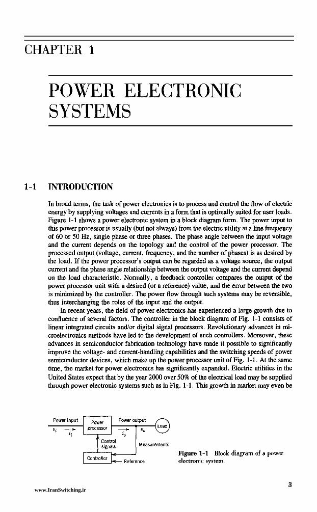
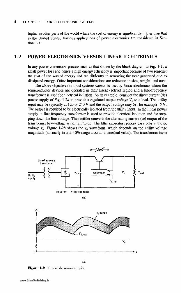
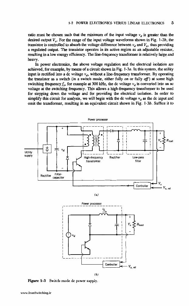
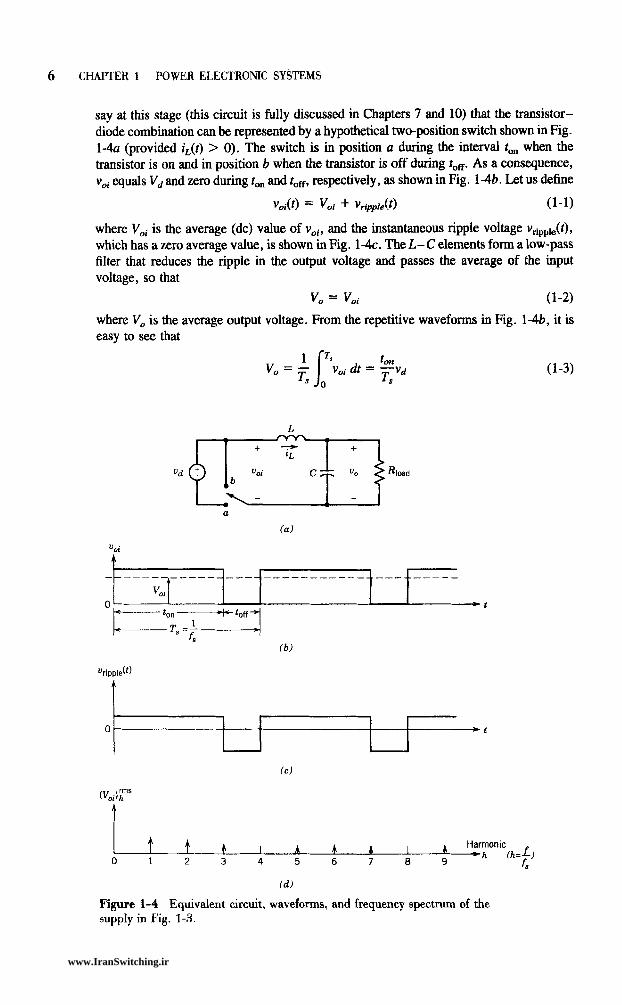

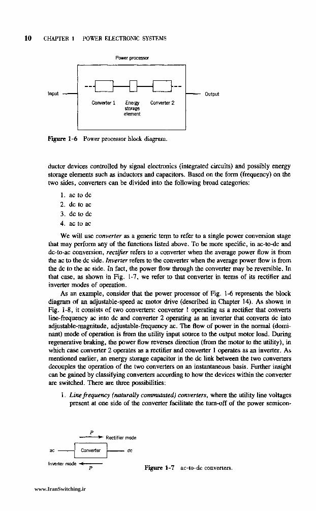
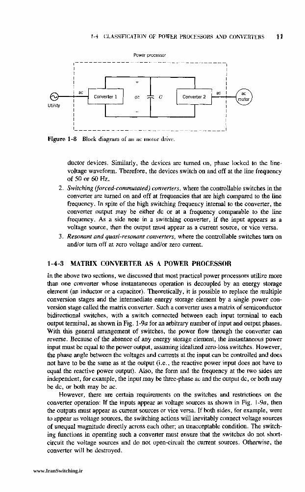
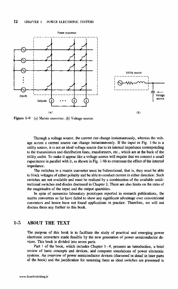


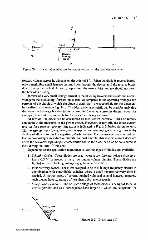
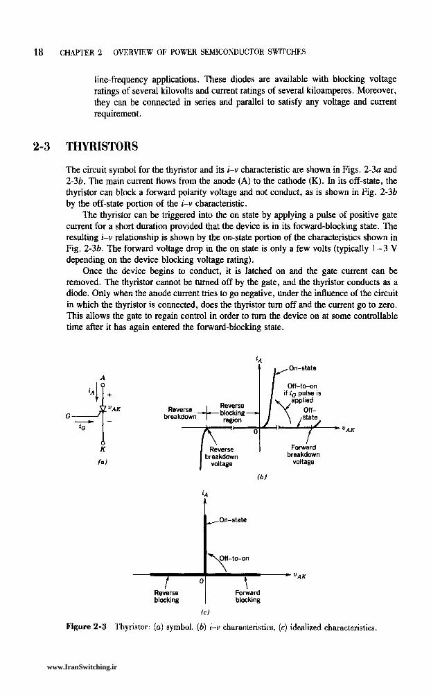
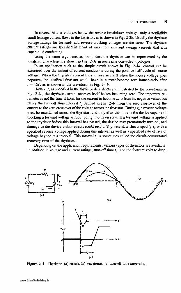
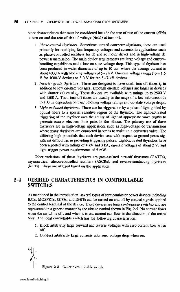

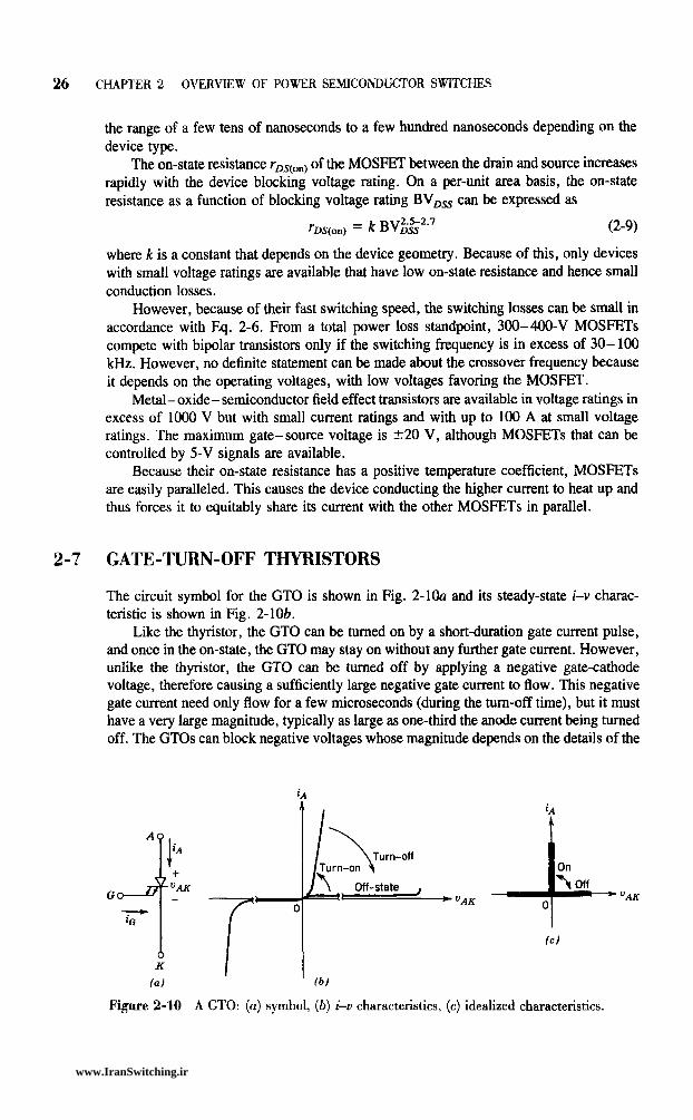
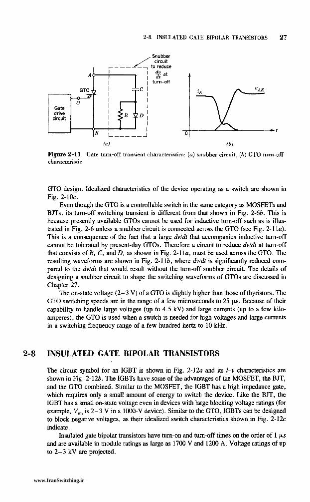
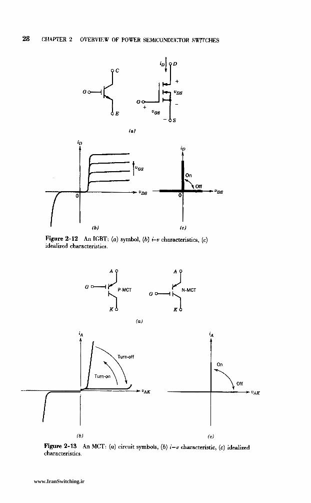
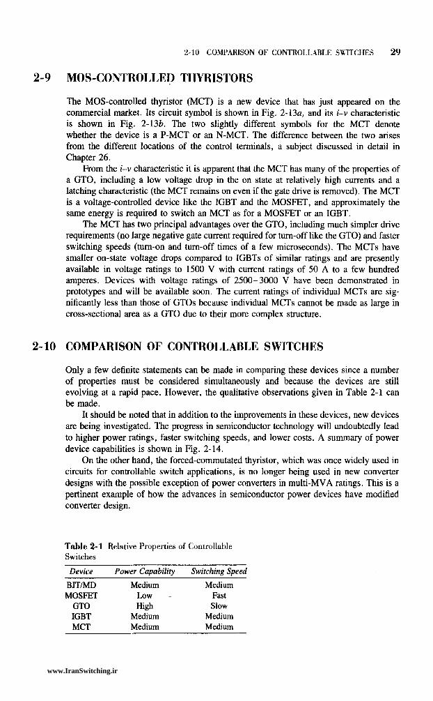


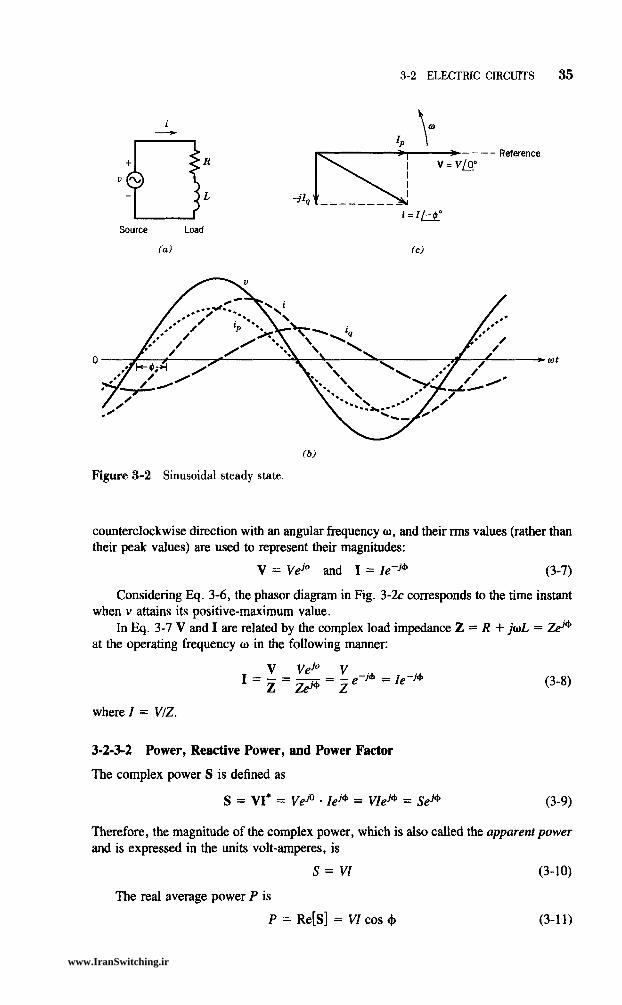
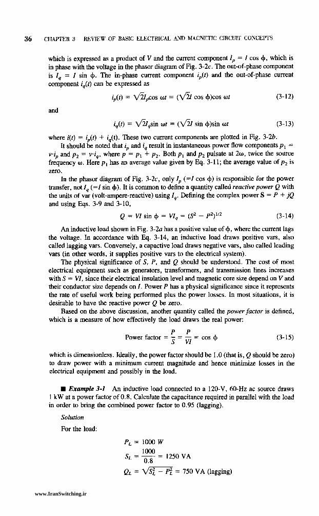
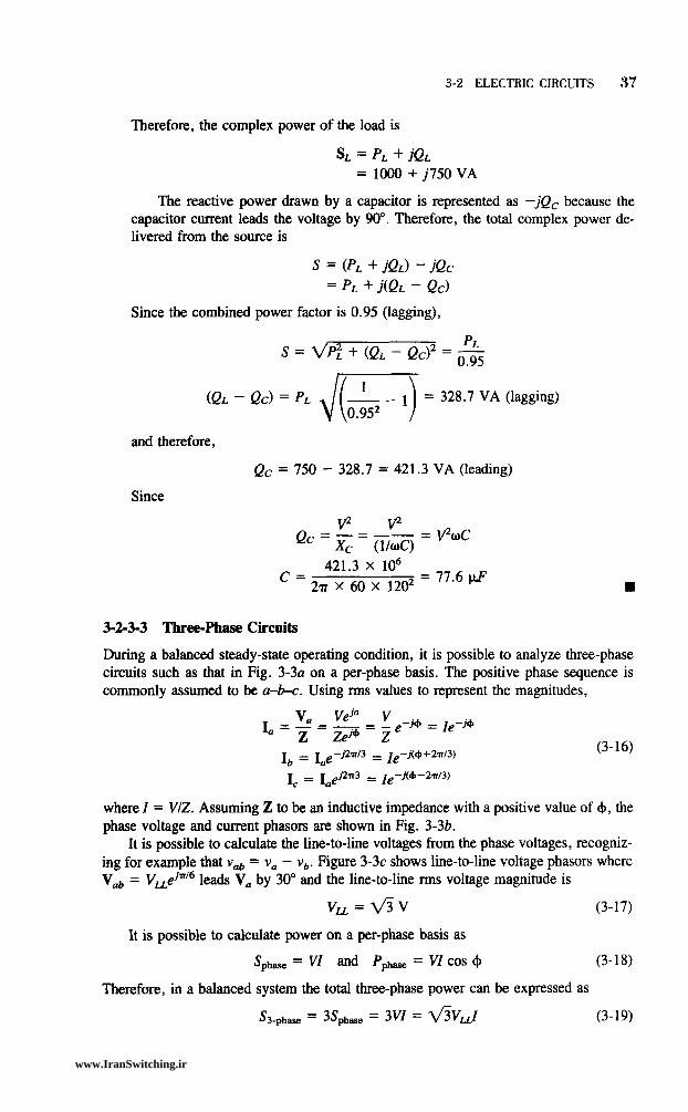
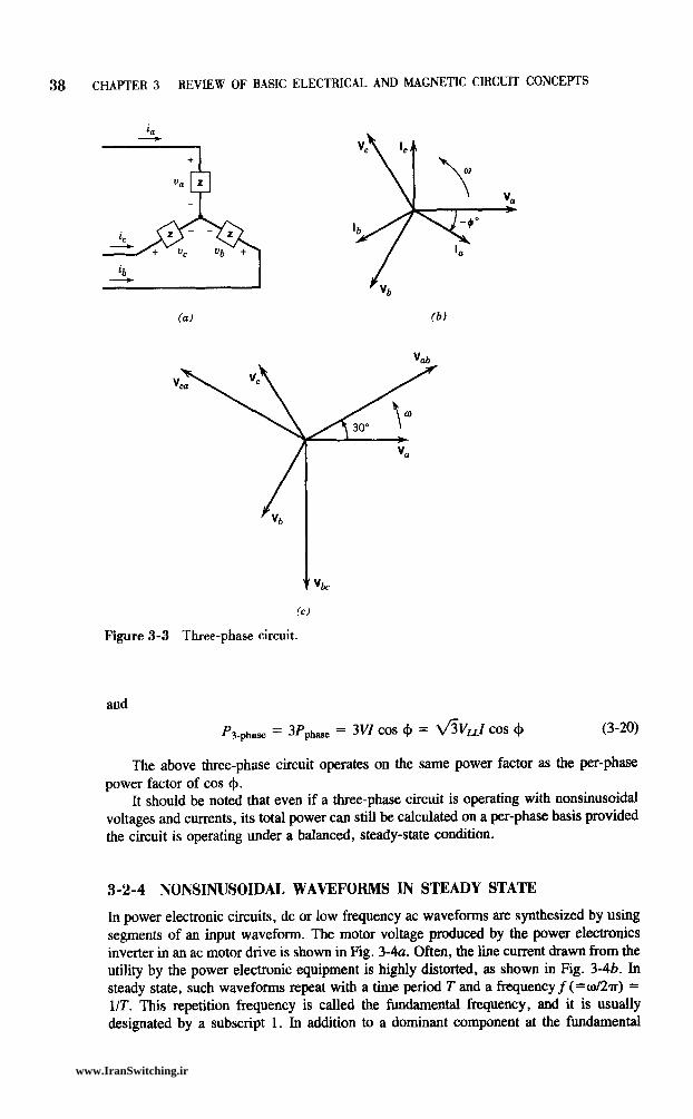
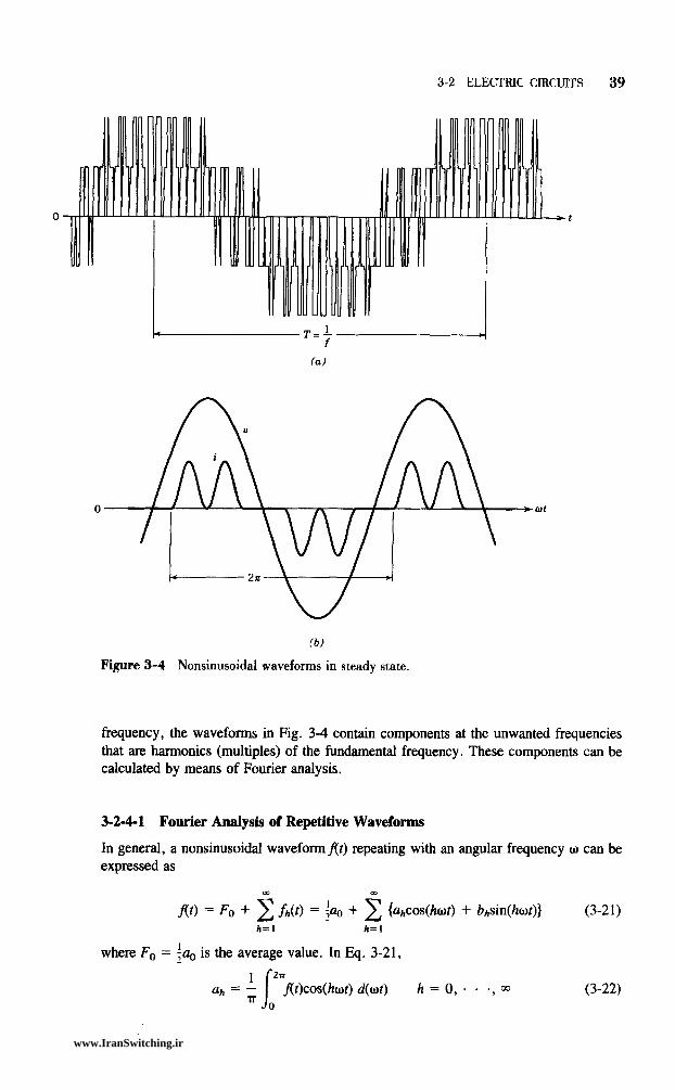
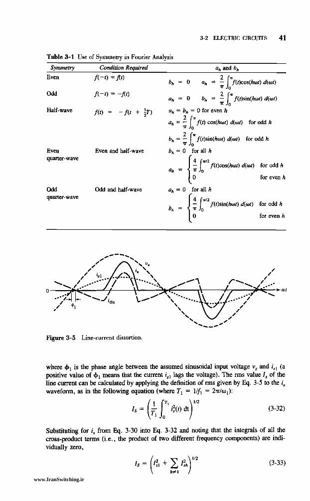
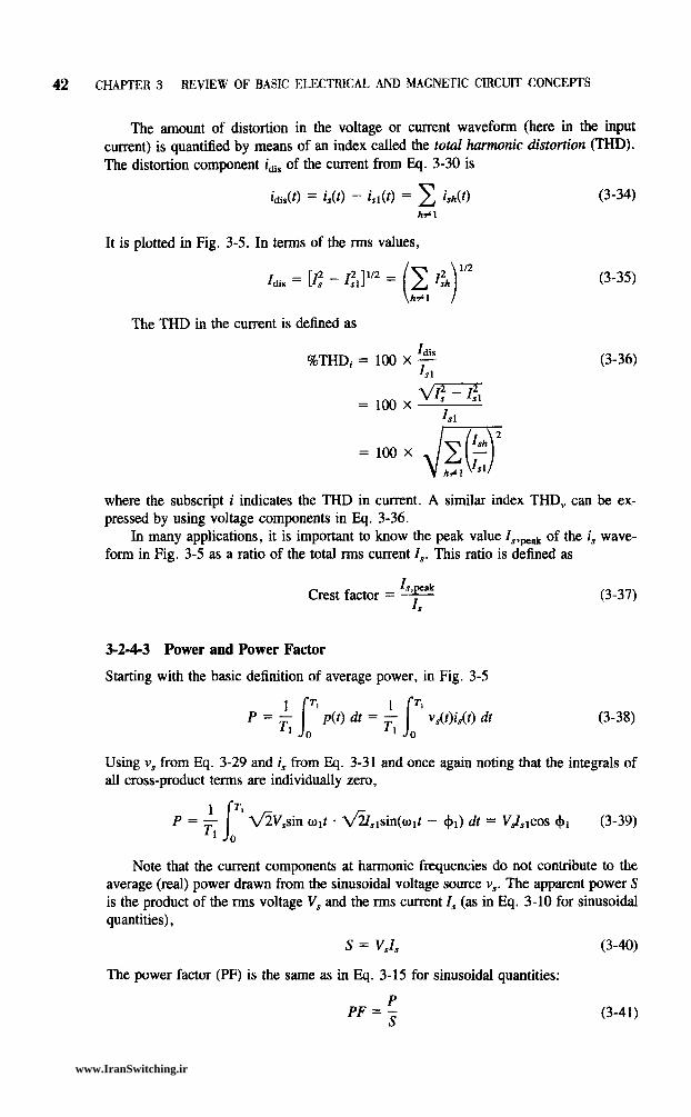
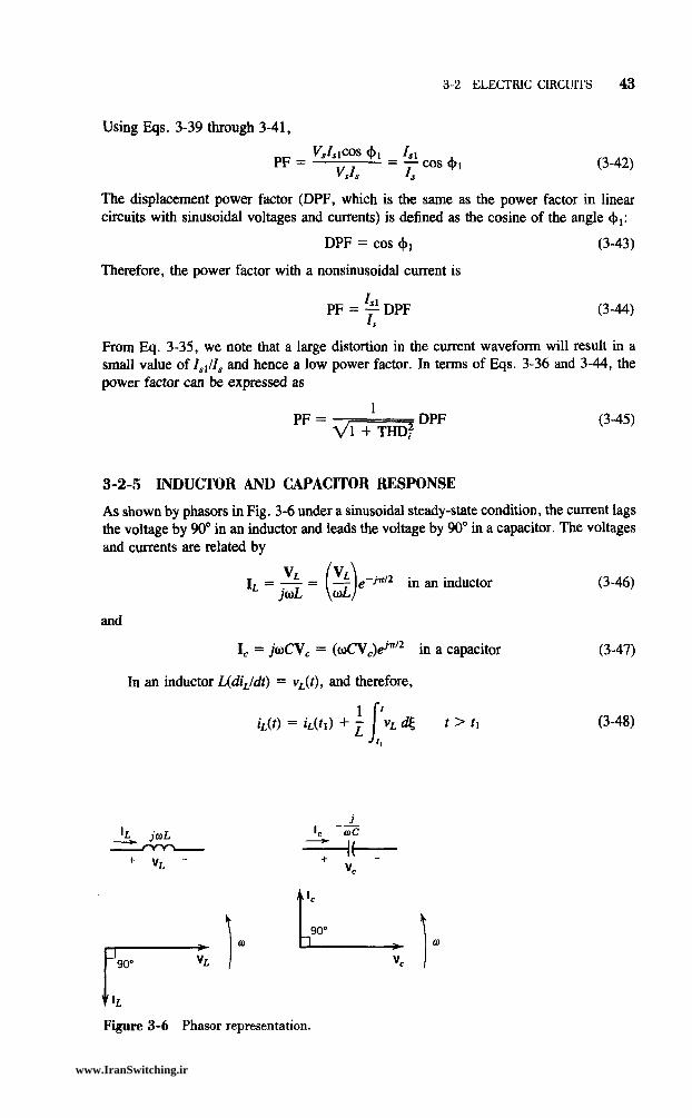
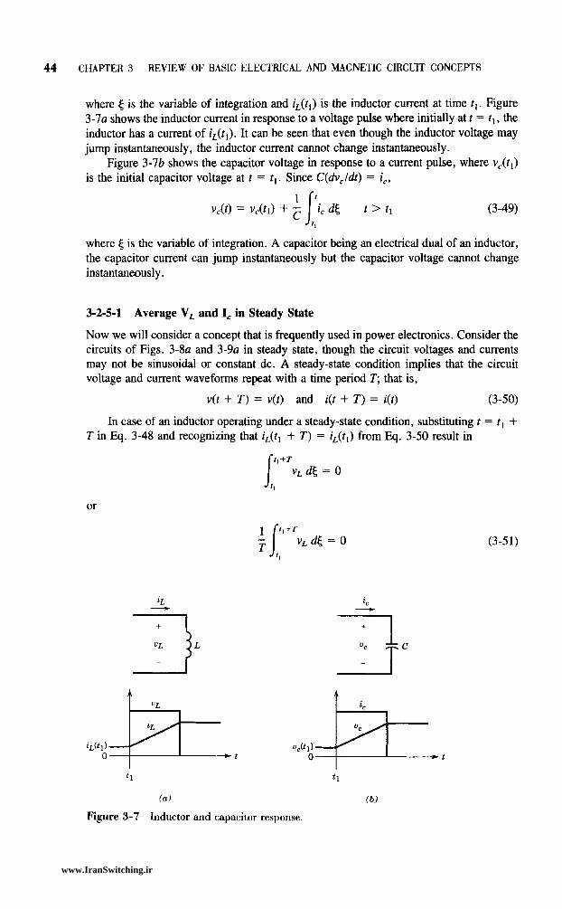
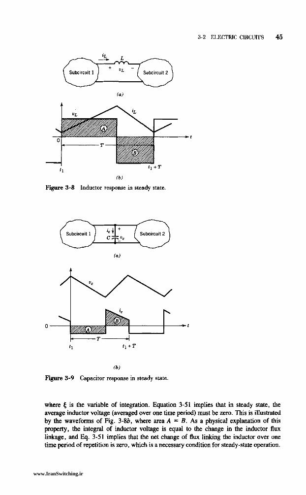
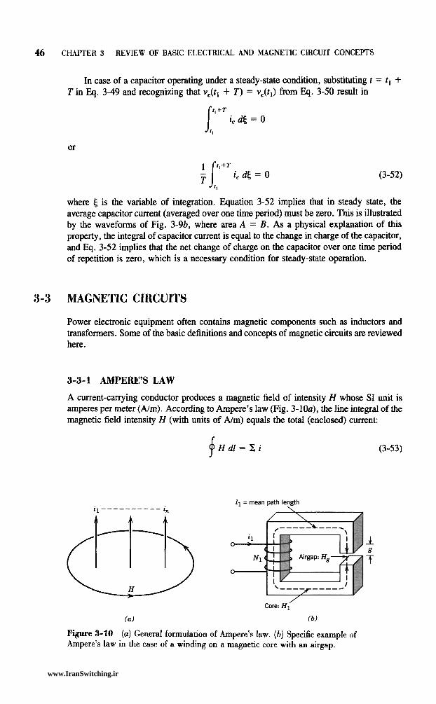
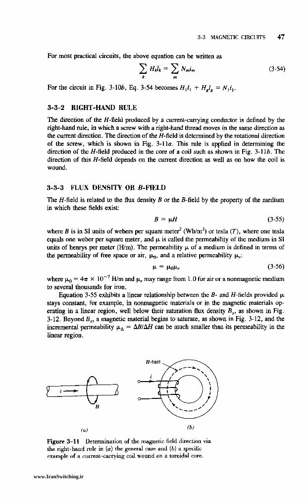
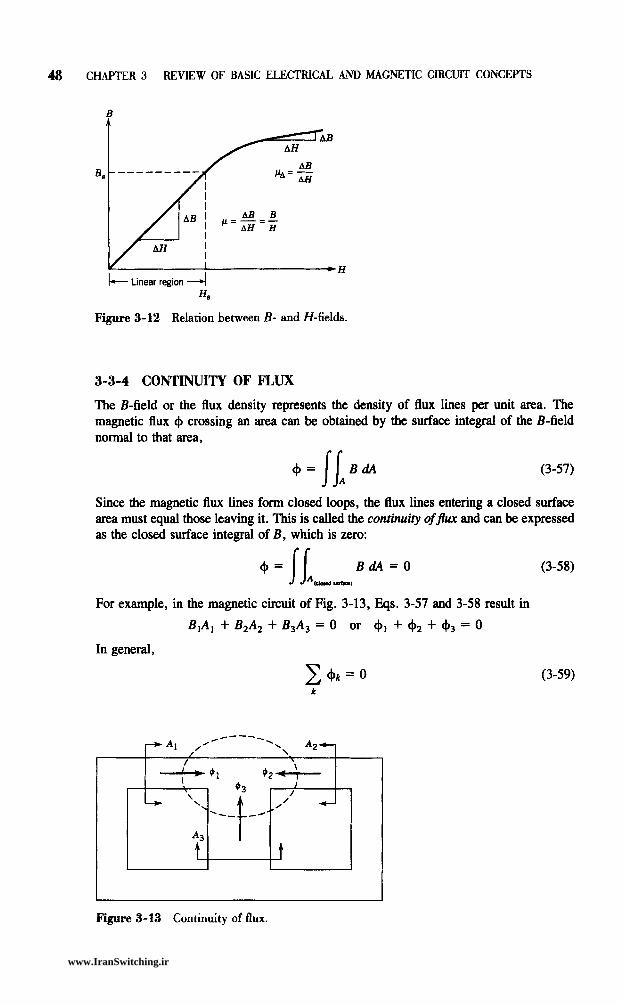


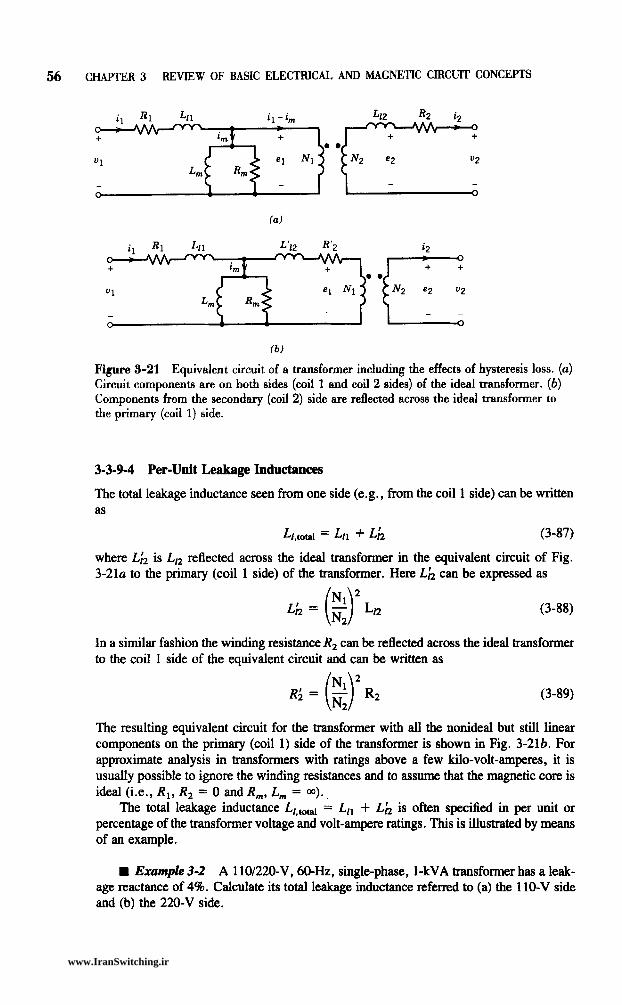


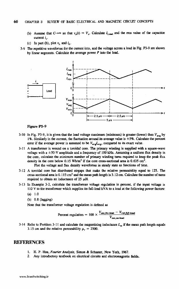
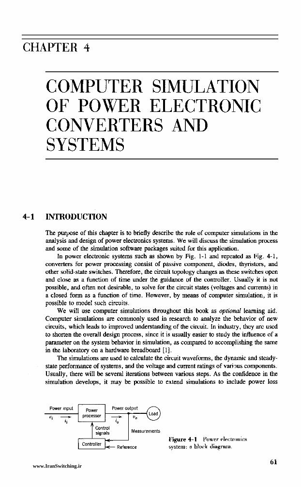

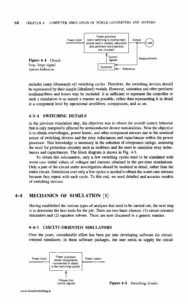

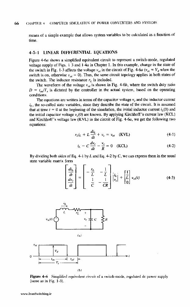
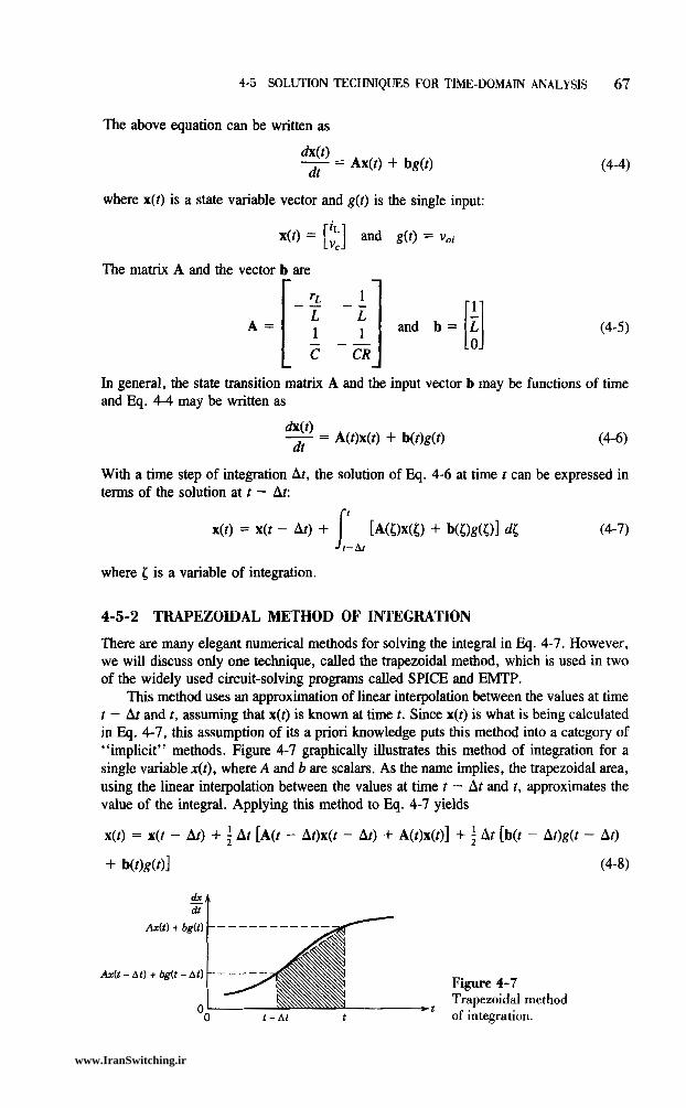

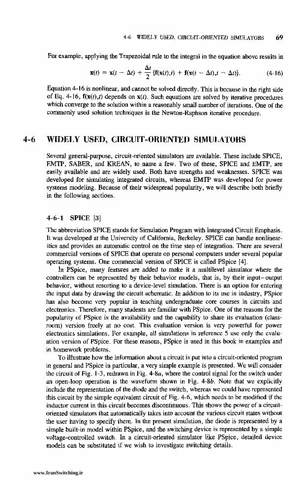
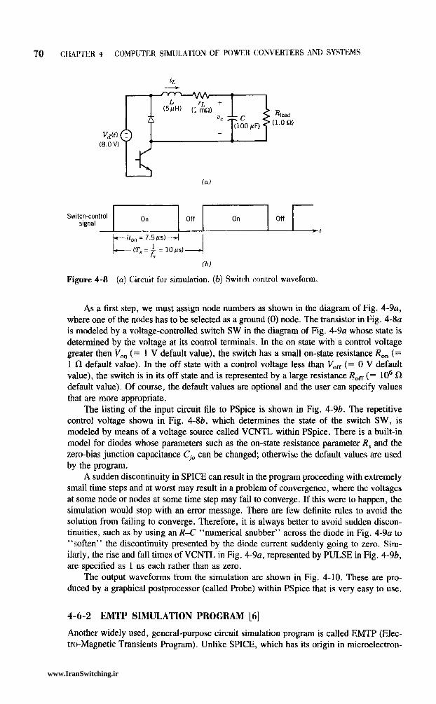
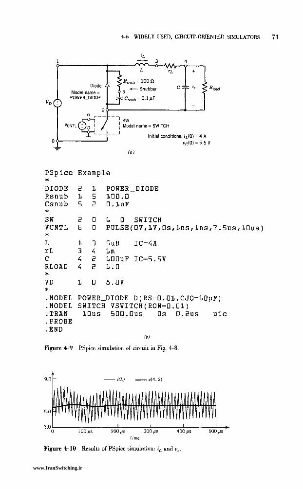

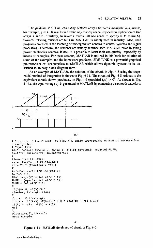
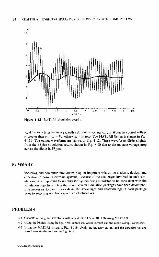


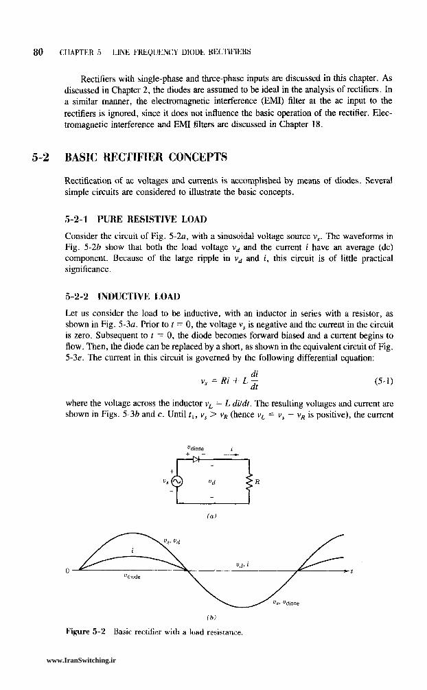
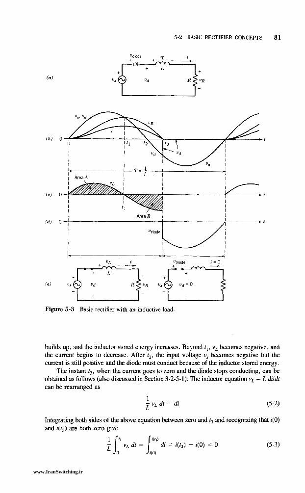

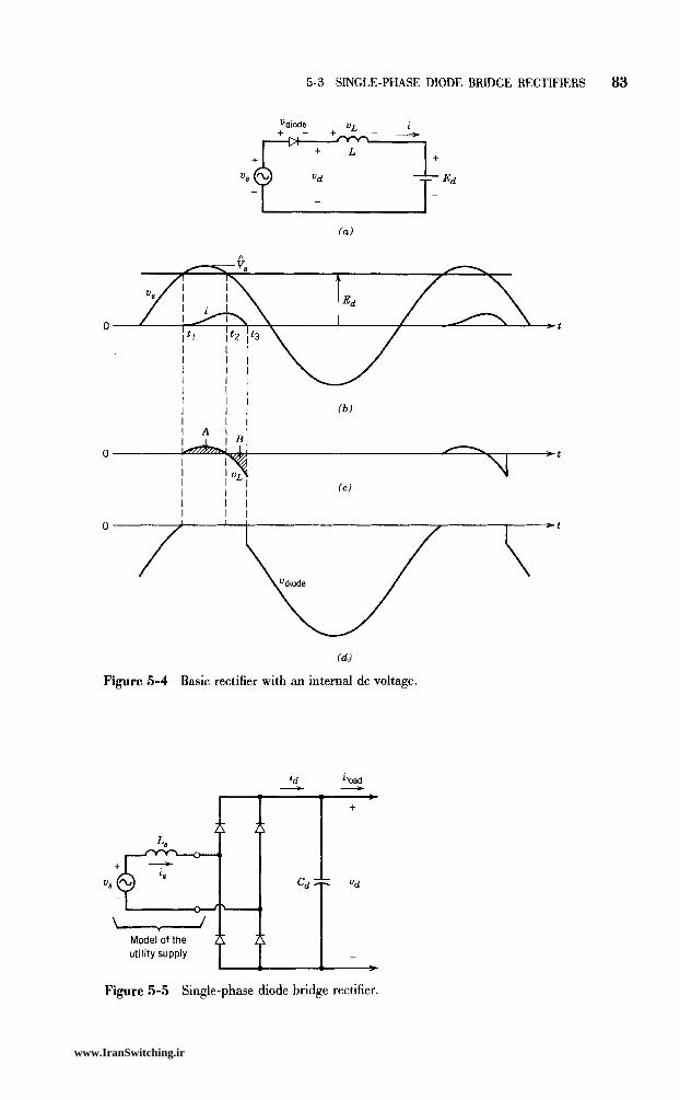
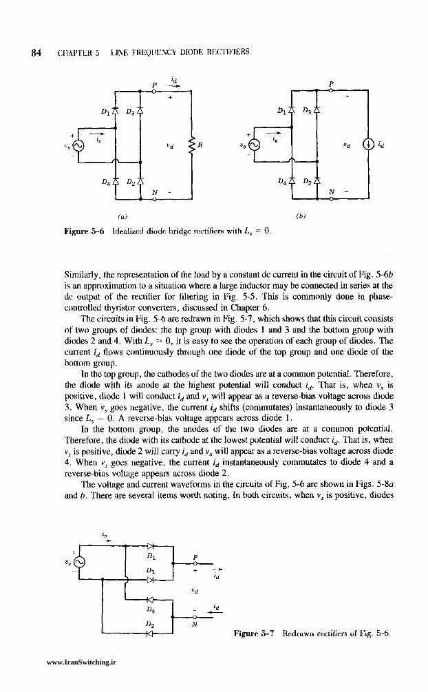
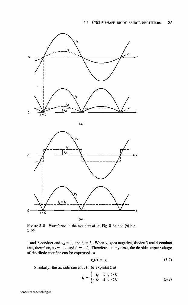
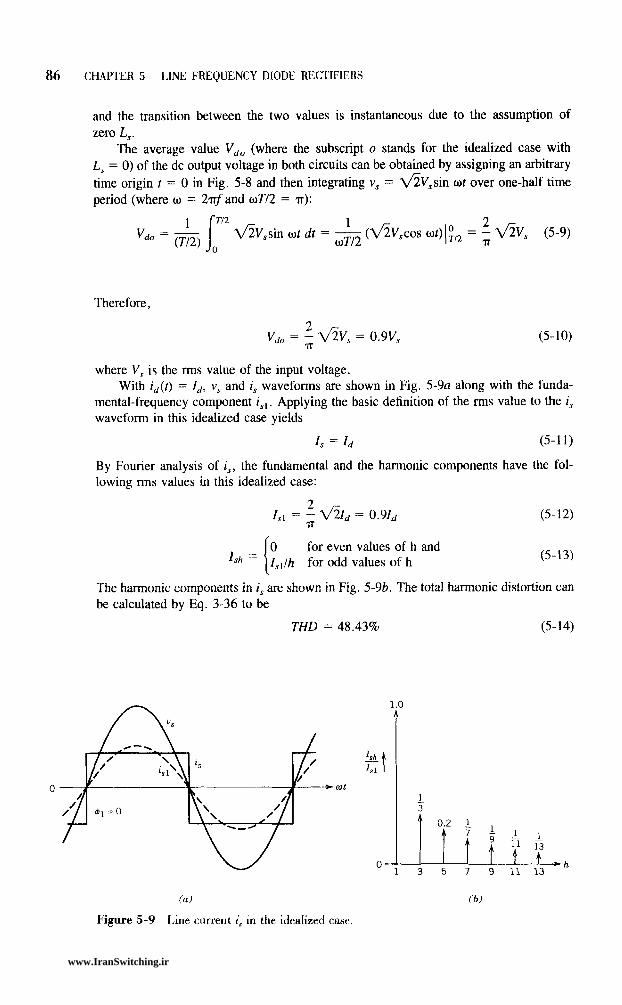
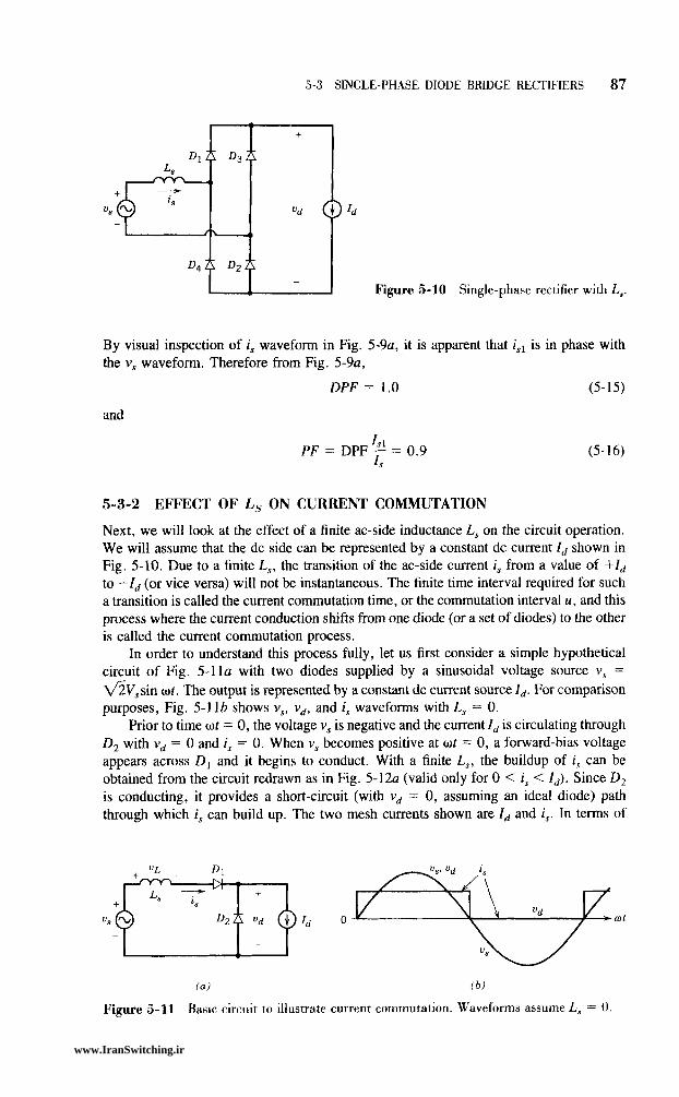
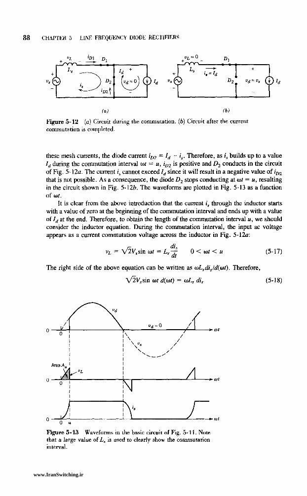

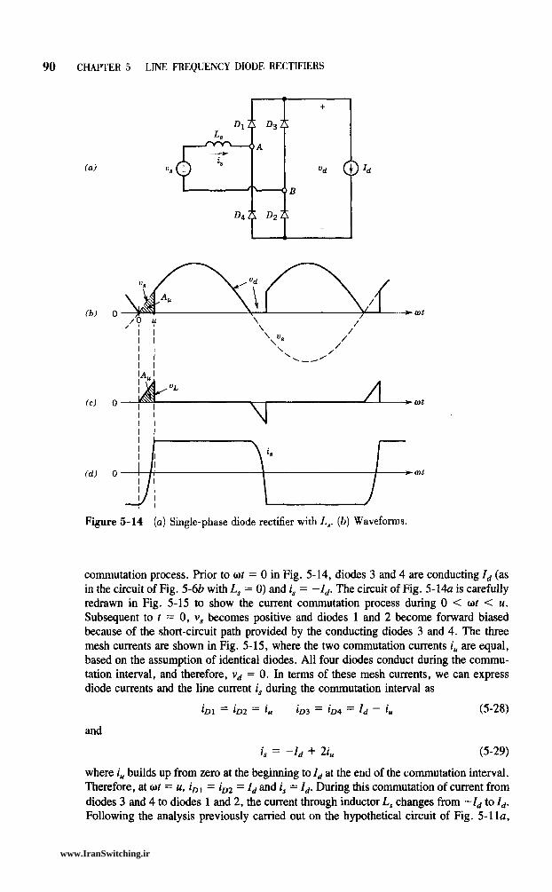
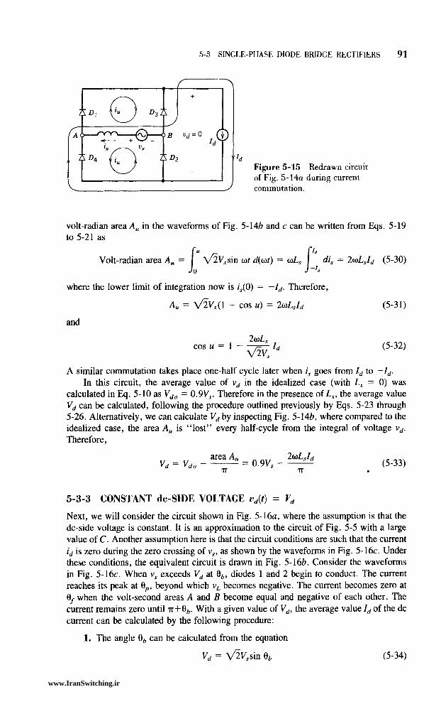
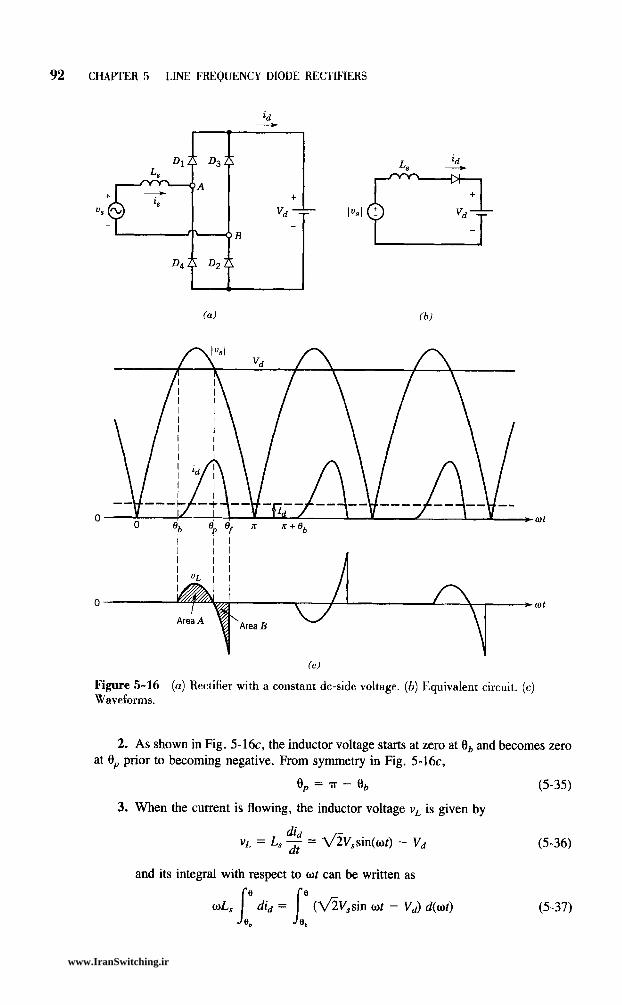
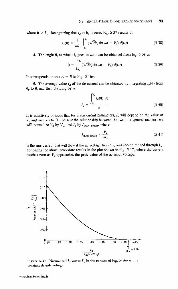
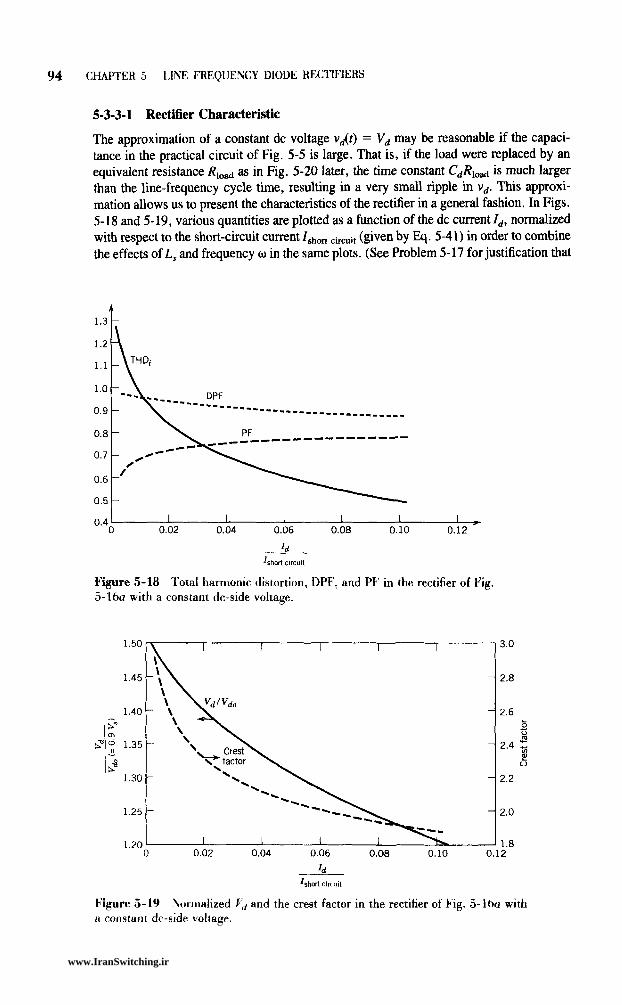
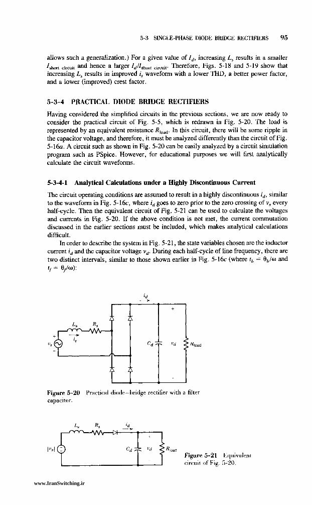

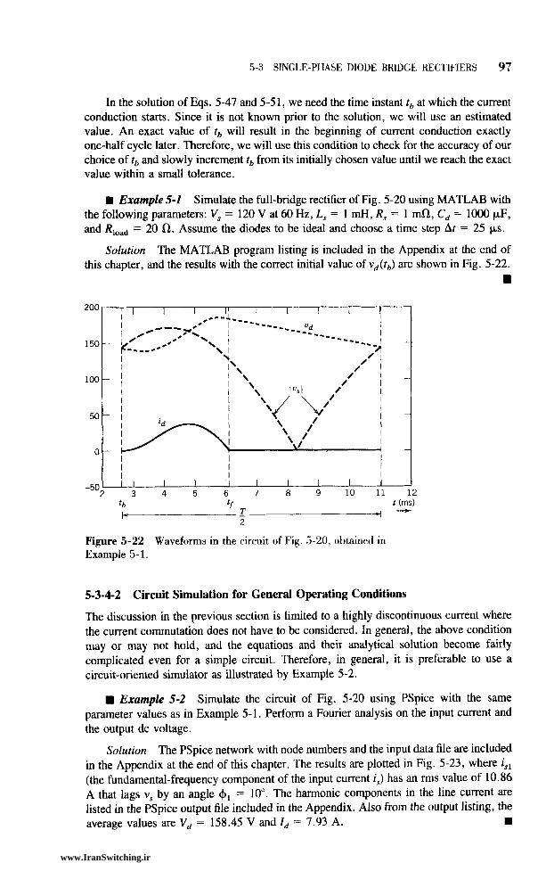
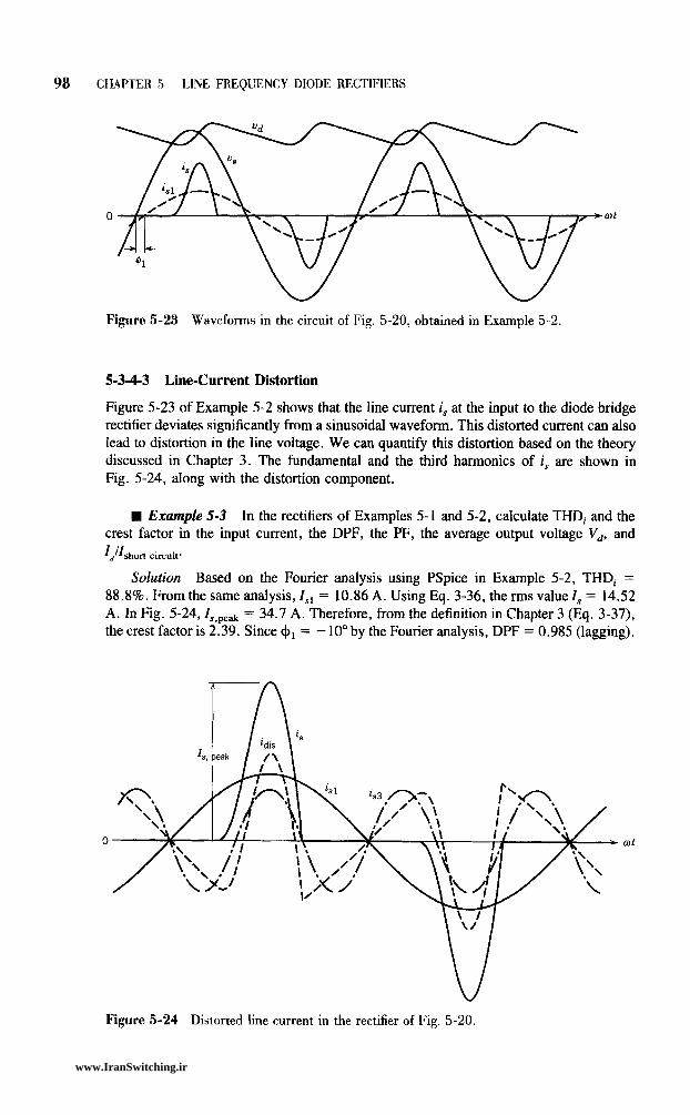
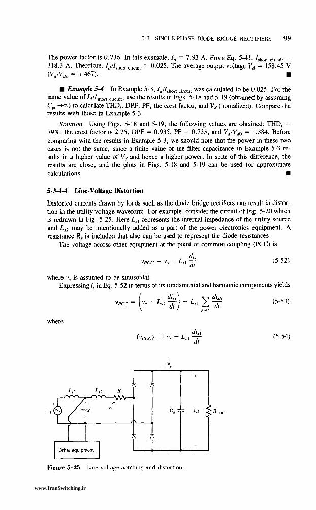
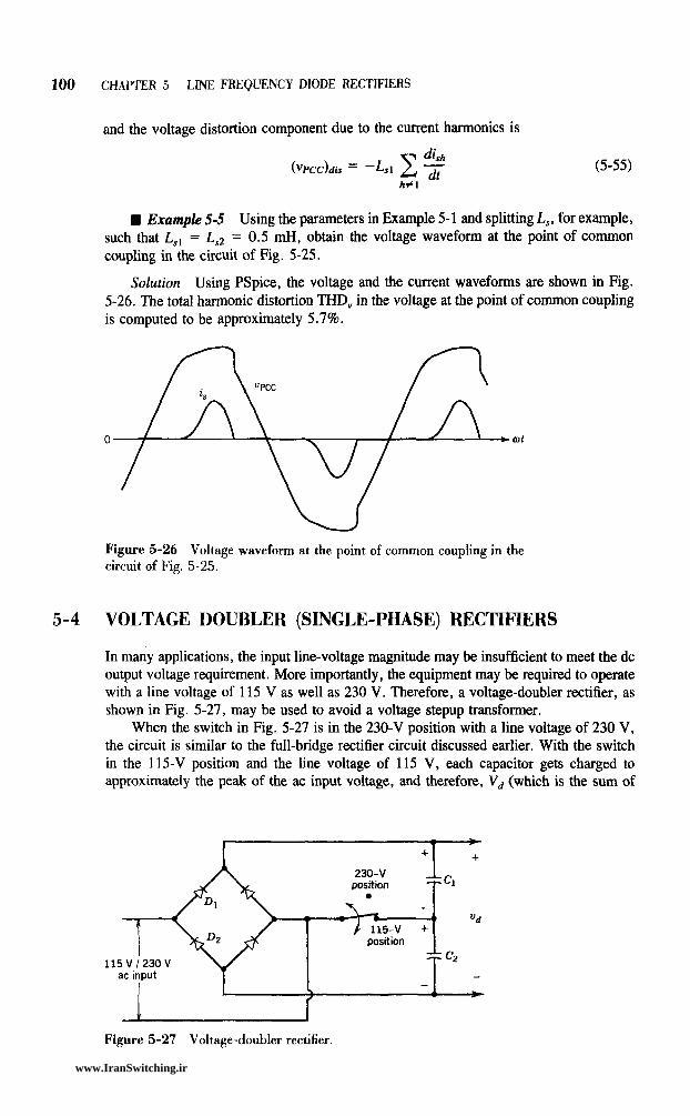
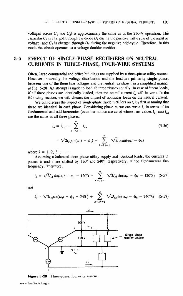
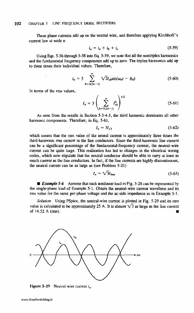
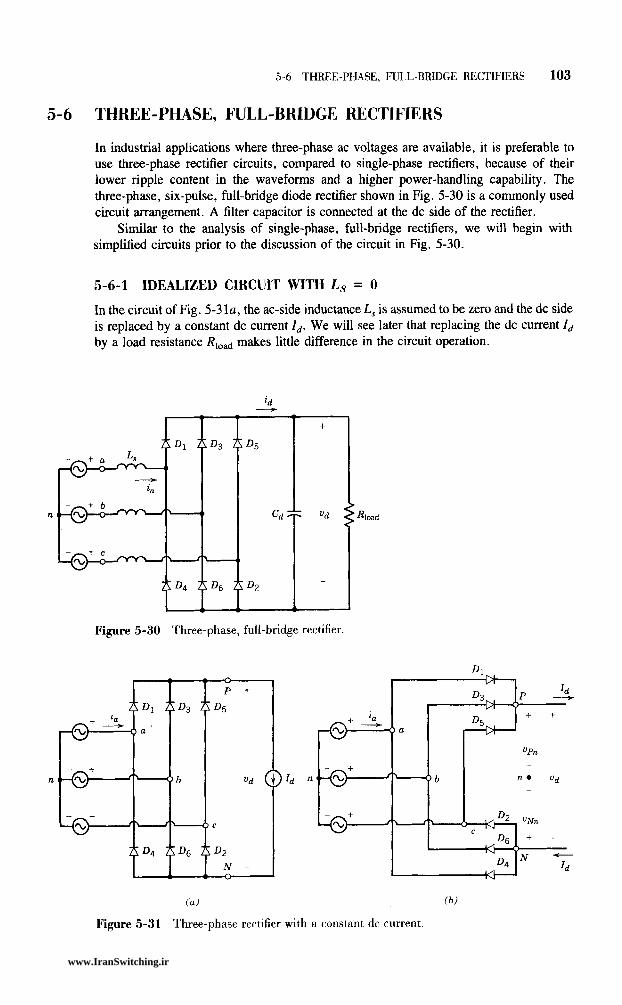
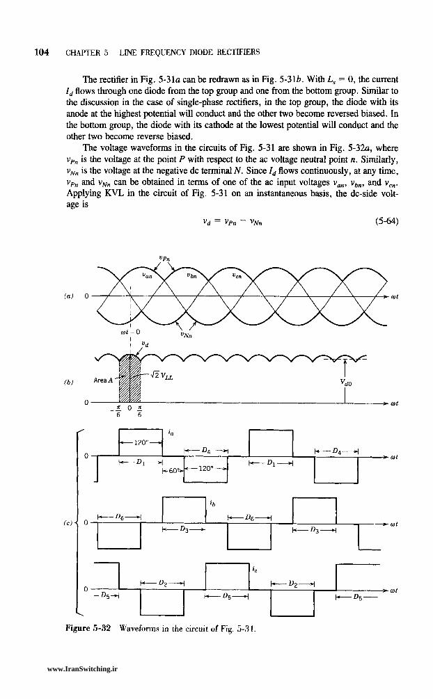
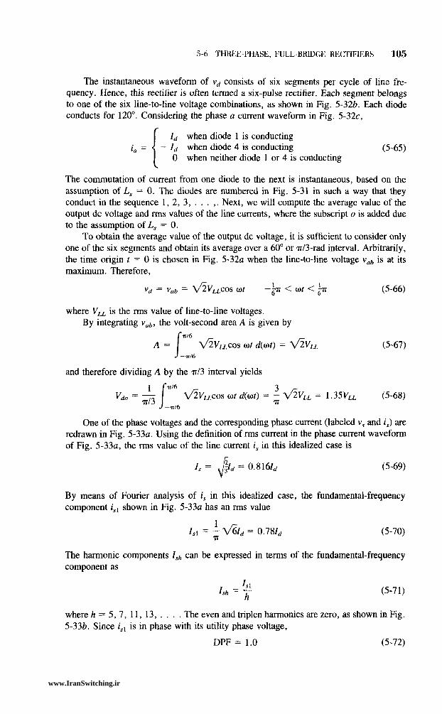
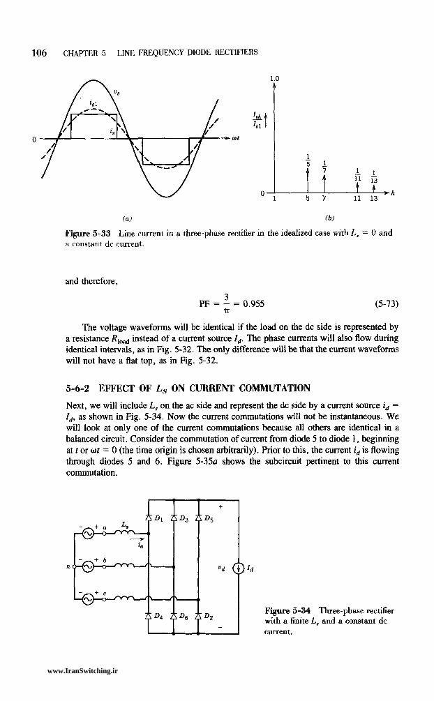
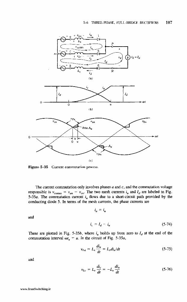
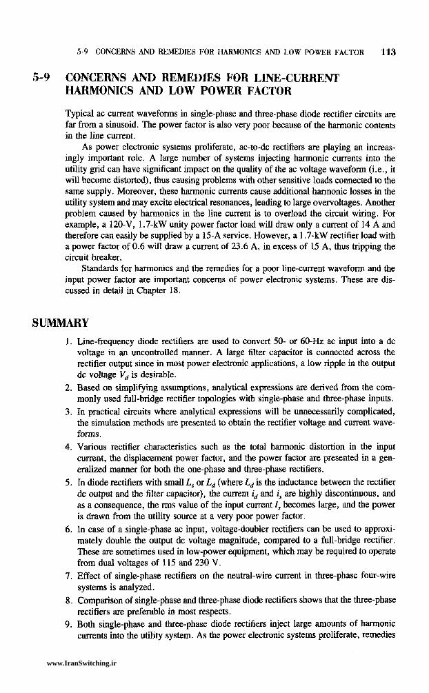


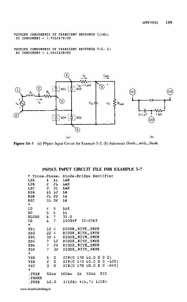
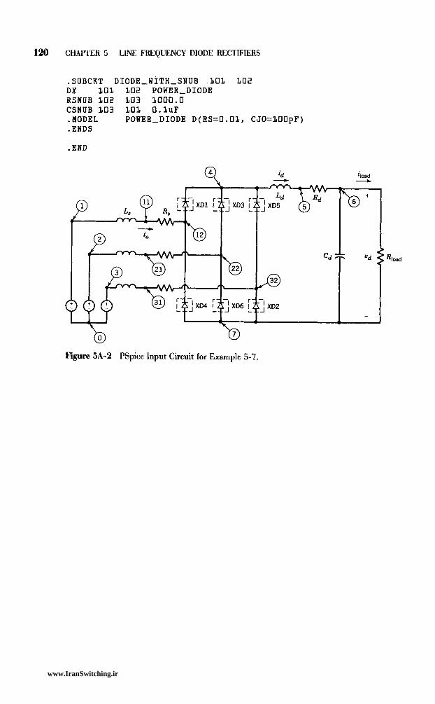
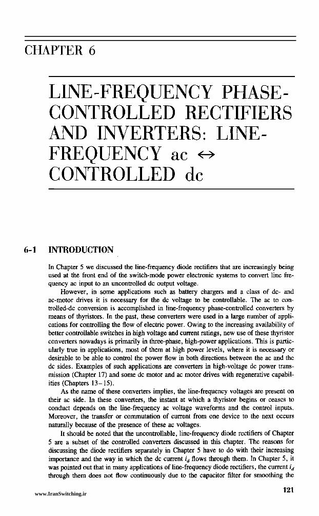
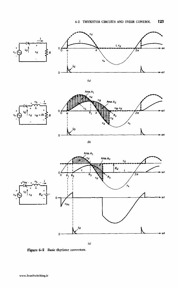
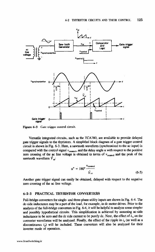
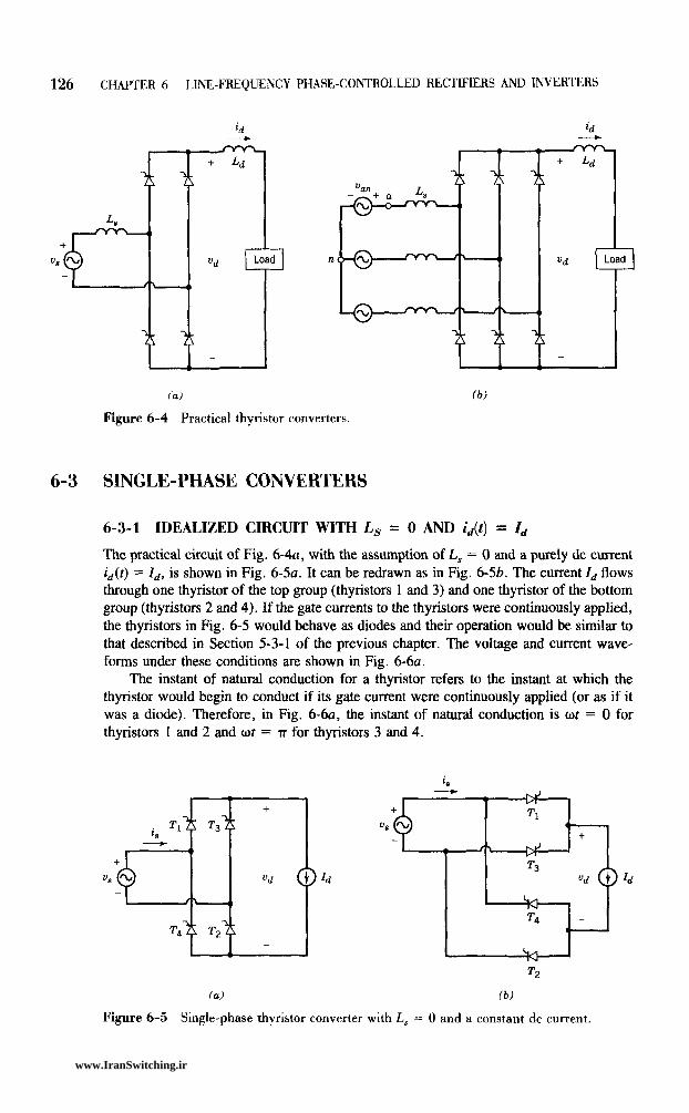
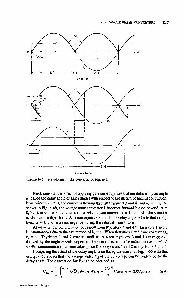
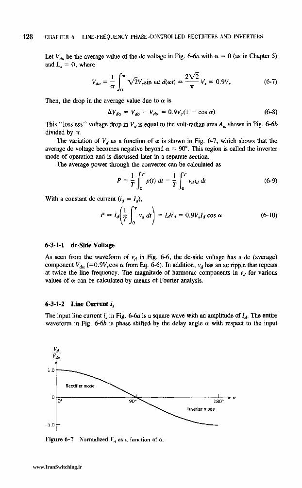
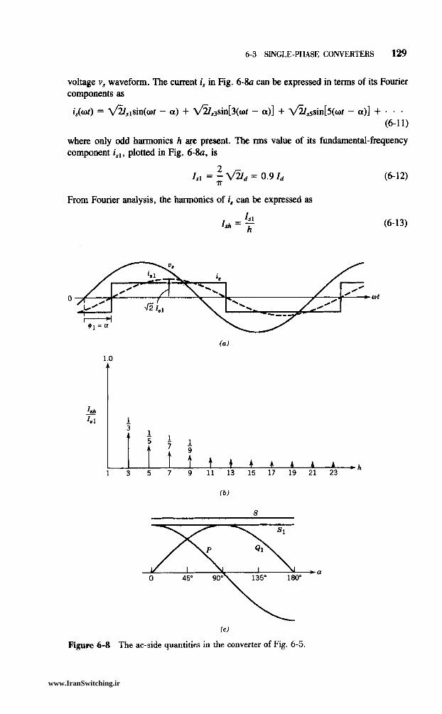
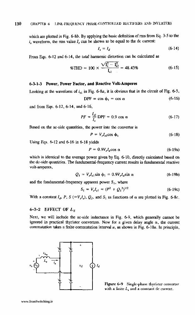
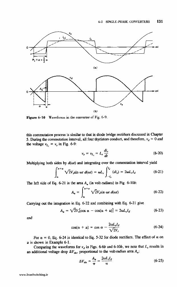
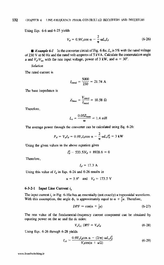
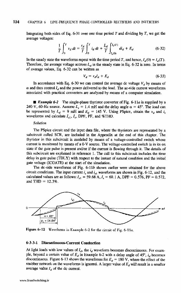
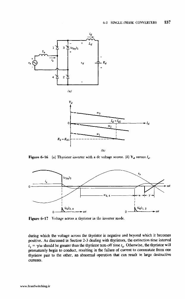
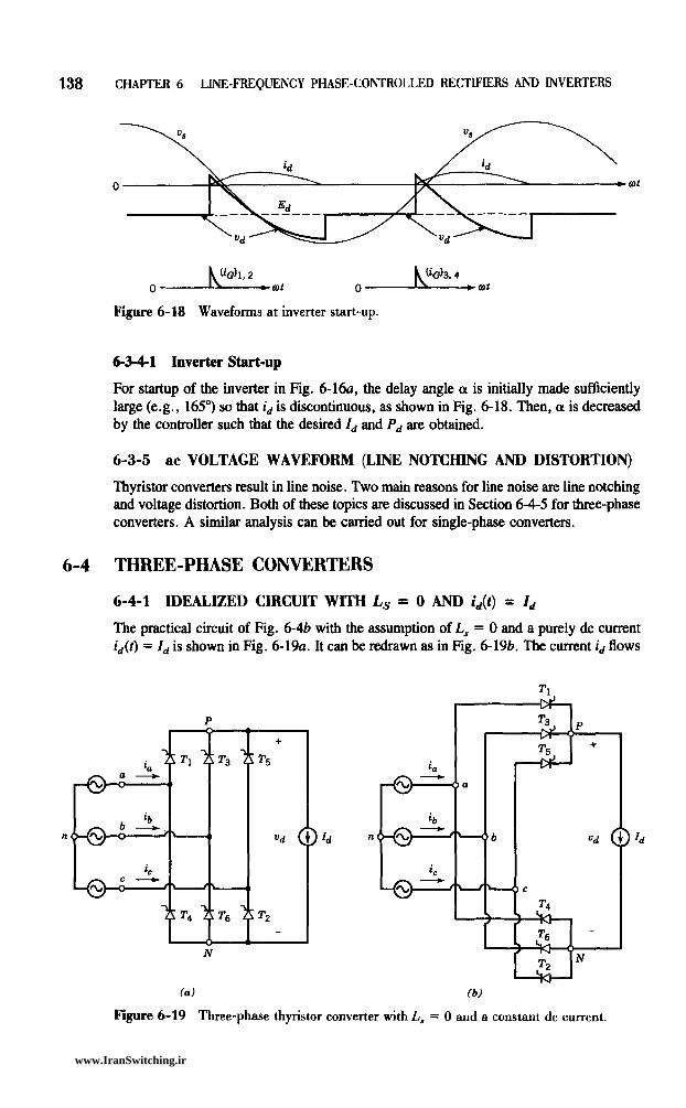
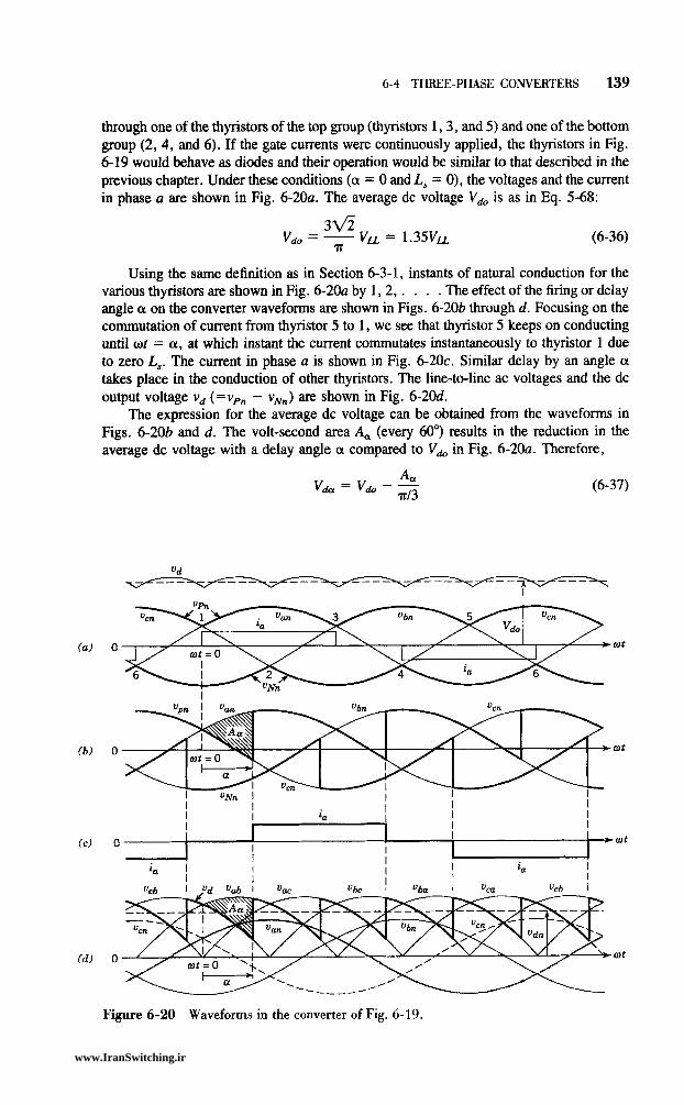
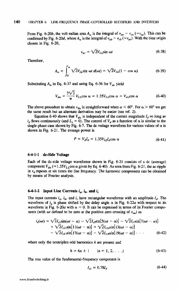
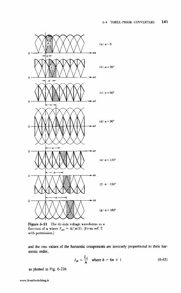
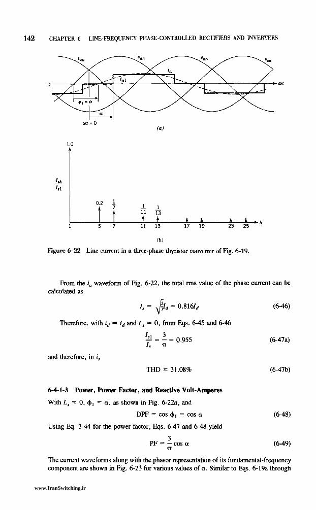
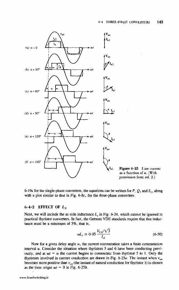
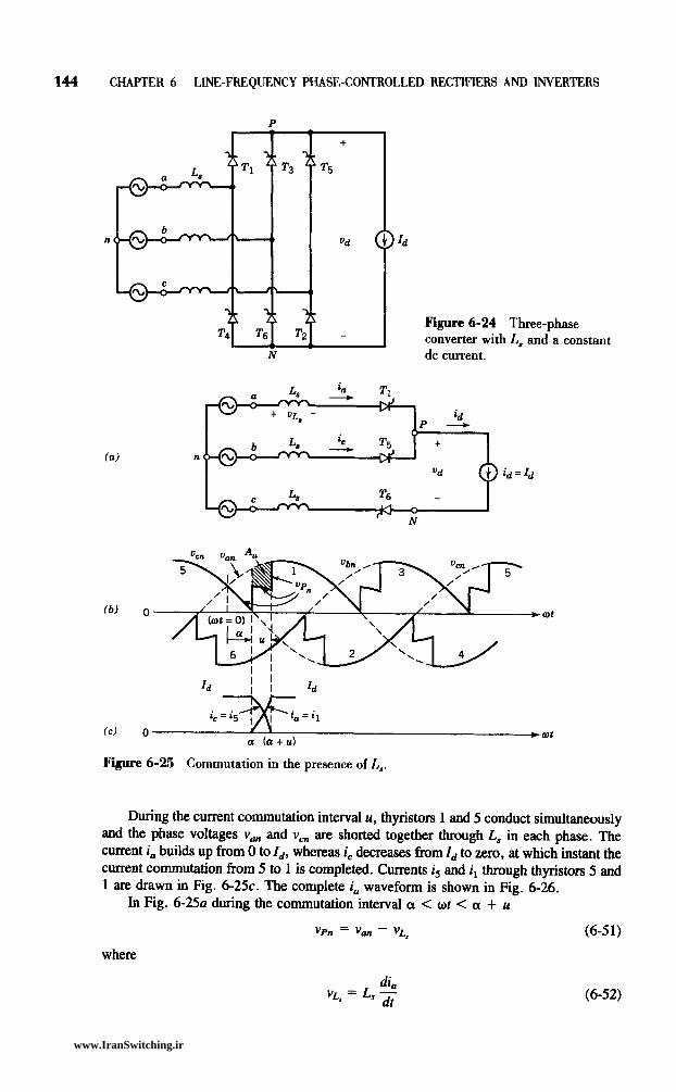
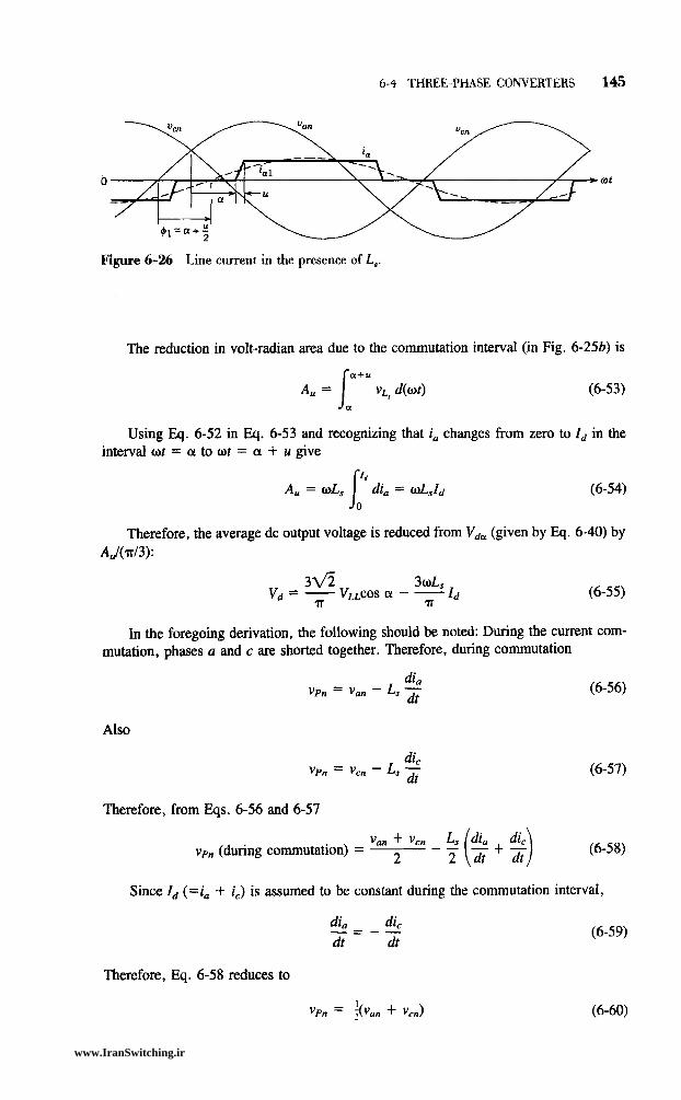
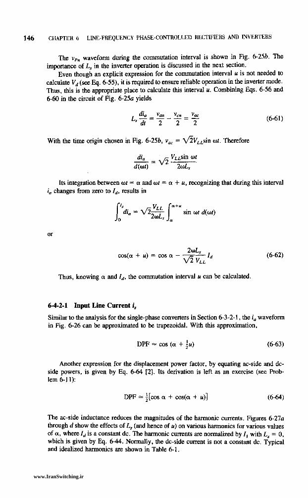
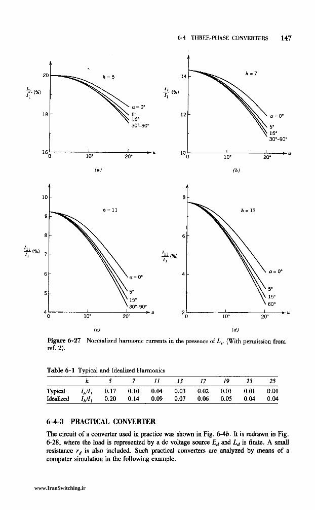
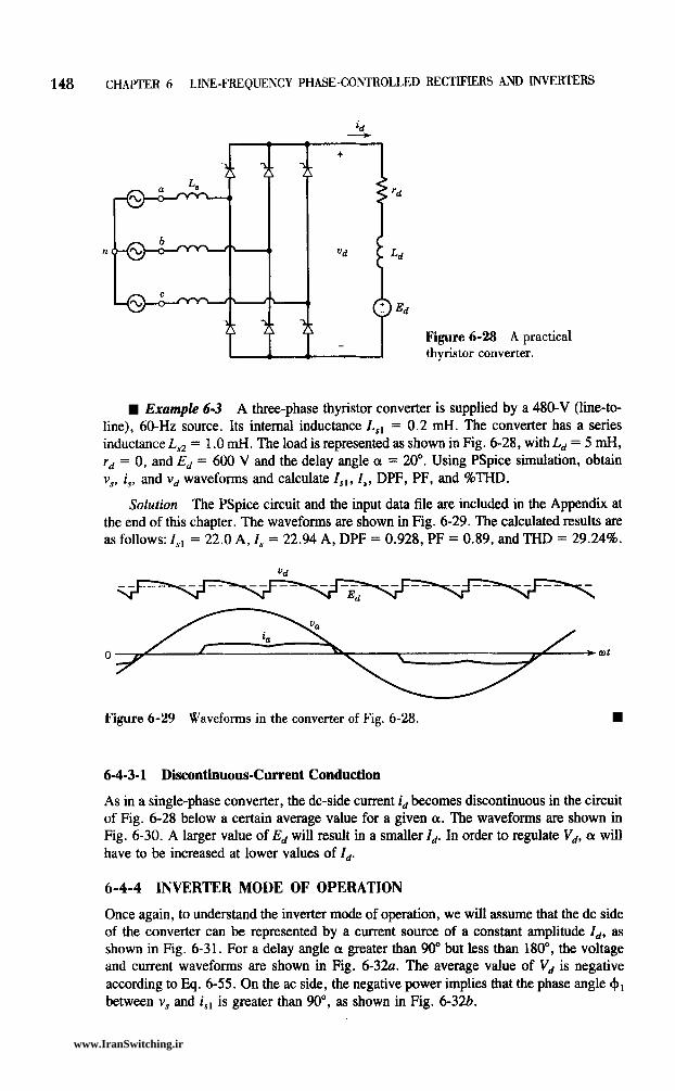
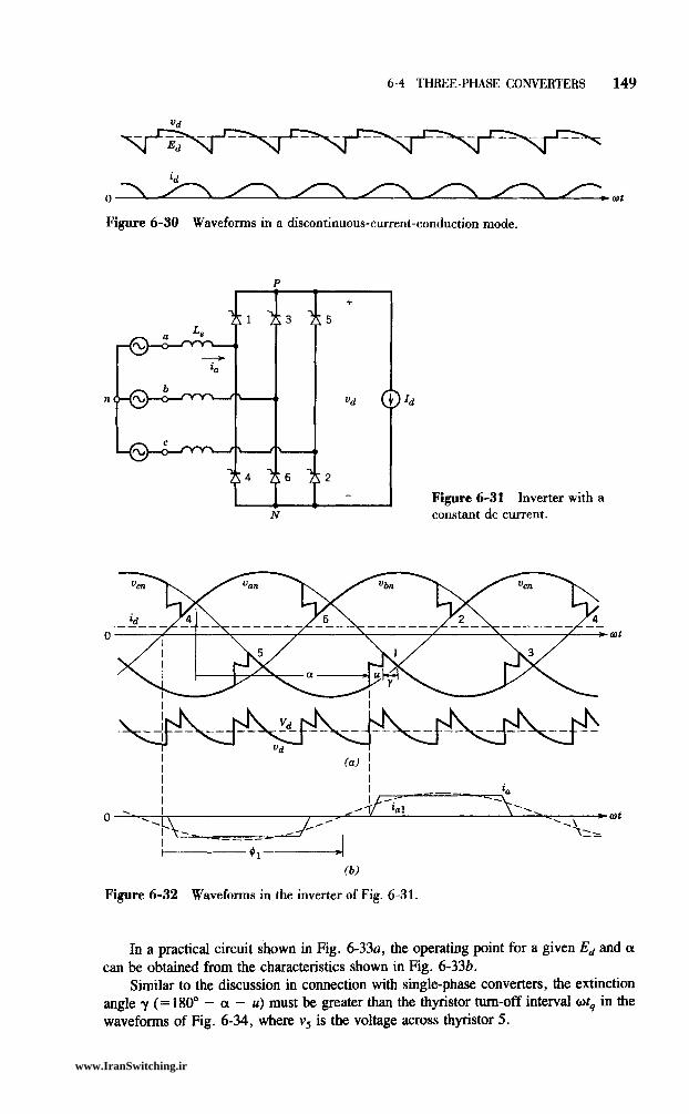
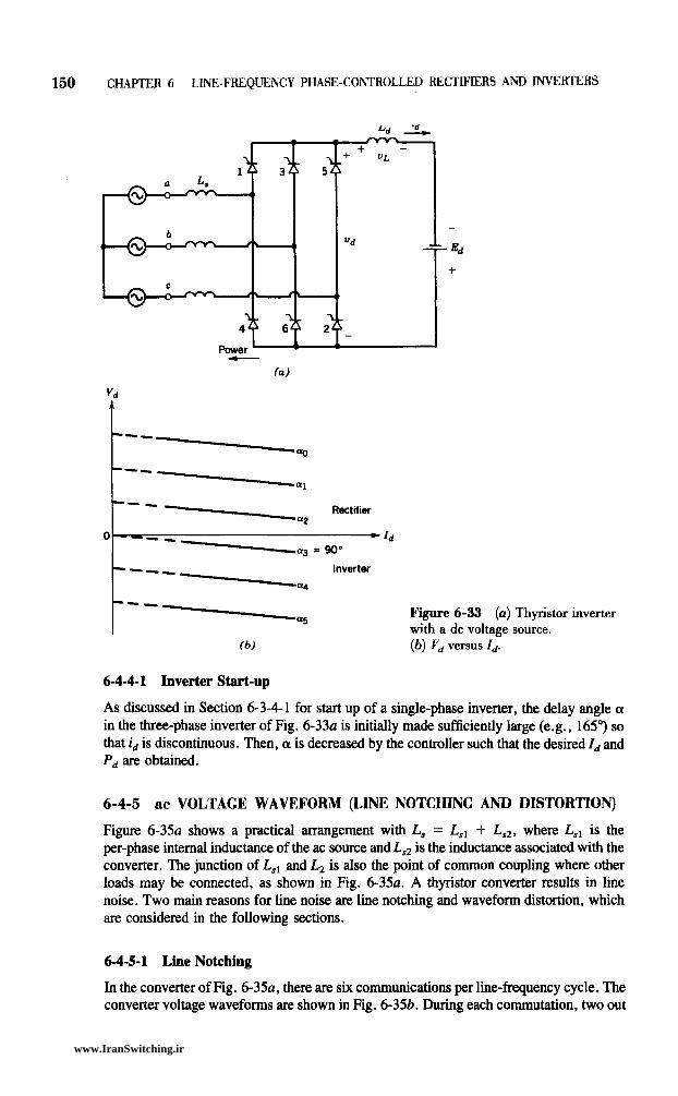
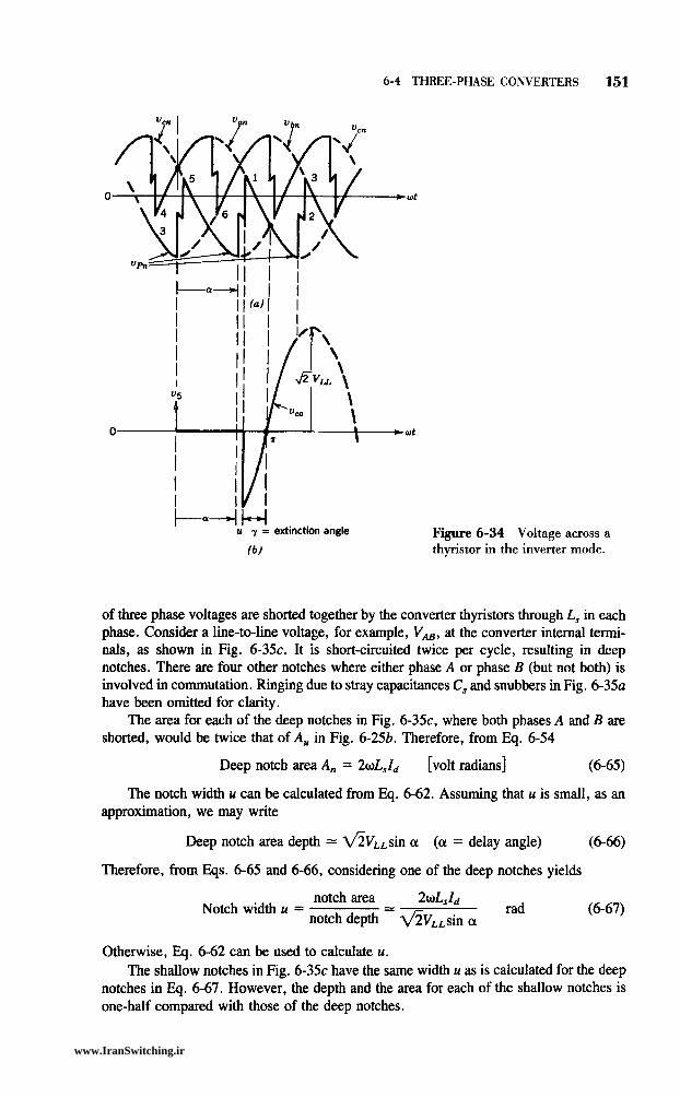
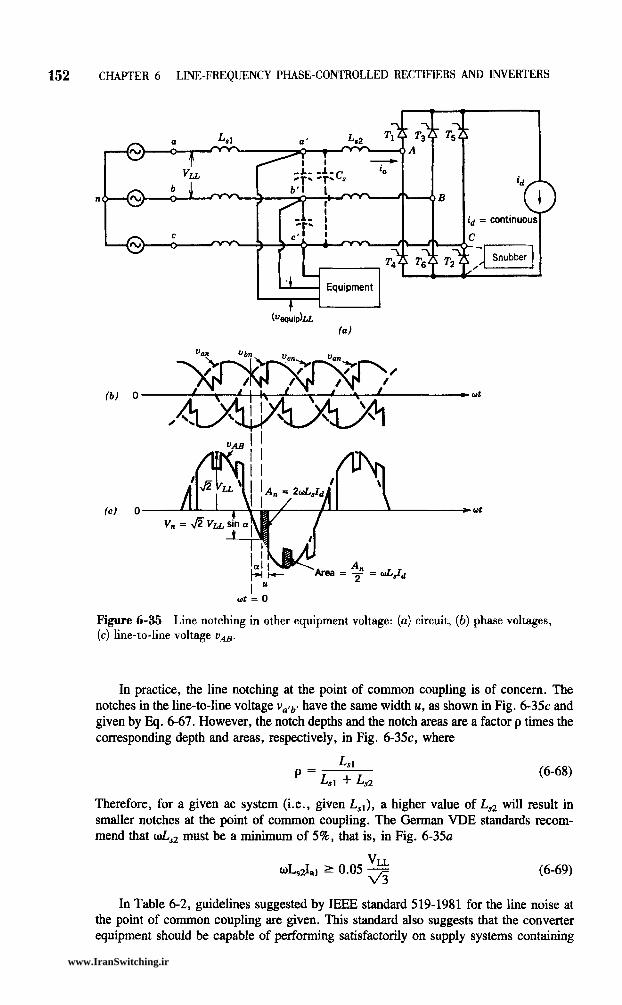
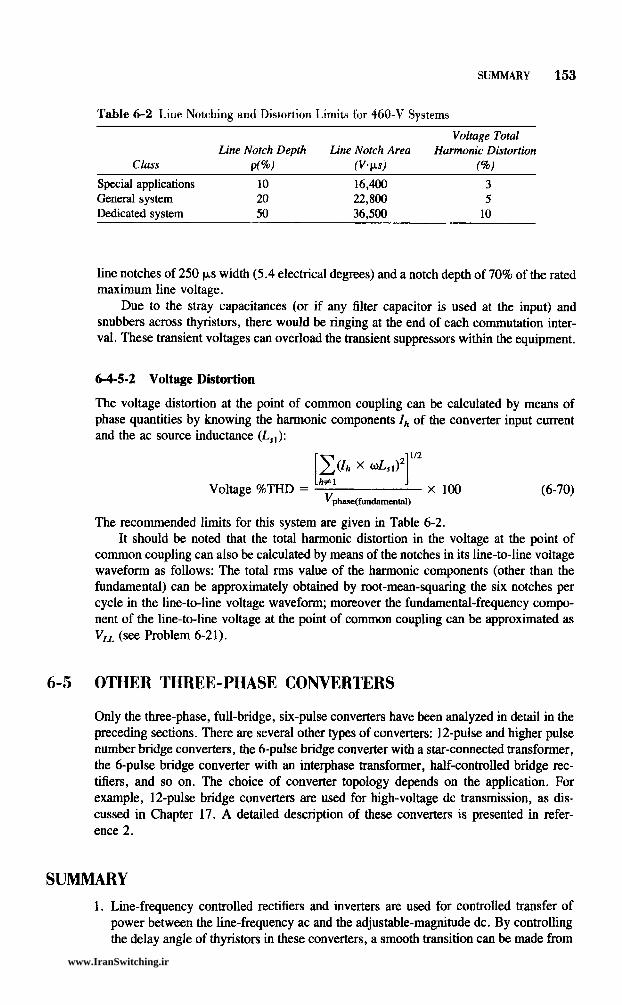
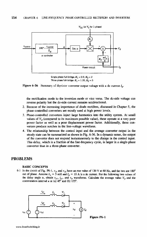
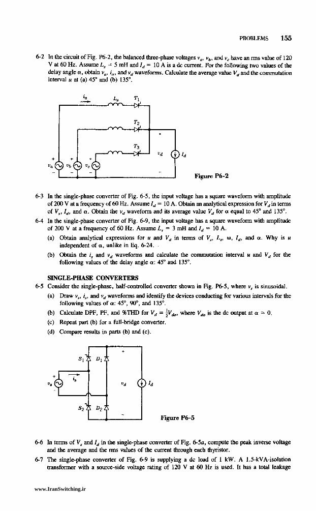
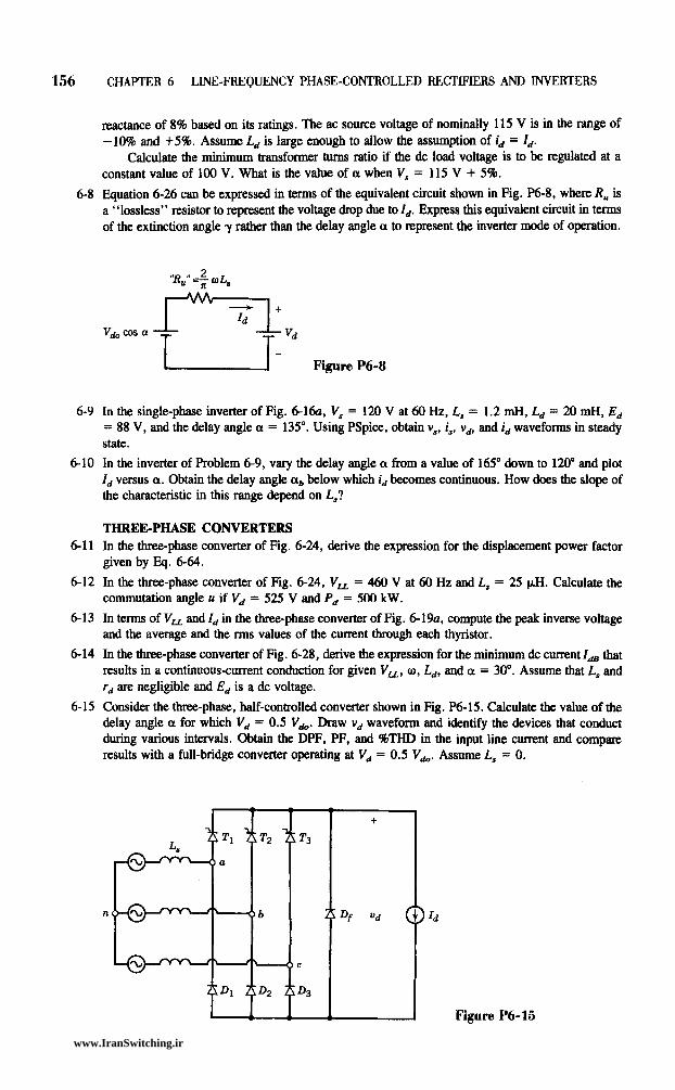

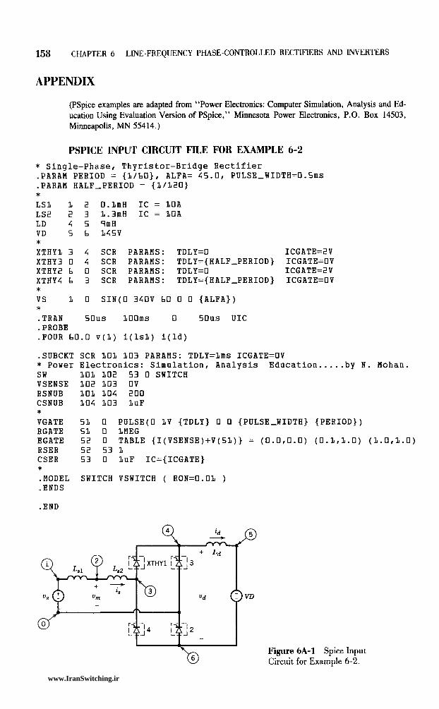
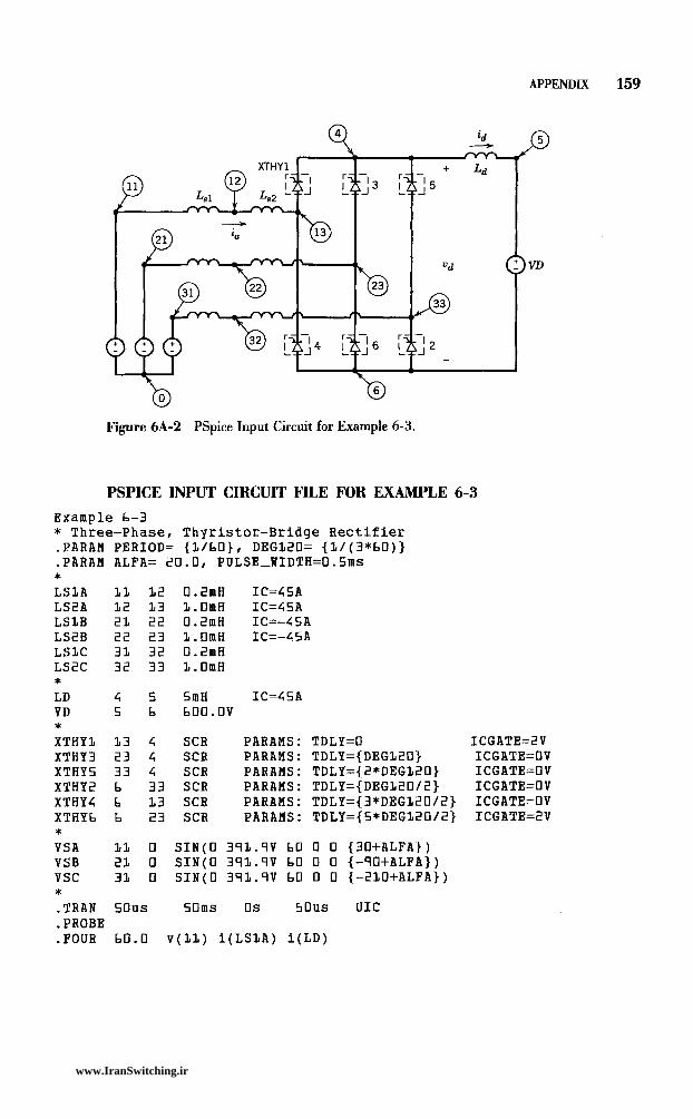

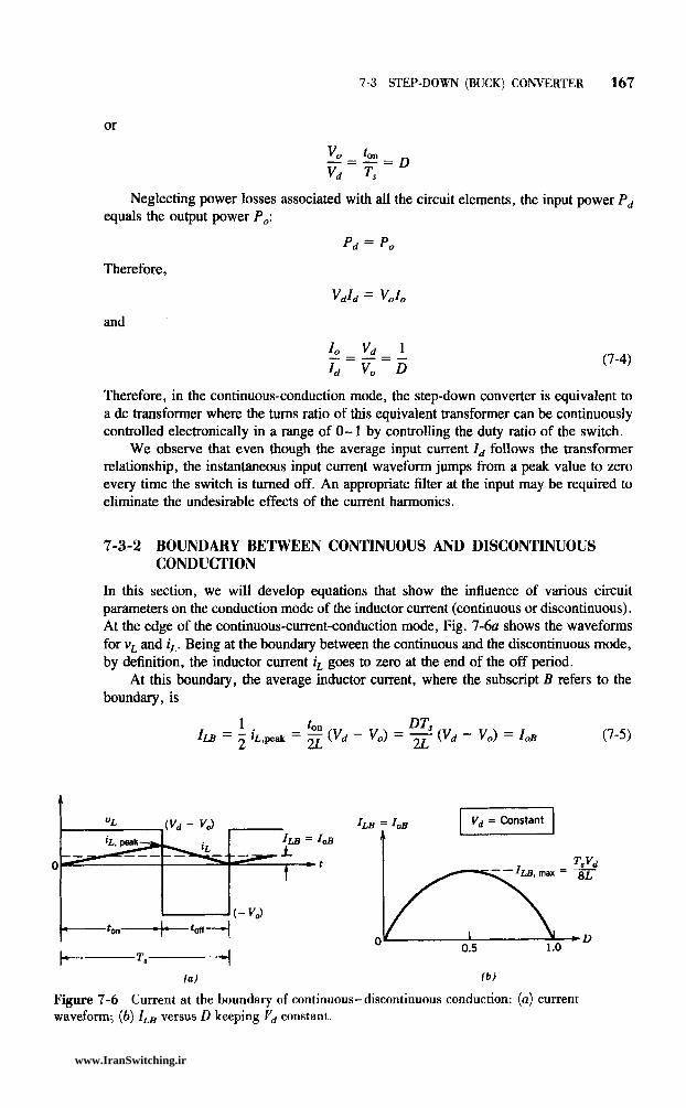
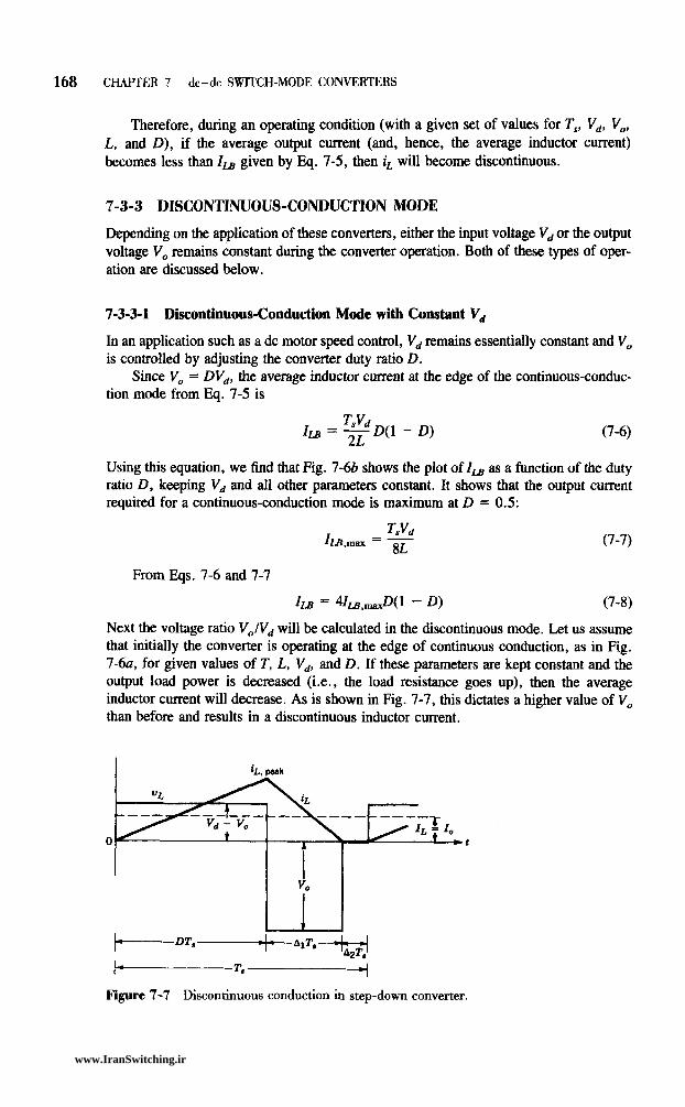
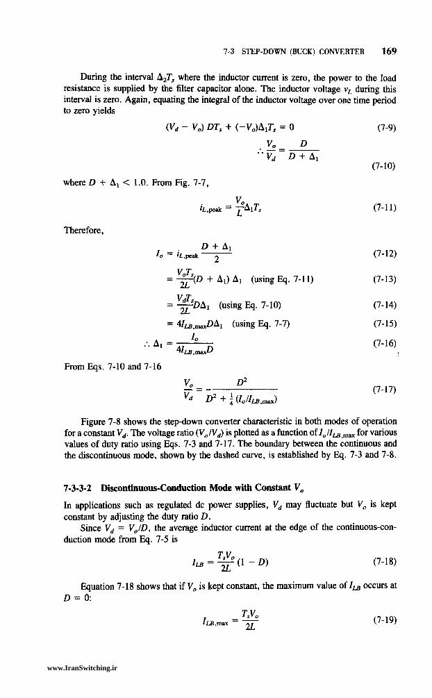
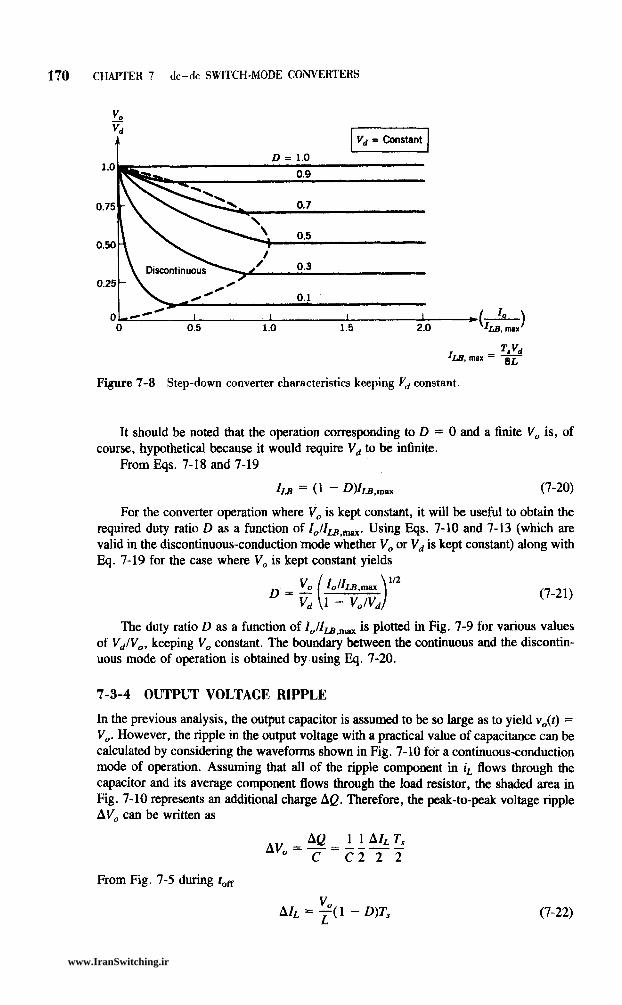
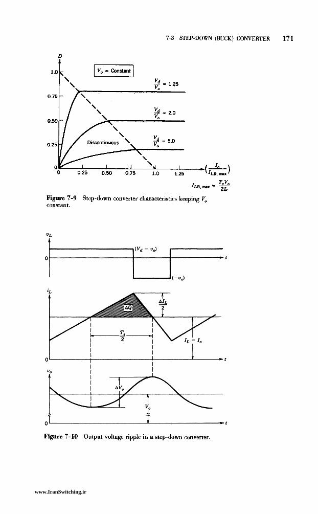
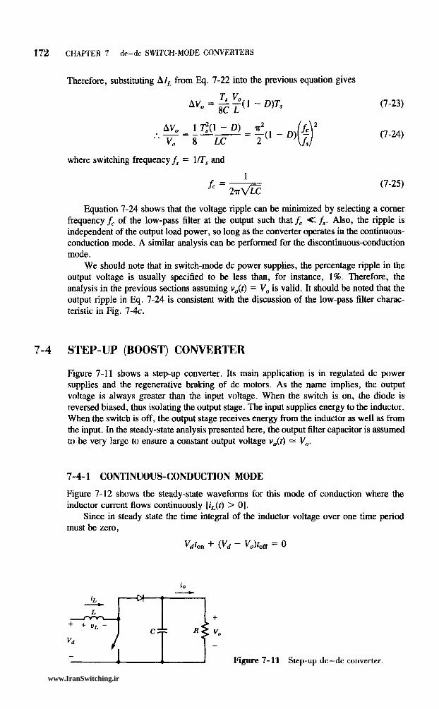
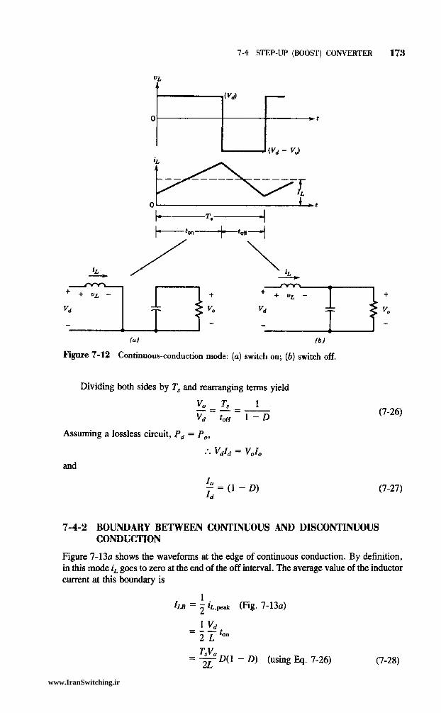
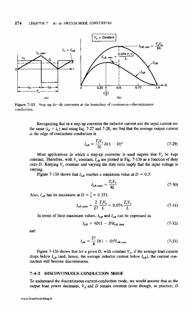

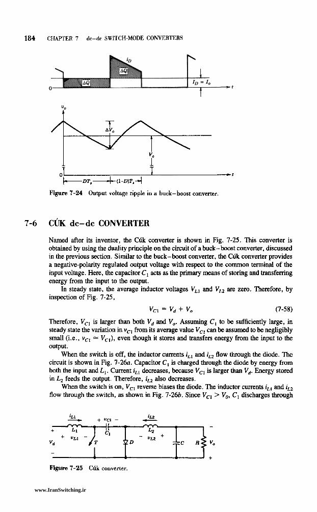
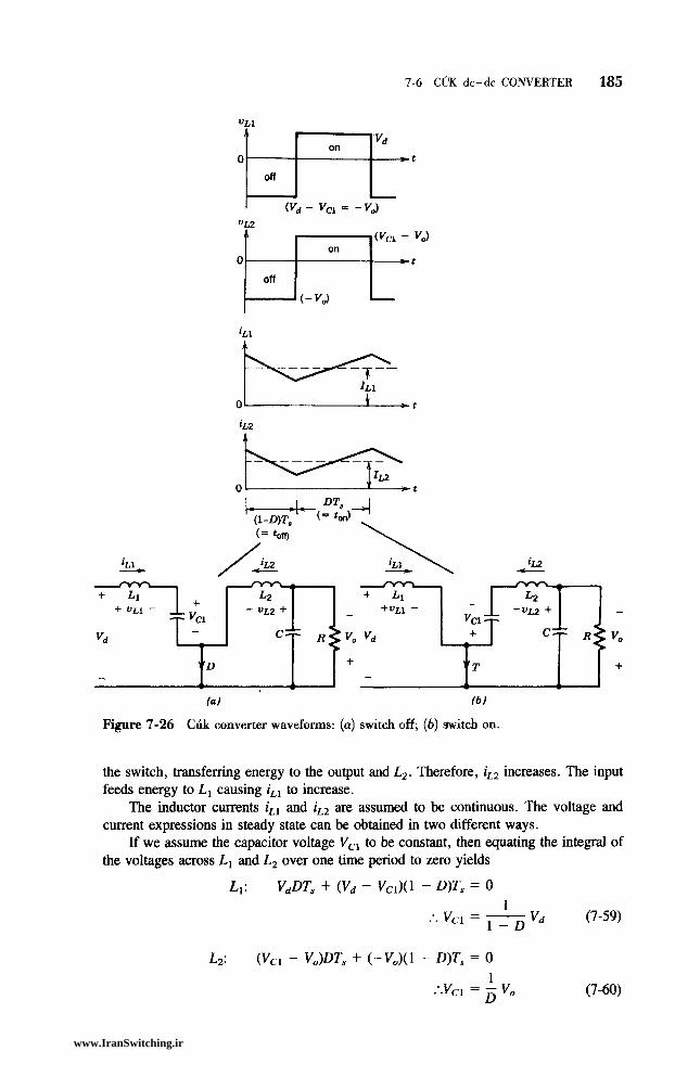
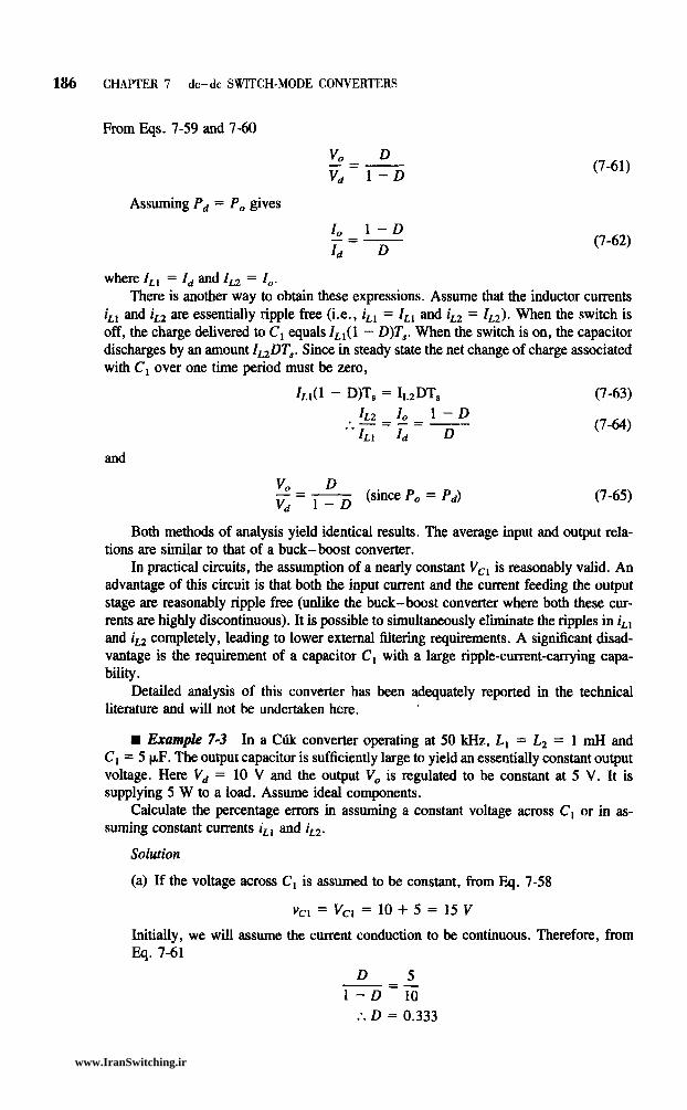
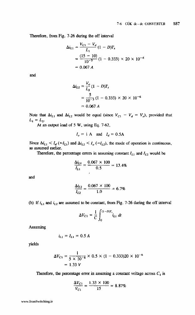
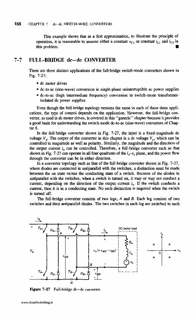
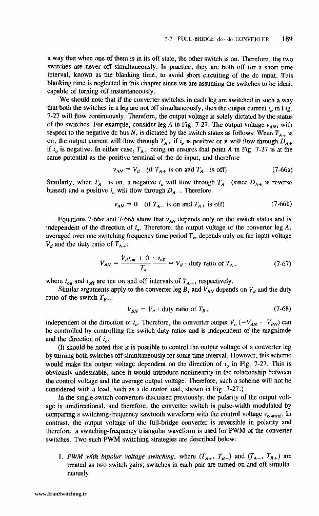

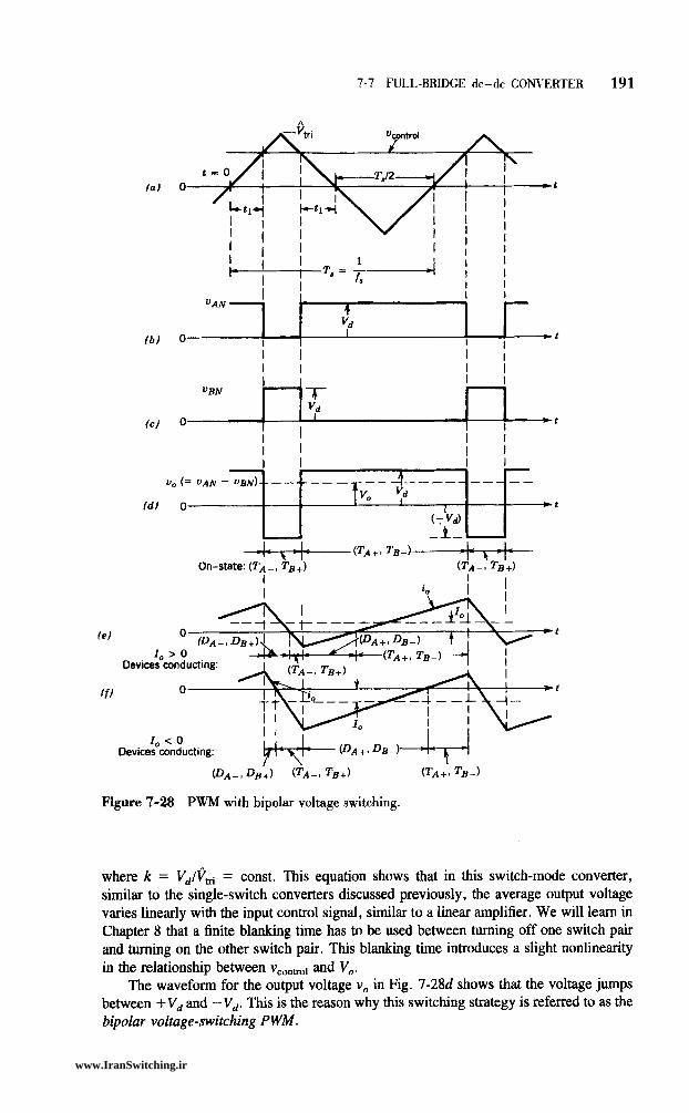
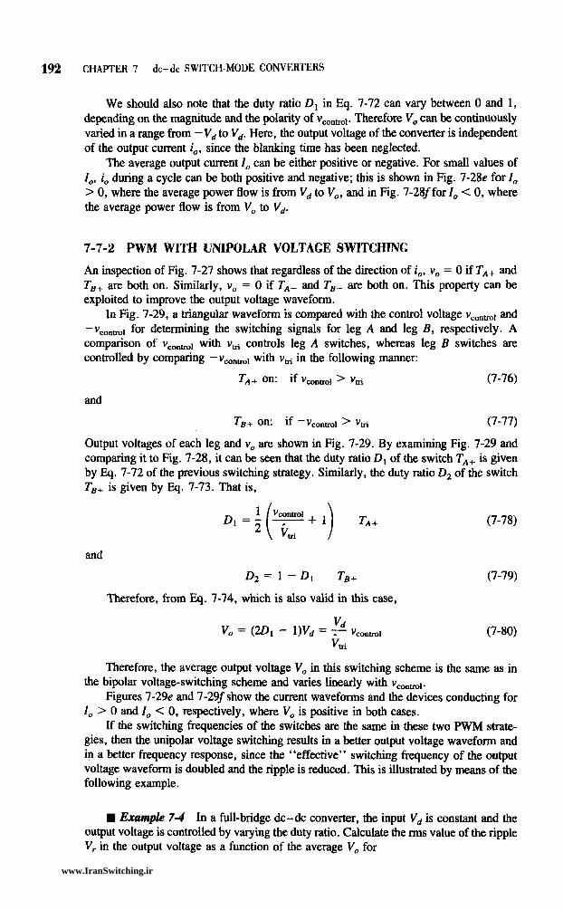
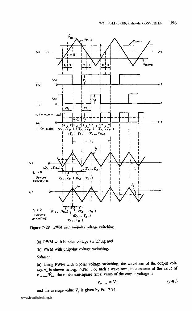
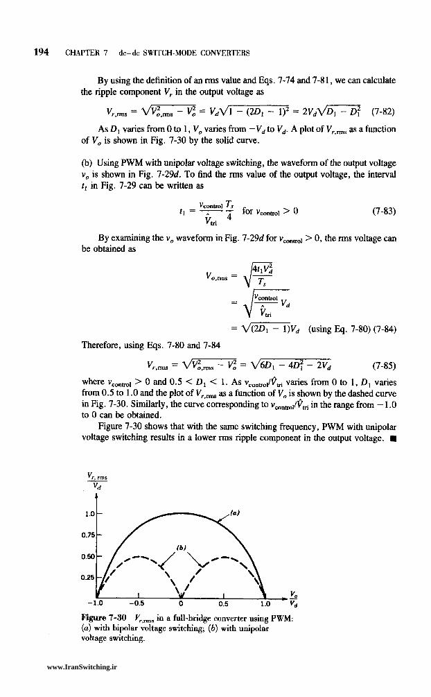
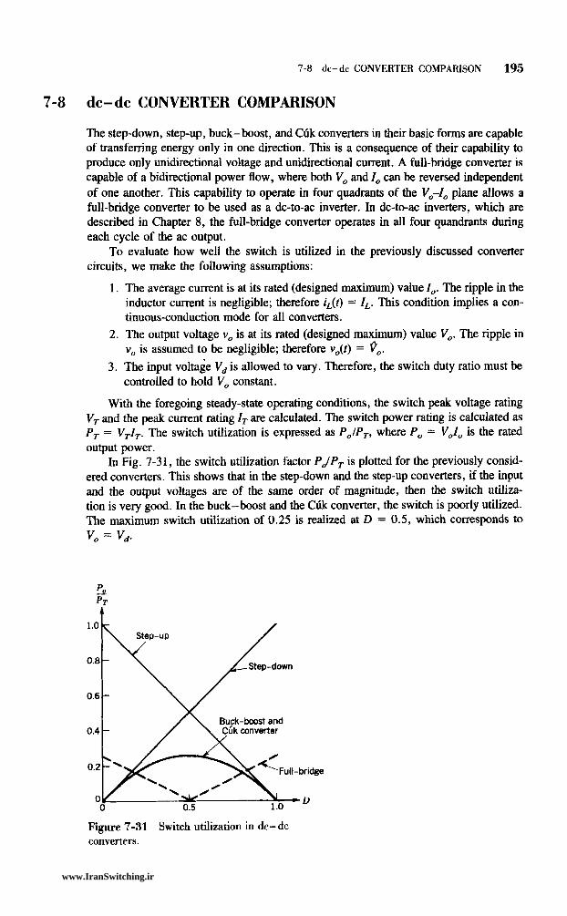
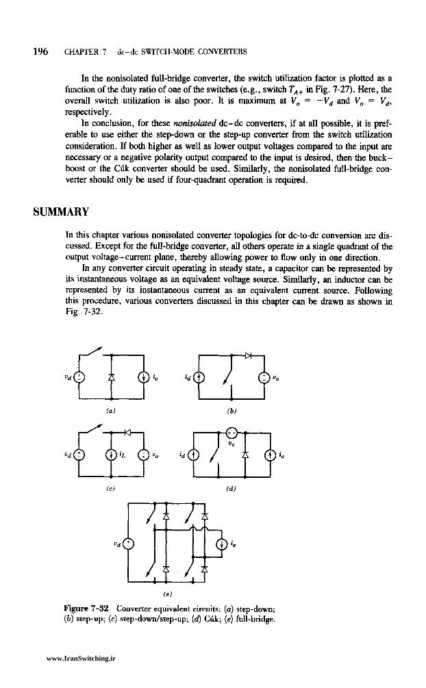
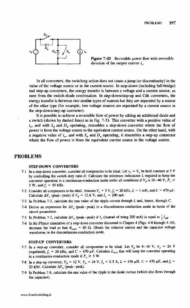


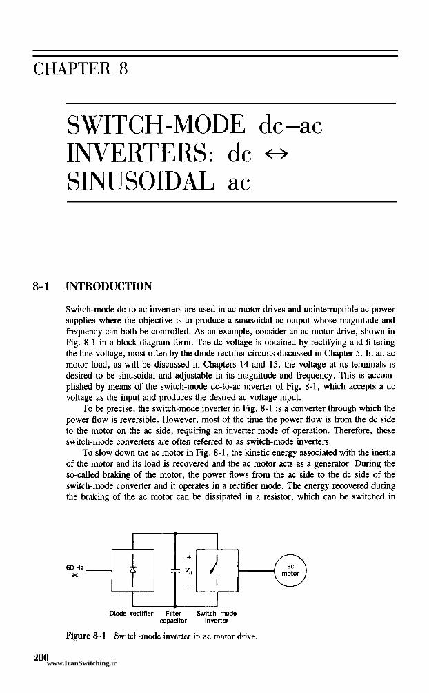
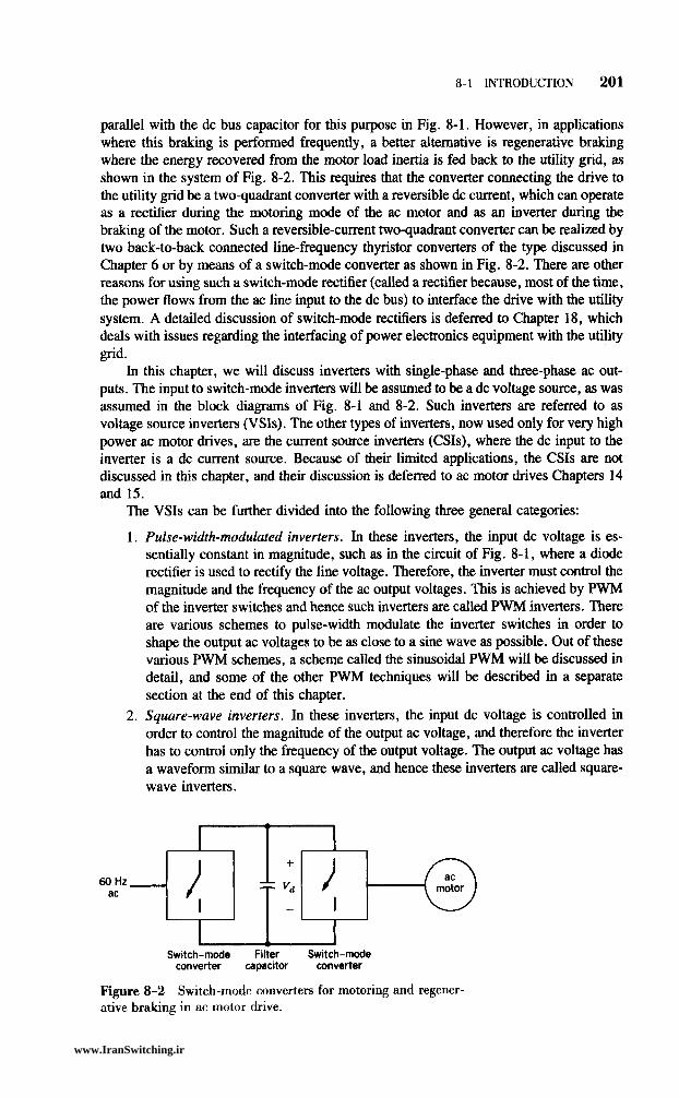
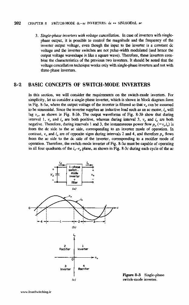
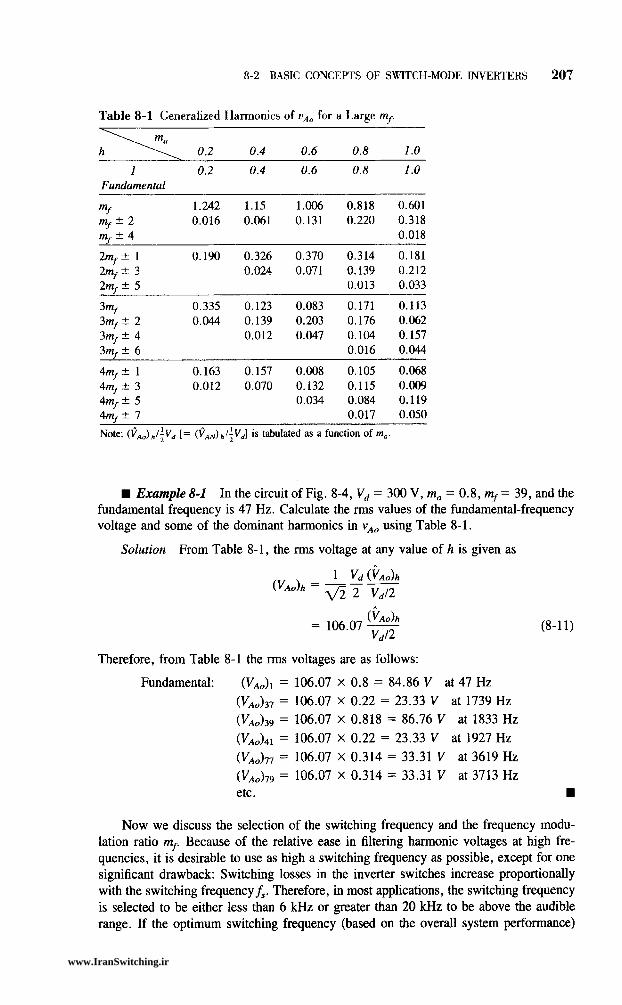

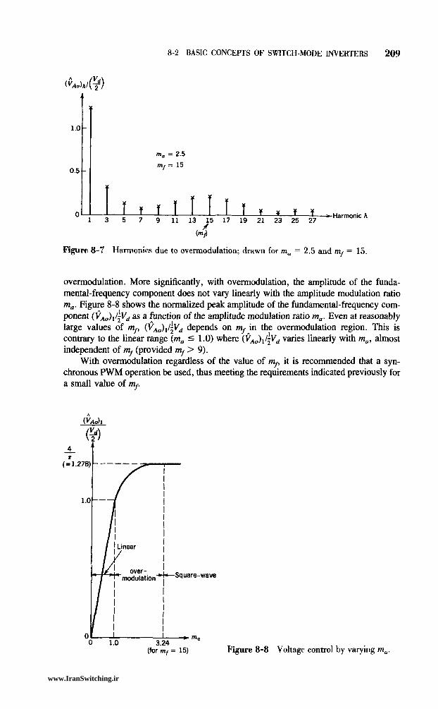
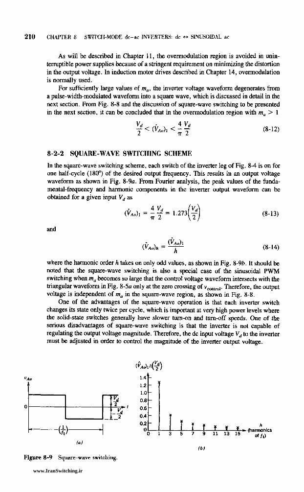
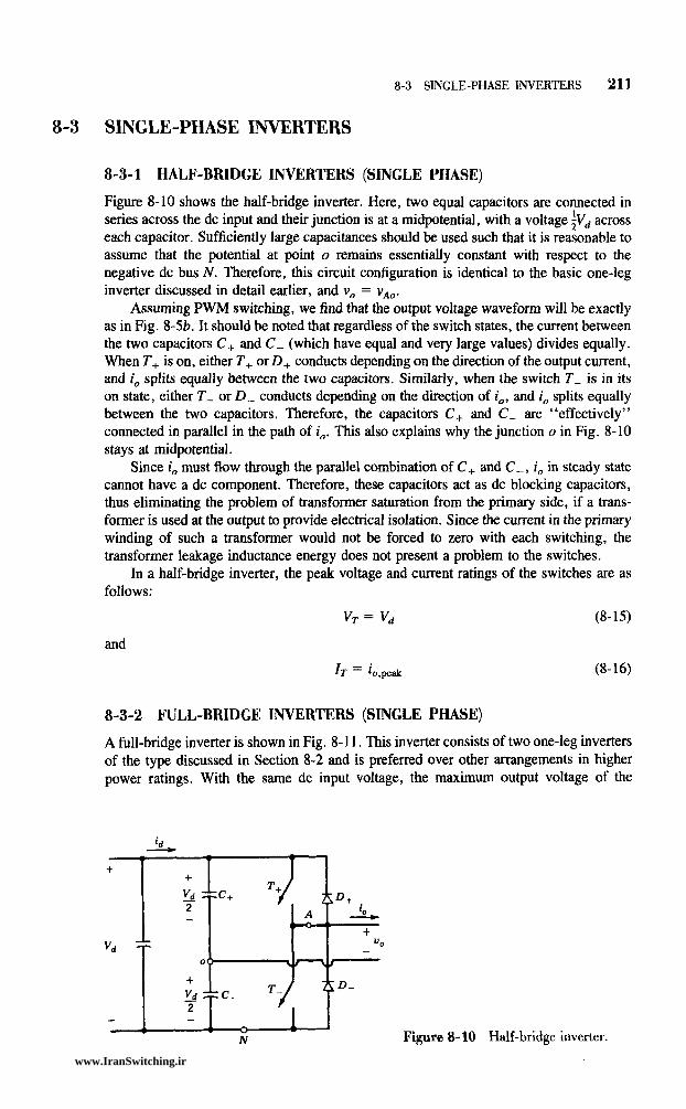
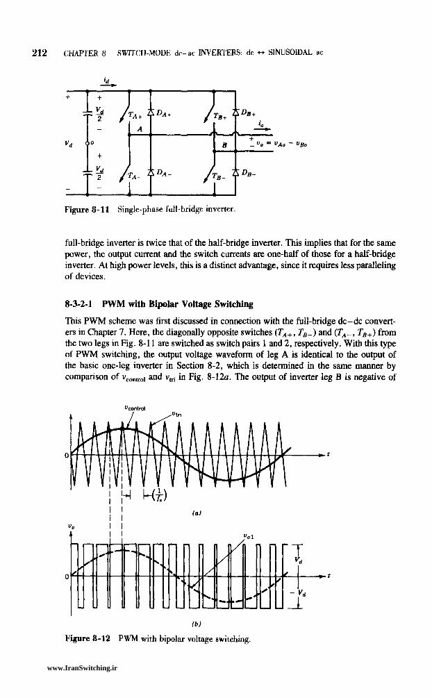
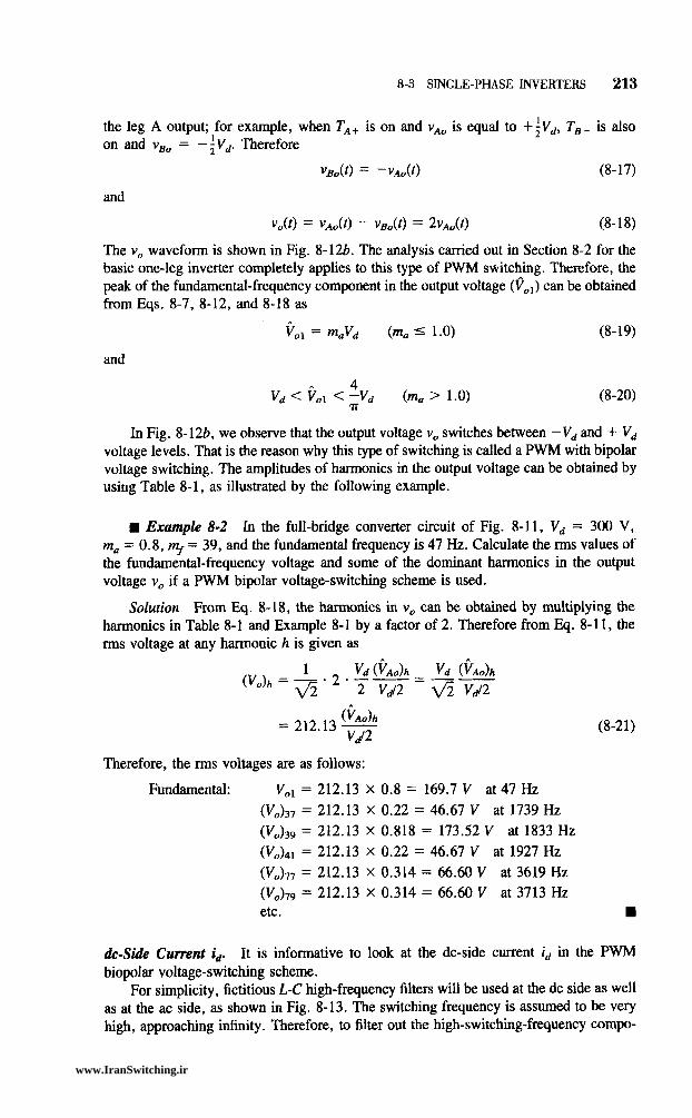
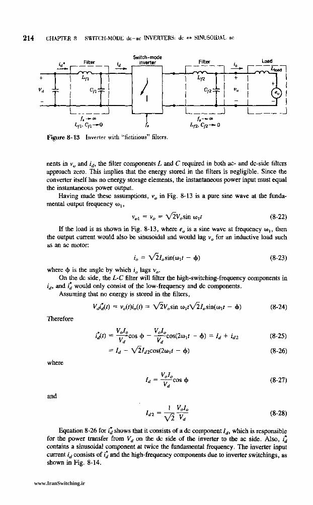
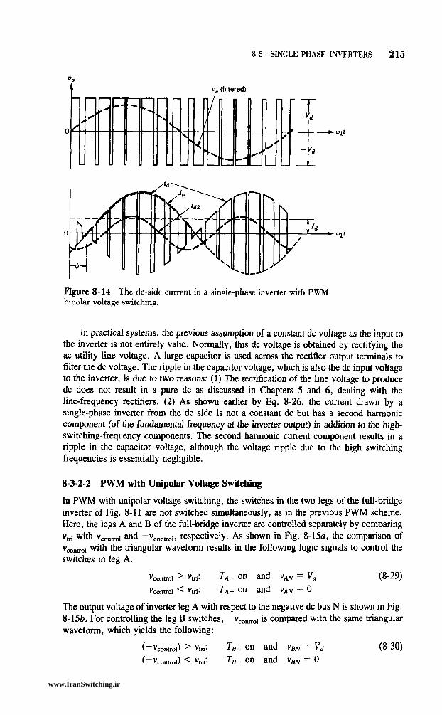
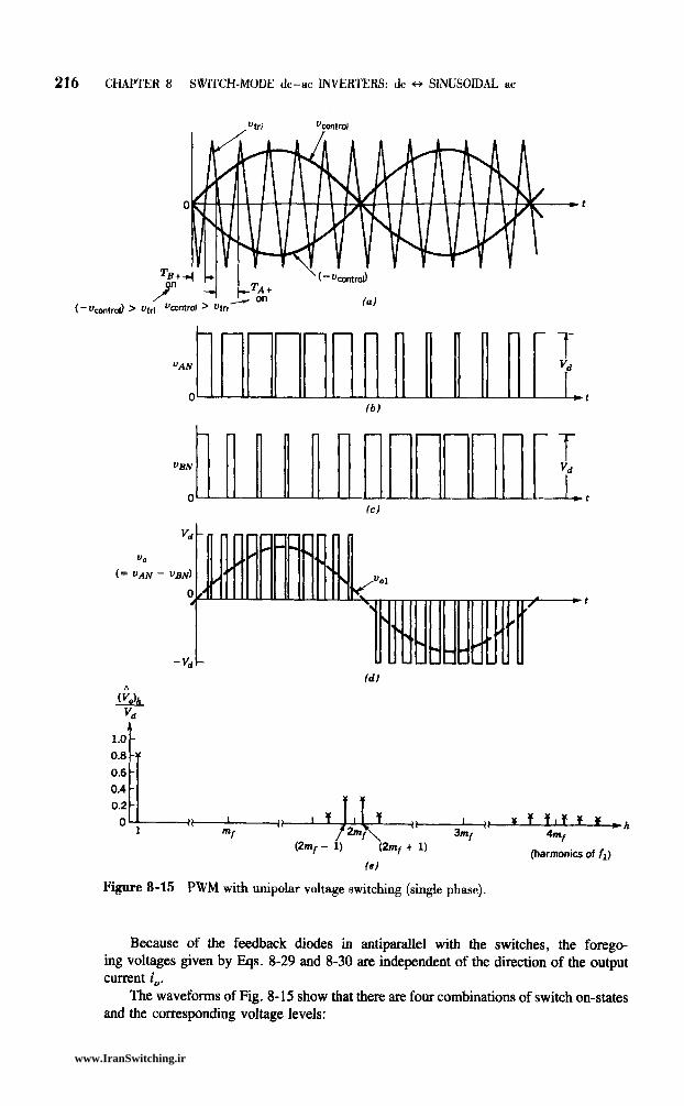
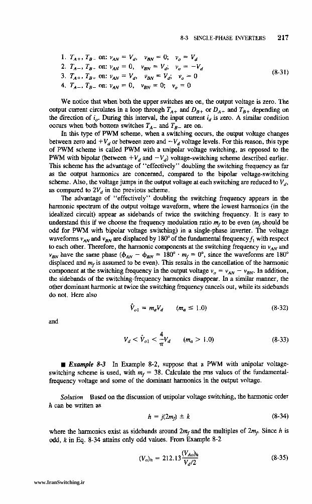
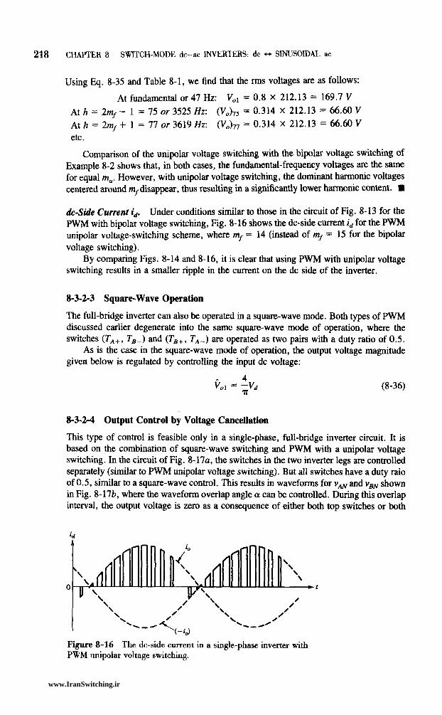
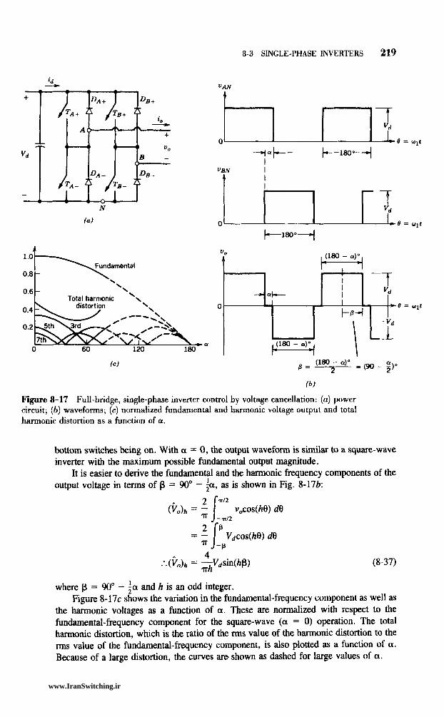
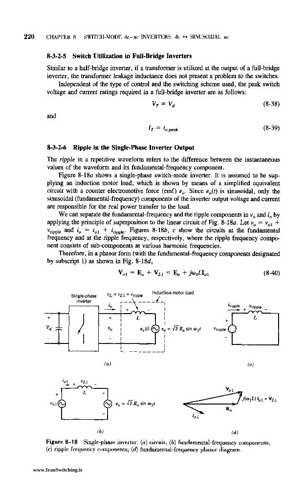

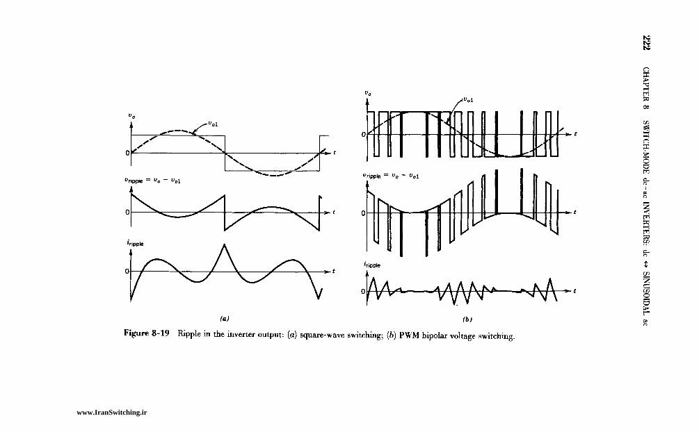
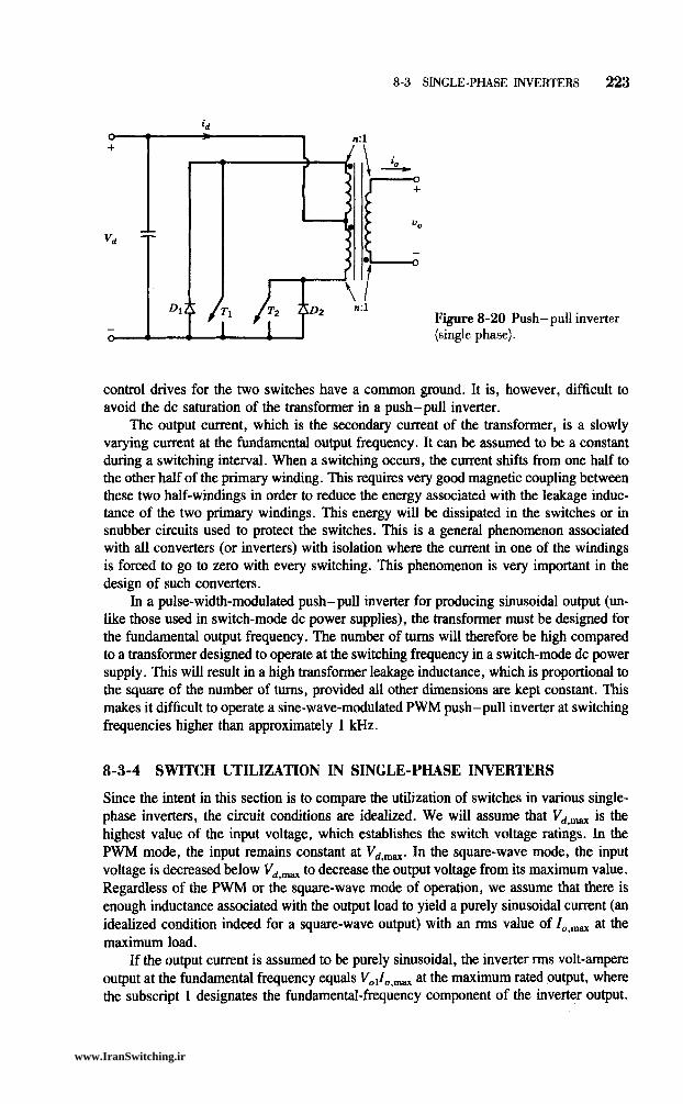

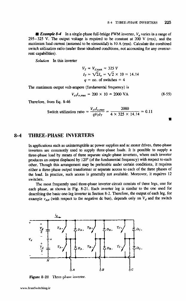
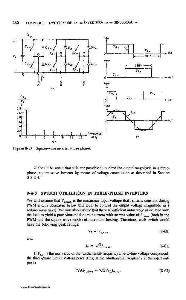


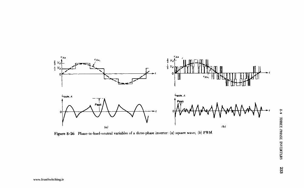
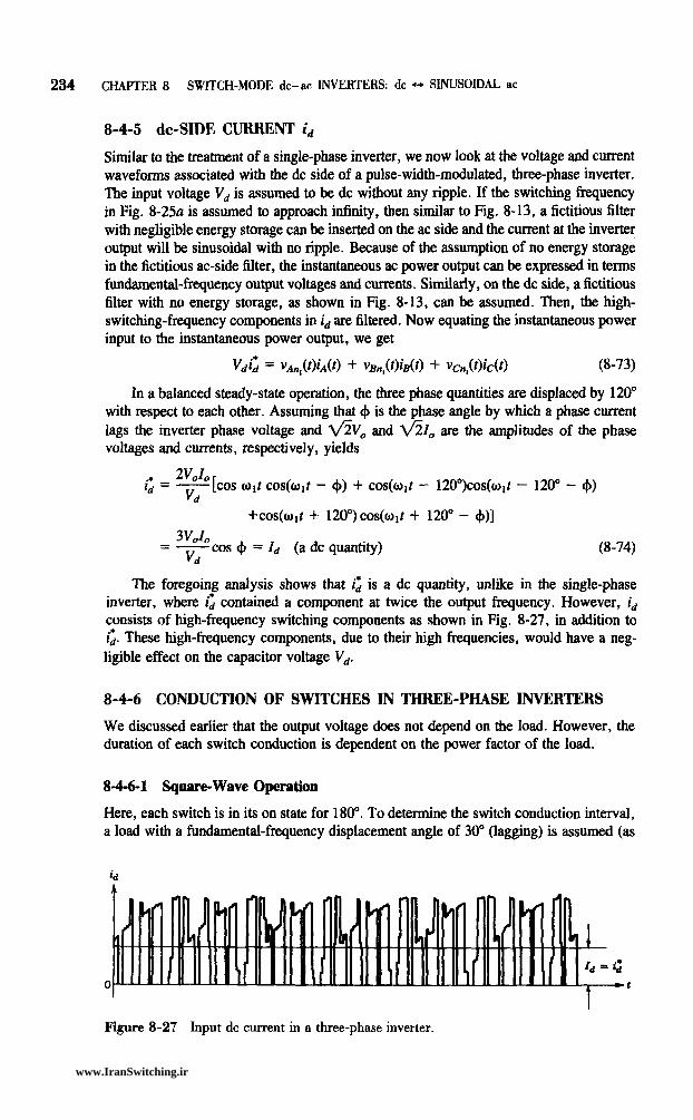
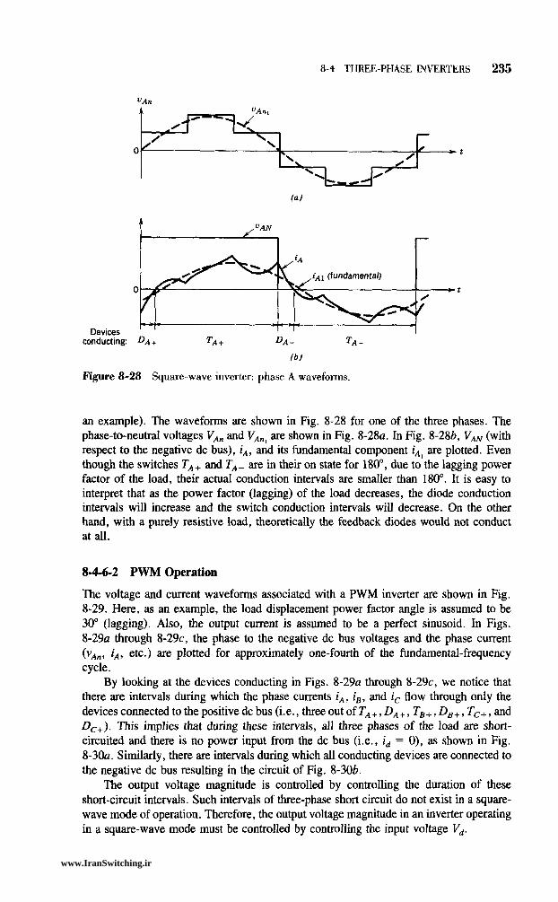
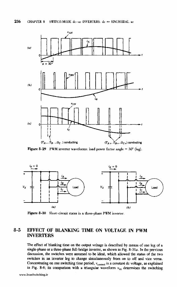
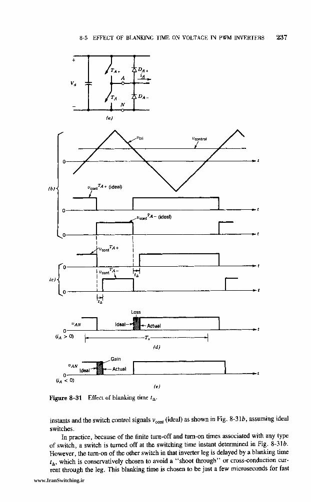
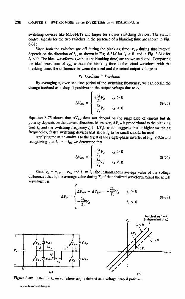
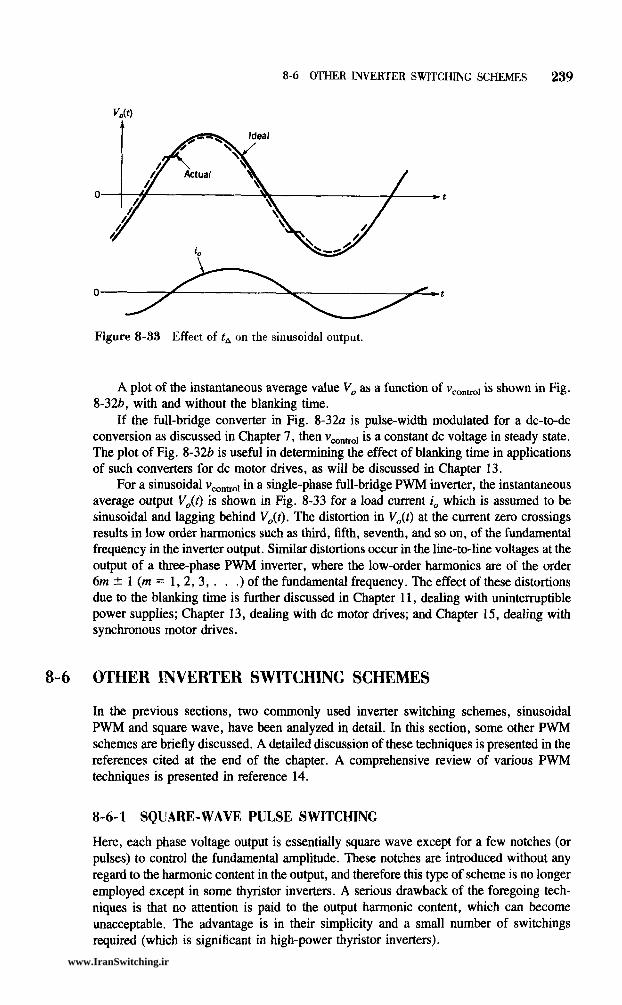
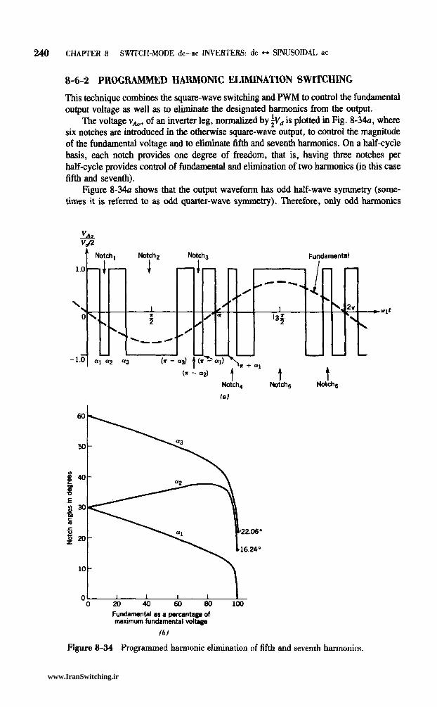
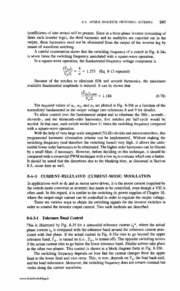
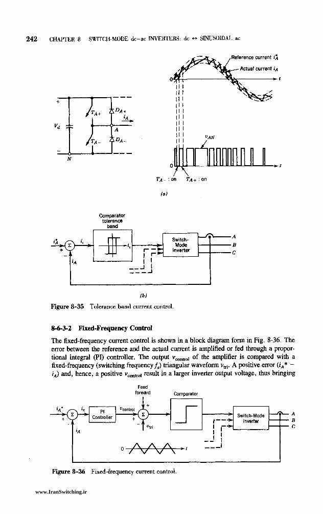
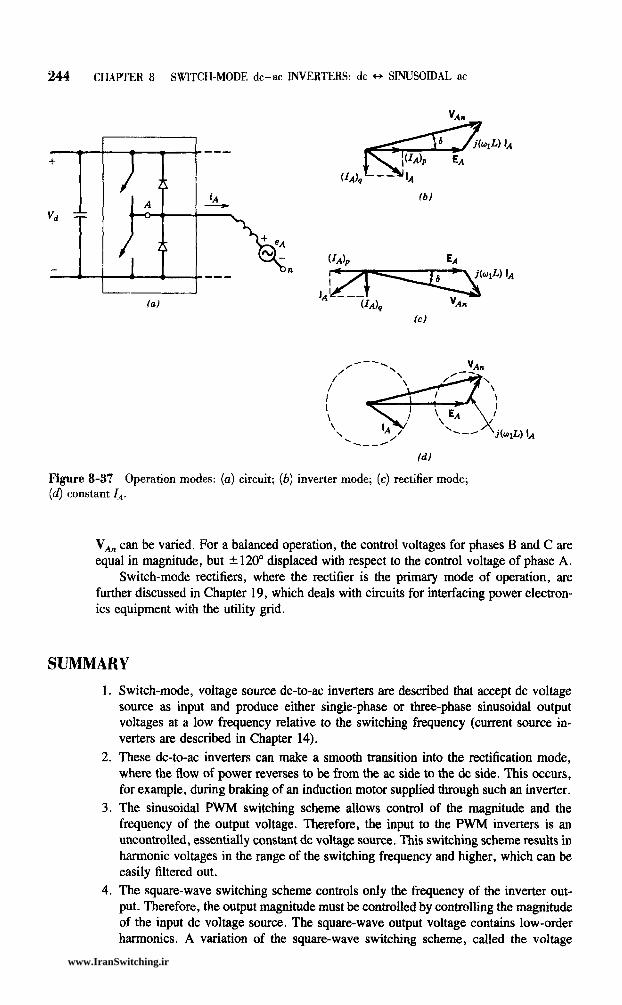
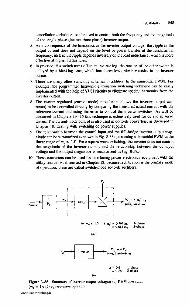

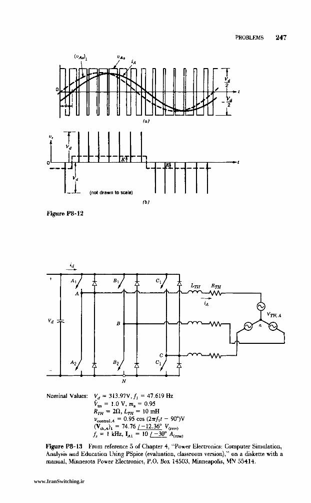

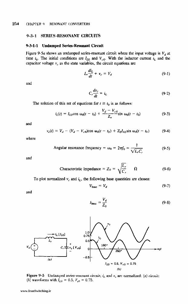
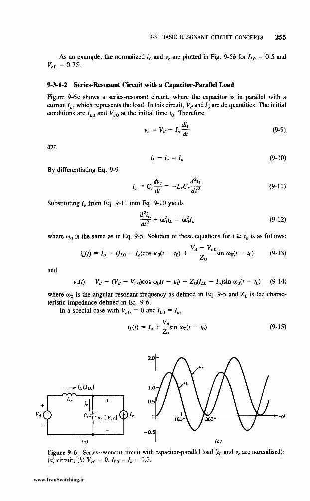
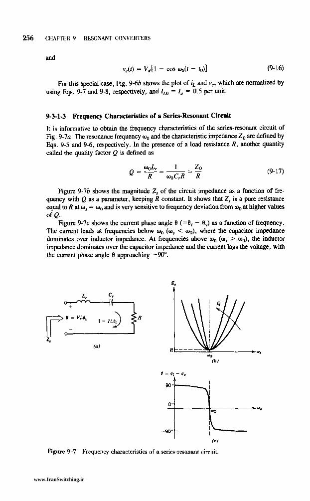

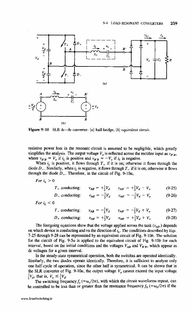
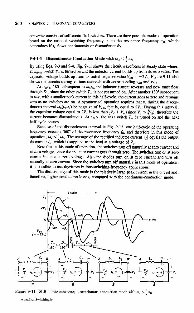
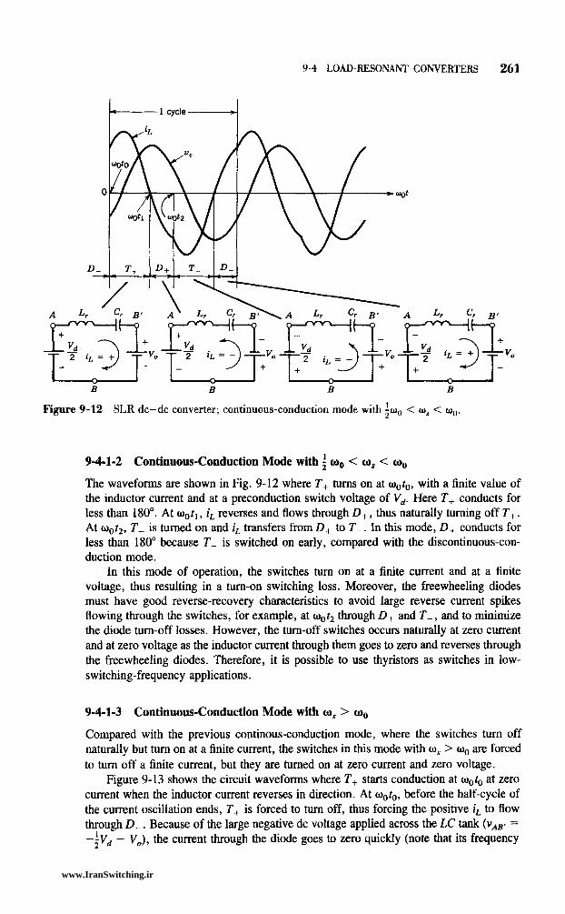
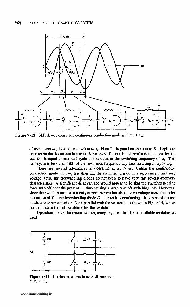
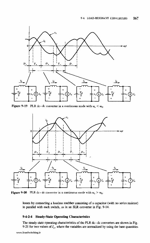
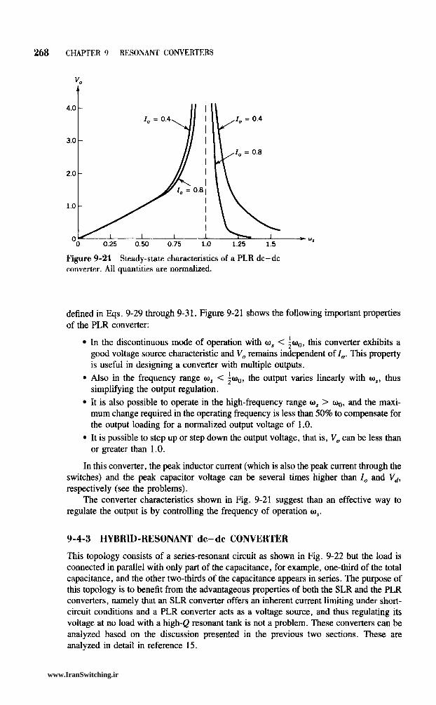
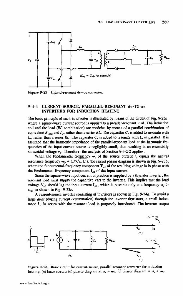
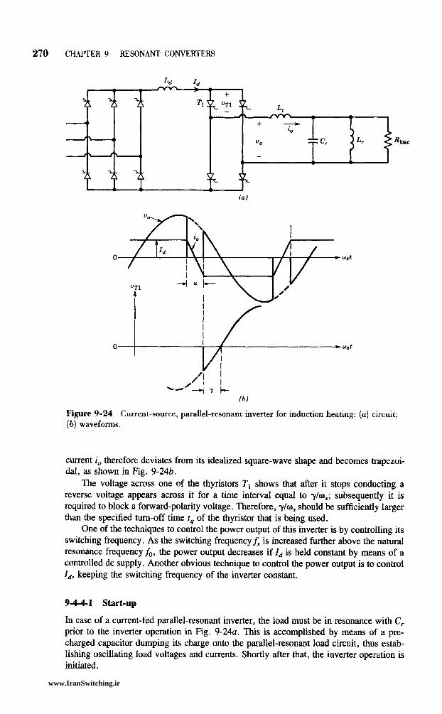
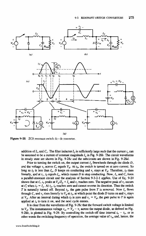
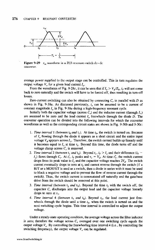
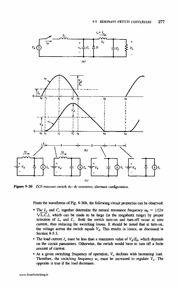
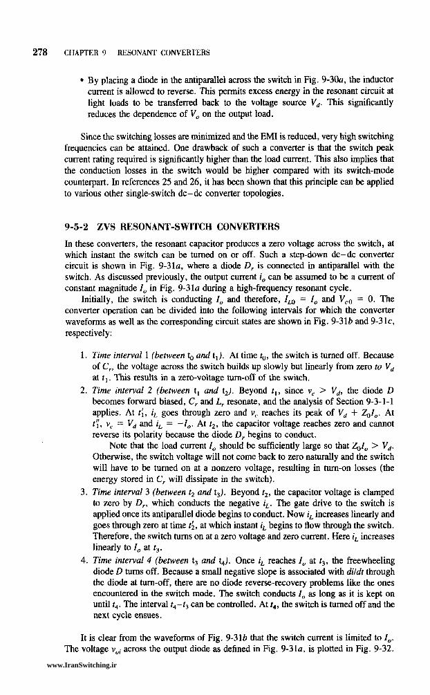
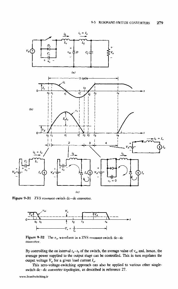
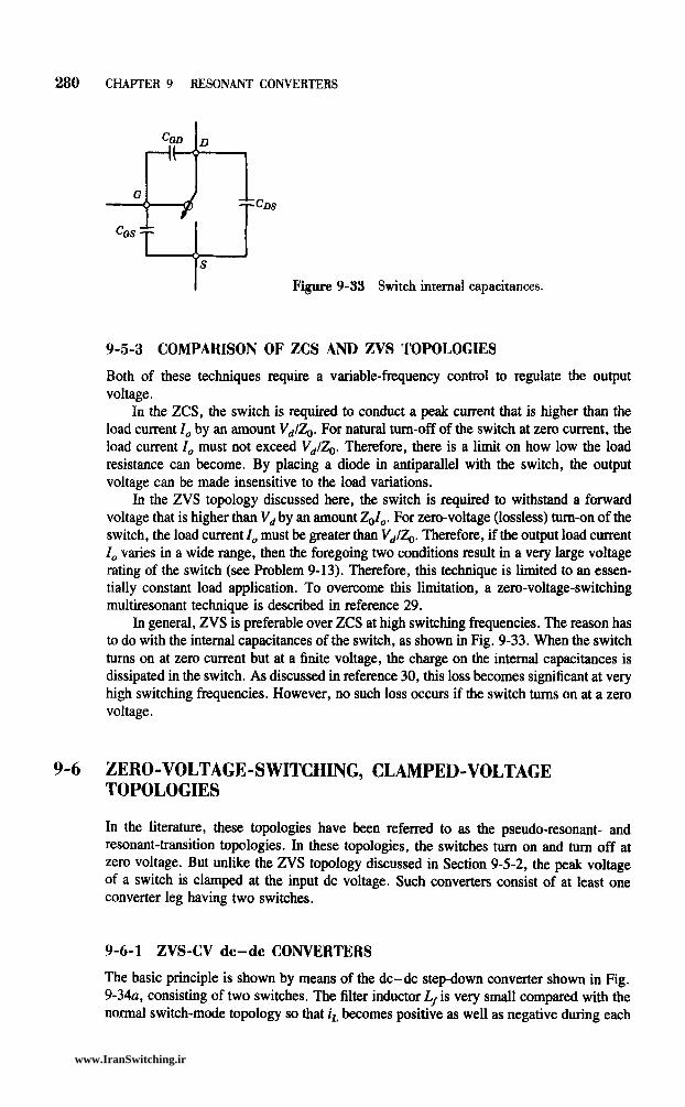
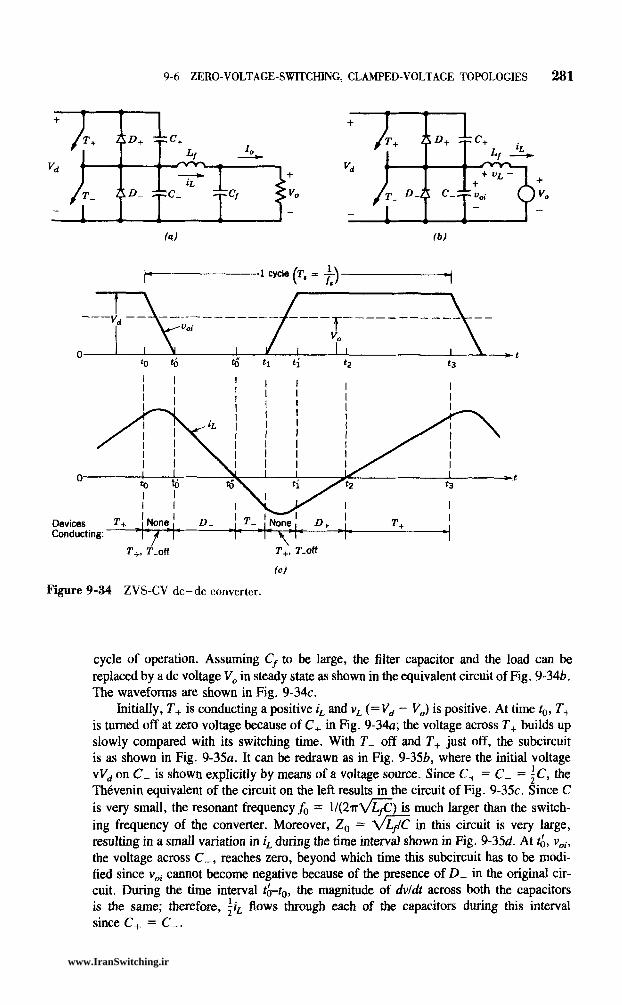
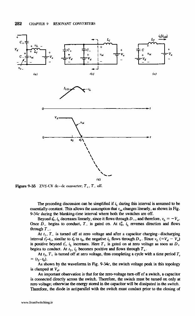
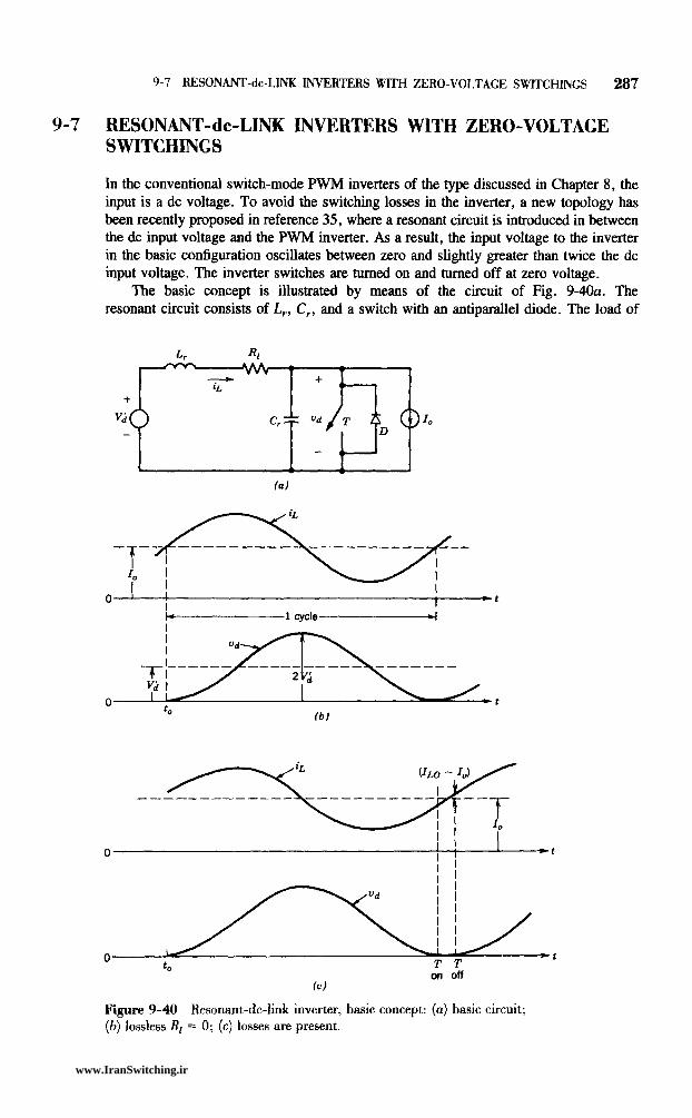
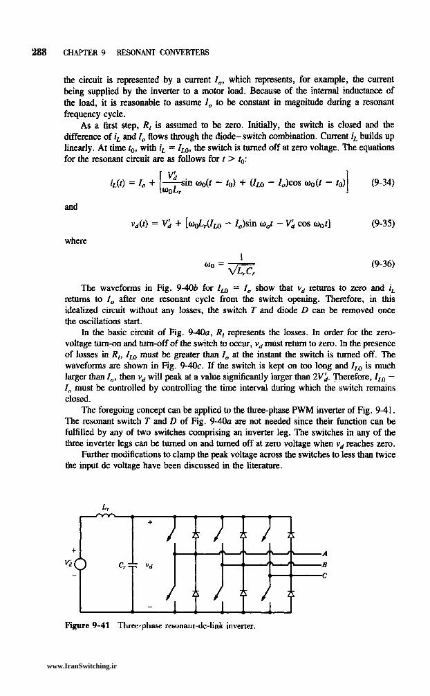
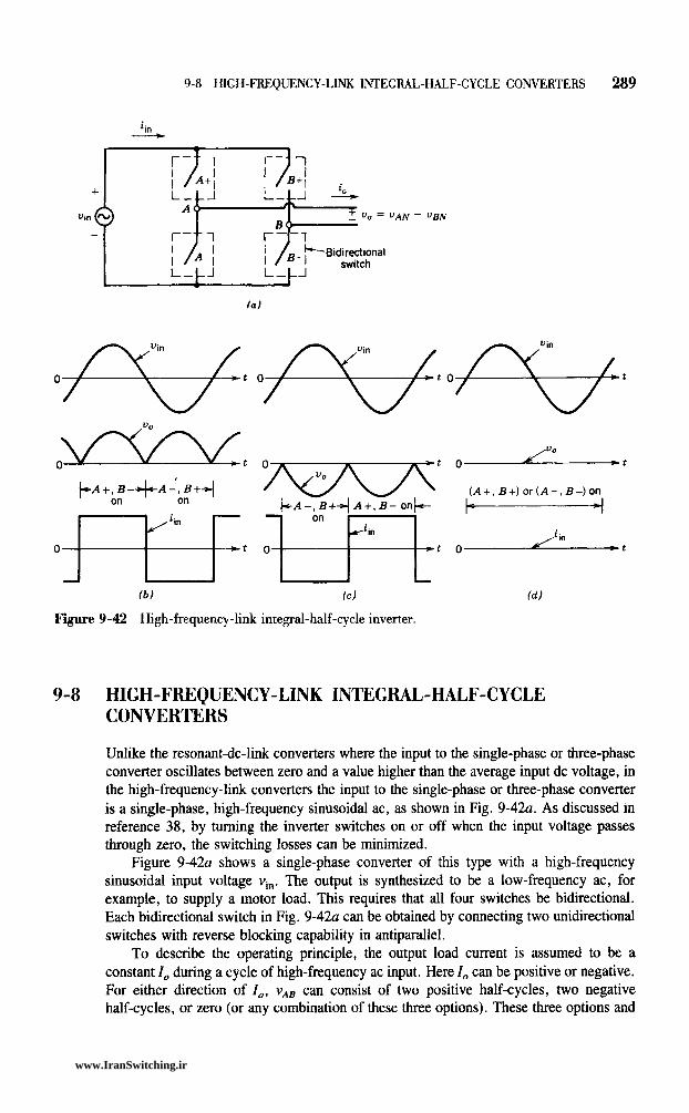
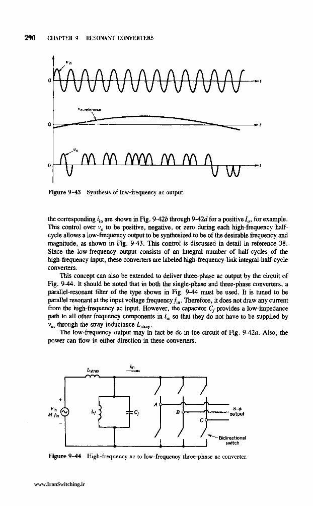


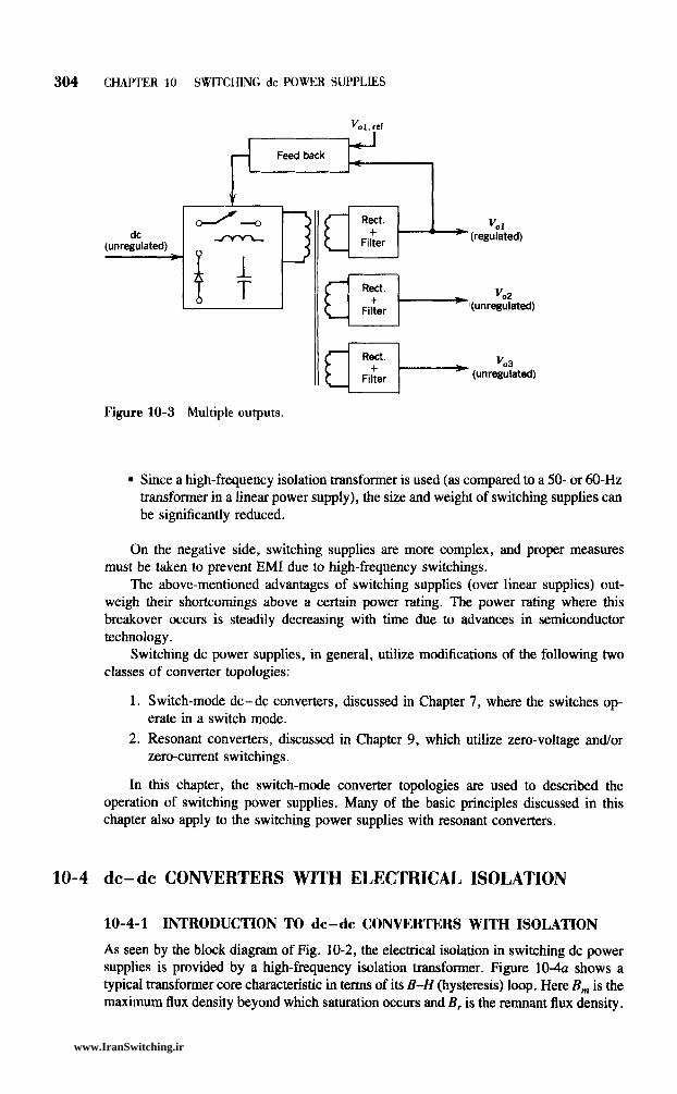
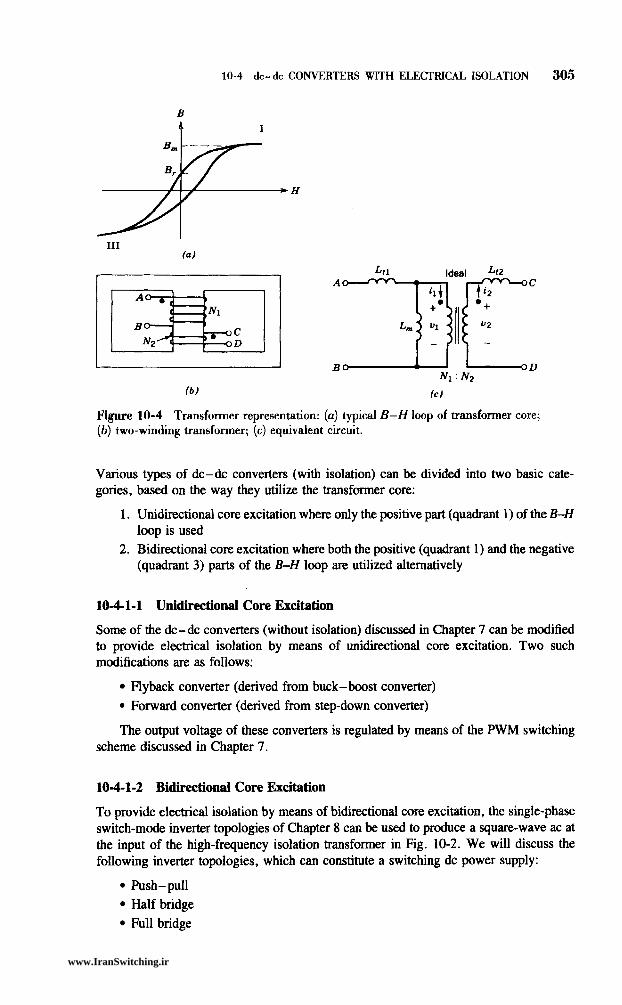
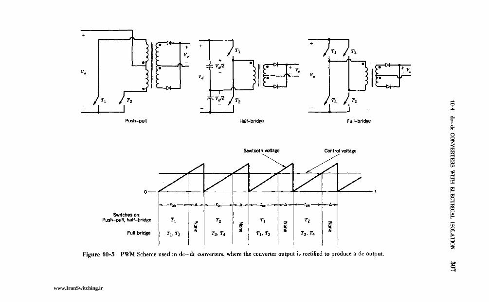
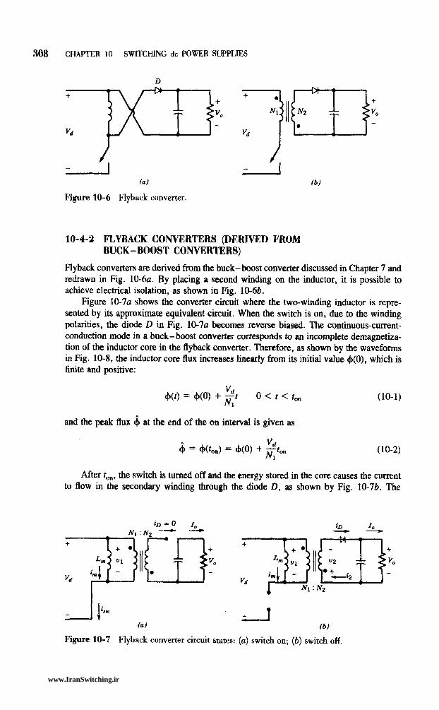
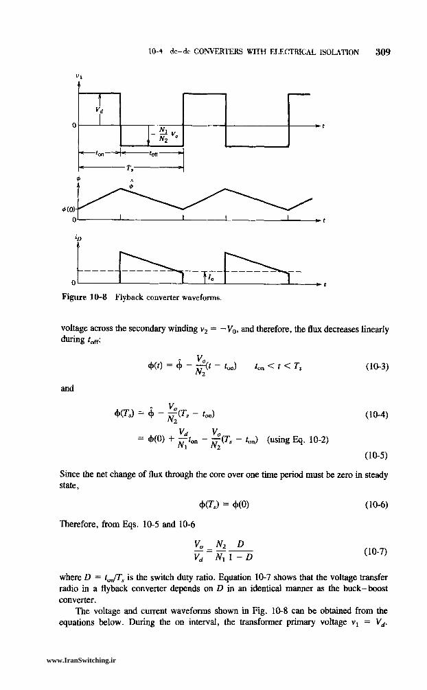

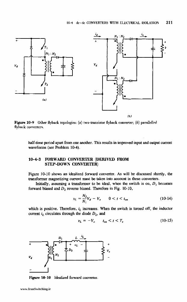

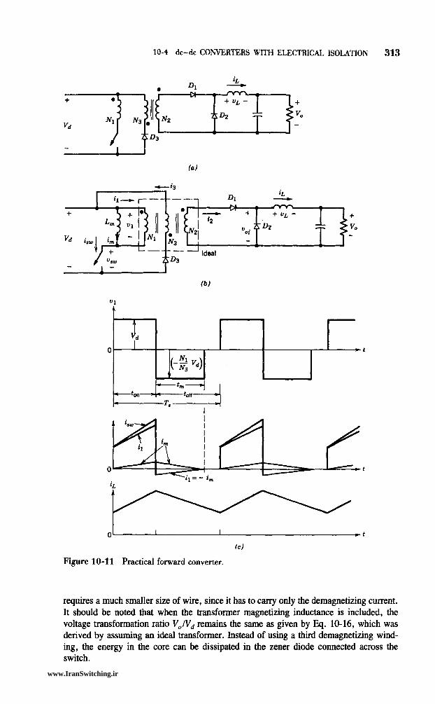
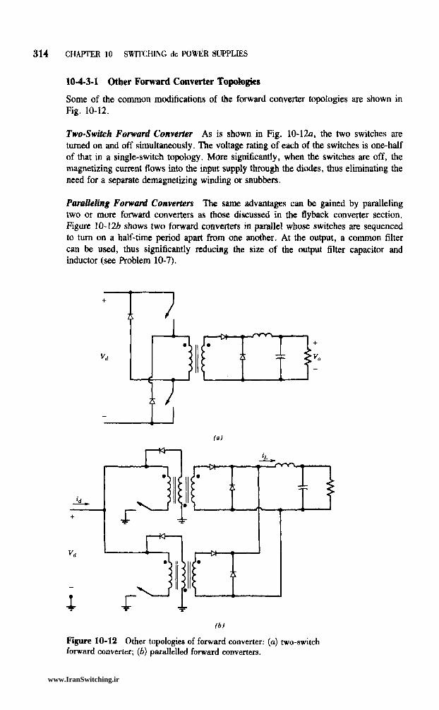
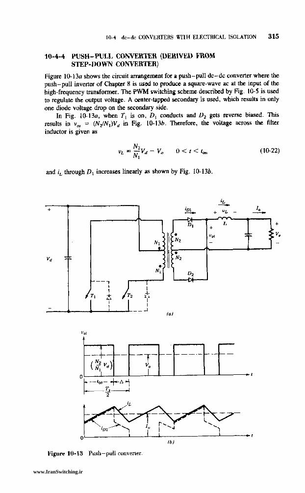
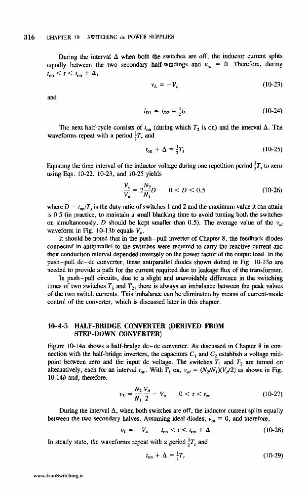
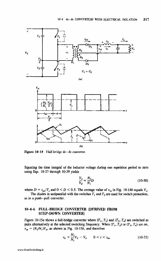
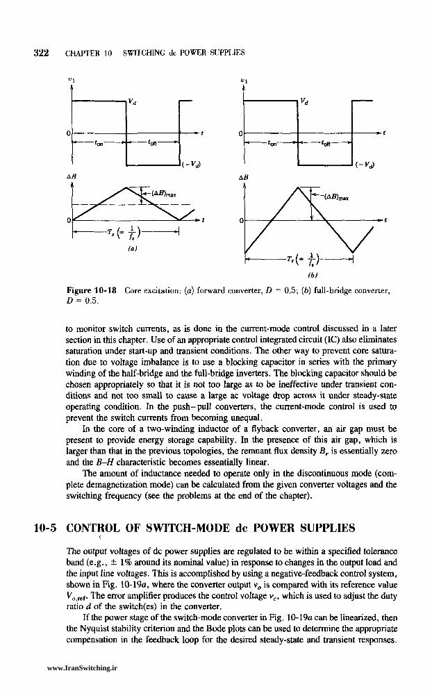
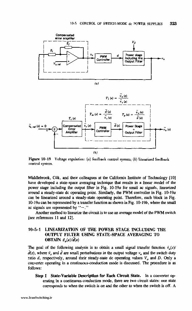

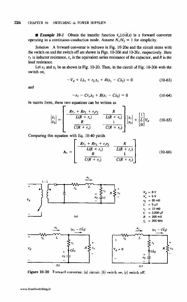

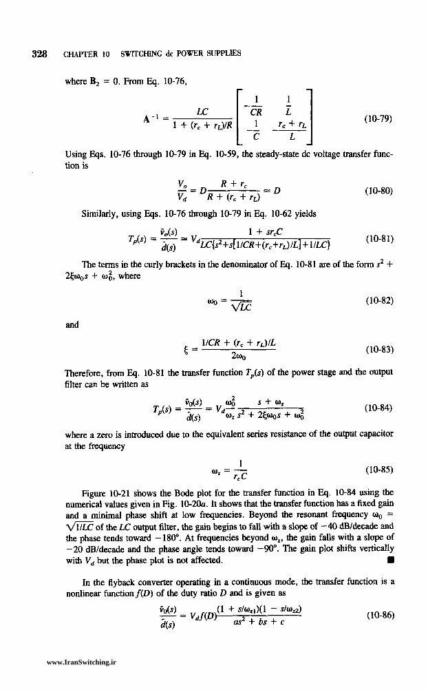
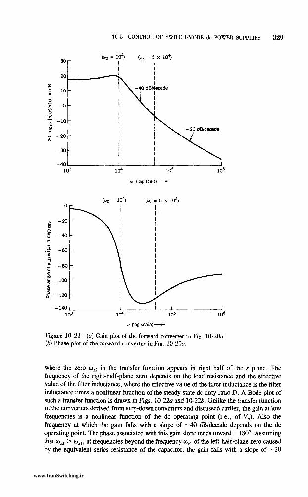
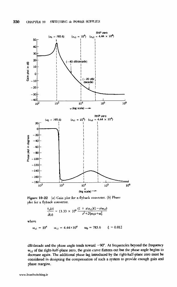
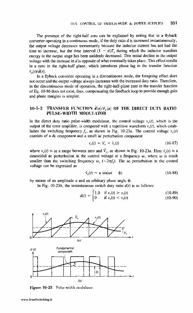
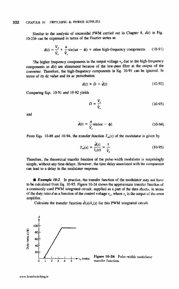

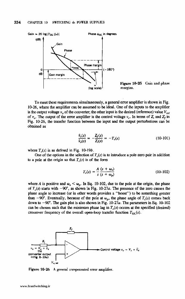
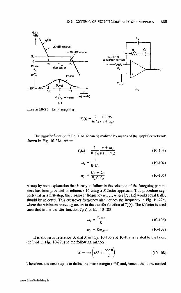
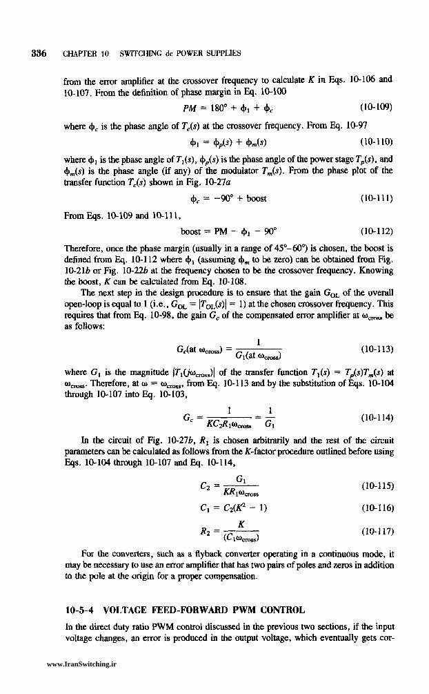
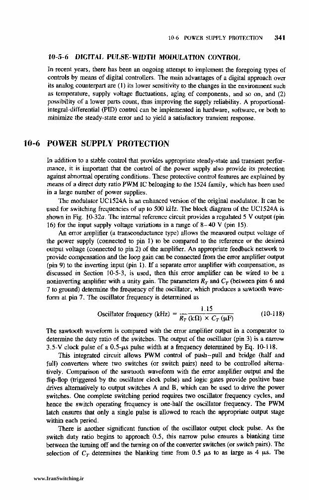
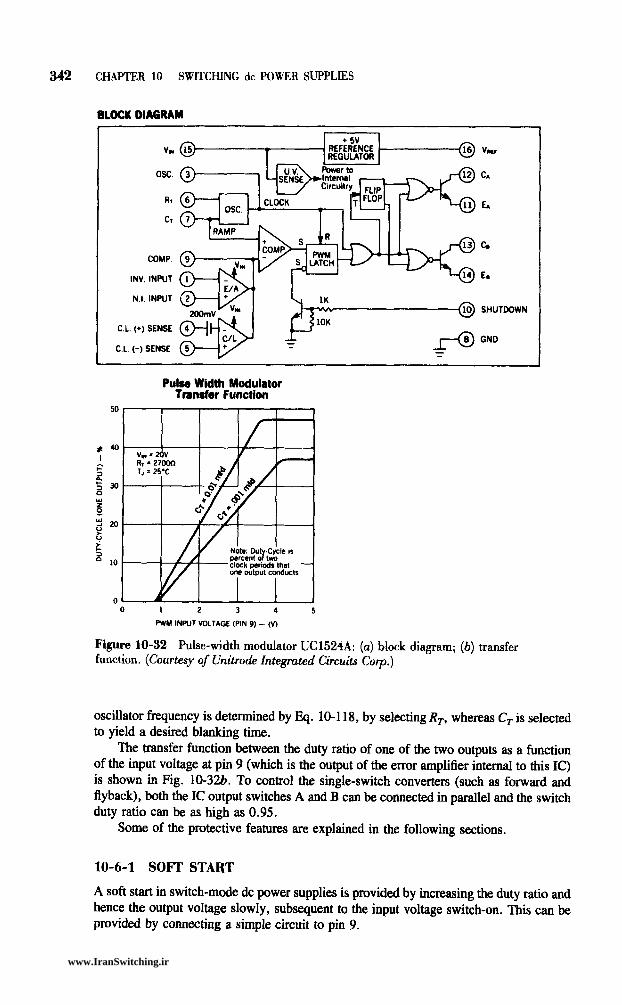
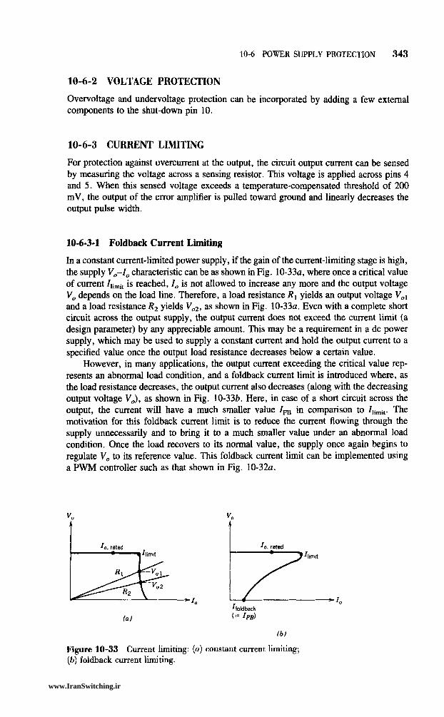
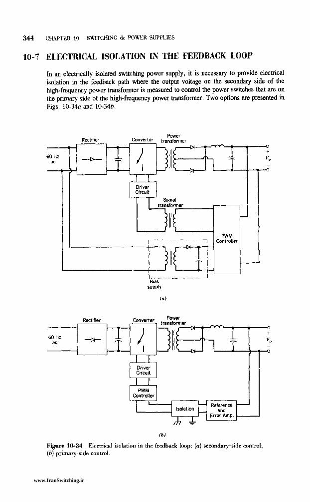
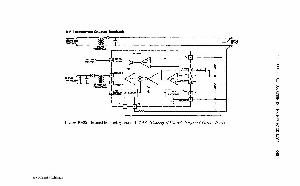


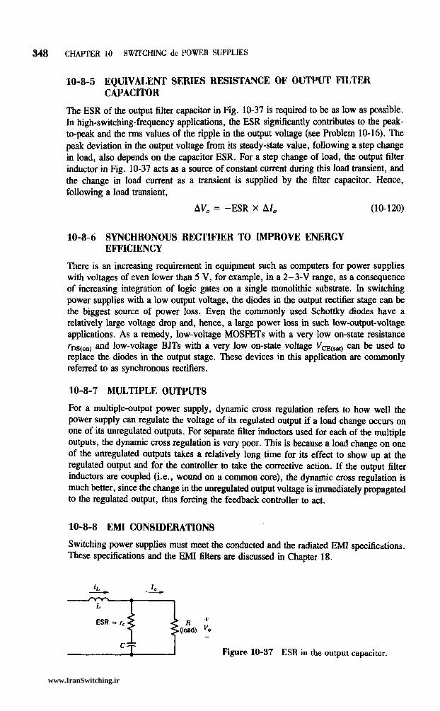


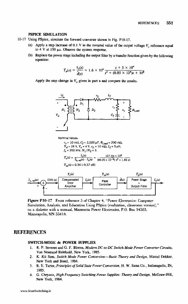


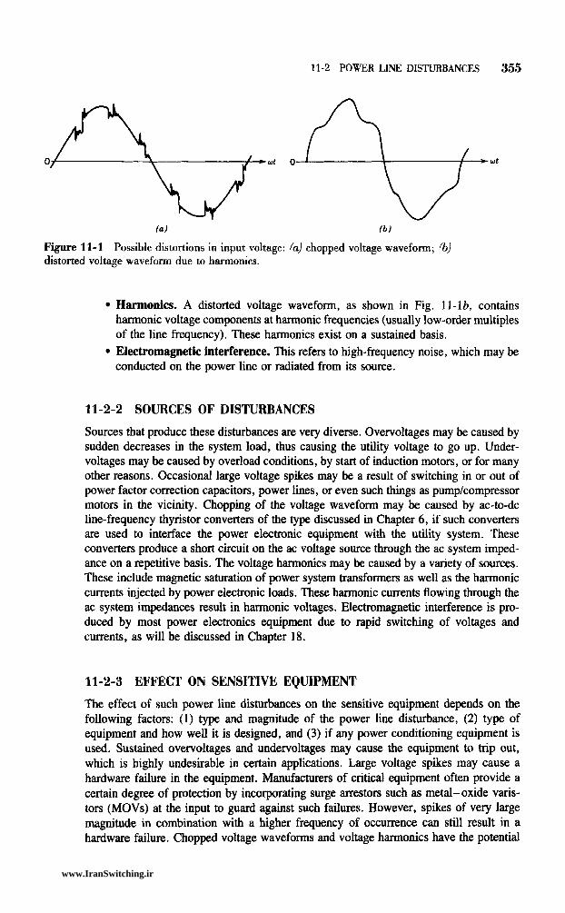
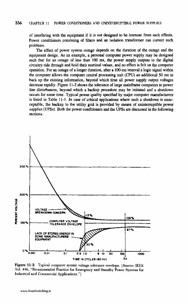

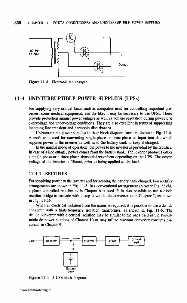
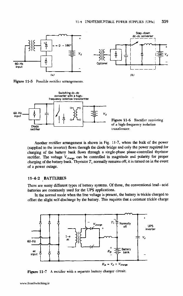
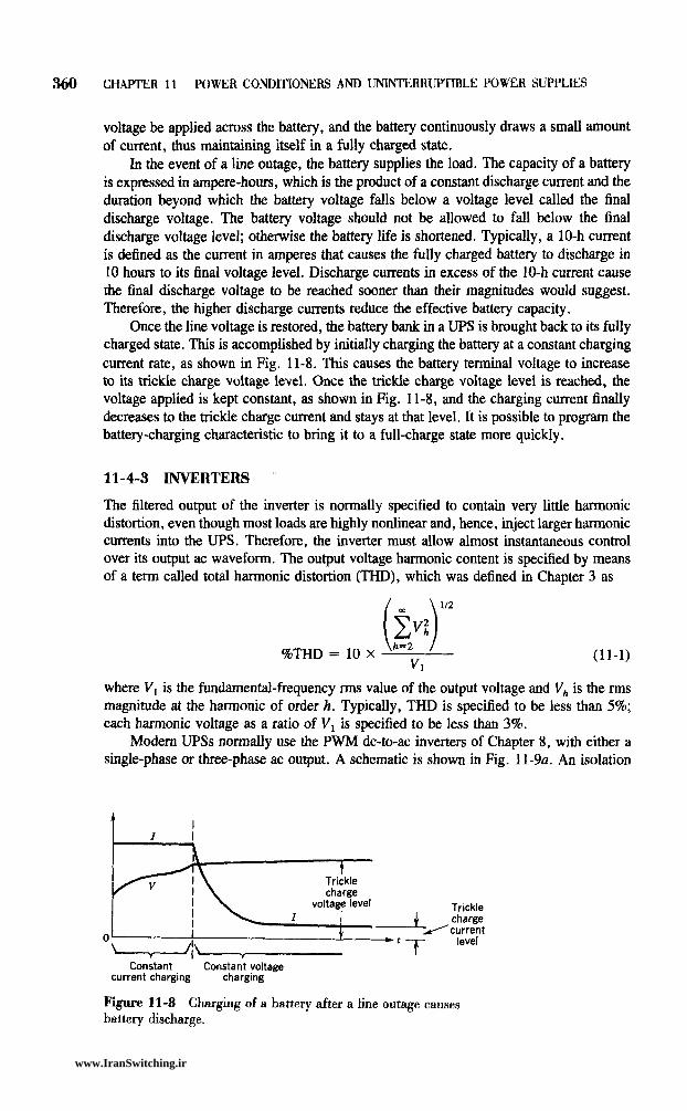
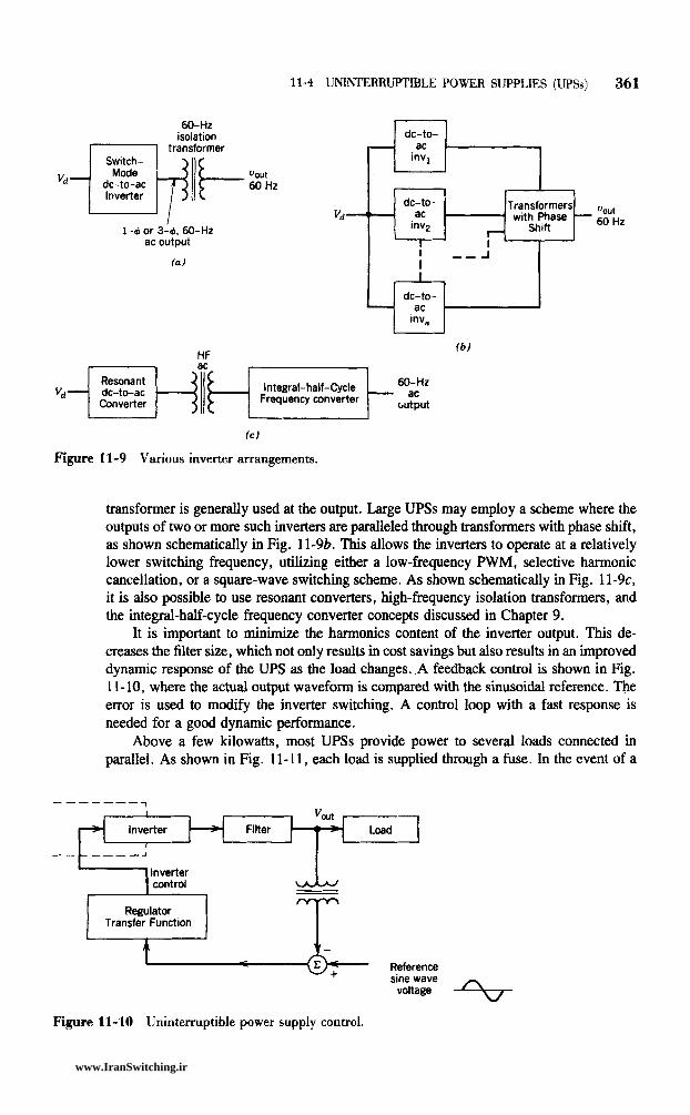
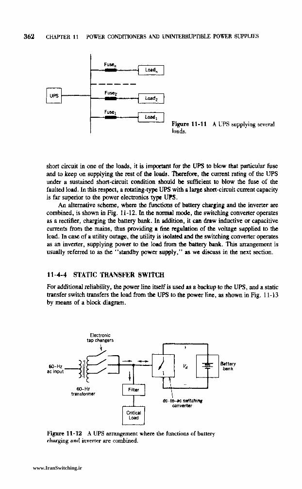


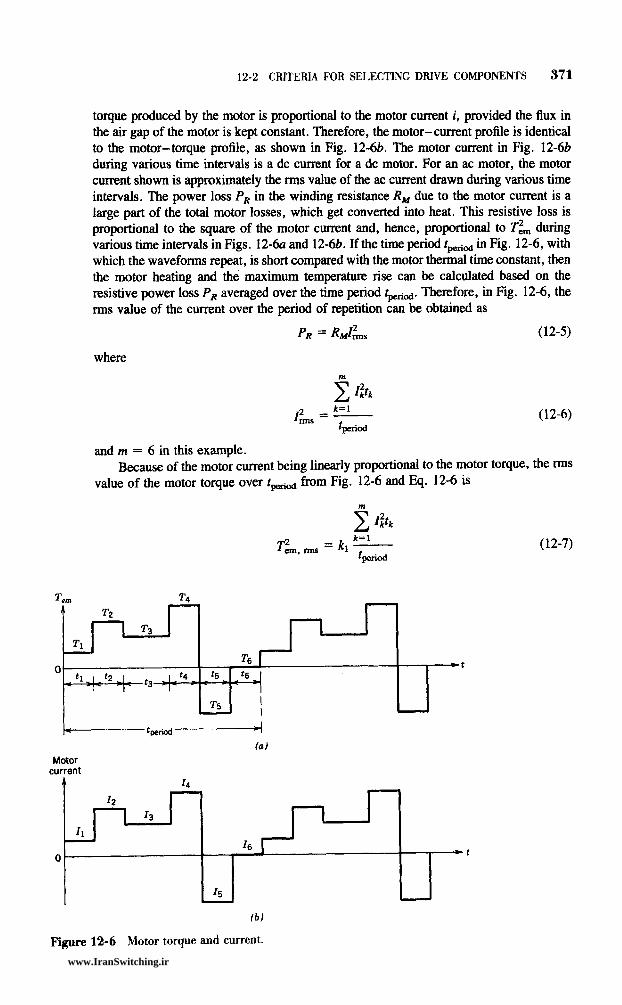
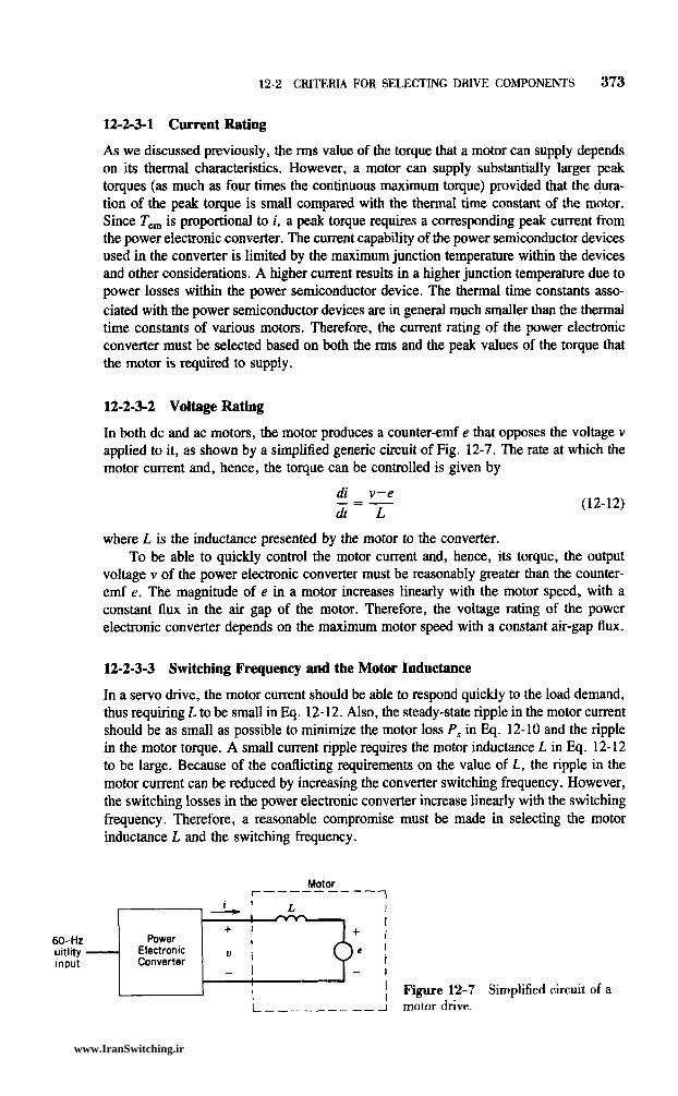
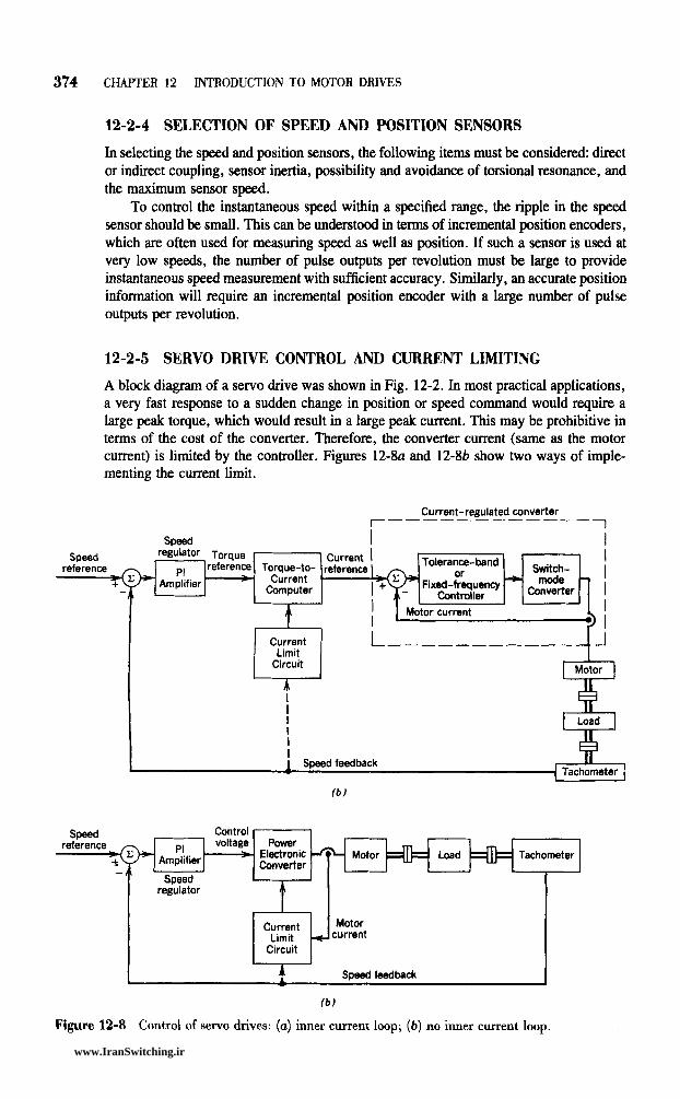
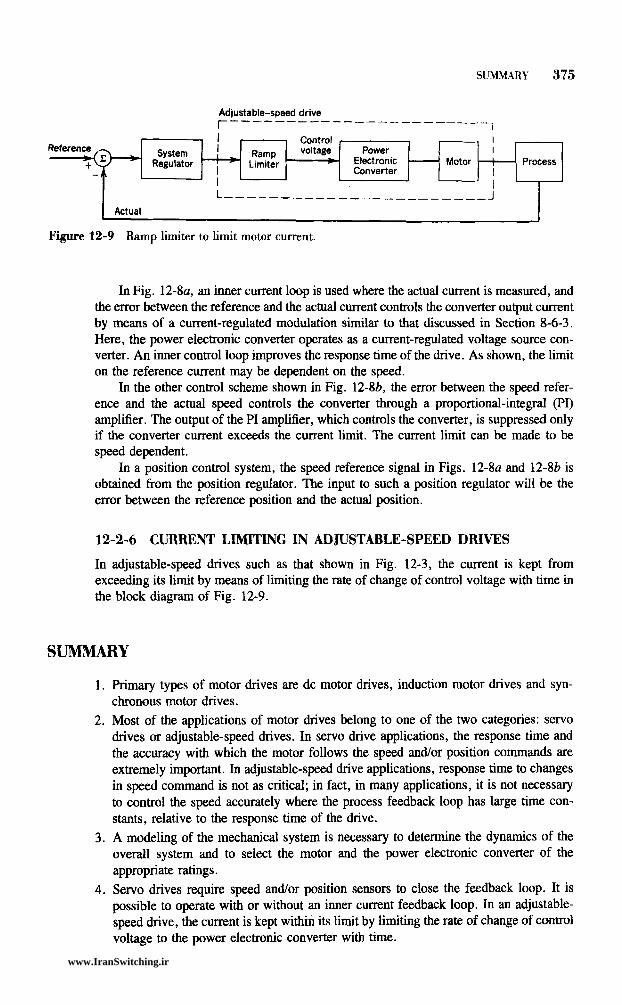
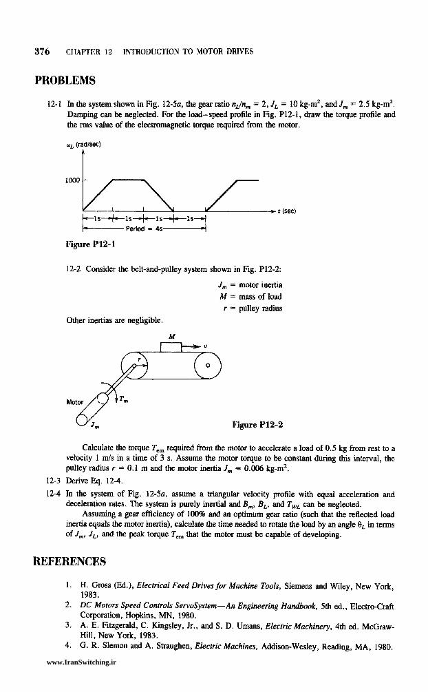
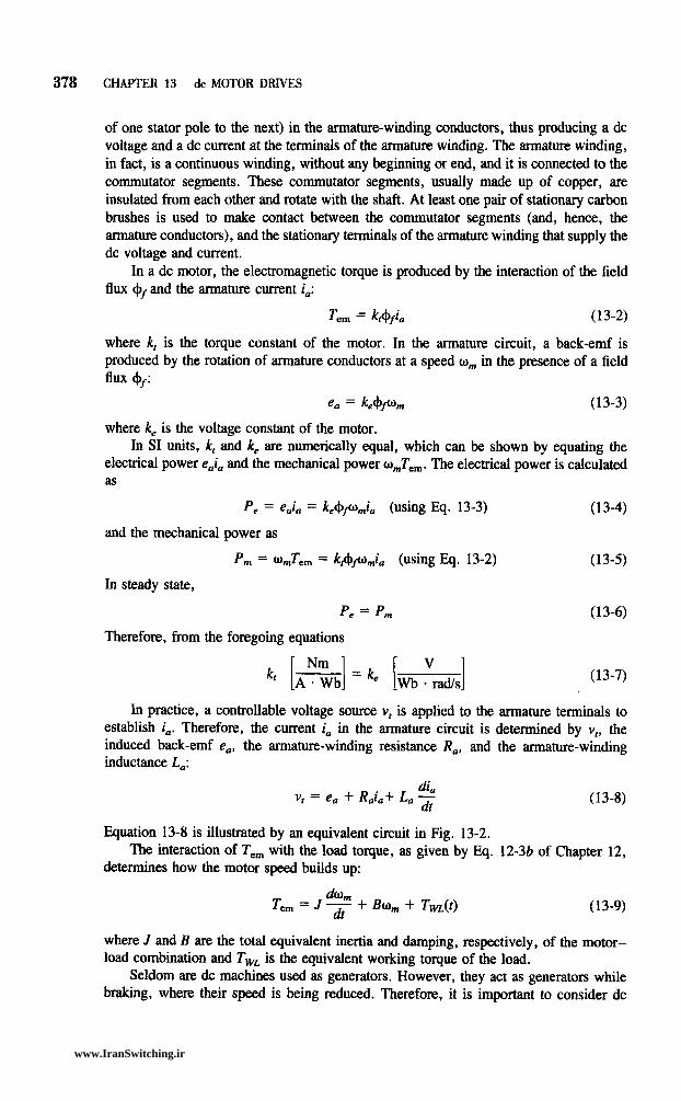
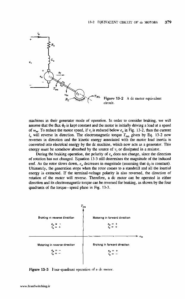
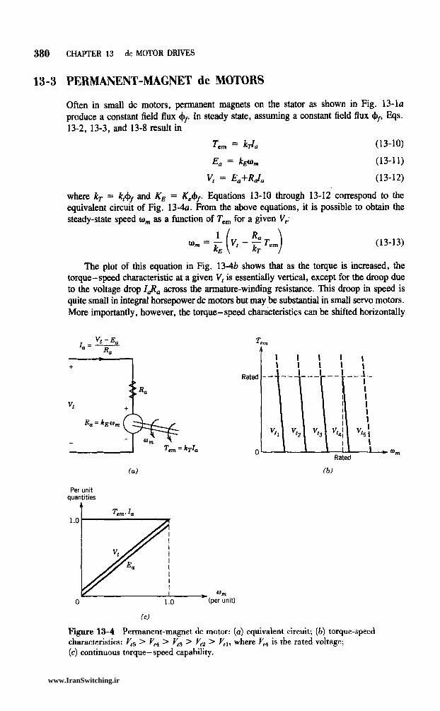
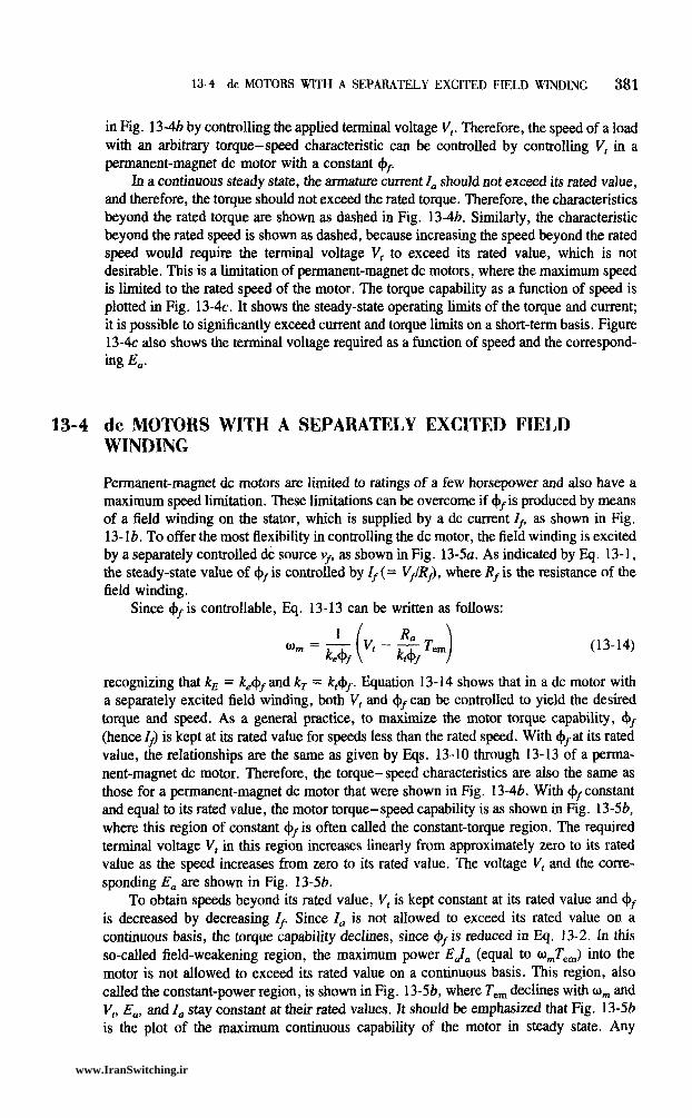
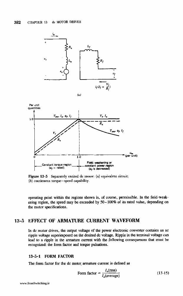
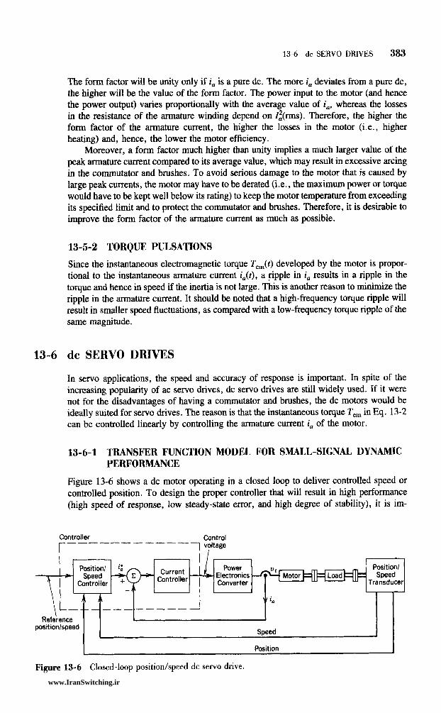
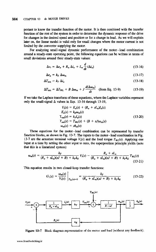
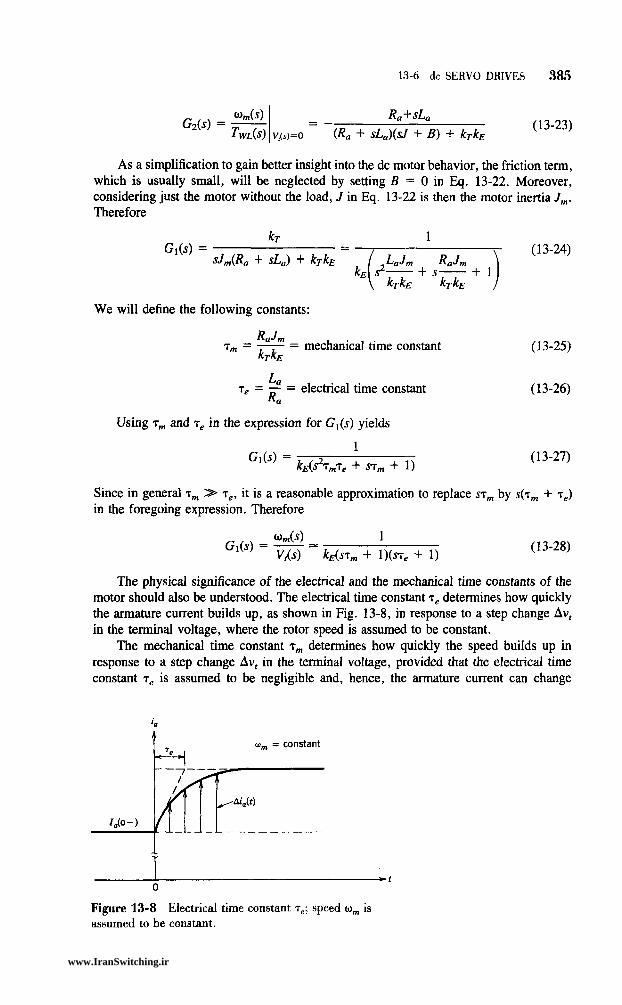
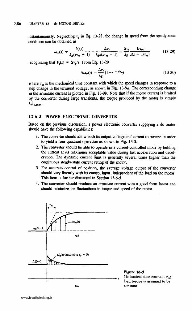


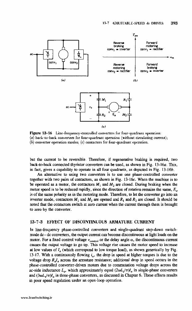
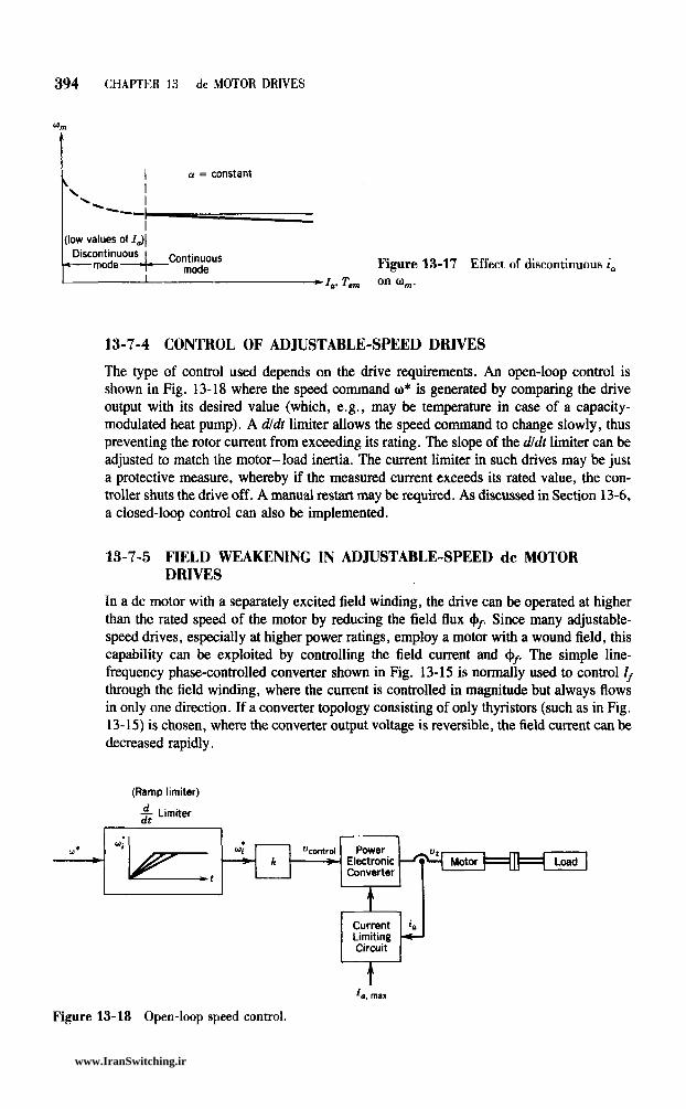
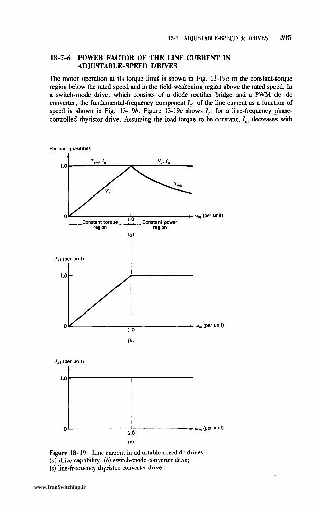
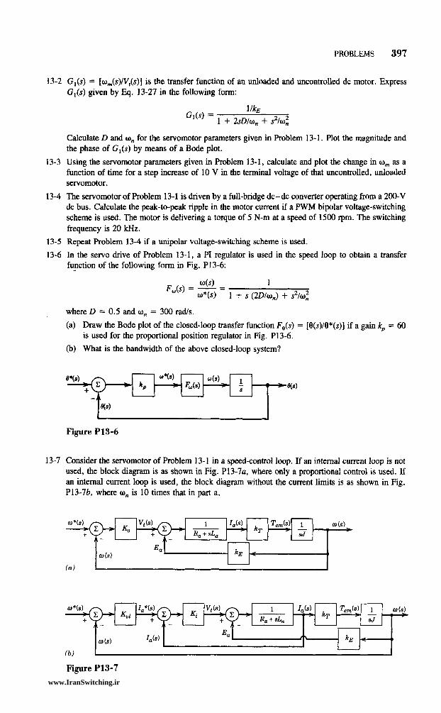

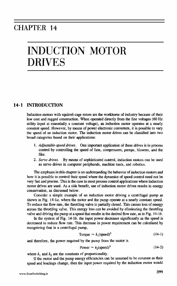
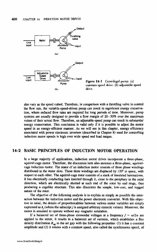
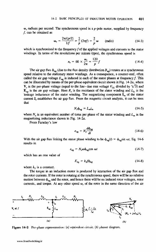

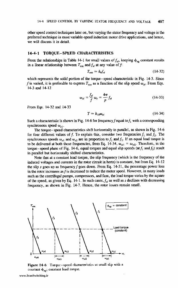
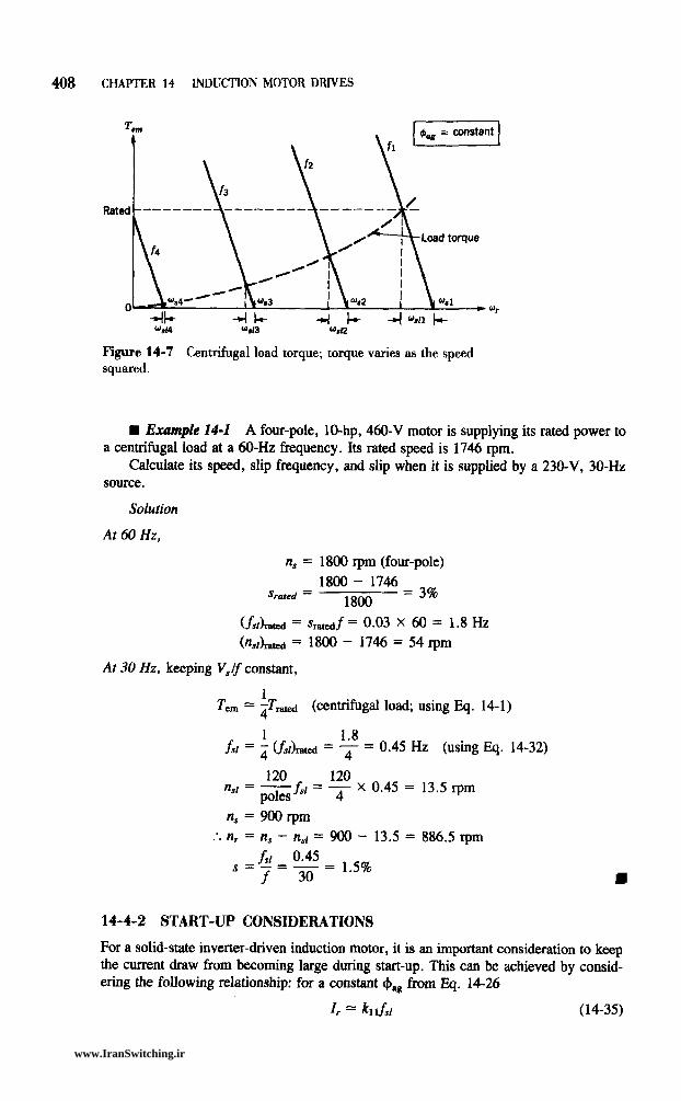
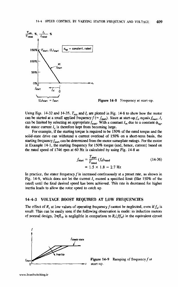
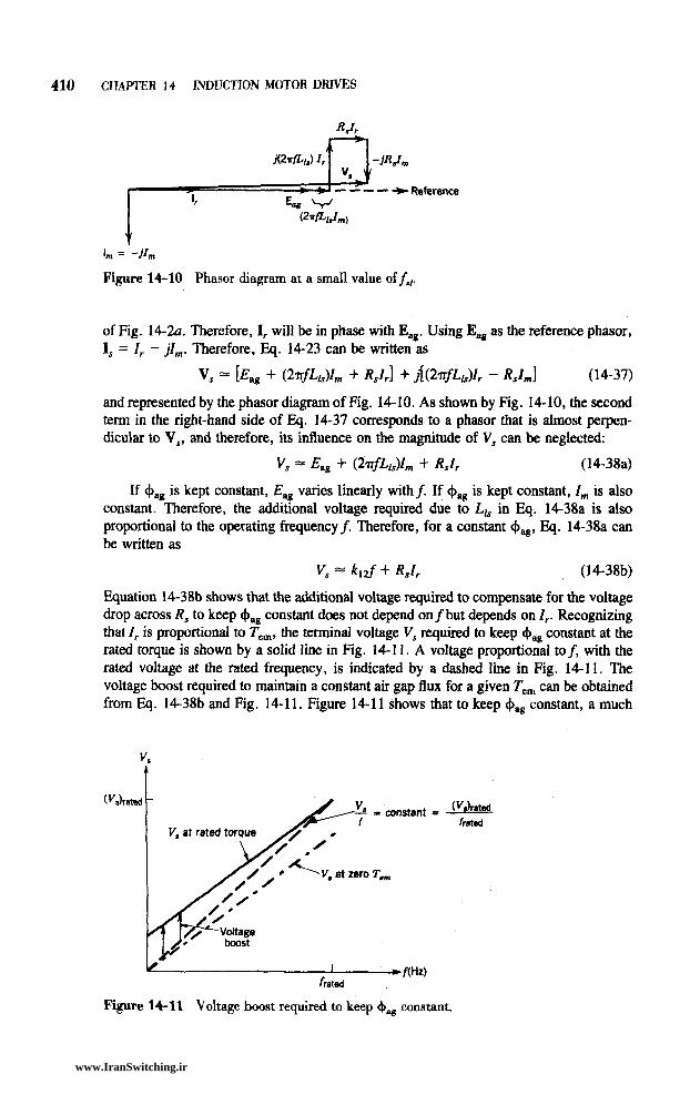
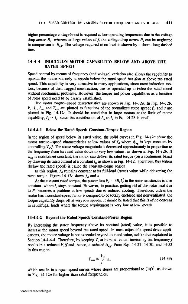
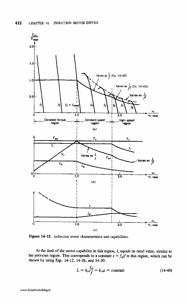
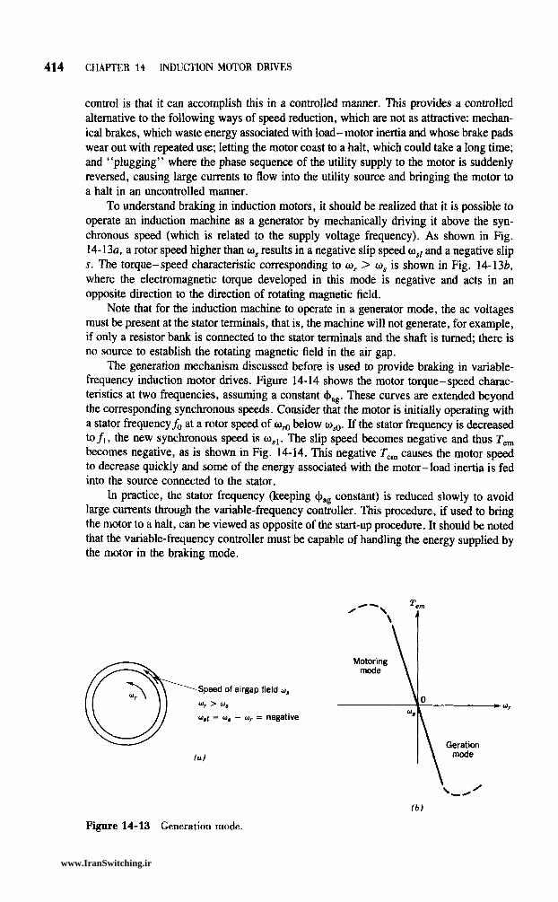
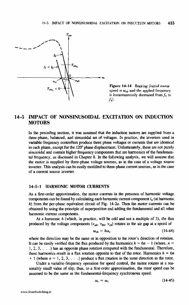
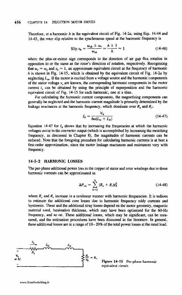
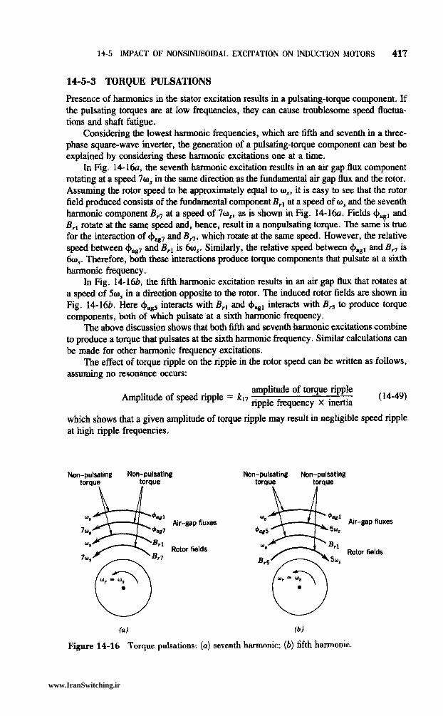
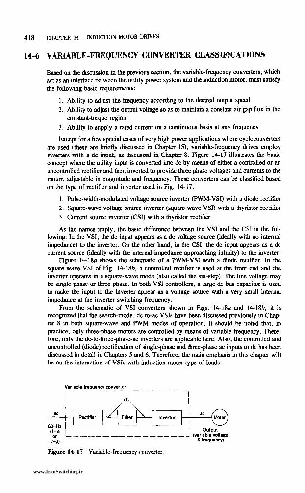
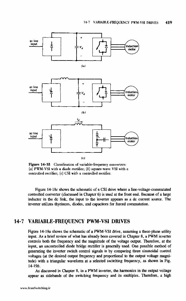
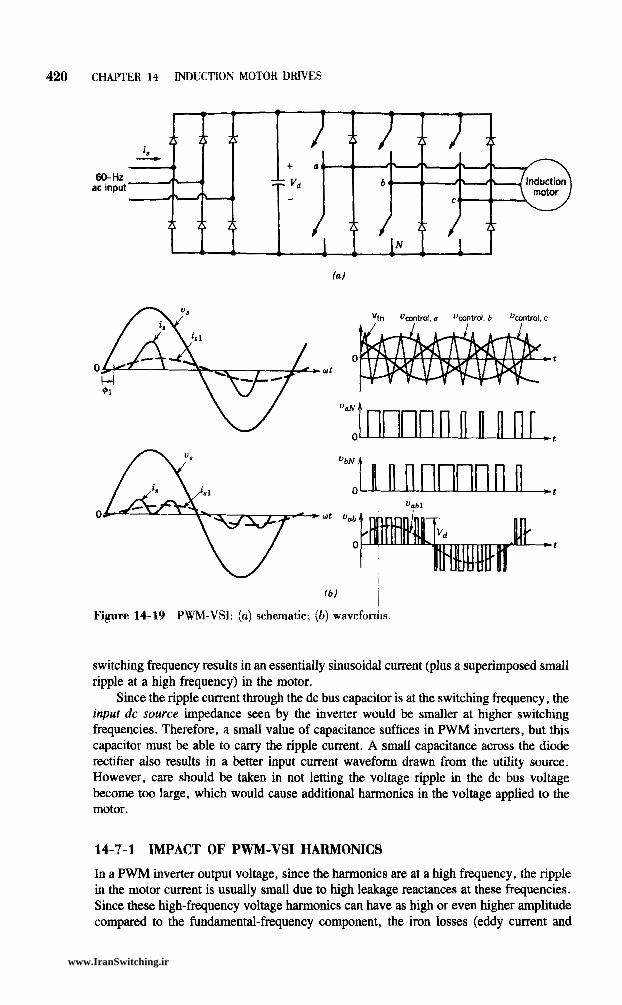
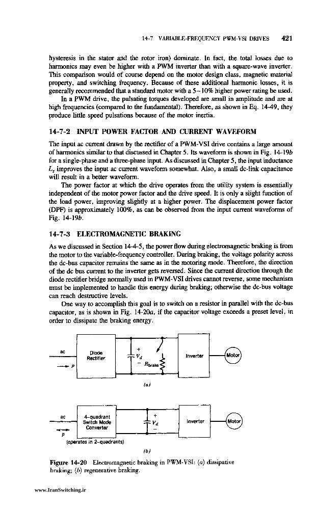
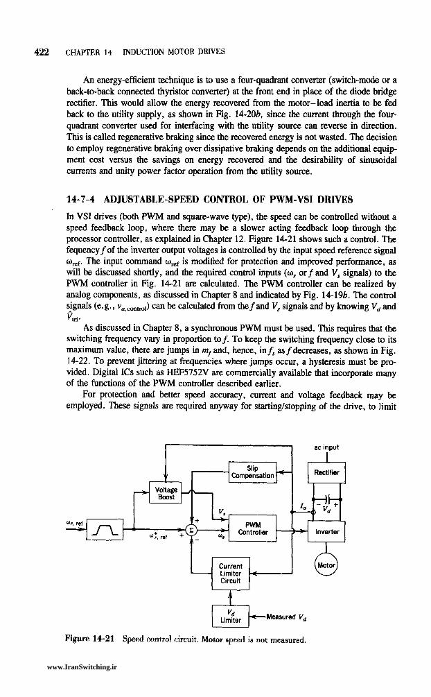
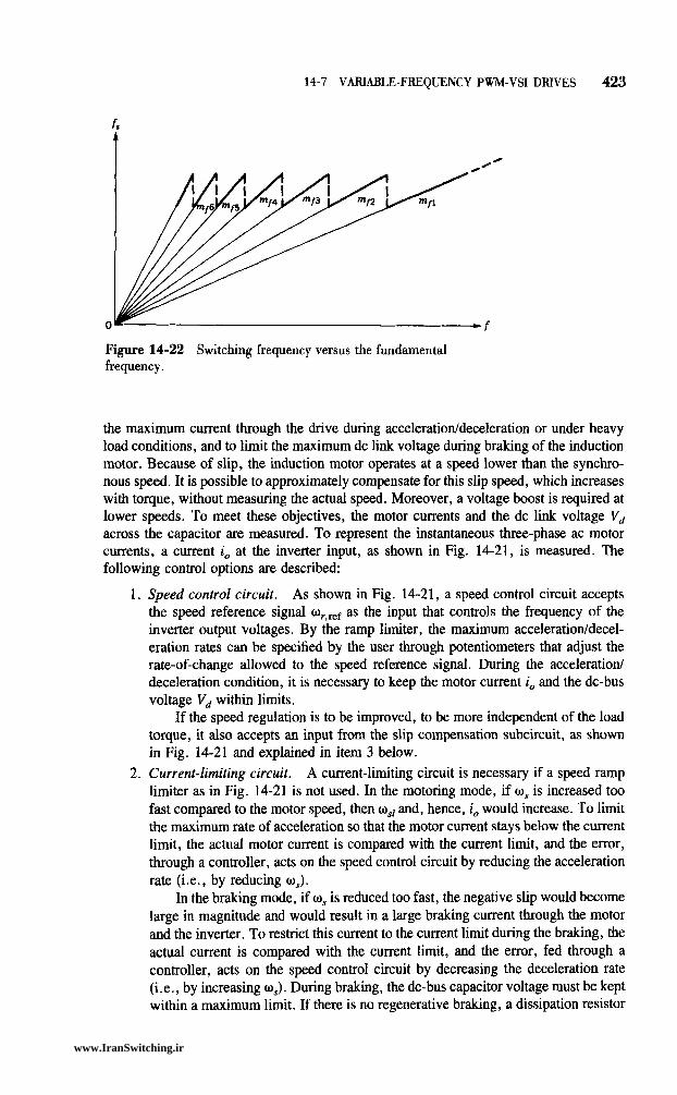
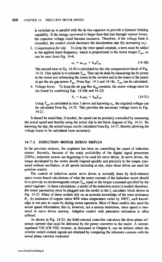
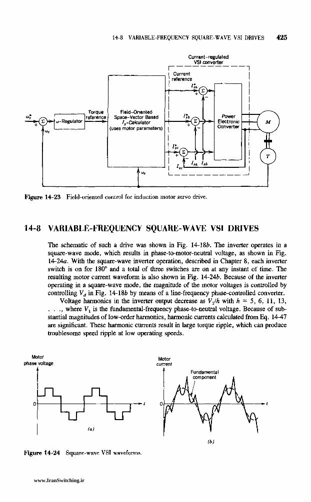
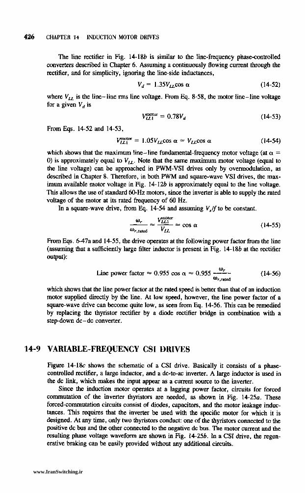
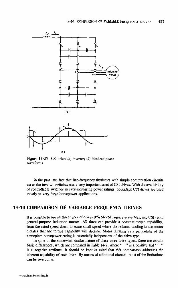

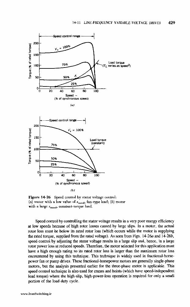
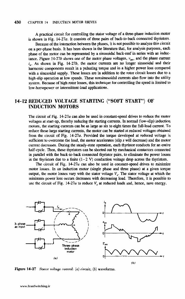
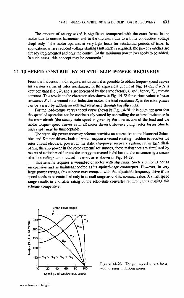
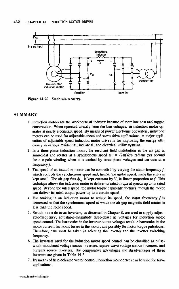


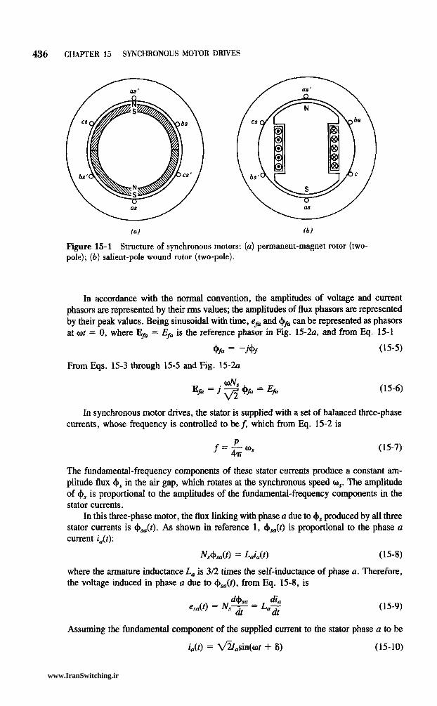
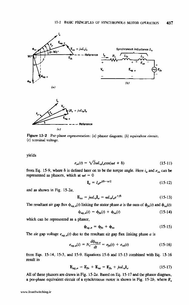
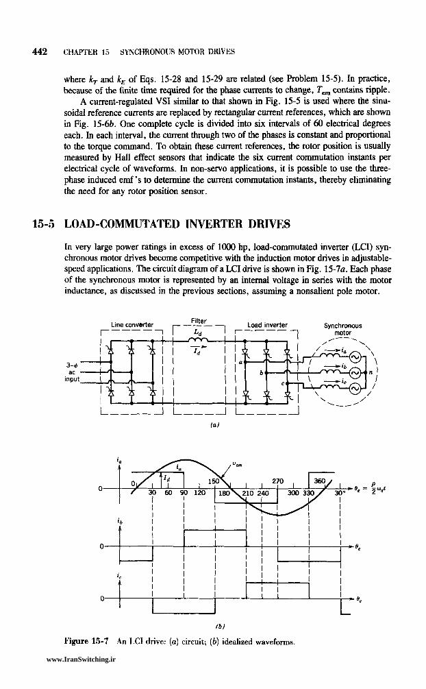
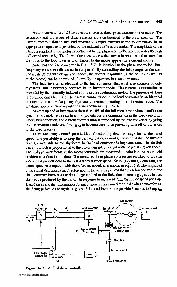
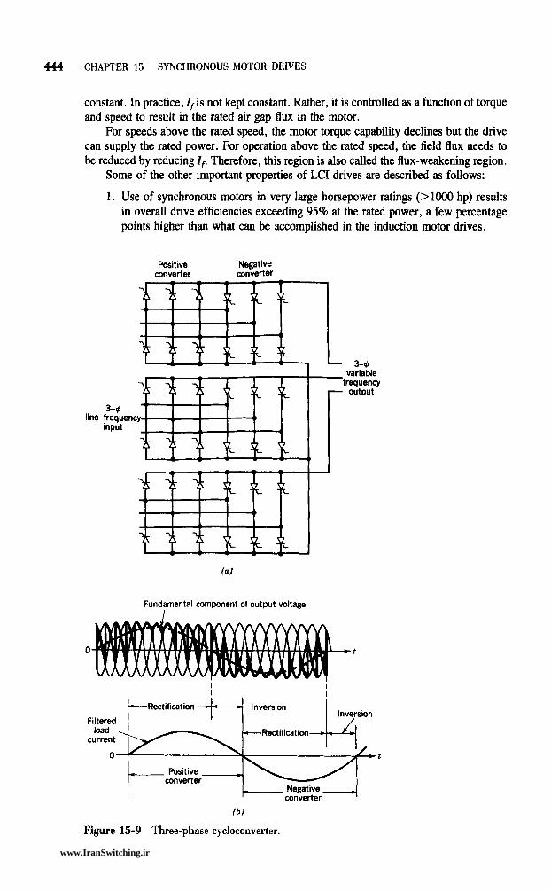


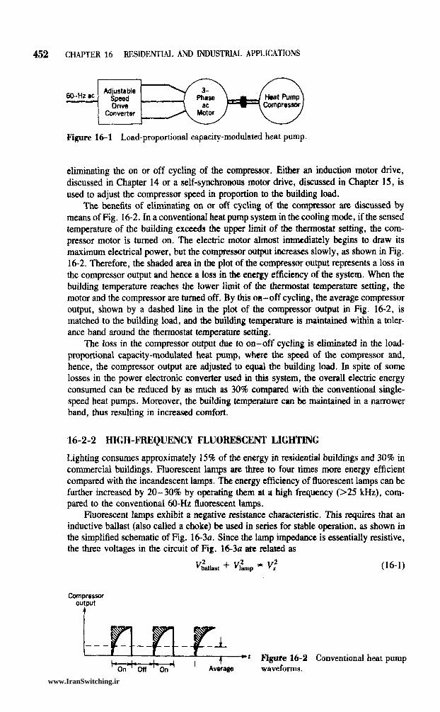
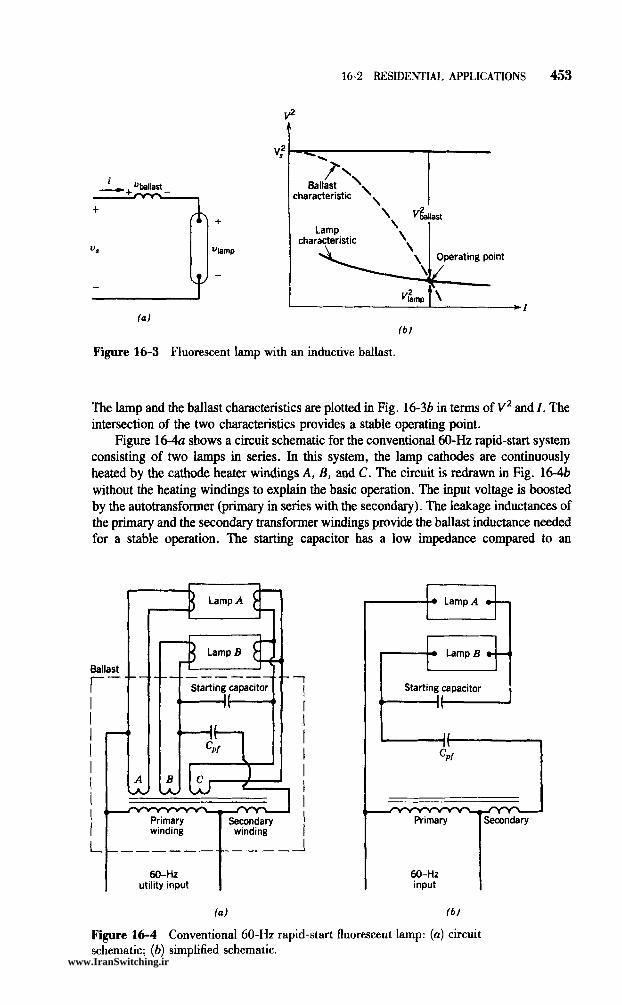
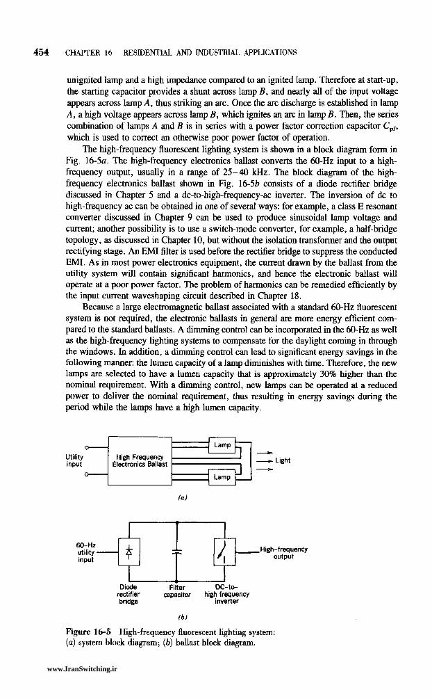
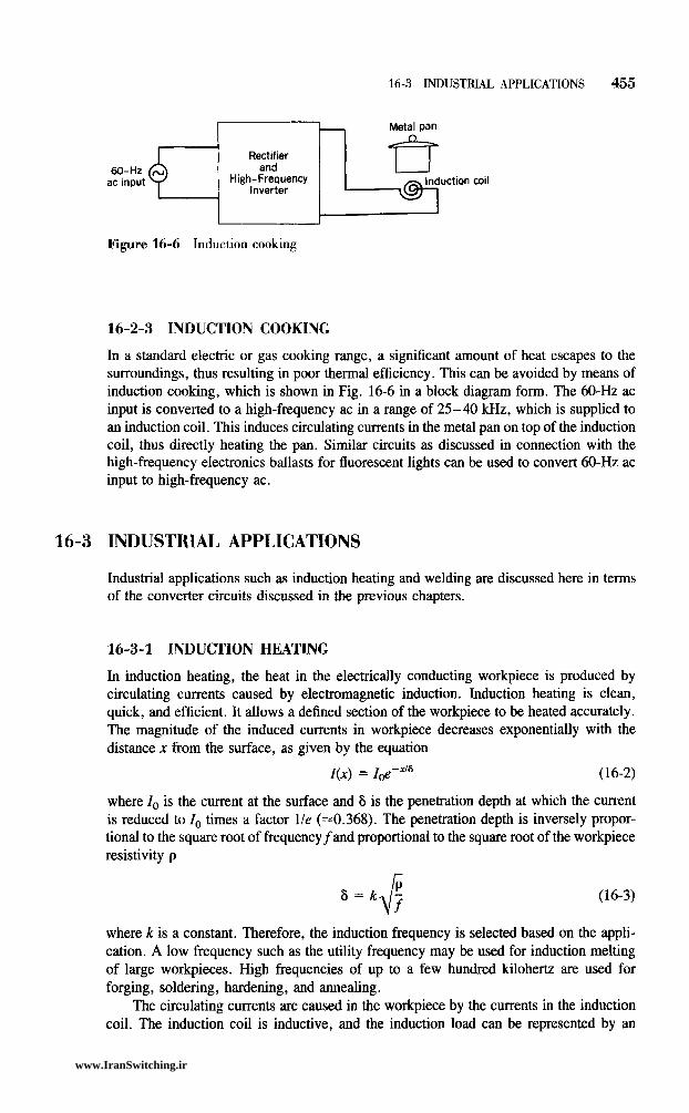
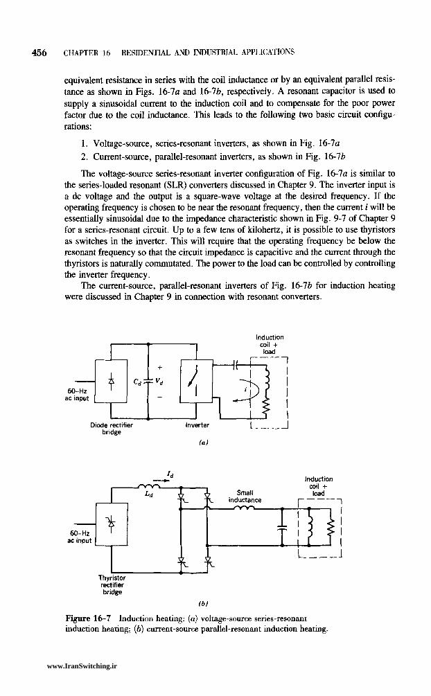
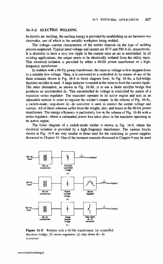
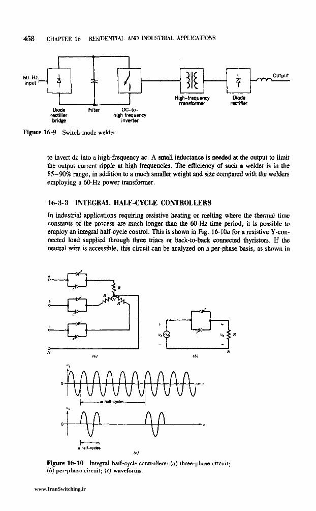

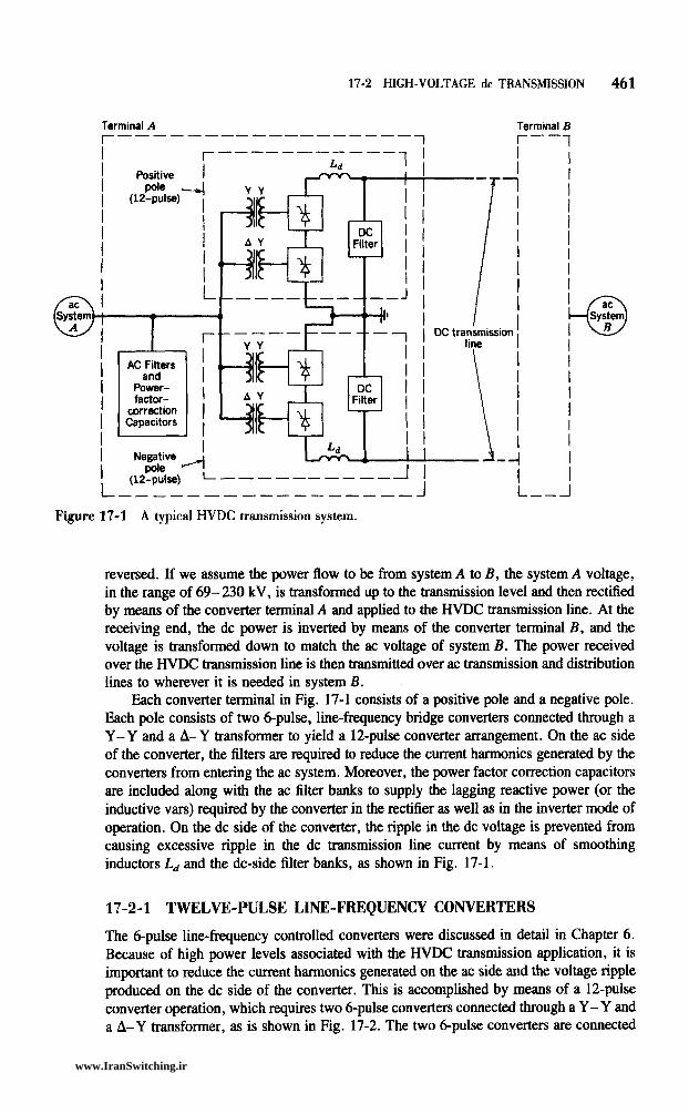
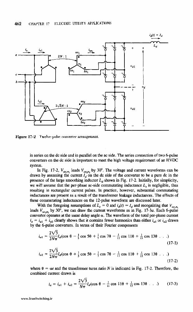
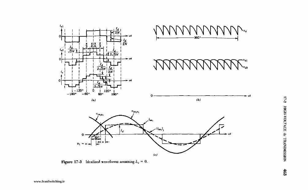

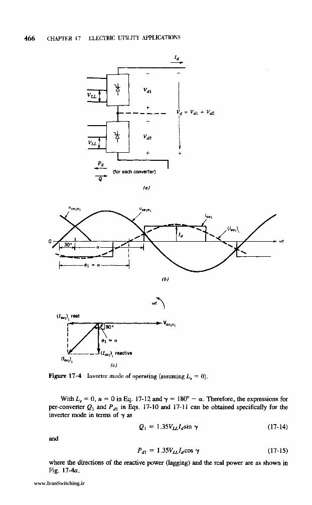

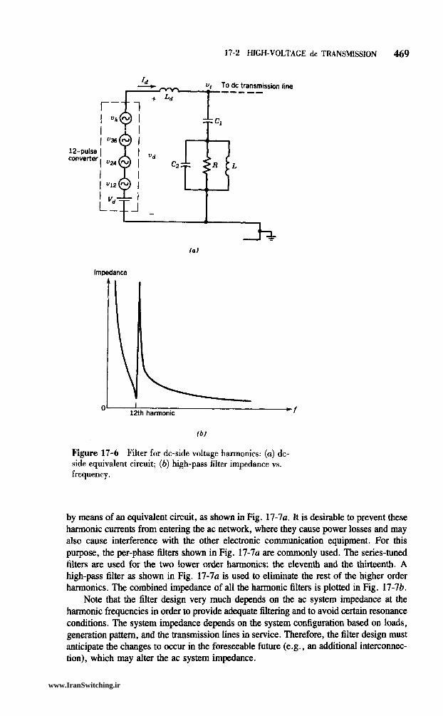
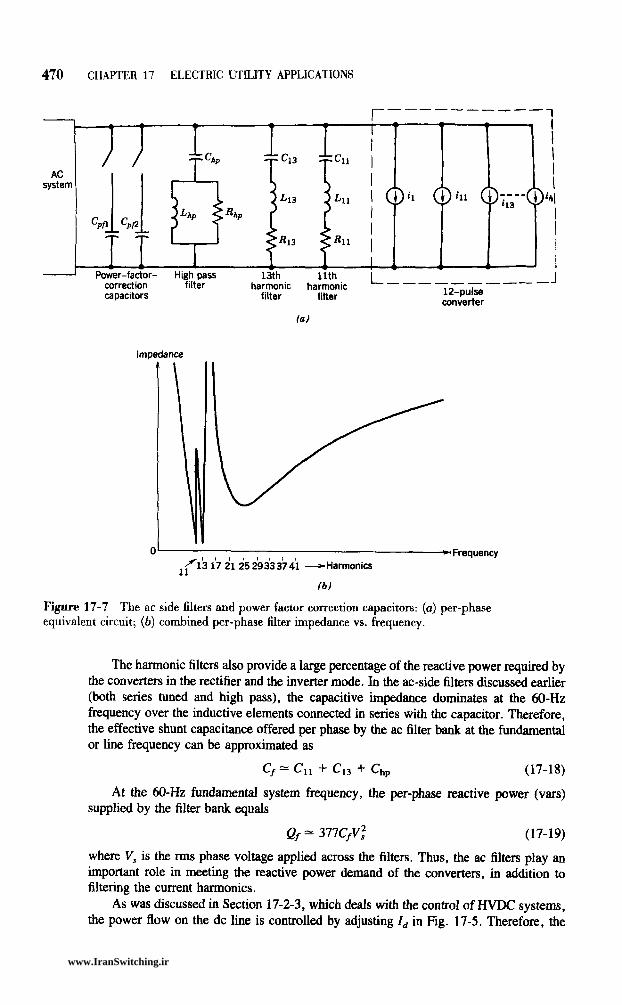
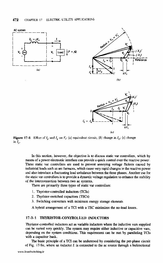
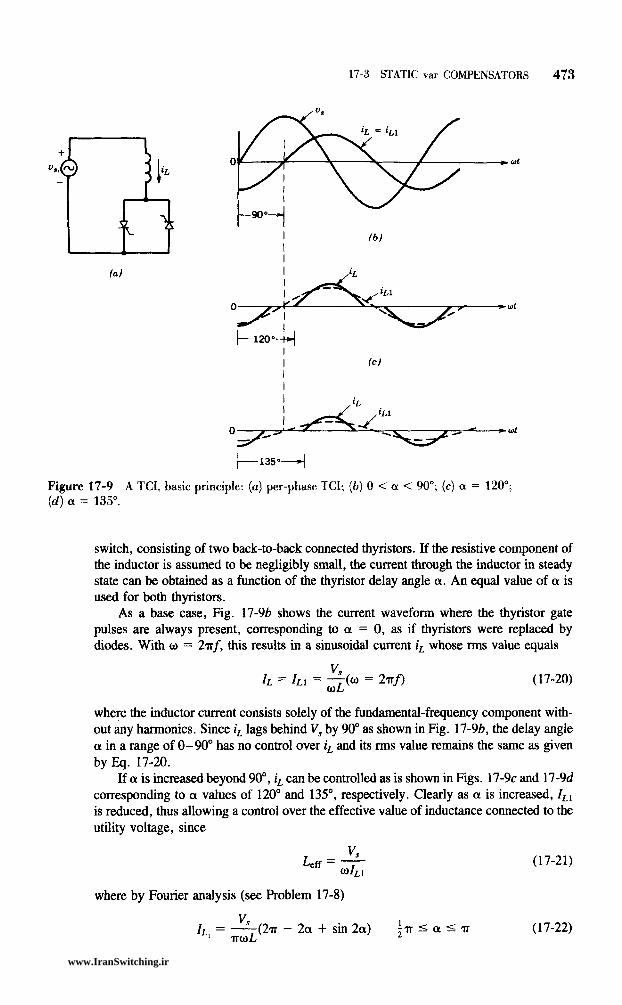
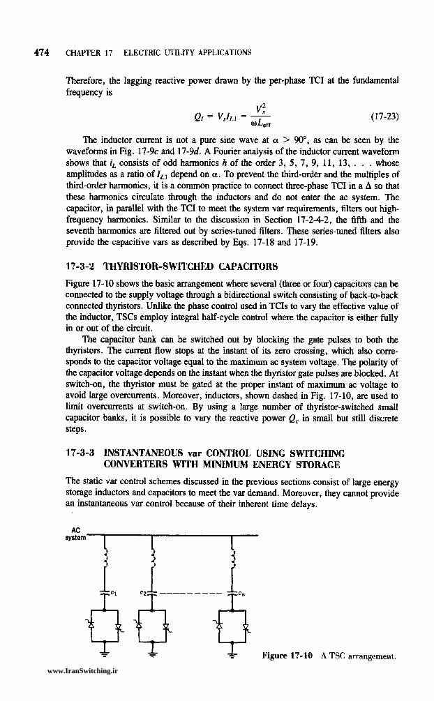
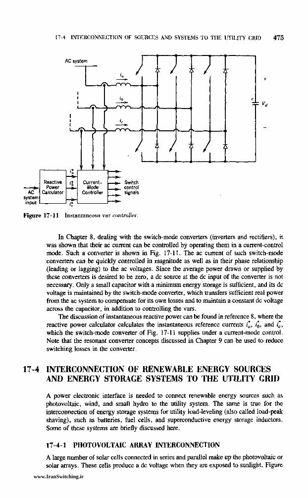
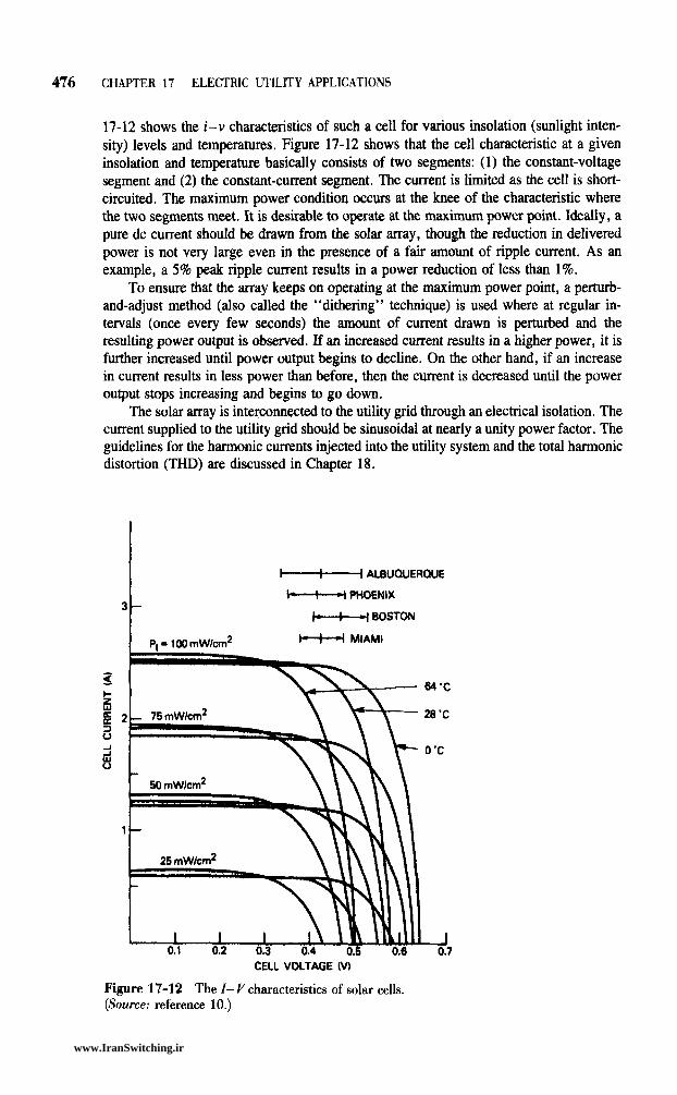
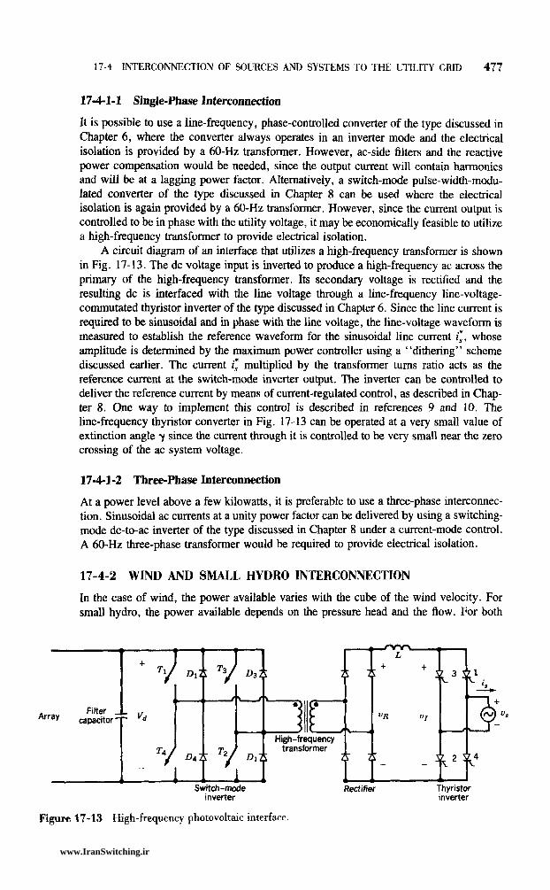
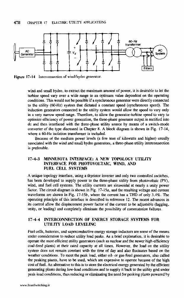
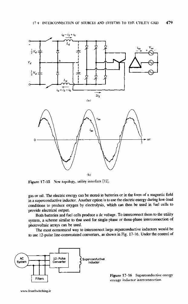

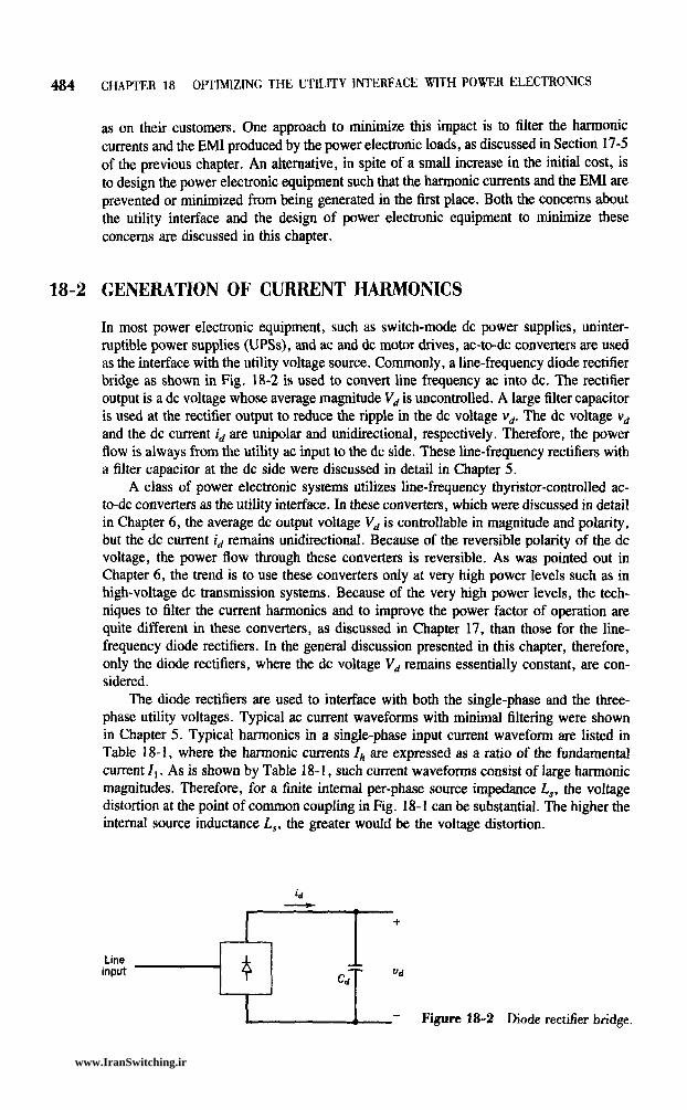
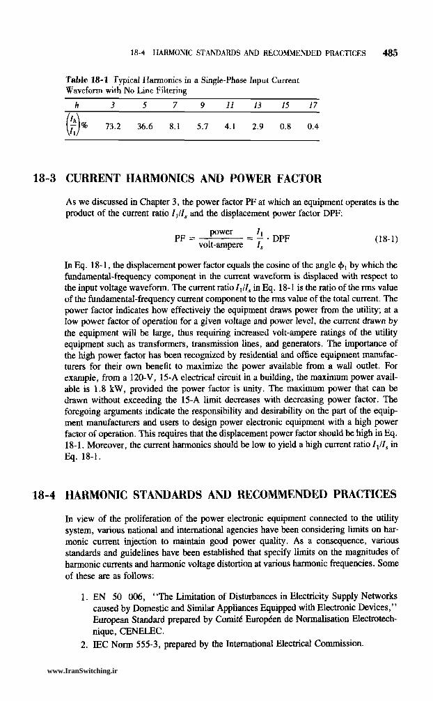
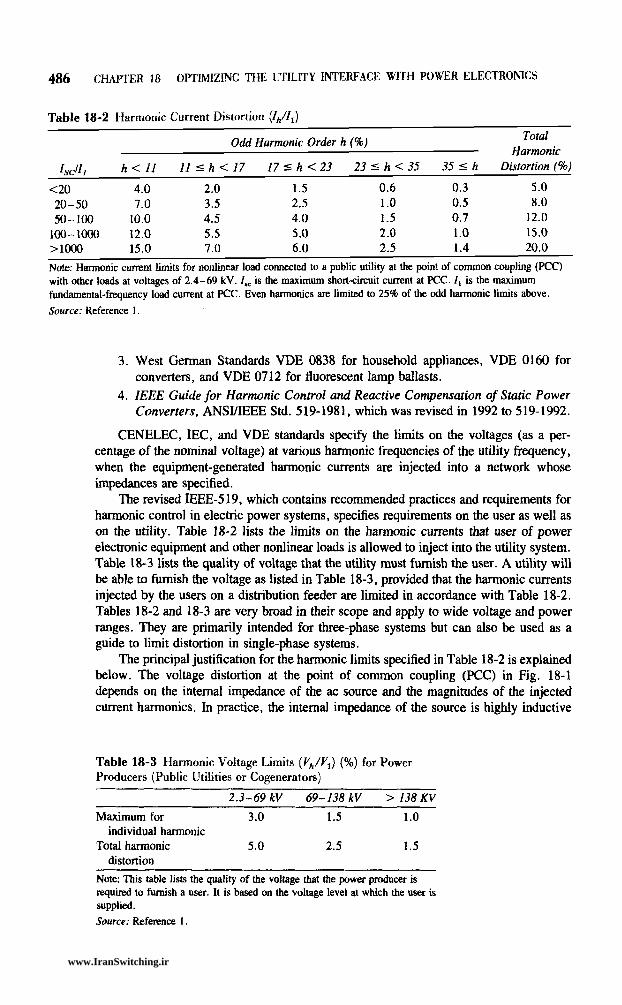

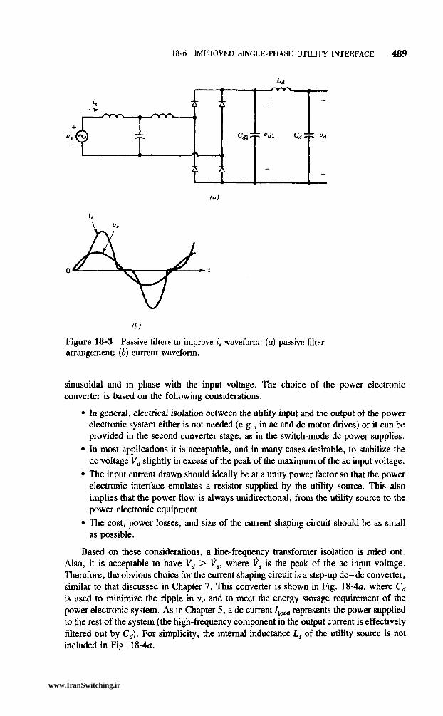
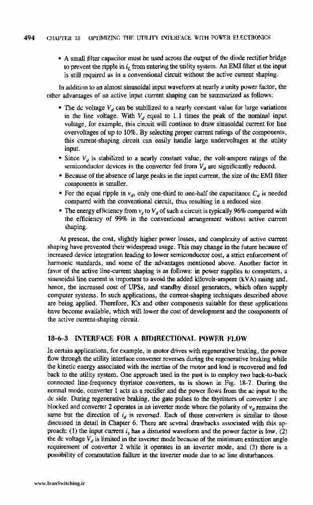
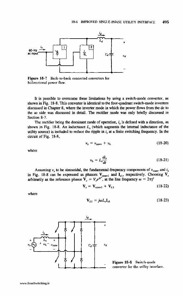
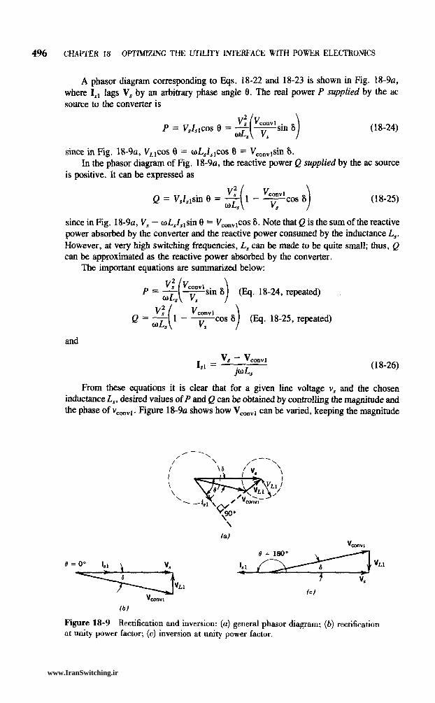
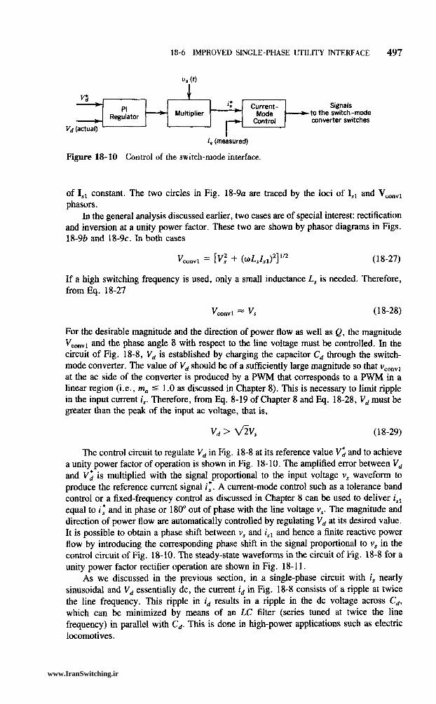
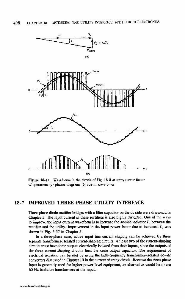
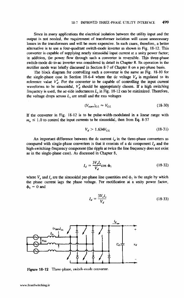
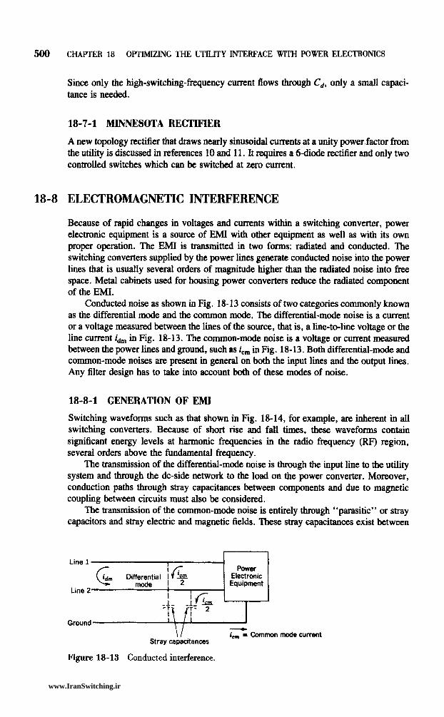
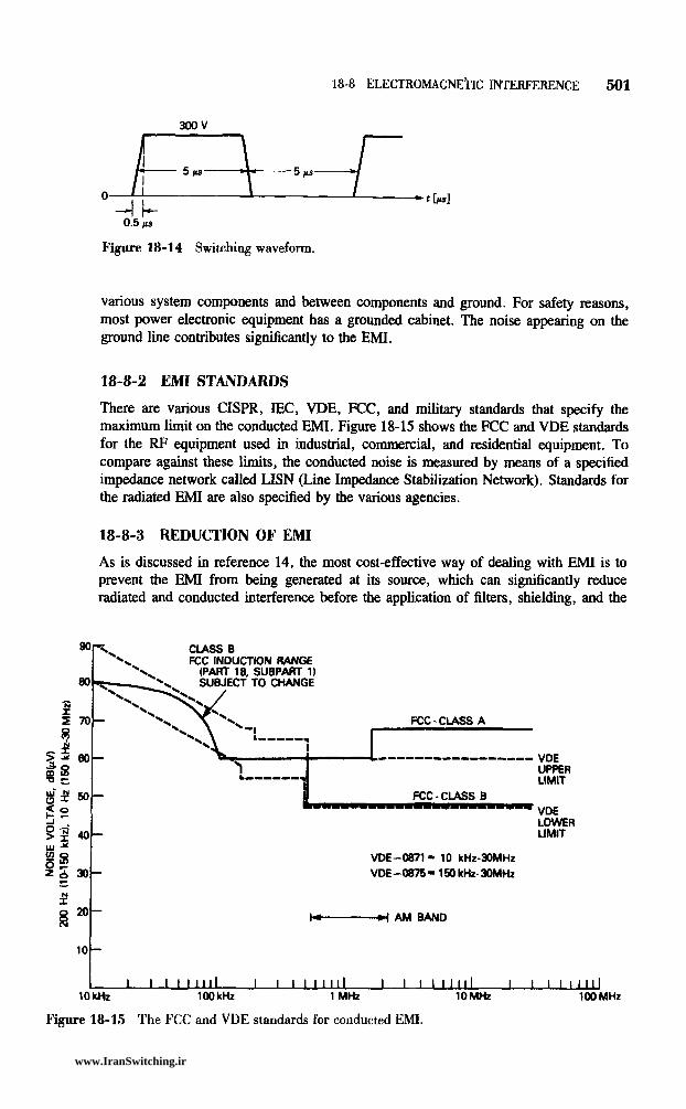
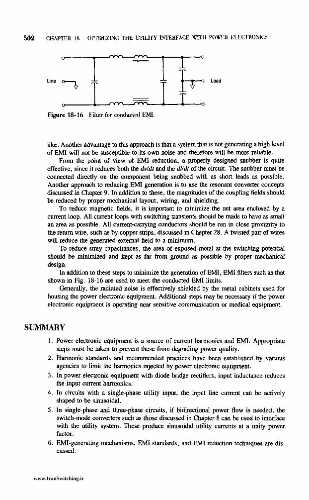


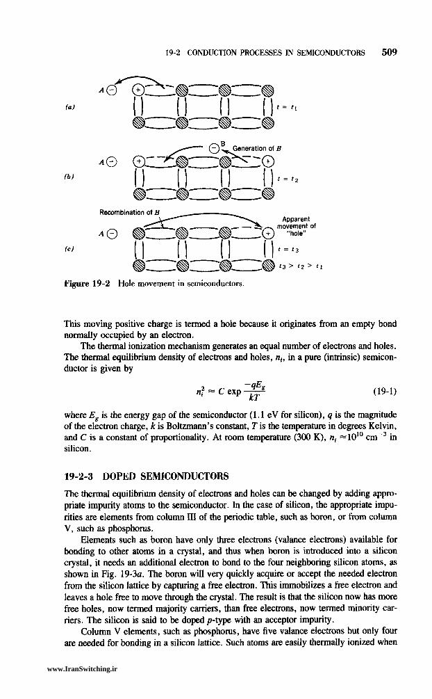
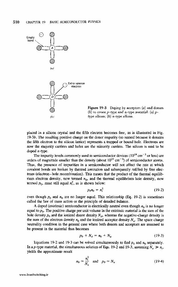
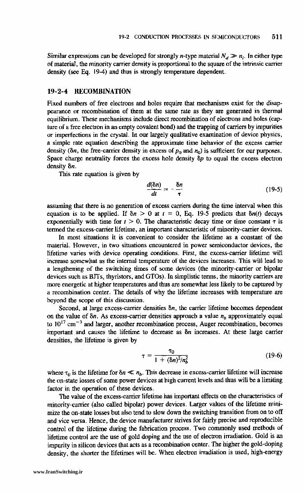
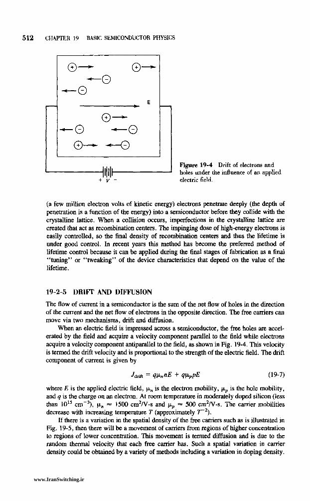
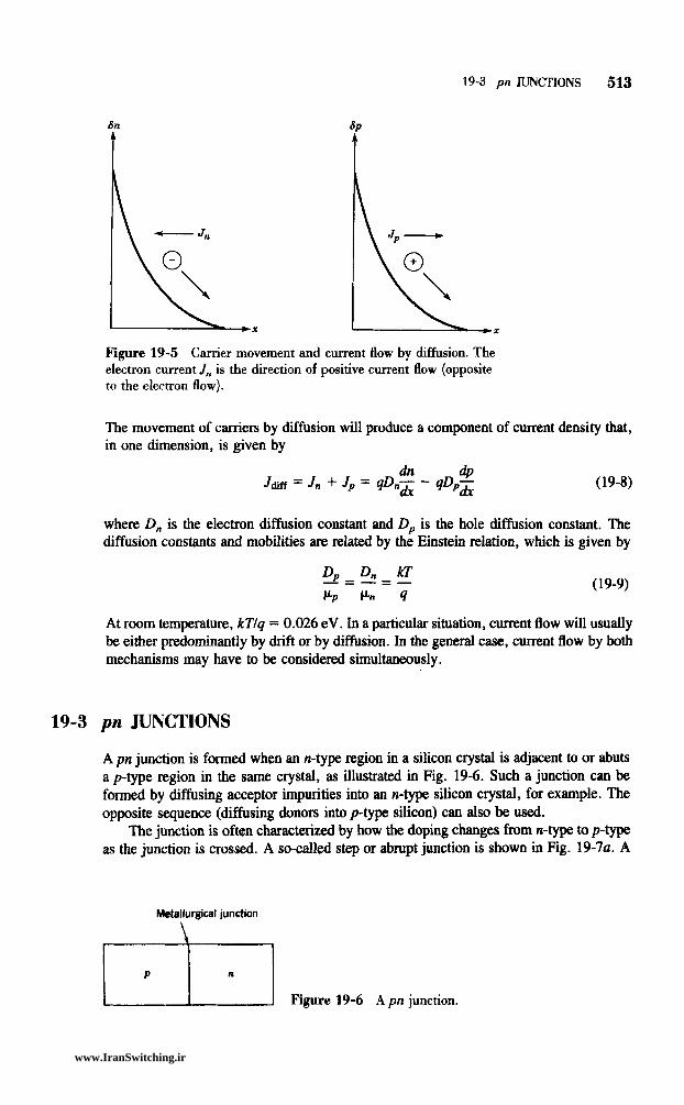
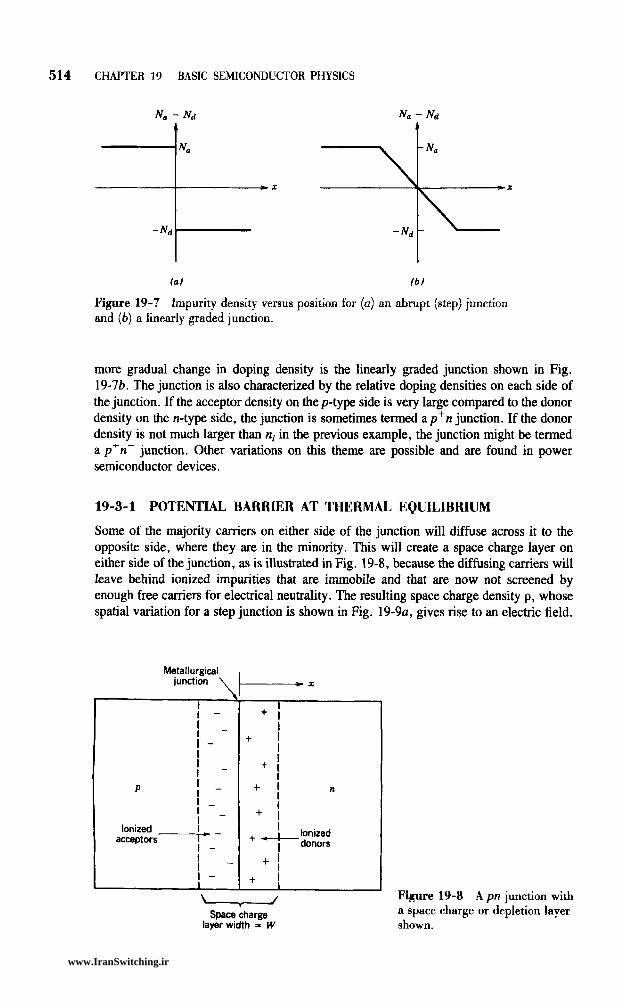
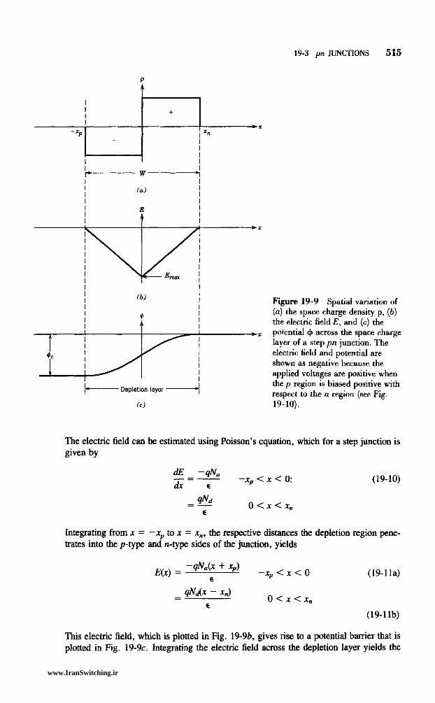

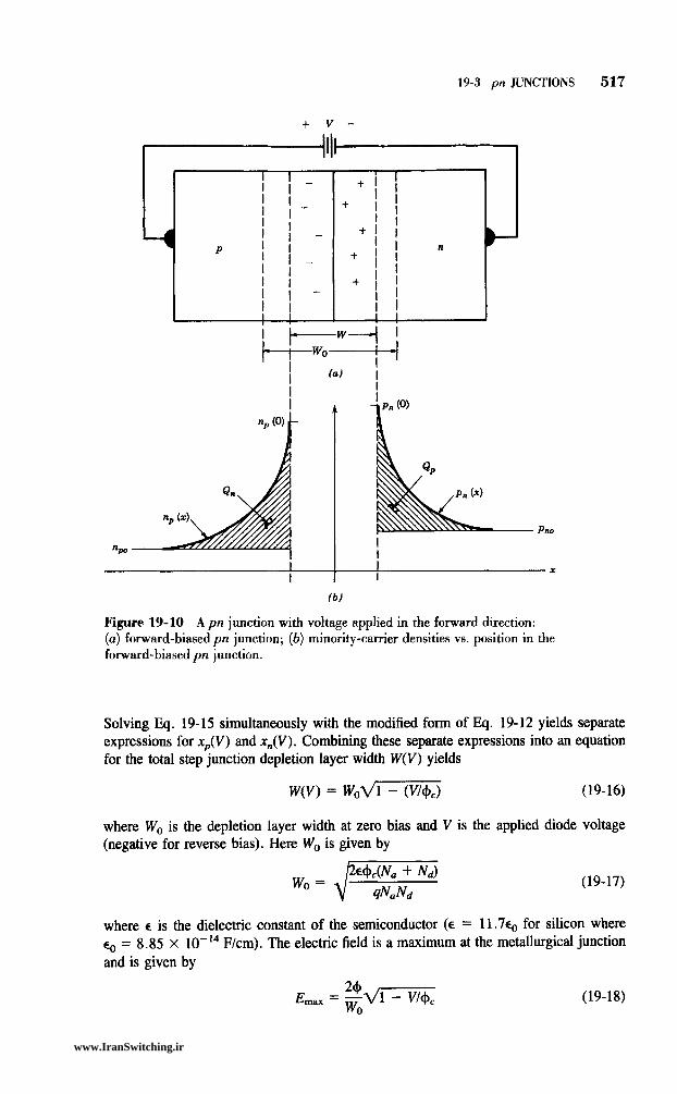
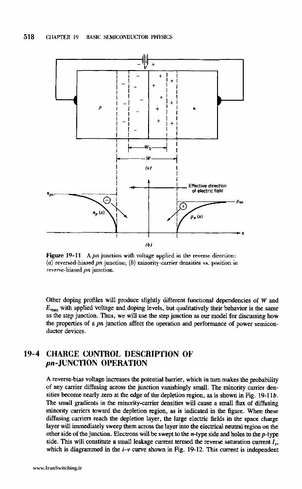


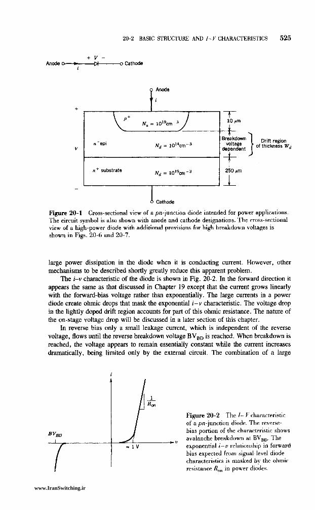
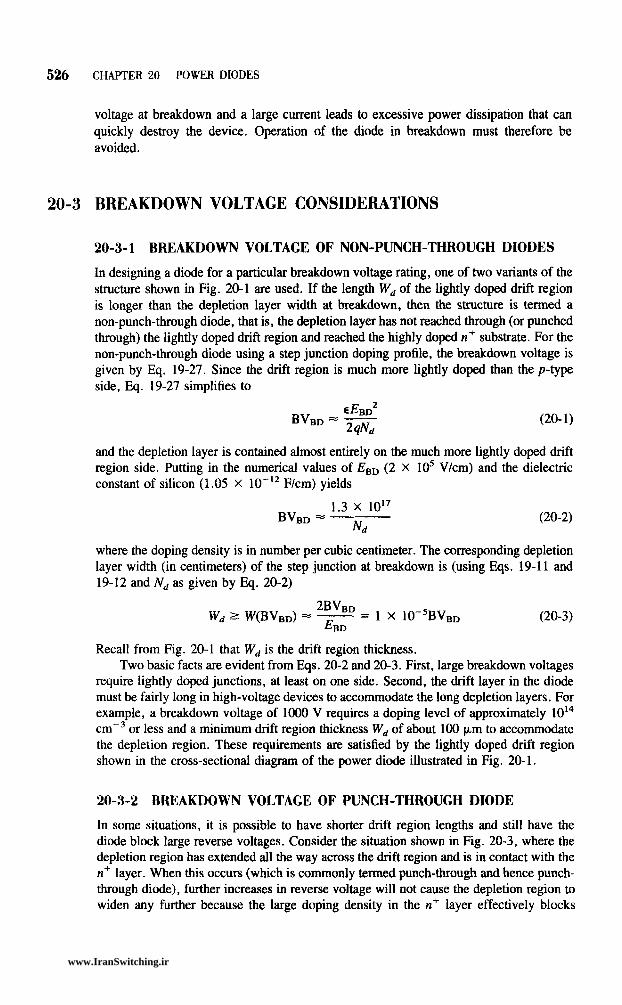
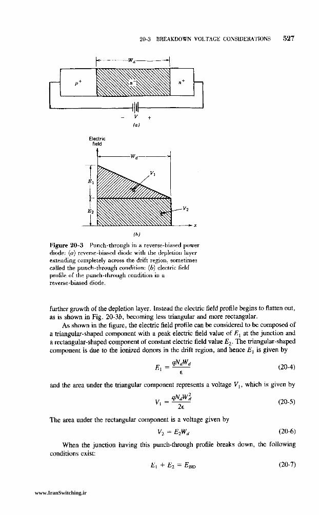
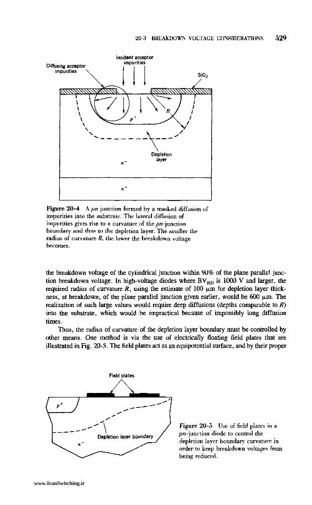
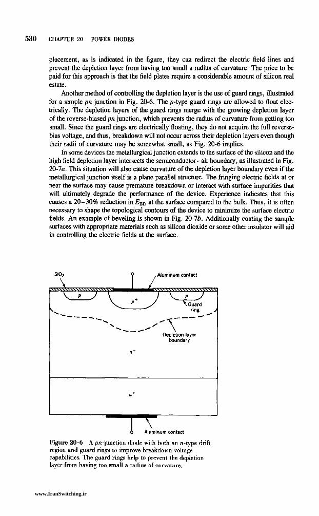
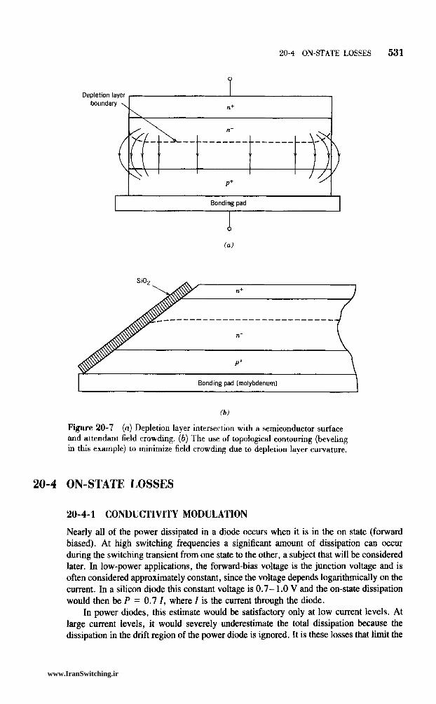
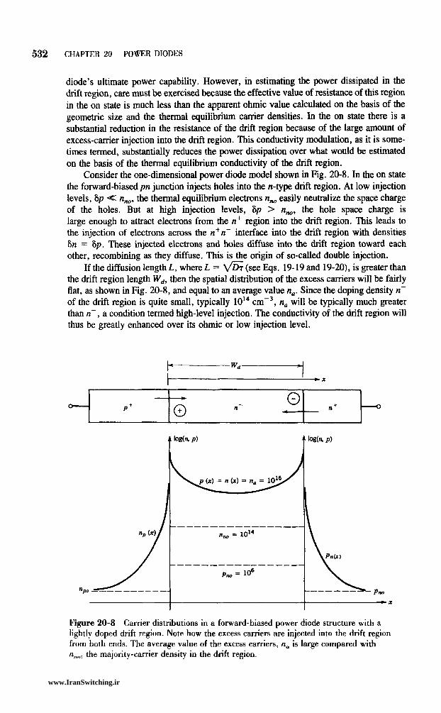
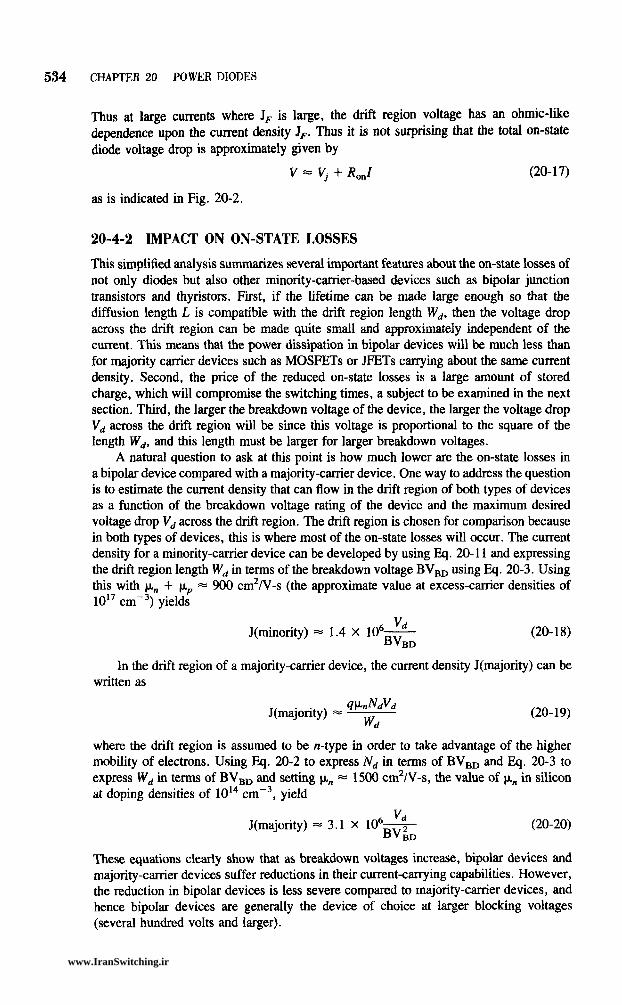
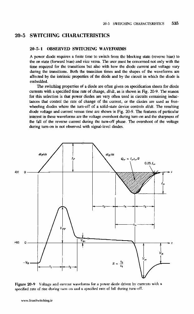
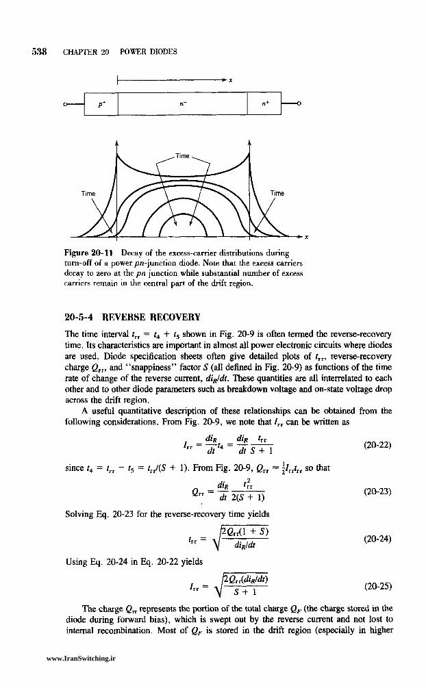
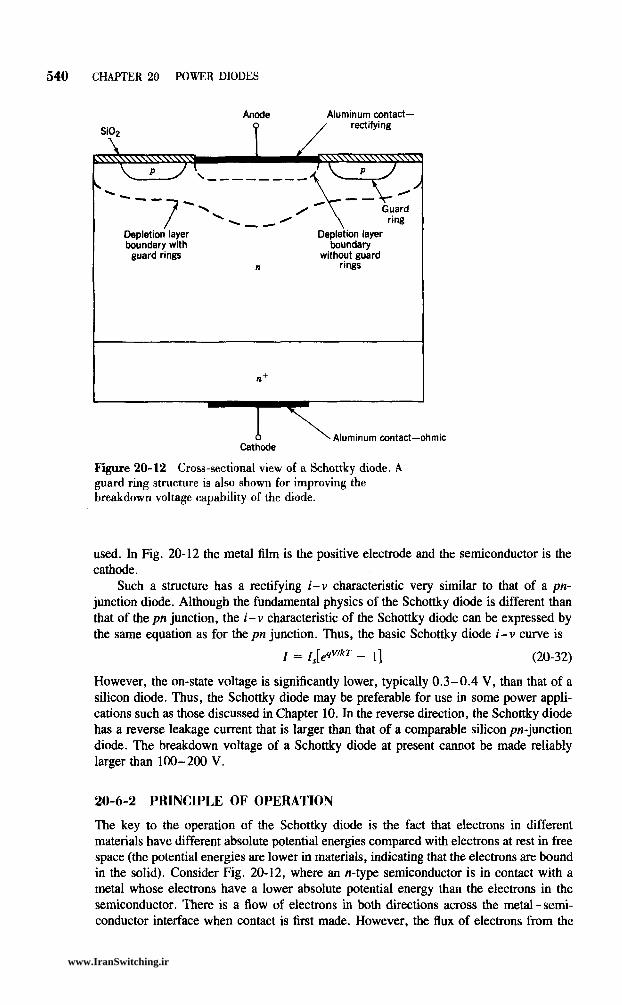


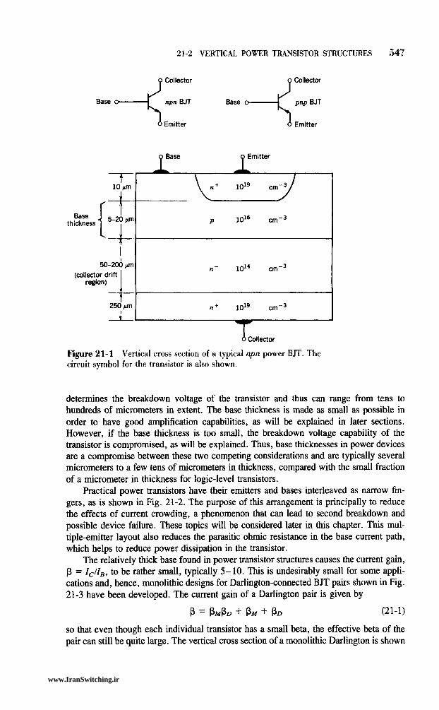
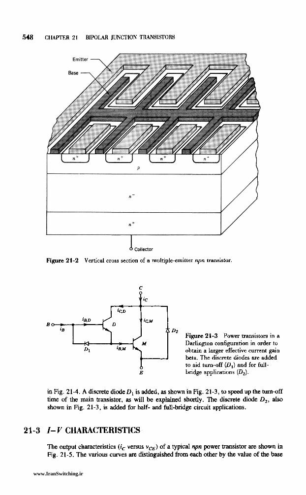
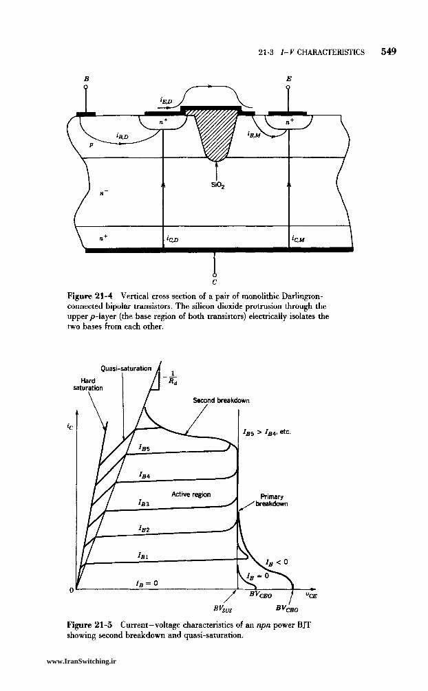
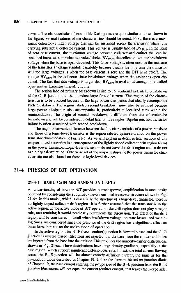
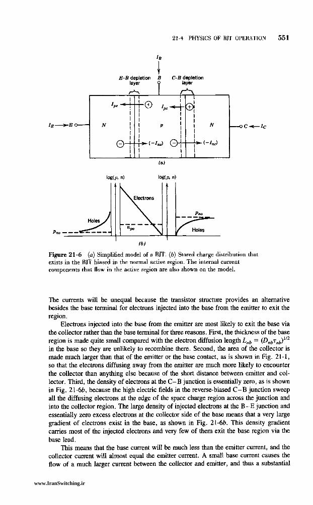

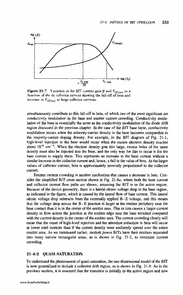
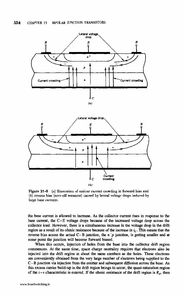
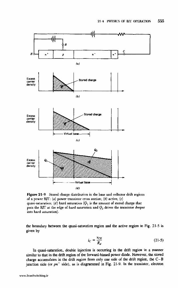
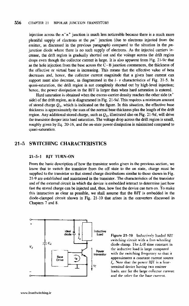
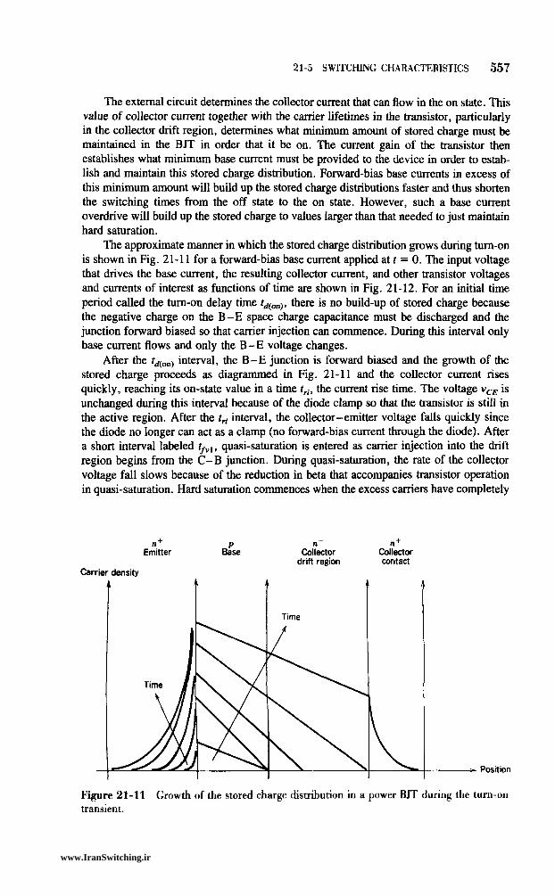
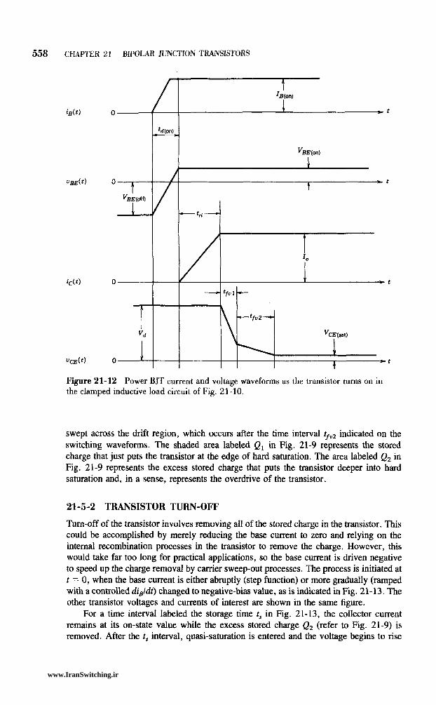
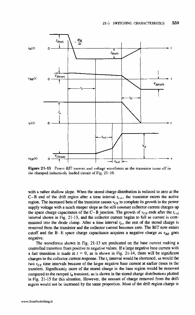
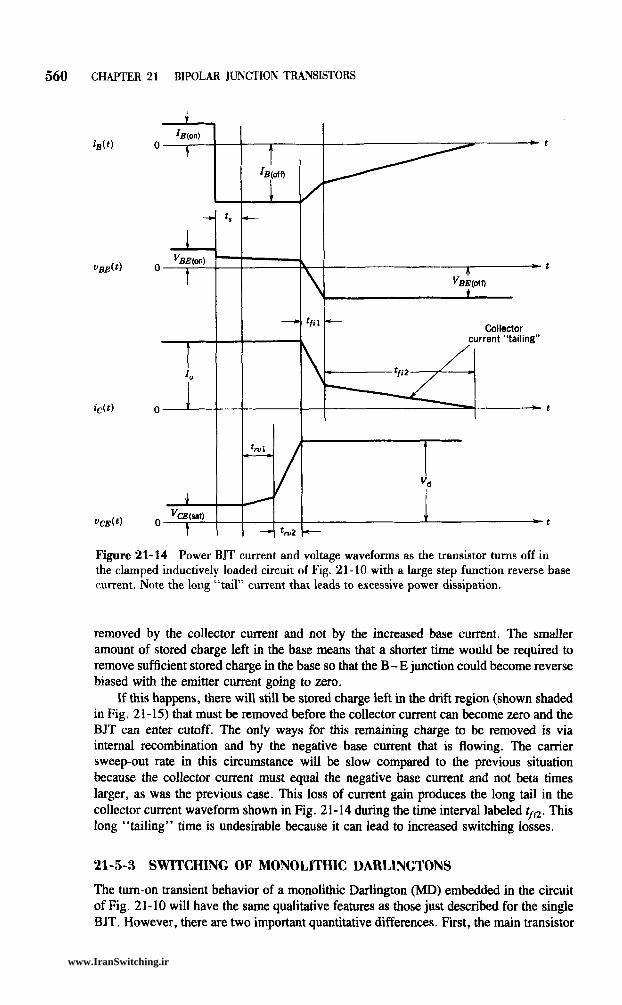
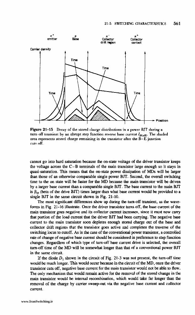
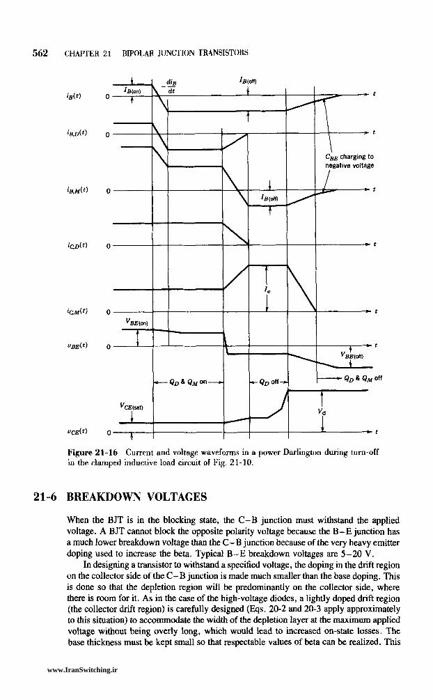
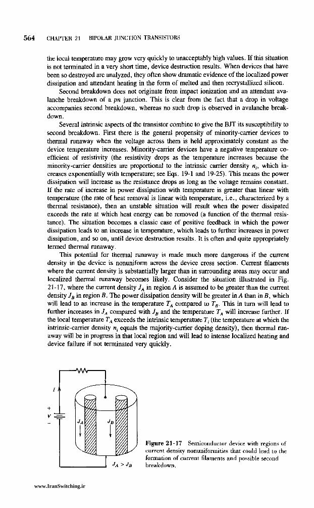
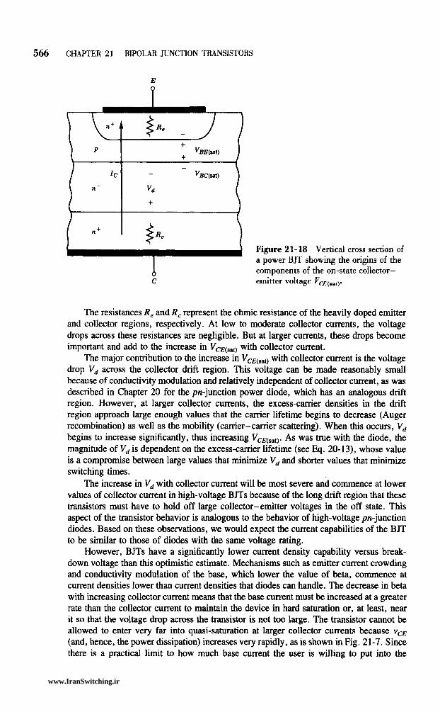
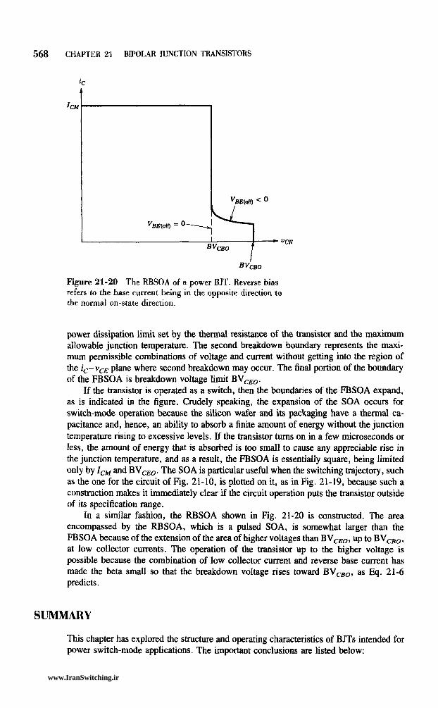


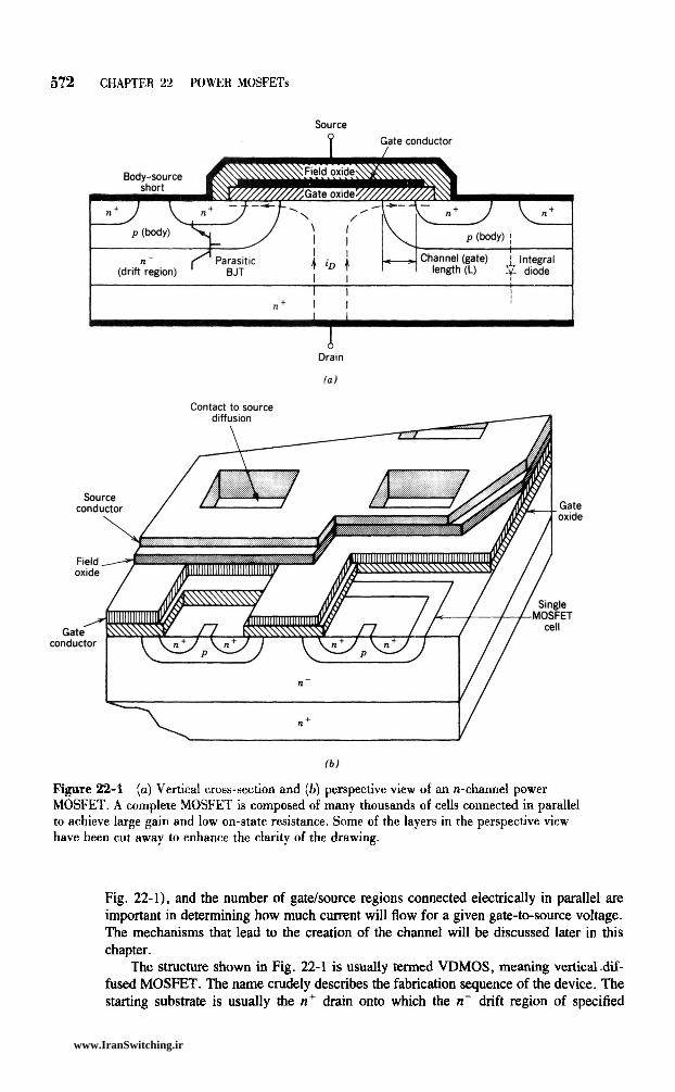

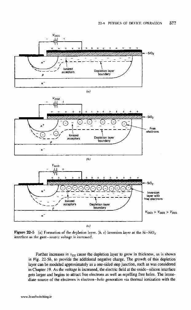
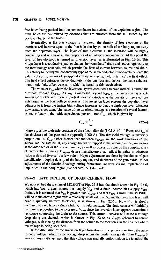
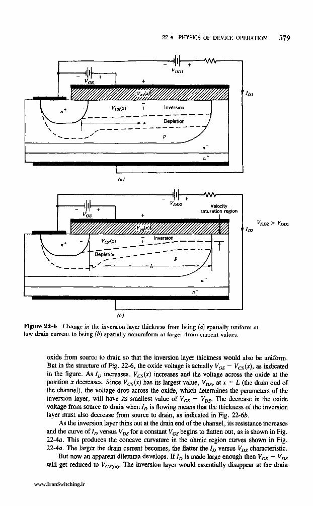
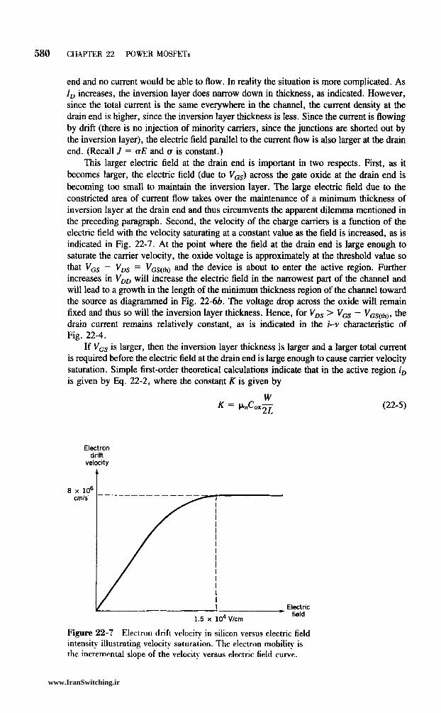
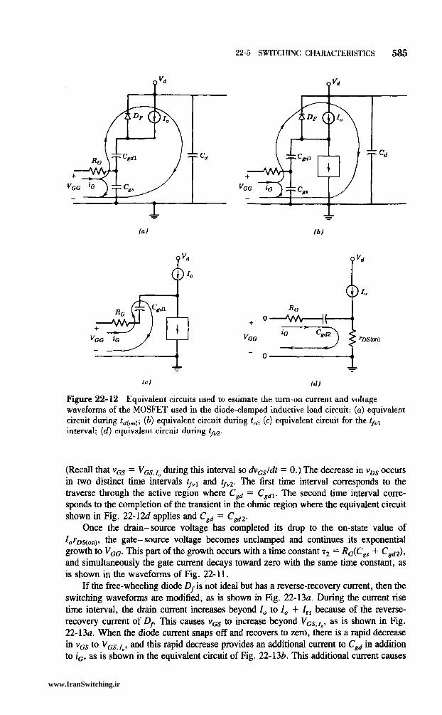
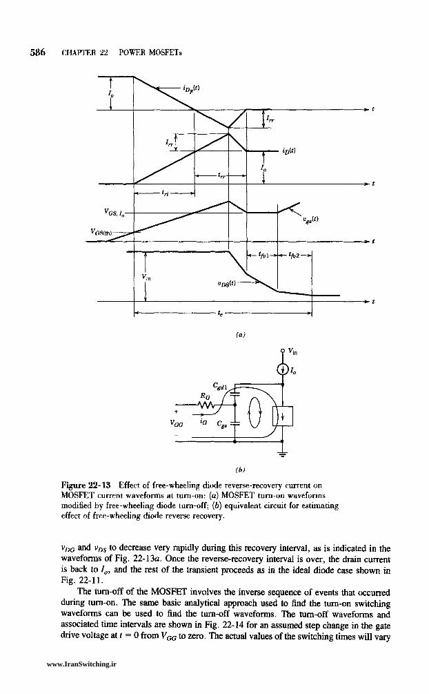
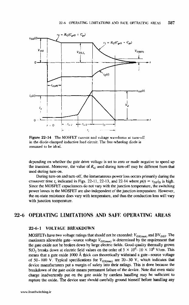
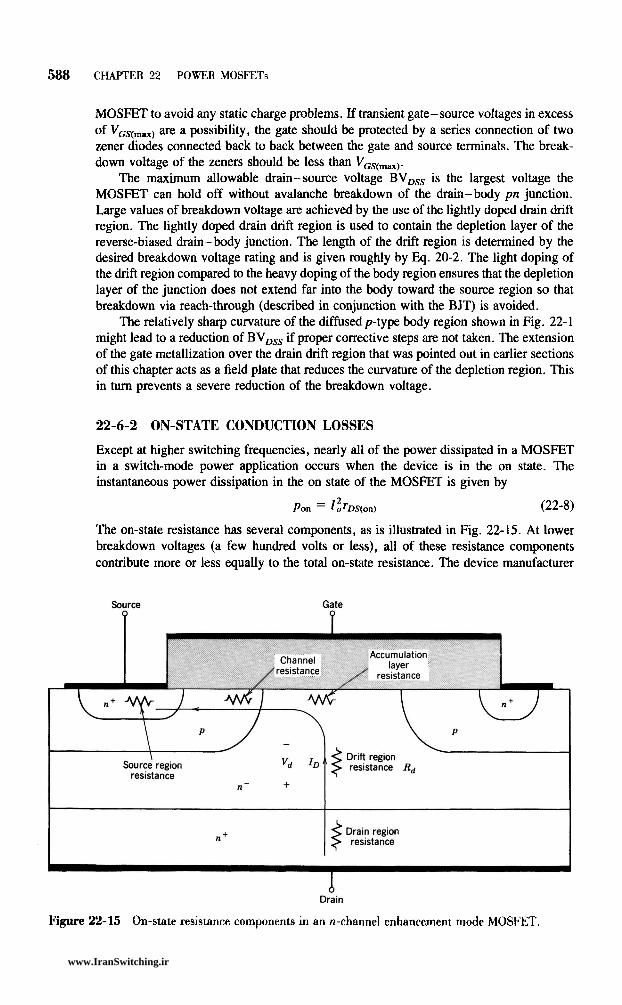
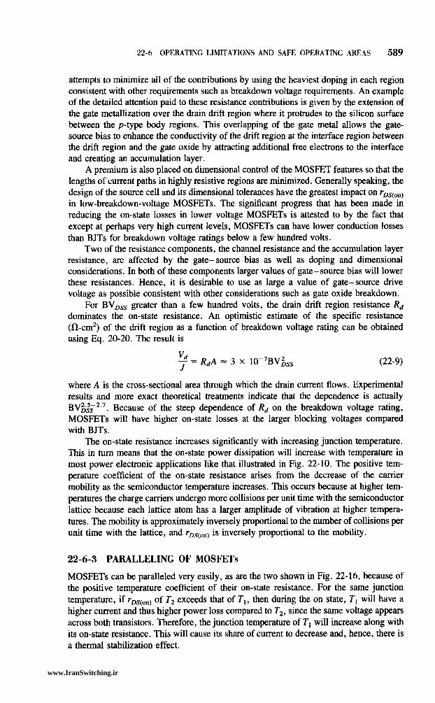
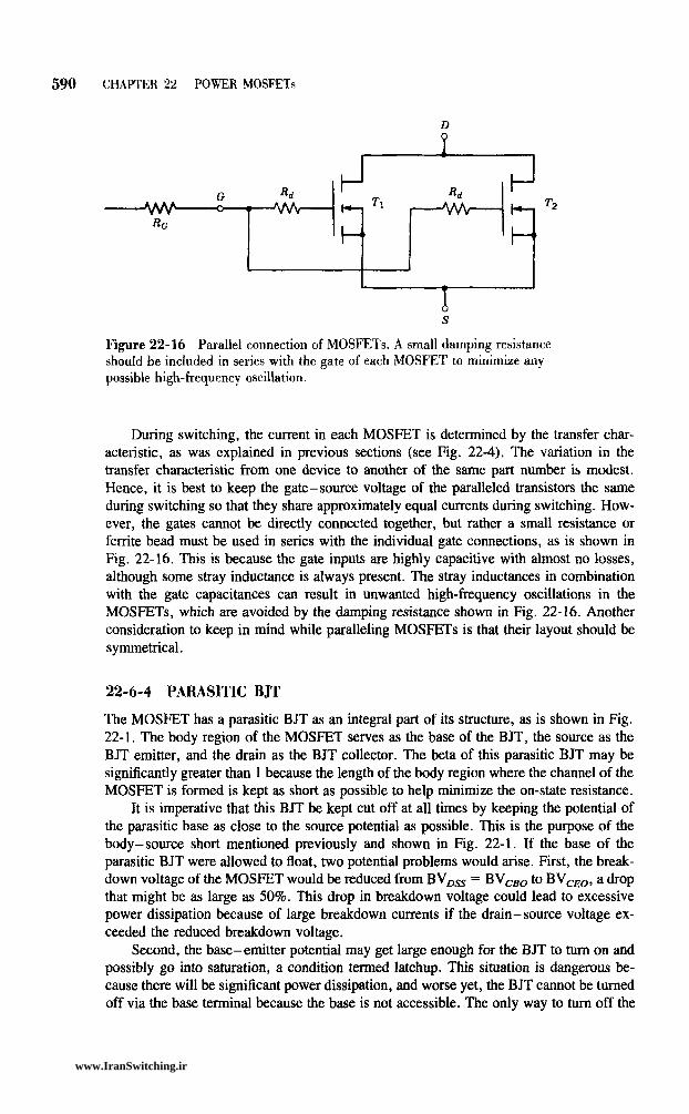
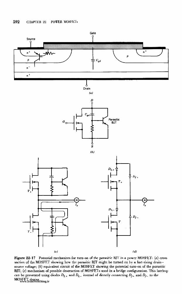


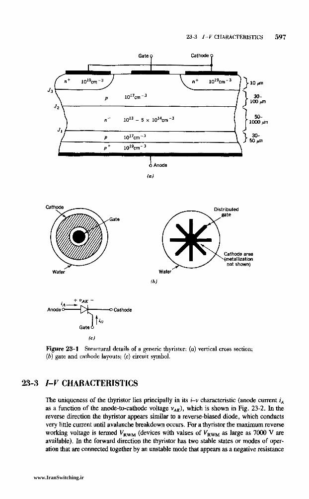
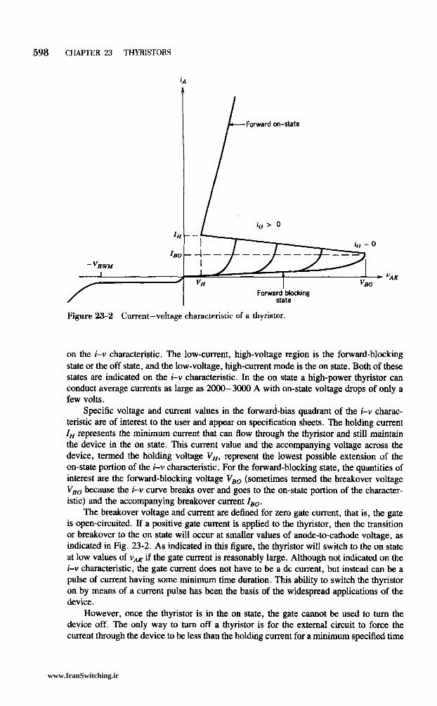
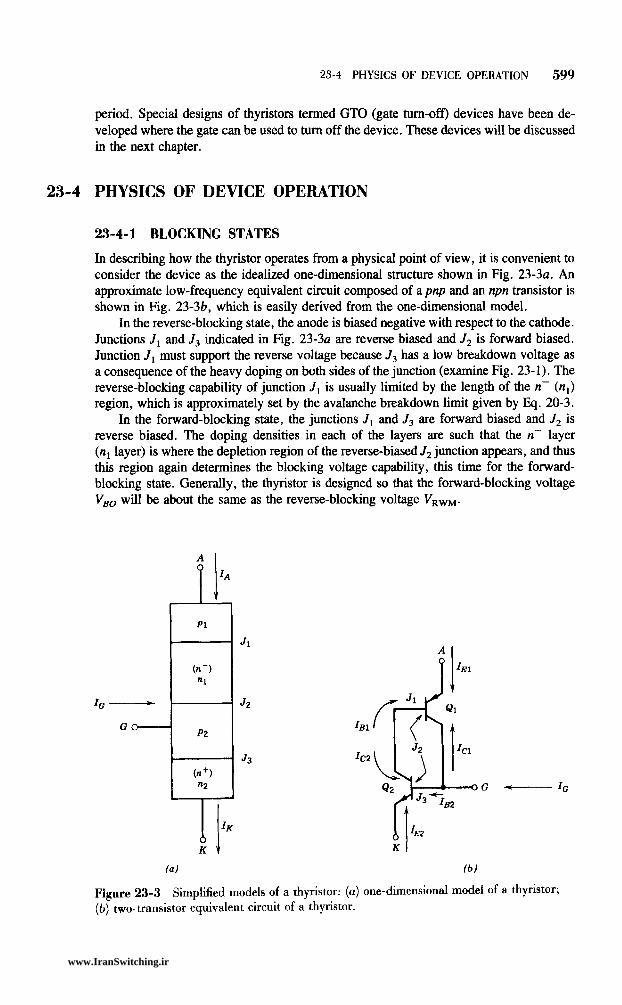
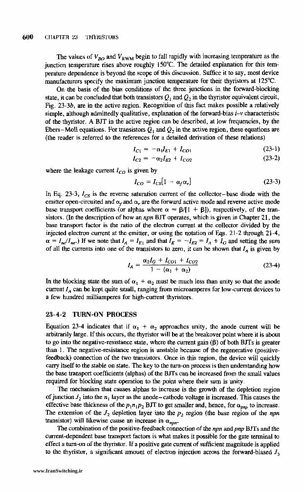
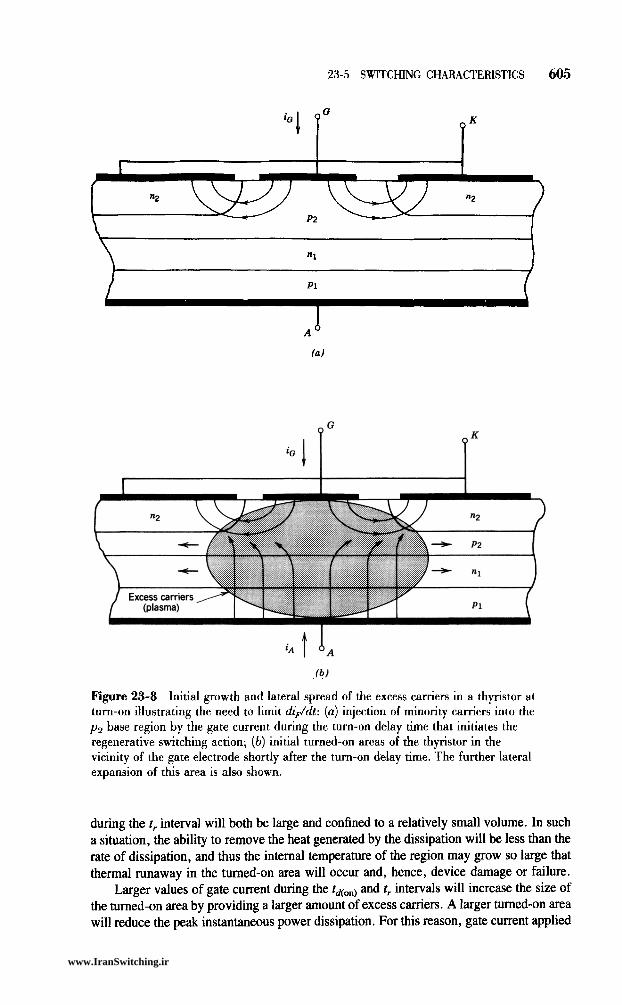
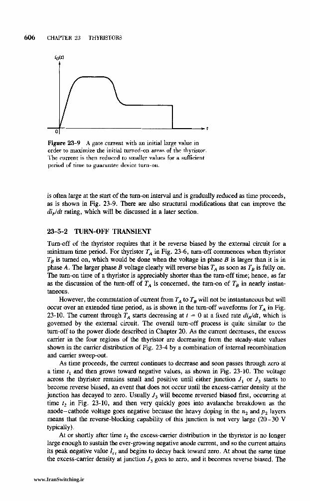
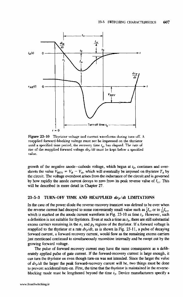
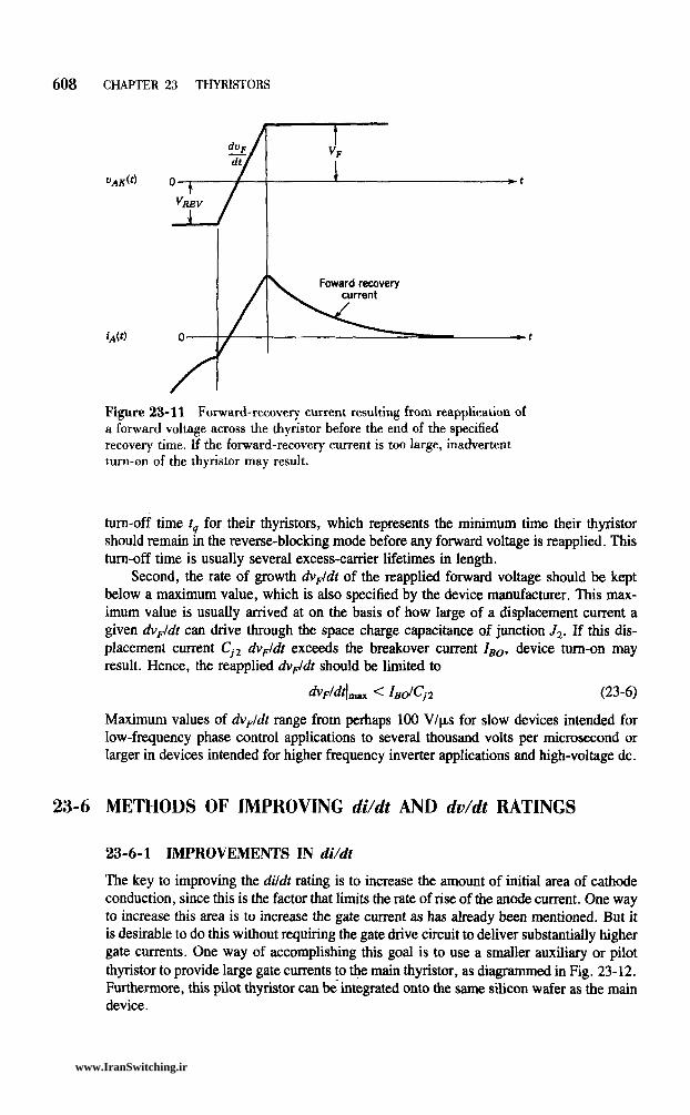
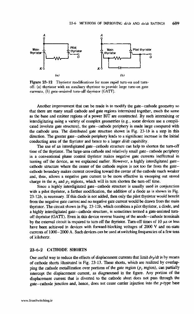
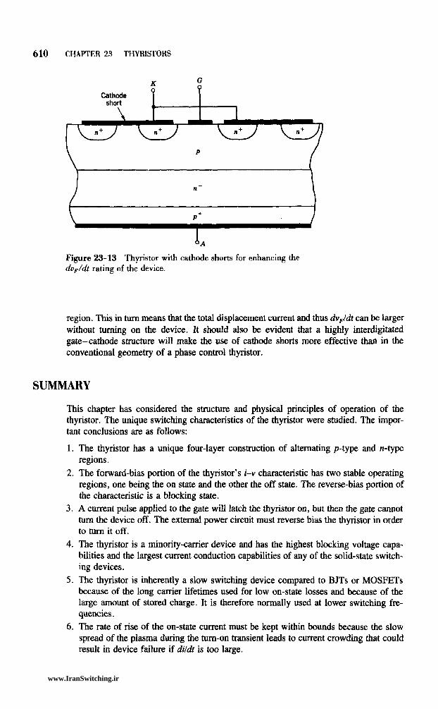


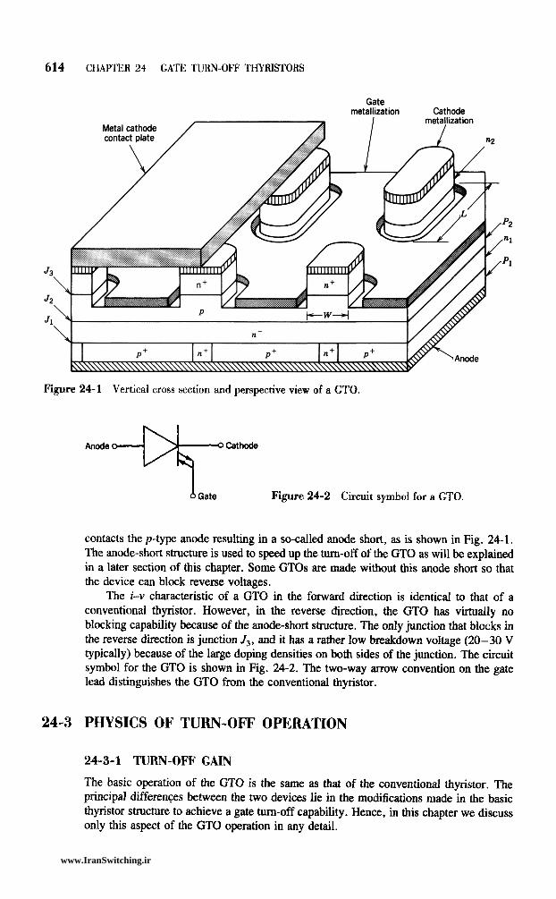
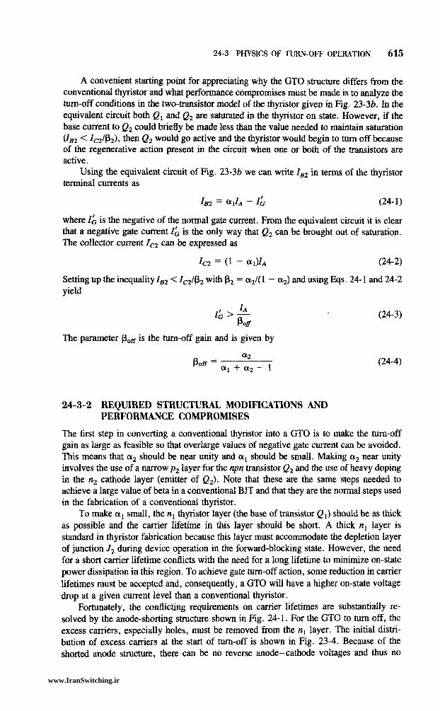
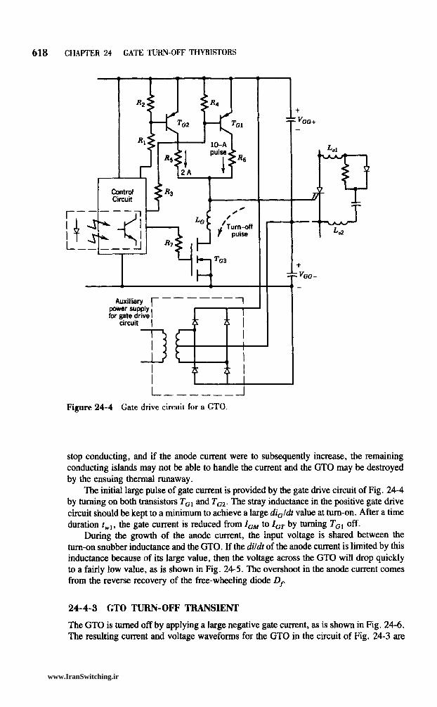
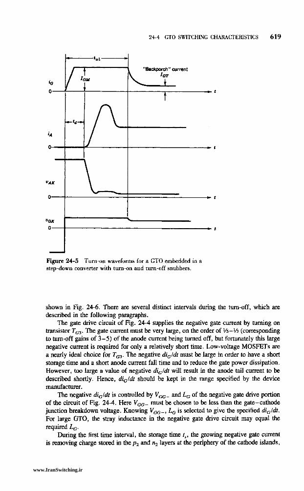
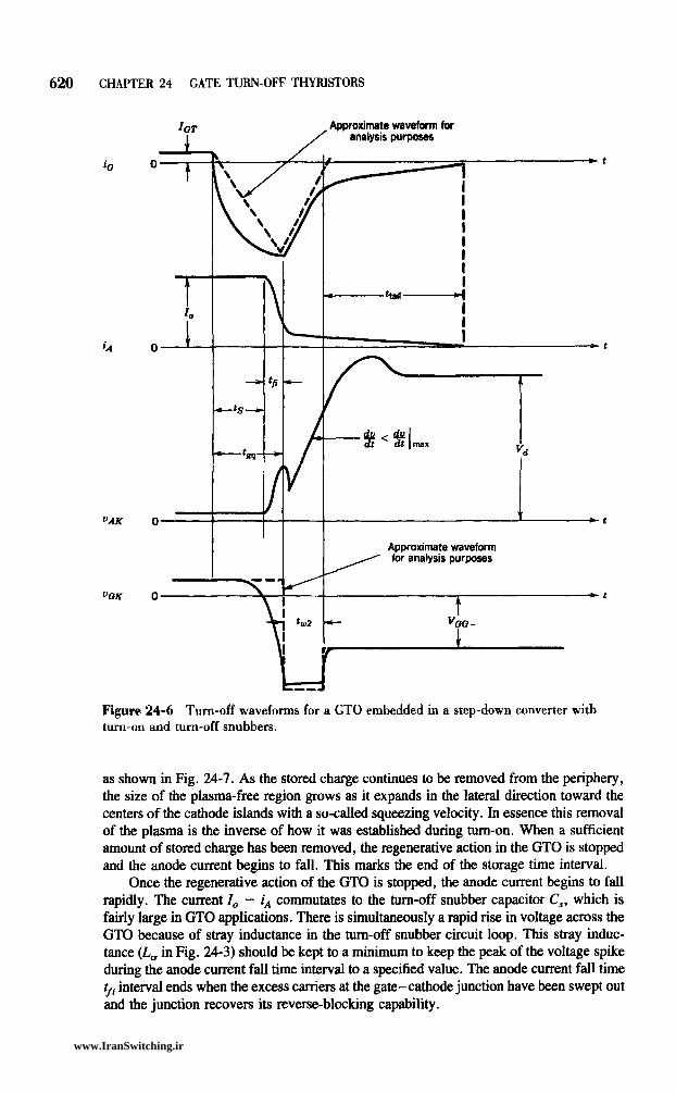
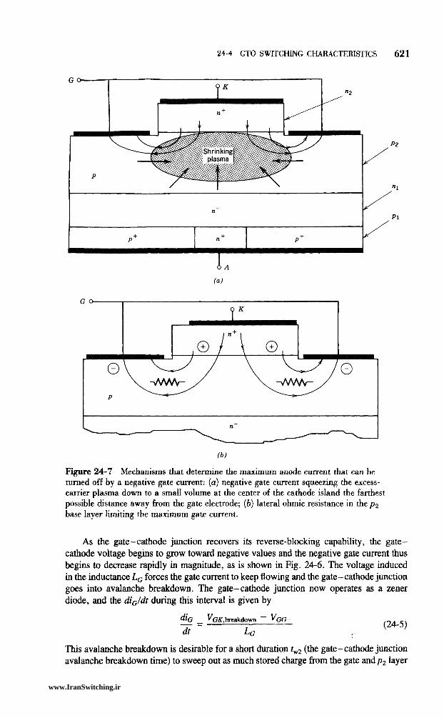
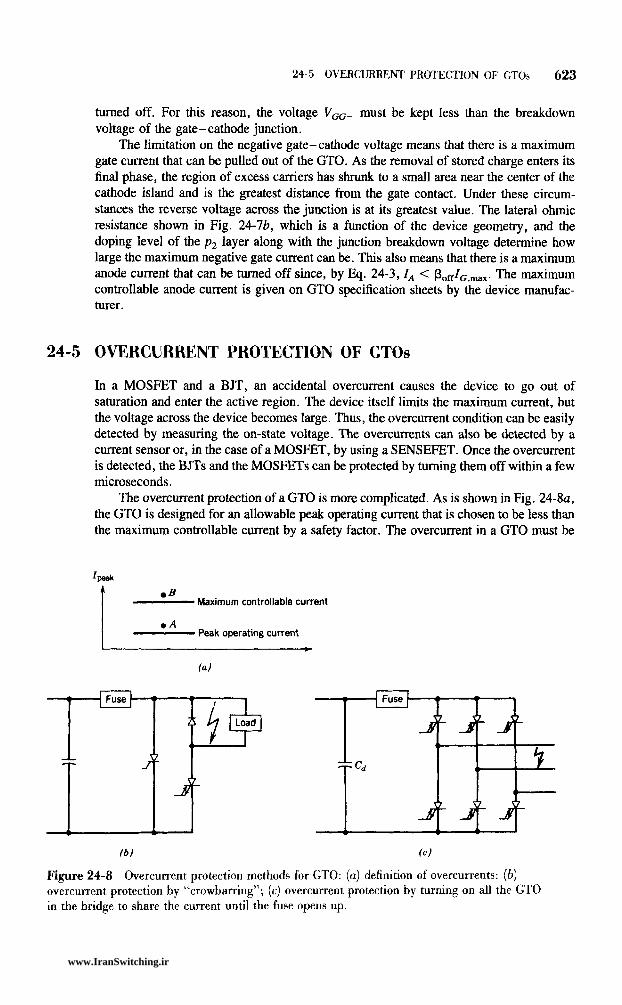


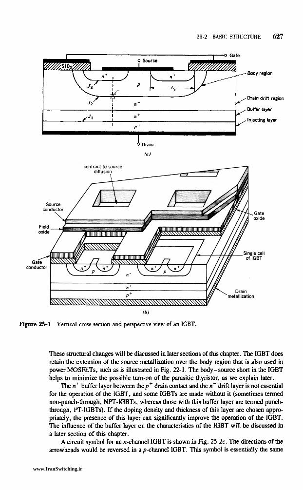
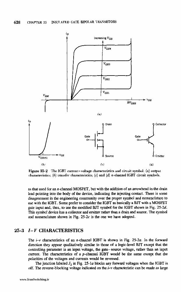

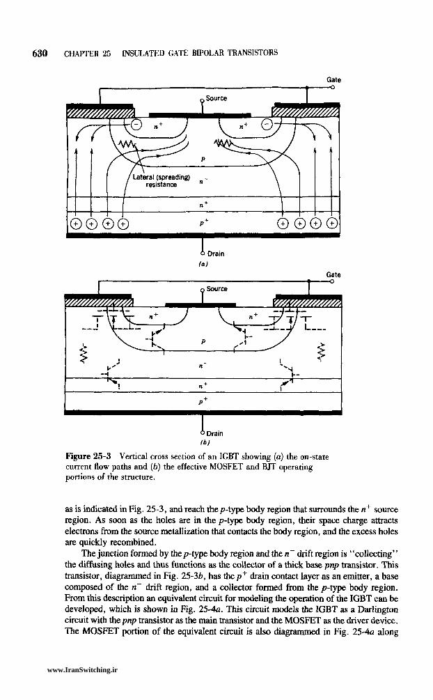
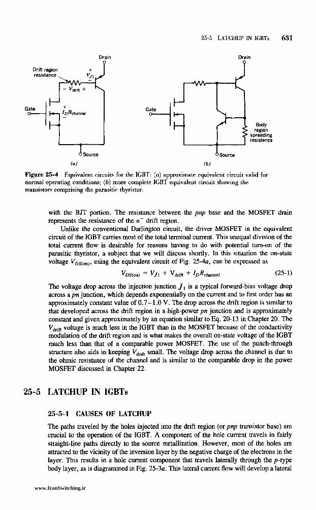
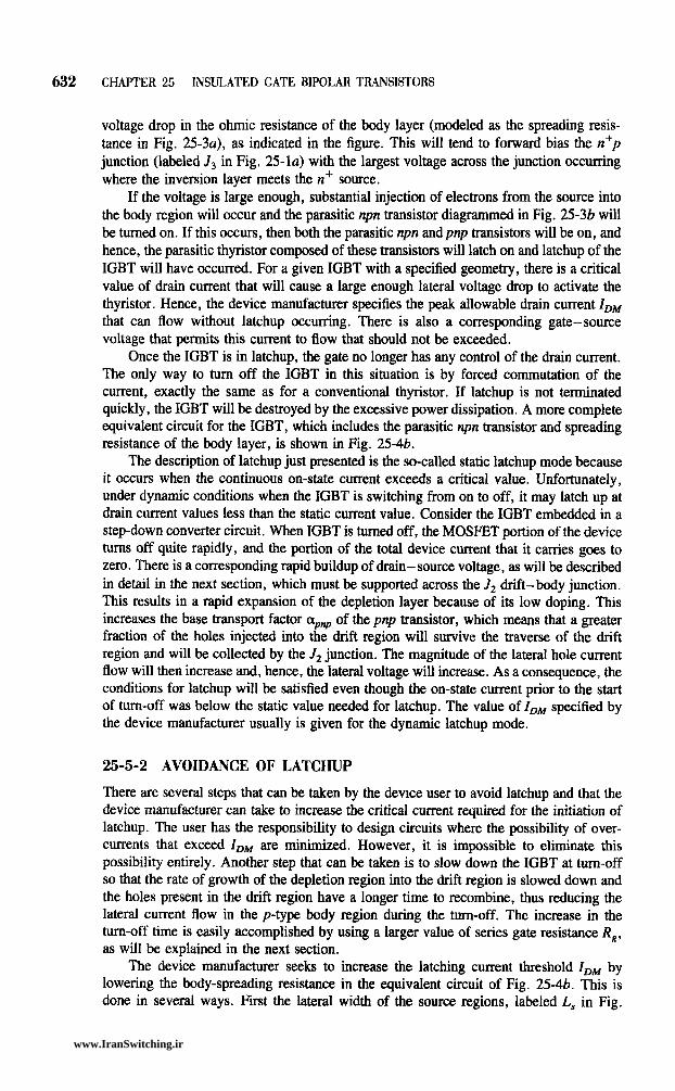
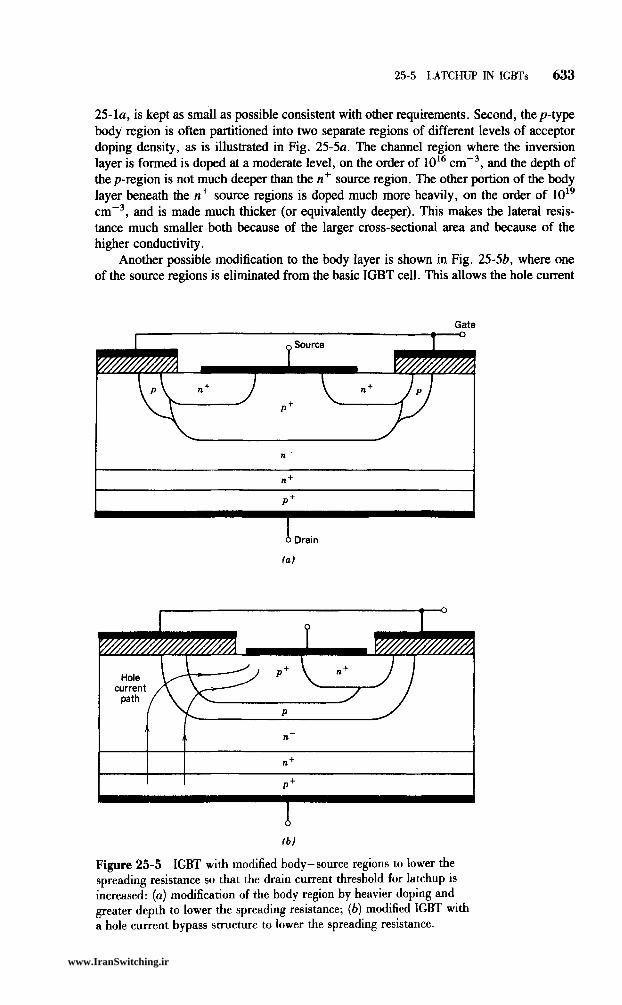
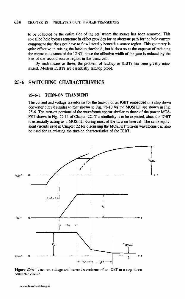
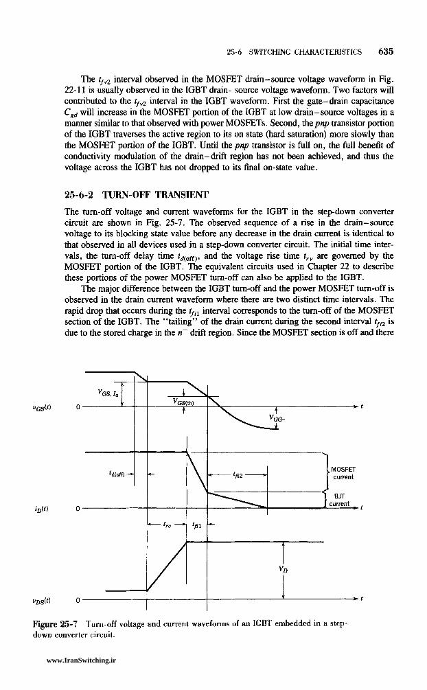

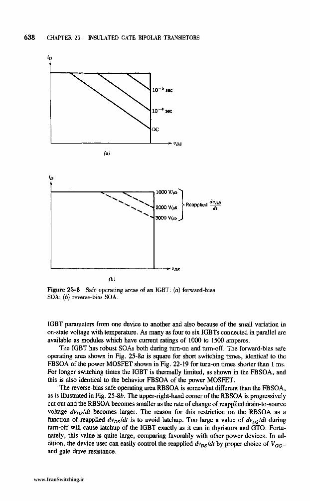


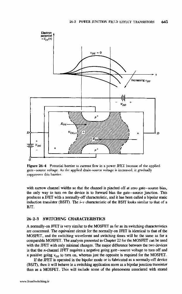
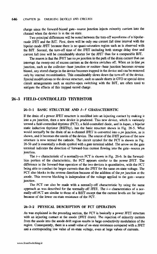
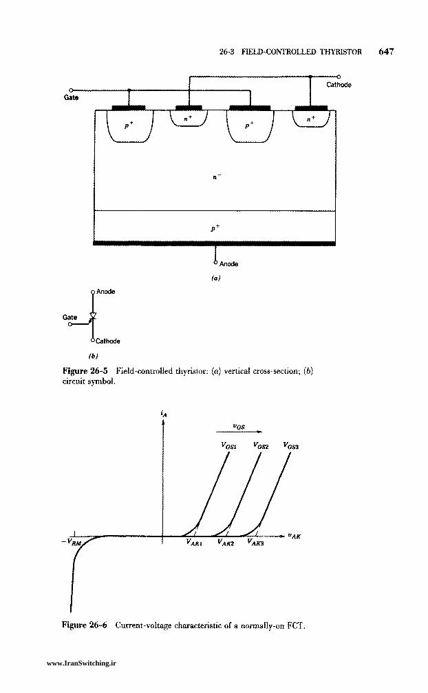
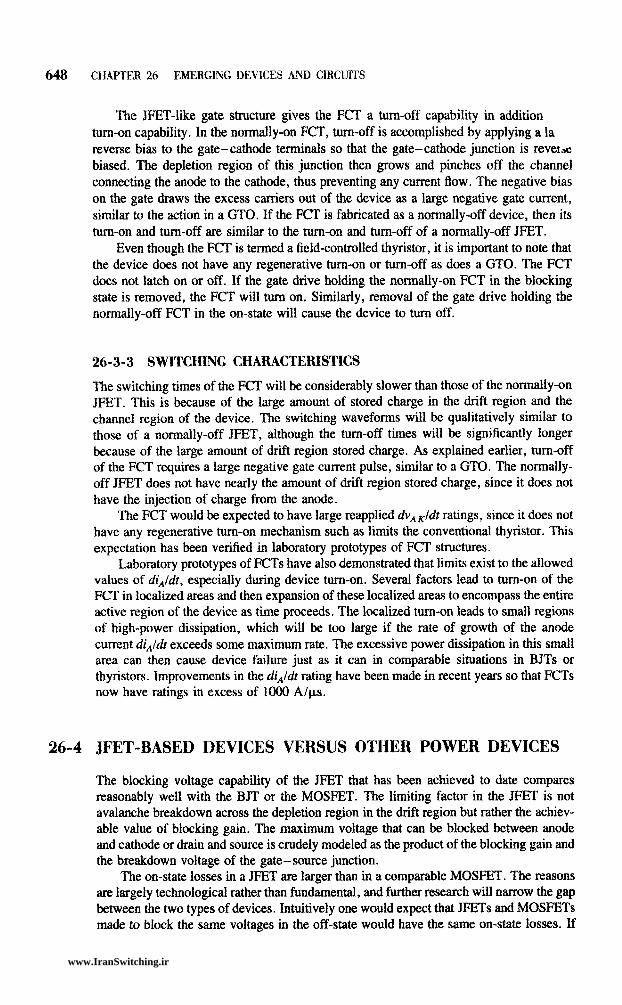

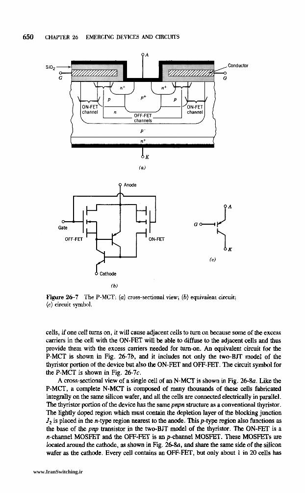
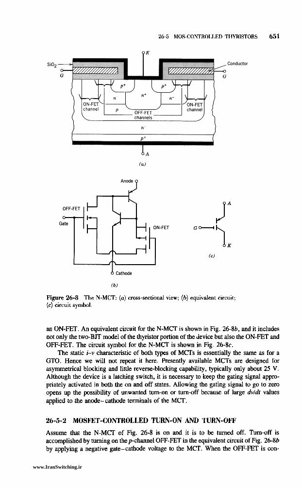

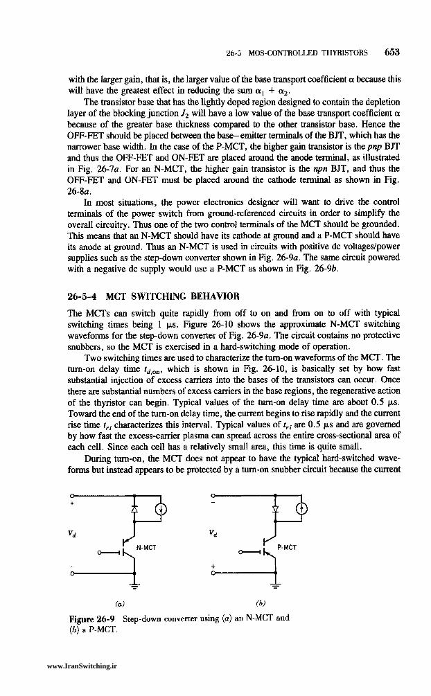
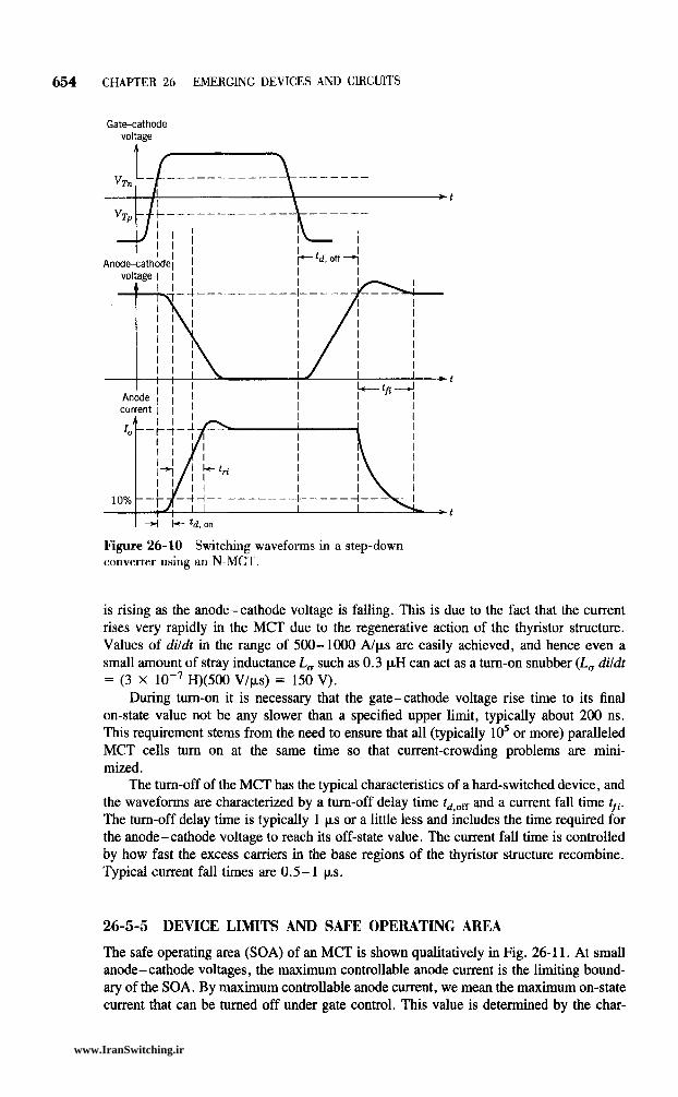
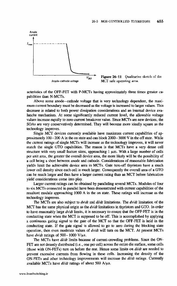
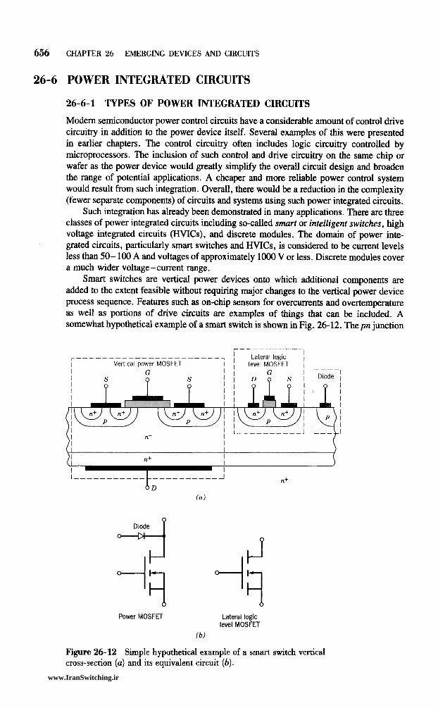
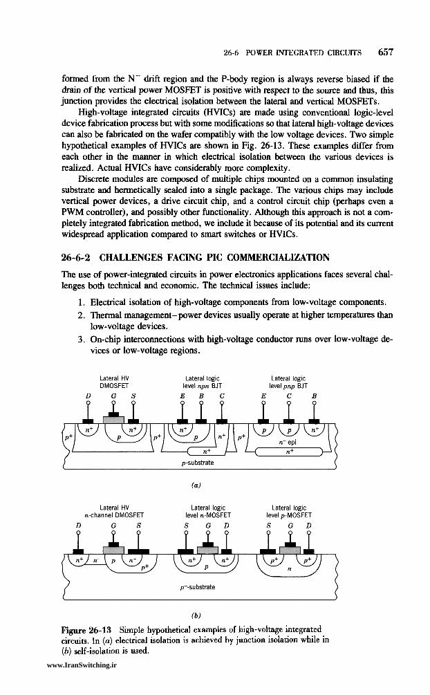
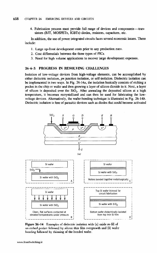
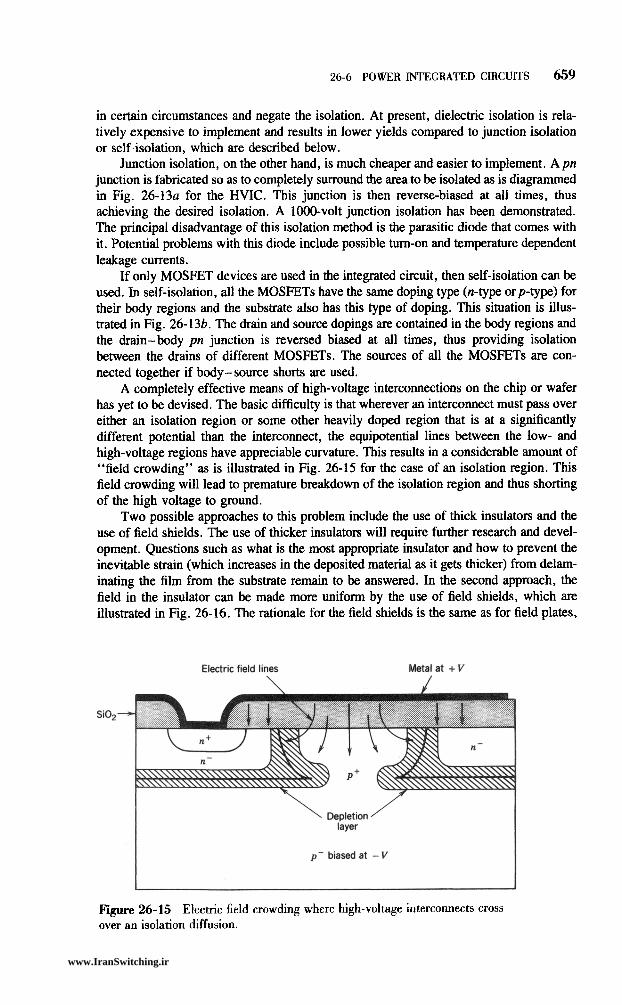

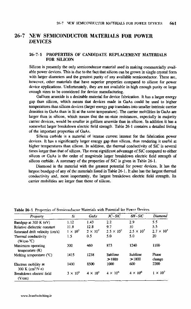
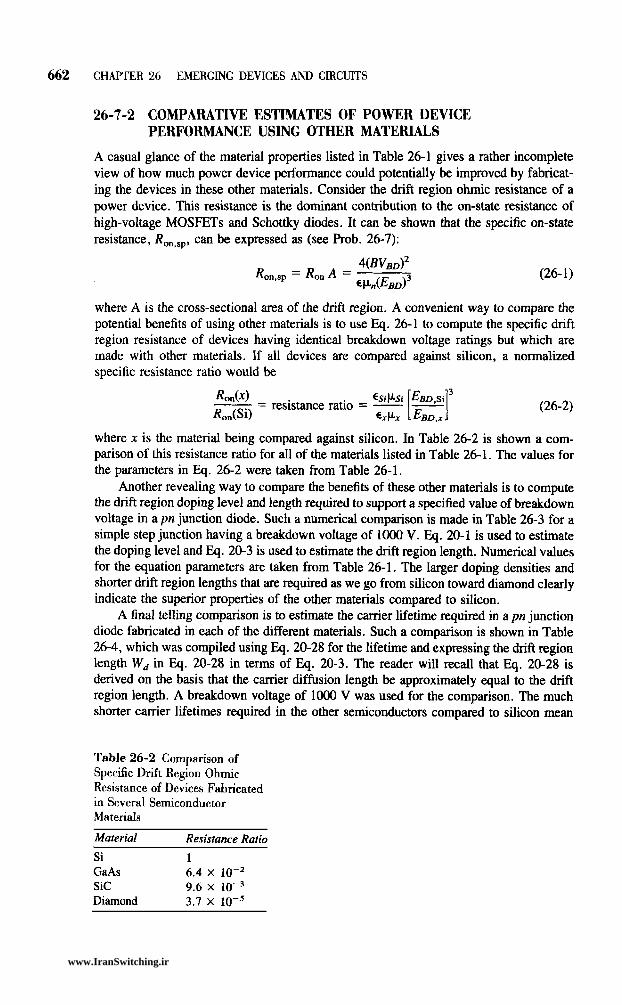


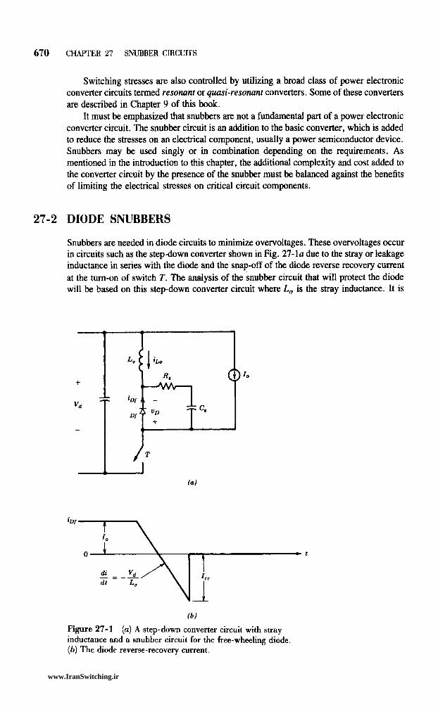
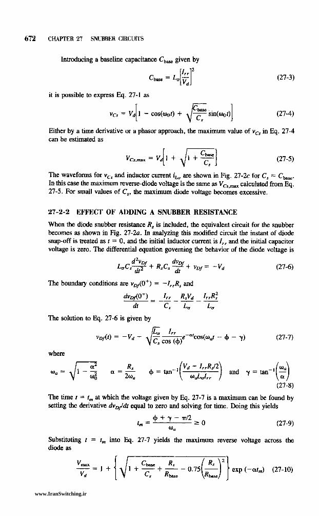
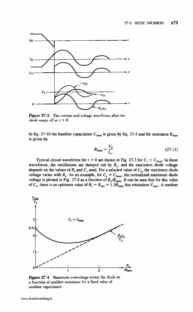
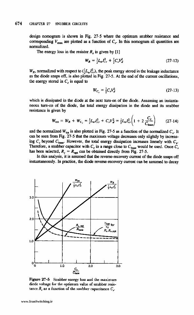
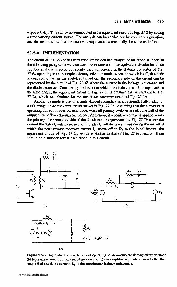
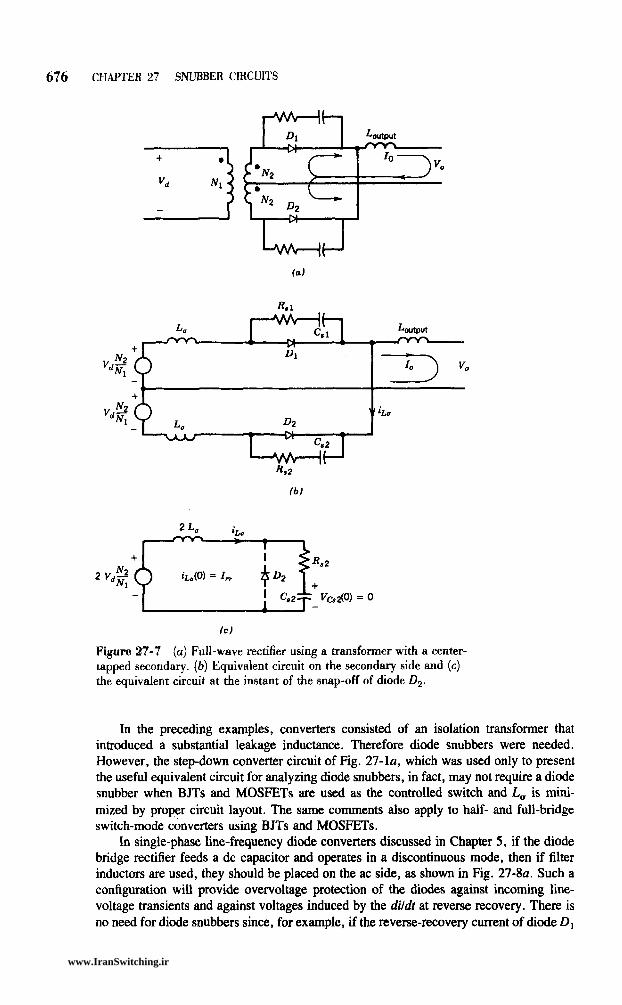
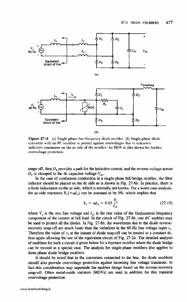
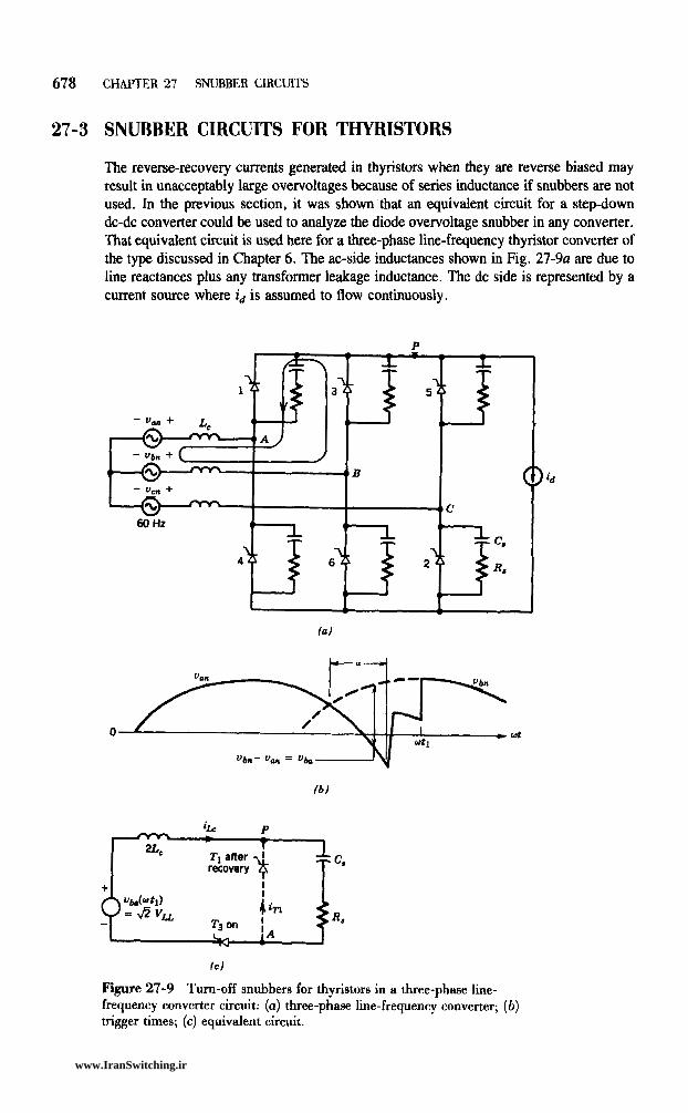
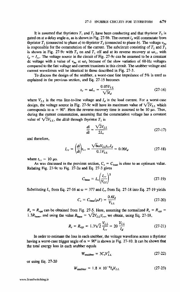
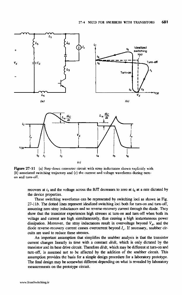
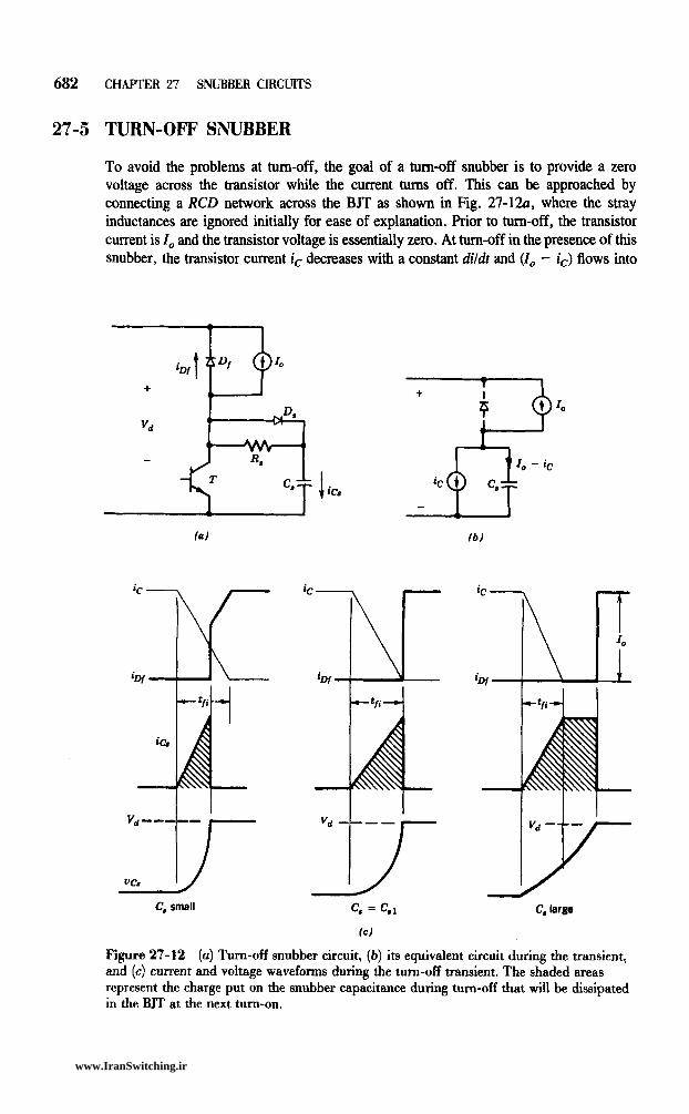
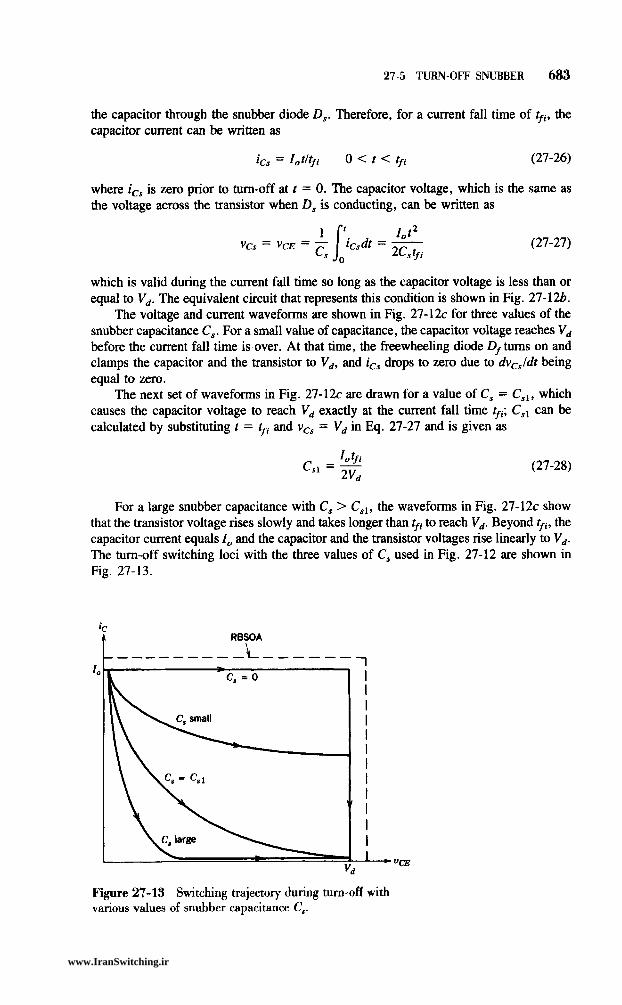
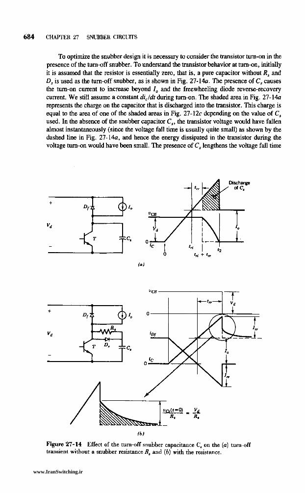


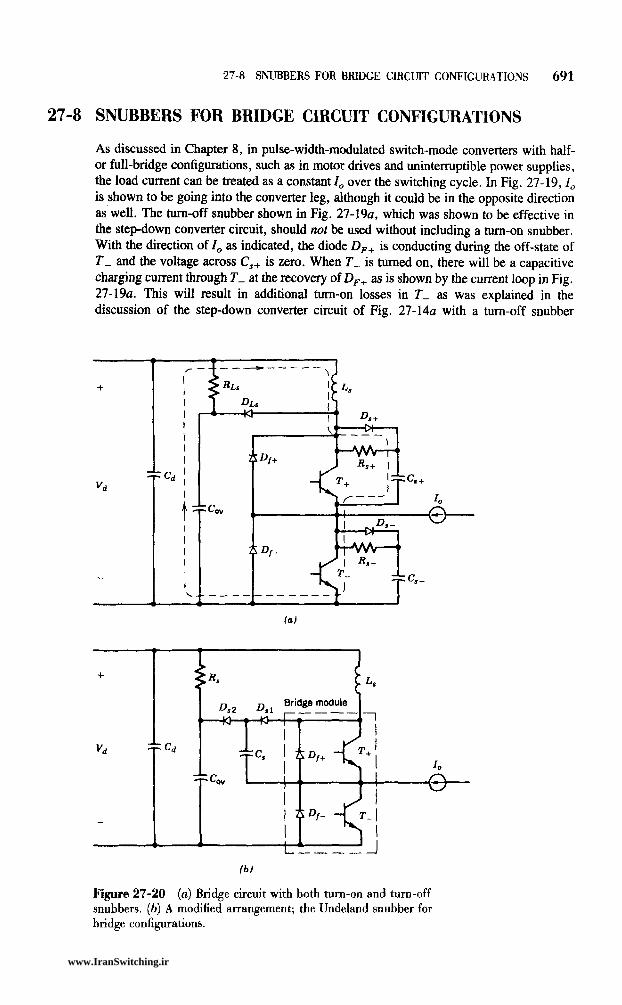


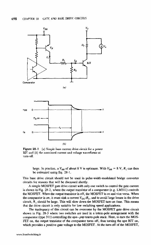
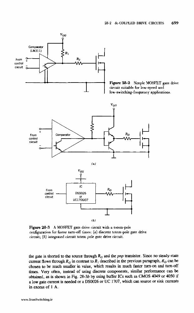
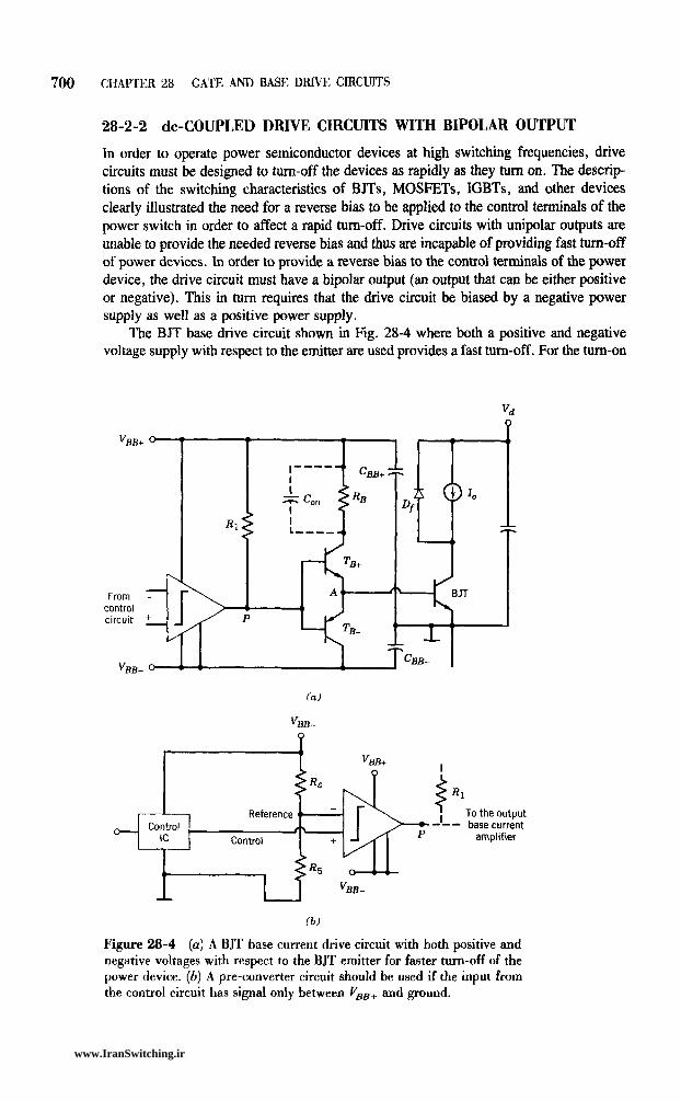
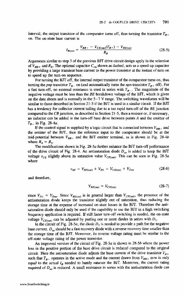
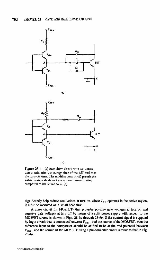
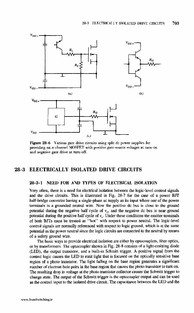
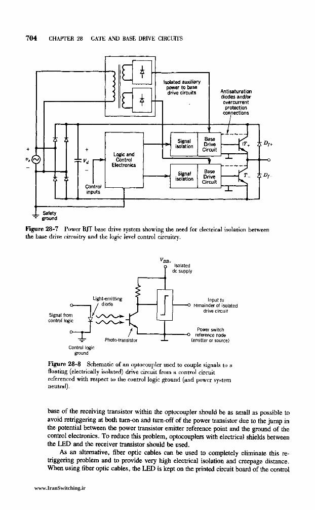
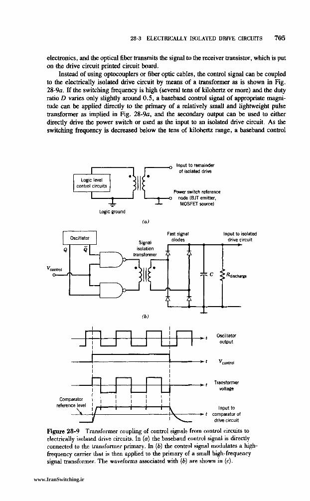
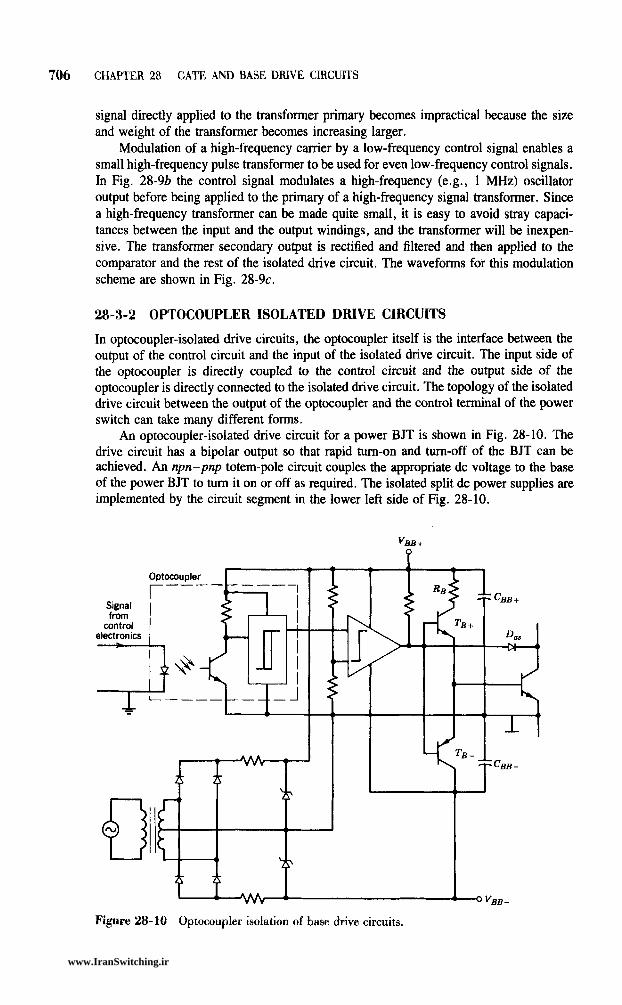
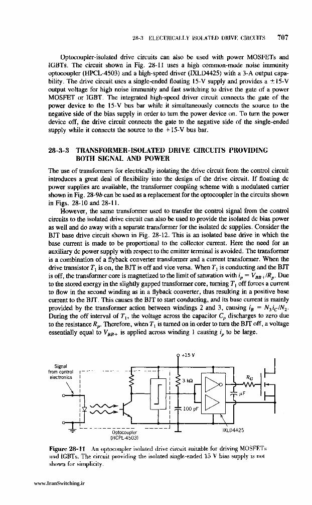
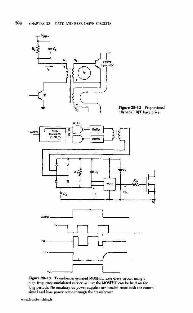
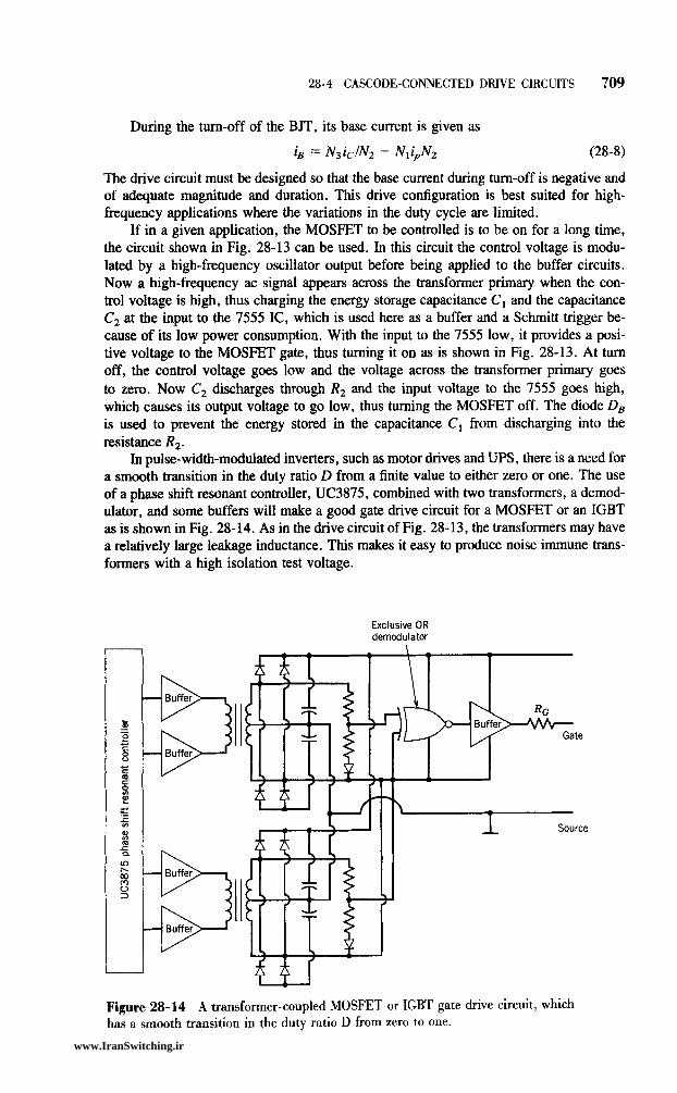
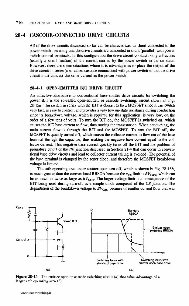
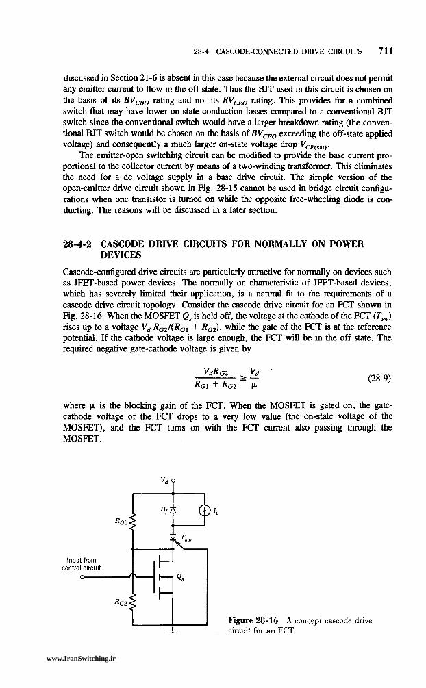
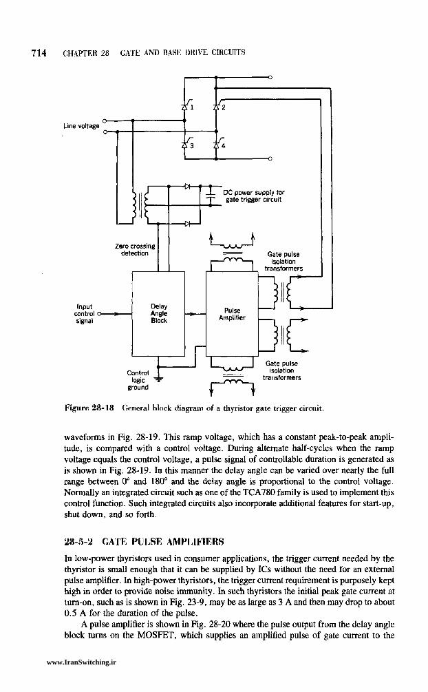
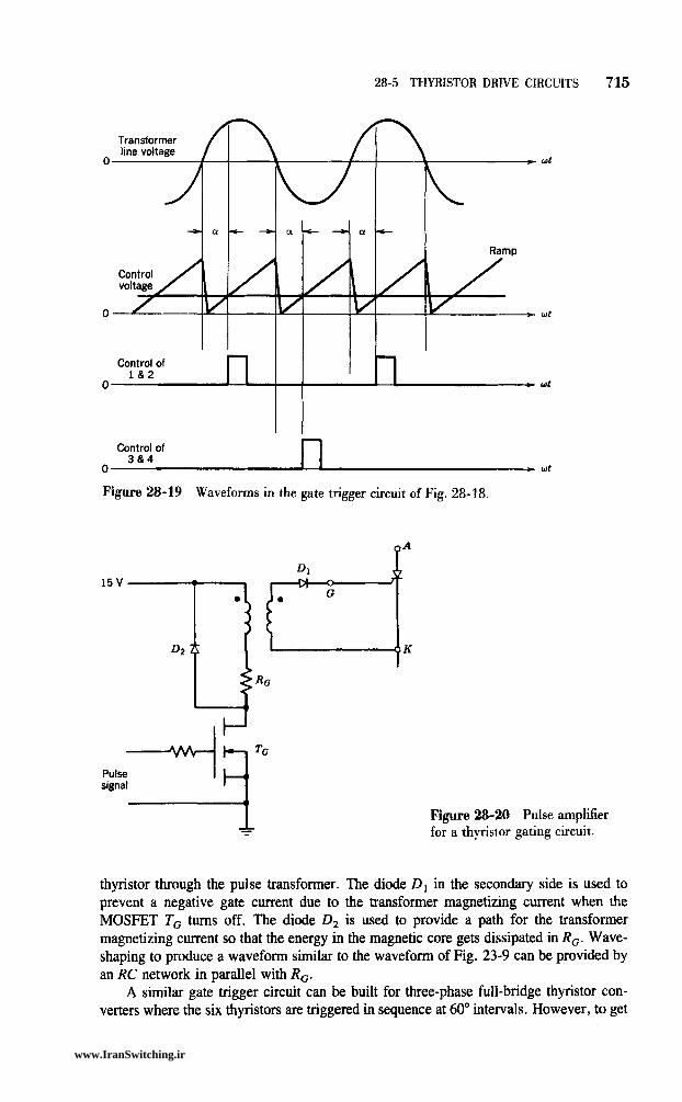
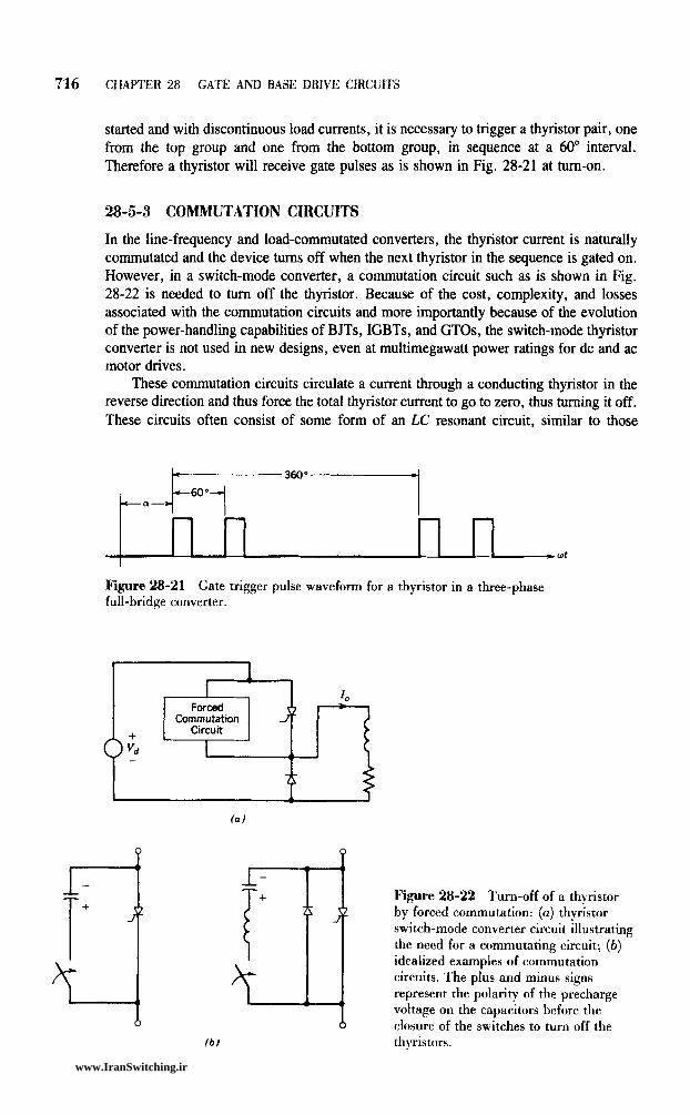
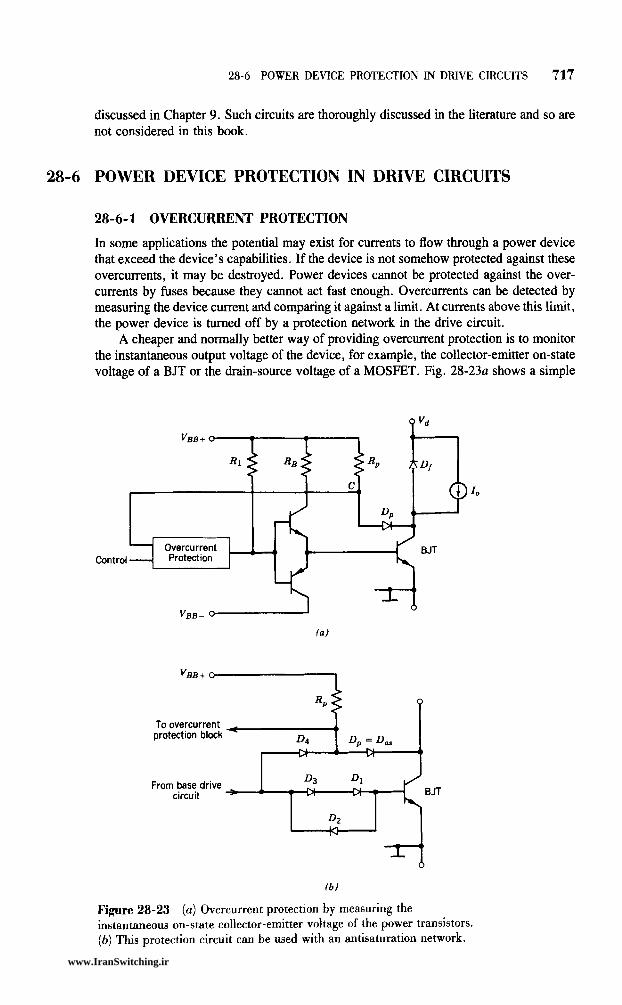
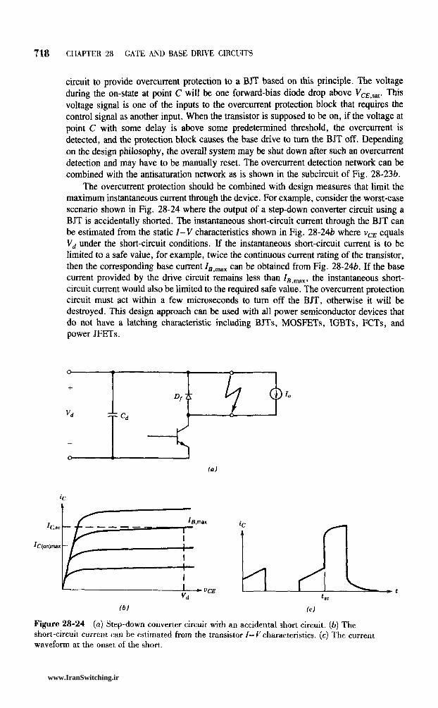

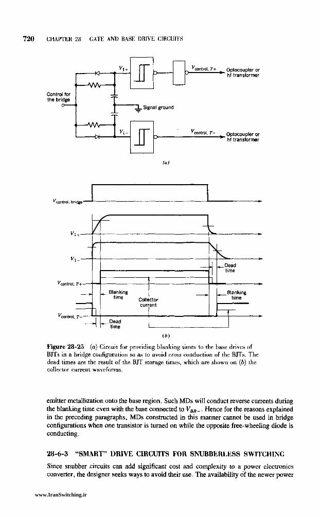
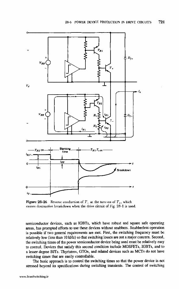
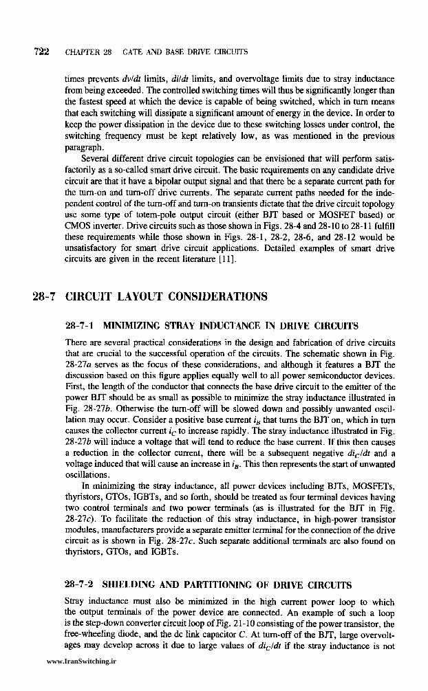
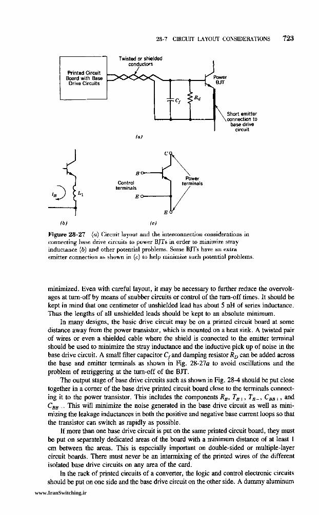
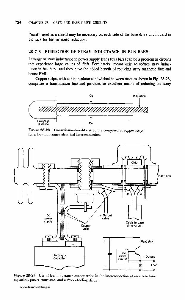
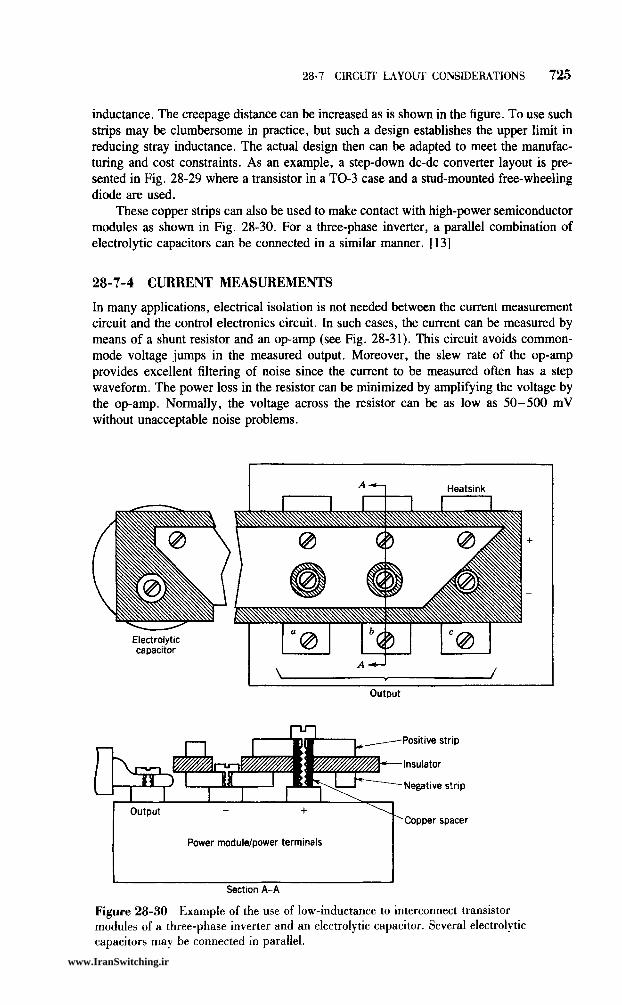
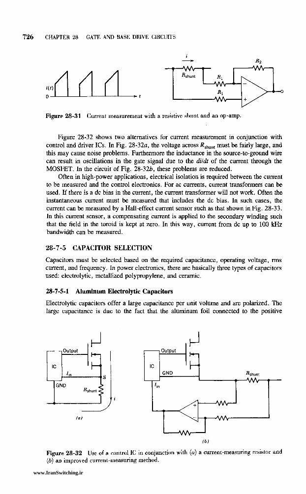
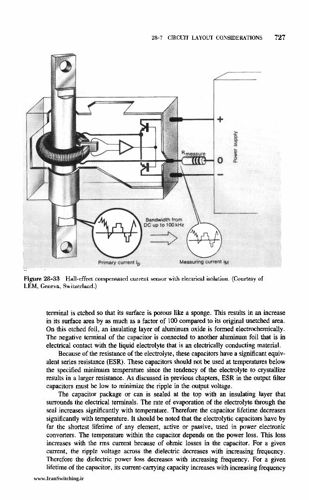

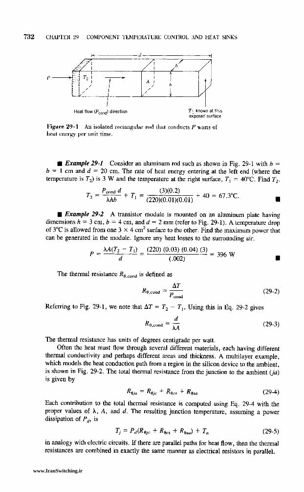
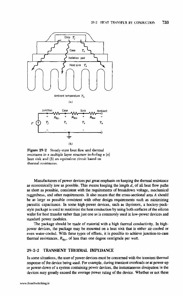
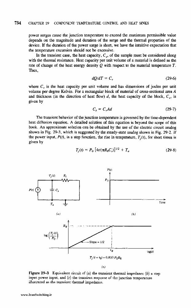
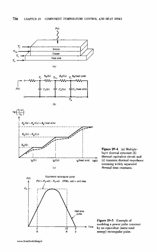

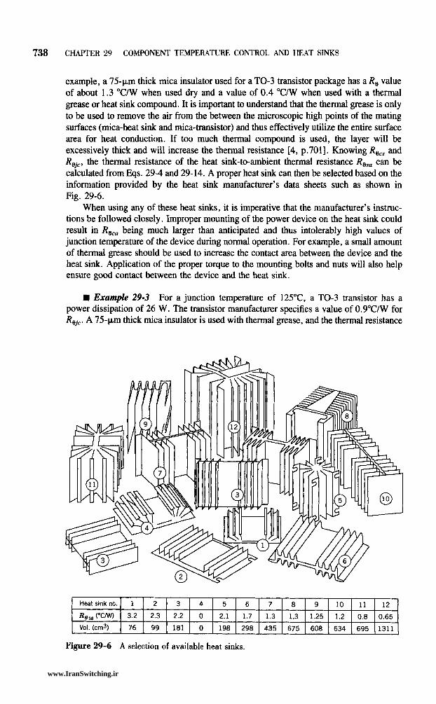


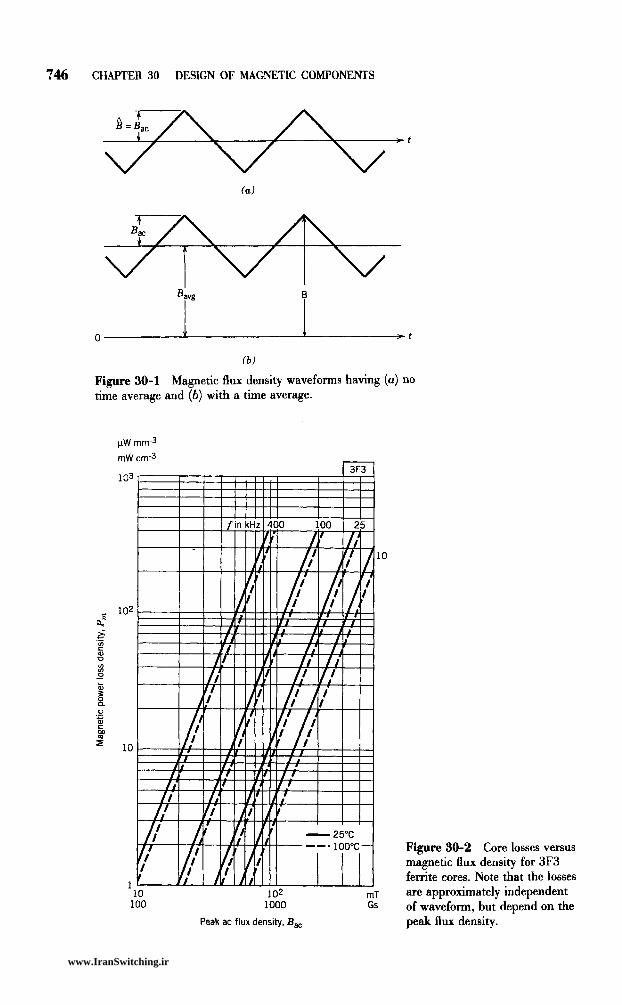
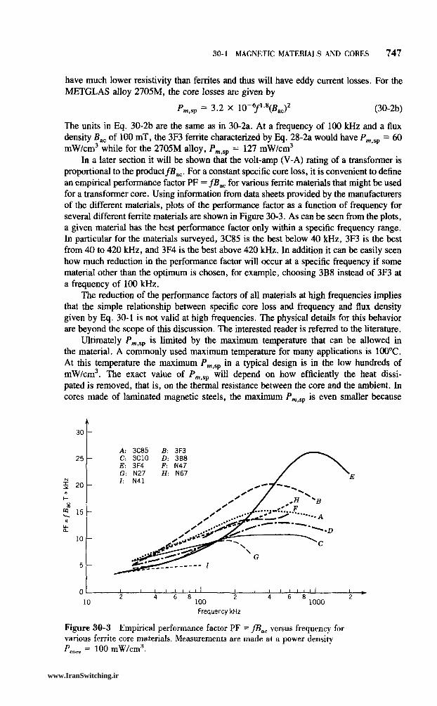
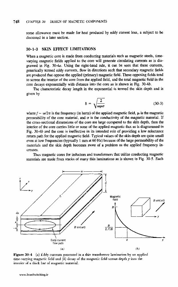
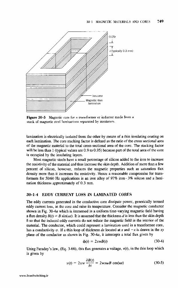
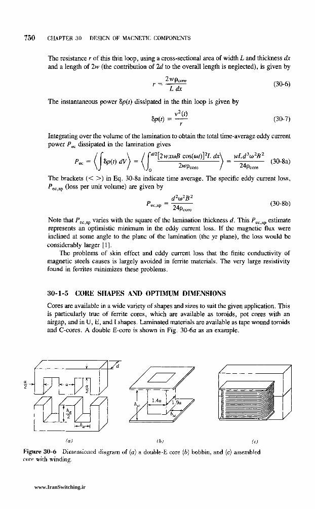

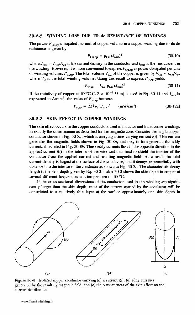


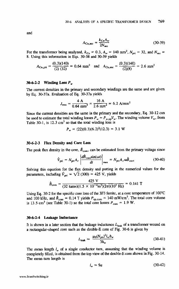
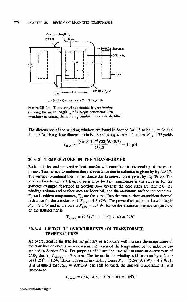
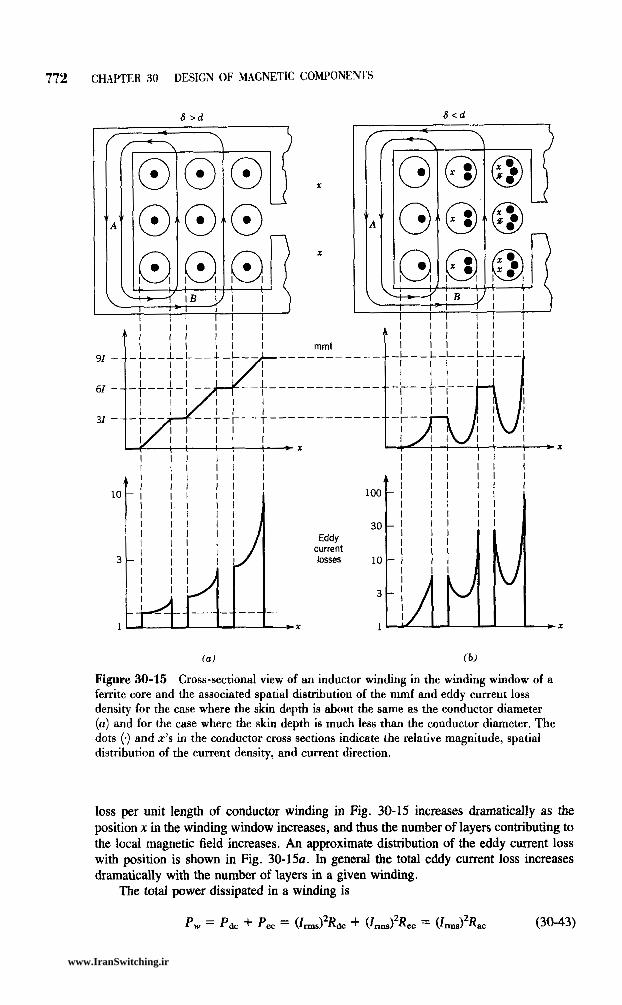
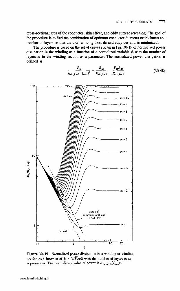
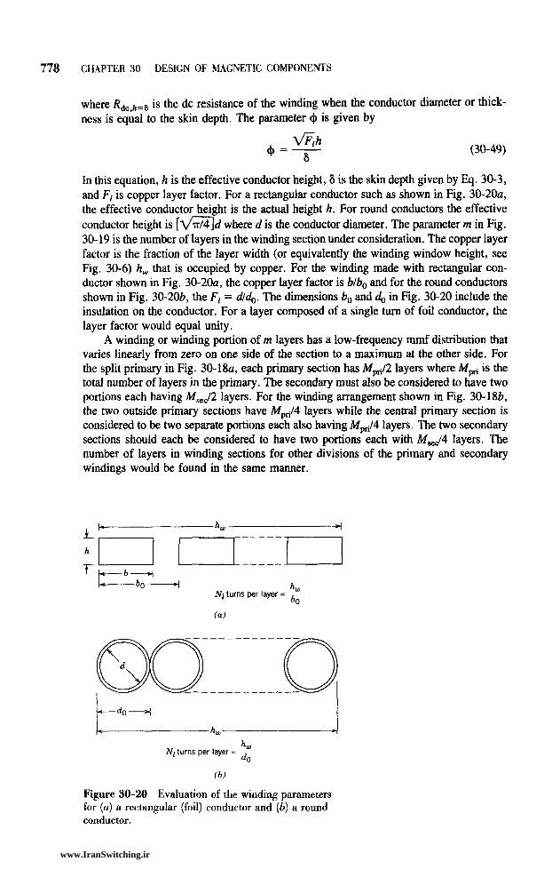
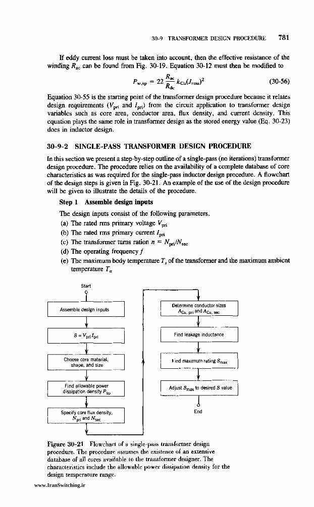
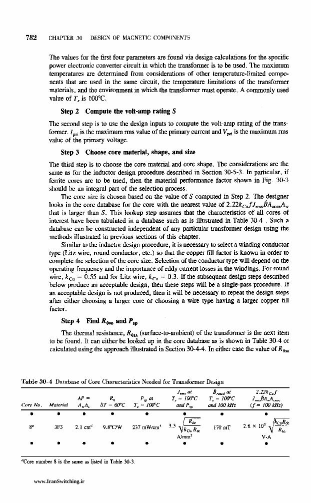


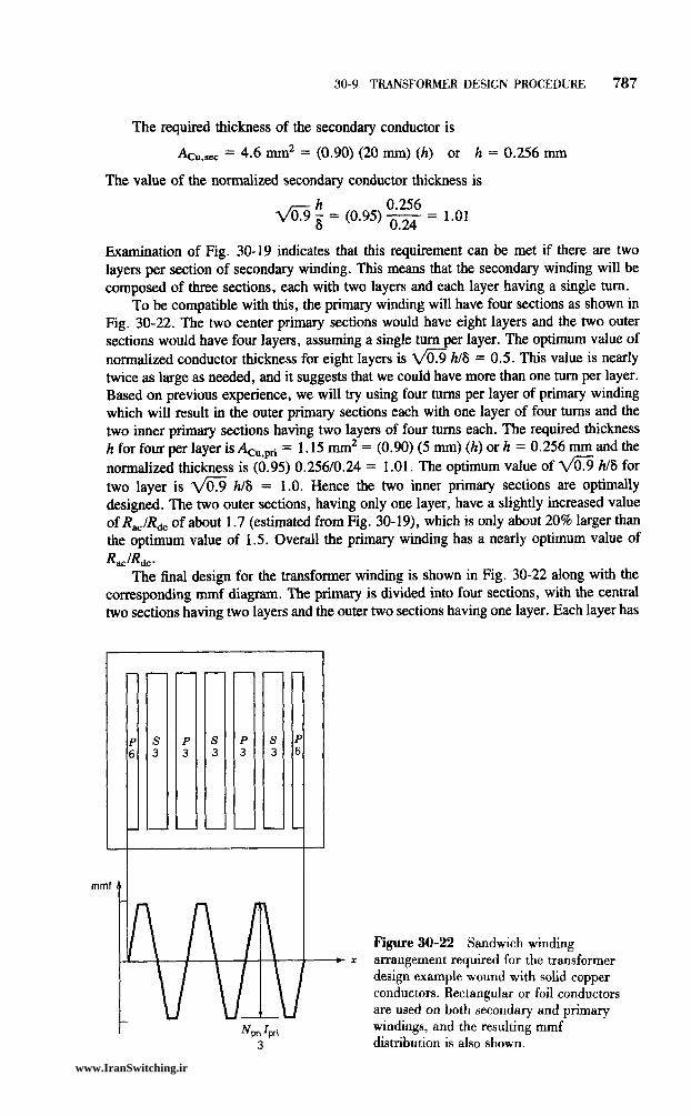
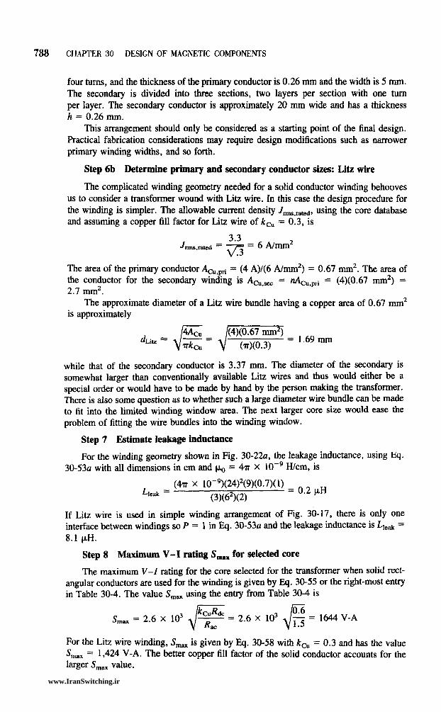


![PG Program [M. Tech. Electrical] Power Electronics ... - COEP](https://static.documents.pub/doc/80x56/6314172daca2b42b580d68bb/pg-program-m-tech-electrical-power-electronics-coep.jpg)
