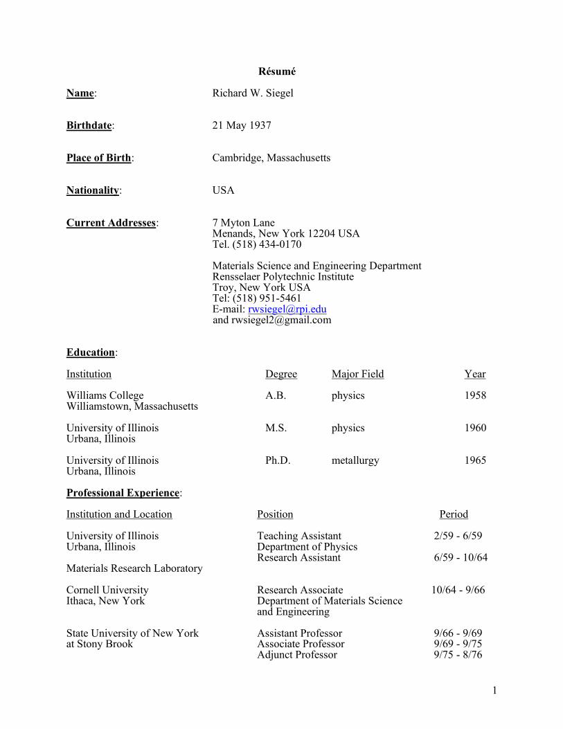
1 Résumé Name: Richard W. Siegel Birthdate: 21 May 1937 Place of Birth: Cambridge, Massachusetts Nationality: USA Current Addresses: 7 Myton Lane Menands, New York 12204 USA Tel. (518) 434-0170 Materials Science and Engineering Department Rensselaer Polytechnic Institute Troy, New York USA Tel: (518) 951-5461 E-mail: [email protected]and [email protected]Education: Institution Degree Major Field Year Williams College A.B. physics 1958 Williamstown, Massachusetts University of Illinois M.S. physics 1960 Urbana, Illinois University of Illinois Ph.D. metallurgy 1965 Urbana, Illinois Professional Experience: Institution and Location Position Period University of Illinois Teaching Assistant 2/59 - 6/59 Urbana, Illinois Department of Physics Research Assistant 6/59 - 10/64 Materials Research Laboratory Cornell University Research Associate 10/64 - 9/66 Ithaca, New York Department of Materials Science and Engineering State University of New York Assistant Professor 9/66 - 9/69 at Stony Brook Associate Professor 9/69 - 9/75 Adjunct Professor 9/75 - 8/76
Transcript
1
Résumé Name: Richard W. Siegel Birthdate: 21 May 1937 Place of Birth: Cambridge, Massachusetts Nationality: USA Current Addresses: 7 Myton Lane Menands, New York 12204 USA Tel. (518) 434-0170 Materials Science and Engineering Department Rensselaer Polytechnic Institute Troy, New York USA Tel: (518) 951-5461 E-mail: [email protected] and [email protected] Education: Institution Degree Major Field Year Williams College A.B. physics 1958 Williamstown, Massachusetts University of Illinois M.S. physics 1960 Urbana, Illinois University of Illinois Ph.D. metallurgy 1965 Urbana, Illinois Professional Experience: Institution and Location Position Period University of Illinois Teaching Assistant 2/59 - 6/59 Urbana, Illinois Department of Physics Research Assistant 6/59 - 10/64 Materials Research Laboratory Cornell University Research Associate 10/64 - 9/66 Ithaca, New York Department of Materials Science and Engineering State University of New York Assistant Professor 9/66 - 9/69 at Stony Brook Associate Professor 9/69 - 9/75 Adjunct Professor 9/75 - 8/76
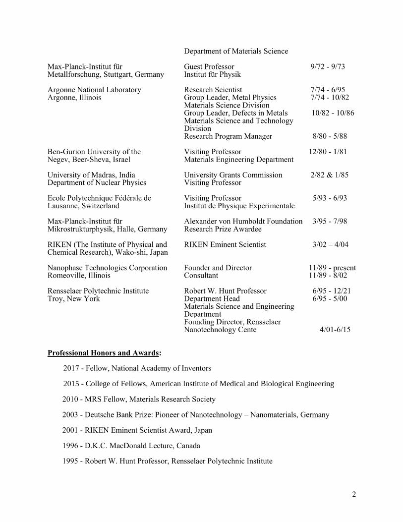
Department of Materials Science Max-Planck-Institut für Guest Professor 9/72 - 9/73 Metallforschung, Stuttgart, Germany Institut für Physik Argonne National Laboratory Research Scientist 7/74 - 6/95 Argonne, Illinois Group Leader, Metal Physics 7/74 - 10/82 Materials Science Division Group Leader, Defects in Metals 10/82 - 10/86 Materials Science and Technology Division Research Program Manager 8/80 - 5/88 Ben-Gurion University of the Visiting Professor 12/80 - 1/81 Negev, Beer-Sheva, Israel Materials Engineering Department University of Madras, India University Grants Commission 2/82 & 1/85 Department of Nuclear Physics Visiting Professor Ecole Polytechnique Fédérale de Visiting Professor 5/93 - 6/93 Lausanne, Switzerland Institut de Physique Experimentale Max-Planck-Institut für Alexander von Humboldt Foundation 3/95 - 7/98 Mikrostrukturphysik, Halle, Germany Research Prize Awardee RIKEN (The Institute of Physical and RIKEN Eminent Scientist 3/02 – 4/04 Chemical Research), Wako-shi, Japan Nanophase Technologies Corporation Founder and Director 11/89 - present Romeoville, Illinois Consultant 11/89 - 8/02 Rensselaer Polytechnic Institute Robert W. Hunt Professor 6/95 - 12/21 Troy, New York Department Head 6/95 - 5/00 Materials Science and Engineering Department Founding Director, Rensselaer Nanotechnology Cente 4/01-6/15 Professional Honors and Awards: 2017 - Fellow, National Academy of Inventors 2015 - College of Fellows, American Institute of Medical and Biological Engineering
2010 - MRS Fellow, Materials Research Society 2003 - Deutsche Bank Prize: Pioneer of Nanotechnology – Nanomaterials, Germany
2001 - RIKEN Eminent Scientist Award, Japan
1996 - D.K.C. MacDonald Lecture, Canada
1995 - Robert W. Hunt Professor, Rensselaer Polytechnic Institute
3
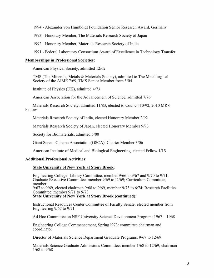
1994 - Alexander von Humboldt Foundation Senior Research Award, Germany
1993 - Honorary Member, The Materials Research Society of Japan
1992 - Honorary Member, Materials Research Society of India
1991 - Federal Laboratory Consortium Award of Excellence in Technology Transfer Memberships in Professional Societies: American Physical Society, admitted 12/62
TMS (The Minerals, Metals & Materials Society), admitted to The Metallurgical Society of the AIME 7/69, TMS Senior Member from 5/04
Institute of Physics (UK), admitted 4/73 American Association for the Advancement of Science, admitted 7/76 Materials Research Society, admitted 11/83, elected to Council 10/92, 2010 MRS Fellow Materials Research Society of India, elected Honorary Member 2/92 Materials Research Society of Japan, elected Honorary Member 9/93 Society for Biomaterials, admitted 5/00 Giant Screen Cinema Association (GSCA), Charter Member 3/06 American Institute of Medical and Biological Engineering, elected Fellow 1/15 Additional Professional Activities: State University of New York at Stony Brook:
Engineering College: Library Committee, member 9/66 to 9/67 and 9/70 to 9/71; Graduate Executive Committee, member 9/69 to l2/69; Curriculum Committee, member 9/67 to 9/69, elected chairman 9/68 to 9/69, member 9/73 to 6/74; Research Facilities Committee, member 9/71 to 9/73 State University of New York at Stony Brook (continued): Instructional Resources Center Committee of Faculty Senate: elected member from Engineering 9/67 to 9/71
Ad Hoc Committee on NSF University Science Development Program: 1967 – 1968
Engineering College Commencement, Spring l973: committee chairman and coordinator
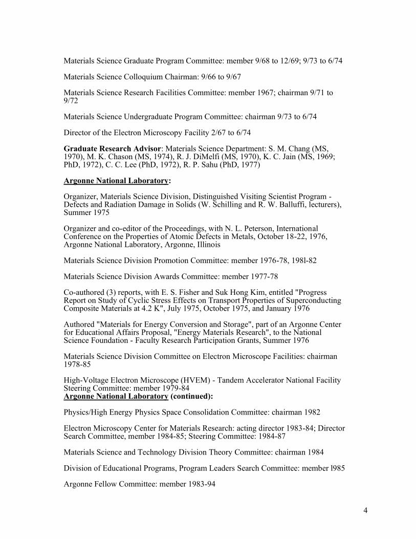
Director of Materials Science Department Graduate Programs: 9/67 to 12/69
Materials Science Graduate Admissions Committee: member 1/68 to 12/69; chairman 1/68 to 9/68
4
Materials Science Graduate Program Committee: member 9/68 to 12/69; 9/73 to 6/74
Materials Science Colloquium Chairman: 9/66 to 9/67
Materials Science Research Facilities Committee: member 1967; chairman 9/71 to 9/72
Materials Science Undergraduate Program Committee: chairman 9/73 to 6/74
Director of the Electron Microscopy Facility 2/67 to 6/74
Graduate Research Advisor: Materials Science Department: S. M. Chang (MS, 1970), M. K. Chason (MS, 1974), R. J. DiMelfi (MS, 1970), K. C. Jain (MS, 1969; PhD, 1972), C. C. Lee (PhD, 1972), R. P. Sahu (PhD, 1977)
Argonne National Laboratory:
Organizer, Materials Science Division, Distinguished Visiting Scientist Program - Defects and Radiation Damage in Solids (W. Schilling and R. W. Balluffi, lecturers), Summer 1975
Organizer and co-editor of the Proceedings, with N. L. Peterson, International Conference on the Properties of Atomic Defects in Metals, October 18-22, 1976, Argonne National Laboratory, Argonne, Illinois
Materials Science Division Promotion Committee: member 1976-78, 198l-82
Materials Science Division Awards Committee: member 1977-78
Co-authored (3) reports, with E. S. Fisher and Suk Hong Kim, entitled "Progress Report on Study of Cyclic Stress Effects on Transport Properties of Superconducting Composite Materials at 4.2 K", July 1975, October 1975, and January 1976
Authored "Materials for Energy Conversion and Storage", part of an Argonne Center for Educational Affairs Proposal, "Energy Materials Research", to the National Science Foundation - Faculty Research Participation Grants, Summer 1976
Materials Science Division Committee on Electron Microscope Facilities: chairman 1978-85 High-Voltage Electron Microscope (HVEM) - Tandem Accelerator National Facility Steering Committee: member 1979-84 Argonne National Laboratory (continued): Physics/High Energy Physics Space Consolidation Committee: chairman 1982 Electron Microscopy Center for Materials Research: acting director 1983-84; Director Search Committee, member 1984-85; Steering Committee: 1984-87
Materials Science and Technology Division Theory Committee: chairman 1984
Division of Educational Programs, Program Leaders Search Committee: member l985
Argonne Fellow Committee: member 1983-94
5
Rensselaer Polytechnic Institute:
Graduate Research Advisor: Lisa K. Koivisto (MEng 1998, Materials Science and Engineering); Paula J. Crawford (MEng 1999, Materials Science and Engineering); Chek B. Ng (MS 1998, Materials Science and Engineering; co-advisor L. S. Schadler); Thomas J. Webster (PhD Biomedical Engineering 2000; co-advisor R. Bizios); Petra Winberg (MS 2001, Polymer Science and Engineering, Lund Institute of Technology; co-advisors L. S. Schadler and J. I. Hong); John M. Nugent (PhD 2002, Materials Science and Engineering; co-advisor P. M. Ajayan); Ben J. Ash (PhD 2003, Materials Science and Engineering; co-advisor L. S. Schadler); Dongling Ma (PhD 2004, Materials Science and Engineering; co-advisor L. S. Schadler); Praveen Bhimaraj (PhD 2004, Materials Science and Engineering; co-advisor L. S. Schadler); Junrong Zheng (MS 2003, Chemistry); Aaron J. Dulgar (PhD 2005, Materials Science and Engineering; co-advisor R. Bizios); Jake D. Ballard (PhD 2005, Materials Science and Engineering; co-advisor R. Bizios); Tong Liu (PhD 2005, Materials Science and Engineering; co-advisor R. Ozisik); Paul Nicotera (MEng 2005, Materials Science and Engineering); Ludovico Dell’Acqua-Bellavitis (MS 2003, Materials Science and Engineering; MBA 2004, Lally School of Management and Technology; PhD 2007, Engineering Science); Frank W. Mont (MS 2006, Electrical, Computer and Systems Engineering; co-advisor E. F. Schubert); Ryan T. Schneider (MS 2008, Materials Science and Engineering; co-advisor R. Ozisik); Won Seok Lee (MS 2007, Materials Science and Engineering; co-advisor E. F. Schubert); Garima Vyas (MS 2007, Electrical, Computer and Systems Engineering; co-advisor E. F. Schubert); Joseph H. Nuffer (PhD 2011, Chemical and Biological Engineering; co-advisor J. S. Dordick); David J. Poxson (PhD 2011, Multidisciplinary Science; co-advisor E. F. Schubert); Jennifer E. Gagner (PhD 2012, Materials Science and Engineering; co-advisor J. S. Dordick); Peng Tao (PhD 2012, Materials Science and Engineering; co-advisor L. S. Schadler); Todd B. Abrams (MEng 2012, Materials Science and Engineering); Ying Li (PhD 2014, Materials Science and Engineering; co-advisor L. S. Schadler); Xi Qian (PhD 2014, Materials Science and Engineering; co-advisor J. S. Dordick); Nika Ogievetsky (MEng 2015, Materials Science and Engineering; co-advisor J. S. Dordick); Emily Elizabeth (Patrick J.) Downs (PhD 2017, Materials Science and Engineering; co-advisors L. S. Schadler and J. S. Dordick)
Vice President for Institute Relations Search Committee: member 1995-96
Chemical Engineering Department: Assistant Professor Search Committee, 1996-97; Department Head Search Committee, chairman 1997
Rensselaer Annual Fund: Faculty/Staff co-chair 1997-98 Provost Search Committee: member 1998-99 Rensselaer Polytechnic Institute (continued):
Internal Strategic Planning Committee for Biotechnology: member 2000; Biotechnology and Interdisciplinary Studies Building Advisory / Planning Committee: member 2000-03
Biotechnology Constellation Chair Search Committee: member 2000 – 2005
Faculty Compensation Advisory Committee: member 2002 – 2003 Vice President for Research Search Committee: member 2004 – 2005
6
Intellectual Property Policy Task Force: member 2005 – 2006 Provost Core Recruitment Committee: member 2006 – 2007
PhD Thesis Committees: Kevin E. Mello (PhD 1998, Materials Science and Engineering, S. Murarka, advisor); Jeffrey C. LaCombe (PhD 1999, Materials Science and Engineering, M. E. Glicksman, advisor); Sekyung Chang (PhD 2000, Materials Science and Engineering, R. H. Doremus, advisor); Jinseo Ahn (PhD 2003, Chemistry, J. V. Crivello, advisor); Yung Joon Jung (PhD 2003, Materials Science and Engineering, P. M. Ajayan, advisor); Ru Chen (PhD 2003, Chemistry, B. C. Benicewicz, advisor); Kumin (Charles) Yang (PhD 2006, Materials Science and Engineering, R. Ozisik, advisor); Amit Pratap Singh (PhD 2007, Materials Science and Engineering, G. Ramanath, advisor); Xuesong Li (PhD 2007, Materials Science and Engineering, P. M. Ajayan, advisor); Justin B. Bult (PhD 2007, Materials Science and Engineering, L. S. Schadler and P. M. Ajayan, advisors); Su Zhao (PhD 2007, Materials Science and Engineering, L. S. Schadler, advisor); Youngsuk Son (PhD 2008, Mechanical, Aerospace and Nuclear Engineering, T. Borca-Tasciuc, advisor); Binay K. Singh (PhD 2009, Chemical and Biological Engineering, G. Ramanath, advisor); Douglas Dukes (PhD 2010, Materials Science and Engineering, L. S. Schadler, advisor); Limeng Chen (PhD 2010, Materials Science and Engineering, L. S. Schadler and R. Ozisik, advisors); Lung-Ching Sang (PhD 2010, Chemical and Biological Engineering, M.-O. Coppens advisor); Frank W. Mont (PhD 2011, Electrical, Computer and Systems Engineering, E. F. Schubert, advisor); Won Seok Lee (PhD 2011, Engineering Science, E. F. Schubert, advisor); Rutvik Mehta (PhD 2011, Materials Science and Engineering, G. Ramanath, advisor); Yanliang Zhang (PhD 2011, Mechanical, Aerospace and Nuclear Engineering, T. Borca-Tasciuc, advisor); Jianing Gao (PhD 2012, Materials Science and Engineering, L. S. Schadler, advisor); Zepu Wang (PhD 2012, Materials Science and Engineering, L. S. Schadler, advisor); Yanping Chen (PhD 2013, Materials Science and Engineering, Y. Shi, advisor); Ming Ma (PhD 2013, Materials Science and Engineering, E. F. Schubert, advisor); Shantanu V. Sule (PhD 2013, Chemical and Biological Engineering, P. M. Tessier, advisor); Jiemin Wu (PhD 2016, Chemical and Biological Engineering, P. M. Tessier, advisor)
Founding Director, Rensselaer Nanotechnology Center 2001 – 2015 and NSF Nanoscale Science and Engineering Center for Directed Assembly of Nanostructures 2001 – 2013 Executive Producer, with L. S. Schadler and S. Garde, Molecularium® Project’s award-winning educational media: digital-dome show Molecularium: Riding Snowflakes, 2002-2005; giant-screen (2-D and 3-D) movie and high-definition video show Molecules to the MAX!, 2006-2009; interactive Website NanoSpace®, 2010-2012; Molecules to the MAX! DVD and Blu-Ray, 2014-2015; and the game app My Molecularium, 2016-2017
School of Engineering Outstanding Team Award, with S. Garde and L. S. Schadler, 2007; School of Engineering Outstanding Professor Award 2013 Other:
Short Courses: "Diffusion - Fundamentals and Applications", sponsored by the American Society for Metals, Academy for Metals and Materials, with L. L. Seigle, May 1-3, 1968, Boston, Massachusetts and February 3-5, 1969, Chicago, Illinois
7
Consultant, Materials Science Division, Argonne National Laboratory, Argonne, Illinois, May – June 1974
ERDA (Materials Sciences Program of Division of Physical Research) Workshop on Defects, Diffusion and Radiation Effects, participant and Chairman - Geothermal Study Group, at Oak Ridge National Laboratory, Oak Ridge, Tennessee, April 1977
Session Chairman, Defects in Metals, at the March Meeting of the American Physical Society, Chicago, Illinois, March 1979
Session Chairman, Defects, at the Fifth International Conference on Positron Annihilation, Lake Yamanaka, Japan, April 1979
Organizer, with N. L. Peterson, and Session Chairman, Symposium on Diffusion in Refractory Materials, Fall Meeting of The Metallurgical Society of AIME and the American Society of Metals, Milwaukee, Wisconsin, September 1979
Invited participant and speaker, Workshop on Techniques for Radiation Damage Analysis, sponsored by the Damage Analysis and Fundamental Studies Committee of the DOE Office of Fusion Energy, Oak Brook, Illinois, March 1979 Member, 1980 Selection Jury for The University of Chicago Awards for Distinguished Performance at Argonne National Laboratory
Participant, Department of Energy, Basic Energy Sciences Program Assessment, Germantown, Maryland, October 1981 Session Chairman, Advances in Techniques, Yamada Conference V on Point Defects and Defect Interactions in Metals, Kyoto, Japan, November 1981
Session Chairman, 2-D Angular Correlation, Second National Symposium on Positron Annihilation, Madras, India, February 1982 Session Chairman, Defects and Diffusion in Metals, March Meeting of the American Physical Society, Los Angeles, California, March 1983
Session Chairman, Point Defects and Clusters, Symposium on Advanced Photon and Particle Techniques for the Characterization of Defects in Solids, Materials Research Society Fall Meeting, Boston, Massachusetts, November 1984
Session Chairman, Seventh International Conference on Positron Annihilation, New Delhi, India, January 1985 Session Chairman, International Conference on Vacancies and Interstitials in Metals and Alloys, Berlin, Germany, September l986 Organizer and Chairman, with B. M. Klein, International Workshop on Electronic Structure of Defects in Metals and Alloys, Argonne National Laboratory, Argonne, Illinois, June l986 Other (continued): International Advisory Committee, International School on Electronic Band Structure and its Applications, Kanpur, India, October-November l986
8
Organizer and Chairman, with R. Sinclair and J. R. Weertman, Symposium on Characterization of Defects in Materials, at the Materials Research Society Meeting, Boston, Massachusetts, December l986
Session Chairman, Defects in Metals, TMS Annual Meeting, Denver, Colorado, February 1987
Organizer and Chairman, with F. E. Fujita, U.S.-Japan Seminar on Electronic Structure and Lattice Defects in Alloys, East-West Center, Honolulu, Hawaii, May 1987
Organizer and Chairman, with L. E. Brus, Department of Energy Council on Materials Science Panel on Research Opportunities on Clusters and Cluster-Assembled Materials, Monterey, California, January 1988 Session Chairman, Symposium on Powder Preparation at the Materials Research Society International Meeting on Advanced Materials, Ikebukuro, Tokyo, Japan, June 1988 Session Chairman, Physical Metallurgy Gordon Conference, New Hampshire, July 1988
Scientific Advisory Committee, International Conference on Diffusion in Metals and Alloys (DIMETA-88), Balatonfüred, Hungary, September 1988 Organizer and Chairman, with B. H. Kear, L. E. McCandlish, and D. E. Polk, Symposium on Multicomponent Ultrafine Microstructures, at the Materials Research Society Meeting, Boston, Mass., November-December 1988
Organizer and Meeting Chairman, with R. F. C. Farrow and A. M. Stacy, Materials Research Society 1989 Spring Meeting, San Diego, California, April 1989 Organizer and Session Chairman, Special Session on 'Cold Fusion' at the Materials Research Society 1989 Spring Meeting, San Diego, California, April 1989 Review Committee, chairman: Department of Mechanics and Materials Science, Rutgers University, May 1989 Advisory Committee, International Symposium on Physics of New Materials, Osaka, Japan, June 1989 Guest Physicist, National Synchrotron Light Source, Brookhaven National Laboratory, Upton, New York, 1986 - 1994 National Materials Advisory Board Committee on Materials with Submicron-Sized Microstructures: member 1986 - 1989 Organizer and Chairman, with D. Gupta and H. Jain, Symposium on Atomic Defects and Migration in Materials, at TMS-ASM Fall Meeting, Indianapolis, Indiana, October 1989 Review panel member, National Science Foundation, Division of Materials Research, Science & Technology Center (STC) proposals, December 1989; STC site visiting committee, April 1990 Other (continued):
9
Organizer and Chairman, with B. H. Kear, Acta Metallurgica Conference on Materials with Ultrafine Microstructures, Atlantic City, New Jersey, October 1990 Organizer and Chairman, Symposium on Multifunctional Nanophase Composites, at the 43rd Pacific Coast Regional Meeting of the American Ceramic Society, Seattle, Washington, October 1990 Session Chairman, Structure of Nanophase Materials, Symposium on Clusters and Cluster-Assembled Materials, Materials Research Society 1990 Fall Meeting, Boston, Massachusetts, November 1990 Session Chairman, Nanophase Materials, International Conference on Diffusion and Defects in Solids, Moscow to Perm, USSR, July 1991
Review panel member, National Science Foundation, Directorate of Engineering, Emerging Technologies Initiation Program proposals on Ultrafine Particle Engineering, July 1991 International Committee, First International Conference on Nanostructured Materials, Cancun, Mexico, September 1992 Recipient of Federal Laboratory Consortium 1991 Award for Excellence in Technology Transfer
Organizing Committee, First NIST Workshop on Nanostructured Materials, National Institute of Standards and Technology, Gaithersburg, Maryland, May 1992 Panel member, National Workshop on Critical Technologies Research: Opportunities for DOE, Advanced Materials Session, Lawrence Berkeley Laboratory, Berkeley, California, May 1992
Session Chairman, Ultrafine Ceramic Powders, Symposium on Nanophase Materials,
European Materials Research Society 1992 Fall Meeting, Strasbourg, France, November 1992 Session Chairman, Nanocomposites: Thin Films and Multilayers, Symposium on Nanophase and Nanocomposite Materials, Materials Research Society 1992 Fall Meeting, Boston, Massachusetts, December 1992 Novel Nanoscale Materials Working Group Leader and Organizer, Department of Energy Workshop on Innovation in Materials Processing and Manufacture: Exploratory Concepts for Energy Applications, Oak Ridge, Tennessee, March 1993 Co-Director, with G. C. Hadjipanayis, NATO Advanced Study Institute on Nanophase Materials: Synthesis-Properties-Applications, Corfu, Greece, June-July 1993 Session Chairman, Symposium on Forming, Characteristics and Processing of Ceramics, 24th Annual Meeting of the Fine Particle Society, Chicago, Illinois, August 1993 Session Chairman, Symposium on Frontiers of Materials Science and Engineering, 3rd IUMRS International Conference on Advanced Materials, Tokyo, Japan, September 1993
10
Other (continued): Symposium Chair and co-organizer with K. Niihara, K. Murata, and I. A. Aksay, Symposium on Nanophase and Nanocomposite Materials, The 3rd International Union of Materials Research Societies (IUMRS) International Conference on Advanced Materials, Tokyo, Japan, August-September 1993 Organizer and Chairman, with D. N. Seidman and P. D. Bristowe, Symposium on Atomic Scale Imperfections in Materials: R. W. Balluffi Fest, at the Materials Research Society 1993 Fall Meeting, Boston, Mass., November-December 1993 Chairman and co-organizer with H. Gleiter and J.-Ph. Ansermet, Engineering Foundation Conference on Nanophase Materials, Davos, Switzerland, March 1994
Organizer and Chairman, with P. Jena, Division of Materials Physics Focussed Sessions on Clusters and Cluster-Assembled Materials, at the American Physical Society Meeting, Pittsburgh, Pennsylvania, March 1994
Organizing Committee and Session Chairman, International Conference on the Structure and Properties of Brittle and Quasiplastic Materials (SPM'94), Riga, Latvia, June 1994 The Washington Technology Center, Advanced Materials Technology Center Advisory Committee, member 1991 - 1992; Advanced Materials & Manufacturing Group Advisory Committee, member 1993 - 1994 International Advisory Committee, Forum on New Materials, 8th CIMTEC (Inter-national Context on Modern Materials Technologies), Florence, Italy, June-July 1994
Advisory Committee, Second International Conference on Nanostructured Materials, Stuttgart, Germany, October 1994
Session Chairman, Grain Size and Thermomechanical Properties, Symposium on Grain Size and Mechanical Properties-Fundamentals and Applications, Materials Research Society 1994 Fall Meeting, Boston, Massachusetts, November-December 1994
International Advisory Committee, International Workshop on Clusters and Nanostructured Materials, Puri, Orissa, India, December 1994-January 1995 International Advisory Board, International Symposium on the Science and Technology of Atomically Engineered Materials, Richmond, Virginia, October-November 1995 Organizer, with J. E. E. Baglin, and Moderator, Forum on Electronic Publishing Initiatives, at the Materials Research Society 1995 Spring Meeting, San Francisco, California, April 1995 Session Chairman, Symposium on Processing and Properties of Nanocrystalline Materials, TMS-ASM Materials Week, Cleveland, Ohio, October 1995 Board of Advisors, Gorham Advanced Materials Institute Conference on Nanostructured Materials and Coatings, Atlanta, Georgia, November 1995
11
International Advisory Committee, International Symposium on Metastable Mechanically Alloyed and Nanocrystalline Materials (ISMANAM-96), Rome, Italy, May 1996 Other (continued): Steering Committee, Advisory Committee, and Session Chairman, Third International Conference on Nanostructured Materials, Kona, Hawaii, July 1996 International Advisory Committee, Eighth International Symposium on Physics of Materials: Materials Science and Physics of Low Dimensional Structures and Cluster Assembly, Hangzhou, China, October 1996 International Advisory Committee/Scientific Committee, International Conference on the Physics of Disordered Materials, University of Rajasthan, Jaipur, India, January 1997 International Program Committee, Second International Conference on MicroMaterials (Micro Mat '97), Berlin, Germany, April 1997 Member, Boards of Examiners: Department of Nuclear Physics, University of Madras, India, Ph.D. Theses of V. Manohar (1984), S. Sankar (1987), S. R. Dhanalakshmi (1988), A. Bharathi (1989-1990); Departement de Physique des Matériaux, Université Claude Bernard-Lyon I, France, Ph.D. Thesis of V. Paillard (1993); Department of Physics, Jadavpur University, Calcutta, India, Ph.D. Thesis of S. Roy (1993); Department of Physics, State University of New York at Albany, Ph.D. Thesis of G. Gopalakrishnan (1998), Department of Materials Science and Engineering, Northwestern University, Ph.D. Theses of J. D. Hansen (1991) and D. N. Dunn (1992); Departement de Science de l’Energie et des Matériaux, INRS-ÉMT, Université du Québec, Ph.D. Thesis of F. Variola (2010) Graduate Research Advisor: Department of Materials Science and Engineering, Northwestern University, M.S. Thesis (1989) and Ph.D. Theses (1991) of G. W. Nieman (co-advisor with J. R. Weertman), Ph.D. Thesis (1995) of G. E. Fougere (co-advisor with J. R. Weertman), Ph.D. Thesis (1996) of P. G. Sanders (co-advisor with J. R. Weertman) International Advisory Committee, International Symposium on Metastable, Mechanically Alloyed and Nanocrystalline Materials (ISMANAM-97), Sitges (Barcelona), Spain, September 1997 Expert Selection Committee for Nanostructure Physics Professor in the Physics Department, School of Engineering Physics, Royal Institute of Technology, Stockholm, Sweden: member 1996-97
Visiting Committee for Natural Sciences and Engineering Research Council of Canada Industrial Research Chair in Microengineered Materials at the University of Toronto, Toronto, Canada, November 1996
Editorial Board, Bulletin of Materials Science, Indian Academy of Sciences, Bangalore, 1992-1996 Atomic Transport Committee of the Materials Science Division of the American Society of Metals: member 1987 - 2000
12
Materials Research Society: Program Committee, member 1987-90; Spring Meeting Chair 1989; Council, elected member 1993-95; Audit Committee, member 1993-95, chairman 1994-95; Grass Roots Education Committee, member 1992-94; Long Range Planning Committee, chairman 1996-97; Public Affairs Committee, member 1994-2000; Fellow 2010 Other (continued): Reference Group member (advisor), Swedish Materials Research Consortium on Clusters and Ultrafine Particles, 1991-98 International Committee on Nanostructured Materials: chairman 1992-1996; member 1992-2000 University Materials Council: member 1995-2000 Associate Editorial Board, Materials Letters, North-Holland Publishing Co., Amsterdam, 1981-2006 Founding Principal Editor, Nanostructured Materials, Acta Metallurgica, Inc., Pergamon Press, Elsevier Science Ltd., Oxford, 1991-99
Board of Advisors, Encyclopedia of Materials Science and Engineering for the Third Millenium, Pergamon Press, Elsevier Science Ltd., 1994-98 International Advisory Committee and Program Committee, Fourth International Conference on Nanostructured Materials (NANO’98), Stockholm, Sweden, June 1998 Reviewer of proposals and publications for: Department of Energy, Department of the Army, National Science Foundation, Research Corporation, Academic Press, The Institute of Physics, Acta Metallurgica, Scripta Metallurgica, Canadian Journal of Physics, Journal of Applied Physics, Applied Physics Letters, Journal of Nuclear Materials, Physical Review, Physical Review Letters, Physica Status Solidi, Metallurgical Transactions, Gas Research Institute, Petroleum Research Fund (American Chemical Society), Materials Science and Engineering, Annales de Chimie: science des matèriaux, Materials Letters, Journal of Materials Research, International Journal of Physics and Chemistry of Solids, Nuclear Instruments and Methods in Physics Research, Surface Science, American Society for Metals, Materials Research Society, State of Connecticut-Department of Higher Education, Connecticut Innovations, Physics Letters, Australian Research Council, Journal of Solid State Chemistry, The Washington Technology Center, Chemistry of Materials, Nature, Kluwer Academic Publishers, Pergamon Press, Elsevier Science Publishers, CRC Press, Chapman & Hall, John Wiley & Sons, National Research Council, National Institute of Standards and Technology, Journal of Aerosol Science, North Atlantic Treaty Organization, Science, International Science Foundation, The Journal of Physical Chemistry, Aerosol Science and Technology, The Journal of Vacuum Science and Technology, Swedish Research Council for Engineering Sciences (TFR), Hong Kong Research Grants Council, Philosophical Magazine and Philosophical Magazine Letters, Materials Chemistry and Physics, Consiglio Nazionale delle Ricerche (Italy), City University of Hong Kong, Journal of the American Chemical Society, Advanced Materials, Europhysics Letters, W. M. Keck Foundation, Michigan Life Sciences Corridor (Washington Advisory Group), Louisiana Board of Regents, Laura Bassi Centres of Expertise (Austria), Science Foundation Ireland, etc.
13
Panel Chairman, World Technology Evaluation Center (WTEC) Global Assessment of Research and Development Status and Trends in Nanoparticles, Nanostructured
Materials, and Nanodevices (Nanostructure Science and Technology), sponsored by the NSF, AFOSR, ONR, DOC, NIST, DOE, NIH, and NASA, 1996-98
Alexander von Humboldt Foundation Senior Research Award 1994 (Max-Planck-Institut für Mikrostrukturphysik, Halle, Germany 1995-98) Other (continued): Judge, The 1998 Discover Magazine Awards for Technological Innovation: Emerging Technology, February 1998 Review Committee: Department of Ceramic and Materials Engineering, Rutgers University, April 1998 Discussion Leader, Gordon Research Conference on High Temperature Materials Processing and Diagnostics, Plymouth, New Hampshire, July 1998 International Advisory Committee, International Symposium on Metastable, Mechanically Alloyed and Nanocrystalline Materials (ISMANAM-98), Wollongong, Australia, December 1998 Advisory Board, 1999 Discover Magazine Awards
Moderator, Applications: Consolidated Nanostructures Session, at the OSTP Committee on Technology Interagency Working Group on NanoScience, Engineering and Technology Workshop on Vision for Nanotechnology R&D in the Next Decade, National Science Foundation, Arlington, Virginia, January 1999 Chairman, with P. M. Ajayan, Engineering Foundation Conference on Nanocomposite Materials: Design and Applications, Girdwood (Anchorage), Alaska, March-April 1999 International Advisory Board, International Symposium on Clusters and Nanostructures, Richmond, Virginia, October 1999 Program Committee, 3rd International Conference and Exhibition on MicroMaterials (MicroMat 2000), Berlin, Germany, April 2000 International Advisory Committee and Session Charman, Fifth International Conference on Nanostructured Materials (NANO’2000), Sendai, Japan, August 2000 Section Editor: Characterization Techniques, with E. A. Stern, Current Opinion in Solid State & Materials Science, A. K. Cheetham, M. S. Dresselhaus, and Sir J. M. Thomas (Eds.), Volume 4, Issue 4, 1999 (Current Chemistry Ltd., Letchworth) International Advisory Committee, International Symposium on Metastable, Mechanically Alloyed and Nanocrystalline Materials (ISMANAM-99) and Euro Conference on Gas Phase Synthesis of Nanocrystalline Materials, Dresden, Germany, August-September 1999 International Advisory Committee, International Conference on Mass and Charge Transport in Inorganic Materials - Fundamentals to Devices, Venice (Jesolo Beach), Italy, May-June 2000
14
Panel Member, Vision 2020-Materials Technology Roadmap Workshop II, Golden, Colorado, September-October 1999 Advisory Board, Institute for Nanotechnology and (since 2002) Nanotechnology Program, Forschungszentrum Karlsruhe (in conjunction with the Universities of Karlsruhe and Strasbourg), 1999-2004 Other (continued): Scientific Advisory Board, Journal of Metastable and Nanostructured Materials, Trans Tech Publications, 2000-present International Advisory Committee, International Symposium on Metastable, Mechanically Alloyed and Nanocrystalline Materials (ISMANAM 2000), St. Catherine’s College, Oxford, England, July 2000 Editorial Board, Journal of Nanoscience and Nanotechnology, American Scientific Publishers, 2001-present Editorial Advisory Board, Encyclopedia of Nanoscience and Nanotechnology, American Scientific Publishers, 2002 International Scientific Committee, 7th Annual Conference on Ceramics, Cells and Tissues: Biomimetic Engineering, New Role for Ceramics, Faenza, Italy, June 2001
International Advisory Committee, International Symposium on Metastable, Mechanically Alloyed and Nanocrystalline Materials (ISMANAM 2001), University of Michigan, Ann Arbor, Michigan, June 2001 Organizing Committee, United Engineering Foundation Conference on Novel Synthesis and Processing of Nanostructured Coatings for Protection Against Degradation, Davos, Switzerland, August 2001 Session Chairman and Faculty Lecturer, Nanobiotechnology, Second Annual Conference on Regenerative Medicine, Washington, D.C., December 2001 Program Committee, BioMEMS and Smart Nanostructures, SPIE International Symposium on Micro/MEMS, Adelaide, Australia, December 2001 Scientific Program Committee, Sixth International Conference on Nanostructured Materials (Nano 2002), Orlando, Florida, June 2002 RIKEN (The Institute of Physical and Chemical Research) Eminent Scientist Award, Japan, December 2001
International Advisory Committee of ICMAT 2003 (International Conference on Materials for Advanced Technologies), Singapore, June-July 2003 Director and lecturer, NSF Chautauqua Short Course on Nanotechnology and Nanostructured Materials and Devices, Rensselaer Polytechnic Institute, June 2002 2002 Motorola Research Visionary Board
15
Global Trends 2015: Science and Technology – Biotechnology, Nanotechnology, Advanced Materials, and Information Technology Roundtable hosted by the Central Intelligence Agency Directorate of Science and Technology and the Library of Congress Federal Research Division, Washington, D. C., July 2002 Organizer (with Joanna R. Groza, Dan Descalu, and Maria Zaharescu) and lecturer, NSF Workshop on Communication and Integration in Nanomaterials, Transylvania University, Brasov, Romania, September-October 2002 Other (continued): Advisory Board, International Conference on Nano-Micro-Interfaces (NAMIX), Berlin, Germany, May 2003 International Scientific Committee, 8th Annual Conference on Ceramics, Cells and Tissues: Bioceramic Surfaces (behavior in vitro and in vivo), Faenza, Italy, March 2003 Program Committee, Naniotechnology Conference at the SPIE First International Symposium on Microtechnologies for the New Millennium, Maspalomas, Gran Canaria, Canary Islands, Spain, May 2003
Steering Committee Member and Workshop Participant, NSF-NNI Nanomaterials Grand Challenges Workshop, Arlington, Virginia, June 2003 International Advisory Committee, 10th International Symposium on Metastable, Mechanically Alloyed and Nanocrystalline Materials (ISMANAM 2003), Foz do Iguaçu, Brazil, August 2003
International Advisory Board, International Symposium on Clusters and Nanoassemblies: Physical and Biological Systems, Richmond, Virginia, November 2003 International Program Committee, 4th International Conference on Micromaterials and Nanomaterials (MicroMat 2004), Berlin, Germany, April 2004 Director and lecturer, NSF Chautauqua Short Course on Nanotechnology and Nanostructured Materials and Devices, Rensselaer Polytechnic Institute, June 2003 Advisory Board, 7th International Conference on Nanostructured Materials (NANO 2004), Wiesbaden, Germany, June 2004 2003 Deutsche Bank Prize: Pioneer in Nanotechnology – Nanomaterials, Berlin, Germany, May 2003 Nanotechnology Technical Advisory Group (N-TAG) to the US President’s Council of Advisors on Science and Technology (PCAST), June 2003-09 Permanent International Scientific Committee, Annual Conference Series on Ceramics, Cells and Tissues (CCT), Italian National Research Council, Institute of Science and Technology for Ceramics, Faenza, Italy, 2003-12 Advisory Committee, Second Conference on Local and Nanoscale Structure in Complex Systems (LNSCS-II), Dynamic Energy Landscapes and Functional Systems, March 2004, Santa Fe, New Mexico.
16
Organizer, with Catherine Brechignac, U.S.-France Workshop on the Intersection between Biology, Chemistry, and Physics for Creating Materials with Nanoscale Architectures, Honfleur, France, May 2004 NNI-SRC Consultative Working Group on Novel Materials and Assembly Methods for Extending Charge-Based Technologies, 2004-07 Director and lecturer, NSF Chautauqua Short Course on Nanotechnology and Nanostructured Materials and Devices, Rensselaer Polytechnic Institute, June 2004 Other (continued): Perspective Committee for the Research Center Jülich, Germany commissioned by the German Federal Ministry of Education and Research (BMBF) and the Ministry of Science and Research of the State of North Rhine-Westphalia, 2004 Expert Selection Committee for the Professor in Nanotechnology in the Faculty of Science and Technology at Uppsala University, Uppsala, Sweden, 2004 Advisory Board, Synergistic Partnership for Research and Education on Functional and Nanostructured Materials, an NSF PREM at the University of Puerto Rico-Mayagüez and the University of Wisconsin-Madison, 2004-09
Advisory Committee, Conference on Design and Characterization of Advanced Materials (DCAM-2004), Banaras Hindu University, Varanasi, India, December 2004
International Advisory Board (Steering Committee), and Co-Chair of the Special Symposium "Disclosing Materials at the Nanoscale" of the 11th International Ceramics Congress, CIMTEC 2006 in Acireale, Sicily, Italy, June 2006 Peer Group for evaluation of the Technology-Oriented Program TOP NANO 21 (2000 - 2003) in Switzerland, commissioned by the Swiss Federation represented by the Commission for Technology and Innovation, 2004-05 Director and lecturer, NSF Chautauqua Short Course on Nanotechnology and Nanostructured Materials and Devices, Rensselaer Polytechnic Institute, June 2005 Perspective Committee for the Research Center Karlsruhe, Germany commissioned by the German Federal Ministry of Education and Research (BMBF) and the Ministry of Trade and Commerce of the State of Baden-Württemburg, 2005-06 Director and lecturer, NSF Chautauqua Short Course on Nanotechnology and Nanostructured Materials and Devices, Rensselaer Polytechnic Institute, June 2006 Scientific and Industrial Advisory Board, Education and Research Unit (ERU): Particles and Surface Engineering, Competence Centre for Material Science and Technology (CCMX), Switzerland, 2006-12 International Advisory Board, Chairman, National Nanotechnology Center of Thailand (NANOTEC), National Science and Technology Development Agency (NSTDA), Thailand, 2006-08
Scientific Review Panel, Virginia Bioinformatics Institute, Virginia Polytechnic Institute and State University, Blacksburg, Virginia, June 2007
17
International Advisory Board (to the German Science Council), Karlsruhe Institute of Technology (KIT), Karlsruhe, Germany, 2007-10 Advisory Board, Forest Bioproducts Research Initiative, The University of Maine, Orono, Maine, 2007-10 International Advisory Board, International Conference on Nano Science and Technology (ICONSAT-2008), Chennai, India, February 2008 Other (continued): Advisory Committee, NanoBiotech 2007, Rensselaer Polytechnic Institute, September 2007 Scientific Advisory Board, Virginia Bioinformatics Institute, Virginia Polytechnic Institute and State University, Blacksburg, Virginia, 2007-11 International Advisory Committee, 9th International Conference on Nanostructured Materials – NANO 2008 (NANO–RIO), Rio de Janeiro, Brazil, June 2008 International Advisory Board, First International Conference on Tissue Engineering and Stem Cell Research using Nanomaterials (NANOBIO 2009), Amrita Institute of Medical Sciences, Kochi, India, February 2009
Evaluation Panel Member, Spanish Research Council (CSIC – Consejo Superior de
Investigaciones Científicas) Materials Research Centers, Spain, 2008-09 Senior International Advisor, Global Green Research Institute, Handong Global
University, Pohang, South Korea, 2009-10 Participant, NSF-WTEC International Study of the Long-term Impacts and Future Opportunities for Nanoscale Science and Engineering, Chicago Workshop, March 2010 International Advisory Board, 2nd International Conference on Disclosing Materials at the Nanoscale, 12th International Ceramics Congress (CIMTEC 2010), Montecatini Terme, Tuscany, Italy, June 2010 International Advisory Board, X International Conference on Nanostructured Materials (NANO 2010), Rome, Italy, September 2010
Scientific and Industrial Advisory Board, International GENNESYS Congress on
Nanotechnology and Research Infrastructures, Barcelona, Spain, May 2010
Co-President, 13th Ceramics, Cells and Tissues (13 CCT) Seminar and Meeting, Regenerative Nanomedicine, Tissue and Genetic Engineering: the Role of Ceramics, Italian National Research Council, Institute of Science and Technology for Ceramics, Faenza, Italy, May 2011 Founding Member, Advisory Board, Forest Bioproducts Research Institute, The University of Maine, Orono, Maine, 2010-2016
18
Science Advisory Board, The 1st World Congress of Nanomedicine (Nanomedicine 2010) – Integrative Nanotechnology for Biomedicine, Beijing, China, October 2010
International Advisory Board and session chair, YUCOMAT Conferences of the MRS-
Serbia, 2010-present International Advisory Committee, International Workshop on Functional Materials
(IWFM), Berhampur, India, 2011 RUSNANOPRIZE 2013 nominee, finalist, and Expert Group member Visiting Professor, School of Materials Science and Engineering, Shanghai Jiao Tong
University, Shanghai, China, May 2014 Other (continued): Elected to the College of Fellows of the American Institute of Medical and Biological
Engineering, January 2015 International Scientific Committee and Session Chair, 1st Biennial Conference
BioMaH – Biomaterials for Healthcare, Biomaterials for Tissues and Genetic Engineering and the Role of Nanotechnology, Rome, Italy, October 2016
Seminar and Meeting on Tissue Regeneration: Advanced Ceramics and Composites (TRACE), Department of Surgical Sciences and Integrated Diagnostics, Università degli Studi di Genova, Genoa, Italy, October 2017
Elected to the Natioanal Academy of Inventors, December 2017
19
Grants, Contracts and Fellowships: State University of New York at Stony Brook Graduate School, Faculty Fellowship, Summer 1967 ($1,400) State University of New York at Stony Brook Graduate School, Grants-in-Aid (various), 1967-1970 ($4,429 total) State University of New York Research Foundation, Faculty Fellowship, Summer 1968 ($1,500) State University of New York Research Foundation, Grant-in-Aid, "Vacancy Precipitation in Quenched Gold", 5/1/67 - 5/1/69 ($500) State University of New York Research Foundation, Grant-in-Aid, "Effect of Impurities on the Migration of Vacancies in Gold", 1/1/68 - 1/1/70 ($200) National Science Foundation, Research Initiation Grant, "Vacancy-Impurity Interactions in Dilute Aluminum Alloys", 6/1/68 - 3/31/70 ($15,000) National Science Foundation, Research Grant, "Solute-Vacancy Interactions in Dilute Alloys", 11/1/70 - 4/31/73 ($58,400) National Science Foundation, Faculty Research Participation Grant, Argonne Center for Educational Affairs, "Materials Used in Energy Conversion Systems", Summer 1975 ($18,480) National Science Foundation, Grant, "International Conference on the Properties of Atomic Defects in Metals", Argonne National Laboratory, 1976 ($2,500) Atomic Energy Commission, Research Contracts - Argonne: Metal Physics and Effects of Cyclic Loading on Electrical Conduction, 7/74 - 6/75 ($967,000) Energy Research and Development Administration, Research Contracts - Argonne: Metal Physics, Diffusion Studies, and Effects of Cyclic Loading on Electrical Conduction, 7/75 - 9/76 ($1,393,900) Energy Research and Development Administration, Research Contracts - Argonne: Metal Physics and Diffusion Studies, 10/76 - 9/77 ($1,015,700) National Science Foundation, Supplementary Research Grant in collaboration with Prof. S. Berko, Brandeis University, "Positron Annihilation Spectroscopic Study of Vacancy Defects in Aluminum", 11/1/80 - 10/31/81 ($27,688) National Science Foundation, International Travel Grant, India 1/27/82 - 2/24/82 ($1,943) Department of Energy, Research Contract - Argonne: Metal Physics, 10/77 - 9/82 ($5,546,000) Department of Energy, Research Contract - Argonne: Electron Microscopy Center for Materials Research, 10/83 - 9/84 ($716,000) National Science Foundation, International Travel Grant, India 1/3/85 - 2/1/85 ($1,900)
20
Grants, Contracts and Fellowships (continued): Department of Energy, Research Contract - Argonne: Defects in Metals and Alloys, 10/82 - 9/86 ($4,362,000) Office of Naval Research, Workshop Support, International Workshop on "Electronic Theory of Defects in Metals and Alloys", 6/86 ($15,000) Argonne Universities Associates Trust Fund, Workshop Support, International Workshop on "Electronic Theory of Defects in Metals and Alloys", 6/86 ($7,500) National Science Foundation, International Travel Grant, India, 10/16/86 - 11/14/86 ($1,974) National Science Foundation, U.S.-Japan Seminar on "Electronic Structure and Lattice Defects in Alloys", 5/87 ($10,550) National Science Foundation, Office of Naval Research, and Air Force European Office of Aerospace Research and Development, Engineering Foundation Conference on "Nanophase Materials", 3/94 ($15,000) Department of Energy, Research Contract - Argonne: Nanocrystalline Materials, 10/86 - 3/95 (ca. $1,750,000) Rensselaer Polytechnic Institute, Strategic Initiatives Grant on “Nanostructured Materials”, 9/97-5/00 ($35,000) National Science Foundation, “Mechanical and Molecular Behavior of Nanoparticulate/Polymer Composites”, with L. S. Schadler et al., 8/98-7/01 ($562,717) Office of Naval Research, “Mechanical and Molecular Behavior of Nanoparticulate/Polymer Composites”, with L. S. Schadler et al., 1/99-9/01 ($100,000) National Science Foundation, “A PhD Co-op Program”, with L. S. Schadler and D. J. Duquette, 4/99-8/05 ($555,102) National Science Foundation, Army Research Office, Office of Naval Research, Nanophase Technologies Corporation, RHK Technology Inc., and JEOL USA Inc., United Engineering Foundation Conference on “Nanocomposite Materials: Design and Applications”, with P. M. Ajayan, 3-4/99 ($37,000) National Science Foundation, “Acquisition of State of the Art Micro-Raman Spectrometer”, with L. S. Schadler et al., 6/99-5/00 ($162,534) Eastman Kodak Company, “Partnership in Nanotechnology”, 9/99-8/04 ($660,000) Albany International Corporation, “Partnership in Nanotechnology”, 6/00-5/04 ($480,000) ABB Ltd., “Partnership in Nanotechnology”, 1/00-6/12 ($1,792,000) IBM Corporation, “Partnership in Nanotechnology”, 9/00-6/14 ($1,467,500) Philip Morris USA, “Partnership in Nanotechnology”, 1/01-12/06 ($2,300,000)
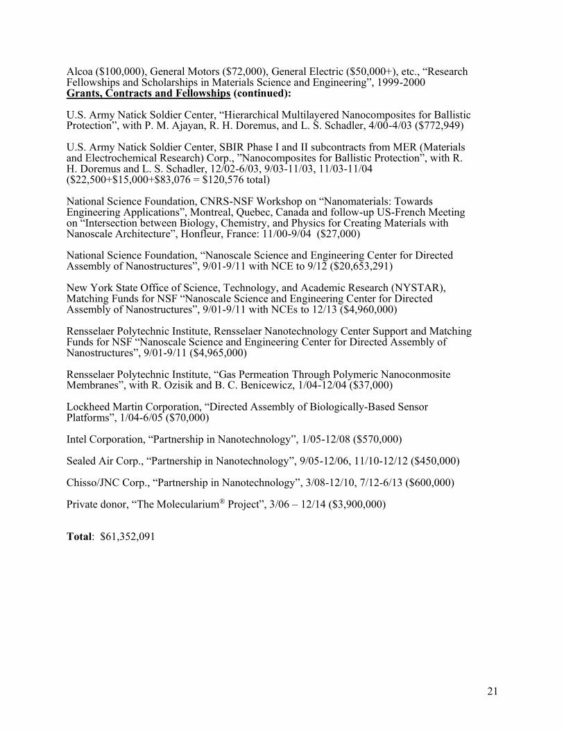
21
Alcoa ($100,000), General Motors ($72,000), General Electric ($50,000+), etc., “Research Fellowships and Scholarships in Materials Science and Engineering”, 1999-2000 Grants, Contracts and Fellowships (continued): U.S. Army Natick Soldier Center, “Hierarchical Multilayered Nanocomposites for Ballistic Protection”, with P. M. Ajayan, R. H. Doremus, and L. S. Schadler, 4/00-4/03 ($772,949) U.S. Army Natick Soldier Center, SBIR Phase I and II subcontracts from MER (Materials and Electrochemical Research) Corp., ”Nanocomposites for Ballistic Protection”, with R. H. Doremus and L. S. Schadler, 12/02-6/03, 9/03-11/03, 11/03-11/04 ($22,500+$15,000+$83,076 = $120,576 total) National Science Foundation, CNRS-NSF Workshop on “Nanomaterials: Towards Engineering Applications”, Montreal, Quebec, Canada and follow-up US-French Meeting on “Intersection between Biology, Chemistry, and Physics for Creating Materials with Nanoscale Architecture”, Honfleur, France: 11/00-9/04 ($27,000) National Science Foundation, “Nanoscale Science and Engineering Center for Directed Assembly of Nanostructures”, 9/01-9/11 with NCE to 9/12 ($20,653,291) New York State Office of Science, Technology, and Academic Research (NYSTAR), Matching Funds for NSF “Nanoscale Science and Engineering Center for Directed Assembly of Nanostructures”, 9/01-9/11 with NCEs to 12/13 ($4,960,000) Rensselaer Polytechnic Institute, Rensselaer Nanotechnology Center Support and Matching Funds for NSF “Nanoscale Science and Engineering Center for Directed Assembly of Nanostructures”, 9/01-9/11 ($4,965,000) Rensselaer Polytechnic Institute, “Gas Permeation Through Polymeric Nanoconmosite Membranes”, with R. Ozisik and B. C. Benicewicz, 1/04-12/04 ($37,000) Lockheed Martin Corporation, “Directed Assembly of Biologically-Based Sensor Platforms”, 1/04-6/05 ($70,000) Intel Corporation, “Partnership in Nanotechnology”, 1/05-12/08 ($570,000) Sealed Air Corp., “Partnership in Nanotechnology”, 9/05-12/06, 11/10-12/12 ($450,000) Chisso/JNC Corp., “Partnership in Nanotechnology”, 3/08-12/10, 7/12-6/13 ($600,000) Private donor, “The Molecularium® Project”, 3/06 – 12/14 ($3,900,000) Total: $61,352,091
22
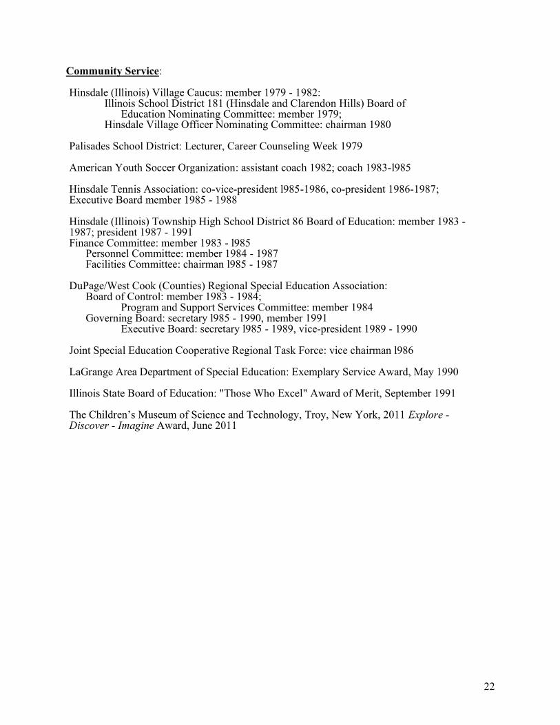
Community Service: Hinsdale (Illinois) Village Caucus: member 1979 - 1982:
Illinois School District 181 (Hinsdale and Clarendon Hills) Board of Education Nominating Committee: member 1979;
Hinsdale Village Officer Nominating Committee: chairman 1980 Palisades School District: Lecturer, Career Counseling Week 1979
American Youth Soccer Organization: assistant coach 1982; coach 1983-l985
Joint Special Education Cooperative Regional Task Force: vice chairman l986 LaGrange Area Department of Special Education: Exemplary Service Award, May 1990 Illinois State Board of Education: "Those Who Excel" Award of Merit, September 1991 The Children’s Museum of Science and Technology, Troy, New York, 2011 Explore - Discover - Imagine Award, June 2011
23
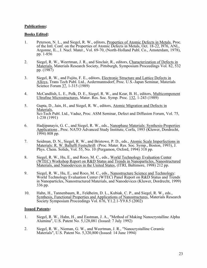
Publications: Books Edited: 1. Peterson, N. L., and Siegel, R. W., editors, Properties of Atomic Defects in Metals, Proc.
of the Intl. Conf. on the Properties of Atomic Defects in Metals, Oct. 18-22, l976, ANL, Argonne, IL., J. Nucl. Mater., Vol. 69-70, (North-Holland Publ. Co., Amsterdam, 1978), pp. 1-856
2. Siegel, R. W., Weertman, J. R., and Sinclair, R., editors, Characterization of Defects in
Materials, Materials Research Society, Pittsburgh, Symposium Proceedings Vol. 82, 532 pp. (1987)
3. Siegel, R. W., and Fujita, F. E., editors, Electronic Structure and Lattice Defects in
Alloys, Trans Tech Publ. Ltd., Aedermannsdorf, Proc. U.S.-Japan Seminar, Materials Science Forum 37, 1-315 (1989)
4. McCandlish, L. E., Polk, D. E., Siegel, R. W., and Kear, B. H., editors, Multicomponent
Ultrafine Microstructures, Mater. Res. Soc. Symp. Proc. 132, 1-243 (1989) 5. Gupta, D., Jain, H., and Siegel, R. W., editors, Atomic Migration and Defects in
Materials, Sci-Tech Publ. Ltd., Vaduz, Proc. ASM Seminar, Defect and Diffusion Forum, Vol. 75, 1-238 (1991)
6. Hadjipanayis, G. C., and Siegel, R. W., eds., Nanophase Materials: Synthesis-Properties
Applications , Proc. NATO Advanced Study Institute, Corfu, 1993 (Kluwer, Dordrecht, 1994) 808 pp.
7. Seidman, D. N., Siegel, R. W., and Bristowe, P. D., eds., Atomic Scale Imperfections in
Materials: R. W. Balluffi Festschrift (Proc. Mater. Res. Soc. Symp., Boston, 1993), J. Phys. Chem. Solids, Vol. 55, No. 10 (Pergamon, Oxford, 1994) 318 pp.
8. Siegel, R. W., Hu, E., and Roco, M. C., eds., World Technology Evaluation Center
(WTEC) Workshop Report on R&D Status and Trends in Nanoparticles, Nanostructured Materials, and Nanodevices in the United States, (ITRI, Baltimore, 1998) 212 pp.
9. Siegel, R. W., Hu, E., and Roco, M. C., eds., Nanostructure Science and Technology:
World Technology Evaluation Center (WTEC) Panel Report on R&D Status and Trends in Nanoparticles, Nanostructured Materials, and Nanodevices (Kluwer, Dordrecht, 1999) 336 pp.
10. Hahn, H., Tannenbaum, R., Feldheim, D. L., Kubiak, C. P., and Siegel, R. W., eds.,
Synthesis, Functional Properties and Applications of Nanostructures, Materials Research Society Symposium Proceedings Vol. 676, Y1.2.1-Y9.8.5 (2002)
Issued Patents: 1. Siegel, R. W., Hahn, H., and Eastman, J. A., "Method of Making Nanocrystalline Alpha
Alumina", U.S. Patent No. 5,128,081 (Issued: 7 July 1992) 2. Siegel, R. W., Nieman, G. W., and Weertman, J. R., "Nanocrystalline Ceramic
Materials", U.S. Patent No. 5,320,800 (Issued: 14 June 1994)
24
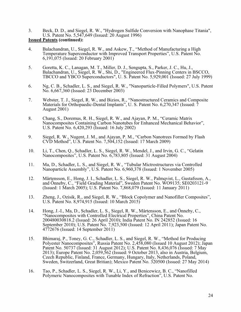
3. Beck, D. D., and Siegel, R. W., "Hydrogen Sulfide Conversion with Nanophase Titania", U.S. Patent No. 5,547,649 (Issued: 20 August 1996)
Issued Patents (continued): 4. Balachandran, U., Siegel, R. W., and Askew, T., “Method of Manufacturing a High
Temperature Superconductor with Improved Transport Properties”, U.S. Patent No. 6,191,075 (Issued: 20 February 2001)
5. Goretta, K. C., Lanagan, M. T., Miller, D. J., Sengupta, S., Parker, J. C., Hu, J.,
Balachandran, U., Siegel, R. W., Shi, D., "Engineered Flux-Pinning Centers in BSCCO, TBCCO and YBCO Superconductors", U. S. Patent No. 5,929,001 (Issued: 27 July 1999)
6. Ng, C. B., Schadler, L. S., and Siegel, R. W., "Nanoparticle-Filled Polymers", U.S. Patent
No. 6,667,360 (Issued: 23 December 2003) 7. Webster, T. J., Siegel, R. W., and Bizios, R., “Nanostructured Ceramics and Composite
Materials for Orthopaedic-Dental Implants”, U. S. Patent No. 6,270,347 (Issued: 7 August 2001)
8. Chang, S., Doremus, R. H., Siegel, R. W., and Ajayan, P. M., “Ceramic Matrix
Nanocomposites Containing Carbon Nanotubes for Enhanced Mechanical Behavior”, U.S. Patent No. 6,420,293 (Issued: 16 July 2002)
9. Siegel, R. W., Nugent, J. M., and Ajayan, P. M., “Carbon Nanotrees Formed by Flash
CVD Method”, U.S. Patent No. 7,504,152 (Issued: 17 March 2009) 10. Li, T., Chen, Q., Schadler, L. S., Siegel, R. W., Mendel, J., and Irvin, G. C., “Gelatin
Nanocomposites”, U.S. Patent No. 6,783,805 (Issued: 31 August 2004) 11. Ma, D., Schadler, L. S., and Siegel, R. W., “Tubular Mictrostructures via Controlled
Nanoparticle Assembly”, U.S. Patent No. 6,960,378 (Issued: 1 November 2005) 12. Mårtensson, E., Hong, J. I., Schadler, L. S., Siegel, R. W., Palmqvist, L., Gustafsson, A.,
and Önneby, C., “Field Grading Material”, Sweden Patent No. WO9135; SE0203121-9 (Issued: 1 March 2005); U.S. Patent No. 7,868,079 (Issued: 11 January 2011)
13. Zheng, J., Ozisik, R., and Siegel, R. W., “Block Copolymer and Nanofiller Composites”,
U.S. Patent No. 8,974,915 (Issued: 10 March 2015) 14. Hong, J.-I., Ma, D., Schadler, L. S., Siegel, R. W., Mårtensson, E., and Önneby, C.,
“Nanocomposites with Controlled Electrical Properties”, China Patent No. 200480030818.2 (Issued: 26 April 2010); India Patent No. IN 242852 (Issued: 16 September 2010); U.S. Patent No. 7,923,500 (Issued: 12 April 2011); Japan Patent No. 4772676 (Issued: 14 September 2011)
15. Bhimaraj, P., Toney, G. C., Schadler, L. S., and Siegel, R. W., “Method for Producing
Polyester Nanocomposites”, Russia Patent No. 2,458,080 (Issued 10 August 2012); Japan Patent No. 50737 (Issued: 31 August 2012); U.S. Patent No. 8,436,076 (Issued: 7 May 2013); Europe Patent No. 2,059,562 (Issued: 9 October 2013, also in Austria, Belgium, Czech Republic, Finland, France, Germany, Hungary, Italy, Netherlands, Poland, Sweden, Switzerland, Great Britian); Mexico Patent No. 320500 (Issued: 27 May 2014)
16. Tao, P., Schadler, L. S., Siegel, R. W., Li, Y., and Benicewicz, B. C., “Nanofilled
Polymeric Nanocomposites with Tunable Index of Refraction”, U.S. Patent No.
25
8,518,473 (Issued: 27 August 2013); China Patent No. ZI.201180015132.6 (Issued: 4 June 2014)
Issued Patents (continued): 17. Dordick, J. S., Kane, R. S., Asuri, P., Karajanagi, S. S., Vertegel, A. A., and Siegel, R.
W., “Enhanced Stability of Proteins Immobilized on Nanoparticles”, U.S. Patent No. 9,360,475 (Issued: 7 June 2016); Canada Patent No. 2,579,254 (Issued: 8 May 2012); Europe Patent granted and being validated in UK, Germany, France (2014)
18. Poxson, D. J., Mont, F. W., Schubert, E. F., and Siegel, R. W., “Tunable Nanoporous
Films on Polymer Substrates, and Methods for Their Manufacture”, U.S. Patent No. 9,732,427 (Issued: 15 August 2017)
19. Benicewicz, B., Viswanath, A., Tao, P., Li, Y., Schadler, L. S., and Siegel, R. W.,
“Silicone Based Nanocomposites Including Inorganic Nanoparticles and Their Methods of Manufacture and Use”, U.S. Patent No. 9,187,643 (Issued: 17 November 2015)
20. Tao, P., Li, Y., Schadler, L. S., Karlicek, R., Siegel, R. W., Wang, L., and Benicewicz, B.
C., “Organic Phosphor-Functionalized Nanoparticles and Compositions Comprising the Same”, U.S. Patent No. 9,773,953 (Issued: 26 September 2017); Singapore Patent No. 11201508122U (Issued: 26 February 2018)
21. Qian, X., Gagner, J. E., Dordick, J. S., and Siegel, R. W., “Internalization of Proteins into
Hollowed Gold Nanostructures”, U.S. Patent No. 9,562,225 (Issued: 7 February 2017) Journal Articles, Book Chapters, etc: 1. Ytterhus, J. A., Balluffi, R. W., Koehler, J. S., and Siegel, R. W., "Comments on
RecentWork on the Annealing of Vacancy Defects in Gold Quenched in Different Atmospheres", Phil. Mag. 10, 169-172 (1964)
2. Ytterhus, J. A., Siegel, R. W., and Balluffi, R. W., "An Investigation of the Annealing of
Quenched-in Vacancies in Gold", Lattice Defects in Quenched Metals, R. M. J. Cotterill et al., eds., pp. 679-691, Academic Press, New York (1965)
3. Balluffi, R. W., and Siegel, R. W., "On Problems Associated with the Analysis of
Complex Annealing Kinetics in Quenched Metals: Annealing Model for Quenched Gold", Lattice Defects in Quenched Metals, R. M. J. Cotterill et al., eds., pp. 693-712, Academic Press, New York (l965)
4. Siegel, R. W., "An Investigation of the Vacancy Annealing Kinetics and Precipitate
Structure in Quenched Gold", Ph.D. Thesis, University of Illinois at Urbana-Champaign (1965); No. AAD65-11870, University Microfilms, Ann Arbor (1965) pp. 1-88
5. Siegel, R. W., "An Investigation of the Vacancy Annealing Kinetics and Precipitate
Structure in Quenched Gold", Phil. Mag. 13, 337-358 (1966) 6. Siegel, R. W., "A Measurement of the Electrical Resistivity of Lattice Vacancies and
Stacking Faults in Gold", Phil. Mag. 13, 359-366 (1966) 7. Siegel, R. W., Balluffi, R. W., and Thomas, L. E., "On the Efficiency of Stacking Fault
Tetrahedra as Vacancy Sinks in Quenched Gold", Acta Met. 16, 7-12 (1968)
26
8. Balluffi, R. W., Seidman, D. N., and Siegel, R. W., "On the Identification and Properties of the Vacancy Defects in Quenched and Annealed Gold", Materials Science Center Report #3836, Cornell University (1968)
Journal Articles, Book Chapters, etc. (continued): 9. Siegel, R. W., Jain, K. C., Schober, T., Balluffi, R. W., and Thomas, L. E., "A
Measurement of the Vacancy Sink Efficiency of Stacking-Fault Tetrahedra in Quenched Gold", Crystal Lattice Defects l, 31-36 (1969)
10. Balluffi, R. W., Lie, K. H., Seidman, D. N., and Siegel, R. W., "Determination of
Concentrations and Formation Energies and Entropies of Vacancy Defects from Quenching Experiments", Vacancies and Interstitials in Metals, A. Seeger et al., eds., pp. 125-167, North-Holland Publ. Co., Amsterdam (1970) INVITED
11. DiMelfi, R. J, and Siegel, R. W., "Effect of Impurities upon the Nucleation of Dislocation
Loops in Quenched Aluminum", Phil. Mag. 24, 279-294 (1971) 12. Jain, K. C., and Siegel, R. W., "Temperature Dependence of the Vacancy Sink Efficiency
of Stacking-fault Tetrahedra in Quenched Gold", Phil. Mag. 25, 105-115 (1972) 13. Jain, K. C., and Siegel, R. W., "On the Growth and Annealing of Stacking-fault
Tetrahedra in Gold", Phil. Mag. 26, 637-647 (1972) 14. Gupta, K. P., Siegel, R. W., and Wang, F. F. Y., "A Scanning Electron Microscopic
Examination of Sintered Barium Sodium Niobate", J. Mater. Sci. 9, 867-870 (1974) 15. Jain, K. C., and Siegel, R. W., "On the Efficiency of Vacancy Annihilation at an
Anodized Gold Surface", Acta Met. 22, 1497-1503 (1974) 16. Hall, T. M., Goland, A. N., Jain, K. C., and Siegel, R. W., "Temperature Dependence of
the Rate of Positron Trapping by Vacancies in Gold", Phys. Rev. B12, 1613-1619 (1975) 17. Lee, Chi-chuan and Siegel, R. W., "The Electrical Resistivity due to Crystalline
Imperfections in Aluminum Thin Films", The Electrochemical Society-Extended Abstracts, Vol. 75-1, 252-254 (1975)
18. Smedskjaer, L. C., Fluss, M. J., Chason, M. K., Legnini, D. G., and Siegel, R. W.,"On the
Temperature Dependence of Positron Annihilation in Cadmium", Proc. Fourth Intl. Conf. on Positron Annihilation, Helsingør, Denmark, G. Trumpy, ed., Vol. 1, pp. 10-11, (1976)
19. Fluss, M. J., Smedskjaer, L. C., Chason, M. K., Legnini, D. G., and Siegel, R. W.,
"Simultaneous Positron Lifetime and Momentum Measurements of the Vacancy Formation Enthalpy in Aluminum", Proc. Fourth Intl. Conf. on Positron Annihilation, Helsingør, Denmark, G. Trumpy, ed., Vol. 2, pp. 16-19, (1976)
20. Tam, S. W., and Siegel, R. W., "On the Effect of Vacancy Migration Upon Trapped
Positron Annihilation in Metals", Proc. Fourth Intl. Conf. on Positron Annihilation, Helsingør, Denmark, G. Trumpy, ed., Vol. 2, p. 38, (1976)
21. Tam, S. W., and Siegel, R. W., "On the Effect of Vacancy Migration upon the
Annihilation of a Trapped Positron in Metals", J. Phys. F: Metal Phys. 7, 877-884 (1977)
27
22. Smedskjaer, L. C., Fluss, M. J., Chason, M. K., Legnini, D. G., and Siegel, R. W., "On the Temperature Dependence of Positron Annihilation in Cadmium", J. Phys. F: Metal Phys. 7, 1261-1267 (1977)
Journal Articles, Book Chapters, etc. (continued): 23. Smedskjaer, L. C., Fluss, M. J., Legnini, D. G., Chason, M. K., and Siegel, R. W., "An
Investigation of Positron Annihilation in Copper Between 93 and 665 K", J. Phys. F: Metal Phys. 7, 1715-1718 (1977)
24. Gupta, R. P., and Siegel, R. W., "Electron and Positron Densities and the Temperature
Dependence of the Positron Lifetime in a Vacancy in Aluminum", Phys. Rev. Lett. 39, 1212-1215 (1977)
25. Siegel, R. W., "Vacancy Concentrations in Metals", Proc. Intl. Conf. on the Properties of
Atomic Defects in Metals, Oct. 18-22, 1976, ANL, Argonne, IL., J. Nucl. Mater. 69-70, 117-146 (1978) INVITED
26. Sahu, R. P., Jain, K. C., and Siegel, R. W., "Vacancy Properties in Gold", Proc. Intl.
Conf. on the Properties of Atomic Defects in Metals, Oct. l8-22, l976, ANL, Argonne, IL., J. Nucl. Mater. 69-70, 264-276 (1978) INVITED
27. Fluss, M. J., Smedskjaer, L. C., Chason, M. K., Legnini, D. G., and Siegel, R. W.,
"Simultaneous Positron Lifetime and Momentum Measurements of the Vacancy Formation Enthalpy in Aluminum", Proc. Intl. Conf. on the Properties of Atomic Defects in Metals, Oct. 18-22, 1976, ANL, Argonne, IL., J. Nucl. Mater. 69-70, 586-588 (1978)
28. Rasch, K.-D., Siegel, R. W., and Schultz, H., "Quenching and Recovery Experiments on
Tungsten", Proc. Intl. Conf. on the Properties of Atomic Defects in Metals Oct. 18-22, 1976, ANL, Argonne, IL., J. Nucl. Mater. 69-70, 622-624 (1978)
29. Tam, S. W., Sinha, S. K., and Siegel, R. W., "Theory of the Temperature Dependence of
Positron Bulk Lifetimes-Implications for Vacancy Formation Enthalpy Measurements via Positron Experiments", Proc. Intl. Conf. on the Properties of Atomic Defects in Metals, Oct. 18-22, 1976, ANL, Argonne, IL., J. Nucl. Mater. 69-70, 596-599 (1978); ERRATUM: J. Nucl. Mater. 101, 242 (1981)
30. Berger, A. S., Ockers, S. T., Chason, M. K., and Siegel, R. W., "A Study of Vacancy-Iron
Interactions in Quenched Aluminum", Proc. Intl. Conf. on the Properties of Atomic Defects in Metals, Oct. 18-22, 1976, ANL, Argonne, IL., J. Nucl. Mater. 69-70, 734-737 (1978)
31. Fluss, M. J., Smedskjaer, L. C., Chason, M. K., Legnini, D. G., and Siegel, R. W.,
"Measurements of the Vacancy Formation Enthalpy in Aluminum using Positron Annihilation Spectroscopy", Phys. Rev. B17, 3444-3455 (1978)
32. Rasch, K.-D., Schultz, H., and Siegel, R. W., "Electrical Resistivity Temperature Scale
and Vacancy Parameters of Tungsten", Phil. Mag. A37, 567-569 (1978) 33. Fluss, M. J., Gupta, R. P., Smedskjaer, L. C., and Siegel R. W., "The Temperature
Dependent Behavior of Positron Annihilation in Metals", Chapter 11, Positronium and Muonium Chemistry, H. Ache, ed., Advances in Chemistry Series, Vol. 175, pp. 243-270 (American Chemical Society, 1979) INVITED
28
34. Lam, N. Q., Hoff, H. A., Okamoto, P. R., and Siegel, R. W., "Efficiency of Vacancy
Annihilation at a Surface and at Dislocation Loops in Quenched Aluminum", Acta Met. 27, 799-805 (1979)
35. Berger, A. S., Ockers, S. T., and Siegel, R. W., "Measurement of the Monovacancy
Formation Enthalpy in Copper", J. Phys. F: Metal Phys. 9, 1023-1033 (1979) Journal Articles, Book Chapters, etc. (continued): 36. Berger, A. S., and Siegel, R. W., "Vacancy-Scandium Interaction in Quenched Copper",
J. Phys. F: Metal Phys. 9, L67-71 (l979) 37. Fluss, M. J., Smedskjaer, L. C., Siegel, R. W., Legnini, D. G., and Chason, M. K.,
"Positron Annihilation Measurement of the Vacancy Formation Enthalpy in Copper", Proc. Fifth Intl. Conf. on Positron Annihilation, Lake Yamanaka, Japan, April 1979, Positron Annihilation, R. R. Hasiguti and K. Fujiwara, eds., pp. 97-100, The Japan Institute of Metals, Sendai (1979)
38. Gupta, R. P., and Siegel, R. W., "Supercell Calculations of Positron Trapping and
Annihilation at Vacancies in Simple and Transition Metals", Proc. Fifth Intl. Conf. on Positron Annihilation, Lake Yamanaka, Japan, April l979, Positron Annihilation, R. R. Hasiguti and K. Fujiwara, eds., pp. 201-204, The Japan Institute of Metals, Sendai (1979)
39. Smedskjaer, L. C., Fluss, M. J., Siegel, R. W., Chason, M. K., and Legnini, D. G., "Low-
temperature Effects in Metals as Observed by Positron Annihilation", Proc. Fifth Intl. Conf. on Positron Annihilation, Lake Yamanaka, Japan, April 1979, Positron Annihilation, R. R. Hasiguti and K. Fujiwara, eds., pp. 197-200, The Japan Institute of Metals, Sendai (1979)
40. Smedskjaer, L. C., Fluss, M. J., Chason, M. K., Legnini, D. G., and Siegel, R. W.,
"Positron Annihilation in Gold between 27 K and 592 K", J. Phys. F: Metal Phys. 9, 1815-1820 (1979)
41. Gupta, R. P., and Siegel, R. W., "On the Determination of Core and Valence Electron
Enhancement Factors in Positron Annihilation Studies", J. Phys. F: Metal Phys. 9, 2353-2358 (1979)
42. Tam, S. W., Siegel, R. W., Fluss, M. J., and Smedskjaer, L. C., "On the Interpretation of
Combined Measurements of Positron Mean-lifetime and Doppler-broadened Lineshape in Aluminum and Copper", Proc. Fifth Intl. Conf. on Positron Annihilation, Lake Yamanaka, Japan, April 1979, Positron Annihilation, R. R. Hasiguti and K. Fujiwara, eds., pp. 699-702, The Japan Institute of Metals, Sendai (1979)
43. Siegel, R. W., "Radiation Damage Analysis by Positron Annihilation Spectroscopy",
Damage Analysis and Fundamental Studies, Proc. of a Workshop on Advanced Techniques for Radiation Damage Analysis, Oakbrook, Ill., March l979, P. Wilkes, F. V. Nolfi, and J. A. Spitznagel, eds., pp. 57-79, U.S. Department of Energy, DOE/ER-0046/8 Vol. 2 (1982) INVITED
44. Siegel, R. W., "Positron Annihilation - A Localized Probe of Lattice Defects in Metals",
Scripta Met. 14, 15-22 (1980) INVITED 45. Smedskjaer, L. C., Legnini, D. G., and Siegel, R. W., "On Low Temperature Positron
Trapping in Cadmium", J. Phys. F: Metal Phys. 10, L1-6 (1980)
29
46. Gupta, R. P., and Siegel, R. W., "Positron Trapping and Annihilation at Vacancies in BCC Refractory Metals", J. Phys. F: Metal Phys. 10, L7-13 (1980)
47. Rasch, K.-D., Siegel, R. W., and Schultz, H., "Quenching and Recovery Investigations of
Vacancies in Tungsten", Phil. Mag. A41, 91-117 (1980) 48. Siegel, R. W., Chang, S. M., and Balluffi, R. W., "Vacancy Loss at Grain Boundaries in
Quenched Polycrystalline Gold", Acta Met. 28, 249-257 (1980) Journal Articles, Book Chapters, etc. (continued): 49. Smedskjaer, L. C., Fluss, M. J., Siegel, R. W., Chason, M. K., and Legnini, D. G.,
"Observations of the Prevacancy Temperature Dependence of Positron Annihilation in Copper", J. Phys. F: Metal Phys. 10, 559-569 (1980)
50. Fluss, M. J., Smedskjaer, L. C., Siegel, R. W., Legnini, D. G., and Chason, M. K.,
"Positron Annihilation Measurement of the Vacancy Formation Enthalpy in Copper", J. Phys. F: Metal Phys. 10, 1763-1774 (1980)
51. Siegel, R. W., "Positron Annihilation Spectroscopy", Annual Review of Materials
Science, Vol. l0, R. A. Huggens et al., eds., pp. 393-425, Annual Reviews Inc., Palo Alto (1980) INVITED
52. Gupta, R. P., and Siegel, R. W., "Annihilation of a Positron in a Vacancy in Aluminum",
Phys. Rev B 22, 4572-4589 (1980) 53. Smedskjaer, L. C., Fluss, M. J., Legnini, D. G., Chason, M. K., and Siegel, R. W., "The
Vacancy Formation Enthalpy in Ni Determined by Positron Annihilation", J. Phys. F: Metal Phys. 11, 2221-2230 (1981)
54. Chakraborty, B., Siegel, R. W., and Pickett, W. E., "Self-consistent Electronic Structure
of a Vacancy in Aluminum", Phys. Rev. B 24, 5445-5454 (1981) 55. Siegel, R. W., "The Characterization of Defects in Metals by Positron Annihilation
Spectroscopy", Advanced Techniques for Characterizing Microstructures, F. W. Wiffen and J. A. Spitznagel, eds., pp. 413-442, The Metallurgical Society of AIME, Warrendale, PA (1982) INVITED
56. Chakraborty, B., and Siegel, R. W., "The Electronic Structure and Formation Energy of a
Vacancy in Aluminum", Point Defects and Defect Interactions in Metals (Proc. Yamada Conf. V on Point Defects and Defect Interactions in Metals, Kyoto, November 1981), J. Takamura et al., eds., pp. 93-96, University of Tokyo Press (1982)
57. Smedskjaer, L. C., Fluss, M. J., Legnini, D. G., Chason, M. K., and Siegel, R. W.,
"Vacancy Formation in Ni and Ni(Ge)", Point Defects and Defect Interactions in Metals (Proc. Yamada Conf. V on Point Defects and Defect Interactions in Metals, Kyoto, November 1981), J. Takamura et al., eds., pp. 449-452, University of Tokyo Press (1982)
58. Siegel, R. W., "Atomic Defects and Diffusion in Metals", Point Defects and Defect
Interactions in Metals (Proc. Yamada Conf. V on Point Defects and Defect Interactions in Metals, Kyoto, November 1981), J. Takamura et al., eds., pp. 533-540, University of Tokyo Press (1982) INVITED
59. Fluss, M. J., Berko, S., Chakraborty, B., Hoffmann, K., Lippel, P., and Siegel, R. W., "A
Positron Annihilation Study of the Equilibrium Vacancy Ensemble in Aluminum", Positron Annihilation (Proc. Sixth Intl. Conf. on Positron Annihilation, University of
30
Texas at Arlington, April 1982), P. G. Coleman et al., eds., pp. 454-457, North-Holland Publ. Co., Amsterdam (1982)
60. Smedskjaer, L. C., Fluss, M. J., Legnini, D. G., Chason, M. K., and Siegel, R. W.,
"Positron Annihilation Measurements of Vacancy Formation in Ni and Ni(Ge)", Positron Annihilation (Proc. Sixth Intl. Conf. on Positron Annihilation, University of Texas at Arlington, April 1982), P. G. Coleman et al., eds., pp. 526-528, North-Holland Publ. Co., Amsterdam (l982)
Journal Articles, Book Chapters, etc. (continued): 61. Siegel, R. W., "Positron Annihilation Spectroscopy of Defects in Metals - An
Assessment", Positron Annihilation (Proc. Sixth Intl. Conf. on Positron Annihilation, University of Texas at Arlington, Apri1 l982), P. G. Coleman et al., eds., pp. 351-368, North-Holland Publ. Co., Amsterdam (l982) INVITED
62. Chakraborty, B., Berko, S. Fluss, M. J., Hoffmann, K., Lippel, P., and Siegel, R. W.,
"Positron Annihilation Spectroscopy of Vacancy Defects in Aluminum", Positron Annihilation Spectroscopy (Proc. Second Natl. Symposium on Positron Annihilation, Madras, India, February 1982), V. Devanathan and K. P. Gopinathan, eds., pp. 360-369, Journal of the Madras University, Section B, Vol. 45, No. 3 (1982)
63. Siegel R. W., "Defects in Metals", Positron Annihilation Spectroscopy (Proc. Second
Natl. Symposium on Positron Annihilation, Madras, India, February 1982), V. Devanathan and K. P. Gopinathan, eds., pp. 1-25, Journal of the Madras University, Section B, Vol. 45, No. 3 (1982) INVITED
64. Chakraborty, B., and Siegel, R. W., "Electron and Positron Response to Atomic Defects
in Solids: A Theoretical Study of the Monovacancy and Divacancy in Aluminum", Phys. Rev. B 27, 4535-4552 (1983)
65. Park, J. Y., Huang, H-C. W., Siegel, R. W., and Balluffi, R. W., "A Quantitative Study of
Vacancy Defects in Quenched Tungsten by Combined Field Ion Microscopy and Electrical Resistometry", Phil. Mag. A 48, 397-419 (1983)
66. Siegel, R. W., Fluss, M. J., and Smedskjaer, L.C., "The Use of Positron Annihilation in
Materials Science", Microstructural Characterization of Materials by Non-Microscopical Techniques (Proc. 5th Risø Intl. Symp. on Metallurgy and Materials Science), N. Hessel Anderson et al., eds., p. 131-151, Risø National Laboratory, Roskilde (1984) INVITED
67. Fluss, M. J., Berko, S., Chakraborty, B., Hoffmann, K. R., Lippel, P., and Siegel, R. W.,
"Positron Annihilation Spectroscopy of the Equilibrium Vacancy Ensemble in Aluminum", J. Phys. F: Metal Phys. 14, 2831-2854 (1984)
68. Fluss, M. J., Berko, S., Chakraborty, B., Lippel, P., and Siegel, R. W., "A Monovacancy-
Divacancy Model Interpretation of Positron Annihilation Measurements in Aluminum", J. Phys. F: Metal Phys. 14, 2855-2868 (1984)
69. Siegel, R. W., Fluss, M. J., and Smedskjaer, L. C., "Characterization of Atomic Defects
and Their Aggregates Using Positron Annihilation Spectroscopy", Mat. Res. Soc. Symp. Proc. 41, 49-56 (1985)
70. Smedskjaer, L. C., Loper, G. D., Chason, M. K., and Siegel, R. W., "Positron
Annihilation Studies of Vacancy Formation in Tungsten, Chromium, and Niobium", Mat. Res. Soc. Symp. Proc. 41, 57-62 (1985)
31
71. DasGupta, A., Smedskjaer, L. C., Legnini, D. G., and Siegel, R. W., "Positron Annihilation Study of Boron-Doped Ni3Al", Materials Letters 3, 457-46l (l985)
72. Fluss, M. J., Berko, S., Chakraborty, B., Hoffmann, K. R., Lippel, P., and Siegel, R. W.,
"A Study of the Equilibrium Vacancy Ensemble in Aluminum Using 1D- and 2D-ACAR Positron Annihilation Spectroscopy", Proc. Seventh Intl. Conf. on Positron Annihilation, New Delhi, January 1985, Positron Annihilation, P. C. Jain et al., eds., pp. 257-259, World Scientific Publ. Co., Singapore (1985)
Journal Articles, Book Chapters, etc. (continued): 73. Loper, G. D., Smedskjaer, L. C., Chason, M. K., and Siegel, R. W., "Determination of the
Vacancy Formation Enthalpy in Chromium by Positron Annihilation", Proc. Seventh Intl. Conf. on Positron Annihilation, New Delhi, January 1985, Positron Annihilation, P. C. Jain et al., eds., pp. 46l-463, World Scientific Publ. Co., Singapore (1985)
74. Smedskjaer, L.C., Loper, G. D., Chason, M. K., Gerber, S. B., and Siegel, R. W., "A
Positron Annihilation Doppler Broadening Study of Niobium", Proc. Seventh Intl. Conf. on Positron Annihilation, New Delhi, January 1985, Positron Annihilation, P. C. Jain et al., eds., pp. 546-548, World Scientific Publ. Co., Singapore (1985)
75. Smedskjaer, L. C., Chason, M. K., and Siegel, R. W., "PAS Determination of the
Vacancy Formation Enthalpy in Tungsten", Proc. Seventh Intl. Conf. on Positron Annihilation, New Delhi, January 1985, Positron Annihilation, P. C. Jain et al., eds., pp. 549-55l, World Scientific Publ. Co., Singapore (1985)
76. Smedskjaer, L. C., and Siegel, R. W., "Recent Progress in Positron Annihilation Research
at Argonne National Laboratory", Proc. MURR Slow-Positron Beam Workshop, University of Missouri Research Reactor, Columbia, October l985, D. G. Reichel and W. B. Yelon, eds., l86-l92 (l986)
77. Siegel, R. W., "Positron Annihilation Spectroscopy of Defects in Metals", Encyclopedia
of Materials Science and Engineering, M. B. Bever, editor-in-chief, pp. 3856-3857, The MIT Press/Pergamon Press, Cambridge (1986) INVITED
78. Siegel, R. W., Mundy, J. N., and Smedskjaer, L. C., "Atomic-Defect Mechanisms for
Diffusion in Refractory BCC Metals", Proc. Intl. Conf. on Vacancies and Interstitials in Metals and Alloys, C. Abromeit and H. Wollenberger, eds., Materials Science Forum, Vol. 15-18, 451-456 (1987)
79. DasGupta, A., Smedskjaer, L. C., Legnini, D. G., and Siegel, R. W., "Positron
Annihilation Spectroscopy of Vacancies in Ni3Al", Proc. Intl. Conf. on Vacancies and Interstitials in Metals and Alloys, C. Abromeit and H. Wollenberger, eds., Materials Science Forum, Vol. 15-18, 1213-1217 (1987)
80. Siegel, R. W., "Experimental Study of Defect States in Metals and Alloys", Electronic
Band Structure and Its Applications, M. Yussouff, ed., Lecture Notes in Physics Vol. 283, pp. 364-378, Springer-Verlag, Heidelberg (1987) INVITED
81. Siegel, R. W., and Hahn, H., "Nanophase Materials", Current Trends in the Physics of
Materials, M. Yussouff, ed., pp. 403-419, World Scientific Publ. Co., Singapore (1987) INVITED
82. Smedskjaer, L. C., Benedek, R., Siegel, R. W., Legnini, D. G., Stahulak, M. D., and
Bansil, A., "Electronic Structure of Disordered CuPd Alloys: A Two-Dimensional Positron-Annihilation Study", Phys. Rev. Lett. 59, 2479-2482 (1987)
32
83. Siegel, R. W., Hahn, H., Ramasamy, S., Li Zongquan, Lu Ting, and Gronsky, R.,
"Structure and Properties of Nanophase TiO2", J. Physique 49, Colloque C5, suppl., 681-686 (1988)
84. Hahn, H., Eastman, J. A., and Siegel, R. W., "Processing of Nanophase Ceramics",
Ceramic Transactions, Ceramic Powder Science, Vol. 1, Part B, G. L. Messing et al., eds., pp. 1115-1122, The Amer. Ceramic Soc., Westerville (1988)
Journal Articles, Book Chapters, etc. (continued): 85. Li, Zongquan, Ramasamy, S., Hahn, H., and Siegel, R. W., "Fractographic Study of
Sintered Nanophase TiO2", Mater. Letters 6, 195-201 (1988) 86. Li, Zongquan, Hahn, H., and Siegel, R. W., "New Phases of Erbium Oxides", Mater.
Letters 6, 342-346 (1988) 87. Siegel, R. W., Ramasamy, S., Hahn, H., Li Zongquan, Lu Ting, and Gronsky, R.,
"Synthesis, Characterization, and Properties of Nanophase TiO2", J. Mater. Res. 3, 1367-1372 (1988)
88. Siegel, R. W., "Nanophase Ultrafine-Grained Materials", Electronic Structure and Lattice
Defects in Alloys, Trans Tech Publ. Ltd., Aedermannsdorf, Proc. U.S.-Japan Seminar, Materials Science Forum 37, 299-309 (1989) INVITED
89. Andres, R. P., Averback, R. S., Brown, W. L., Brus, L. E., Goddard III, W. A., Kaldor,
A., Louie, S. G., Moskovits, M., Peercy, P. S., Riley, S. J., Siegel, R. W., Spaepen, F., and Wang, Y., "Research Opportunities on Clusters and Cluster-Assembled Materials - a Department of Energy, Council on Materials Science Panel Report", J. Mater. Res. 4, 704-736 (1989)
90. Eastman, J. A., and Siegel, R. W., "Nanophase Synthesis Assembles Materials from
Atomic Clusters", Research and Development 31, 56-60 (1989) INVITED 91. Smedskjaer, L. C., Benedek, R., Siegel, R. W., Legnini, D. G., Stahulak, M. D., and
Bansil, A., "Electronic Structure of Disordered CuPd Alloys by Positron-Annihilation 2D-ACAR", Positron Annihilation (Proc. Eighth International Conf. on Positron Annihilation, Gent, Belgium, August-September 1988) L. Dorikens-Vanpraet et al., eds., pp. 128-130, World Scientific Publ. Co., Singapore (1989) INVITED
92. Siegel, R. W., and Eastman, J. A., "Synthesis, Characterization, and Properties of
93. Epperson, J. E., Siegel, R. W., White, J. W., Klippert, T. E., Narayanasamy, A., Eastman, J. A., and Trouw, F., "Sintering of Nanophase TiO2 at 550°C", Mater. Res. Soc. Symp. Proc. 132, 15-20 (1989)
94. Eastman, J. A., Epperson, J. E., Hahn, H., Klippert, T. E., Narayanasamy, A., Ramasamy,
S., Siegel, R. W., and Trouw, F., "Small Angle Neutron Scattering from Nanophase Titanium as a Function of Oxidation", Mater. Res. Soc. Symp. Proc. 132, 21-26 (1989)
95. Melendres, C. A., Narayanasamy, A., Maroni, V. A., and Siegel, R. W., "Study of
Nanophase TiO2 Grain Boundaries by Raman Spectroscopy", Mater. Res. Soc. Symp. Proc. 153, 21-26 (1989)
33
96. Thomas, G. J., Siegel, R. W., and Eastman, J. A., "High Resolution Electron Microscopy of Grain Boundaries in Nanophase Palladium", Mater. Res. Soc. Symp. Proc. 153, 13-20 (1989)
97. Siegel, R. W., "Participants Debate Cold Fusion During MRS Spring Meeting Panel
Session", MRS Bulletin Vol. XIV, No. 7, 66-68 (1989) INVITED 98. Melendres, C. A., Narayanasamy, A., Maroni, V. A., and Siegel, R. W., "Raman
Spectroscopy of Nanophase TiO2", J. Mater. Res. 4, 1246-1250 (1989) Journal Articles, Book Chapters, etc. (continued): 99. Eastman, J. A., Y. X. Liao, A. Narayanasamy, and Siegel, R. W., "Processing and
Properties of Nanophase Oxides", Mater. Res. Soc. Symp. Proc. 155, 255-266 (1989) INVITED
100. Kear, B. H., Cross, L. E., Keem, J. E., Siegel, R. W., Spaepen, F., Taylor, K. C., Thomas,
E. L., and Tu, K.-N., "Research Opportunities for Materials with Ultrafine Microstructures", National Materials Advisory Board-454 (National Academy Press, Washington, D.C., 1989) 111 pp.
101. Nieman, G. W., Weertman, J. R., and Siegel, R. W., "Microhardness of Nanocrystalline
Palladium and Copper Produced by Inert-Gas Condensation", Scripta Metall. 23, 2013-2018 (1989)
102. Siegel, R. W., "Nanophase Materials Assembled from Atomic Clusters", Proc. Intl.
Symp. on Physics of New Materials, Osaka, Japan (1989) pp. 212-221 INVITED 103. Nieman, G. W., Weertman, J. R., and Siegel, R. W., "Tensile Strength and Creep
Properties of Nanocrystalline Palladium", Scripta Metall. et Mater. 24, 145-150 (1990) 104. Thomas, G. J., Siegel, R. W., and Eastman, J. A., "Grain Boundaries in Nanophase
Palladium: High Resolution Electron Microscopy and Image Simulation", Scripta. Metall. et Mater. 24, 201-206 (1990)
105. Epperson, J. E., Siegel, R. W., White, J. W., Eastman, J. A., Liao, Y. X., and
Narayanasamy, A., "A Small Angle Neutron Scattering Investigation of Compacted Nanophase TiO2 and Pd", Mater. Res. Soc. Symp. Proc. 166, 87-92 (1990)
106. Mayo, M. J., Siegel, R. W., Narayanasamy, A., and Nix, W. D., "Mechanical Properties
of Nanophase TiO2 as Determined by Nanoindentation", J. Mater. Res. 5, 1073-1082 (1990)
107. Parker, J. C., and Siegel, R. W., "Raman Microprobe Study of Nanophase TiO2 and
Oxidation-Induced Spectral Changes", J. Mater. Res. 5, 1246-1252 (1990) 108. Parker, J. C., and Siegel, R. W., "Calibration of the Raman Spectrum to the Oxygen
Stoichiometry of Nanophase TiO2", Appl. Phys. Lett. 56, 943-945 (1990) 109. Siegel, R. W., "Nanophase Materials Assembled from Atomic Clusters", MRS Bulletin
Vol. XV, No. 10, 60-67 (1990) INVITED 110. Siegel, R. W., "Is Superplasticity in the Future of Nanophase Materials?", Mater. Res.
Soc. Symp. Proc. 196, 59-70 (1990) INVITED
34
111. Siegel, R. W., "Atom Clusters and Cluster-Assembled Nanophase Materials", Physics News in 1990, P. F. Schewe, ed., pp. 30-32 (American Institute of Physics, New York, 1990) INVITED
112. Nieman, G. W., Weertman, J. R., and Siegel, R. W., "Mechanical Behavior of
Nanocrystalline Cu and Pd", J. Mater. Res. 6, 1012-1027 (1991) 113. Nieman, G. W., Weertman, J. R., and Siegel, R. W., "Mechanical Behavior of
Nanocrystalline Metals", Nanostructured Mater. 1, 185-190 (1992) INVITED Journal Articles, Book Chapters, etc. (continued): 114. Parker, J. C., and Siegel, R. W., "Optical Determination of the Oxygen Stoichiometry of
Nanophase Metal Oxide Materials", Nanostructured Mater. 1, 53-58 (1992) INVITED 115. Parker, J. C., and Siegel, R. W., "Microprobe Analysis of Nanophase Metal-Oxides
Using Inelastic Light Scattering", Mater. Res. Soc. Symp. Proc. 206, 481-486 (1991) 116. Nieman, G. W., Weertman, J. R., and Siegel, R. W., "Tensile Strength and Creep
Resistance in Nanocrystalline Cu, Pd, and Ag", Mater. Res. Soc. Symp. Proc. 206, 581-586 (1991)
117. Nieman, G. W., Weertman, J. R., and Siegel, R. W., "XRD and HREM Studies of
Nanocrystalline Cu and Pd", Mater. Res. Soc. Symp. Proc. 206, 493-498 (1991) 118. Siegel, R. W., "Cluster-Assembled Nanophase Materials", Annual Review of Materials
Science, Volume 21, R. A. Huggins et al., eds., 559-578 (Annual Reviews Inc., Palo Alto, 1991) INVITED
119. Siegel, R. W., and Thomas, G. J., "On the Nature of Grain Boundary Structures in
Nanophase Materials", Mater. Res. Soc. Symp. Proc. 209, 15-26 (1991) INVITED 120. Nieman, G. W., Weertman, J. R., and Siegel, R. W., "Mechanical Behavior of
Nanocrystalline Cu, Pd, and Ag Samples", Microcomposites and Nanophase Materials, D. C. Van Aken et. al, eds., 15-25 (The Minerals, Metals & Materials Society, Warrendale, 1991) INVITED
121. Siegel, R. W., "Cluster Assembly of Nanophase Materials", Materials Science and
Technology - A Comprehensive Treatment, Vol. 15: Processing of Metals and Alloys, R. W. Cahn, ed. (VCH, Weinheim, 1991) Chapter 13, pp. 583-614 INVITED
122. Siegel, R. W., "Nanophase Materials: Structure-Property Correlations", Materials
Interfaces: Atomic-Level Structure and Properties, D. Wolf and S. Yip, eds. (Chapman & Hall, London, 1992) Chapter 16, pp. 431-460 INVITED
123. Mayo, M. J., Siegel, R. W., Liao, Y. X., and Nix, W. D., "Nanoindentation of
Nanocrystalline ZnO", J. Mater. Res. 7, 973-979 (1992) 124. Siegel, R. W., and Thomas, G. J., "Grain Boundaries in Nanophase Materials",
Ultramicroscopy 40, 376-384 (1992) INVITED 125. Beck, D. D., and Siegel, R. W., "The Dissociative Adsorption of Hydrogen Sulfide Over
Nanophase Titanium Dioxide", J. Mater. Res. 7, 2840-2845 (1992)
35
126. Siegel, R. W., "Cluster Assembly of Hierarchical Nanostructures", Mater. Res. Soc. Symp. Proc. 255, 207-215 (1992) INVITED
127. Epperson, J. E., and Siegel, R. W., "Small Angle Neutron Scattering from Nanometer
Grain Sized Materials", Magnetic Properties of Fine Particles (Proc. Intl. Workshop on Studies of Magnetic Properties of Fine Particles and their Relevance to Materials Science, Rome, November 1991) J. L. Dormann and D. Fiorani, eds. (North-Holland, Amsterdam, 1992) pp. 83-90 INVITED
Journal Articles, Book Chapters, etc. (continued): 128. Siegel, R. W., "Nanophase Materials Assembled from Clusters", Advances in Materials
and Their Applications (Proc. International Symp. on Materials for Advanced Technology Systems, Annual Technical Meeting of the Indian Institute of Metals, Tiruchirapalli, India, November 1990) P. Rama Rao, ed. (Wiley Eastern, New Delhi, 1993) pp. 101-115 INVITED
129. Siegel, R. W., "Nanophase Materials: Synthesis, Structure, and Properties", Physics of
New Materials, Springer Series in Materials Science Vol. 27, F. E. Fujita, ed. (Springer-Verlag, Berlin, 1994) Chapter 4, pp. 65-105 INVITED
130. Fougere, G. E., Weertman, J. R., Siegel, R. W., and Kim, S., "Grain-Size Dependent
Hardening and Softening of Nanocrystalline Cu and Pd", Scripta Metall. et Mater. 26, 1879-1883 (1992)
131. Magaloni, D., Falcon, T., Cama, J., Siegel, R. W., Lee, R. Pancella, R., Baños, L., and
Castaño, V., "Electron Microscopy Studies of the Chronological Sequences of Teotihuacan Plaster Technique", Mater. Res. Soc. Symp. Proc. 267, 997-1005 (1992)
132. Sattler, K., Raina, G., Ge, M., Venkateswaren, N., Xhie, J., Liao, Y. X., and Siegel, R.
W., "Atomic Force and Scanning Tunneling Microscopy Analysis of Palladium and Silver Nanophase Materials", J. Appl. Phys. 76, 546-551 (1994)
133. Magaloni, D., Falcon, T., Siegel, R. W., Lee, R., Baños, L., and Castaño, V., "El Espacio
Pictórico Teotihuacano Tradición y Técnica", La Pintura Mural Prehispánica en México: I Teotihuacán, Tomo II Estudios, B. de la Fuente, ed. (Instituto de Investigaciones Estéticas, UNAM, México, 1996) pp. 187-225 INVITED
134. Siegel, R. W., "Nanostructured Materials", Advanced Topics in Materials Science and
Engineering (Proc. First México-USA Symposium: The Frontiers in Materials Science, Ixtapa, 1991), J. L. Morán-Lópes and J. M. Sanchez, eds. (Plenum, New York, 1993) pp. 273-288 INVITED
135. Siegel, R. W., "Positron Annihilation Spectroscopy of Defects in Metals", Concise
Encyclopedia of Materials Characterization, R. W. Cahn and E. Lifshin, eds. (Pergamon Press, Oxford, 1993) pp. 390-392 INVITED
136. Siegel, R. W., "Synthesis and Processing of Nanostructured Materials", Mechanical
Properties and Deformation Behavior of Materials Having Ultra-Fine Microstructures (Proc. NATO Advanced Study Institute, Vemeiro, 1992), M. Nastasi, D. M. Parkin, and H. Gleiter, eds. (Kluwer, Dordrecht, 1993) pp. 509-538 INVITED
36
137. Fougere, G. E., Weertman, J. R., and Siegel, R. W., "On the Hardening and Softening of Nanocrystalline Materials", Nanostruct. Mater. 3, 379-384 (1993)
138. Siegel, R. W., "Nanostructured Materials - Mind over Matter", Nanostruct. Mater. 3, 1-18
(1993); Erratum, Nanostruct. Mater. 4, 121-138 (1994) INVITED 139. Suits, B. H., Meng, M., Siegel, R. W., and Liao, Y. X., "NMR Study of Cluster-
Assembled Nanophase Copper", Mater. Res. Soc. Symp. Proc. 286, 137-142 (1993) 140. Siegel, R. W., "Nanophase Materials Assembled from Atom Clusters", Proc. 4th NEC
Symposium on Fundamental Approaches to New Material Phases: Physics and Chemistry of Nanometer-Scale Materials, Mater. Sci. & Eng. B 19, 37-43 (1993) INVITED
Journal Articles, Book Chapters, etc. (continued): 141. Siegel, R. W., "Synthesis and Properties of Nanophase Materials", Proc. E-MRS
Symposium on Nanophase Materials, Mater. Sci. Eng. A 168, 189-197 (1993) INVITED 142. Siegel, R. W., and Eastman, J. A., "A small revolution creates materials one atomic
building block at a time", logos 11 (1), 2-7 (Argonne, Spring 1993); adapted to "Creating Materials with Nanophase Technology", Ceramic Industry 142, 31-33 (1994) INVITED
143. Sanders, P. G., Weertman, J. R., Barker, J. G., and Siegel, R. W., "Small Angle Neutron
Scattering from Nanocrystalline Palladium as a Function of Annealing", Scripta Metall. et Mater. 29, 91-96 (1993)
144. Siegel, R. W., "Exploring Mesoscopia: the Bold New World of Nanostructures", Physics
Today 46, 64-68 (October 1993) INVITED 145. Suits, B. H., Siegel, R. W., and Liao, Y. X., "NMR Measurements of Nanophase Silver",
Nanostruct. Mater. 2, 597-602 (1993) 146. Suits, B. H., Meng, M., Siegel, R. W., and Liao, Y. X., "Study of Cluster-Assembled
Nanophase Copper Using NMR", J. Mater. Res. 9, 336-342 (1994) 147. Siegel, R. W., and Fougere, G. E., "Mechanical Properties of Nanophase Materials",
Nanophase Materials: Synthesis-Properties-Applications (Proc. NATO Advanced Study Institute, Corfu, 1993), G. C. Hadjipanayis and R. W. Siegel, eds. (Kluwer, Dordrecht, 1994) pp. 233-261 INVITED
148. Siegel, R. W., "Nanoscale Materials: Overview", The Encyclopedia of Advanced
Materials, D. Bloor et al., eds. (Pergamon Press, Oxford, 1994) 1722-1730 INVITED 149. Siegel, R. W., "Nanostructure", McGraw-Hill Encyclopedia of Science & Technology,
8th Edition (McGraw-Hill, New York, 1997) Volume 11, pp. 624-627 INVITED 150. Siegel, R. W., "Nanophase Materials", Encyclopedia of Applied Physics, G. L. Trigg, ed.
(VCH Publ., Weinheim, 1994) Volume 11, pp. 173-200 INVITED 151. Siegel, R. W., "Synthesis, Structure and Properties of Nanostructured Materials",
Fundamental Properties of Nanostructured Materials, D. Fiorani and G. Sberveglieri, eds. (World Scientific, Singapore, 1994) pp. 3-20 INVITED
152. Siegel, R. W.,"Characterization of Nanoparticles and Nanophase Materials", Aerosol
Methods and Advanced Techniques for Nanoparticle Science and Nanopowder Technology (European Science Foundation Special Report: Proc. ESF Explorative
37
Workshop, Duisburg, 1993), H. Fissan, H. U. Karow, and Th. Kauffeldt, eds. (ESF, Strasbourg, 1994) pp. 71-86 INVITED
153. Liu, C.-L., Adams, J. B., and Siegel, R. W., "Molecular Dynamics Simulations of
Consolidation Processes During Fabrication of Nanophase Palladium", Nanostruct. Mater. 4, 265-274 (1994)
154. Siegel, R. W., "What Do We Really Know About the Atomic Scale Structures of
Nanophase Materials", J. Phys. Chem. Solids 55, 1097-1106 (1994) INVITED Journal Articles, Book Chapters, etc. (continued): 155. Sanders, P. G., Weertman, J. R., Barker, J. G., and Siegel, R. W., "Small Angle Neutron
Scattering from Nanocrystalline Pd and Cu Compacted at Elevated Temperatures", Mater. Res. Soc. Symp. Proc. 351, 319-324 (1994)
156. Fougere, G. E., Weertman, J. R., and Siegel, R. W., "Processing and Mechanical
Behavior of Nanocrystalline Fe", Nanostruct. Mater. 5, 127-134 (1995) 157. Lee, J. T., Hwang, J.-H., Mashek, J. J., Mason, T. O., Miller, A. E., and Siegel, R. W.,
"Impedance Spectroscopy of Grain Boundaries in Nanophase ZnO", J. Mater. Res. 10, 2295-2300 (1995)
158. Suits, B. H., Apte, P., Wilken, D. E., and Siegel, R. W., "NMR Study of Nanophase
Al/Al-Oxide Powder and Consolidated Composites", Nanostruct. Mater. 6, 609-612 (1995)
159. Siegel, R. W., and Fougere, G. E., "Mechanical Properties of Nanophase Metals",
Nanostruct. Mater. 6, 205-216 (1995) INVITED 160. Fougere, G. E., Riester, L., Ferber, M., Weertman, J. R., and Siegel, R. W., "Young's
Modulus of Nanocrystalline Fe Measured by Nanoindentation", Mater. Sci. Eng. A 204, 1-6 (1995)
161. Sanders, P. G., Witney, A. B., Weertman, J. R., Valiev, R. Z., and Siegel, R. W.,
"Residual Stress, Strain, and Faults in Nanocrystalline Palladium and Copper", Mater. Sci. Eng. A 204, 7-11 (1995)
162. Stern, E. A., Siegel, R. W., Newville, M., Sanders, P. G., and Haskel, D., "Are
Nanophase Grain Boundaries Anomalous?", Phys. Rev. Lett. 75, 3874-3877 (1995) 163. Balachandran, U., Siegel, R. W., Liao, Y. X., and Askew, T. R., "Synthesis, Sintering,
and Magnetic Properties of Nanophase Cr2O3", Nanostruct. Mater. 5, 505-512 (1995) 164. Siegel, R. W., and Fougere, G. E., "Grain Size Dependent Mechanical Properties in
Nanophase Materials", Mater. Res. Soc. Symp. Proc. 362, 219-229 (1995) INVITED 165. Siegel, R. W., "Synthesis, Properties, and Applications of Nanophase Materials", Proc.
Intl. Colloq. on Plasma Processes, Antibes-Juan-les-Pins, France, June 1995, Le Vide, les Couches Minces (Societe Française du Vide, 1995) pp. 250-255 INVITED
166. Siegel, R. W., "What Can Chemists Do for Nanostructured Materials?", Proc. Symp. on
Nanostructured Materials, American Chemical Society Fall Meeting, Chicago, Illinois,
38
August 1995, Division of Polymeric Materials: Science and Engineering Proc. (ACS, Washington, DC, 1995) pp. 26-28 INVITED
167. Siegel, R. W., "Nanostructures of Metals and Ceramics", Nanomaterials: Synthesis,
Properties and Applications, A. S. Edelstein and R. C. Cammarata, eds. (IOP, Bristol, 1996) pp. 201-218 INVITED
168. Siegel, R. W., "Creating Nanophase Materials", Scientific American (December 1996)
pp. 74-79 INVITED 169. Siegel, R. W., "Recent Progress in Nanophase Materials", Processing and Properties of
Nanocrystalline Materials, C. Suryanarayana, J. Singh, and F. H. Froes, eds. (TMS, Warrendale, 1996) pp. 3-10 INVITED
Journal Articles, Book Chapters, etc. (continued): 170. Apte, P., Suits, B. H., and Siegel, R. W., "Hardness Measurements of Nanophase Al/Al-
Oxide Consolidated Composites", Nanostruct. Mater. 9, 501-504 (1997) 171. Siegel, R. W., "Gas phase synthesis and mechanical properties of nanomaterials",
Analusis 24, N° 6, M10-M12 (1996) INVITED 172. Siegel, R. W., "Mechanical Properties of Nanophase Materials", Synthesis and Properties
of Mechanically Alloyed and Nanocrystalline Materials (Proc. International Symposium on Metastable, Mechanically Alloyed and Nanocrystalline Materials, ISMANAM-96), D. Fiorani and M. Magini, eds., Mater. Sci. Forum 235-238, 851-859 (1997) INVITED
173. Siegel, R. W., "Nanophase Materials: Structures, Defects, and Properties", Proc.
Advanced Chemical Processing Technology International Symposium (ACTA, Tokyo, 1996) pp. 1-6 INVITED
174. Siegel, R. W., “Overview of the WTEC Study”, World Technology Evaluation Center
(WTEC) Workshop Report on R&D Status and Trends in Nanoparticles, Nanostructured Materials, and Nanodevices in the United States, R. W. Siegel, E. Hu, and M. C. Roco, eds (ITRI, Baltimore, 1998) pp. 5-8
175. Webster, T. J., Siegel, R. W., and Bizios, R., “An In Vitro Evaluation of Nanophase
Alumina for Orthopaedic/Dental Applications”, in Proc. 11th International Symposium on Ceramics in Medicine, R. Z. LeGeros and J. P. LeGeros, eds. (World Scientific, Singapore) Bioceramics 11, 273-276 (1998)
176. Ng, C. B., Schadler, L. S., and Siegel, R. W., “Synthesis and Mechanical Properties of
TiO2-Epoxy Nanocomposites”, Nanostruct. Mater. 12, 507-510 (1999) 177. Siegel, R. W., "Executive Summary", Nanostructure Science and Technology: World
Technology Evaluation Center (WTEC) Panel Report on R&D Status and Trends in Nanoparticles, Nanostructured Materials, and Nanodevices, R. W. Siegel, E. Hu, and Roco, M. C., eds. (Kluwer, Dordrecht, 1999) pp. i-vii
178. Siegel, R. W., "Introduction and Overview", Nanostructure Science and Technology:
World Technology Evaluation Center (WTEC) Panel Report on R&D Status and Trends in Nanoparticles, Nanostructured Materials, and Nanodevices, R. W. Siegel, R. W., E. Hu, and Roco, M. C., eds. (Kluwer, Dordrecht, 1999) pp. 1-14
179. Webster, T. J., Siegel, R. W., and Bizios, R., “Design and Evaluation of Nanophase
Alumina for Orthopaedic/Dental Applications”, Nanostruct. Mater. 12, 983-986 (1999)
39
180. Webster, T. J., Siegel, R. W., and Bizios, R., “Osteoblast Adhesion on Nanophase
Ceramics”, Biomaterials 20, 1221-1227 (1999) 181. Ajayan, P. M., Nugent, J. M., Siegel, R. W., Wei, B., and Kohler-Redlich, Ph., “Growth of
Carbon Micro-Trees, Nature 404, 243 (2000) 182. Werner, M., Fecht, H.-J., and Siegel, R. W., “Perspectives on Nano- and Biotechnology
in MEMS”, mst news 3/99, 4-7 (1999) INVITED 183. Siegel, R. W., “The Future of Nano- and Biotechnology”, an interview in mst news 3/99,
22-23 (1999) INVITED Journal Articles, Book Chapters, etc. (continued): 184. Siegel, R. W., and Kear, B., “Applications: Consolidated Nanostructures”, IWGN
Workshop Report: Nanotechnology Research Directions – Vision for Nanotechnology R&D in the Next Decade, M. C. Roco, R. S. Williams, and P. Alivisatos, eds. (National Science and Technology Council Committee on Technology, Interagency Working Group on Nanoscience, Engineering and Technology, 2000) pp. 139-152 INVITED
185. Stern, E. A., and Siegel, R. W., “Editorial Overview – Characterization Techniques:
Complementary Local Structure and Chemistry Determinations Using Electrons, X-Rays and Proximal Probes”, Current Opinion in Solid State and Materials Science 4, 321-323 (1999) INVITED
186. Webster, T. J., Ergun, C., Doremus, R. H., Siegel, R. W., and Bizios, R., “Specific
Proteins Mediate Enhanced Osteoblast Adhesion on Nanophase Ceramics”, J. Biomedical Mater. Res. 51, 475-483 (2000)
187. Webster, T. J., Ergun, C., Doremus, R. H., Siegel, R. W., and Bizios, R., “Enhanced
Functions of Osteoblasts on Nanophase Ceramics”, Biomaterials 21, 1803-1810 (2000) 188. Chang, S., Doremus, R. H., Ajayan, P. M., and Siegel, R. W., “Processing and
189. Webster, T. J., Siegel, R. W., and Bizios, R., “Enhanced Surface and Mechanical
Properties of Nanophase Ceramics to Achieve Orthopaedic/Dental Implant Efficacy”, in Proc. 13th International Symposium on Ceramics in Medicine, S. Giannini and A. Moroni, eds. (TransTech Publ., Switzerland) Bioceramics 13, 321-324 (2000); Key Engineering Materials 192-195, 321-324 (2001)
190. Webster, T. J., Ergun, C., Doremus, R. H., Siegel, R. W., and Bizios, R., “Enhanced
Osteoclast-like Cell Functions on Nanophase Ceramics”, Biomaterials 22, 1327-1333 (2001)
191. Webster, T. J., Schadler, L. S., Siegel, R. W., and Bizios, R., “Protein Configuration
Enhances Osteoblast Adhesion on Nanophase Alumina”, Sixth World Biomaterials Congress Transactions (Kamuela, Hawaii, May 2000) p. 899
40
192. McManus, A. J., Webster, T. J., Siegel, R. W., and Bizios, R., “Mechanical and Cytocompatibility Properties of Nanophase Alumina/Polylactic Acid Composites”, Sixth World Biomaterials Congress Transactions (Kamuela, Hawaii, May 2000) p. 1231
193. Webster, T. J., Schadler, L. S., Siegel, R. W., and Bizios, R., “Mechanisms of Enhanced
194. Webster, T. J., Siegel, R. W., and Bizios, R., “Nanoceramic Surface Roughness Enhances
Osteoblast and Osteoclast Functions for Improved Orthopaedic/Dental Implant Efficacy”, Scripta Mater. 44, 1639-1642 (2001) INVITED
195. Siegel, R. W., Chang, S. K., Ash, B. J., Stone, J., Ajayan, P. M., Doremus, R. H., and
Schadler, L. S., “Mechanical Behavior of Polymer and Ceramic Matrix Nanocomposites”, Scripta Mater. 44, 2061-2064 (2001) INVITED
Journal Articles, Book Chapters, etc. (continued): 196. Webster, T. J., Schadler, L. S., Siegel, R. W., and Bizios, R., “Bioactivity of Vitronectin
Adsorbed on Nanophase Alumina Promotes Osteoblast Adhesion”, Mater. Res. Soc. Symp. Proc. 662, LL4.9.1-LL4.9.6 (2001)
197. Ash, B. J., Stone, J., Rogers, D. F., Nugent, J., Schadler, L. S., Siegel, R. W., Benicewicz,
B. C., Apple, T., “Investigation into the Thermal and Mechanical Behavior of PMMA/Alumina Nanocomposites”, Mater. Res. Soc. Symp. Proc. 661, KK2.10.1 (2001)
198. Ng, C. B., Ash, B. J., Schadler, L. S., and Siegel, R. W., “A Study of the Mechanical and
Permeability Properties of Nano- and Micron-TiO2 Filled Epoxy Composites”, Advanced Composites Letters 10, 101-111 (2001)
199. Siegel, R. W., “Nanotechnology in the U.S.A.”, Bulletin of the Ceramic Society of Japan
“Ceramics Japan”, 36 (No. 5) 324-327 (2001) INVITED 200. Ash, B. J., Schadler, L. S., and Siegel, R. W., “Thermal and Mechanical Properties of
201. Siegel, R. W., McManus, A. J., Webster, T. J., Doremus, R. H. and Bizios, R.,
“Nanoceramics and Nanocomposites in Biotechnology”, Proceedings 7th International Symposium on Advanced Physical Fields: Fabrication and Characterization of Nano-structured Materials, T. Noda, ed., (NIMS, Tsukuba, Japan, 2001) pp. 96-99
202. Li, T., Chen, Q., Schadler, L. S., Siegel, R. W., Mendel, J., and Irvin Jr., G. C., “Scratch
204. Ash, B. J., Schadler, L. S., and Siegel, R. W., “Glass Transition Behavior of Alumina/
Polymethylmethacrylate Nanocomposites”, Mater. Letters 55, 83-87 (2002) 205. Hynes, A. P., Doremus, R. H., and Siegel, R. W., “Sintering and Characterization of
Nanophase Zinc Oxide”, J. Amer. Ceramic Soc. 85, 1979-1987 (2002)
41
206. Hong, J. I., Cho, C. I., Chung, C. I., Schadler, L. S., and Siegel, R. W., “Retarded
Crosslinking in ZnO/Low-density Polyethylene Nanocomposites”, J. Mater. Res. (Rapid Communications) 17, 940-943 (2002)
207. Sennett, M., Chang, S. Doremus, R. H., Siegel, R. W., Ajayan, P. M., and Schadler, L. S.,
“Improved Performance of Alumina Ceramics with Carbon Nanotube Reinforcement”, Ceramic Transactions 134 (Ceramic Armor Materials by Design), 551-556 (2002)
208 Chen, Q., Schadler, L. S., Siegel, R. W., Irvin Jr., G. C., and Mendel, J., “Enhanced
Scratch Resistance of Nanocomposite Gelatin Films”, Mater. Res. Soc. Proc. 733E, T1.12 (2002)
209. Dulgar-Tulloch, A. J., Bizios, R., and Siegel, R. W., “Nanophase Alumina/Poly(L-Lactic
Acid) Composite Scaffolds for Biomedical Applications”, Mater. Res. Soc. Symp. Proc. 740, I6.3, 161-166 (2003)
Journal Articles, Book Chapters, etc. (continued): 210. Hong, J. I., Schadler, L. S., Siegel, R. W., and Mårtensson, E., “Rescaled Electrical
212. Jiang, K., Eitan, A., Schadler, L. S., Ajayan, P. M., Siegel, R. W., Grobert, N., Mayne,
M., Reyes-Reyes, M., Terrones, H., and Terrones, M., “Selective Attachment of Gold Nanoparticles to Nitrogen-Doped Carbon Nanotubes”, Nano Letters 3, 275-277 (2003)
213. Eitan, A., Schadler, L. S., Hansen, J., Ajayan, P. M., Siegel, R. W., Terrones, M.,
Grobert, N., Reyes-Reyes, M., Mayne, M., and Terrones, H., “Processing and Thermal Characterization of Nitrogen Doped MWNT/Epoxy Composites”, Proc. Tenth U.S.-Japan Conf. on Composite Materials, 634-640 (2003)
214. Zheng, J., Siegel, R. W., and Toney, C. G., “Polymer Crystalline Structure and
Morphology Changes in Nylon-6/ZnO Nanocomposites”, J. Polymer Science, Part B: Polym. Physics 41, 1033-1050 (2003)
215. Chen, Q., Schadler, L. S., Siegel, R. W., and Irvin Jr., G. C., “ZnO/PMMA Thin Film
Nanocomposites for Optical Coatings”, SPIE Proceedings 5222, D. L. Andrews et al. (eds.) Nanocrystals, and Organic and Hybrid Nanomaterials, 158-162 (2003)
216. Saltiel, C., Chen, Q., Manickavasagam, S., Schadler, L. S., Siegel, R. W., and Menguc,
M. P., “Identification of the Dispersion Behavior of Surface Treated Nanoscale Powders”, J. Nanoparticle Research 6, 35-46 (2004)
217. Ash, B. J., Schadler, L. S., and Siegel, R. W., “Glass Transition Temperature Behavior of
218. Chang, S., Doremus, R. H. Schadler, L. S., and Siegel, R. W., “Hot-Pressing of Nano-
Size Alumina Powder and the Resulting Mechanical Properties”, Int. J. Appl. Ceramic Technol. 1, 172-179 (2004)
42
219. Jiang, K., Schadler, L. S., Siegel, R. W., Zhang, X., Zhang, H., and Terrones, M.,
“Protein Immobilization on Carbon Nanotubes via a Two-Step Process of Diimide-Activated Amidation”, J. Mater. Chem. 14, 37-39 (2004)
220. Vertegel, A. A., Siegel, R. W., and Dordick, J. S., “Silica Nanoparticle Size Influences
the Structure and Enzymatic Activity of Adsorbed Lysozome”, Langmuir 20, 6800-6807 (2004)
221. Dell’Acqua-Bellavitis, L. M., Ballard, J. D., Ajayan, P. M., and Siegel, R. W., “Kinetics
for the Synthesis Reaction of Aligned Carbon Nanotubes: A Study Based on in situ Diffractography”, Nano Letters 4, 1613-1620 (2004)
222. Ash, B. J., Siegel, R. W., and Schadler, L. S., “Mechanical Behavior of Alumina/Poly
(methyl methacrylate) Nanocomposites”, Macromolecules 37, 1358-1369 (2004) Journal Articles, Book Chapters, etc. (continued): 223. Ma, D., Siegel, R. W., Hong, J. I., Schadler, L. S., Mårtensson, E., and Önneby, C.,
“Influence of Nanoparticle Surfaces on the Electrical Breakdown Strength of Nanoparticle-Filled Low-Density Polyethylene”, J. Mater. Research 19, 857-863 (2004)
224. Chen, Q., Saltiel, C., Manickavasagam, S. Schadler, L. S., Siegel, R. W., and H. Yang,
“Aggregation Behavior of Single Walled Carbon Nanotubes in Dilute Aqueous Suspension”, J. Colloid and Interface Science 280, 91-97 (2004)
225. Akpalu, Y. A., Ma. D., Li, Y., Siegel, R. W., and Schadler, L. S., “Characterizing the
Structure of Titanium Dioxide/Low Density Polyethylene Nanocomposites by Small-Angle Light Scattering”, PMSE Prepr., Amer. Chem. Soc. Div. Polym. Mater. Sci. Eng. 91, 918-919 (2004)
226. McManus, A. J., Doremus, R. H., Siegel, R. W., and Bizios, R., “Evaluation of the
Cytocompatibility and Bending Modulus of Nanoceramic/Polymer Composites”, J. Biomed. Mater. Res. 72A, 98-106 (2005)
227. Hong, J. I., Winberg, P., Schadler, L. S., and Siegel, R. W., “Dielectric Properties of Zinc
Oxide/Low Density Polyethylene Nanocomposites”, Mater. Letters 59, 473-476 (2005) 228. Bhimaraj, P., Burris, D., Action, J., Sawyer, W. G., Toney, C. G., Siegel, R. W., and
Schadler, L. S., “Effect of Matrix Morphology on the Wear and Friction Behavior of Aumina Nanoparticle/Poly(ethylene) Terephthalate Composites”, Wear 258, 1437-1443 (2005)
229. Ma, D., Akpalu, Y. A., Li, Y., Siegel, R. W., and Schadler, L. S., “Effect of Titania
Nanoparticles on the Morphology of Low Density Polyethylene”, J. Polymer Science B: Polym. Phys. 43, 488-497 (2005)
230. Liu, T., Ozisik, R., and Siegel, R. W., “Nanoporous Polymer Films from Immiscible
Polymer Blends: Pore Size and Composition Dependence”, Mater. Res. Soc. Symp. Proc. 856E, BB10.13.1-6 (2005)
231. Ballard, J. D., Dell’Acqua-Bellavitis, L. M., Bizios, R., and Siegel, R. W., “Nanoparticle-
Decorated Surfaces for the Study of Cell-Protein-Substrate Interactions”, Mater. Res. Soc. Symp. Proc. 845, 339-344 (2005)
43
232. Garde, S., Schadler, L. S., and Siegel, R. W., “Molecularium Explores the World of
Materials”, Mater. Res. Soc. Bulletin 30, 132-133 (2005) 233. Ma, D., Hugener, T. A., Siegel, R. W., Christerson, A., Mårtensson, E., Önneby, C., and
Schadler, L. S., “Influence of Nanoparticle Surface Modification on Electrical Behavior of Polyethylene Nanocomposites”, Nanotechnology 16, 724-731 (2005)
234. Siegel, R. W., “Nanotechnology and its Implications for Society”, Lessons in
Nanotechnology from Traditional and Advanced Ceramics (Proc. World Academy of Ceramics Forum 2004), J.-F. Baumard, ed., pp. 27-31 (Techna Group, 2005) INVITED
235. Dell’Acqua-Bellavitis, L. M., Ballard, J. D., Bizios, R., and Siegel, R. W., “Synthesis of
Nanoscale Devices for Neural Electrophysiological Imaging”, Mater. Res. Soc. Symp. Proc. 872, 395-400 (2005)
Journal Articles, Book Chapters, etc. (continued): 236. Zheng, J., Ozisik, R., and Siegel, R. W., “Disruption of Self-Assembly and Altered
Mechanical Behavior in Polyurethane/Zinc Oxide Nanocomposites”, Polymer 46, 10873-10882 (2005)
237. Hong, J. I., Schadler, L. S., Siegel, R. W., and Mårtensson, E., “Electrical Behavior of
Low Density Polyethylene Containing an Inhomogeneous Distribution of ZnO Nanoparticles”, J. Mater. Sci. 41, 5810-5814 (2006)
238. Ballard, J. D., Dulgar-Tulloch, A. J., and Siegel, R. W., “Nanophase Materials”-Their
Characteristics and Interactions with Proteins and Cells, Encyclopedia of Biomedical Engineering, Volume 4, pp. 2489-2507 (Wiley, Hoboken NJ, 2006) INVITED
239. Shang, W., Dordick, J. S., Palazzo, R. E., and Siegel, R. W. “Direct Patterning of
Centrosome Arrays as Templates for the Assembly of Microtubules”, Biotechnology and Bioengineering 94, 1012-1016 (2006)
240. Vertegel, A. A., Shang, W., Dordick, J. S., and Siegel, R. W., “Protein-Directed Self-
Assembly of Gold Nanoparticles”, Mater. Res. Soc. Symp. Proc. 901E, 0901-Ra10-06.1 (2006)
241. Herth, S., Joost, W. J., Doremus, R. H., and Siegel, R. W., “New Approach to the
Synthesis of Nanocrystalline Boron Carbide”, J. Nanosci. Nanotechnol. 6, 954-959 (2006)
242. Dell’Acqua-Bellavitis, L. M., Ballard, J. D., Vajtai, R., Ajayan, P. M., and Siegel, R. W.,
“The Role Played by Strain Fields, Dislocation Arrays, and Domain Boundaries During the Catalytic Synthesis of Carbon Nanotubes”, Mater. Res. Soc. Symp. Proc. 900E, O01-01.1-6 (2006)
243. Zheng, J., Ozisik, R., and Siegel, R. W., “Phase Separation and Mechanical Responses of
Polyurethane Nanocomposites”, Polymer 47, 7786-7794 (2006) 244. Liu, T., Ozisik, R., and Siegel, R. W., “Pore Structure and Glass-Transition Temperature
of Nanoporous Poly(ether imide)”, J. Polymer Sci., Part B: Polymer Phys. 44, 3546-3552 (2006)
44
245. Wang, X., Herth, S., Hugener, T., Siegel, R. W., Nelson, J. K., Schadler, L. S., Hillborg,
H., and Auletta, T., “Nonlinear Electrical Behavior of Treated ZnO-EPDM Nanocomposites”, IEEE Trans., Conf. on Electrical Insulaion and Dielectric Phenomena, pp. 421-424 (2006)
246. Ma, D., Schadler, L. S., Siegel, R. W., Wu, N., Rogers, D. F., and Benicewicz, B. C.,
“Improving Dielectric Properties of Polymer Nanocomposites through Nanoparticle Surface Modification”, Frontal Nanotechnology Research, M. V. Berg, ed., Chapter 8, pp.189-219 (Nova Publ., 2007) INVITED
247. Dell’Acqua-Bellavitis, L. M., Ballard, J. D., Vajtai, R., Ajayan, P. M., and Siegel, R. W.,
“The Generation of Domain Boundaries in Catalytically-Grown Carbon Nanotubes”, J. Nanosci. Nanotechnol. 7, 2335-2342 (2007)
248. Liu, T., Ozisik, R., and Siegel, R. W., “Phase Separation and Surface Morphology of
Spin-Coated Films of Polyetherimide/Polycapralactone Immiscible Polymer Blends”, Thin Solid Films 515, 2965-2973 (2007)
Journal Articles, Book Chapters, etc. (continued): 249. Dell’Acqua-Bellavitis, L. M., Ballard, J. D., Vajtai, R., Ajayan, P. M., and Siegel, R. W.,
“The Role of Dislocations at the Catalyst-Wall Interface in Carbon Nanotube Growth”, J. Phys. Chem. C 111, 2623-2630 (2007)
250. Yang, H., Bhimaraj, P., Yang, L., Siegel, R. W., and Schadler, L. S., “Crystal Growth in
Alumina/Poly(ethylene terephthalate) Nanocomposite Films”, J. Polymer Sci., Part B: Polymer Phys. 45, 747-757 (2007)
251. Shimmin, R. G., Vajtai, R., Siegel, R. W., and Braun, P. V., “Room-Temperature
Assembly of Germanium Photonic Crystals through Colloidal Crystal Templating”, Chem. Mater. 19, 2102-2107 (2007)
252. Mont, F. W., Luo, H., Schubert, M. F., Kim, J. K., Schubert, E. F., and Siegel, R. W.,
“High Refractive Index Nanoparticle-Loaded Encapsulation Materials for Light-Emitting Diode Applications”, Mater. Res. Soc. Symp. Proc. 955, 0955-I13-02 (2007)
253. Mont, F. W., Kim, J. K., Schubert, M. F., Luo, H., Schubert, E. F., and Siegel, R. W.,
“High Refractive Index Nanoparticle-Loaded Encapsulants for Light-Emitting Diodes”, Proc. SPIE 6486, 64861C (2007)
254. Shang, W, Nuffer, J. H., Dordick J. S., and Siegel, R. W., “Unfolding of Ribonuclease A
on Silica Nanoparticle Surfaces”, Nano Letters 7, 1991-1995 (2007) 255. Bhimaraj, P., Burris, D., Sawyer, G. W., Toney, C. G., Siegel, R. W., and Schadler, L. S.,
“Tribological Investigation of the Effects of Particle Size, Loading and Crystallinity on Poly(ethylene) Terephthalate Nanocomposites”, Wear 264, 632-637 (2008)
256. Bhimaraj, P., Yang, H., Siegel, R. W., and Schadler, L. S., “Crystal Nucleation and
Growth in Poly(ethylene terephthalate)/Alumina-Nanoparticle Composites”, J. Appl. Polym. Sci. 106, 4233-4240 (2007)
257. Dell’Acqua-Bellavitis, L. M., and Siegel, R. W., “New Rules for the Old Game of Porous
Micro- and Nanoparticle Synthesis”, Langmuir 24, 957-964 (2008)
45
258. Shang, W., Crone, D. E., Yang, H., Dordick, J. S., Palazzo, R. E., and Siegel, R. W., “Using Centrosome Fragments in the Directed Assembly of Microtubules”, J. Nanosci. Nanotechnol. 9, 871-875 (2009)
259. Son, Y., Pal, S. K., Borca-Tasciuc, T., Ajayan, P. M., and Siegel, R. W., “Thermal
Resistance of the Native Interface between Vertically Aligned Multiwalled Carbon Nanotube Arrays and their SiO2/Si Substrate”, J. Appl. Phys. 103, 024911, 1-7(2008)
260. Mont, F. W., Kim, J. K., Schubert, M. F., Schubert, E. F., and Siegel, R. W., “High
Refractive Index TiO2-Nanoparticle-Loaded Encapsulants for Light-Emitting Diodes”, J. Appl. Phys. 103, 1-6 (2008)
261. Herth, S., Miranda, D., Doremus, R. H., and Siegel, R. W., “Modifications of Multi-Wall
Carbon Nanotubes with B-Containing Vapor and their Effects on the Properties of Boron Carbide Matrix Nanocomposites”, J. Nanosci. Nanotechnol. 8, 3106-3111 (2008)
Journal Articles, Book Chapters, etc. (continued): 262. Son, Y., Pal, S. K., Vajtai, R., Ajayan, P. M., Siegel, R. W., and Borca-Tasciuc, T.,
“Thermal Resistance of the Interface between Vertically Aligned Multiwalled Carbon Nanotube Arrays and Inconel and SiO2/Si Substrates”, Proc. Sixth International ASME Conf. on Nano-, Micro- and Minichannels (ICNMM2008), Darmstadt, pp. 525-529 (2008)
263. Dulgar-Tulloch, A. J., Bizios, R., and Siegel, R. W., “Human Mesenchymal Stem Cell
Adhesion and Proliferation in Response to Ceramic Chemistry and Nanoscale Topography”, J. Biomed. Mater. Res. A 90, 586-594 (2009)
264. Shang, W., Nuffer, J. H., Muñiz-Papandrea, V. A., Colón, W., Siegel, R. W., and
Dordick, J. S., “Cytochrome c on Silica Nanoparticles: Influence of Nanoparticle Size on Protein Structure, Stability, and Activity”, Small 5, 470-476 (2009)
265. Murday, J. S., Siegel, R. W., Stein, J., and Wright, J. F., “Translational Nanomedicine:
Status Assessment and Opportunities”, Nanomedicine: Nanotechnology, Biology and Medicine 5, 251-273 (2009) FEATURE ARTICLE
266. Nuffer, J. H., and Siegel, R. W., “Nanostructure–Biomolecule Interactions: Implications
for Tissue Regeneration and Nanomedicine”, Tissue Engineering Part A 16, 423-430 (2010) INVITED
267. Liu, T., Siegel, R. W., and Ozisik, R., “The Effect of Confinement in Nanoporous
Polymers on the Glass Transition Temperature”, Polymer 51, 540-546 (2010) 268. Parker, K., Schneider, R. T., Siegel, R. W., Ozisik, R, Cabanelas, J. C., Serrano, B.,
Antonelli, C., and Baselga, J., “Molecular Probe Technique for Determining Local Thermal Transitions: The Glass Transition at Silica/PMMA Nanocomposite Interfaces”, Polymer 51, 4891-4898 (2010)
269. Mehta, R. J., Karthik, C., Jiang, W., Singh, B., Shi, Y., Siegel, R. W., Borca-Tasciuc, T.,
and Ramanath, G., “High Electrical Conductivity Antimony Selenide Nanocrystals and Assemblies”, Nano Letters 10, 4417-4422 (2010)
46
270. Dulgar-Tulloch, A. J., Bizios, R., and Siegel, R. W., “Differentiation of Human Mesenchymal Stem Cells on Nano- and Micro-grain size Titania”, Materials Science and Engineering C: Materials for Biological Applications 31, 357-362 (2011)
271. Tao, P., Viswanath, A., Li, Y., Rungta, A., Benicewicz, B. C., Siegel, R. W., and
Schadler, L. S., “Refractive Index Engineering of Polymer Nanocomposites Prepared by End-grafted Polymer Chains onto Inorganic Nanoparticles”, Materials Research Society Symp. Proc. 1359, mrss11-1359-nn08-04; DOI:10.1557/opl.2011.766 (2011)
272. Gagner, J. E., Lopez, M., Dordick, J. S., and Siegel, R. W., “Effect of Gold Nanoparticle
Morphology on Adsorbed Protein Structure and Function”, Biomaterials 32, 7241-7252 (2011)
273. Tao, P., Viswanath, A., Schadler, L. S., Benicewicz, B. C., and Siegel, R. W.,
“Preparation and Optical Properties of Indium Tin Oxide/Epoxy Nanocomposites with Polyglycidyl Methacrylate Grafted Nanoparticles”, ACS Applied Materials and Interfaces 3, 3638-3695 (2011)
Journal Articles, Book Chapters, etc. (continued): 274. Jood, P., Mehta, R. J., Zhang, Y., Peleckis, G., Wang, X., Siegel, R. W., Borca-Tasciuc,
T, Dou, S. X., and Ramanath, G., “Al-doped Zinc Oxide Nanocomposites with Enhanced Thermoelectric Properties”, Nano Letters 11, 4337-4342 (2011)
275. Tao, P., Li, Y., Rungta, A., Viswanath, A., Gao, J., Benicewicz, B. C., Siegel, R. W., and
Schadler, L. S., “TiO2 Nanocomposites with High Refractive Index and Transparency”, Journal of Materials Chemistry 21, 18623-18629 (2011)
276. Mehta, R. J., Zhang, Y., Karthik, C. Singh, B., Siegel, R. W., Borca-Tasciuc, T, and
Ramanath, G., “A New Class of Doped Nanobulk High-Figure-of-Merit Thermoelectrics by Scalable Bottom-up Assembly”, Nature Materials 11, 233-240 (2012)
277. Shrivastava, S., Nuffer, J. H., Siegel, R. W., and Dordick, J. S., “Position-specific
Chemical Modification and Quantitative Proteomics Disclose Protein Orientation Adsorbed on Silica Nanoparticles”, Nano Letters 12, 1583-1587 (2012)
278. Gagner, J. E., Qian, X., Lopez, M., Dordick, J. S., and Siegel, R. W., “Effect of Gold
Nanoparticle Structure on the Conformation and Function of Adsorbed Proteins”, Biomaterials 33, 8503-8516 (2012)
279. Gagner, J. E., Shrivastava, S., Qian, X., Dordick, J. S., and Siegel, R. W., “Engineering
Nanomaterials for Biomedical Applications Requires Understanding the Nano-Bio Interface – A Perspective”, J. Physical Chemistry Letters 3, 3149-3158 (2012) INVITED 280. Poxson, D. J., Mont, F. W., Cho, J., Schubert, E. F., and Siegel, R. W., “Tailored
Nanoporous Coatings Fabricated on Conformable Polymer Substrates”, ACS Applied Materials and Interfaces 4, 6295-6301 (2012)
281. Tao, P., Li, Y., Siegel, R. W., and Schadler, L. S., “Transparent Luminescent Silicone
Nanocomposites Filled with Bimodal PDMS-Brush-Grafted CdSe Quantum Dots”, Journal of Materials Chemistry C 1, 86-94 (2013)
47
282. Tao, P., Viswanath, A., Li, Y., Siegel, R. W., Benicewicz, B., and Schadler, L. S., “Bulk Transparent Epoxy Nanocomposites Filled with Poly(glycidyl methacrylate) Brush-Grafted TiO2 Nanoparticles”, Polymer 54, 1639-1646 (2013)
283. Tao, P., Li, Y., Siegel, R. W., and Schadler, L. S., “Transparent Dispensible High-
Refractive Index ZrO2/Epoxy Nanocomposites for LED Encapsulation”, J. Applied Polymer Science 130, 3785-3793 (2013)
284. Li, Y., Tao, P., Siegel, R. W., and Schadler, L. S., “Multifunctional Silicone
Nanocomposites for Advanced LED Encapsulation”, Mater. Res. Soc. Symp. Proc. 1547, 161-166 (2013)
285. Shrivastava, S., McCallum, S. A., Nuffer, J. H., Qian, X., Siegel, R. W., and Dordick, J.
S., “Identifying Specific Protein Residues that Guide Surface Interactions and Orientation on Silica Nanoparticles”, Langmuir 29, 10841-10849 (2013)
286. Qian, X., Levenstein, A., Gagner, J. E., Dordick, J. S., and Siegel, R. W., “Protein
Immobilization in Hollow Nanostructures and Investigation of the Adsorbed Protein Behavior”, Langmuir 30, 1295-1303 (2014)
Journal Articles, Book Chapters, etc. (continued): 287. Lavenus, S., Poxson, D. J., Ogievetsky, N., Dordick, J. S., and Siegel, R. W., “Stem Cell
Behavior on Tailored Porous Oxide Surface Coatings”, Biomaterials 55, 96-109 (2015) 288. Siegel, R. W., “Fundamentals of Nanoscale Materials and Technology”, in Webster, T.J.
(ed.), Nanomedicine, The Biomedical & Life Sciences Collection, Henry Stewart Talks Ltd, London, 2015 (online at http://hstalks.com/?t=BL1953959-Siegel)
289. Qian, X., Rameshbabu, U., Dordick, J. S., and Siegel, R. W., “Selective Characterization
of Proteins on Nanoscale Concave Surfaces”, Biomaterials 75, 305-312 (2016) 290. Downs, E. E., Ao, S. S., Siegel, R. W., and Schadler, L. S., “Transition Metal Doping of Amorphous Silica Particles”, J. Nanoparticle Research 19, 337 (2017)
48
Invited Presentations: 1. "Vacancy Annealing Kinetics and Precipitation in Quenched Gold", Department of
Metallurgy and Metallurgy Institute for Atomic Research, Iowa State University, Ames, November 1965
2. "Vacancy Precipitation in Quenched Gold", Division of Engineering and Applied
Science, California Institute of Technology, Pasadena, California, May 1966 3. "Determination of Concentrations and Formation Energies and Entropies of Vacancy
Defects from Quenching Experiments", with R. W. Balluffi, K. H. Lie and D. N. Seidman, at the International Conference on Vacancies and Interstitials in Metals, Kernforschungsanlage, Jülich, Germany, September 1968
4. "Defect Interaction Measurements Using Electron Microscopy", Materials Science
Department, State University of New York at Stony Brook, November 1971 5. Invited participant, Seminar on High Voltage Electron Microscopy, Zürich, Switzerland,
November 1972 6. "Direct Observations of Vacancy Precipitation in Quenched Gold", Institut für
Theoretische und Angewandte Physik, Universität Stuttgart and Institut für Physik am Max-Planck-Institut für Metallforschung, Stuttgart, Germany, December 1972
7. "Vacancy Properties in Gold", Institut für Festkörperforschung, Kernforschungsanlage,
Jülich, Germany, February 1973 8. "Vacancy Properties in Quenched Gold", Section de Physique du Solide, Départment de
Recherche Fondamentale, Centre D'Etudes Nucléaires de Grenoble, France, March 1973 9. "Vacancy Properties in Gold", Physik Department, Technische Universität München,
Garching bei München, Germany, July 1973 10. "Vacancy Properties in Gold", Materials Science Department, State University of New
York at Stony Brook, October 1973 11. "Determining Vacancy Properties in Metals: A Case Study of Gold", Department of
Physics, Queen's University, Kingston, Ontario, Canada, October 1973 12. "Observations of Vacancy Clusters in Gold and Aluminum", IBM Research Center,
Yorktown Heights, New York, November 1973 13. "Observations of Vacancy Precipitates in Metals", Materials Science Division, Argonne
National Laboratory, Argonne, Illinois, January 1974 14. "Positron Annihilation to Study Defects", Materials Science Division Review Committee,
Argonne National Laboratory, Argonne, Illinois, November 1974 15. "The Study of Lattice Defects in Metals Using Positron Annihilation", at the Annual
Meeting of the AIME, Las Vegas, Nevada, February 1975 16. "Experimental Studies of Vacancy Defects in Metals", Physics Department, University of
Illinois-Chicago Circle, Chicago, Illinois, May 1975
Departments of Metallurgical and Mineral Engineering and Nuclear Engineering, University of Wisconsin-Madison, October 1975
18. "The Study of Point Defects and Their Interactions in Metals Using Positron
Annihilation", Department of Metallurgy and Mining Engineering, University of Illinois at Urbana-Champaign, Illinois, April 1976
19. "The Study of Atomic Defects in Metals Using Positron Annihilation", Physics Division,
Research Laboratory, United States Steel Corp., Monroeville, Pennsylvania, May 1976 20. "Experimental Studies of Vacancy Properties in Metals", Chemistry and Materials
Division, Atomic Energy of Canada Ltd., Chalk River Nuclear Laboratories, Chalk River, Ontario, Canada, May 1976
21. "Vacancies in Metals", Institut für Festkörperforschung, Kernforschungsanlage, Jülich,
W. Germany, August 1976 22. "Experimental Studies of Vacancies in Metals", Colloquium, Dept. of Physics, University
of British Columbia, Vancouver, B.C., Canada, September 1976 23. "Vacancy Concentrations in Metals", at the International Conference on the Properties of
Atomic Defects in Metals, Argonne, Illinois, October 1976 24. "Vacancy Properties in Gold", with R. P. Sahu and K. C. Jain, at the International
Conference on the Properties of Atomic Defects in Metals, Argonne, Illinois, October 1976
25. "The Study of Atomic Defects in Metals Using Positron Annihilation Spectroscopy",
Department of Materials Science and Engineering, Technological Institute, Northwestern University, Evanston, Illinois, January 1977
26. "Positron Annihilation at Atomic Defects", Department of Materials Science and
Engineering, Cornell University, Ithaca, New York, May 1977 27. "The Temperature Dependent Behavior of Positrons in Metals", with M. K. Chason, M. J.
Fluss, D. G. Legnini, and L. C. Smedskjaer, at the Joint Conference, Chemical Institute of Canada/American Chemical Society, Montreal, Canada, May 1977
28. "Positron Annihilation Studies of Defects in Metals", with Raju P. Gupta, at the Midwest
Solid State Theory Symposium, Argonne, October 1977 29. "Positron Annihilation Spectroscopy of Point Defects", at the Symposium on Recovery,
Recrystallization and Grain Growth in Materials, TMS-AIME Fall Meeting, Chicago, Illinois, October 1977
30. "Positron Annihilation in Metals", Materials Science Division Review Committee,
Argonne National Laboratory, Argonne, Illinois, November 1977 31. "Positron Annihilation Spectroscopy of Atomic Defects", Department of Materials
Science and Engineering, Stanford University, Palo Alto, California, February 1978
50
Invited Presentations (continued): 32. "Positron Annihilation Spectroscopy of Atomic Defects in Metals", Dept. of Materials
Science, College of Engineering and Applied Sciences, State University of New York at Stony Brook, October 1978
33. "The Positron - A Localized Probe of Vacancies in Metals", at the Symposium on
Metallurgical Implications of Positron Annihilation, Annual Meeting of the AIME, New Orleans, Louisiana, February 1979
34. "Radiation Damage Analysis by Positron Annihilation Spectroscopy", at the Workshop
on Techniques for Radiation Damage Analysis, sponsored by the Damage Analysis and Fundamental Studies Committee of the DOE Office of Fusion Energy, Oak Brook, Illinois, March 1979
35. "Vacancies in Metals", Department of Metallurgy and Materials Science, University of
Tokyo, Japan, April 1979 36. "Positron Annihilation in Metals", Department of Metallurgy and Materials Science,
University of Tokyo, Japan, April 1979 37. "Vacancies in Metals", Department of Metal Science and Technology, Kyoto University,
Japan, April 1979 38. "Positron Annihilation Spectroscopy", at the Symposium on Advanced Techniques for
the Characterizaton of Microstructures, Annual Meeting of the AIME, Las Vegas, Nevada, February 1980
39. "Positron Annihilation Spectroscopy in Metals", Departments of Mechanical and
Aerospace Sciences and Physics and Astronomy, The University of Rochester, New York, March 1980
40. "Positron Annihilation Spectroscopy in Metals", Solid State Physics Department, Nahal
Soreq Nuclear Research Centre, Yavne, Israel, January 1981 41. "Positron Annihilation Spectroscopy in Metals", Department of Physics and Astronomy,
Tel-Aviv University, Tel Aviv, Israel, January 1981 42. "Positron Annihilation Spectroscopy in Metals", Racah Institute of Physics, The Hebrew
University, Jerusalem, Israel, January 1981 43. "Positron Annihilation Spectroscopy in Metals", Physics and Materials Engineering
Departments, Ben-Gurion University of the Negev, Beer-Sheva, Israel, January 1981 44. "Atomic Defects and Diffusion in Metals", Department of Materials Engineering, The
Technion-Israel Institute of Technology, Haifa, Israel, January 1981 45. "Atomic Defects and Diffusion in Metals", Materials Engineering Department, Ben-
Gurion University of the Negev, Beer-Sheva, Israel, January 1981 46. "Atomic Defects and Diffusion in Metals", at the Yamada Conference V on Point Defects
and Defect Interactions in Metals, Kyoto, Japan, November l981
51
47. "Atomic-Defect Mechanisms of Diffusion in Metals", Research Institute for Applied Mechanics, Kyushu University, Fukuoka, Japan, November 1981
Invited Presentations (continued): 48. "Atomic Mechanisms of Diffusion in Metals", Research Institute for Iron, Steel and
Other Metals, Tohoku University, Sendai, Japan, December 1981 49. "Positron Annihilation Spectroscopy in Metals", Neutron Physics Division, Bhabha
Atomic Research Centre, Bombay, India, January 1982 50. "Positron Annihilation Studies", Materials Research Laboratory and Department of
Metallurgy, Indian Institute of Science, and Indian Institute of Metals, Bangalore, India, February 1982
51. "Atomic Mechanisms of Diffusion in Metals", Materials Science Laboratory, Reactor
Research Centre, Kalpakkam, India, February 1982 52. "Defects in Metals", at the Second National Symposium on Positron Annihilation,
Madras, India, February 1982 53. Panel member, Panel Discussion on the "Future of Positron Annihilation Research in
India", at the Second National Symposium on Positron Annihilation, Madras, India, February 1982
54. "Positron Annihilation Spectroscopy of Defects in Metals", Department of Physics and
Astrophysics, University of Delhi, Delhi, India, February 1982 55. "Positron Annihilation Spectroscopy in Metals", Department of Physics, Indian Institute
of Technology, Kanpur, India, February 1982 56. "Some Aspects of Atomic Diffusion in Metals", School of Materials Science and
Technology, Banaras Hindu University and Indian Institute of Metals, Varanasi, India, February 1982
57. "Positron Annihilation Spectroscopy of Defects in Metals: A Critical Assessment and
Comparison with Other Techniques", at the Sixth International Conference on Positron Annihilation, Fort Worth, Texas, April 1982
58. "Positron Annihilation Spectroscopy in Metals", Department of Physics, University of
Cincinnati, October 1982 59. "Positron Annihilation Spectroscopy of Defects in Metals", Chemical Technology and
Materials Science and Technology Divisions, Argonne National Laboratory, Argonne, Illinois, February 1983
60. "Positron Annihilation Spectroscopy of Defects in Metals", Instituto Nacional de
Investigaciones Nucleares, Salazar, Mexico, July 1983 61. "Materials Characterization with Positron Annihilation Spectroscopy", at the Symposium
on Modern Materials Characterization Techniques, The Metallurgical Society of AIME Fall Meeting, Philadelphia, Pennsylvania, October 1983
62. "Positron Annihilation Spectroscopy of Atomic Defects and Their Aggregates in Metals",
at the Symposium on Applications of Positron Annihilation to Materials Research, Materials Research Society Meeting, Boston, Massachusetts, November 1983
52
Invited Presentations (continued): 63. "Probing Materials with Electron Microscopy", at the National Science Foundation
Chautauqua Short Course on New Materials, Argonne National Laboratory, April 1984 64. "Positron Annihilation Spectroscopy of Atomic Defects and Their Aggregates in Metals",
Section de Recherches de Metallurgie Physique, Centre d'Etudes Nucléaires de Saclay, Gif-sur-Yvette, France, August 1984
65. "Positron Annihilation Spectroscopy of Defects in Metals", Bereich Kernchemie und
Reaktor, Hahn-Meitner-Institut für Kernforschung Berlin, W. Germany, August 1984 66. "The Use of Positron Annihilation in Materials Science", with M. J. Fluss and L. C.
Smedskjaer, at the 5th Risø International Symposium on Metallurgy and Materials Science-"Microstructural Characterization of Materials by Non-Microscopical Techniques", Roskilde, Denmark, September 1984
67. "Positron Annihilation Spectroscopy of Defects in Metals", Institut für
Festkörperforschung, Kernforschungsanlage, Jülich, W. Germany, September 1984 68. "Positron Annihilation Spectroscopy of Defects in Metals", Materials Science Research
Centre, Indian Institute of Technology, Madras, India, January 1985 69. "Positron Annihilation Spectroscopy of Defects in Materials", Materials Science
Laboratory, Reactor Research Centre, Kalpakkam, India, January 1985 70. "Positron Annihilation Spectroscopy of Defects in Metals", Nuclear Physics Department,
Madras University, Madras, India, January 1985 71. "Positron Annihilation Spectroscopy of Defects in Materials", Materials Research
Laboratory and Department of Metallurgy, Indian Institute of Science, Bangalore, India, January 1985
72. "Positron Annihilation Spectroscopy of Defects in Metals and Alloys", Tata Institute of
Fundamental Research, Bombay, India, January 1985 73. "Positron Annihilation Spectroscopy of Defects in Materials", Physics Colloquium,
Department of Physics and Astronomy, The University of Kansas, Lawrence, Kansas, April l985
74. "Positron Annihilation Spectroscopy of Defects in Materials", Institute for Materials
Science and Engineering, National Bureau of Standards, Gaithersburg, Maryland, August 1985
75. Invited participant, Workshop on the Scientific Case for a 6-GeV Synchrotron Source,
Argonne National Laboratory, Argonne, Illinois, December 1985 76. "Positron Annihilation Spectroscopy of Defects in Materials", McDonnell-Douglas
Research Laboratory, St. Louis, Missouri, April 1986 77. "Positron Annihilation Studies of Recovery", with L. C. Smedskjaer, at the ASM
Symposium on Advances in the Fundamentals of Recovery and Annealing, Materials Week '86, Orlando, Florida, October 1986
53
Invited Presentations (continued): 78. "Positron Annihilation Spectroscopy of Defects in Materials", Department of Physics,
University of Rajasthan, Jaipur, India, October 1986 79. "Experimental Study of Defect States in Metals and Alloys", series of three lectures at the
International School on Electronic Band Structure and its Applications, Indian Institute of Technology - Kanpur, India, October 1986
80. Panel Discussion leader on "Defect Electronic Structure", at the International School on
Electronic Band Structure and its Applications, Indian Institute of Technology - Kanpur, India, October 1986
81. "Positron Annihilation Spectroscopy of Defects in Metals and Alloys", Saha Institute of
Nuclear Physics, Calcutta, India, November 1986 82. "Positron Studies of Defects in Metals", Indian Association for the Cultivation of
Science, Calcutta, India, November 1986 83. "Nanophase Materials", at the Symposium on Current Trends in the Physics of Materials,
Department of Physics and Advanced Centre for Materials Science, Indian Institute of Technology - Kanpur, India, November 1986
84. "Nanophase Materials - their synthesis, characterisation and properties", Tata Institute of
Fundamental Research, Bombay, India, November 1986 85. "Positron Annihilation Spectroscopy in Metals and Alloys", Department of Materials
Science and Engineering, Colloquium on Progress in Materials Science, The Technological Institute, Northwestern University, November 1986
86. "Nanophase Materials - their synthesis, characterization, and properties", Metallurgy
Department, Risø National Laboratory, Roskilde, Denmark, March 1987 87. "Nanophase Materials - their synthesis, characterization, and properties", Joint Physics
Colloquium, Pädagogischen Hochschule Halle (Saale) and Martin-Luther-Universität, Halle-Wittenberg, E. Germany, March 1987
88. "Nanophase Materials - their synthesis, characterization, and properties", Institute
Colloquium, Central Institute of Nuclear Research, Rossendorf, E. Germany, March 1987 89. "Vacancies in Metals and Alloys", at the European Meeting on Positron Studies of
Defects, Wernigerode, E. Germany, March 1987 90. "Positron Annihilation Spectroscopy in Metals and Alloys", Laboratoire de Magnétisme
et Structure Électronique de Solides, Université Louis Pasteur, Strasbourg, France, March 1987
91. "Synthesis, Characterization, and Properties of Nanophase TiO2", Colloquium on New
Materials, Universität des Saarlandes, Saarbrücken, W. Germany, April 1987 92. "Kinetic Processes in Nanocrystalline Materials", with H. Hahn, R. S. Averback, and H.-
J. Höfler, at the Symposium on the Science and Fabrication of Small Clusters, Materials Research Society Spring Meeting, Anaheim, California, April 1987
54
Invited Presentations (continued): 93. "Nanophase Ultrafine-Grained Materials", at the U.S.-Japan Seminar on Electronic
Structure and Lattice Defects in Alloys, East-West Center, Honolulu, Hawaii, May 1987 94. "Positron Annihilation Spectroscopy and its Applications in Materials Science", Shanghai
Institute of Metallurgy, Academia Sinica, Shanghai, People's Republic of China, September 1987
95. "Nanophase Materials", Shanghai Institute of Metallurgy, Academia Sinica, Shanghai,
People's Republic of China, September 1987 96. "Positron Annihilation Spectroscopy and its Applications in Material Science",
Department of Physics and Institute of Solid State Physics, Nanjing University, Nanjing, People's Republic of China, September 1987
97. "Nanophase Materials", Institute of Solid State Physics, Academia Sinica, Hefei, People's
Republic of China, September 1987 98. "Defects and Diffusion in BCC Refractory Metals", Institute of Solid State Physics,
Academia Sinica, Hefei, People's Republic of China, September 1987 99. "Positron Annihilation Spectroscopy and its Applications in Materials Science", Institute
of High Energy Physics, Academia Sinica, Beijing, People's Republic of China, October 1987
100. "Defects and Diffusion in BCC Refractory Metals", Institute of High Energy Physics,
Academia Sinica, Beijing, People's Republic of China, October 1987 101. "Nanophase Materials", Institute of High Energy Physics, Academia Sinica, Beijing,
People's Republic of China, October 1987 102. "Materials Research at Argonne National Laboratory", Institute of Low Energy Nuclear
Physics, Beijing Normal University, Beijing, People's Republic of China, October 1987 103. "Materials Research at Argonne National Laboratory", General Research Institute for
Non-Ferrous Metals, Beijing, People's Republic of China, October 1987 104. "Nanophase Materials", Materials Science Division, Argonne National Laboratory,
Argonne, Illinois, November 1987. 105. "Nanophase Materials", Sandia National Laboratories, Livermore, California, January
1988 106. "Nanophase Materials - their synthesis, characterization, and properties", Instituto de
Física, Universidad Nacional Autónoma de México, México, D. F., México, February 1988
107. "Nanophase Ceramics: ultrafine-powder processing for improved performance", at
Micrometallurgy '88: Non-traditional Metallurgy in a Changing Environment, 1988 Pacific Regional Meeting of The Metallurgical Society, Lake Tahoe, California, March 1988
55
108. "Nanophase Materials - their synthesis, characterization, and properties", Daido Institute of Technology, Nagoya, Japan, May 1988
109. "Synthesis of Nanophase Materials from Ultrafine Powders", at the Symposium on
Powder Preparation, Materials Research Society International Meeting on Advanced Materials, Sunshine City, Ikebukuro, Tokyo, Japan, June 1988
Invited Presentations (continued): 110. "Electronic Structure of Disordered CuPd Alloys by Positron-Annihilation 2D-ACAR",
with L. C. Smedskjaer, R. Benedek, D. G. Legnini, M. D. Stahulak, and A. Bansil, at the Eighth International Conference on Positron Annihilation, Gent, Belgium, September 1988
111. "Nanophase Materials - their synthesis, characterization, and properties", Department of
Materials Science and Engineering, Stanford University, Stanford, California, October 1988
112. "Synthesis, Characterization, and Properties of Nanophase Ceramics", at the Symposium
on Multicomponent Ultrafine Microstructures, Materials Research Society Fall 1988 Meeting, Boston, Massachusetts, December 1988
113. "SANS and Related Studies of Nanophase Ceramics", Intense Pulsed Neutron Source
Seminar, Argonne National Laboratory, Argonne, Illinois, January 1989 114. "Cluster-Assembled Materials", with L. E. Brus, at the Symposium on Insulator and
Semiconductor Clusters, Materials Research Society Spring 1989 Meeting, San Diego, California, April 1989
115. "The Processing and Properties of Nanophase Ceramics", with J. A. Eastman, at the
Symposium on Processing Science of Advanced Ceramics, Materials Research Society Spring Meeting, San Diego, California, April 1989
116. "Synthesis, Characterization, and Properties of Nanophase Materials", Instituto de Física,
Universidad Nacional Autónoma de México, Ensenada, México, May 1989 117. "Nanophase Materials - their synthesis, characterization, and properties", Joint
Colloquium, Departments of Physics and Metallurgy, Mechanics, and Materials Science, Michigan State University, East Lansing, Michigan, May 1989
118. "Nanophase Materials Assembled from Atomic Clusters", at the International
Symposium on Physics of New Materials, Osaka, Japan, June 1989 119. "Nanophase ceramics: fundamental properties and possible future applications", Daido
Institute of Technology, Nagoya, Japan, June 1989 120. "Nanophase Materials Assembled from Atomic Clusters", Toyota Central Research &
Development Laboratories, Inc., Nagakute, Japan, June 1989 121. "Nanophase Materials", Faculty of Engineering, Nagoya University, Nagoya, Japan, June
1989 122. "Nanophase Materials Assembled from Atomic Clusters", New Materials Research
Laboratories, Nisshin Steel Co., Ltd., Ichikawa, Japan, June 1989
56
123. "Synthesis, Characterization, and Properties of Nanophase Materials", R & D Laboratories - I, Nippon Steel Corporation, Kawasaki, Japan, June 1989
124. "Nanophase Materials - their synthesis, characterization, and properties", Wright
Research and Development Center, Materials Laboratory, Wright-Patterson Air Force Base, Ohio, July 1989
Invited Presentations (continued): 125. "Nanophase Ceramics Processing", at the 1989 Gordon Conference on Ceramics: Novel
Processing for Flaw-Free Ceramics, Colby Sawyer College, New London, New Hampshire, August 1989
126. "Cluster-Assembled Nanophase Materials", at Technology Outlook - 1990 into the 21st
Century, University of Wisconsin - Milwaukee Short Course, Milwaukee, Wisconsin, August 1989
127. "Interfacial Structure in Nanocrystalline Materials", with J. A. Eastman, at the
Symposium on Structure and Properties of Ultrafine Particles, Surfaces and Interfaces, The Metallurgical Society Fall Meeting, Indianapolis, Indiana, October 1989
128. "Cluster-Assembled Nanophase Materials", at Student Night, American Society of
Metals, Chicago Electronic Materials Chapter, Chicago, Illinois, October 1989 129. "Nanophase Materials", Distinguished Visiting Lecturer Series, Engineering Physics
Department, Air Force Institute of Technology, Wright-Patterson Air Force Base, Dayton, Ohio, January 1990
130. "Cluster-Assembled Nanophase Materials", Materials Science and Components
Technology Division, Naval Research Laboratory, Washington, D.C., January 1990 131. "Cluster-Assembled Nanophase Materials", Department of Materials Science and
Engineering, University of Michigan, Ann Arbor, Michigan, February 1990 132. "Structure, Stability, and Properties of Nanophase Materials", at the Symposium of the
Division of Condensed Matter Physics: Grain Growth, American Physical Society March Meeting, Anaheim, California, March 1990
133. "Structure and Properties of Cluster-Assembled Nanophase Materials", at the Frontier
Topic: Nanostructure-Property Relationships Session, Fortieth Anniversary Meeting of the American Crystallographic Association, New Orleans, Louisiana, April 1990
134. "Is Superplasticity in the Future of Nanophase Materials?", at the Symposium on
Superplasticity in Metals, Ceramics, and Intermetallics, Materials Research Society Spring Meeting, San Francisco, California, April 1990
135. "Synthesis, Structure, and Properties of Nanophase Materials", at the Symposium on
Frontiers of Materials Research, Materials Research Society Spring Meeting, San Francisco, California, April 1990
136. "Structure and Properties of Cluster-Assembled Nanophase Materials", Materials Science
Division, Argonne National Laboratory, April 1990
57
137. "Synthesis of Nanophase Materials from Aerosols", at the Session on Materials Synthesis by Vapor Phase Processes, Annual Meeting of the American Association of Aerosol Research, Philadelphia, Pennsylvania, June 1990
138. "Synthesis of Nanophase Ceramics for Electronic Applications", at the DOE/BES
Workshop on Highly Conducting Ceramics, Jackson Hole, Wyoming, July 1990 139. "Processing and Properties of Nanoscale Structures", at the DARPA Workshop on
Nanostructural Materials, La Jolla, California, July 1990 Invited Presentations (continued): 140. "Nanophase Materials", Alcoa Laboratories, Pittsburgh, Pennsylvania, September 1990 141. "Mechanical Behavior of Nanocrystalline Metals", with G. W. Nieman and J. R.
Weertman, at the Acta Metallurgica Conference on Materials with Ultrafine Microstructures, Atlantic City, New Jersey, October 1990
142. "Defects in Ultrafine Grain Palladium", with G. J. Thomas, at the Acta Metallurgica
Conference on Materials with Ultrafine Microstructures, Atlantic City, New Jersey, October 1990
143. "Raman Scattering Studies of Nanophase TiO2", with J. C. Parker, at the Acta
Metallurgica Conference on Materials with Ultrafine Microstructures, Atlantic City, New Jersey, October 1990
144. "Synthesis, Structure, and Properties of Nanophase Materials", Materials Science and
Engineering Department, Massachusetts Institute of Technology, October 1990 145. "Cluster-Assembled Nanophase Materials", at the Symposium on Multifunctional
Nanophase Composites, 43rd Pacific Coast Regional Meeting of the American Ceramic Society, Seattle, Washington, October 1990
146. "From Argonne to ARCH to Nanophase Technologies - a Technology Transfer
Odyssey", at the Symposium on Commercialization of Public Ceramic Technology by Entrepreneurs, 43rd Pacific Coast Regional Meeting of the American Ceramic Society, Seattle, Washington, October 1990
147. "Nanophase Materials - a novel scientific approach to technology", Tamil Nadu Academy
of Sciences, Madras, India, November 1990 148. "Grain Boundary and Defect Structures in Nanophase Materials", Department of Nuclear
Physics, University of Madras, Madras, India, November 1990 149. "Synthesis, Structure, and Properties of Nanophase Materials", Indira Gandhi Centre for
Atomic Research, Kalpakkam, India, November 1990 150. "Synthesis, Structure, and Properties of Nanophase Materials", Department of Physics,
Madurai Kamaraj University, Madurai, India, November 1990 151. "Cluster-Assembled Nanophase Materials", at the International Symposium on Materials
for Advanced Technology Systems, 1990 Annual Technical Meeting of the Indian Institute of Metals, Tiruchirapalli, India, November 1990
58
152. "Grain Boundary Structures in Nanophase Materials", with G. J. Thomas, at the Symposium on Defects in Materials, Materials Research Society Fall Meeting, Boston, Massachusetts, December 1990
153. "Structure and Properties of Nanophase Materials", at the 1991 Arizona State University
HREM Workshop on Structure and Properties of Interfaces, Wickenburg, Arizona, January 1991
Invited Presentations (continued): 154. "Synthesis of Nanophase Materials from Gas-Condensed Clusters", with J. A. Eastman
and Y. X. Liao, at the Symposium on Microcomposites and Nanophase Materials, 1991 TMS
Annual Meeting, New Orleans, Louisiana, February 1991 155. "Physical Properties and Mechanical Behavior of Cu Samples with Nanometer Grain
Sizes", with G. W. Nieman and J. R. Weertman, at the Symposium on Microcomposites and Nanophase Materials, 1991 TMS Annual Meeting, New Orleans, Louisiana, February 1991
156. "Synthesis, Structure, and Properties of Nanophase Materials", Materials Science and
Engineering Department, University of Washington, Seattle, Washington, March 1991 157. "Synthesis, Structure, and Properties of Nanophase Materials", Materials Science
158. "Nanostructured Materials", at the Inaugural Meeting of the MRS de México (I
Congresso Nacional de Ciencia de Materiales), Mexico City, April 1991 159. "Nanophase Materials", Institute for Defense Analysis, Arlington, Virginia, April 1991 160. "The Mechanical Behavior of a Grain Boundary-Rich (Nanocrystalline) Metal", with M.
J. Mayo, S. K. Ganapathi, and W. D. Nix, at the Symposium on Structure/Property Relationships for Metal/Metal Interfaces, Materials Research Society Spring Meeting, Anaheim, California, April 1991
161. "Grain Boundaries, Diffusion, and Grain Growth in Nanophase Materials", at the
International Conference on Diffusion and Defects in Solids DD-91, Moscow to Perm, USSR, July 1991
162. "Structure and Properties of Cluster-Assembled Nanophase Materials", at the 1991
Gordon Research Conference on Semiconductor and Metal Clusters, Brewster Academy, Wolfborough, New Hampshire, August 1991
163. "Nanostructured Materials", at the First United States-México Bilateral Symposium: The
Frontiers in Materials Science, Ixtapa, México, September 1991 164. "Structure and Properties of Cluster-Assembled Nanoscale Materials", at the International
Symposium on the Physics and Chemistry of Finite Systems: From Clusters to Crystals, Richmond, Virginia, October 1991
59
165. "Nanophase Materials - An Overview", at the ASM International 1991 Materials Congress, Advanced Materials Technologies Symposium, Cincinnati, Ohio, October 1991
166. "Small Angle Neutron Scattering of Nanometer Grain Sized Materials" at the
International Workshop - Studies of Magnetic Properties of Fine Particles and Their Relevance to Materials Science, Rome, Italy, November 1991
167. "Nanophase Materials - An Overview", at the Third Topical Conference on Emerging
Technologies in Materials, 1991 Annual Meeting of the American Institute of Chemical Engineers, Los Angeles, California, November 1991
Invited Presentations (continued): 168. "Cluster Assembly of Hierarchical Nanostructures", at the Symposium on Hierarchically
Structured Materials, Materials Research Society Fall Meeting, Boston, Massachusetts, December 1991
169. "Gas-Condensed Cluster-Assembled Nanophase Ceramics", at the Engineering
Foundation Conference on Vapor Phase Manufacture of Ceramics, Kona, Hawaii, January 1992
170. "Nanophase Materials", Department of Physics and Astronomy, University of Hawaii at
Manoa, Honolulu, Hawaii, January 1992 171. "Nanostructured Materials", Department of Chemical Engineering and Materials Science,
University of Minnesota, Minneapolis, Minnesota, February 1992 172. "Nanostructured Materials", Departments of Chemical Engineering and Materials
Science, California Institute of Technology, Pasadena, California, February 1992 173. "Structure and Properties of Nanophase Materials Assembled from Gas-Condensed Atom
Clusters", at the Symposium on Nanophases and Nanocrystalline Structures, 1992 TMS Annual Meeting, San Diego, California, March 1992
174. "Nanostructured Materials", Department of Applied Mechanics and Engineering
Sciences, Materials Science Program, and Center of Excellence for Advanced Materials, University of California at San Diego, March 1992
175. "Nanostructured Materials", Departments of Physics and Mechanics and Materials
Engineering, Washington State University, Pullman, Washington, March 1992 176. "Nanostructured Materials", Department of Materials Science and Engineering,
University of Illinois at Urbana-Champaign, April 1992 177. "Nanostructured Materials", Department of Electrical Engineering, University of Notre
Dame, Notre Dame, Indiana, April 1992 178. "Synthesis and Properties of Nanophase Materials", at the Symposium on Aerosol
Precursors to Materials, Materials Research Society Spring Meeting, San Francisco, California, April 1992
60
179. "Nanostructured Materials - an overview", at the First NIST Workshop on Nanostructured Materials, National Institute of Standards and Technology, Gaithersburg, Maryland, May 1992
180. "Synthesis and Processing of Nanophase Ceramics and Metals", at the Department of
Energy, Basic Energy Sciences-Materials Sciences Information Meeting on Synthesis and Processing of Tailored Materials, Oak Ridge, Tennesee, May 1992
181. "Synthesis and Processing of Nanostructured Materials", at the NATO Advanced Study
Institute on Mechanical Properties and Deformation Behavior of Materials Having Ultra-Fine Microstructures, Vimeiro, Portugal, June 1992
182. "Nanostructured Materials - mind over matter", Keynote lecture at the First International
Conference on Nanostructured Materials, Cancun, México, September 1992 Invited Presentations (continued): 183. "Nanostructured Materials - an overview", at a joint plenary session of the National
Meetings of Academia Mexicana de Ciencia de Materiales and Sociedad Mexicana de Ciencia de Superficies y de Vacio, Cancun, México, September 1992
184. "Cluster-Assembled Nanophase Materials", at the 4th NEC Symposium on Fundamental
Approaches to New Material Phases: Physics and Chemistry of Nanometer-Scale Materials, Karuizawa, Japan, October 1992
185. "Cluster Assembly of Nanophase Materials", at the Third International Stein Conference
on Advanced Materials - Synthesis to Applications, Philadelphia, Pennsylvania, October 1992
186. "Synthesis and Properties of Nanophase Materials", at the Nanophase Materials
Symposium, EMRS-MatTech-FEMS Joint Conference, Strasbourg, France, November 1992
187. "Nanostructured Materials", at the 1992 Annual Meeting of the American Vacuum
Society, Chicago, Illinois, November 1992 188. "Nanostructured Materials", Physics Department, Ford Research Laboratory, Dearborn,
Michigan, January 1993 189. "Mechanical Properties of Nanocrystalline Materials", at the TMS/FEMS Joint
Symposium on Nanocrystalline Materials, 1993 TMS Annual Meeting, Denver, Colorado, February 1993
190. "Synthesis and Sintering of Nanophase Ceramics", The James Franck Institute
Colloquium, University of Chicago, Chicago, Illinois, March 1993 191. "Synthesis and Properties of Nanostructured Materials", Department of Materials Science
and Engineering, Johns Hopkins University, Baltimore, Maryland, March 1993 192. "Synthesis and Properties of Nanostructured Materials", Department of Materials Science
and Engineering, North Carolina State University, Raleigh, North Carolina, March 1993
61
193. "Ultrafine Particles and Nanostructured Materials", Keynote lecture at the Symposium on Ultrafine Particles and Nanostructured Materials, Royal Institute of Technology, Stockholm, Sweden, March 1993
194. "Physical Methods for Synthesis of Nanostructured Materials", at the Symposium on
Ultrafine Particles and Nanostructured Materials, Royal Institute of Technology, Stockholm, Sweden, March 1993
195. "Ultrafine Particles and Nanostructured Materials", Department of Physics, Chalmers
University of Technology and Göteborg University, Göteborg, Sweden, March 1993 196. "Ultrafine Particles and Nanostructured Materials", Department of Physics, Linköping
University, Linköping, Sweden, March 1993 197. "Nanostructured Materials", DuPont Seminar Series in Particulate Materials, Particulate
Materials Center, Pennsylvania State University, University Park, Pennsylvania, April 1993
198. "Synthesis and Properties of Nanophase Materials", U.S.-Italy Workshop on Advanced Materials, Argonne National Laboratory, Argonne, Illinois, April 1993 Invited Presentations (continued): 199. "Nanostructured Materials", Department of Electrical and Computer Engineering,
University of Cincinnati, Cincinnati, Ohio, April 1993 200. "Nanophase Materials", four-lecture (12h) course on Matériaux nanophases at the Ecole
Polytechnique Fédérale de Lausanne, Switzerland, sponsored by the "Troisieme Cycle de la Physique en Suisse Romande" (Geneva, Lausanne, Neuchatel, Freibourg, Bern), May-June 1993
201. "Nanostructured Materials", Institut de Physique Experimentale, Ecole Polytechnique
Fédérale de Lausanne, Switzerland, June 1993 202. "Mechanical Properties of Nanophase Materials", with G. E. Fougere, at the NATO
Advanced Study Institute on Nanophase Materials: Synthesis-Properties-Applications, Corfu, Greece, June-July 1993
203. "Assembling Nanophase Ceramics from Atom Clusters", at the Second Symposium on
Forming, Characteristics and Processing of Ceramics, 24th Annual Meeting of the Fine Particle Society, Chicago, Illinois, August 1993
204. "What do we know about the structures of nanophase materials?", at the Symposium on
Nanophase and Nanocomposite Materials, 3rd IUMRS International Conference on Advanced Materials, Tokyo, Japan, September 1993
205. "Synthesis and Properties of Nanostructured Materials", at the Symposium on Frontiers
of Materials Science and Engineering, 3rd IUMRS International Conference on Advanced Materials, Tokyo, Japan, September 1993
206. "Mechanical Properties of Nanophase Materials", ONR Workshop on Nanostructured
Materials, Naval Research Laboratory, Washington, D.C., September 1993
62
207. "Synthesis, Structure and Properties of Nanostructured Materials", lectures (3h) at the Scuola Nazionale Materiali nanostrutturati: Proprietá di base ed applicazioni, Rimini, Italy, September 1993
208. "Synthesis and Properties of Nanostructured Materials" at ENEA (Ente Nazionale per le
Nuove Tecnologie, l'Energia e l'Ambiente) Centro Ricerche Energia, Casaccia (Rome), Italy, September 1993
209. "Characterization of Nanoparticles and Nanophase Materials", European Science
Foundation Explorative Workshop on Aerosol Methods and Advanced Techniques for Nanoparticle Science and Nanopowder Technology, Duisburg, Germany, October 1993
210. "Nanostructured Materials: an Overview", at the Annual Conference of the INFM
(National Institute for the Physics of Matter), Sezione "Magnetismo, Metalli e Superconduttività", Fermo, Italy, October 1993
211. "Nanostructured Materials", Department of Materials Science and Engineering, Cornell
University, Ithaca, New York, November 1993 Invited Presentations (continued): 212. "Nanostructured Materials", Nanostructure Materials and Devices Seminar, Colleges of
Engineering and of Mathematics and Physical Sciences, the OSU Center for Materials Research, IEEE, and the Departments of Electrical Engineering and Physics, Ohio State University, Columbus, Ohio, November 1993
213. "What Do We Really Know about the Structures of Nanophase Materials?", at the
Symposium on Atomic Scale Imperfections in Materials: R. W. Balluffi Fest, Fall 1993 Materials Research Society Meeting, Boston , Massachusetts, December 1993
214. "Nanostructured Materials", Technologie des Materiaux, Institut de Recherche d'Hydro-
Québec, Varennes, Québec, Canada, December 1993 215. "Nanostructured Materials", Physics Division, Argonne National Laboratory, Argonne,
Illinois, January 1994 216. "Synthesis, Structure, and Properties of Nanostructured Materials", three lecture series
sponsored by the Departments of Physics and Chemistry and the Technology Transfer Centre, The Hong Kong University of Science & Technology, Kowloon, Hong Kong, January 1994
217. "Nanostructured Materials", Physics Department, University of Illinois-Chicago,
Chicago, Illinois, February 1994 218. "Nanostructured Materials", Departments of Physics and Chemistry, University of
Kentucky, Lexington, Kentucky, February 1994 219. "Cluster-Assembled Nanophase Materials", Department of Materials Science and
Engineering, University of Cincinnati, Cincinnati, Ohio, March 1994 220. "Synthesis of Nanostructured Materials via Cluster Assembly", at the Symposium on
Molecularly Designed Ultrafine/Nanostructured Materials, Spring1994 Materials Research Society Meeting, San Francisco, California, April 1994
63
221. "Synthesis, Structure and Properties of Nanostructured Materials", at the Department of Materials Science and Engineering, University of Arizona, Tucson, Arizona, May 1994
222. "Cluster-Assembled Nanophase Materials", The Centre for Materials Science, Chalmers
University of Technology and Göteborg University, Göteborg, Sweden, June 1994 223. "Cluster-Assembled Nanophase Materials", Department of Physics, Uppsala University,
Uppsala, Sweden, June 1994 224. "Mechanical Properties of Nanophase Ceramics and Related Materials", at the
International Conference on the Structure and Properties of Brittle and Quasiplastic Materials, Riga, Latvia, June 1994
225. "Cluster-Assembled Nanophase Materials", Materials Department, Risø National
Laboratory, Roskilde, Denmark, June 1994 226. "Nanostructured Materials", at the Forum on New Materials, Eighth CIMTEC
(International Context on Modern Materials Technologies), Florence, Italy, June-July 1994
Invited Presentations (continued): 227. "Nanostructured Materials", Dipartimento di Fisica dell'Università di Bologna, Bologna,
Italy, July 1994 228. "Nanophase Materials", at the 1994 Gordon Research Conference on High Temperature
Chemistry of Advanced Materials, Kimball Union Academy, Meriden, New Hampshire, August 1994
229. "Nanoparticles: Building Blocks for Advanced Materials", Plenary lecture at the First
International Particle Technology Forum, Denver, Colorado, August 1994 230. "Nanophase Materials: Synthesis, Structure, and Properties", lecture series (6h) at the
Institute of Metal Research, Academia Sinica, Shenyang, China, August-September 1994 231. "Recent Progress in Cluster-Assembled Nanophase Materials", at the International
Workshop on Nanostructured Materials IWNM'94, Institute of Metal Research, Academia Sinica, Shenyang, China, September 1994
232. "Nanophase Materials", at CAM-94, a Joint Meeting of the Canadian Association of
Physicists, the American Physical Society, and the Mexican Physical Society, Cancun, Mexico, September 1994
233. "Mechanical Properties of Nanophase Metals", with G. E. Fougere, at the Second
International Conference on Nanostructured Materials NANO'94, Stuttgart, Germany, October 1994
234. "Nanophase Materials and their Properties", Institut für Materialforschung III,
Houghton, Michigan, November 1994 236. "Nanophase Materials and their Properties", at the Ohio Chapter Meeting of the
American Vacuum Society, Cleveland, Ohio, November 1994
64
237. "Nanostructured Materials" and "Transfer of Nanophase Technologies", at the
Gorham/Intertech Consulting International Conference Nano-Particulates '94: Business Opportunities, Technologies, Markets and Applications, Monterey, California, November 1994
238. "Grain Size Dependent Mechanical Properties in Nanophase Materials", at the
Symposium on Grain Size and Mechanical Properties: Fundamentals and Applications, Fall 1994 Materials Research Society Meeting, Boston, Massachusetts, December 1994
239. "Nanostructured Materials: a Global View", at the Symposium on Engineering of
Nanostructured Materials, Fall 1994 Materials Research Society Meeting, Boston, Massachusetts, December 1994
Institute, Troy, New York, December 1994 241. "Recent Progress in Cluster-Assembled Nanophase Materials", at the International
Workshop on Clusters and Nanostructured Materials, Puri, Orissa, India, December 1994 Invited Presentations (continued): 242. "Nanostructured Materials", Regional Research Laboratory, Council of Scientific &
Industrial Research, Bhubaneswar, India, January 1995 243. "Nanostructured Materials", Department of Physics, Utkal University, Bhubaneswar,
India, January 1995 244. "Nanostructured Materials", Max-Planck-Institut für Mikrostrukturphysik, Halle (Saale),
Germany, January 1995 245. "Nanostructured Materials", Department of Materials Science and Engineering, Carnegie
Mellon University, Pittsburgh, Pennsylvania, February 1995 246. "Characterization and Properties of Nanophase Materials", Analytical Sciences
Discussion Group, Dow Chemical Company, Midland, Michigan, March 1995 247. "What Do We Really Know about the Structures of Nanophase Materials?", Analytical
Sciences Laboratory, Dow Chemical Company, Midland, Michigan, March 1995 248. "Mechanical Behavior of Nanostructured Materials", Institut für Metallforschung,
Technische Universität Berlin, Germany, March 1995 249. "Nanostructured Materials", School of Materials Science and Engineering, Georgia
Institute of Technology, Atlanta, Georgia, April 1995 250. "Nanostructured Materials", Materials Science Program and Department of Physics,
University of Delaware, Newark, Delaware, May 1995 251. "Synthesis, Properties, and Applications of Nanophase Materials", at the International Colloquium on Plasma Processes, Antibes-Juan-les-Pins, France, June 1995 252. "What Can Chemists Do for Nanostructured Materials?", at the Symposium on
Molecularly Designed Nanostructured Materials and Composites, American Chemical Society Fall Meeting, Chicago, Illinois, August 1995
65
253. "Nanostructures: an Overview", at the Symposium on Nanostructures, Nanomaterials,
Molecular Electronics, American Chemical Society Fall Meeting, Chicago, Illinois, August 1995
254. "Recent Progress in the Cluster Assembly of Nanostructured Materials", at the
Symposium on Nanostructured Materials, Fourth MRS International Conference on Advanced Materials, Cancun, Mexico, August-September 1995
255. "Structure and Properties of Nanophase Materials", Institut für Physikalische Chemie und Elektrochemie, Universität Hannover, Germany, September 1995 256. "Nanostructured Materials", Tetra Pak (Suisse) SA, Romont, Switzerland, October 1995 257. "Synthesis and Mechanical Properties of Nanomaterials", at the International Workshop on Nanomaterials: between research & industry, Lausanne, Switzerland, October 1995 258. "Nanostructured Materials", at the 6th European Conference on Applications of Surface
and Interface Analysis ECASIA'95, Montreux, Switzerland, October 1995 Invited Presentations (continued): 259. "Nanophase Ceramics", at the 25th Anniversary Northeast Regional Meeting of the
American Chemical Society, Rochester, New York, October 1995 260. "Recent Progress in Nanophase Materials", at the Symposium on Processing and
Properties of Nanocrystalline Materials, 1995 TMS-ASM Materials Week, Cleveland, Ohio, October 1995
261. "What Is So Special About Nanostructured Materials and Coatings?", at the
Gorham/Intertech Consulting Second International Conference Nanostructured Materials and Coatings '95, Atlanta, Georgia, November 1995
262. "Nanostructured Materials", Department of Materials Science and Engineering,
University of Pennsylvania, Philadelphia, Pennsylvania, November 1995 263. "What Can We Learn from Biology about Nanostructuring?", at the Symposium on
Materials Inspired by Biology, Fall 1995 Materials Research Society Meeting, Boston, Massachusetts, November-December 1995
264. "Nanostructured Materials: Opportunities and Recent Advances", Physics Department
Colloquium, State University of New York at Albany, December 1995 265. "Nanostructured Materials: Opportunities and Recent Advances", at the Conference on
Perspectives in Materials Science, Bangalore, India, December 1995 266. "Nanostructured Materials: a new frontier", Physics Department Colloquium, Williams
College, Williamstown, Massachusetts, January 1996 267. "Nanostructured Materials: a new frontier", Materials Science and Engineering
Department, Rensselaer Polytechnic Institute, Troy, New York, February 1996 268. "Nanostructured Materials: Opportunities and Recent Advances", at the Mardi Gras
Conference on Experimental and Simulation Challenges in Nanostructured Materials, Baton Rouge, Louisiana, February 1996
66
269. "Nanostructured Materials: Opportunities and Recent Advances", the Weissberger-
Williams Lecture Series, Eastman Kodak Company, Rochester, New York, February 1996
270. "Nanostructured Materials: Opportunities and Recent Advances", Center for Advanced
Materials Processing and Chemical Engineering Department, Clarkson University, Potsdam, New York, February 1996
271. "Nanostructured Materials", Materials Science and Metallurgical Engineering
Colloquium, Department of Chemical Engineering, Materials Science and Mining Engineering, Henry Krumb School of Mines, Columbia University, New York, March 1996
272. "Structure-Property Relationships in Nanophase Materials", at the 3rd International
Workshop on Metastable Phases: Amorphous and Nanocrystalline Materials, Theoretical Aspects, Industrial and Technology Transfer, Bologna, Italy, April 1996
273. "Nanostructured Materials: a new frontier", Chemical Engineering Department,
Rensselaer Polytechnic Institute, Troy, New York, April 1996 Invited Presentations (continued): 274. "Mechanical Properties of Nanophase Materials" and “Closing Remarks”, at the 1996
International Symposium on Metastable, Mechanically Alloyed and Nanocrystalline Materials (ISMANAM-96), Rome, Italy, May 1996
275. "The Future of Nanocrystalline Materials", the 33rd D.K.C. MacDonald Memorial
Lecture at the 8th Canadian Materials Science Conference, London, Ontario, June 1996 276. "Nanostructured Materials", Medtronic, Inc., Minneapolis, Minnesota, August 1996 277. "Nanostructured Materials: a new frontier", at the European Physical Society Industrial
Workshop Towards Applications of Nano- and Quasicrystalline Materials, Berlin, Germany, September 1996
278. "Transferring Technology from the Laboratory to the Marketplace", at the Technical
University - Darmstadt, Darmstadt, Germany, September 1996 279. "Nanostructured Materials: a new frontier", Medtronic Promeon, Brooklyn Center,
Minnesota, September 1996 280. "Nanostructured Materials: a new frontier", Chemistry Department, University of New
Hampshire, Durham, New Hampshire, September 1996 281. "Mechanical Properties of Nanophase Materials", at the Eighth International Symposium
on the Physics of Materials: Materials Science and Physics of Low Dimensional Structures and Cluster Assembly, Hangzhou, China, October 1996
282. "Nanostructured Materials: Opportunities and Recent Advances", at the Eighth
International Symposium on the Physics of Materials: Materials Science and Physics of Low Dimensional Structures and Cluster Assembly, Hangzhou, China, October 1996
67
283. "Nanostructured Materials: A New Frontier", lecture series (5h) at the Institute of Nanostructured Materials, Shandong Engineering Research Center of Nanostructured Materials, and Department of Materials Science and Engineering, Qingdao Institute of Chemical Technology, Qingdao, China, October 1996
284. "Nanophase Materials: Structures, Defects, and Properties", at the ACT (Advanced
Chemical Processing Technology) International Symposium, Tokyo, Japan, October 1996
285. "Nanostructured Materials: a new frontier", at the TMS Hudson-Mohawk Chapter Meeting, Rensselaer Polytechnic Institute, Troy, New York, November 1996 286. "Nanophase Materials", at the Symposium on Frontiers of Materials Research, Fall 1996 Materials Research Society Meeting, Boston, Massachusetts, December 1996 287. "Nanostructured Materials: a new frontier", at the American Chemical Society Eastern
New York Section Meeting, Siena College, Loudonville, New York, February 1997 288. "Structure and Properties of Nanophase Materials", at the International Conference on
Micro Materials (Micro Mat '97), Berlin, Germany, April 1997 289 "Nanomaterials", in the Chemical Engineering Colloquim Series on Materials
Engineering: Opportunities for Chemical Engineers, Rensselaer Polytechnic Institute, Troy, New York, April 1997
Invited Presentations (continued): 290. "Nanostructured Materials: Recent Advances and New Opportunities", Max-Planck-
Institut für Mikrostrukturphysik, Halle (Saale), Germany, June 1997 291. "The Exciting World of Nanophase Materials", Microdevices Laboratory, Jet Propulsion
Laboratory, Pasadena, California, June 1997 292. "Nanostructured Materials: A New Frontier", at the Cambridge Healthtech Institute
Conference on Nanotechnology: Materials, Manufacturing and Applications, San Francisco, California, June 1997
293. "Nanostructured Materials: 1. Structures and Properties; 2. Synthesis and Processing",
lectures (3h) at the NATO Advanced Study Institute on Nanostructured Materials: Science and Technology, St. Petersburg, Russia, August 1997
294. "Research on Nanoparticles and Nanostructures in the U.S.", at the Review Workshop on
Nanoparticles and Nanostructures, St. Petersburg, Russia, August 1997 295. "Strategic Nanoscale Materials Research", at the 1997 International Symposium on
Metastable, Mechanically Alloyed and Nanocrystalline Materials (ISMANAM-97), Sitges (Barcelona), Spain, September 1997
296. "Structures of Nanomaterials", at the 7th International Conference on the Structure of Non- Crystalline Materials NCM7, Chia Laguna, Sardinia, Italy, September 1997 297. "Nanostructured Materials: Recent Advances and New Opportunities", Materials Science
and Engineering Department, University of Illinois at Urbana-Champaign, Champaign, Illinois, October 1997
68
298. "Nanostructured Materials: A New Frontier", Department of Physics and Astronomy, Colgate University, Hamilton, New York, November 1997
299. "Nanostructuring Materials to Achieve Novel Properties", at the General Electric
Research & Development Center, Schenectady, New York, November 1997 300. "Nanostructured Ceramic Materials in the 21st Century”, at the First SANKEN
International Symposium on Surface & Interface Science and its Application to 21st Century Frontier Materials, Institute of Scientific and Industrial Research (SANKEN), Osaka University, Osaka, Japan, February 1998
301. "Introduction, Executive Summary, and Conclusions - Global Assessment of Research
and Development Status and Trends in Nanoparticles, Nanostructured Materials, and Nanodevices”, at the World Technology Evaluation Center (WTEC) Workshop on Global Assessment of Research and Development in Nanoparticles, Nanostructured Materials, and Nanodevices, Arlington, Virginia, February 1998
302. "Nanostructured Materials: A New Frontier", at the American Society of Metals Eastern
New York Chapter Meeting, Century House, Latham, New York, May 1998 303. “Closing Panel: Nanostructure Science and Technology - a Global View”, at the Fourth
International Conference on Nanostructured Materials (NANO’98), Royal Institute of Technology, Stockholm, Sweden, June 1998
Invited Presentations (continued): 304. “From Gas Condensation to Nanostructured Materials”, at the Conference on Advanced Nanomaterials from Vapors (ANfV'98), Uppsala University, Uppsala, Sweden, June 1998 305. “Nanostructure Science and Technology: a Global View”, at the Nanotechnology for the
Soldier System Conference, Cambridge, Massachusetts, July 1998 306. “Nanostructure Science and Technology: a Global View”, at the 1998 American Chemical Society National Meeting, Symposium on Nanostructures and Composites, Boston, Massachusetts, August 1998 307. "Nanostructured Materials: A New Frontier", Departments of Chemistry, Physics, and
Engineering, Virginia Commonwealth University, Richmond, Virginia, September 1998 308. "Nanostructures: A New Frontier", at the Fall Meeting of the New England Section of the
American Physical Society, University of New Hampshire, Durham, New Hampshire, October 1998
309. “Nanostructure Science and Technology: a Global View”, at the 1998 International
Symposium on Metastable, Mechanically Alloyed and Nanocrystalline Materials (ISMANAM-98), Wollongong (Sydney), Australia, December 1998
310. “Summary of the WTEC Study of Nanostructure Science & Technology”, at the OSTP
Committee on Technology Interagency Working Group on NanoScience, Engineering and Technology Workshop on Vision for Nanotechnology R&D in the Next Decade, National Science Foundation, Arlington, Virginia, January 1999
311. “Nanostructure Science and Technology: a Global View”, at the 1999 National Textile
Center Forum, Myrtle Beach, South Carolina, January 1999
69
312. “Nanostructured Materials: a New Frontier", Physics Department, Smith College,
Northampton, Massachusetts, February 1999 313. “Nanostructured Materials: a New Frontier", NEC Research Institute, Princeton, New
Jersey, March 1999 314. "From Nanoparticles to Nanocomposites”, at the Engineering Foundation Conference on
Nanocomposite Materials: Design and Applications, Girdwood (Anchorage), Alaska, March-April 1999
315. "Panel: Nanocomposites for Future Technology and the Marketplace - Issues of Vertical
Integration”, at the Engineering Foundation Conference on Nanocomposite Materials: Design and Applications, Girdwood (Anchorage), Alaska, March-April 1999
316. “Nanostructure Science and Technology: a global view and a look toward the future”,
Eastman Kodak Company, Rochester, New York, May 1999 317. “Nanostructure Science and Technology: a global view and a look toward the future”,
Materials Science and Technology Division, Los Alamos National Laboratory, Los Alamos, New Mexico, May 1999
318. “Future Nanostructure Applications in Transportation”, Panel on Nanotechnology and Its
Impact on Transportation at the Spirit of Innovation in Transportation Conference, Cambridge, Massachusetts, June 1999
Invited Presentations (continued): 319. “Nanostructured Composites”, with P. M. Ajayan, R. H. Doremus, and L. S. Schadler, at
the 44th Army Sagamore Materials Research Conference on Nanostructured Materials, Easton, Maryland, August 1999
320. “Nanostructure Science and Technology: a Global View or Why Do We Need
Theorists?”, at the Symposium on Theory and Computer Simulation of Materials – Matching of Length Scales in Materials Science: Electronic, Atomic and Continuum Properties of Materials, Cancun, México, August-September 1999
321. “Nanostructure Science and Technology: a global view and a look toward the future”, at
The Adhesive and Sealant Council 1999 Fall Convention, Pittsburgh, Pennsylvania, October 1999
322. “Mechanical Properties of Nanofilled-Polymer Composites”, with L. S. Schadler and P.
M. Ajayan, at The Adhesive and Sealant Council 1999 Fall Convention, Pittsburgh, Pennsylvania, October 1999
323. “Panel: Perspectives on Science and Technology - Nanocomposites”, at the International
Symposium on Clusters and Nanostructures, Richmond, Virginia, October 1999 324. “Mechanical Behavior of Nano-TiO2 Filled Polymer Composites”, with L. S. Schadler,
C. B. Ng, R. Webber, P. Hess, and B. C. Benicewicz, at the TMS Fall Meeting, Cincinnati, Ohio, November 1999
325. "Nanostructure Science and Technology: a global view and a look toward the future",
Department of Materials Science and Engineering, Cornell University, Ithaca, New York, November 1999
70
326. "Nanostructure Science and Technology: a global view and a look toward the future",
Department of Physics, Morehouse College, Atlanta, Georgia, January 2000 327. “Nanotechnology – opportunities and challenges”, Cargill Incorporated, Emerging
Technologies Seminar, Minneapolis (Plymouth), Minnesota, March 2000 328. “Nanomaterials for Biomedical Applications”, at the Conference on Biomedical
Applications of Micro and Nano Devices, The Bioscience Centre, Newcastle upon Tyne, England, April 2000
329. “Panel: Catalysing Technology Transfer & Innovation – a perspective”, at the Conference
on Biomedical Applications of Micro and Nano Devices, The Bioscience Centre, Newcastle upon Tyne, England, April 2000
330. “Nanostructured Materials – present and future”, at the Materials Congress 2000:
Materials for the 21st Century, Cirencester, Gloucestershire, UK, April 2000 331. “New Developments in Nanomaterials”, at the Micro Materials Conference “MicroMat
2000”, Berlin, Germany, April 2000 332. “Nanomaterials in Biotechnology”, at the University of Virginia-NASA Workshop on
Nano-biotechnology, NASA Langley Research Center, Hampton, Virginia, June 2000 Invited Presentations (continued): 333. “Nanostructured Composites”, with P. M. Ajayan, R. H. Doremus, and L. S. Schadler, at
the Fifth International Conference on Nanostructured Materials (NANO 2000), Sendai, Japan, August 2000
334. “Nanophase Ceramics as the Future Orthopaedic/Dental Implant Material”, with T. J.
Webster and R. Bizios, at the Fifth International Conference on Nanostructured Materials (NANO 2000), Sendai, Japan, August 2000
335. “Nanostructured Materials – present and future”, at the First US-Egypt Workshop on
Advanced Materials, Cairo, Egypt, September 2000 336. “Nanotechnologies and Nanostructured Materials”, at Micro.tec 2000 (VDE World Micro-
technologies Congress), World Exposition “Expo 2000”, Hannover, Germany, September 2000
337. “Nanocomposite Materials”, at the U.S. Army Objective Force Warrior Independent Review Team Meeting, Washington, D.C., October 2000
338. “Nanotechnology – Opportunities from an Emerging Technology”, at the TAPPI
(Technical Association of the Pulp and Paper Industry) Research Management Committee Fall Symposium, Amelia Island, Florida, November 2000
339. “Commercializing Nanophase Materials”, at the ASME International Workshop Beyond
Micro Device Engineering: Nanotechnology, Washington, D.C., December 2000 340. “Nanotechnology and Nanostructured Materials”, Department of Physics Colloquium,
State University of New York at Buffalo, Buffalo, New York, January 2001
71
341. “Nanoparticle and Nanotube Filled Composites”, at the U.S. Army Asilomar Conference,
Asilomar, California, February 2001 342. “From the Laboratory to the Marketplace ”, at the National Science Foundation
Nanotechnology Experimentation and Testing Facility (NEXT) Workshop, Arlington, Virginia, February 2001
343. “New Opportunities in Nanoscience and Nanotechnology”, at the Sixth International
Conference on Frontiers of Polymers and Advanced Materials, Recife, Brazil, March 2001
344. “Commercializing Nanotechnology: the Nanophase Experience”, at the Government-
University-Industry Research Roundtable on Commercializing University Research: Aligning Incentives and Protecting the Research Enterprise, The National Academies, Washington, D.C., March 2001
345. “Nanostructured Materials and Nanotechnology”, Colloquium, Physics Department,
Brandeis University, Waltham, Massachusetts, April 2001 346. “Nanostructured Materials and Nanotechnology”, Colloquium, Physics and Applied
Physics Department and Institute for Nano Science Engineering and Technology (INSET), University of Massachusetts at Lowell, Lowell, Massachusetts, April 2001
Invited Presentations (continued): 347. “Nanotechnology and National Security”, at the Roundtable on Implications of
Nanotechnology for Foreign Policy: Political, Economic and Security Aspects, U.S. Department of State - Bureau of Intelligence and Research and the National Intelligence Council, Washington, D.C., April 2001
348. “Nanotechnology and Nanostructured Materials”, at the PPG Glass Technology Center,
Pittsburgh, Pennsylvania, May 2001 349. “Nanotechnology and Nanostructured Materials”, at Albany International Research Co.,
Mansfield, Massachusetts, May 2001 350. “Nanostructured Materials and Nanotechnology”, at the Second Chemical Engineering
Conference for Collaborative Research in Eastern Mediterranean, Ankara, Turkey, May 2001
351. “Osteoblast Behavior on Nanophase Materials”, at the 7th Meeting and Seminar on
Ceramics, Cells and Tissues: Biomimetic Engineering, a New Role for Ceramics, Faenza, Italy, June 2001
352. “Nanostructured Materials and Nanotechnology”, at Malden Mills Industries, Inc.,
Lawrence, Massachusetts, June 2001 353. “Nanocomposites of Polymers, Ceramics, and Nanotubes”, at the First World Congress
Nanocomposites 2001: Delivering New Value to Plastics, Chicago, Illinois, June 2001
72
354. “Nanocomposites of Ceramics, Nanotubes, and Polymers”, at the International Symposium on Metastable, Mechanically Alloyed and Nanocrystalline Materials (ISMANAM 2001), University of Michigan, Ann Arbor, Michigan, June 2001
355. “Nanotechnology: Opportunities and Challenges”, at the International Seminar What
Next? - Technological Transformation – Addressing Nanotechnology and Other Emerging Technologies in the 21st Century, Dag Hammarskjöld Foundation, Uppsala, Sweden, June 2001
356. “Nanostructured Materials and Nanotechnology”, HaeDong Seminar, Chemical
Engineering and Materials Departments, Seoul National University, Seoul, South Korea, July 2001
357. “Nanostructured Materials and Nanotechnology”, Materials Science Department, Pohang
University of Science and Technology (POSTECH), Pohang, South Korea, July 2001 358. “Nanostructured Materials and Nanotechnology”, Department of Polymer Science and
Engineering, Pusan National University, Pusan, South Korea, July 2001 359. “Nanoparticles - Building Blocks for Nanotechnology”, at the International Symposium
on Nanoparticles: Aerosols and Materials, Pusan, South Korea, July 2001
360. “Nanotechnology and Nanostructured Materials”, at General Electric Silicones Global Headquarters and Waterford Manufacturing Facility, Waterford, New York, July 2001
361. “Nanotechnology and Nanostructured Materials”, at General Electric Corporate Research
and Development Laboratory, Niskayuna, New York, October 2001 Invited Presentations (continued): 362. “Nanostructured Materials and Nanotechnology”, at General Motors Research and
Development Center, Warren, Michigan, October 2001 363. “Nanostructured Materials”, at the ICASE/USRA/LaRC Workshop on Revolutionary
Aerospace Concepts for Human/Robotic Exploration of the Solar System, NASA Langley Research Center, Hampton, Virginia, November 2001
364. “Nanoceramics and Nanocomposites in Biotechnology”, with A. J. McManus, T. J.
Webster, R. H. Doremus, and R. Bizios, at the 7th International Symposium on Advanced Physical Fields (APF-7): Fabrication and Characterization of Nanostructured Materials, Tsukuba, Japan, November 2001
365. “Nanostructured Materials for Bone Replacement and Repair – Mechanical Properties
and Cellular Response”, with A. J. McManus, T. J. Webster, R. H. Doremus, and R. Bizios, at the Second Annual Conference on Regenerative Medicine, Washington, D.C., December 2001
366. “Nanostructured Materials and Nanotechnology”, at the URSI (International Union of
Radio Science) 2002 National Radio Science Meeting, The University of Colorado at Boulder, Colorado, January 2002
367. “Multiscale Organization and Functionality in Nanocomposite Materials”, at the
Conference on Local and Nanoscale Structure in Complex Systems – 2002, Santa Fe, New Mexico, January 2002
73
368. “Directed Assembly of Functional Nanostructures”, at the Mardi Gras Conference on Nanotechnology at the Interface of Information Technology, Baton Rouge, Louisiana, February 2002
369. “Nanostructured Materials and Nanotechnology”, at the New York State Department of
Transportation, Albany, New York, February 2002 370. “Nanotechnology and Nanostructured Materials”, at RIKEN (The Institue of Physical and
Chemical Research), Wako-shi, Saitama, Japan, March 2002 371. “Nanoscale Science and Technology in the USA.”, at the Inauguration Symposium,
KAIST Nano Science & Technology Research Institute, Daejeon, South Korea, March 2002
372. “Nanotechnology: Societal Implications and Challenges”, Panel presentation at the DC
Science Writers Association Meeting, National Press Club, Washington D.C., March 2002
373. “Nanostructured Materials: the substance of nanotechnology”, at the National Science
Foundation Symposium on Small Wonders: Exploring the Vast Potential of Nanoscience, Washington, D.C., March 2002
374. “Nanomaterials and Nanotechnology”, at the International Workshop on
Nanocomposites: Materials, Neutrons, and Data Interpretation, Argonne National Laboratory, Argonne, Illinois, March 2002
375. “Nanostructured Materials – The Substance of Nanotechnology”, at Perspectives on the
Future of Nano-Science/Technology: A Dialogue with Scientists, Bureau of Intelligence and Research, US Department of State and The National Intelligence Council, Washington, D.C., April 2002
Invited Presentations (continued): 376. “Perspectives in Nanotechnology”, at the Center for Surface Biotechnology,
Centrumdagen 2002, Uppsala Biomedical Center, Uppsala University, Uppsala, Sweden, April 2002
377. “Is Nanotechnology a Good Investment?”, at the Members Discussion Group, The Sky
Club, New York, New York, April 2002 378. “Directed Assembly of Nanostructures - NSEC Research at Rensselaer Polytechnic
Institute”, at the Infocast Conference on the National Nanotechnology Initiative – From Vision Towards Commercialization, Washington D.C., May 2002
379. “Nanostructured Materials and Nanotechnology”, at the Medtronic Forum, Medtronic,
Inc., Minneapolis, Minnesota, May 2002 380. “Nanotechnology: from Atoms to Applications through Nanoscience”, at the Minnesota
Microscopy Society Spring Symposium on Nanotechnology, Minnesota Science Museum, St. Paul, Minnesota, May 2002
381. “Nanomaterials: the Substance of Nanotechnology”, at the Centennial Meeting of the
Electrochemical Society, Philadelphia, Pennsylvania, May 2002
74
382. “Nanotechnology: from Atoms to Applications through Nanoscience”, at the Trinity College Advanced Materials Symposium, Trinity Week, Trinity College, Dublin, Ireland, May 2002
383. “Nanotechnology and Nanostructured Materials”, at the Fifth ISTC (International Science
and Technology Center) Scientific Advisory Committee Seminar: Nanotechnologies in the Area of Physics, Chemistry and Biotechnology, Ioffe Physico-Technical Institute, St. Petersburg, Russia, May 2002
384. “Nanostructured Materials in Biotechnology”, with R. Bizios, at the International
Symposium on Novel Materials: From Clusters to Nanostructures, Jekyll Island, Georgia, June 2002
385. “Nanostructured Materials and Nanotechnology”, in the Distinguished Speaker Program,
ChevronTexaco Energy Research and Technology Company, Richmond Technology Center, Richmond, California, July 2002
386. “Nanotechnology Research at Rensselaer”, at the Nanotechnology Seminar, United
Technologies Research Center, East Hartford, Connecticut, July 2002 387. “Nanostructured Materials and Nanotechnology”, guest lecture in ‘Virtual Medicine’, an
undergraduate course, Thayer School of Engineering, Dartmouth College, Hanover, New Hampshire, August 2002
388. “Nanostructured Materials: the Substance of Nanotechnology”, at the Materials Research
Seminar, Thayer School of Engineering, Dartmouth College, Hanover, New Hampshire, August 2002
389. “Nanoscience and Nanotechnology”, at the U.S. National Science Foundation Workshop
on Communication and Integration in Nanomaterials, Transylvania University, Brasov, Romania, September-October 2002
Invited Presentations (continued): 390. “Nanomaterials and Nanotechnology”, at the U.S. Army Materiel Command Conference
on Nanotechnology: Status, Possibilities and Vision for Future Army Materiel”, U.S. Army Soldier Systems Center, Natick, Massachusetts, October 2002
391. “Nanostructured Materials: the Substance of Nanotechnology”, at the DuPont
Chesapeake Conference on Nanotechnology, Chesapeake Farms, Eastern Shore, Maryland, October 2002
392. “Nanostructured Materials: the Substance of Nanotechnology”, at the Department of
Chemical Engineering, University of Maryland, College Park, Maryland, October 2002 393. “Nanomaterials: the Substance of Nanotechnology”, at the Nanoscale Science and
Engineering Seminar Series, sponsored by the Center for Nanoscale Science and Technology, the Micro and Nanotechnology Laboratory, the Frederick Seitz Materials Research Laboratory, the Coordinated Science Laboratory, the College of Engineering, and the Beckman Institute for Advanced Science and Technology, University of Illinois at Urbana-Champaign, Urbana, Illinois, November 2002
394. “Nanomaterials and Nanotechnology Research at Rensselaer”, at the U.S. National
Science Foundation – European Commission Nanomaterials Workshop: From
75
Nanomaterials to Nanotechnology, British Consulate-General, Cambridge, Massachusetts, December 2002
395. “NSEC Research on Directed Assembly of Nanostructures”, NSF Grantee Conference on
Nanoscale Science and Technology, Arlington, Virginia, December 2002 396. “Nanotechnology Research at Rensselaer”, at the University of Central Florida, UCF
Nanocommission Meeting, Orlando, Florida, January 2003
397. “Nanomaterials: the Substance of Nanotechnology”, at the Philip Morris Research Center, Richmond, Virginia, January 2003
398. “Nanomaterials: the Substance of Nanotechnology”, at the Theoretical Division, Los
Alamos National Laboratory, Los Alamos, New Mexico, January 2003 399. “Commercializing Nanotechnology”, Panel presentation at the 2nd Annual
Nanotechnology Investing Forum, The Lodge at Rancho Mirage, Palm Springs, California, February 2003
400. “Nanomaterials: the Substance of Nanotechnology”, at the Department of Mechanical
Engineering, IGERT for Nanoparticle Science and Engineering Interdisciplinary Seminar, University of Minnesota, Minneapolis, Minnesota, February 2003
401. “Nanomaterials: the Substance of Nanotechnology”, briefing for the President’s Council
of Advisors on Science and Technology (PCAST), Washington, D.C., March 2003 402. “Nanomaterials: the Substance of Nanotechnology”, with K. S. Schweizer, at the
Symposium on Nanoscience and Technology: Opportunities and Challenges, the March Meeting of the American Physical Society, Austin, Texas, March 2003
403. “Nanotechnology: from Atoms to Applications through Nanoscience”, Opening Lecture
at the Spring School 2003, Institut für Feskörperforschung, Forschungszentrum Jülich, Jülich, Germany, March 2003
Invited Presentations (continued): 404. “Nanomaterials: the Substance of Nanotechnology and an Opportunity for
Microtechnology”, at the 1st International Conference on the Interface between Nano- and Microtechnology (NAMIX), Berlin, Germany, May 2003
405. “Nanocomposite Polymers and Oxide Ceramics”, at the U.S. Army Material Command
Executive Roundtable on Nanotechnology, McKinney, Texas, June 2003 406. “Nanotechnology: from Atoms to Applications”, Lally School of Management Research
Seminar, Rensselaer Polytechnic Institute, Troy, New York, September 2003 407. “Nanotechnology: from Atoms to Applications through Nanoscience”, Board of Trustees
Weekend, Rensselaer Polytechnic Institute, Troy, New York, September 2003 408. “Assembling Nanomaterials”, at RIKEN (The Institue of Physical and Chemical
Research), Nanomaterials Processing Laboratory, Wako-shi, Saitama, Japan, October 2003
76
409. “U.S. Nanotechnology Networks”, Panel presentation at the 2nd Workshop on Nanotechnology Networking and International Cooperation, International Union of Materials Research Societies International Conference on Advanced Materials (IUMRS-ICAM), Yokohama, Japan, October 2003
410. “Assembling Nanomaterials”, at the 1st Korea-U.S. NanoForum, Seoul, South Korea,
October 2003 411. “Assembling Nanomaterials”, at the National Institute for Materials Science (NIMS),
Tsukuba, Japan, October 2003 412. “Assembling Nanomaterials”, at the Research Laboratory for Nuclear Reactors, Tokyo
Institute of Technology, O-okayama Campus, Tokyo, Japan, November 2003 413. “Nanotechnology at Rensselaer…from atoms to applications through nanoscience”, at the
Philip Morris Research Center, Richmond, Virginia, November 2003 414. “Nanomaterials, Biomaterials, and Hierarchical Assembly”, Panel presentation at
ISCANA, the International Symposium on Clusters and Nano-Assemblies: Physical and Biological Systems, Richmond, Virginia, November 2003
415. “Nanomaterials: the Substance of Nanotechnology”, at Nanomaterials – From Science to
Industrial Application, Forschungszentrum Karlsruhe, Karlsruhe, Germany, November 2003
416. “Nanotechnology: from Atoms to Applications through Nanoscience”, in the Executive
Masters of Business Administration (EMBA) Course on New Technology Management, Lally School of Management and Technology, Rensselaer Polytechnic Institute, Troy, New York, November 2003
417. “Nanomaterials: the Substance of Nanotechnology”, Dean’s Distinguished Lecture,
College of Engineering and Applied Sciences, State University of New York at Stony Brook, Stony Brook, New York, December 2003
418. “NSEC Research on Directed Assembly of Nanostructures”, NSF Grantee Conference on
Nanoscale Science and Technology, Arlington, Virginia, December 2003 Invited Presentations (continued): 419. “Nanostructured Materials for Orthopaedic/Dental Applications”, with R. Bizios, P. M.
Ajayan, and L. S. Schadler, at the Symposium on Nanostructured Materials for Biomedical Applications, 133rd TMS Annual Meeting, Charlotte, North Carolina, March 2004
420. “Assembling Materials from Nanoscale Building Blocks”, at the Center for
Interdisciplinary Research, Tohoku University, Sendai, Japan, March 2004 421. “Assembling Materials from Nanoscale Building Blocks”, at the Japan Institute of Metals
Spring Meeting, Tokyo Institute of Technology, O-okayama Campus, Tokyo, Japan, March 2004
422. “Hierarchical Assembly of Materials from Nanoscale Building Blocks”, at the France-
U.S. Workshop on the Intersection between Biology, Chemistry, and Physics for Creating Materials with Nanoscale Architectures, Honfleur, France, May 2004
77
423. “Nanotechnology and its Implications for Society”, Opening Lecture at FORUM 2004 of the World Academy of Ceramics, Faenza and Cesenatico, Italy, May 2004
424. “Nanotechnology at Rensselaer…from atoms to applications through nanoscience”, at the
ABB Swedish Corporate Research Center, Västerås, Sweden, May 2004 425. “Nanomaterials: the Substance of Nanotechnology”, Opening Lecture at the Conference
on Military Applications of Nanotechnology, The MITRE Corporation, McLean, Virginia, July 2004
426. “Assembling Materials from Nanoscale Building Blocks”, Plenary Lecture at the 3rd
European Materials Research Society Fall Meeting, Warsaw, Poland, September 2004 427. “Assembling Materials from Nanoscale Building Blocks”, Seminar at Delft University of
Technology (TUDelft), Delft, The Netherlands, September 2004 428. “Nanotechnology at Rensselaer…from atoms to applications through nanoscience”, at the
Optical Display Forum, Eastman Kodak Research Center, Rochester, New York, September 2004
429. “Nanotechnology Research at Rensselaer”, at the Philip Morris USA Research Center,
Richmond, Virginia, September 2004 430. “Nanoscale Ceramics, Proteins, and Cells: Building Blocks for Hard Tissues”, Key
Lecture at the 9th CCT (Ceramics, Cells and Tissues) Meeting, Materials for Tissuue Engineering – Chemistry and Microstructure: the Role for Ceramics, Faenza, Italy, September 2004
431. “Some Recent Advances in Nanocomposites”, at the CANEUS 2004 Conference on
Micro-Nano-Technologies for Aerospace Applications, Monterey, California, November 2004
432. “Nanocomposites – they’re all interfaces”, with L. S. Schadler, S. Kumar, B. C.
Benicewicz, et al., at the American Chemical Society 33rd Northeast Regional Meeting, Rochester, New York, November 2004
433. “Assembling Advanced Materials and Devices from Nanoscale Building Blocks”, at the
Institute for Advanced Materials and Devices, Rutgers – The State University of New Jersey, Piscataway, New Jersey, November 2004
Invited Presentations (continued): 434. “Nanomaterials Research in the USA”, at the GENNESYS (Grand European Initiative on
Nanoscience and Nanotechnology using Neutron and Synchrotron Sources) Conference, Stuttgart, Germany, November 2004
435. “Nanotechnology at Rensselaer…from atoms to applications through nanoscience”, at
Nanotechnology: Innovation, Opportunity, and Commercialization, Rensselaer Polytechnic Institute, Troy, New York, November 2004
436. “Directed Assembly of Materials from Nanoscale Building Blocks”, at the Symposium
on Mesoscale Architectures from Nanounits: Assembly, Fabrication and Properties, Materials Research Society Fall Meeting, Boston, Massachusetts, November-December 2004
78
437. “Nanotechnology: from Atoms to Applications through Nanoscience”, in the Executive Masters of Business Administration (EMBA) Course on New Technology Management, Lally School of Management and Technology, Rensselaer Polytechnic Institute, Troy, New York, December 2004
438. “Nanotechnology Research, Education and Outreach at Rensselaer Polytechnic Institute”,
at the 2nd MEMS Iberoamerican Meeting, Boca del Rio, Veracruz, México, March 2005 439. “Nanotechnology and its Implications for Society”, Keynote Lecture at the National
Science and Technology Development Agency Annual Conference, Bangkok, Thailand, March 2005
440. “Assembling Materials from Nanoscale Building Blocks: Research at Rensselaer”, at the
IBM T. J. Watson Research Center, Yorktown Heights, New York, April 2005 441. “Assembling Materials from Nanoscale Building Blocks”, at the Otto H. York
Department of Chemical Engineering, New Jersey Institute of Technology, Newark, New Jersey, April 2005
442. “Assembling Materials from Nanoscale Building Blocks”, at the Institut National de la
Recherche Scientifique (INRS) - Énergie, Matériaux & Télécommunications (EMT), Université du Québec, Varennes, Québec, Canada, May 2005
443. “Nanostructure Properties and Interactions with Biomolecules”, at the Symposium on
Molecular Characterization and Imaging, Université de Montréal, Montréal, Québec, Canada, May 2005
444. “Assembling Materials and Devices from Nanoscale Building Blocks”, at the XVI
Undergraduate Research Symposium, Universidad Metropolitana, San Juan, Puerto Rico, September 2005
445. “Crossroads of Nanotechnology and Biotechnology: Sustainability and Research Needs
for 2050 with a World Population of 9 Billion”, Keynote Lecture at the NSF Workshop on Defining the Opportunities, Challenges, and Research Needs for NanoBiomaterials Derived from Ligno-cellulosics, Institute of Paper Science and Technology, Georgia Institute of Technology, Atlanta, Georgia, September 2005
446. “Nanostructure Interactions with Biomolecules”, Plenary talk at the Conference on
Nanomedicine: Commercializing Drug Discovery, Delivery and Diagnostics, Cambridge, Massachusetts, October 2005
Invited Presentations (continued): 447. “Assembling Materials and Devices from Nanoscale Building Blocks”, at the Symposium
on Nanoscale Science & Engineering: Convergence of the Top Down and Bottom Up Approaches, University of North Carolina, Charlotte, NC, October 2005
448. “Surviving and Prospering from an Interesting Career in Science: a Personal View”, at
the Institut National de la Recherche Scientifique (INRS) - Énergie, Matériaux & Télécom-munications (EMT), Université du Québec, Varennes, Québec, Canada, October 2005
449. “Assembling Materials from Nanoscale Building Blocks – Research at Rensselaer”, at the
Technology Identification Process Meeting, Sealed Air Corporation, Greenville, South Carolina, December 2005
79
450. “Nanotechnology: from Atoms to Applications through Nanoscience”, in the Executive
Masters of Business Administration (EMBA) Course on New Technology Management, Lally School of Management and Technology, Rensselaer Polytechnic Institute, Troy, New York, May 2006
451. “Assembling Materials from Nanoscale Building Blocks”, at the Second International
Nanotechnology Conference on Communications and Cooperation, Hyatt Crystal City Hotel, Arlington, Virginia, May 2006
452. “Assembling Materials and Devices from Nanoscale Building Blocks”, Plenary Lecture
at the 7th International Aerosol Conference, St. Paul, Minnesota, September 2006 453. “Assembling Materials from Nanoscale Building Blocks”, at the Center for Hierarchical
Manufacturing, MassNanoTech Institute, University of Massachusetts Amherst, October 2006
454. “Manufacturing Nanoparticles for Applications in Society”, American Institute of
Physics 2006 Industrial Physics Forum, AVS International Symposium, San Francisco, California, November 2006
455. “Nanostructured Materials – the new composites”, at the Symposium on Mechanics of
Composites in the Era of Energy and Nanotechnology (in honor of George Dvorak), Rensselaer Polytechnic Institute, Troy, New York, May 2007
456. “Nanostructured Materials – Research at Rensselaer”, at Nanoscale Science and
Engineering: A Short Course for High School Teachers, Rensselaer Polytechnic Institute, Troy, New York, July 2007
457. “Nanostructured Materials – Research at Rensselaer”, at the Rensselaer Retirees Forum
and Friends of Folsom Library Meeting, Rensselaer Polytechnic Institute, Troy, New York, October 2007
458. “NSEC Collaboration with Industry – Partnership in Nanotechnology”, at the 2007
National Science Foundation Nanoscale Science and Engineering Grantees Conference, Arlington, Virginia, December 2007
459. “Future and Legacy of the NSEC Program”, at the 2007 National Science Foundation
Nanoscale Science and Engineering Grantees Conference, Arlington, Virginia, December 2007
Invited Presentations (continued): 460. “Assembling Materials from Nanoscale Building Blocks”, Department of Chemistry,
Indian Institute of Technology – Guwahti, Guwahti, India, January 2008 461. “Assembling Materials and Devices from Nanoscale Building Blocks”, First US–India
Nanoscale Science and Engineering Institute, Chennai, India, January 2008 462. “Assembling Materials from Nanoscale Building Blocks”, National Centre for
Nanoscience and Nanotechnology, University of Madras, Guindy Campus, Chennai, India, January 2008
80
463. “Nanostructure-Biomolecule Interactions: Implications for Tissue Regeneration”, at the Workshop on Priority Setting in Translational Nanoscience, University of Southern California, Los Angeles, California, March 2008
464. “Nanostructure-Biomolecule Interactions: Implications for Tissue Regeneration”, at the
Conference on Re-Engineering Basic and Clinical Research to Catalyze Translational Nanoscience, Radisson Hotel-Midtown, University of Southern California, Los Angeles, California, March 2008
465. “Nanoscale Science and Technology: Nanostructured Materials Research at Rensselaer”,
Keynote Lecture at the Nanotechnology Curriculum Development Summer 2008 Institute for High School Teachers, Rensselaer Polytechnic Institute, Troy, New York, July 2008
466. “Assembling Materials from Nanoscale Building Blocks”, School of Forest Resources,
University of Maine, Orono, Maine, July 2008 467. “Assembling Materials from Nanoscale Building Blocks”, in the Fall 2008 Materials
Science and Engineering Seminar Series, University of Connecticut, Storrs, Connecticut, October 2008
468. “A Look at Nanotechnology: Past, Present and Future”, at the National Council of
University Research Administrators (NCURA) 50th Annual Meeting, Washington, DC, November 2008
469. “Nanoscale Science and Technology: Future Impact of New Materials on Personal
Protective Equipment”, at the International Safety Equipment Association (ISEA) Symposium: Protecting Workers in the Next 25 Years, Washington, DC, November 2008
470. “NanoCenters – Present and Future: Technological Development Legacy and Future”, at
the 2008 National Science Foundation Nanoscale Science and Engineering Grantees Coference, Arlington, Virginia, December 2008
471. “NS&E Centers in Society: Collaboration with Industry”, at the 2008 National Science
Foundation Nanoscale Science and Engineering Grantees Coference, Arlington, Virginia, December 2008
472. “Nanostructure-Biomolecule Interactions: Implications for Tissue Regeneration”, at
NANOBIO-2009, the First International Conference on Tissue Engineering and Stem Cell Research using Nanomaterials, Amrita Institute of Medical Sciences, Kochi, India, February 2009
473. “Nanoscale Science and Technology: Past, Present, and Future”, Handong Global
University, Pohang, Kyungbuk, South Korea, May 2009
Invited Presentations (continued): 474. “Nanostructure-Biomolecule Interactions: Implications for Tissue Regeneration and
Nanomedicine”, at the 12th CCT (Ceramics, Cells and Tissues) Meeting, Surface-Reactive Biomaterials as Scaffolds and Coatings: Interactions with Cells and Tissues, Faenza, Italy, May 2009
475. “Directed Synthesis and Assembly of Hierarchical Materials from Nanoscale Building
Blocks”, with G. Ramanath, at the 2009 Nanoelectronic Devices for Defense and Security (NANO-DDS) Conference, Fort Lauderdale, Florida, September – October 2009
81
476. “Nanostructure-Biomolecule Interactions: Implications for Nanomedicine and New Materials”, at the Department of Mechanical Engineering and Materials Science, Rice University, Houston, Texas, November 2009
477. “NSE Centers – Present and Future”, at the 2009 National Science Foundation Nanoscale
Science and Engineering Grantees Coference, Arlington, Virginia, December 2009 478. “Nanomaterials: Past, Present and Future”, at the Institut National de la Recherche
Scientifique (INRS) - Énergie, Matériaux & Télécommunications (EMT), Université du Québec, Varennes, Québec, Canada, January 2010
479. “Surviving and Prospering from a Career in Science – a personal view”, at the Institut
National de la Recherche Scientifique (INRS) - Énergie, Matériaux & Télécom-munications (EMT), Université du Québec, Varennes, Québec, Canada, January 2010
480. “Making Molecules to the MAX! – a Science Literacy Vehicle”, at the McWane Science
Center, Birmingham, Alabama, January 2010
481. “Nanotechnology: Past, Present, and Future”, at a Chemistry Seminar sponsored by the
Chemistry Department and Sistahs in Science, Mount Holyoke College, South Hadley,
Massachusetts, March 2010
482. “High-performance Materials based on Nanotechnology”, at nano2 – Kickoff Meeting of
the NSF-WTEC International Study of the Long-term Impacts and Future Opportunities
for Nanoscale Science and Engineering, Evanston, Illinois, March 2010
483. “A Look at Nanotechnology: Past, Present, Future”, at the12th Annual MRS-Serbia
Conference YUCOMAT 2010, Herceg Novi, Montenegro, September 2010 484. “Nanomaterials: the Substance and Promise of Nanotechnology”, at the University of
Montenegro, Podgorica, Montenegro, September 2010 485. “Research Outcomes 2001-2010: Nanoscale Science and Engineering Center for Directed
Assembly of Nanostructures”, at the 2010 National Science Foundation Nanoscale Science and Engineering Grantees Conference, Arlington, Virginia, December 2010
486. “Generation of Nanobiomaterials for Regeneration”, at the 13th Ceramics, Cells and
Tissues (13 CCT) Seminar and Meeting, Regenerative Nanomedicine, Tissue and Genetic Engineering: the Role of Ceramics, Faenza, Italy, May 2011
Invited Presentations (continued): 487. “Nanostructure-Biomolecule Interactions: Implications for Nanomedicine and New
Materials”, at the 2011 Acta Materialia Gold Medal Symposium on Advances in Nanostructured Materials and Applications, MS&T Meeting, Columbus Ohio, October 2011
488. “Nanostructure-Biomolecule Interactions and their Implications for Nanomedicine and
New Materials”, at the International Symposium on Clusters and Nanostructures (ISCAN), Richmond, Virginia, November 2011
82
489. “Nanotechnology and Nanomaterials”, at the Delhi Public School, R. K. Puram, New Delhi, India, December 2011
490. “Hierarchical Hybrid Nanomaterials”, at the Nurturance Programme for National Talent
Search Awardees, Department of Physics, Indian Institute of Technology Roorkee, Roorkee, India, December 2011
491. “Nanostructured Biomaterials”, at the International Workshop on Functional Materials
(IWFM-2011), National Institute of Science and Technology, Berhampur, Odisha, India, December 2011
492. “New Materials and Technologies for the Infrastructure”, at the Governors Meeting for
Infrastructure, Urban Development and Chemicals Industries, World Economic Forum Annual Meeting, Davos-Klosters, Switzerland, January 2012
493. “Assembling Smart and Adaptive Nanosystems”, at the Rensselaer “IdeasLab”, World
Economic Forum Annual Meeting, Davos-Klosters, Switzerland, January 2012 494. “Nanostructure-Biomolecule Interactions and their Implications for New Materials and
Healthcare”, at the International Workshop on Advanced Materials – IWAM 2012, Ras Al Khaimah, United Arab Emirates, February 2012
495. “Nanomaterials – a Playground and Challenge for Microscopy”, at the Colloquium
Honouring Knut Urban, Opening Ceremony and Reception for PICO 2012, Ernst Ruska Centre, Forschungszentrum Jülich, Germany, February 2012
496. “Nanomaterials and Nanotechnology”, at the NanoQuébec Conference on
Nanotechnology, Montréal, Québec, Canada, March 2012 497. “Assembling Smart and Adaptive Nanosystems”, at the Rensselaer World Economic
Forum “IdeasLab” Redux, EMPAC, Renssealear Polytechnic Institute, Troy, New York, March 2012
498. “From AntiMatter to NanoMatter”, at the INT Nanomaterials Days 2012, and
Colloquium Honoring Horst Hahn, Institute for Nanotechnology, Karlsruhe Institute of Technology, Karlsruhe, Germany, August 2012
499. “Nanostructured Materials 20 Years Later”, at the XI International Conference in
Nanostructured Materials (NANO 2012), Rhodes, Greece, August 2012 500. “Nanostructure-Biomolecule Interactions and their Implications for New Materials and
Healthcare”, at the 14th Annual MRS-Serbia Conference YUCOMAT 2012, Herceg Novi, Montenegro, September 2012
Invited Presentations (continued): 501. “Nanomaterials and Nanotechnology”, at the Arup Group Annual Meeting, London
Heathrow Airport, Middlesex, England, September 2012 502. “The Molecularium Project – fun with atoms and molecules”, to Ms. Laurie Brennan’s
4th Grade Class, Lester School, District 58, Downers Grove, Illinois, September 2012 503. “State of the Art of Nanomaterials and Nanotechnology”, to a Collegium for Lifelong
Learning class at Westchester Community College, Valhalla, New York, November 2012
83
504. “Nanostructure-Biomolecule Interactions: the Keys to Improved NanoBioMaterials”, at the BioMed Workshop, Institut National de la Recherche Scientifique (INRS) - Énergie, Matériaux & Télécommunications (EMT), Université du Québec, Varennes, Québec, Canada, November 2012
505. “The Molecularium Project – fun with atoms and molecules”, to Ms. Jill Henry’s 7th
Grade Science Class, Herrick Middle School, District 58, Downers Grove, Illinois, February 2013
506. “Nanostructure-Biomolecule Interactions: the Keys to Improved NanoBioMaterials”, at
the Zing Nanobiomaterials Conference, Lanzarote, Canary Islands, Spain, February 2013 507. “Nanostructured Materials – a Retrospective”, at the Awards Night Dinner Meeting of
the Eastern NY Chapter of ASM, Century House, Latham, New York, April 2013 508. “Clusters and Nanostructured Materials – a Retrospective with Some New Results”,
Honoring Puru Jena at the 5th Jekyll Island Conference, Jekyll Island, Georgia, April 2013
509. “Modulating Cell Behavior through Nanostructures”, at the Conference TERM STEM
2013 Nanotechnology as a Tool for Improving Tissue Engineering and Regenerative Medicine, Porto, Portugal, October 2013
510. “Characterizing NanoBio Conjugates”, at the Symposium: Synthesis and Structural and
Functional Characterization of Thin Films and Self-assembled Nanostructures, MS&T’13 Conference, Montréal, Québec, Canada, October 2013
511. “The Molecularium® Project – creating media for stealth education”, at the Symposium:
Educating and Mentoring Young Materials Scientists for Career Development, Materials
Research Society Spring Meeting, San Francisco, California, April 2014 512. “Surviving, Learning and Prospering from a Career in Science – from science to
technology and back”, Opening Lecture at the Survival Skills for Scientists Workshop 2014, McGill University, Montreal, Québec, Canada, May 2014
513. “Nanostructured Materials: Enabling Nanotecnology to Benefit Society”, at the School of
Materials Science and Engineering, Shanghai Jiao Tung University, Shanghai, China, May 2014
514. “Nanostructured Materials: Enabling Nanotecnology to Benefit Society”, at the
Department of Materials Science, Fudan University, Shanghai, China, May 2014 515. "Advanced Materials Research at Rensselaer", at the NYState RPI Research Showcase,
Rensselaer Polytechnic Institute, August 2014 Invited Presentations (continued): 516. “Characterizing NanoBio Conjugates”, at the 16th Annual Conference YUCOMAT 2014,
Herceg Novi, Montenegro, September 2014 517. “Surviving, Learning and Prospering from a Career in Science – from science to
technology and back”, Opening Lecture at the Survival Skills for Scientists Workshop 2015, McGill University, Montreal, Québec, Canada, May 2015
84
518. “From Nanoscale to Macroscale – creating new hierarchical materials for the benefit of society”, at Rensselaer TALKS, Rensselaer Polytechnic Institute, May 2015
519. “20 Years of Nanostructured Materials: Enabling Nanotecnology to Benefit Society”, at
the 20th Anniversary YUCOMAT 2015, Herceg Novi, Montenegro, August–September 2015
520. “Fundamentals of Nanoscale Materials and Technology”, Opening Lecture, in the Henry
Stewart Talk Series on Nanomedicine 2015, Worldwide Web Distribution from October 2015 (online at http://hstalks.com/?t=BL1953959-Siegel)
521. “30 Years of Nanostructured Materials: Enabling Nanotecnology to Benefit Society”,
Nanoscale Science Seminar, Department of Physics, School of Molecular Sciences, and The LeRoy Eyring Center for Solid State Science, Arizona State University, Tempe, Arizona, March 2016
522. “30 Years of Nanostructured Materials: Enabling Nanotecnology to Benefit Society”, at
NANO 2016, the XIII International Conference on Nanostructured Materials (Congres international sur les matériaux nanostructures), Québec City, Canada, August 2016
523. “Nanostructure-Biomolecule Interactions: the Keys to Understanding NanoBioMaterials
for Healthcare”, at Biomaterials for Healthcare, the 1st Biennial Conference BioMaH on Biomaterials for Tissues and Genetic Engineering and the Role of Nanotechnology, Rome, Italy, October 2016
524. “Nanoparticles as Delivery Vehicles: Enabling Nanocomposites and Healthcare”, at
YUCOMAT 2017, Herceg Novi, Montenegro, September 2017 525. “Protein-Nanostructure Interactions” and Roundtable on “Nanotechnology and genetics:
cells and advanced technology for tissue engineering”, at the 1st Seminar and Meeting on Tissue Regeneration: Advanced Ceramics and Composites (TRACE), Department of Surgical Sciences and Integrated Diagnostics, Università degli Studi di Genova, Genoa, Italy, October 2017
526. “Ultimate Atom Resolution”, at the 20th Annual Conference YUCOMAT 2018, Herceg
Novi, Montenegro, September 2018 527. “30 Years of Nanostructured Materials”, at ICONN-2019, the 5th International
Conference on Nanoscience and Nanotechnology, SRM Institute of Science and Technology, Chennai, Tamil Nadu, India, January 2019
528. “Nanomaterials for Biomedical Applications: Protein-Nanostructure Interactions”, at the
Centre of Excellence for Nnanotechnology Research, AVIT, Aarupadai Veedu Institute of Technology, Chennai, Tamil Nadu, India, January 2019
Invited Presentations (continued): 529. “From Positrons to Proteins via India: The Bulbul Connection”, at BulbulFest, a
symposium to celebrate he 65th birthday of Prof. Bulbul Chakraborty, Brandeis University, Waltham, Massachusetts, March 2019
530. “The Modern World of Materials: Creating Nanomaterials to Benefit Society”,
Distinguished Lecture at the Guangdong Technion Isreal Institute of Technology (GTIIT) Masterclass Series, GTIIT, Shantou, China, October 2019