

[AK4438]
016001925-E-00 2016/03 - 1 -
1. General Description
The AK4438 is an 8-channel 32-bit DAC which corresponds to digital audio systems. An internal circuit includes newly developed 32-bit Digital Filter achieving short group delay and high quality sound. It corresponds to a 768kHz PCM input at maximum, suitable for play backing high resolution audio sources that are becoming widespread in network audios, USB-DACs and Car Audio Systems. In addition, “OSR-Doubler” technology is newly adopted, making the AK4438 capable of supporting wide range signals and achieving low out-of-band noise while realizing low power consumption. Moreover, the AK4438 has five types of 32-bit digital filters, realizing simple and flexible sound making in wide range of applications. Application: AV Receivers, CD/SACD Players, Network Audios, USB DACs, USB Headphones, Sound
Plate/Bars, Car Audios, Automotive External Amplifiers, Measuring Instruments and Control Systems.
2. Features
1. 8ch 32bit DAC
- 256 x Over sampling - 32-bit High Quality Sound Short Delay Digital Filter - Single-ended Output, Smoothing Filter - THD+N: 91dB - DR, S/N: 108dB
- Channel Independent Digital Volume Control (0dB~-127dB, 0.5dB Step, Mute)
- Soft Mute - De-emphasis Filter (supporting 32kHz, 44.1kHz and 48kHz) - I/F Format: MSB justified, LSB justified, I
2S, TDM
- Zero Detection 2. Sampling Frequency
- Normal Speed Mode: 8kHz to 48kHz - Double Speed Mode: 48kHz to 96kHz - Quad Speed Mode: 96kHz to 192kHz - Oct Speed Mode: 384kHz - Hex Speed Mode: 768kHz
3. Master Clock
256fs, 384fs or 512fs, 768fs (Normal Speed Mode: fs=8kHz 48kHz)
256fs, 384fs (Double Speed Mode: fs=48kHz 96kHz)
128fs, 192fs (Quad Speed Mode: fs=96kHz 192kHz) 64fs, 96fs (Oct Speed Mode: fs=384kHz)
32fs, 48fs (Hex Speed Mode: fs=768kHz) 4. P Interface: 3-wire Serial/ I
2C bus (Ver 1.0, 400kHz mode)
5. Power Supply
- Analog Supply: AVDD = 3.0 3.6V
- In/Output Buffer: TVDD = 1.7 3.6V - Integrated LDO for Digital Power Supply 8. Power Consumption: 31mA (fs=48kHz)
9. Operating Temperature: Ta = - 40 105℃
10. Package: 32-pin QFN(0.5mm pitch)
108dB 768kHz 32bit 8-Channel Audio DAC
AK4438
[AK4438]
016001925-E-00 2016/03 - 2 -
3. Table of Contents
1. General Description ............................................................................................................................. 1 2. Features............................................................................................................................................... 1 3. Table of Contents ................................................................................................................................ 2 4. Block Diagram and Functions ............................................................................................................. 3 5. Pin Configurations and Functions ....................................................................................................... 4
■ Pin Configurations .............................................................................................................................. 4
■ Pin Functions ...................................................................................................................................... 5
■ Handling of Unused Pin ..................................................................................................................... 6
6. Absolute Maximum Ratings................................................................................................................. 7 7. Recommended Operation Conditions ................................................................................................. 7 8. Electrical Characteristics ..................................................................................................................... 8 9. Filter Characteristics (fs=48kHz) ......................................................................................................... 9
■ Sharp Roll-Off Filter (SD bit = “0”, SLOW bit = “0”) ........................................................................... 9
■ Slow Roll-Off Filter (SD bit = “0”, SLOW bit = “1”) .......................................................................... 10
■ Short Delay Sharp Roll-Off Filter (SD bit = “1”, SLOW bit = “0”) ..................................................... 11
■ Short Delay Slow Roll-Off Filter (SD bit = “1”, SLOW bit = “1”) ....................................................... 12
10. DC Characteristics ......................................................................................................................... 13 11. Switching Characteristics ............................................................................................................... 14
■ Timing Diagram ................................................................................................................................ 17
12. Functional Descriptions .................................................................................................................. 21
■ System Clock ................................................................................................................................... 21
■ De-emphasis Filter ........................................................................................................................... 24
■ Audio Interface Format ..................................................................................................................... 25
■ Digital Filter ...................................................................................................................................... 34
■ Zero Detection .................................................................................................................................. 34
■ Digital Volume Function ................................................................................................................... 35
■ LR Channel Output Signal Select .................................................................................................... 36
■ Soft Mute Operation ......................................................................................................................... 38
■ Error Detection ................................................................................................................................. 39
■ System Reset ................................................................................................................................... 39
■ Power Down Function ...................................................................................................................... 40
■ Power Off and Reset Functions ....................................................................................................... 41
■ Clock Synchronization ..................................................................................................................... 45
■ Parallel Mode ................................................................................................................................... 47
■ Audio Interface ................................................................................................................................. 47
■ Soft Mute .......................................................................................................................................... 47
■ Serial Control Interface .................................................................................................................... 48
■ Register Map .................................................................................................................................... 52
■ Register Definitions .......................................................................................................................... 53
13. Recommended External Circuits ................................................................................................... 58
■ Typical Connection Diagram ............................................................................................................ 58
14. Package ......................................................................................................................................... 61
■ Outline Dimensions .......................................................................................................................... 61
■ Material & Lead Finish ..................................................................................................................... 61
■ Marking ............................................................................................................................................. 62
15. Ordering Guide............................................................................................................................... 62
■ Ordering Guide ................................................................................................................................. 62
16. Revision History ............................................................................................................................. 62 IMPORTANT NOTICE ............................................................................................................................ 63

[AK4438]
016001925-E-00 2016/03 - 3 -
4. Block Diagram and Functions
LRCK
BICK
SDTI1
SDTI2
MCLK
PDN
SDTI3
DATT
Soft Mute
SDTI4
uP I/F
(I2C/SPI) SCL/CCLK/TDM1
SDA/CDTI/TDM0
CAD0_I2C/CSN/DIF
I2C
SMUTE/CAD1
VREFH
VREFL
SCF AOUTL1
SCF AOUTR1
SCF AOUTL2
SCF AOUTR2
SCF AOUTL3
SCF AOUTR3
SCF AOUTL4
SCF AOUTR4
SMF
SMF
SMF
SMF
SMF
SMF
SMF
SMF
VSS1 TVDD LDOO
LDO DZF
AVDD
VSS2
PS/CAD0_SPI
VCOM
TEST
Audio I/F
MCLK
LRCK
BICK
SDIN1
SDIN2
SDIN3
SDIN4
DATT
Soft Mute
DATT
Soft Mute
DATT
Soft Mute
8X
Interpolator
Modulator
Modulator
Modulator
Modulator
8X
Interpolator
8X
Interpolator
8X
Interpolator
Figure 1. Block Diagram

[AK4438]
016001925-E-00 2016/03 - 4 -
5. Pin Configurations and Functions
■ Pin Configurations
VSS1
25
26
AOUTR4
27
TEST
28
29 I2C
30 TVDD
LDOO
24
23
22
21
20
19
1
LR
CK
2
SD
TI1
3
SD
TI2
4
SD
TI3
5
6
14
13
12
11
10
9
SMUTE / CAD1
SDA/ CDTI /TDM0
CAD0_I2C/CSN/DIF
SCL/ CCLK/TDM1
AOUTL1
PS/CAD0_SPI
PDN
Top View
AOUTR3
AOUTL4
AOUTR1
31
32
7
8
16
15
18
17
SD
TI4
DZ
F
MC
LK
BIC
K
AO
UT
L3
AV
DD
VS
S2
VC
OM
VR
EF
L
VR
EF
H
AO
UT
R2
AO
UT
L2
Back TAB:Note
Figure 2. Pin Configurations
Note: The exposed pad on the bottom surface of the package must be open or connected to the analog ground.

[AK4438]
016001925-E-00 2016/03 - 5 -
■ Pin Functions
No. Pin Name I/O PD state Function
1 MCLK I Hi-z External Master Clock Input Pin
2 BICK I Hi-z Audio Serial Data Clock Pin
3 LRCK I Hi-z Input Channel Clock Pin
4 SDTI1 I Hi-z Audio Serial Data Input
5 SDTI2 I Hi-z Audio Serial Data Input
6 SDTI3 I Hi-z Audio Serial Data Input
7 SDTI4 I Hi-z Audio Serial Data Input
8 DZF O 50kΩ
Pull-down Zero Input Detect in I2C Bus or 3-wire serial control mode
9 PDN I Hi-z Power-Down & Reset Pin.
When “L”, the AK4438 is powered-down and the control registers are reset to default state.
10 SMUTE I
Hi-z
Soft Mute Pin in Parallel control mode.
When this pin is changed to “H”, soft mute cycle is initiated. When returning
“L”, the output mute releases.
CAD1 I Chip Address 1 Pin in I2C Bus or 3-wire serial control mode
11 SDA I/O
Hi-z
Control Data Input Pin in I2C Bus serial control mode
CDTI I Control Data Input Pin in 3-wire serial control mode
TDM0 I TDM Mode select pin in Parallel control mode.
12 SCL I
Hi-z
Control Data Clock Pin in I2C Bus serial control mode
CCLK I Control Data Clock Pin in 3-wire serial control mode
TDM1 I TDM Mode select pin in Parallel control mode.
13
CAD0_I2C I
Hi-z
Chip Address 0 Pin in I2C Bus serial control mode
CSN I Chip Select Pin in 3-wire serial control mode
DIF I Audio Data Format Select in Parallel control mode.
“L”: 32bit MSB, “H”: 32bit I2S
14 PS I
Hi-z
(I2C pin = “H”) Control Mode Select Pin “L”: I
2C Bus serial control mode, “H”: Parallel control mode.
CAD0_SPI I (I2C pin = “L”) Chip Address 0 Pin in 3-wire serial control mode
15 AOUTL1 O Hi-z Lch Analog Output Pin
16 AOUTR1 O Hi-z Rch Analog Output Pin
17 AOUTL2 O Hi-z Lch Analog Output Pin
18 AOUTR2 O Hi-z Rch Analog Output Pin
19 VREFH - Hi-z Positive Voltage Reference Input Pin, AVDD
20 VREFL - Hi-z Negative Voltage Reference Input Pin, VSS2
21 VCOM O 500Ω
Pull-down Common Voltage Output Pin, AVDDx1/2
Large external capacitor around 2.2µF is used to reduce power-supply noise.
22 VSS2 - - Analog Ground Pin
23 AVDD - - Analog Power Supply Pin, 3.0V3.6V
24 AOUTL3 O Hi-z Lch Analog Output Pin
25 AOUTR3 O Hi-z Rch Analog Output Pin
26 AOUTL4 O Hi-z Lch Analog Output Pin
27 AOUTR4 O Hi-z Rch Analog Output Pin
28 TEST - 25kΩ
Pull-down This pin must be connected to VSS1.
29 I2C I Hi-z Control Mode Select Pin “L”: 3-wire serial control mode “H”: I
2C Bus serial control mode or Parallel control mode.
30 TVDD - - Digital Power Supply Pin, 1.7V3.6V
31 VSS1 - - Digital Ground Pin
32 LDOO O 580Ω
Pull-down LDO Output Pin.
This pin must be connected to ground with 2.2uF ±50%.
Note 1. All digital input pins must not be allowed to float.

[AK4438]
016001925-E-00 2016/03 - 6 -
■ Handling of Unused Pin
Unused I/O pins must be connected appropriately.
Classification Pin Name Setting
Analog AOUTL1-4, AOUTR1-4 Open
Digital DZF Open
SDTI1-4 Connect to VSS1

[AK4438]
016001925-E-00 2016/03 - 7 -
6. Absolute Maximum Ratings
(VSS1=VSS2=0V; Note 2)
Parameter Symbol Min. Max. Unit
Power Supplies Analog Digital Difference (VSS1 ~ 2)
AVDD TVDD ΔGND
-0.3 -0.3 -0.3
4.3 4.3 0.3
V V V
Input Current (any pins except for supplies) IIN - 10 mA
Digital Input Voltage VIND -0.3 TVDD+0.3 V
Ambient Temperature (power applied) Ta -40 105 C
Storage Temperature Tstg -65 150 C
Note 2. All voltages with respect to ground. VSS1 and VSS2 must be connected to the same analog ground plane.
Note 3. The maximum Digital input voltage is smaller value between (LVDD+0.3)V and 4.3V. WARNING: Operation at or beyond these limits may result in permanent damage to the device.
Normal operation is not guaranteed at these extremes.
7. Recommended Operation Conditions
(VSS1=VSS2=0V; Note 2)
Parameter Symbol Min. Typ. Max. Unit
Power Supplies Analog
Digital
AVDD
TVDD
3.0
1.7
3.3
3.3
3.6
3.6
V
V
Voltage Reference
(Note 5)
“H” voltage reference
“L” voltage reference
VREFH
VREFL
AVDD0.5
-
-
VSS2
AVDD
-
V
V
Note 4. The power up sequence between AVDD and TVDD is not critical. Note 5. The VREFL pin must be connected to VSS2. Note 6. Do not turn off the power supply of the AK4438 with the power supply of the peripheral device
turned on. When using the I2C interface, pull-up resistors of SDA and SCL pins should be
connected to TVDD or less voltage. * AKM assumes no responsibility for the usage beyond the conditions in this data sheet.

[AK4438]
016001925-E-00 2016/03 - 8 -
8. Electrical Characteristics
(Ta=25C; AVDD =TVDD=3.3V; VSS1=VSS2 =0V; VREFH=AVDD; fs=48kHz; BICK=64fs; Signal
Frequency=1kHz; 32bit Data; Measurement Frequency=20Hz20kHz at 48kHz, 20Hz~40kHz at fs=96kHz, 20Hz~40kHz at fs=192kHz, unless otherwise specified.)
Parameter Min. Typ. Max. Unit
DAC Analog Output Characteristics
Resolution 32 bit
Output Voltage (Note 7) 2.55 2.83 3.11 Vpp
S/(N+D) (0dBFS)
fs=48kHz 80 91 dB
fs=96kHz - 89 dB
fs=192kHz - 89 dB
Dynamic Range (-60dBFS)
fs=48kHz (A-weighted) 104 108 dB
fs=96kHz - 101 dB
fs=192kHz - 101 dB
S/N fs=48kHz (A-weighted) 104 108 dB
fs=96kHz - 101 dB
fs=192kHz - 101 dB
Interchannel Isolation 90 110 dB
Interchannel Gain Mismatch 0 0.7 dB
Load Resistance (Note 8) 10 k
Load Capacitance 30 pF
Power Supply Rejection (Note 9) - 50 - dB
Note 7. Full-scale output voltage. The output voltage is always proportional to AVDD (AVDD x 0.86). Note 8. AC Load Note 9. This is a value when applying a 1kHz 50mVpp sine wave to AVDD.
Parameter Min. Typ. Max. Unit
Power Supplies
Power Supply Current Normal Operation (PDN pin = “H”)
AVDD fs=48kHz, 96kHz, 192kHz TVDD fs=48kHz TVDD fs=96kHz TVDD fs=192kHz
Power-down mode (PDN pin = “L”) (Note 10)
AVDD+TVDD
27 3.4 4.9 8.0
10
36 4.5 6.4 10.4
200
mA mA mA mA
µA
Note 10. Quiescent Current. All digital input pins including clock pins are fixed to VSS.

[AK4438]
016001925-E-00 2016/03 - 9 -
9. Filter Characteristics (fs=48kHz)
(Ta= -40 +105C; AVDD =3.0 3.6V, TVDD=1.7 3.6V; DEM=OFF)
■ Sharp Roll-Off Filter (SD bit = “0”, SLOW bit = “0”)
fs=44.1kHz
Parameter Symbol Min. Typ. Max. Unit
Digital Filter
Passband (Note 11) 0.05dB PB 0 20.0 kHz
3.0dB PB 21.5 kHz
Passband Ripple (Note 12) PR -0.0032 0.0032 dB
Stopband (Note 11) SB 24.1 kHz
Stopband Attenuation (Note 14) SA 80 dB
Group Delay (Note 13) GD - 26.8 - 1/fs
Digital Filter + SCF + SMF (Note 14)
Frequency Response : 0 20.0kHz -0.26 0.1 dB
fs=96kHz
Parameter Symbol Min. Typ. Max. Unit
Digital Filter
Passband (Note 11) 0.05dB PB 0 43.5 kHz
3.0dB PB 46.8 kHz
Passband Ripple (Note 12) PR -0.0032 0.0032 dB
Stopband (Note 11) SB 52.5 0 kHz
Stopband Attenuation (Note 14) SA 80 dB
Group Delay (Note 13) GD - 26.8 - 1/fs
Digital Filter + SCF + SMF (Note 14)
Frequency Response : 0 20.0kHz -0.53 0.1 dB
fs=192kHz
Parameter Symbol Min. Typ. Max. Unit
Digital Filter
Passband (Note 11) 0.05dB PB 0 87.0 kHz
3.0dB PB 93.6 kHz
Passband Ripple (Note 12) PR -0.0032 0.0032 dB
Stopband (Note 11) SB 105 kHz
Stopband Attenuation (Note 14) SA 80 dB
Group Delay (Note 13) GD - 26.8 - 1/fs
Digital Filter + SCF + SMF (Note 14)
Frequency Response : 0 20.0kHz -1.9 0.1 dB
Note 11. The pass band and stop band frequencies scale with fs. For example, PB=0.4535×fs, SB=0.546×fs.
Note 12. It is the pass band gain amplitude of the double over sampling filter at the first step of the Interpolator.
Note 13. The calculating delay time which occurred by digital filtering. This time is from setting the 16/20/24/32bit data of both channels to input register to the output of analog signal.
Note 14. The output level is assumed as 0dB when inputting a 1kHz 0dB sine wave.
*Digital filter characteristics are based on simulation results.
[AK4438]
016001925-E-00 2016/03 - 10 -
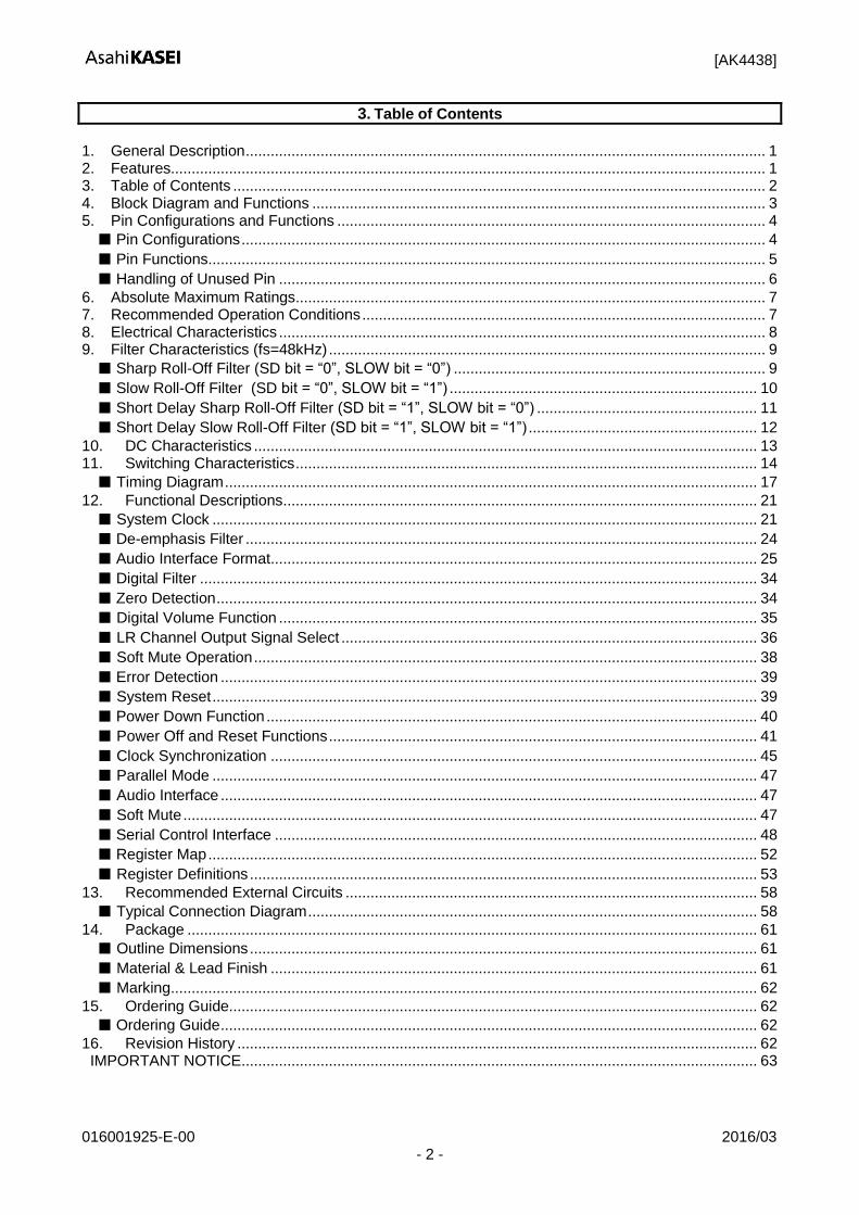
■ Slow Roll-Off Filter (SD bit = “0”, SLOW bit = “1”)
fs=44.1kHz
Parameter Symbol Min. Typ. Max. Unit
Digital Filter
Passband (Note 15) 0.05dB PB 0 8.1 kHz
3.0dB PB 18.2 kHz
Passband Ripple (Note 12) PR -0.043 0.0032 dB
Stopband (Note 15) SB 39.2 kHz
Stopband Attenuation (Note 14) SA 73 dB
Group Delay (Note 13) GD - 6.3 - 1/fs
Digital Filter + SCF + SMF (Note 14)
Frequency Response : 0 20.0kHz -5.06 0.1 dB
fs=96kHz
Parameter Symbol Min. Typ. Max. Unit
Digital Filter
Passband (Note 15) 0.05dB PB 0 17.7 kHz
3.0dB PB 39.5 kHz
Passband Ripple (Note 12) PR -0.043 0.043 dB
Stopband (Note 15) SB 85.3 kHz
Stopband Attenuation (Note 14) SA 73 dB
Group Delay (Note 13) GD - 6.3 - 1/fs
Digital Filter + SCF + SMF (Note 14)
Frequency Response : 0 20.0kHz -5.23 0.1 dB
fs=192kHz
Parameter Symbol Min. Typ. Max. Unit
Digital Filter
Passband (Note 15) 0.05dB PB 0 35.5 kHz
3.0dB PB 79.0 kHz
Passband Ripple (Note 12) PR -0.043 0.043 dB
Stopband (Note 15) SB 171 kHz
Stopband Attenuation (Note 14) SA 73 dB
Group Delay (Note 13) GD - 6.3 - 1/fs
Digital Filter + SCF + SMF (Note 14)
Frequency Response : 0 20.0kHz -5.90 0.1 dB
Note 15. The pass band and stop band frequencies scale with fs. For example, PB=0.185×fs, SB=0.888×fs.
[AK4438]
016001925-E-00 2016/03 - 11 -
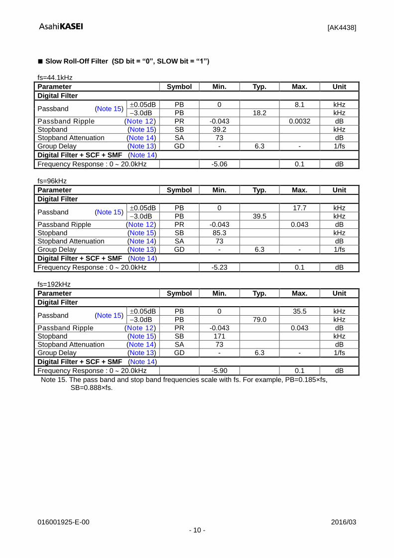
■ Short Delay Sharp Roll-Off Filter (SD bit = “1”, SLOW bit = “0”)
fs=44.1kHz
Parameter Symbol Min. Typ. Max. Unit
Digital Filter
Passband (Note 11) 0.05dB PB 0 20.0 kHz
3.0dB PB 21.5 kHz
Passband Ripple (Note 12) PR -0.0031 0.0031 dB
Stopband (Note 11) SB 24.1 kHz
Stopband Attenuation (Note 14) SA 80 dB
Group Delay (Note 13) GD - 5.8 - 1/fs
Digital Filter + SCF + SMF (Note 14)
Frequency Response : 0 20.0kHz -0.26 0.1 dB
fs=96kHz
Parameter Symbol Min. Typ. Max. Unit
Digital Filter
Passband (Note 11) 0.05dB PB 0 43.5 kHz
3.0dB PB 46.8 kHz
Passband Ripple (Note 12) PR -0.0031 0.0031 dB
Stopband (Note 11) SB 52.5 0 kHz
Stopband Attenuation (Note 14) SA 80 dB
Group Delay (Note 13) GD - 5.8 - 1/fs
Digital Filter + SCF + SMF (Note 14)
Frequency Response : 0 20.0kHz -0.53 0.1 dB
fs=192kHz
Parameter Symbol Min. Typ. Max. Unit
Digital Filter
Passband (Note 11) 0.05dB PB 0 87.0 kHz
3.0dB PB 93.6 kHz
Passband Ripple (Note 12) PR -0.0031 0.0031 dB
Stopband (Note 11) SB 105 kHz
Stopband Attenuation (Note 14) SA 80 dB
Group Delay (Note 13) GD - 5.8 - 1/fs
Digital Filter + SCF + SMF (Note 14)
Frequency Response : 0 20.0kHz -1.9 0.1 dB

[AK4438]
016001925-E-00 2016/03 - 12 -
■ Short Delay Slow Roll-Off Filter (SD bit = “1”, SLOW bit = “1”)
fs=44.1kHz
Parameter Symbol Min. Typ. Max. Unit
Digital Filter
Passband (Note 16) 0.05dB PB 0 11.1 kHz
3.0dB PB 19.4 kHz
Passband Ripple (Note 12) PR -0.05 0.05 dB
Stopband (Note 16) SB 38.1 kHz
Stopband Attenuation (Note 14) SA 82 dB
Group Delay (Note 13) GD - 4.8 - 1/fs
Digital Filter + SCF + SMF (Note 14)
Frequency Response : 0 20.0kHz -5.06 0.1 dB
fs=96kHz
Parameter Symbol Min. Typ. Max. Unit
Digital Filter
Passband (Note 16) 0.05dB PB 0 24.2 kHz
3.0dB PB 42.1 kHz
Passband Ripple (Note 12) PR -0.05 0.05 dB
Stopband (Note 16) SB 83.0 kHz
Stopband Attenuation (Note 14) SA 82 dB
Group Delay (Note 13) GD - 4.8 - 1/fs
Digital Filter + SCF + SMF (Note 14)
Frequency Response : 0 20.0kHz -5.23 0.1 dB
fs=192kH
Parameter Symbol Min. Typ. Max. Unit
Digital Filter
Passband (Note 16) 0.05dB PB 0 48.4 kHz
3.0dB PB 84.3 kHz
Passband Ripple (Note 12) PR -0.05 0.05 dB
Stopband (Note 16) SB 165.9 kHz
Stopband Attenuation (Note 14) SA 82 dB
Group Delay (Note 13) GD - 4.8 - 1/fs
Digital Filter + SCF + SMF (Note 14)
Frequency Response : 0 20.0kHz -5.90 0.1 dB
Note 16. The pass band and stop band frequencies scale with fs. For example, PB=0.252×fs, SB=0.864×fs.

[AK4438]
016001925-E-00 2016/03 - 13 -
10. DC Characteristics
(Ta= -40 +105C; AVDD =3.0 3.6V, TVDD=1.7 3.6V)
Parameter Symbol Min. Typ. Max. Unit
TVDD=1.7V 3.0V
High-Level Input Voltage
Low-Level Input Voltage
VIH1
VIL1
80%TVDD
-
-
-
-
20%TVDD
V
V
TVDD=3.0V 3.6V
High-Level Input Voltage
Low-Level Input Voltage
VIH2
VIL2
70%TVDD
-
-
-
-
30%TVDD
V
V
High-Level Output Voltage (DZF pins: Iout= -100µA)
Low-Level Output Voltage (DZF pin : Iout= 100µA)
(SDA pin, 2.0V TVDD 3.6V: Iout= 3mA)
(SDA pin, 1.7V TVDD 2.0V: Iout= 3mA)
VOH
VOL1
VOL2
VOL3
TVDD0.5
-
-
-
-
-
-
-
0.5
0.4
20%TVDD
V
V
V
V
Input Leakage Current Iin - - 10 A

[AK4438]
016001925-E-00 2016/03 - 14 -
11. Switching Characteristics
(Ta=-40 105C; AVDD=3.0 3.6V, TVDD=1.7 3.6V; CL=20pF, unless otherwise specified.)
Parameter Symbol Min. Typ. Max. Unit
Master Clock Timing
External Clock 256fsn:
Pulse Width Low Pulse Width High
384fsn: Pulse Width Low Pulse Width High
512fsn, 256fsd, 128fsq, 64fso, 32fsh: Pulse Width Low Pulse Width High
768fsn, 384fsd, 192fsq, 96fso, 48fsh: Pulse Width Low Pulse Width High
fCLK tCLKL tCLKH fCLK tCLKL tCLKH fCLK tCLKL tCLKH fCLK tCLKL tCLKH
2.048
32 32
3.072 22 22
4.096 16 16
6.144 11 11
12.288
18.432
24.576
36.864
MHz ns ns
MHz ns ns
MHz ns ns
MHz ns ns
LRCK Timing (Slave mode)
Stereo mode (TDM1-0 bits = “00”) Normal Speed Mode Double Speed Mode Quad Speed Mode Oct speed mode Hex speed mode Duty Cycle
fsn fsd fsq fso fsh Duty
8 48 96
45
384 768
48 96 192
55
kHz kHz kHz kHz kHz %
TDM128 mode (TDM1-0 bits = “01”) LRCK frequency “H” time “L” time
fsn fsd fsq tLRH tLRL
8 48 96
1/128fs 1/128fs
48 96 192
kHz kHz kHz ns ns
TDM256 mode (TDM1-0 bits = “10”) LRCK frequency “H” time “L” time
fsn
fsd tLRH tLRL
8 48
1/256fs 1/256fs
48 96
kHz kHz ns ns
TDM512 mode (TDM1-0 bits = “11”) LRCK frequency “H” time “L” time
fsn tLRH tLRL
8 1/512fs 1/512fs
48
kHz ns ns
[AK4438]
016001925-E-00 2016/03 - 15 -
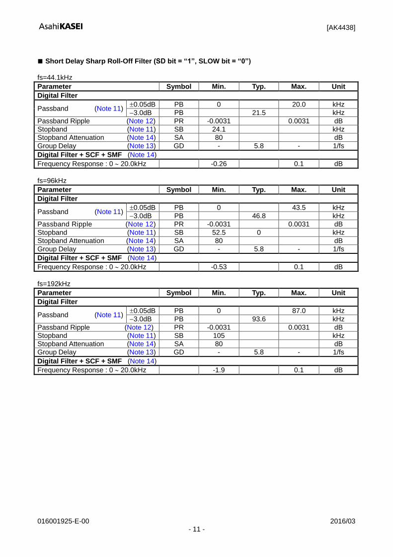
Parameter Symbol Min. Typ. Max. Unit
Audio Interface Timing
Stereo mode (TDM1-0 bits = “00”) BICK Period
Normal Speed Mode Double Speed Mode Quad Speed Mode Oct Speed Mode Hex Speed Mode BICK Pulse Width Low BICK Pulse Width High
LRCK Edge to BICK “” (Note 17)
BICK “” to LRCK Edge (Note 17) SDTI Hold Time SDTI Setup Time
tBCK tBCK tBCK tBCK tBCK tBCKL tBCKH tLRB tBLR tSDH tSDS
1/256fsn 1/128fsd 1/64fsq 1/64fso 1/64fsh
9 9 5 5 5 5
ns ns ns ns ns ns ns ns ns
TDM128 mode (TDM1-0 bits = “01”) BICK Period
Normal Speed Mode Double Speed Mode Quad Speed Mode
BICK Pulse Width Low BICK Pulse Width High
LRCK Edge to BICK “” (Note 17)
BICK “” to LRCK Edge (Note 17) SDTI Hold Time SDTI Setup Time
tBCK tBCK tBCK tBCKL tBCKH tBLR tLRB tSDH tSDS
1/128fsn 1/128fsd 1/128fsq
16 16 5 5 5 5
ns ns ns ns ns ns ns ns ns
TDM256 mode (TDM1-0 bits = “10”) BICK Period
Normal Speed Mode Double Speed Mode
BICK Pulse Width Low BICK Pulse Width High
LRCK Edge to BICK “” (Note 17)
BICK “” to LRCK Edge (Note 17) SDTI Hold Time SDTI Setup Time
tBCK tBCK tBCKL tBCKH tBLR tLRB tSDH tSDS
1/256fsn 1/256fsd
16 16 5 5 5 5
ns ns ns ns ns ns ns ns
TDM512 mode (TDM1-0 bits = “11”) BICK Period
Normal Speed Mode BICK Pulse Width Low BICK Pulse Width High
LRCK Edge to BICK “” (Note 17)
BICK “” to LRCK Edge (Note 17) SDTI Hold Time SDTI Setup Time
tBCK tBCKL tBCKH tBLR tLRB tSDH tSDS
1/512fsn 16 16 5 5 5 5
ns ns ns ns ns ns ns
Note 17. BICK rising edge must not occur at the same time as LRCK edge.
[AK4438]
016001925-E-00 2016/03 - 16 -
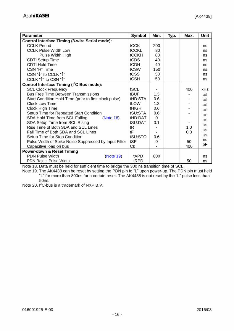
Parameter Symbol Min. Typ. Max. Unit
Control Interface Timing (3-wire Serial mode): CCLK Period CCLK Pulse Width Low
Pulse Width High CDTI Setup Time CDTI Hold Time CSN “H” Time
CSN “” to CCLK “”
CCLK “” to CSN “”
tCCK tCCKL tCCKH tCDS tCDH tCSW tCSS tCSH
200 80 80 40 40
150 50 50
ns ns ns ns ns ns ns ns
Control Interface Timing (I2C Bus mode):
SCL Clock Frequency Bus Free Time Between Transmissions Start Condition Hold Time (prior to first clock pulse) Clock Low Time Clock High Time Setup Time for Repeated Start Condition SDA Hold Time from SCL Falling (Note 18) SDA Setup Time from SCL Rising Rise Time of Both SDA and SCL Lines Fall Time of Both SDA and SCL Lines Setup Time for Stop Condition Pulse Width of Spike Noise Suppressed by Input Filter Capacitive load on bus
fSCL tBUF tHD:STA tLOW tHIGH tSU:STA tHD:DAT tSU:DAT tR tF tSU:STO tSP Cb
-
1.3 0.6 1.3 0.6 0.6 0
0.1 - -
0.6 0 -
400
- - - - - - -
1.0 0.3 -
50 400
kHz
s
s
s
s
s
s
s
s
s ns pF
Power-down & Reset Timing PDN Pulse Width (Note 19) PDN Reject Pulse Width
tAPD tRPD
800
50
ns ns
Note 18. Data must be held for sufficient time to bridge the 300 ns transition time of SCL. Note 19. The AK4438 can be reset by setting the PDN pin to “L” upon power-up. The PDN pin must held
“L” for more than 800ns for a certain reset. The AK4438 is not reset by the “L” pulse less than 50ns.
Note 20. I2C-bus is a trademark of NXP B.V.

[AK4438]
016001925-E-00 2016/03 - 17 -
■ Timing Diagram
1/fCLK
tCLKL
VIH
tCLKH
MCLK VIL
1/fsn, 1/fsd, 1/fsq
LRCK VIH
VIL
tBCK
tBCKL
VIH
tBCKH
BICK VIL
tdLRKL tdLRKH Duty = tdLRKH (or tdLRKL) x fs x 100
Figure 3. Clock Timing (TDM1-0 bits = “00”)
1/fCLK
tCLKL
VIH
tCLKH
MCLK VIL
1/fs
LRCK VIH
VIL
tLRL tLRH
tBCK
tBCKL
VIH
tBCKH
BICK VIL
Figure 4. Clock Timing (Except TDM1-0 bits = “00”)

[AK4438]
016001925-E-00 2016/03 - 18 -
tLRB
LRCK
VIH BICK
VIL
VIH
VIL
tBLR
tSDS
SDTI VIH
VIL
tSDH
Figure 5. Audio Interface Timing (TDM1-0 bits = “00”)
tLRB
LRCK
VIH BICK
VIL
VIH
VIL
tBLR
tSDS
SDTI VIH
VIL
tSDH
Figure 6. Audio Interface Timing (Except TDM1-0 bits = “00”)
[AK4438]
016001925-E-00 2016/03 - 19 -
CSNVIH
VIL
tCSS
CCLK
tCDS
VIH
VIL
CDTIVIH
tCCKHtCCKL
tCDH
VILC1 C0 R/W
tCSH
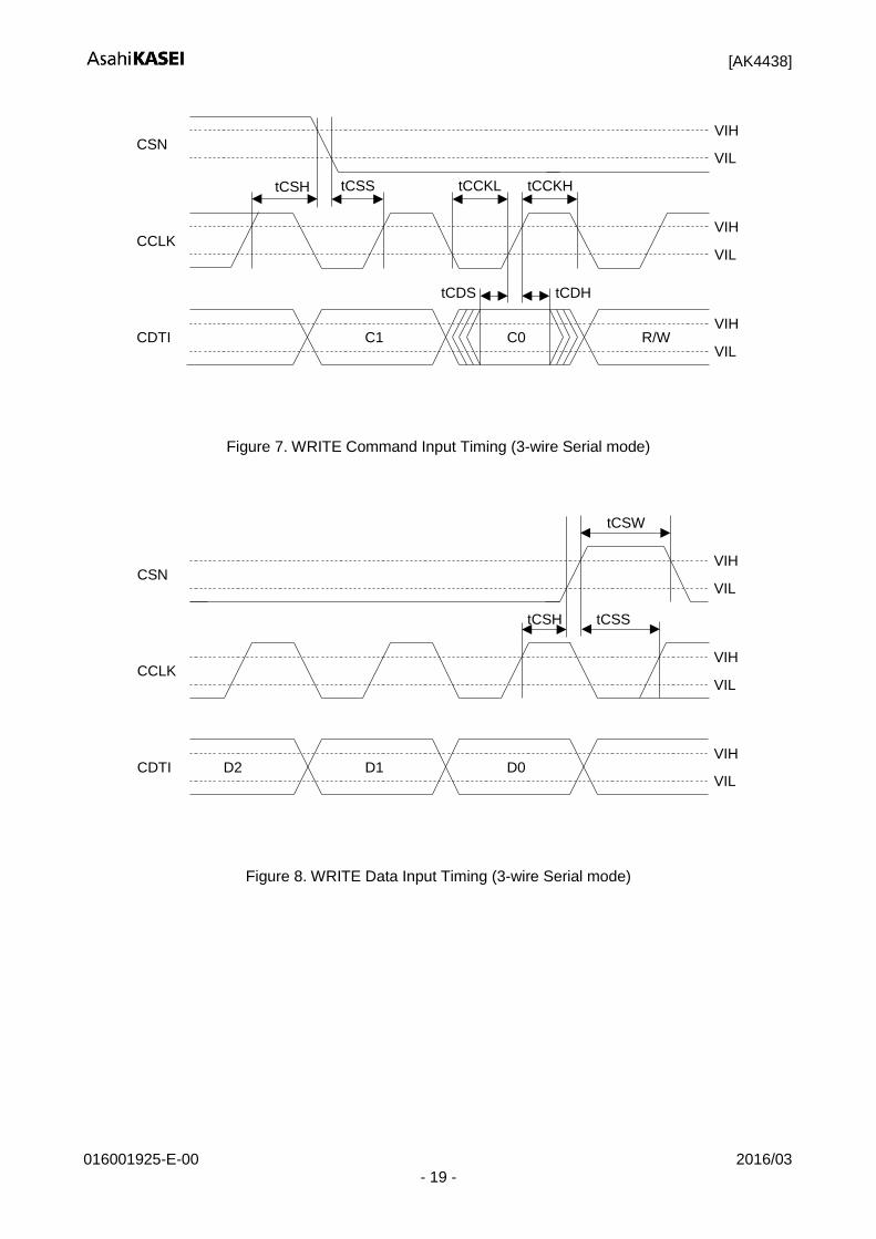
Figure 7. WRITE Command Input Timing (3-wire Serial mode)
CSNVIH
VIL
tCSH
CCLKVIH
VIL
CDTIVIH
tCSW
VILD1 D0D2
tCSS
Figure 8. WRITE Data Input Timing (3-wire Serial mode)

[AK4438]
016001925-E-00 2016/03 - 20 -
tHIGH
SCL
SDA
VIH
tLOWtBUF
tHD:STA
tR tF
tHD:DAT tSU:DAT tSU:STA
Stop Start Start Stop
tSU:STO
VIL
VIH
VIL
tSP
Figure 9. I2C Bus mode Timing
tAPD
PDNVIL
tRPD
Figure 10. Power-down & Reset Timing

[AK4438]
016001925-E-00 2016/03 - 21 -
12. Functional Descriptions
■ System Clock
The external clocks which are required to operate the AK4438 are MCLK, LRCK and BICK. MCLK should be synchronized with LRCK and BICK but the phase is not critical. There are two methods to set MCLK frequency. In Manual Setting Mode (ACKS bit= “0”: Default), the sampling speed is set by DFS2-0 bit (Table 1). The frequency of MCLK at each sampling speed is set automatically (Table 2, Table 3). In Auto Setting Mode (ACKS bit= “1”), as MCLK frequency is detected automatically (Table 4) and the internal master clock attains the appropriate frequency (Table 5), so it is not necessary to set DFS2-0 bits. After exiting reset at power-up (PDN pin = “L” →“H”), the AK4438 is in power-down mode until MCLK and LRCK are input. The AK4438 is set to Manual Setting Mode at power-up (PDN pin = “L” →“H”). When changing the clock, the AK4438 must be reset by the PDN pin or RSTN bit. If the clock is stopped, a click noise occurs when restarting the clock. Mute the digital output externally if the click noise affects system applications.

[AK4438]
016001925-E-00 2016/03 - 22 -
1. Manual Setting Mode (ACKS bit = “0”)
MCLK frequency is detected automatically and the sampling rate is set by DFS2-0 bits (Table 1). The MCLK frequency corresponding to each sampling speed should be provided externally (Table 2, Table 3). The AK4438 is set to Manual Setting Mode at power-up (PDN pin = “L” →“H”). When DFS2-0 bits are changed, the AK4438 should be reset by RSTN bit.
DFS2 DFS1 DFS0 Sampling Speed Mode (fs) (default) 0 0 0 Normal Speed Mode 8kHz~48kHz
0 0 1 Double Speed Mode 48kHz~96kHz
0 1 0 Quad Speed Mode 96kHz~192kHz
0 1 1 N/A N/A
1 0 0 Oct Speed Mode 384kHz
1 0 1 Hex Speed Mode 768kHz
1 1 0 N/A N/A
1 1 1 N/A N/A
(N/A: Not Available)
Table 1. Sampling Speed (Manual Setting Mode)
LRCK MCLK(MHz) Sampling Speed fs 32fs 48fs 64fs 96fs
8.0kHz N/A N/A N/A N/A
Normal 44.1kHz N/A N/A N/A N/A
48.0kHz N/A N/A N/A N/A
88.2kHz N/A N/A N/A N/A Double
96.0kHz N/A N/A N/A N/A
176.4kHz N/A N/A N/A N/A Quad
192.0kHz N/A N/A N/A N/A
384.0kHz N/A N/A 24.576 36.864 Oct
768.0kHz 24.576 36.864 N/A N/A Hex
Table 2. System Clock Example (Manual Setting Mode)
LRCK MCLK(MHz) Sampling Speed fs 128fs 192fs 256fs 384fs 512fs 768fs
8.0kHz N/A N/A 2.0480 3.0720 4.0960 6.1440
Normal 44.1kHz N/A N/A 11.2896 16.9344 22.5792 33.8688
48.0kHz N/A N/A 12.2880 18.4320 24.5760 36.8640
88.2kHz N/A N/A 22.5792 33.8688 N/A N/A Double
96.0kHz N/A N/A 24.5760 36.8640 N/A N/A
176.4kHz 22.5792 33.8688 N/A N/A N/A N/A Quad
192.0kHz 24.5760 36.8640 N/A N/A N/A N/A
384.0kHz N/A N/A N/A N/A N/A N/A Oct
768.0kHz N/A N/A N/A N/A N/A N/A Hex
Table 3. System Clock Example (Manual Setting Mode)

[AK4438]
016001925-E-00 2016/03 - 23 -
2. Auto Setting Mode (ACKS bit = “1”)
MCLK frequency and the sampling speed are detected automatically (Table 4) and DFS2-0 bits are ignored. The MCLK frequency corresponding to each sampling speed should be provided externally (Table 5, Table 6).
MCLK Sampling Speed Mode
512fs/256fs 768fs/384fs Normal Speed Mode
256fs 384fs Double Speed Mode
128fs 192fs Quad Speed Mode
64fs 96fs Oct Speed Mode
32fs 48fs Hex Speed Mode
Table 4. Sampling Speed (Auto Setting Mode)
LRCK MCLK(MHz) Sampling Speed fs 32fs 48fs 64fs 96fs
8.0kHz N/A N/A N/A N/A
Normal 44.1kHz N/A N/A N/A N/A
48.0kHz N/A N/A N/A N/A
88.2kHz N/A N/A N/A N/A Double
96.0kHz N/A N/A N/A N/A
176.4kHz N/A N/A N/A N/A Quad
192.0kHz N/A N/A N/A N/A
384.0kHz N/A N/A 24.576 36.864 Oct
768.0kHz 24.576 36.864 N/A N/A Hex
Table 5. System Clock Example (Auto Setting Mode)
LRCK MCLK(MHz) Sampling Speed fs 128fs 192fs 256fs 384fs 512fs 768fs
8.0kHz N/A N/A 2.0480 3.0720 4.0960 6.1440
Normal 44.1kHz N/A N/A 11.2896 16.9344 22.5792 33.8688
48.0kHz N/A N/A 12.2880 18.4320 24.5760 36.8640
88.2kHz N/A N/A 22.5792 33.8688 N/A N/A Double
96.0kHz N/A N/A 24.5760 36.8640 N/A N/A
176.4kHz 22.5792 33.8688 N/A N/A N/A N/A Quad
192.0kHz 24.5760 36.8640 N/A N/A N/A N/A
384.0kHz N/A N/A N/A N/A N/A N/A Oct
768.0kHz N/A N/A N/A N/A N/A N/A Hex
Table 6. System Clock Example (Auto Setting Mode)
MCLK= 256fs/384fs supports sampling rate of 8kHz~96kHz (Table 7). However, when the sampling rate is 8kHz~48kHz, DR and S/N will degrade by approximately 3dB as compared to when MCLK= 512fs/768fs.
ACKS bit MCLK DR,S/N
L 256fs/384fs/512fs/768fs 108dB
H 256fs/384fs 105dB
H 512fs/768fs 108dB
Table 7. Relationship of DR, S/N and MCLK frequency (fs = 44.1kHz)

[AK4438]
016001925-E-00 2016/03 - 24 -
■ De-emphasis Filter
The AK4438 has a digital de-emphasis filter (tc=50/15µs) by an IIR filter. The de-emphasis filter only supports Normal Speed Mode. This filter corresponds to three sampling frequencies (32kHz, 44.1kHz, 48kHz). De-emphasis of each DAC can be set individually for DAC1(SDTI1), DAC2(SDTI2), DAC3(SDTI3) and DAC4(SDTI4) by register settings.
Mode Sampling Speed Mode
DEM11 (DEM41-21)
DEM10 (DEM40-20)
DEM
0 Normal Speed Mode 0 0 44.1kHz
1 Normal Speed Mode 0 1 OFF (default)
2 Normal Speed Mode 1 0 48kHz
3 Normal Speed Mode 1 1 32kHz
Table 8. De-emphasis Control

[AK4438]
016001925-E-00 2016/03 - 25 -
■ Audio Interface Format
TDM1-0 bits, DIF2-0 bits, SDS2-0 bits, TDM1-0 pins and DIF pin settings should not be changed during operation. [1] PCM Mode Normal Mode (TDM1-0 bit=“00”) Eight channels audio data is shifted in via the SDTI1-4 pins using BICK and LRCK inputs. Data is selected by SDS2-0 bits. Eight data formats are supported and selected by the DIF2-0 bits as shown in Table 9. In all formats the serial data is MSB first, 2's compliment format and is latched on the rising edge of BICK. Mode 2 can be used in 16-bit and 20-bit MSB justified and Mode 6 can be used in 16-bit, 20-bit and 24-bit MSB justified formats by zeroing the unused LSBs. TDM128 Mode (TDM1-0 bit=“01”) Eight channels audio data is shifted in via the SDTI1-2 pins using BICK and LRCK inputs. Data is selected by SDS2-0 bits. The data input to the SDTI3-4 pins are ignored. BICK is fixed to 128fs. Six data formats are supported and selected by the DIF2-0 bits as shown in Table 9. In all formats the serial data is MSB first, 2's compliment format and is latched on the rising edge of BICK. TDM256 Mode (TDM1-0 bit=“10”) Sixteen channels audio data is shifted in via the SDTI1-2 pins using BICK and LRCK inputs. Data is selected by SDS2-0 bits. The data input to the SDTI3-4 pins are ignored. BICK is fixed to 256fs. Six data formats are supported and selected by the DIF2-0 bits as shown in Table 9. In all formats the serial data is MSB first, 2's compliment format and is latched on the rising edge of BICK. TDM512 Mode (TDM1-0 bit=“11”) Sixteen channels audio data is shifted in via the SDTI1 pin using BICK and LRCK inputs. Data is selected by SDS2-0 bits. The data input to the SDTI2-4 pins are ignored. BICK is fixed to 512fs. Six data formats are supported and selected by the DIF2-0 bits as shown in Table 9. In all formats the serial data is MSB first, 2's compliment format and is latched on the rising edge of BICK.

[AK4438]
016001925-E-00 2016/03 - 26 -
Mode TDM1 TDM0 DIF2 DIF1 DIF0 SDTI Format LRCK BICK
Normal (Note 21)
0
0 0
0 0 0 16-bit LSB justified H/L 32fs
1 0 0 1 20-bit LSB justified H/L 40fs
2 0 1 0 24-bit MSB justified H/L 48fs
3 0 1 1 16-bit I
2S compatible L/H 32fs
24-bit I2S compatible L/H 48fs
4 1 0 0 24-bit LSB justified H/L 48fs
5 1 0 1 32-bit LSB justified H/L 64fs
6 1 1 0 32-bit MSB justified H/L 64fs
7 1 1 1 32-bit I2S compatible L/H 64fs
TDM128
-
0 1
0 0 0 N/A 128fs
- 0 0 1 N/A 128fs
8 0 1 0 24-bit MSB justified 128fs
9 0 1 1 24-bit I2S compatible 128fs
10 1 0 0 24-bit LSB justified 128fs
11 1 0 1 32-bit LSB justified 128fs
12 1 1 0 32-bit MSB justified 128fs
13 1 1 1 32-bit I2S compatible 128fs
TDM256
-
1 0
0 0 0 N/A 256fs
- 0 0 1 N/A 256fs
14 0 1 0 24-bit MSB justified 256fs
15 0 1 1 24-bit I2S compatible 256fs
16 1 0 0 24-bit LSB justified 256fs
17 1 0 1 32-bit LSB justified 256fs
18 1 1 0 32-bit MSB justified 256fs
19 1 1 1 32-bit I2S compatible 256fs
TDM512
-
1 1
0 0 0 N/A 512fs
- 0 0 1 N/A 512fs
20 0 1 0 24-bit MSB justified 512fs
21 0 1 1 24-bit I2S compatible 512fs
22 1 0 0 24-bit LSB justified 512fs
23 1 0 1 32-bit LSB justified 512fs
24 1 1 0 32-bit MSB justified 512fs
25 1 1 1 32-bit I2S compatible 512fs
Note 21. BICK that is input to each channel must be longer than the bit length of setting format. (N/A: Not available)
Table 9. Audio Data Format

[AK4438]
016001925-E-00 2016/03 - 27 -
SDTI1-4
BICK
LRCK
SDTI1-4 15 14 6 5 4
BICK
0 1 10 11 12 13 14 15 0 1 10 11 12 13 14 15 0 1
3 2 1 0 15 14
(32fs)
(64fs)
0 14 1 15 16 17 31 0 1 14 15 16 17 31 0 1
15 14 0 15 14 0 Mode 0
Don’t care Don’t care
15:MSB, 0:LSB
Mode 0
15 14 6 5 4 3 2 1 0
Lch Data Rch Data
Figure 11. Mode 0 Timing
SDTI1-4
LRCK
BICK
(64fs)
0 9 1 10 11 12 31 0 1 9 10 11 12 31 0 1
19 0 19 0 Mode 1
Don’t care Don’t care
19:MSB, 0:LSB
SDTI1-4 Mode 4
23:MSB, 0:LSB
20 19 0 20 19 0 Don’t care Don’t care 22 21 22 21
Lch Data Rch Data
8
23 23
8
Figure 12. Mode 1/4 Timing
LRCK
BICK
(64fs)
SDTI1-4
0 22 1 2 24 31 0 1 31 0 1
23:MSB, 0:LSB
22 1 0 Don’t care 23
Lch Data Rch Data
23 30 22 2 24 23 30
22 1 0 Don’t care 23 22 23
Figure 13. Mode 2 Timing

[AK4438]
016001925-E-00 2016/03 - 28 -
LRCK
BICK
(64fs)
SDTI1-4
0 3 1 2 24 31 0 1 31 0 1
23:MSB, 0:LSB
22 1 0 Don’t care 23
Lch Data Rch Data
23 25 3 2 24 23 25
22 1 0 Don’t care 23 23
Figure 14. Mode 3 Timing
LRCK
BICK
(64fs)
SDTI1-4
0 22 1 2 24 31 0 1 31 0 1
32:MSB, 0:LSB
30 1 0 31
Lch Data Rch Data
23 30 22 2 24 23 30
30 1 0 31 30 31
Mode 5,6
Figure 15. Mode 5/6 Timing
LRCK
BICK
(64fs)
SDTI1-4
0 3 1 2 24 31 0 1 31 0 1
32:MSB, 0:LSB
30 1 0 31
Lch Data Rch Data
23 25 3 2 24 23 25
30 1 0 31 30 31
Figure 16. Mode 7 Timing
[AK4438]
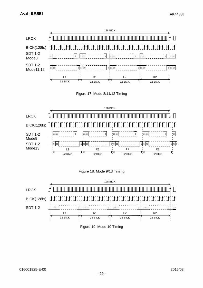
016001925-E-00 2016/03 - 29 -
LRCK
BICK(128fs)
128 BICK
L1
32 BICK
R1
32 BICK
L2
32 BICK
R2
32 BICK
SDTI1-2 22 0 22 0 22 0 22 0 23 23 23 23 22 23
Mode8
SDTI1-2 30 0 30 0 30
2
0 30 0 31 31 31 31 30 31
Mode11,12
Figure 17. Mode 8/11/12 Timing
LRCK
BICK(128fs)
128 BICK
L1
32 BICK
R1
32 BICK
L2
32 BICK
R2
32 BICK
SDTI1-2 22 0 22 0 22 0 22 0 23 23 23 23 23
SDTI1-2
Mode9
Mode13
30 0 30 0 30
2
0 30 0 31 31 31 31 30 31
Figure 18. Mode 9/13 Timing
LRCK
BICK(128fs)
128 BICK
L1
32 BICK
R1
32 BICK
L2
32 BICK
R2
32 BICK
SDTI1-2 22 0 22 0 22 0 22 0 23 23 23 23 23
Figure 19. Mode 10 Timing

[AK4438]
016001925-E-00 2016/03 - 30 -
23
LRCK
BICK (256fs)
22 0
L1
32 BICK
256 BICK
22 0
R1
32 BICK
22 23 23 22 0
L2
32 BICK
22 0
R2
32 BICK
23 23 SDTI1-2
31 30 0 30 31 31 30 0 31 30 0 31 30 0 SDTI1-2
Mode14
Mode17,18
23 22 0
L3
32 BICK
22 0
R3
32 BICK
23 22 0
L4
32 BICK
22 0
R4
32 BICK
23 23
31 30 0 31 30 0 31 30 0 31 30 0
Figure 20. Mode 14/17/18 Timing
LRCK
BICK (256fs)
23 0
L1
32 BICK
256 BICK
23 0
R1
32 BICK
23 23 0
L2
32 BICK
23 0
R2
32 BICK
SDTI1-2 Mode15
31 0 31 30 31 0 30 31 0 30 31 0 30 SDTI1-2 Mode19
23 0
L3
32 BICK
23 0
R3
32 BICK
23 0
L4
32 BICK
23 0
R4
32 BICK
31 0 30 31 0 30 31 0 30 31 0 30
Figure 21. Mode 15/19 Timing
LRCK
BICK(256fs)
SDTI1-2
256 BICK
22 0
L1
32 BICK
22 0
R1
32 BICK
22 0
L2
32 BICK
22 0
R2
32 BICK
23 23 23 23 23 22 0
L3
32 BICK
22 0
R3
32 BICK
22 0
L4
32 BICK
22 0
R4
32 BICK
23 23 23 23
Figure 22. Mode 16 Timing

[AK4438]
016001925-E-00 2016/03 - 31 -
BICK(512fs)
SDTI1
Mode8
LRCK
512BICK
22
0 23
22
0 23
22
0 23
22
0 23
22
2
0 23 22
0 23
22
0 23
22 0 23
SDTI1
Mode11,12 L1 32 BICK
R1 32 BICK
L2 32 BICK
R2 32 BICK
L3 32 BICK
R3 32 BICK
L4 32 BICK
R4 32 BICK 32 BICK 32 BICK 32 BICK 32 BICK 32 BICK 32 BICK 32 BICK 32 BICK
22 0 31
23
22 0 31 22 0 31 22 0 31 22 0 31 22 0 31 22 0 31 22 0 31 31
Figure 23. Mode 20/23/24 Timing
BICK(512fs)
SDTI1
Mode21
LRCK
512BICK
22
0 23
22
0 23
22
0 23
22
0 23
22
2
0 23 22
0 23
22
0 23
22 0 23
SDTI1
Mode25 L1 32 BICK
R1 32 BICK
L2 32 BICK
R2 32 BICK
L3 32 BICK
R3 32 BICK
L4 32 BICK
R4 32 BICK 32 BICK 32 BICK 32 BICK 32 BICK 32 BICK 32 BICK 32 BICK 32 BICK
22 0 31
23
22 0 31 22 0 31 22 0 31 22 0 31 22 0 31 22 0 31 22 0 31 31
Figure 24. Mode 21/25 Timing
BICK(512fs)
SDTI1
Mode22
LRCK
512BICK
22
0 23
22
0 23
22
0 23
22
0 23
22
2
0 23 22
0 23
22
0 23
22 0 23
L1 32 BICK
R1 32 BICK
L2 32 BICK
R2 32 BICK
L3 32 BICK
R3 32 BICK
L4 32 BICK
R4 32 BICK 32 BICK 32 BICK 32 BICK 32 BICK 32 BICK 32 BICK 32 BICK 32 BICK
23
Figure 25. Mode 22 Timing

[AK4438]
016001925-E-00 2016/03 - 32 -
[2] Data Select SDS2-0 bits control the playback channel of each DAC.
LRCK
SDTI1 R1 L1
SDTI2 R2 L2
SDTI3 R3 L3
SDTI4 R4 L4
Figure 26. Data Slot in Normal Mode
SDTI1 R1 L1
SDTI2
LRCK
128 BICK
R2 L2
R3 L3 R4 L4
Figure 27. Data Slot in TDM128 Mode
SDTI1 R1 L1
LRCK
256 BICK
R2 L2 R3 L3 R4 L4
SDTI2 R5 L5 R6 L6 R7 L7 R8 L8
Figure 28. Data Slot in TDM256 Mode
SDTI1 R1 L1
LRCK
512 BICK
R2 L2 R3 L3 R4 L4 R5 R6 L6 R7 L7 R8 L8 L5
Figure 29. Data Slot in TDM512 Mode

[AK4438]
016001925-E-00 2016/03 - 33 -
SDS2 SDS1 SDS0 DAC1 DAC2 DAC3 DAC4
Lch Rch Lch Rch Lch Rch Lch Rch
Normal
* 0 0 L1 R1 L2 R2 L3 R3 L4 R4
* 0 1 L2 R2 L3 R3 L4 R4 L1 R1
* 1 0 L3 R3 L4 R4 L1 R1 L2 R2
* 1 1 L4 R4 L1 R1 L2 R2 L3 R3
TDM128
* 0 0 L1 R1 L2 R2 L3 R3 L4 R4
* 0 1 L2 R2 L3 R3 L4 R4 L1 R1
* 1 0 L3 R3 L4 R4 L1 R1 L2 R2
* 1 1 L4 R4 L1 R1 L2 R2 L3 R3
TDM256
0 0 0 L1 R1 L2 R2 L3 R3 L4 R4
0 0 1 L2 R2 L3 R3 L4 R4 L5 R5
0 1 0 L3 R3 L4 R4 L5 R5 L6 R6
0 1 1 L4 R4 L5 R5 L6 R6 L7 R7
1 0 0 L5 R5 L6 R6 L7 R7 L8 R8
1 0 1 L6 R6 L7 R7 L8 R8 L1 R1
1 1 0 L7 R7 L8 R8 L1 R1 L2 R2
1 1 1 L8 R8 L1 R1 L2 R2 L3 R3
TDM512
0 0 0 L1 R1 L2 R2 L3 R3 L4 R4
0 0 1 L2 R2 L3 R3 L4 R4 L5 R5
0 1 0 L3 R3 L4 R4 L5 R5 L6 R6
0 1 1 L4 R4 L5 R5 L6 R6 L7 R7
1 0 0 L5 R5 L6 R6 L7 R7 L8 R8
1 0 1 L6 R6 L7 R7 L8 R8 L1 R1
1 1 0 L7 R7 L8 R8 L1 R1 L2 R2
1 1 1 L8 R8 L1 R1 L2 R2 L3 R3
(*: Do not care) Table 10. Data Select

[AK4438]
016001925-E-00 2016/03 - 34 -
■ Digital Filter
Five digital filters are available for playback, providing a choice of different sound colors. These digital filters are selected by SD bit, SLOW bit and SSLOW bit.
SSLOW SD bit SLOW bit Mode
0 0 0 Sharp roll-off filter
0 0 1 Slow roll-off filter
0 1 0 Short delay Sharp roll-off filter (default)
0 1 1 Short delay Slow roll-off filter
1 * * Super Slow Roll-off Mode
Table 11. Digital Filter Setting (*: don’t care)
■ Zero Detection
The AK4438 has channel-independent zero detection function. Zero detection channels (AOUTL1-4 and AOUTR1-4 pins) can be selected by 07H/08H registers (L1-4 bits, R1-4 bits). When the input data at each channel is continuously zeros for 8192 LRCK cycles, the DZF pin goes to “H”. The DZF pin immediately returns to “L” if the input data of each channel is not zero. If the RSTN bit is “0”, the DZF pins of both channels go to “H”. The DZF pin of both channels go to “L” after 4 ~ 5/fs when RSTN bit returns to “1”. The DZFB bit can invert the polarity of the DZF pin. If all channels are disabled, the DZF pin outputs “Not zero”.
DZFB bit Data DZF pin
0 Not zero L
Zero detect H
1 Not zero H
Zero detect L
Not zero: One of the zero detection channels set by L1-4 bits and R1-4 bits does not detect zero. Zero detect: All zero detection channels set by L1-4 bits and R1-4 bits detect zero.
Table 12. DZF Pin Function
[AK4438]
016001925-E-00 2016/03 - 35 -
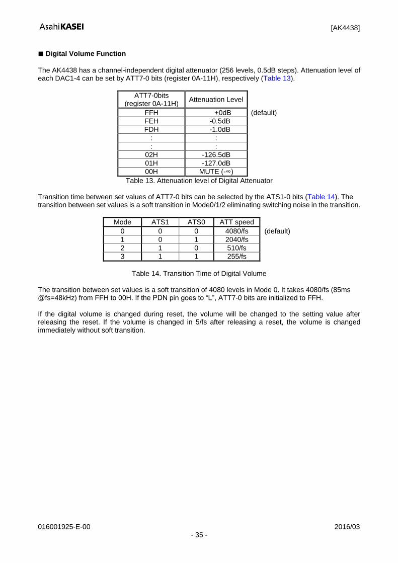
■ Digital Volume Function
The AK4438 has a channel-independent digital attenuator (256 levels, 0.5dB steps). Attenuation level of each DAC1-4 can be set by ATT7-0 bits (register 0A-11H), respectively (Table 13).
ATT7-0bits (register 0A-11H)
Attenuation Level
FFH +0dB (default)
FEH -0.5dB
FDH -1.0dB
: :
: :
02H -126.5dB
01H -127.0dB
00H MUTE (-∞)
Table 13. Attenuation level of Digital Attenuator Transition time between set values of ATT7-0 bits can be selected by the ATS1-0 bits (Table 14). The transition between set values is a soft transition in Mode0/1/2 eliminating switching noise in the transition.
Mode ATS1 ATS0 ATT speed
0 0 0 4080/fs (default)
1 0 1 2040/fs
2 1 0 510/fs
3 1 1 255/fs
Table 14. Transition Time of Digital Volume
The transition between set values is a soft transition of 4080 levels in Mode 0. It takes 4080/fs (85ms @fs=48kHz) from FFH to 00H. If the PDN pin goes to “L”, ATT7-0 bits are initialized to FFH. If the digital volume is changed during reset, the volume will be changed to the setting value after releasing the reset. If the volume is changed in 5/fs after releasing a reset, the volume is changed immediately without soft transition.

[AK4438]
016001925-E-00 2016/03 - 36 -
■ LR Channel Output Signal Select
Input and output signal combination of the AK4438 can be set by MONO1-4 bits and SELLR1-4 bits. The output signal phase of DAC is controlled by INVL1-4 and INVR1-4 bits. These settings are available for any audio format.
MONO1 bit SELLR1 bit INVL1 bit INVR1 bit L1ch Out R1ch Out
0 0
0 0 L1ch In R1ch In
1 0 L1ch In Invert R1ch In
0 1 L1ch In R1ch In Invert
1 1 L1ch In Invert R1ch In Invert
0 1
0 0 R1ch In L1ch In
1 0 R1ch In Invert L1ch In
0 1 R1ch In L1ch In Invert
1 1 R1ch In Invert L1ch In Invert
1 0
0 0 L1ch In L1ch In
1 0 L1ch In Invert L1ch In
0 1 L1ch In L1ch In Invert
1 1 L1ch In Invert L1ch In Invert
1 1
0 0 R1ch In R1ch In
1 0 R1ch In Invert R1ch In
0 1 R1ch In R1ch In Invert
1 1 R1ch In Invert R1ch In Invert
Table 15. Output Select for DAC1
MONO2 bit SELLR2 bit INVL2 bit INVR2 bit L2ch Out R2ch Out
0 0
0 0 L2ch In R2ch In
1 0 L2ch In Invert R2ch In
0 1 L2ch In R2ch In Invert
1 1 L2ch In Invert R2ch In Invert
0 1
0 0 R2ch In L2ch In
1 0 R2ch In Invert L2ch In
0 1 R2ch In L2ch In Invert
1 1 R2ch In Invert L2ch In Invert
1 0
0 0 L2ch In L2ch In
1 0 L2ch In Invert L2ch In
0 1 L2ch In L2ch In Invert
1 1 L2ch In Invert L2ch In Invert
1 1
0 0 R2ch In R2ch In
1 0 R2ch In Invert R2ch In
0 1 R2ch In R2ch In Invert
1 1 R2ch In Invert R2ch In Invert
Table 16. Output Select for DAC2
[AK4438]
016001925-E-00 2016/03 - 37 -
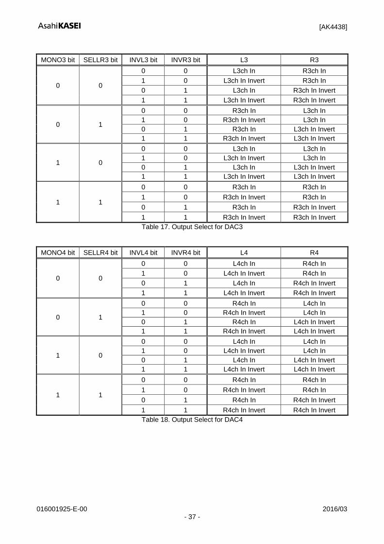
MONO3 bit SELLR3 bit INVL3 bit INVR3 bit L3 R3
0 0
0 0 L3ch In R3ch In
1 0 L3ch In Invert R3ch In
0 1 L3ch In R3ch In Invert
1 1 L3ch In Invert R3ch In Invert
0 1
0 0 R3ch In L3ch In
1 0 R3ch In Invert L3ch In
0 1 R3ch In L3ch In Invert
1 1 R3ch In Invert L3ch In Invert
1 0
0 0 L3ch In L3ch In
1 0 L3ch In Invert L3ch In
0 1 L3ch In L3ch In Invert
1 1 L3ch In Invert L3ch In Invert
1 1
0 0 R3ch In R3ch In
1 0 R3ch In Invert R3ch In
0 1 R3ch In R3ch In Invert
1 1 R3ch In Invert R3ch In Invert
Table 17. Output Select for DAC3
MONO4 bit SELLR4 bit INVL4 bit INVR4 bit L4 R4
0 0
0 0 L4ch In R4ch In
1 0 L4ch In Invert R4ch In
0 1 L4ch In R4ch In Invert
1 1 L4ch In Invert R4ch In Invert
0 1
0 0 R4ch In L4ch In
1 0 R4ch In Invert L4ch In
0 1 R4ch In L4ch In Invert
1 1 R4ch In Invert L4ch In Invert
1 0
0 0 L4ch In L4ch In
1 0 L4ch In Invert L4ch In
0 1 L4ch In L4ch In Invert
1 1 L4ch In Invert L4ch In Invert
1 1
0 0 R4ch In R4ch In
1 0 R4ch In Invert R4ch In
0 1 R4ch In R4ch In Invert
1 1 R4ch In Invert R4ch In Invert
Table 18. Output Select for DAC4

[AK4438]
016001925-E-00 2016/03 - 38 -
■ Soft Mute Operation
The soft mute operation is performed at digital domain. When the SMUTE pin goes to “H” or set SMUTE
bit to “1”, the output signal is attenuated by during ATT_DATA ATT transition time from the current ATT level. When the SMUTE pin is returned to “L” or the SMUTE bit is returned to “0”, the mute is
cancelled and the output attenuation gradually changes to the ATT level during ATT_DATA ATT
transition time. If the soft mute is cancelled before attenuating , the attenuation is discontinued and returned to ATT level by the same cycle. The soft mute is effective for changing the signal source without stopping the signal transmission.
SMUTE pin or SMUTE bit
Attenuation
DZF pin
ATT_Level
-
AOUT
8192/fs
GD GD
(1)
(2)
(3)
(4)
(1)
(2)
Notes:
(1) ATT_DATA ATT transition time. For example, this time is 4080LRCK cycles at ATT_DATA=255 in Normal Speed Mode.
(2) The analog output corresponding to the digital input has group delay (GD).
(3) If the soft mute is cancelled before attenuating after starting the operation, the attenuation is discontinued and returned to ATT level by the same cycle.
(4) When the input data for a zero detection channel is continuously zeros for 8192 LRCK cycles, the DZF pin goes to “H”. The DZF pin immediately returns to “L” if input data are not zero.
Figure 30. Soft Mute Function and Zero Detection

[AK4438]
016001925-E-00 2016/03 - 39 -
■ Error Detection
Three types of error can be detected in I
2C mode when the LDOE pin = “H”. (Table 19).When the error is
detected, LDO is powered down and writing into the control registers is prohibited. Once the error is detected the AK4438 does not return to normal operation automatically even if the error condition is removed so restart the AK4438 by the PDN pin. In I
2C mode, the AK4438 does not generate
acknowledge (ACK) in error status.
No Error Error Condition
1 Internal Reference Voltage Error Internal reference voltage is not powered up.
2 LDO Over Voltage Detection LDO voltage > 1.5V (typ.)
3 LDO Over Current Detection LDO current < 51mA (typ.)
Table 19. Error Detection
■ System Reset The AK4438 should be reset once by bringing the PDN pin = “L” upon power-up. Power-down state of the reference voltage such as LDO and VCOM will be released by PDN pin = “H” and writing into resisters is valid in 1ms. The AK4438 is in power-down state until MCLK and LRCK input.

[AK4438]
016001925-E-00 2016/03 - 40 -
■ Power Down Function
The AK4438 is placed in power-down mode by bringing the PDN pin “L” and the analog outputs become floating (Hi-Z) state. Power-up and power-down timings are shown in Figure 31.
PDN pin
Power
Reset Normal Operation (Register Write and DAC input are available)
Clock In MCLK,LRCK,BICK
DAC In (Digital)
DAC Out (Analog)
External Mute
Mute ON (7)
DZF
Don’t care
“0”data
GD (3)
(5)
(6)
(8)
GD
(5)
Mute ON
“0”data
Don’t care
Internal State
(4) (4)
(1)
Internal PDN (2)
LDOO pin
Notes:
(1) After AVDD and TVDD are powered-up, the PDN pin should be “L” for 800ns.
(2) After PDN pin = “H”, the internal LDO and VCOM power-up. The internal registers are initialized. Register writing is available in 1msec after PDN pin = “H”.
(3) The analog output corresponding to digital input has group delay (GD).
(4) Analog outputs are floating (Hi-Z) in power down mode.
(5) Click noise occurs at an edge of PDN signal. This noise is output even if “0” data is input.
(6) MCLK, BICK and LRCK clocks can be stopped in power-down mode (PDN pin= “L”). (7) Mute the analog output externally if click noise (5) adversely affect system performance
The timing example is shown in this figure.
(8) The DZF pin outputs “L” in internal power-down mode.
Figure 31. Pin Power Down/Up Sequence Example
[AK4438]
016001925-E-00 2016/03 - 41 -
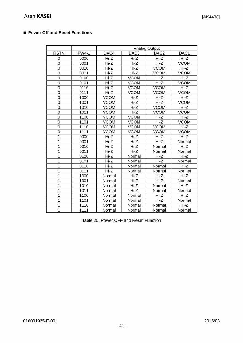
■ Power Off and Reset Functions
Analog Output
RSTN PW4-1 DAC4 DAC3 DAC2 DAC1
0 0000 Hi-Z Hi-Z Hi-Z Hi-Z
0 0001 Hi-Z Hi-Z Hi-Z VCOM
0 0010 Hi-Z Hi-Z VCOM Hi-Z
0 0011 Hi-Z Hi-Z VCOM VCOM
0 0100 Hi-Z VCOM Hi-Z Hi-Z
0 0101 Hi-Z VCOM Hi-Z VCOM
0 0110 Hi-Z VCOM VCOM Hi-Z
0 0111 Hi-Z VCOM VCOM VCOM
0 1000 VCOM Hi-Z Hi-Z Hi-Z
0 1001 VCOM Hi-Z Hi-Z VCOM
0 1010 VCOM Hi-Z VCOM Hi-Z
0 1011 VCOM Hi-Z VCOM VCOM
0 1100 VCOM VCOM Hi-Z Hi-Z
0 1101 VCOM VCOM Hi-Z VCOM
0 1110 VCOM VCOM VCOM Hi-Z
0 1111 VCOM VCOM VCOM VCOM
1 0000 Hi-Z Hi-Z Hi-Z Hi-Z
1 0001 Hi-Z Hi-Z Hi-Z Normal
1 0010 Hi-Z Hi-Z Normal Hi-Z
1 0011 Hi-Z Hi-Z Normal Normal
1 0100 Hi-Z Normal Hi-Z Hi-Z
1 0101 Hi-Z Normal Hi-Z Normal
1 0110 Hi-Z Normal Normal Hi-Z
1 0111 Hi-Z Normal Normal Normal
1 1000 Normal Hi-Z Hi-Z Hi-Z
1 1001 Normal Hi-Z Hi-Z Normal
1 1010 Normal Hi-Z Normal Hi-Z
1 1011 Normal Hi-Z Normal Normal
1 1100 Normal Normal Hi-Z Hi-Z
1 1101 Normal Normal Hi-Z Normal
1 1110 Normal Normal Normal Hi-Z
1 1111 Normal Normal Normal Normal
Table 20. Power OFF and Reset Function

[AK4438]
016001925-E-00 2016/03 - 42 -
(1) Power OFF Function (PW4-1 bits) All DAC4-1 can be powered down immediately by setting PW4-1 bits to “0000”. In this time, the analog output goes to floating state (Hi-z). DACs will be reset and the digital block is powered down by setting RSTN bit to “0”. In the reset state, the analog output becomes VCOM voltage if DAC is powered-up and MCLK, LRCK and BICK are supplied (Table 20). Internal register values are not initialized by power-off or reset by bit settings. Figure 32 shows a timing example of power-on and power-down.
Normal Operation Internal State
PMDA4-1bit
Power-off Normal Operation
GD GD
“0” data
D/A Out (Analog)
D/A In (Digital)
Clock In MCLK, BICK, LRCK
(1) (3)
(6) DZF
External MUTE
(5)
(3)
(1)
Mute ON
(2)
(4)
Don’t care
Notes:
(1) The analog output corresponding to digital input has group delay (GD).
(2) Analog outputs are floating (Hi-Z) in power down mode.
(3) Click noise occurs at the edges (“ ”) of the internal timing of PW4-1 bits. This noise is output
even if “0” data is input.
(4) Each clock input (MCLK, BICK, LRCK) can be stopped in power down mode (PW4-1 bits =
“0000”).
(5) Mute the analog output externally if the click noise (3) adversely affect system performance.
(6) The DZF pin outputs “L”, in power down mode (PW4-1 bits = “0000”).
Figure 32. Power-off/on Sequence Example

[AK4438]
016001925-E-00 2016/03 - 43 -
(2) Reset Function (RSTN bit) The DAC can be reset by setting RSTN bit to “0” but the internal registers are not initialized. In this time, the corresponding analog outputs go to VCOM and the DZF pin outputs “H” if clocks (MCLK, BICK and LRCK) are input. Figure 33 shows an example of reset sequence by RSTN bit.
Internal State
RSTN bit
Digital Block
Power-down
Normal Operation
GD GD
“0” data
D/A Out (Analog)
D/A In (Digital)
Clock In BICK
(1) (3)
DZF
(3)
(1) (2)
Normal Operation
2/fs
Internal RSTN bit
2~3/fs 3~4/fs
Don’t care
(4)
(5)
Notes:
(1) he analog output corresponding to digital input has group delay (GD).
(2) Analog outputs are VCOM in power down mode.
(3) Click noise occurs at the edges (“ ”) of the internal timing of RSTN bit. This noise is output even
if “0” data is input.
(4) The DZF pin goes to “H” on the falling edge of RSTN bit and goes to “L” in 2/fs after a rising edge
of the internal RSTN.
(5) There is a delay, 3~4/fs from RSTN bit “0” to the internal RSTN bit “0”, and 2~3/fs from RSTN bit
“1” to the internal RSTN bit “1”.
Figure 33. Reset Sequence Example

[AK4438]
016001925-E-00 2016/03 - 44 -
(3) Reset Function (MCLK) The AK4438 is automatically placed in reset state when MCLK is stopped during normal operation (PDN pin = “H”), and the analog outputs go to VCOM voltage. When MCLK are input again, the AK4438 exits reset state and starts the operation. Zero detect function is disable when MCLK is stopped.
Normal Operation Internal State
Digital Circuit Power-down Normal Operation
GD GD
D/A Out (Analog)
D/A In (Digital)
Clock In MCLK
(2)
(4)
External MUTE
(6)
(2)
MCLK Stop
RSTN bit
Power-down
Power-down
(5) (5)
(5)
Hi-Z
(6)
(1)
AVDD pin TVDD pin
(6)
(3)
Notes:
(1) After AVDD and TVDD are powered-up, the PDN pin should be “L” for 800ns. (2) The analog output corresponding to digital input has group delay (GD). (3) When MCLK is stopped, analog outputs go to VCOM voltage. (4) The digital data can be stopped. Click noise after MCLK is input again can be reduced by inputting
“0” data during this period. (5) Click noise occurs within 3 ~ 4LRCK cycles from the riding edge (“↑”) of the PDN pin or MCLK
inputs. This noise occurs even when “0” data is input. (6) Mute the analog output externally if click noise (5) influences system applications. The timing
example is shown in this figure.
Figure 34. Reset Sequence Example2

[AK4438]
016001925-E-00 2016/03 - 45 -
■ Clock Synchronization
The AK4438 has a function that resets the internal counter to keep a falling edge of the internal FSI clock is in 3/256fs from an edge of the external FSI clock. Clock synchronization function becomes valid when data at all channels are continuously “0” for 8192 times if SYNCE bit is set to “1” during operation in PCM mode or when RSTN bit is set to “0”. The operation clock is synchronized to a falling edge of LRCK in PCM mode and a rising edge of LRCK in I
2C mode.
The analog output becomes VCOM voltage when RSTN bit = “0” or zero data is detected. Figure 35 shows a synchronization sequence when the input data is “0” for 8192 times continuously. Figure 36 shows a synchronization sequence by RSTN bit.
(1) Clock Synchronization Sequence when Input Data is “0” for 8192 Cycles Continuously
The DZF pin goes to “H” and the synchronization function becomes enabled when input data is “0” for 8192 time continuously including when the data is attenuated. Figure 35 shows a synchronization sequence.
SMUTE
Attenuation
DZF pin
ATT_Level
-
AOUT
8192/fs
GD
(1)
(2)
(1)
D/A In (Digital)
GD GD
8192/fs
(2)
Operation (2) Operation (2)
Internal Counter Reset
Internal Data Reset
4~5/fs (3)
(4)
(5)
Notes: (1) Refer to Table 14 internal transition time of ATT. (2) The synchronization function becomes enabled when all channels input data are “0” for 8192 times
continuously.
(3) Internal data is fixed to “0” for 4~5/fs forcibly when the internal counter is reset.
(4) Click noise occurs when the internal counter is reset. This noise is output even if “0” data is input.
Mute the analog output externally if this click noise adversely affects system performance.
(5) The internal counter will not be reset when the internal and the external clocks are synchronized
even if the synchronization function is enabled.
Figure 35. Clock Synchronization Sequence with Continuous Zero Data

[AK4438]
016001925-E-00 2016/03 - 46 -
(2) Clock Synchronization Sequence with RSTN-bit The DZF pin outputs “H” by setting RSTN bit to “0”. The DAC is reset after 3~4/fs from the DZF pin = “H”, and the analog output goes to VCOM voltage. The synchronization function is enabled when the DZF pin = “H”. Figure 36 shows synchronization sequence with RSTN bit.
Internal State
RSTN bit
Digital Block Power-down Normal Operation
GD GD
D/A Out (Analog)
D/A In (Digital)
(3)
(5)
DZF
(5)
(3)
Normal Operation
2/fs(4)
Internal RSTN bit
2~3/fs (4) 3~4/fs (4)
Internal Counter Reset
Internal Data Reset
4~5/fs (2)
force”0”
Operation (1)
(2)
Notes:
(1) The DZF pin outputs “H” by a falling edge of RSTN bit, and returns to “L” after 2/fs from the internal
rising edge of RSTN bit. During this period the synchronization function is enabled.
(2) Internal data is fixed to “0” for 4~5/fs forcibly when the internal counter is reset.
(3) The analog output corresponding to digital input has group delay (GD). It is recommended that
when writing “0” data to RSTN bit, “0” period should be longer than the GD period.
(4) It takes 3~4/fs to fall down and 2~3/fs to rise up for the internal RSTN signal from RSTN bit writing.
There is a case that the internal counter is reset before internal RSTN bit is changed to “1” since the
synchronization function becomes enabled immediately by setting RSTN bit = “0”.
(5) A click noise occurs by an internal RSTN signal edge or an internal counter reset. This noise is
output even if “0” data is input. Mute the analog output externally if the click noise adversely affects
the system performance.
Figure 36. Clock Synchronization Sequence by RSTN bit

[AK4438]
016001925-E-00 2016/03 - 47 -
■ Parallel Mode Parallel mode is available by setting the I2C pin = “H” and the PS pin = “H”. In parallel mode, the register setting is ignored. Audio interface format and soft mute function are controlled by Pins. Other functions operate in default setting of registers. The system clock is always in auto setting mode.
■ Audio Interface
Audio interface format of the parallel mode is controlled by TDM1-0 and DIF pins (Table 21). Zero detection function and functions set by registers are not available in parallel mode.
TDM1 pin TDM0 pin DIF pin Mode
0 0 0 Mode6 (Table 9)
0 0 1 Mode7 (Table 9)
0 1 0 Mode12 (Table 9)
0 1 1 Mode13 (Table 9)
1 0 0 Mode18 (Table 9)
1 0 1 Mode19 (Table 9)
1 1 0 Mode24 (Table 9)
1 1 1 Mode25 (Table 9)
Table 21. Parallel Mode
■ Soft Mute
The soft mute operation is controlled by SMUTE pin (Figure 30).

[AK4438]
016001925-E-00 2016/03 - 48 -
■ Serial Control Interface
The AK4438’s functions are controlled through registers. The registers may be written by two types of control modes. The internal registers are controlled in 3-wire serial control mode when the I2C pin = “L” and the PS pin = “L”, and in I
2C bus control mode when the I2C pin = “H” and the PS pin = “L”. Chip
address is determined by the CAD0 and CAD1 pins. The internal registers are initialized by setting the PDN pin to “L”. The internal timing circuit is reset by setting RSTN bit = “0” but register values are not initialized.. *Register writings are not available when the PDN pin = “L”.
(1) 3-wire Serial Control Mode (I2C pin = “L”) The internal registers may be written through the 3-wire µP interface pins (CSN, CCLK and CDTI). The data on this interface consists of a 2-bit Chip address, Read/Write (1bit, Fixed to “1”, Write only), Register address (MSB first, 5bits) and Control data (MSB first, 8bits). Address and data are clocked in on the rising edge of CCLK and data is clocked out on the falling edge. For write operations, data is latched after a low-to-high transition of CSN. The clock speed of CCLK is 5MHz (max). The internal registers are initialized by setting the PDN pin = “L”. In serial mode, the internal timing circuit is reset by setting RSTN bit = “0” but register values are not initialized.
CDTI
CCLK
C1
0 1 2 3 4 5 6 7 8 9 10 11 12 13 14 15
D4D5D6D7A1A2A3A4R/WC0 A0 D0D1D2D3
CSN
C1-C0: Chip Address (C1=CAD1, C0=CAD0) R/W: READ/WRITE (Fixed to “1”, Write only) A4-A0: Register Address D7-D0: Control Data
Figure 37. Control I/F Timing
* The AK4438 does not support read commands in 3-wire serial control mode.
* When the AK4438 is in power down mode (PDN pin = “L”), a writing into the control registers is
prohibited. * The control data cannot be written when the CCLK rising edge is 15 times or less, or 17 times or more
during CSN is “L”.
[AK4438]
016001925-E-00 2016/03 - 49 -
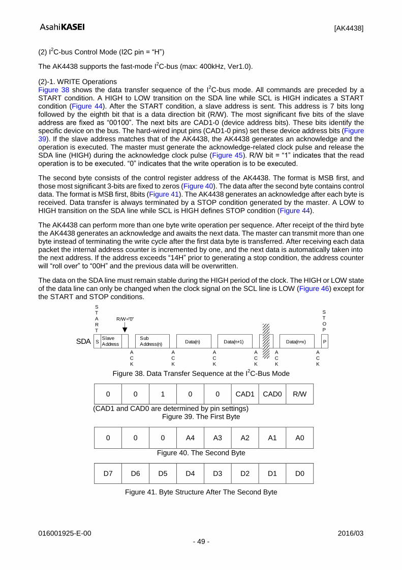
(2) I2C-bus Control Mode (I2C pin = “H”)
The AK4438 supports the fast-mode I2C-bus (max: 400kHz, Ver1.0).
(2)-1. WRITE Operations Figure 38 shows the data transfer sequence of the I
2C-bus mode. All commands are preceded by a
START condition. A HIGH to LOW transition on the SDA line while SCL is HIGH indicates a START condition (Figure 44). After the START condition, a slave address is sent. This address is 7 bits long followed by the eighth bit that is a data direction bit (R/W). The most significant five bits of the slave address are fixed as “00100”. The next bits are CAD1-0 (device address bits). These bits identify the specific device on the bus. The hard-wired input pins (CAD1-0 pins) set these device address bits (Figure 39). If the slave address matches that of the AK4438, the AK4438 generates an acknowledge and the operation is executed. The master must generate the acknowledge-related clock pulse and release the SDA line (HIGH) during the acknowledge clock pulse (Figure 45). R/W bit = “1” indicates that the read operation is to be executed. “0” indicates that the write operation is to be executed.
The second byte consists of the control register address of the AK4438. The format is MSB first, and those most significant 3-bits are fixed to zeros (Figure 40). The data after the second byte contains control data. The format is MSB first, 8bits (Figure 41). The AK4438 generates an acknowledge after each byte is received. Data transfer is always terminated by a STOP condition generated by the master. A LOW to HIGH transition on the SDA line while SCL is HIGH defines STOP condition (Figure 44).
The AK4438 can perform more than one byte write operation per sequence. After receipt of the third byte the AK4438 generates an acknowledge and awaits the next data. The master can transmit more than one byte instead of terminating the write cycle after the first data byte is transferred. After receiving each data packet the internal address counter is incremented by one, and the next data is automatically taken into the next address. If the address exceeds “14H” prior to generating a stop condition, the address counter will “roll over” to “00H” and the previous data will be overwritten.
The data on the SDA line must remain stable during the HIGH period of the clock. The HIGH or LOW state of the data line can only be changed when the clock signal on the SCL line is LOW (Figure 46) except for the START and STOP conditions.
SDASlave
AddressS
S
T
A
R
T
R/W="0"
A
C
K
Sub
Address(n)
A
C
K
Data(n)
A
C
K
Data(n+1)
A
C
K
A
C
K
Data(n+x)
A
C
K
P
S
T
O
P
Figure 38. Data Transfer Sequence at the I
2C-Bus Mode
0 0 1 0 0 CAD1 CAD0 R/W
(CAD1 and CAD0 are determined by pin settings) Figure 39. The First Byte
0 0 0 A4 A3 A2 A1 A0
Figure 40. The Second Byte
D7 D6 D5 D4 D3 D2 D1 D0
Figure 41. Byte Structure After The Second Byte

[AK4438]
016001925-E-00 2016/03 - 50 -
(2)-2. READ Operations Set the R/W bit = “1” for the READ operation of the AK4438. After transmission of data, the master can read the next address’s data by generating an acknowledge instead of terminating the write cycle after the receipt of the first data word. After receiving each data packet the internal address counter is incremented by one, and the next data is automatically taken into the next address. If the address exceeds “14H” prior to generating stop condition, the address counter will “roll over” to “00H” and the data of “00H” will be read out. The AK4438 supports two basic read operations: Current Address Read and Random Address Read. (2)-2-1. Current Address Read The AK4438 contains an internal address counter that maintains the address of the last word accessed, incremented by one. Therefore, if the last access (either a read or write) was to address “n”, the next CURRENT READ operation would access data from the address “n+1”. After receipt of the slave address with R/W bit “1”, the AK4438 generates an acknowledge, transmits 1-byte of data to the address set by the internal address counter and increments the internal address counter by 1. If the master does not generate an acknowledge but generates a stop condition instead, the AK4438 ceases transmission.
SDASlave
AddressS
S
T
A
R
T
R/W="1"
A
C
K
A
C
K
Data(n+1)
A
C
K
Data(n+2)
A
C
K
A
C
K
Data(n+x)
N
A
C
K
P
S
T
O
P
Data(n)
MASTER
MASTER
MASTER
MASTER
MASTER
Figure 42. Current Address Read
(2)-2-2. Random Address Read The random read operation allows the master to access any memory location at random. Prior to issuing a slave address with the R/W bit =“1”, the master must execute a “dummy” write operation first. The master issues a start request, a slave address (R/W bit = “0”) and then the register address to read. After the register address is acknowledged, the master immediately reissues the start request and the slave address with the R/W bit =“1”. The AK4438 then generates an acknowledge, 1 byte of data and increments the internal address counter by 1. If the master does not generate an acknowledge but generates a stop condition instead, the AK4438 ceases transmission.
SDASlave
AddressS
S
T
A
R
T
R/W="0"
A
C
K
A
C
K
A
C
K
Data(n)
A
C
K
Data(n+x)
A
C
K
P
S
T
O
P
Sub
Address(n)S
Slave
Address
R/W="1"
S
T
A
R
T
Data(n+1)
A
C
K
N
A
C
K
MASTER
MASTER
MASTER
MASTER
Figure 43. Random Address Read
[AK4438]
016001925-E-00 2016/03 - 51 -
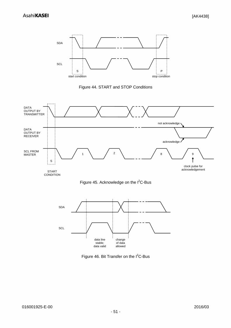
SCL
SDA
stop conditionstart condition
S P
Figure 44. START and STOP Conditions
SCL FROMMASTER
acknowledge
DATAOUTPUT BYTRANSMITTER
DATAOUTPUT BYRECEIVER
1 98
STARTCONDITION
not acknowledge
clock pulse foracknowledgement
S
2
Figure 45. Acknowledge on the I2C-Bus
SCL
SDA
data linestable;
data valid
changeof dataallowed
Figure 46. Bit Transfer on the I2C-Bus

[AK4438]
016001925-E-00 2016/03 - 52 -
■ Register Map
Addr Register Name D7 D6 D5 D4 D3 D2 D1 D0
00H Control 1 ACKS 0 0 0 DIF2 DIF1 DIF0 RSTN
01H Control 2 0 0 SD DFS1 DFS0 DEM11 DEM10 SMUTE
02H Control 3 0 0 0 0 MONO1 DZFB SELLR1 SLOW
03H L1ch ATT ATT7 ATT6 ATT5 ATT4 ATT3 ATT2 ATT1 ATT0
04H R1ch ATT ATT7 ATT6 ATT5 ATT4 ATT3 ATT2 ATT1 ATT0
05H Control 4 INVL1 INVR1 INVL2 INVR2 SELLR2 0 DFS2 SSLOW
06H - 0 0 0 0 0 0 0 0
07H Control 6 L3 R3 L4 R4 0 0 0 SYNCE
08H Control 7 L1 R1 L2 R2 0 0 0 0
09H - 0 0 0 0 0 0 0 0
0AH Control 8 TDM1 TDM0 SDS1 SDS2 PW2 PW1 DEM21 DEM20
0BH Control 9 ATS1 ATS0 0 SDS0 PW4 PW3 0 0
0CH Control 10 INVR4 INVL4 INVR3 INVL3 0 0 0 0
0DH Control 11 MONO4 MONO3 MONO2 0 SELLR4 SELLR3 0 0
0EH Control 12 DEM41 DEM40 DEM31 DEM30 0 0 0 0
0FH L2ch ATT ATT7 ATT6 ATT5 ATT4 ATT3 ATT2 ATT1 ATT0
10H R2ch ATT ATT7 ATT6 ATT5 ATT4 ATT3 ATT2 ATT1 ATT0
11H L3ch ATT ATT7 ATT6 ATT5 ATT4 ATT3 ATT2 ATT1 ATT0
12H R3ch ATT ATT7 ATT6 ATT5 ATT4 ATT3 ATT2 ATT1 ATT0
13H L4ch ATT ATT7 ATT6 ATT5 ATT4 ATT3 ATT2 ATT1 ATT0
14H R4ch ATT ATT7 ATT6 ATT5 ATT4 ATT3 ATT2 ATT1 ATT0
Notes: Data must not be written into addresses from 15H to 1FH.
The bit defined as 0 must contain a “0” value. When the PDN pin goes to “L”, the registers are initialized to their default values. When RSTN bit goes to “0”, the internal timing is reset, but registers are not initialized.
[AK4438]
016001925-E-00 2016/03 - 53 -
■ Register Definitions
Addr Register Name D7 D6 D5 D4 D3 D2 D1 D0
00H Control 1 ACKS 0 0 0 DIF2 DIF1 DIF0 RSTN
R/W R/W R/W R/W R/W R/W R/W R/W R/W
Default 0 0 0 0 1 1 0 1
RSTN: Internal Timing Reset
0: Reset The DZF pin goes “H” but register values are not initialized. 1: Normal Operation (default)
DIF2-0: Audio Data Interface Modes (Table 9) Default value is “110” (Mode 6: 32-bit MSB justified).
ACKS: Master Clock Frequency Auto Setting Mode Enable
0: Disable, Manual Setting Mode (default) 1: Enable, Auto Setting Mode When ACKS bit = “1”, the MCLK frequency is detected automatically.
Addr Register Name D7 D6 D5 D4 D3 D2 D1 D0
01H Control 2 0 0 SD DFS1 DFS0 DEM11 DEM10 SMUTE
R/W R/W R/W R/W R/W R/W R/W R/W R/W
Default 0 0 1 0 0 0 1 0
SMUTE: Soft Mute Enable. 0: Normal Operation (default) 1: DAC outputs soft-muted.
DEM11-0: DAC1 De-emphasis Response (Table 8) Default value is “01” (OFF).
DFS2-0: Sampling Speed Control (Table 1)
Default value is “000” (Normal Speed). A click noise occurs when switching DFS2-0 bits setting.
SD: Short delay Filter Enable. (Table 11)
0: Sharp roll off filter or Slow roll off filter 1: Short delay Sharp roll off filter or Short delay Slow roll off filter (default)

[AK4438]
016001925-E-00 2016/03 - 54 -
Addr Register Name D7 D6 D5 D4 D3 D2 D1 D0
02H Control 3 0 0 0 0 MONO1 DZFB SELLR1 SLOW
R/W R/W R/W R/W R/W R/W R/W R/W R/W
Default 0 0 0 0 0 0 0 0
SLOW: Slow Roll-off Filter Enable (Table 11)
0: Sharp Roll-off Filter (default) 1: Slow Roll-off Filter
SELLR1: The data selection of DAC1 (Table 15) Default value is “0”
DZB: Inverting Enable of DZF (Table 12) 0: DZF pin goes “H” at Zero Detection (default) 1: DZF pin goes “L” at Zero Detection
MONO1: DAC1 enters monaural output mode when MONO bit = “1” (Table 15). 0: Stereo mode (default) 1: MONO mode
Addr Register Name D7 D6 D5 D4 D3 D2 D1 D0
03H L1ch ATT ATT7 ATT6 ATT5 ATT4 ATT3 ATT2 ATT1 ATT0
04H R1ch ATT ATT7 ATT6 ATT5 ATT4 ATT3 ATT2 ATT1 ATT0
R/W R/W R/W R/W R/W R/W R/W R/W R/W
Default 1 1 1 1 1 1 1 1
ATT7-0: Attenuation Level (Table 13)
Default value is “FF” (0dB)
Addr Register Name D7 D6 D5 D4 D3 D2 D1 D0
05H Control 4 INVL1 INVR1 INVL2 INVR2 SELLR2 0 DFS2 SSLOW
R/W R/W R/W R/W R/W R/W R/W R/W R/W
Default 0 0 0 0 0 0 0 0
SSLOW: Digital Filter bypass mode Enable (Table 11)
0: Disable (default) 1: Enable
DFS2-0: Sampling Speed Control (Table 1) Default value is “000” (Normal Speed).
A click noise occurs when switching DFS2-0 bits setting.
SELLR2: The data selection of DAC2 (Table 16) Default value is “0”
INVL1: AOUTL1 Output Phase Inverting Bit (Table 15) INVR1: AOUTR1 Output Phase Inverting Bit (Table 15) INVL2: AOUTL2 Output Phase Inverting Bit (Table 16) INVR2: AOUTR2 Output Phase Inverting Bit (Table 16)
0: Normal (default) 1: Inverted

[AK4438]
016001925-E-00 2016/03 - 55 -
Addr Register Name D7 D6 D5 D4 D3 D2 D1 D0
07H Control 6 L3 R3 L4 R4 0 0 0 SYNCE
R/W R/W R/W R/W R/W R/W R/W R/W R/W
Default 0 0 0 0 0 0 0 1
SYNCE: SYNC Mode Enable
0: SYNC Mode Disable 1: SYNC Mode Enable (default)
L3-4, R3-4: Zero Detect Flag Enable Bit for the DZF pin
0: Disable(default) 1: Enable
Addr Register Name D7 D6 D5 D4 D3 D2 D1 D0
08H Control 7 L1 R1 L2 R2 0 0 0 0
R/W R/W R/W RD RD R/W R/W R/W R/W
Default 0 0 0 0 0 0 0 0
L1-2, R1-2: Zero Detect Flag Enable Bit for the DZF pin
0: Disable(default) 1: Enable
Addr Register Name D7 D6 D5 D4 D3 D2 D1 D0
0AH Control 8 TDM1 TDM0 SDS1 SDS2 PW2 PW1 DEM21 DEM20
R/W R/W R/W R/W R/W R/W R/W R/W R/W
Default 0 0 0 0 1 1 0 1
DEM21-20: DAC2 De-emphasis Response (Table 8)
Default value is “01”. (OFF)
PW2-1: Power Down control for DAC PW2: Power management for DAC2 0: DAC2 power OFF 1: DAC2 power ON (default) PW1: Power management for DAC1 0: DAC1 power OFF 1: DAC1 power ON (default)
SDS2-0: DAC1-4 Data Select
0: Normal Operation 1: Output Other Slot Data (Table 10) Default value is “000”.
TDM1-0: TDM Mode Select (Table 9)
Default value is “00”.

[AK4438]
016001925-E-00 2016/03 - 56 -
Addr Register Name D7 D6 D5 D4 D3 D2 D1 D0
0BH Control 9 ATS1 ATS0 0 SDS0 PW4 PW3 0 0
R/W R/W R/W R/W R/W R/W R/W R/W R/W
Default 0 0 0 0 1 1 0 0
PW4-3: Power Down control for DAC
PW4: Power management for DAC4 0: DAC4 power OFF 1: DAC4 power ON (default) PW3: Power management for DAC3 0: DAC3 power OFF 1: DAC3 power ON (default)
SDS2-0: DAC1-4 Data Select
0: Normal Operation 1: Output Other Slot Data (Table 10) The default value is “000”.
ATS1-0: Transition Time between Set Values of ATT7-0 bits (Table 14)
The default value is “00”.
Addr Register Name D7 D6 D5 D4 D3 D2 D1 D0
0CH Control 6 INVR4 INVL4 INVR3 INVL3 0 0 0 0
R/W R/W R/W R/W R/W R/W R/W R/W R/W
Default 0 0 0 0 0 0 0 0
INVL3: AOUTL3 Output Phase Inverting Bit (Table 17) INVR3: AOUTR3 Output Phase Inverting Bit (Table 17) INVL4: AOUTL4 Output Phase Inverting Bit (Table 18) INVR4: AOUTR4 Output Phase Inverting Bit (Table 18)
0: Normal (default) 1: Inverted
Addr Register Name D7 D6 D5 D4 D3 D2 D1 D0
0DH Control 6 MONO4 MONO3 MONO2 0 SELLR4 SELLR3 0 0
R/W R/W R/W R/W R/W R/W R/W R/W R/W
Default 0 0 0 0 0 0 0 0
SELLR3: The data selection of DAC3 (Table 17) SELLR4: The data selection of DAC4 (Table 18)
The default value is “0”.
MONO2: DAC2 enters Mono output mode when MONO2 bit =“1”. (Table 16) MONO3: DAC3 enters Mono output mode when MONO3 bit =“1”. (Table 17) MONO4: DAC4 enters Mono output mode when MONO4 bit =“1”. (Table 18)
0: Stereo mode (default) 1: MONO mode

[AK4438]
016001925-E-00 2016/03 - 57 -
Addr Register Name D7 D6 D5 D4 D3 D2 D1 D0
0EH Control 6 DEM41 DEM40 DEM31 DEM30 0 0 0 0
R/W R/W R/W R/W R/W R/W R/W R/W R/W
Default 0 1 0 1 0 0 0 0
DEM31-30: DAC3 De-emphasis Response (Table 8) DEM41-40: DAC4 De-emphasis Response (Table 8)
The default value is “01”, OFF
Addr Register Name D7 D6 D5 D4 D3 D2 D1 D0
0FH L2ch ATT ATT7 ATT6 ATT5 ATT4 ATT3 ATT2 ATT1 ATT0
10H R2ch ATT ATT7 ATT6 ATT5 ATT4 ATT3 ATT2 ATT1 ATT0
11H L3ch ATT ATT7 ATT6 ATT5 ATT4 ATT3 ATT2 ATT1 ATT0
12H R3ch ATT ATT7 ATT6 ATT5 ATT4 ATT3 ATT2 ATT1 ATT0
13H L4ch ATT ATT7 ATT6 ATT5 ATT4 ATT3 ATT2 ATT1 ATT0
14H R4ch ATT ATT7 ATT6 ATT5 ATT4 ATT3 ATT2 ATT1 ATT0
R/W R/W R/W R/W R/W R/W R/W R/W R/W
Default 1 1 1 1 1 1 1 1
ATT7-0: Attenuation Level (Table 13) The default value is “FF”, (0dB)

[AK4438]
016001925-E-00 2016/03 - 58 -
13. Recommended External Circuits
■ Typical Connection Diagram
DSP
P Power Supply
1.7 3.6V
AOUTR3
AOUTL4
AOUTR4
TEST
I2C
TVDD
VSS1
AO
UT
L3
AV
DD
V
SS
2
V
CO
M
VR
EF
L
AO
UT
L2
BIC
K
LR
CK
SD
TI1
SD
TI2
SD
TI3
SD
TI4
DZ
F
AOUTR1
AOUTL1
PS/CAD0_SPI
CAD0_I2C/CSN/DIF
SCL/CCLK/TDM1
SDA/CDTI/TDM0
SMUTE/CAD1
PDN
AK4438
Top View
25
26
27
28
29
30
31
24
23
16
15
14
13
12
11
10
9
22
21
20
19
18
1
2
3
4
5
6
7
8
32
17
VR
EF
H
A
OU
TR
2
LDOO
Power Supply
3.0 3.6V
2.2u
MC
LK
+
0.1u
10u
+ 10u 0.1u
2.2u
H : I2C L : SPI
L1
ch o
ut
R1
ch
ou
t
L2
ch o
ut
R2
ch
ou
t
L3
ch o
ut
R3
ch
ou
t
L4
ch o
ut
R4
ch
ou
t
+
0.1u
10u
Analog Ground Digital Ground
Analog Ground
Digital Ground
Figure 47. Typical Connection Diagram
Note: The AK4438 integrates smoothing filters.

[AK4438]
016001925-E-00 2016/03 - 59 -
1. Grounding and Power Supply Decoupling The AK4438 requires careful attention to power supply and grounding arrangements. AVDD and TVDD are usually supplied from the analog supply of the system. If AVDD and TVDD are supplied separately, the power-up sequences between AVDD and TVDD is not critical. VSS1 and VSS2 must be connected to the same analog ground plane. System analog ground and digital ground should be wired separately and connected together as close as possible to where the supplies are brought onto the printed circuit board. Decoupling capacitors should be as near to the AK4438 as possible.
2. Voltage Reference The differential voltage between VREFH pin and VREFL pin sets the analog output range. The VREFH pin is normally connected to AVDD, and the VREFL pin is normally connected to VSS2. VREFHL and VREFL should be connected with a 0.1µF ceramic capacitor and 10µF electrolytic capacitor as near as possible to the pin to eliminate the effects of high frequency noise.
VCOM is a signal ground of this chip and output the voltage AVDDx1/2. A 2.2F ±50% ceramic capacitor attached between the VCOM pin and VSS2 eliminates the effects of high frequency noise. This capacitor should be as close to the pin as possible. No load current may be drawn from the VCOM pin. All signals, especially clocks, should be kept away from the VREFH pin and the VCOM pin in order to avoid unwanted coupling into the AK4438. LDOO outputs 1.2V that is used for internal digital circuit. LDOO and VSS1 should be connected with a
2.2F ±50% ceramic capacitor as near as possible to the pin to stabilize internal LDO. No load current may be drawn from the VCOM pin.
3. Analog Output The output signal range is nominally 0.86 x VREFH Vpp centered around the VCOM voltage. The DAC input data format is 2’s complement. The output voltage is a positive full scale for 7FFFFFFFH (@32bit) and a negative full scale for 80000000H (@32bit). The ideal output is VCOM voltage for 00000000H (@32bit). The internal analog filters remove most of the noise generated by the delta-sigma modulator of DAC beyond the audio passband, in single-ended input mode. Normally, DC component is cut by an external capacitor since the DAC outputs have DC offsets of a few millivolts to the VCOM voltage.
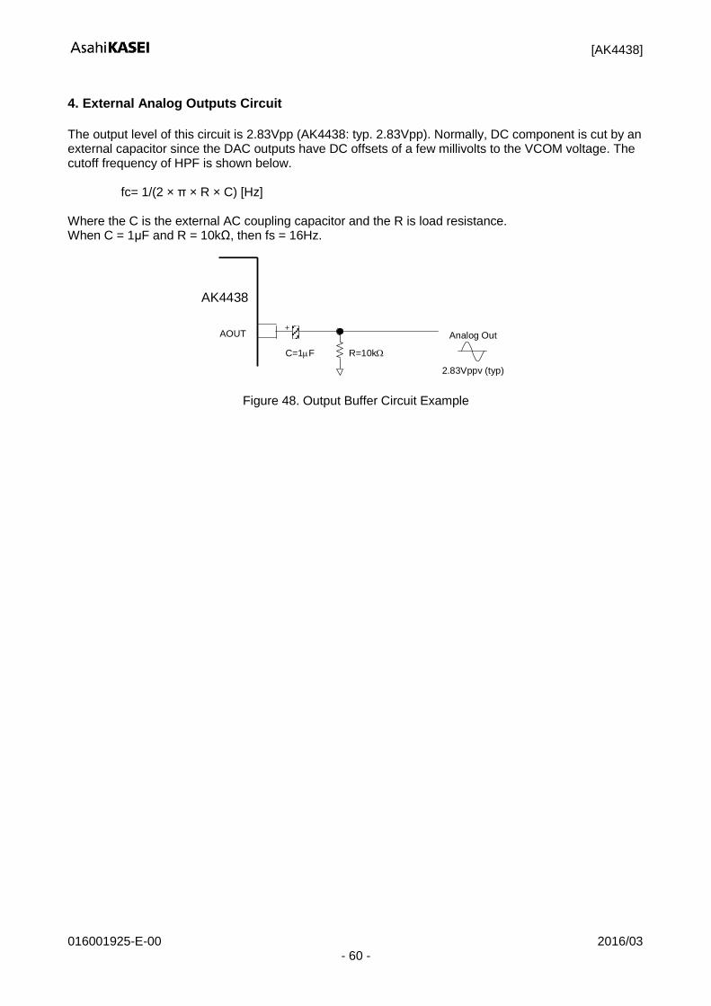
[AK4438]
016001925-E-00 2016/03 - 60 -
4. External Analog Outputs Circuit The output level of this circuit is 2.83Vpp (AK4438: typ. 2.83Vpp). Normally, DC component is cut by an external capacitor since the DAC outputs have DC offsets of a few millivolts to the VCOM voltage. The cutoff frequency of HPF is shown below.
fc= 1/(2 × π × R × C) [Hz] Where the C is the external AC coupling capacitor and the R is load resistance. When C = 1μF and R = 10kΩ, then fs = 16Hz.
AK4438
AOUT Analog Out
R=10k
2.83Vppv (typ)
C=1F
Figure 48. Output Buffer Circuit Example

[AK4438]
016001925-E-00 2016/03 - 61 -
14. Package
■ Outline Dimensions
32-pin QFN (Unit: mm)
■ Material & Lead Finish
Package molding compound: Epoxy, Halogen (Br and Cl) free Lead frame material: Cu Terminal surface treatment: Solder (Pb free) plate
[AK4438]
016001925-E-00 2016/03 - 62 -
■ Marking
4438
XXXX
1
1) Pin #1 indication 2) Date Code: XXXX (4 digits) 3) Marking Code: 4438
15. Ordering Guide
■ Ordering Guide
AK4438VN -40 +105C 32-pin QFN (0.5mm pitch) AKD4438 Evaluation Board for the AK4438
16. Revision History
Date (Y/M/D) Revision Reason Page Contents
16/03/04 00 First Edition

[AK4438]
016001925-E-00 2016/03 - 63 -
IMPORTANT NOTICE
0. Asahi Kasei Microdevices Corporation (“AKM”) reserves the right to make changes to the
information contained in this document without notice. When you consider any use or application of AKM product stipulated in this document (“Product”), please make inquiries the sales office of AKM or authorized distributors as to current status of the Products.
1. All information included in this document are provided only to illustrate the operation and application examples of AKM Products. AKM neither makes warranties or representations with respect to the accuracy or completeness of the information contained in this document nor grants any license to any intellectual property rights or any other rights of AKM or any third party with respect to the information in this document. You are fully responsible for use of such information contained in this document in your product design or applications. AKM ASSUMES NO LIABILITY FOR ANY LOSSES INCURRED BY YOU OR THIRD PARTIES ARISING FROM THE USE OF SUCH INFORMATION IN YOUR PRODUCT DESIGN OR APPLICATIONS.
2. The Product is neither intended nor warranted for use in equipment or systems that require extraordinarily high levels of quality and/or reliability and/or a malfunction or failure of which may cause loss of human life, bodily injury, serious property damage or serious public impact, including but not limited to, equipment used in nuclear facilities, equipment used in the aerospace industry, medical equipment, equipment used for automobiles, trains, ships and other transportation, traffic signaling equipment, equipment used to control combustions or explosions, safety devices, elevators and escalators, devices related to electric power, and equipment used in finance-related fields. Do not use Product for the above use unless specifically agreed by AKM in writing.
3. Though AKM works continually to improve the Product’s quality and reliability, you are responsible for complying with safety standards and for providing adequate designs and safeguards for your hardware, software and systems which minimize risk and avoid situations in which a malfunction or failure of the Product could cause loss of human life, bodily injury or damage to property, including data loss or corruption.
4. Do not use or otherwise make available the Product or related technology or any information contained in this document for any military purposes, including without limitation, for the design, development, use, stockpiling or manufacturing of nuclear, chemical, or biological weapons or missile technology products (mass destruction weapons). When exporting the Products or related technology or any information contained in this document, you should comply with the applicable export control laws and regulations and follow the procedures required by such laws and regulations. The Products and related technology may not be used for or incorporated into any products or systems whose manufacture, use, or sale is prohibited under any applicable domestic or foreign laws or regulations.
5. Please contact AKM sales representative for details as to environmental matters such as the RoHS compatibility of the Product. Please use the Product in compliance with all applicable laws and regulations that regulate the inclusion or use of controlled substances, including without limitation, the EU RoHS Directive. AKM assumes no liability for damages or losses occurring as a result of noncompliance with applicable laws and regulations.
6. Resale of the Product with provisions different from the statement and/or technical features set forth in this document shall immediately void any warranty granted by AKM for the Product and shall not create or extend in any manner whatsoever, any liability of AKM.
7. This document may not be reproduced or duplicated, in any form, in whole or in part, without prior written consent of AKM.


![115dB 768kHz 32-bit 2ch Premium DAC - AKM€¦ · TST2 SS P N V 1 Back Tab:Note1 Note 1. The exposed pad at back face of the package must be open or connected to the ground. [AK4452]](https://static.documents.pub/doc/80x56/5fe159cfb0acf0679a4da857/115db-768khz-32-bit-2ch-premium-dac-akm-tst2-ss-p-n-v-1-back-tabnote1-note-1.jpg)
