
TS-S08D011D October, 2010
SPP5100 Series Sumitomo Electric Industries, Ltd. Page 1
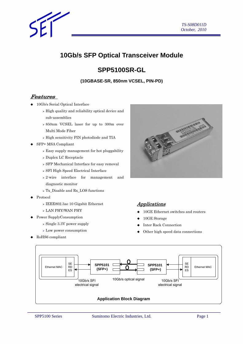
10Gb/s SFP Optical Transceiver Module
SPP5100SR-GL (10GBASE-SR, 850nm VCSEL, PIN-PD)
Features
10Gb/s Serial Optical Interface
High quality and reliability optical device and
sub-assemblies
850nm VCSEL laser for up to 300m over
Multi Mode Fiber
High sensitivity PIN photodiode and TIA
SFP+ MSA Compliant
Easy supply management for hot pluggability
Duplex LC Receptacle
SFP Mechanical Interface for easy removal
SFI High Speed Electrical Interface
2-wire interface for management and
diagnostic monitor
Tx_Disable and Rx_LOS functions
Protocol
IEEE802.3ae 10 Gigabit Ethernet
LAN PHY/WAN PHY
Power SupplyConsumption
Single 3.3V power supply
Low power consumption
RoHS6 compliant
Applications 10GE Ethernet switches and routers
10GE Storage
Inter Rack Connection
Other high speed data connections
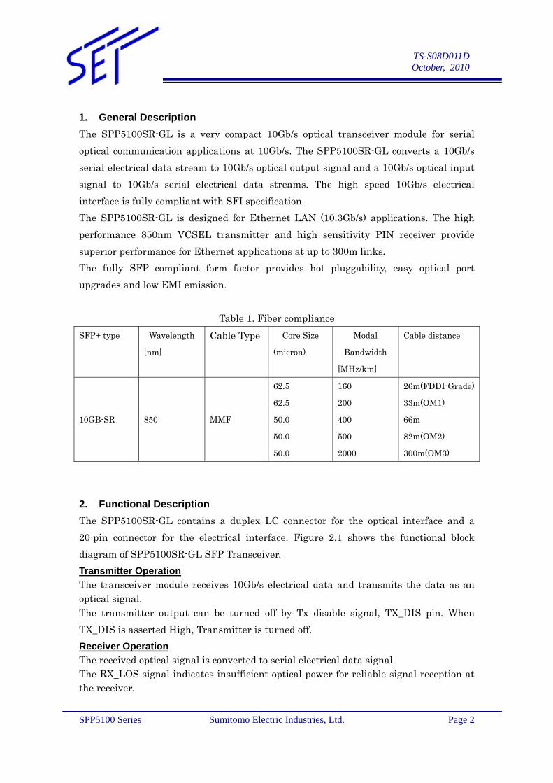
SPP5101 (SFP+)
SERDES
Ethernet MAC SPP5101 (SFP+)
SERDES
Ethernet MAC
Application Block Diagram
10Gb/s optical signal10Gb/s SFIelectrical signal
10Gb/s SFIelectrical signal
TS-S08D011D October, 2010
SPP5100 Series Sumitomo Electric Industries, Ltd. Page 2
1. General Description The SPP5100SR-GL is a very compact 10Gb/s optical transceiver module for serial optical communication applications at 10Gb/s. The SPP5100SR-GL converts a 10Gb/s serial electrical data stream to 10Gb/s optical output signal and a 10Gb/s optical input signal to 10Gb/s serial electrical data streams. The high speed 10Gb/s electrical interface is fully compliant with SFI specification. The SPP5100SR-GL is designed for Ethernet LAN (10.3Gb/s) applications. The high performance 850nm VCSEL transmitter and high sensitivity PIN receiver provide superior performance for Ethernet applications at up to 300m links. The fully SFP compliant form factor provides hot pluggability, easy optical port upgrades and low EMI emission.
Table 1. Fiber compliance SFP+ type Wavelength
[nm]
Cable Type Core Size
(micron)
Modal
Bandwidth
[MHz/km]
Cable distance
10GB-SR 850 MMF
62.5
62.5
50.0
50.0
50.0
160
200
400
500
2000
26m(FDDI-Grade)
33m(OM1)
66m
82m(OM2)
300m(OM3)
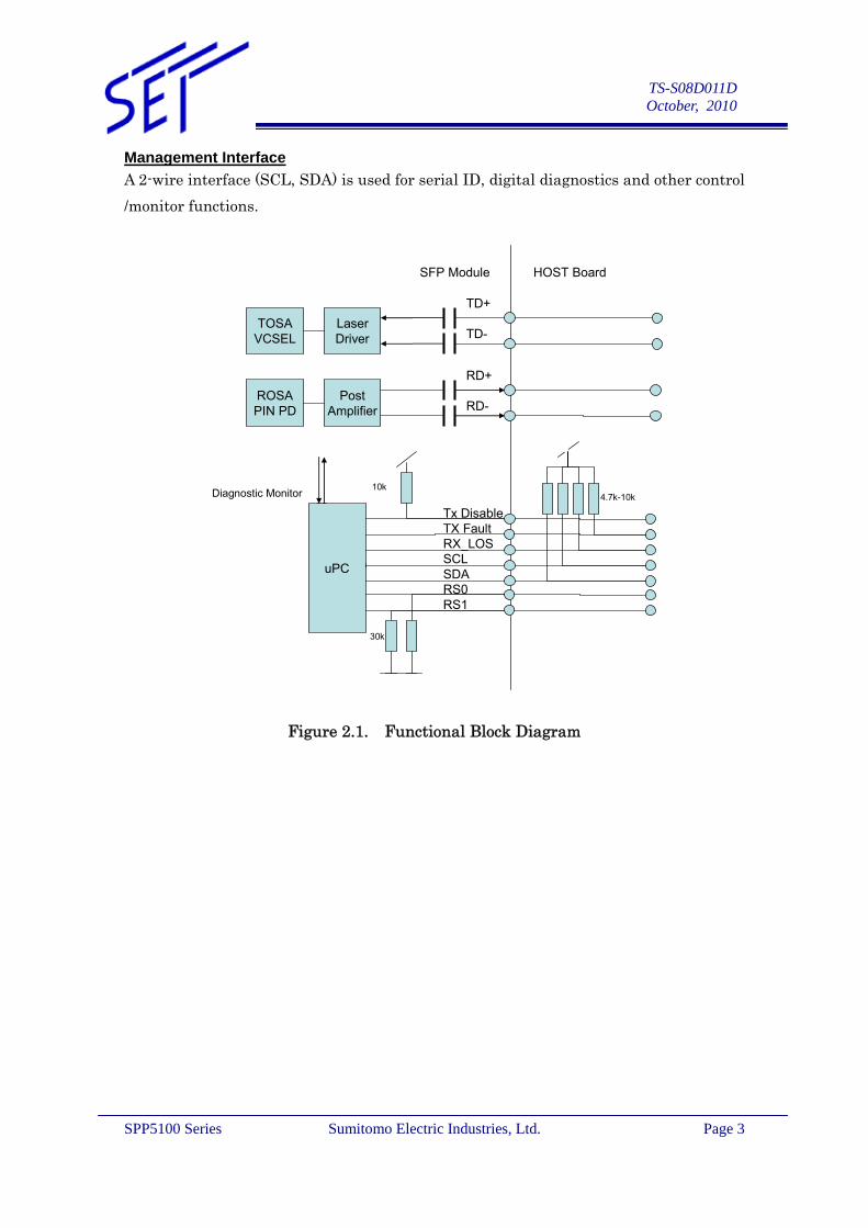
2. Functional Description The SPP5100SR-GL contains a duplex LC connector for the optical interface and a 20-pin connector for the electrical interface. Figure 2.1 shows the functional block diagram of SPP5100SR-GL SFP Transceiver. Transmitter Operation The transceiver module receives 10Gb/s electrical data and transmits the data as an optical signal. The transmitter output can be turned off by Tx disable signal, TX_DIS pin. When TX_DIS is asserted High, Transmitter is turned off. Receiver Operation The received optical signal is converted to serial electrical data signal. The RX_LOS signal indicates insufficient optical power for reliable signal reception at the receiver.
TS-S08D011D October, 2010
SPP5100 Series Sumitomo Electric Industries, Ltd. Page 3
Management Interface A 2-wire interface (SCL, SDA) is used for serial ID, digital diagnostics and other control /monitor functions.
LaserDriver
PostAmplifier
Diagnostic Monitor
TOSAVCSEL
ROSAPIN PD
Tx DisableTX FaultRX_LOSSCLSDARS0RS1
TD+
TD-
RD+
RD-
30k
10k
uPC
4.7k-10k
SFP Module HOST Board
Figure 2.1. Functional Block Diagram
TS-S08D011D October, 2010
SPP5100 Series Sumitomo Electric Industries, Ltd. Page 4
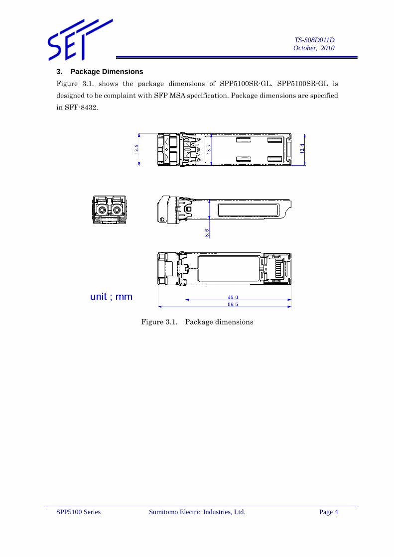
3. Package Dimensions Figure 3.1. shows the package dimensions of SPP5100SR-GL. SPP5100SR-GL is designed to be complaint with SFP MSA specification. Package dimensions are specified in SFF-8432.
Figure 3.1. Package dimensions
TS-S08D011D October, 2010
SPP5100 Series Sumitomo Electric Industries, Ltd. Page 5
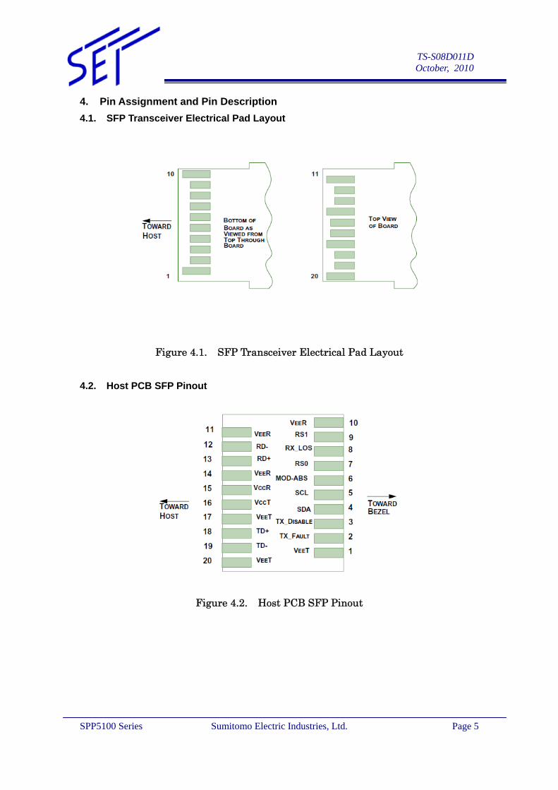
4. Pin Assignment and Pin Description 4.1. SFP Transceiver Electrical Pad Layout
Figure 4.1. SFP Transceiver Electrical Pad Layout 4.2. Host PCB SFP Pinout
Figure 4.2. Host PCB SFP Pinout

TS-S08D011D October, 2010
SPP5100 Series Sumitomo Electric Industries, Ltd. Page 6
4.3. Pin Descriptions Table 4.3. Pin Description
Pin# Name Logic Description
Power
Sequence
Order
Note
1 VeeT Module Transmitter Ground 1st 1
2 Tx_Fault LVTTL-O Module Transmitter Fault 3rd 2
3 Tx_Disable LVTTL-I Transmitter Disable,Turns off transmitter laser
output
3rd 3
4 SDA LVTTL-I/O 2 Wire Serial Interface Data Line(Same as
MOD-DEF2 as defined in the INF-8074i)
3rd
5 SCL LVTTL-I/O 2 Wire Serial Interface Data Line(Same as
MOD-DEF1 as defined in the INF-8074i)
3rd
6 MOD_ABS Module Absent, connected to VeeT or VeeR in the
module
3rd 2
7 RS0 LVTTL-I Rate Select 0 (not functional for 10GE type) 3rd
8 RX_LOS LVTTL-O Receiver Loss of Signal Indication 3rd 2
9 RS1 LVTTL-I Rate Select 1 (not functional for 10GE type) 3rd
10 VeeR Module Receiver Ground 1st 1
11 VeeR Module Receiver Ground 1st 1
12 RD- CML-O Receiver Inverted Data Output 3rd
13 RD+ CML-O Receiver Non-Inverted Data Output 3rd
14 VeeR Module Receiver Ground 1st 1
15 VccR Module Receiver 3.3V Supply 2nd
16 VccT Module Transmitter 3.3V Supply 2nd
17 VeeT Module Transmitter Ground 1st 1
18 TD+ CML-I Transmitter Non-Inverted Data Input 3rd
19 TD- CML-I Transmitter Inverted Data Input 3rd
20 VeeT Module Transmitter Ground 1st 1
Note
1: Module ground pins are isolated from the module case and chassis ground within the module.
2: Shall be pulled up with 4.7k to 10k ohm to a voltage between 3.15V and 3.45V on the host board.
3: Shall be pulled up with 4.7k to 10k ohm to VccT in the module.
TS-S08D011D October, 2010
SPP5100 Series Sumitomo Electric Industries, Ltd. Page 7
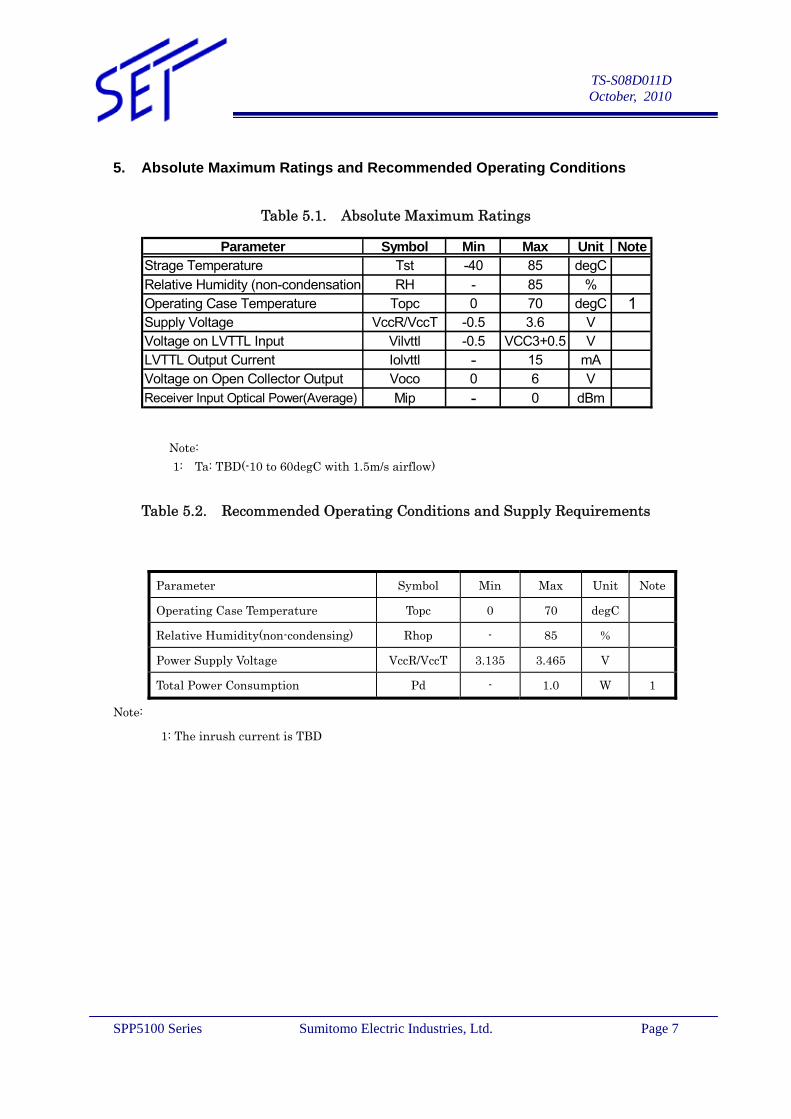
5. Absolute Maximum Ratings and Recommended Operating Conditions
Table 5.1. Absolute Maximum Ratings
Parameter Symbol Min Max Unit NoteStrage Temperature Tst -40 85 degCRelative Humidity (non-condensation) RH - 85 %Operating Case Temperature Topc 0 70 degC 1Supply Voltage VccR/VccT -0.5 3.6 VVoltage on LVTTL Input Vilvttl -0.5 VCC3+0.5 VLVTTL Output Current Iolvttl - 15 mAVoltage on Open Collector Output Voco 0 6 VReceiver Input Optical Power(Average) Mip - 0 dBm
Note: 1: Ta: TBD(-10 to 60degC with 1.5m/s airflow)
Table 5.2. Recommended Operating Conditions and Supply Requirements
Parameter Symbol Min Max Unit Note
Operating Case Temperature Topc 0 70 degC
Relative Humidity(non-condensing) Rhop - 85 %
Power Supply Voltage VccR/VccT 3.135 3.465 V
Total Power Consumption Pd - 1.0 W 1
Note:
1: The inrush current is TBD
TS-S08D011D October, 2010
SPP5100 Series Sumitomo Electric Industries, Ltd. Page 8
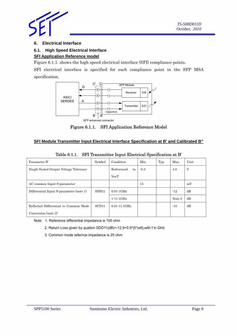
6. Electrical Interface 6.1. High Speed Electrical Interface SFI Application Reference model Figure 6.1.1. shows the high speed electrical interface (SFI) compliance points. SFI electrical interface is specified for each compliance point in the SFP MSA specification.
Figure 6.1.1. SFI Application Reference Model SFI Module Transmitter Input Electrical Interface Specification at B’ and Calibrated B”
Table 6.1.1. SFI Transmitter Input Electrical Specification at B’ Parameter B’ Symbol Condition Min Typ. Max. Unit
Single Ended Output Voltage Tolerance Referenced to
VeeT
-0.3 4.0 V
AC common Input S-parameter 15 mV
0.01-1GHz -12 dB Differential Input S-parameter (note 1) SDD11
1-11.1GHz Note 2 dB
Reflected Differential to Common Mode
Conversion (note 3)
SCD11 0.01-11.1GHz -10 dB
Note 1. Reference differential impedance is 100 ohm
2. Return Loss given by quation SDD11(dB)=-12.9+0.9*(f/1e9),with f in GHz
3. Common mode refernce impedance is 25 ohm
C' C
B' BCapacitors
SFP enhanced connector
D
AASIC/
SERDES
Receiver
Transmitter
O/E
E/O
SFP Module
TS-S08D011D October, 2010
SPP5100 Series Sumitomo Electric Industries, Ltd. Page 9
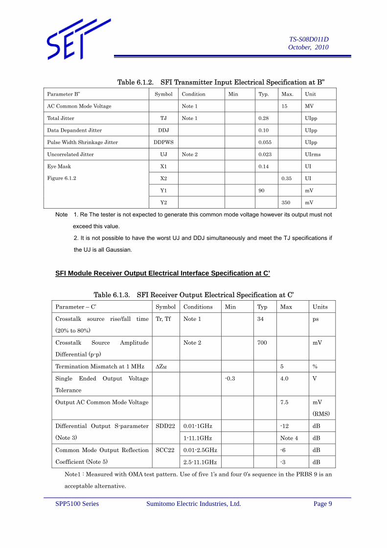
Table 6.1.2. SFI Transmitter Input Electrical Specification at B” Parameter B” Symbol Condition Min Typ. Max. Unit
AC Common Mode Voltage Note 1 15 MV
Total Jitter TJ Note 1 0.28 UIpp
Data Depandent Jitter DDJ 0.10 UIpp
Pulse Width Shrinkage Jitter DDPWS 0.055 UIpp
Uncorrelated Jitter UJ Note 2 0.023 UIrms
X1 0.14 UI
X2 0.35 UI
Y1 90 mV
Eye Mask
Figure 6.1.2
Y2 350 mV
Note 1. Re The tester is not expected to generate this common mode voltage however its output must not
exceed this value.
2. It is not possible to have the worst UJ and DDJ simultaneously and meet the TJ specifications if
the UJ is all Gaussian. SFI Module Receiver Output Electrical Interface Specification at C’
Table 6.1.3. SFI Receiver Output Electrical Specification at C’ Parameter – C’ Symbol Conditions Min Typ Max Units
Crosstalk source rise/fall time
(20% to 80%)
Tr, Tf Note 1 34 ps
Crosstalk Source Amplitude
Differential (p-p)
Note 2 700 mV
Termination Mismatch at 1 MHz ΔZM 5 %
Single Ended Output Voltage
Tolerance
-0.3 4.0 V
Output AC Common Mode Voltage 7.5 mV
(RMS)
0.01-1GHz -12 dB Differential Output S-parameter
(Note 3)
SDD22
1-11.1GHz Note 4 dB
0.01-2.5GHz -6 dB Common Mode Output Reflection
Coefficient (Note 5)
SCC22
2.5-11.1GHz -3 dB
Note1 : Measured with OMA test pattern. Use of five 1’s and four 0’s sequence in the PRBS 9 is an
acceptable alternative.
TS-S08D011D October, 2010
SPP5100 Series Sumitomo Electric Industries, Ltd. Page 10
2 : For dRNx compliance test condition. Crosstalk is not used for dRN.
3 : Refernce differential impedance is 100 ohm.
4 : Dfferntial Output S-parameter given by equation SDD11(dB) = -12.9+0.9*(f/1e9), with f in GHz.
5 : Common mode reference impedance is 25 ohm.
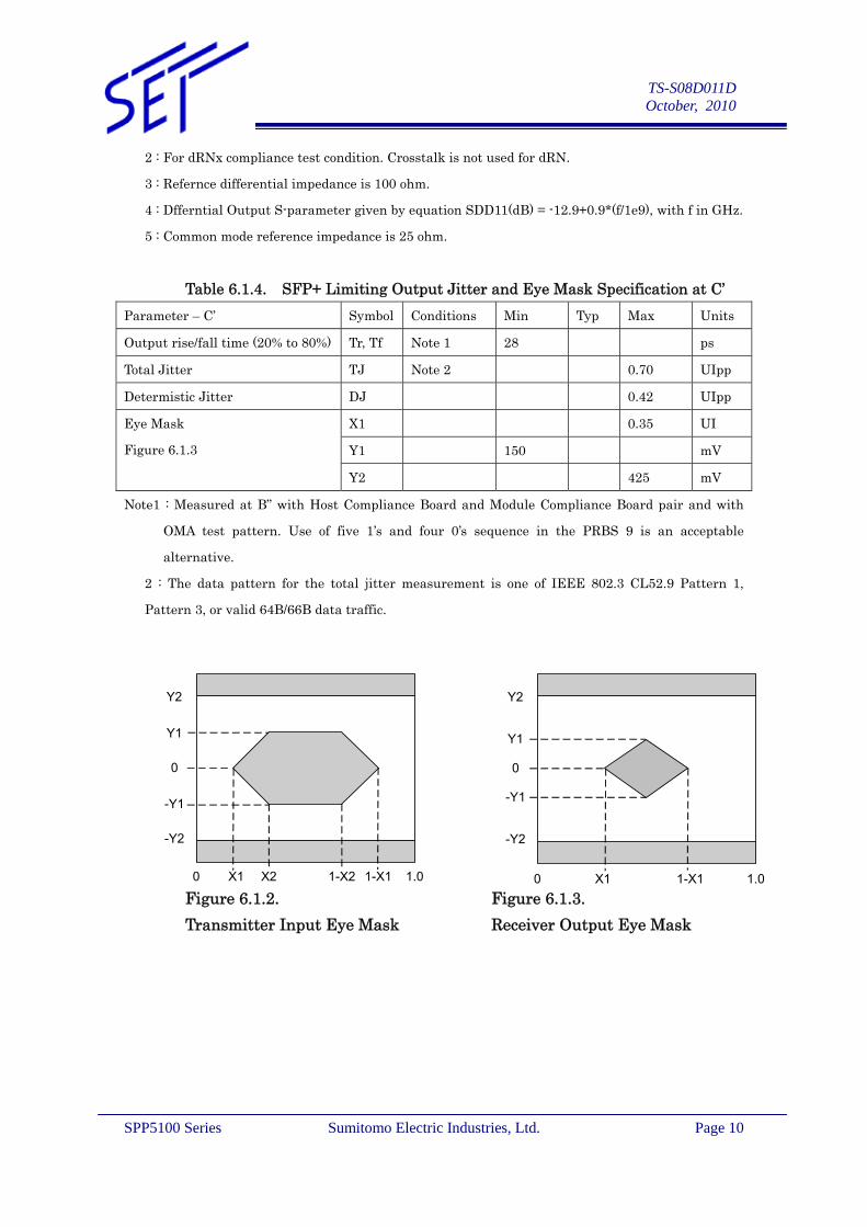
Table 6.1.4. SFP+ Limiting Output Jitter and Eye Mask Specification at C’
Parameter – C’ Symbol Conditions Min Typ Max Units
Output rise/fall time (20% to 80%) Tr, Tf Note 1 28 ps
Total Jitter TJ Note 2 0.70 UIpp
Determistic Jitter DJ 0.42 UIpp
X1 0.35 UI
Y1 150 mV
Eye Mask
Figure 6.1.3
Y2 425 mV
Note1 : Measured at B” with Host Compliance Board and Module Compliance Board pair and with
OMA test pattern. Use of five 1’s and four 0’s sequence in the PRBS 9 is an acceptable
alternative.
2 : The data pattern for the total jitter measurement is one of IEEE 802.3 CL52.9 Pattern 1,
Pattern 3, or valid 64B/66B data traffic. Figure 6.1.2. Figure 6.1.3. Transmitter Input Eye Mask Receiver Output Eye Mask
Y2
-Y2
-Y1
Y1
0
X1 1-X10 1.0X2 1-X20 1.0X1 1-X1
Y2
-Y2
-Y1
Y1
0

TS-S08D011D October, 2010
SPP5100 Series Sumitomo Electric Industries, Ltd. Page 11
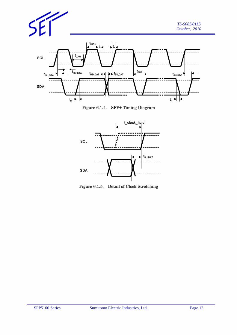
6.2. Low speed Electrical Interface SPP5100SR-GL low speed interface is based on 2-wire interface. Management memory map is based on SFF-8472. 2-wire Electrical Specifications Parameter Symbol Min Max Unit
Host 2-wire Vcc Vcc_host 3.14 3.46 V
VOL 0.0 0.40 V SCL and SDA
VOH Vcc_host-0.5 Vcc_host+0.3 V
VIL -0.3 VccT*0.3 V SCL and SDA
VIH VccT*0.7 VccT+0.5 V
Input current on the SCL and SDA contacts -10 10 uA
Capacitance on SCL and SDA I/O contact 14 pF
2-wire Timing Specifications Parameter Symbol Min Max Unit
Clock Frequency fSCL 0 400 kHz
Clock Pulse Width Low tLOW 1.3 us
Clock Pulse Width High tHIGH 0.6 us
Time bus free before new transmission can
start
tBUF 20 us
START Hold Time tHD, STA 0.6 us
START Set-up Time tSU, STA 0.6 us
Data In Hold Time tHD, DAT 0 us
Data In Set-up Time tSU, DAT 0.1 us
Input Rise Time (100kHz) tR, 100 1000 ns
Input Rise Time (400kHz) tR, 400 300 ns
Input Fall Time (100kHz) tF, 100 300 ns
Input Fall Time (400kHz) tF, 400 300 ns
STOP Set-up Time tSU, STO 0.6 us
Serial Interface Clock Holdoff
“Clock Stretching”
t_clock_hold 500 us
TS-S08D011D October, 2010
SPP5100 Series Sumitomo Electric Industries, Ltd. Page 12
SCL
SDA
tSU,STAtHD,STA
tLOW
tHIGHtF tR
tHD,DAT tSU,DATtBUF
tR
tSU,STO
tF
SCL
SDA
tSU,STAtHD,STA
tLOW
tHIGHtF tR
tHD,DAT tSU,DATtBUF
tR
tSU,STO
tF Figure 6.1.4. SFP+ Timing Diagram
SCL
SDA
t_clock_hold
tSU,DAT
SCL
SDA
t_clock_hold
tSU,DAT
Figure 6.1.5. Detail of Clock Stretching
TS-S08D011D October, 2010
SPP5100 Series Sumitomo Electric Industries, Ltd. Page 13
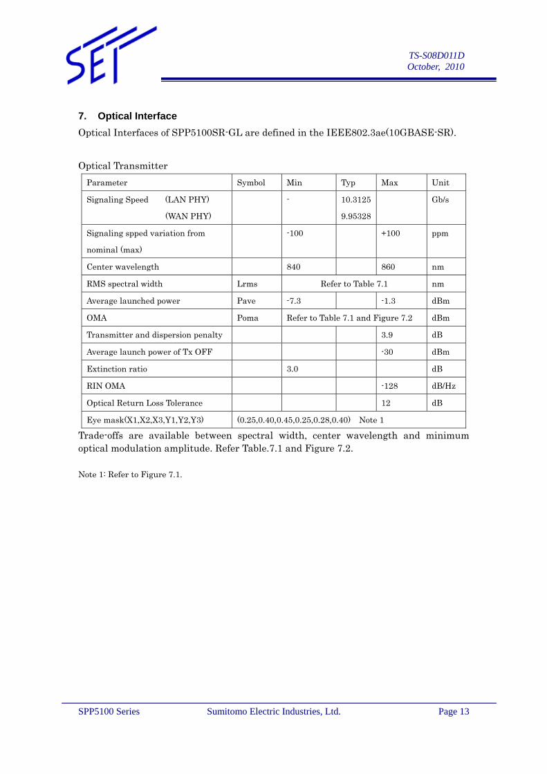
7. Optical Interface Optical Interfaces of SPP5100SR-GL are defined in the IEEE802.3ae(10GBASE-SR). Optical Transmitter
Parameter Symbol Min Typ Max Unit
Signaling Speed (LAN PHY)
(WAN PHY)
- 10.3125
9.95328
Gb/s
Signaling spped variation from
nominal (max)
-100 +100 ppm
Center wavelength 840 860 nm
RMS spectral width Lrms Refer to Table 7.1 nm
Average launched power Pave -7.3 -1.3 dBm
OMA Poma Refer to Table 7.1 and Figure 7.2 dBm
Transmitter and dispersion penalty 3.9 dB
Average launch power of Tx OFF -30 dBm
Extinction ratio 3.0 dB
RIN OMA -128 dB/Hz
Optical Return Loss Tolerance 12 dB
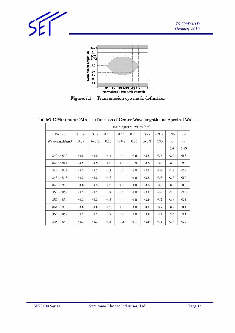
Eye mask(X1,X2,X3,Y1,Y2,Y3) (0.25,0.40,0.45,0.25,0.28,0.40) Note 1
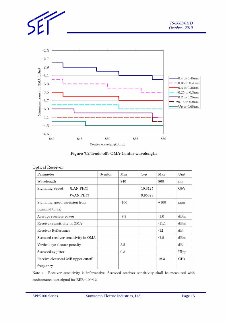
Trade-offs are available between spectral width, center wavelength and minimum optical modulation amplitude. Refer Table.7.1 and Figure 7.2. Note 1: Refer to Figure 7.1.
TS-S08D011D October, 2010
SPP5100 Series Sumitomo Electric Industries, Ltd. Page 14
X1 X2 X3 1-X3 1-X2 1-X10 1
1+Y31
1-Y11-Y2
0.5
Y2Y10
-Y3
Normalized Time (Unit Interval)N
orm
aliz
ed A
mpl
itude
X1 X2 X3 1-X3 1-X2 1-X10 1
1+Y31
1-Y11-Y2
0.5
Y2Y10
-Y3
Normalized Time (Unit Interval)N
orm
aliz
ed A
mpl
itude
Figure.7.1. Transmission eye mask definition
Table7.1: Minimum OMA as a function of Center Wavelenghth and Spectral Width RMS Spectral width (nm)
Center
Wavelength(nm)
Up to
0.05
0.05
to 0.1
0.1 to
0.15
0.15
to 0.2
0.2 to
0.25
0.25
to 0.3
0.3 to
0.35
0.35
to
0.4
0.4
to
0.45
840 to 842 -4.2 -4.2 -4.1 -4.1 -3.9 -3.8 -3.5 -3.2 -2.8
842 to 844 -4.2 -4.2 -4.2 -4.1 -3.9 -3.8 -3.6 -3.3 -2.9
844 to 846 -4.2 -4.2 -4.2 -4.1 -4.0 -3.8 -3.6 -3.3 -2.9
846 to 848 -4.3 -4.2 -4.2 -4.1 -4.0 -3.8 -3.6 -3.3 -2.9
848 to 850 -4.3 -4.2 -4.2 -4.1 -4.0 -3.8 -3.6 -3.3 -3.0
850 to 852 -4.3 -4.2 -4.2 -4.1 -4.0 -3.8 -3.6 -3.4 -3.0
852 to 854 -4.3 -4.2 -4.2 -4.1 -4.0 -3.9 -3.7 -3.4 -3.1
854 to 856 -4.3 -4.3 -4.2 -4.1 -4.0 -3.9 -3.7 -3.4 -3.1
856 to 858 -4.3 -4.3 -4.2 -4.1 -4.0 -3.9 -3.7 -3.5 -3.1
858 to 860 -4.3 -4.3 -4.2 -4.2 -4.1 -3.9 -3.7 -3.5 -3.2
TS-S08D011D October, 2010
SPP5100 Series Sumitomo Electric Industries, Ltd. Page 15
Figure 7.2:Trade-offs OMA-Center wavelength Optical Receiver
Parameter Symbol Min Typ Max Unit
Wavelength 840 860 nm
Signaling Speed (LAN PHY)
(WAN PHY)
10.3125
9.95328
Gb/s
Signaling speed variation from
nomimal (max)
-100 +100 ppm
Average receiver power -9.9 -1.0 dBm
Receiver sensitivity in OMA -11.1 dBm
Receiver Reflectance -12 dB
Stressed receiver sensitivity in OMA -7.5 dBm
Vertical eye closure penalty 3.5 dB
Stressed ey jitter 0.3 UIpp
Receive electrical 3dB upper cutoff
frequency
12.3 GHz
Note 1 : Receiver sensitivity is informative. Stressed receiver sensitivity shall be measured with
conformance test signal for BER=10^-12.
-4.5
-4.3
-4.1
-3.9
-3.7
-3.5
-3.3
-3.1
-2.9
-2.7
-2.5
840 845 850 855 860Center wavelength(nm)
Min
imum
tran
smit
OM
A (d
Bm
)
0.4 to 0.45nm0.35 to 0.4 nm0.3 to 0.35nm0.25 to 0.3nm0.2 to 0.25nm0.15 to 0.2nmUp to 0.05nm
TS-S08D011D October, 2010
SPP5100 Series Sumitomo Electric Industries, Ltd. Page 16
8. Electrical and Optical I/O Signal Relationship
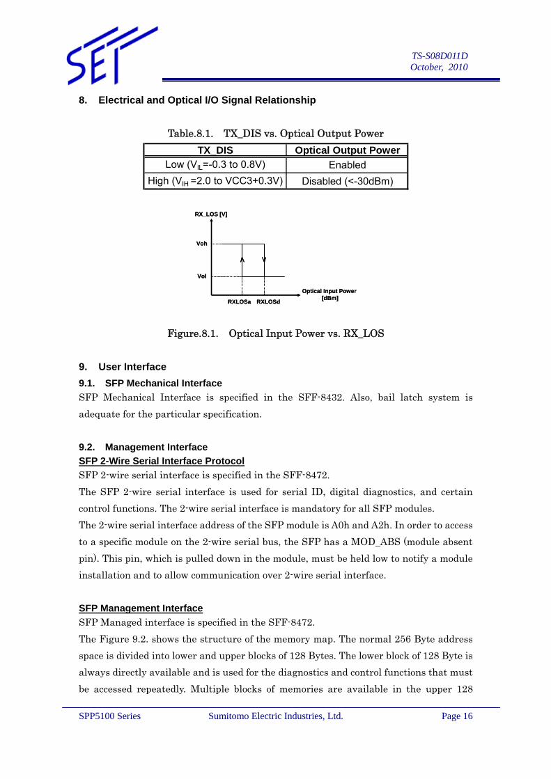
Table.8.1. TX_DIS vs. Optical Output Power TX_DIS Optical Output Power
Low (VIL=-0.3 to 0.8V) EnabledHigh (VIH =2.0 to VCC3+0.3V) Disabled (<-30dBm)
RX_LOS [V]
Optical Input Power[dBm]
Vol
Voh
RXLOSdRXLOSa
RX_LOS [V]
Optical Input Power[dBm]
Vol
Voh
RXLOSdRXLOSa
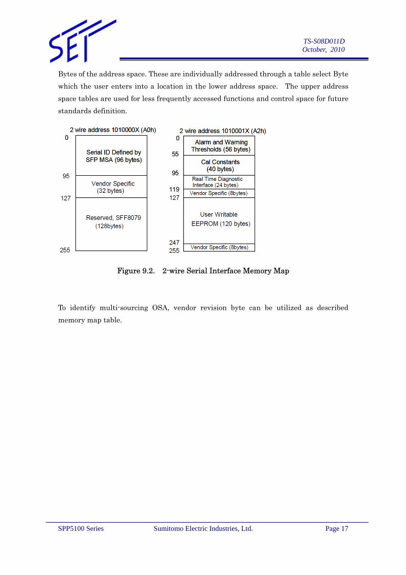
Figure.8.1. Optical Input Power vs. RX_LOS 9. User Interface 9.1. SFP Mechanical Interface SFP Mechanical Interface is specified in the SFF-8432. Also, bail latch system is adequate for the particular specification. 9.2. Management Interface SFP 2-Wire Serial Interface Protocol SFP 2-wire serial interface is specified in the SFF-8472. The SFP 2-wire serial interface is used for serial ID, digital diagnostics, and certain control functions. The 2-wire serial interface is mandatory for all SFP modules. The 2-wire serial interface address of the SFP module is A0h and A2h. In order to access to a specific module on the 2-wire serial bus, the SFP has a MOD_ABS (module absent pin). This pin, which is pulled down in the module, must be held low to notify a module installation and to allow communication over 2-wire serial interface. SFP Management Interface SFP Managed interface is specified in the SFF-8472. The Figure 9.2. shows the structure of the memory map. The normal 256 Byte address space is divided into lower and upper blocks of 128 Bytes. The lower block of 128 Byte is always directly available and is used for the diagnostics and control functions that must be accessed repeatedly. Multiple blocks of memories are available in the upper 128
TS-S08D011D October, 2010
SPP5100 Series Sumitomo Electric Industries, Ltd. Page 17
Bytes of the address space. These are individually addressed through a table select Byte which the user enters into a location in the lower address space. The upper address space tables are used for less frequently accessed functions and control space for future standards definition.
Figure 9.2. 2-wire Serial Interface Memory Map To identify multi-sourcing OSA, vendor revision byte can be utilized as described memory map table.
TS-S08D011D October, 2010
SPP5100 Series Sumitomo Electric Industries, Ltd. Page 18
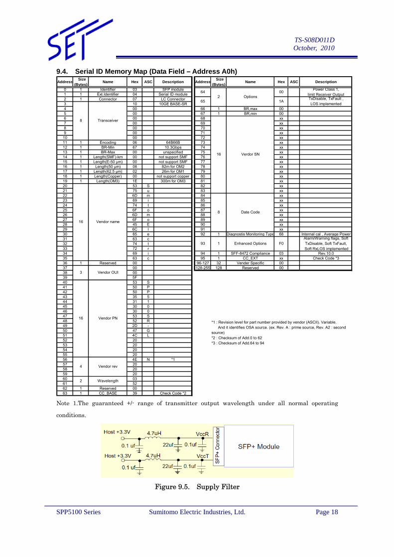
9.4. Serial ID Memory Map (Data Field – Address A0h) Address Size
(Bytes)Name Hex ASC Description Address Size
(Bytes)Name Hex ASC Description
0 1 Identifier 03 SFP module1 1 Ext.Identifier 04 Serial ID module2 1 Connector 07 LC Connector3 10 10GE BASE-SR4 00 66 1 BR,max 005 00 67 1 BR,min 006 00 68 xx7 00 69 xx8 00 70 xx9 00 71 xx
10 00 72 xx11 1 Encoding 06 64B66B 73 xx12 1 BR-Min 67 10.3Gbps 74 xx13 1 BR-Max 00 unspecified 75 xx14 1 Length(SMF)-km 00 not support SMF 76 xx15 1 Length(E-50 μm) 00 not support SMF 77 xx16 1 Length(50 μm) 08 82m for OM2 78 xx17 1 Length(62.5 μm) 02 26m for OM1 79 xx18 1 Length(Copper) 00 not support copper 80 xx19 1 Length(OM3) 1E 300m for OM3 81 xx20 53 S 82 xx21 75 u 83 xx22 6D m 84 xx23 69 i 85 xx24 74 t 86 xx25 6F o 87 xx26 6D m 88 xx27 6F o 89 xx28 45 E 90 xx29 6C l 91 xx30 65 e 92 1 Diagnostis Monitoring Type 68 Internal cal , Average Power31 63 c32 74 t33 72 r34 69 i 94 1 SFF-8472 Compliance 03 Rev.10.035 63 c 95 1 CC_EXT xx Check Code *336 1 Reserved 00 96-127 32 Vender Specific 0037 00 128-255 128 Reserved 0038 0039 5F40 53 S41 50 P42 50 P43 35 544 31 145 30 046 30 047 53 S48 52 R49 2D -50 47 G51 4C L52 20 53 20 54 20 55 20 56 4E N *157 20 58 20 59 20 60 0361 5262 1 Reserved 0063 1 CC_BASE 39 Check Code *2
2 Options
16 Vendor name
8
8 Transceiver
64
65
93
3 Vendor OUI
*1 : Revision level for part number provided by vendor (ASCII). Variable. And it identifies OSA source. (ex. Rev. A : prime source, Rev. A2 : secondsource)*2 : Checksum of Add.0 to 62*3 : Checksum of Add.64 to 94
16 Vendor PN
4 Vendor rev
2 Wavelength
16 Verdor SN
Date Code
1 Enhanced Options
00
1A
F0Alarm/Warning flags, SoftTxDisable, Soft TxFault,
Soft RxLOS implemented
Power Class 1,limit Receiver OutputTxDisable, TxFault ,LOS implemented
Note 1.The guaranteed +/- range of transmitter output wavelength under all normal operating
conditions.
Figure 9.5. Supply Filter

TS-S08D011D October, 2010
SPP5100 Series Sumitomo Electric Industries, Ltd. Page 19
9.5. Alarm/Warming threshold
A2h address Meaning Unit SPP5101SR-GL0-1 Temperature High Alarm deg 752-3 Temperature Low Alarm deg -54-5 Temperature High Warning deg 706-7 Temperature Low Warning deg 08-9 Voltage High Alarm V 3.63
10-11 Voltage Low Alarm V 2.9712-13 Voltage High Warning V 3.46514-15 Voltage Low Warning V 3.13516-17 Tx Bias High Alarm mA 10.5 (15)18-19 Tx Bias Low Alarm mA 2 (3.4)20-21 Tx Bias High Warning mA 9 (13)22-23 Tx Bias Low Warning mA 2.5 (4.6)24-25 Tx Power High Alarm dBm 1.526-27 Tx Power Low Alarm dBm -11.328-29 Tx Power High Warning dBm -1.530-31 Tx Power Low Warning dBm -7.332-33 Rx Power High Alarm dBm 234-35 Rx Power Low Alarm dBm -13.936-37 Rx Power High Warning dBm -138-39 Rx Power Low Warning dBm -9.9
Note.
- Alarm /Warming flag is linked to TxFault by default setting.
- Tx Bias Alarm/Warming is describing both prime and OSA source.
The parentheses value is second source case.
10. RoHS COMPLIANCY Compliancy versus requirements contained inside the following reference document is guaranteed:”Directive 2002/95/EC of 27 January 2003 on the restriction of the use of certain hazardous substances in electrical and electronic equipment from official journal of European Union (European Parliament and of the Council). This product is Compliant at RoHS-6/6 level and contains no leaded solders. 11. Qualification Testing SPP5100SR-GL 10Gb/s transceiver is qualified to Sumitomo Electric Industries internal design and manufacturing standards. Telecordia GR-468-CORE reliability test standards, using methods per MIL-STD-883 for mechanical integrity, endurance, moisture, flammability and ESD thresholds, are followed.

TS-S08D011D October, 2010
SPP5100 Series Sumitomo Electric Industries, Ltd. Page 20
12. Laser Safety Information
SPP5100SR-GL transceiver uses a semiconductor laser system that is classified as Class 1 laser products per the Laser Safety requirements of FDA/CDRH, 21 CFR1040.10 and 1040.11. These products have also been tested and certified as Class 1 laser products per IEC60825-1:2007 and IEC60825-1:2001 International standards.
Caution _______________________________________________________________________________
If this product is used under conditions not recommended in the specification or is used with
unauthorized revision, the classification for laser product safety is invalid. Reclassify the
product at your responsibility and take appropriate safety measures.
_______________________________________________________________________________ 13. Electromagnetic Compatibility EMI (Emission) SPP5100SR-GL is designed to meet FCC Class B limits for emissions and noise immunity per CENELEC EN50 081 and 082 specifications.
RF Immunity SPP5100SR-GL has an immunity to operate when tested in accordance with IEC 61000-4-3 (80- 1000MHz, Test Level 3) and GR-1089.
Electrostatic Discharge (ESD) Immunity SPP5100SR-GL has an immunity against direct and indirect ESD when tested accordance with IEC 61000-4-2.
TS-S08D011D October, 2010
SPP5100 Series Sumitomo Electric Industries, Ltd. Page 21
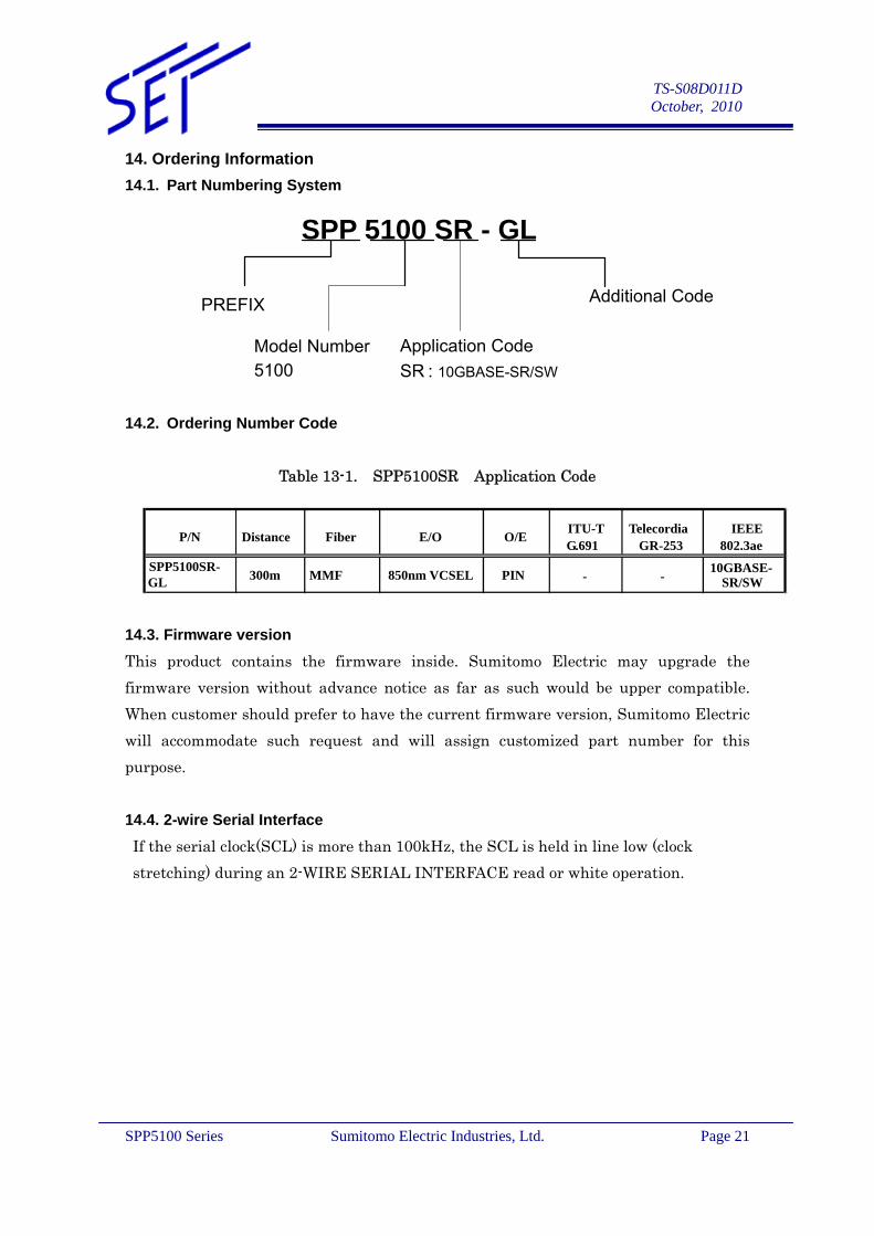
14. Ordering Information 14.1. Part Numbering System 14.2. Ordering Number Code
Table 13-1. SPP5100SR Application Code 14.3. Firmware version This product contains the firmware inside. Sumitomo Electric may upgrade the firmware version without advance notice as far as such would be upper compatible. When customer should prefer to have the current firmware version, Sumitomo Electric will accommodate such request and will assign customized part number for this purpose. 14.4. 2-wire Serial Interface If the serial clock(SCL) is more than 100kHz, the SCL is held in line low (clock stretching) during an 2-WIRE SERIAL INTERFACE read or white operation.
GL SR/SW
SPP 5100 SR - GL
PREFIX
Model Number 5100
Application Code SR : 10GBASE-SR/SW
Additional Code
- - 10GBASE-
P/N Distance Fiber E/O O/E ITU-TG.691
IEEE802.3ae
TelecordiaGR-253
SPP5100SR- 300m MMF 850nm VCSEL PIN

TS-S08D011D October, 2010
SPP5100 Series Sumitomo Electric Industries, Ltd. Page 22
15. Label information 16. Contact Information
U.S.A. Sumitomo Electric Device Innovations, U.S.A., Inc. <West Coast (USA Headquarters)> 2355 Zanker Rd. San Jose, CA 95131-1138, USA Tel: +1-408-232-9500 Fax: +1-408-428-9111 <East Coast> 4021 Stirrup Creek Drive, Suite 200, Durham, NC 27703, USA Tel: +1-919-361-1600 Fax: +1-919-361-1619 Email: [email protected], [email protected] http://www.sei-device.com/ Europe Sumitomo Electric Europe Ltd. 220 Centennial Park, Elstree, Herts, WD6 3SL UK Tel: +44-208-953-8681 Fax: +44-208-207-5950 E-mail: [email protected] http://www.sumielectric.com Asia Sumitomo Electrics Asia Ltd. Photonics Department Room 2624 - 2637, 26F., Sun Hung Kai Center, 30 Harbour Road, Wanchai, Hongkong. Tel: +852-2576-0080 Fax: +852-2576-6412 Japan Sumitomo Electric Industries, Ltd. Device Sales Department <Tokyo> 3-9-1, Shibaura, Minato-ku, Tokyo 108-8539, Japan TEL +81-3-6722-3286 FAX +81-3-6722-3284 <Osaka> 4-5-33, Kitahama, Chuo-ku, Osaka 541-0041, Japan Tel: +81-6-6220-4245 Fax: +81-6-6222-6231
E-mail: [email protected] http://www.sei.co.jp/products/index.html


