
1/42
Changkun Park
Title
Dual mode RF CMOS Power Amplifier with transformer for
polar transmitters
March. 26, 2007
Changkun Park
Wave Embedded Integrated Systems (WEIS) Lab.Wave Embedded Integrated Systems (WEIS) Lab.School of Electrical Engineering and Computer ScienceSchool of Electrical Engineering and Computer Science
Korea Advanced Institute of Science and Technology (KAIST)Korea Advanced Institute of Science and Technology (KAIST)

2/42
Changkun Park
Contents
Introduction / Motivation1. Efficiency of polar transmitter
2. Voltage combining technique
Variable Load Technique Proposed Stage-Convertible Power Amplifier
1. Power amplifier with three-port transformer
2. Power amplifier with dual-primary transformer
Proposed Tournament-Shaped Power Combiner1. Theory of tournament-shaped power combiner
2. Circuit design
Conclusions
3/42
Changkun Park
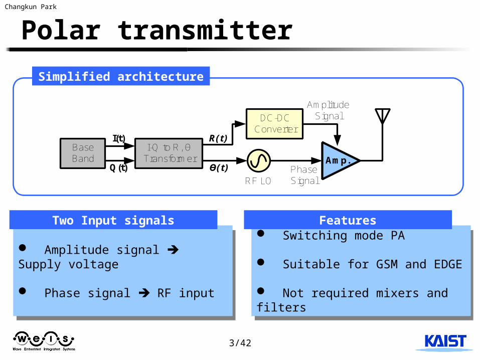
Polar transmitter
Base Band
I-Q to R, ӨTransformer
I(t)
Q(t)
R(t)
DC-DCConverter
Amp.
RF LO
Ө(t) PhaseSignal
AmplitudeSignal
Amplitude signal Supply voltage
Phase signal RF input
Amplitude signal Supply voltage
Phase signal RF input
Switching mode PA
Suitable for GSM and EDGE
Not required mixers and filters
Switching mode PA
Suitable for GSM and EDGE
Not required mixers and filters
Two Input signals Features
Simplified architecture
4/42
Changkun Park
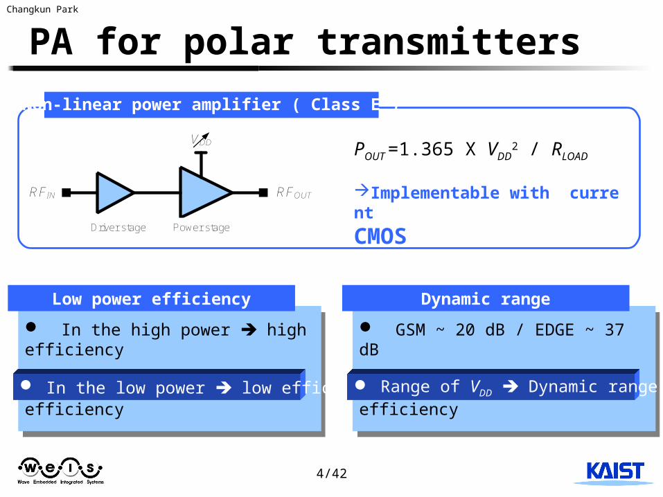
PA for polar transmitters
In the high power high efficiency
In the low power low efficiency
In the high power high efficiency
In the low power low efficiency
RFIN RFOUT
VDD
Driver stage Power stage
POUT =1.365 X VDD2 / RLOAD
Implementable with currentCMOS
Non-linear power amplifier ( Class E )
Low power efficiency
GSM ~ 20 dB / EDGE ~ 37 dB
In the low power low efficiency
GSM ~ 20 dB / EDGE ~ 37 dB
In the low power low efficiency
Dynamic range
In the low power low efficiency Range of VDD Dynamic range
5/42
Changkun Park
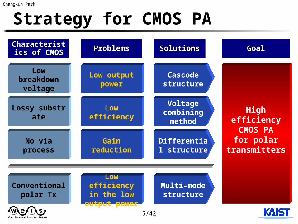
Strategy for CMOS PA
Low breakdown
voltage
Characteristics Characteristics of CMOSof CMOS ProblemsProblems
Low output power
SolutionsSolutions
Lossy substrate
Low efficiency
No via process Gain reduction
High efficiency CMOS PAfor polar
transmitters
GoalGoal
Conventional polar Tx
Low efficiency in the low
output power
Cascode structure
Voltage combining
method
Differential structure
Multi-mode structure
6/42
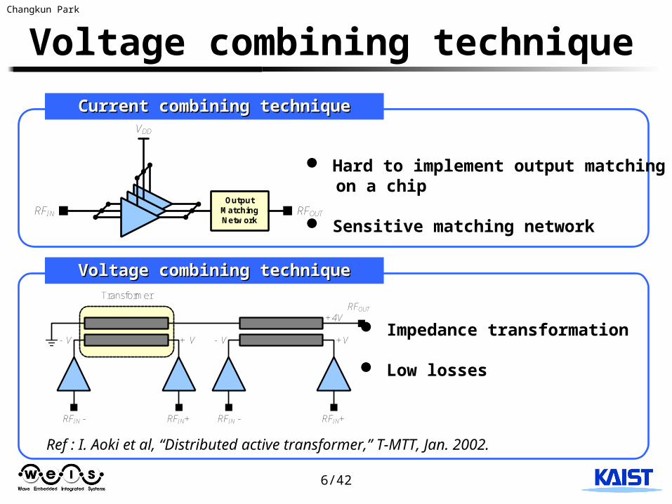
Changkun ParkVoltage combining technique
Output Matching Network
VDD
RFIN RFOUT
RFOUT
RFIN - RFIN+ RFIN - RFIN+
Transformer
- V + V - V +V
+4V
Current combining techniqueCurrent combining technique
Voltage combining techniqueVoltage combining technique
Hard to implement output matching on a chip
Sensitive matching network
Impedance transformation
Low losses
Ref : I. Aoki et al, “Distributed active transformer,” T-MTT, Jan. 2002.
7/42
Changkun Park
Contents
Introduction / Motivation1. Efficiency of polar transmitter
2. Voltage combining technique
Variable Load Technique Proposed Stage-Convertible Power Amplifier
1. Power amplifier with three-port transformer
2. Power amplifier with Dual-primary transformer
Proposed Tournament-Shaped Power Combiner1. Theory of tournament-shaped power combiner
2. Circuit design
Conclusion
8/42
Changkun Park
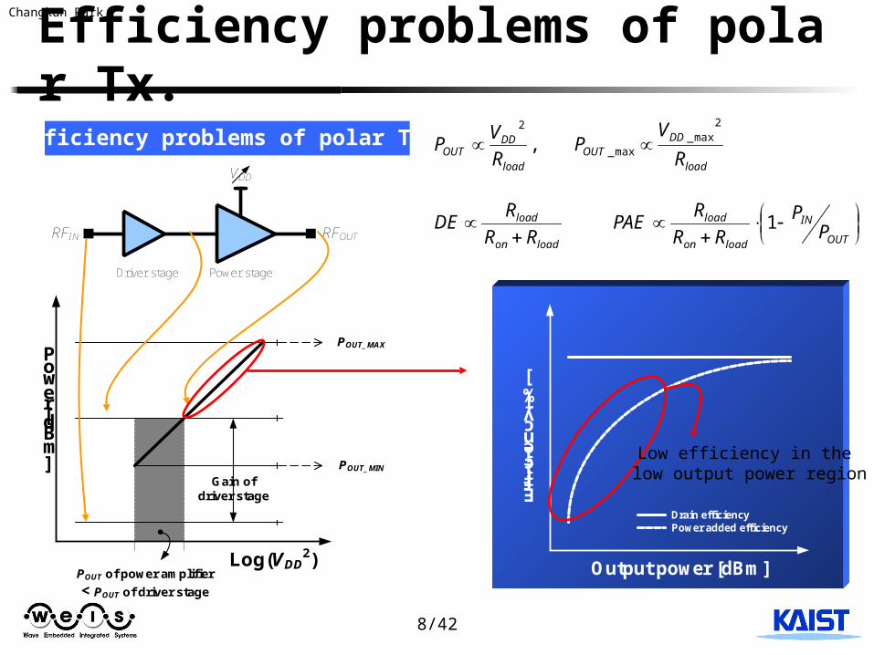
Efficiency problems of polar Tx.
RFIN RFOUT
VDD
Driver stage Power stage
Log(VDD2)
Power [dBm]
Gain of driver stage
POUT of power amplifier
< POUT of driver stage
POUT_MIN
POUT_MAX
Output power [dBm]
Efficiency [%]
Drain efficiencyPower added efficiency
Efficiency problems of polar Tx.
Low efficiency in the low output power region
load
DDOUT
load
DDOUT R
VP
R
VP
2max_
max_
2
,
loadon
load
RR
RDE
OUT
IN
loadon
load
PP
RR
RPAE 1
9/42
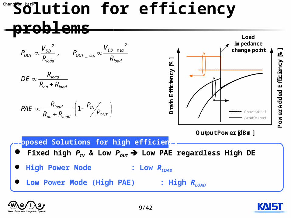
Changkun ParkSolution for efficiency problems
Dra
in E
ffic
ien
cy
[%
]
Po
we
r A
dd
ed
Eff
icie
nc
y [
%]
Output Power [dBm]
Load impedance
change point
Conventional
Variable Load
Fixed high PIN & Low POUT Low PAE regardless High DE
High Power Mode : Low RLOAD
Low Power Mode (High PAE) : High RLOAD
Proposed Solutions for high efficiency
loadon
load
RR
RDE
load
DDOUT
load
DDOUT R
VP
R
VP
2max_
max_
2
,
OUT
IN
loadon
load
PP
RR
RPAE 1
10/42
Changkun Park
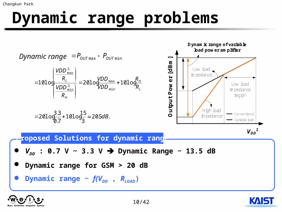
Dynamic range problems
VDD : 0.7 V ~ 3.3 V Dynamic Range ~ 13.5 dB
Dynamic range for GSM > 20 dB
Dynamic range ~ f(VDD , RLOAD)
Proposed Solutions for dynamic range
Conventional
Variable load
Outp
ut
Pow
er
[dBm
]
VDD2
Low load impedance
region
High load impedance
Low load impedance
Dynamic range of variable load power amplifier
Dynamic range minmax OUTOUT PP
.5.203
15log10
7.0
3.3log20
log10log20log10min
max2min
2max
dB
R
R
VDD
VDD
RVDD
R
VDD
L
H
H
L
11/42
Changkun Park
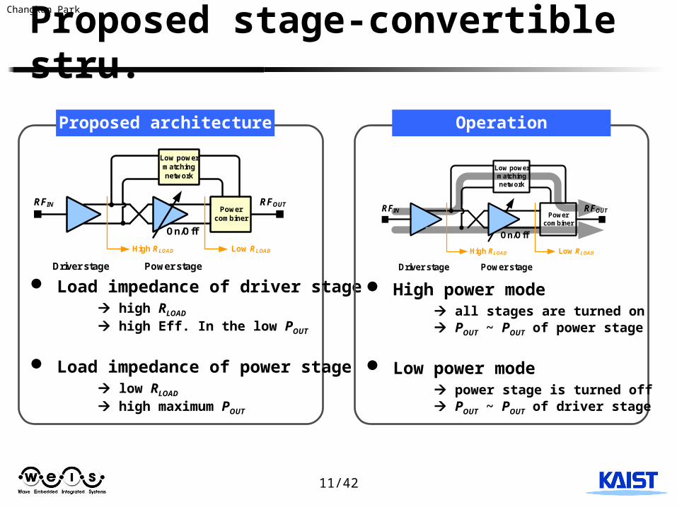
Proposed stage-convertible stru.
Power combiner
On/Off
Power stageDriver stage
RFIN RFOUT
High RLOAD Low RLOAD
Low power matching network
Load impedance of driver stage high RLOAD high Eff. In the low POUT
Load impedance of power stage low RLOAD high maximum POUT
Proposed architecture
High power mode all stages are turned on POUT ~ POUT of power stage
Low power mode power stage is turned off POUT ~ POUT of driver stage
Operation
Power combiner
On/Off
Power stageDriver stage
RFIN RFOUT
High RLOAD Low RLOAD
Low power matching network
12/42
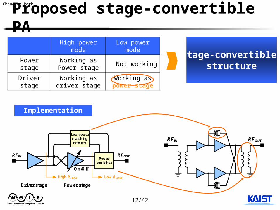
Changkun ParkProposed stage-convertible PA
Implementation
RFIN RFOUT
Power combiner
On/Off
Power stageDriver stage
RFIN RFOUT
High RLOAD Low RLOAD
Low power matching network
High power mode Low power mode
Power stageWorking as Power stage
Not working
Driver stageWorking as driver
stageWorking as
power stage
Stage-convertible structure
13/42
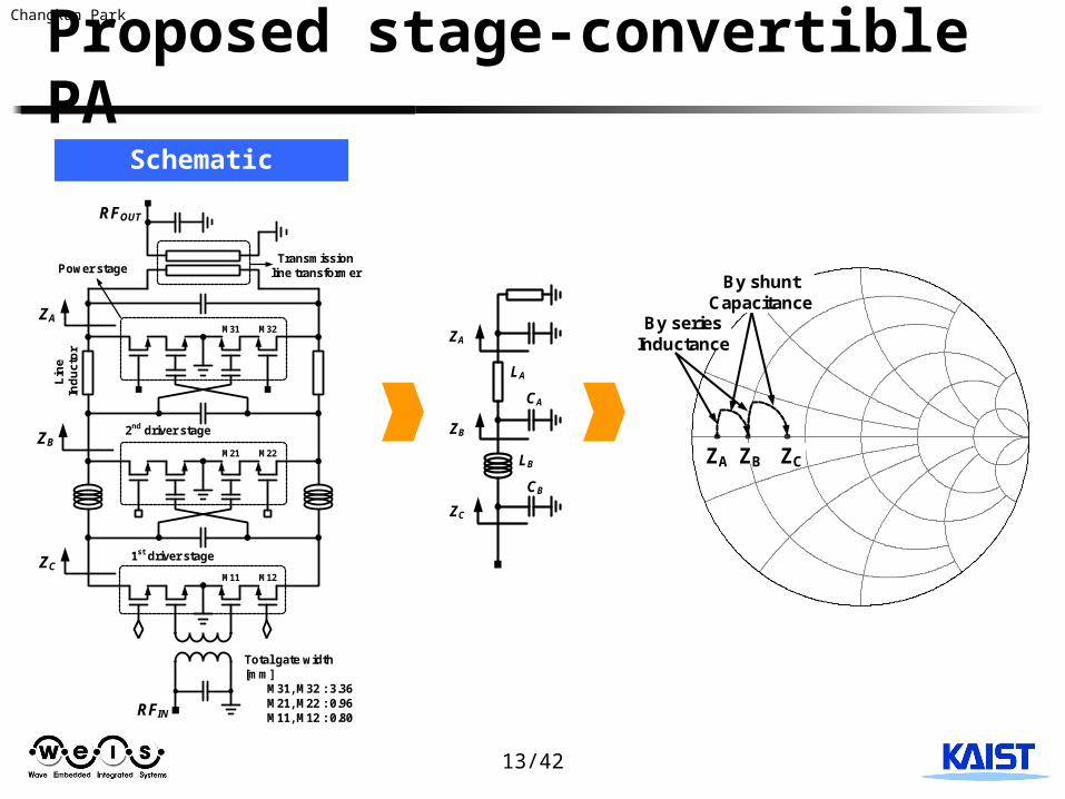
Changkun ParkProposed stage-convertible PA
Lin
e
Ind
uc
tor
ZA
ZB
ZC1st driver stage
Power stage
2nd driver stage
M11 M12
M21 M22
M31 M32
Transmission line transformer
RFIN
RFOUT
Total gate width [mm] M31, M32 : 3.36 M21, M22 : 0.96 M11, M12 : 0.80
ZC
ZB
ZA
LA
CA
LB
CB
ZA ZB ZC
By series Inductance
By shunt Capacitance
Schematic
14/42
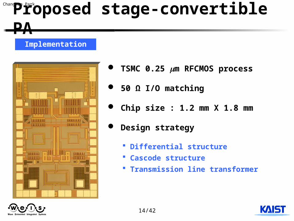
Changkun ParkProposed stage-convertible PA
Implementation
TSMC 0.25 m RFCMOS process
50 Ω I/O matching
Chip size : 1.2 mm X 1.8 mm
Design strategy
Differential structure Cascode structure Transmission line transformer
15/42
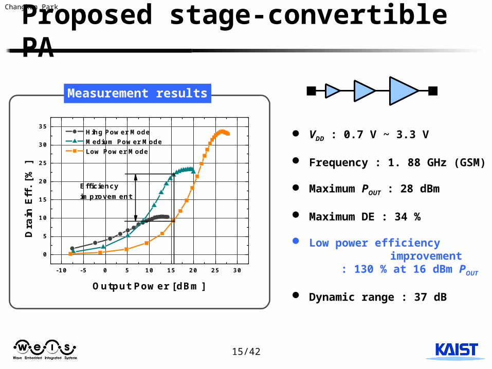
Changkun ParkProposed stage-convertible PA
VDD : 0.7 V ~ 3.3 V
Frequency : 1. 88 GHz (GSM)
Maximum POUT : 28 dBm
Maximum DE : 34 %
Low power efficiency improvement
: 130 % at 16 dBm POUT
Dynamic range : 37 dB
-10 -5 0 5 10 15 20 25 30
0
5
10
15
20
25
30
35
Dra
in E
ff. [%
]
Output Power [dBm]
Hihg Power Mode Medium Power Mode Low Power Mode
Efficiencyimprovement
Measurement results
16/42
Changkun ParkProposed stage-convertible PA
Contributions
Problems of PA for polar transmitters are analyzed.
Stage-convertible structure is proposed.
Variable load technique is used.
Low efficiency at low output power region is improved.
Ref : Changkun Park et al, “Power Amplifier,” patent registered num. Korea, 2007. Changkun Park et al, “Power amplifier using 3-port transmission line transformer,” patent pending.
Korea / USA / Japan / China, 2006. Changkun Park et al, “A 1.9-GHz Triple-Mode Class-E Power Amplifier for a Polar Transmitter,” MWCL, Feb. 2007.

17/42
Changkun Park
Contents
Introduction / Motivation1. Efficiency of polar transmitter
2. Voltage combining technique
Variable Load Technique Proposed Stage-Convertible Power Amplifier
1. Power amplifier with three-port transformer
2. Power amplifier with Dual-primary transformer
Proposed Tournament-Shaped Power Combiner1. Theory of tournament-shaped power combiner
2. Circuit design
Conclusion
18/42
Changkun Park
Proposed SC PA using TLT
C
(1-k)L1 = La (1-k)L2 = Lb
kL1 = LM
Transformer
Cshunt RT
RLOAD RaRb
CshuntC RT
RLOAD 1:1 Transformer
.)(1
)(1
2
2222
2
shuntT
shuntTshuntbTb
shuntT
Ta
CR
CRCLRLj
CR
RR
.)(1 2
2
shuntT
shuntTb CR
CRL
222
2
222
22
Ma
Ma
Ma
Ma
Ma
Mab LR
LRj
LR
LR
LjR
LRjR
.)1()(1 2222222
22
CLLLLCR
LRR
aMMaa
MaLOAD
Impedance transformation using transmission line transformer
19/42
Changkun Park
Proposed SC PA using TLT
Imp
ed
an
ce
, RL
OA
D []
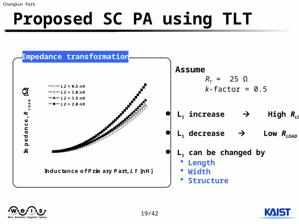
Inductance of Primary Part, L1 [nH]
L2 = 0.5 nH L2 = 1.0 nH L2 = 1.5 nH L2 = 2.0 nH
Assume RT = 25 Ωk-factor = 0.5
L1 increase High RLOAD
L1 decrease Low RLOAD
L1 can be changed by Length Width Structure
Impedance transformation
20/42
Changkun Park
Proposed SC PA using TLT
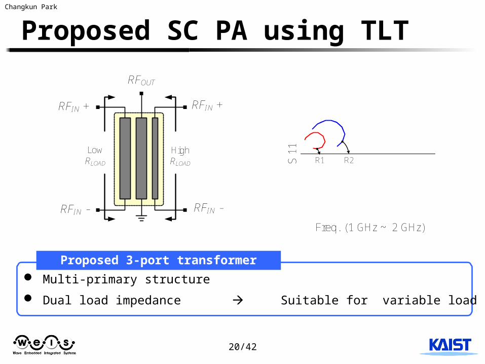
RFOUT
RFIN +
RFIN -
Low RLOAD
High RLOAD
RFIN +
RFIN -
freq (1.000GHz to 2.000GHz)
S(1
,1)
freq (1.000GHz to 2.000GHz)
S(1
,1)
freq (1.000GHz to 2.000GHz)
S(1
,1)
freq (1.000GHz to 2.000GHz)
S(1
,1)
S 11
Freq. (1 GHz ~ 2 GHz)
R1 R2
Multi-primary structure
Dual load impedance Suitable for variable load PA
Proposed 3-port transformer

21/42
Changkun Park
Proposed SC PA using TLT
Low power matching network
Power combiner
On/Off
Power stageDriver stage
RFIN RFOUT
3-port transmission line transformer
RFIN + RFIN -
RFOUT
High power stage Low power stage / Driver stage
In phaseLow RLOAD
High RLOAD
All of the stages are turned on
Driver stage drives the power stage
Low RLOAD High maximum POUT
High power mode Power stage is turned off
POUT of Driver stage = POUT of PA
High RLOAD
Efficiency & Dynamic range increase
Low power mode
22/42
Changkun Park
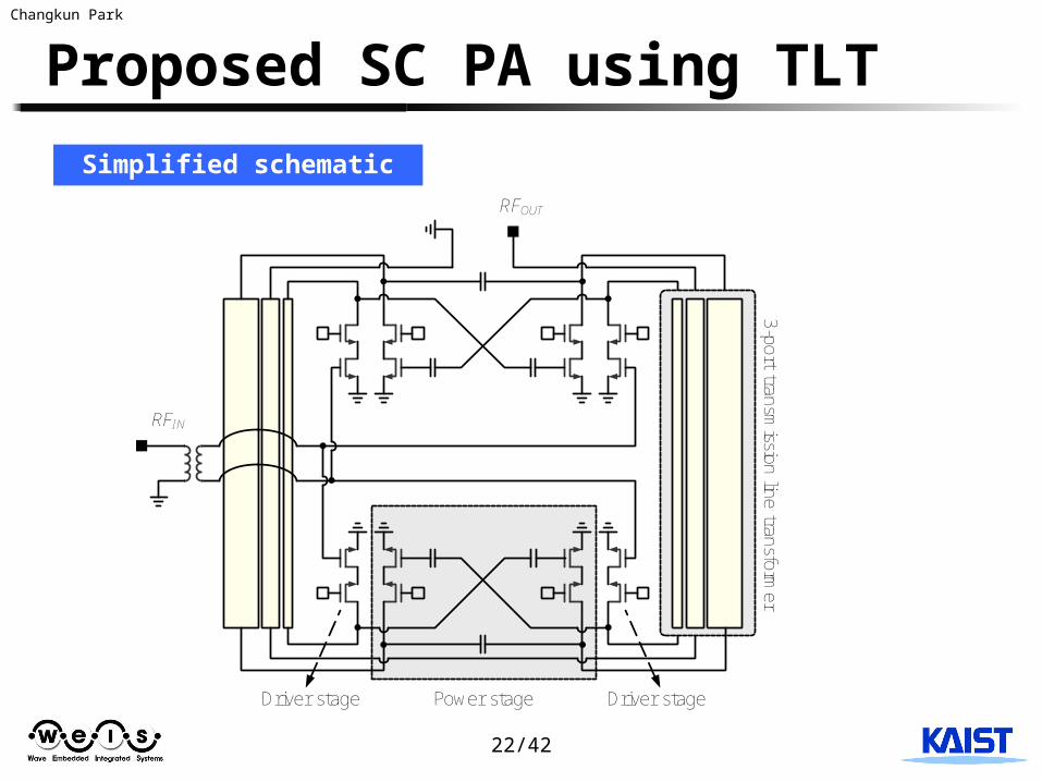
Proposed SC PA using TLT
Power stageDriver stage
RFIN
RFOUT
Driver stage
3-port transmission line transform
er
Simplified schematic
23/42
Changkun Park
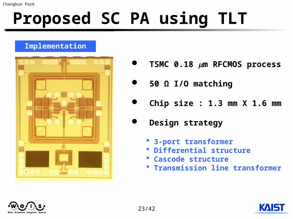
Proposed SC PA using TLT
TSMC 0.18 m RFCMOS process
50 Ω I/O matching
Chip size : 1.3 mm X 1.6 mm
Design strategy
3-port transformer Differential structure Cascode structure Transmission line transformer
Implementation

24/42
Changkun Park
Proposed SC PA using TLT
Power Stage
POUT
Driver Stage
PIN
VDD VDD
Turn off
Power Stage
POUT
Driver Stage
PIN
VDD VDD
Power Stage
POUT
Driver Stage
PIN
VDD VDD
High power mode Low power mode Auto-switching mode
0.5 1.0 1.5 2.0 2.5 3.0 3.5
5
10
15
20
25
30
Ga
in [
dB
]
Supply voltage, VDD
[V]
High power mode Low power mode auto-switching mode
Mode change region
Frequency : 1. 9 GHz
Pin = 6.19 dBm
Supply voltage : 0.5 ~ 3.3 V
25/42
Changkun Park
10 15 20 25 30 350
5
10
15
20
25
30
35
40
45
Po
we
r A
dd
ed
Eff
icie
nc
y [
%]
Output Power, POUT
[dBm]
High power mode Low power mode With auto-switching method
Efficiencyimprovement at 16 dBm
0.5 1.0 1.5 2.0 2.5 3.0 3.5
10
15
20
25
30
35
Dynamic range of this work
Dynamic rangeof conventional Class-E
Ou
tpu
t P
ow
er
[dB
m]
VDD
[V]
Conventional Class-E This work
Extension ofdynamic range
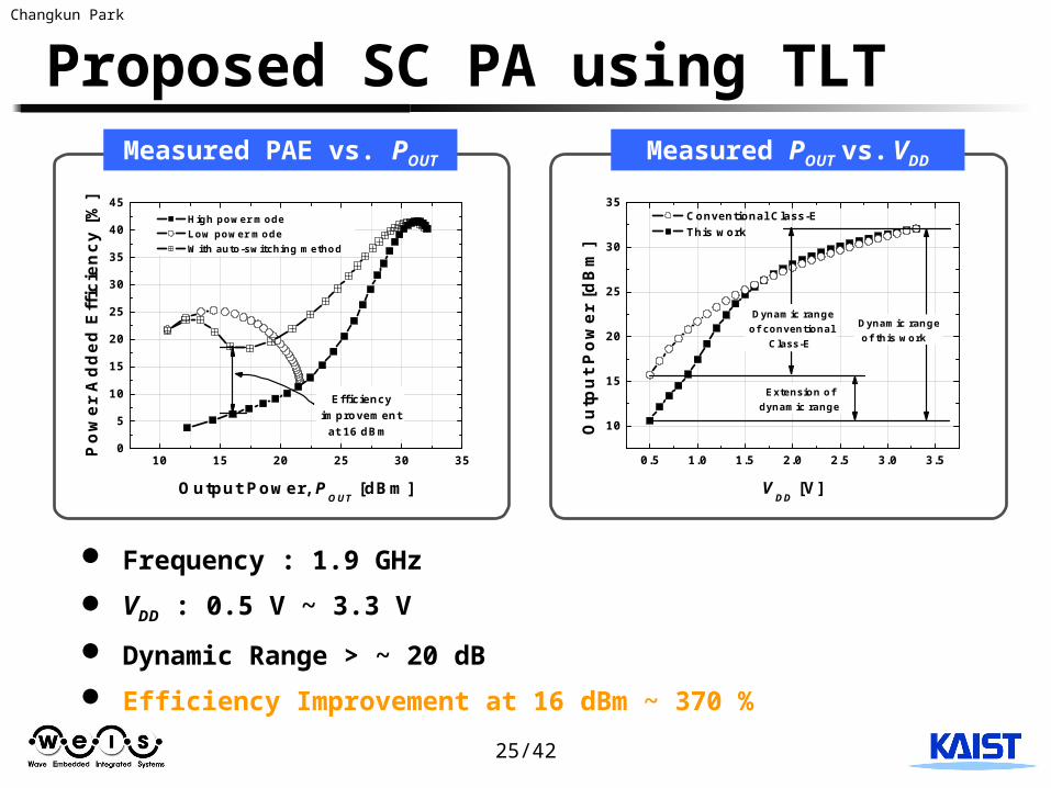
Proposed SC PA using TLTMeasured PAE vs. POUT Measured POUT vs. VDD
Frequency : 1.9 GHz
VDD : 0.5 V ~ 3.3 V
Dynamic Range > ~ 20 dB
Efficiency Improvement at 16 dBm ~ 370 %

26/42
Changkun ParkProposed stage-convertible PA
Contributions
Transmission line transformer is analyzed. Impedance transformations using parasitic
components of transmission line transformer
Stage-convertible structure using TLT is proposed. 3-port asymmetric transformer is proposed.
Output power is increased.
Ref : Changkun Park et al, “Transmission line transformer,” patent registered. Korea, 2007. Changkun Park et al, “Transmission line transformer,” patent pending. USA / Japan, 2006. Changkun Park et al, “A 1.9-GHz CMOS Power Amplifier Using Three-Port Asymmetric Transmission Line
Transformer for a Polar Transmitter,” T-MTT, Feb. 2007. published.
27/42
Changkun Park
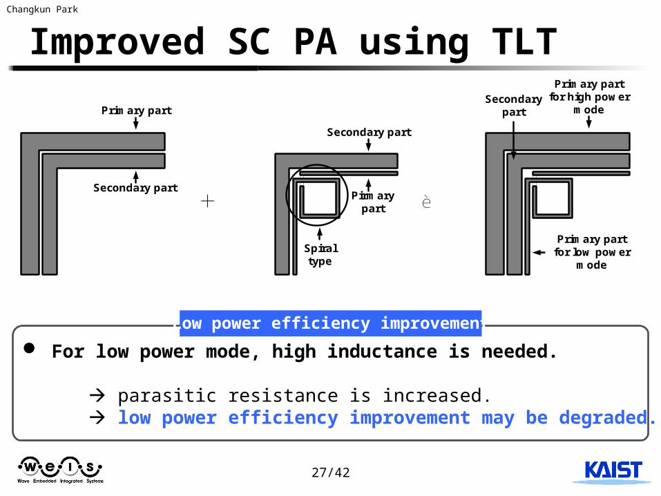
Improved SC PA using TLT
è +
Primary part
Secondary part
Secondary part
Pirmary part
Secondary part
Primary partfor high power
mode
Primary partfor low power
mode
Spiral type
For low power mode, high inductance is needed.
parasitic resistance is increased. low power efficiency improvement may be degraded.
Low power efficiency improvement

28/42
Changkun Park
Improved SC PA using TLT
-V+V
0
4VI
0.5 I
0.5 I
RFOUT
Impedance transformation ratio 1:8
Very small size (transformer)1000 m X 1000 m (previous work) 670 m X 510 m
0.5 I
0.5 I
I-V V
0
4V
RT = 50 ΩRLOAD
High power mode
50:25.68:15.0
4::
I
V
I
VRR TLOAD

29/42
Changkun Park
Improved SC PA using TLT
aI
I
aI
-V V
0
βV
DistanceγV
RT = 50 Ω
RLOAD
15.0 a 42 20 82 a
50:252:1
:1::a
a
I
V
I
VRR TLOAD
Low power mode
RFOUT
AB
RFIN + RFIN -
A B
30/42
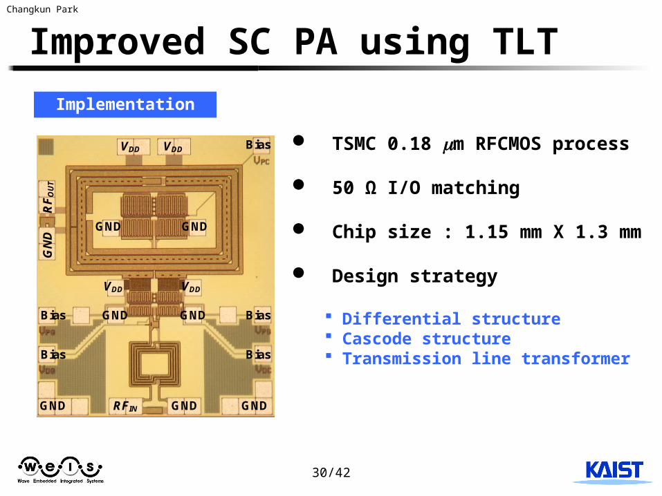
Changkun Park
Improved SC PA using TLT
GNDRFINGND GND
RF
OU
TG
ND
VDDVDD
GND GND
GND GND
VDD VDD
Bias Bias
Bias Bias
Bias TSMC 0.18 m RFCMOS process
50 Ω I/O matching
Chip size : 1.15 mm X 1.3 mm
Design strategy
Differential structure Cascode structure Transmission line transformer
Implementation

31/42
Changkun Park
Improved SC PA using TLT
10 15 20 25 30 350
5
10
15
20
25
30
35
40
45
Dra
in e
ffic
ien
cy
[%]
Output power [dBm]
Low power mode High power mode Auto-switching mode
1.7 1.8 1.9 2.024
26
28
30
32
34
Ou
tpu
t p
ow
er [
dB
m]
Frequency [GHz]
Frequency sweep V
DD of power amplifier : 3.3 V
Frequency : 1.8 GHz
VDD : 0.5 V ~ 3.3 V
Dynamic Range ~ 20 dB
Efficiency at 16 dBm ~ 33 %
PIN = 10 dBm
VDD = 3.3 V (Maximum POUT condition)
Gain at 1.8 GHz = 21.6 dB
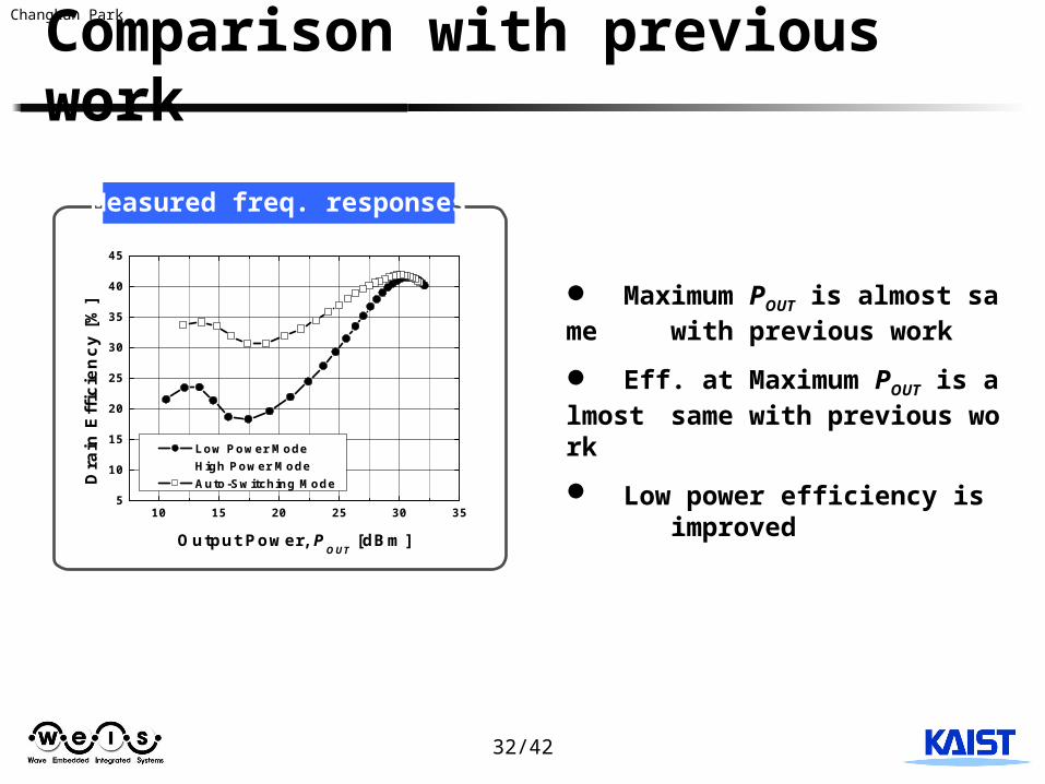
Measured freq. responses Reliability at maximum POUT
32/42
Changkun ParkComparison with previous work
10 15 20 25 30 355
10
15
20
25
30
35
40
45
Dra
in E
ffic
ien
cy [
%]
Output Power, POUT
[dBm]
Low Power Mode High Power Mode Auto-Switching Mode
Maximum POUT is almost same with previous work
Eff. at Maximum POUT is almost same with previous work
Low power efficiency is improved
Measured freq. responses
33/42
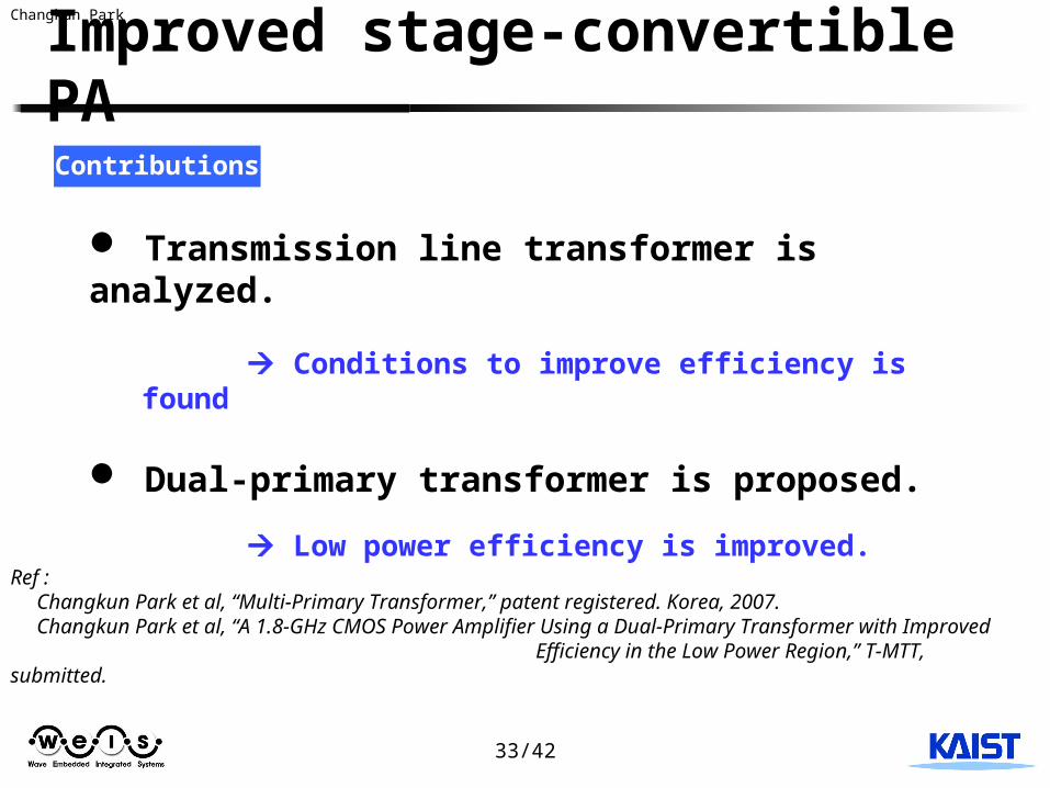
Changkun ParkImproved stage-convertible PA
Contributions
Transmission line transformer is analyzed.
Conditions to improve efficiency is found
Dual-primary transformer is proposed.
Low power efficiency is improved.
Ref : Changkun Park et al, “Multi-Primary Transformer,” patent registered. Korea, 2007. Changkun Park et al, “A 1.8-GHz CMOS Power Amplifier Using a Dual-Primary Transformer with Improved
Efficiency in the Low Power Region,” T-MTT, submitted.

34/42
Changkun Park
Contents
Introduction / Motivation1. Efficiency of polar transmitter
2. Voltage combining technique
Variable Load Technique Proposed Stage-Convertible Power Amplifier
1. Power amplifier with three-port transformer
2. Power amplifier with Dual-primary transformer
Proposed Tournament-Shaped Power Combiner1. Theory of tournament-shaped power combiner
2. Circuit design
Conclusion

35/42
Changkun ParkProposed Tournament combiner
Power splitter
Differential input
RFOUTGND
RFIN -
RFIN +
Input feed line
Differential pair
Feed-line isolation problem
Distributed active transformer
RFIN + RFIN -
RFOUT
-V +V
2V
I
I
1:1 Transmission Line Transformer
RLOAD RLOADRT
0V
1:1 Transmission Line Transformer
RFIN -
RT
RFIN + I
I
RLOAD
-V
+V
0
2V
RLOAD
RFOUT
Another solutions
36/42
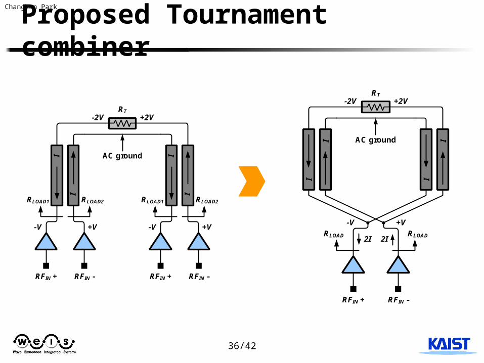
Changkun ParkProposed Tournament combiner
RFIN + RFIN -
I
I
RLOAD2
-V
RLOAD1
RFIN + RFIN -
RLOAD2RLOAD1
AC ground
I
I
RT
+V -V +V
-2V +2V
RFIN + RFIN -
I
I AC ground
I
I
RT
-2V +2V
RLOAD RLOAD2I2I
-V +V
37/42
Changkun ParkProposed Tournament combiner
RFIN + RFIN -
I
I AC ground
-2V +2V
RLOAD RLOAD2I2I
-V +V
I
I
I
I
RFIN + RFIN -
I
I AC ground
-2V +2V
RLOAD RLOAD2I2I
-V +V
I
I
I
I
RT
Current combining
-4V
2I
Tournament shapedPower combiner
VDD_Driver
RFOUTGND
RFIN
Spiral transformer
Driver stage
Power stage
CIN
CINTER
CP_IN
CP_OUT
COUTCGND
Conventional
Input transformer
MD1
MD2
MP1
MP2
VDD
MD1
MD2
MP1
MP2
Cgs
Total gate width [mm] MD1 : 2.048 MD2 : 4.096 MP1 : 4.096 MP2 : 5.120

38/42
Changkun ParkProposed Tournament combiner
TSMC 0.18 m RFCMOS process
Fully integrated PA with 50 Ω I/O matching
Chip size : 1.2 mm X 2.0 mm
Design strategy
Tournament-shaped power combiner Differential structure Cascode structure
Implementation
39/42
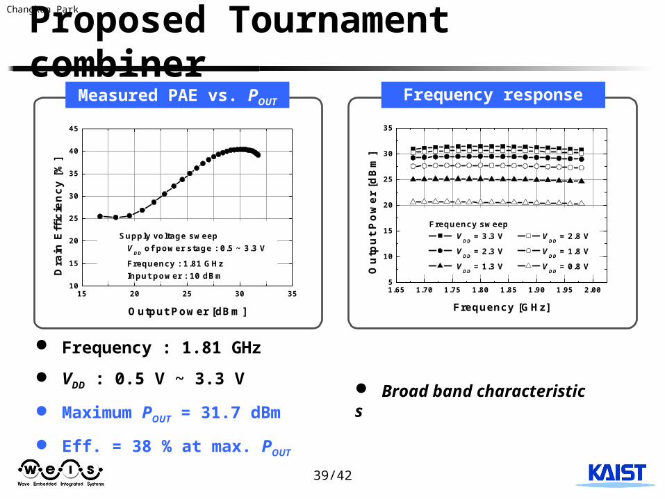
Changkun ParkProposed Tournament combiner
15 20 25 30 3510
15
20
25
30
35
40
45
Dra
in E
ffic
ien
cy [
%]
Output Power [dBm]
Supply voltage sweep V
DD of power stage : 0.5 ~ 3.3 V
Frequency : 1.81 GHz Input power : 10 dBm
1.65 1.70 1.75 1.80 1.85 1.90 1.95 2.005
10
15
20
25
30
35
Ou
tpu
t P
ow
er
[dB
m]
Frequency [GHz]
Frequency sweep V
DD = 3.3 V V
DD = 2.8 V
VDD
= 2.3 V VDD
= 1.8 V
VDD
= 1.3 V VDD
= 0.8 V
Frequency : 1.81 GHz
VDD : 0.5 V ~ 3.3 V
Maximum POUT = 31.7 dBm
Eff. = 38 % at max. POUT
Broad band characteristics
Measured PAE vs. POUT Frequency response
40/42
Changkun ParkProposed Tournament combiner
Contributions
Tournament-shaped power combiner is proposed.
Isolation problems between TLT and input feed-line are solved.
Ref : Changkun Park et al, “Power amplifier used power combiner,” patent pending. Korea, 2007. Changkun Park et al, “Tournament-Shaped Magnetically Coupled Power Combiner Architecture for
RF CMOS Power Amplifier,” T-MTT, submitted.
41/42
Changkun Park
Conclusions
PA for polar transmitter– Efficiency characteristics are analyzed.
Transformers for dual-mode power amplifier– Power amplifier with 3-port transformer is proposed.– Power amplifier with dual-primary transformer is proposed.
New power combiner– Tournament-shaped power combiner is proposed.
42/42
Changkun Park
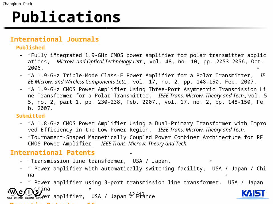
Publications International Journals
Published– “Fully integrated 1.9-GHz CMOS power amplifier for polar transmitter applications,” Microw. and Optical Tec
hnology Lett., vol. 48, no. 10, pp. 2053-2056, Oct. 2006.
– “A 1.9-GHz Triple-Mode Class-E Power Amplifier for a Polar Transmitter,” IEEE Microw. and Wireless Components Lett., vol. 17, no. 2, pp. 148-150, Feb. 2007.
– “A 1.9-GHz CMOS Power Amplifier Using Three-Port Asymmetric Transmission Line Transformer for a Polar Transmitter,” IEEE Trans. Microw. Theory and Tech., vol. 55, no. 2, part 1, pp. 230-238, Feb. 2007., vol. 17, no. 2, pp. 148-150, Feb. 2007.
Submitted– “A 1.8-GHz CMOS Power Amplifier Using a Dual-Primary Transformer with Improved Efficiency in the Low
Power Region,” IEEE Trans. Microw. Theory and Tech.
– “Tournament-Shaped Magnetically Coupled Power Combiner Architecture for RF CMOS Power Amplifier,” IEEE Trans. Microw. Theory and Tech.
International Patents – “Transmission line transformer,” USA / Japan.
– “ Power amplifier with automatically switching facility,” USA / Japan / China
– “ Power amplifier using 3-port transmission line transformer,” USA / Japan / China
– “ Power amplifier,” USA / Japan / France
Domestic Patents - 16
43/42
Changkun Park
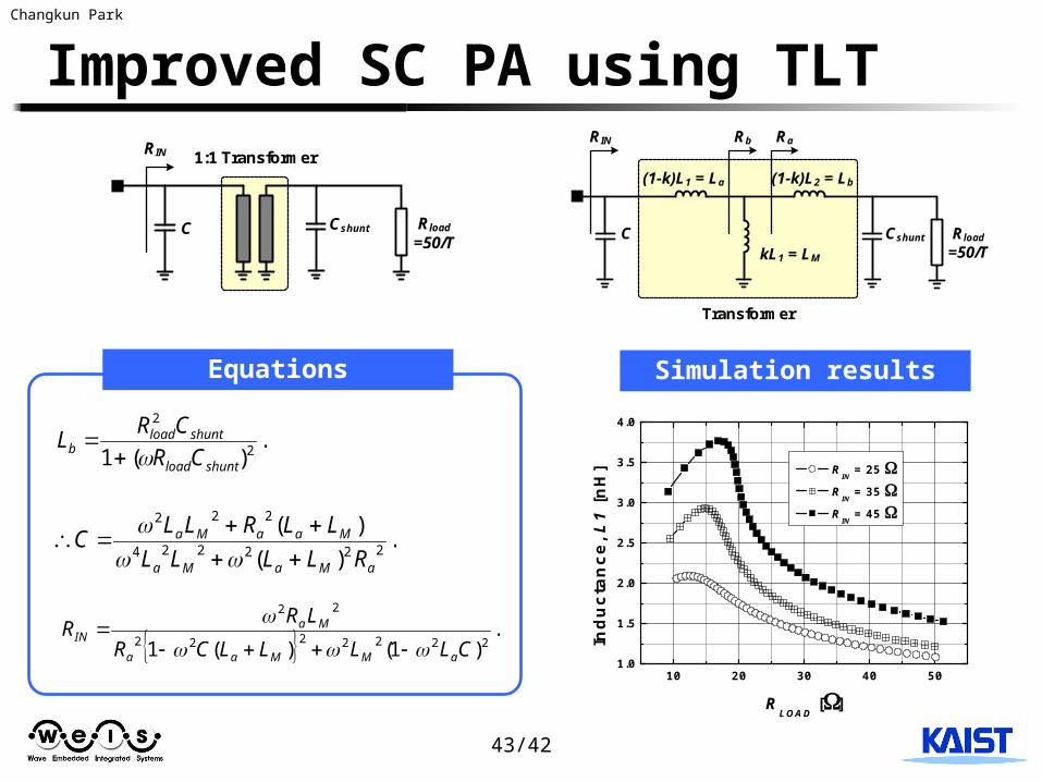
Improved SC PA using TLT
10 20 30 40 501.0
1.5
2.0
2.5
3.0
3.5
4.0
Ind
uct
ance
, L1
[nH
]
RLOAD
[]
RIN
= 25
RIN
= 35
RIN
= 45
Simulation results
.)(1 2
2
shuntload
shuntloadb CR
CRL
.)(
)(222224
222
aMaMa
MaaMa
RLLLL
LLRLLC
.)1()(1 2222222
22
CLLLLCR
LRR
aMMaa
MaIN
Equations
CshuntC Rload
=50/T
RIN 1:1 Transformer
C
(1-k)L1 = La (1-k)L2 = Lb
kL1 = LM
Transformer
Cshunt Rload
=50/T
RIN RaRb


