

General DescriptionThe MAX2830 direct conversion, zero-IF, RF transceiveris designed specifically for 2.4GHz to 2.5GHz 802.11g/bWLAN applications. The MAX2830 completely integratesall circuitry required to implement the RF transceiverfunction, providing an RF power amplifier (PA), an Rx/Txand antenna diversity switch, RF-to-baseband receivepath, baseband-to-RF transmit path, voltage-controlledoscillator (VCO), frequency synthesizer, crystal oscillator,and baseband/control interface. The MAX2830 includesa fast-settling sigma-delta RF synthesizer with smallerthan 20Hz frequency steps and a digitally tuned crystaloscillator allowing use of a low-cost crystal. No I/Q cali-bration is required; however, the device also integrateson-chip DC-offset cancellation and I/Q errors and carrierleakage-detection circuits for improved performance.Only an RF bandpass filter (BPF), crystal, a pair ofbaluns, and a small number of passive components areneeded to form a complete 802.11g/b WLAN RF front-end solution.
The MAX2830 completely eliminates the need for anexternal SAW filter by implementing on-chip monolithic fil-ters for both the receiver and transmitter. The basebandfilters are optimized to meet the IEEE 802.11g standardand proprietary turbo modes up to 40MHz channel band-width. These devices are suitable for the full range of802.11g OFDM data rates (6Mbps to 54Mbps) and802.11b QPSK and CCK data rates (1Mbps to 11Mbps).The ICs are available in a small, 48-pin TQFN packagemeasuring only 7mm x 7mm x 0.8mm.
ApplicationsWi-Fi, PDA, VOIP, and Cellular Handsets
Wireless Speakers and Headphones
General 2.4GHz ISM Radios
Features 2.4GHz to 2.5GHz ISM Band Operation
IEEE 802.11g/b Compatible (54Mbps OFDM and11Mbps CCK)
Complete RF Transceiver, PA, Rx/Tx and AntennaDiversity Switch, and Crystal Oscillator
Best-in-Class Transceiver Performance62mA Receiver Current3.3dB Rx Noise Figure-75dBm Rx Sensitivity (54Mbps OFDM)No I/Q Calibration Required0.1dB/0.35° Rx I/Q Gain/Phase Imbalance33dB RF and 62dB Baseband Gain ControlRange
60dB Range Analog RSSI per RF Gain SettingFast Rx I/Q DC-Offset SettlingProgrammable Baseband Lowpass Filter20-Bit Sigma-Delta Fractional-N PLL with< 20Hz Step Size
Digitally Tuned Crystal Oscillator+17.1dBm Transmit Power (5.6% EVM with54Mbps OFDM)
31dB Tx Gain Control RangeIntegrated Power Detector Fully Integrated RF Input and Output
Matching and DC Blocking Serial or Parallel Gain-Control Interface> 40dB Tx Sideband Suppression WithoutCalibration
Rx/Tx I/Q Error Detection
Transceiver Operates from +2.7V to +3.6V
PA Operates from +2.7V to +4.2V
Low-Power Shutdown Mode
Small 48-Pin TQFN Package (7mm x 7mm x 0.8mm)
MA
X2
83
0
2.4GHz to 2.5GHz 802.11g/b RF Transceiver, PA,and Rx/Tx/Antenna Diversity Switch
________________________________________________________________ Maxim Integrated Products 1
Ordering Information
19-0774; Rev 2; 3/11
For pricing, delivery, and ordering information, please contact Maxim Direct at 1-888-629-4642,or visit Maxim’s website at www.maxim-ic.com.
Pin Configuration appears at end of data sheet.
EVALUATION KIT
AVAILABLE
PART TEMP RANGE PIN-PACKAGE
MAX2830ETM+T -40°C to +85°C 48 TQFN-EP*
*EP = Exposed paddle.+Denotes a lead(Pb)-free/RoHS-compliant package.T = Tape and reel.
Selector GuidePART INTEGRATED PA INTEGRATED SWITCH
MAX2830 Yes Yes
MAX2831 Yes No
MAX2832 No No

MA
X2
83
0
2.4GHz to 2.5GHz 802.11g/b RF Transceiver, PA,and Rx/Tx/Antenna Diversity Switch
2 _______________________________________________________________________________________
ABSOLUTE MAXIMUM RATINGS
DC ELECTRICAL CHARACTERISTICS(MAX2830 EV kit, VCC_ = 2.7V to 3.6V, VCCPA = VCCTXPA = 2.7V to 4.2V, TA = -40°C to +85°C, Rx set to the maximum gain. CS =high, RXHP = SCLK = DIN = ANTSEL = low, RSSI and clock output buffer are off, no signal at RF inputs, all RF inputs and outputsterminated into 50Ω, receiver baseband outputs are open. 100mVRMS differential I and Q signals (54Mbps IEEE 802.11g OFDM)applied to I/Q baseband inputs of transmitter in transmit mode, fREF = 40MHz, and registers set to recommended settings and corre-sponding test mode, unless otherwise noted. Typical values are at VCC = 2.8V, VCCPA = 3.3V, and TA = +25°C, LO frequency =2.437GHz, unless otherwise noted. RF inputs/outputs specifications are referenced to device pins and do not include 1dB loss fromEV kit PCB, balun, and SMA connectors.) (Note 1)
Stresses beyond those listed under “Absolute Maximum Ratings” may cause permanent damage to the device. These are stress ratings only, and functionaloperation of the device at these or any other conditions beyond those indicated in the operational sections of the specifications is not implied. Exposure toabsolute maximum rating conditions for extended periods may affect device reliability.
VCCTXPA, VCCPA, and ANT__ to GND ..................-0.3V to +4.5VVCCLNA, VCCTXMX, VCCPLL, VCCCP, VCCXTAL, VCCVCO,
VCCRXVGA, VCCRXFL, and VCCRXMX_ to GND...-0.3V to +3.9VB6, B7, B3, B2, SHDN, B5, CS, SCLK, DIN, B1, TUNE, B4,
ANTSEL, TXBBI_, TXBBQ_, RXHP, RXTX, RXBBI_, RXBBQ_, RSSI, BYPASS, CPOUT, LD, CLOCKOUT, XTAL, CTUNE to GND ....................-0.3V to (Operating VCC + 0.3V)
RXBBI_, RXBBQ_, RSSI, BYPASS, CPOUT, LD, CLOCKOUTShort-Circuit Duration .........................................................10s
RF Input Power ...............................................................+10dBmContinuous Power Dissipation (TA = +70°C)
48-Pin TQFN (derates 27.8mW/°C above +70°C) .........2.22WOperating Temperature Range ...........................-40°C to +85°CJunction Temperature ......................................................+150°CStorage Temperature Range .............................-65°C to +160°CLead Temperature (soldering, 10s) .................................+300°CSoldering Temperature (reflow) .......................................+260°C
CAUTION! ESD SENSITIVE DEVICE
PARAMETERS CONDITIONS MIN TYP MAX UNITS
VCC_ 2.7 3.6Supply Voltage
VCCPA, VCCTXPA 2.7 4.2V
S hutd own m od e,B7: B1 = 0000000,r efer ence osci ll ator notap pl i ed
TA = +25°C 20 µA
TA = +25°C 28 35Standby mode
TA = -40°C to +85°C 35
TA = +25°C 62 78Rx mode
TA = -40°C to +85°C 82
Transmit section 82 104Tx mode, TA = +25°C,VCC = 2.8V, VCCPA =3.3V (Note 2) P A, P OU T = + 17.1d Bm 212
Rx calibration mode TA = +25°C 101
Supply Current
Tx calibration mode TA = +25°C 78
mA
Rx I/Q Output Common-ModeVoltage
TA = +25°C at default common-mode setting 0.94 1.2 1.37 V
TA = -40°C (relative to TA = +25°C) -17Rx I/Q Output Common-ModeVoltage Variation TA = +85°C (relative to TA = +25°C) 15
mV
Tx Baseband Input Common-Mode Voltage Operating Range
DC-coupled 0.9 1.3 V
Tx Baseband Input Bias Current Source current 22 µA

MA
X2
83
0
2.4GHz to 2.5GHz 802.11g/b RF Transceiver, PA,and Rx/Tx/Antenna Diversity Switch
_______________________________________________________________________________________ 3
DC ELECTRICAL CHARACTERISTICS (continued)(MAX2830 EV kit, VCC_ = 2.7V to 3.6V, VCCPA = VCCTXPA = 2.7V to 4.2V, TA = -40°C to +85°C, Rx set to the maximum gain. CS =high, RXHP = SCLK = DIN = ANTSEL = low, RSSI and clock output buffer are off, no signal at RF inputs, all RF inputs and outputsterminated into 50Ω, receiver baseband outputs are open. 100mVRMS differential I and Q signals (54Mbps IEEE 802.11g OFDM)applied to I/Q baseband inputs of transmitter in transmit mode, fREF = 40MHz, and registers set to recommended settings and corre-sponding test mode, unless otherwise noted. Typical values are at VCC = 2.8V, VCCPA = 3.3V, and TA = +25°C, LO frequency =2.437GHz, unless otherwise noted. RF inputs/outputs specifications are referenced to device pins and do not include 1dB loss fromEV kit PCB, balun, and SMA connectors.) (Note 1)
PARAMETERS CONDITIONS MIN TYP MAX UNITS
LOGIC INPUTS: SHDN, RXTX, SCLK, DIN, CS, B7:B1, RXHP, ANTSEL
Digital Input-Voltage High, VIHVCC -0.4
V
Digital Input-Voltage Low, VIL 0.4 V
Digital Input-Current High, IIH -1 +1 µA
Digital Input-Current Low, IIL -1 +1 µA
LOGIC OUTPUTS: LD, CLOCKOUT
Digital Output-Voltage High, VOH Sourcing 100µAVCC -0.4
V
Digital Output-Voltage Low, VOL Sinking 100µA 0.4 V
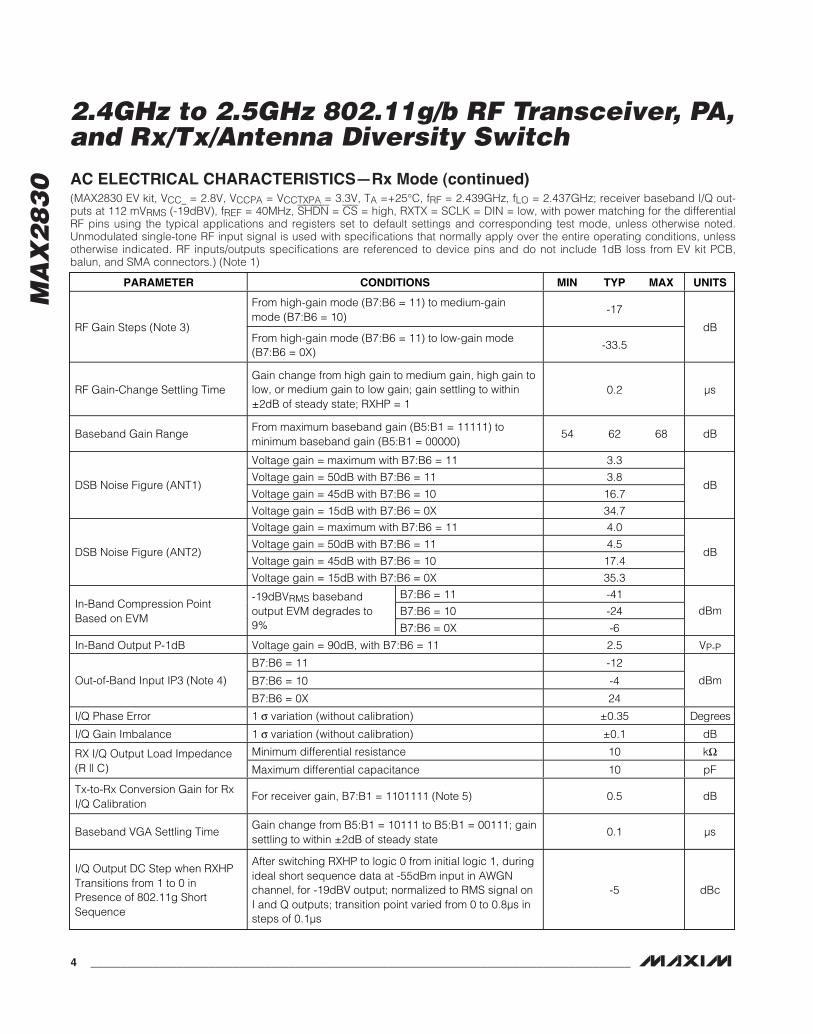
AC ELECTRICAL CHARACTERISTICS—Rx Mode(MAX2830 EV kit, VCC_ = 2.8V, VCCPA = VCCTXPA = 3.3V, TA =+25°C, fRF = 2.439GHz, fLO = 2.437GHz; receiver baseband I/Q out-puts at 112 mVRMS (-19dBV), fREF = 40MHz, SHDN = CS = high, RXTX = SCLK = DIN = low, with power matching for the differentialRF pins using the typical applications and registers set to default settings and corresponding test mode, unless otherwise noted.Unmodulated single-tone RF input signal is used with specifications that normally apply over the entire operating conditions, unlessotherwise indicated. RF inputs/outputs specifications are referenced to device pins and do not include 1dB loss from EV kit PCB,balun, and SMA connectors.) (Note 1)
PARAMETER CONDITIONS MIN TYP MAX UNITS
RECEIVER SECTION: LNA RF INPUT-TO-BASEBAND I/Q OUTPUTS
RF Input Frequency Range 2.4 2.5 GHz
High RF gain 13
Mid RF gain 16RF Input Return Loss (ANT1)
Low RF gain 13
dB
High RF gain 21
Mid RF gain 14RF Input Return Loss (ANT2)
Low RF gain 12
dB
TA = +25°C 86 97Maximum gain, B7:B1 =1111111 TA = -40°C to +85°C 83
Total Voltage Gain (ANT1)Minimum gain, B7:B1 =0000000
TA = +25°C 2 8
dB
Maximum gain, B7:B1 =1111111
TA = +25°C 96
Total Voltage Gain (ANT2)Minimum gain, B7:B1 =0000000
TA = +25°C 2
dB
MA
X2
83
0
2.4GHz to 2.5GHz 802.11g/b RF Transceiver, PA,and Rx/Tx/Antenna Diversity Switch
4 _______________________________________________________________________________________
AC ELECTRICAL CHARACTERISTICS—Rx Mode (continued)(MAX2830 EV kit, VCC_ = 2.8V, VCCPA = VCCTXPA = 3.3V, TA =+25°C, fRF = 2.439GHz, fLO = 2.437GHz; receiver baseband I/Q out-puts at 112 mVRMS (-19dBV), fREF = 40MHz, SHDN = CS = high, RXTX = SCLK = DIN = low, with power matching for the differentialRF pins using the typical applications and registers set to default settings and corresponding test mode, unless otherwise noted.Unmodulated single-tone RF input signal is used with specifications that normally apply over the entire operating conditions, unlessotherwise indicated. RF inputs/outputs specifications are referenced to device pins and do not include 1dB loss from EV kit PCB,balun, and SMA connectors.) (Note 1)
PARAMETER CONDITIONS MIN TYP MAX UNITS
From high-gain mode (B7:B6 = 11) to medium-gainmode (B7:B6 = 10)
-17
RF Gain Steps (Note 3)From high-gain mode (B7:B6 = 11) to low-gain mode(B7:B6 = 0X)
-33.5
dB
RF Gain-Change Settling TimeGain change from high gain to medium gain, high gain tolow, or medium gain to low gain; gain settling to within±2dB of steady state; RXHP = 1
0.2 µs
Baseband Gain RangeFrom maximum baseband gain (B5:B1 = 11111) tominimum baseband gain (B5:B1 = 00000)
54 62 68 dB
Voltage gain = maximum with B7:B6 = 11 3.3
Voltage gain = 50dB with B7:B6 = 11 3.8
Voltage gain = 45dB with B7:B6 = 10 16.7DSB Noise Figure (ANT1)
Voltage gain = 15dB with B7:B6 = 0X 34.7
dB
Voltage gain = maximum with B7:B6 = 11 4.0
Voltage gain = 50dB with B7:B6 = 11 4.5
Voltage gain = 45dB with B7:B6 = 10 17.4DSB Noise Figure (ANT2)
Voltage gain = 15dB with B7:B6 = 0X 35.3
dB
B7:B6 = 11 -41
B7:B6 = 10 -24In-Band Compression PointBased on EVM
-19dBVRMS basebandoutput EVM degrades to9% B7:B6 = 0X -6
dBm
In-Band Output P-1dB Voltage gain = 90dB, with B7:B6 = 11 2.5 VP-P
B7:B6 = 11 -12
B7:B6 = 10 -4Out-of-Band Input IP3 (Note 4)
B7:B6 = 0X 24
dBm
I/Q Phase Error 1 σ variation (without calibration) ±0.35 D eg r ees
I/Q Gain Imbalance 1 σ variation (without calibration) ±0.1 dB
Minimum differential resistance 10 kΩRX I/Q Output Load Impedance(R || C) Maximum differential capacitance 10 pF
Tx-to-Rx Conversion Gain for RxI/Q Calibration
For receiver gain, B7:B1 = 1101111 (Note 5) 0.5 dB
Baseband VGA Settling TimeGain change from B5:B1 = 10111 to B5:B1 = 00111; gainsettling to within ±2dB of steady state
0.1 µs
I/Q Output DC Step when RXHPTransitions from 1 to 0 inPresence of 802.11g ShortSequence
After switching RXHP to logic 0 from initial logic 1, duringideal short sequence data at -55dBm input in AWGNchannel, for -19dBV output; normalized to RMS signal onI and Q outputs; transition point varied from 0 to 0.8µs insteps of 0.1µs
-5 dBc
MA
X2
83
0
2.4GHz to 2.5GHz 802.11g/b RF Transceiver, PA,and Rx/Tx/Antenna Diversity Switch
_______________________________________________________________________________________ 5
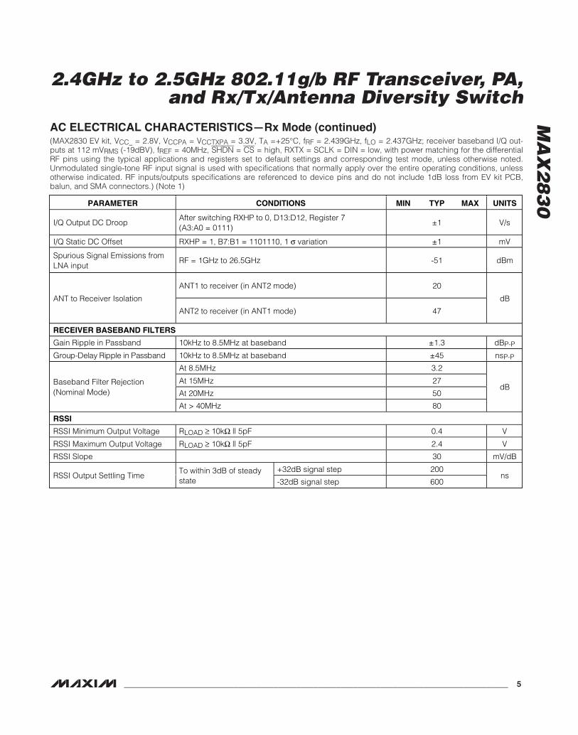
AC ELECTRICAL CHARACTERISTICS—Rx Mode (continued)(MAX2830 EV kit, VCC_ = 2.8V, VCCPA = VCCTXPA = 3.3V, TA =+25°C, fRF = 2.439GHz, fLO = 2.437GHz; receiver baseband I/Q out-puts at 112 mVRMS (-19dBV), fREF = 40MHz, SHDN = CS = high, RXTX = SCLK = DIN = low, with power matching for the differentialRF pins using the typical applications and registers set to default settings and corresponding test mode, unless otherwise noted.Unmodulated single-tone RF input signal is used with specifications that normally apply over the entire operating conditions, unlessotherwise indicated. RF inputs/outputs specifications are referenced to device pins and do not include 1dB loss from EV kit PCB,balun, and SMA connectors.) (Note 1)
PARAMETER CONDITIONS MIN TYP MAX UNITS
I/Q Output DC DroopAfter switching RXHP to 0, D13:D12, Register 7(A3:A0 = 0111)
±1 V/s
I/Q Static DC Offset RXHP = 1, B7:B1 = 1101110, 1 σ variation ±1 mV
Spurious Signal Emissions fromLNA input
RF = 1GHz to 26.5GHz -51 dBm
ANT1 to receiver (in ANT2 mode) 20
ANT to Receiver Isolation
ANT2 to receiver (in ANT1 mode) 47
dB
RECEIVER BASEBAND FILTERS
Gain Ripple in Passband 10kHz to 8.5MHz at baseband ±1.3 dBP-P
G r oup - D el ay Ri p p l e i n P assb and 10kHz to 8.5MHz at baseband ±45 nsP-P
At 8.5MHz 3.2
At 15MHz 27
At 20MHz 50Baseband Filter Rejection(Nominal Mode)
At > 40MHz 80
dB
RSSI
RSSI Minimum Output Voltage RLOAD ≥ 10kΩ || 5pF 0.4 V
RSSI Maximum Output Voltage RLOAD ≥ 10kΩ || 5pF 2.4 V
RSSI Slope 30 mV/dB
+32dB signal step 200RSSI Output Settling Time
To within 3dB of steadystate -32dB signal step 600
ns
MA
X2
83
0
2.4GHz to 2.5GHz 802.11g/b RF Transceiver, PA,and Rx/Tx/Antenna Diversity Switch
6 _______________________________________________________________________________________
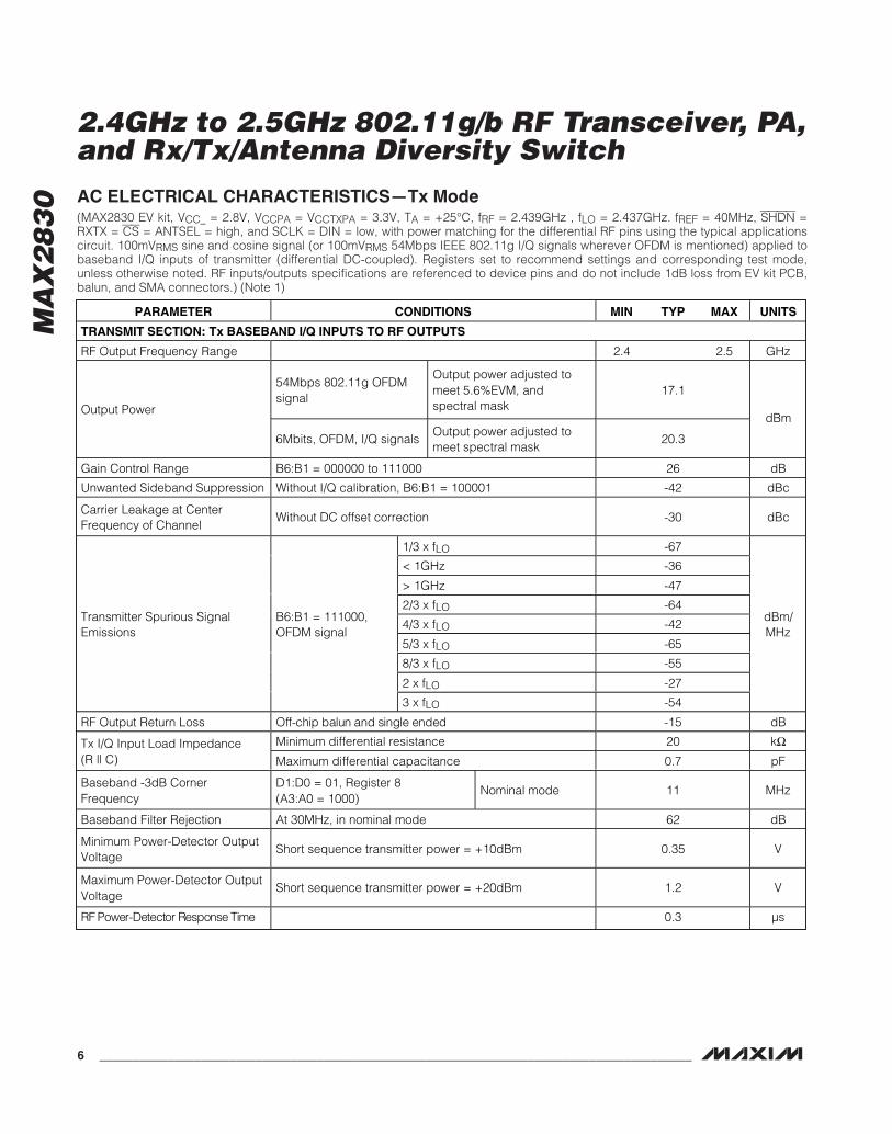
AC ELECTRICAL CHARACTERISTICS—Tx Mode(MAX2830 EV kit, VCC_ = 2.8V, VCCPA = VCCTXPA = 3.3V, TA = +25°C, fRF = 2.439GHz , fLO = 2.437GHz. fREF = 40MHz, SHDN =RXTX = CS = ANTSEL = high, and SCLK = DIN = low, with power matching for the differential RF pins using the typical applicationscircuit. 100mVRMS sine and cosine signal (or 100mVRMS 54Mbps IEEE 802.11g I/Q signals wherever OFDM is mentioned) applied tobaseband I/Q inputs of transmitter (differential DC-coupled). Registers set to recommend settings and corresponding test mode,unless otherwise noted. RF inputs/outputs specifications are referenced to device pins and do not include 1dB loss from EV kit PCB,balun, and SMA connectors.) (Note 1)
PARAMETER CONDITIONS MIN TYP MAX UNITS
TRANSMIT SECTION: Tx BASEBAND I/Q INPUTS TO RF OUTPUTS
RF Output Frequency Range 2.4 2.5 GHz
54Mbps 802.11g OFDMsignal
Output power adjusted tomeet 5.6%EVM, andspectral mask
17.1
Output Power
6Mbits, OFDM, I/Q signalsOutput power adjusted tomeet spectral mask
20.3
dBm
Gain Control Range B6:B1 = 000000 to 111000 26 dB
Unwanted Sideband Suppression Without I/Q calibration, B6:B1 = 100001 -42 dBc
Carrier Leakage at CenterFrequency of Channel
Without DC offset correction -30 dBc
1/3 x fLO -67
< 1GHz -36
> 1GHz -47
2/3 x fLO -64
4/3 x fLO -42
5/3 x fLO -65
8/3 x fLO -55
2 x fLO -27
Transmitter Spurious SignalEmissions
B6:B1 = 111000,OFDM signal
3 x fLO -54
dBm/MHz
RF Output Return Loss O ff- chi p b al un and si ng l e end ed -15 dB
Minimum differential resistance 20 kΩTx I/Q Input Load Impedance(R || C) Maximum differential capacitance 0.7 pF
Baseband -3dB CornerFrequency
D1:D0 = 01, Register 8(A3:A0 = 1000)
Nominal mode 11 MHz
Baseband Filter Rejection At 30MHz, in nominal mode 62 dB
Minimum Power-Detector OutputVoltage
Short sequence transmitter power = +10dBm 0.35 V
Maximum Power-Detector OutputVoltage
Short sequence transmitter power = +20dBm 1.2 V
RF P ow er - D etector Resp onse Ti m e 0.3 µs

MA
X2
83
0
2.4GHz to 2.5GHz 802.11g/b RF Transceiver, PA,and Rx/Tx/Antenna Diversity Switch
_______________________________________________________________________________________ 7
AC ELECTRICAL CHARACTERISTICS—Tx Mode (continued)(MAX2830 EV kit, VCC_ = 2.8V, VCCPA = VCCTXPA = 3.3V, TA = +25°C, fRF = 2.439GHz , fLO = 2.437GHz. fREF = 40MHz, SHDN =RXTX = CS = ANTSEL = high, and SCLK = DIN = low, with power matching for the differential RF pins using the typical applicationscircuit. 100mVRMS sine and cosine signal (or 100mVRMS 54Mbps IEEE 802.11g I/Q signals wherever OFDM is mentioned) applied tobaseband I/Q inputs of transmitter (differential DC-coupled). Registers set to recommend settings and corresponding test mode,unless otherwise noted. RF inputs/outputs specifications are referenced to device pins and do not include 1dB loss from EV kit PCB,balun, and SMA connectors.) (Note 1)
PARAMETER CONDITIONS MIN TYP MAX UNITS
TRANSMITTER LO LEAKAGE AND I/Q CALIBRATION USING LO LEAKAGE AND SIDEBAND DETECTOR(see the Rx/Tx Calibration Mode section)
Tx BASEBAND I/Q INPUTS TO RECEIVER OUTPUTS
Output at 1 x fTONE (for LOleakage = -29dBc),fTONE = 2MHz, 100mVRMS
-34
LO Leakage and SidebandDetector Output
Calibration register,D12:D11 = 00,A3:A0 = 0110 Output at 2 x fTONE (for LO
leakage = -240dBc),fTONE = 2MHz, 100mVRMS
-44
dBVRMS
Amplifier Gain Range D12:D11 = 00 to D12:D11 = 11, A3:A0 = 0110 30 dB
Lower -3dB Corner Frequency 1 MHz
MA
X2
83
0
2.4GHz to 2.5GHz 802.11g/b RF Transceiver, PA,and Rx/Tx/Antenna Diversity Switch
8 _______________________________________________________________________________________
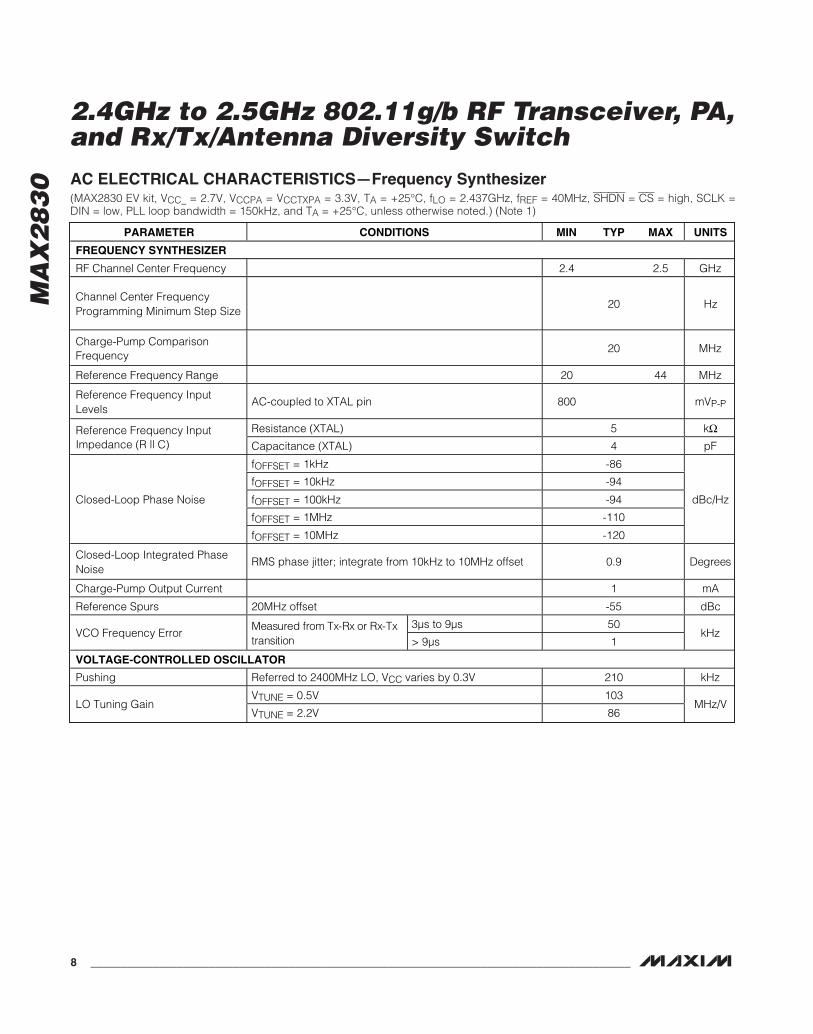
AC ELECTRICAL CHARACTERISTICS—Frequency Synthesizer(MAX2830 EV kit, VCC_ = 2.7V, VCCPA = VCCTXPA = 3.3V, TA = +25°C, fLO = 2.437GHz, fREF = 40MHz, SHDN = CS = high, SCLK =DIN = low, PLL loop bandwidth = 150kHz, and TA = +25°C, unless otherwise noted.) (Note 1)
PARAMETER CONDITIONS MIN TYP MAX UNITS
FREQUENCY SYNTHESIZER
RF Channel Center Frequency 2.4 2.5 GHz
Channel Center FrequencyProgramming Minimum Step Size
20 Hz
Charge-Pump ComparisonFrequency
20 MHz
Reference Frequency Range 20 44 MHz
Reference Frequency InputLevels
AC-coupled to XTAL pin 800 mVP-P
Resistance (XTAL) 5 kΩReference Frequency InputImpedance (R || C) Capacitance (XTAL) 4 pF
fOFFSET = 1kHz -86
fOFFSET = 10kHz -94
fOFFSET = 100kHz -94
fOFFSET = 1MHz -110
Closed-Loop Phase Noise
fOFFSET = 10MHz -120
dBc/Hz
Closed-Loop Integrated PhaseNoise
RMS phase jitter; integrate from 10kHz to 10MHz offset 0.9 D eg r ees
Charge-Pump Output Current 1 mA
Reference Spurs 20MHz offset -55 dBc
3µs to 9µs 50VCO Frequency Error
M easur ed fr om Tx- Rx or Rx- Txtr ansi ti on > 9µs 1
kHz
VOLTAGE-CONTROLLED OSCILLATOR
Pushing Referred to 2400MHz LO, VCC varies by 0.3V 210 kHz
VTUNE = 0.5V 103 LO Tuning Gain VTUNE = 2.2V 86 MHz/V
MA
X2
83
0
2.4GHz to 2.5GHz 802.11g/b RF Transceiver, PA,and Rx/Tx/Antenna Diversity Switch
_______________________________________________________________________________________ 9
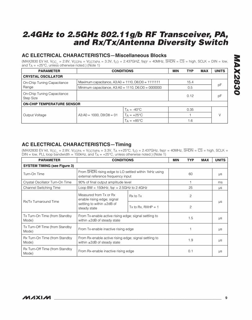
AC ELECTRICAL CHARACTERISTICS—Miscellaneous Blocks(MAX2830 EV kit, VCC_ = 2.8V, VCCPA = VCCTXPA = 3.3V, fLO = 2.437GHZ, fREF = 40MHz, SHDN = CS = high, SCLK = DIN = low,and TA = +25°C, unless otherwise noted.) (Note 1)
PARAMETER CONDITIONS MIN TYP MAX UNITS
CRYSTAL OSCILLATOR
M axi m um cap aci tance, A3:A0 = 1110, D 6:D 0 = 1111111 15.4On-Chip Tuning CapacitanceRange M i ni m um cap aci tance, A3:A0 = 1110, D 6:D 0 = 0000000 0.5
pF
On-Chip Tuning CapacitanceStep Size
0.12 pF
ON-CHIP TEMPERATURE SENSOR
TA = -40°C 0.35
TA = +25°C 1Output Voltage A3:A0 = 1000, D 9:D 8 = 01
TA = +85°C 1.6
V
AC ELECTRICAL CHARACTERISTICS—Timing(MAX2830 EV kit, VCC_ = 2.8V, VCCPA = VCCTXPA = 3.3V, TA =+25°C, fLO = 2.437GHz, fREF = 40MHz, SHDN = CS = high, SCLK =DIN = low, PLL loop bandwidth = 150kHz, and TA = +25°C, unless otherwise noted.) (Note 1)
PARAMETER CONDITIONS MIN TYP MAX UNITS
SYSTEM TIMING (see Figure 3)
Turn-On TimeFrom SHDN rising edge to LO settled within 1kHz usingexternal reference frequency input
60 µs
Crystal Oscillator Turn-On Time 90% of final output amplitude level 1 ms
Channel Switching Time Loop BW = 150kHz, fRF = 2.5GHz to 2.4GHz 25 µs
Rx to Tx 2
Rx/Tx Turnaround Time
Measured from Tx or Rxenable rising edge; signalsettling to within ±2dB ofsteady state Tx to Rx, RXHP = 1 2
µs
Tx Turn-On Time (from StandbyMode)
From Tx-enable active rising edge; signal settling towithin ±2dB of steady state
1.5 µs
Tx Turn-Off Time (from StandbyMode)
From Tx-enable inactive rising edge 1 µs
Rx Turn-On Time (from StandbyMode)
From Rx-enable active rising edge; signal settling towithin ±2dB of steady state
1.9 µs
Rx Turn-Off Time (from StandbyMode)
From Rx-enable inactive rising edge 0.1 µs
MA
X2
83
0
2.4GHz to 2.5GHz 802.11g/b RF Transceiver, PA,and Rx/Tx/Antenna Diversity Switch
10 ______________________________________________________________________________________
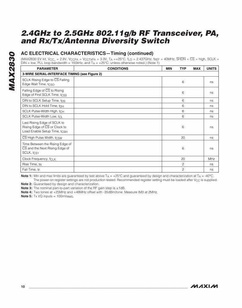
AC ELECTRICAL CHARACTERISTICS—Timing (continued)(MAX2830 EV kit, VCC_ = 2.8V, VCCPA = VCCTXPA = 3.3V, TA =+25°C, fLO = 2.437GHz, fREF = 40MHz, SHDN = CS = high, SCLK =DIN = low, PLL loop bandwidth = 150kHz, and TA = +25°C, unless otherwise noted.) (Note 1)
PARAMETER CONDITIONS MIN TYP MAX UNITS
3-WIRE SERIAL-INTERFACE TIMING (see Figure 2)
SCLK Rising Edge to CS FallingEdge Wait Time, tCSO
6 ns
Falling Edge of CS to RisingEdge of First SCLK Time, tCSS
6 ns
DIN to SCLK Setup Time, tDS 6 ns
DIN to SCLK Hold Time, tDH 6 ns
SCLK Pulse-Width High, tCH 6 ns
SCLK Pulse-Width Low, tCL 6 ns
Last Rising Edge of SCLK toRising Edge of CS or Clock toLoad Enable Setup Time, tCSH
6 ns
CS High Pulse Width, tCSW 20 ns
Time Between the Rising Edge ofCS and the Next Rising Edge ofSCLK, tCS1
6 ns
Clock Frequency, fCLK 20 MHz
Rise Time, tR 2 ns
Fall Time, tF 2 ns
Note 1: Min and max limits are guaranteed by test above TA = +25°C and guaranteed by design and characterization at TA = -40°C.The power-on register settings are not production tested. Recommended register setting must be loaded after VCC is supplied.
Note 2: Guaranteed by design and characterization.Note 3: The nominal part-to-part variation of the RF gain step is ±1dB.Note 4: Two tones at +25MHz and +48MHz offset with -35dBm/tone. Measure IM3 at 2MHz.Note 5: Tx I/Q inputs = 100mVRMS.

MA
X2
83
0
2.4GHz to 2.5GHz 802.11g/b RF Transceiver, PA,and Rx/Tx/Antenna Diversity Switch
______________________________________________________________________________________ 11
Rx ICC vs. VCC
VCC (V)
I CC
(mA)
MAX
2830
toc0
1
2.7 2.8 2.9 3.0 3.1 3.2 3.3 3.4 3.5 3.661
62
63
64
65
66
67
TA = +25°C
TA = -40°C
TA = +85°C
NOISE FIGURE vs. BASEBAND GAIN SETTINGS
GAIN SETTINGS
NF (d
B)
MAX
2830
toc0
2
0 2 4 6 8 10 12 14 16 18 20 22 24 26 28 30 320
5
10
15
20
25
30
35
40
45
LNA = HIGH GAIN
LNA = MEDIUM GAIN
LNA = LOW GAIN
Rx VOLTAGE GAIN vs. BASEBAND GAIN SETTING
GAIN SETTINGS
GAIN
(dB)
MAX
2830
toc0
3
0 2 4 6 8 10 12 14 16 18 20 22 24 26 28 30 320
10
20
30
40
50
60
70
80
90
100
LNA = LOW GAIN
LNA = MEDIUM GAIN
LNA = HIGH GAIN
Rx IN-BAND OUTPUT P - 1dB vs. GAIN
GAIN (dB)
OUTP
UT P
- 1d
B (d
BVRM
S)
MAX
2830
toc0
4
15 25 35 45 55 65 75 85 95-7
-6
-5
-4
-3
-2
-1
0
LNA MEDIUM/HIGH- GAIN SWITCH POINT
LNA MEDIUM/LOW-GAIN SWITCH POINT
Rx EVM vs. PIN
PIN (dBm)
EVM
(%)
MAX
2830
toc0
5
-80 -70 -60 -50 -40 -30 -20 -10 00
2
4
6
8
10
12
14
16
18
20
22LNA = HIGH GAIN LNA = LOW GAIN
LNA = MEDIUM GAIN
Rx EVM vs. VOUT
VOUT (dBVRMS)
EVM
(%)
MAX
2830
toc0
6
-29 -27 -25 -23 -21 -19 -17 -15 -13 -11 -90
0.5
1.0
1.5
2.0
2.5
3.0PIN = -50dBmLNA = HIGH GAIN
OFDM EVM WITH OFDM JAMMER vs. OFFSET FREQUENCY
PJAMMER (dBm)
EVM
(%)
MAX
2830
toc0
7
-65 -55 -45 -35 -250123456789
101112131415
fOFFSET = 20MHz
fOFFSET = 25MHz
fOFFSET = 40MHz
PIN = -62dBm
Rx EMISSION SPECTRUM, LNA INPUTMAX2830 toc08
4/3
LO2
LO 8
/3 L
O
4 LO
16/3
LO
20/3
LO
dBm
-50
-60
-70
-80
-90
-100
-110
-120
-130
-140
-150DC 26.5GHz
LNA INPUT RETURN LOSSvs. RF FREQUENCY (ANT 1)
RF FREQUENCY (MHz)
INPU
T RE
TURN
LOS
S (d
B)
MAX
2830
toc0
9
2300 2400 2500 2600-25
-20
-15
-10
-5
MID GAIN
LOW GAIN
HIGH GAIN
Typical Operating Characteristics(MAX2830 EV kit, VCC_ = 2.8V, VCCPA = VCCTXPA = 3.3V, TA = +25°C, fLO = 2.437GHz, fREF = 40MHz, SHDN = CS = high, RXHP =SCLK = DIN = low.)

MA
X2
83
0
2.4GHz to 2.5GHz 802.11g/b RF Transceiver, PA,and Rx/Tx/Antenna Diversity Switch
12 ______________________________________________________________________________________
Typical Operating Characteristics (continued)(MAX2830 EV kit, VCC_ = 2.8V, VCCPA = VCCTXPA = 3.3V, TA = +25°C, fLO = 2.437GHz, fREF = 40MHz, SHDN = CS = high, RXHP =SCLK = DIN = low.)
LNA INPUT RETURN LOSSvs. RF FREQUENCY (ANT 2)
RF FREQUENCY (MHz)
INPU
T RE
TURN
LOS
S (d
B)
MAX
2830
toc0
9a
2300 2400 25002350 2450 2550 2600-25
-20
-15
-10
-5
MID GAIN
LOW GAIN
HIGH GAIN
Rx RSSI OUTPUT vs. INPUT POWER
PIN (dBm)
RSSI
OUT
PUT
(V)
MAX
2830
toc1
0
-120 -100 -80 -60 -40 -20 0 200
0.5
1.0
1.5
2.0
2.5
3.0
LNA = HIGH GAIN
LNA = MEDIUM GAIN
LNA = LOW GAIN
Rx RSSI STEP RESPONSE (+32dB LNA GAIN STEP)
3V
0
0.45
1.45V
200ns/div
MAX2830 toc11
Rx RSSI STEP RESPONSE (-32dB LNA GAIN STEP)
3V
0V
0V
1.5V
200ns/div
MAX2830 toc12
Rx I/Q DC OFFSET SETTLING RESPONSE (+8dB BB VGA GAIN STEP)
2.0V
5mV
40ns/div
10mV
0V
0V
MAX2830 toc13
Rx I/Q DC OFFSET SETTLING RESPONSE (-8dB BB VGA GAIN STEP)
MAX2830 toc14
2.5V
5mV
40ns/div
10mV
0V
0mV
Rx I/Q DC OFFSET SETTLING RESPONSE (-16dB BB VGA GAIN STEP)
3VMAX2830 toc15
5mV
400ns/div
10mV
0V
0V
Rx I/Q DC OFFSET SETTLING RESPONSE (-32dB BB VGA GAIN STEP)
3VMAX2830 toc16
5mV
400ns/div
10mV
0V
0V
I/Q OUTPUT DC ERROR DROOP (RxHP = 1→0; 100Hz MODE)
3VMAX2830 toc17
-5mV
20ms/div
0V
0V
-10mV

MA
X2
83
0
2.4GHz to 2.5GHz 802.11g/b RF Transceiver, PA,and Rx/Tx/Antenna Diversity Switch
______________________________________________________________________________________ 13
Rx BB VGA SETTLING RESPONSE (+8 GAIN STEP)
500mV
-500mV
3V
0V
0V
MAX2830 toc18
40ns/div
Rx BB VGA SETTLING RESPONSE (-8 GAIN STEP)
3V
0V
MAX2830 toc19
500mV
-500mV
0V
40ns/div
Rx BB VGA SETTLING RESPONSE (-16 GAIN STEP)
MAX2830 toc20
500mV
-500mV
3V
0V
0V
40ns/div
Rx BB VGA SETTLING RESPONSE (-32 GAIN STEP)
MAX2830 toc21
500mV
-500mV
3V
0V
0V
40ns/div
RF LNA SETTLING RESPONSE (HIGH TO MEDIUM)
MAX2830 toc22
500mV
-500mV
3V
0V
0V
100ns/div
RF LNA SETTLING RESPONSE (HIGH TO LOW)
MAX2830 toc23
500mV
-500mV
3V
0V
0V
100ns/div
Rx BB FREQUENCY RESPONSEvs. FINE SETTING (COARSE SETTING = 8.5MHz)
FREQUENCY (MHz)
dB
MAX
2830
toc2
4
-100
-80
-60
-40
-20
0
20
1 10 100
Rx BB FREQUENCY RESPONSEvs. COARSE SETTING (FINE SETTING = 010)
FREQUENCY (MHz)
dB
MAX
2830
toc2
5
-120
-100
-80
-60
-40
-20
0
20
1 10 100
Rx BASEBAND FILTERGROUP DELAY
MAX2830 toc26
FREQUENCY (MHz)
20ns
/div
121
Typical Operating Characteristics (continued)(MAX2830 EV kit, VCC_ = 2.8V, VCCPA = VCCTXPA = 3.3V, TA = +25°C, fLO = 2.437GHz, fREF = 40MHz, SHDN = CS = high, RXHP =SCLK = DIN = low.)

MA
X2
83
0
2.4GHz to 2.5GHz 802.11g/b RF Transceiver, PA,and Rx/Tx/Antenna Diversity Switch
14 ______________________________________________________________________________________
0
38
19
76
57
95
114HISTOGRAM: Rx PHASE IMBALANCE
MAX
2830
toc2
9
1σ/div
MEAN: 0.3°STD: 0.314°SAMPLE SIZE: 1013
Tx ICC vs. VCC
VCC (V)
I CC
(mA)
MAX
2830
toc3
0
2.7 2.8 2.9 3.0 3.1 3.2 3.3 3.4 3.5 3.678
80
82
84
86
88
TA = +25°C
TA = -40°C
TA = +85°C
0
16
8
32
24
40
48HISTOGRAM: Tx LO LEAKAGE
MAX
2830
toc3
1
1σ/div
MEAN: -33.45dBcSTD: 6.31dBSAMPLE SIZE: 999
0
26
13
52
39
65
78HISTOGRAM: Rx STATIC DC OFFSET
MAX
2830
toc2
7
1σ/div
MEAN: 0mVSTD: 0.977mVSAMPLE SIZE: 1006
0
46
23
92
69
115
138HISTOGRAM: Rx GAIN IMBALANCE
MAX
2830
toc2
8
1σ/div
MEAN: 0dBSTD: 0.064dBSAMPLE SIZE: 951
0
24
12
48
36
60
72
HISTOGRAM: Tx SIDEBANDSUPPRESSION
MAX
2830
toc3
2
1σ/div
MEAN: -42dBcSTD: 1.9dBSAMPLE SIZE: 1000
-90
-70
-60
-50
-40
-30
-20
-10
0
0.1 1 10 100
Tx BASEBAND FILTER RESPONSE
MAX
2830
toc3
3
BASEBAND FREQUENCY (MHz)
FILT
ER R
ESPO
NSE
(dB)
-80
Tx EVM vs. POUT
POUT (dBm)
EVM
(%)
MAX
2830
toc3
4
0 5 10 15 20 250
2
4
6
8
10
12
14
16
18
VCC = 4.2V
VCC = 3.3V
VCC = 3V
VCC = 2.7V
Typical Operating Characteristics (continued)(MAX2830 EV kit, VCC_ = 2.8V, VCCPA = VCCTXPA = 3.3V, TA = +25°C, fLO = 2.437GHz, fREF = 40MHz, SHDN = CS = high, RXHP =SCLK = DIN = low.)
PA SUPPLY CURRENT vs. POUT
POUT (dBm)
PA S
UPPL
Y CU
RREN
T (m
A)
MAX
2830
toc3
5
0 5 10 15 20 25120
150
180
210
240
270
300
330
360
VCCPA = 4.2V
VCCPA = 2.7V, 3.0V, 3.3V
MA
X2
83
0
POWER DETECTOR OVER FREQUENCY
POUT (dBm)
POW
ER D
ETEC
TOR
(V)
MAX
2830
toc4
0
0 5 10 15 20 250
0.5
1.0
1.5
2.0
2.5
fRF = 2.4GHz
fRF = 2.5GHz
POWER DETECTOR OVER SUPPLY VOLTAGE
POUT (dBm)
POW
ER D
ETEC
TOR
(V)
MAX
2830
toc4
1
0 5 10 15 20 250
0.5
1.0
1.5
2.0
VCCPA = 2.7V, 3.0V
VCCPA = 3.3V, 4.2V
POWER DETECTOR OVER TEMPERATURE
POUT (dBm)
POW
ER D
ETEC
TOR
(V)
MAX
2830
toc4
2
0 5 10 15 20 250
0.5
1.0
1.5
2.0
2.5
TA = +85°C
TA = +25°C,-40°C
POWER-DETECTOR OUTPUT
100ns/div
MAX
2830
toc4
3
300mV
-300mV
0V
1V
20dB GAIN STEP PA ENVELOPE
POWER DETECTOR
2.4GHz to 2.5GHz 802.11g/b RF Transceiver, PA,and Rx/Tx/Antenna Diversity Switch
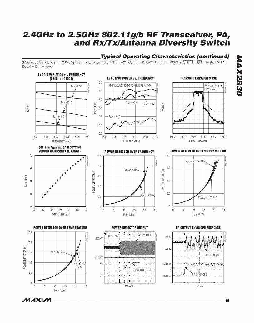
______________________________________________________________________________________ 15
TRANSMIT EMISSION MASK
MAX
2830
toc3
8
FREQUENCY/MHz
10dB
/div
246724472407 24272387 2487
POUT = +17.1dBm EVM = 5.6%
802.11g POUT vs. GAIN SETTING (UPPER GAIN CONTROL RANGE)
GAIN SETTINGS
P OUT
(dBm
)
MAX
2830
toc3
9
40 44 48 52 56 60 6414
16
18
20
22
Typical Operating Characteristics (continued)(MAX2830 EV kit, VCC_ = 2.8V, VCCPA = VCCTXPA = 3.3V, TA = +25°C, fLO = 2.437GHz, fREF = 40MHz, SHDN = CS = high, RXHP =SCLK = DIN = low.)
Tx GAIN VARIATION vs. FREQUENCY(B6:B1 = 101001)
FREQUENCY (GHz)
2dB/
div
MAX
2830
toc3
6
2.4 2.42 2.44 2.46 2.48 2.5
TA = -40°C
TA = +25°C
TA = +85°C
PA OUTPUT ENVELOPE RESPONSE
1µs/div
MAX
2830
toc4
4
-20dBm
0
20dBm
-50mV
50mV
PA ENVELOPE
TX I/Q INPUT
Tx OUTPUT POWER vs. FREQUENCY
FREQUENCY (GHz)
P OUT
(dBm
)
MAX
2830
toc3
7
2.40 2.42 2.44 2.46 2.48 2.5015.0
15.5
16.0
16.5
17.0
17.5
18.0
TA = -40°C
TA = +25°CTA = +85°C
GAIN ADJUSTED TO ACHIEVE 5.6% EVM
MA
X2
83
0
2.4GHz to 2.5GHz 802.11g/b RF Transceiver, PA,and Rx/Tx/Antenna Diversity Switch
16 ______________________________________________________________________________________
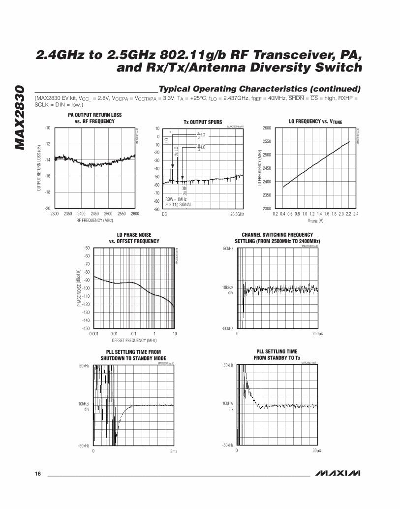
PA OUTPUT RETURN LOSSvs. RF FREQUENCY
RF FREQUENCY (MHz)
OUTP
UT R
ETUR
N LO
SS (d
B)
MAX
2830
toc4
5
2300 2350 2400 2450 2500 2550 2600-20
-18
-16
-14
-12
-10Tx OUTPUT SPURS
MAX2830 toc46
0
-80
-90
10
-70
-60
-50
-40
-30
-20
-10
26.5GHzDC
LO
2x L
O
3x R
F
RBW = 1MHz 802.11g SIGNAL
43 LO
83 LO
PLL SETTLING TIME FROMSHUTDOWN TO STANDBY MODE
50kHz
-50kHz0 2ms
10kHz/div
MAX2830 toc50
CHANNEL SWITCHING FREQUENCY SETTLING (FROM 2500MHz TO 2400MHz)
50kHz
-50kHz250µs0
10kHz/div
MAX2830 toc49
LO PHASE NOISEvs. OFFSET FREQUENCY
OFFSET FREQUENCY (MHz)
PHAS
E NO
ISE
(dBc
/Hz)
MAX
2830
toc4
8
-150
-140
-130
-120
-110
-100
-90
-80
-70
-60
-50
0.001 0.01 0.1 1 10
LO FREQUENCY vs. VTUNE
VTUNE (V)
LO F
REQU
ENCY
(MHz
)
MAX
2830
toc4
7
0.2 0.4 0.6 0.8 1.0 1.2 1.4 1.6 1.8 2.0 2.2 2.42300
2350
2400
2450
2500
2550
2600
Typical Operating Characteristics (continued)(MAX2830 EV kit, VCC_ = 2.8V, VCCPA = VCCTXPA = 3.3V, TA = +25°C, fLO = 2.437GHz, fREF = 40MHz, SHDN = CS = high, RXHP =SCLK = DIN = low.)
PLL SETTLING TIME FROM STANDBY TO Tx
50kHz
-50kHz0 30µs
10kHz/div
MAX2830 toc51
MA
X2
83
0
2.4GHz to 2.5GHz 802.11g/b RF Transceiver, PA,and Rx/Tx/Antenna Diversity Switch
______________________________________________________________________________________ 17
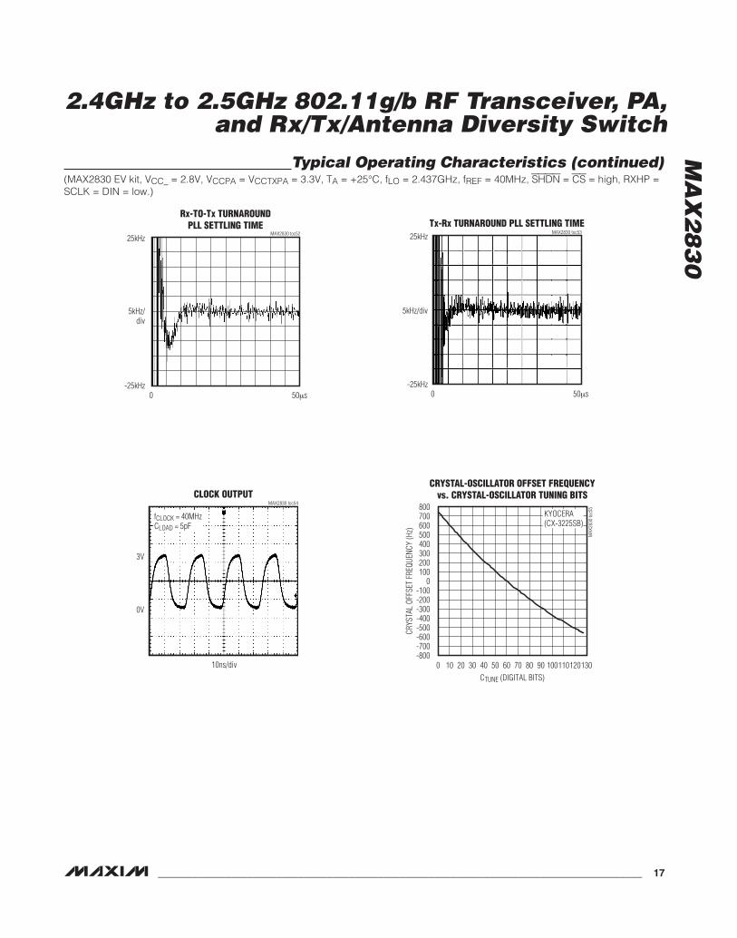
Rx-TO-Tx TURNAROUNDPLL SETTLING TIME
25kHz
-25kHz50µs0
5kHz/div
MAX2830 toc52
Tx-Rx TURNAROUND PLL SETTLING TIME
5kHz/div
-25kHz0 50µs
25kHzMAX2830 toc53
Typical Operating Characteristics (continued)(MAX2830 EV kit, VCC_ = 2.8V, VCCPA = VCCTXPA = 3.3V, TA = +25°C, fLO = 2.437GHz, fREF = 40MHz, SHDN = CS = high, RXHP =SCLK = DIN = low.)
CLOCK OUTPUT
0V
10ns/div
3V
MAX2830 toc54
fCLOCK = 40MHzCLOAD = 5pF
CRYSTAL-OSCILLATOR OFFSET FREQUENCY vs. CRYSTAL-OSCILLATOR TUNING BITS
CTUNE (DIGITAL BITS)
CRYS
TAL
OFFS
ET F
REQU
ENCY
(Hz)
MAX
2830
toc5
5
0 10 20 30 40 50 60 70 80 90 100110120130-800-700-600-500-400-300-200-100
0100200300400500600700800
KYOCERA (CX-3225SB)

MA
X2
83
0
2.4GHz to 2.5GHz 802.11g/b RF Transceiver, PA,and Rx/Tx/Antenna Diversity Switch
18 ______________________________________________________________________________________
B2
1
2
3
4
5
6
7
8
9
10
11
12
13 14 15 16 17 18 19 20 21 22 23 24
48 47 46 45 44 43 42 41 40 39 38 37
36
35
34
33
32
31
30
29
28
27
26
25
VCCLNA
B6
GNDRXLNA
ANT1+
ANT1-
B7
VCCPA
ANT2+
ANT2-
SHDN
POWER DETECTORSERIAL
INTERFACE
TEMPSENSOR
AMDETECTOR
V CCT
XPA B5 CS
RSSI
V CCT
XMX
SCLK DIN
V CCP
LL
CLOC
KOUT LD B1
CPOU
T
RXBBQ+
RXBBQ-RX QOUTPUTS
RX/TX GAINCONTROL
B4
BYPASS
TUNE
GNDVCO
CTUNE
VCCVCO
XTAL
PLL
%1,2
%1,2
GNDCP
SERIAL INPUTS
VCCXTAL
VCCCP
RXTX
ANTS
EL
V CCR
XMX
TXBB
I+
TXBB
I-
TXBB
Q+
TXBB
Q-
V CCR
XFL
RXHP
V CCR
XVGA
RXBB
I+
RXBB
I-
MAX2830
MODECONTROL
RX/TX GAINCONTROL
RX/TX GAINCONTROL
REFERENCECLOCK BUFFER
OUTPUT
NOTE: ALL GROUND PINS (PINS 2, 26, AND 31) AND BYPASS CAPACITORS’ GROUND REQUIRE THEIR OWN VIAS TO GROUND.DO NOT CONNECT THEM TO THE EXPOSED PADDLE GROUND.
RX BASEBAND HPFCORNER FREQUENCY
CONTROL
B3
RX/TXGAIN CONTROL
RX INPUT
TX OUTPUT
MODE CONTROL
RX/TX GAINCONTROL
RX/TX GAINCONTROL
RX GAINCONTROL
TX INPUT RX I OUTPUTS
0°
90°
RSSIMUX
TO RSSIMUX
RSSI
TEMPSENSOR
CRYSTALOSCILLATOR/
BUFFER
RSSITORSSIMUX
MUX
IMUX QMUX
MUX
Rx/T
x ANT
ENNA
SW
ITCH
Block Diagram/Typical Operating Circuit
MA
X2
83
0
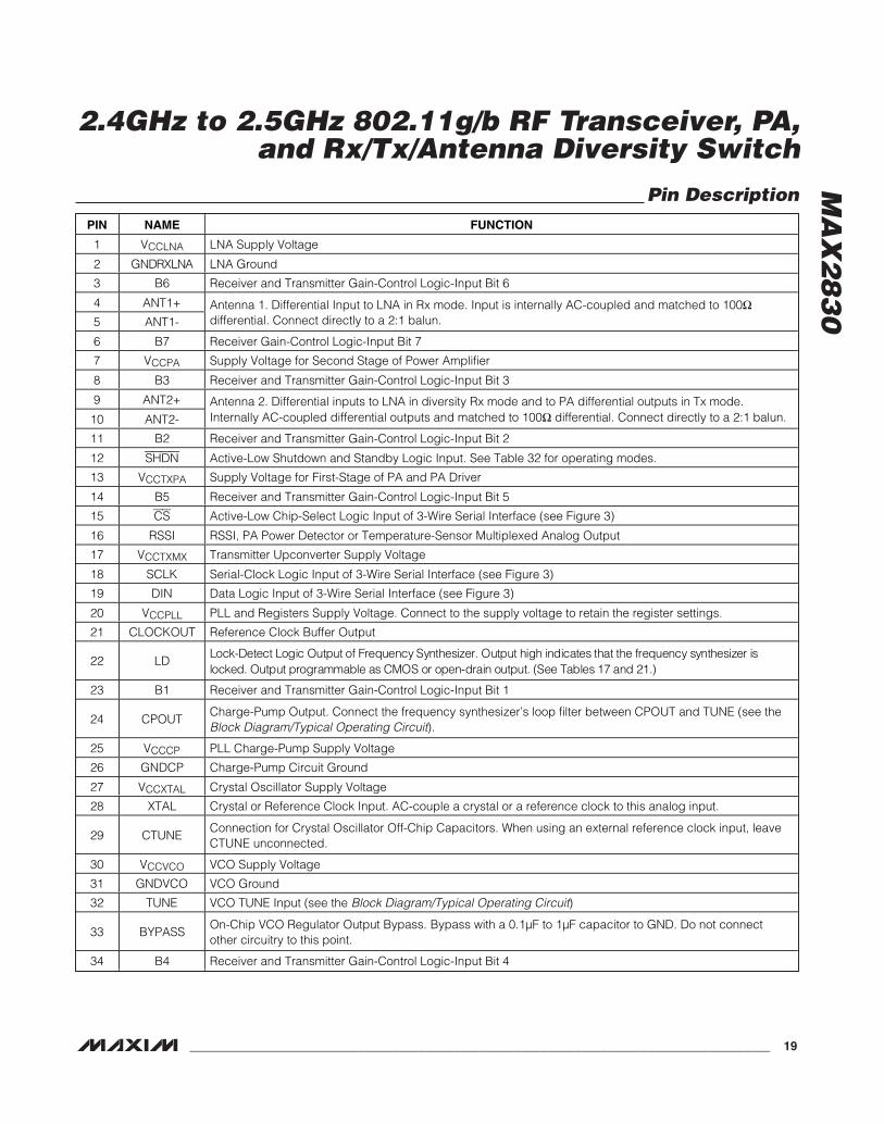
Pin DescriptionPIN NAME FUNCTION
1 VCCLNA LNA Supply Voltage
2 GN DRX LNA LNA Ground
3 B6 Receiver and Transmitter Gain-Control Logic-Input Bit 6
4 ANT1+
5 ANT1-Antenna 1. Differential Input to LNA in Rx mode. Input is internally AC-coupled and matched to 100Ωdifferential. Connect directly to a 2:1 balun.
6 B7 Receiver Gain-Control Logic-Input Bit 7
7 VCCPA Supply Voltage for Second Stage of Power Amplifier
8 B3 Receiver and Transmitter Gain-Control Logic-Input Bit 3
9 ANT2+
10 ANT2-Antenna 2. Differential inputs to LNA in diversity Rx mode and to PA differential outputs in Tx mode.Internally AC-coupled differential outputs and matched to 100Ω differential. Connect directly to a 2:1 balun.
11 B2 Receiver and Transmitter Gain-Control Logic-Input Bit 2
12 SHDN Active-Low Shutdown and Standby Logic Input. See Table 32 for operating modes.
13 VCCTXPA Supply Voltage for First-Stage of PA and PA Driver
14 B5 Receiver and Transmitter Gain-Control Logic-Input Bit 5
15 CS Active-Low Chip-Select Logic Input of 3-Wire Serial Interface (see Figure 3)
16 RSSI RSSI, PA Power Detector or Temperature-Sensor Multiplexed Analog Output
17 VCCTXMX Transmitter Upconverter Supply Voltage
18 SCLK Serial-Clock Logic Input of 3-Wire Serial Interface (see Figure 3)
19 DIN Data Logic Input of 3-Wire Serial Interface (see Figure 3)
20 VCCPLL PLL and Registers Supply Voltage. Connect to the supply voltage to retain the register settings.
21 CLOCKOUT Reference Clock Buffer Output
22 LDLock- D etect Log i c Outp ut of Fr eq uency S ynthesi zer . O utp ut hi g h i nd i cates that the fr eq uency synthesi zer i sl ocked . Outp ut p r og r am m ab l e as C M O S or op en- d r ai n outp ut. ( S ee Tab l es 17 and 21.)
23 B1 Receiver and Transmitter Gain-Control Logic-Input Bit 1
24 CPOUTCharge-Pump Output. Connect the frequency synthesizer’s loop filter between CPOUT and TUNE (see theBlock Diagram/Typical Operating Circuit).
25 VCCCP PLL Charge-Pump Supply Voltage
26 GNDCP Charge-Pump Circuit Ground
27 VCCXTAL Crystal Oscillator Supply Voltage
28 XTAL Crystal or Reference Clock Input. AC-couple a crystal or a reference clock to this analog input.
29 CTUNEConnection for Crystal Oscillator Off-Chip Capacitors. When using an external reference clock input, leaveCTUNE unconnected.
30 VCCVCO VCO Supply Voltage
31 GNDVCO VCO Ground
32 TUNE VCO TUNE Input (see the Block Diagram/Typical Operating Circuit)
33 BYPASSOn-Chip VCO Regulator Output Bypass. Bypass with a 0.1µF to 1µF capacitor to GND. Do not connectother circuitry to this point.
34 B4 Receiver and Transmitter Gain-Control Logic-Input Bit 4
2.4GHz to 2.5GHz 802.11g/b RF Transceiver, PA,and Rx/Tx/Antenna Diversity Switch
______________________________________________________________________________________ 19

MA
X2
83
0
2.4GHz to 2.5GHz 802.11g/b RF Transceiver, PA,and Rx/Tx/Antenna Diversity Switch
20 ______________________________________________________________________________________
Detailed DescriptionThe MAX2830 single-chip, low-power, direct conversion,zero-IF transceiver is designed to support 802.11g/bapplications operating in the 2.4GHz to 2.5GHz band.The fully integrated transceivers include a receive path,transmit path, VCO, sigma-delta fractional-N synthesizer,crystal oscillator, RSSI, PA power detector, temperaturesensor, Rx and Tx I/Q error-detection circuitry, baseband-control interface, linear power amplifier, and an Rx/Txantenna diversity switch. The only additional componentsrequired to implement a complete radio front-end solutionare a crystal, a pair of baluns, a BPF, and a small numberof passive components (RCs, no inductors required).
Rx/Tx and Antenna Diversity SwitchesThe MAX2830 integrates an Rx/Tx switch and an anten-na diversity switch before the receiver and after thepower amplifier. See Figure 1 for a block diagram of theswitches. The receiver and transmitter enable pin(RXTX) and the antenna selection pin (ANTSEL) deter-mine which ports (ANT1 or ANT2) the receiver or trans-mitter is connected to. See Table 1 for the Rx/Tx andantenna diversity switches truth table. When RXTX = 0
(receive mode) and ANTSEL = 0, the switch provides alow-insertion loss path (main) between the ANT1 port(pins 4 and 5) and the receiver. When RXTX = 0(receive mode) and ANTSEL = 1, the switch provides
Pin Description (continued)PIN NAME FUNCTION
35 RXBBQ-
36 RXBBQ+Receiver Baseband Q-Channel Differential Outputs. In TX calibration mode, these pins are the LO leakageand sideband detector outputs.
37 RXBBI-
38 RXBBI+Receiver Baseband I-Channel Differential Outputs. In TX calibration mode, these pins are the LO leakageand sideband detector outputs.
39 VCCRXVGA Receiver VGA Supply Voltage
40 RXHP Receiver Baseband AC-Coupling High-Pass Corner Frequency Control Logic Input
41 VCCRXFL Receiver Baseband Filter Supply Voltage
42 TXBBQ-
43 TXBBQ+Transmitter Baseband I-Channel Differential Inputs
44 TXBBI-
45 TXBBI+Transmitter Baseband Q-Channel Differential Inputs
46 VCCRXMX Receiver Downconverters Supply Voltage
47 ANTSEL Antenna Selection Logic Input. See Table 1 for operation
48 RXTX Rx/Tx Mode Control Logic Input. See Table 32 for operating modes.
— EPExposed Paddle. Connect to the ground plane with multiple vias for proper operation and heat dissipation.Do not share with any other pin grounds and bypass capacitors' ground.
Table 1. Rx/Tx and Antenna Diversity Switches OperationRXTX ANTSEL MODE ANTENNA
0 0 Rx (main) Ant1_0 1 Rx (diversity) Ant2_1 X Tx Ant2_
MAX2830
2
2
ANT1
2
2
LNA
PA
2
ANT2
Figure 1. Simplified Rx/Tx and Antenna Diversity Switch Structure

MA
X2
83
0
2.4GHz to 2.5GHz 802.11g/b RF Transceiver, PA,and Rx/Tx/Antenna Diversity Switch
______________________________________________________________________________________ 21
an antenna diversity path between the ANT2 port (pins9 and 10) and the receiver. When RXTX = 1, the PAand transmit path are automatically connected to theANT2 port, regardless of the logic state of ANTSEL. Forsolutions not requiring antenna diversity, set ANTSELlogic-level high, enabling only the ANT2 port for bothreceive and transmit modes.
The ANT1 and ANT2 differential ports are internally AC-coupled and internally matched to 100Ω. Directly con-nect 2:1 baluns or balanced bandpass filters (BPFs) tothese ports for applications requiring antenna diversity.For applications not requiring antenna diversity, only asingle balun or balanced BPF is required on the ANT2port, and the ANT1 port can be left open. Provide elec-trically symmetrical input traces to the baluns to main-tain IP2 and RF common-mode noise rejection for thereceiver, and to maintain a balanced load for the PA.
ReceiverAfter the switch, the receiver integrates an LNA and VGAwith a 95dB digitally programmable gain control range,direct-conversion downconverters, I/Q baseband low-pass filters with programmable LPF corner frequencies,analog RSSI and integrated DC-offset correction circuitry.A logic-low on the RXTX input (pin 48) and a logic-high onthe SHDN input (pin 12) enable the receiver.
LNA Gain ControlThe LNA has three gain modes: max gain, max gain -16dB, and max gain -33dB. The three LNA gainmodes can be serially programmed through the SPI™
interface by programming bits D6:D5 in Register 11(A3:A0 = 1011) or programmed in parallel through thedigital logic gain-control pins, B7 (pin 6) and B6 (pin 3).Set bit D12 = 1 in Register 8 (A3:A0 = 1000) to enableprogramming through the SPI interface, or set bit D12 =0 to enable parallel programming. See Table 2 for LNAgain-control settings.
Baseband Variable-Gain AmplifierThe receiver baseband variable-gain amplifiers provide62dB of gain control range programmable in 2dB steps.The VGA gain can be serially programmed through theSPI interface by setting bits D4:D0 in Register 11 (A3:A0= 1011) or programmed in parallel through the digitallogic gain-control pins, B5 (pin 14), B4 (pin 34), B3 (pin8), B2 (pin 11), and B1 (pin 23). Set bit D12 = 1 inRegister 8 (A3:A0 = 1000) to enable serial programmingthrough the serial interface or set bit D12 = 0 to enableparallel programming through the external logic pins.See Table 3 for the gain-step value and Table 4 forbaseband VGA gain-control settings.
Receiver Baseband Lowpass FilterThe receiver integrates lowpass filters that provide anupper -3dB corner frequency of 8.5MHz (nominal mode)with 50dB of attenuation at 20MHz, and 45ns of groupdelay ripple in the passband (10kHz to 8.5MHz). Theupper -3dB corner frequency is tightly controlled on-chipand does not require user adjustment. However, provi-sions are made to allow fine tuning of the upper -3dB
Table 3. Receiver Baseband VGA Gain-Step Value (Pins B5:B1 or Register D4:D0,A3:A0 = 1011)
Table 4. Baseband VGA Gain-ControlSettings in Receiver Gain-Control Register(Pin B5:B1 or Register D4:D0, A3:A0 = 1011)
Table 5. Receiver LPF Coarse -3dBCorner Frequency Settings in Register(A3:A0 = 1000)PIN/BIT GAIN STEP (dB)
B1/D0 2
B2/D1 4
B3/D2 8
B4/D3 16
B5/D4 32
B5:B1 OR D4:D0 GAIN
11111 Max
11110 Max - 2dB
11101 Max - 4dB
: :
00000 Min
BITS (D1:D0)-3dB CORNER
FREQUENCY (MHz)MODE
00 7.5 11b01 8.5 11g
10 15 Turbo 1
11 18 Turbo 2
Table 2. LNA Gain-Control Settings (PinsB7:B6 or Register A3:A0 = 1011, D6:D5)B7 OR D6 B6 OR D5 NAME DESCRIPTION
1 1 High Max gain
1 0 Medium Max gain - 16dB (typ)
0 X Low Max gain - 33dB (typ)
SPI is a trademark of Motorola, Inc.

MA
X2
83
0
2.4GHz to 2.5GHz 802.11g/b RF Transceiver, PA,and Rx/Tx/Antenna Diversity Switch
22 ______________________________________________________________________________________
corner frequency. In addition, coarse frequency tuningallows the -3dB corner frequency to be set to 7.5MHz(11b mode), 8.5MHz (11g mode), 15MHz (turbo 1 mode),and 18MHz (turbo 2 mode) by programming bits D1:D0in Register 8 (A3:A0 = 1000). See Table 3. The coarsecorner frequency can be fine-tuned approximately ±10%in 5% steps by programming bits D2:D0 in Register 7(A3:A0 = 0111). See Table 6 for receiver LPF fine -3dBcorner frequency adjustment.
Baseband Highpass Filter and DC Offset Correction
The receiver implements programmable AC and near-DC coupling of I/Q baseband signals. Temporary AC-coupling is used to quickly remove LO leakage andother DC offsets that could saturate the receiver out-puts. When DC offsets have settled, near DC-couplingis enabled to avoid attenuation of the received signal.AC-coupling is set (-3dB highpass corner frequency of600kHz) when a logic-high is applied to RXHP (pin 40).Near DC-coupling is set (-3dB highpass corner fre-quency of 100Hz nominal) when a logic-low is appliedto RXHP. Bits D13:D12 in Register 7 (A3:A0 = 0111)allow the near DC-coupling -3B highpass corner fre-quency to be set to 100Hz (D13:D12 = 00), 4kHz(D13:D12 = X1), or 30kHz (D13:D12 = 10). See Table 7.
Receiver I/Q Baseband OutputsThe differential outputs (RXBBI+, RXBBI-, RXBBQ+,RXBBQ-) of the baseband amplifiers have a differentialoutput impedance of ~300Ω, and are capable of dri-ving differential loads up to 10kΩ || 10pF. The outputsare internally biased to a common-mode voltage of1.2V and are intended to be DC-coupled to the in-phase (I) and quadrature (Q) analog-to-digital dataconverter inputs of the accompanying baseband IC.Additionally, the common-mode output voltage can beadjusted from 1.2V to 1.5V through programming bitsD11:D10 in Register 15 (A3:A0 = 1111).
Received Signal-Strength Indicator (RSSI)The RSSI output (pin 16) can be programmed to multi-plex an analog output voltage proportional to thereceived signal strength, the PA output power, or thedie temperature. Set bits D9:D8 = 00 in Register 8(A3:A0 = 1000) to enable the RSSI output in receivemode (off in transmit mode). Set bit D10 = 1 to enablethe RSSI output when RXHP = 1, and disable the RSSIoutput when RXHP = 0. Set bit D10 = 0 to enable theRSSI output independent of RXHP. See Table 8 for asummary of the RSSI output vs. register programmingand RXHP.
The RSSI provides an analog voltage proportional tothe log of the sum of the squares of the I and Q chan-nels, measured after the receive baseband filters andbefore the variable-gain amplifiers. The RSSI analogoutput voltage is proportional to the RF input signallevel and LNA gain state over a 60dB range, and is notdependent upon VGA gain. See the Rx RSSI Output vs.Input Power graph in the Typical OperatingCharacteristics for further details.
Table 8. RSSI Pin Truth TableINPUT CONDITIONS
A3:A0 = 1000,D9:D8
A3:A0 = 1000,D10
RXHPRSSI OUTPUT
X 0 0 No signal
00 0 1 RSSI
01 0 1Temperature
sensor
10 0 1 Power detector
00 1 X RSSI
01 1 XTemperature
sensor
10 1 X Power detector
Table 6. Receiver LPF Fine -3dB CornerFrequency Adjustment in Register (A3:A0 = 0111)
BITS (D2:D0)% ADJUSTMENT RELATIVE TO
COARSE SETTING
000 90
001 95
010 100
011 105
100 110
Table 7. Receiver Highpass Filter -3dBCorner Frequency Programming
RXHP A3:A0 = 0111,
D13:D12-3dB HIGHPASS CORNER
FREQUENCY (Hz)
1 XX 600k
0 00 100 (recommended)
0 X1 4k
0 10 30k
X = Don’t care. X = Don’t care.

MA
X2
83
0
2.4GHz to 2.5GHz 802.11g/b RF Transceiver, PA,and Rx/Tx/Antenna Diversity Switch
______________________________________________________________________________________ 23
TransmitterThe transmitter integrates baseband lowpass filters,direct-upconversion mixers, a VGA, a PA driver, and a lin-ear RF PA with a power detector. A logic-high on theRXTX input (pin 48) and a logic-high on the SHDN input(pin 12) enable the transmitter. The PA outputs are routedto ANT2, regardless of the state at ANTSEL.
Transmitter I/Q Baseband InputsThe differential analog inputs of the transmitter basebandamplifier I/Q inputs (TXBBI+, TXBBI-, TXBBQ+, TXBBQ-)have a differential impedance of 20kΩ || 1pF. The inputsrequire an input common-mode voltage of 0.9V to 1.3V,which is provided by the DC-coupled I and Q DAC out-puts of the accompanying baseband IC.
Transmitter Baseband Lowpass FilteringThe transmitter integrates lowpass filters that can betuned to -3dB corner frequencies of 8MHz (11b),11MHz (11g), 16.5MHz (turbo 1 mode), and 22.5MHz(turbo 2 mode) through programming bits D1:D0 in
Register 8 (A3:A0 = 1000) and bit D5:D3 in Register 7(A3:A0 = 0111). The -3dB corner frequency is tightlycontrolled on-chip and does not require user adjust-ment. Additionally, provisions are made to fine tune the-3dB corner frequency through bits D5:D3 in the FilterProgramming register (A3:A0 = 0111). See Tables 9and 10.
Transmitter Variable-Gain AmplifierThe variable-gain amplifier of the transmitter provides31dB of gain control range programmable in 0.5dBsteps over the top 8dB of the gain control range and in1dB steps below that. The transmitter gain can be pro-grammed serially through the SPI interface by settingbits D5:D0 in Register 12 (A3:A0 = 1100) or in parallelthrough the digital logic gain-control pins B6:B1 (pins3, 6, 8, 11, 14, 23, and 34, respectively). Set bit D10 =0 in Register 9 (A3:A0 = 1001) to enable parallel pro-gramming, and set bit D10 = 1 to enable programmingthrough the 3-wire serial interface. See Table 11 for thetransmitter VGA gain-control settings.
Table 11. Transmitter VGA Gain-ControlSettings
NO.D5:D0 OR
B6:B1OUTPUT SIGNAL POWER
63 111111 Max
62 111110 Max - 0.5dB
61 111101 Max - 1.0dB
: : :
49 110001 Max - 7dB
48 110000 Max - 7.5dB
47 101111 Max - 8dB
46 101110 Max - 8dB
45 101101 Max - 9dB
44 101100 Max - 9dB
: : :
5 000101 Max - 29dB
4 000100 Max - 29dB
3 000011 Max - 30dB
2 000010 Max - 30dB
1 000001 Max - 31dB
0 000000 Max - 31dB
Table 9. Transmitter LPF Coarse -3dBCorner Frequency Settings in Register(A3:A0 = 1000)
BITS (D1:D0)-3dB CORNER
FREQUENCY (MHz)MODE
00 8 11b
01 11 11g
10 16.5 Turbo 1
11 22.5 Turbo 2
Table 10. Transmitter LPF Fine -3dBCorner Frequency Adjustment inRegister (A3:A0 = 0111)
BITS (D5:D3)% ADJUSTMENT RELATIVE TO
COARSE SETTING
000 90
001 95
010 100
011 105
100 110 (11g)
101 115
101–111 Not used

MA
X2
83
0
2.4GHz to 2.5GHz 802.11g/b RF Transceiver, PA,and Rx/Tx/Antenna Diversity Switch
24 ______________________________________________________________________________________
Power-Amplifier Bias and Enable DelayThe MAX2830 integrates a 2-stage PA, providing+17.1dBm of output power at 5.6% error vector magni-tude (EVM) (54Mbps OFDM signal) in 802.11g modewhile exceeding the 802.11g spectral mask require-ments. The first and second stage PA bias currents areset through programming bits D2:D0 and bits D6:D3 inRegister 10 (A3:A0 = 1010), respectively. An adjustablePA enable delay, relative to the transmitter enable (RXTXlow-to-high transition), can be set from 200ns to 7µsthrough programming bits D13:D10 in Register 10 (A3:A0= 1010).
Power Detector The MAX2830 integrates a voltage-peak detector at thePA output and before the switch to provide an analogvoltage proportional to PA output power. See the PowerDetector over Frequency and Power Detector overSupply Voltage graphs in the Typical OperatingCharacteristics. Set bits D9:D8 = 10 in Register 8 (A3:A0= 1000) to multiplex the power-detector analog outputvoltage to the RSSI output (pin 16).
Synthesizer ProgrammingThe MAX2830 integrates a 20-bit sigma-delta fractional-N synthesizer, allowing the device to achieve excellentphase-noise performance (0.9° RMS from 10kHz to10MHz), fast PLL settling times, and an RF frequencystep-size of 20Hz. The synthesizer includes a divide-by-
1 or a divide-by-2 reference frequency divider, an 8-bitinteger portion main divider with a divisor range pro-grammable from 64 to 255, and a 20-bit fractional por-tion main-divider. Bit D2 in Register 5 (A3:A0 = 0101)sets the reference oscillator divider ratio to 1 or 2. BitsD7:D0 in Register 3 (A3:A0 = 0011) set the integer por-tion of the main divider. The 20-bit fractional portion ofthe main-divider is split between two registers. The 14MSBs of the fractional portion are set in Register 4(A3:A0 = 0100), and the 6 LSBs of the fractional portionof the main divider are set in Register 3 (A3:A0 = 0011).See Tables 12 and 13.
Calculating Integer and Fractional Divider RatiosThe desired integer and fractional divider ratios can becalculated by dividing the RF frequency (fRF) by fCOMP.For nominal 802.11g/b operation, a 40MHz referenceoscillator is divided by 2 to generate a 20MHz compari-son frequency (fCOMP). The following method can beused when calculating divider ratios supporting variousreference and comparison frequencies:
LO Frequency Divider = fRF / fCOMP = 2437MHz /20MHz = 121.85
Integer Divider = 121 (d) = 0111 1001 (binary)
Fractional Divider = 0.85 x (220 - 1) = 891289 (decimal)= 1101 1001 1001 1001 1001
See Table 14 for integer and fractional divider ratios for802.11g/b systems using a 20MHz comparison frequency.
Table 12. Integer Divider Register (A3:A0 = 0011)BIT RECOMMENDED DESCRIPTION
D13:D8 000000 6 LSBs of 20-Bit Fractional Portion of Main Divider
D7:D0 01111001 8-Bit Integer Portion of Main Divider. Programmable from 64 to 255.
Table 13. Fractional Divider Register (A3:A0 = 0100)BIT RECOMMENDED DESCRIPTION
D13:D0 11011001100110 14 MSBs of 20-Bit Fractional Portion of Main Divider

MA
X2
83
0
2.4GHz to 2.5GHz 802.11g/b RF Transceiver, PA,and Rx/Tx/Antenna Diversity Switch
______________________________________________________________________________________ 25
Crystal Oscillator The crystal oscillator has been optimized to work withlow-cost crystals (e.g., Kyocera CX-3225SB). SeeFigure 2. The crystal oscillator frequency can be finetuned through bits D6:D0 in Register 14 (A3:A0 = 1110),which control the value of CTUNE from 0.5pF to 15.4pF in0.12pF steps. See the Crystal-Oscillator OffsetFrequency vs. Crystal-Oscillator Tuning Bits graph in theTypical Operating Characteristics. The crystal oscillatorcan be used as a buffer for an external reference fre-quency source. In this case, the reference signal is AC-coupled to the XTAL pin, and capacitors C1 and C2 arenot connected. When used as a buffer, the XTAL inputpin has to be AC-coupled. The XTAL pin has an inputimpedance of 5kΩ || 4pF, (set D6:D0 = 0000000 inRegister 14 A3:A0 = 1110).
Reference Clock Output Divider/BufferThe reference oscillator of the MAX2830 has a dividerand a buffered output for routing the reference clock tothe accompanying baseband IC. Bit D10 in Register 14(A3:A0 = 1110) sets the buffer divider to divide by 1 or2, independent of the divide ratio for the reference fre-quency provided to the PLL. Bit B9 in the same registerenables or disables the reference buffer output. Seethe Clock Output waveform in the Typical OperatingCharacteristics.
Loop FilterThe PLL charge-pump output, CPOUT (pin 24), con-nects to an external third-order, lowpass RC loop-filter,which in turn connects to the voltage tuning input,TUNE (pin 32), of the VCO, completing the PLL loop.The charge-pump output sink and source current is1mA, and the VCO tuning gain is 103MHz/V at 0.5Vtune voltage and 86MHz/V at 2.2V tune voltage. The RCloop-filter values have been optimized for a loop band-width of 150kHz, to achieve the desired Rx/Tx turn-around settling time, while maintaining loop stabilityand good phase noise. Refer to the MAX2830 EV kitschematic for the recommended loop-filter componentvalues. Keep the line from this pin to the tune input asshort as possible to prevent spurious pickup.
Lock-Detector OutputThe PLL features a logic lock-detect output. A logic-highindicates the PLL is locked, and a logic-low indicatesthe PLL is not locked. Bit D5 in Register 5 (A3:A0 =0101) enables or disables the lock-detect output. BitFigure 2. Crystal Oscillator Schematic
XTAL
CTUNE
5.9kΩCTUNEC2
C1
FOR EXTERNAL REFERENCE CLOCK SET, C1 = C2 = OPEN
1.35kΩ
28
29
MAX2830
Table 14. IEEE 802.11g/b Divider-Ratio Programming WordsINTEGER DIVIDER FRACTIONAL DIVIDERfRF
(MHz)(fRF / fCOMP)
A3:A0 = 0011, D7:D0 A3:A0 = 0100, D13:D0 A3:A0 = 0011, D13:D8
2412 120.6 0111 1000b 2666h 1Ah
2417 120.85 0111 1000b 3666h 1Ah
2422 121.1 0111 1001b 0666h 1Ah
2427 121.35 0111 1001b 1666h 1Ah
2432 121.6 0111 1001b 2666h 1Ah
2437 121.85 0111 1001b 3666h 1Ah
2442 122.1 0111 1010b 0666h 1Ah
2447 122.35 0111 1010b 1666h 1Ah
2452 122.6 0111 1010b 2666h 1Ah
2457 122.85 0111 1010b 3666h 1Ah
2462 123.1 0111 1011b 0666h 1Ah
2467 123.35 0111 1011b 1666h 1Ah
2472 123.6 0111 1011b 2666h 1Ah
2484 124.2 0111 1100b 0CCCh 33h

MA
X2
83
0
2.4GHz to 2.5GHz 802.11g/b RF Transceiver, PA,and Rx/Tx/Antenna Diversity Switch
26 ______________________________________________________________________________________
*The power-on register settings are not production tested. Recommended register settings must be loaded after VCC is supplied.
Table 15. Recommended Register Settings*DATA ADDRESS
REGISTERD13 D12 D11 D10 D9 D8 D7 D6 D5 D4 D3 D2 D1 D0 (A3:A0)
TABLE
0 0 1 0 1 1 1 0 1 0 0 0 0 0 0 0000 15
1 0 1 0 0 0 1 1 0 0 1 1 0 1 0 0001 16
2 0 1 0 0 0 0 0 0 0 0 0 0 1 1 0010 17
3 0 0 0 0 0 0 0 1 1 1 1 0 0 1 0011 18
4 1 1 0 1 1 0 0 1 1 0 0 1 1 0 0100 19
5 0 0 0 0 0 0 1 0 1 0 0 1 0 0 0101 20
6 0 0 0 0 0 0 0 1 1 0 0 0 0 0 0110 21
7 0 1 0 0 0 0 0 0 1 0 0 0 1 0 0111 22
8 1 0 0 0 0 0 0 0 1 0 0 0 0 1 1000 23
9 0 0 0 0 1 1 1 0 1 1 0 1 0 1 1001 24
10 0 1 1 1 0 1 1 0 1 0 0 1 0 0 1010 25
11 0 0 0 0 0 0 0 1 1 1 1 1 1 1 1011 26
12 0 0 0 0 0 1 0 1 0 0 0 0 0 0 1100 27
13 0 0 1 1 1 0 1 0 0 1 0 0 1 0 1101 28
14 0 0 0 0 1 1 0 0 1 1 1 0 1 1 1110 29
15 0 0 0 0 0 1 0 1 0 0 0 1 0 1 1111 30
BIT 16BIT 2BIT 1 BIT 24BIT 23BIT 15
tCH
DIN
tCSS
SCLK
tCSO
tDS
tDH
tCL
tCSWtCSH
tCS1
CS
Figure 3. 3-Wire SPI Serial-Interface Timing Diagram
D12 in Register 1 (A3:A0 = 0001) configures the lock-detect output as a CMOS or open-drain output. In open-drain output mode, bit D9 in Register 5 (A3:A0 = 0101)enables or disables an internal 30kΩ pullup resistorfrom the open-drain output.
Programmable Registers and 3-Wire SPI-Interface
The MAX2830 includes 16 programmable, 18-bit reg-isters. The 14 most significant bits (MSBs) are usedfor register data. The 4 least significant bits (LSBs) ofeach register contain the register address. See Table15 for a summary of the registers and recommendedregister settings.
Register data is loaded through the 3-wire SPI/MICROWIRE™-compatible serial interface. Data isshifted in MSB first and is framed by CS. When CS islow, the clock is active, and data is shifted with the ris-ing edge of the clock. When CS transitions high, theshift register is latched into the register selected by thecontents of the address bits. See Figure 3. Only the last18 bits shifted into the device are retained in the shiftregister. No check is made on the number of clockpulses. For programming data words less than 14 bitslong, only the required data bits and the address bitsneed to be shifted, resulting in faster Rx and Tx gaincontrol where only the LSBs need to be programmed.
MICROWIRE is a trademark of National Semiconductor Corp.

MA
X2
83
0
2.4GHz to 2.5GHz 802.11g/b RF Transceiver, PA,and Rx/Tx/Antenna Diversity Switch
______________________________________________________________________________________ 27
Table 21. Register 5 (A3:A0 = 0101)BIT RECOMMENDED DESCRIPTION
D13:D10 0000 Set to recommended value.
D9 0Lock-Detect Output Internal Pullup Resistor Enable. Set to 1 to enable internal 30kΩ pullupresistor or set to 0 to disable the resistor. Only available when lock-detect, open-drain outputis selected (A3:A0 = 0001, D12 = 1).
D8:D6 010 Set to recommended value.
D5 1Lock-Detect Output Enable. Set to 1 to enable the lock-detect output or set to 0 to disable theoutput. The output is high impedance when disabled.
D4:D3 00 Set to recommended value.
D2 1 Reference Frequency Divider Ratio to PLL. Set to 0 to divide by 1. Set to 1 to divide by 2.
D1:D0 00 Set to recommended value.
Table 16. Register 0 (A3:A0 = 0000)DATA BITS RECOMMENDED DESCRIPTION
D13:D11 000 Set to recommended value.
D10 1Fractional-N PLL Mode Enable. Set 1 to enable the fractional-N PLL or set 0 to enable theinteger-N PLL.
D9:D0 1101000000 Set to recommended value.
Table 17. Register 1 (A3:A0 = 0001)DATA BITS RECOMMENDED DESCRIPTION
D13 0 Set to recommended value.
D12 1Lock-Detector Output Select. Set to 1 for CMOS Output. Set to 0 for open-drain output. Bit D9in register (A3:A0 = 0101) enables or disables an internal 30kΩ pullup resistor in open-drainoutput mode.
D11:D0 000110011010 Set to recommended value.
Table 18. Register 2 (A3:A0 = 0010)DATA BITS RECOMMENDED DESCRIPTION
D13:D0 01000000000011 Set to recommended value.
This register contains the 8-bit integer portion and 6 LSBs of the fractional portion of the divider ratio of the synthesizer.
Table 19. Register 3 (A3:A0 = 0011)BIT RECOMMENDED DESCRIPTION
D13:D8 00000 6 LSBs of 20-Bit Fractional Portion of Main Divider
D7:D0 01111001 8-Bit Integer Portion of Main Divider. Programmable from 64 to 255.
Table 20. Register 4 (A3:A0 = 0100)BIT RECOMMENDED DESCRIPTION
D13:D0 11011001100110 14 MSBs of 20-Bit Fractional Portion of Main Divider

MA
X2
83
0
2.4GHz to 2.5GHz 802.11g/b RF Transceiver, PA,and Rx/Tx/Antenna Diversity Switch
28 ______________________________________________________________________________________
Table 22. Register 6 (A3:A0 = 0110)DATA BIT RECOMMENDED DESCRIPTION
D13 0 Set to recommended value.
D12:D11 00Tx I/Q Calibration LO Leakage and Sideband Detector Gain-Control Bits. D12:D11 = 00: 9dB;01 19dB; 10: 29dB; 11: 39dB.
D10:D7 0000 Set to recommended value.
D6 1Power-Detector Enable in Tx Mode. Set to 1 to enable the power detector or set to 0 todisable the detector.
D5:D2 1000 Set to recommended value.
D1 0Tx Calibration Mode. Set to 1 to place the device in Tx calibration mode or 0 to place thedevice in normal Tx mode when RXTX is set to 1 (see Table 32).
D0 0Rx Calibration Mode. Set to 1 to place the device in Rx calibration mode or 0 to place thedevice in normal Rx mode when RXTX is set to 0 (see Table 32).
Table 23. Register 7 (A3:A0 = 0111)BIT RECOMMENDED DESCRIPTION
D13:D12 01Receiver Highpass Corner Frequency Setting for RXHP = 0. Set to 00 for 100Hz, X1 for 4kHz,and 10 for 30kHz.
D11:D6 000000 Set to recommended value.
D5:D3 100Transmitter Lowpass Filter Corner Frequency Fine Adjustment (Relative to Coarse Setting).See Table 9. Bits D1:D0 in A3:A0 = 1000 provide the lowpass filter corner coarse adjustment.
D2:D0 010Receiver Lowpass Filter Corner Frequency Fine Adjustment (Relative to Coarse Setting). SeeTable 6. Bits D1:D0 in A3:A0 = 1000 provide the lowpass filter corner coarse adjustment.
Table 24. Register 8 (A3:A0 = 1000)BIT RECOMMENDED DESCRIPTION
D13 1 Set to recommended value.
D12 0Enable Receiver Gain Programming Through the Serial Interface. Set to 1 to enableprogramming through the 3-wire serial interface (D6:D0 in Register A3:A0 = 1011). Set to 0 toenable programming in parallel through external digital pins (B7:B1).
D11 0 Set to recommended value.
D10 0RSSI Operating Mode. Set to 1 to enable RSSI output independent of RXHP. Set to 0 todisable RSSI output if RXHP = 0, and enable the RSSI output if RXHP = 1.
D9:D8 00RS S I, P ow er D etector , or Tem p er atur e S ensor O utp ut S el ect. S et to 00 to enab l e the RS S Ioutp ut i n r ecei ve m od e. S et to 01 to enab l e the tem p er atur e sensor outp ut i n r ecei ve and tr ansm i t m od es. S et to 10 to enab l e the p ow er - d etector outp ut i n tr ansm i t m od e. S ee Tab l e 7.
D7:D2 001000 Set to recommended value.
D1:D0 01Receiver and Transmitter Lowpass Filter Corner Frequency Coarse Adjustment. See Tables 4and 7.

MA
X2
83
0
2.4GHz to 2.5GHz 802.11g/b RF Transceiver, PA,and Rx/Tx/Antenna Diversity Switch
______________________________________________________________________________________ 29
Table 27. Register 11 (A3:A0 = 1011)BIT RECOMMENDED DESCRIPTION
D13:D7 0000000 Set to recommended value.
D6:D5 11LNA Gain Control. Set to 11 for high-gain mode. Set to 10 for medium-gain mode, reducingLNA gain by 16dB. Set to 0X for low-gain mode, reducing LNA gain by 33dB.
D4:D0 11111Receiver VGA Control. Set D4:D0 = 00000 for minimum gain and D4:D0 = 11111 formaximum gain.
Table 28. Register 12 (A3:A0 = 1100)BIT RECOMMENDED DESCRIPTION
D13:D6 00000101 Set to recommended value.
D5:D0 000000Transmitter VGA Gain Control. Set D5:D0 = 000000 for minimum gain, and set D5:D0 =111111 for maximum gain.
Table 29. Register 13 (A3:A0 = 1101)BIT RECOMMENDED DESCRIPTION
D13:D10 0011 Set to recommended value.
D9:D6 1010 Set to recommended value.
D5:D0 010010 Set to recommended value.
Table 26. Register 10 (A3:A0 = 1010)BIT RECOMMENDED DESCRIPTION
D13:D10 0111P ow er - Am p l i fi er E nab l e D el ay. S ets a d el ay b etw een RX TX l ow - to- hi g h tr ansi ti on and i nter nal P Aenab l e. P r og r am m ab l e i n 0.5µs step s. D 13:D 10 = 0001 ( 0.2µs) and D 13:D 10 = 1111 ( 7µs) .
D9:D7 011 Set to recommended value.
D6:D3 0100 Second-Stage Power-Amplifier Bias Current Adjustment. Set to XXXX for 802.11g/b.
D2:D0 100 First-Stage Power-Amplifier Bias Current Adjustment. Set to XXX for 802.11g/b.
Table 25. Register 9 (A3:A0 = 1001)BIT RECOMMENDED DESCRIPTION
D13:D11 000 Set to recommended value.
D10 0Enable Transmitter Gain Programming Through the Serial or Parallel Interface. Set to 1 toenable programming through the 3-wire serial interface (D5:D0 in Register A3:A0 = 1011).Set to 0 to enable programming in parallel through external digital pins (B6:B1).
D9:D0 1110110101 Set to recommended value.

MA
X2
83
0
2.4GHz to 2.5GHz 802.11g/b RF Transceiver, PA,and Rx/Tx/Antenna Diversity Switch
30 ______________________________________________________________________________________
Modes of OperationThe modes of operation for the MAX2830 are shutdown,standby, transmit, receive, transmitter calibration, andreceiver calibration. See Table 32 for a summary of themodes of operation. The logic-input pins, SHDN (pin 12)and RXTX (pin 48), control the various modes.
Shutdown ModeThe MAX2830 features a low-power shutdown modethat disables all circuit blocks, except the serial-inter-face and internal registers, allowing the registers to be
loaded and values maintained, as long as VCC isapplied. Set SHDN and RXTX logic-low to place thedevice in shutdown mode. After a supply voltage rampup, supply current in shutdown mode could be high.Program the default value to SPI register 0 to eliminatehigh shutdown current.
Standby ModeThe standby mode is used to enable the frequency syn-thesizer block while the rest of the device is powereddown. In this mode, the PLL, VCO, and LO generators
Table 30. Register 14 (A3:A0 = 1110)BIT RECOMMENDED DESCRIPTION
D13:D11 000 Set to recommended value.
D10 0 Reference Clock Output Divider Ratio. Set 1 to divide by 2 or set 0 to divide by 1.
D9 1 Refer ence C l ock Outp ut E nab l e. S et 1 to enab l e the r efer ence cl ock outp ut or set 0 to d i sab l e.
D8:D7 10 Set to recommended value.
D6:D0 XXXXXXX Crystal-Oscillator Fine Tune. Tunes crystal oscillator over ±20ppm to within ±1ppm.
Table 31. Register 15 (A3:A0 = 1111)BIT RECOMMENDED DESCRIPTION
D13:D12 00 Set to recommended value.
D11:D10 00Receiver I/Q Output Common-Mode Voltage Adjustment. Set D11:D10 = 00: 1.1V, 01: 1.2V, 10: 1.3V, 11: 1.45V.
D9:D0 0101000101 Set to recommended value.
Table 32. Operating Mode Table
LOGIC PINSREGISTERSETTINGS
CIRCUIT BLOCK STATES
MODE
SHDN RXTXD1:D0
(A3:A0 = 0110)Rx PATH Tx PATH
PLL, VCO,LO GEN,
AUTOTUNER
CALIBRATIONSECTIONS ON
Shutdown 0 0 00 Off Off Off None
Standby 0 1 00 Off Off On None
Rx 1 0 X0 On Off On None
Tx 1 1 0X Off On On None
Rx Calibration 1 0 X1On
(except LNA)Upconverters On
Cal tone, RF phaseshift, Tx filter
Tx Calibration 1 1 1X OffOn (except PAdriver and PA)
OnAM detector,Rx I/Q buffers
X = Don’t care.Note: See Table 1 for Rx/Tx and antenna diversity operating mode.
X = Don’t care.
MA
X2
83
0
2.4GHz to 2.5GHz 802.11g/b RF Transceiver, PA,and Rx/Tx/Antenna Diversity Switch
______________________________________________________________________________________ 31
are on, so that Tx or Rx modes can be quickly enabledfrom this mode. Set SHDN to a logic-low and RXTX to alogic-high to place the device in standby mode.
Receive (Rx) ModeThe complete receive signal path is enabled in thismode. Set SHDN to logic-high and RXTX to logic-low toplace the device in Rx mode.
Transmit (Tx) ModeThe complete transmitter signal path is enabled in thismode. Set SHDN and RXTX to logic-high to place thedevice in Tx mode.
Rx/Tx Calibration ModeThe MAX2830 features Rx/Tx calibration modes to detectI/Q imbalances and transmit LO leakage. In the Tx cali-bration mode, all Tx circuit blocks, except the PA driverand external PA, are powered on and active. The AMdetector and receiver I and Q channel buffers are alsoon, along with multiplexers in the receiver side to routethis AM detector’s signal. In this mode, the LO leakagecalibration is done only for the LO leakage signal that ispresent at the center frequency of the channel (i.e., in themiddle of the OFDM or QPSK spectrum). The LO leakagecalibration includes the effect of all DC offsets in theentire baseband paths of the I/Q modulator and directleakage of the LO to the I/Q modulator output.
The LO leakage and sideband detector output aretaken at the receiver I and Q channel outputs duringthis calibration phase.
During Tx LO leakage and I/Q imbalance calibration, asine and cosine signal (f = fTONE) is input to the base-band I/Q Tx pins from the baseband IC. At the LO leak-age and sideband-detector output, the LO leakagecorresponds to the signal at fTONE and the sidebandsuppression corresponds to the signal at 2 x fTONE. Theoutput power of these signals vary 1dB for 1dB of vari-ation in the LO leakage and sideband suppression. To
calibrate the Tx path, first set the power-detector gainto 9dB using D12:D11 in Register 6 (see Table 22).Adjust the DC offset of the baseband inputs to mini-mize the signal at fTONE (LO leakage). Then, adjust thebaseband input relative magnitude and phase offsetsto reduce the signal at 2 x fTONE.
In Rx calibration mode, the calibrated Tx RF signal isinternally routed to the Rx inputs. In this mode, theVCO/LO generator/PLL blocks are powered on andactive except for the low-noise amplifier (LNA).
Applications InformationLayout Issues
The MAX2830 EV kit can be used as a starting point forlayout. For best performance, take into considerationgrounding and RF, baseband, and power-supply routing.Make connections from vias to the ground plane as shortas possible. Do not connect the device ground pin to theexposed paddle ground. Keep the buffered clock outputtrace as short as possible. Do not share the trace with theRF input layer, especially on or interlayer or back side ofthe board. On the high-impedance ports, keep tracesshort to minimize shunt capacitance. EV kit Gerber filescan be requested at www.maxim-ic.com.
Power-Supply LayoutTo minimize coupling between different sections of theIC, a star power-supply routing configuration with alarge decoupling capacitor at a central VCC node isrecommended. The VCC traces branch out from thisnode, each going to a separate VCC node in the circuit.Place a bypass capacitor as close as possible to eachsupply pin. This arrangement provides local decouplingat each VCC pin. Use at least one via per bypasscapacitor for a low-inductance ground connection. Donot share the capacitor ground vias with any otherbranch and the exposed paddle ground.

MA
X2
83
0
2.4GHz to 2.5GHz 802.11g/b RF Transceiver, PA,and Rx/Tx/Antenna Diversity Switch
32 ______________________________________________________________________________________
SCLK
POWER SUPPLYON
IREF
SHUTDOWNMODE
STANDBYMODE
DIN
SHUTDOWN
SCLK (CLOCK)
DIN (DATA)
RXTX
RECEIVEMODE
TRANSMITMODE
INTERNAL PAENABLED PA ENABLE(DRIVES POWER RAMP CONTROL)
3-WIRE SERIAL INTERFACE AVAILABLEPOWER
SPI:CHANNEL FREQUENCY, PA BIAS, TRANSMITTER LINEARITY, RECEIVER RSSI OPERATION, CALIBRATION MODE, ETC.
MAC
SPI
MAC
0 TO 7µs
CS
SHDN
CS (SELECT)
MAX
2830
Figure 4. Timing Diagram
Pin Configuration
TOP VIEW
MAX2830
GNDCPEP*
*EXPOSED PADDLE
SHDN
B2
ANT2-
ANT2+
B3
VCCPA
B7
ANT1-
ANT1+
B6
+
GNDRXLNA
VCCLNA
CPOU
TB1LD
CLOC
KOUT
V CCP
LLDIN
SCLK
V CCT
XMX
RSSICSB5
V CCT
XPA
RXBB
I-
RXBB
I+
V CCR
XVGA
RXHP
V CCR
XFL
TXBB
Q-
TXBB
Q+
TXBB
I-
TXBB
I+
V CCR
XMX
ANTS
EL
RXTX
1
2
3
4
5
6
7
8
9
10
11
12
13 14 15 16 17 18 19 20 21 22 23 24
48 47 46 45 44 43 42 41 40 39 38 37
36
35
34
33
32
31
30
29
28
27
26
25
RXBBQ+
RXBBQ-
B4
BYPASS
TUNE
GNDVCO
VCCVCO
CTUNE
XTAL
VCCXTAL
VCCCP
THIN QFN
Chip InformationPROCESS: BiCMOS
Package InformationFor the latest package outline information and land patterns(footprints), go to www.maxim-ic.com/packages. Note that a“+”, “#”, or “-” in the package code indicates RoHS status only.Package drawings may show a different suffix character, butthe drawing pertains to the package regardless of RoHS status.
PACKAGETYPE
PACKAGECODE
OUTLINE NO.LAND
PATTERN NO.
48 TQFN-EP T4877+4 21-0144 90-0130

MA
X2
83
0
2.4GHz to 2.5GHz 802.11g/b RF Transceiver, PA,and Rx/Tx/Antenna Diversity Switch
Maxim cannot assume responsibility for use of any circuitry other than circuitry entirely embodied in a Maxim product. No circuit patent licenses areimplied. Maxim reserves the right to change the circuitry and specifications without notice at any time.
Maxim Integrated Products, 120 San Gabriel Drive, Sunnyvale, CA 94086 408-737-7600 ____________________ 33
© 2011 Maxim Integrated Products Maxim is a registered trademark of Maxim Integrated Products, Inc.
Revision HistoryREVISIONNUMBER
REVISIONDATE
DESCRIPTIONPAGES
CHANGED
0 3/07 Initial release —
1 7/09 Corrected Table 12 24
2 3/11Corrected conditions for Rx I/Q Output Common-Mode Voltage Variation in the DCElectrical Characteristics; corrected Tables 15 and 31; added text to Shutdown Modesection
2, 26, 30


