

4001
Tech
nica
l Ap
pend
ix
40. Technical appendix
Contents Page
Electrical engineering data 40.02
Termination technologies 40.06
IP protection levels 40.16

4002
I II III IV
V V V V V
Tech
nica
l Ap
pend
ix
Preferred values for the rated impulse voltage kV (1.2/50 µs)Nominal voltage of the supply system
(= rated insulation voltage of equipment)
Voltage line to earth de-rived from
the nominal voltage of the supply system
to the a. c. voltage
(r. m. s. value) or
d. c. voltage
AC voltage (r. m. s. value)
AC voltage (r. m. s. value)
AC voltage (r. m. s. value, d. c. voltage)
AC voltage (r. m. s. value, d. c. voltage)
Input levelLevel for distribution
supply systems
Level for electrical
equipment (household and others)
Special protected
levels
Overvoltage category
100 66/115 66 60 – 0.5 0.8 1.5 2.5 150 ;120/208; ;115; 120; 110; 120 ;220-110; 0.8 1.5 2.5 4.0 127/220 127 240-120 300 ;220/380; ;220; 230; 220 440-220 1.5 2.5 4.0 6.0 ;230/400; ;240; 260; ;240/415; 277 ;260/440; 277/480 600 ;347/600; ;347; 380; 480 960-480 2.5 4.0 6.0 8.0 ;380/660; ;400; 415; ;400/690; ;440; 480; ;415/720; ;500; 577; 480/830 600 1000 ;660; 690; 1000 – 4.0 6.0 8.0 12.0 ;720; 830; 1000
Electrical engineering data
General
The choice of device termination technology and connectors entails more than just considering factors such as functionality, the number of contacts, current and voltage ratings. It is equally important to take account of where the connectors are to be used and the prevailing ambient conditions. This in turn means that, dependent on the conditions under which they are to be installed and pursuant to the relevant standards, different voltage and current ratings may apply for the same connectors.
The most important influencing factors and the corresponding electrical characteristics of the associated connectors are illustrated here in greater detail.
Overvoltage category
The overvoltage category is dependent on the mains voltage and the location at which the equipment is installed. It describes the maximum overvoltage resistance of a device in the event of a power supply system fault, e. g. in the event of a lightening strike.
The overvoltage category affects the dimensioning of components in that it determines the clearance air gap. Pursuant to the relevant standards, there are 4 overvoltage categories.
Extract from DIN VDE 0110-1 and IEC 60 664-1, Para. 2.2.2.1.1
Rated impulse voltages (Table 5 of DIN EN 61 984)
Equipment of overvoltage category I is equipment for connection to circuits in which measures are taken to limit transient overvoltages to an appropriately low level.
Note: Examples are protected electronic circuits.
Equipment of overvoltage category II is energy-consuming equipment to be supplied from the fixed installation.
Note: Examples of such equipment are appliances, portable tools and other household equipment with similar loads.
If such equipment is subjected to special requirements with regard to reliabiliy and availability, overvoltage category III applies.
Equipment of overvoltage category III is equipment in fixed installations and for cases where the reliability and the availability of the equipment is subject to special requirements.Note: Examples of such equipment are switches in the fixed installation and equipment for industrial use with permanent connection to the fixed installation.
Equipment of overvoltage category IV is for use at the origin of the installation.
Note: Examples of such equipment are electricity meters and primary overcurrent protection equipment.
4003
Tech
nica
l Ap
pend
ix
Electrical engineering data
Pollution degreeThe dimensioning of operating equipment is dependent on environmental conditions. Any pollution or contamination may give rise to conductivity that, in combination with moisture, may affect the insulating properties of the surface on which it is deposited. The pollution degree influences the design of components in terms of the creepage distance.
The pollution degree is defined for exposed, unprotected insulation on the basis of environmental conditions.
HARTING products for the device termination (connectors) are designed as standard for Pollution Degree 3.
Pollution degree 1 in air-conditioned or clean, dry rooms, such as computer and measuring instrument rooms, for example.
Pollution degree 2 in residential, sales and other business premises, precision engineering workshops, laboratories, testing bays, rooms used for medical purposes. As a result of occasional moisture condensation, it is to be anticipated that pollution/contamination may be temporarily conductive.
Pollution degree 3 in industrial, commercial and agricultural premises, unheated storage premises, workshops or boiler rooms, also for the electrical components of assembly or mounting equipment and machine tools.
Pollution degree 4 in outdoor or exterior areas such as equipment mounted on the roofs of locomotives or tramcars.
Extract from DIN VDE 0110-1 and IEC 60 664-1, Para. 2.5.1
Pollution degree 1: No pollution or only dry, non-conductive pollution occurs. The pollution has no influence.
Pollution degree 2: Only non-conductive pollution occurs except that occasionally a temporary conductivity caused by condensation is to be excepted.
Pollution degree 3: Conductive pollution occurs or dry non-conductive pollution occurs which becomes conductive due to condensation which is to be excepted.
Pollution degree 4: The pollution generates persistent conductivity caused by conductive dust or by rain or snow.
Special ruling for connectorsSubject to compliance with certain preconditions, the standard for device termination connectors permits a lower pollution degree than that which applies to the installation as a whole. This means that in a pollution degree 3 environment, connectors may be used which are electrically rated for pollution degree 2. The basis for this is contained in DIN EN 61 984, Para. 6.19.2.2.
Extract form DIN EN 61 984, Para. 6.19.2.2
For a connector with a degree of protection IP 54 or higher according to IEC 60 529 the insulating parts inside the enclosure may be dimensioned for a lower pollution degree.
This also applies to mated connectors where enclosure is ensured by the connector housing and which may only be disengaged for test and maintenance purposes.
The conditions fulfills,
a connector which is protected to at least IP 54 as per IEC 60 529,
a connector which is installed in a housing and which as described in the standard is disconnected for testing and maintenance purposes only,
a connector which is installed in a housing and which when disconnected is protected by a cap or cover to at least IP 54,
a connector located inside a switching cabinet to at least IP 54.
These conditions do not extend to connectors which when dis-connected remain exposed to the industrial atmosphere for an indefinite period.
It should be noted that pollution can affect a connector from the inside of an installation outwards.
Typical applications in which to choose pollution degree 2 connectors:
A connector serving a drive motor which is disconnected only for the purpose of replacing a defective motor, even when the plant or system otherwise calls for pollution degree 3.
Connectors serving a machine of modular design which are disconnected for transport purposes only and enable rapid erection and reliable commissioning. In transit, protective covers or adequate packing must be provided to ensure that the connectors are not affected by pollution/contamination.
Connectors located inside a switching cabinet to IP 54. In such cases, it is even possible to dispense with the IP 54 housings of the connectors themselves.
Specifying electrical data
Electrical data for connectors are specified as per DIN EN 61 984.
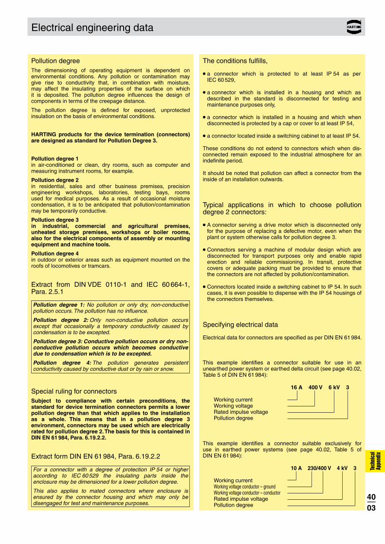
This example identifies a connector suitable for use in an unearthed power system or earthed delta circuit (see page 40.02, Table 5 of DIN EN 61 984):
16 A 400 V 6 kV 3 Working current Working voltage Rated impulse voltage Pollution degree
This example identifies a connector suitable exclusively for use in earthed power systems (see page 40.02, Table 5 of DIN EN 61 984):
10 A 230/400 V 4 kV 3 Working current Working voltage conductor – ground Working voltage conductor – conductor Rated impulse voltage Pollution degree
4004
Tech
nica
l Ap
pend
ix
Electrical engineering data
Other terms explained
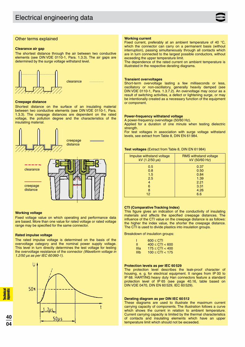
Clearance air gapThe shortest distance through the air between two conductive elements (see DIN VDE 0110-1, Para. 1.3.3). The air gaps are determined by the surge voltage withstand level.
Creepage distanceShortest distance on the surface of an insulating material between two conductive elements (see DIN VDE 0110-1, Para. 1.3.3). The creepage distances are dependent on the rated voltage, the pollution degree and the characteristics of the insulating material.
Working voltageFixed voltage value on which operating and performance data are based. More than one value for rated voltage or rated voltage range may be specified for the same connector.
Rated impulse voltageThe rated impulse voltage is determined on the basis of the overvoltage category and the nominal power supply voltage. This level in turn directly determines the test voltage for testing the overvoltage resistance of the connector (Waveform voltage in 1.2/50 µs as per IEC 60 060-1).
Working current Fixed current, preferably at an ambient temperature of 40 °C, which the connector can carry on a permanent basis (without interruption), passing simultaneously through all contacts which are in turn connected to the largest possible conductors, without exceeding the upper temperature limit. The dependence of the rated current on ambient temperature is illustrated in the respective derating diagrams.
Transient overvoltages Short-term overvoltage lasting a few milliseconds or less, oscillatory or non-oscillatory, generally heavily damped (see DIN VDE 0110-1, Para. 1.3.7.2). An overvoltage may occur as a result of switching activities, a defect or lightening surge, or may be intentionally created as a necessary function of the equipment or component.
Power-frequency withstand voltage A power-frequency overvoltage (50/60 Hz). Applied for a duration of one minute when testing dielectric strength. For test voltages in association with surge voltage withstand levels, see extract from Table 8, DIN EN 61 984.
Test voltages (Extract from Table 8, DIN EN 61 984)
Impulse withstand voltage RMS withstand voltage kV (1.2/50 µs) kV (50/60 Hz)
0.5 0.37 0.8 0.50 1.5 0.84 2.5 1.39 4.0 2.21 6.0 3.31 8.0 4.26 12.0 6.60
CTI (Comparative Tracking Index) This figure gives an indication of the conductivity of insulating materials and affects the specified creepage distances. The influence of the CTI value on the creepage distance is as follows: the higher the index value, the shorter the creepage distance. The CTI is used to divide plastics into insulation groups.
Breakdown of insulation groups:
I 600 ≤ CTI II 400 ≤ CTI < 600 IIIa 175 ≤ CTI < 400 IIIb 100 ≤ CTI < 175
Protection levels as per IEC 60 529 The protection level describes the leak-proof character of housing, e. g. for electrical equipment. It ranges from IP 00 to IP 68. HARTING heavy duty Han connectors feature a standard protection level of IP 65 (see page 40.16, table based on DIN VDE 0470, DIN EN 60 529, IEC 60 529).
Derating diagram as per DIN IEC 60 512 These diagrams are used to illustrate the maximum current carrying capacity of components. The illustration follows a curve which shows the current in relation to ambient temperature. Current carrying capacity is limited by the thermal characteristics of contacts and insulating elements which have an upper temperature limit which should not be exceeded.
clearance
creepage distance
clearance
creepage distance

4005
Tech
nica
l Ap
pend
ix
Current carrying capacity
Current carrying capacity
The current carrying capacity is determined in tests which are conducted on the basis of the DIN IEC 60 512 part 5. The current carrying capacity is limited by the thermal properties of materials which are used for inserts as well as by the insulating materials. These components have a limiting temperature which should not be exceeded.
The relationship between the current, the temperature rise (loss at the contact resistance) and the ambient temperature of the connector is represented by a curve. On a linear co-ordinate system the current lies on the vertical line (ordinate) and the ambient temperature on the horizontal line (abscissa) which ends at the upper limiting temperature.
In another measurement the self-heating (∆t) at different currents is determined.
At least 3 points are determined which are connected to a parabolic curve, the basic curve.
The corrected current carrying capacity curve is derived from this basic curve. The reasons for the correction are external factors that bring an additional limitation to the current carrying capacity, i.e. connectable wire gauge or an unequal dispersion of current.
Example of a current capacity curve
Definition: The rated current is the continuous, not interrupted current a connector can take when simultaneous power on all contacts is given, without exceeding the maximum temperature.
Example of a current carrying curve
Acc. to IEC 61 984 the sum of ambient temperature and the temperature rise of a connector shall not exceed the upper limiting temperature. The limiting temperature is valid for a complete connector, that means insert plus housing.
As a result the insert gives the limit for the temperature of a complete connector and thus housings as well.
In practice it is not usual to load all terminals simultaneously with the maximum current. In such a case one contact can be loaded with a higher current as permitted by the current capacity curve, if less than 20 % of the whole is loaded.
However, for these cases there are no universal rules. The limits have to be determined individually from case to case. It is recommended to proceed in accordance with the relevant rules of the DIN IEC 60 512 part 5.
Current carrying capacity of copper wires
Ambient temperature
Permissible upper temperature-limit set by applied materials
Permissible upper limiting temperature set by applied materials
basic curve
corrected curve
permissible operation range
Upper current limit set by external factors, i.e. connectable wire gauge, given current limit
Cur
rent
car
ryin
g ca
paci
ty
Diameter [mm²] of single wires in a three-phase system 0.75 1,0 1.5 2.5 4 6 10 16 25 35 Type of installation
B1 Wires in protective tubes and installation conduits 7.60 10.4 13.5 18.3 25 32 44 60 77 97
B2 Cables and wires in protective tubes and installation conduits – 9.6 12,0 16.5 23 29 40 53 67 83
C Cables and wires at walls – 11.7 15.2 21,0 28 36 50 66 84 104
D Cables and wires on a bed – 11.5 16.1 22,0 30 37 52 70 88 114
Depiction in accordance with DIN EN 60 204 for PVC-insulated copper wires in an ambient temperature of + 40 °C under permanent operating conditions.For different conditions and temperatures, installations, insulation materials or conductors the relevant corrections have to be carried out.
4006
Tech
nica
l Ap
pend
ix
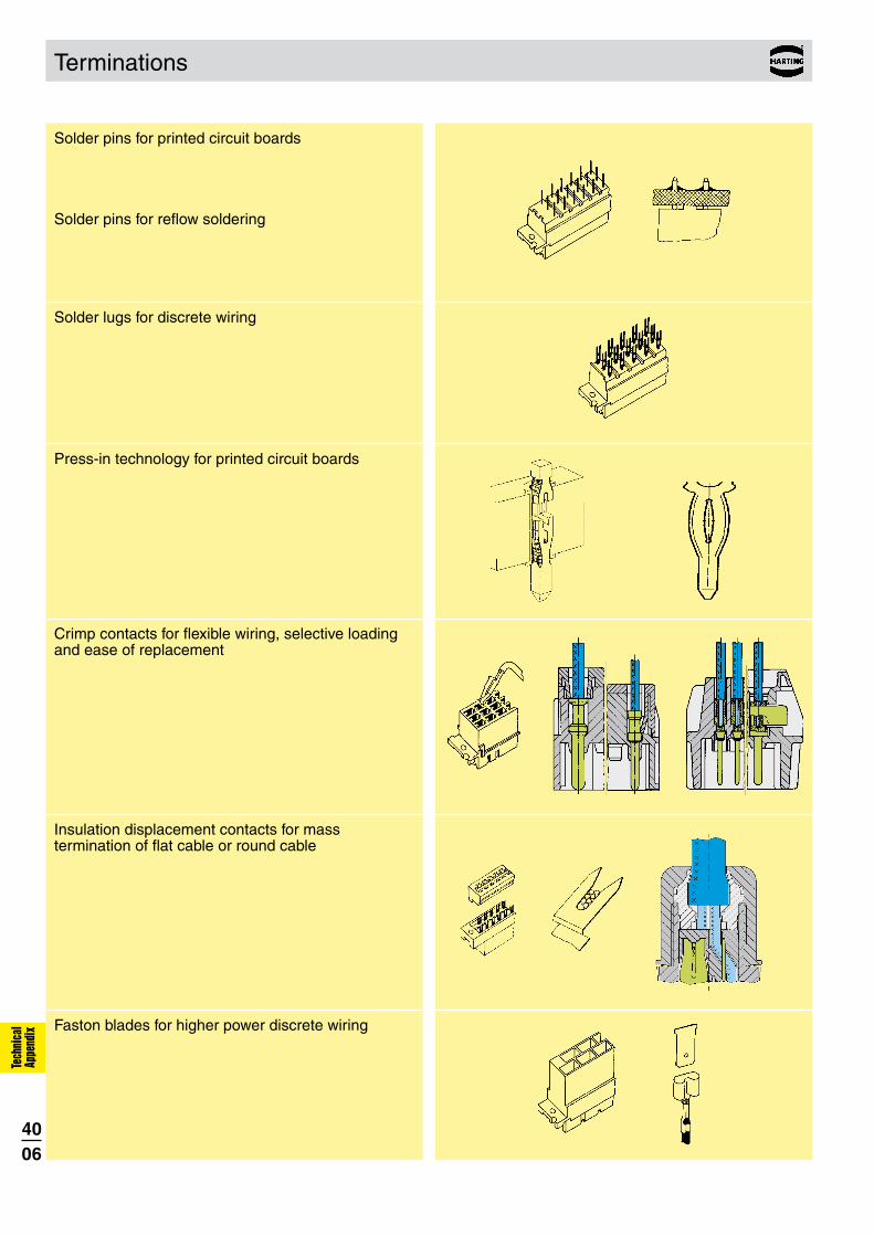
Terminations
Press-in technology for printed circuit boards
Crimp contacts for flexible wiring, selective loading and ease of replacement
Insulation displacement contacts for mass termination of flat cable or round cable
Faston blades for higher power discrete wiring
Solder pins for printed circuit boards
Solder pins for reflow soldering
Solder lugs for discrete wiring

4007
➀ ➁ ➂ ➃
Tech
nica
l Ap
pend
ix
Remarks on the axial screw technique
The wire gauges mentioned in the catalogue refer to geometric wire gauges of cables.
Background: According to DIN VDE 0295 for cables and insulated wires the wire gauge will be determined by conductance (Ω/km) and maximum wire diameter. A minimum cable diameter is not specified! (Example: nominal wire gauge 95 mm² real, geometric wire gauge 89 mm²)
Recommendation: The use of cables with extreme geometric wire gauge deviation should be checked separately with the use of the axial screw ter-mination.
Wire gauge (mm²) 1.5 2.5 4 6 10 16
Screw thread M 3 M 3 M 3.5 M 4 M 4 M 6
Test moment of torque (Nm) 0.5 0.5 0.8 1.2 1.2 1.2*
min. pull-out for 40 50 60 80 90 100stranded wire (N)
with wire protection
* for screws without heads (Han® K 4/8)
One conductor per termination Slot for screwdriver
Screwdriver width: 3.0 x 0.5 mm
Terminations
Screw dimensions and tightening torque for screw terminalsScrew terminal
Screw terminals meet VDE 0609 / EN 60 999. Dimensions and tightening torques for testing are shown opposite.
The relevant regulations state that in the case of
Terminals with wire protection. – the use of ferrules is not necessary
Cage-clamp terminal
This termination method requires very little preparation of the wire and no special tools, leading to a low installed cost and a high degree of mechanical security.
For all stranded and solid wires with a cross section 0.14 to 2.5 mm².
Ease of termination. Conductor and screwdriver are in same plane.
No special preparation of stripped conductor.
The larger the conductor the higher the clamping force.
The termination is vibration-proof.
Guaranteed constant low resistance connection of the cage-clamp terminal.
The cage-clamp system is internationally approved. VDE, SEV, CSA, UL, ÖVE, SEMKO, LCIE (France), Germanischer Lloyd, DET Norske Veritas
Axial screw terminal
This termination associates the benefits of screw and crimp terminals.
Less space required
Easy handling
No special tools
The axial screw termination is suitable for fine strands wires.
Solder connection
The term “soldering” is defined in DIN 8505:
“Soldering is a method of connecting metallic materials using an additional melting metal, if necessary with the assistance of a flux and/or protective gas. The melting temperature of the solder must lie beneath the minimum melting temperature of the base metals being connected. These base metals shall be tinned without melting them-selves.”
Soft solders commonly used on electronic equipment are to DIN 1707-100. Todays lead free solders have a melting range between 217 °C and 227 °C depending on the composition of the alloy. For soldering metallic materials the flux is defined in DIN EN 29 454-1. Tests are explained in DIN 8526.

4008
Tech
nica
l Ap
pend
ix
Press-in technology
Solderless termination for connectors has proven to be reliable for decades. Today the use of press-in connectors encompasses all fields of electrical and electronical applications.
Pressing of electrical components, mainly connectors, is characterised through the matching of the connector pin and the plated through hole of the pcb. Whereas the desired electrical characteristics can be attained relatively independant from the design of the press-in zone, the mechanical characteristics of the press-in zone are crucial for the reliable assembly of connectors where pcb's have different surfaces.
Although the scope of requirements at the press-in process is generally defined in time-tested specifications, the novel press-in zones should offer an optimal handling and a reliable termination. Essentially, this is guaranteed through the design of the press-in zone and the meticulous observance of tolerances. HARTING has been using FEM simulations for the calculation and optimisation of press-in zones for a long period of time. This expertise allows us to simulate various pcb configurations very accurate.
Due to the high deformation resistance and resilience of contacts, they can be easily and repeatedly removed in case of repairs without impairment to their functioning.
is extremely versatile and offers a reliable electrical contact, therefore it is especially well suited for applications with these surfaces.
Please contact us for detailed test reports.
Benefits of the press-in technology
Thermal shocks associated with the soldering process and the risk of the board malfunction are avoided.
No need for the subsequent cleaning of the assembled pcb’s
Additional wrap connections are made possible by using connectors with long pins
Unlimited and efficient processing of partially gold-plated pins for rear I/O - manual soldering is no longer necessary!
bus board with press-in connectors
FEM simulation of the needle eye press-in zone
Board with press-in connectors

4009
Phase 1
Phase 2
Phase 3Te
chni
cal
Appe
ndix
Press-in technology
The processing of press-in connectors can be divided into 3 phases, containing both mechanical and metallurgical operations:
1. Centering and placing of the termination pins
The centering of connectors before pressing is important in order to prevent damage to the pcb and the termination pins. Centering can be omitted when connectors are pressed using a flat rock die.
HARTING offers insert blocks for male connectors to make the centering of connectors unnecessary.
2. Pressing in the pins
In the press-in process the insertion force is continuously transformed into compression force. The resulting friction frees the contacting bars of insulating films. Superfluous plating (tin) is transferred within the plated through hole. A gas-tight connection of fresh non-oxidised metal surfaces is obtained.
3. Obtaining the final position
The press-in operation should be terminated as soon as the connector obtains its final position on the pcb to avoid unnecessary compressive stress. The press-in machines of HARTING feature automatic termination of the press-in operation independant of pcb thickness and surface properties.
The entire dynamic press-in process is characterised through changes of the press-in force that can be statistically evaluated. HARTING records the changes of force with the help of special software. This is an important step towards permanent process control and documented manufacturing data.
The -zone is based on the industry renowned needle eye technology. Its special design allows for compensation of tolerances of pcb surface properties (eg. superfluous tin plating). The excessive material is displaced within the plated through hole, whereby a gas-tight and corrosion resistant electrical connection is assured.
Press die (Flat rock)
Connector
Multilayer pcb
Insert block

4010
Tech
nica
l Ap
pend
ix
Recommended configuration of plated through holes
Sketch: press-in zone in plated through hole
pcb holes for press-in process in acc. to EN 60 352-5
Sn (HAL)
chem. Sn
Au
Ag
pure Cu
Pd
Recommended configuration of plated through holes
In addition to the hot-air-level (HAL) other pcb surfaces are getting more important. Due to their different properties, such as mechanical strength and coefficient of friction we recommend the following configuration of pcb through holes.
Tin-lead plated Hole-Ø 1.15±0.025 mm PCB Cu min. 25 µm (HAL) Sn max. 15 µm acc. EN 60 352-5 Plated hole-Ø 0.94-1.09 mm
Chemical Hole-Ø 1.15±0.025 mm tin-plated PCB Cu min. 25 µm Sn min. 0.8 µm Plated hole-Ø 1.00-1.10 mm
Au / Ni plated PCB Hole-Ø 1.15±0.025 mm Cu min. 25 µm Ni 3-7 µm Au 0.05-0.12 µm Plated hole-Ø 1.00-1.10 mm
Silver plated PCB Hole-Ø 1.15±0.025 mm Cu min. 25 µm Ag 0.1-0.3 µm Plated hole-Ø 1.00-1.10 mm
OSP Hole-Ø 1.15±0.025 mm copper plated PCB Cu min. 25 µm Plated hole-Ø 1.00-1.10 mm
PCB board thickness: ≥ 1.6 mm
Hole-Ø
Cu
e. g. Sn
Plated hole-Ø

4011
Tech
nica
l Ap
pend
ix
Competence in press-in technology
Quality control of the press-in termination
The press-in force correlates with the diameter of the plated through hole and with the friction coefficient of the surface; therefore it can be used for a continuous monitoring of the process.
The retention force, as an indirect measure of the normal force, serves to qualify the process or random tests
HARTING assists you with the most advanced quality assurance methods beyond the usual scope.
The automatic press-in machines of HARTING feature a graphical user interface for monitoring the process and the quality of the press-in termination (see chapter 20).
Typical press-in and retention forces for the D-Sub press-in zone
X-ray photo of a pressed-in connector
Pre
ss-in
forc
e / r
eten
tion
forc
e pe
r pi
n [N
]
Hole diameter [mm]
min./max. retention force
min./max. press-in force

4012
Tech
nica
l Ap
pend
ix
Introduction of the Pin in Hole Intrusive Reflow Process
The continuing trend towards miniaturisation has revolutionised the assembly of electronic components. For the past 15 years, most components have been secured directly to the pcb surface by means of Surface Mount Technology (SMT). By dispensing with drilled holes on the pcb, a space saving of up to 70 percent is achieved.
Today, typical components such as resistors, ICs, capacitors, and connectors with straight terminal pins are almost exclusively fitted using SMD (Surface Mount Device) technology in mass production. In contrast, angled SMD connectors at the edge of the board have not been successful because of tolerance problems (co-planarity) and stresses during mating. Modified solder connectors for assembly with „Pin in Hole Intrusive Reflow“ process offer a better solution. These can be mounted at low cost, utilising existing SMD production lines.
“Pin in Hole Intrusive Reflow“
In this process, the connector is inserted into plated through holes in a comparable way to conventional component mounting. All other components can be assembled on the pcb surface.
The components are positioned using pick-and-place machines. These automatic assembly machines differ according to whether the components are small, lightweight or bulky. Connectors are considered bulky (odd form) because of their comparatively heavy
SMT board with connector for „Pin in Hole Intrusive Reflow“ assembly
weight and large volume which makes them more difficult to grip. Furthermore, machines for odd form components must have higher insertion power to fit the components into pcb holes, which are filled with solder paste. As a rule, modern SMC production lines are equipped with both types of machine, therefore the „Pin in Hole Intrusive Reflow“ process generally entails no extra investment costs for the user.
Conventional assembly process:
1. Application of solder paste
2. Positioning the components
3. Positioning odd form components
4. Reflow soldering
5. Pressing in or partially dip soldering the connector at the board edge
6. Quality inspection
„Pin in Hole Intrusive Reflow“ assembly:
1. Application of solder paste
2. Positioning the components
3. Positioning odd form components
4. Reflow soldering
5. Pressing in or partially dip soldering the connector at the board edge
6. Quality inspection
Pick-and-place machine for odd form components (Courtesy of JOT Automation GmbH)

4013
Tech
nica
l Ap
pend
ix
Solder requirements
Application of solder paste
Before the components are assembled, solder paste must be applied to all the solder pads (for connecting surface-mount components) and the plated through contacts (pcb holes for „Pin in Hole Intrusive Reflow“ insertion). Usually a screen printing process is used for this purpose. A squeegee moves across the pcb, which is masked with screens and presses the solder paste into all unmasked areas. To ensure that the plated through holes are completely filled, significantly more solder paste must be applied than traditional solder pads on the pcb surface. The required quantity can be set exactly via several parameters.
As an alternative to screen printing, the solder paste can be applied by means of a dispenser. A high- precision robot moves the dispenser to all required positions on the pcb. The dispensing method is particularly suitable for small pcb’s or applications which demand high precision and flexibility in dispensing volumes.
Volume of solder paste Connector termination
Dispenser in operation Plated through hole with connector termination
Requirements for the solder connection
There are numerous scientific studies dealing with calculation of the required quantity of solder paste. These studies use various parameters, e.g. the shrinking factor of the paste during soldering or the thickness of the screens used for masking the pcb. Since such calculation methods are complicated to apply, the following rule of thumb has proved valuable in practice:
VPaste = 2(VH – VP)
in which:
VPaste = Required volume of solder paste
VH = Volume of the plated through hole
VP = Volume of the connector termination in the hole
Comment: the multiplier „2“ compensates for solder paste shrinkage during soldering. For this purpose, it was assumed that 50 % of the paste consists of the actual solder, the other 50 % being soldering aids.
At the beginning of a new production batch, the process parameters, such as quantity of solder paste and soldering temperature, can be set by interpreting simple cross-sections of the soldered connection. A reliable measure for achieving optimum parameters is the quantity of solder required to fill the hole. In soldered connections of high quality, the holes are filled to between 75 % and 100 %.
pcb

4014
Tech
nica
l Ap
pend
ix
Requirements for SMC connectors
SMC connectors
SMC (Surface Mount Compatible) connectors have to withstand temperatures of up to 225°C in the reflow oven for 10 to 15 seconds. Therefore, the moulding must be made from a dimensionally stable plastic which expands at the same rate as the pcb material when subjected to heat.
The length of the connector contacts should be such that they protrude by no more than 1.5 millimetres after insertion to the pcb. Each contact collects solder on its tip as it penetrates the solder paste in the hole. So if the contact was too long, this solder would no longer be able to reflow back into the plated through hole by capillary action during the soldering process, therefore the quality of the soldered connection would suffer as a result.
Connector design must permit both automatic assembly with pick-and-place machines and manual positioning for test and pre-production batches. It is also important for the packaging of the connectors to be suitable for automated assembly. Experience shows that deep-drawn film and reel packaging fed into the pick-and-place machines with the aid of a conveyor system is particularly suitable.
Advantages for using SMC connectors are: Partial dip soldering or press-in
is no longer required High mechanical stability Complete compatibility
with Surface Mount Technology Savings through integration
into the automated assembly process Reduced floor space in the production plant
HARTING connector mounted in a tape ready for automatic placement.
HARTING SMC technology
HARTING offers its customers a complete system concept for integrating SMC technology into existing production lines. We manufacture a wide range of SMC connectors (3 and 5 row) in compliance with IEC 60 603-2, D-Sub connectors in compliance with IEC 60 807 and connectors from the har-mik® series with contact spacing of 1.27 millimetres. In addition, HARTING supports the market with packaging and processing concepts, which have been developed in collaboration with renowned manufacturers of SMC soldering and assembly plants.
Advantages of the „Pin in Hole Intrusive Reflow“ process:
• Partial dip soldering or press fitting is no longer required
• Complete compatibility with Surface Mount Technology
• Complete integration into the automated assembly process
• Reduced floor space in the production plant
• As a rule, no additional investment costs
HARTING connector mounted in a tape ready for placement using an odd form assembly station.
4015
mm² AWG N
Tech
nica
l Ap
pend
ix
Terminations
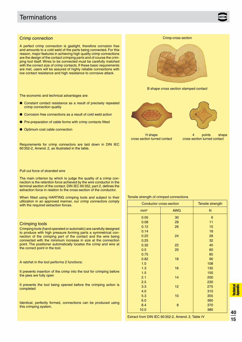
Crimp connection
A perfect crimp connection is gastight, therefore corrosion free and amounts to a cold weld of the parts being connected. For this reason, major features in achieving high quality crimp connections are the design of the contact crimping parts and of course the crim-ping tool itself. Wires to be connected must be carefully matched with the correct size of crimp contacts. If these basic requirements are met, users will be assured of highly reliable connections with low contact resistance and high resistance to corrosive attack.
The economic and technical advantages are:
Constant contact resistance as a result of precisely repeated crimp connection quality
Corrosion free connections as a result of cold weld action
Pre-preparation of cable forms with crimp contacts fitted
Optimum cost cable connection
Requirements for crimp connectors are laid down in DIN IEC 60 352-2, Amend. 2, as illustrated in the table.
Pull out force of stranded wire
The main criterion by which to judge the quality of a crimp con-nection is the retention force achieved by the wire conductor in the terminal section of the contact. DIN IEC 60 352, part 2, defines the extraction force in relation to the cross-section of the conductor.
When fitted using HARTING crimping tools and subject to their utilization in an approved manner, our crimp connectors comply with the required extraction forces.
Crimp-cross section
Crimping toolsCrimping tools (hand operated or automatic) are carefully designed to produce with high pressure forming parts a symmetrical con-nection of the crimping part of the contact and the wire being connected with the minimum increase in size at the connection point. The positioner automatically locates the crimp and wire at the correct point in the tool.
A ratchet in the tool performs 2 functions:
It prevents insertion of the crimp into the tool for crimping before the jaws are fully open
It prevents the tool being opened before the crimping action is completed
Identical, perfectly formed, connections can be produced using this crimping system.
Tensile strength of crimped connections
Conductor cross-section Tensile strength
0.05 30 6 0.08 28 11 0.12 26 15 0.14 18 0.22 24 28 0.25 32 0.32 22 40 0.50 20 60 0.75 85 0.82 18 90 1.00 108 1.30 16 135 1.50 150 2.10 14 200 2.50 230 3.30 12 275 4.00 310 5.30 10 355 6.00 360 8.40 8 370 10.00 380
Extract from DIN IEC 60 352-2, Amend. 2, Table IV
B shape cross section stamped contact
H shape 4 points shape cross section turned contact cross section turned contact

4016
0 0
1 1
2 2
3 3
4 4
5 5
6 6
7
8
Tech
nica
l Ap
pend
ix
Hoods/housings connector insert protection
The connector’s housing, sealing and locking mechanism protect the connection from external influences such as mechanical shocks, foreign bodies, humidity, dust, water or other fluids such as cleansing and cooling agents, oils, etc. The degree of protection the housing offers is explained in the IEC 60 529, DIN EN 60 529, standards that categorize enclosures according to foreign body and water protection.The following table shows the different degrees of protection.
Code letters First Index Figure Second Index Figure (International Protection) (Foreign bodies protection) (Water protection)
IP 6 5
Description according to DIN EN 60 529, IEC 60 529
Index Degree of protection figure Index Degree of protection figure
No protection against accidental contact, no protection against solid foreign bodies
No protection
No protection against water
No protection against water
Protection against contact with any large area by hand and against large solid foreign bodies with Ø > 50 mm
Protection against large foreign bodies
Protection against vertical water drips
Drip-proof
Protection against con-tact with the fingers, protection against solid foreign bodies with Ø > 12 mm
Protection against medium sized foreign bodies
Protection against water drips (up to a 15° angle)
Drip-proof
Protection against tools, wires or similar objects with Ø > 2.5 mm, protection against small foreign solid bodies with Ø > 2.5 mm
Protection against small solid foreign bodies
Protection against diagonal water drips (up to a 60° angle)
Spray-proof
As 3 however Ø > 1 mm
Protection against grain-shaped foreign bodies
Protection against splashed water from all directions
Splash-proof
Full protection against contact. Protection against interior injurious dust deposits
Protection against injurious deposits of dust
Protection against water (out of a nozzle) from all directions
Hose-proof
Total protection against contact. Protection against penetration of dust
Protection against ingress of dust
Protection against strong water (out of a nozzle) from all directions
Strong hose-proof
Protected against temporary immersion
Protected against immersion
Protected against water pressure
Water-tight


