

LCD TVSERVICE MANUAL
CAUTIONBEFORE SERVICING THE CHASSIS,READ THE SAFETY PRECAUTIONS IN THIS MANUAL.
CHASSIS : LA84D
MODEL : 42LG50 42LG50-UG
website:http://biz.LGservice.com
Internal Use Only
- 2 -Copyright © 2008 LG Electronics. Inc. All right reserved. Only for training and service purposes
LGE Internal Use Only
CONTENTS
CONTENTS ............................................................................................. 2
PRODUCT SAFETY ................................................................................. 3
SPECIFICATION ....................................................................................... 6
ADJUSTMENT INSTRUCTION ................................................................ 9
TROUBLE SHOOTING .......................................................................... 14
BLOCK DIAGRAM.................................................................................. 20
EXPLODED VIEW .................................................................................. 24
SVC. SHEET ...............................................................................................
- 3 -Copyright © 2008 LG Electronics. Inc. All right reserved. Only for training and service purposes
LGE Internal Use Only
SAFETY PRECAUTIONS
Many electrical and mechanical parts in this chassis have special safety-related characteristics. These parts are identified by in theSchematic Diagram and Replacement Parts List. It is essential that these special safety parts should be replaced with the same components as recommended in this manual to preventShock, Fire, or other Hazards. Do not modify the original design without permission of manufacturer.
General Guidance
An isolation Transformer should always be used during theservicing of a receiver whose chassis is not isolated from the ACpower line. Use a transformer of adequate power rating as thisprotects the technician from accidents resulting in personal injuryfrom electrical shocks.
It will also protect the receiver and it's components from beingdamaged by accidental shorts of the circuitry that may beinadvertently introduced during the service operation.
If any fuse (or Fusible Resistor) in this TV receiver is blown,replace it with the specified.
When replacing a high wattage resistor (Oxide Metal Film Resistor,over 1W), keep the resistor 10mm away from PCB.
Keep wires away from high voltage or high temperature parts.
Before returning the receiver to the customer,
always perform an AC leakage current check on the exposedmetallic parts of the cabinet, such as antennas, terminals, etc., tobe sure the set is safe to operate without damage of electricalshock.
Leakage Current Cold Check(Antenna Cold Check)With the instrument AC plug removed from AC source, connect anelectrical jumper across the two AC plug prongs. Place the ACswitch in the on position, connect one lead of ohm-meter to the ACplug prongs tied together and touch other ohm-meter lead in turn toeach exposed metallic parts such as antenna terminals, phonejacks, etc. If the exposed metallic part has a return path to the chassis, themeasured resistance should be between 1MΩ and 5.2MΩ. When the exposed metal has no return path to the chassis thereading must be infinite.An other abnormality exists that must be corrected before thereceiver is returned to the customer.
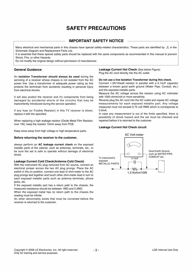
Leakage Current Hot Check (See below Figure) Plug the AC cord directly into the AC outlet.
Do not use a line Isolation Transformer during this check.Connect 1.5K/10watt resistor in parallel with a 0.15uF capacitorbetween a known good earth ground (Water Pipe, Conduit, etc.)and the exposed metallic parts.Measure the AC voltage across the resistor using AC voltmeterwith 1000 ohms/volt or more sensitivity.Reverse plug the AC cord into the AC outlet and repeat AC voltagemeasurements for each exposed metallic part. Any voltagemeasured must not exceed 0.75 volt RMS which is corresponds to0.5mA.In case any measurement is out of the limits specified, there ispossibility of shock hazard and the set must be checked andrepaired before it is returned to the customer.
Leakage Current Hot Check circuit
1.5 Kohm/10W
To Instrument'sexposed METALLIC PARTS
Good Earth Groundsuch as WATER PIPE,CONDUIT etc.
AC Volt-meter
IMPORTANT SAFETY NOTICE
0.15uF
Copyright © 2008 LG Electronics. Inc. All right reserved. Only for training and service purposes
LGE Internal Use Only- 4 -
CAUTION: Before servicing receivers covered by this servicemanual and its supplements and addenda, read and follow theSAFETY PRECAUTIONS on page 3 of this publication.NOTE: If unforeseen circumstances create conflict between thefollowing servicing precautions and any of the safety precautions onpage 3 of this publication, always follow the safety precautions.Remember: Safety First.
General Servicing Precautions1. Always unplug the receiver AC power cord from the AC power
source before;a. Removing or reinstalling any component, circuit board
module or any other receiver assembly.b. Disconnecting or reconnecting any receiver electrical plug or
other electrical connection.c. Connecting a test substitute in parallel with an electrolytic
capacitor in the receiver.CAUTION: A wrong part substitution or incorrect polarityinstallation of electrolytic capacitors may result in anexplosion hazard.
2. Test high voltage only by measuring it with an appropriate highvoltage meter or other voltage measuring device (DVM,FETVOM, etc) equipped with a suitable high voltage probe.Do not test high voltage by "drawing an arc".
3. Do not spray chemicals on or near this receiver or any of itsassemblies.
4. Unless specified otherwise in this service manual, cleanelectrical contacts only by applying the following mixture to thecontacts with a pipe cleaner, cotton-tipped stick or comparablenon-abrasive applicator; 10% (by volume) Acetone and 90% (byvolume) isopropyl alcohol (90%-99% strength)CAUTION: This is a flammable mixture.Unless specified otherwise in this service manual, lubrication ofcontacts in not required.
5. Do not defeat any plug/socket B+ voltage interlocks with whichreceivers covered by this service manual might be equipped.
6. Do not apply AC power to this instrument and/or any of itselectrical assemblies unless all solid-state device heat sinks arecorrectly installed.
7. Always connect the test receiver ground lead to the receiverchassis ground before connecting the test receiver positivelead.Always remove the test receiver ground lead last.
8. Use with this receiver only the test fixtures specified in thisservice manual.CAUTION: Do not connect the test fixture ground strap to anyheat sink in this receiver.
Electrostatically Sensitive (ES) DevicesSome semiconductor (solid-state) devices can be damaged easilyby static electricity. Such components commonly are calledElectrostatically Sensitive (ES) Devices. Examples of typical ESdevices are integrated circuits and some field-effect transistors andsemiconductor "chip" components. The following techniquesshould be used to help reduce the incidence of componentdamage caused by static by static electricity.1. Immediately before handling any semiconductor component or
semiconductor-equipped assembly, drain off any electrostaticcharge on your body by touching a known earth ground.Alternatively, obtain and wear a commercially availabledischarging wrist strap device, which should be removed toprevent potential shock reasons prior to applying power to the
unit under test.2. After removing an electrical assembly equipped with ES
devices, place the assembly on a conductive surface such asaluminum foil, to prevent electrostatic charge buildup orexposure of the assembly.
3. Use only a grounded-tip soldering iron to solder or unsolder ESdevices.
4. Use only an anti-static type solder removal device. Some solderremoval devices not classified as "anti-static" can generateelectrical charges sufficient to damage ES devices.
5. Do not use freon-propelled chemicals. These can generateelectrical charges sufficient to damage ES devices.
6. Do not remove a replacement ES device from its protectivepackage until immediately before you are ready to install it.(Most replacement ES devices are packaged with leadselectrically shorted together by conductive foam, aluminum foilor comparable conductive material).
7. Immediately before removing the protective material from theleads of a replacement ES device, touch the protective materialto the chassis or circuit assembly into which the device will beinstalled.CAUTION: Be sure no power is applied to the chassis or circuit,and observe all other safety precautions.
8. Minimize bodily motions when handling unpackagedreplacement ES devices. (Otherwise harmless motion such asthe brushing together of your clothes fabric or the lifting of yourfoot from a carpeted floor can generate static electricitysufficient to damage an ES device.)
General Soldering Guidelines1. Use a grounded-tip, low-wattage soldering iron and appropriate
tip size and shape that will maintain tip temperature within therange or 500°F to 600°F.
2. Use an appropriate gauge of RMA resin-core solder composedof 60 parts tin/40 parts lead.
3. Keep the soldering iron tip clean and well tinned.4. Thoroughly clean the surfaces to be soldered. Use a mall wire-
bristle (0.5 inch, or 1.25cm) brush with a metal handle.Do not use freon-propelled spray-on cleaners.
5. Use the following unsoldering techniquea. Allow the soldering iron tip to reach normal temperature.
(500°F to 600°F)b. Heat the component lead until the solder melts.c. Quickly draw the melted solder with an anti-static, suction-
type solder removal device or with solder braid.CAUTION: Work quickly to avoid overheating the circuitboard printed foil.
6. Use the following soldering technique.a. Allow the soldering iron tip to reach a normal temperature
(500°F to 600°F)b. First, hold the soldering iron tip and solder the strand against
the component lead until the solder melts.c. Quickly move the soldering iron tip to the junction of the
component lead and the printed circuit foil, and hold it thereonly until the solder flows onto and around both thecomponent lead and the foil.CAUTION: Work quickly to avoid overheating the circuitboard printed foil.
d. Closely inspect the solder area and remove any excess orsplashed solder with a small wire-bristle brush.
SERVICING PRECAUTIONS
- 5 -Copyright © 2008 LG Electronics. Inc. All right reserved. Only for training and service purposes
LGE Internal Use Only
IC Remove/ReplacementSome chassis circuit boards have slotted holes (oblong) throughwhich the IC leads are inserted and then bent flat against thecircuit foil. When holes are the slotted type, the following techniqueshould be used to remove and replace the IC. When working withboards using the familiar round hole, use the standard techniqueas outlined in paragraphs 5 and 6 above.
Removal1. Desolder and straighten each IC lead in one operation by gently
prying up on the lead with the soldering iron tip as the soldermelts.
2. Draw away the melted solder with an anti-static suction-typesolder removal device (or with solder braid) before removing theIC.
Replacement1. Carefully insert the replacement IC in the circuit board.2. Carefully bend each IC lead against the circuit foil pad and
solder it.3. Clean the soldered areas with a small wire-bristle brush.
(It is not necessary to reapply acrylic coating to the areas).
"Small-Signal" Discrete TransistorRemoval/Replacement1. Remove the defective transistor by clipping its leads as close as
possible to the component body.2. Bend into a "U" shape the end of each of three leads remaining
on the circuit board.3. Bend into a "U" shape the replacement transistor leads.4. Connect the replacement transistor leads to the corresponding
leads extending from the circuit board and crimp the "U" withlong nose pliers to insure metal to metal contact then soldereach connection.
Power Output, Transistor DeviceRemoval/Replacement1. Heat and remove all solder from around the transistor leads.2. Remove the heat sink mounting screw (if so equipped).3. Carefully remove the transistor from the heat sink of the circuit
board.4. Insert new transistor in the circuit board.5. Solder each transistor lead, and clip off excess lead.6. Replace heat sink.
Diode Removal/Replacement1. Remove defective diode by clipping its leads as close as
possible to diode body.2. Bend the two remaining leads perpendicular y to the circuit
board.3. Observing diode polarity, wrap each lead of the new diode
around the corresponding lead on the circuit board.4. Securely crimp each connection and solder it.5. Inspect (on the circuit board copper side) the solder joints of
the two "original" leads. If they are not shiny, reheat them and ifnecessary, apply additional solder.
Fuse and Conventional ResistorRemoval/Replacement1. Clip each fuse or resistor lead at top of the circuit board hollow
stake.2. Securely crimp the leads of replacement component around
notch at stake top.3. Solder the connections.
CAUTION: Maintain original spacing between the replacedcomponent and adjacent components and the circuit board toprevent excessive component temperatures.
Circuit Board Foil RepairExcessive heat applied to the copper foil of any printed circuitboard will weaken the adhesive that bonds the foil to the circuitboard causing the foil to separate from or "lift-off" the board. Thefollowing guidelines and procedures should be followed wheneverthis condition is encountered.
At IC ConnectionsTo repair a defective copper pattern at IC connections use thefollowing procedure to install a jumper wire on the copper patternside of the circuit board. (Use this technique only on ICconnections).
1. Carefully remove the damaged copper pattern with a sharpknife. (Remove only as much copper as absolutely necessary).
2. carefully scratch away the solder resist and acrylic coating (ifused) from the end of the remaining copper pattern.
3. Bend a small "U" in one end of a small gauge jumper wire andcarefully crimp it around the IC pin. Solder the IC connection.
4. Route the jumper wire along the path of the out-away copperpattern and let it overlap the previously scraped end of the goodcopper pattern. Solder the overlapped area and clip off anyexcess jumper wire.
At Other ConnectionsUse the following technique to repair the defective copper patternat connections other than IC Pins. This technique involves theinstallation of a jumper wire on the component side of the circuitboard.
1. Remove the defective copper pattern with a sharp knife.Remove at least 1/4 inch of copper, to ensure that a hazardouscondition will not exist if the jumper wire opens.
2. Trace along the copper pattern from both sides of the patternbreak and locate the nearest component that is directlyconnected to the affected copper pattern.
3. Connect insulated 20-gauge jumper wire from the lead of thenearest component on one side of the pattern break to the leadof the nearest component on the other side.Carefully crimp and solder the connections.CAUTION: Be sure the insulated jumper wire is dressed so theit does not touch components or sharp edges.
Copyright © 2008 LG Electronics. Inc. All right reserved. Only for training and service purposes
LGE Internal Use Only- 6 -
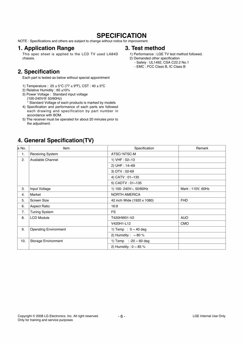
4. General Specification(TV) a No. Item Specification Remark
1. Receiving System ATSC/ NTSC-M
2. Available Channel 1) VHF : 02~13
2) UHF : 14~69
3) DTV : 02-69
4) CATV : 01~135
5) CADTV : 01~135
3. Input Voltage 1) 100- 240V~, 50/60Hz Mark : 110V, 60Hz
4. Market NORTH AMERICA
5. Screen Size 42 inch Wide (1920 x 1080) FHD
6. Aspect Ratio 16:9
7. Tuning System FS
8. LCD Module T420HW01-V2 AUO
V420H1-L12 CMO
9. Operating Environment 1) Temp : 0 ~ 40 deg
2) Humidity : ~ 80 %
10. Storage Environment 1) Temp : -20 ~ 60 deg
2) Humidity : 0 ~ 85 %
1. Application RangeThis spec sheet is applied to the LCD TV used LA84Dchassis.
2. SpecificationEach part is tested as below without special appointment
1) Temperature : 25 ± 5°C (77 ± 9ºF), CST : 40 ± 5ºC2) Relative Humidity : 65 ±10% 3) Power Voltage : Standard input voltage
(100-240V@ 50/60Hz)* Standard Voltage of each products is marked by models
4) Specification and performance of each parts are followedeach drawing and specif ication by part number inaccordance with BOM.
5) The receiver must be operated for about 20 minutes prior tothe adjustment.
3. Test method1) Performance : LGE TV test method followed.2) Demanded other specification
- Safety : UL1492, CSA C22.2 No.1- EMC : FCC Class B, IC Class B
SPECIFICATIONNOTE : Specifications and others are subject to change without notice for improvement.
Copyright © 2008 LG Electronics. Inc. All right reserved. Only for training and service purposes
LGE Internal Use Only- 7 -
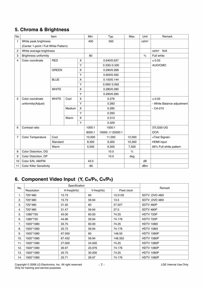
5. Chroma & BrightnessNo. Item Min. Typ. Max. Unit Remark
1 White peak brightness 400 500 cd/m2
(Center 1-point / Full White Pattern)
2 White average brightness cd/m2 N/A
3 Brightness uniformity 80 % Full white
4 Color coordinate RED X 0.640/0.637 ± 0.03
Y 0.330/.0.330 AUO/CMO
GREEN X 0.290/0.268
Y 0.600/0.592
BLUE X 0.150/0.144
Y 0.060/ 0.062
WHITE X 0.280/0.280
Y 0.290/0.285
5 Color coordinate WHITE Cool X 0.276 ± 0.03
uniformity(Adjust) Y 0.283 - White Balance adjustment
Medium X 0.285 - CA-210
Y 0.293
Warm X 0.313
Y 0.329
6 Contrast ratio 1000:1 1500:1 37LG50-UG
8000:1 10000.:1/ 25000:1 DCR
7 Color Temperature Cool 10,000 11,000 12,000 <Test Signal>
Standard 8,300 9,300 10,300 HDMI input
Warm 5,500 6,500 7,500 85% Full white pattern
8 Color Distortion, DG 10.0 %
9 Color Distortion, DP 10.0 deg
10 Color S/N, AM/FM 43.0 dB
11 Color Killer Sensitivity -80 dBm
6. Component Video Input (Y, CB/PB, CR/PR)
No.Specification
RemarkResolution H-freq(kHz) V-freq(Hz) Pixel clock
1. 720*480 15.73 60 13.5135 SDTV ,DVD 480I
2. 720*480 15.73 59.94 13.5 SDTV ,DVD 480I
3. 720*480 31.50 60 27.027 SDTV 480P
4. 720*480 31.47 59.94 27.0 SDTV 480P
5. 1280*720 45.00 60.00 74.25 HDTV 720P
6. 1280*720 44.96 59.94 74.176 HDTV 720P
7. 1920*1080 33.75 60.00 74.25 HDTV 1080I
8. 1920*1080 33.72 59.94 74.176 HDTV 1080I
9. 1920*1080 67.500 60 148.50 HDTV 1080P
10. 1920*1080 67.432 59.94 148.352 HDTV 1080P
11. 1920*1080 27.000 24.000 74.25 HDTV 1080P
12. 1920*1080 26.97 23.976 74.176 HDTV 1080P
13. 1920*1080 33.75 30.000 74.25 HDTV 1080P
14. 1920*1080 33.71 29.97 74.176 HDTV 1080P
Copyright © 2008 LG Electronics. Inc. All right reserved. Only for training and service purposes
LGE Internal Use Only- 8 -
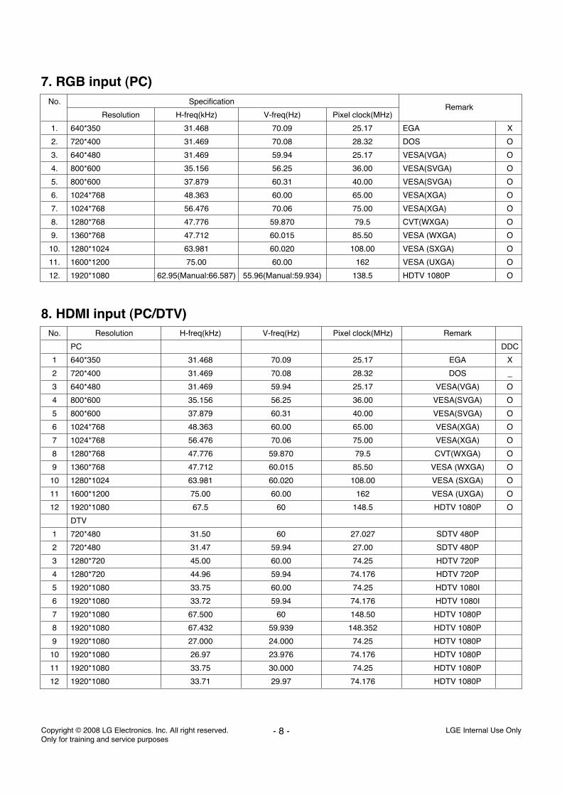
No. Specification Remark
Resolution H-freq(kHz) V-freq(Hz) Pixel clock(MHz)
1. 640*350 31.468 70.09 25.17 EGA X
2. 720*400 31.469 70.08 28.32 DOS O
3. 640*480 31.469 59.94 25.17 VESA(VGA) O
4. 800*600 35.156 56.25 36.00 VESA(SVGA) O
5. 800*600 37.879 60.31 40.00 VESA(SVGA) O
6. 1024*768 48.363 60.00 65.00 VESA(XGA) O
7. 1024*768 56.476 70.06 75.00 VESA(XGA) O
8. 1280*768 47.776 59.870 79.5 CVT(WXGA) O
9. 1360*768 47.712 60.015 85.50 VESA (WXGA) O
10. 1280*1024 63.981 60.020 108.00 VESA (SXGA) O
11. 1600*1200 75.00 60.00 162 VESA (UXGA) O
12. 1920*1080 62.95(Manual:66.587) 55.96(Manual:59.934) 138.5 HDTV 1080P O
7. RGB input (PC)
8. HDMI input (PC/DTV)No. Resolution H-freq(kHz) V-freq(Hz) Pixel clock(MHz) Remark
PC DDC
1 640*350 31.468 70.09 25.17 EGA X
2 720*400 31.469 70.08 28.32 DOS _
3 640*480 31.469 59.94 25.17 VESA(VGA) O
4 800*600 35.156 56.25 36.00 VESA(SVGA) O
5 800*600 37.879 60.31 40.00 VESA(SVGA) O
6 1024*768 48.363 60.00 65.00 VESA(XGA) O
7 1024*768 56.476 70.06 75.00 VESA(XGA) O
8 1280*768 47.776 59.870 79.5 CVT(WXGA) O
9 1360*768 47.712 60.015 85.50 VESA (WXGA) O
10 1280*1024 63.981 60.020 108.00 VESA (SXGA) O
11 1600*1200 75.00 60.00 162 VESA (UXGA) O
12 1920*1080 67.5 60 148.5 HDTV 1080P O
DTV
1 720*480 31.50 60 27.027 SDTV 480P
2 720*480 31.47 59.94 27.00 SDTV 480P
3 1280*720 45.00 60.00 74.25 HDTV 720P
4 1280*720 44.96 59.94 74.176 HDTV 720P
5 1920*1080 33.75 60.00 74.25 HDTV 1080I
6 1920*1080 33.72 59.94 74.176 HDTV 1080I
7 1920*1080 67.500 60 148.50 HDTV 1080P
8 1920*1080 67.432 59.939 148.352 HDTV 1080P
9 1920*1080 27.000 24.000 74.25 HDTV 1080P
10 1920*1080 26.97 23.976 74.176 HDTV 1080P
11 1920*1080 33.75 30.000 74.25 HDTV 1080P
12 1920*1080 33.71 29.97 74.176 HDTV 1080P
1. Application ObjectThese instructions are applied to all of the LCD TV, LA84D.
2. Notes(1) Because this is not a hot chassis, it is not necessary to use
an isolation transformer. However, the use of isolationtransformer will help protect test equipment.
(2) Adjustments must be done in the correct order.(3) The adjustments must be performed in the circumstance of
20±5°C of temperature and 65±10% of relative humidity ifthere is no specific designation.
(4) The input voltage of the receiver be must kept 220V, 60Hzwhen adjusting.
(5) The receiver must be operational for about 15 minutesprior to the adjustments.
(6) Perform preliminary operation after receiving 100% WhitePattern (06CH). (Or 3. White Pattern status of Ez-Adjust)
(7) White Pattern entry method1) Enter into Ez-Adjust by pressing the ADJ key on the
adjustment R/C.2) 100% FULL WHITE PATTERN appears if pressing the
OK (A) key after selecting the 3.WHITE PATTERN withthe CH + / - KEY.
* It is possible to heat run the set without a separate signalgenerator in this mode.
Caution : Care must be taken as afterimage phenomenamay occur about the black level part of screen If leavingpause image turned on for more than 20 minutes(especially inner digital pattern (13 CH), Cross HatchPattern (09CH) with significant black/white contrast).
3. ADC Adjustment3-1. PC input ADC
(1) Auto RGB Gain/Offset Adjustment1) Convert to PC in Input-source
I2C COMMAND:0xF4(SELECT INPUT) 0x00 0x60(RGB)cf. 0x10(TV), 0x20(AV), 0x40(COMPONENT),
0x60(RGB), 0x90(HDMI)2) Signal equipment displays
Output Voltage : 700 mVp-pImpress Resolution XGA (1024x 768 @ 60Hz)
Model : 60 in Pattern GeneratorPattern : 29 in Pattern Generator (MSPG-925 Series)[gray pattern that left & right is black and center iswhite signal (Refer below picture)].
3) Adjust by commanding AUTO_COLOR_ADJUST (0xF1)0x00 0x02 instruction.
(2) Confirmation1) We confirm whether “0xB6(RGB)” address of EEPROM
“0xA2” is “0xAA” or not.2) If “0xB6(RGB)” address of EEPROM “0xB2” isn’t
“0xAA”, we adjust once more.3) We can confirm the ADC values from “0xB0~0xB5
(RGB)” addresses in a page “0xA2”
* Manual ADC process using Service Remote control. Afterenter Service Mode by pushing “ADJ” key, execute “Auto-adjust” by pushing “G” key at “0. ADC CALIBRATION”.
3-2. COMPONENT input ADC(1) Component Gain/Offset Adjustment
1) Convert to Component in Input-sourceI2C command : 0xF4(Select input) 0x00 0x40(Component)cf. 0x10(TV), 0x20(AV), 0x40(COMPONENT),
0x60(RGB), 0x90(HDMI)
2) Signal equipment displaysImpress Resolution 480iMODEL : 209 in Pattern Generator(480i Mode)PATTERN : 08 in Pattern Generator(MSPG-925 Series)
3) Adjust by commanding AUTO_COLOR_ADJUST (0xF1)0x00 0x02 instruction.
4) Signal equipment displayImpress Resolution : 1080i- MODEL: 223 in Pattern Generator(1080i Mode)- PATTERN: 08 in Pattern Generator(MAPG-925 series)
5) Adjust by commanding AUTO_COLOR ADJUST(0xF1)0x00 0x02 instruction.
* Manual ADC process using Service Remote control. Afterenter Service Mode by pushing “ADJ” key, execute “Auto-adjust” by pushing “G” key at “0. ADC CALIBRATION”.
Copyright © 2008 LG Electronics. Inc. All right reserved. Only for training and service purposes
LGE Internal Use Only- 9 -
ADJUSTMENT INSTRUCTION
<Adjustment pattern (PC)>
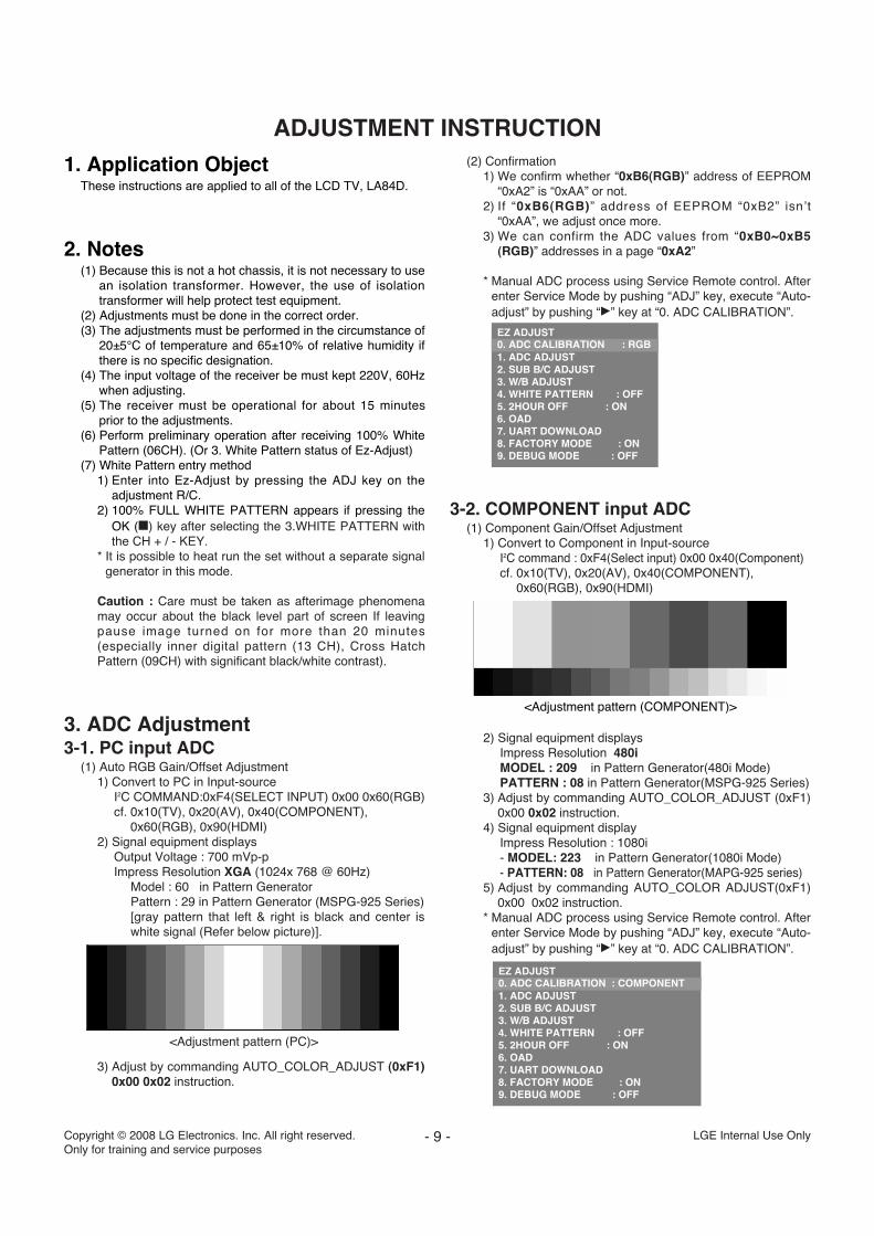
EZ ADJUST
1. ADC ADJUST2. SUB B/C ADJUST3. W/B ADJUST 4. WHITE PATTERN : OFF5. 2HOUR OFF : ON6. OAD7. UART DOWNLOAD8. FACTORY MODE : ON9. DEBUG MODE : OFF
0. ADC CALIBRATION : RGB
<Adjustment pattern (COMPONENT)>
EZ ADJUST
1. ADC ADJUST2. SUB B/C ADJUST3. W/B ADJUST 4. WHITE PATTERN : OFF5. 2HOUR OFF : ON6. OAD7. UART DOWNLOAD8. FACTORY MODE : ON9. DEBUG MODE : OFF
0. ADC CALIBRATION : COMPONENT
(2) Confirmation1) We confirm whether “0xBF(480i)/0xC8(1080i)” address
of EEPROM “0xA2” is “0xAA” or not.2) If “0xBF(480i)/0xC8(1080i)” address of EEPROM “0xA2”
isn’t “0xAA”, we adjust once more.3) We can confirm the ADC values from “0xB ~0xBE(480i)/
0xC2~(1080i)” addresses in a page “0xA2”.
* Manual ADC Confirmation using Service Remocon. Afterenter Service Mode by pushing “INSTART” key.
4. EDID (The Extended Display Identification Data)/ DDC(DisplayData Channel) Download
4-1. Summary It is established in VESA, for communication between PC andMonitor without order from user for building user condition. Ithelps to make easily use realize "Plug and Play" function.
4-2. Required Test Equipment1) PC (with S/W : EDID Data write & Read)2) EDID DOWNLOAD JIG3) HDMI Cable, D-Sub cable
4-3. Connection diagram(Setting of D/L device)
4-4. How to download(1) Configure the download environment as shown at the
adjustment wiring diagram and turn on the PC.(2) Execute the DDC program. (EDID Data Write & Read)(3) Go to Model -> Open, and select the EDID data of the
desired model.(4) Check the item to download from the <Test> item
1) HDMI & RGB: Check Digital & Analog2) (Only)HDMI: Check Digital only
(5) Press ESC(Cancel Mode) -> F8(Auto Mode). (Set AutoDetecting)
(6) Connect the desired signal cable to the set.(7) Make sure that the popup "Proceed to write?" is displayed.(8) Press the Enter key or the space key to download.(9) After downloading, check the OK message and disconnect
the connected cable.
4-5. EDID DATA* It is possible to download on only POWER ON MODE.
- HDMI-1 [C/S : 8A27]EDID Block 0 table =
EDID Block 1 table =
- HDMI-2 [C/S : 8A17]EDID Block 0 table =
EDID Block 1 table =
- 10 -Copyright © 2008 LG Electronics. Inc. All right reserved. Only for training and service purposes
LGE Internal Use Only
MODEL : 22LS4D_UA_UA/LPL_LM220WT7S/W VER : 3.00.1UTT : 6 ADC CAL.
RGB : OKYPbPr(SD) : OKYPbPr(HD) : OK
1. SYNC LEVEL2. DTV SNR3. SCREEN MUTE 4. POWER OFF HISTORY
0. STEREO DETECT
0 1 2 3 4 5 6 7 8 9 A B C D E F
0 00 FF FF FF FF FF FF 00 1E 6D 01 00 01 01 01 01
10 00 11 01 03 80 73 41 96 0A CF 74 A3 57 4C B0 23
20 09 48 4C AF CF 00 31 40 45 40 61 40 81 80 A9 40
30 01 01 01 01 01 01 66 21 50 B0 51 00 1B 30 40 70
40 36 00 C4 8E 21 00 00 1E 02 3A 80 18 71 38 2D 40
50 58 2C 45 00 C4 8E 21 00 00 1E 00 00 00 FD 00 30
60 58 1F 64 11 00 0A 20 20 20 20 20 20 00 00 00 FC
70 00 4C 47 20 54 56 0A 20 20 20 20 20 20 20 01 8A
0 1 2 3 4 5 6 7 8 9 A B C D E F
0 02 03 18 F1 47 84 05 03 02 20 22 10 23 15 07 50
10 67 03 0C 00 10 00 B8 2D 01 1D 00 72 51 D0 1E 20
20 6E 28 55 00 C4 8E 21 00 00 1E 01 1D 80 18 71 1C
30 16 20 58 2C 25 00 C4 8E 21 00 00 9E 8C 0A D0 8A
40 20 E0 2D 10 10 3E 96 00 C4 8E 21 00 00 18 8C 0A
50 D0 8A 20 E0 2D 10 10 3E 96 00 13 8E 21 00 00 18
60 26 36 80 A0 70 38 1F 40 30 20 25 00 C4 8E 21 00
70 00 1A 00 00 00 00 00 00 00 00 00 00 00 00 00 27
0 1 2 3 4 5 6 7 8 9 A B C D E F
0 00 FF FF FF FF FF FF 00 1E 6D 01 00 01 01 01 01
10 00 11 01 03 80 73 41 96 0A CF 74 A3 57 4C B0 23
20 09 48 4C AF CF 00 31 40 45 40 61 40 81 80 A9 40
30 01 01 01 01 01 01 66 21 50 B0 51 00 1B 30 40 70
40 36 00 C4 8E 21 00 00 1E 02 3A 80 18 71 38 2D 40
50 58 2C 45 00 C4 8E 21 00 00 1E 00 00 00 FD 00 30
60 58 1F 64 11 00 0A 20 20 20 20 20 20 00 00 00 FC
70 00 4C 47 20 54 56 0A 20 20 20 20 20 20 20 01 8A
0 1 2 3 4 5 6 7 8 9 A B C D E F
0 02 03 18 F1 47 84 05 03 02 20 22 10 23 15 07 50
10 67 03 0C 00 20 00 B8 2D 01 1D 00 72 51 D0 1E 20
20 6E 28 55 00 C4 8E 21 00 00 1E 01 1D 80 18 71 1C
30 16 20 58 2C 25 00 C4 8E 21 00 00 9E 8C 0A D0 8A
40 20 E0 2D 10 10 3E 96 00 C4 8E 21 00 00 18 8C 0A
50 D0 8A 20 E0 2D 10 10 3E 96 00 13 8E 21 00 00 18
60 26 36 80 A0 70 38 1F 40 30 20 25 00 C4 8E 21 00
70 00 1A 00 00 00 00 00 00 00 00 00 00 00 00 00 17
Copyright © 2008 LG Electronics. Inc. All right reserved. Only for training and service purposes
LGE Internal Use Only- 11 -
- HDMI-3 [C/S : 8A07]EDID Block 0 table =
EDID Block 1 table =
- RGB [C/S : F6BC]EDID Block 0 table =
EDID Block 1 table =
5. White Balance5-1. Summary
(1) Purpose: to reduce the difference in color temperatureamong modules
(2) Principal: A module is in full dynamic range when RGBGain on OSD is 192. To adjust the white balance withoutcausing full dynamic range and full data, fix one of RGBGains at 192 and control the other two by reducing themfrom 192.
5-2. Required Equipment(1) Color Analyzer : CA-210 (NCG : CH 9 / WCG : CH12)(2) Automatic adjuster (with automatic adjustment necessity
and the RS-232C communication being possible)(3) Remote control for adjustment(4) Video Signal Generator MSPG-925F 720p, 216Gray
(Model : 217, Pattern 78) => Applied only when the innerpattern cannot be used
* Use the Color Analyzer with the matrix calibrated by the CS-1000
5-3. Adjustment command (Protocol)(1) Protocol
<Command Format>
- LEN : Number of Data Byte- CMD : Command- VAL : Value of FOS Data- CS : Checksum- A : AcknowledgeEx) [Send: JA_00_DD] / [Ack: A_00_okDDX
(2) RS-232C Command(Automatic adjustment)
0 1 2 3 4 5 6 7 8 9 A B C D E F
0 00 FF FF FF FF FF FF 00 1E 6D 01 00 01 01 01 01
10 00 11 01 03 80 73 41 96 0A CF 74 A3 57 4C B0 23
20 09 48 4C AF CF 00 31 40 45 40 61 40 81 80 A9 40
30 01 01 01 01 01 01 66 21 50 B0 51 00 1B 30 40 70
40 36 00 C4 8E 21 00 00 1E 02 3A 80 18 71 38 2D 40
50 58 2C 45 00 C4 8E 21 00 00 1E 00 00 00 FD 00 30
60 58 1F 64 11 00 0A 20 20 20 20 20 20 00 00 00 FC
70 00 4C 47 20 54 56 0A 20 20 20 20 20 20 20 01 8A
0 1 2 3 4 5 6 7 8 9 A B C D E F
0 02 03 18 F1 47 84 05 03 02 20 22 10 23 15 07 50
10 67 03 0C 00 30 00 B8 2D 01 1D 00 72 51 D0 1E 20
20 6E 28 55 00 C4 8E 21 00 00 1E 01 1D 80 18 71 1C
30 16 20 58 2C 25 00 C4 8E 21 00 00 9E 8C 0A D0 8A
40 20 E0 2D 10 10 3E 96 00 C4 8E 21 00 00 18 8C 0A
50 D0 8A 20 E0 2D 10 10 3E 96 00 13 8E 21 00 00 18
60 26 36 80 A0 70 38 1F 40 30 20 25 00 C4 8E 21 00
70 00 1A 00 00 00 00 00 00 00 00 00 00 00 00 00 07
0 1 2 3 4 5 6 7 8 9 A B C D E F
0 00 FF FF FF FF FF FF 00 1E 6D 01 00 01 01 01 01
10 00 11 01 03 18 73 41 96 0A CF 74 A3 57 4C B0 23
20 09 48 4C AF CF 00 31 40 45 40 61 40 81 80 A9 40
30 01 01 01 01 01 01 66 21 50 B0 51 00 1B 30 40 70
40 36 00 C4 8E 21 00 00 1A 02 3A 80 18 71 38 2D 40
50 58 2C 45 00 C4 8E 21 00 00 1E 00 00 00 FD 00 30
60 58 1F 64 11 00 0A 20 20 20 20 20 20 00 00 00 FC
70 00 4C 47 20 54 56 0A 20 20 20 20 20 20 20 01 F6
0 1 2 3 4 5 6 7 8 9 A B C D E F
0 02 03 04 00 0E 1F 00 80 51 00 1E 30 40 80 37 00
10 C4 8E 21 00 00 1C F1 27 00 A0 51 00 25 30 50 80
20 37 00 C4 8E 21 00 00 1C 26 36 80 A0 70 38 1F 40
30 30 20 25 00 C4 8E 21 00 00 0A 00 00 00 00 00 00
40 00 00 00 00 00 00 00 00 00 00 00 00 00 00 00 00
50 00 00 00 00 00 00 00 00 00 00 00 00 00 00 00 00
60 00 00 00 00 00 00 00 00 00 00 00 00 00 00 00 00
70 00 00 00 00 00 00 00 00 00 00 00 00 00 00 00 BC
Color Analyzer
Computer
Pat tern Generator
RS-232C
RS-232C
RS-232C
Probe
Signal Source
* Not used when the inner pattern of the TV set is used
Connection Diagram of Automatic Adjustment
RS-232C COMMANDMeaning
[CMD ID DATA]
wb 00 00 White Balance adjustment start.
wb 00 10 Start of adjust gain (Inner white pattern)
wb 00 1f End of gain adjust
wb 00 20 Start of offset adjust(Inner white pattern)
wb 00 2f End of offset adjust
wb 00 ff End of White Balance adjust(Inner pattern disappeared)
LEN CMD VAL CS
Ex) wb 00 00 : Start Auto-adjustment of white balance.wb 00 10 : Start Gain Adjustment (Inner pattern) ja 00 ff : Adjustment datajb 00 c0 : ……wb 00 1f : End of Gain adjustment
* (wb 00 20(start), wb 00 2f(end)) -> In the case of Off-set adjustmentwb 00 ff : End of white balance adjustment
(3) Adjustment Map
5-4. Adjustment of White Balance(Automatic Adjustment)
1) The adjustment condition should be set by the Power Onkey.
2) Perform the zero calibration of the Color Analyzer andplace the probe close to the display center.
3) Connect the communication cable (RS-232C).4) Select the desired model of the adjustment program and
perform the adjustment.5) After the adjustment is ended (check the OK sign), check
the adjustment condition for each mode of the set.(Warm, Medium, Cool)
6) Disconnect the probe and the communication cable to endthe adjustment.
* The adjustment should be started with "wb 00 00" andended with "wb 00 ff", and the offset should be adjustedwhen necessary.
5-5. Manual white Balance1) The adjustment condition should be set by the Power On
key.2) Press the ADJ of the R/C to enter into ‘EZ-ADJUST’.3) Select ‘4.WHITE PATTERN’ with the CH +/- key and press
the Enter key for 30 minutes or longer to perform the heatrun.
4) Perform the zero calibration of the Color Analyzer and fixthe sensor with the 10cm or less distance at the center ofthe LCD module surface when adjusting.
5) Press the ADJ of the R/C to select ‘3.W/B ADJUST’ of theEz-Adjust and press the right arrow key(G) to enter into theadjustment mode. (As soon as you press ‘G’, the screen isentered into the full white inner pattern.)
6) Fix one of the R/G/B gains to 192 and decrease theremaining two gains to adjust not to exceed 192.
7) The adjustment is done at three white balances of Cool,Medium and Warm.
* The inner pattern is basically used, and if it is not possible,the adjustment can be done by selecting the HDMI input.NONE, INNER or HDMI can be selected by the bottomoption at the Ez Adjust Menu 7.White Balance menu and it isset to INNER as default. If the adjustment cannot be done bythe inner pattern, select the HDMI to adjust.
* Adjustment environment and reference1) Environment illuminance
Adjust it to 10 LUX or less at the place where the lightsource such as lamp should be blocked at maximum.
2) Probe location: Maintain the Color Analyzer (CA-210) close to themodule surface by 10cm or less and keep the probe ofthe Color Analyzer perpendicular to the modulesurface (80°~ 100°).
3) Aging time- Keep the power on after the aging start (with no power
off) to perform the heat run for 15 minutes or longer.- Make sure that the back light is turned on by using no
signal and the full white pattern or others.
5-6. Reference (1) Brightness: Full white 216 Gray (2) Standard color coordinate and white balance when using
the CS-1000
(3) Standard color coordinate and white balance when usingthe CA-210 (CH 10)
Copyright © 2008 LG Electronics. Inc. All right reserved. Only for training and service purposes
LGE Internal Use Only- 12 -
ITEM Command Data Range Default
(Hex.) (Decimal)
Cmd 1 Cmd 2 Min Max
Cool R-Gain j g 00 C0 TBD
G-Gain j h 00 C0 TBD
B-Gain j i 00 C0 TBD
R-Cut TBD
G-Cut TBD
B-Cut TBD
Medium R-Gain j a 00 C0 TBD
G-Gain j b 00 C0 TBD
B-Gain j c 00 C0 TBD
R-Cut TBD
G-Cut TBD
B-Cut TBD
Warm R-Gain j d 00 C0 TBD
G-Gain j e 00 C0 TBD
B-Gain j f 00 C0 TBD
R-Cut TBD
G-Cut TBD
Mode Color Coordination Temp ∆UV
x y
COOL 0.276 0.283 11000K 0.0000
MEDIUM 0.285 0.293 9300K 0.0000
WARM 0.313 0.329 6500K 0.0000
Mode Color Coordination Temp ∆UV
x y
COOL 0.276±0.002 0.283±0.002 11000K 0.0000
MEDIUM 0.285±0.002 0.293±0.002 9300K 0.0000
WARM 0.313+0.002 0.329±0.002 6500K 0.0000
Copyright © 2008 LG Electronics. Inc. All right reserved. Only for training and service purposes
LGE Internal Use Only- 13 -
6. HDCP SETTING(High-Bandwidth Digital Contents Protection)
1) Set write size to 64 bytes2) Set delay time to 250ms3) Connect D-sub Signal Cable to D-Sub Jack4) Input HDCP key with HDCP-key- in-program5) HDCP Key value is stored on EEPROM(AT24C512) which
is 80~A1 addresses of 0xA0~0xA2 page6) AC off/ on and on HDCP button of MSPG925 and confirm
whether picture is displayed or not of using MSPG9257) HDCP Key value is different among the sets.
7. Select the option by country7-1. Overview
1) The option selection is applied to the North Americanmodel only, which selects the rating related country.
2) Applied models: LA84D Chassis applied None USAModel(Canada, Mexico)
7-2. How to select 1) Press the In-Start key of the R/C and change at 0. AREA
OPTION menu.2) Select 1.USA, 2.CANADA or 3.MEXICO from the country
select according to the destination. At this time, use the Akey to adjust
8. Set the shipping mode (In-stop)- After completing the final test, in order to set the set to the
shipping condition, press the In-Stop key of the R/C to makesure that the set is turned off.
9. GND and resisting pressure test9-1. How to test
(1) Preparing for the automatic test on the GND & resistingpressure - Make sure that the power cord is completely inserted into
the set. (When it is disconnected or loosened, test afterinserting it)
(2) Perform the automatic test on the GND & resisting pressure1) The set with power cord, the cord and the A/V completely
inserted into the tuner is loaded on the pallet and enteredinto the automatic test process.
2) Connect the D-terminal AV JACK tester3) Turn on the automatic (GWS103-4)4) Perform the GND TEST5) If it is not good, the buzzer is operated to notify the test
result to the operator.6) If it is OK, it is automatically switched to the resisting
pressure test. (Disconnect the cord and the A/V from theAV JACK BOX)
6) Perform the resisting pressure test7) If it is not good, the buzzer is operated to notify the test
result to the operator.8) If it is OK, the GOOD LAMP is turned and the stopper is
moves down, and it moves to the next process.
9-2. Items to manage(1) TEST voltage
- GND:1.5KV/min at 100mA- SIGNAL:3KV/min at 100mA
(2) TEST time:1 second(3) TEST POINT
- GND test = between Power cord GND and Signal cablemetal GND
- Resisting pressure test = between Power cord GND andLive & Neutral
(4) LEAKAGE CURRENT: Set to 0.5mArms
10. USB S/W Download (option)10-1. Overview
The USB download is for the quick service response via theS/W upgrade and for applying the S/W upgrade necessary forthe board adjustment
10-2. How to download1) After turning on the set, make sure that the display screen
is turned on.2) When the USB Memory Stick with the upgrade file applied
is inserted into the USB jack on the main board, thefollowing screen (example) is displayed after severalseconds
3) Check the current version at [Current TV Software VersionInformation], check the S/W version to upgrade at[Software file list in USB Memory], and press the Enterbutton of the TV remote controller.
4) Downloading is proceeded as shown at the below screen,and when it is ended, turning on/off is automatically done.(When the automatic proceeding is not smoothly done,manually perform the power On/Off).
5) When downloading is ended, remove the USB MemoryStick from the USB jack.
6) Press the IN-START button of the remote controller tocheck the upgraded S/W version.
Copyright © 2008 LG Electronics. Inc. All right reserved. Only for training and service purposes
LGE Internal Use Only- 14 -
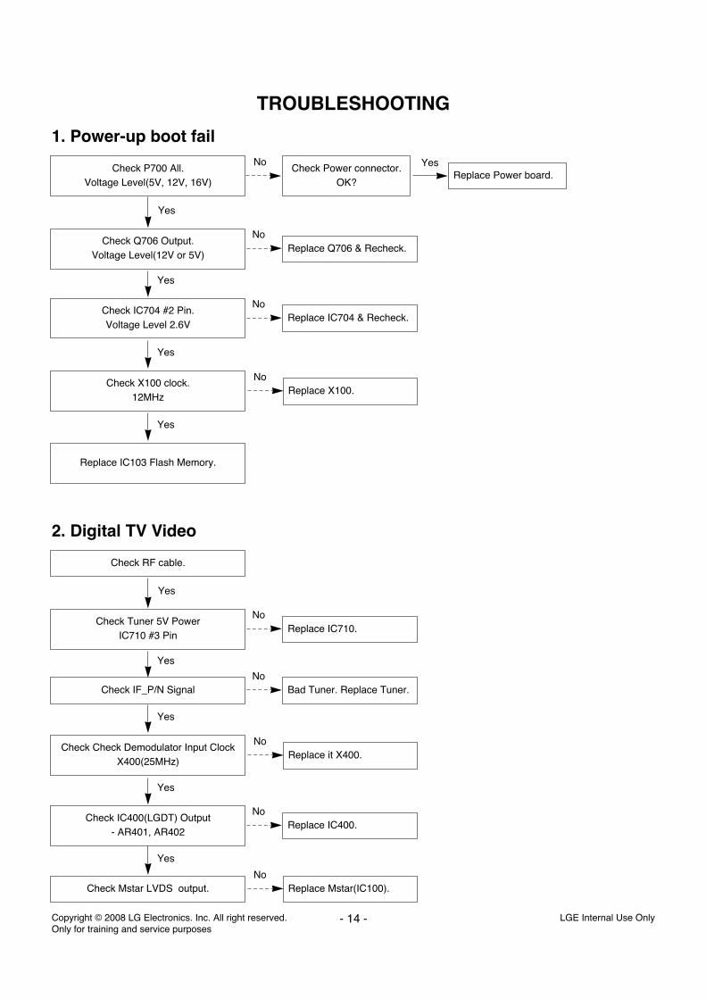
TROUBLESHOOTING
1. Power-up boot fail
Check P700 All.Voltage Level(5V, 12V, 16V)
Check Q706 Output.Voltage Level(12V or 5V)
Check Power connector.OK?
Yes
No
Yes
Check X100 clock.12MHz
Replace Power board.
Replace Q706 & Recheck.
Yes
No
Check IC704 #2 Pin.Voltage Level 2.6V
Yes
Replace IC103 Flash Memory.
Yes
Replace IC704 & Recheck.No
Replace X100.No
2. Digital TV Video
Check RF cable.
Check Tuner 5V PowerIC710 #3 Pin
Yes
Yes
Check Check Demodulator Input ClockX400(25MHz)
Replace IC710.No
Check IF_P/N Signal
Yes
Bad Tuner. Replace Tuner.No
Replace it X400.No
Yes
Check Mstar LVDS output.
Check IC400(LGDT) Output- AR401, AR402
Yes
Replace IC400.No
Replace Mstar(IC100).No
- 15 -Copyright © 2008 LG Electronics. Inc. All right reserved. Only for training and service purposes
LGE Internal Use Only
3. Analog TV Video
4. Component Video
Check RF cable.
Check Tuner 5V Power.IC710 #3 Pin
Yes
Yes
Check CVBS signal.TU402 #16 Pin
Replace IC710.No
Check IIC Line.
Yes
Replace Mstar(IC100).No
Replace Tuner (TU402).No
Yes
Check Mstar LVDS output Replace Mstar(IC100).No
Check Component Cable.
Check JK900/ JK901.
Yes
Yes
Check input signal format.Is it supported?
Yes
Check signal IC903 outputR990, R991, R993
Replace Jack.No
Check signal C1708, C1709, C1710,C1711, C1712, C1713
Yes
Replace it.No
Replace IC903.No
Yes
Check Mstar LVDS output Replace Mstar(IC100).No
- 16 -Copyright © 2008 LG Electronics. Inc. All right reserved. Only for training and service purposes
LGE Internal Use Only
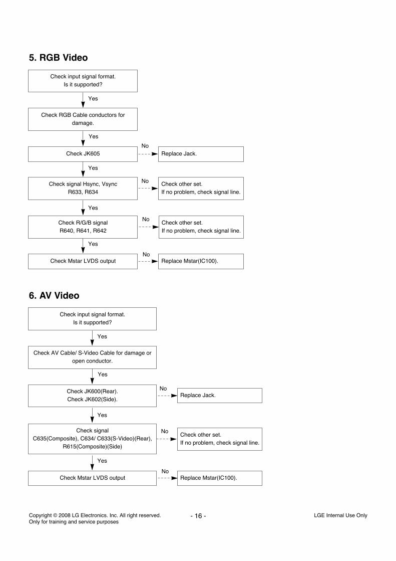
5. RGB Video
Check RGB Cable conductors fordamage.
Check JK605
Yes
Yes
Check input signal format.Is it supported?
Yes
Check R/G/B signalR640, R641, R642
Replace Jack.No
Check signal Hsync, VsyncR633, R634
Yes
Check other set.If no problem, check signal line.
No
Check other set.If no problem, check signal line.
No
Yes
Check Mstar LVDS output Replace Mstar(IC100).No
6. AV Video
Check AV Cable/ S-Video Cable for damage oropen conductor.
Check JK600(Rear).Check JK602(Side).
Yes
Check input signal format.Is it supported?
Yes
Check signalC635(Composite), C634/ C633(S-Video)(Rear),
R615(Composite)(Side)
Replace Jack.No
Yes
Check other set.If no problem, check signal line.
No
Yes
Check Mstar LVDS output Replace Mstar(IC100).No

- 17 -Copyright © 2008 LG Electronics. Inc. All right reserved. Only for training and service purposes
LGE Internal Use Only
Check HDMI Cable conductors fordamage.
Check JK800/ JK801/ JK903
Yes
Yes
Check input signal format.Is it supported?
Yes
Check EDID NVRAM(IC800, 801, 902)Power & I2C Signal (#5, #6)
Replace Jack.No
Check HDMI Signal.
Yes
Check signal line.No
Replace the defective IC or re-downloadEDID data.
No
Check IC802 Voltage Level 3.3V, 5V &Output
Replace Power supply regulator or IC802.No
Check HDCP key NVRAM(IC102)power & I2C Signal (#5, #6)
Replace the defective IC.No
Yes
Yes
Check IC802 clock signal#26, #27
Replace IC802.No
Yes
Replace Mstar (IC100)
Yes
7. HDMI Video
- 18 -Copyright © 2008 LG Electronics. Inc. All right reserved. Only for training and service purposes
LGE Internal Use Only
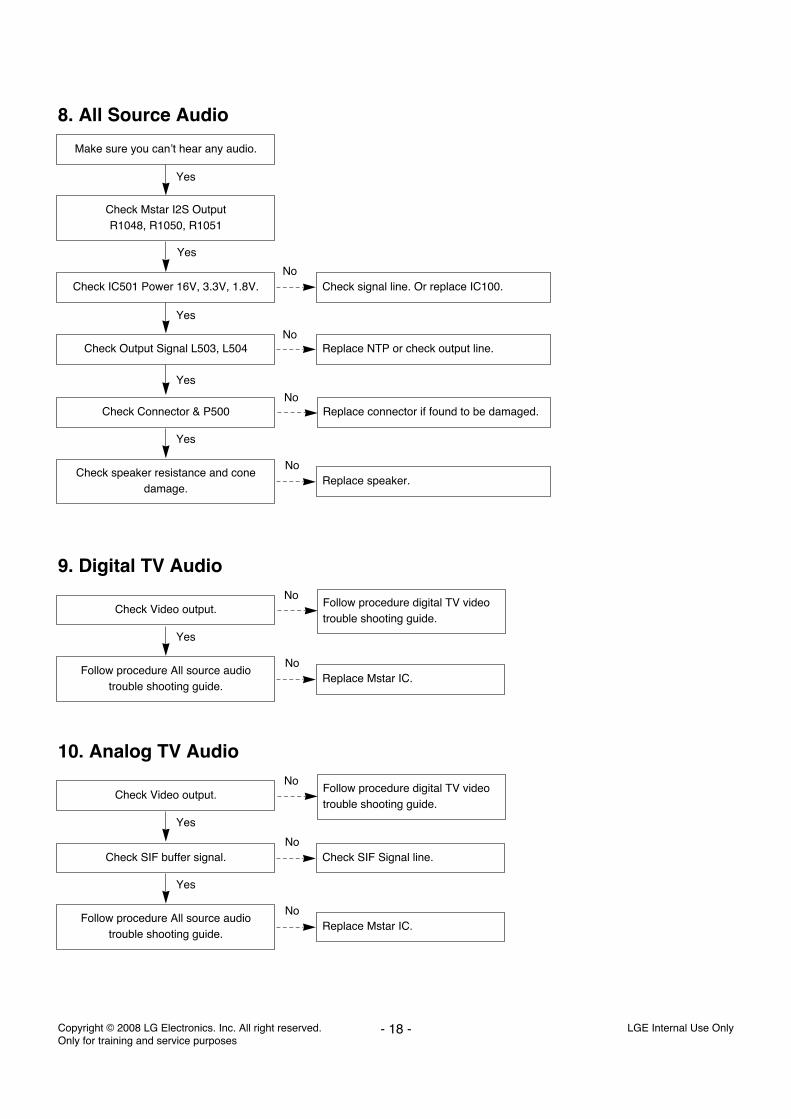
8. All Source Audio
9. Digital TV Audio
Check Mstar I2S OutputR1048, R1050, R1051
Check IC501 Power 16V, 3.3V, 1.8V.
Yes
Yes
Make sure you can’t hear any audio.
Yes
Check Connector & P500
Check signal line. Or replace IC100.No
Check Output Signal L503, L504
Yes
Replace NTP or check output line.No
Replace connector if found to be damaged.No
Yes
Check speaker resistance and conedamage.
Replace speaker.No
Check Video output.Follow procedure digital TV videotrouble shooting guide.
No
Yes
Follow procedure All source audiotrouble shooting guide.
Replace Mstar IC.No
10. Analog TV Audio
Check Video output.Follow procedure digital TV videotrouble shooting guide.
No
Yes
Check SIF buffer signal. Check SIF Signal line.No
Yes
Follow procedure All source audiotrouble shooting guide.
Replace Mstar IC.No

- 19 -Copyright © 2008 LG Electronics. Inc. All right reserved. Only for training and service purposes
LGE Internal Use Only
11. HDMI Audio
Check video output from source device.Follow procedure HDMI videotrouble shooting guide.
No
Yes
Check EDID NVRAM(IC800, IC801, IC802)Power & I2C Signal(#5, #6)
Check SIF Signal line.No
Yes
Follow procedure All source audio troubleshooting guide.
Replace Mstar IC.No

Copyright © 2008 LG Electronics. Inc. All right reserved. Only for training and service purposes
LGE Internal Use Only- 20 -
BLOCK DIAGRAM
1. VIDEO Path
Com
p1(D
VD
/DT
V)
Com
p2(D
VD
/DT
V)
YP
bPr_
2
YP
bPr_
1
AV
1
S-A
V1
AV
2
TU
_CV
BS
AV
_1
AV
_2
MS
TA
R
(Fro
m T
uner
)
RG
B(P
C/D
TV
)R
GB
HD
MI 1
HD
MI 2
H
DM
I 1(T
MD
S)
TMD
SS
witc
h
HD
MI 3
IF_P
/N
S_V
ideo
1_Y
/C
IC80
2
H
DM
I 2(T
MD
S)
H
DM
I 3(T
MD
S)
T
MD
S
IC90
3
Sw
itch
YP
bPr
IC40
0 LG
DT
3304
TP
(MP
EG
Tra
nspo
rt s
trea
m) (F
rom
Tun
er)
IC10
0
- 21 -Copyright © 2008 LG Electronics. Inc. All right reserved. Only for training and service purposes
LGE Internal Use Only
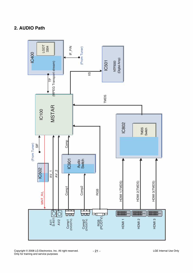
2. AUDIO Path
IC50
2
Com
p1(D
VD
/DT
V)
Com
p2(D
VD
/DT
V)
Com
p1
AV
1
AV
2
S-A
V1
AV
_1
AV
_2
MS
TA
R
RG
B(P
C/D
TV
)R
GB
HD
MI 1
HD
MI 2
Com
p2
SIF
(Fro
m T
uner
)
NTP
3000
(Dig
ital A
mp)
IIS
MN
T_R
/L
H
DM
I 1(T
MD
S)
TMD
SS
witc
h
TMD
SS
witc
h
IC80
2
H
DM
I 2(T
MD
S)
H
DM
I 3(T
MD
S)
T
MD
S
HD
MI 3
Aud
ioS
witc
h
IC90
1C
omp
IF_P
/N
IC40
0 LG
DT
3304
LG
DT
3304
(Fro
m T
uner
)
IC50
1
IC10
0
TP
(MP
EG
Tra
nspo
rt s
trea
m)

- 22 -Copyright © 2008 LG Electronics. Inc. All right reserved. Only for training and service purposes
LGE Internal Use Only
3. Power flow diagram
TU
40
2S
HA
RP
TU
NE
R
Reg
ula
tor
IC
16
V_
AU
DIO
IC7
11
AS
78
09
+5
V_
TU
NE
R1
2V
Q7
06
SI3
86
5B
DV
+5
V_
GE
NE
RA
L+
5V
_S
TIC
70
2A
Z1
11
7H
-3
.3V
+3
.3V
_M
UL
TI
IC7
09
SC
15
65
15
M
+3
.3V
_P
VS
BIC
70
8S
C4
21
5IS
+1
.2V
_P
VS
B
IC8
00
, IC
80
1,
IC9
02
EE
PR
OM
IC8
03
TM
DS
35
1P
AG
IC9
01
CO
MP
AU
DIO
SW
ITC
H
IC6
00
CA
T2
4C
02
WI
IC1
02
AT
24
C5
12
BW
IC5
01
NT
P3
00
0A
IC5
00
AZ
11
17
H-
1.8
V
+1
.8V
_N
TP
12 17
56 19 20
9
4 812
16V
12V
5VS
T
AC
_DE
T
VA
VS
_ON
M5V
_ON
GN
D
5V_M
NT
RL_
ON
18 21
3 7
14 16
13 15
IC4
00
LG
DT
33
04
+3
.3V
_D
VD
D+
3.3
V_
AV
DD
+1
.2V
_D
VD
D
9V
IC7
10
KIA
78
R0
5F
IC8
02
HD
MI
Re
ce
ive
r
- 23 -Copyright © 2008 LG Electronics. Inc. All right reserved. Only for training and service purposes
LGE Internal Use Only
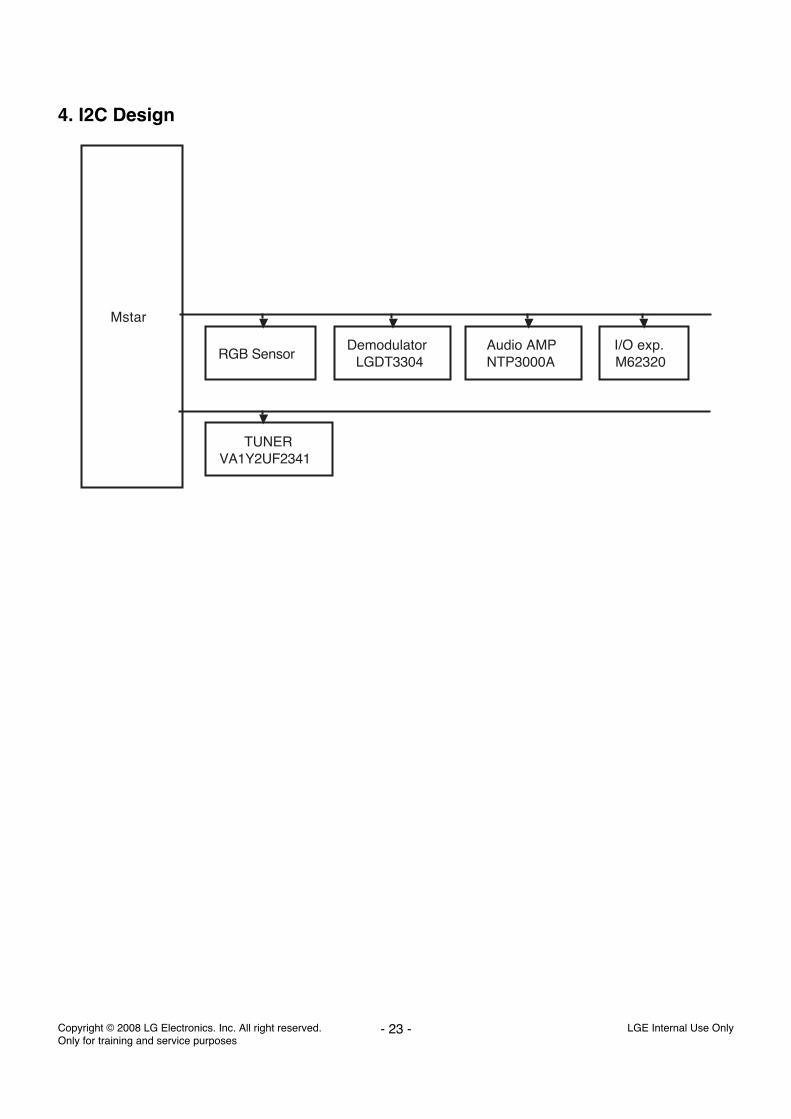
4. I2C Design
Mstar
RGB SensorAudio AMPNTP3000A
DemodulatorLGDT3304
I/O exp.M62320
TUNERVA1Y2UF2341
Copyright © 2008 LG Electronics. Inc. All right reserved. Only for training and service purposes
LGE Internal Use Only- 24 -
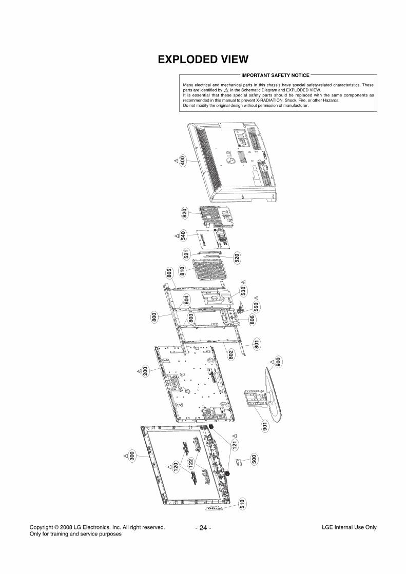
EXPLODED VIEW
300
510
500
120
121
122
200
800
900
901
801
802
803
804
805
806
550
530
810
521
520
540
820
400
Many electrical and mechanical parts in this chassis have special safety-related characteristics. Theseparts are identified by in the Schematic Diagram and EXPLODED VIEW. It is essential that these special safety parts should be replaced with the same components asrecommended in this manual to prevent X-RADIATION, Shock, Fire, or other Hazards. Do not modify the original design without permission of manufacturer.
IMPORTANT SAFETY NOTICE

Copyright LG Electronics. Inc. All right reserved. Only for training and service purposes
C 2008 LGE Internal Use Only
THE SYMBOL MARK OF THIS SCHEMETIC DIAGRAM INCORPORATESSPECIAL FEATURES IMPORTANT FOR PROTECTION FROM X-RADIATION.FILRE AND ELECTRICAL SHOCK HAZARDS, WHEN SERVICING IF IS ESSENTIAL THAT ONLY MANUFATURES SPECFIED PARTS BE USED FORTHE CRITICAL COMPONENTS IN THE SYMBOL MARK OF THE SCHEMETIC.
220K
R133
75
R121
75
R111
SD05
D105
220K
R108
COMP1_R
COMP1_Pb
PC_AUD_RCDS3C05GTA5.6V
D122
COMP1_Y
SD0530VD117
75
R123
5.6V
D103
COMP2_Pr
CDS3C05GTA
5.6V
D123
PPJ209-02
JK100
4A[GN]CONTACT
2A [GN]1P_CAN
3A [GN]O_SPRING
2B [BL]1P_CAN
5B [BL]C_LUG_L
2C [RD]1P_CAN1
5C [RD]C_LUG_L
2D [WH]1P_CAN
5D[WH]C_LUG_L
2E [RD]1P_CAN2
4E[RD]CONTACT
3E [RD]O_SPRING
SD05
D106
5.6V
D104
COMP2_L
220KR119
COMP1_Pr
COMP1_L
75
R12275R110
220KR106
220K
R120
COMP2_Pb
PPJ209-02
JK101
4A
[GN]CONTACT
2A
[GN]1P_CAN
3A
[GN]O_SPRING
2B
[BL]1P_CAN
5B
[BL]C_LUG_L
2C
[RD]1P_CAN1
5C
[RD]C_LUG_L
2D
[WH]1P_CAN
5D
[WH]C_LUG_L
2E
[RD]1P_CAN2
4E
[RD]CONTACT
3E
[RD]O_SPRING
30VD119
SD05
1000-ohm
L100
PC_AUD_L
COMP2_R
220K
R132
SD0530VD118
1000-ohm
L101
SD05
D107
COMP2_Y
75R109
5.6VD115
5.6V
D116
10KR136
10KR143
10KR144
12K
R142
12K
R145
12K
R137
10KR134
12KR135
10KR138
10KR140
12KR139
12K
R141
68R114
DSUB_SCL
75R116
CDS3C30GTH
30VD112
DSUB_SDA
+5V_STCDS3C30GTH
30V
D110
100R125
+5V_MULTI
75R117
DSUB_SDA
DSUB_SCL
0.1uFC100
PC_G
CDS3C30GTH
30V
D114
0.1uFC102
75
R118
4.7K
R112
68R115
0.1uFC101
PC_R
PC_B
PC_VS
68pF
C103
PC_HS
0.1uFC105
4.7KR113
68pF
C104
CDS3C30GTH
30V
D113
100R124
100
R128
4.7KR150
READY
+5V_ST
100
R129
100R130
0.1uF
C110
0.1uFC106
100R131
OPTC111
TXD
0.1uF
C108
0.1uF
C109
OPTC112
RXD
CDS3C30GTH30V
D121
0.1uF
C107
4.7KR151
READY
+3.3V_MST
CDS3C30GTH30V
D120
+5V_ST
EN
KM
C2837-T
112
D1
09A
AC
C
EN
KM
C2837-T
112
D1
11
AA
C
C
EN
KM
C2837-T
112
D1
08A
AC
C
MAX3232CDR
IC101
RS232C
3C1-
2V+
4C2+
1C1+
6V-
5C2-
7DOUT2
8RIN2
9ROUT2
10DIN2
11DIN1
12ROUT1
13RIN1
14DOUT1
15GND
16VCC
PEJ024-01
JK102
6B T_TERMINAL2
8 SHIELD_PLATE
7B B_TERMINAL2
5 T_SPRING
4 R_SPRING
7A B_TERMINAL1
6A T_TERMINAL1
3 E_SPRING
IR_OUT
4.7KR127
4.7KR126
6630TGA004K
KCN-DS-1-0089
JK104
1RED
2GREEN
3BLUE
4GND_1
5DDC_GND
6 RED_GND
7GREEN_GND
8 BLUE_GND
9 NC
10 SYNC_GND
11GND_2
12DDC_DATA
13H_SYNC
14V_SYNC
15DDC_CLOCK
16 SHILED
KCN-DS-1-0088
JK103
1
2
3
4
5
6
7
8
9
10
AT24C02BN-10SU-1.8
IC100
3A2
2A1
4GND
1A0
5SDA
6SCL
7WP
8VCC
1000pFREADY
C113
0R146
1000pFREADY
C114
0R147
1000pFREADY
C115
0R148
1000pFREADY
C116
0R149
COMPONENT2
SDC 15 apply ing check
PC SOUND
COMPONENT1
INPUT1 : COMP1/2,RS232C,PC
PC
RS-232C*ONLY LG30
1.24C02-SUB:0IMMRAL014D
**MULTI ITEM
2.ENKMC2837-SUB:0DS226009AA (KDS226)
SUB : 0IMCRSG010A(STM) MAIN : EAN41348201(TI)
*RS232C TX
THE SYMBOL MARK OF THIS SCHEMETIC DIAGRAM INCORPORATESSPECIAL FEATURES IMPORTANT FOR PROTECTION FROM X-RADIATION.FILRE AND ELECTRICAL SHOCK HAZARDS, WHEN SERVICING IF IS ESSENTIAL THAT ONLY MANUFATURES SPECFIED PARTS BE USED FORTHE CRITICAL COMPONENTS IN THE SYMBOL MARK OF THE SCHEMETIC.
5.6VD216
220KR244
SIDE_RIN
75R241
SD05D214
SIDE_V
220KR242
SIDE_LIN
5.6VD215
75R245
SIDE_Y
75R246
SIDE_C
SD05D217
SD05D218
S_VIDEO_DET
SD05D219
12K
R248
12K
R250
10KR247
10KR249
OPTC210
READY
PPJ218-01
JK204
5C [RD]CONTACT
2C [RD]U_CAN
4C [RD]O_SPRING
2B [WH]U_CAN
3B [WH]C_LUG
2A [YL]U_CAN
5A [YL]CONTACT
4A [YL]O_SPRING
PSJ015-02
JK205
5 O_SPRING
4A C_LUG_L_1
4B C_LUG_S_1
4C C_LUG_L_2
4D C_LUG_S_2
3 GROUND
7SHIELD
0.1uF16V
READY C213
0R252
0R251
100pF50VREADY
C214
100pF50VREADY
C215
75R208
100pF50V
C212
OPT
0R210
470K
R229OPT
RT1C3904-T112
Q203OPT
E
B
C
SD05D201
SPK_R-_HOTEL
5.6V
D208OPT
470K
R230OPT
100pF50V
C211
OPT
PPJ148-10
JK200
4A [RD]O_SPRING
2A [RD]1P_CAN
5A [RD]CONTACT
2 [WH]1P_CAN
3 [WH]C_LUG_L
2B [YL]1P_CAN
4B [YL]O_SPRING
5B [YL]CONTACT
12K
R219
220KR212
0R214
10KR2180R222
100pF50V
C216OPT
5.6V
D209OPT
MNT_ROUT
MNT_LOUT
0R211
OPTC207
CVBS_RIN
12K
R221
1KR236OPT
CVBS_LIN
AUDIO_R
10KR220
10uF
16V
C209
MUTE_LINE
PPJ200-01
JK201
2
1
3
4
5
1KR237OPT
220KR209
SPK_R+_HOTEL
100pF50V
C217OPT
10uF
16V
C208OPT
CVBS_VIN
0R213
5.6VD202
RT1C3904-T112
Q202OPT
E
B
C
5.6VD204
0R223
INPUT2 : CVBS,SIDE AV
SIDE AV
POP NOISE
CVBS
THE SYMBOL MARK OF THIS SCHEMETIC DIAGRAM INCORPORATESSPECIAL FEATURES IMPORTANT FOR PROTECTION FROM X-RADIATION.FILRE AND ELECTRICAL SHOCK HAZARDS, WHEN SERVICING IF IS ESSENTIAL THAT ONLY MANUFATURES SPECFIED PARTS BE USED FORTHE CRITICAL COMPONENTS IN THE SYMBOL MARK OF THE SCHEMETIC.
TMDS3_RX2-
TMDS3_RXC-
HPD_S/W_2
TMDS
2_RX
C-
1KR319
+5V_HDMI_2
HDMI_SEL1
TMDS3_RXC-
HDM
I_C-
HDM
I_SC
LHD
MI_
0-
10KR351
HPD_MST_2
TMDS3_RX0+
TMDS2_RX2-
HDM
I_C+
TMDS1_RX0+
+5V_HDMI_3
4.7K
R362
CEC_C
DDC_SCL1
CEC
TMDS1_RX1-
HDMI1_5V_DET
TMDS
2_RX
1+
HDMI3_5V_DETTMDS2_RXC-
TMDS2_RXC+
0.01
uFC3
10
1KR344
SIDE_HDMI
10KR300
0.01uFC315
HDM
I_0+
+3.3V_MULTI_MST
1KR310
+3.3V
CEC
DDC_
SDA2
0.01
uFC3
14
TMDS3_RX2+
TMDS1_RXC-
HD
MI_
1-
0 .01uFC316
10KR328
HPD_S/W_1
TMDS
2_RX
0+
TMDS2_RX0+
0.01uFC308
TMDS3_RX0-
HD
MI_
2-H
PD_S
/W_3
TMDS3_RX0-
TMDS3_RX1+
HDMI2_5V_DET
10KR324
0 RE
AD
Y
R3
69
TMDS3_RXC+
DDC_SCL3
TMDS1_RXC+
+3.3V_MULTI_MST
+5V_HDMI_2
HPD
_S/W
_2
HPD_MST_1
CEC
BSS83Q306
SBD
G
10KR335
SIDE_HDMI
TMDS1_RX1+
TMDS3_RX1-
TMDS
2_RX
C+
0R3
70
RE
AD
Y
TMDS1_RX2+
4.7KR375
READY
0R373
TMDS2_RX1+
TMDS1_RX0-
+3.3V_HDMI_SW
+5V_ST
4.7K
R361
0R356
TMDS
2_RX
2-
+5V_HDMI_1
TMDS3_RX2-
TMDS3_RX2+
0R358
HDM
I_1+
0 .01uF50V
READY
C307
TMDS2_RX0-
TMDS
2_RX
0-
TMDS1_RX1-
4.7KR374
KDS184S
KD
S184D300A
2
C
A1
10KR329
TMDS2_RX1-
TMDS3_RX0+
0.01
uFC3
11
0.01
uFC3
12
TMDS1_RX2-
+5V_HDMI_3
TMDS3_RX1-
TMDS
2_RX
2+HD
MI_
2+
HDMI_SEL2
TMDS1_RX2+
+5V_HDMI_1
10KR352
TMDS3_RX1+
0.01uFC309
0R357
TMDS1_RXC-
0R355
+5V_ST
TMDS3_RXC+
+5V_HDMI_3
+5V_ST
10KR301
TMDS1_RX2-
+3.3V_HDMI_SW
+5V_HDMI_1
TMDS1_RX0-
TMDS
2_RX
1-
TMDS1_RX1+
HPD_S/W_1
0R368
READY
10KR325
0R347
CEC
HDM
I_SD
ADD
C_SC
L2
+5V_HDMI_2
HPD_S/W_3
TMDS1_RX0+
TMDS2_RX2+
0R345
KDS184S
KD
S184D303A
2
C
A1
DDC_SDA1
0R346
TMDS1_RXC+
CDS3C30GTH
30VD302
READ
Y
HPD_MST_3
DDC_SDA3
KDS184S
KD
S184D301A
2
C
A1
0R350
47KR330
47KR331
47KR326
47KR327
47KR354
47KR353
0READYR365
0READYR376
MM
BD
301L
T1G
30V
D3
04
A C
DDC_SDA2DDC_SCL2
DDC_SDA1DDC_SCL1
DDC_SDA3DDC_SCL3
TMDS351PAGIC302
1SDA3
2SCL3
3GND_1
4B31
5A31
6VCC_1
7B32
8A32
9GND_2
10B33
11A33
12VCC_2
13B34
14A34
15GND_3
16VSADJ
17
Y4
18
Z4
19
VC
C_3
20
Y3
21
Z3
22
GN
D_4
23
Y2
24
Z2
25
VC
C_4
26
Y1
27
Z1
28
GN
D_5
29
SC
L_S
INK
30
SD
A_S
INK
31
HP
D_S
INK
32
S1
33 S234 EQ35 HPD136 SDA137 SCL138 B1139 A1140 VCC_541 B1242 A1243 GND_644 B1345 A1346 VCC_647 B1448 A14
49
VD
D5
0H
PD
25
1S
DA
25
2S
CL
25
3B
21
54
A21
55
VC
C_7
56
B2
25
7A
22
58
GN
D_7
59
B2
36
0A
23
61
VC
C_8
62
B2
46
3A
24
64
HP
D3
0READY
R383
0.01uF50V
C301
0.01uF50V
C313
0.01uF50V
C300
51KR333
30KR334READY
4.7K1%
R372
JP1115
JP1116
JP1117
JP1118
JP1119
JP1120
2SC3875S
RT1C3904-T112
Q300
E
B
C
2SC3875SRT1C3904-T112
Q301
E
B
C
2SC3875SQ307
SIDE_HDMIE
B
C
DC1R019NBHJK303
SIDE_HDMI
14 NC
13 CEC
5 DATA1_SHIELD
20
JACK_GND
12 CLK-
11 CLK_SHIELD
2 DATA2_SHIELD
19 HPD
18+5V_POWER
10 CLK+
4 DATA1+
1 DATA2+
17DDC/CEC_GND
9 DATA0-
8 DATA0_SHIELD
3 DATA2-
16 SDA
7 DATA0+
6 DATA1-
15 SCL
47KR371
+3.3V
200
R332
QJ41193-FEE2-7FJK302
1 DATA2+
2 DATA2_SHIELD
3 DATA2-
4 DATA1+
5 DATA1_SHIELD
6 DATA1-
7 DATA0+
8 DATA0_SHIELD
9 DATA0-
10 CLK+
11 CLK_SHIELD
12 CLK-
13 CEC
14 NC
15 SCL
16 SDA
17 DDC/CEC_GND
18 +5V_POWER
19 HPD
20 JACK_GND
21 .
22
.
QJ41193-FEE2-7FJK301
1DATA2+
2 DATA2_SHIELD
3 DATA2-
4 DATA1+
5 DATA1_SHIELD
6DATA1-
7 DATA0+
8 DATA0_SHIELD
9 DATA0-
10 CLK+
11 CLK_SHIELD
12 CLK-
13 CEC
14 NC
15 SCL
16 SDA
17 DDC/CEC_GND
18 +5V_POWER
19 HPD
20 JACK_GND
21.
22
.
AT24C02BN-10SU-1.8IC300
3A2
2A1
4GND
1A0
5SDA
6SCL
7WP
8VCC
AT24C02BN-10SU-1.8IC301
3A2
2A1
4GND
1A0
5SDA
6SCL
7WP
8VCC
AT24C02BN-10SU-1.8IC303
SIDE_HDMI
3A2
2A1
4GND
1A0
5SDA
6SCL
7WP
8VCC
+5V_MULTI
KDS184SKDS184
D305A2
C
A1
+5V_ST
0R
35
9
RE
AD
Y
4.7KR360
READY
+3.3V_MULTI_MST
100R323
100R322
100R320
100R321
100R348
100R349
22R378
22R377
22
R3
82
22
R3
81
22R379
22R380
4.7KREADY
R366
*TI Recommand
- > P u l l u p
OPTION
SW_HPD : USE SW HPD (Default)
MST_HPD : USE MST HPD
**MULTI ITEM1.24C02-SUB:0IMMRAL014D
2.SMD HDMI Jack-SUB:6612B00015B
HDMI
THE SYMBOL MARK OF THIS SCHEMETIC DIAGRAM INCORPORATESSPECIAL FEATURES IMPORTANT FOR PROTECTION FROM X-RADIATION.FILRE AND ELECTRICAL SHOCK HAZARDS, WHEN SERVICING IF IS ESSENTIAL THAT ONLY MANUFATURES SPECFIED PARTS BE USED FORTHE CRITICAL COMPONENTS IN THE SYMBOL MARK OF THE SCHEMETIC.
EAM38769502L402
EAM38769502L406
BG1608B121FEAM38769502L403
KRC102S
Q403
NOT LG60 E
B
C
IR_OUT
100
R410
NOT LG60
LED_R_PWM_Big
SDA_LED
AC_DET
+3.3V_MST
SPK-N
LED_R/PWM3.3KR417READY
4.7K
R420
47pF
C403
BG1608B121F
EAM38769502L400
LED_G
10KR434
NOT LG60
+5V_ST
0.1uF
C408
KEY2
KEY1
470pF
C404
4.7K
R421
0.1uF
C411
3.3KR435NOT LG60
0
READY
R425
OPT
C407
470pF
C412
10K
R409
READY
SCL_LED
+5V_ST
EYEQ_RESET
470pF
C401
NOT LG60
EAM38769502L401
NOT LG60
22uF16V
C414
USE LG50_60_70
12505WS-15A00
P400
1
2
3
4
5
6
7
8
9
10
11
12
13
14
16
15
TXCE0+,TXCE0-,TXCE1+,TXCE1-,TXCE2+,TXCE2-,TXCE3+,TXCE3-,TXCLKE+,TXCLKE-
4.7K10BIT excep t fo r 52 sha rp R401
0R424
HD
TXCE0+,TXCE0-,TXCE1+,TXCE1-,TXCE2+,TXCE2-,TXCE3+,TXCE3-,TXCE4+,TXCE4-,TXCLKE+,TXCLKE-
+3.3V
4.7KFHD
R407
0READYR432
0R408
+3.3V
0READY
R431
TXCLKO+,TXCLKO-,TXCO0+,TXCO0-,TXCO1+,TXCO1-,TXCO2+,TXCO2-,TXCO3+,TXCO3-,TXCO4+,TXCO4-
0R4028BIT or 52 sharp
2SA1530A-T112-1R
Q402
NOT LG60
E
B
C
SMAW200-40CP402
FHD
19
14
9
4
18
13
8
3
17
12
7
2
16
11
6
1
20
15
10
5
21 22
23 24
25 26
27 28
29 30
31 32
33 34
35 36
37 38
39 40
SMW200-26CP403
HD_NORMAL
19
14
9
4
18
13
8
3
17
12
7
2
16
11
6
1
20
15
10
5
21 22
23 24
25 26
3.3KR413
0.1uF
C400
0HDR438
+5V_ST
OPTREADY
C402
10KR440
IR-OUT10K
R443
IR-OUT
+5V_ST
10KR441IR-OUT
47KR439
IR-OUT
22R442
IR-OUT
IR
10KR414
LG60
10K READYR403
22uF16V
C406
+3.3V_MST
5.6
BZ
D400
LG
60
2SC3052Q405
IR-OUT E
B
C2SC3052Q404
IR-OUTE
B
C
PNP
Q406LG60
E
B
C
+5V_ST_SW3.3KR445
LG60
3.3KR444LG60
0CPT
R428
0READY
R415
0
NOT LG60
R404
0R405
UBW2012-121F
120OHML404
UBW2012-121F
120OHML407
USE LG50_60_70
BG1608B501FL410
BEAD_USE LG50_60_70
BG1608B501FL411
BEAD_USE LG50_60_70
0L411-*1
R_USE LG50_60_70
0L410-*1
R_USE LG50_60_70
VCC_LCD
5.6
BZ
D401
US
E L
G5
0_
60
_7
0
5.6
BZ
D402
US
E L
G5
0_
60
_7
0
0R423
USE LG50_60_70
0R422USE LG50_60_70
SMAW200-26CP403-*1
HD_ATN
19
14
9
4
18
13
8
3
17
12
7
2
16
11
6
1
20
15
10
5
21 22
23 24
25 26
TXCE3+
TXCO2+
TXCE1-
TXCLKE-
TXCE2- TXCE2+
TXCE1+
TXCO0+
TXCE0+
TXCE2+
TXCE1+
TXCO1+
TXCO3+
TXCLKE+
TXCE3+
TXCO4+
TXCO1-
TXCO0-
TXCO3-
TXCLKE+
TXCLKO+
TXCE3-
TXCO4-
TXCLKE-
TXCE0+
TXCO2-
TXCE1-
TXCE0-TXCE0-
TXCE4-
TXCE3-
TXCE2-
TXCLKO-
TXCE4+
VCC_LCD
CONTROL KEYNOT LG60
PANEL WAFER
*LG6 Sound module output
FHD
HD
2SC3052(P/N:0TRIY80001A) RA:2SC3875(P/N:0TR387500AA)
**MULTI ITEM
NC NC
FHD 8BIT:NC FHD 8BIT:NC
FHD 8BIT:NC FHD 8BIT:NC
R428CPTLPL
R401 R402
10BIT8BIT(HD)
8BIT(FHD)
4.7K
0X
X
0X52 sharp 0
X X32 sharp
LG60
LG30R404 R444 R445 Q406
X
X32 sharpXO
X 3.3K 3.3K O
O X X X
X
R407 R424HD
FHD XO
4.7K
X XL410 L411
OLG50 XX X
OLG70 XX X
BEAD BEADBEAD BEAD
BEAD BEAD
BEAD
BEAD
XL407
BEAD22uF
XC414
22uF
22uF
X
R414
X
10K
X

Copyright LG Electronics. Inc. All right reserved. Only for training and service purposes
C 2008 LGE Internal Use Only
THE SYMBOL MARK OF THIS SCHEMETIC DIAGRAM INCORPORATESSPECIAL FEATURES IMPORTANT FOR PROTECTION FROM X-RADIATION.FILRE AND ELECTRICAL SHOCK HAZARDS, WHEN SERVICING IF IS ESSENTIAL THAT ONLY MANUFATURES SPECFIED PARTS BE USED FORTHE CRITICAL COMPONENTS IN THE SYMBOL MARK OF THE SCHEMETIC.
100R507READY
+5V_TUNER
0.027uFC512
4.7uF35V
C510READY
AM_AUDIO
27pFC502
4.7KR503
0.01uFC503
+5V_TUNER
0.1uFC520
+5V_TUNER
0R545
220R522
270pFC513
READY
1KR513
27pFC501
MAIN_SIF 1KR515
TV_MAIN
0.01uFC507
READY
OPTREADY R553
SCL_TUNER
SDA_TUNER
+5V_TUNER
4.7KR504
4.7KR508
0R514
330R506
330R505
4700pFC506
220R521
2SA1530A-T112-1RQ502
E
BC
RT1C3904-T112Q501
E
BC
0R519
0R518
TAFT-Z703DTU500
NON EU TUNER
14 AFT
13 V-OUT
5 RF_AGC
12 NC_4
11 AS
2 GND_1
19 NC_7
18 NC_6
10 CLOCK
4 NC_2
1 NC_1
17 NC_5
9 DATA
8 GND_2
3 +B[5V]
16 SIF-OUT
7 NC_3
6 TP[33V_OPTION]
15 A-OUT
21
SHIELD
20 NC_8
BLM18BD102SN1DL502
READY
TAFT-H703F
TU500-*1 NTSC TUNER
14AFT
13V-OUT
5RF_AGC
12NC_4
11AS
2GND_1
19NC_7
18NC_6
10CLOCK
4NC_2
1NC_1
17NC_5
9DATA
8GND_2
3+B[5V]
16SIF-OUT
7NC_3
6TP[33V_OPTION]
15A-OUT
21
SHIELD
20NC_8UBW2012-121F
120OHM
L501
10uF16V
C521
N e a r t h e p i n
TUNER
THE SYMBOL MARK OF THIS SCHEMETIC DIAGRAM INCORPORATESSPECIAL FEATURES IMPORTANT FOR PROTECTION FROM X-RADIATION.FILRE AND ELECTRICAL SHOCK HAZARDS, WHEN SERVICING IF IS ESSENTIAL THAT ONLY MANUFATURES SPECFIED PARTS BE USED FORTHE CRITICAL COMPONENTS IN THE SYMBOL MARK OF THE SCHEMETIC.
0.1uFC641
+5V_MULTI+12V
+12V
SW_R
0.1uFC633680K
R637
+5V_MULTI
SPK_R-
+5V_MULTI
2.2uFC662
+5V_MULTI
680KR640
4.7KR633
SW_L
4.7KR634
4.7KR649
MNT_ROUT
MNT_L_AMP
SPK_R-_HOTEL
SPK_L-
5.6KR615
MC74HC4066ADR2GIC602
3YB
2YA
4XB
1XA
6CONTROL_C
5CONTROL_B
7GND
8XC
9YC
10YD
11XD
12CONTROL_D
13CONTROL_A
14VCC
COMP1_R
680KR638
680KR639
680KR629
2.2uFC665
+12V
1KR645
680KR630
0.1
uF
HOTEL_OPT
C6
46
680KR612
680KR611
AUDIO_SW
SPK_R+
MNT_LOUT
33pFC627
1KR646
+16V_NTP
+5V_MULTI
33pFC628
SIDE_RIN2.2uFC664
MNT_R_AMP
+5V_MULTI
5.6KR614COMP1_L
+5V_MULTI
SIDE_LIN
6800pFC650
SPK_R+_HOTEL
AUDIO_SW
6800pFC649
2.2uFC663
4.7KR647
SPK_L+
LM324D
IC601
3 INPUT1+
2 INPUT1-
4 VCC
1 OUT1
6 INPUT2-
5 INPUT2+
7 OUT2 8OUT3
9INPUT3-
10INPUT3+
11GND
12INPUT4+
13INPUT4-
14OUT4
AUDIO_R
SW_RESET
10KR641
+1.8V_DVDD
SPK_L+
0.1uFC605
0.1uFC617
10uF 16VC604
+1.8V_DVDD
0.1uFC636
4.7KR623
1uFC608
1000pFC630
3 . 3R635
0.1uFC602
1000pFC620
I2S_
SDO
0 .01uFC648
0.1uFC629
+16V_NTPNTP3000AIC600
1BST1A
2VDR1A
3/RESET
4AD
5VSS_IO
6CLK_I
7CLK_O
8VDD_IO
9DGNDPLL
10AGNDPLL
11LFM
12AVDDPLL
13DVDDPLL
14NC_1
15DV
SS
16DV
DD
17SD
ATA
18W
CK
19BC
K
20SD
A
21SC
L
22PW
M_3
B/PW
M_H
P2
23PW
M_3
A/PW
M_H
P1
24PR
OTEC
T
25FA
ULT
26VD
R2B
27BS
T2B
28PG
ND2B
_1
29 PGND2B_2
30 OUT2B_1
31 OUT2B_2
32 PVDD2B_1
33 PVDD2B_2
34 PVDD2A_1
35 PVDD2A_2
36 OUT2A_1
37 OUT2A_2
38 PGND2A_1
39 PGND2A_2
40 BST2A
41 VDR2A
42 NC_2
43VD
R1B
44BS
T1B
45PG
ND1B
_1
46PG
ND1B
_2
47OU
T1B_
1
48OU
T1B_
2
49PV
DD1B
_1
50PV
DD1B
_2
51PV
DD1A
_1
52PV
DD1A
_2
53OU
T1A_
1
54OU
T1A_
2
55PG
ND1A
_1
56PG
ND1A
_2
0 .47uFC640
22000pFC623
0.1uFC637
1uFC624
10uF 16VC600
+3.3V
100pFC601
SCL_
Part
1000pFC635
1000pFC634
SPK_L-
330uF35VC612
1000pFC631
0
HOTE
L_OP
T
R642
SPK_R-
100R601
+16V_NTP
1000pFC606
0.01uFC638
+16V_NTP
4.7KR627
+16V_NTP
SPK_R+
100R602
I2S_MCLK
0.01uFC647
+1.8V_AVDD
0.01uFC613
10uF16VC609
100pFREADY
C642
DA-8580
EAP38319001
L6032S
1S 1F
2F
22000pFC616
0.1uFC607
3.3KR600
1000pFC603
+16V_NTP
3 . 3R636
+1.8V_AVDD
AC_DET
100R603
0.1uFC644
0.47uFC632
1uFC618
1000pF50V
C651
3 . 3R604
0.01uFC639
0.1uFC615
4.7KR628
4.7KR624
1000pFC621
3 . 3R625
0.1uFC626
+16V_NTP
0.1uFC610
22000pFC625
1000pFC622
1000pFC619
I2S_
SCK
I2S_
WS
3 . 3R626
0.1uFC643
SDA
_Par
t
22000pFC611
DA-8580
EAP38319001
L6072S
1S 1F
2F
SW_RESET
AMP_
MUT
E_HO
TEL
3 . 9R607
3 . 9R609
3 . 9R608
3 . 9R610
3 . 9R622
3 . 9R618
3 . 9R617
3 . 9R621
330uF 35VC666
12505WR-09A00
HOTEL_OPT
P600
1
2
3
4
5
6
7
8
9
10
RT1C3904-T112Q600
E
B
C
RT1C3904-T112Q606
E
B
C
RT1C3904-T112Q607
E
B
C
SMAW250-04
P601
1
2
3
4
1uFC614
+1.8V
+1.8V_AVDD
+1.8V_DVDD
30V
READYD600
6.8KR620
6.8KR619
30V
RE
AD
Y
D6
01
30V
READYD602
30V
RE
AD
Y
D6
03
UBW2012-121FEAM38769505
120OHML606
UBW2012-121F
EAM38769505
120OHML614
UBW2012-121FEAM38769505
120OHML615
0R606
2SA1530A-T112-1RQ608
E
B
C
+3.3V_MST
10K
R6
50
100R651
RT1C3904-T112Q609
HOTEL_OPT
E
B
C
10K
R6
31
HO
TE
L_O
PT
AMP_MUTE_HOTEL
+3.3V
0R605
READY
+3.3V
10K
RE
AD
Y
R6
48
200R632
HOTEL_OPT
UBW2012-121FEAM38769505
L613
UBW2012-121FEAM38769505
L611
UBW2012-121FEAM38769505
L610
UBW2012-121FEAM38769505
L612
33pF50V
C667
READY
33pF50V
C668
READY
4.7uF10V
C669HOTEL_OPT
1N
4148W
10
0V
D6
04
RE
AD
Y1N
4148W
10
0V
D6
05
RE
AD
Y
1N
4148W
10
0V
D6
06
RE
AD
Y
1N
4148W
10
0V
D6
07
RE
AD
Y
15KR616
15KR613
SPK_L-
Chinese Hotel Opt ion
for COMP1
for SIDE R/L
AMP :GAIN X 4
Audio S/W : COMP1 or SIDE L/R
Digital Audio AMP
THE SYMBOL MARK OF THIS SCHEMETIC DIAGRAM INCORPORATESSPECIAL FEATURES IMPORTANT FOR PROTECTION FROM X-RADIATION.FILRE AND ELECTRICAL SHOCK HAZARDS, WHEN SERVICING IF IS ESSENTIAL THAT ONLY MANUFATURES SPECFIED PARTS BE USED FORTHE CRITICAL COMPONENTS IN THE SYMBOL MARK OF THE SCHEMETIC.
+3.3VDDA
RAM
RAS
RAMCS
I2S_DIN
RAMDQM
JP703
RAM
BA[0
]
0 .1uF50V
C750
4.7KR716
150R728
IPCLK
MX25L1605AM2C-15GIC703
IC703_USB
3WP#
2SO
4GND
1CS#
5 SI
6 SCLK
7 HOLD#
8 VCC
JP702
+1.8VDDC
RAMADD[0-3]
DUPRD0
SFDI
+3.3VDDP
0R7
22
+1.8VDDA
RAM
WE
0R7
23
0 .1uF50V
C732
+1.8VDDCMBW3216-501TF
L715
+3.3VDDP
27R700
100uF16V
C722
SFCLK
SFDO
0.1uFC717
RAM
ADD[
10]
0 .1uFC713
0R740
READY
DEC_656[0]
USB_DN
22pFC745
0.1uF50V
C742
0.1uF50V
C7530.1uF
50V
C748
1KR709
0R741
READY
1/10W
1K
5%
R704
+3.3VDDP
0.1uFC716
0.1uF50V
C752
0R7
25
5pF
50V
C709
RAMRAS
RAMBA[1]
0.1uF50V
C739
SFDO
4.7KR706
1/10W
1K
5%
R705
RAM
BA[1
]
0R7
17
0 .1uF50V
C730
10uF16V
C724
27R701
+3.3VDDP
USB_DN
0R7
20
0 .1uF50V
C729
RAM
DQM
75R737
+3.3VDDP
390R733
15K1%
R726
TX_MPEG
+1.8V
0.1uF50V
C738
RAM
CAS
12MHz
X702
SFCS
+3.3VDDP
+3.3VDDP
27MHzX703
0.1uF50V
C728
0R739
SFCLK
+3.3V_USB
0.1uFC712
0.1uF50V
C726
+1.8VDDA
0.1uF50V
C736
RAMBA[0]
JP701
220K
R732
USB_DP
+3.3VDDA
USB_DP
DUPRD0
0.1uF50V
C731
0R7
19
+3.3VDDP
0.1uF50V
C727
SFDI
75R734
RAMCAS
0.1uFC725
75R736
0.1u
F
50V
C723
SFCS
RAM
CS
RAMADD[11]
0.1uF50V
C747
5.1KREADY
R702
IPCLK
47uF16V
C714
RAMADD[4-9]
I2S_WS_IN
+1.8VDDC
0R7
24
DEC_656_CLK
5.1KREADY
R703
0.1uF50V
C744
0R7
21
+1.8VDDA
0.1uF50V
C749
MPEG_RESET
RAMDAT[8-15]
+5V_USB
SFCLK
0R7
18
RAMWE
SFDI
I2S_CLK_IN
0.1uF50V
C751
RAMADD[0-11]
75R735
22pFC746
0.1uF50V
C743
+3.3VDDA
RAMDAT[0-7]
0.1uF50V
C734
JP700
DEC_656[0-7]
0.1uF50V
C7370.1uF
50V
C741
1/10W
0
5%
R738
0.1uF50V
C740
+3.3V_SDRAM
0.1uF50V
C735
RX_MPEG
RAMDAT[0-15]
1/1
0W
56
5%
R707
22uF16V
C710
22uF16V
C711
22uF
16V
C715
ZR
36966P
QC
G-X
D
IC
70
7
USB
1 2 3 4 5 6 7 8 9 10
11
12
13
14
15
16
17
18
19
20
21
22
23
24
25
26
27
28
29
30
31
32
33
34
35
36
37
38
39
40
41
42
43
44
45
46
47
48
49
5051
52
53
54
55
56
57
58
59
60
61
62
63
64
65
66
67
68
69
70
71
72
73
74
75
76
77
78
79
80
81
82
83
84
85
86
87
88
89
90
91
92
93
94
95
96
97
98
99
10
0
10
1
10
2
103
104
105
106
107
108
109
110
111
112
113
114
115
116
117
118
119
120
121
122
123
124
125
126
127
128
HY57V641620FTP
IC704
26
A3
27
VD
D3
28
VS
S1
29
A4
30
A5
31
A6
32
A7
33
A8
34
A9
35
A11
36
NC
1
37
CK
E
38
CL
K
39
UD
QM
40
NC
2
41
VS
S2
42
DQ
8
43
VD
DQ
3
44
DQ
9
45
DQ
10
46
VS
SQ
3
47
DQ
11
48
DQ
12
49
VD
DQ
4
50
DQ
13
17
CA
S
3VD
DQ1
6V
SS
Q1
16
WE
15
LD
QM
14
VD
D2
13
DQ
7
12
VS
SQ
2
11
DQ
6
10
DQ
5
9V
DD
Q2
8D
Q4
7D
Q3
4DQ
15
DQ2
25
A2
24
A1
23
A0
2DQ
0
22
A1
0/A
P
21
BA
1
1VD
D1
20
BA
0
19
CS
18
RA
S
51
DQ
14
52
VS
SQ
4
53
DQ
15
54
VS
S3
USB
DO
WN
ST
RE
AMK
JA-U
B-4
-000
4
P701
USB
12
34
5
+3.3VDDP4.7K
READYR742
OPT
L716
READY
4.7KREADY
R743
+5V_MULTI
12505WS-04A00JK700
1
2
3
4
5
6.19KR715
OCP_EN
22R7
44
OCP_EN
FLASH_WP_ZORAN
+3.3VDDP
10K
R710
180R708
10nF50V
C754
READY
1KR727
18pFC72018pFC719
200R729
READY
MIC2009YM6-TR IC705
3ENABLE
2GND
4FAULT/
1VIN
6VOUT
5ILIMIT
120OHM
UBW2012-121F
L711
120OHM
UBW2012-121F
L712
120OHM
UBW2012-121F
L713
120OHM
UBW2012-121F
L714
120OHM
UBW2012-121F
READYL717
120OHM
UBW2012-121F
L718
MLF2012A2R7JT000
L719
READY 220pF50V
C755
READY
75R712
75R711
75R714
75R713
RAMADD[6]
DE
C_
65
6[5
]
RAMADD[1]
RAM
ADD[
8]
RAMDAT[7]
RAMADD[2]
DE
C_
65
6[3
]
RAM
DAT[
6]
RAMADD[3]
RAMDAT[0]
RAM
ADD[
9]
RAMDAT[12]
RAM
DAT[
5]
RAMADD[8]
DE
C_
65
6[2
]
RAMDAT[10]
RAM
DAT[
2]
RAMDAT[4]
RAMADD[9]
RAM
DAT[
11]
RAMDAT[14]
DE
C_
65
6[6
]
RAM
DAT[
7]
DE
C_
65
6[4
]
RAM
DAT[
14]
RAMDAT[1]
RAM
DAT[
0]
RAMADD[11]
RAM
DAT[
13]
RAMDAT[13]
RAM
DAT[
4]
RAMDAT[8]
RAM
DAT[
10]
RAMDAT[3]
RAM
DAT[
12]
RAM
ADD[
2]RA
MAD
D[6]
DE
C_
65
6[0
]
RAMADD[0]
RAMADD[5]
RAM
ADD[
3]
RAM
DAT[
8]
RAMDAT[15]
RAMADD[7]
RAMADD[4]
RAM
ADD[
4]
RAM
ADD[
5]
RAMDAT[9]
DE
C_
65
6[1
]
RAM
ADD[
1]
RAM
ADD[
0]RA
MAD
D[7]
RAMDAT[5]
RAM
DAT[
15]
RAM
DAT[
9]
RAMDAT[2]
RAM
DAT[
1]
RAMADD[10]
RAMDAT[6]
RAMDAT[11]
DE
C_
65
6[7
]
RAM
DAT[
3]
* * 1A Des ign* R732 Video Ou tpu t Leve l Re fe rence
C709 :EMI Solu t ion
p l a c e d a s c l o s e t o C o n n e c t o r a s p o s s i b l e .
External F/W Download
Capaci tors on VBUSA should be
For In i t i a l Download
DEC_656[0] : DUPTD0
* Analog Video Opt ion
ZORAN I2C strobe ready
DUPTD0
* R715 Recommendat ion is 6 .19k 1%
Orig ina l ly 392 ohm 1%
DEBUG TEST OPTION
* R732 Video Ou tpu t Leve l Re fe re nc
to mee t USB2 .0 HS ce r t
ZORAN SRAM Board F/W Download
I t s p o s s i b e l t o 2 7 ~ 4 7 o h m
Connec t t o Ma in IC(CCIR656 In t e r f ace )
TOP SIDE!
USB/MPEG DEC
THE SYMBOL MARK OF THIS SCHEMETIC DIAGRAM INCORPORATESSPECIAL FEATURES IMPORTANT FOR PROTECTION FROM X-RADIATION.FILRE AND ELECTRICAL SHOCK HAZARDS, WHEN SERVICING IF IS ESSENTIAL THAT ONLY MANUFATURES SPECFIED PARTS BE USED FORTHE CRITICAL COMPONENTS IN THE SYMBOL MARK OF THE SCHEMETIC.
LED_R_PWM_Big
PWM3
PC
_AU
D_L
4 .7uFC834
1N4148W100V
D800
RE
AD
Y
+3.3V_MST
MCLKZ
PC_VS
2.2
uF
C8
49
+2.5V_VDDM_MST
MAIN_SIF+3.3V_MULTI_MST
HW
RE
SET
CV
BS
_R
IN
SW_RESET
READYR8109
+5V_ST
SPI_DI
SIDE_Y
CO
MP2_
L
1KR8105
READYR8106
SIDE_C
+3.3V_MST
2.2
uF
C8
45
SPI_CLK
COMP1_Pb
PC_HS
PIP_VOUT
20
pF
C8
41
PWM2
MNT_VOUT_T
1u
FC
83
7
SW
_L
+3.3V_MULTI_MST
PC
_AU
D_R
UDQM
MCLK
+3.3V_MST
DEC_656[0-7]
MDATA[0-15]
MADR[0-11]
KEY2
SPI_CZ
SPI_DI
CVBS_VINSIDE_V
2.2
uF
C8
47
2.2
uF
C8
42
AT24C64AN-10SU-2.7IC802
3A2
2A1
4GND
1A0
5SDA
6SCL
7WP
8VCC
10uF16V
C875
+3.3V_MULTI_MST
SCL_Part
+3.3
V_M
UL
TI_
MS
T
IR
COMP2_Pr
PWM1
2.2
uF
C8
46
+2.5V_VDDM_MST
+3.3V_MULTI_MST
SW_R
PWM0
DQS1
READYR8107
READYR8112
+3.3V_MST
SPI_CZ
+3.3V_MULTI_MST
COMP1_Pr
+1.2V_VDDC_MST
PC_G
2.2
uF
C8
43
0R8175
SBA0
LDQM
E_DIMMING
RASZ
PC_R
SPI_DO
COMP2_Y
CO
MP2_
R
+3.3V_MULTI_MST
MN
T_R
_AM
P
2.2
uF
C8
39
2.2
uF
C8
48
PWM1
CEC_C
MN
T_L
_AM
P
DISP_EN
PC_B
CV
BS
_L
IN
CASZ
0R8176
2.2
uF
C8
40
COMP2_Pb
CKE
COMP1_Y
LED_G
1MR8064
SBA1
SDA_Part
PWM0
+3.3V_MST
20
pF
C8
38
+3.3V_MULTI_MST
14
.31
81
8M
Hz
X8
00
SDA_LED
SPI_DO
10uF16V
C879
0.1uFC804READY
KEY1
SPI_CLK
WEZ
DQS0
TV_MAIN
AM
_AU
DIO
10uF16V
C833
DEC_656_CLK
TXCE0+,TXCE0-,TXCE1+,TXCE1-,TXCE2+,TXCE2-,TXCE3+,TXCE3-,TXCE4+,TXCE4-,TXCLKE+,TXCLKE-
TXCLKO+,TXCLKO-,TXCO0+,TXCO0-,TXCO1+,TXCO1-,TXCO2+,TXCO2-,TXCO3+,TXCO3-,TXCO4+,TXCO4-
PWM2
KDS181
D802
100R8018
100R8019
4.7uF10V
C800
33KR8016
0.1uF50V
C824KDS181D801
AC_RST
HWRESET
+3.3V_MST0R8002
I2S
_M
CL
K
I2S
_W
S
I2S
_S
CK
I2S
_S
DO
I2S
_W
S_
IN
I2S
_C
LK
_IN
I2S
_D
IN
I_DIMMING
0R8027
READY
0R8022
READY
0R8028
READY0R8023READY
0R8024READY
0R8029READY
0R8026READY
22R8053READY
22R8052
READY
22R8055
22R8056
10
0R
80
78
RE
AD
Y
10
0R
80
75
RE
AD
Y
100R8139READY
10
0R
80
77
10
0R
80
74
10
0R
80
85
10
0R
80
82
10
0R
80
87
10
0R
80
89
10
0R
80
95
10
0R
80
92
RS
232C
10
0R
80
94
RS
232C
0 .047uFC813
0.047uFC817
0.047uFC816
0.047uFC814
0.047uFC819
0.047uFC812
0.047uFC815
0.047uFC818
0.047uFC810
0.047uFC820
0.047uFC823
0.047uFC822
0.047uFC829
0.047uFC827
0.047uFC830
0.047uFC828
0.047uFC825
0.047uFC826
0.047uFC831
0.1uFC832
0.1uFC835
0.1
uF
C8
36
0.1
uF
C8
44
1000pFC811
1000pFC821
DSUB_SCL
SCL_Part
SDA_Part
DSUB_SDA
PA
NE
L_O
N
SD
A_T
UN
ER
TX_MPEG
RX
D
TX
D
RX_MPEG
HP
D_M
ST
_3
HP
D_M
ST
_2
PWM3
100AR800
100AR801
100AR802
100R8152
100R8150
100R8145
100R8146
100R8144
100R8153
100R8154
100R8147
100R8151
100R8143
HDMI_0+
HDMI_0-
HDMI_C-
HDMI_C+
HDMI_SCL
HDMI_2-
HDMI_SDA
HDMI_2+
HDMI_1-
HDMI_1+
HPD_MST_1
47R8031
47R8012
47R8043
47R8036
47R8037
47R8047
47R8032
47R8013
47R8046
47R8034
47R8041
47R8033
47R8038
47R8035
47R8044
47R8030
47R8045
47R8049TW9910 block
47R8017
47R8011
47R8039
47R8042
0.1uFC809
0.1uFC807
0.1uFC806
0.1uFC808
0R8025READY
2.2
KR
80
71
RE
AD
Y
0 .1uFC864
0.1uFC861
0.1uFC860
0.1uFC863
0.1uFC867
0.1uFC873
0.1uFC876
1000pFC878
0.1uFC871
0.1uFC872
0.1uFC870
100R8134
100R8131
100R8135
0R8121
0R8120
0R8123
0R8122
100R8127
100R8115
100R8116
100R8118
100R8117
0.1uFC868
0.1uFC869
100R8171
100R8179
100R8172
100R8178
0.1
uF
C8
59
0.1
uF
C8
52
0.1
uF
C8
50
100R8168
100R8003AUDIO_SW
47R8048OPT
22K
R8
08
4
22K
R8
08
8
0 .1uFC805
10K
R8
07
6
390R8054
0.1
uF
C8
66
0.1
uF
C8
65
0.1
uF
C8
62
0 .1uFC877
HD
MI_
SE
L2
HD
MI_
SE
L1
10
0R
80
15
MUTE_LINE
100R8140
READY
10
0R
80
65
10
0R
80
66
LED_R/PWM
SCL_LED
SC
L_T
UN
ER
HD
MI2
_5V
_DE
T
HD
MI3
_5V
_DE
T
HD
MI1
_5V
_DE
T
100R8169
MPEG_RESET
10K
R8
10
2
RE
AD
Y
1KR8167
1KR8163
MX25L1605AM2C-15G
IC803
3WP#
2SO
4GND
1CS#
5SI
6SCLK
7HOLD#
8VCC
+3.3V_MST
10KR8099
RL_ON
MBW3216-501TFL509
3.3KR8111
4.7KR8181
0R8000
OPT
402R8020
4021%R8004
OPTPIP_VOUTPIP_V
402R868
OPT160868R8007
OPT
470R8006OPT
75R8014
402R870
470R8050
DCDC_7.22V_PIP
MNT_VOUT_T
160868R8051
+3.3V_MST
4.7KR8174
4.7KREADY
R8173
+3.3V_MST
4.7KR8062
10BIT
4.7KR867
FHD
4.7KR865 HD
+3.3V_MST
4.7KR8063
8BIT
TMUE312GABSW800
1
2 4
3
5
PANEL_STATUS
AC_DET
0.1
uF
C8
82
0.1
uF
C8
81
2SA1530A-T112-1RQ801OPT
E
B
C2SA1530A-T112-1R
Q804
TW9910 block
E
B
C
RT1C3904-T112Q802OPTE
B
C
RT1C3904-T112Q805E
B
C
0.1uF16V
C880
LGE6991DD
IC801
FHD
1RXB1N
2RXB1P
3GND_3
4RXB2N
5RXB2P
6HPLUGB
7DDCDB_DA
8DDCDB_CK
9RXACKN
10RXACKP
11GND_11
12RXA0N
13RXA0P
14AVDD_33_14
15RXA1N
16RXA1P
17GND_17
18RXA2N
19RXA2P
20HPLUGA
21REXT
22DDCDA_DA
23DDCDA_CK
24HSYNC1
25VSYNC1
26VCLAMP
27REFP
28REFM
29BIN1P
30SOGIN1
31GIN1P
32RIN1P
33VCOM3
34BIN0P
35VCOM2
36GIN0P
37SOGIN0
38RIN0P
39AVDD_33_39
40GND_40
41HSYNC0
42VSYNC0
43VSYNC2
44BIN2P
45SOGIN2
46GIN2P
47RIN2P
48C1
49Y1
50C0
51Y0
52CVBS3
53CVBS2
54CVBS1
55VCOM1
56CVBS0
57VCOM0
58AVDD_33_58
59CVBSOUT1
60CVBSOUT0
61GND_61
62SIP0P
63AVDD_SIF
64SIF1P
65
SIF
M
66
GN
D_6
6
67
AU
VR
AD
N
68
AU
VR
AD
P
69
AU
VR
EF
70
AV
DD
_AU
71
AU
L0
72
AU
R0
73
AU
L1
74
AU
R1
75
AU
CO
M
76
AU
L2
77
AU
R2
78
AU
L3
79
AU
R3
80
AU
MO
NO
81
AU
OU
TL
3
82
AU
OU
TR
3
83
AU
OU
TL
2
84
AU
OU
TR
2
85
AU
OU
TL
1
86
AU
OU
TR
1
87
AU
OU
TL
0
88
AU
OU
TR
0
89
GP
IOF
[0]
90
GP
IOF
[1]
91
GP
IOF
[2]
92
GP
IOF
[3]
93
GP
IOF
[4]
94
GP
IOF
[5]
95
GP
IOF
[6]
96
GP
IOF
[7]
97
GP
IOF
[8]
98
GP
IOF
[9]
99
VD
DP
_99
10
0G
ND
_100
10
1V
DD
C_101
10
2D
QS
[1]
10
3M
DA
TA
[15]
10
4M
DA
TA
[14]
10
5G
ND
_105
10
6M
DA
TA
[13]
10
7M
DA
TA
[12]
10
8V
DD
M_1
08
10
9M
DA
TA
[11]
11
0M
DA
TA
[10]
11
1M
DA
TA
[9]
11
2M
DA
TA
[8]
11
3G
ND
_113
11
4V
DD
M_1
14
11
5M
DA
TA
[7]
11
6M
DA
TA
[6]
11
7M
DA
TA
[5]
11
8M
DA
TA
[4]
11
9V
DD
M_1
19
12
0M
DA
TA
[3]
12
1M
DA
TA
[2]
12
2M
DA
TA
[1]
12
3M
DA
TA
[0]
12
4D
QS
[0]
12
5L
DQ
M
12
6U
DQ
M
12
7M
VR
EF
12
8M
CL
KE
129 MCLKZ130 MCLK131 BADR[1]132 BADR[0]133 RASZ134 GND_134135 VDDM_135136 AVDD_MEMPLL137 CASZ138 WEZ139 MADR[0]140 MADR[1]141 MADR[2]142 MADR[3]143 MADR[4]144 MADR[5]145 MADR[6]146 MADR[7]147 VDDM_147148 GND_148149 VDDC_149150 MADR[8]151 MADR[9]152 MADR[10]153 MADR[11]154 AD[0]155 AD[1]156 AD[2]157 AD[3]158 AD[4]159 AD[5]160 AD[6]161 AD[7]162 WRZ163 RDZ164 ALE165 VDDP_165166 GND_166167 SCK168 SDI169 CSZ170 SDO171 SAR0172 SAR1173 SAR2174 SAR3175 PWM0176 PWM1177 DDCR_DA178 DDCR_CK179 DDCA_DA180 DDCA_CK181 INT182 IRIN183 VDDP_183184 GND_184185 VDDC_185186 GPIOB[4]187 GPIOB[5]188 GPIOB[6]189 NC_189190 NC_190191 PWM2192 PWM31
93
VD
DC
_193
19
4V
DD
P_194
19
5N
C_195
19
6N
C_196
19
7L
VA
3P1
98
LV
A3M
19
9L
VA
CK
P2
00
LV
AC
KM
20
1L
VA
2P2
02
LV
A2M
20
3L
VA
1P2
04
LV
A1M
20
5L
VA
0P2
06
LV
A0M
20
7V
DD
P_207
20
8G
ND
_208
20
9N
C_209
21
0N
C_210
21
1L
VB
3P2
12
LV
B3M
21
3L
VB
CK
P2
14
LV
BC
KM
21
5L
VB
2P2
16
LV
B2M
21
7L
VB
1P2
18
LV
B1M
21
9L
VB
0P2
20
LV
B0M
22
1V
DD
P_221
22
2G
ND
_222
22
3G
PIO
E[3
]2
24
GP
IOE
[2]
22
5G
PIO
E[1
]2
26
GP
IOE
[0]
22
7IC
LK
22
8ID
E2
29
IHSY
NC
23
0IV
SY
NC
23
1D
I[0
]2
32
DI[
1]
23
3D
I[2
]2
34
DI[
3]
23
5V
DD
P_235
23
6D
I[4
]2
37
DI[
5]
23
8D
I[6
]2
39
DI[
7]
24
0V
DD
C_240
24
1G
ND
_241
24
2D
I[8
]2
43
DI[
9]
24
4D
I[1
0]
24
5D
I[1
1]
24
6D
I[1
2]
24
7D
I[1
3]
24
8H
WR
ESE
T2
49
XO
UT
25
0X
IN2
51
AV
DD
_MPL
L2
52
RX
BC
KN
25
3R
XB
CK
P2
54
AV
DD
_33_254
25
5R
XB
0N2
56
RX
B0P
LGE6891DDIC801-*1
HD
1RXB1N
2RXB1P
3GND_3
4RXB2N
5RXB2P
6HPLUGB
7DDCDB_DA
8DDCDB_CK
9RXACKN
10RXACKP
11GND_11
12RXA0N
13RXA0P
14AVDD_33_14
15RXA1N
16RXA1P
17GND_17
18RXA2N
19RXA2P
20HPLUGA
21REXT
22DDCDA_DA
23DDCDA_CK
24HSYNC1
25VSYNC1
26VCLAMP
27REFP
28REFM
29BIN1P
30SOGIN1
31GIN1P
32RIN1P
33VCOM3
34BIN0P
35VCOM2
36GIN0P
37SOGIN0
38RIN0P
39AVDD_33_39
40GND_40
41HSYNC0
42VSYNC0
43VSYNC2
44BIN2P
45SOGIN2
46GIN2P
47RIN2P
48C1
49Y1
50C0
51Y0
52CVBS3
53CVBS2
54CVBS1
55VCOM1
56CVBS0
57VCOM0
58AVDD_33_58
59CVBSOUT1
60CVBSOUT0
61GND_61
62SIP0P
63AVDD_SIF
64SIF1P
65
SIF
M
66
GN
D_6
6
67
AU
VR
AD
N
68
AU
VR
AD
P
69
AU
VR
EF
70
AV
DD
_AU
71
AU
L0
72
AU
R0
73
AU
L1
74
AU
R1
75
AU
CO
M
76
AU
L2
77
AU
R2
78
AU
L3
79
AU
R3
80
AU
MO
NO
81
AU
OU
TL
3
82
AU
OU
TR
3
83
AU
OU
TL
2
84
AU
OU
TR
2
85
AU
OU
TL
1
86
AU
OU
TR
1
87
AU
OU
TL
0
88
AU
OU
TR
0
89
GP
IOF
[0]
90
GP
IOF
[1]
91
GP
IOF
[2]
92
GP
IOF
[3]
93
GP
IOF
[4]
94
GP
IOF
[5]
95
GP
IOF
[6]
96
GP
IOF
[7]
97
GP
IOF
[8]
98
GP
IOF
[9]
99
VD
DP
_99
10
0G
ND
_100
10
1V
DD
C_101
10
2D
QS
[1]
10
3M
DA
TA
[15]
10
4M
DA
TA
[14]
10
5G
ND
_105
10
6M
DA
TA
[13]
10
7M
DA
TA
[12]
10
8V
DD
M_1
08
10
9M
DA
TA
[11]
11
0M
DA
TA
[10]
11
1M
DA
TA
[9]
11
2M
DA
TA
[8]
11
3G
ND
_113
11
4V
DD
M_1
14
11
5M
DA
TA
[7]
11
6M
DA
TA
[6]
11
7M
DA
TA
[5]
11
8M
DA
TA
[4]
11
9V
DD
M_1
19
12
0M
DA
TA
[3]
12
1M
DA
TA
[2]
12
2M
DA
TA
[1]
12
3M
DA
TA
[0]
12
4D
QS
[0]
12
5LD
QM
12
6U
DQ
M
12
7M
VR
EF
12
8M
CLK
E
129 MCLKZ130 MCLK131 BADR[1]132 BADR[0]133 RASZ134 GND_134135 VDDM_135136 AVDD_MEMPLL137 CASZ138 WEZ139 MADR[0]140 MADR[1]141 MADR[2]142 MADR[3]143 MADR[4]144 MADR[5]145 MADR[6]146 MADR[7]147 VDDM_147148 GND_148149 VDDC_149150 MADR[8]151 MADR[9]152 MADR[10]153 MADR[11]154 AD[0]155 AD[1]156 AD[2]157 AD[3]158 AD[4]159 AD[5]160 AD[6]161 AD[7]162 WRZ163 RDZ164 ALE165 VDDP_165166 GND_166167 SCK168 SDI169 CSZ170 SDO171 SAR0172 SAR1173 SAR2174 SAR3175 PWM0176 PWM1177 DDCR_DA178 DDCR_CK179 DDCA_DA180 DDCA_CK181 INT182 IRIN183 VDDP_183184 GND_184185 VDDC_185186 GPIOB[4]187 GPIOB[5]188 GPIOB[6]189 NC_189190 NC_190191 PWM2192 PWM31
93
VD
DC
_193
19
4V
DD
P_194
19
5N
C_195
19
6N
C_196
19
7L
VA
3P1
98
LV
A3M
19
9L
VA
CK
P2
00
LVA
CK
M2
01
LV
A2P
20
2LV
A2M
20
3L
VA
1P2
04
LV
A1M
20
5L
VA
0P2
06
LV
A0M
20
7V
DD
P_207
20
8G
ND
_208
20
9N
C_209
21
0N
C_210
21
1L
VB
3P2
12
LV
B3M
21
3L
VB
CK
P2
14
LV
BC
KM
21
5L
VB
2P2
16
LV
B2M
21
7L
VB
1P2
18
LV
B1M
21
9L
VB
0P2
20
LV
B0M
22
1V
DD
P_221
22
2G
ND
_222
22
3G
PIO
E[3
]2
24
GP
IOE
[2]
22
5G
PIO
E[1
]2
26
GP
IOE
[0]
22
7IC
LK
22
8ID
E2
29
IHSY
NC
23
0IV
SY
NC
23
1D
I[0
]2
32
DI[
1]
23
3D
I[2
]2
34
DI[
3]
23
5V
DD
P_235
23
6D
I[4
]2
37
DI[
5]
23
8D
I[6
]2
39
DI[
7]
24
0V
DD
C_240
24
1G
ND
_241
24
2D
I[8
]2
43
DI[
9]
24
4D
I[1
0]
24
5D
I[1
1]
24
6D
I[1
2]
24
7D
I[1
3]
24
8H
WR
ESE
T2
49
XO
UT
25
0X
IN2
51
AV
DD
_MPL
L2
52
RX
BC
KN
25
3R
XB
CK
P2
54
AV
DD
_33_254
25
5R
XB
0N2
56
RX
B0P
1KR8142
+3.3V_MST
+5V_ST_SW
SP
K-N
2.2
KR
81
83
0
TW9910 block
R8081
100R8126 NOT LG60
1KR8132
LPL_CMO
100R8010
DCDC_7.22V_PIP
+3.3V_MST
10KR8187
0
LG60
R8182
2.2KR8185
USE LG50_60_70
2.2KR8184
USE LG50_60_70
3.3K
NOT LG60R8188
EYEQ_RESET
FL
ASH
_WP
RT1C3904-T112
Q803 E
B
C
FLASH_WP
0R
80
80
0R
80
79
FLASH_WP_ZORAN
4.7KR8070
10
00
pF
C8
53
10
00
pF
C8
54
100R8005
0
READY
R8001
0
READY
R8021
0 RE
AD
YR
80
57
0R
80
58
0R8061
READY
10
0R
80
73
10
0R
80
72
HPD_MST_2
100R866 LG60
S_V
IDE
O_D
ET
100R8137
10KR8067
10
00
pF
C8
51
100R8060
+3.3V_MST
4.7KR8091
4.7KREADY
R8090
3.3
KR
81
58
3.3
KR
81
57
0R8086USE LG50_60_70
0.1
uF
C8
01
0.1
uF
C8
02
0.1
uF
C8
03
0 .1uFC855
3.3KR8110
3.3KR8108
2.2uF25V
C883
33R8148
33R8149
MD
AT
A[0
]
MD
AT
A[1
]
MD
AT
A[2
]
MD
AT
A[3
]
MD
AT
A[4
]
MD
AT
A[5
]
MADR[0]
DE
C_
65
6[0
]
MD
AT
A[6
]
MADR[1]
DE
C_
65
6[1
]
MD
AT
A[7
]
MADR[2]
DE
C_
65
6[2
]
MD
AT
A[8
]
MADR[3]
DE
C_
65
6[3
]
MD
AT
A[9
]
MADR[4]
DE
C_
65
6[4
]
MD
AT
A[1
0]
MADR[5]
DE
C_
65
6[5
]
MD
AT
A[1
1]
MADR[6]
DE
C_
65
6[6
]
MD
AT
A[1
2]
MADR[7]
MD
AT
A[1
3]
DE
C_
65
6[7
]
MADR[8]
MD
AT
A[1
4]
MADR[9]
MD
AT
A[1
5]
MADR[10]
MADR[11]
MA
DR
[0-1
1]
TX
CE
1-
TX
CO
2+
TX
CE
0+
TX
CE
3+
TX
CO
3-
TX
CO
1-
TX
CO
3+
TX
CO
1+
TX
CE
2+
TX
CL
KO
-
TX
CE
0-
TX
CO
0-
TX
CO
0+
TX
CE
1+
TX
CO
2-
TX
CL
KO
+
TX
CL
KE
-
TX
CL
KE
+
TX
CE
2-
TX
CE
3-
TX
CE
4-
TX
CE
4+
TX
CO
4-
TX
CO
4+
NON_EU OPTION
MSTAR
DD
R S
DR
AM
<Mode Selection>
MPEG UART
CVBS_V
SW_L/R: COMP2_L/R or SIDE_L/R
RS
232C
DON T USE(156,157)
MSTAR Recommand : o v e r 8 V
GAIN X 4GAIN X 4
H/W OPTION #3
H/W OPTION #1
H/W OPTION #2
Inser t a l l except LG60:R8188
120HZ: HNormal: L

Copyright LG Electronics. Inc. All right reserved. Only for training and service purposes
C 2008 LGE Internal Use Only
THE SYMBOL MARK OF THIS SCHEMETIC DIAGRAM INCORPORATESSPECIAL FEATURES IMPORTANT FOR PROTECTION FROM X-RADIATION.FILRE AND ELECTRICAL SHOCK HAZARDS, WHEN SERVICING IF IS ESSENTIAL THAT ONLY MANUFATURES SPECFIED PARTS BE USED FORTHE CRITICAL COMPONENTS IN THE SYMBOL MARK OF THE SCHEMETIC.
MADR[4]
0.1uFC903
MADR[1]
MADR[11]
MADR[9]
SBA0
MADR[2]
150READY R903
LDQM
CKE
MADR[2]
MADR[3]
MDATA[0-15]
MADR[9]
MCLK
MADR[7]
MADR[5]
1000pFC907
MADR[6]
0.1uFC904
+2.5V_VDDM_MST
0.1uFC906
0.1uFC909
WEZ
+2.5V_VDDM_MST
UDQM
0.1uFC905
MADR[0]
CASZ
DQS1
1KR906
MADR[3]
MADR[0-11]
MADR[4]
MADR[8]
150R905
MADR[0]
MADR[1]
1KR909
MCLKZ
0.1uFC901
SBA1
MADR[8]
MADR[6]
DQS0
RASZ
0.1uFC908
MADR[11]
MADR[10]
MADR[7]
0.1uFC902
MADR[5]
MADR[10]
0.1uFC900
1/16W56AR903
1/16W56AR902
1/16W56AR901
1/16W56AR900
HYB25DC256163CE-4IC900
26BA0
27BA1
28A10/AP
29A0
30A1
31A2
32A3
33VDD_3
34VSS_1
35A4
36A5
37A6
38A7
39A8
40A9
41A11
42A12/NC_5
43NC_6
44CKE
45CK
46CK
47UDM
48VSS_2
49VREF
50NC_7
17A13/NC_2
3VDDQ_1
6VSSQ_1
16LDQS
15VDDQ_3
14NC_1
13DQ7
12VSSQ_2
11DQ6
10DQ5
9VDDQ_2
8DQ4
7DQ3
4DQ1
5DQ2
25NC_4
24CS
23RAS
2DQ0
22CAS
21WE
1VDD_1
20LDM
19NC_3
18VDD_2
51UDQS
52VSSQ_3
53NC_8
54DQ8
55VDDQ_4
56DQ9
57DQ10
58VSSQ_4
59DQ11
60DQ12
61VDDQ_5
62DQ13
63DQ14
64VSSQ_5
65DQ15
66VSS_3
MDATA[12]
MADR[4]
MADR[4]
MDATA[11]
MADR[0-11]
MADR[9]
MADR[8]
MADR[11]
MADR[11]
MADR[2]
MD
AT
A[0
-15
]
MDATA[0-15]
MDATA[1]
MDATA[2]
MDATA[14]
MDATA[0]
MADR[5]
MADR[0]
MADR[6]
MADR[0]
MADR[8]
MADR[10]
MADR[7]
MADR[7]
MADR[10]
MADR[9]
MADR[3]
MDATA[15]
MDATA[5]
MDATA[7]
MDATA[10]
MADR[1]
MADR[6]
MDATA[9] MDATA[6]
MADR[5]
MADR[1]
MADR[2]
MADR[3]
MDATA[3]
MDATA[4]
MDATA[8]
MDATA[13]
DDR
**MULTI ITEM
SUB - HYNIX : EAN31729202MAIN - QIMONDA : EAN41788501
THE SYMBOL MARK OF THIS SCHEMETIC DIAGRAM INCORPORATESSPECIAL FEATURES IMPORTANT FOR PROTECTION FROM X-RADIATION.FILRE AND ELECTRICAL SHOCK HAZARDS, WHEN SERVICING IF IS ESSENTIAL THAT ONLY MANUFATURES SPECFIED PARTS BE USED FORTHE CRITICAL COMPONENTS IN THE SYMBOL MARK OF THE SCHEMETIC.
SCL_Part
0.1uFC1011
51AR1001
75R1000
0.1u
FC1
006
+1.8V_AVD
0.1u
FC1
009
1MR1005
+3.3V
PIP_V
0.1uFC1000
51AR1000
+1.8V
+1.8V_AVD
+1.8V_AVD
+1.8V_AVD
0.01
uFC1
012
DEC_656[0-7]
DEC_656_CLK
TW9910DANA2-GR
IC1000
1VDDE_1
2SCLK
3SDAT
4PDN
5RSTB
6TMODE
7NC_1
8AVD_1
9YMUX3
10YMUX2
11YGND
12YMUX1
13
YM
UX
0
14
AV
S_1
15
CIN
0
16
AV
D_2
17
AV
S_2
18
NC
_2
19
VS
S_1
20
VS
21
HS
22
MP
OU
T
23
CL
KX
2
24
VS
SE
_1
25 VDDE_226 VD[15]27 VD[14]28 VD[13]29 VD[12]30 VD[11]31 NC_332 VDD33 VD[10]34 VD[9]35 VD[8]36 VD[7]
37
VD
[6]
38
VD
[5]
39
VD
[4]
40
VD
[3]
41
VD
[2]
42
VS
S_2
43
NC
_4
44
VD
[1]
45
VD
[0]/
SIA
D0
46
VS
SE
_2
47
XT
I4
8X
TO+3.3V
47uF16VC1010
SDA_Part
0.01
uFC1
001
27MHz
X1000
0.1u
FC1
008
100R1003
100R1002
0.1uFC1004
0.1uFC1002
0.1uFC1003
SW_RESET
+3.3V
4.7KR1001READY
100R1004
4.7KR1006
51R1009
10pFC1013
READY
120OHM
UBW2012-121FL1000
0
R100
7
20pF
C101
4
READY
0.1uFC1015
22pF
C100
5
22pF
C100
7
DEC_656[3]
DEC_656[4]
DEC_656[5]
DEC_656[2]
DEC_656[7]
DEC_656[1]
DEC_656[6]
DE
C_
65
6[0
-7]
DEC_656[0]
TW9910
MAX 1A
THE SYMBOL MARK OF THIS SCHEMETIC DIAGRAM INCORPORATESSPECIAL FEATURES IMPORTANT FOR PROTECTION FROM X-RADIATION.FILRE AND ELECTRICAL SHOCK HAZARDS, WHEN SERVICING IF IS ESSENTIAL THAT ONLY MANUFATURES SPECFIED PARTS BE USED FORTHE CRITICAL COMPONENTS IN THE SYMBOL MARK OF THE SCHEMETIC.
0.1uF
C1135
22uHL1101
AZ1117H-ADJTRE1(EH11A)
IC1104
2
OUTPUT
3INPUT 1 ADJ/GND
2.7KR1126
READY
PANEL_STATUS
AZ1117H-ADJTRE1(EH11A)
IC1101
2
OUTPUT
3INPUT 1 ADJ/GND
DCDC_7.22V_PIP
22KR1130
P_12V
402
1%
R1144
7.5KR1120
1.2KR1190
+1.2V_VDDC_MST
0.1uFC1102
MP2355DN-LF-ZIC1102
3VIN
2BST
4LX
1SS
5GND
6FB
7COMP
8RUN
+5V_MULTI
1101%
R1123
0.1uFC1101
10KR1189
P_5V
47uF25VC1137
0.1uFC1140
P_16V
10KR1135
P_5V
AC_RST0R1125
P_5V
10uF16V
C1107
0.01uFC1103
RL_ON
10KR1133
10KR1134
2.2uF25V
C1125DC_DIM
+5V_MULTI
0READY
R1191
+2.5V_VDDM_MST
3.3K1%
R1166
+5V_ST
SI4925DY0TF492509AA
Q1101
3S2
2G1
4G2
1S1
5 D2_1
6 D2_2
7 D1_1
8 D1_2
3651%
R1137
0.1uFC1115
0.1uFC1136
0R1132
100uF16V
C1110
AZ1117H-ADJTRE1(EH11A)
IC1103
2
OUTPUT
3INPUT 1 ADJ/GND
+5V_ST
12KR1110
100uF16V
C1105
0.01uFC1144
+12V
4.7KR1122
NOT SHARP 32&52",AUO
P_12V
220uF16V
C1138
0.1uFC1142
100uF16VC1149
0R1115
SC4215ISTRTIC1100
3VIN
2EN
4NC_2
1NC_1
5 NC_3
6 VO
7 ADJ
8 GND
P_5V
59KR1111
1uFC1124
1uF 25VC1126
330
1%
R1124
+5V_ST
100uF16VC1109
PANEL_ON
+5VST_MST
220uF16V
C1100
100uF16V
C1119
+5V_ST
0.1uFC1139
+12V
0READY
R1188
I_DIMMING DISP_EN
P_16V
10KR1128
51
5%
R1165
0.01uFC1150
RL_ON
100uF16V
C1118
AC_DET SAM2333D1106
+5V_MULTI100uF16VC1128
0.1uFC1111
0.01uFC1106
47R1102
1.6KR1131
2.2uF25V
C1116
+5VST_MST
0.1uFC1148
4.7KR1138
0.47uFC1121
E_DIMMING
2700pF50V
C1113
MBRS190T3G
90V
D1103
+5V_TUNER
0.47uFC1114
NOT SHARP 52",AUO
P_16V
0.01uFC1108
+5V_ST
10KR1129
0.01uFC1146
100uF16V
C1141
1KR1192
0.1uFC1112
+3.3V_MST
P_12V
10KR1184
MBW3216-501TFL1100
+16V_NTP
RT1C3904-T112Q1100
E
BC
2SC3875SQ1102
1 23
RT1C3904-T112Q1107
E
BC
RT1C3904-T112Q1106
E
B
C
SMAW200-24C
P1100
19Power ON
14 GND
95V
4 GND
18 ACD
13GND
8 GND
3GND
17E r r o r o u t
12 5V
7GND
2 16V
16 AGND
115V
6 12V
116V
20 Inverter ON
15GND
10 5V
512V
21A.Dim 22 PWM Dim
23S e l e c t 24 SYNC
MBR230LSFT1G30V
D1100
5.6K
R110
7
18KR1106 33K
R1140
33KR1141
2.2KR1152
2.2KR1154
2.2KR1153
330
1%
R1194
USB
100uF16V
C1151USB +5V_USB
AZ1117H-ADJTRE1(EH11A)
IC1107
USB
2
OUTPUT
3INPUT 1 ADJ/GND
0.1uFC1120
USB
1101%
R1195
USB
1/10W
100
5%
R1139-*1
PWM_DIM
1/10W
1K
5%
R1139DC_DIM
0R1163
S2AD1102
50V
10uFC11524.7uF
C1117
10KREADY
R1196
0SHARP 52",AUO
R1197
0 CMO 32,42,47R1185
0NOT (CMO 32,42,47,57, SHARP 32")
R11830CMO 57"
R1187
0 CMO 57"R1186
0NOT CMO 57"
R1127
0CMO 32,42,47,57
R1155
+5V_MULTI
0R1105
0
NOT CMO 32,42,47,57
R1104
0CMO 32,42,47,57
R1103
0.1uFC1154
100uF16V
C1153
+5V_MULTI MBW3216-501TF
L1103USB
0.1uF
C1130
USB
1R1148+3.3V_HDMI_SW
+3.3V_USB
22uF16V
C1129
USB
+3.3V_SDRAM
0.1uFC1156
+3.3V
10uF16VC1133
TW9910 block
0.1uFC1131
0.1uFC1147
47uF16V
C1145
0.01uFC1132
0R1149
+3.3V_MULTI_MST
47uF16V
C1155
+1.8V
+12V
P_5V
EAM38769505
UBW2012-121FL1104
120OHMREADY
L1108
EAM38769505
UBW2012-121FL1105
L1107
UBW2012-121F
MBW3216-501TF
L1109
UB
W2
01
2-1
21
F
120O
HM
32
Sh
arp
L1
11
0
UB
W2
01
2-1
21
F
120O
HM
NO
T 3
2 S
ha
rp
L1
11
1
P_5V
VCC_LCD
AZ1117H-3.3
IC1105
2
OUTPUT
3INPUT 1 ADJ/GND
AZ1117H-3.3
IC1108
2
OUTPUT
3INPUT 1 ADJ/GND
0
5%
R1168
0
5%
R1170
OPTR1167
RE
AD
Y
OPTR1169
RE
AD
Y
AZ1117H-1.8TRE1(EH13A)
IC1106
2
OUTPUT
3INPUT 1 ADJ/GND
OPTR1150
RE
AD
Y
0
5%
R1151
0.1uFC1122
0.1uFC1123
UBW2012-121FEAM38769505
L1106
MBW3216-501TFEAM30764101
L1112
0.01uFC1134
22uF16V
C1104
+5VST_MST
+5V_USB
+12V
OUT:2.6V
( 8 )
110mA
LED Block
12V->5V_TUNER
DC-DC CONVERTER
ST 5V->3.3V->1.2V
R1
SWITCH VCC_LCD:12V or 5V
OUT:1.25V
R2
equa l t o 220uF pad s i ze
5V:5V_PULLUP,5V_MULTI
OUT:UNDER 7.22V
SWITCH 5V->3.3V->1.8V
20mA
SWITCH 5V->DDR 2.5V
MAX 1A
MAX 1A
MAX 1A
R2
R1
R1
R1
R2
R2
V0 = 0 .8(R1+R2) / R2
*Applied to SIF,HDMI,ADC,MPLL,AUD
*3.3V_NTP,TW9910,ETC.
*NTP.USB,TW9910
*12V AUDIO and PANEL
*SHARP 32" : DC DIMMING
R1122Sharp 52"
AUOX
4.7K
OR1197
CMO 32/42/47
O
O
CMO 57"X
X
C1114X
R1127
XX
OO
the Rest(w/CMO26") O
O
X
4.7K
4.7K
0.47uF
X
0.47uF
0.47uF
X
R1183
O
OX
OR1155
O
X
XX
X
XX
R1185
O
R1103
OO X
R1186
O
X
X
XX
XX
R1187
O
X
X
XX
X
OXX
O
OR1104
*PANEL OPTION
XSharp 32" XXXX X OX X X X
PPWER
Jul., 2008Printed in KoreaP/NO : MFL413700009


