

4G/5G Wireless Communications System Modeling & Simulation
Keysight EEsof EDA
November, 2014

Page
5G: A Broad Spectrum of Opportunity
EEsof EDA SystemVue
©Keysight Technologies
2
The Mobile Data Future
Today’s 2G/3G/4G NW
Mobile data is real
Works most of the time
ₓ Works well some of the time
ₓ WiFi works but not integrated
ₓ Don’t try this in a crowd!
ₓ Consumes 2% of WW power
Gateway to
Competing NW
Tomorrow’s 5G NW
Great Service in a Crowd
Amazingly Fast
All Things Communicating
Centralized and Seamless
Networks
Page
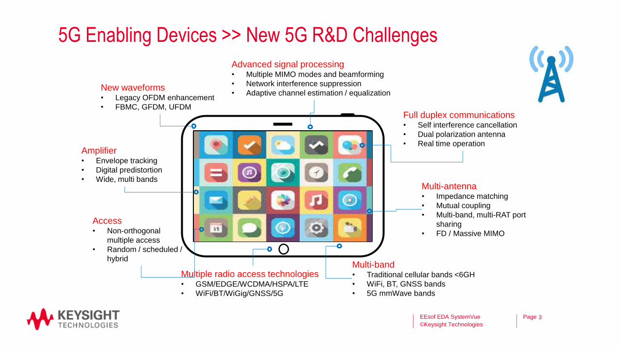
5G Enabling Devices >> New 5G R&D Challenges
EEsof EDA SystemVue
©Keysight Technologies
3
Multi-band • Traditional cellular bands <6GH
• WiFi, BT, GNSS bands
• 5G mmWave bands
Multi-antenna • Impedance matching
• Mutual coupling
• Multi-band, multi-RAT port
sharing
• FD / Massive MIMO
Amplifier • Envelope tracking
• Digital predistortion
• Wide, multi bands
Multiple radio access technologies • GSM/EDGE/WCDMA/HSPA/LTE
• WiFi/BT/WiGig/GNSS/5G
Advanced signal processing • Multiple MIMO modes and beamforming
• Network interference suppression
• Adaptive channel estimation / equalization
Full duplex communications • Self interference cancellation
• Dual polarization antenna
• Real time operation
New waveforms • Legacy OFDM enhancement
• FBMC, GFDM, UFDM
Access • Non-orthogonal
multiple access
• Random / scheduled /
hybrid

Page
5G Wireless: Opportunities to Innovate
EEsof EDA SystemVue
©Keysight Technologies
4
Why this will be exciting to us:
1 GHz 10 GHz 100 GHz 1 THz 10 THz 100 THz 1PHz
10 cm 1 cm 1 mm 100 mm 10 mm 1 mm
Wavelength Frequency
Microwave mm-Wave THz Far IR Infrared UV
100X Efficiency (energy/bit)
Reliability 99.999%
1mS Latency
100X Densification
1000X Capacity
100X Data Rates
Enabling Technologies
1. mmWave (Carrier, BW, MU-MIMO)
2. New <6GHz PHY/MAC
3. Full Duplex
4. >>400GB/s Fiber
5. Hyper-Fast Data Buses
6. C-RAN & New NW Topology

Page
Link Level Simulation Challenges & Revolutions
EEsof EDA SystemVue
©Keysight Technologies
5
Single-user Single-cell
Multi-user Single-cell
Multi-user Multi-cell
Multi-hierarchical relaying and coordination
GSM UMTS HSPA LTE/LTE-A
5G
3G • Synchronous dataflow technique
• Manual coding style language
4G • Dynamic dataflow technique
• Graphical design language
5G • Scenario aware dynamic
dataflow technique
• Graphical design +
scripting
• Incorporating data from
other sources
DB
PHY
Tx/Rx
chain 1
Link level simulator
PHY
Tx/Rx
chain 1
PHY
Tx/Rx
chain 1
System level simulator
PHY Parameters Interface
Scenario , Scripting , Control

Page
What you need for your research is…
5G New PHY Design and Test
©2014 Keysight Technologies
6
Transition naturally from Design to Test with a single “cockpit”
System Level
Platform
Software
Quickly capture “system level”
design concepts
Model implementation-level
impairments
Connect BB, RF, and T&M
for rapid validation
Rapid prototyping with
integrated measurement
RF / Analog
Channel Modeling MIMO Channel (OTA)
Digital Pre-Distortion (DPD)
RF System Design
Test Equipment RF Sources & Analyzers
AWG & Digitizers
Scopes, Logic, Modular
Test Software I/O Lib, ComExpert
89600 VSA
Signal Studio
3rd Party
BB Algorithm
Modeling MATLAB .m
FixedPoint, HDL/FPGA
Embedded C++
Filtering, EQ, Modem
IP Reference Libraries 4G LTE-Advanced, LTE ,5G
3G HSPA+, WCDMA, EDGE, GSM
WLAN 802.11ac/n/a/b/g
WPAN 802.11ad, 802.15.3c
RF EDA
Platforms
Mixed Simulation
Technologies
“Event Driven” plus
“Data Flow”
Page
Modeling New Physical Layer
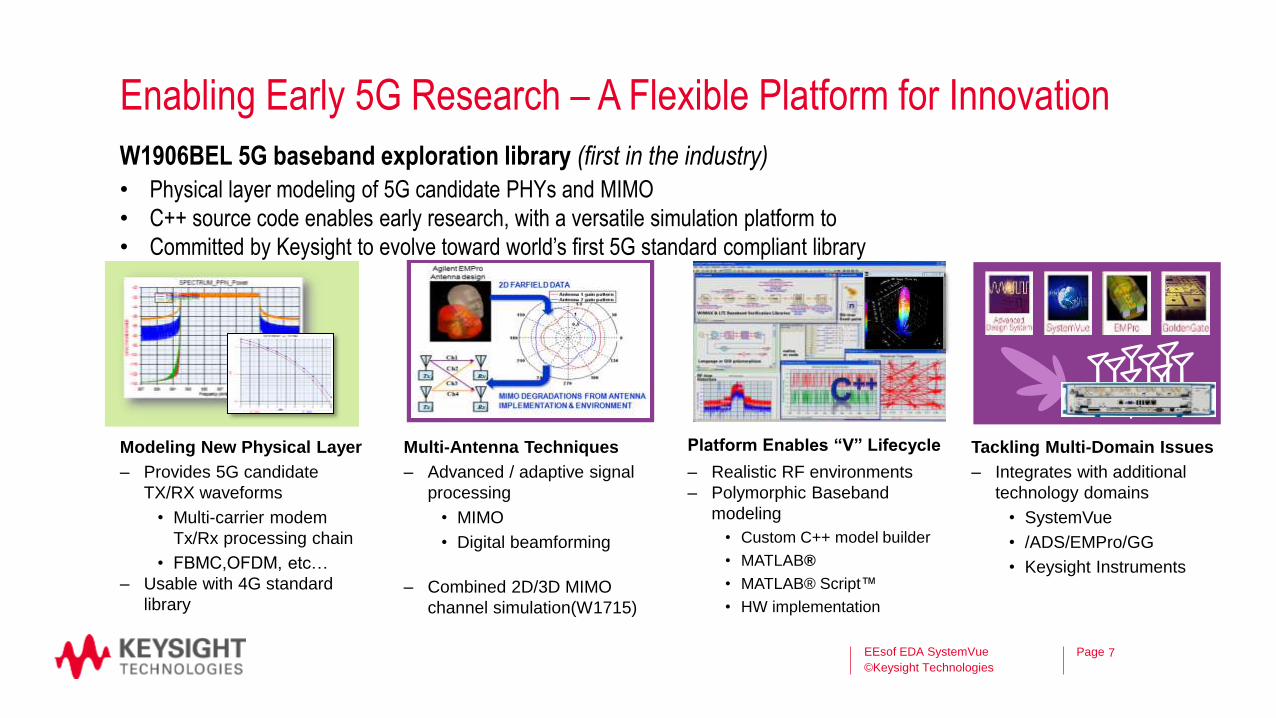
Enabling Early 5G Research – A Flexible Platform for Innovation
W1906BEL 5G baseband exploration library (first in the industry)
• Physical layer modeling of 5G candidate PHYs and MIMO
• C++ source code enables early research, with a versatile simulation platform to
• Committed by Keysight to evolve toward world’s first 5G standard compliant library
EEsof EDA SystemVue
©Keysight Technologies
7
Multi-Antenna Techniques Platform Enables “V” Lifecycle
– Provides 5G candidate
TX/RX waveforms
• Multi-carrier modem
Tx/Rx processing chain
• FBMC,OFDM, etc…
– Usable with 4G standard
library
– Advanced / adaptive signal
processing
• MIMO
• Digital beamforming
– Combined 2D/3D MIMO
channel simulation(W1715)
– Realistic RF environments
– Polymorphic Baseband
modeling
• Custom C++ model builder
• MATLAB®
• MATLAB® Script™
• HW implementation
Tackling Multi-Domain Issues
– Integrates with additional
technology domains
• SystemVue
• /ADS/EMPro/GG
• Keysight Instruments

5G New Waveform Techniques
Keysight EEsof EDA
November 14, 2014

Page
Waveform Design Considerations for 5G
EEsof EDA SystemVue
©Keysight Technologies
2
Bandwidth /
Frequency
Waveform
New RAT
3GHz 10GHz 30GHz 90GHz
Advanced Multi-Carrier Waveforms1
OFDM FBMC / OFDM / Others Single carrier
>> Wider BW, Higher Fc, much sensitive at phase noise
Note1: • Orthogonal Frequency Division Multiplexing(OFDM)
• Filter Bank Multicarrier(FBMC)
• Universal Filtered Multicarrier(UFMC)
• Generalized Frequency Division Multiplexing(GFDM)
• Biorthogonal Frequency Division Multiplexing(BFDM)
OFDMA NOMA SCMA

Page
Waveform Requirements
• Efficiently support high density users
• Optimized multiple access
• Carrier assignment schemes in asynchronous context
• Efficient usage of the allocated spectrum
• Robustness to narrow-band jammers and impulse noise
• High performance spectrum sensing
• Low computational complexity
• Compatibility OFDM vs. NEW
EEsof EDA SystemVue
©Keysight Technologies
3
Figure 1.
– OFDM vs. FBMC
Spectrum Using
different filter overlap
factor
Figure 2.
– FBMC Fragmented
Spectrum
Figure 3.
– UFMC multiplex of
sub-bands

Page
Filter Operation
EEsof EDA SystemVue
©Keysight Technologies
4
^ ^ ^ ^ ^ ^ ^ ^ ^ ^ ^ ^ ^ ^ ^ ^
UFMC
OFDM
FBMC
per sub-band
per full-band
per sub-carrier

Page
UFMC - Universal Filtered Multi-Carrier
EEsof EDA SystemVue
©Keysight Technologies
5
𝑤ℎ𝑒𝑟𝑒: N : FFT size, L : Filter length, ni : Complex QAM symbol F𝑖, 𝑘 𝑖𝑠 𝑎 𝑇𝑜𝑒𝑝𝑙𝑖𝑡𝑧 𝑚𝑎𝑡𝑟𝑖𝑥, 𝑐𝑜𝑚𝑝𝑜𝑠𝑒𝑑 𝑜𝑓 𝑡ℎ𝑒 𝑓𝑖𝑙𝑡𝑒𝑟 𝑖𝑚𝑝𝑢𝑙𝑠𝑒 𝑟𝑒𝑠𝑝𝑜𝑛𝑠𝑒 V𝑖, 𝑘 𝑖𝑠 𝑎 𝐼𝐷𝐹𝑇 𝑚𝑎𝑡𝑟𝑖𝑥, 𝑎𝑐𝑐𝑜𝑟𝑑𝑖𝑛𝑔 𝑡𝑜 𝑡ℎ𝑒 𝑟𝑒𝑠𝑝𝑒𝑐𝑡𝑖𝑣𝑒 𝑠𝑢𝑏 − 𝑏𝑎𝑛𝑑 𝑝𝑜𝑠𝑖𝑡𝑖𝑜𝑛 S𝑖, 𝑘 𝑖𝑠 𝑎 𝑠𝑦𝑚𝑏𝑜𝑙 𝑚𝑎𝑡𝑟𝑖𝑥
* OFDM can be implemented by set L as 1
𝑋𝑘 = 𝐹𝑖, 𝑘
𝑁𝑆𝐵
𝑖=1
𝑉𝑖, 𝑘 𝑆𝑖, 𝑘
[ 𝑁 + 𝐿 − 1 , 1] [ 𝑁 + 𝐿 − 1 , 𝑁] [𝑁, 𝑛𝑖] [𝑛, 1]
x
+
𝑉1
x
.
.
.
.
.
.
𝐹1
𝑆1
x
𝑉2
x
𝐹2
𝑆2
x
𝑉𝑁𝑆𝐵
x
𝐹𝑁𝑆𝐵
𝑆𝑁𝑆𝐵
P/S , IFFT Sub-band block
filtering
Figure 1.
Five sub-band multiplexed
Page
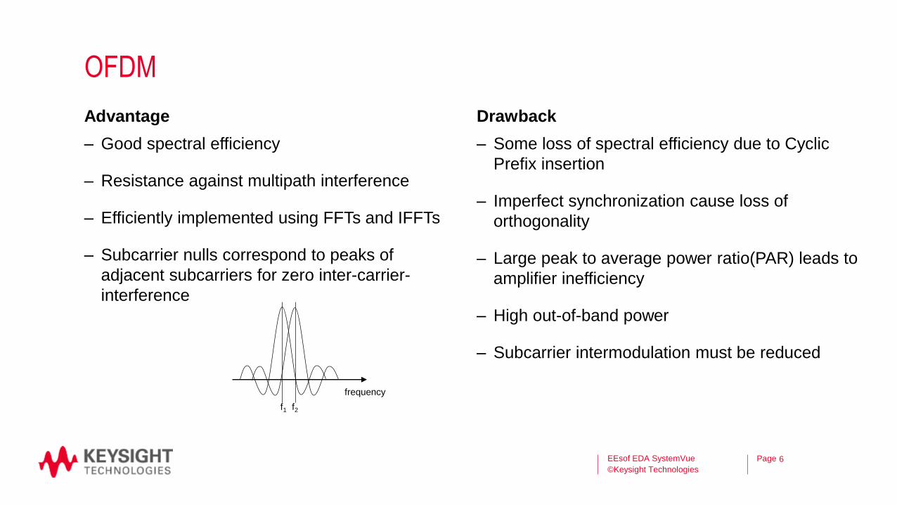
OFDM
Advantage
– Good spectral efficiency
– Resistance against multipath interference
– Efficiently implemented using FFTs and IFFTs
– Subcarrier nulls correspond to peaks of
adjacent subcarriers for zero inter-carrier-
interference
Drawback
– Some loss of spectral efficiency due to Cyclic
Prefix insertion
– Imperfect synchronization cause loss of
orthogonality
– Large peak to average power ratio(PAR) leads to
amplifier inefficiency
– High out-of-band power
– Subcarrier intermodulation must be reduced
EEsof EDA SystemVue
©Keysight Technologies
6
frequency
f1 f2

Page
OFDM vs. FBMC
EEsof EDA SystemVue
©Keysight Technologies
7
IFF
T
P / S
S / P
FF
T
Sym
bo
l
ma
pp
ing
Sub-c
arr
ier
ma
pp
ing
Sub-c
arr
ier
de-m
ap
pin
g
Sym
bo
l
de-m
ap
pin
g
OFDM baseband signal processing blocks
OQ
AM
pre
pro
cessin
g
IFF
T
Po
ly P
ha
se
Ne
two
rk
P / S
S / P
Po
ly P
ha
se
Ne
two
rk
FF
T
OQ
AM
p
ost p
roce
ssin
g
Synthesis Filter bank Analysis Filter bank
Sym
bo
l
ma
pp
ing
Sub
-ca
rrie
r
ma
pp
ing
Sub
-ca
rrie
r
de
-ma
pp
ing
Sym
bo
l
de
-ma
pp
ing
FBMC baseband signal processing blocks

Page
FBMC Signal Processing Block
EEsof EDA SystemVue
©Keysight Technologies
8
Staggering Transform Poly phase
filtering
P/S
Conversion
𝑧−1
𝑧−1
.
.
.
↓ 𝑀/2
↓ 𝑀/2
↓ 𝑀/2
𝐵0(𝑧2)
𝐵1(𝑧2)
𝐵𝑀 − 1(𝑧2)
𝑭𝑭𝑻
𝛽 0, 𝑛
𝛽 1, 𝑛
𝛽 𝑀 − 1, 𝑛
x
x
x
.
.
.
𝑆𝑢𝑏𝐶𝐻 Proc
𝑆𝑢𝑏𝐶𝐻 Proc
𝑆𝑢𝑏𝐶𝐻 Proc
𝜃 0, 𝑛
𝜃 1, 𝑛
𝜃 𝑀 − 1, 𝑛
x
x
x
𝑑 0, 𝑛
𝑑 1, 𝑛
𝑑 𝑀 − 1, 𝑛
.
.
.
𝑅𝑒
𝑅𝑒
𝑅𝑒
𝑅2𝐶𝑘
𝑅2𝐶𝑘
𝑅2𝐶𝑘
.
.
.
.
.
.
𝐴0(𝑧2)
𝛽0, 𝑛
𝛽1, 𝑛
𝛽𝑀 − 1, 𝑛
𝐴1(𝑧2)
𝐴𝑀 − 1(𝑧2)
↑ 𝑀/2
↑ 𝑀/2
↑ 𝑀/2
x +
𝑧−1
+
𝑧−1
𝑰𝑭𝑭𝑻
x
x
𝜃0, 𝑛
𝜃1, 𝑛
𝜃𝑀 − 1, 𝑛
x
x
x
𝐶2𝑅𝑘
𝑑0, 𝑛
𝐶2𝑅𝑘
𝐶2𝑅𝑘
𝑑1, 𝑛
𝑑𝑀 − 1, 𝑛
.
.
.
.
.
.
.
.
.
.
.
.
𝑠[𝑚]
.
.
.
S/P
Conversion
Poly phase
filtering Transform De-
staggering
Sub
channel
processing
OQAM pre-
processing Synthesis Filter Bank Analysis Filter Bank OQAM post-
processing
FBMC transmitter FBMC receiver

Page
OQAM Preprocessing
EEsof EDA SystemVue
©Keysight Technologies
9
𝑅(. )
𝑗𝐼(. )
↑ 2
↑ 2
+
𝑧−1
𝑥𝑘 𝑛
𝑐𝑘 𝑙
𝑅(. )
𝑗𝐼(. )
↑ 2
↑ 2
+
𝑧−1 𝑐𝑘 𝑙
= 1, 𝑗, 1, 𝑗, 1, . .
x
x
= 𝑗, 1, 𝑗, 1, 𝑗. .
• A time offset of half a QAM symbol period(T/2) is applied to either the real part or the
imaginary part of the QAM symbol
• For two successive sub-channels, say m and m+1, the offset are applied to the real part of
the QAM symbol in sub-channel , while it is applied to the imaginary part of the QAM
symbol in sub-channel m+1.
𝜃𝑘 𝑛
𝜃𝑘 𝑛
𝑥𝑘 𝑛
𝑑𝑘 𝑛
𝑑𝑘 𝑛
𝑓𝑜𝑟 𝑘 𝑒𝑣𝑒𝑛
𝑓𝑜𝑟 𝑘 𝑜𝑑𝑑
𝑐𝑜𝑚𝑝𝑙𝑒𝑥 𝑡𝑜 𝑟𝑒𝑎𝑙 𝑐𝑜𝑛𝑣𝑒𝑟𝑠𝑖𝑜𝑛 𝜃 pattern 𝑚𝑢𝑙𝑡𝑖𝑝𝑙𝑖𝑐𝑎𝑡𝑖𝑜𝑛

Page
Synthesis Filter Bank
EEsof EDA SystemVue
©Keysight Technologies
10
𝑠 𝑚 = 𝐴0(𝑧2)
𝛽0, 𝑛
𝛽1, 𝑛
𝐴1(𝑧2)
↑ 𝑀/2
↑ 𝑀/2
x +
𝑧−1
+ 𝑰𝑭𝑭𝑻
x
𝜃0, 𝑛
𝜃1, 𝑛
x
x
𝑑0, 𝑛
𝑑1, 𝑛
.
.
.
.
.
.
.
.
.
.
.
.
.
.
.
𝑤ℎ𝑒𝑟𝑒: M is number of subcarriers 𝑑𝑘, 𝑛 𝑖𝑠 𝑡ℎ𝑒 𝑟𝑒𝑎𝑙 𝑣𝑎𝑙𝑢𝑒𝑑 𝑠𝑦𝑚𝑏𝑜𝑙
𝜃𝑘, 𝑛 𝑖𝑠 𝑗
(𝑘 + 𝑛)
𝑔𝑘(m) is impulse response of the filters
* Filter overlap factor K : number of multicarrier symbols which
overlap in the time domain.
* OFDM can be implemented by set K as 1
.
𝑀−1
𝑘=0
𝑑𝑘, 𝑛
∞
𝑛=−∞
𝜃𝑘, 𝑛 𝑔𝑘 𝑚 − 𝑛𝑀/2
𝑠 𝑚

Page
Sub-channel Equalization
EEsof EDA SystemVue
©Keysight Technologies
11
Maximal ratio combined diversity reception
X
𝑍-1
X
𝑍-1
+
X
+
𝑦[𝑘]
𝑤0 𝑤1 𝑤2
t[𝑘] transmitted
symbol
Channel
Estimation H[z]
3-tap Complex FIR frequency sampling-design
𝑤i
Evaluation of MRC weighted target values
distorted subcarrier
sequence 𝑙 = number of tap
𝑣𝑘 𝑛 = 𝑤𝑘, 𝑙, 𝑛
2
𝑙=0
𝑦𝑘 𝑛 − 𝑙
𝑣𝑘 𝑛

Page
OQAM post processing
EEsof EDA SystemVue
©Keysight Technologies
12
↓ 2
𝑧−1
𝑧−1
↓ 2
+
𝑗
𝑥𝑘 𝑛 𝑐 𝑘 𝑙
↓ 2
𝑧−1
𝑧−1
↓ 2
+
𝑗 𝑐 𝑘 𝑙
x
x
𝜃 𝑘 𝑛
𝜃 𝑘 𝑛
𝑥𝑘 𝑛
𝑑 𝑘 𝑛
𝑑 𝑘 𝑛
𝑓𝑜𝑟 𝑘 𝑒𝑣𝑒𝑛
𝑓𝑜𝑟 𝑘 𝑜𝑑𝑑
𝑟𝑒𝑎𝑙 𝑡𝑜 𝑐𝑜𝑚𝑝𝑙𝑒𝑥 𝑐𝑜𝑛𝑣𝑒𝑟𝑠𝑖𝑜𝑛 𝜃 pattern 𝑚𝑢𝑙𝑡𝑖𝑝𝑙𝑖𝑐𝑎𝑡𝑖𝑜𝑛
𝑅(. )
𝑅(. )
Page
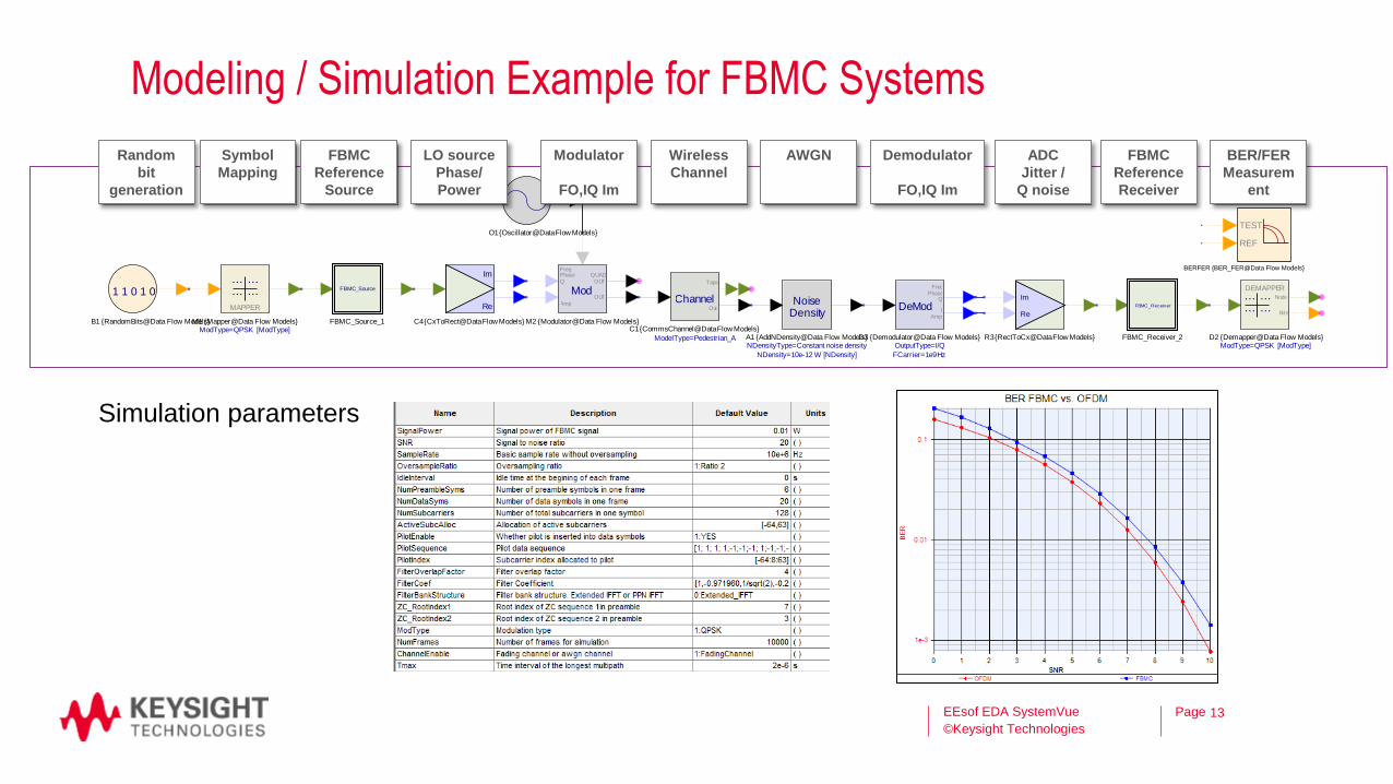
Modeling / Simulation Example for FBMC Systems
EEsof EDA SystemVue
©Keysight Technologies
13
Simulation parameters
ChannelOut
Taps
ModelType=Pedestrian_A
C1 {CommsChannel@Data Flow Models}
• • •• • •
• • • • • •
MAPPER
ModType=QPSK [ModType]M1 {Mapper@Data Flow Models}
1 1 0 1 0
B1 {RandomBits@Data Flow Models}
DeMod IAmp
FreqPhase
Q
FCarrier=1e9 Hz
OutputType=I/Q D3 {Demodulator@Data Flow Models}
• • •• • •
• • • • • •
DEMAPPER
Bits
Node
ModType=QPSK [ModType]D2 {Demapper@Data Flow Models}
FBMC_Source
FBMC_Source_1
Re
Im
C4 {CxToRect@Data Flow Models}
ModOUT
QUADOUT
FreqPhaseQ
IAmp
M2 {Modulator@Data Flow Models}Re
Im
R3 {RectToCx@Data Flow Models}
NoiseDensity
NDensity=10e-12 W [NDensity]
NDensityType=Constant noise density A1 {AddNDensity@Data Flow Models}
FBMC_Receiver
FBMC_Receiver_2
O1 {Oscillator@Data Flow Models}
Random
bit
generation
Symbol
Mapping
FBMC
Reference
Source
LO source
Phase/
Power
Modulator
FO,IQ Im
Wireless
Channel
AWGN
Demodulator
FO,IQ Im
FBMC
Reference
Receiver
BER/FER
Measurem
ent
TEST
REF
BERFER {BER_FER@Data Flow Models}
ADC
Jitter /
Q noise

Page
Reference Transmitter
EEsof EDA SystemVue
©Keysight Technologies
14
Pilot Insertion
Active Subcarriers Mapping Complex Splitter
Extend IFFT
PPN IFFT
OQAM Modulator Add IdleInterval
Bus=NO
Data Type=Complex Input {DATAPORT}
Preamble Sequence
OFDM _Subc arrierM ux
Input
Output
EVM Ref
CustomEVMRef=NO OversampleRatio=x2 [OFDMMuxOversampleRatio]
OutputOrder=Neg_DC_Pos In1_CarrierIndex=(1x128) [-64,-63,-62…
In1_DimCarrierIndex=1-D In1_NumCarriers=128 [[NumActiveSubc]]
NumInput=1 DFTSize=128 [NumSubcarriers]
O1
A
BlockSizes=(3x1) [6144; 20480; 3072] A1 {AsyncCommutator@Data Flow Models}
0
Value=0 C2 {Const@Data Flow Models}
0
Value=0 C3 {Const@Data Flow Models}
Bus=NO Data Type=Complex Output {DATAPORT}
T
SampleRate=20e+6 Hz [SampleRate*(2^OversampleRatio)]S1 {SetSampleRate@Data Flow Models}
A
BlockSizes=(3x1) [6144; 20480; 3072] A2 {AsyncCommutator@Data Flow Models}
OFDM _Subc arrierM ux
Input
Output
EVM Ref
CustomEVMRef=NO OversampleRatio=x2 [OFDMMuxOversampleRatio]
OutputOrder=Neg_DC_Pos In1_CarrierIndex=(1x128) [-64,-63,-62…
In1_DimCarrierIndex=1-D In1_NumCarriers=128 [[ActiveData]]NumInput=1 [DataSym_NumInput]DFTSize=128 [NumSubcarriers]
O2
FBM C_Ex tended_IFFT
Q_Out
I_Out
Q_In
I_In
ActiveSubcAlloc=(1x2) [-64,63] FilterCoef=(1x4) [1,-0.972,0.707,-0.2…
FilterOverlapFactor=4 NumSubcarriers=128 [NumSubcarriers]
OversampleRatio=Ratio 2 FBMC_Extended_IFFT_1
FBMC_PPN_IFFT
Output_Q
Ouput_I
Q
I
ActiveSubcAlloc=(1x2) [-64,63] FilterCoef=(1x4) [1,-0.972,0.707,-0.2…
FilterOverlapFactor=4 NumSubcarriers=128 [NumSubcarriers]OversampleRatio=1 [OversampleRatio]
Disabled: OPENFBMC_PPN_IFFT_1
FBMC_PPN_IFFT
Output_Q
Ouput_I
Q
I
ActiveSubcAlloc=(1x2) [-64,63] FilterCoef=(1x4) [1,-0.972,0.707,-0.2…
FilterOverlapFactor=4 NumSubcarriers=128 [NumSubcarriers]OversampleRatio=1 [OversampleRatio]
Disabled: OPEN
FBMC_PPN_IFFT_2
FBM C_Com plexSplitter
I
Q
input
ShiftPhase=NO FBMC_ComplexSplitter_1
FBMC
ZC Generator
ZC_RootIndex2=3 [ZC_RootIndex2]ZC_RootIndex1=7 [ZC_RootIndex1]
ActiveSubcAlloc=(1x2) [-64,63] NumActiveSubcarriers=128
NumSubcarriers=128 [NumSubcarriers]F1 {FBMC_ZC_Generator@5G Advanced Modem Models}
FBM C_OQAM _Modulator
Output
I
Q
FilterOverlapFactor=4 OversampleRatio=1 [OversampleRatio]NumSubcarriers=128 [NumSubcarriers]
FBMC_OQAM_Modulator_1
FBM C_Com plexSplitter
I
Q
input
ShiftPhase=YES
FBMC_ComplexSplitter_2
FBM C_Ex tended_IFFT
Q_Out
I_Out
Q_In
I_In
ActiveSubcAlloc=(1x2) [-64,63]
FilterCoef=(1x4) [1,-0.972,0.707,-0.2… FilterOverlapFactor=4
NumSubcarriers=128 [NumSubcarriers]OversampleRatio=Ratio 2 FBMC_Extended_IFFT_2
Periodic=YES Offset=0 V
ExplicitValues=<empty> V [ActivePilotSequence]Disabled: OPEN
W5 {WaveForm@Data Flow Models}
nWrite=7464 [FrameSizeWithIdle]nRead=7424 [FrameSize]
C1 {Chop@Data Flow Models}
Data and Pilot Insertion
Preamble Pattern Insertion
IFFT
Mode change
(Extended /
PPN)
Data
Framing
OQAM
Modulation
Idle Interval
Insertion
Prototype filter using different filter overlap factor

Page
Reference Receiver
EEsof EDA SystemVue
©Keysight Technologies
15
Bus=NO
Data Type=Complex
Input {DATAPORT}
nWrite=128 [NumSubcarriers]
nRead=256 [NumSubcarriers*2^OversampleRatio]
C15 {Chop@Data Flow Models}
nWrite=128 [NumSubcarriers]
nRead=256 [NumSubcarriers*2^OversampleRatio]
C1 {Chop@Data Flow Models}
REPEAT
BlockSize=128 [NumSubcarriers]
NumTimes=30 [NumGuardRemove+NumDataSyms]
R1 {Repeat@Data Flow Models}
0
Value=0
C2 {Const@Data Flow Models}
I nput
O ut put
FFO Est
FBMC
FracFreq Est
NumDataSyms=20 [NumDataSyms]
NumPreambleSyms=6 [NumPreambleSyms]
NumSubcarriers=128 [NumSubcarriers]
FilterOverlapFactor=4
IdleInterval=2e-6 [IdleInterval]
SampleRate=10e+6 [SampleRate]
OversampleOption=Ratio 2
F4
I nput
Tim ingEst
I FO Est
FBMC
Frame Sync
ZC_RootIndex2=3 [ZC_RootIndex2]
ZC_RootIndex1=7 [ZC_RootIndex1]
NumDataSyms=20 [NumDataSyms]
NumPreambleSyms=6 [NumPreambleSyms]
NumSubcarriers=128 [NumSubcarriers]
FilterOverlapFactor=4
IdleInterval=2e-6 [IdleInterval]
SampleRate=10e+6 [SampleRate]
OversampleOption=Ratio 2
F5
FBM C_O Q AM _Dem odulator
I _O ut
Q _O ut
I nput
FilterOverlapFactor=4
NumSubcarriers=128 [NumSubcarriers]
OversampleRatio=Ratio 2
FBMC_OQAM_Demodulator_1 {FBMC_OQAM_Demodulator@5G Advanced Modem Models}
FBMC
Chan Equalizer
NumEqualizerTaps=One Tap
ActiveSubcAlloc=(1x2) [-64,63]
NumActiveSubcarriers=128
NumSubcarriers=128 [NumSubcarriers]
F1 {FBMC_ChannelEqualizer@5G Advanced Modem Models}
OFDM _GuardRemoveI nput O ut put
OversampleRatio=x1
CIRAdjust=0
GuardStuff=CyclicShift
PostfixSize=0 [[0]]
PrefixSize=1120 [[ActiveData*NumGuardRemove]]
DFTSize=2240 [ActiveData*NumDataSyms]
O2 {OFDM_GuardRemove@Data Flow Models}
FBM C_Com plexCom binerO ut put
I _In
Q _In
FBMC_ComplexCombiner_1
Timing & Frequency Synchronization Frame DemuxOQAM Demod
Channel Estimation
FFT
Channel Equalization Phase Tracking
FBM C_PhaseTr acking
Q _O ut put
I _O ut put
Q _I nput
I _I nput
ActivePilotSequence=(16x1) [1; 1; 1]
PilotLoc=(1x16) [-64,-56,-48,-40,-32]
NumSubcarriers=128 [NumSubcarriers]
F3
Subcarrier Demux
O FDM _Subcar r ier Dem ux
I nput O ut put
OversampleRatio=x1
InputOrder=Neg_DC_Pos
Out1_CarrierIndex=(1x112) [-63,-62,-6…
Out1_DimCarrierIndex=1-D
Out1_NumCarriers=112 [[ActiveData]]
NumOutput=1
DFTSize=128 [NumSubcarriers]
O3 {OFDM_SubcarrierDemux@Data Flow Models}
A
BlockSizes=(2x1) [7424; 256]
A1 {AsyncCommutator@Data Flow Models}
Bus=NO
Data Type=Complex
Output {DATAPORT}
FBM C_Ext ended_FFT
I _O ut
Q _O ut
I _In
Q _In
ActiveSubcAlloc=(1x2) [-64,63]
FilterCoef=(1x4) [1,-0.972,0.707,-0.2…
FilterOverlapFactor=4
NumSubcarriers=128 [NumSubcarriers]
OversampleRatio=Ratio 2
Disabled: OPEN
FBMC_Extended_FFT_1 {FBMC_Extended_FFT@5G Advanced Modem Models}
FBM C_PPN_FFT
I _O ut
Q _O ut
I _In
Q _In
ActiveSubcAlloc=(1x2) [-64,63]
FilterCoef=(1x4) [1,-0.972,0.707,-0.2…
FilterOverlapFactor=4
NumSubcarriers=128 [NumSubcarriers]
OversampleRatio=Ratio 2
FBMC_PPN_FFT_1 {FBMC_PPN_FFT@5G Advanced Modem Models}
FBMC
Demux Frame
FreqSync=Full freq compensation
NumDataSyms=20 [NumDataSyms]
NumPreambleSyms=6 [NumPreambleSyms]
NumSubcarriers=128 [NumSubcarriers]
FilterOverlapFactor=4
IdleInterval=2e-6 [IdleInterval]
SampleRate=10e+6 [SampleRate]
OversampleOption=Ratio 2
F2
FBMC
Chan Estimator
Tmax=200e-9 [Tmax]
ActiveSubcAlloc=(1x2) [-64,63]
SampleRate=10e+6 [SampleRate]
NumPreambleSyms=6 [NumPreambleSyms]
ZC_RootIndex2=3 [ZC_RootIndex2]
ZC_RootIndex1=7 [ZC_RootIndex1]
OversampleOption=Ratio 2
NumActiveSubcarriers=128
NumSubcarriers=128 [NumSubcarriers]
F8 {FBMC_ChannelEstimator@5G Advanced Modem Models}
Fractional
Frequency
Offset
Estimation
IFO &
Timing
Estimation
Frame De-
multiplexing Analysis
Filter Bank
Sub-channel
Equalization Phase
Tracking Preamble
Remove
Channel
Estimation
Block
Diagram
Modeling using graphical
simulation tool
Auto-
correlation
Cross-correlation
with local Zadoff-
Chu sequence
Preamble symbols
with frequency
compensated
Preamble based
channel estimation
Multi-tap
equalization
Use pilot in
data symbols

Page
//The peak of auto-correlation is chosen by the midpoint of the inputs which exceed the threshold //FFO is gotten by the angle of the peak std::vector<double> AutoCorr(m_FrameSizeWithIdle,0); double maxV = 0; for (int i = 0; i < m_FrameSizeWithIdle; ++i) { AutoCorr[i] = abs(corr(m_Buffer.begin()+m_FrameSizeWithIdle-2*m_SymSize+i+1,m_Buffer.begin()+m_FrameSizeWithIdle-m_SymSize+i+1,m_SymSize)); if (AutoCorr[i] > maxV) maxV = AutoCorr[i]; } double threshold = maxV*0.75; int low_idx = 0; int upper_idx = 0; for (int i = 0; i < m_FrameSizeWithIdle; ++i) { if (AutoCorr[i] > threshold) { low_idx = i; break; } } for (int i = 0; i < m_FrameSizeWithIdle; ++i) { if (AutoCorr[i] > threshold) upper_idx = i; } int peak_idx = (low_idx + upper_idx)/2; std::complex<double> peak_corr; peak_corr = corr(m_Buffer.begin()+m_FrameSizeWithIdle-2*m_SymSize+peak_idx+1,m_Buffer.begin()+m_FrameSizeWithIdle-m_SymSize+peak_idx+1,m_SymSize); m_FFOEst = atan2(peak_corr.imag(),peak_corr.real())/(2*PI);
Fractional Frequency Estimation
EEsof EDA SystemVue
©Keysight Technologies
16
Page
std::copy(m_Buffer.begin()+m_FrameSizeWithIdle,m_Buffer.end(),m_Buffer.begin()); for (int i = 0; i < m_FrameSizeWithIdle; ++i) m_Buffer[i+m_FrameSizeWithIdle] = Input[i]; std::vector<double> CrossCorr1(m_FrameSizeWithIdle); std::vector<double> CrossCorr2(m_FrameSizeWithIdle); for (int i = 0; i < m_FrameSizeWithIdle; ++i) { CrossCorr1[i] = abs(corr(m_Buffer.begin()+m_FrameSizeWithIdle-m_SymSize+i+1,m_ZC_ifft1.begin(),m_SymSize)); CrossCorr2[i] = abs(corr(m_Buffer.begin()+m_FrameSizeWithIdle-m_SymSize+i+1,m_ZC_ifft2.begin(),m_SymSize)); } // Variable definition intentionally removed IFOEst[0] = (idx2-idx1)/(m_ZC_RootIndex1-m_ZC_RootIndex2)/m_OversampleRatio; TimingEst[0] = (idx2*m_ZC_RootIndex1-idx1*m_ZC_RootIndex2)/(m_ZC_RootIndex1-m_ZC_RootIndex2)-(m_FilterOverlapFactor-1)*m_SymSize+1;
Frame Synchronization
EEsof EDA SystemVue
©Keysight Technologies
17
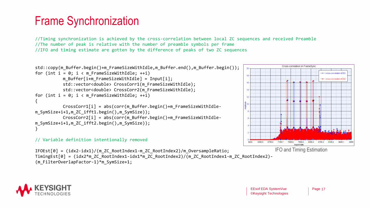
IFO and Timing Estimation
//Timing synchronization is achieved by the cross-correlation between local ZC sequences and received Preamble //The number of peak is relative with the number of preamble symbols per frame //IFO and timing estimate are gotten by the difference of peaks of two ZC sequences
Page
for (int i = 0; i< ActiveSubcAllocArraySize/2; i++) { std::vector<std::complex<double> > A, ANeg, APos; A.resize(ActiveSubcAlloc[2*i+1]-ActiveSubcAlloc[2*i]+1); ANeg.resize(ActiveSubcAlloc[2*i+1]-ActiveSubcAlloc[2*i]+1); APos.resize(ActiveSubcAlloc[2*i+1]-ActiveSubcAlloc[2*i]+1); for (int k = 0; k < ActiveSubcAlloc[2*i+1]-ActiveSubcAlloc[2*i]+1; k++) A[k] = tmp[ActiveSubcAlloc[2*i]+NumSubcarriers/2+k]; ANeg[0] = 0.5*(A[ActiveSubcAlloc[2*i+1]-ActiveSubcAlloc[2*i]] + A[0]); for (int k = 1; k < ActiveSubcAlloc[2*i+1]-ActiveSubcAlloc[2*i]+1; k++) { ANeg[k] = 0.5*(A[k-1] + A[k]); } for (int k = 0; k < ActiveSubcAlloc[2*i+1]-ActiveSubcAlloc[2*i]; k++) { APos[k] = 0.5*(A[k+1] + A[k]); } APos[ActiveSubcAlloc[2*i+1]-ActiveSubcAlloc[2*i]] = 0.5*(A[ActiveSubcAlloc[2*i+1]-ActiveSubcAlloc[2*i]] + A[0]); for (int k = 0; k < ActiveSubcAlloc[2*i+1]-ActiveSubcAlloc[2*i]+1; k++) { m_WNeg[ActiveSubcAlloc[2*i]+NumSubcarriers/2+k] = ANeg[k]; m_WPos[ActiveSubcAlloc[2*i]+NumSubcarriers/2+k] = APos[k]; m_W[ActiveSubcAlloc[2*i]+NumSubcarriers/2+k] = A[k]; } }
Channel Estimation and Equalization
EEsof EDA SystemVue
©Keysight Technologies
18
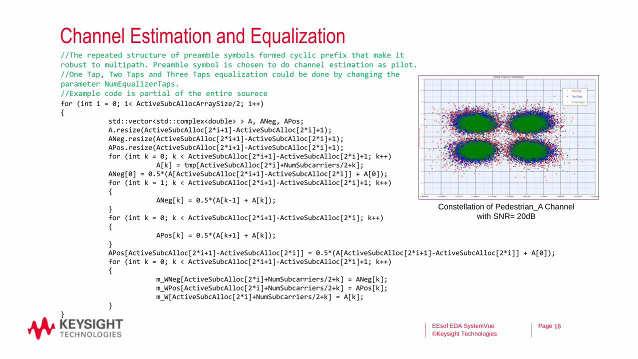
//The repeated structure of preamble symbols formed cyclic prefix that make it robust to multipath. Preamble symbol is chosen to do channel estimation as pilot. //One Tap, Two Taps and Three Taps equalization could be done by changing the parameter NumEqualizerTaps. //Example code is partial of the entire sourece
Constellation of Pedestrian_A Channel
with SNR= 20dB
Page
Performance Analysis with Real Hardware
EEsof EDA SystemVue
©Keysight Technologies
19
RFIC DUT
• Wider BW (63 GHz BW)
• Higher Sampling (160 GSa/s)
BBIQ - RF
RF - BBIQ
M8190A 12 GSa/S Arbitrary
Waveform Generator
M9703A AXIe 12-bit High-Speed
Digitizer/Wideband Digital Receiver
Interleaving to get 4ch @ 3.2 GSa/s
Infiniium 90000 Q-Series Oscilloscope
I
Q
I
Q
SYSTEMVUE
TEST
REF
BERFER {BER_FER@Data Flow Models}
BPSK, QPSK, ..., up to 4096-QAM
8-PSK, 16-PSK, 16-APSK, 32-APSK16-Star QAM, 32-Star-QAM,
and Custom APSK
Data PayloadPreambleIdle
Frame Structure
Spreading CodeGenerator
X
Digital Modem Sourcefor Linear Modulation
DSSS System
Payload_ModType=16-QAM [Payload_ModType]
Preamble_ModType=BPSK [Preamble_ModType]
Decision Device
FeedwardFilter
-
-
FeedbackFilter
Decision Feedback Equalizer
Fast Computation Algorithm
CIR--->DFE coefficients
Digital Modem Receiver
TrackingAlgorithm=LMS
FreqSync_Mode=CIR Corr
FrameSync_Algorithm=DiffCorr
{DigMod_ReceiverL_FastDFE}
Automatic waveform
creation & download
Reference Source
Reference
Receiver
BER/FER Measurement
Custom modem
design
5G Reference
Library
: Replaceable
in C++, .m or
SV DSP
parts formats

MIMO and Digital Beamforming
Keysight EEsof EDA
November xx, 2014

Page
Motivation
– Higher requirement for system capacity and spectral efficiency(bits/s/Hz)
– To overcome traditional approaches ( expand bandwidth, higher modulation order,
multiple access)
– The MIMO for better use the spatial resource
• The capacity is increased by a multiplication of the number of antennas
EEsof EDA SystemVue
©Keysight Technologies
2
MsbitN
SBC
/1log2

Page
Classification
EEsof EDA SystemVue
©Keysight Technologies
3
Spatial diversity
Improve robustness
Transmit Diversity Receive Diversity
Space-time block coding (STBC)
X1, X2
-X2, X1*
y1, y2
Spatial division multiplexing
Transmit Beamforming
Spatial multiplexing
Improve user throughput
MIMO
Matrix
X1
X2
y1
y2
Spatial Expansion
Multi-user MIMO
Multi-user Increase system
efficiency
Multi streams/users
.
.
.
.
.
. M a
nte
nn
as
K t
erm
inals
S s
tre
am
s
Massive MIMO
M >> K >> 1
Massive multi-users
Use spatial channel
information? • Open-loop MIMO
• Closed-loop MIMO
Page
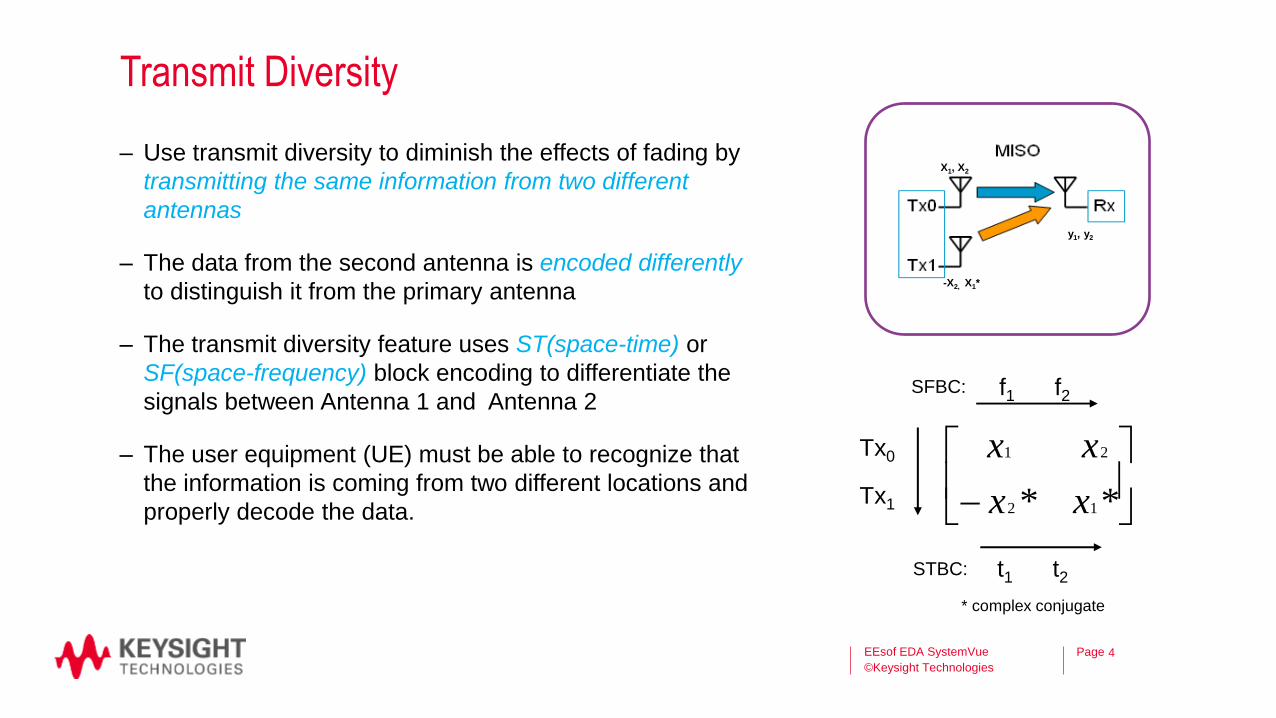
Transmit Diversity
– Use transmit diversity to diminish the effects of fading by
transmitting the same information from two different
antennas
– The data from the second antenna is encoded differently
to distinguish it from the primary antenna
– The transmit diversity feature uses ST(space-time) or
SF(space-frequency) block encoding to differentiate the
signals between Antenna 1 and Antenna 2
– The user equipment (UE) must be able to recognize that
the information is coming from two different locations and
properly decode the data.
EEsof EDA SystemVue
©Keysight Technologies
4
X1, X2
-X2, X1*
y1, y2
** 12
21
xx
xx
f1 f2
t1 t2
Tx0
Tx1
SFBC:
STBC:
* complex conjugate

Page
Spatial Multiplexing
– Operation Concept
• Transmission of multiple spatial data streams over
different antennas in the same RB
• The dimension of spatial channels is increased and
system capacity increased
– Relevant signal processing
• Perform Layer mapping and Pre-coding to lower the
receiver complexity and reduce the signal interference
between antennas
• Statistic correlation between vector(h11,h12) and
vector(h21,h22 )
EEsof EDA SystemVue
©Keysight Technologies
5
X1
X2
y1
y2
h11
h21
h12
h22
x: transmitted signal,
y: received signal,
H: spatial channel matrix,
Hij: channel coefficient from the jth transmit
antenna and the ith receive antenna.
y=Hx
y1=h11x1+h12x2+n1
y2=h21x1+h22x2+n2

Page
Modeling and Simulation for MIMO
– MIMO Tx/Rx simulation under Rayleigh fading and AWGN channel
– Explore different decoding algorithms and performance evaluation
• ML, MMSE-SIC, ZF-SIC, MMSE-Linear, ZF-Linear
EEsof EDA SystemVue
©Keysight Technologies
6
A4 {Add@Data Flow Models}
StdDev=707.1e-6 V [StdDev]I2 {IID_Gaussian@Data Flow Models}
StdDev=707.1e-6 V [StdDev]I6 {IID_Gaussian@Data Flow Models}
Re
Im
R1 {RectToCx@Data Flow Models}
[ ]
Format=ColumnMajor NumCols=1 [RxNumCols]
NumRows=2 [RxNumRows]P2 {Pack_M@Data Flow Models}
[ ]
Format=ColumnMajor NumCols=1 [TxNumCols]
NumRows=2 [TxNumRows]
U1 {Unpack_M@Data Flow Models}
MIMO_DecoderRec ov eredData
M odType
ChannelRes ponse
Rec eiv edData
DebugFlag=0
ModType=QPSK [ModType]DecoderMethod=ML [DecoderMethod]
Mode=Spatial Multiplexing [Mode]M3 {MIMO_Decoder@5G Advanced Modem Models}
• • •• • •
• • • • • •
DEMAPPER
Bits
Node
ModType=QPSK [ModType]D1 {Demapper@Data Flow Models}
M2 {Mpy@Data Flow Models}
StdDev=0.707 V [1/sqrt(2)]I5 {IID_Gaussian@Data Flow Models}
Re
Im
R3 {RectToCx@Data Flow Models}
[ ]
Format=ColumnMajor
NumCols=2 [ChannelNumCols]NumRows=2 [ChannelNumRows]
P1 {Pack_M@Data Flow Models}
StdDev=0.707 V [1/sqrt(2)]I7 {IID_Gaussian@Data Flow Models}
MIMO_Encoder
NumTx=2 [NumTx]Mode=Spatial Multiplexing [Mode]
M1 {MIMO_Encoder@5G Advanced Modem Models}
[ ]
Format=ColumnMajor NumCols=1 [TxNumCols]
NumRows=2 [TxNumRows]P3 {Pack_M@Data Flow Models}
• • •• • •
• • • • • •
MAPPER
ModType=QPSK [ModType]
M5 {Mapper@Data Flow Models}
1 1 0 1 0
B2 {RandomBits@Data Flow Models}
Fading Channel AWGN
Transmit with MIMO coding MIMO decoding and demapper
Page
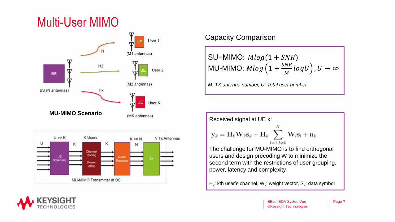
Multi-User MIMO
EEsof EDA SystemVue
©Keysight Technologies
7
Received signal at UE k:
The challenge for MU-MIMO is to find orthogonal
users and design precoding W to minimize the
second term with the restrictions of user grouping,
power, latency and complexity
Hk: kth user’s channel, Wk: weight vector, Sk: data symbol
SU−MIMO: 𝑀𝑙𝑜𝑔(1 + 𝑆𝑁𝑅)
MU-MIMO: 𝑀𝑙𝑜𝑔 1 +𝑆𝑁𝑅
𝑀𝑙𝑜𝑔𝑈 , 𝑈 → ∞
M: TX antenna number, U: Total user number
Capacity Comparison
MU-MIMO Scenario

Page
Multi-User MIMO
Advantages
– Maintain spatial multiplexing gain without large
antenna number at terminals
– Multiple access capacity gain (proportional to
BS antennas)
– More immune to propagation limitations such
as channel rank loss, antenna correlation and
LOS
Disadvantages
– BS needs to know channel state information at
transmitter (CSIT). The challenges include
• TDD vs. FDD for CSIT
• CSI feedback path bandwidth, Code book
design
– Complexity of the scheduling procedure at BS
• User grouping scheduling, power allocation
and latency requirements
EEsof EDA SystemVue
©Keysight Technologies
8

Page
Modeling and Simulation for Capacity Estimation
EEsof EDA SystemVue
©Keysight Technologies
9
Simulation condition
– Transmit antenna number (M) : 4
– Total number of user : from 4 to 100
– SNR=10dB
– Power allocation by waterfilling algorithm
User Scheduler
Power_Selected
W_Selected
H_Selected
H
TotalPower=10 [SNR]
NumRx=1
NumTx=4 [NumTx]
TotalUsers=100 [TotalUsers]
UserScheduler {MATLAB_Script@Data Flow Models}
Channel Capacity
R
P
W
H
NumRx=1
Noise=1
NumTx=4 [NumTx]
SumRate {MATLAB_Script@Data Flow Models}
NumInputsToAverage=100
A1 {Average@Data Flow Models}
123
StartStopOption=Samples
S4 {Sink@Data Flow Models}
StdDev=0.707 V [1/sqrt(2)]
I1 {IID_Gaussian@Data Flow Models}
StdDev=0.707 V [1/sqrt(2)]
I3 {IID_Gaussian@Data Flow Models}
Re
Im
R2 {RectToCx@Data Flow Models}
[ ]
Format=ColumnMajor
NumCols=4 [NumTx]
NumRows=1 [NumRx]P4 {Pack_M@Data Flow Models}
BlockSize=1
D2 {Distributor@Data Flow Models}
Channel transfer matrix User scheduling Capacity measurement
User K: 4->100
Su
m C
ap
acity

Page
Massive MIMO
– The use of a very large number of service antennas operated fully
coherent and adaptive
– Brings huge improvements in throughput and energy efficiency
when combined with simultaneous scheduling of a large number of
Ues
– System Model : M transmit antenna with maximum S streams, K
users each with a single antenna
– Originally envisioned for time division duplex(TDD1), but can
potentially be applied in frequency division duplex(FDD)
EEsof EDA SystemVue
©Keysight Technologies
10
.
.
.
.
.
. M a
nte
nn
as
K t
erm
ina
ls
S s
tre
am
s
Massive MIMO
M >> K >> 1
Massive multi-users
Note1 : Prefer TDD as not enough resources for pilots and CSI feedback.

Page
Massive MIMO Operation and Challenges
Operation
– Acquire Channel State Information from uplink
Pilots / Data
– Reciprocity calibration and adjustment
– Pre-coding1 to support multi-stream
transmission
– MMSE receiver with beamforming
• Maximum ratio combining(MRC) : interference
and noise are both white in the space
• Interference rejection combining(IRC): colored
interference
Challenges
– Pilot contamination: interference from other cells
• Blind channel estimation?
• Coordination and planning?
– New pre-coder with low-complexity, low-PAPR
– Hardware performance
• I/Q imbalance, A/D resolution, PA linearity
• Phase noise, clock distribution
– Synchronization at low SNR
– Understand mmWave MIMO channel
EEsof EDA SystemVue
©Keysight Technologies
11
Note1 : Linear pre-coding [maximum ratio transmission(MRT), zero-forcing(ZF)].
Non-linear pre-coding [Dirty paper coding(DPC)], full CSI required

Page
Modeling and Simulation for Large Number of Antennas
EEsof EDA SystemVue
©Keysight Technologies
12
quad_output
output
LO
inputMultiChannel
Modulator
ShowIQ_Impairments=NO MirrorSignal=NO
ConjugatedQuadrature=NO AmpSensitivity=1 [[1]]
InitialPhase=0 ° [[0]]FCarrier=1e6 Hz
NumChannels=1 M1 {MultiCh_Modulator@5G Advanced Modem Models}
TxBeamformer
weights
output
InPhi
InTheta
input
Phi=0 °Theta=0 °
Dy=0.5 Dx=0.5
NumOfAnty=4 NumOfAntx=4
BeamformingType=Calculate by antenna … T1 {Tx_Beamformer@5G Advanced Modem Models}
Env
OutputFc=Center
M4 {MultiCh_AddEnv@5G Advanced Modem Models}
MultiChNoise Density
NDensity=0.0 WNDensityType=Constant noise density
M6 {MultiCh_AddNDensity@5G Advanced Modem Models}
MultiChannel
Demodulator
ShowIQ_Impairments=NO MirrorSignal=NO
AmpSensitivity=1 [[1]]InitialPhase=0 ° [[0]]
FCarrier=1e6 HzNumChannels=1
M2 {MultiCh_Demodulator@5G Advanced Modem Models}
RxBeamformer
weights
output
ref
input
BlockSize=1024 ABF_Algorithm=Sample Matrix Inversion
NumOfTxAnts=16 R1 {Rx_Beamformer@5G Advanced Modem Models}
Power=.010 WFrequency=1000000 HzO1 {Oscillator@Data Flow Models}
Transmit
Beamformer
Multi-CH
Modulator
Multi-CH
Envelope Adder
Multi-CH
AWGN
Multi-CH
De-Modulator
Receive
Beamformer
Plotting • Antenna pattern review
• Interference analysis
between different
streams
• Beam pattern vs. pre-
coding analysis(MRT,ZF)
Scripting • Multiuser scheduling
• Capacity analysis
• Quick algorithm
implementation and test
• Calibration

Page
Channel Sounding / Parameter Extraction / Simulation
EEsof EDA SystemVue
©Keysight Technologies
13
𝑧[𝑘] t[𝑘]
Reference transmit signal(chirp/pn)
channel
H[z] ∑ CIR
correlation
Channel
impulse
response
Channel sounding
Estimation
algorithms
Channel
parameters
• PDP (Path delay, path loss)
• AOA, AOD
• Doppler shift
Parameters estimation
• Scenario selection
• Network layout
• Antenna parameters
Large/Small scale
parameters
generation
Fading coefficient
generation
• AS AoA/AoD
• PAS
• Doppler spectrum
• Correlation
• Rician K factor
Statistics & modeling
¤ 𝑥[𝑘] 𝑦[𝑘]
Input signal faded signal
SystemVue Simulation
SAGE
Maximum likelihood
estimation algorithm
No limitation for number
of path, suitable for both
LOS and NLOS scenarios
Can estimate all the
channel parameters
including path loss and path
delay of each path
Iteration needed, large
computing amount
ESPRIT
Subspace based algorithm
Maximum estimating
number of path is limited by
number of Rx, will be fail
under NLOS scenario
cannot estimate path loss
and path delay
small computing amount
Page
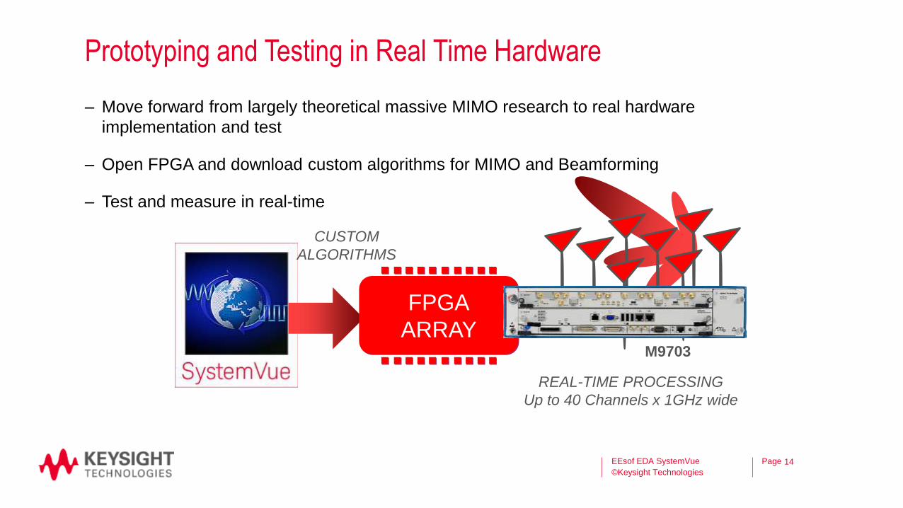
Prototyping and Testing in Real Time Hardware
EEsof EDA SystemVue
©Keysight Technologies
14
FPGA
ARRAY M9703
REAL-TIME PROCESSING
Up to 40 Channels x 1GHz wide
CUSTOM
ALGORITHMS
FPGA
ARRAY
– Move forward from largely theoretical massive MIMO research to real hardware
implementation and test
– Open FPGA and download custom algorithms for MIMO and Beamforming
– Test and measure in real-time

Tacking Cross Domain Issue
Keysight EEsof EDA
November xx, 2014

Page
Motivation
– Design problem spans to different technology domains (Baseband signal processing,
RF circuit design, Radio access networking)
– System level problem cannot be solved in any one domain alone
– RF circuit verification now needs using a realistic representation of the complex
modulated RF signal
– Baseband and RF team entirely isolated and use different type of tools
– Needs unified BB/RF design and verification flow
EEsof EDA SystemVue
©Keysight Technologies
2

Page
Modeling Transmitter Path
EEsof EDA SystemVue
©Keysight Technologies
3
Signal quality degraded by:
• PA Compression
• Intermods
• Spectral Spread
• LO Phase Noise
• BPF Filter Effects
Phase
Noise
ModOUT
QUAD
OUT
Freq
Phase
Q
I
Amp
FCarrier=897e6Hz
InputType=I/QM5 {Modulator@Data Flow Models}
Power=0.01WFrequency=897e+6Hz [Fcarrier]
O3 {Oscillator@Data Flow Models}
Amplifier
TOIout=10W
GCType=noneNoiseFigure=0
Gain=1GainUnit=voltage
A2 {Amplif ier@Data Flow Models}
Re
Im
Poly Phase
FBMC_Tx
OversampleRatio=2 [OversampleRatio]MappingType=5 [MappingType]
FilterCoef=(3x1) [-0.972; 0.707; -0.235…
FilterOverlapFactor=4ActiveSubcAlloc=(2x2) [-64,-31; 10,63]
NumSubc=128 [NumSubc]Subnetwork1 {PPN IFFT Transmitter}
1 1 0 1 0
Spectrum Analyzer
ResBW=5000HzStart=0s
Mode=ResBW
SPECTRUM_PPN {SpectrumAnalyzerEnv@Data Flow Models}
CCDF
Stop=2e-2sStart=0s
Distribution_PPN {CCDF_Env@Data Flow Models}PassRipple=1
PassBandwidth=100e6Hz
FCenter=897e+6Hz [Fcarrier]F1 {BPF_ChebyshevI@Data Flow Models}
Gain, NF &
Compression
Characteristics Ripple, Group
Delay & BPF
Characteristics
Signal quality degraded by:
• Different multi-carrier waveform
• Apply different prototype filter
Gain, phase
imbalance, IQ
offset
Different
waveform,
modulation

Page
Modeling Receiver Path
EEsof EDA SystemVue
©Keysight Technologies
4
NoiseDensity
NDensity=31.62e-12W [NDensity]
NDensityType=Constant noise density
A1 {AddNDensity@Data Flow Models}
DeModI
Amp
FreqPhase
Q
FCarrier=80e6Hz
OutputType=I/Q
D3 {Demodulator@Data Flow Models}
RF_Rx
Subnetwork3 {RF_Rx}
Re
Im
R3 {RectToCx@Data Flow Models}
FBMC_Rx
Poly Phase
OversampleRatio=2 [OversampleRatio]
MappingType=4 [MappingType]
FilterCoef=(3x1) [-0.972; 0.707; -0.235…
FilterOverlapFactor=4
ActiveSubcAlloc=(2x2) [-128,-1; 0,127]
NumSubc=256 [NumSubc]
Subnetwork2 {PPN FFT Receiver}
Bus=NO
Data Type=Envelope Signal
RF_Signal
Bus=NO
Data Type=Envelope Signal
BB_Signal {DATAPORT}
IN OUT
LO
TOIout=1.0e17W
SOIout=1.0e17W
Sideband=Lower
NoiseFigure=0 [NoiseFigure_Mixer]
EnableNoise=YES
ConvGain=0
M3
SampleRate=100e+6Hz [IF_SamplingRate]
Power=0dBm
Frequency=975e+6Hz [RF_Freq-IF_Freq]
O1
PassAtten=0.02
PassBandwidth=5e+6Hz [BandWidth]
FCenter=25e+6Hz [IF_Freq]
F1 {BPF_Butterworth@Data Flow Models}
Amplif ier
RefR=50Ω
GCType=none [GCType_IFGain]
NoiseFigure=0 [NoiseFigure_IFGain]
Gain=1 [IF_Gain]
A1
Amplif ier
RefR=50Ω
GCType=none [GCType_RFGain]
NoiseFigure=0 [NoiseFigure_RFGain]
Gain=1 [RF_Gain]
A2
LNA Characteristic
• Gain
• Noise Figure
• Compression
Phase
Noise
RF/Analog Modeled Effects
• Multipath
• Path Loss
• LNA NF
• LO Phase Noise
• ADC, Clock Jitter
BB Modeled Effects
• Baseband algorithm
performance Add
Noise
Page
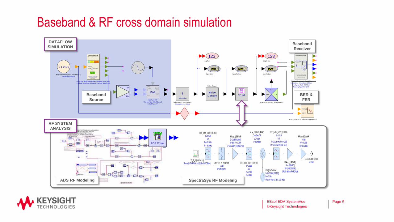
Baseband & RF cross domain simulation
EEsof EDA SystemVue
©Keysight Technologies
5
Spe c t rum A nalyzer
SpecRxIn
Spe c t rum A nalyzer
SpecRxOut
123SigRxIn
123SigRxOut
NoiseDensity
Noise_Power
Attenuation
Attenuation=54 [Atten]
Subnetwork1 {Attenuation}
1 1 0 1 0
DataPattern=PN15
B2 {DataPattern@Data Flow Models}
TEST
REF
BERFER {BER_FER@Data Flow Models}
Re
ImFc
CxEnv
E2 {EnvToCx@Data Flow Models}
Spe c t rum A nalyzer
SpecRxWnoi
ModOUT
QUADOUT
FreqPhaseQ
IAmp
InitialPhase=0°
FCarrier=81e+9Hz [FCarrier]
InputType=I/Q
RF_Link
SYS
BPSK, QPSK, ..., up to 4096-QAM8-PSK, 16-PSK, 16-APSK, 32-APSK
16-Star QAM , 32-Star-QAM, and Cus tom APSK
Data Pay loadPreambleId le
Fram e Struc ture
Spreading Code
Generator
X
D ig it a l M ode m Source
f o r L ine a r M odu lation
DSSS Sy s tem
Payload_ModType=16-QAM [Payload_ModType]
Preamble_ModType=BPSK [Preamble_ModType]
Dec ision
Dev ice
Feedward
Fi l ter-
-
Feedback
Fi l ter
Dec is ion Feedbac k Equal izer
Fas t Com putation Algori thm
CIR--->DFE c oeffic ients
D ig it a l M ode m R e ceiver
TrackingAlgorithm=LMS
FreqSync_Mode=CIR Corr
FrameSync_Algorithm=DiffCorr
{DigMod_ReceiverL_FastDFE}
Baseband
Source
Baseband
Receiver
BER &
FER
DATAFLOW
SIMULATION
R I
L
IP1dB=5dBmLO=7dBm
ConvGain=0dBMixer_1 {MIXER_BASIC}
PhaseN=(4) [-60; -80; -100; -96]dB
Pwr=7dBmF=60750MHz [3*FTXIF]LO7 {PwrOscillator}
Fhi=20375MHz [FTXIF+CS/2]
Flo=20125MHz [FTXIF-CS/2]N=3
IL=0.01dB
BPF_Butter_9 {BPF_BUTTER}
OP1dB=8dBm [RXIFOP1dB]NF=10dB [RXIFNF]
G=4dB [RXIFG]RFAmp_2 {RFAMP}
OP1dB=4dBm
NF=26.16dBG=0dB
RFAmp_5 {RFAMP}
ZO=50ΩRECEIVEROUT {*OUT}
Fhi=86.5GHz
Flo=80.5GHzN=5
IL=0.01dB
BPF_Butter_8 {BPF_BUTTER}
IP1dB=100dBm
L=1dBAttn_4 {ATTN_NonLinear}
Fhi=86GHzFlo=81GHz
N=3IL=0.01dB
BPF_Butter_6 {BPF_BUTTER}Source1=FTXRF MHz at -12 dBm, BW: CS MHzTX_IF_IN {MultiSource}
OP1dB=4dBm [RXLNAOP1dB]
NF=8dB [RXLNANF]G=22dB [RXLNAG]RFAmp_1 {RFAMP}
SpectraSys RF Modeling
RF SYSTEM
ANALYSIS
ADS Cosim
ADS RF Modeling
Page
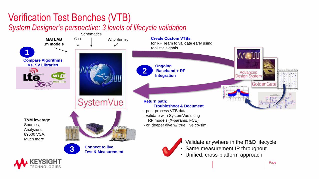
Verification Test Benches (VTB) System Designer’s perspective: 3 levels of lifecycle validation
Page 6
MATLAB
.m models
C++
Schematics
Waveforms
1 Compare Algorithms
Vs. SV Libraries
• Validate anywhere in the R&D lifecycle
• Same measurement IP throughout
• Unified, cross-platform approach 3 Connect to live
Test & Measurement
T&M leverage
Sources,
Analyzers,
89600 VSA,
Much more
Ongoing
Baseband + RF
Integration 2
Create Custom VTBs
for RF Team to validate early using
realistic signals
Return path:
Troubleshoot & Document
- post-process VTB data
- validate with SystemVue using
RF models (X-params, FCE)
- or, deeper dive w/ true, live co-sim
EEsof EDA SystemVue ©Keysight
Technologies
Page
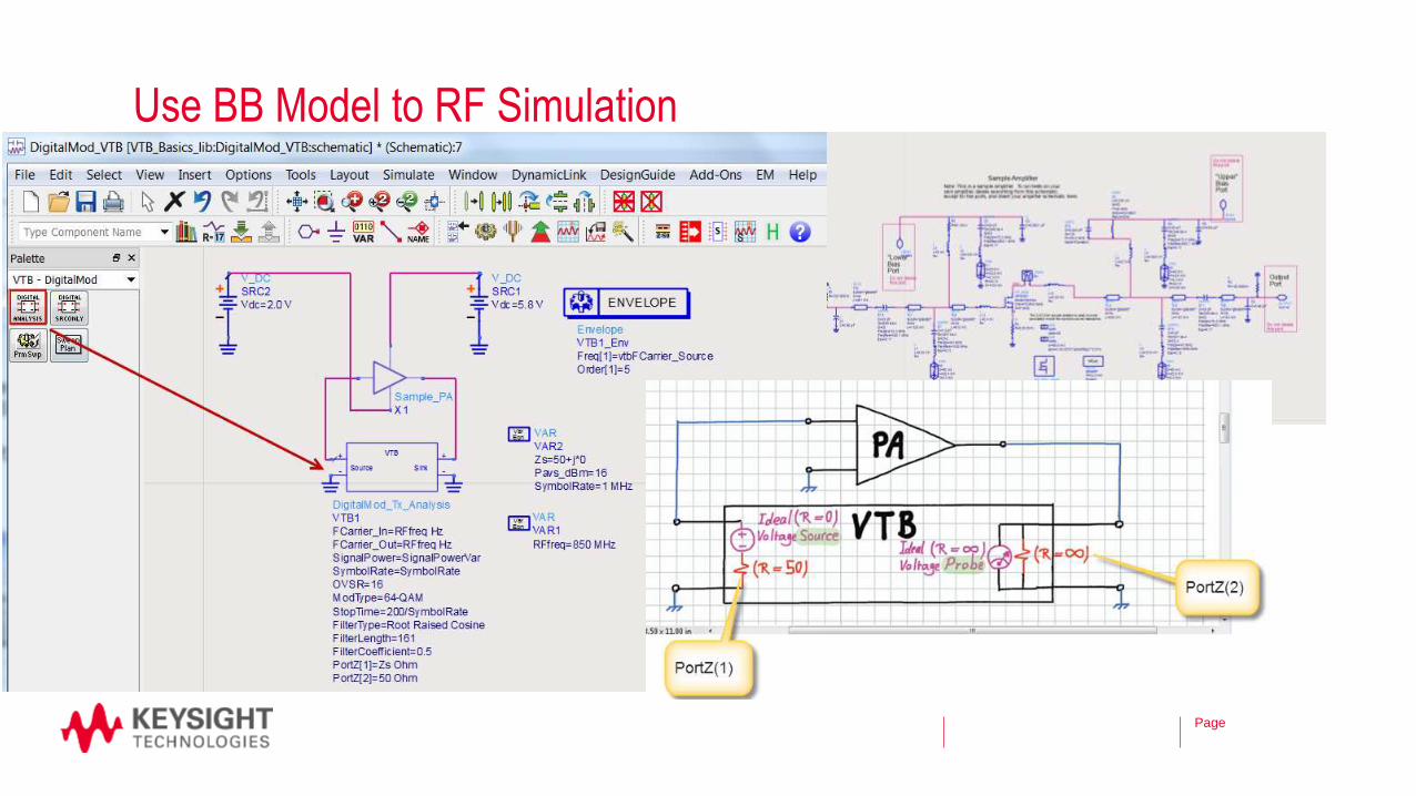
Use BB Model to RF Simulation
EEsof EDA SystemVue ©Keysight
Technologies
7

Page
Where Cross-Domain Simulation Approach Need for 5G?
EEsof EDA SystemVue
©Keysight Technologies
8

Page
Full Duplex Communication Radio
EEsof EDA SystemVue
©Keysight Technologies
9
f2
Backhaul on radio
access frequencies
Point-to-Point links
or WiFi STA 2
f1 f2
Interference
Self Interference
BTS
STA 1
Small Cell
– The devices transmit and
receive signals
simultaneously at the
same frequency
– The new breakthrough in
wireless communications
– Theoretically double the
spectral efficiency
– Self interference
cancellation need to be
addressed at both
baseband and RF domain

Page
Different Tools Used in Different Domains
EEsof EDA SystemVue
©Keysight Technologies
10
– Electro magnetic simulation
– RF circuit simulation
– Baseband algorithm verification
– System level simulation and performance evaluation
Hybrid transformer
* Full duplex transceiver chain example (image from : DUPLO project # 316369, doc: D2.1)
Electrical balance
Dual polarized antenna
Variable delay and gain Adaptive algorithms
Reference PHY IPs
• WIFI, LTE/A, Future 5G

Page
Full Duplex Transceiver Modelling
EEsof EDA SystemVue
©Keysight Technologies
11
Required Block Set
A to D D_I
A_out
D_Q
EnableExtJitter=NO
NyquistZone=1
CenterFreq=0 Hz
UserDigitalFormat=Twos-complement
UserInputSpan=2 V
UserCommonModeOffset=0 V
UserMaxSR=1e12 Hz
UserMinSR=0 Hz
UserNBits=8
UserModel=
ModelDirType=Default
Model=User specified model
A1 {AtoD_ADI@Data Flow Models}
D to A
HarmonicDistortion=None
DNL=0.0
INL=0.0
RJrms=0.0 s
RepeatOutput=1
InputDigitalFormat=Twos-complement
VRef=1.0 V
NBits=8
D1 {DtoA@Data Flow Models}
Fc
CxEnv
E1 {EnvToCx@Data Flow Models}
Amplifier
RefR=50 Ω
GCType=none
NoiseFigure=0
Gain=1
GainUnit=voltage
A2 {Amplifier@Data Flow Models}
ShowAdvancedParams=NO
RefR=50 Ω
NDensity=0 W
RefClock=
PN_Type=Random PN
PhaseNoiseData=
RandomPhase=NO
Phase=0.0 °
Power=.010 W
Frequency=1000000 Hz
O1 {Oscillator@Data Flow Models}
MATLAB_Script
M1 {MATLAB_Script@Data Flow Models}
Env
OutputFc=Center
A3 {AddEnv@Data Flow Models}
TEST
REF
BitsPerFrame=100
StartStopOption=Auto
B1 {BER_FER@Data Flow Models}
Link Adaptation & HARQ Keysight EEsof EDA
November 14, 2014
Page
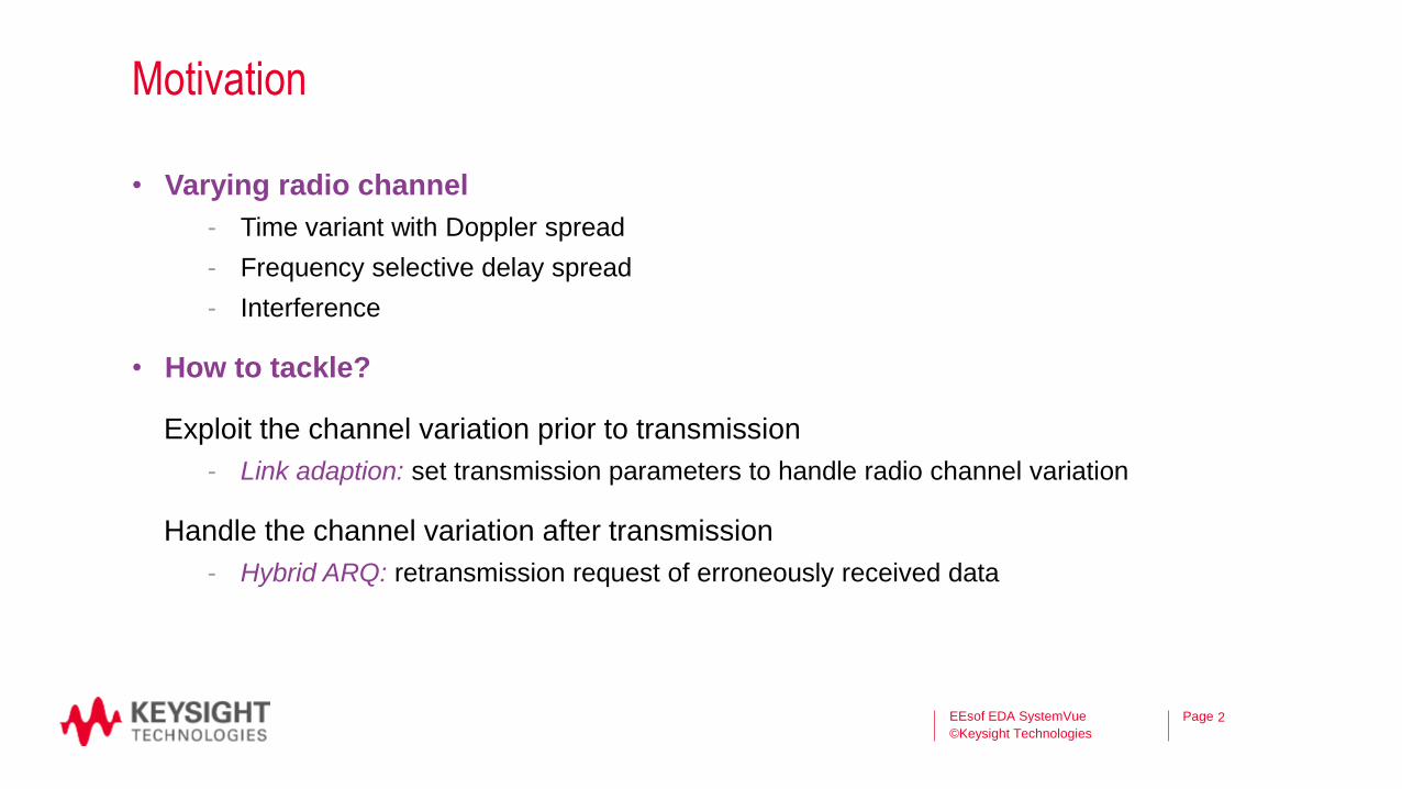
Motivation
• Varying radio channel
- Time variant with Doppler spread
- Frequency selective delay spread
- Interference
• How to tackle?
Exploit the channel variation prior to transmission
- Link adaption: set transmission parameters to handle radio channel variation
Handle the channel variation after transmission
- Hybrid ARQ: retransmission request of erroneously received data
EEsof EDA SystemVue
©Keysight Technologies
2
Page
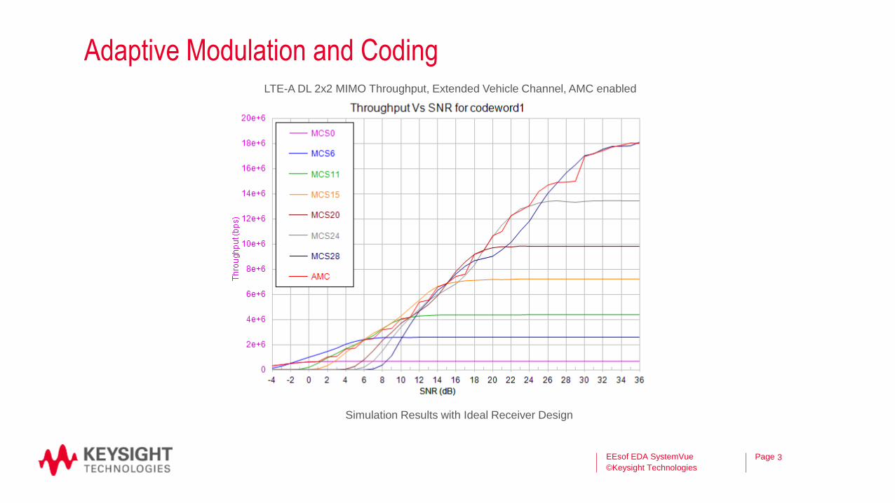
Adaptive Modulation and Coding
EEsof EDA SystemVue
©Keysight Technologies
3
LTE-A DL 2x2 MIMO Throughput, Extended Vehicle Channel, AMC enabled
Simulation Results with Ideal Receiver Design

Page
Measurement Based Throughput Evaluation
EEsof EDA SystemVue
©Keysight Technologies
4
Page
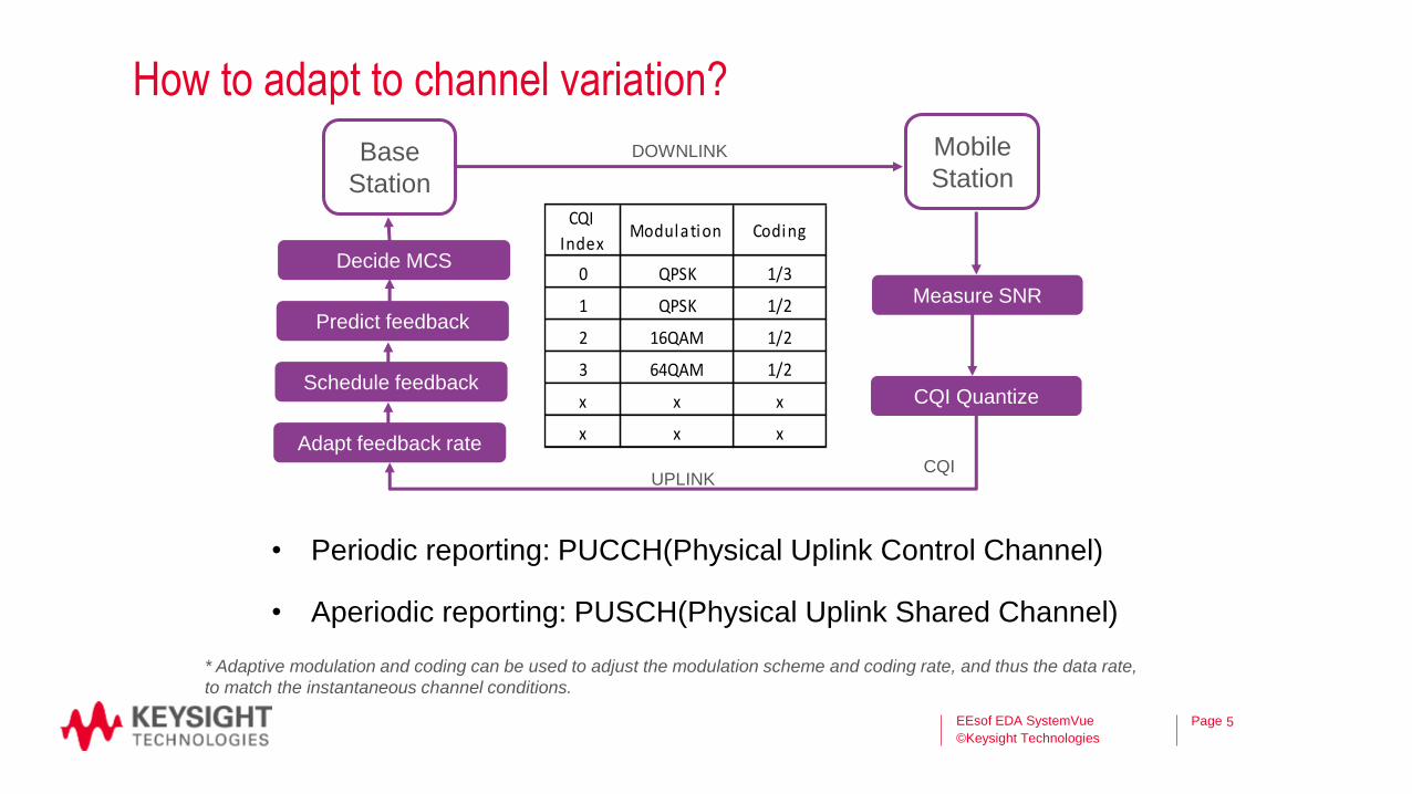
How to adapt to channel variation?
EEsof EDA SystemVue
©Keysight Technologies
5
• Periodic reporting: PUCCH(Physical Uplink Control Channel)
• Aperiodic reporting: PUSCH(Physical Uplink Shared Channel)
CQI
IndexModulation Coding
0 QPSK 1/3
1 QPSK 1/2
2 16QAM 1/2
3 64QAM 1/2
x x x
x x x
* Adaptive modulation and coding can be used to adjust the modulation scheme and coding rate, and thus the data rate,
to match the instantaneous channel conditions.
Decide MCS
Predict feedback
Schedule feedback
Adapt feedback rate
CQI Quantize
DOWNLINK
UPLINK CQI
Measure SNR
Base
Station
Mobile
Station

Page
What affect CQI Reporting Level?
EEsof EDA SystemVue
©Keysight Technologies
6
• Channel, noise and interference level
• Performance of receiver (e.g. noise figure of analog front end, performance of the
DSP modules)

Page
Model Based Simulation
EEsof EDA SystemVue
©Keysight Technologies
7
ModOUT
QUAD
OUT
Freq
Phase
Q
I
Amp
FCarrier=2e+9Hz [FCarrier]
InputType=I/QM1
SampleRate=7.68e+6Hz [SamplingRate]
Power=1W
Frequency=2e+9Hz [FCarrier]
O2
Re
Im
C1
ModOUT
QUAD
OUT
Freq
Phase
Q
I
Amp
FCarrier=2e+9Hz [FCarrier]
InputType=I/Q
M3
DeModI
Amp
Freq
Phase
Q
FCarrier=2e+9Hz [FCarrier]
OutputType=I/Q
D2
DeModI
Amp
Freq
Phase
Q
FCarrier=2e+9Hz [FCarrier]
OutputType=I/QD1
NoiseDensity
NDensity=2.108e-12W [NDensity]
NDensityType=Constant noise density
A1
Re
Im
R2
Re
Im
R1
NoiseDensity
NDensity=2.108e-12W [NDensity]
NDensityType=Constant noise densityA2
Re
Im
C2
MIMOChannel
Velocity=2.7 [Velocity]
ModelType=Extended_Vehicular_A
CorrelationType=Low [CorrelationType]
AntennaConfig=TR_2x2L1
Frame
UE1_RawBits
UE1_ChannelBits
UE1_M odSymbols
UE2_M odSymbols
UE3_M odSymbols
UE4_M odSymbols
UE5_M odSymbols
UE6_M odSymbols
PDCCH_M odSymbols
PHICH_M odSymbols
PCFICH_M odSymbols
PBCH_M odSymbols
SSS_M odSymbols
PSS_M odSymbols
DataOutUE1_HARQ_BitsUE1_TBS
UE1_PMIUE1_CQI
LTE_A
DL
Baseband
Receiver
UE1_CQIToMCS=(1x16) [0,0,0,2,4,6,8,11,1…
UE1_SNRToCQI=(1x15) [-4,-0.4,1.4,3.8,5.…
UE1_SNRFilterAlpha=0.01
UE1_SNREstimatorMode=Ideal
UE1_AMC_Delay=4 [UE1_AMC_Delay]
UE1_AMC_Enable=YESUE1_RB_Alloc=(1x2) [0,25] [UE1_RB_Alloc]
LTE_A_DL_Rcv_1
1 1 0 1 0
DataPattern=PN9
B1 {DataPattern@Data Flow Models}
1 1 0 1 0
DataPattern=PN9
B2 {DataPattern@Data Flow Models}
UE1_Data
CQI_Bits
frm _TD
frm _FD
UE1_M odSymbols
UE1_ChannelBits
SC_Status
HARQ_Bits
LTE_A
DL
Src
CSIRS_Enable=NO
UE1_CQIToMCS=(1x16) [0,0,0,2,4,6,8,11,1…
UE1_AMC_Delay=4 [UE1_AMC_Delay]
UE1_AMC_Enable=YES [UE1_AMC_Enable]
UEs_TransMode=(1x6) [2,1,1,1,1,1]
LTE_A_DL_Src_1 {LTE_A_DL_Src@LTE Advanced Models}
Fading
channel
Implement dynamic feedback mechanism for
• Hybrid ARQ
• CQI
• Transport block size information
Define link level system parameters
• FDD/TDD
• Transmission Mode
• Bandwidth etc…
Map CQI to MCS LTE
ThroughputCRC
TBS
StatusUpdatePeriod=10
SubframeStop=2000 [NumSimSubframes]
SubframeStart=10
L2 {LTE_Throughput@LTE 8.9 Models}
Throughput measurement
Page
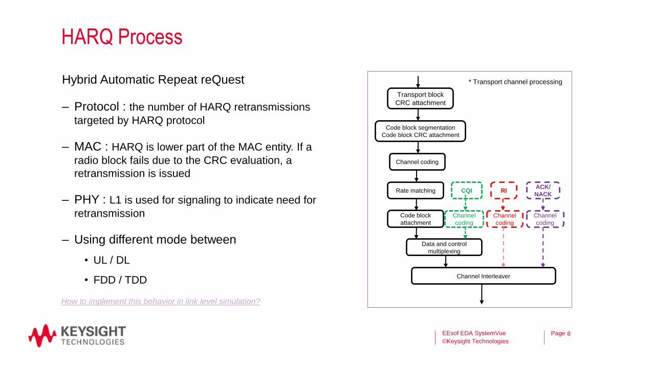
HARQ Process
EEsof EDA SystemVue
©Keysight Technologies
8
Hybrid Automatic Repeat reQuest
– Protocol : the number of HARQ retransmissions
targeted by HARQ protocol
– MAC : HARQ is lower part of the MAC entity. If a
radio block fails due to the CRC evaluation, a
retransmission is issued
– PHY : L1 is used for signaling to indicate need for
retransmission
– Using different mode between
• UL / DL
• FDD / TDD
Transport block
CRC attachment
Code block segmentation
Code block CRC attachment
Channel coding
Rate matching
Code block
attachment
Data and control
multiplexing
Channel
coding
CQI
Channel Interleaver
Channel
coding
RI
Channel
coding
ACK/
NACK
* Transport channel processing
How to implement this behavior in link level simulation?

Page
HARQ Modeling Example
EEsof EDA SystemVue
©Keysight Technologies
9
LTE_A_DL_ChannelCoder
LTE
CodeBlkSeg
CodeBlockSegmentation
LTE
CRCENCODER
CRC_Length=CRC_24A
L2
[ ]D ynamic
# rows # cols
Format=ColumnMajor
D1
TBS
LTE
TurboECODER
L3
MATCH
Rate
LTE
DataIn
ProcNum
RSN
TBS
Qm
NIR
NL
G
DataOut
LinkDir=DL
RV_Sequence=(1x4) [0,1,2,3]
MaxHARQTrans=4 [MaxHARQTrans]
NumHARQ=8 [NumHARQ]
L4
Bus=NO
Data Type=Integer Matrix
Direction=Output
PORT=2
DataOut
Bus=NO
Data Type=Integer
Direction=Output
PORT=3
Qm
Optional=YES
Bus=NO
Data Type=Integer
Direction=Input
PORT=4
HARQ_Bits
Bus=NO
Data Type=Integer
Direction=Input
PORT=1
DataIn
M2
LOGIC
NOT
Logic=NOT
L1
LimiterType=linear
Top=1
Bottom=0
K=1
L5
LTE
SCRAMBLER
PDSCH_MCH=PDSCH
q=0 [q]
n_RNTI=0 [n_RNTI]
CellID_Group=0 [CellID_Group]
CellID_Sector=0 [CellID_Sector]
LinkDir=DL
Scrambler
Optional=YES
Bus=NO
Data Type=Integer
Direction=Input
PORT=5
CQI_Bits
Controller
LTE_A
HARQ
HARQ_Bits
ProcNum
RSN
TBS
Qm
Msymb
NIR
NL
G
CQI_Bits
DMRS_NumAntPorts=1 [DMRS_NumAntPorts]
UE_TransMode=TM 1:Single Ant Port(por…
HARQ_Controller
Page
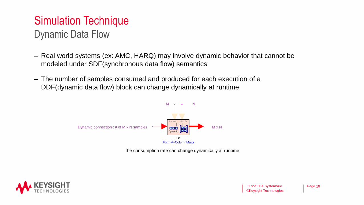
Simulation Technique
– Real world systems (ex: AMC, HARQ) may involve dynamic behavior that cannot be
modeled under SDF(synchronous data flow) semantics
– The number of samples consumed and produced for each execution of a
DDF(dynamic data flow) block can change dynamically at runtime
EEsof EDA SystemVue
©Keysight Technologies
10
Dynamic Data Flow
[ ]Dynamic
# rows # cols
Format=ColumnMajor
D1
the consumption rate can change dynamically at runtime
Dynamic connection : # of M x N samples M x N
N M

Page
Demo & Discussion
– Use LTE-A_DL_AMC example
– Review Transmitter and Receiver Blocks
– Review fading channel model parameters
– Review throughput simulation result using graph
– Show HARQ process
– Discuss about dynamic data flow
EEsof EDA SystemVue
©Keysight Technologies
11

Carrier Aggregation and Dual Band DPD
Keysight EEsof EDA
November 14, 2014
Page
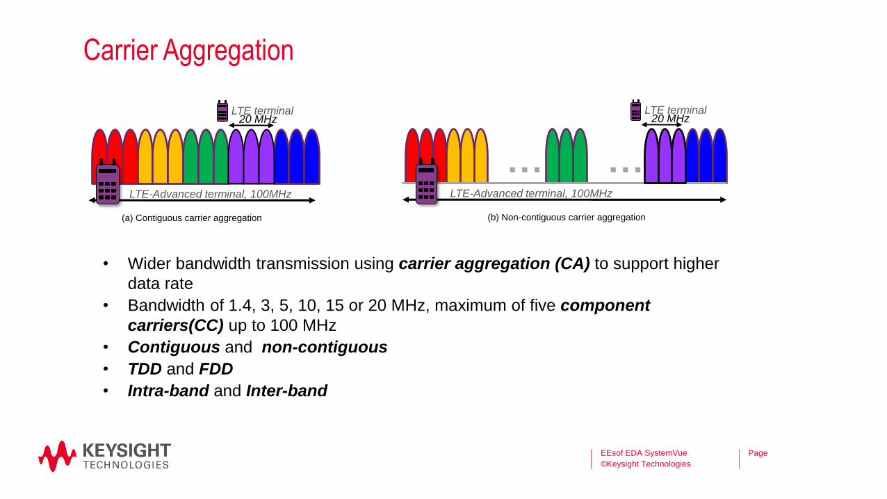
Carrier Aggregation
• Wider bandwidth transmission using carrier aggregation (CA) to support higher
data rate
• Bandwidth of 1.4, 3, 5, 10, 15 or 20 MHz, maximum of five component
carriers(CC) up to 100 MHz
• Contiguous and non-contiguous
• TDD and FDD
• Intra-band and Inter-band
20 MHz LTE terminal
LTE-Advanced terminal, 100MHz
(a) Contiguous carrier aggregation
… …
(b) Non-contiguous carrier aggregation
20 MHz LTE terminal
LTE-Advanced terminal, 100MHz
EEsof EDA SystemVue
©Keysight Technologies

Page
MAC and Physical Layer for CA
EEsof EDA SystemVue
©Keysight Technologies
MUX UE1 MUX UE2
HARQ
TB
SCHEDULING MAC
PHY
Scheduling of data
on multiple CCs
HARQ per CC
PDCCH, HARQ
ACK/NACK & CSI
for multiple CC
HARQ HARQ
TB2 TB1
UE1, R10 UE2, R8
PCC SCC
There will be 1 TB per CC unless spatial multiplexing is used
Logical Channel
Transport Channel

Page
CA Modeling for Link Level Simulation
EEsof EDA SystemVue
©Keysight Technologies
BER
CC2 @ LTE-A PHY LTE-A BB Receiver @ CC1
CC1 @ LTE-A PHY LTE-A BB Receiver @ CC1
Re
Im
R2 {Rec tToCx @Data Flow M odels }
Re
Im
R1 {Rec tToCx @Data Flow M odels }
A
Bloc k Siz es =(1x 2) [1 ,1] [[1 ,1]]
A3 {As y nc Com m utator@Data Flow M odels}
[ ] Dynam ic
# r ows # cols
Form at=Colum nM ajor
D2 {Dy nam ic Unpac k _M @Data Flow M odels}
1 1 0 1 0
DataPattern=PN9
B6 {DataPattern@Data Flow M odels}
OutputTim ing=EqualToInput
N=90000 [10*CC1_UE1_Pay load+10*CC2_UE1_Pay load]
D4 {Delay @Data Flow M odels}
DeModI
Am p
Fr eq
Phase
Q
FCarrier=2.594e+9 Hz [FCarrier1]
OutputTy pe=I/Q
D1
DeModI
Am p
Fr eq
Phase
Q
FCarrier=2.606e+9 Hz [FCarrier2]
OutputTy pe=I/Q
D3
SignalCom biner
out put
com bined
OutputSam pleRate=61.44e+6
OutputSam pleRateOption=Us er Defined
OutputFc =2.606e+9 [FCarrier2]
Bandwidth=61.44e+6 [Sam pl ingRate]
Fc =2.606e+9 [FCarrier2]
Sam pleRate=61.44e+6 [Sam pl ingRate]
S2 {SignalCom biner@Data Flow M odels}
FcChange
Bandwidth=0 Hz
OutputFc =2.594e+9 Hz [FCarrier1]
E2 {Env Fc Change@Data Flow M odels}
FcChange
Bandwidth=0 Hz
OutputFc =2.606e+9 Hz [FCarrier2]
E1 {Env Fc Change@Data Flow M odels}
M ax im um Order=1000
StopRipple=80
StopBandwidth=10e+6 Hz [CC2_BW]
Pas s Ripple=0.1
Pas s Bandwidth=9e+6 Hz [CC2_Trans BW]
FCenter=2.606e+9 Hz [FCarrier2]
F1 {BPF_Park s M c Cle l lan@Data Flow M odels}
SignalCom biner
out put
com bined
OutputSam pleRate=61.44e+6
OutputSam pleRateOption=Us er Defined
OutputFc =2.594e+9 [FCarrier1]
Bandwidth=61.44e+6 [Sam pl ingRate]
Fc =2.594e+9 [FCarrier1]
Sam pleRate=61.44e+6 [Sam pl ingRate]
S3 {SignalCom biner@Data Flow M odels}
M ax im um Order=1000
StopRipple=80
StopBandwidth=10e+6 Hz [CC1_BW]
Pas s Ripple=0.1
Pas s Bandwidth=9e+6 Hz [CC1_Trans BW]
FCenter=2.594e+9 Hz [FCarrier1]
F2 {BPF_Park s M c Cle l lan@Data Flow M odels}
Fr ame
UE1_RawBits
UE1_ChannelBits
UE1_M odSym bols
UE2_M odSym bols
UE3_M odSym bols
UE4_M odSym bols
UE5_M odSym bols
UE6_M odSym bols
PDCCH_M odSym bols
PHI CH_M odSym bols
PCFI CH_M odSym bols
PBCH_M odSym bols
SSS_M odSym bols
PSS_M odSym bols
Dat aOutUE1_HARQ _BitsUE1_TBS
UE1_PMIUE1_CQI
LTE_A
DL
Bas eband
Rec eiver
LTE_A_DL_Rc v _1
Fr ame
UE1_RawBits
UE1_ChannelBits
UE1_M odSym bols
UE2_M odSym bols
UE3_M odSym bols
UE4_M odSym bols
UE5_M odSym bols
UE6_M odSym bols
PDCCH_M odSym bols
PHI CH_M odSym bols
PCFI CH_M odSym bols
PBCH_M odSym bols
SSS_M odSym bols
PSS_M odSym bols
Dat aOutUE1_HARQ _BitsUE1_TBS
UE1_PMIUE1_CQI
LTE_A
DL
Bas eband
Rec eiver
LTE_A_DL_Rc v _2
TEST
REF
Bi ts PerFram e=90000 [BER_Sam pleStart]
StartStopOption=Sam ples
B3 {BER_FER@Data Flow M odels }
LTE
DL_EVM
Dis abled: OPEN
CC1 {LTE_DL_EVM @LTE 8.9 M odels }
LTE
DL_EVM
Dis abled: OPEN
CC2 {LTE_DL_EVM @LTE 8.9 M odels }Noise
Density
NDens i ty =21.08e-12 W [NDens i ty]
NDens i ty Ty pe=Cons tant no is e density
A1
SignalCom biner
out put
com bined
OutputSam pleRate=61.44e+6
OutputSam pleRateOption=Us er Defined
OutputFc =2.6e+9 [FCarrier]
Bandwidth=(1x 2) [61.44e+6,61.44e+6]
Fc =(1x 2) [2 .594e+9,2.606e+9] [[FCarrier1 FCarrier2]]
Sam pleRate=(1x 2) [61.44e+6,61.44e+6]
S1 {SignalCom biner@Data Flow M odels}
Re
Im
C2
1 1 0 1 0
DataPattern=PN9
B1 {DataPattern@Data Flow M odels}
Offs et=-5000 [-CC1_UE1_Pay load]
nWri te=4000 [CC2_UE1_Pay load]
nRead=9000 [CC1_UE1_Pay load+CC2_UE1_Pay load]
C4 {Chop@Data Flow M odels }
Sam pleRate=61.44e+6 Hz [CC2_Sam pl ingRate]
Power=1 W
Frequenc y =2.606e+9 Hz [FCarrier2]
O1
ModO UT
Q UAD
O UT
Fr eq
Phase
Q
I
Am p
FCarrier=2.606e+9 Hz [FCarrier2]
InputTy pe=I/Q
M 1
UE1_Data
CQ I _Bits
f r m _TD
f r m _FD
UE1_M odSym bols
UE1_ChannelBits
SC_St atusHARQ _Bits
LTE_A
DL
Src
CSIRS_Enable=NO
UE1_AM C_Enable=NO
CC2_Src
Re
Im
C1
ModO UT
Q UAD
O UT
Fr eq
Phase
Q
I
Am p
FCarrier=2.594e+9 Hz [FCarrier1]
InputTy pe=I/Q
M 2
1 1 0 1 0
DataPattern=PN9
B2 {DataPattern@Data Flow M odels}
Sam pleRate=61.44e+6 Hz [CC1_Sam pl ingRate]
Power=1 W
Frequenc y =2.594e+9 Hz [FCarrier1]
O2
UE1_Data
CQ I _Bits
f r m _TD
f r m _FD
UE1_M odSym bols
UE1_ChannelBits
SC_St atusHARQ _Bits
LTE_A
DL
Src
CSIRS_Enable=NO
UE1_AM C_Enable=NO
CC1_Src
Offs et=0
nWri te=5000 [CC1_UE1_Pay load]
nRead=9000 [CC1_UE1_Pay load+CC2_UE1_Pay load]
C3 {Chop@Data Flow M odels }
Page
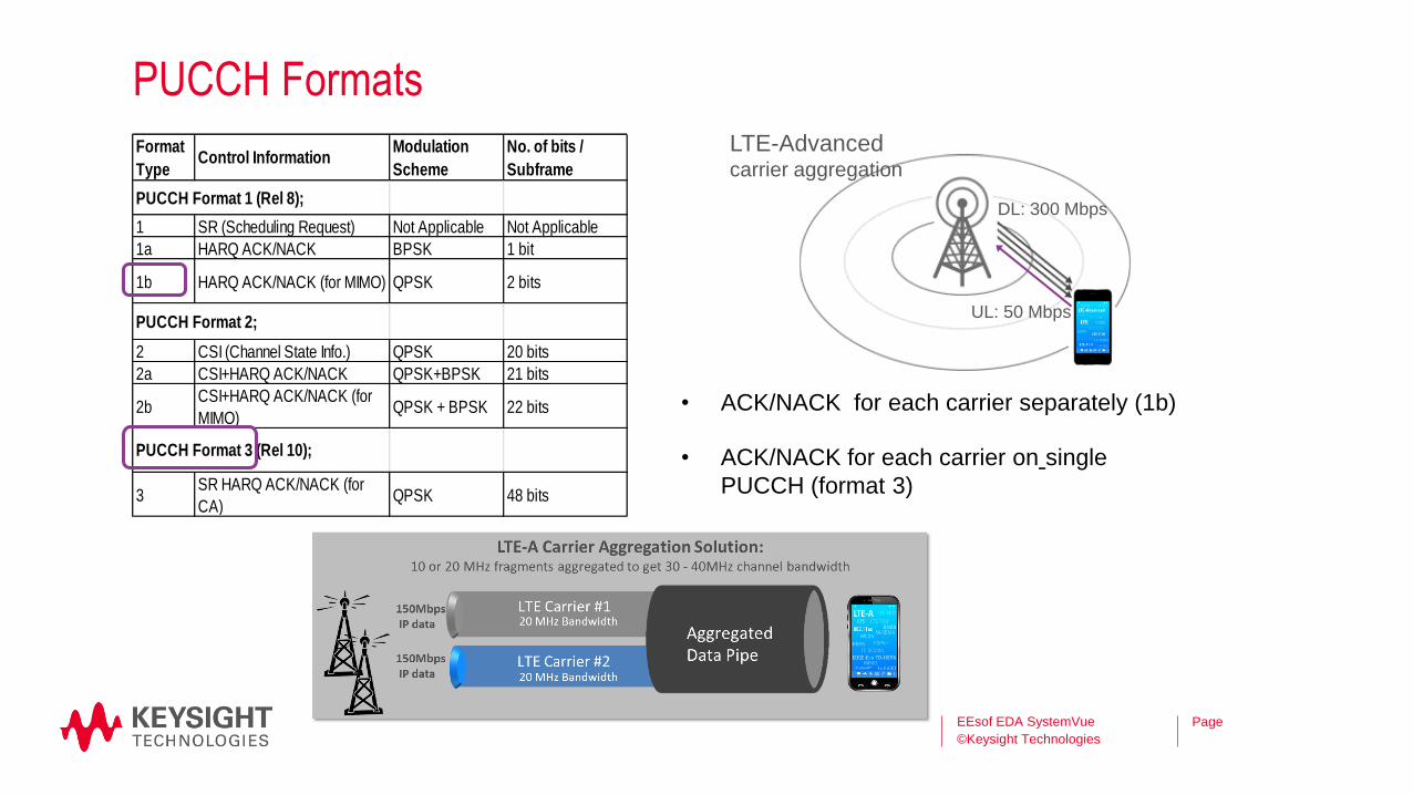
PUCCH Formats
EEsof EDA SystemVue
©Keysight Technologies
Format
TypeControl Information
Modulation
Scheme
No. of bits /
Subframe
PUCCH Format 1 (Rel 8);
1 SR (Scheduling Request) Not Applicable Not Applicable
1a HARQ ACK/NACK BPSK 1 bit
1b HARQ ACK/NACK (for MIMO) QPSK 2 bits
PUCCH Format 2;
2 CSI (Channel State Info.) QPSK 20 bits
2a CSI+HARQ ACK/NACK QPSK+BPSK 21 bits
2bCSI+HARQ ACK/NACK (for
MIMO)QPSK + BPSK 22 bits
PUCCH Format 3 (Rel 10);
3SR HARQ ACK/NACK (for
CA)QPSK 48 bits
• ACK/NACK for each carrier separately (1b)
• ACK/NACK for each carrier on single
PUCCH (format 3)
LTE-Advanced carrier aggregation
DL: 300 Mbps
UL: 50 Mbps

Page
LTE-Advanced CA signals
EEsof EDA SystemVue
©Keysight Technologies
Scenario number
Deployment scenario Transmission BWs of LTE-A carriers
# of LTE-A component carriers Bands for LTE-A
carriers Duplex modes
1 Single-band contiguous spec. alloc. @ 3.5GHz band for FDD
UL: 40 MHz
DL: 80 MHz
UL: Contiguous 2x20 MHz CCs DL: Contiguous 4x20 MHz CCs
3.5 GHz band FDD
2 Single-band contiguous spec. alloc. @ Band 40 for TDD
100 MHz Contiguous 5x20 MHz CCs Band 40 (2.3 GHz)
TDD
4
Single-band, non-contiguous spec. alloc. @ 3.5GHz band for FDD
UL: 40 MHz
DL: 80 MHz
UL: Non-contiguous 1x20 + 1x20 MHz CCs DL: Non-contiguous 2x20 + 2x20 MHz CCs
3.5 GHz band FDD
Re
Im
Env
1 1 0 1 0
1 1 0 1 0
UE1_Dat a
HARQ _Bit s
f r m _TD
f r m _FD
UE1_M odSym bols
UE1_ChannelBit s
SC_St at usUE1_PM I
LTE_A
DL
Src
UEs_n_SCID=0;0;0;0;0;0 [[0, 0, 0, 0, 0, 0]]
UserDefinedAntMappingMatrix=NO
LTE_A_DL_Src_2
FcChange
Spect rum Anal yzer
CCDF
Stop=10ms
Start=0s
CCDF_CA
CCDF
Stop=10ms
Start=0s
WoCA
ModOUT
QUAD
OUT
Freq
Phas e
Q
I
Am p
Re
Im1 1 0 1 0
1 1 0 1 0
UE1_Dat a
HARQ _Bit s
f r m _TD
f r m _FD
UE1_M odSym bols
UE1_ChannelBit s
SC_St at us
UE1_PM I
LTE_A
DL
Src
UEs_n_SCID=0;0;0;0;0;0 [[0, 0, 0, 0, 0, 0]]
UserDefinedAntMappingMatrix=NO
LTE_A_DL_Src_4
ModOUT
QUAD
OUT
Freq
Phas e
Q
I
Am p
Re
Im
1 1 0 1 0
1 1 0 1 0
UE1_Dat a
HARQ _Bit s
f r m _TD
f r m _FD
UE1_M odSym bols
UE1_ChannelBit s
SC_St at usUE1_PM I
LTE_A
DL
Src
UEs_n_SCID=0;0;0;0;0;0 [[0, 0, 0, 0, 0, 0]]
UserDefinedAntMappingMatrix=NO
LTE_A_DL_Src_3
ModOUT
QUAD
OUT
Freq
Phas e
Q
I
Am p
Re
Im
ModOUT
QUAD
OUT
Freq
Phas e
Q
I
Am p
1 1 0 1 0
1 1 0 1 0
UE1_Dat a
HARQ _Bit s
f r m _TD
f r m _FD
UE1_M odSym bols
UE1_ChannelBit s
SC_St at us
UE1_PM I
LTE_A
DL
Src
UEs_n_SCID=0;0;0;0;0;0 [[0, 0, 0, 0, 0, 0]]
UserDefinedAntMappingMatrix=NO
LTE_A_DL_Src_1
20 MHz
CCs 80 MHz
total

Page
FDD and TDD LTE-Advanced Carrier Aggregation
EEsof EDA SystemVue
©Keysight Technologies
Scenario Link Configuration PAPR of single CC,
before aggregation
PAPR with CCs,
after aggregation
Scenario 1 FDD DL 4x20 MHz CCs 8.45 dB 9.98 dB
Scenario 2 TDD DL 5x20 MHz CCs 9.17 dB 11.71 dB
Scenario 4
FDD DL 2x20+2x20MHz 8.38 dB 9.58 dB
FDD UL 20 + 20MHz 5.79 dB 6.86 dB
Scenario 1 FDD DL
Scenario 2
TDD DL
Scenario 4 FDD DL Scenario 4 FDD UL

Page
Intra-Band Carrier Aggregation
EEsof EDA SystemVue
©Keysight Technologies
–Multiple CCs are used inside of a single frequency Band (3GPP
defined bands)
–CCs can be contiguous or non-contiguous or both if more than 2 are
used
–Some chipsets support this mode with a single receiver
Page
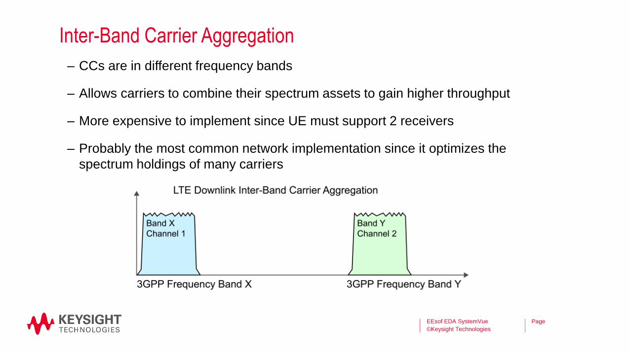
Inter-Band Carrier Aggregation
EEsof EDA SystemVue
©Keysight Technologies
– CCs are in different frequency bands
– Allows carriers to combine their spectrum assets to gain higher throughput
– More expensive to implement since UE must support 2 receivers
– Probably the most common network implementation since it optimizes the
spectrum holdings of many carriers

Page
Digital Pre-Distortion
EEsof EDA SystemVue
©Keysight Technologies
LINEAR
INPUT
POWER
OUTPUT
POWER
DPD pre-expanded peaks
INPUT
POWER
PA compresses peaks LINEAR
Baseband
Digital Pre-Distortion
RF
Power Amplification

Page
What does a DPD look like? (Volterra Model)
EEsof EDA SystemVue
©Keysight Technologies
K
k
k nznz1
)()(
Q
m
Q
m
k
l
lkkk
k
mnymmhnz0 0 1
1
1
)(),,()(
Q
m
Q
m
Q
m
mnymnymmhmnymhhnz0 0
21212
0
1110
1 21
)()(),()()()(
Volterra series pre-distorter can be described by
where
Which is a 2-dimensional summation of power series & past time envelope responses
A full Volterra produces a huge computational load.
People usually simplify it into
• Wiener model
• Hammerstein model
• Wiener-Hammerstein model
• Memory polynomial model
Page
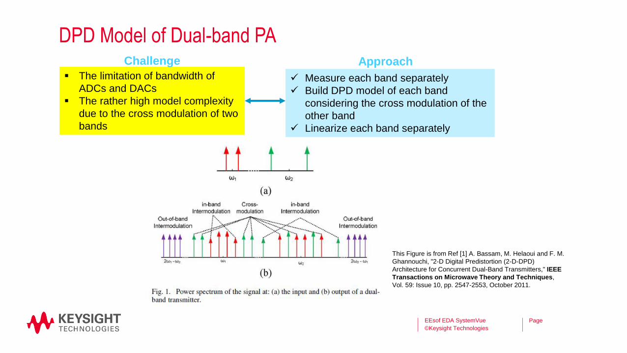
DPD Model of Dual-band PA
EEsof EDA SystemVue
©Keysight Technologies
This Figure is from Ref [1] A. Bassam, M. Helaoui and F. M.
Ghannouchi, "2-D Digital Predistortion (2-D-DPD)
Architecture for Concurrent Dual-Band Transmitters," IEEE
Transactions on Microwave Theory and Techniques,
Vol. 59: Issue 10, pp. 2547-2553, October 2011.
The limitation of bandwidth of
ADCs and DACs
The rather high model complexity
due to the cross modulation of two
bands
Measure each band separately
Build DPD model of each band
considering the cross modulation of the
other band
Linearize each band separately
Challenge Approach

Page
Dual Band DPD for Inter-Band CA
EEsof EDA SystemVue
©Keysight Technologies
Attenuator
89600
VSA
M9381A PXI VSG and M9393A PXI VSA
RF1
RF DUT
MEASUREMENT-BASED DPD
RF2
Combiner
Download Waveform
Band X Band Y

3D Wireless Channel
Keysight EEsof EDA
November 14, 2014
Page
Motivation
– Multiple-antenna (MIMO) technology is becoming mature for wireless communications
– The many antennas for better performance; data rate and link reliability
– Challenged by increased complexity of the hardware and energy consumption
– More signal processing challenges needs to be addressed thru simulation in early
design phase
EEsof EDA SystemVue
©Keysight Technologies
2
Page
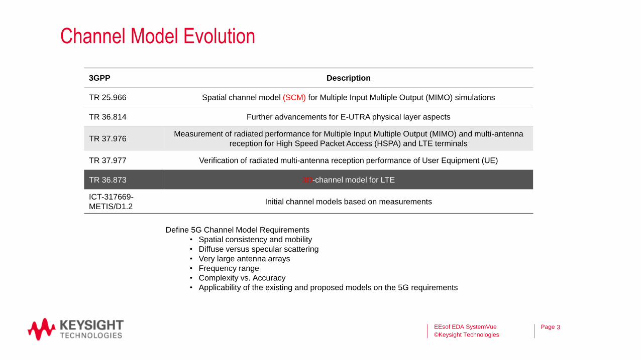
Channel Model Evolution
EEsof EDA SystemVue
©Keysight Technologies
3
3GPP Description
TR 25.966 Spatial channel model (SCM) for Multiple Input Multiple Output (MIMO) simulations
TR 36.814 Further advancements for E-UTRA physical layer aspects
TR 37.976 Measurement of radiated performance for Multiple Input Multiple Output (MIMO) and multi-antenna
reception for High Speed Packet Access (HSPA) and LTE terminals
TR 37.977 Verification of radiated multi-antenna reception performance of User Equipment (UE)
TR 36.873 3D-channel model for LTE
ICT-317669-
METIS/D1.2 Initial channel models based on measurements
Define 5G Channel Model Requirements
• Spatial consistency and mobility
• Diffuse versus specular scattering
• Very large antenna arrays
• Frequency range
• Complexity vs. Accuracy
• Applicability of the existing and proposed models on the 5G requirements
Page
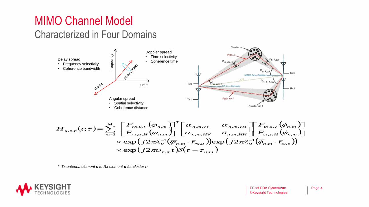
MIMO Channel Model
EEsof EDA SystemVue
©Keysight Technologies
4
Characterized in Four Domains
time
frequency
Delay spread
• Frequency selectivity
• Coherence bandwidth
Doppler spread
• Time selectivity
• Coherence time
Angular spread
• Spatial selectivity
• Coherence distance
mnmn
stxmnurxmn
mnHstx
mnVstx
HHmnHVmn
VHmnVVmn
T
mnHurx
mnVurxM
m
nsu
tj
rjrj
F
F
aF
FtH
,,
,,
1
0,,
1
0
,,,
,,,
,,,,
,,,,
,,,
,,,
1
,,
2exp
2exp2exp
;
* Tx antenna element s to Rx element u for cluster n

Page
Coordinate Systems
EEsof EDA SystemVue
©Keysight Technologies
5
AoD
ZoD
LCS AoA
ZoA
LCS
GCS
GCS : Global Coordinate System
LCS : Local Coordinate System
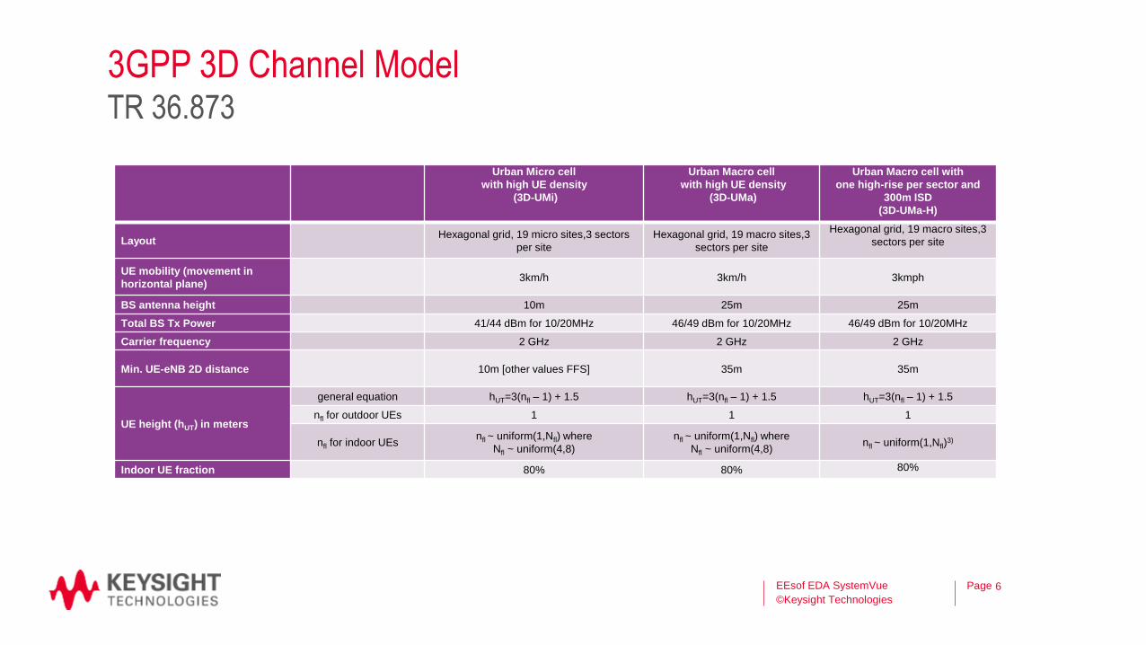
Page
3GPP 3D Channel Model
EEsof EDA SystemVue
©Keysight Technologies
6
TR 36.873
Urban Micro cell
with high UE density
(3D-UMi)
Urban Macro cell
with high UE density
(3D-UMa)
Urban Macro cell with
one high-rise per sector and
300m ISD
(3D-UMa-H)
Layout Hexagonal grid, 19 micro sites,3 sectors
per site
Hexagonal grid, 19 macro sites,3
sectors per site
Hexagonal grid, 19 macro sites,3
sectors per site
UE mobility (movement in
horizontal plane) 3km/h 3km/h 3kmph
BS antenna height 10m 25m 25m
Total BS Tx Power 41/44 dBm for 10/20MHz 46/49 dBm for 10/20MHz 46/49 dBm for 10/20MHz
Carrier frequency 2 GHz 2 GHz 2 GHz
Min. UE-eNB 2D distance 10m [other values FFS] 35m 35m
UE height (hUT) in meters
general equation hUT=3(nfl – 1) + 1.5 hUT=3(nfl – 1) + 1.5 hUT=3(nfl – 1) + 1.5
nfl for outdoor UEs 1 1 1
nfl for indoor UEs nfl ~ uniform(1,Nfl) where
Nfl ~ uniform(4,8)
nfl ~ uniform(1,Nfl) where
Nfl ~ uniform(4,8) nfl ~ uniform(1,Nfl)
3)
Indoor UE fraction 80% 80% 80%

Page
Antenna Modelling Parameters
EEsof EDA SystemVue
©Keysight Technologies
7
Parameter Applicability Values
Number of horizontal antenna elements cross-pol (X) 2, 4, 8
co-pol (| |) 1, 2, 4, 8
Polarization slant angle cross-pol (X) +/- 450
co-pol (| |) 00
Horizontal antenna element spacing dH 0.5λ baseline (other values FFS)
Antenna element vertical radiation
pattern (dB)
Antenna element horizontal radiation
pattern (dB)
3D-UMa, 3D-UMi,
LPN deployments
3D-UMi, LPN deployments FFS:
Combining method for 3D antenna
element pattern (dB)
Maximum directional gain of an antenna
element GE,max 8 dBi

Page
Problems and Solutions
EEsof EDA SystemVue
©Keysight Technologies
8
Throughput
LTE-A BB Source
Tx RF
MIMOChannel
Rx RF
LTE-A BB ReceiverRe
Im
C8
ModO UT
Q UAD
O UT
Fr eq
Phase
Q
I
Am p
FCarrier=2e+9Hz [FCarrier]
InputTy pe=I/Q
M8
Re
Im
C9
ModO UT
Q UAD
O UT
Fr eq
Phase
Q
I
Am p
FCarrier=2e+9Hz [FCarrier]
InputTy pe=I/Q
M7
ModO UT
Q UAD
O UT
Fr eq
Phase
Q
I
Am p
FCarrier=2e+9Hz [FCarrier]InputTy pe=I/Q
M6
Re
Im
C7
ModO UT
Q UAD
O UT
Fr eq
Phase
Q
I
Am p
FCarrier=2e+9Hz [FCarrier]
InputTy pe=I/Q
M5
Re
Im
C6
Sam pleRate=15.36e+6Hz [Sam pl ingRate]
Power=1W
Frequenc y =2e+9Hz [FCarrier]O1
OutputTim ing=BeforeInputN=7
D11 {Delay @Data Flow M odels}
Fc
CxEnv
E5 {Env ToCx @Data Flow M odels}
Fc
CxEnv
E6 {Env ToCx @Data Flow M odels}
Fc
CxEnv
E7 {Env ToCx @Data Flow M odels}
Fc
CxEnv
E8 {Env ToCx @Data Flow M odels}
DeMod I
Am p
Fr eq
Phase
Q
FCarrier=2e+9Hz [FCarrier]OutputTy pe=I/Q
D2
Re
Im
R1 {Rec tToCx @Data Flow M odels}
Re
Im
R2 {Rec tToCx @Data Flow M odels}
DeModI
Am p
Fr eq
Phase
Q
FCarrier=2e+9Hz [FCarrier]
OutputTy pe=I/Q
D7
Re
Im
R4 {Rec tToCx @Data Flow M odels}
Fc
EnvCx
Fc =2e+9Hz [FCarrier]
C17 {Cx ToEnv @Data Flow M odels}
1 1 0 1 0
DataPattern=PN15
B4
1 1 0 1 0
DataPattern=PN9
B2
Re
Im
C5
ModO UT
Q UAD
O UT
Fr eq
Phase
Q
I
Am p
FCarrier=2e+9Hz [FCarrier]
InputTy pe=I/Q
M4
Re
Im
C4
ModO UT
Q UAD
O UT
Fr eq
Phase
Q
I
Am p
FCarrier=2e+9Hz [FCarrier]
InputTy pe=I/Q
M3
Re
Im
C3
Re
Im
C2
Fc
EnvCx
Fc =2e+9Hz [FCarrier]
C16 {Cx ToEnv @Data Flow M odels}
Fc
EnvCx
Fc =2e+9Hz [FCarrier]
C15 {Cx ToEnv @Data Flow M odels}
Fc
EnvCx
Fc =2e+9Hz [FCarrier]
C14 {Cx ToEnv @Data Flow M odels}
Fc
EnvCx
Fc =2e+9Hz [FCarrier]
C13 {Cx ToEnv @Data Flow M odels}
Fc
EnvCx
Fc =2e+9Hz [FCarrier]
C12 {Cx ToEnv @Data Flow M odels}
Fc
EnvCx
Fc =2e+9Hz [FCarrier]
C1 {Cx ToEnv @Data Flow M odels}
Fc
EnvCx
Fc =2e+9Hz [FCarrier]
C11 {Cx ToEnv @Data Flow M odels}
NoiseDensity
NDens i ty =167.5e-12W [NDensity]NDens i ty Ty pe=Cons tant no ise density
A2
NoiseDensity
NDens i ty =167.5e-12W [NDensity]
NDens i ty Ty pe=Cons tant no ise density
A1
NoiseDensity
NDens i ty =167.5e-12W [NDensity]
NDens i ty Ty pe=Cons tant no ise density
A4
NoiseDensity
NDens i ty =167.5e-12W [NDensity]
NDens i ty Ty pe=Cons tant no ise density
A3
NoiseDensity
NDens i ty =167.5e-12W [NDensity]
NDens i ty Ty pe=Cons tant no ise density
A8
NoiseDensity
NDens i ty =167.5e-12W [NDensity]
NDens i ty Ty pe=Cons tant no ise density
A7
NoiseDensity
NDens i ty =167.5e-12W [NDensity]
NDens i ty Ty pe=Cons tant no ise density
A5
NoiseDensity
NDens i ty =167.5e-12W [NDensity]
NDens i ty Ty pe=Cons tant no ise density
A6
DeMod I
Am p
Fr eq
Phase
Q
FCarrier=2e+9Hz [FCarrier]
OutputTy pe=I/Q
D6
DeModI
Am p
Fr eq
Phase
Q
FCarrier=2e+9Hz [FCarrier]
OutputTy pe=I/Q
D8
DeModI
Am p
Fr eq
Phase
Q
FCarrier=2e+9Hz [FCarrier]
OutputTy pe=I/Q
D9
DeModI
Am p
Fr eq
Phase
Q
FCarrier=2e+9Hz [FCarrier]
OutputTy pe=I/Q
D4
DeModI
Am p
Fr eq
Phase
Q
FCarrier=2e+9Hz [FCarrier]
OutputTy pe=I/Q
D5
DeModI
Am p
Fr eq
Phase
Q
FCarrier=2e+9Hz [FCarrier]
OutputTy pe=I/Q
D3
Re
Im
R3 {Rec tToCx @Data Flow M odels}
Re
Im
R8 {Rec tToCx @Data Flow M odels}
Re
Im
R7 {Rec tToCx @Data Flow M odels}
Re
Im
R5 {Rec tToCx @Data Flow M odels}
Re
Im
R6 {Rec tToCx @Data Flow M odels}
1
Value=1
C10 {Cons t@Data Flow M odels}
LTE
Thr oughputCRC
TBS
Status UpdatePeriod=1
Subfram eStop=2000 [Num Subframes]
Subfram eStart=1
L1 {LTE_Throughput@LTE 8.9 M odels}
Fc
CxEnv
E4 {Env ToCx @Data Flow M odels}
Fc
CxEnv
E3 {Env ToCx @Data Flow M odels}
Fc
CxEnv
E2 {Env ToCx @Data Flow M odels}
Fc
CxEnv
E1 {Env ToCx @Data Flow M odels}
ModO UT
Q UAD
O UT
Fr eq
Phase
Q
I
Am p
FCarrier=2e+9Hz [FCarrier]
InputTy pe=I/Q
M2
ModO UT
Q UAD
O UT
Fr eq
Phase
Q
I
Am p
FCarrier=2e+9Hz [FCarrier]
InputTy pe=I/Q
M1
UE1_Data
CQ I _Bits
f r m _TD
f r m _FD
UE1_M odSym bols
UE1_ChannelBits
SC_St atusHARQ _Bits
LTE_A
DL
Src
CSIRS_Enable=NO
UE1_AM C_Enable=NO
UEs _n_RNTI=(1x 6) [1 ,2,3,4,5,6]UEs _Spec i fic RS=(1x 6) [0 ,0,0,0,0,0]
UEs _Trans M ode=(1x 6) [8 ,1,1,1,1,1]
LTE_A_DL_Src_1
Fr ame
UE1_RawBits
UE1_ChannelBits
UE1_M odSym bols
UE2_M odSym bols
UE3_M odSym bols
UE4_M odSym bols
UE5_M odSym bols
UE6_M odSym bols
PDCCH_M odSym bols
PHI CH_M odSymbols
PCFI CH_M odSymbols
PBCH_M odSym bols
SSS_M odSym bols
PSS_M odSym bols
Dat aOutUE1_HARQ _BitsUE1_TBSUE1_PMIUE1_CQI
LTE_A
DL
Bas eband
Rec eiver
CSIRS_Enable=NO
UE1_AM C_Enable=NOUEs _Spec i fic RS=(1x 6) [1 ,0,0,0,0,0]
UEs _Trans M ode=(1x 6) [8 ,1,1,1,1,1]
LTE_A_DL_Rc v_1
LTEAdvance_Channel
Corre la tionM atrix OutputFlag=NO
ChannelCoeffic ientOutputFlag=NO
Us ePathLos s M odel=NOUs eIntraClus terDelay s=NO
Us eLOS=NO
Us eShadowM odel=NO
Us ePolaris e=NO
Us eFix edCDLParam eter=YES
DropInterv a l=0.05s
M SDirec tion=30M SVeloc i ty =5.4e-3 [M s Velocity]
ThetaM s=0
ThetaBs=0
Rx AntennaPatternTy pe=Om niDirectional
Rx Pos i tion_Y=(1x 8) [0 ,1,2,3,4,5,6,7]
Rx Pos i tion_X=(1x 8) [0 ,0,0,0,0,0,0,0]
Num berofRx=8
Tx RotationAngle=0Tx AntennaPatternTy pe=Om niDirectional
Tx Pos i tion_Y=(1x 8) [0 ,1,2,3,4,5,6,7]
Tx Pos i tion_X=(1x 8) [0 ,0,0,0,0,0,0,0]
Num berofTx=8
Seed=10
ChannelL ink Direc tion=Downlink
Sam pleRate=15.36e+6Hz [Sam pl ingRate]CarrierFrequenc y =2e+9Hz
LTEAdv anc eSc enarioTy pe=InH
L2 {LTEAdv anc e_Channel@M IM O Channel Models}
% Channel matrix
Channel = eye(8);
ChIn = zeros(8,1);
ChOut = zeros(8,1);
for i=1:8
ChIn(i) = input{i};
end
ChOut = Channel*ChIn;
% Add your script here
for i=1:8
output{i} = ChOut(i);
End

Page
Simulation Parameters Snap Shots
EEsof EDA SystemVue
©Keysight Technologies
9

Coordinated Multi-Points Keysight EEsof EDA
November 14, 2014

Page
Motivation
– CoMP is a wide range of techniques that enable dynamic coordination with
multiple geographically separated eNBs
– To enhance the overall system performance
– To utilize the resources more effectively and improve the end user service
quality
– Cell edges are the most challenging as low signal level and interference from
neighboring eNBs
EEsof EDA SystemVue
©Keysight Technologies
2

Page
Coordinated Multi-Points
EEsof EDA SystemVue
©Keysight Technologies
3
Exchange of feedback report thru backhaul
eNodeB RRE
UE1 UE2
Cell
eNodeB Cell
UE RRE
Figure. Coordinated beamforming / scheduling
Figure. Joint Processing or Dynamic cell selection
Dynamic points selection
Coherent/Non-coherent transmission
PMI/CQI/RI feedback extensions

Page
Dynamic Point Selection Simulation Example
EEsof EDA SystemVue
©Keysight Technologies
4
BER
LTE-A BB Receiver
Re
Im
R2 {RectToCx@Data Flow Models}
DeModI
Amp
FreqPhase
Q
FCarrier=2e+9Hz [FCarrier]
OutputType=I/Q
D3
NoiseDensity
NDensity=83.93e-12W [NDensity]
NDensityType=Constant noise density
A1
Re
Im
C2
ModOUT
QUADOUT
Freq
PhaseQ
IAmp
FCarrier=2e+9Hz [FCarrier]
InputType=I/Q
M1
SampleRate=15.36e+6Hz [SamplingRate]
Power=1W
Frequency=2e+9Hz [FCarrier]
O1
Re
Im
C1
SampleRate=15.36e+6Hz [SamplingRate]
Power=1W
Frequency=2e+9Hz [FCarrier]
O2
ModOUT
QUADOUT
Freq
PhaseQ
IAmp
FCarrier=2e+9Hz [FCarrier]
InputType=I/Q
M2
Env
OutputFc=Center
A2 {AddEnv@Data Flow Models}
ChannelOut
Taps
ModelType=Extended_Vehicular_A
C5
Logic=NOT
L1 {Logic@Data Flow Models}
OutputTiming=BeforeInput
N=7 [CQI_Delay-1]
D1 {Delay@Data Flow Models}
ChannelOut
Taps
ModelType=Extended_Vehicular_A
C3 {CommsChannel@Data Flow Models}
OutputTiming=BeforeInput
N=7
D2 {Delay@Data Flow Models}
UE1_Dat a
CQ I _Bit s
f r m _TD
f r m _FD
U E 1_M odSym bols
U E 1 _ChannelBit s
SC_St at us
HARQ _Bit s
LTE_A
DL
Src
LTE_A_DL_Src_1
UE1_Dat a
CQ I _Bit s
f r m _TD
f r m _FD
U E 1_M odSym bols
U E 1 _ChannelBit s
SC_St at us
HARQ _Bit s
LTE_A
DL
Src
LTE_A_DL_Src_2
Fr am e
U E 1_RawBit s
U E 1 _ChannelBit s
U E 1_M odSym bols
U E 2_M odSym bols
U E 3_M odSym bols
U E 4_M odSym bols
U E 5_M odSym bols
U E 6_M odSym bols
P D C C H_M odSym bols
P H I CH_M odSym bols
P C F I CH_M odSym bols
P B C H_M odSym bols
S S S_M odSym bols
P S S_M odSym bols
Dat aO utU E 1_HARQ _Bit sUE1_TBS
UE1_PM IUE1_CQ I
LTE_A
DL
Baseband
Receiver
LTE_A_DL_Rcv_1
1 1 0 1 0
DataPattern=PN9
B6 {DataPattern@Data Flow Models}
r ef
t est LTE_A
BER_FER
L3 {LTE_A_BER_FER@LTE Advanced Models}
LTE
ThroughputCRC
TBS
L2 {LTE_Throughput@LTE 8.9 Models}
1 1 0 1 0
DataPattern=PN9
B2 {DataPattern@Data Flow Models}
1 1 0 1 0
DataPattern=PN9
B1 {DataPattern@Data Flow Models}
CQI
Feedback
Different
Cell-ID Different
Channel
Path
Throughput
Measurement
BS1
BS2
UE1
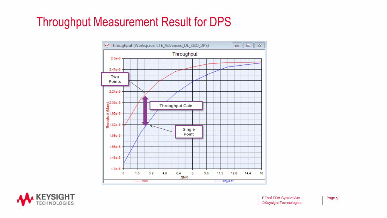
Page
Throughput Measurement Result for DPS
EEsof EDA SystemVue
©Keysight Technologies
5
Single
Point
Two
Points
Throughput Gain
Page
Signaling support for CoMP
– Release 8/9: Cell-specific RS (CRS) for up to 4 layer SM
– Release 10: Channel state information reference signal (CSI-RS) came with 8-layer
spatial multiplexing
– Release 11: Multipoint CSI feedback framework
– Release12: Enhancements to CSI from terminals to the network
– Beyond: Further extensions
EEsof EDA SystemVue
©Keysight Technologies
6
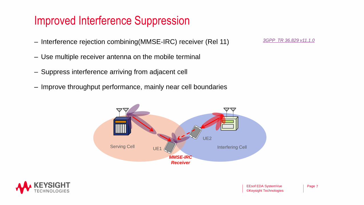
Page
Improved Interference Suppression
– Interference rejection combining(MMSE-IRC) receiver (Rel 11)
– Use multiple receiver antenna on the mobile terminal
– Suppress interference arriving from adjacent cell
– Improve throughput performance, mainly near cell boundaries
EEsof EDA SystemVue
©Keysight Technologies
7
UE1
UE2
Serving Cell Interfering Cell
MMSE-IRC
Receiver
3GPP TR 36.829 v11.1.0

Page
Algorithm Validation
EEsof EDA SystemVue
©Keysight Technologies
8
MMSE-IRC
LTE_A
DL DMRS
UE_SpecificRS=Port 7 [UEs_SpecificRS(1)]
n_SCID=0 [UE1_n_SCID]
NumOfLayers=1 [UEs_NumOfLayers(1)]
RB_Alloc=(1x2) [0,8] [UE1_RB_Alloc]
RB_AllocType=StartRB + NumRBs
RB_Gap=Ngap1 [RB_Gap]
RB_MappingType=Localized [RB_MappingType]
CellID_Group=0 [CellID_Group]
CellID_Sector=0 [CellID_Sector]
CyclicPrefix=Normal [CyclicPrefix]
Bandwidth=BW 5 MHz [Bandwidth]
FrameMode=FDD [FrameMode]
DMRS {LTE_A_DL_DMRS@LTE Advanced Models}
DMRS
input
Coef
LTE_A
DL_ChEstimator
SubframeIgnored=1 [SubframeIgnored]
Fmax=100Hz [Fmax]
Tmax=1e-6s [Tmax]
SNR=15 [SNR]
MMSE_RBWinLen=3 [MMSE_RBWinLen]
ChEstimatorMode=Linear [ChEstimatorMode]
UE_SpecificRS=Port 7 [UEs_SpecificRS(1)]
UE_TransMode=TM 8:Dual-Layer transmissi…
RB_Alloc=(1x2) [0,8] [UE1_RB_Alloc]
RB_AllocType=StartRB + NumRBs
RB_Gap=Ngap1 [RB_Gap]
RB_MappingType=Localized [RB_MappingType]
CyclicPrefix=Normal [CyclicPrefix]
NumRxAnts=Rx1 [NumRxAnts]
NumOfLayers=1 [UEs_NumOfLayers(1)]
CRS_NumAntPorts=CRS_Tx1 [CRS_NumAntPorts]
Bandwidth=BW 5 MHz [Bandwidth]
SpecialSF_Config=Config 0
TDD_Config=Config 0 [TDD_Config]
FrameMode=FDD [FrameMode]
H_DataIn
H_PSCH
H_SSCH
H_PBCH
H_PDCCH
H_PCFICH
H_PHICH
H_Data_UE6
H_Data_UE5
H_Data_UE4
H_Data_UE3
H_Data_UE2
H_Data_UE1
LTE_A_DL
MIMO
DemuxCIR
CSIRS_PowerRatio=0 [CSIRS_PowerRatio]
L1 {LTE_A_DL_MIMO_DemuxCIR@LTE Advanced Models}
MATLAB_ScriptCoef
input
DMRS
M2 {MATLAB_Script@Data Flow Models}
New
enhanced
algorithm
Legacy MMSE Algorithm
FILL
HOLES
Page
Demo & Discussion
– Use LTE-A_DL_DPS example
– Review Transmitter and Receiver Blocks
– Review fading channel model parameters
– Review throughput simulation result using graph
– Discuss why CoMP is important for 4G and 5G research
EEsof EDA SystemVue
©Keysight Technologies
9

Page
Try SystemVue
– Obtain a “FREE” 45-day evaluation copy of SystemVue and explore how SystemVue
can help with early 5G systems exploration and evaluation
• http://www.keysight.com/find/eesof-systemvue-evaluation
– Early collaboration on 5G modem architectures and systems
• Contact your Keysight sales representative
• Or, e-mail to: [email protected]
EEsof EDA SystemVue
©Keysight Technologies
1

Page
Resources
• SystemVue : www.keysight.com/find/eesof-systemvue
• 5G Library: www.keysight.com/find/eesof-systemvue-5g-exploration
- LTE & LTE-A : www.keysight.com/find/cellular or www.keysight.com/find/eesof-systemvue-lte-advanced
- MIMO Channel : www.keysight.com/find/eesof-systemvue-channel-builder
- Knowledge center: www.keysight.com/find/eesof-knowledgecenter
- Keysight EDA software: www.keysight.com/find/eesof
- Keysight EEsof EDA YouTube : www.keysight.com/find/eesof-videos
- FPGA Flow YouTube Video : http://youtu.be/8EmuV6EzcMQ
- ESL Applications Center: www.keysight.com/find/eesof-esl-applications-center
- ESL Design Notebook: www.keysight.com/find/eesof-esl-design-notebook
EEsof EDA SystemVue
©Keysight Technologies
2


