
SIV52005-3.6
© 2014 Altera Corporation. All rights reserved. ALTERA, ARRIare trademarks of Altera Corporation and registered in the U.Strademarks or service marks are the property of their respectivsemiconductor products to current specifications in accordanceservices at any time without notice. Altera assumes no responsdescribed herein except as expressly agreed to in writing by Alon any published information and before placing orders for pr
Stratix IV Device HandbookVolume 2: TransceiversJanuary 2014
January 2014SIV52005-3.6
5. Dynamic Reconfiguration in Stratix IVDevices
Stratix® IV GX and GT transceivers allow you to dynamically reconfigure different portions of the transceivers without powering down any part of the device. This chapter describes and provides examples about the different modes available for dynamic reconfiguration.
You can use the ALTGX_RECONFIG instance to reconfigure the physical medium attachment (PMA) controls, functional blocks, clock multiplier unit (CMU) phase-locked loops (PLLs), receiver clock data recovery (CDR), and input reference clocks of a transceiver channel.
Additionally, you can monitor the receiver eye width, implement decision feedback control, and achieve adaptive equalization (AEQ) control with dynamic reconfiguration.
This chapter contains the following sections:
■ “Glossary of Terms” on page 5–1
■ “Dynamic Reconfiguration Controller Architecture” on page 5–3
■ “Quartus II MegaWizard Plug-In Manager Interfaces to Support Dynamic Reconfiguration” on page 5–4
■ “Dynamic Reconfiguration Modes Implementation” on page 5–12
■ “Dynamic Reconfiguration Controller Port List” on page 5–78
■ “Error Indication During Dynamic Reconfiguration” on page 5–90
■ “Dynamic Reconfiguration Duration” on page 5–91
■ “Dynamic Reconfiguration (ALTGX_RECONFIG Instance) Resource Utilization” on page 5–94
■ “Functional Simulation of the Dynamic Reconfiguration Process” on page 5–95
■ “Dynamic Reconfiguration Examples” on page 5–96
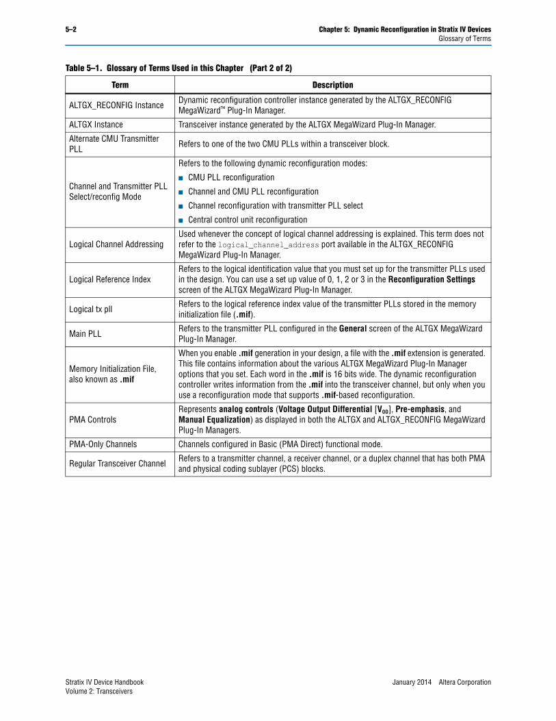
Glossary of TermsTable 5–1 lists the terms used in this chapter:
Table 5–1. Glossary of Terms Used in this Chapter (Part 1 of 2)
Term Description
AEQ Control Logic AEQ control logic is soft IP that you can enable in the dynamic reconfiguration controller.
AEQ Hardware AEQ hardware is circuitry that you can enable in the receiver portion of the transceivers.
A, CYCLONE, HARDCOPY, MAX, MEGACORE, NIOS, QUARTUS and STRATIX words and logos . Patent and Trademark Office and in other countries. All other words and logos identified as e holders as described at www.altera.com/common/legal.html. Altera warrants performance of its with Altera's standard warranty, but reserves the right to make changes to any products and ibility or liability arising out of the application or use of any information, product, or service tera. Altera customers are advised to obtain the latest version of device specifications before relying oducts or services.
Feedback Subscribe
ISO 9001:2008 Registered
5–2 Chapter 5: Dynamic Reconfiguration in Stratix IV DevicesGlossary of Terms
ALTGX_RECONFIG Instance Dynamic reconfiguration controller instance generated by the ALTGX_RECONFIG MegaWizard™ Plug-In Manager.
ALTGX Instance Transceiver instance generated by the ALTGX MegaWizard Plug-In Manager.
Alternate CMU Transmitter PLL Refers to one of the two CMU PLLs within a transceiver block.
Channel and Transmitter PLL Select/reconfig Mode
Refers to the following dynamic reconfiguration modes:
■ CMU PLL reconfiguration
■ Channel and CMU PLL reconfiguration
■ Channel reconfiguration with transmitter PLL select
■ Central control unit reconfiguration
Logical Channel AddressingUsed whenever the concept of logical channel addressing is explained. This term does not refer to the logical_channel_address port available in the ALTGX_RECONFIG MegaWizard Plug-In Manager.
Logical Reference IndexRefers to the logical identification value that you must set up for the transmitter PLLs used in the design. You can use a set up value of 0, 1, 2 or 3 in the Reconfiguration Settings screen of the ALTGX MegaWizard Plug-In Manager.
Logical tx pll Refers to the logical reference index value of the transmitter PLLs stored in the memory initialization file (.mif).
Main PLL Refers to the transmitter PLL configured in the General screen of the ALTGX MegaWizard Plug-In Manager.
Memory Initialization File, also known as .mif
When you enable .mif generation in your design, a file with the .mif extension is generated. This file contains information about the various ALTGX MegaWizard Plug-In Manager options that you set. Each word in the .mif is 16 bits wide. The dynamic reconfiguration controller writes information from the .mif into the transceiver channel, but only when you use a reconfiguration mode that supports .mif-based reconfiguration.
PMA ControlsRepresents analog controls (Voltage Output Differential [VOD], Pre-emphasis, and Manual Equalization) as displayed in both the ALTGX and ALTGX_RECONFIG MegaWizard Plug-In Managers.
PMA-Only Channels Channels configured in Basic (PMA Direct) functional mode.
Regular Transceiver Channel Refers to a transmitter channel, a receiver channel, or a duplex channel that has both PMA and physical coding sublayer (PCS) blocks.
Table 5–1. Glossary of Terms Used in this Chapter (Part 2 of 2)
Term Description
Stratix IV Device Handbook January 2014 Altera CorporationVolume 2: Transceivers
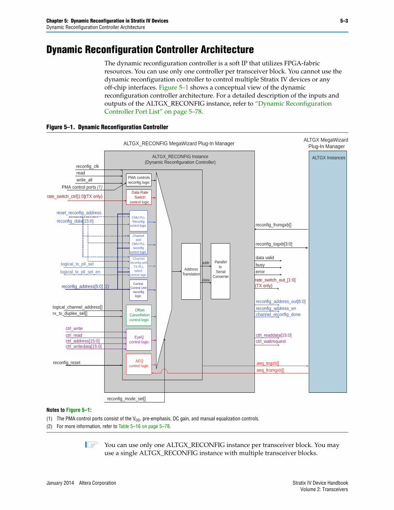
Chapter 5: Dynamic Reconfiguration in Stratix IV Devices 5–3Dynamic Reconfiguration Controller Architecture
Dynamic Reconfiguration Controller ArchitectureThe dynamic reconfiguration controller is a soft IP that utilizes FPGA-fabric resources. You can use only one controller per transceiver block. You cannot use the dynamic reconfiguration controller to control multiple Stratix IV devices or any off-chip interfaces. Figure 5–1 shows a conceptual view of the dynamic reconfiguration controller architecture. For a detailed description of the inputs and outputs of the ALTGX_RECONFIG instance, refer to “Dynamic Reconfiguration Controller Port List” on page 5–78.
1 You can use only one ALTGX_RECONFIG instance per transceiver block. You may use a single ALTGX_RECONFIG instance with multiple transceiver blocks.
Figure 5–1. Dynamic Reconfiguration Controller
Notes to Figure 5–1:
(1) The PMA control ports consist of the VOD, pre-emphasis, DC gain, and manual equalization controls.(2) For more information, refer to Table 5–16 on page 5–78.
CMU PLLReconfig
control logic
Data RateSwitch
control logic
OffsetCancellationcontrol logic
Channelreconfig with
TX PLLselect
control logic
Channeland
CMU PLLreconfig
control logic
rate_switch_ctrl[1:0](TX only)
reconfig_data[15:0]
logical_tx_pll_sel
reconfig_address_out[6:0]
rate_switch_out_[1:0](TX only)
reset_reconfig_address
EyeQ control logic
AEQcontrol logic
Central Control Unit
reconfiglogic
ctrl_write
ctrl_waitrequest
aeq_fromgxb[]
ALTGX_RECONFIG MegaWizard Plug-In Manager
ALTGX_RECONFIG Instance(Dynamic Reconfiguration Controller)
reconfig_clkread
write_all
PMA control ports (1)
logical_tx_pll_sel_en
logical_channel_address[]rx_tx_duplex_sel[]
ctrl_readctrl_address[15:0]ctrl_writedata[15:0]
reconfig_mode_sel[]
aeq_togxb[]
ctrl_readdata[15:0]
reconfig_address_enchannel_reconfig_done
errorbusy
data valid
reconfig_togxb[3:0]
reconfig_fromgxb[]
ALTGX MegaWizard Plug-In Manager
ALTGX Instances
Parallelto
SerialConverter
addr
data
AddressTranslation
PMA controlsreconfig logic
reconfig_address[5:0] (2)
reconfig_reset
January 2014 Altera Corporation Stratix IV Device HandbookVolume 2: Transceivers
5–4 Chapter 5: Dynamic Reconfiguration in Stratix IV DevicesQuartus II MegaWizard Plug-In Manager Interfaces to Support Dynamic Reconfiguration
Quartus II MegaWizard Plug-In Manager Interfaces to Support Dynamic Reconfiguration
Stratix IV GX devices provide two MegaWizard Plug-In Manager interfaces to support dynamic reconfiguration—ALTGX and ALTGX_RECONFIG.
ALTGX MegaWizard Plug-In ManagerUse the ALTGX MegaWizard Plug-In manager to enable the dynamic reconfiguration settings for the transceiver instances.
f For more information, refer to the “Reconfiguration Settings” section of the ALTGX Transceiver Setup Guide for Stratix IV Devices chapter.
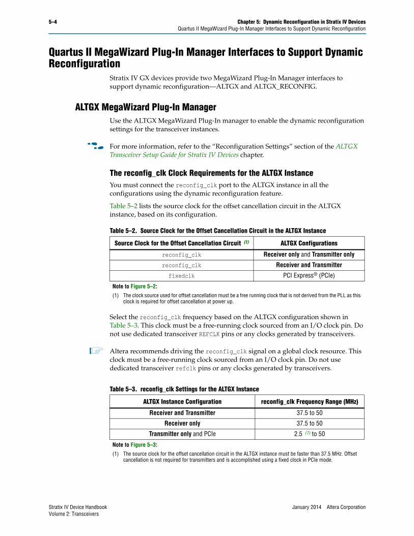
The reconfig_clk Clock Requirements for the ALTGX InstanceYou must connect the reconfig_clk port to the ALTGX instance in all the configurations using the dynamic reconfiguration feature.
Table 5–2 lists the source clock for the offset cancellation circuit in the ALTGX instance, based on its configuration.
Select the reconfig_clk frequency based on the ALTGX configuration shown in Table 5–3. This clock must be a free-running clock sourced from an I/O clock pin. Do not use dedicated transceiver REFCLK pins or any clocks generated by transceivers.
1 Altera recommends driving the reconfig_clk signal on a global clock resource. This clock must be a free-running clock sourced from an I/O clock pin. Do not use dedicated transceiver refclk pins or any clocks generated by transceivers.
Table 5–2. Source Clock for the Offset Cancellation Circuit in the ALTGX Instance
Source Clock for the Offset Cancellation Circuit (1) ALTGX Configurations
reconfig_clk Receiver only and Transmitter only
reconfig_clk Receiver and Transmitter
fixedclk PCI Express® (PCIe)
Note to Figure 5–2:
(1) The clock source used for offset cancellation must be a free running clock that is not derived from the PLL as this clock is required for offset cancellation at power up.
Table 5–3. reconfig_clk Settings for the ALTGX Instance
ALTGX Instance Configuration reconfig_clk Frequency Range (MHz)
Receiver and Transmitter 37.5 to 50
Receiver only 37.5 to 50
Transmitter only and PCIe 2.5 (1) to 50
Note to Figure 5–3:
(1) The source clock for the offset cancellation circuit in the ALTGX instance must be faster than 37.5 MHz. Offset cancellation is not required for transmitters and is accomplished using a fixed clock in PCIe mode.
Stratix IV Device Handbook January 2014 Altera CorporationVolume 2: Transceivers
Chapter 5: Dynamic Reconfiguration in Stratix IV Devices 5–5Quartus II MegaWizard Plug-In Manager Interfaces to Support Dynamic Reconfiguration
ALTGX_RECONFIG MegaWizard Plug-In ManagerUse the ALTGX_RECONFIG MegaWizard Plug-In Manager to instantiate the dynamic reconfiguration controller.
f For more information, refer to the Stratix IV ALTGX_RECONFIG Megafunction User Guide.
The reconfig_clk Clock Requirements for the ALTGX_RECONFIG InstanceYou must connect the reconfig_clk input port of the ALTGX_RECONFIG instance to the same clock that is connected to the reconfig_clk input port of the ALTGX instance.
Table 5–3 on page 5–4 lists the range of frequency values allowed for the reconfig_clk input port for the Receiver only, Receiver and Transmitter, and Transmitter only configuration modes of the ALTGX instance.
Based on the ALTGX configurations (Receiver only, Transmitter only, and Receiver and Transmitter) controlled by the ALTGX_RECONFIG instance, select the fastest reconfig_clk frequency value. This satisfies both the offset cancellation control for the receiver channels and the dynamic reconfiguration of the transmitter and receiver channels.
Interfacing ALTGX and ALTGX_RECONFIG InstancesTo dynamically reconfigure the transceiver channel, you must understand the concepts related to interfacing the transceivers with the dynamic reconfiguration controller. These concepts are:
■ “Logical Channel Addressing” on page 5–5
■ “Total Number of Channels Option in the ALTGX_RECONFIG Instance” on page 5–10
■ “Connecting the ALTGX and ALTGX_RECONFIG Instances” on page 5–11
Logical Channel Addressing The dynamic reconfiguration controller identifies a transceiver channel by using the logical channel address. The What is the starting channel number? option in the ALTGX MegaWizard Plug-In Manager allows you to set the logical channel address of all the channels within the ALTGX instance.
For channel reconfiguration with transmitter PLL select mode, the logical channel addressing concept extends to transmitter PLLs. For more information, refer to “Logical Channel Addressing When Using Additional PLLs” on page 5–52.
The following sections describe the concept of logical channel addressing for ALTGX instances configured with:
■ Regular transceiver channels (PCS and PMA channels)
■ PMA-only channels
■ A combination of PMA-only channels and regular transceiver channels
January 2014 Altera Corporation Stratix IV Device HandbookVolume 2: Transceivers
5–6 Chapter 5: Dynamic Reconfiguration in Stratix IV DevicesQuartus II MegaWizard Plug-In Manager Interfaces to Support Dynamic Reconfiguration
Logical Channel Addressing of Regular Transceiver Channels
For a single ALTGX instance connected to the dynamic reconfiguration controller, set the starting channel number to 0. The logical channel addresses of the first channel within the ALTGX instance is 0. The logical channel addresses of the remaining channels increment by one.
For multiple ALTGX instances connected to the dynamic reconfiguration controller, set the starting channel number of the first instance to 0. For the starting channel number for the following ALTGX instances, you must set the next multiple of four. The logical channel address of channels within each ALTGX instance increment by one.
Figure 5–2 shows how to set the starting channel number for multiple ALTGX instances controlled by a single dynamic reconfiguration controller, where both ALTGX instances have regular transceiver channels.
Figure 5–2. Logical Channel Addressing of Regular Transceiver Channels
Notes to Figure 5–2:
(1) For more information, refer to “Total Number of Channels Option in the ALTGX_RECONFIG Instance” on page 5–10.(2) reconfig_fromgxb[50:0] = { reconfig_fromgxb 2[16:0], reconfig_fromgxb 1[33:0]}.
ALTGX instance 1 Five regular transceiver channels
Basic Functional ModeStarting channel number = 0
ALTGX instance 2Two regular transceiver channels
Basic Functional Mode Starting channel number = 8
Channel 1 (logical channel address = 9)
reconfig_togx
Channel 0 (logical channel address = 0)
Channel 1 (logical channel address = 1)
Channel 2 (logical channel address = 2
Channel 3 (logical channel address = 3)
Channel 4 (logical channel address = 4)
Channel 0 (logical channel address = 8)
reconfig_fromgxb 1[33:0]
reconfig_fromgxb 2[16:0]
Set the What is the number ofchannels controlled by the
reconfig controller? option to 12 (1)
reconfig_fromgxb[50:0] (2)
ALTGX_RECONFIG Instance 1
Stratix IV Device Handbook January 2014 Altera CorporationVolume 2: Transceivers
Chapter 5: Dynamic Reconfiguration in Stratix IV Devices 5–7Quartus II MegaWizard Plug-In Manager Interfaces to Support Dynamic Reconfiguration
Logical Channel Addressing of PMA-Only Channels
1 CMU channels are always PMA-only channels. The regular transceiver channels can be optionally configured as PMA-only channels.
Set the starting channel number for the PMA-only channels in the What is the starting channel number? option in the ALTGX MegaWizard Plug-In Manager.
For a single ALTGX instance connected to the dynamic reconfiguration controller, set the starting channel number to 0. The logical channel address of the first channel in the ALTGX instance is 0. The logical channel addresses of the PMA-only channels within the same ALTGX instance increment in multiples of four (unlike the logical channel addressing of regular transceiver channels that are not configured in Basic [PMA Direct] functional mode, where the logical channel address increments in steps of one within the same ALTGX instance).
For multiple ALTGX instances connected to the dynamic reconfiguration controller, set the starting channel number of the first instance to 0. You must set the next multiple of four as the starting channel number for the remaining ALTGX instances.
1 When PMA-only channel reconfiguration involves a transmitter PLL, you also must account for the logical channel address of the PLL used. If there are four channels in Basic [PMA Direct] ×N functional mode, each channel requires a logical channel address (0, 4, 8, 12), and the transmitter PLL used requires an address (16).
Figure 5–3 shows how to set the starting channel number for multiple ALTGX instances controlled by a single dynamic reconfiguration controller, where both ALTGX instances have PMA-only channels. For more information about the What is the number of channels controlled by the reconfig controller? option, refer to “Total Number of Channels Option in the ALTGX_RECONFIG Instance” on page 5–10.
January 2014 Altera Corporation Stratix IV Device HandbookVolume 2: Transceivers
5–8 Chapter 5: Dynamic Reconfiguration in Stratix IV DevicesQuartus II MegaWizard Plug-In Manager Interfaces to Support Dynamic Reconfiguration
For example, if you a transceiver configuration with Instance 1 (Inst1) with two channels that use Basic (PMA Direct) mode. Instance 2 (Inst2) has two channels and uses Basic mode, which uses the PCS block in the transceiver. In order to leave the needed gap in the reconfiguration controller signals, follow these steps:
1. Set Inst1 to have a starting channel number 0. The logical channel addresses 0 and 4 are then allocated to the two channels of Inst1.
2. Reserve logical channel address 8—do not use this address.
3. Set Inst2 to have a starting channel number 12.
Figure 5–3. Logical Channel Addressing of PMA-Only Channels
Note to Figure 5–3:
(1) reconfig_fromgxb[203:0] = { reconfig_fromgxb 2[67:0], reconfig_fromgxb 1[135:0]}.
Starting channel number = 0
ALTGX_RECONFIG Instance 1
reconfig_togxb[3:0]
Channel 0(logical channel address = 0)
Set the What is the number ofchannels controlled by the
reconfig controller? option to 48
reconfig_fromgxb 1[135:0]
reconfig_fromgxb 2[67:0]
reconfig_fromgxb[203:0] (1)
ALTGX Instance 1Basic (PMA Direct) Configuration
Channel 1(logical channel address = 4)
Channel 2(logical channel address = 8)
Channel 3(logical channel address = 12)
Channel 4(logical channel address = 16)
Channel 5(logical channel address = 20)
Channel 6(logical channel address = 24)
Channel 7(logical channel address = 28)
Starting channel number = 32
ALTGX Instance 2Basic (PMA Direct) Configuration
Channel 0(logical channel address = 32)
Channel 1(logical channel address = 36
Channel 2(logical channel address = 40)
Channel 3(logical channel address = 44)
Stratix IV Device Handbook January 2014 Altera CorporationVolume 2: Transceivers
Chapter 5: Dynamic Reconfiguration in Stratix IV Devices 5–9Quartus II MegaWizard Plug-In Manager Interfaces to Support Dynamic Reconfiguration
4. Set the Number of channels option in the ALTGX_RECONFIG controller megafunction to the nearest multiple of four from the highest logical channel address. In this example, set the Number of channels option to 16.
5. When connecting the reconfig_fromgxb bus of the ALTGX_RECONFIG controller, connect the bits corresponding to the reserved address to 0. In this example, the ALTGX_RECONFIG controller provides 4*([16:0]) bits.
6. Connect the reconfig_fromgxb bus of the ALTGX_RECONIF controller and the ALTGX transceiver instances as follows:
a. reconfig_fromgxb[33:0] of the ALTGX_RECONFIG instance - reconfig_fromgxb[33:0] of Inst1.
b. reconfig_fromgxb[50:34] of the ALTGX_RECONFIG instance - 17’h00000
c. reconfig_fromgxb[67:51] of the ALTGX_RECONFIG instance - reconfig_fromgxb[17:0] of Inst2
Logical Channel Addressing—Combination of Regular Transceiver Channels and PMA-Only Channels
For a combination of regular transceiver channels and PMA-only channels, there must be at least two different ALTGX instances connected to the same dynamic reconfiguration controller. This is because you cannot have a combination of regular transceiver channels and PMA-only channels within the same ALTGX instance.
Set the starting channel number in the first ALTGX Instance 1 to 0. If you have configured ALTGX Instance 1 with regular transceiver channels, the logical channel addresses of the remaining channels increment in steps of one.
Set the starting channel number of the following ALTGX Instance 2 as the next multiple of four. If you have configured ALTGX Instance 2 with PMA-only channels, the logical channel addresses of the remaining channels increment in steps of four.
Figure 5–41 in “Example 1” on page 5–96 shows how to set the starting channel number for multiple ALTGX instances controlled by a single dynamic reconfiguration controller, where one ALTGX instance has PMA-only channels and the other ALTGX instance has regular transceiver channels.
Table 5–18 in “Example 1” on page 5–96 lists an example scenario where the logical channel address of both the PMA-only channels and regular transceiver channels is set based on the starting channel number.
For more information, refer to “Example 1” on page 5–96.
Highest Possible Logical Channel Address
Table 5–4 lists the highest possible logical channel address assigned to a transceiver channel in a Stratix IV device.
The maximum number of transceiver channels in the largest Stratix IV device is 48 (24 transceiver channels located in four transceiver blocks on the right side of the device and 24 transceiver channels located in four transceiver blocks on the left side of the device).
You can individually configure these 48 transceiver channels as 48 Transmitter only and 48 Receiver only channels. You achieve this by using 48 Transmitter only ALTGX instances and 48 Receiver only ALTGX instances in your design.
January 2014 Altera Corporation Stratix IV Device HandbookVolume 2: Transceivers
5–10 Chapter 5: Dynamic Reconfiguration in Stratix IV DevicesQuartus II MegaWizard Plug-In Manager Interfaces to Support Dynamic Reconfiguration
The highest logical channel address is assigned to the Receiver only channel in the 96th ALTGX instance; therefore, the setting is 380.
1 The highest possible logical channel address assigned to a transceiver channel in a Stratix IV device is the same whether the channel is a regular transceiver channel or a PMA-only channel.
Total Number of Channels Option in the ALTGX_RECONFIG InstanceYou can connect every dynamic reconfiguration controller in a design to either a single ALTGX instance or to multiple ALTGX instances. Depending on the number of channels within each of these ALTGX instances, you must set the total number of channels controlled by the dynamic reconfiguration controller in the ALTGX_RECONFIG MegaWizard Plug-In Manager. Based on this information, the reconfig_fromgxb and logical_channel_address input ports vary in width.
Use the following steps to determine the number of channels:
1. Determine the highest logical channel address among all the transceiver instances connected to the same dynamic reconfiguration controller. For more information, refer to “Logical Channel Addressing” on page 5–5.
2. Round the logical channel address value to the next higher multiple of four.
3. Use this value to set the What is the number of channels controlled by the reconfig controller? option.
For more information, refer to “Example 1” on page 5–96.
Table 5–4. Highest Possible Logical Channel Address
96 ALTGX Instances ALTGX_RECONFIG Instance
ALTGX MegaWizard Plug-In Manager Setting ALTGX instance 1 ALTGX instance 2
ALTGX_RECONFIG instance 1:
Controls all 96 ALTGX instances.
What is the number of channels? in the General screen
48 48
What is the starting channel number? in the Reconfig screen
TX instance 1: 0
TX instance 2: 4
.
.
.
.
.
.
TX instance 48: 188
RX instance 1: 192
RX instance 2: 196
.
.
.
.
.
.
RX instance 48: 380
Stratix IV Device Handbook January 2014 Altera CorporationVolume 2: Transceivers
Chapter 5: Dynamic Reconfiguration in Stratix IV Devices 5–11Quartus II MegaWizard Plug-In Manager Interfaces to Support Dynamic Reconfiguration
Connecting the ALTGX and ALTGX_RECONFIG InstancesThere are two ways to connect the ALTGX_RECONFIG instance to the ALTGX instance in your design:
■ Single dynamic reconfiguration controller—You can use a single ALTGX_RECONFIG instance to control all the ALTGX instances in your design. Figure 5–2 on page 5–6 shows a block diagram of a single dynamic reconfiguration controller in a design.
■ Multiple dynamic reconfiguration controllers—Your design can have multiple ALTGX_RECONFIG instances but you can use only one ALTGX_RECONFIG instance per transceiver block, as shown in Figure 5–4.
In the dynamic reconfiguration interface, you must connect the reconfig_fromgxb and reconfig_togxb signals between the ALTGX_RECONFIG instance and the ALTGX instance to successfully complete the dynamic reconfiguration process. Make the following connections:
■ Connect the reconfig_fromgxb input port of the ALTGX_RECONFIG instance to the reconfig_fromgxb output ports of all the ALTGX instances controlled by the ALTGX_RECONFIG instance.
■ Connect the reconfig_fromgxb port of the ALTGX instance whose starting channel number is 0, to the lowest significant bit of the reconfig_fromgxb input port of the ALTGX_RECONFIG instance.
■ Connect the reconfig_fromgxb port of the ALTGX instance with the next highest starting channel number to the following bits of the reconfig_fromgxb of the ALTGX_RECONFIG instance, and so on.
■ Connect the same reconfig_togxb ports of all the ALTGX instances controlled by the ALTGX_RECONFIG instance to the reconfig_togxb output port of the ALTGX_RECONFIG instance. The reconfig_togxb output port is fixed to 4 bits.
Figure 5–4. Multiple Dynamic Reconfiguration Controllers in a Design
ALTGX Instance 1ALTGX_RECONFIG Instance 1
reconfig_fromgxb [n:0]
reconfig_togxb [3:0]
ALTGX Instance 2ALTGX_RECONFIG Instance 2
reconfig_fromgxb [n:0]
reconfig_togxb [3:0]
January 2014 Altera Corporation Stratix IV Device HandbookVolume 2: Transceivers
5–12 Chapter 5: Dynamic Reconfiguration in Stratix IV DevicesDynamic Reconfiguration Modes Implementation
Connecting reconfig_fromgxb for the Regular Transceiver Channels
Figure 5–3 on page 5–8 shows how to connect the reconfig_fromgxb output port of the ALTGX instance to the reconfig_fromgxb input port of the ALTGX_RECONFIG instance for regular transceiver channels.
Table 5–18 in “Example 1” on page 5–96 describes how to connect the reconfig_fromgxb port for regular transceiver channels.
Connecting reconfig_fromgxb for the PMA-Only Channels
Figure 5–3 on page 5–8 shows how to connect the reconfig_fromgxb output port of the ALTGX instance to the reconfig_fromgxb input port of the ALTGX_RECONFIG instance for PMA-only channels.
Table 5–18 in “Example 1” on page 5–96 describes how to connect the reconfig_fromgxb port for PMA-Only channels.
Dynamic Reconfiguration Modes ImplementationThe modes available for dynamically reconfiguring the Stratix IV transceivers are:
■ “PMA Controls Reconfiguration Mode Details” on page 5–12
■ “Transceiver Channel Reconfiguration Mode Details” on page 5–19
■ Channel and CMU PLL reconfiguration (.mif based)
■ Channel reconfiguration with transmitter PLL select (.mif based)
■ CMU PLL reconfiguration (.mif based)
■ Central control unit reconfiguration (.mif based)
■ Data rate division in transmitter
■ “Offset Cancellation Feature” on page 5–67
■ “EyeQ” on page 5–69
■ “Adaptive Equalization (AEQ)” on page 5–75
■ “Dynamic Reconfiguration Controller Port List” on page 5–78
The following sections describe each of these modes in detail.
PMA Controls Reconfiguration Mode DetailsYou can dynamically reconfigure the following PMA controls:
■ Pre-emphasis settings
■ DC gain settings
■ Voltage output differential (VOD) settings
■ Equalization settings (channel reconfiguration mode does not support equalization settings)
The following section describes how to connect the transceiver channels (the ALTGX instance) to the dynamic reconfiguration controller (the ALTGX_RECONFIG instance) to dynamically reconfigure the PMA controls.
Stratix IV Device Handbook January 2014 Altera CorporationVolume 2: Transceivers
Chapter 5: Dynamic Reconfiguration in Stratix IV Devices 5–13Dynamic Reconfiguration Modes Implementation
The PMA control ports for the ALTGX_RECONFIG MegaWizard Plug-In Manager are available in the Analog controls screen. You can select the PMA control ports you want to reconfigure. For example, to use tx_vodctrl to write new VOD settings or to use tx_vodctrl_out to read the existing VOD settings.
Dynamically Reconfiguring PMA ControlsYou can dynamically reconfigure the PMA controls of a transceiver channel using three methods:
■ Reconfiguring the PMA controls of a specific transceiver channel. For more information, refer to “Method 1—Using the logical_channel_address Port”.
■ Dynamically reconfiguring the PMA controls of the transceiver channels without using the logical_channel_address port (where all transceiver channels are reconfigured). If you use this method, the PMA controls of all the transceiver channels connected to the dynamic reconfiguration controller are reconfigured. For more information, refer to “Method 2—Using the Same Control Signals for All Channels” on page 5–15.
■ Dynamically reconfiguring the PMA controls of the transceiver channels without using the logical_channel_address port (where only the PMA controls of the transceiver channels are reconfigured). If you use this method, each channel has its own PMA control port. Based on the value set at the ports, the PMA controls of the corresponding transceiver channels are reconfigured. For more information, refer to “Method 3—Using Individual Control Signals for Each Channel” on page 5–17.
For the above three methods, you can additionally use the rx_tx_duplex_sel[1:0] port transmitter and receiver parameters. For more information, refer to “Dynamic Reconfiguration Controller Port List” on page 5–78.
Method 1—Using the logical_channel_address Port
Using Method 1, you can dynamically reconfigure the PMA controls of a transceiver channel by using the logical_channel_address port without affecting the remaining active channels. Enable the logical_channel_address port by selecting the Use 'logical_channel_address' port for Analog controls reconfiguration option in the Analog controls screen of the ALTGX_RECONFIG MegaWizard Plug-In Manager.
1 This method is applicable only for a design where the dynamic reconfiguration controller controls more than one channel.
When using Method 1, the selected PMA control write and read ports remain fixed in width, regardless of the number of channels controlled by the ALTGX_RECONFIG instance.
To observe the width of the PMA control ports, refer to the ALTGX_RECONFIG MegaWizard Plug-In Manager.
The value you set at the PMA control ports is only written into the specified transceiver channel.
1 Ensure that the busy signal is low before you start a write or read transaction. The busy output status signal is asserted high when the dynamic reconfiguration controller is occupied writing or reading the PMA control values. When the write or read transaction has completed, the busy signal goes low.
January 2014 Altera Corporation Stratix IV Device HandbookVolume 2: Transceivers
5–14 Chapter 5: Dynamic Reconfiguration in Stratix IV DevicesDynamic Reconfiguration Modes Implementation
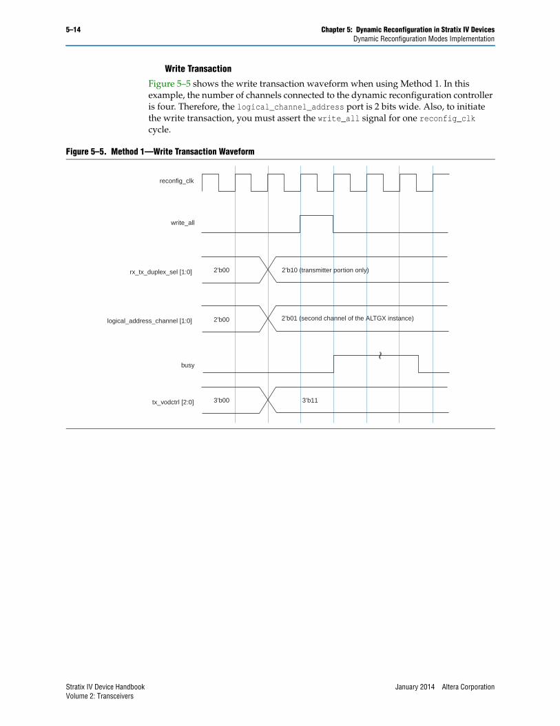
Write Transaction
Figure 5–5 shows the write transaction waveform when using Method 1. In this example, the number of channels connected to the dynamic reconfiguration controller is four. Therefore, the logical_channel_address port is 2 bits wide. Also, to initiate the write transaction, you must assert the write_all signal for one reconfig_clk cycle.
Figure 5–5. Method 1—Write Transaction Waveform
reconfig_clk
rx_tx_duplex_sel [1:0]
write_all
2’b00 2’b10 (transmitter portion only)
2’b01 (second channel of the ALTGX instance)2’b00
3’b00 3’b11
busy
tx_vodctrl [2:0]
logical_address_channel [1:0]
Stratix IV Device Handbook January 2014 Altera CorporationVolume 2: Transceivers
Chapter 5: Dynamic Reconfiguration in Stratix IV Devices 5–15Dynamic Reconfiguration Modes Implementation
Read Transaction
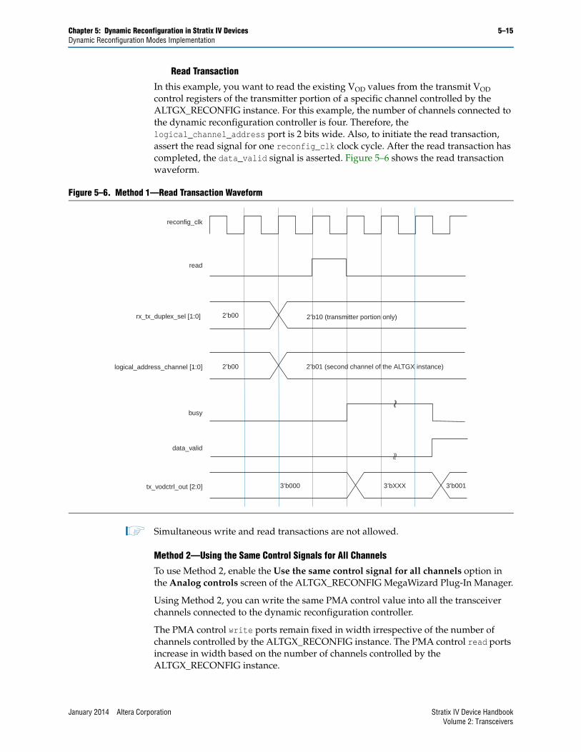
In this example, you want to read the existing VOD values from the transmit VOD control registers of the transmitter portion of a specific channel controlled by the ALTGX_RECONFIG instance. For this example, the number of channels connected to the dynamic reconfiguration controller is four. Therefore, the logical_channel_address port is 2 bits wide. Also, to initiate the read transaction, assert the read signal for one reconfig_clk clock cycle. After the read transaction has completed, the data_valid signal is asserted. Figure 5–6 shows the read transaction waveform.
1 Simultaneous write and read transactions are not allowed.
Method 2—Using the Same Control Signals for All Channels
To use Method 2, enable the Use the same control signal for all channels option in the Analog controls screen of the ALTGX_RECONFIG MegaWizard Plug-In Manager.
Using Method 2, you can write the same PMA control value into all the transceiver channels connected to the dynamic reconfiguration controller.
The PMA control write ports remain fixed in width irrespective of the number of channels controlled by the ALTGX_RECONFIG instance. The PMA control read ports increase in width based on the number of channels controlled by the ALTGX_RECONFIG instance.
Figure 5–6. Method 1—Read Transaction Waveform
reconfig_clk
rx_tx_duplex_sel [1:0]
read
2’b00 2’b10 (transmitter portion only)
2’b01 (second channel of the ALTGX instance)2’b00
3’b000 3’b0013’bXXX
busy
tx_vodctrl_out [2:0]
logical_address_channel [1:0]
data_valid
January 2014 Altera Corporation Stratix IV Device HandbookVolume 2: Transceivers
5–16 Chapter 5: Dynamic Reconfiguration in Stratix IV DevicesDynamic Reconfiguration Modes Implementation
Write Transaction
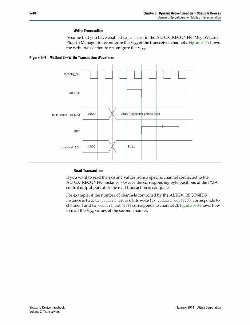
Assume that you have enabled tx_vodctrl in the ALTGX_RECONFIG MegaWizard Plug-In Manager to reconfigure the VOD of the transceiver channels. Figure 5–7 shows the write transaction to reconfigure the VOD.
Read Transaction
If you want to read the existing values from a specific channel connected to the ALTGX_RECONFIG instance, observe the corresponding byte positions of the PMA control output port after the read transaction is complete.
For example, if the number of channels controlled by the ALTGX_RECONFIG instance is two, tx_vodctrl_out is 6 bits wide (tx_vodctrl_out[2:0] corresponds to channel 1 and tx_vodctrl_out[5:3] corresponds to channel 2). Figure 5–8 shows how to read the VOD values of the second channel.
Figure 5–7. Method 2—Write Transaction Waveform
reconfig_clk
rx_tx_duplex_sel [1:0]
write_all
2’b00 2’b10 (transmitter portion only)
3’b00 3’b11
busy
tx_vodctrl [2:0]
Stratix IV Device Handbook January 2014 Altera CorporationVolume 2: Transceivers
Chapter 5: Dynamic Reconfiguration in Stratix IV Devices 5–17Dynamic Reconfiguration Modes Implementation
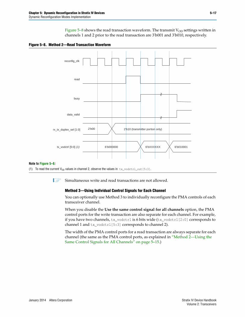
Figure 5–8 shows the read transaction waveform. The transmit VOD settings written in channels 1 and 2 prior to the read transaction are 3'b001 and 3'b010, respectively.
1 Simultaneous write and read transactions are not allowed.
Method 3—Using Individual Control Signals for Each Channel
You can optionally use Method 3 to individually reconfigure the PMA controls of each transceiver channel.
When you disable the Use the same control signal for all channels option, the PMA control ports for the write transaction are also separate for each channel. For example, if you have two channels, tx_vodctrl is 6 bits wide (tx_vodctrl[2:0] corresponds to channel 1 and tx_vodctrl[5:3] corresponds to channel 2).
The width of the PMA control ports for a read transaction are always separate for each channel (the same as the PMA control ports, as explained in “Method 2—Using the Same Control Signals for All Channels” on page 5–15.)
Figure 5–8. Method 2—Read Transaction Waveform
Note to Figure 5–8:
(1) To read the current VOD values in channel 2, observe the values in tx_vodctrl_out[5:3].
reconfig_clk
rx_tx_duplex_sel [1:0]
read
2’b00 2’b10 (transmitter portion only)
6’bXXXXXX 6’b0100016’b000000
busy
tx_vodctrl [5:0] (1)
data_valid
January 2014 Altera Corporation Stratix IV Device HandbookVolume 2: Transceivers
5–18 Chapter 5: Dynamic Reconfiguration in Stratix IV DevicesDynamic Reconfiguration Modes Implementation
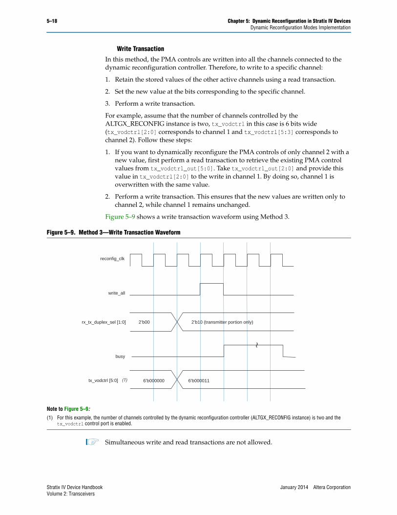
Write Transaction
In this method, the PMA controls are written into all the channels connected to the dynamic reconfiguration controller. Therefore, to write to a specific channel:
1. Retain the stored values of the other active channels using a read transaction.
2. Set the new value at the bits corresponding to the specific channel.
3. Perform a write transaction.
For example, assume that the number of channels controlled by the ALTGX_RECONFIG instance is two, tx_vodctrl in this case is 6 bits wide (tx_vodctrl[2:0] corresponds to channel 1 and tx_vodctrl[5:3] corresponds to channel 2). Follow these steps:
1. If you want to dynamically reconfigure the PMA controls of only channel 2 with a new value, first perform a read transaction to retrieve the existing PMA control values from tx_vodctrl_out[5:0]. Take tx_vodctrl_out[2:0] and provide this value in tx_vodctrl[2:0] to the write in channel 1. By doing so, channel 1 is overwritten with the same value.
2. Perform a write transaction. This ensures that the new values are written only to channel 2, while channel 1 remains unchanged.
Figure 5–9 shows a write transaction waveform using Method 3.
1 Simultaneous write and read transactions are not allowed.
Figure 5–9. Method 3—Write Transaction Waveform
Note to Figure 5–9:
(1) For this example, the number of channels controlled by the dynamic reconfiguration controller (ALTGX_RECONFIG instance) is two and the tx_vodctrl control port is enabled.
reconfig_clk
(1)
rx_tx_duplex_sel [1:0]
write_all
2’b00 2’b10 (transmitter portion only)
6’b0000116’b000000
busy
tx_vodctrl [5:0]
Stratix IV Device Handbook January 2014 Altera CorporationVolume 2: Transceivers
Chapter 5: Dynamic Reconfiguration in Stratix IV Devices 5–19Dynamic Reconfiguration Modes Implementation
Read Transaction
The read transaction in Method 3 is identical to that in Method 2. Refer to “Read Transaction” on page 5–16.
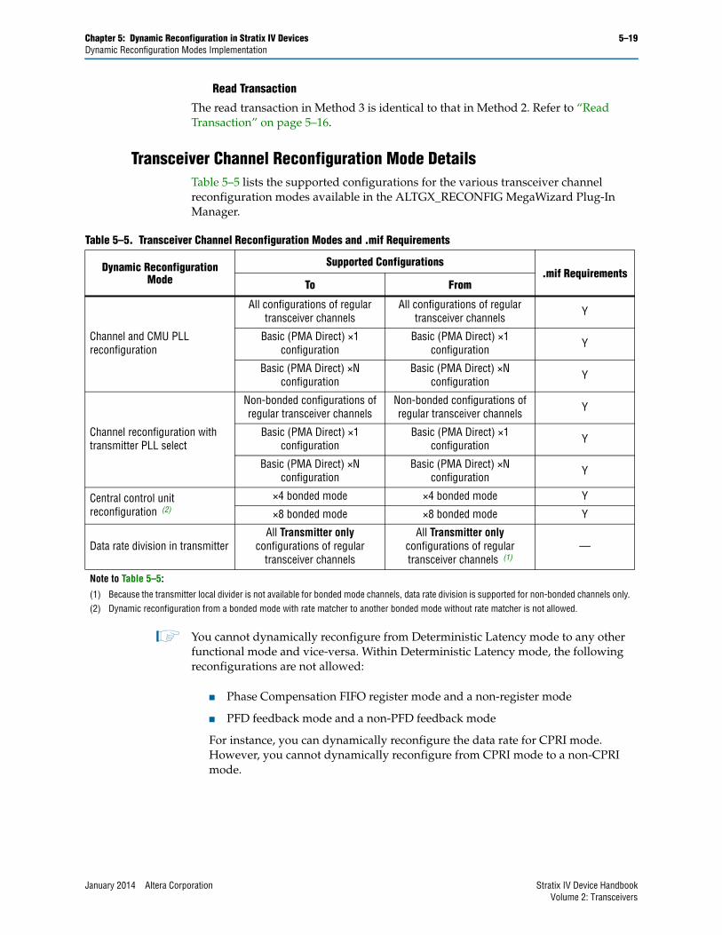
Transceiver Channel Reconfiguration Mode DetailsTable 5–5 lists the supported configurations for the various transceiver channel reconfiguration modes available in the ALTGX_RECONFIG MegaWizard Plug-In Manager.
1 You cannot dynamically reconfigure from Deterministic Latency mode to any other functional mode and vice-versa. Within Deterministic Latency mode, the following reconfigurations are not allowed:
■ Phase Compensation FIFO register mode and a non-register mode
■ PFD feedback mode and a non-PFD feedback mode
For instance, you can dynamically reconfigure the data rate for CPRI mode. However, you cannot dynamically reconfigure from CPRI mode to a non-CPRI mode.
Table 5–5. Transceiver Channel Reconfiguration Modes and .mif Requirements
Dynamic Reconfiguration Mode
Supported Configurations.mif Requirements
To From
Channel and CMU PLL reconfiguration
All configurations of regular transceiver channels
All configurations of regular transceiver channels Y
Basic (PMA Direct) ×1 configuration
Basic (PMA Direct) ×1 configuration Y
Basic (PMA Direct) ×N configuration
Basic (PMA Direct) ×N configuration Y
Channel reconfiguration with transmitter PLL select
Non-bonded configurations of regular transceiver channels
Non-bonded configurations of regular transceiver channels Y
Basic (PMA Direct) ×1 configuration
Basic (PMA Direct) ×1 configuration Y
Basic (PMA Direct) ×N configuration
Basic (PMA Direct) ×N configuration Y
Central control unit reconfiguration (2)
×4 bonded mode ×4 bonded mode Y
×8 bonded mode ×8 bonded mode Y
Data rate division in transmitterAll Transmitter only
configurations of regular transceiver channels
All Transmitter only configurations of regular transceiver channels (1)
—
Note to Table 5–5:
(1) Because the transmitter local divider is not available for bonded mode channels, data rate division is supported for non-bonded channels only.(2) Dynamic reconfiguration from a bonded mode with rate matcher to another bonded mode without rate matcher is not allowed.
January 2014 Altera Corporation Stratix IV Device HandbookVolume 2: Transceivers
5–20 Chapter 5: Dynamic Reconfiguration in Stratix IV DevicesDynamic Reconfiguration Modes Implementation
Memory Initialization File (.mif)As listed in Table 5–5, all the dynamic reconfiguration modes with a check mark in the “.mif Requirement” column use memory initialization files to reconfigure the transceivers. These .mifs contain the valid settings, in the form of words, required to reconfigure the transceivers. To understand using .mifs, it is helpful to understand these two concepts:
■ How to generate a .mif?—The Quartus® II software generates .mifs when you provide the appropriate project settings and then compiles an ALTGX instance. For more information, refer to “Quartus II Settings to Enable .mif Generation” on page 5–20.
■ How is a .mif used between the ALTGX_RECONFIG instance and the ALTGX instance?—The Quartus II software provides a design flow called the user memory initialization file flow. For more information, refer to “.mif-Based Design Flow” on page 5–22.
Quartus II Settings to Enable .mif Generation
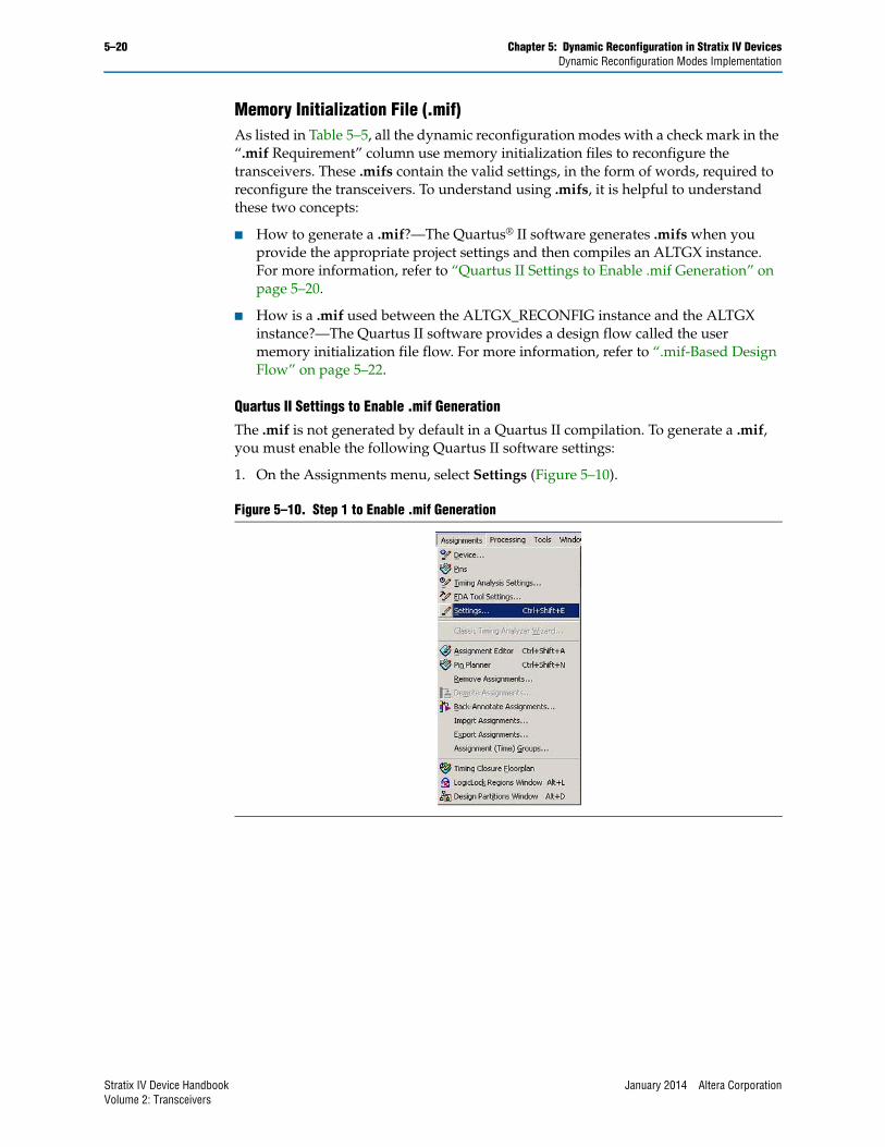
The .mif is not generated by default in a Quartus II compilation. To generate a .mif, you must enable the following Quartus II software settings:
1. On the Assignments menu, select Settings (Figure 5–10).
Figure 5–10. Step 1 to Enable .mif Generation
Stratix IV Device Handbook January 2014 Altera CorporationVolume 2: Transceivers
Chapter 5: Dynamic Reconfiguration in Stratix IV Devices 5–21Dynamic Reconfiguration Modes Implementation
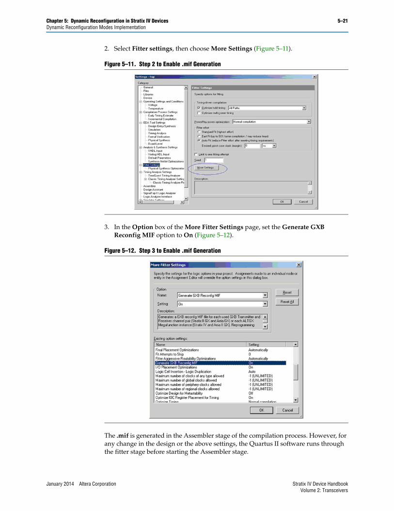
2. Select Fitter settings, then choose More Settings (Figure 5–11).
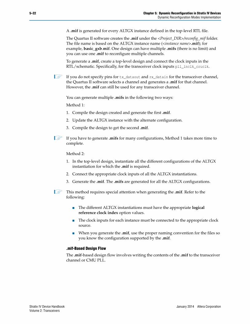
3. In the Option box of the More Fitter Settings page, set the Generate GXB Reconfig MIF option to On (Figure 5–12).
The .mif is generated in the Assembler stage of the compilation process. However, for any change in the design or the above settings, the Quartus II software runs through the fitter stage before starting the Assembler stage.
Figure 5–11. Step 2 to Enable .mif Generation
Figure 5–12. Step 3 to Enable .mif Generation
January 2014 Altera Corporation Stratix IV Device HandbookVolume 2: Transceivers
5–22 Chapter 5: Dynamic Reconfiguration in Stratix IV DevicesDynamic Reconfiguration Modes Implementation
A .mif is generated for every ALTGX instance defined in the top-level RTL file.
The Quartus II software creates the .mif under the <Project_DIR>/reconfig_mif folder. The file name is based on the ALTGX instance name (<instance name>.mif); for example, basic_gxb.mif. One design can have multiple .mifs (there is no limit) and you can use one .mif to reconfigure multiple channels.
To generate a .mif, create a top-level design and connect the clock inputs in the RTL/schematic. Specifically, for the transceiver clock inputs pll_inclk_cruclk.
1 If you do not specify pins for tx_dataout and rx_datain for the transceiver channel, the Quartus II software selects a channel and generates a .mif for that channel. However, the .mif can still be used for any transceiver channel.
You can generate multiple .mifs in the following two ways:
Method 1:
1. Compile the design created and generate the first .mif.
2. Update the ALTGX instance with the alternate configuration.
3. Compile the design to get the second .mif.
1 If you have to generate .mifs for many configurations, Method 1 takes more time to complete.
Method 2:
1. In the top-level design, instantiate all the different configurations of the ALTGX instantiation for which the .mif is required.
2. Connect the appropriate clock inputs of all the ALTGX instantiations.
3. Generate the .mif. The .mifs are generated for all the ALTGX configurations.
1 This method requires special attention when generating the .mif. Refer to the following:
■ The different ALTGX instantiations must have the appropriate logical reference clock index option values.
■ The clock inputs for each instance must be connected to the appropriate clock source.
■ When you generate the .mif, use the proper naming convention for the files so you know the configuration supported by the .mif.
.mif-Based Design Flow
The .mif-based design flow involves writing the contents of the .mif to the transceiver channel or CMU PLL.
Stratix IV Device Handbook January 2014 Altera CorporationVolume 2: Transceivers
Chapter 5: Dynamic Reconfiguration in Stratix IV Devices 5–23Dynamic Reconfiguration Modes Implementation
To reconfigure the transceiver channel or CMU PLL, you must configure the required settings for the transceiver channel or CMU PLL in the ALTGX MegaWizard Plug-In Manager and compile the ALTGX instance. The dynamic reconfiguration controller requires that you write these configured settings through the .mif into the transceiver channel or CMU PLL (using the write_all and reconfig_data[15:0] signals). The maximum possible size of the .mif is 59 words. Each word contains legal register settings of the transceiver channel stored in 16 bits. reconfig_address_out[5:0] provides the address (location) of the 16-bit word in the .mif.
Table 5–6 lists the .mif size depending on the ALTGX configuration.
You can store these .mifs in on-chip or off-chip memory.
Applying a .mif in the User Design
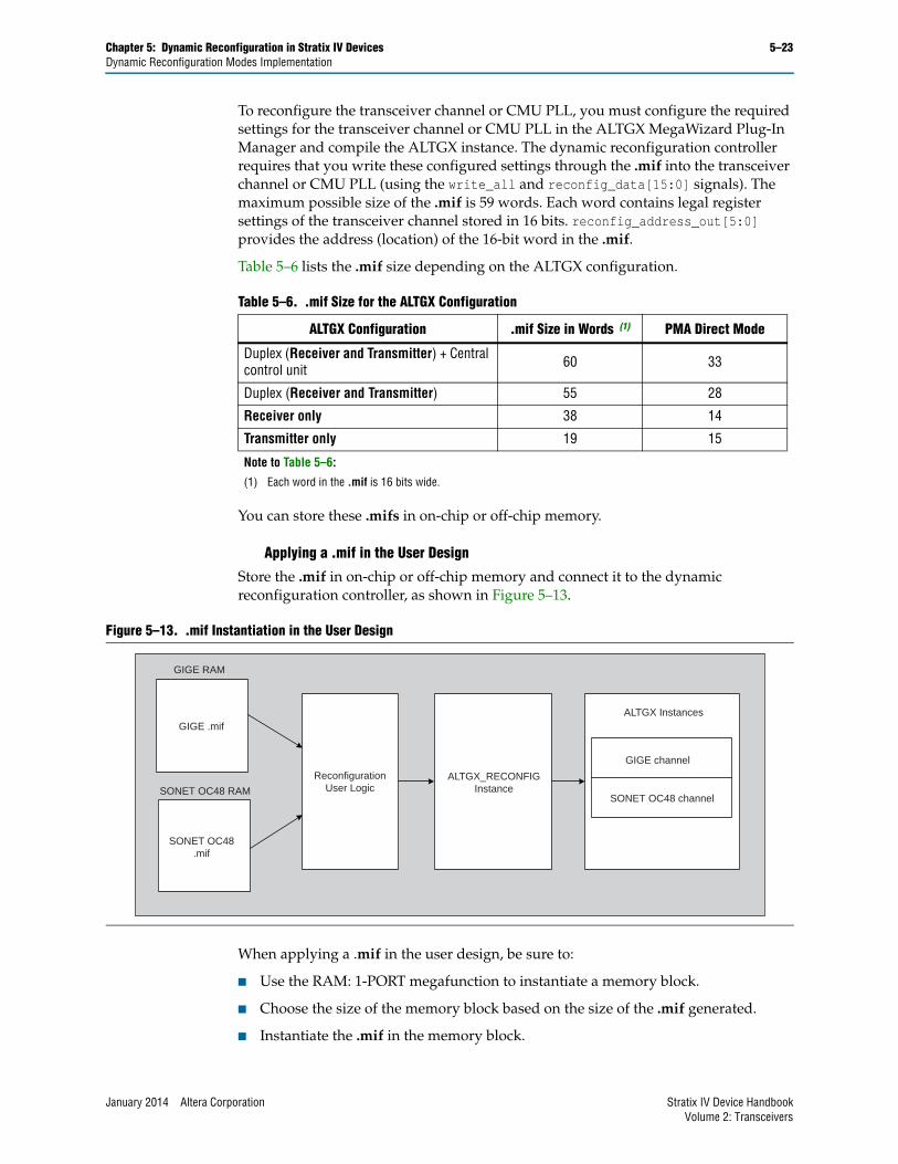
Store the .mif in on-chip or off-chip memory and connect it to the dynamic reconfiguration controller, as shown in Figure 5–13.
When applying a .mif in the user design, be sure to:
■ Use the RAM: 1-PORT megafunction to instantiate a memory block.
■ Choose the size of the memory block based on the size of the .mif generated.
■ Instantiate the .mif in the memory block.
Table 5–6. .mif Size for the ALTGX Configuration
ALTGX Configuration .mif Size in Words (1) PMA Direct Mode
Duplex (Receiver and Transmitter) + Central control unit 60 33
Duplex (Receiver and Transmitter) 55 28
Receiver only 38 14
Transmitter only 19 15
Note to Table 5–6:
(1) Each word in the .mif is 16 bits wide.
Figure 5–13. .mif Instantiation in the User Design
GIGE .mif
SONET OC48 RAM
SONET OC48.mif
ReconfigurationUser Logic
ALTGX_RECONFIGInstance
ALTGX Instances
GIGE channel
SONET OC48 channel
GIGE RAM
January 2014 Altera Corporation Stratix IV Device HandbookVolume 2: Transceivers
5–24 Chapter 5: Dynamic Reconfiguration in Stratix IV DevicesDynamic Reconfiguration Modes Implementation
1 Whenever a .mif is applied to a channel, the PMA controls for that channel are set to the default settings chosen in the ALTGX instance used for .mif generation.
1 The equalization settings of the receiver cannot be modified by a .mif.
Reduced .mif Reconfiguration
This mode is available only for the .mif-based transceiver channel reconfiguration modes.
This is an optional feature that allows faster reconfiguration and faster simulation time. For example, if you intend to make minor changes to the transceiver channel, this might involve a change of only a few words in the .mif.
Here is an example of changing only the termination setting:
■ Assume that the only word difference is word address 32.
■ Instead of loading the entire .mif, you can use altgx_diffmifgen.exe to generate a new .mif. This new .mif only has the modified words.
■ The new .mif is 22 bits wide, compared with the 16 bits wide in the regular .mif. There are 6 bits of address in addition to 16 bits of data.
<addr 6 bits> <data 16 bits>
■ Enable the Use 'reconfig_address' to input address from the MIF in reduced MIF reconfiguration option in the Channel and TX PLL Reconfiguration screen of the ALTGX_RECONFIG MegaWizard Plug-In Manager.
■ Use the reconfig_data[15:0] port to connect the 16 bits of data from the new .mif.
■ Use the reconfig_address[5:0] port to connect the 6 bits of address from the new .mif.
Using altgx_diffmifgen.exe
Browse to the project directory where you have the Quartus II software installed. For example, altgx_diffmifgen.exe is available in the following path:
\altera\91\quartus\bin
The syntax for using this .exe is as follows:
\altera\91\quartus\bin\altgx_diffmifgen.exe <a.mif> <b.mif>
That is executed in the project directory with the .mifs. The altgx_diffmifgen.exe requires two or more ALTGX .mifs.
Channel and CMU PLL Reconfiguration Mode DetailsUse this dynamic reconfiguration mode to reconfigure a transceiver channel to a different functional mode and data rate. To reconfigure a channel successfully, select the appropriate options in the ALTGX MegaWizard Plug-In Manager (described in the following sections) and generate a .mif. Connect the ALTGX_RECONFIG instance to the ALTGX instance. The dynamic reconfiguration controller reconfigures the transceiver channel by writing the .mif contents into the channel.
Stratix IV Device Handbook January 2014 Altera CorporationVolume 2: Transceivers
Chapter 5: Dynamic Reconfiguration in Stratix IV Devices 5–25Dynamic Reconfiguration Modes Implementation
1 Channel and CMU PLL reconfiguration mode only affects the channel involved in the reconfiguration (the transceiver channel specified by the logical_channel_address port), without affecting the remaining transceiver channels controlled by the dynamic reconfiguration controller.
1 You cannot reconfigure the auxiliary transmit (ATX) PLLs in Stratix IV transceivers.
Channel Reconfiguration Classifications
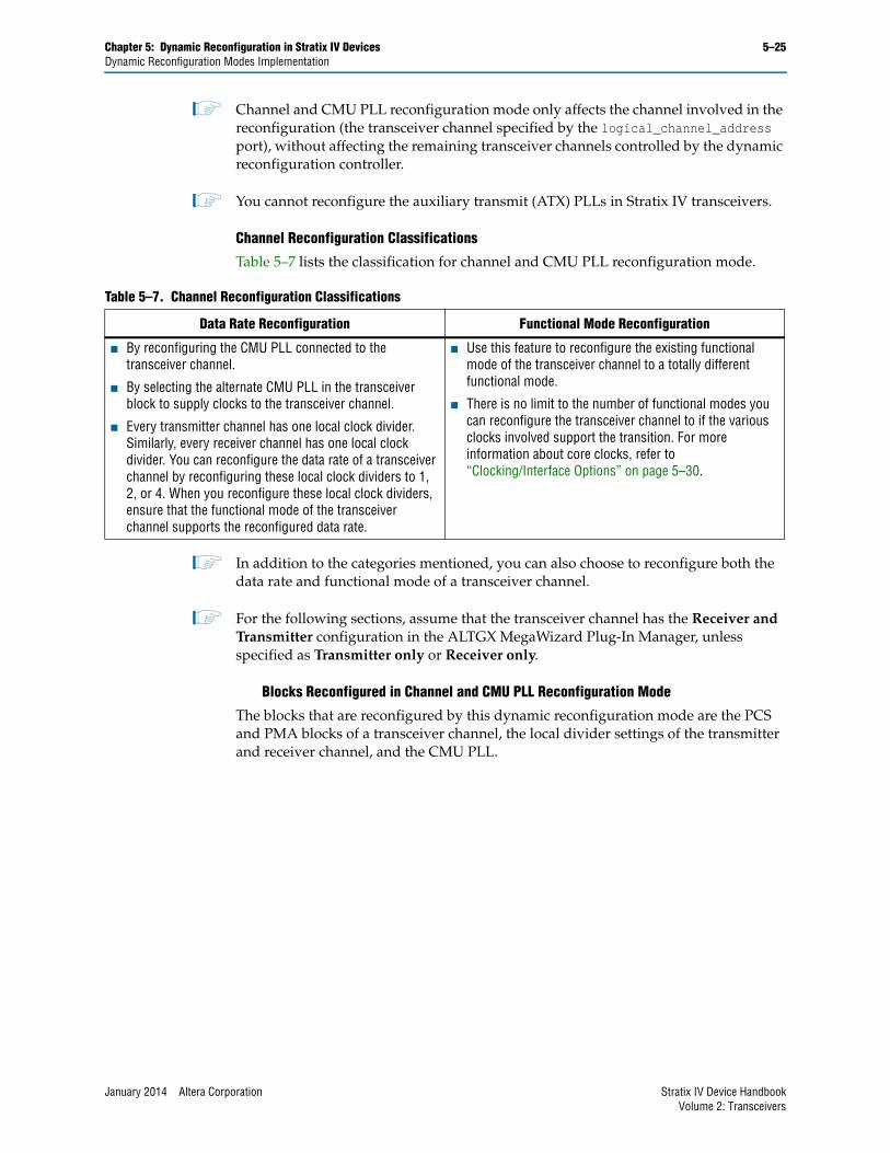
Table 5–7 lists the classification for channel and CMU PLL reconfiguration mode.
1 In addition to the categories mentioned, you can also choose to reconfigure both the data rate and functional mode of a transceiver channel.
1 For the following sections, assume that the transceiver channel has the Receiver and Transmitter configuration in the ALTGX MegaWizard Plug-In Manager, unless specified as Transmitter only or Receiver only.
Blocks Reconfigured in Channel and CMU PLL Reconfiguration Mode
The blocks that are reconfigured by this dynamic reconfiguration mode are the PCS and PMA blocks of a transceiver channel, the local divider settings of the transmitter and receiver channel, and the CMU PLL.
Table 5–7. Channel Reconfiguration Classifications
Data Rate Reconfiguration Functional Mode Reconfiguration
■ By reconfiguring the CMU PLL connected to the transceiver channel.
■ By selecting the alternate CMU PLL in the transceiver block to supply clocks to the transceiver channel.
■ Every transmitter channel has one local clock divider. Similarly, every receiver channel has one local clock divider. You can reconfigure the data rate of a transceiver channel by reconfiguring these local clock dividers to 1, 2, or 4. When you reconfigure these local clock dividers, ensure that the functional mode of the transceiver channel supports the reconfigured data rate.
■ Use this feature to reconfigure the existing functional mode of the transceiver channel to a totally different functional mode.
■ There is no limit to the number of functional modes you can reconfigure the transceiver channel to if the various clocks involved support the transition. For more information about core clocks, refer to “Clocking/Interface Options” on page 5–30.
January 2014 Altera Corporation Stratix IV Device HandbookVolume 2: Transceivers
5–26 Chapter 5: Dynamic Reconfiguration in Stratix IV DevicesDynamic Reconfiguration Modes Implementation
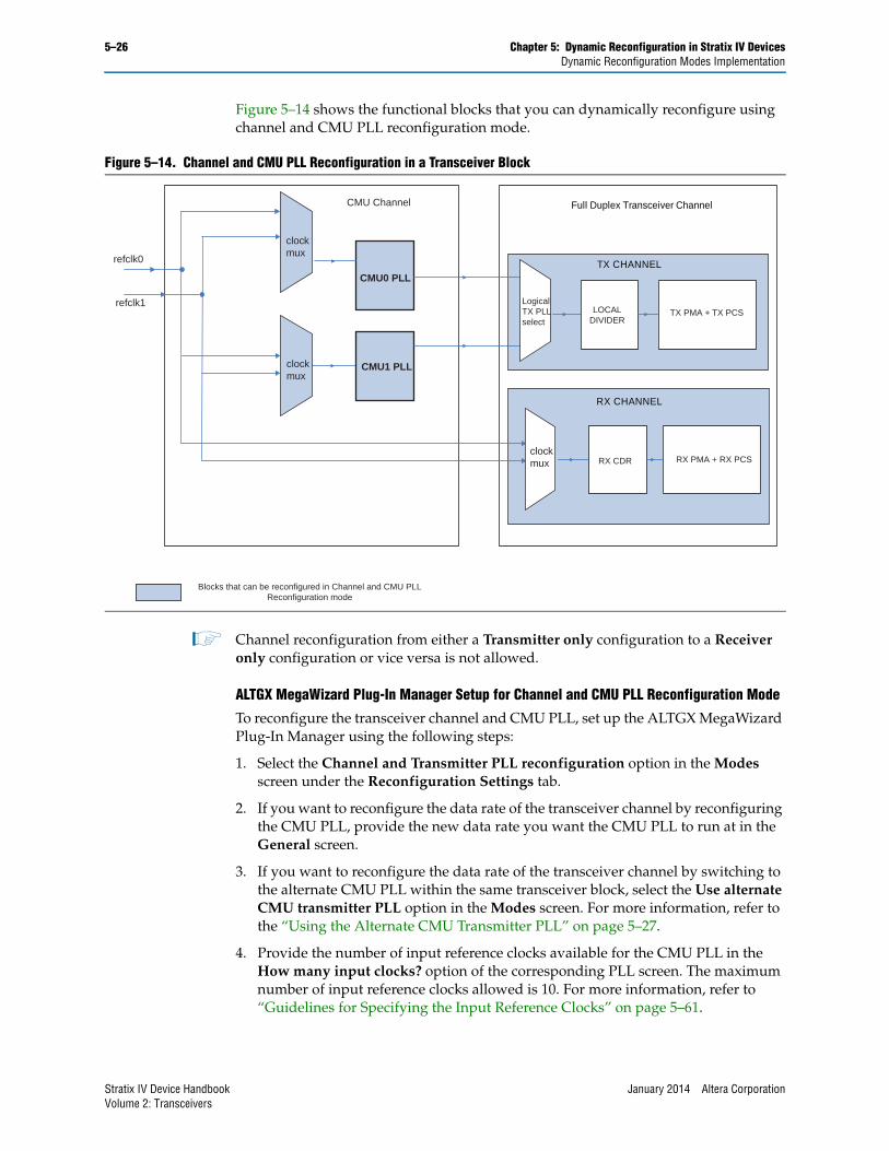
Figure 5–14 shows the functional blocks that you can dynamically reconfigure using channel and CMU PLL reconfiguration mode.
1 Channel reconfiguration from either a Transmitter only configuration to a Receiver only configuration or vice versa is not allowed.
ALTGX MegaWizard Plug-In Manager Setup for Channel and CMU PLL Reconfiguration Mode
To reconfigure the transceiver channel and CMU PLL, set up the ALTGX MegaWizard Plug-In Manager using the following steps:
1. Select the Channel and Transmitter PLL reconfiguration option in the Modes screen under the Reconfiguration Settings tab.
2. If you want to reconfigure the data rate of the transceiver channel by reconfiguring the CMU PLL, provide the new data rate you want the CMU PLL to run at in the General screen.
3. If you want to reconfigure the data rate of the transceiver channel by switching to the alternate CMU PLL within the same transceiver block, select the Use alternate CMU transmitter PLL option in the Modes screen. For more information, refer to the “Using the Alternate CMU Transmitter PLL” on page 5–27.
4. Provide the number of input reference clocks available for the CMU PLL in the How many input clocks? option of the corresponding PLL screen. The maximum number of input reference clocks allowed is 10. For more information, refer to “Guidelines for Specifying the Input Reference Clocks” on page 5–61.
Figure 5–14. Channel and CMU PLL Reconfiguration in a Transceiver Block
Full Duplex Transceiver Channel
TX CHANNEL
RX CHANNEL
refclk0
refclk1
CMU Channel
CMU0 PLL
CMU1 PLL
LOCALDIVIDER
TX PMA + TX PCS
RX PMA + RX PCSRX CDR
Blocks that can be reconfigured in Channel and CMU PLLReconfiguration mode
clockmux
LogicalTX PLLselect
clockmux
clockmux
Stratix IV Device Handbook January 2014 Altera CorporationVolume 2: Transceivers
Chapter 5: Dynamic Reconfiguration in Stratix IV Devices 5–27Dynamic Reconfiguration Modes Implementation
5. Provide the starting channel number in the Modes screen. For more information, refer to “Logical Channel Addressing” on page 5–5.
6. Provide the logical reference index of the CMU PLL in the What is the PLL logical reference index? option in the corresponding PLL screen. For more information, refer to “Selecting the Logical Reference Index of the CMU PLL” on page 5–29.
7. Provide the identification of the input reference clock used by the CMU PLL in the corresponding PLL screens.
8. Set up the Clocking/Interface options. For more information, refer to “Clocking/Interface Options” on page 5–30.
9. Set up the Channel Interface options. For more information, refer to “FPGA Fabric-Transceiver Channel Interface Selection” on page 5–36.
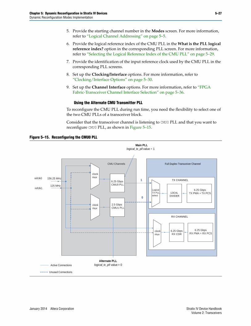
Using the Alternate CMU Transmitter PLL
To reconfigure the CMU PLL during run time, you need the flexibility to select one of the two CMU PLLs of a transceiver block.
Consider that the transceiver channel is listening to CMU0 PLL and that you want to reconfigure CMU0 PLL, as shown in Figure 5–15.
Figure 5–15. Reconfiguring the CMU0 PLL
Full Duplex Transceiver Channel
TX CHANNEL
RX CHANNEL
LOCAL DIVIDER
Active Connections
Main PLLlogical_tx_pll value = 1
Alternate PLLlogical_tx_pll value = 0
1
0
Unused Connections
CMU Channels
refclk0
refclk1
156.25 MHz
125 MHz
6.25 GbpsCMU0 PLL
2.5 GbpsCMU1 PLL
LogicalTX PLLselect
clockmux
6.25 GbpsRX CDR
6.25 GbpsTX PMA + TX PCS
6.25 GbpsRX PMA + RX PCS
clockmux
clockmux
January 2014 Altera Corporation Stratix IV Device HandbookVolume 2: Transceivers
5–28 Chapter 5: Dynamic Reconfiguration in Stratix IV DevicesDynamic Reconfiguration Modes Implementation
You can select CMU0 PLL by specifying its identity in the ALTGX MegaWizard Plug-In Manager. This identification is referred to as the logical tx pll value. This value provides a logical identification to CMU0 PLL and associates it with a transceiver channel without requiring the knowledge of its physical location.
In the ALTGX MegaWizard Plug-In Manager, the transmitter PLL configuration set in the General screen is called the main PLL. When you provide the alternate PLL with a logical tx pll value (for example, 0), the main PLL automatically takes the complement value 1. The logical tx pll value for the main PLL is stored along with the other transceiver channel information in the generated .mif.
1 The main PLL corresponds to the CMU PLL configuration set in the General screen of the ALTGX MegaWizard Plug-In Manager. The alternate PLL corresponds to the CMU PLL configuration set in the Alt PLL screen.
Stratix IV Device Handbook January 2014 Altera CorporationVolume 2: Transceivers
Chapter 5: Dynamic Reconfiguration in Stratix IV Devices 5–29Dynamic Reconfiguration Modes Implementation
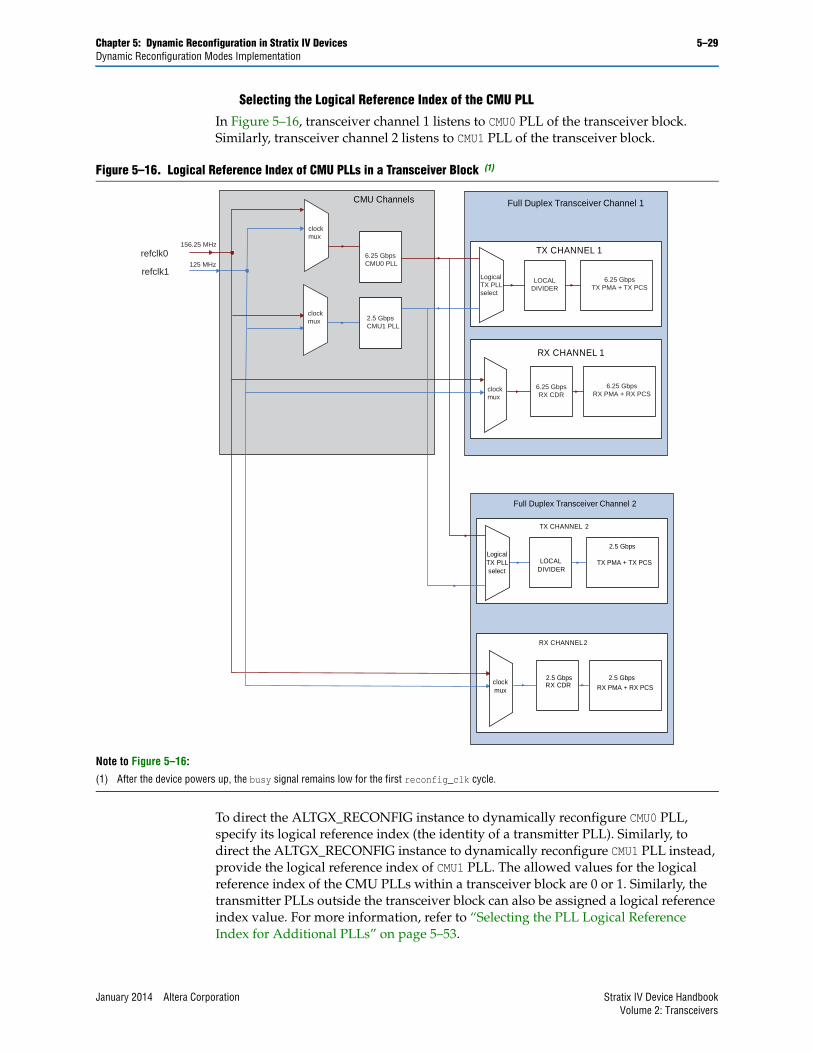
Selecting the Logical Reference Index of the CMU PLL
In Figure 5–16, transceiver channel 1 listens to CMU0 PLL of the transceiver block. Similarly, transceiver channel 2 listens to CMU1 PLL of the transceiver block.
To direct the ALTGX_RECONFIG instance to dynamically reconfigure CMU0 PLL, specify its logical reference index (the identity of a transmitter PLL). Similarly, to direct the ALTGX_RECONFIG instance to dynamically reconfigure CMU1 PLL instead, provide the logical reference index of CMU1 PLL. The allowed values for the logical reference index of the CMU PLLs within a transceiver block are 0 or 1. Similarly, the transmitter PLLs outside the transceiver block can also be assigned a logical reference index value. For more information, refer to “Selecting the PLL Logical Reference Index for Additional PLLs” on page 5–53.
Figure 5–16. Logical Reference Index of CMU PLLs in a Transceiver Block (1)
Note to Figure 5–16:
(1) After the device powers up, the busy signal remains low for the first reconfig_clk cycle.
Full Duplex Transceiver Channel 1
TX CHANNEL 1
CMU Channels
Full Duplex Transceiver Channel 2
RX CDR
TX PMA + TX PCS
TX CHANNEL 2
Logical TX PLL select
RX CHANNEL 2
2.5 Gbps
2.5 Gbps 2.5 Gbps
LOCAL DIVIDER
clock mux
refclk0
refclk1
156.25 MHz
125 MHz6.25 GbpsCMU0 PLL
2.5 GbpsCMU1 PLL
RX CHANNEL 1
LogicalTX PLLselect
clockmux
6.25 GbpsRX CDR
6.25 GbpsRX PMA + RX PCS
6.25 GbpsTX PMA + TX PCS
LOCALDIVIDER
clockmux
clockmux
RX PMA + RX PCS
January 2014 Altera Corporation Stratix IV Device HandbookVolume 2: Transceivers
5–30 Chapter 5: Dynamic Reconfiguration in Stratix IV DevicesDynamic Reconfiguration Modes Implementation
1 The logical reference index of the CMU0 PLL within a transceiver block is always the complement of the logical reference index of the CMU1 PLL within the same transceiver block.
1 This logical reference index value is stored as logical tx pll, along with the other transceiver channel settings in the .mif.
Clocking/Interface Options
The following describes the Clocking/Interface options. The core clocking setup describes the transceiver core clocks that are the write and read clocks of the transmit (TX) phase compensation FIFO and the receive (RX) phase compensation FIFO, respectively. Core clocking is classified as transmitter core clocking and receiver core clocking.
Transmitter core clocking refers to the clock that is used to write the parallel data from the FPGA fabric into the Transmit Phase Compensation FIFO. You can use one of the following clocks to write into the Transmit Phase Compensation FIFO:
■ tx_coreclk—You can use a clock of the same frequency as tx_clkout from the FPGA fabric to provide the write clock to the Transmit Phase Compensation FIFO. If you use tx_coreclk, it overrides the tx_clkout options in the ALTGX MegaWizard Plug-In Manager.
■ tx_clkout—The Quartus II software automatically routes tx_clkout to the FPGA fabric and back into the TX phase compensation FIFO.
1 The Clocking/Interface screen is not available for PMA-only channels.
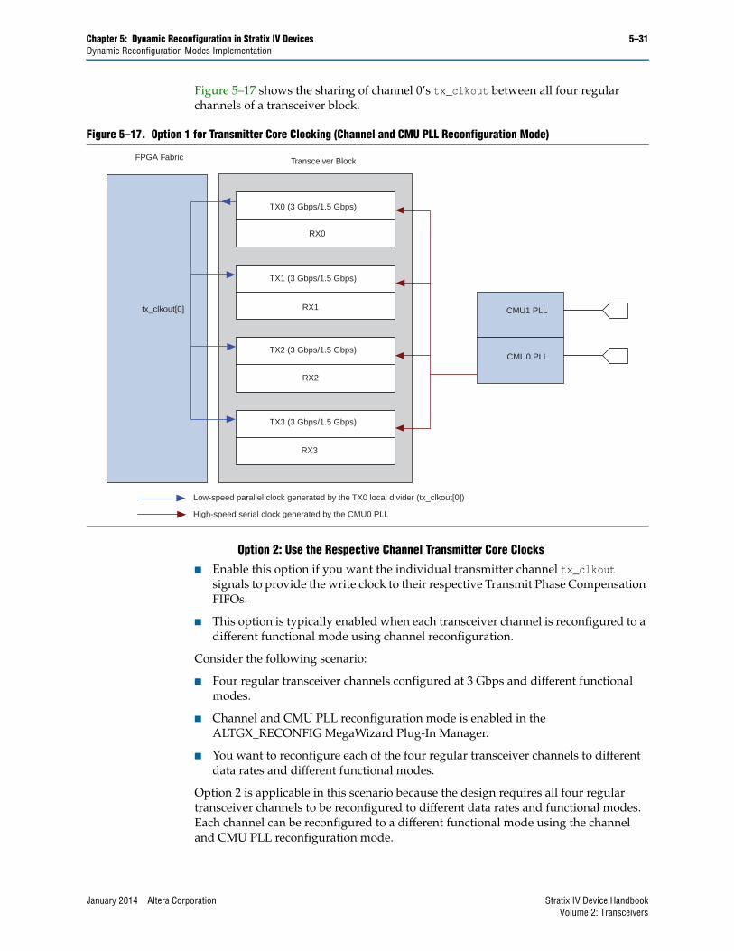
Option 1: Share a Single Transmitter Core Clock Between Transmitters
■ Enable this option if you want tx_clkout of the first channel (channel 0) of the transceiver block to provide the write clock to the TX phase compensation FIFOs of the remaining channels in the transceiver block.
■ This option is typically enabled when all the channels of a transceiver block are of the same functional mode and data rate, and are reconfigured to the identical functional mode and data rate.
Consider the following scenario:
■ Four regular transceiver channels configured at 3 Gbps and in the same functional mode.
■ Channel and CMU PLL reconfiguration mode is enabled in the ALTGX_RECONFIG MegaWizard Plug-In Manager.
■ You want to reconfigure all four regular transceiver channels to 1.5 Gbps and vice versa.
Option 1 is applicable in this scenario because it saves clock resources.
Stratix IV Device Handbook January 2014 Altera CorporationVolume 2: Transceivers
Chapter 5: Dynamic Reconfiguration in Stratix IV Devices 5–31Dynamic Reconfiguration Modes Implementation
Figure 5–17 shows the sharing of channel 0’s tx_clkout between all four regular channels of a transceiver block.
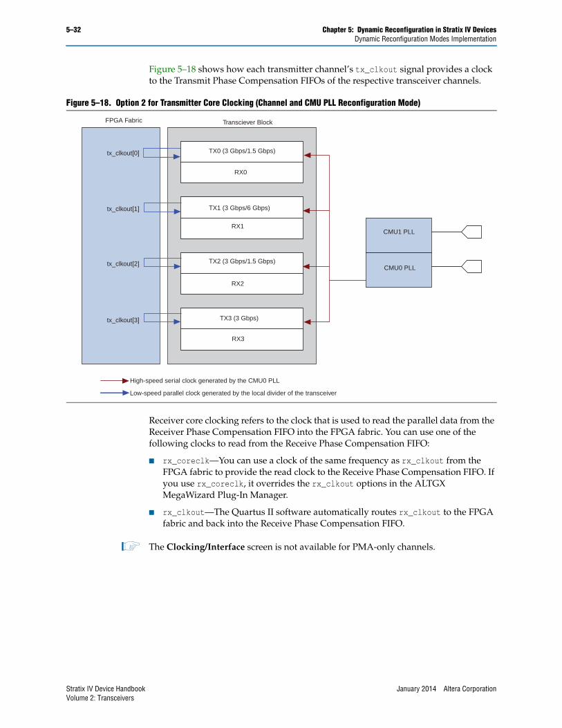
Option 2: Use the Respective Channel Transmitter Core Clocks
■ Enable this option if you want the individual transmitter channel tx_clkout signals to provide the write clock to their respective Transmit Phase Compensation FIFOs.
■ This option is typically enabled when each transceiver channel is reconfigured to a different functional mode using channel reconfiguration.
Consider the following scenario:
■ Four regular transceiver channels configured at 3 Gbps and different functional modes.
■ Channel and CMU PLL reconfiguration mode is enabled in the ALTGX_RECONFIG MegaWizard Plug-In Manager.
■ You want to reconfigure each of the four regular transceiver channels to different data rates and different functional modes.
Option 2 is applicable in this scenario because the design requires all four regular transceiver channels to be reconfigured to different data rates and functional modes. Each channel can be reconfigured to a different functional mode using the channel and CMU PLL reconfiguration mode.
Figure 5–17. Option 1 for Transmitter Core Clocking (Channel and CMU PLL Reconfiguration Mode)
TX0 (3 Gbps/1.5 Gbps)
TX1 (3 Gbps/1.5 Gbps)
TX2 (3 Gbps/1.5 Gbps)
TX3 (3 Gbps/1.5 Gbps)
RX3
RX2
RX1
RX0
CMU1 PLL
CMU0 PLL
FPGA Fabric Transceiver Block
tx_clkout[0]
Low-speed parallel clock generated by the TX0 local divider (tx_clkout[0])
High-speed serial clock generated by the CMU0 PLL
January 2014 Altera Corporation Stratix IV Device HandbookVolume 2: Transceivers
5–32 Chapter 5: Dynamic Reconfiguration in Stratix IV DevicesDynamic Reconfiguration Modes Implementation
Figure 5–18 shows how each transmitter channel’s tx_clkout signal provides a clock to the Transmit Phase Compensation FIFOs of the respective transceiver channels.
Receiver core clocking refers to the clock that is used to read the parallel data from the Receiver Phase Compensation FIFO into the FPGA fabric. You can use one of the following clocks to read from the Receive Phase Compensation FIFO:
■ rx_coreclk—You can use a clock of the same frequency as rx_clkout from the FPGA fabric to provide the read clock to the Receive Phase Compensation FIFO. If you use rx_coreclk, it overrides the rx_clkout options in the ALTGX MegaWizard Plug-In Manager.
■ rx_clkout—The Quartus II software automatically routes rx_clkout to the FPGA fabric and back into the Receive Phase Compensation FIFO.
1 The Clocking/Interface screen is not available for PMA-only channels.
Figure 5–18. Option 2 for Transmitter Core Clocking (Channel and CMU PLL Reconfiguration Mode)
TX0 (3 Gbps/1.5 Gbps)
TX1 (3 Gbps/6 Gbps)
TX2 (3 Gbps/1.5 Gbps)
TX3 (3 Gbps)
RX0
RX1
RX2
RX3
CMU1 PLL
CMU0 PLL
FPGA Fabric Transciever Block
High-speed serial clock generated by the CMU0 PLL
tx_clkout[0]
tx_clkout[1]
tx_clkout[2]
tx_clkout[3]
Low-speed parallel clock generated by the local divider of the transceiver
Stratix IV Device Handbook January 2014 Altera CorporationVolume 2: Transceivers
Chapter 5: Dynamic Reconfiguration in Stratix IV Devices 5–33Dynamic Reconfiguration Modes Implementation
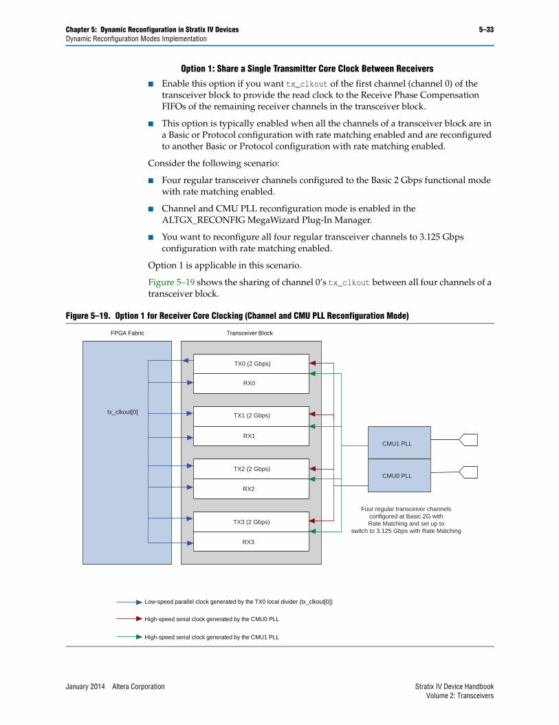
Option 1: Share a Single Transmitter Core Clock Between Receivers
■ Enable this option if you want tx_clkout of the first channel (channel 0) of the transceiver block to provide the read clock to the Receive Phase Compensation FIFOs of the remaining receiver channels in the transceiver block.
■ This option is typically enabled when all the channels of a transceiver block are in a Basic or Protocol configuration with rate matching enabled and are reconfigured to another Basic or Protocol configuration with rate matching enabled.
Consider the following scenario:
■ Four regular transceiver channels configured to the Basic 2 Gbps functional mode with rate matching enabled.
■ Channel and CMU PLL reconfiguration mode is enabled in the ALTGX_RECONFIG MegaWizard Plug-In Manager.
■ You want to reconfigure all four regular transceiver channels to 3.125 Gbps configuration with rate matching enabled.
Option 1 is applicable in this scenario.
Figure 5–19 shows the sharing of channel 0’s tx_clkout between all four channels of a transceiver block.
Figure 5–19. Option 1 for Receiver Core Clocking (Channel and CMU PLL Reconfiguration Mode)
High-speed serial clock generated by the CMU0 PLL
Low-speed parallel clock generated by the TX0 local divider (tx_clkout[0])
High-speed serial clock generated by the CMU1 PLL
FPGA Fabric Transceiver Block
tx_clkout[0]
TX0 (2 Gbps)
RX0
TX1 (2 Gbps)
TX2 (2 Gbps)
TX3 (2 Gbps)
RX1
RX2
RX3
CMU1 PLL
CMU0 PLL
Four regular transceiver channelsconfigured at Basic 2G withRate Matching and set up to
switch to 3.125 Gbps with Rate Matching
January 2014 Altera Corporation Stratix IV Device HandbookVolume 2: Transceivers
5–34 Chapter 5: Dynamic Reconfiguration in Stratix IV DevicesDynamic Reconfiguration Modes Implementation
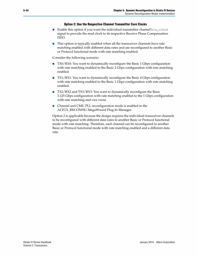
Option 2: Use the Respective Channel Transmitter Core Clocks
■ Enable this option if you want the individual transmitter channel’s tx_clkout signal to provide the read clock to its respective Receive Phase Compensation FIFO.
■ This option is typically enabled when all the transceiver channels have rate matching enabled with different data rates and are reconfigured to another Basic or Protocol functional mode with rate matching enabled.
Consider the following scenario:
■ TX0/RX0: You want to dynamically reconfigure the Basic 1 Gbps configuration with rate matching enabled to the Basic 2 Gbps configuration with rate matching enabled.
■ TX1/RX1: You want to dynamically reconfigure the Basic 4 Gbps configuration with rate matching enabled to the Basic 1 Gbps configuration with rate matching enabled.
■ TX2/RX2 and TX3/RX3: You want to dynamically reconfigure the Basic 3.125 Gbps configuration with rate matching enabled to the 1 Gbps configuration with rate matching and vice versa.
■ Channel and CMU PLL reconfiguration mode is enabled in the ALTGX_RECONFIG MegaWizard Plug-In Manager.
Option 2 is applicable because the design requires the individual transceiver channels to be reconfigured with different data rates to another Basic or Protocol functional mode with rate matching. Therefore, each channel can be reconfigured to another Basic or Protocol functional mode with rate matching enabled and a different data rate.
Stratix IV Device Handbook January 2014 Altera CorporationVolume 2: Transceivers
Chapter 5: Dynamic Reconfiguration in Stratix IV Devices 5–35Dynamic Reconfiguration Modes Implementation
Figure 5–20 shows the respective tx_clkout of each channel clocking the respective channels of a transceiver block.
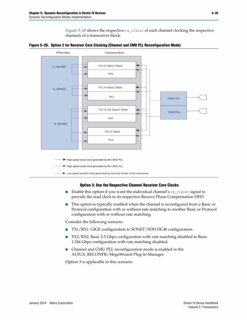
Option 3: Use the Respective Channel Receiver Core Clocks
■ Enable this option if you want the individual channel’s rx_clkout signal to provide the read clock to its respective Receive Phase Compensation FIFO.
■ This option is typically enabled when the channel is reconfigured from a Basic or Protocol configuration with or without rate matching to another Basic or Protocol configuration with or without rate matching.
Consider the following scenario:
■ TX1/RX1: GIGE configuration to SONET/SDH OC48 configuration.
■ TX2/RX2: Basic 2.5 Gbps configuration with rate matching disabled to Basic 1.244 Gbps configuration with rate matching disabled.
■ Channel and CMU PLL reconfiguration mode is enabled in the ALTGX_RECONFIG MegaWizard Plug-In Manager.
Option 3 is applicable in this scenario.
Figure 5–20. Option 2 for Receiver Core Clocking (Channel and CMU PLL Reconfiguration Mode)
High-speed serial clock generated by the CMU0 PLL
High-speed serial clock generated by the CMU1 PLL
FPGA Fabric Transceiver Block
tx_clkout[0]
tx_clkout[1]
tx_clkout[2]
RX0
RX1
RX2
RX3
TX0 (2 Gbps/1 Gbps)
TX1 (4 Gbps/1 Gbps)
TX2 (3.125 Gbps/1 Gbps)
TX3 (2 Gbps)
CMU1 PLL
CMU0 PLL
Low-speed parallel clock generated by the local divider of the transceiver
January 2014 Altera Corporation Stratix IV Device HandbookVolume 2: Transceivers
5–36 Chapter 5: Dynamic Reconfiguration in Stratix IV DevicesDynamic Reconfiguration Modes Implementation
Figure 5–21 shows the respective rx_clkout of each channel clocking the respective receiver channels of a transceiver block.
FPGA Fabric-Transceiver Channel Interface Selection
This section describes the ALTGX MegaWizard Plug-In Manager settings related to the FPGA fabric-transceiver channel interface data width when you select and activate channel and CMU PLL reconfiguration mode. You must set up the FPGA fabric-transceiver channel interface data width when functional mode reconfiguration involves:
■ changes in the FPGA fabric-transceiver channel data width
OR
■ enables and disables the static PCS blocks of the transceiver channel
You can set up the FPGA fabric-transceiver channel interface data width by enabling the Channel Interface option in the Modes screen.
Enable the Channel Interface option if the reconfiguration channel has:
■ changed the FPGA fabric-transceiver channel interface data width
OR
■ changed the input control signals and output status signals
Figure 5–21. Option 3 for Receiver Core Clocking (Channel and CMU PLL Reconfiguration Mode)
High-speed serial clock generated by the CMU0 PLL
High-speed serial clock generated by the CMU1 PLL
FPGA Fabric Transceiver Block
rx_clkout[0]
rx_clkout[1] RX1
RX0
TX0 (2 Gbps)
TX1 (2 Gbps)
CMU1 PLL
CMU0 PLL
Low-speed parallel clock generated by the local divider of the transceiver
Stratix IV Device Handbook January 2014 Altera CorporationVolume 2: Transceivers
Chapter 5: Dynamic Reconfiguration in Stratix IV Devices 5–37Dynamic Reconfiguration Modes Implementation
There are two signals available when you enable the Channel Interface option:
■ tx_datainfull—The width of this input signal depends on the number of channels you set up in the General screen. It is 44 bits wide per channel. This signal is available only for Transmitter only and Receiver and Transmitter configurations. This port replaces the existing tx_datain port.
■ rx_dataoutfull—The width of this output signal depends on the number of channels you set up in the General screen. It is 64 bits wide per channel. This signal is available only for Receiver only and Receiver and Transmitter configurations. This port replaces the existing rx_dataout port.
1 In addition to these two ports, you can select the necessary control and status signals for the reconfigured channel in the Clocking/Interface screen.
f For more information about control and status signals, refer to the “Transceiver Port Lists” section in the Transceiver Architecture in Stratix IV Devices chapter.
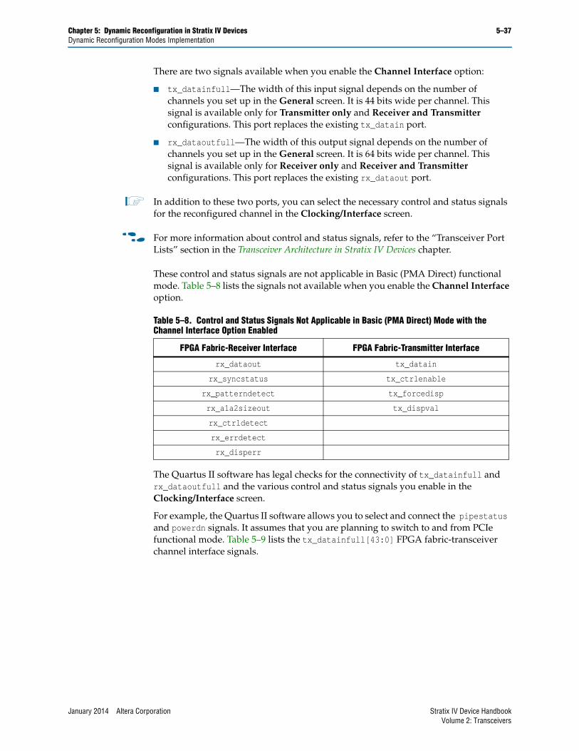
These control and status signals are not applicable in Basic (PMA Direct) functional mode. Table 5–8 lists the signals not available when you enable the Channel Interface option.
The Quartus II software has legal checks for the connectivity of tx_datainfull and rx_dataoutfull and the various control and status signals you enable in the Clocking/Interface screen.
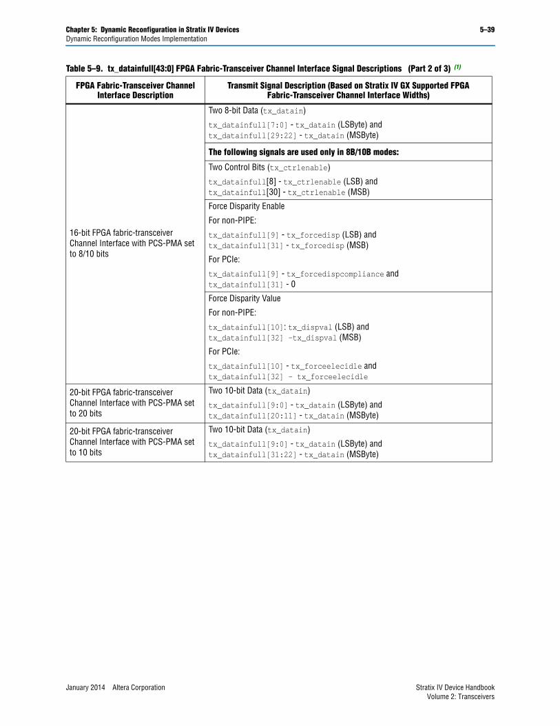
For example, the Quartus II software allows you to select and connect the pipestatus and powerdn signals. It assumes that you are planning to switch to and from PCIe functional mode. Table 5–9 lists the tx_datainfull[43:0] FPGA fabric-transceiver channel interface signals.
Table 5–8. Control and Status Signals Not Applicable in Basic (PMA Direct) Mode with the Channel Interface Option Enabled
FPGA Fabric-Receiver Interface FPGA Fabric-Transmitter Interface
rx_dataout tx_datain
rx_syncstatus tx_ctrlenable
rx_patterndetect tx_forcedisp
rx_a1a2sizeout tx_dispval
rx_ctrldetect
rx_errdetect
rx_disperr
January 2014 Altera Corporation Stratix IV Device HandbookVolume 2: Transceivers
5–38 Chapter 5: Dynamic Reconfiguration in Stratix IV DevicesDynamic Reconfiguration Modes Implementation
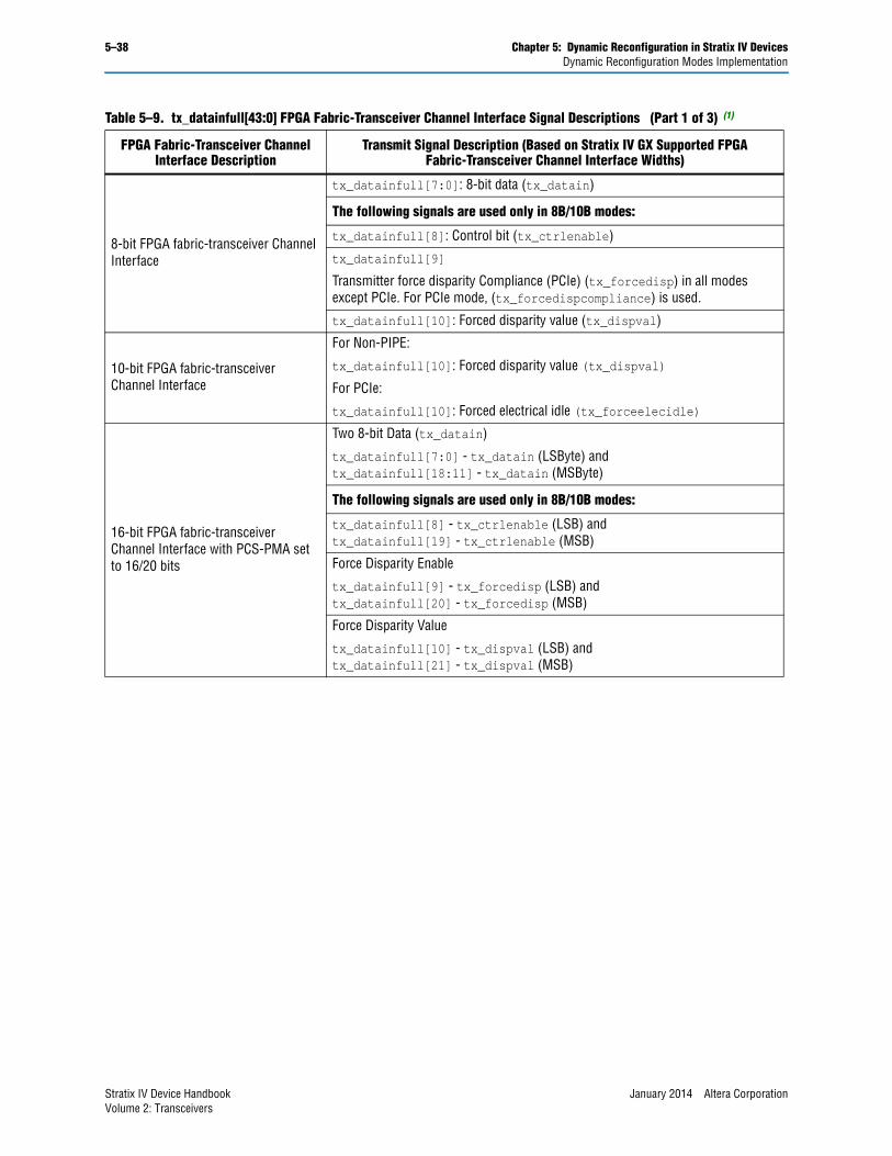
Table 5–9. tx_datainfull[43:0] FPGA Fabric-Transceiver Channel Interface Signal Descriptions (Part 1 of 3) (1)
FPGA Fabric-Transceiver Channel Interface Description
Transmit Signal Description (Based on Stratix IV GX Supported FPGA Fabric-Transceiver Channel Interface Widths)
8-bit FPGA fabric-transceiver Channel Interface
tx_datainfull[7:0]: 8-bit data (tx_datain)
The following signals are used only in 8B/10B modes:
tx_datainfull[8]: Control bit (tx_ctrlenable)
tx_datainfull[9]
Transmitter force disparity Compliance (PCIe) (tx_forcedisp) in all modes except PCIe. For PCIe mode, (tx_forcedispcompliance) is used.
tx_datainfull[10]: Forced disparity value (tx_dispval)
10-bit FPGA fabric-transceiver Channel Interface
For Non-PIPE:
tx_datainfull[10]: Forced disparity value (tx_dispval)
For PCIe:
tx_datainfull[10]: Forced electrical idle (tx_forceelecidle)
16-bit FPGA fabric-transceiver Channel Interface with PCS-PMA set to 16/20 bits
Two 8-bit Data (tx_datain)
tx_datainfull[7:0] - tx_datain (LSByte) andtx_datainfull[18:11] - tx_datain (MSByte)
The following signals are used only in 8B/10B modes:
tx_datainfull[8] - tx_ctrlenable (LSB) andtx_datainfull[19] - tx_ctrlenable (MSB)
Force Disparity Enable
tx_datainfull[9] - tx_forcedisp (LSB) andtx_datainfull[20] - tx_forcedisp (MSB)
Force Disparity Value
tx_datainfull[10] - tx_dispval (LSB) andtx_datainfull[21] - tx_dispval (MSB)
Stratix IV Device Handbook January 2014 Altera CorporationVolume 2: Transceivers
Chapter 5: Dynamic Reconfiguration in Stratix IV Devices 5–39Dynamic Reconfiguration Modes Implementation
16-bit FPGA fabric-transceiver Channel Interface with PCS-PMA set to 8/10 bits
Two 8-bit Data (tx_datain)
tx_datainfull[7:0] - tx_datain (LSByte) andtx_datainfull[29:22] - tx_datain (MSByte)
The following signals are used only in 8B/10B modes:
Two Control Bits (tx_ctrlenable)
tx_datainfull[8] - tx_ctrlenable (LSB) andtx_datainfull[30] - tx_ctrlenable (MSB)
Force Disparity Enable
For non-PIPE:
tx_datainfull[9] - tx_forcedisp (LSB) andtx_datainfull[31] - tx_forcedisp (MSB)
For PCIe:
tx_datainfull[9] - tx_forcedispcompliance andtx_datainfull[31] - 0
Force Disparity Value
For non-PIPE:
tx_datainfull[10]: tx_dispval (LSB) and tx_datainfull[32] -tx_dispval (MSB)
For PCIe:
tx_datainfull[10] - tx_forceelecidle and tx_datainfull[32] - tx_forceelecidle
20-bit FPGA fabric-transceiver Channel Interface with PCS-PMA set to 20 bits
Two 10-bit Data (tx_datain)
tx_datainfull[9:0] - tx_datain (LSByte) and tx_datainfull[20:11] - tx_datain (MSByte)
20-bit FPGA fabric-transceiver Channel Interface with PCS-PMA set to 10 bits
Two 10-bit Data (tx_datain)
tx_datainfull[9:0] - tx_datain (LSByte) and tx_datainfull[31:22] - tx_datain (MSByte)
Table 5–9. tx_datainfull[43:0] FPGA Fabric-Transceiver Channel Interface Signal Descriptions (Part 2 of 3) (1)
FPGA Fabric-Transceiver Channel Interface Description
Transmit Signal Description (Based on Stratix IV GX Supported FPGA Fabric-Transceiver Channel Interface Widths)
January 2014 Altera Corporation Stratix IV Device HandbookVolume 2: Transceivers
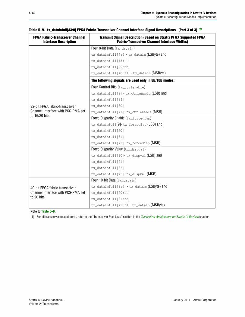
5–40 Chapter 5: Dynamic Reconfiguration in Stratix IV DevicesDynamic Reconfiguration Modes Implementation
32-bit FPGA fabric-transceiver Channel Interface with PCS-PMA set to 16/20 bits
Four 8-bit Data (tx_datain)
tx_datainfull[7:0]- tx_datain (LSByte) and
tx_datainfull[18:11]
tx_datainfull[29:22]
tx_datainfull[40:33] - tx_datain (MSByte)
The following signals are used only in 8B/10B modes:
Four Control Bits (tx_ctrlenable)
tx_datainfull[8] - tx_ctrlenable (LSB) and
tx_datainfull[19]
tx_datainfull[30]
tx_datainfull[41]- tx_ctrlenable (MSB)
Force Disparity Enable (tx_forcedisp)
tx_datainfull[9]- tx_forcedisp (LSB) and
tx_datainfull[20]
tx_datainfull[31]
tx_datainfull[42]- tx_forcedisp (MSB)
Force Disparity Value (tx_dispval)
tx_datainfull[10]- tx_dispval (LSB) and
tx_datainfull[21]
tx_datainfull[32]
tx_datainfull[43]- tx_dispval (MSB)
40-bit FPGA fabric-transceiver Channel Interface with PCS-PMA set to 20 bits
Four 10-bit Data (tx_datain)
tx_datainfull[9:0] - tx_datain (LSByte) and
tx_datainfull[20:11]
tx_datainfull[31:22]
tx_datainfull[42:33]- tx_datain (MSByte)
Note to Table 5–9:
(1) For all transceiver-related ports, refer to the “Transceiver Port Lists” section in the Transceiver Architecture for Stratix IV Devices chapter.
Table 5–9. tx_datainfull[43:0] FPGA Fabric-Transceiver Channel Interface Signal Descriptions (Part 3 of 3) (1)
FPGA Fabric-Transceiver Channel Interface Description
Transmit Signal Description (Based on Stratix IV GX Supported FPGA Fabric-Transceiver Channel Interface Widths)
Stratix IV Device Handbook January 2014 Altera CorporationVolume 2: Transceivers
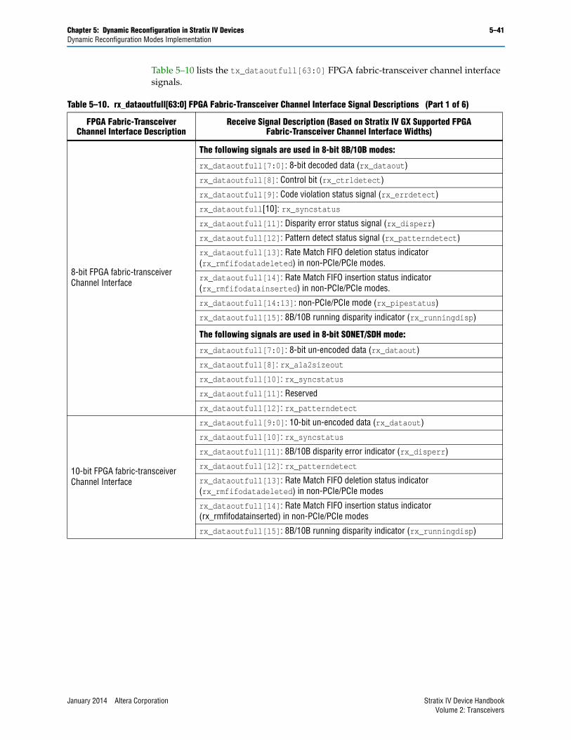
Chapter 5: Dynamic Reconfiguration in Stratix IV Devices 5–41Dynamic Reconfiguration Modes Implementation
Table 5–10 lists the tx_dataoutfull[63:0] FPGA fabric-transceiver channel interface signals.
Table 5–10. rx_dataoutfull[63:0] FPGA Fabric-Transceiver Channel Interface Signal Descriptions (Part 1 of 6)
FPGA Fabric-Transceiver Channel Interface Description
Receive Signal Description (Based on Stratix IV GX Supported FPGA Fabric-Transceiver Channel Interface Widths)
8-bit FPGA fabric-transceiver Channel Interface
The following signals are used in 8-bit 8B/10B modes:
rx_dataoutfull[7:0]: 8-bit decoded data (rx_dataout)
rx_dataoutfull[8]: Control bit (rx_ctrldetect)
rx_dataoutfull[9]: Code violation status signal (rx_errdetect)
rx_dataoutfull[10]: rx_syncstatus
rx_dataoutfull[11]: Disparity error status signal (rx_disperr)
rx_dataoutfull[12]: Pattern detect status signal (rx_patterndetect)
rx_dataoutfull[13]: Rate Match FIFO deletion status indicator (rx_rmfifodatadeleted) in non-PCIe/PCIe modes.
rx_dataoutfull[14]: Rate Match FIFO insertion status indicator (rx_rmfifodatainserted) in non-PCIe/PCIe modes.
rx_dataoutfull[14:13]: non-PCIe/PCIe mode (rx_pipestatus)
rx_dataoutfull[15]: 8B/10B running disparity indicator (rx_runningdisp)
The following signals are used in 8-bit SONET/SDH mode:
rx_dataoutfull[7:0]: 8-bit un-encoded data (rx_dataout)
rx_dataoutfull[8]: rx_a1a2sizeout
rx_dataoutfull[10]: rx_syncstatus
rx_dataoutfull[11]: Reserved
rx_dataoutfull[12]: rx_patterndetect
10-bit FPGA fabric-transceiver Channel Interface
rx_dataoutfull[9:0]: 10-bit un-encoded data (rx_dataout)
rx_dataoutfull[10]: rx_syncstatus
rx_dataoutfull[11]: 8B/10B disparity error indicator (rx_disperr)
rx_dataoutfull[12]: rx_patterndetect
rx_dataoutfull[13]: Rate Match FIFO deletion status indicator (rx_rmfifodatadeleted) in non-PCIe/PCIe modes
rx_dataoutfull[14]: Rate Match FIFO insertion status indicator (rx_rmfifodatainserted) in non-PCIe/PCIe modes
rx_dataoutfull[15]: 8B/10B running disparity indicator (rx_runningdisp)
January 2014 Altera Corporation Stratix IV Device HandbookVolume 2: Transceivers
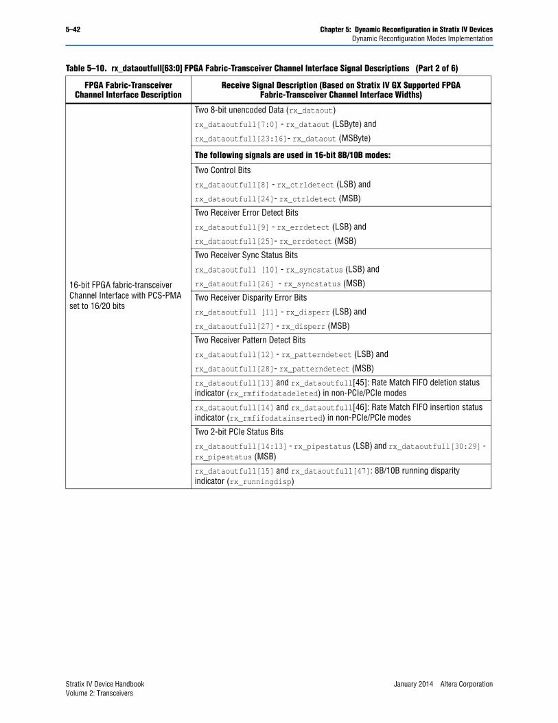
5–42 Chapter 5: Dynamic Reconfiguration in Stratix IV DevicesDynamic Reconfiguration Modes Implementation
16-bit FPGA fabric-transceiver Channel Interface with PCS-PMA set to 16/20 bits
Two 8-bit unencoded Data (rx_dataout)
rx_dataoutfull[7:0] - rx_dataout (LSByte) and
rx_dataoutfull[23:16]- rx_dataout (MSByte)
The following signals are used in 16-bit 8B/10B modes:
Two Control Bits
rx_dataoutfull[8] - rx_ctrldetect (LSB) and
rx_dataoutfull[24]- rx_ctrldetect (MSB)
Two Receiver Error Detect Bits
rx_dataoutfull[9] - rx_errdetect (LSB) and
rx_dataoutfull[25]- rx_errdetect (MSB)
Two Receiver Sync Status Bits
rx_dataoutfull [10] - rx_syncstatus (LSB) and
rx_dataoutfull[26] - rx_syncstatus (MSB)
Two Receiver Disparity Error Bits
rx_dataoutfull [11] - rx_disperr (LSB) and
rx_dataoutfull[27] - rx_disperr (MSB)
Two Receiver Pattern Detect Bits
rx_dataoutfull[12] - rx_patterndetect (LSB) and
rx_dataoutfull[28]- rx_patterndetect (MSB)
rx_dataoutfull[13] and rx_dataoutfull[45]: Rate Match FIFO deletion status indicator (rx_rmfifodatadeleted) in non-PCIe/PCIe modes
rx_dataoutfull[14] and rx_dataoutfull[46]: Rate Match FIFO insertion status indicator (rx_rmfifodatainserted) in non-PCIe/PCIe modes
Two 2-bit PCIe Status Bits
rx_dataoutfull[14:13] - rx_pipestatus (LSB) and rx_dataoutfull[30:29] - rx_pipestatus (MSB)
rx_dataoutfull[15] and rx_dataoutfull[47]: 8B/10B running disparity indicator (rx_runningdisp)
Table 5–10. rx_dataoutfull[63:0] FPGA Fabric-Transceiver Channel Interface Signal Descriptions (Part 2 of 6)
FPGA Fabric-Transceiver Channel Interface Description
Receive Signal Description (Based on Stratix IV GX Supported FPGA Fabric-Transceiver Channel Interface Widths)
Stratix IV Device Handbook January 2014 Altera CorporationVolume 2: Transceivers
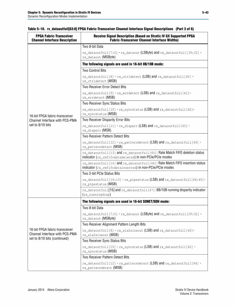
Chapter 5: Dynamic Reconfiguration in Stratix IV Devices 5–43Dynamic Reconfiguration Modes Implementation
16-bit FPGA fabric-transceiver Channel Interface with PCS-PMA set to 8/10 bits
Two 8-bit Data
rx_dataoutfull[7:0] - rx_dataout (LSByte) and rx_dataoutfull[39:32] - rx_dataout (MSByte)
The following signals are used in 16-bit 8B/10B mode:
Two Control Bits
rx_dataoutfull[8] - rx_ctrldetect (LSB) and rx_dataoutfull[40] - rx_ctrldetect (MSB)
Two Receiver Error Detect Bits
rx_dataoutfull[9] - rx_errdetect (LSB) and rx_dataoutfull[41]- rx_errdetect (MSB)
Two Receiver Sync Status Bits
rx_dataoutfull[10] - rx_syncstatus (LSB) and rx_dataoutfull[42]- rx_syncstatus (MSB)
Two Receiver Disparity Error Bits
rx_dataoutfull[11] - rx_disperr (LSB) and rx_dataoutfull[43] - rx_disperr (MSB)
Two Receiver Pattern Detect Bits
rx_dataoutfull[12] - rx_patterndetect (LSB) and rx_dataoutfull[44] - rx_patterndetect (MSB)
rx_dataoutfull[13] and rx_dataoutfull[45]: Rate Match FIFO deletion status indicator (rx_rmfifodatadeleted) in non-PCIe/PCIe modes
rx_dataoutfull[14] and rx_dataoutfull[46]: Rate Match FIFO insertion status indicator (rx_rmfifodatainserted) in non-PCIe/PCIe modes
Two 2-bit PCIe Status Bits
rx_dataoutfull[14:13] - rx_pipestatus (LSB) and rx_dataoutfull[46:45]- rx_pipestatus (MSB)
rx_dataoutfull[15] and rx_dataoutfull[47]: 8B/10B running disparity indicator (rx_runningdisp)
16-bit FPGA fabric-transceiver Channel Interface with PCS-PMA set to 8/10 bits (continued)
The following signals are used in 16-bit SONET/SDH mode:
Two 8-bit Data
rx_dataoutfull[7:0] - rx_dataout (LSByte) and rx_dataoutfull[39:32] - rx_dataout (MSByte)
Two Receiver Alignment Pattern Length Bits
rx_dataoutfull[8] - rx_a1a2sizeout (LSB) and rx_dataoutfull[40]- rx_a1a2sizeout (MSB)
Two Receiver Sync Status Bits
rx_dataoutfull[10] - rx_syncstatus (LSB) and rx_dataoutfull[42] - rx_syncstatus (MSB)
Two Receiver Pattern Detect Bits
rx_dataoutfull[12] - rx_patterndetect (LSB) and rx_dataoutfull[44] - rx_patterndetect (MSB)
Table 5–10. rx_dataoutfull[63:0] FPGA Fabric-Transceiver Channel Interface Signal Descriptions (Part 3 of 6)
FPGA Fabric-Transceiver Channel Interface Description
Receive Signal Description (Based on Stratix IV GX Supported FPGA Fabric-Transceiver Channel Interface Widths)
January 2014 Altera Corporation Stratix IV Device HandbookVolume 2: Transceivers
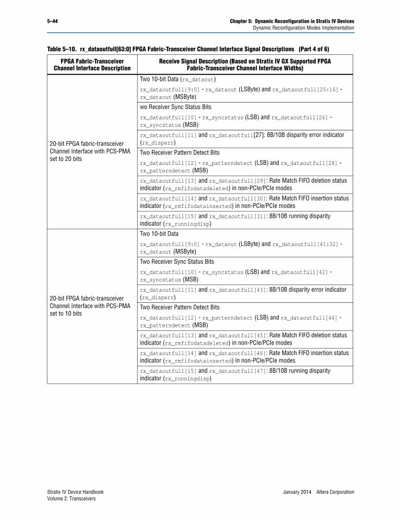
5–44 Chapter 5: Dynamic Reconfiguration in Stratix IV DevicesDynamic Reconfiguration Modes Implementation
20-bit FPGA fabric-transceiver Channel Interface with PCS-PMA set to 20 bits
Two 10-bit Data (rx_dataout)
rx_dataoutfull[9:0] - rx_dataout (LSByte) and rx_dataoutfull[25:16] - rx_dataout (MSByte)
wo Receiver Sync Status Bits
rx_dataoutfull[10] - rx_syncstatus (LSB) and rx_dataoutfull[26] - rx_syncstatus (MSB)
rx_dataoutfull[11] and rx_dataoutfull[27]: 8B/10B disparity error indicator (rx_disperr)
Two Receiver Pattern Detect Bits
rx_dataoutfull[12] - rx_patterndetect (LSB) and rx_dataoutfull[28] - rx_patterndetect (MSB)
rx_dataoutfull[13] and rx_dataoutfull[29]: Rate Match FIFO deletion status indicator (rx_rmfifodatadeleted) in non-PCIe/PCIe modes
rx_dataoutfull[14] and rx_dataoutfull[30]: Rate Match FIFO insertion status indicator (rx_rmfifodatainserted) in non-PCIe/PCIe modes
rx_dataoutfull[15] and rx_dataoutfull[31]: 8B/10B running disparity indicator (rx_runningdisp)
20-bit FPGA fabric-transceiver Channel Interface with PCS-PMA set to 10 bits
Two 10-bit Data
rx_dataoutfull[9:0] - rx_dataout (LSByte) and rx_dataoutfull[41:32] - rx_dataout (MSByte)
Two Receiver Sync Status Bits
rx_dataoutfull[10] - rx_syncstatus (LSB) and rx_dataoutfull[42] - rx_syncstatus (MSB)
rx_dataoutfull[11] and rx_dataoutfull[43]: 8B/10B disparity error indicator (rx_disperr)
Two Receiver Pattern Detect Bits
rx_dataoutfull[12] - rx_patterndetect (LSB) and rx_dataoutfull[44] - rx_patterndetect (MSB)
rx_dataoutfull[13] and rx_dataoutfull[45]: Rate Match FIFO deletion status indicator (rx_rmfifodatadeleted) in non-PCIe/PCIe modes
rx_dataoutfull[14] and rx_dataoutfull[46]: Rate Match FIFO insertion status indicator (rx_rmfifodatainserted) in non-PCIe/PCIe modes
rx_dataoutfull[15] and rx_dataoutfull[47]: 8B/10B running disparity indicator (rx_runningdisp)
Table 5–10. rx_dataoutfull[63:0] FPGA Fabric-Transceiver Channel Interface Signal Descriptions (Part 4 of 6)
FPGA Fabric-Transceiver Channel Interface Description
Receive Signal Description (Based on Stratix IV GX Supported FPGA Fabric-Transceiver Channel Interface Widths)
Stratix IV Device Handbook January 2014 Altera CorporationVolume 2: Transceivers
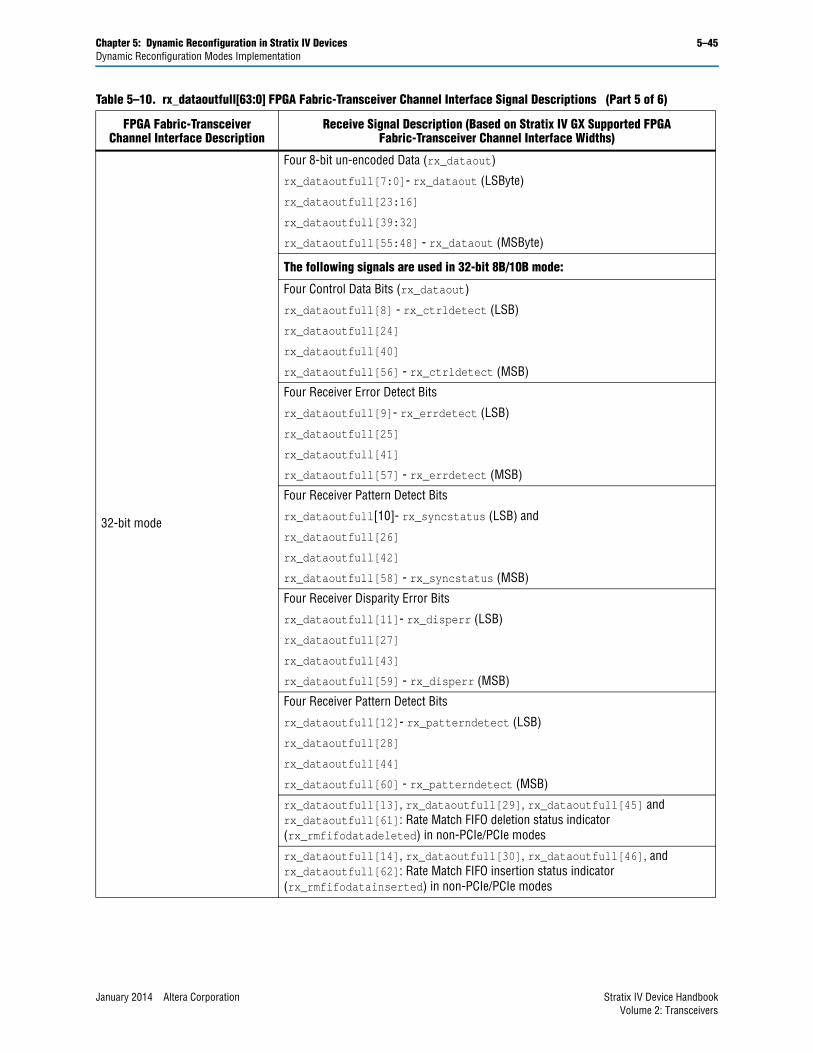
Chapter 5: Dynamic Reconfiguration in Stratix IV Devices 5–45Dynamic Reconfiguration Modes Implementation
32-bit mode
Four 8-bit un-encoded Data (rx_dataout)
rx_dataoutfull[7:0]- rx_dataout (LSByte)
rx_dataoutfull[23:16]
rx_dataoutfull[39:32]
rx_dataoutfull[55:48] - rx_dataout (MSByte)
The following signals are used in 32-bit 8B/10B mode:
Four Control Data Bits (rx_dataout)
rx_dataoutfull[8] - rx_ctrldetect (LSB)
rx_dataoutfull[24]
rx_dataoutfull[40]
rx_dataoutfull[56] - rx_ctrldetect (MSB)
Four Receiver Error Detect Bits
rx_dataoutfull[9]- rx_errdetect (LSB)
rx_dataoutfull[25]
rx_dataoutfull[41]
rx_dataoutfull[57] - rx_errdetect (MSB)
Four Receiver Pattern Detect Bits
rx_dataoutfull[10]- rx_syncstatus (LSB) and
rx_dataoutfull[26]
rx_dataoutfull[42]
rx_dataoutfull[58] - rx_syncstatus (MSB)
Four Receiver Disparity Error Bits
rx_dataoutfull[11]- rx_disperr (LSB)
rx_dataoutfull[27]
rx_dataoutfull[43]
rx_dataoutfull[59] - rx_disperr (MSB)
Four Receiver Pattern Detect Bits
rx_dataoutfull[12]- rx_patterndetect (LSB)
rx_dataoutfull[28]
rx_dataoutfull[44]
rx_dataoutfull[60] - rx_patterndetect (MSB)
rx_dataoutfull[13], rx_dataoutfull[29], rx_dataoutfull[45] and rx_dataoutfull[61]: Rate Match FIFO deletion status indicator (rx_rmfifodatadeleted) in non-PCIe/PCIe modes
rx_dataoutfull[14], rx_dataoutfull[30], rx_dataoutfull[46], and rx_dataoutfull[62]: Rate Match FIFO insertion status indicator (rx_rmfifodatainserted) in non-PCIe/PCIe modes
Table 5–10. rx_dataoutfull[63:0] FPGA Fabric-Transceiver Channel Interface Signal Descriptions (Part 5 of 6)
FPGA Fabric-Transceiver Channel Interface Description
Receive Signal Description (Based on Stratix IV GX Supported FPGA Fabric-Transceiver Channel Interface Widths)
January 2014 Altera Corporation Stratix IV Device HandbookVolume 2: Transceivers
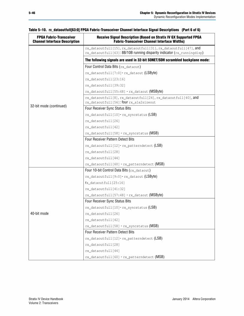
5–46 Chapter 5: Dynamic Reconfiguration in Stratix IV DevicesDynamic Reconfiguration Modes Implementation
32-bit mode (continued)
rx_dataoutfull[15], rx_dataoutfull[31], rx_dataoutfull[47], and rx_dataoutfull[63]: 8B/10B running disparity indicator (rx_runningdisp)
The following signals are used in 32-bit SONET/SDH scrambled backplane mode:
Four Control Data Bits (rx_dataout)
rx_dataoutfull[7:0]- rx_dataout (LSByte)
rx_dataoutfull[23:16]
rx_dataoutfull[39:32]
rx_dataoutfull[55:48] - rx_dataout (MSByte)
rx_dataoutfull[8], rx_dataoutfull[24], rx_dataoutfull[40], and rx_dataoutfull[56]: four rx_a1a2sizeout
Four Receiver Sync Status Bits
rx_dataoutfull[10]- rx_syncstatus (LSB)
rx_dataoutfull[26]
rx_dataoutfull[42]
rx_dataoutfull[58] - rx_syncstatus (MSB)
Four Receiver Pattern Detect Bits
rx_dataoutfull[12]- rx_patterndetect (LSB)
rx_dataoutfull[28]
rx_dataoutfull[44]
rx_dataoutfull[60] - rx_patterndetect (MSB)
40-bit mode
Four 10-bit Control Data Bits (rx_dataout)
rx_dataoutfull[9:0]- rx_dataout (LSByte)
rx_dataoutfull[25:16]
rx_dataoutfull[41:32]
rx_dataoutfull[57:48] - rx_dataout (MSByte)
Four Receiver Sync Status Bits
rx_dataoutfull[10]- rx_syncstatus (LSB)
rx_dataoutfull[26]
rx_dataoutfull[42]
rx_dataoutfull[58] - rx_syncstatus (MSB)
Four Receiver Pattern Detect Bits
rx_dataoutfull[12]- rx_patterndetect (LSB)
rx_dataoutfull[28]
rx_dataoutfull[44]
rx_dataoutfull[60] - rx_patterndetect (MSB)
Table 5–10. rx_dataoutfull[63:0] FPGA Fabric-Transceiver Channel Interface Signal Descriptions (Part 6 of 6)
FPGA Fabric-Transceiver Channel Interface Description
Receive Signal Description (Based on Stratix IV GX Supported FPGA Fabric-Transceiver Channel Interface Widths)
Stratix IV Device Handbook January 2014 Altera CorporationVolume 2: Transceivers
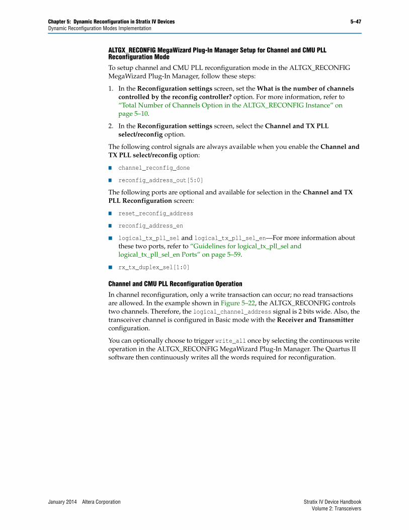
Chapter 5: Dynamic Reconfiguration in Stratix IV Devices 5–47Dynamic Reconfiguration Modes Implementation
ALTGX_RECONFIG MegaWizard Plug-In Manager Setup for Channel and CMU PLL Reconfiguration Mode
To setup channel and CMU PLL reconfiguration mode in the ALTGX_RECONFIG MegaWizard Plug-In Manager, follow these steps:
1. In the Reconfiguration settings screen, set the What is the number of channels controlled by the reconfig controller? option. For more information, refer to “Total Number of Channels Option in the ALTGX_RECONFIG Instance” on page 5–10.
2. In the Reconfiguration settings screen, select the Channel and TX PLL select/reconfig option.
The following control signals are always available when you enable the Channel and TX PLL select/reconfig option:
■ channel_reconfig_done
■ reconfig_address_out[5:0]
The following ports are optional and available for selection in the Channel and TX PLL Reconfiguration screen:
■ reset_reconfig_address
■ reconfig_address_en
■ logical_tx_pll_sel and logical_tx_pll_sel_en—For more information about these two ports, refer to “Guidelines for logical_tx_pll_sel and logical_tx_pll_sel_en Ports” on page 5–59.
■ rx_tx_duplex_sel[1:0]
Channel and CMU PLL Reconfiguration Operation
In channel reconfiguration, only a write transaction can occur; no read transactions are allowed. In the example shown in Figure 5–22, the ALTGX_RECONFIG controls two channels. Therefore, the logical_channel_address signal is 2 bits wide. Also, the transceiver channel is configured in Basic mode with the Receiver and Transmitter configuration.
You can optionally choose to trigger write_all once by selecting the continuous write operation in the ALTGX_RECONFIG MegaWizard Plug-In Manager. The Quartus II software then continuously writes all the words required for reconfiguration.
January 2014 Altera Corporation Stratix IV Device HandbookVolume 2: Transceivers
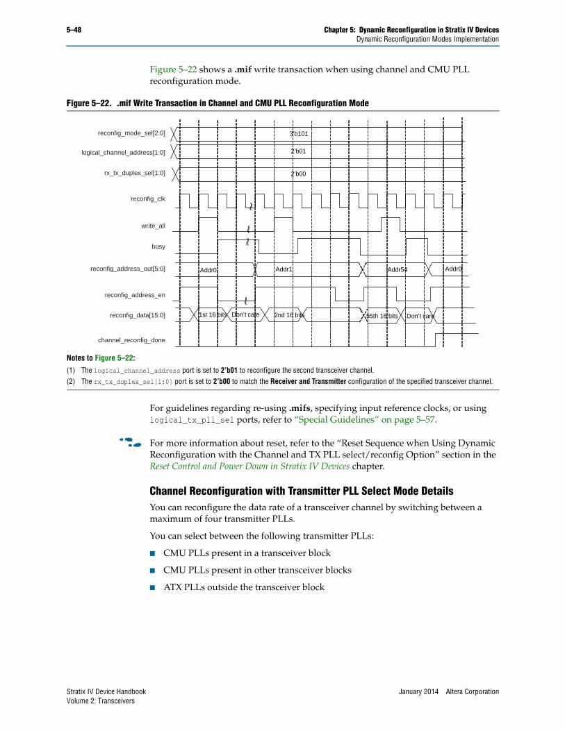
5–48 Chapter 5: Dynamic Reconfiguration in Stratix IV DevicesDynamic Reconfiguration Modes Implementation
Figure 5–22 shows a .mif write transaction when using channel and CMU PLL reconfiguration mode.
For guidelines regarding re-using .mifs, specifying input reference clocks, or using logical_tx_pll_sel ports, refer to “Special Guidelines” on page 5–57.
f For more information about reset, refer to the “Reset Sequence when Using Dynamic Reconfiguration with the Channel and TX PLL select/reconfig Option” section in the Reset Control and Power Down in Stratix IV Devices chapter.
Channel Reconfiguration with Transmitter PLL Select Mode DetailsYou can reconfigure the data rate of a transceiver channel by switching between a maximum of four transmitter PLLs.
You can select between the following transmitter PLLs:
■ CMU PLLs present in a transceiver block
■ CMU PLLs present in other transceiver blocks
■ ATX PLLs outside the transceiver block
Figure 5–22. .mif Write Transaction in Channel and CMU PLL Reconfiguration Mode
Notes to Figure 5–22:
(1) The logical_channel_address port is set to 2’b01 to reconfigure the second transceiver channel. (2) The rx_tx_duplex_sel[1:0] port is set to 2’b00 to match the Receiver and Transmitter configuration of the specified transceiver channel.
Addr0 Addr1
1st 16 bits Don’t care
Addr0Addr54
Don’t care
3’b101
2’b00
2’b01
reconfig_mode_sel[2:0]
logical_channel_address[1:0]
rx_tx_duplex_sel[1:0]
reconfig_clk
write_all
busy
reconfig_address_out[5:0]
reconfig_address_en
reconfig_data[15:0]
channel_reconfig_done
2nd 16 bits 55th 16 bits
Stratix IV Device Handbook January 2014 Altera CorporationVolume 2: Transceivers
Chapter 5: Dynamic Reconfiguration in Stratix IV Devices 5–49Dynamic Reconfiguration Modes Implementation
You can use the channel reconfiguration with transmitter PLL select mode along with the CMU PLL reconfiguration mode only if it is a CMU PLL and not an ATX PLL. You can first reconfigure the second CMU PLL to the desired data rate using CMU PLL reconfiguration mode. Then use channel reconfiguration with transmitter PLL select mode to reconfigure the transceiver channel to listen to the second CMU PLL.
For more information about supported configurations, refer to “Transceiver Channel Reconfiguration Mode Details” on page 5–19 and “Memory Initialization File (.mif)” on page 5–20.
1 Channel reconfiguration with transmitter PLL select mode is not applicable to regular transceiver channels in ×4 and ×8 bonded mode configurations.
For guidelines regarding re-using .mifs, specifying input reference clocks, or using the logical_tx_pll_sel ports, refer to “Special Guidelines” on page 5–57.
f For more information about reset, refer to the “Reset Sequence when Using Dynamic Reconfiguration with the Channel and TX PLL select/reconfig Option” section in the Reset Control and Power Down in Stratix IV Devices chapter.
Blocks Reconfigured in the Channel Reconfiguration with Transmitter PLL Select Mode
The blocks reconfigured in this mode have two types of multiplexers. When you switch between the CMU PLLs within the same transceiver block, the multiplexer that is reconfigured is within the transceiver block. It is located in the transmitter channel path.
January 2014 Altera Corporation Stratix IV Device HandbookVolume 2: Transceivers
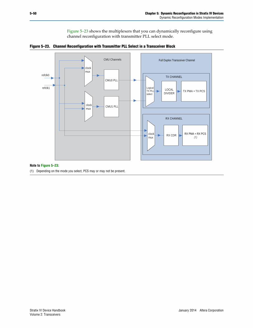
5–50 Chapter 5: Dynamic Reconfiguration in Stratix IV DevicesDynamic Reconfiguration Modes Implementation
Figure 5–23 shows the multiplexers that you can dynamically reconfigure using channel reconfiguration with transmitter PLL select mode.
Figure 5–23. Channel Reconfiguration with Transmitter PLL Select in a Transceiver Block
Note to Figure 5–23:
(1) Depending on the mode you select, PCS may or may not be present.
Full Duplex Transceiver Channel
TX CHANNEL
RX CHANNEL
CMU Channels
refclk0
refclk1
CMU0 PLL
CMU1 PLL
LogicalTX PLLselect
clockmux
LOCALDIVIDER
RX CDR
TX PMA + TX PCS
clockmux
clockmux
clockmux
RX PMA + RX PCS (1)
Stratix IV Device Handbook January 2014 Altera CorporationVolume 2: Transceivers
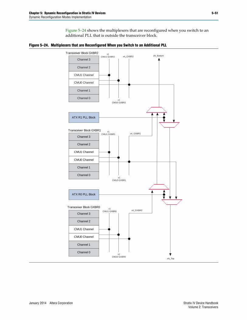
Chapter 5: Dynamic Reconfiguration in Stratix IV Devices 5–51Dynamic Reconfiguration Modes Implementation
Figure 5–24 shows the multiplexers that are reconfigured when you switch to an additional PLL that is outside the transceiver block.
Figure 5–24. Multiplexers that are Reconfigured When you Switch to an Additional PLL
Channel 3
Channel 2
CMU1 Channel
CMU0 Channel
Channel 1
Channel 0
ATX R0 PLL Block
Channel 3
Channel 2
CMU1 Channel
CMU0 Channel
Channel 1
Channel 0
ATX R1 PLL Block
Channel 3
Channel 2
CMU1 Channel
CMU0 Channel
Channel 1
Channel 0
Transceiver Block GXBR0
Transceiver Block GXBR1
Transceiver Block GXBR2
xN_Top
x1CMU0 GXBR0
x1CMU1 GXBR0 x4_GXBR0
x1CMU0 GXBR1
x1CMU1 GXBR1 x4_GXBR1
x1CMU0 GXBR2
x1CMU1 GXBR2 x4_GXBR2 xN_Bottom
January 2014 Altera Corporation Stratix IV Device HandbookVolume 2: Transceivers
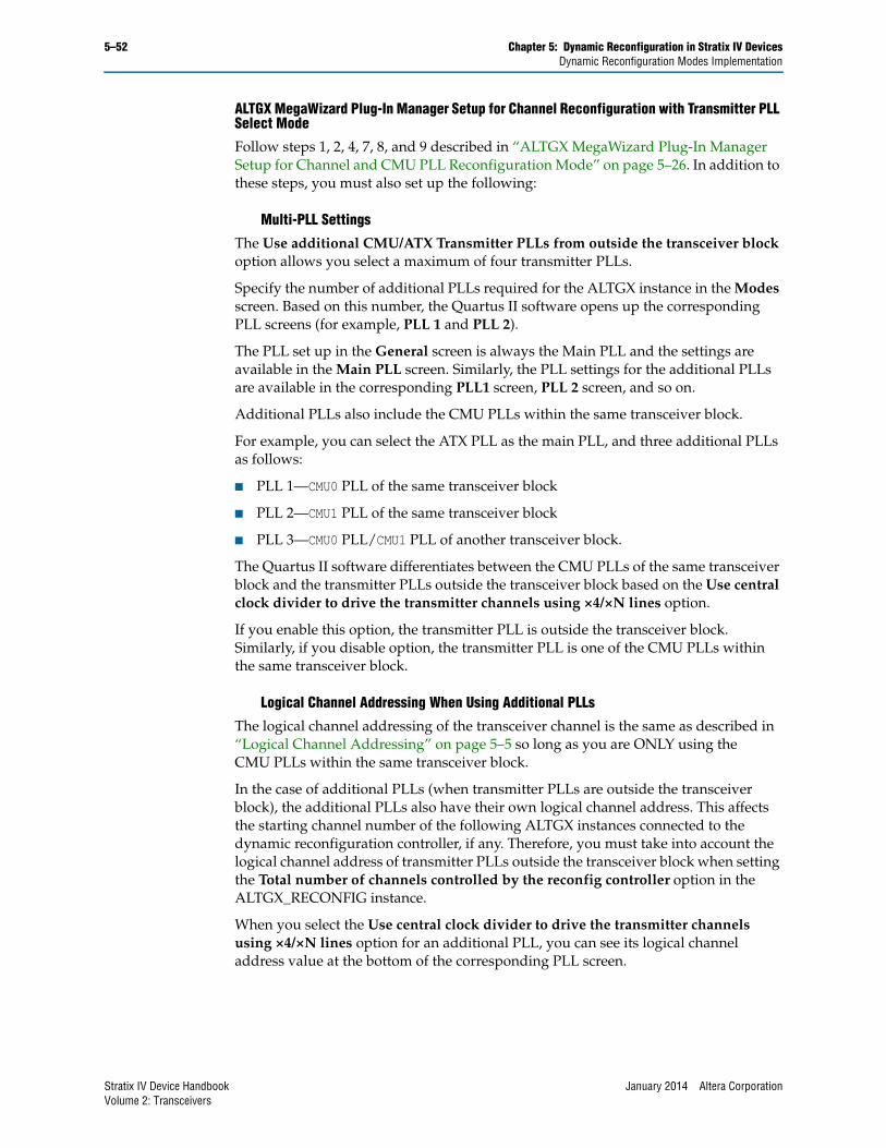
5–52 Chapter 5: Dynamic Reconfiguration in Stratix IV DevicesDynamic Reconfiguration Modes Implementation
ALTGX MegaWizard Plug-In Manager Setup for Channel Reconfiguration with Transmitter PLL Select Mode
Follow steps 1, 2, 4, 7, 8, and 9 described in “ALTGX MegaWizard Plug-In Manager Setup for Channel and CMU PLL Reconfiguration Mode” on page 5–26. In addition to these steps, you must also set up the following:
Multi-PLL Settings
The Use additional CMU/ATX Transmitter PLLs from outside the transceiver block option allows you select a maximum of four transmitter PLLs.
Specify the number of additional PLLs required for the ALTGX instance in the Modes screen. Based on this number, the Quartus II software opens up the corresponding PLL screens (for example, PLL 1 and PLL 2).
The PLL set up in the General screen is always the Main PLL and the settings are available in the Main PLL screen. Similarly, the PLL settings for the additional PLLs are available in the corresponding PLL1 screen, PLL 2 screen, and so on.
Additional PLLs also include the CMU PLLs within the same transceiver block.
For example, you can select the ATX PLL as the main PLL, and three additional PLLs as follows:
■ PLL 1—CMU0 PLL of the same transceiver block
■ PLL 2—CMU1 PLL of the same transceiver block
■ PLL 3—CMU0 PLL/CMU1 PLL of another transceiver block.
The Quartus II software differentiates between the CMU PLLs of the same transceiver block and the transmitter PLLs outside the transceiver block based on the Use central clock divider to drive the transmitter channels using ×4/×N lines option.
If you enable this option, the transmitter PLL is outside the transceiver block. Similarly, if you disable option, the transmitter PLL is one of the CMU PLLs within the same transceiver block.
Logical Channel Addressing When Using Additional PLLs
The logical channel addressing of the transceiver channel is the same as described in “Logical Channel Addressing” on page 5–5 so long as you are ONLY using the CMU PLLs within the same transceiver block.
In the case of additional PLLs (when transmitter PLLs are outside the transceiver block), the additional PLLs also have their own logical channel address. This affects the starting channel number of the following ALTGX instances connected to the dynamic reconfiguration controller, if any. Therefore, you must take into account the logical channel address of transmitter PLLs outside the transceiver block when setting the Total number of channels controlled by the reconfig controller option in the ALTGX_RECONFIG instance.
When you select the Use central clock divider to drive the transmitter channels using ×4/×N lines option for an additional PLL, you can see its logical channel address value at the bottom of the corresponding PLL screen.
Stratix IV Device Handbook January 2014 Altera CorporationVolume 2: Transceivers
Chapter 5: Dynamic Reconfiguration in Stratix IV Devices 5–53Dynamic Reconfiguration Modes Implementation
Selecting the PLL Logical Reference Index for Additional PLLs
The PLL logical reference index of additional PLLs outside the transceiver block can only be 2 or 3.
■ When you enable the Use central clock divider to drive the transmitter channels using ×4/×N lines option for an additional PLL, you can only select between 2 or 3 as the PLL logical reference index.
■ When you disable the Use central clock divider to drive the transmitter channels using ×4/×N lines option for an additional PLL, the additional PLL is one of the CMU PLLs within the same transceiver block. Therefore, the PLL logical reference index is either 0 or 1.
For more information about the PLL logical reference index of CMU PLLs within the same transceiver block, refer to “Selecting the Logical Reference Index of the CMU PLL” on page 5–29.
ALTGX_RECONFIG MegaWizard Plug-In Manager Setup for Channel Reconfiguration with Transmitter PLL Select Mode
For more information, refer to the “ALTGX_RECONFIG MegaWizard Plug-In Manager Setup for Channel and CMU PLL Reconfiguration Mode” on page 5–47.
Channel Reconfiguration with Transmitter PLL Select Operation
Read transactions are not allowed in this mode.
Figure 5–25 shows a .mif write transaction when dynamically reconfiguring a transceiver channel. The .mif write transaction in channel reconfiguration with transmitter PLL select mode remains the same except for the reconfig_mode_sel[2:0] value and the difference in the number of .mif words used. In this example, the transceiver channel is configured in Receiver and Transmitter configuration. Therefore, the .mif size is 8.
You can optionally choose to trigger write_all once by selecting the continuous write operation in the ALTGX_RECONFIG MegaWizard Plug-In Manager. The Quartus II software then continuously writes all the words required for reconfiguration.
January 2014 Altera Corporation Stratix IV Device HandbookVolume 2: Transceivers
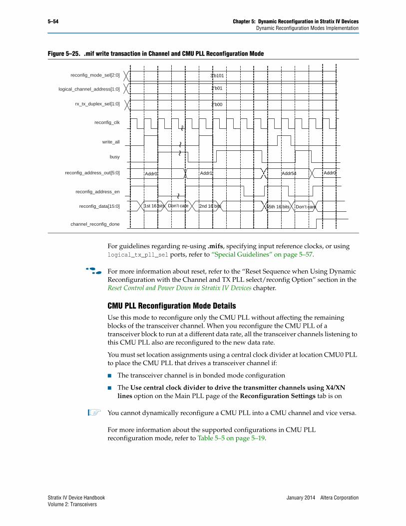
5–54 Chapter 5: Dynamic Reconfiguration in Stratix IV DevicesDynamic Reconfiguration Modes Implementation
For guidelines regarding re-using .mifs, specifying input reference clocks, or using logical_tx_pll_sel ports, refer to “Special Guidelines” on page 5–57.
f For more information about reset, refer to the “Reset Sequence when Using Dynamic Reconfiguration with the Channel and TX PLL select/reconfig Option” section in the Reset Control and Power Down in Stratix IV Devices chapter.
CMU PLL Reconfiguration Mode DetailsUse this mode to reconfigure only the CMU PLL without affecting the remaining blocks of the transceiver channel. When you reconfigure the CMU PLL of a transceiver block to run at a different data rate, all the transceiver channels listening to this CMU PLL also are reconfigured to the new data rate.
You must set location assignments using a central clock divider at location CMU0 PLL to place the CMU PLL that drives a transceiver channel if:
■ The transceiver channel is in bonded mode configuration
■ The Use central clock divider to drive the transmitter channels using X4/XN lines option on the Main PLL page of the Reconfiguration Settings tab is on
1 You cannot dynamically reconfigure a CMU PLL into a CMU channel and vice versa.
For more information about the supported configurations in CMU PLL reconfiguration mode, refer to Table 5–5 on page 5–19.
Figure 5–25. .mif write transaction in Channel and CMU PLL Reconfiguration Mode
Addr0 Addr1
1st 16 bits Don’t care
Addr0Addr54
Don’t care
3’b101
2’b00
2’b01
reconfig_mode_sel[2:0]
logical_channel_address[1:0]
rx_tx_duplex_sel[1:0]
reconfig_clk
write_all
busy
reconfig_address_out[5:0]
reconfig_address_en
reconfig_data[15:0]
channel_reconfig_done
2nd 16 bits 55th 16 bits
Stratix IV Device Handbook January 2014 Altera CorporationVolume 2: Transceivers
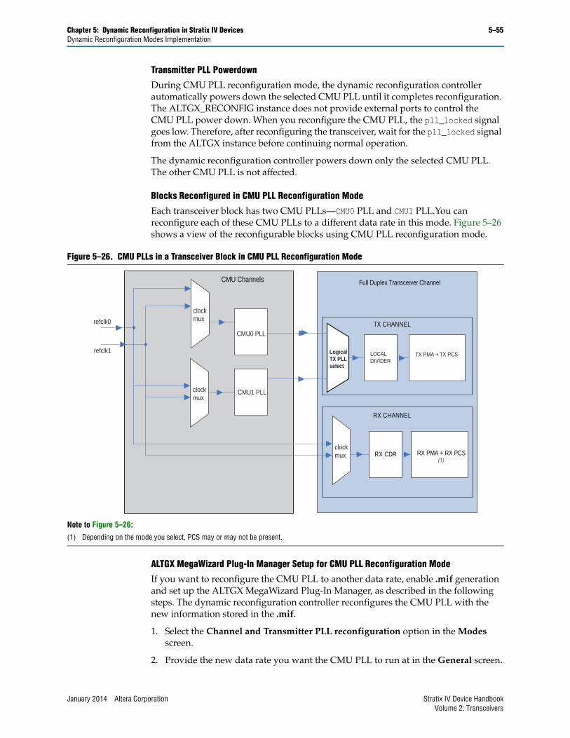
Chapter 5: Dynamic Reconfiguration in Stratix IV Devices 5–55Dynamic Reconfiguration Modes Implementation
Transmitter PLL Powerdown
During CMU PLL reconfiguration mode, the dynamic reconfiguration controller automatically powers down the selected CMU PLL until it completes reconfiguration. The ALTGX_RECONFIG instance does not provide external ports to control the CMU PLL power down. When you reconfigure the CMU PLL, the pll_locked signal goes low. Therefore, after reconfiguring the transceiver, wait for the pll_locked signal from the ALTGX instance before continuing normal operation.
The dynamic reconfiguration controller powers down only the selected CMU PLL. The other CMU PLL is not affected.
Blocks Reconfigured in CMU PLL Reconfiguration Mode
Each transceiver block has two CMU PLLs—CMU0 PLL and CMU1 PLL.You can reconfigure each of these CMU PLLs to a different data rate in this mode. Figure 5–26 shows a view of the reconfigurable blocks using CMU PLL reconfiguration mode.
ALTGX MegaWizard Plug-In Manager Setup for CMU PLL Reconfiguration Mode
If you want to reconfigure the CMU PLL to another data rate, enable .mif generation and set up the ALTGX MegaWizard Plug-In Manager, as described in the following steps. The dynamic reconfiguration controller reconfigures the CMU PLL with the new information stored in the .mif.
1. Select the Channel and Transmitter PLL reconfiguration option in the Modes screen.
2. Provide the new data rate you want the CMU PLL to run at in the General screen.
Figure 5–26. CMU PLLs in a Transceiver Block in CMU PLL Reconfiguration Mode
Note to Figure 5–26:
(1) Depending on the mode you select, PCS may or may not be present.
Full Duplex Transceiver Channel
RX CDR
TX CHANNEL
RX CHANNEL
CMU Channels
refclk0
refclk1
CMU0 PLL
CMU1 PLL
LOCALDIVIDER
TX PMA + TX PCS LogicalTX PLLselect
clockmux
clockmux
clockmux
RX PMA + RX PCS(1)
January 2014 Altera Corporation Stratix IV Device HandbookVolume 2: Transceivers
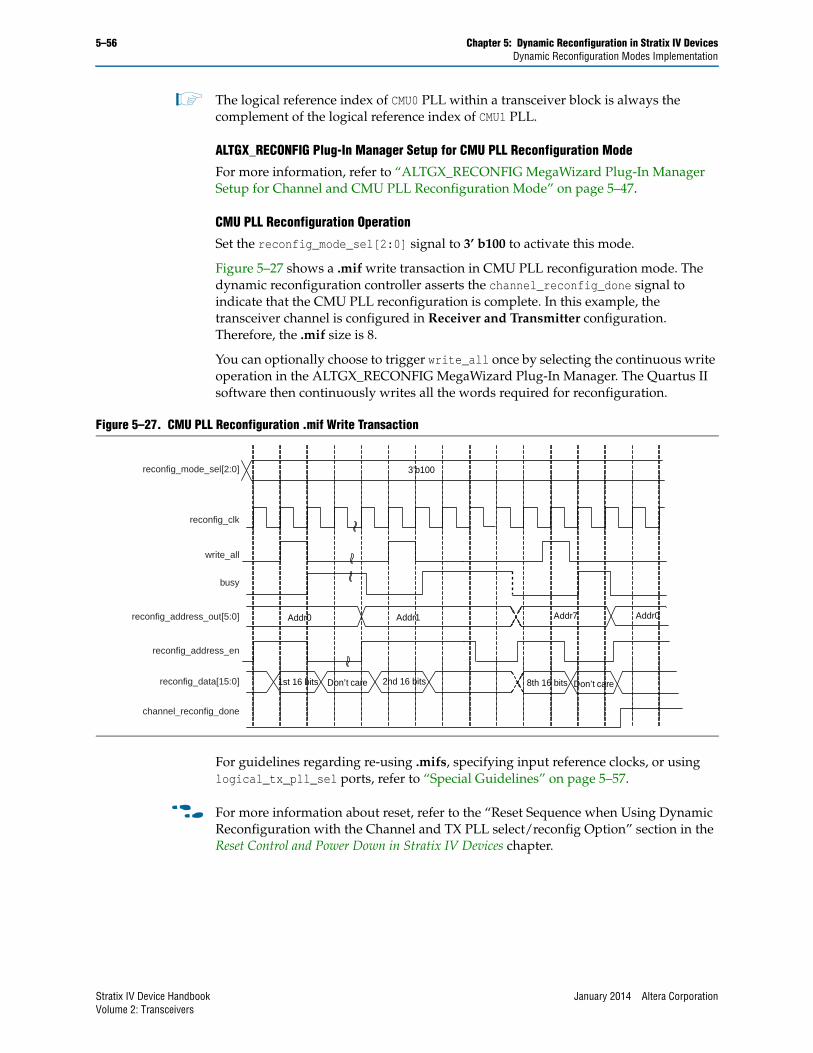
5–56 Chapter 5: Dynamic Reconfiguration in Stratix IV DevicesDynamic Reconfiguration Modes Implementation
1 The logical reference index of CMU0 PLL within a transceiver block is always the complement of the logical reference index of CMU1 PLL.
ALTGX_RECONFIG Plug-In Manager Setup for CMU PLL Reconfiguration Mode
For more information, refer to “ALTGX_RECONFIG MegaWizard Plug-In Manager Setup for Channel and CMU PLL Reconfiguration Mode” on page 5–47.
CMU PLL Reconfiguration Operation
Set the reconfig_mode_sel[2:0] signal to 3’ b100 to activate this mode.
Figure 5–27 shows a .mif write transaction in CMU PLL reconfiguration mode. The dynamic reconfiguration controller asserts the channel_reconfig_done signal to indicate that the CMU PLL reconfiguration is complete. In this example, the transceiver channel is configured in Receiver and Transmitter configuration. Therefore, the .mif size is 8.
You can optionally choose to trigger write_all once by selecting the continuous write operation in the ALTGX_RECONFIG MegaWizard Plug-In Manager. The Quartus II software then continuously writes all the words required for reconfiguration.
For guidelines regarding re-using .mifs, specifying input reference clocks, or using logical_tx_pll_sel ports, refer to “Special Guidelines” on page 5–57.
f For more information about reset, refer to the “Reset Sequence when Using Dynamic Reconfiguration with the Channel and TX PLL select/reconfig Option” section in the Reset Control and Power Down in Stratix IV Devices chapter.
Figure 5–27. CMU PLL Reconfiguration .mif Write Transaction
Addr0 Addr1
Don’t care
Addr0Addr7
8th 16 bits Don’t care
3’b100reconfig_mode_sel[2:0]
reconfig_clk
write_all
busy
reconfig_address_out[5:0]
reconfig_address_en
reconfig_data[15:0]
channel_reconfig_done
2nd 16 bits1st 16 bits
Stratix IV Device Handbook January 2014 Altera CorporationVolume 2: Transceivers
Chapter 5: Dynamic Reconfiguration in Stratix IV Devices 5–57Dynamic Reconfiguration Modes Implementation
Central Control Unit Reconfiguration Mode DetailsCentral control unit reconfiguration mode is a .mif-based mode used to reconfigure the central control unit (CCU) of the transceiver. Use reconfig_mode_sel[] to activate this mode. Central control unit reconfiguration mode is applicable for bonded PCS configurations such as Basic ×4 and ×8, XAUI, and PCIe ×4 and ×8. For the allowed configurations, refer to Table 5–5 on page 5–19.
For instance, to dynamically reconfigure an ALTGX instance in Basic ×4 configuration to a XAUI configuration, you must first configure:
1. The transceiver channel and CMU PLL to run at the XAUI data rate and functional mode (use channel and CMU PLL reconfiguration mode).
2. Reconfigure the central control unit portion of the transceiver from Basic to XAUI functional mode (use central control unit reconfiguration mode). For more information about the central control unit reconfiguration mode, refer to “Example 2” on page 5–100.
1 Dynamic reconfiguration is not available if hard IP is used in PCIe mode.
1 To switch between one bonded PCS configuration and another, always use:
1) Channel and CMU PLL reconfiguration mode followed by
2) Central control unit reconfiguration mode
Use the same .mif for both the these steps. In step 1, a partial .mif is written and the remaining contents of the .mif is written in step 2. In step 1, reconfigure all the channels one-by-one. In step-2, reconfiguration of the central control unit is transceiver-block based. Reconfigure any one of the four channels in the transceiver block.
Special GuidelinesThe following section describes the special guidelines required for the transceiver channel reconfiguration modes previously described. This section includes the following:
■ “Guidelines for Re-Using .mifs” on page 5–57
■ “Guidelines for logical_tx_pll_sel and logical_tx_pll_sel_en Ports” on page 5–59
■ “Guidelines for Specifying the Input Reference Clocks” on page 5–61
Guidelines for Re-Using .mifs
To configure the transceiver PLLs and receiver CDRs for multiple data rates, it is important to understand the input reference clock requirements. This helps you to efficiently create the clocking scheme for reconfiguration and to reuse the .mifs across all channels in the device. This section describes the clocking enhancements and the implications of using input clocks from various clock sources.
The available clock inputs appear as a pll_inclk_rx_cruclk[] port and can be provided from the inter-transceiver block lines (also known as ITB lines), from the global clock networks that are driven by an input pin or by a PLL cascade clock.
January 2014 Altera Corporation Stratix IV Device HandbookVolume 2: Transceivers
5–58 Chapter 5: Dynamic Reconfiguration in Stratix IV DevicesDynamic Reconfiguration Modes Implementation
f For more information about input reference clocking, refer to the “Input Reference Clocking” section of the Transceiver Clocking in Stratix IV Devices chapter.
The following section describes the clocking requirements to re-use .mifs.
The .mif contains information about the input clock multiplexer settings and the functional blocks that you selected during the ALTGX MegaWizard Plug-In Manager instantiation. You can use a .mif to dynamically reconfigure any of the other transceiver channels in the device as long as the order of the clock inputs is consistent. For example, assume that a .mif is generated for a transceiver channel in transceiver block 0 and the input clock source is connected to the pll_inclk_rx_cruclk[0] port. When you use the generated .mif for a channel in other transceiver blocks (for example, transceiver block 1), the same clock source must be connected to the pll_inclk_rx_cruclk[0] port. Figure 5–28 and Figure 5–29 show the incorrect and correct order of input reference clocks, respectively.
In Figure 5–28, the clocking is incorrect when re-using the .mif because the input reference clock is not connected to the corresponding pll_inclk_rx_cruclk[] ports in the two instances.
Figure 5–28. Incorrect Input Reference Clock Connections When Reusing a .mif
Note to Figure 5–28:
(1) The red lines represent the alternate source of REFCLK.
ALTGXInstance 1
Stratix IV GX Device
156.25 MHz
125 MHz
Transceiver Block 0
Transceiver Block 1
ALTGXInstance 2
pll_inclk_rx_cruclk[0]
pll_inclk_rx_cruclk[1]
pll_inclk_rx_cruclk[0]
pll_inclk_rx_cruclk[1]
(1)
(1)
Stratix IV Device Handbook January 2014 Altera CorporationVolume 2: Transceivers
Chapter 5: Dynamic Reconfiguration in Stratix IV Devices 5–59Dynamic Reconfiguration Modes Implementation
Figure 5–29 shows the correct input reference clock connections when re-using a .mif.
1 You can re-use the .mif generated for a transceiver channel on one side of the device for a transceiver channel on the other side of the device, only if the input reference clock frequencies and order of the pll_inclk_rx_cruclk[] ports in the ALTGX instances on both sides are identical.
In addition to the input reference clock requirements when re-using a .mif, refer to “Guidelines for logical_tx_pll_sel and logical_tx_pll_sel_en Ports” on page 5–59 for additional ways to re-use a .mif.
Guidelines for logical_tx_pll_sel and logical_tx_pll_sel_en Ports
This section describes when to enable the logical_tx_pll_sel and logical_tx_pll_sel_en ports and how to use them in the following dynamic reconfiguration modes:
■ Channel and CMU PLL reconfiguration mode
■ Channel reconfiguration with transmitter PLL select mode
■ CMU PLL reconfiguration mode
These are optional input ports to the ALTGX_RECONFIG instance.
Figure 5–29. Correct Input Reference Clock Connections When Reusing a .mif
Note to Figure 5–29:
(1) The red lines represent the alternate source of REFCLK.
Stratix IV GX Device
156.25 MHz
125 MHz
Transceiver Block 0
Transceiver Block 1
ALTGXInstance 1
ALTGXInstance 2
pll_inclk_rx_cruclk[0]
pll_inclk_rx_cruclk[1]
pll_inclk_rx_cruclk[1]
pll_inclk_rx_cruclk[0]
(1)
(1)
January 2014 Altera Corporation Stratix IV Device HandbookVolume 2: Transceivers
5–60 Chapter 5: Dynamic Reconfiguration in Stratix IV DevicesDynamic Reconfiguration Modes Implementation
Table 5–11 shows the conditions under which the dynamic reconfiguration controller uses either the logical_tx_pll_sel port value or the logical reference index value stored in the .mif.
Figure 5–30 shows the logical_tx_pll_sel and logical_tx_pll_sel_en ports.
Table 5–11 lists how the dynamic reconfiguration controller selects between the logical reference index stored in the .mif (logical tx pll) and the logical reference index specified at the logical_tx_pll_sel port.
Altera recommends keeping track of the transmitter PLL that drives the channel when you configure a transceiver channel in the ALTGX MegaWizard Plug-In Manager.
1 The logical_tx_pll_sel port does not modify transceiver settings on the receiver side.
If both the logical_tx_pll_sel and logical_tx_pll_sel_en ports are enabled, reconfigure the transmitter PLL. Keep the logical_tx_pll_sel and logical_tx_pll_sel_en signals at a constant logic level until the dynamic reconfiguration controller asserts the channel_reconfig_done signal.
Figure 5–30. Using logical_tx_pll_sel and logical_tx_pll_sel_en Ports
logical tx pll(logical reference
index value stored in the .mif)
logical_tx_pll_sel(logical reference indexspecified on the port)
logical_tx_pll_sel_en
ALTGX_RECONFIGinstance
selectedlogical reference index
value
0
1
Table 5–11. Various Combinations of the logical_tx_pll_sel and logical_tx_pll_sel_en Ports
logical_tx_pll_sel logical_tx_pll_sel_en Logical Reference Index Value Selected by the ALTGX_RECONFIG Instance
enabled enabled and value is 1 Value on the logical_tx_pll_sel port
enabled enabled and value is 0 logical reference index value stored in the .mif (logical tx pll)
enabled disabled Value on the logical_tx_pll_sel port
disabled disabled logical reference index value stored in the .mif (logical tx pll)
Stratix IV Device Handbook January 2014 Altera CorporationVolume 2: Transceivers
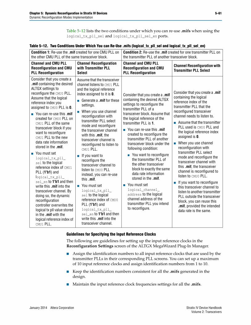
Chapter 5: Dynamic Reconfiguration in Stratix IV Devices 5–61Dynamic Reconfiguration Modes Implementation
Table 5–12 lists the two conditions under which you can re-use .mifs when using the logical_tx_pll_sel and logical_tx_pll_sel_en ports.
Guidelines for Specifying the Input Reference Clocks
The following are guidelines for setting up the input reference clocks in the Reconfiguration Settings screen of the ALTGX MegaWizard Plug-In Manager.
■ Assign the identification numbers to all input reference clocks that are used by the transmitter PLLs in their corresponding PLL screens. You can set up a maximum of 10 input reference clocks and assign identification numbers from 1 to 10.
■ Keep the identification numbers consistent for all the .mifs generated in the design.
■ Maintain the input reference clock frequencies settings for all the .mifs.
Table 5–12. Two Conditions Under Which You can Re-Use .mifs (logical_tx_pll_sel and logical_tx_pll_sel_en)
Condition 1: Re-use the .mif created for one CMU PLL on the other CMU PLL of the same transceiver block.
Condition 2: Re-use the .mif created for one transmitter PLL on the transmitter PLL of another transceiver block.
Channel and CMU PLL Reconfiguration and CMU PLL Reconfiguration
Channel Reconfiguration with Transmitter PLL Select
Channel and CMU PLL Reconfiguration and CMU PLL Reconfiguration
Channel Reconfiguration with Transmitter PLL Select
Consider that you create a .mif containing the desired ALTGX settings to reconfigure the CMU0 PLL. Assume that the logical reference index you assigned to CMU0 PLL is 0.
■ You can re-use this .mif created for CMU0 PLL on CMU1 PLL of the same transceiver block if you want to reconfigure CMU1 PLL to the new data rate information stored in the .mif.
■ You must set logical_tx_pll_sel to the logical reference index of CMU1 PLL (1'b1) and logical_tx_pll_sel_en to 1'b1 and then write this .mif into the transceiver channel. By doing so, the dynamic reconfiguration controller overwrites the logical tx pll value stored in the .mif with the logical reference index of CMU1 PLL.
Assume that the transceiver channel listens to CMU1 PLL and the logical reference index assigned to it is 0.
■ Generate a .mif for these settings.
■ When you use channel reconfiguration with transmitter PLL select mode and reconfigure the transceiver channel with this .mif, the transceiver channel is reconfigured to listen to CMU1 PLL.
■ If you want to reconfigure the transceiver channel to listen to CMU0 PLL instead, you can re-use this .mif.
■ You must set logical_tx_pll_sel to the logical reference index of CMU0 PLL (1'b1) and logical_tx_pll_sel_en to 1'b1 and then write this .mif into the transceiver channel.
Consider that you create a .mif containing the desired ALTGX settings to reconfigure the transmitter PLL of a transceiver block. Assume that the logical reference of the transmitter PLL is 1.
■ You can re-use this .mif created to reconfigure the transmitter PLL of another transceiver block under the following condition:
■ You want to reconfigure the transmitter PLL of the other transceiver block to exactly the same data rate information stored in the .mif.
■ You must set logical_channel_address to the logical channel address of the transmitter PLL you intend to reconfigure.
Consider that you create a .mif containing the logical reference index of the transmitter PLL that the reconfigured transceiver channel needs to listen to.
■ Assume that the transmitter PLL used is CMU0 PLL and the logical reference index assigned is 0.
■ When you use channel reconfiguration with transmitter PLL select mode and reconfigure the transceiver channel with this .mif, the transceiver channel is reconfigured to listen to CMU0 PLL.
■ If you want to reconfigure this transceiver channel to listen to another transmitter PLL outside the transceiver block, you can reuse this .mif, provided the intended data rate is the same.
January 2014 Altera Corporation Stratix IV Device HandbookVolume 2: Transceivers
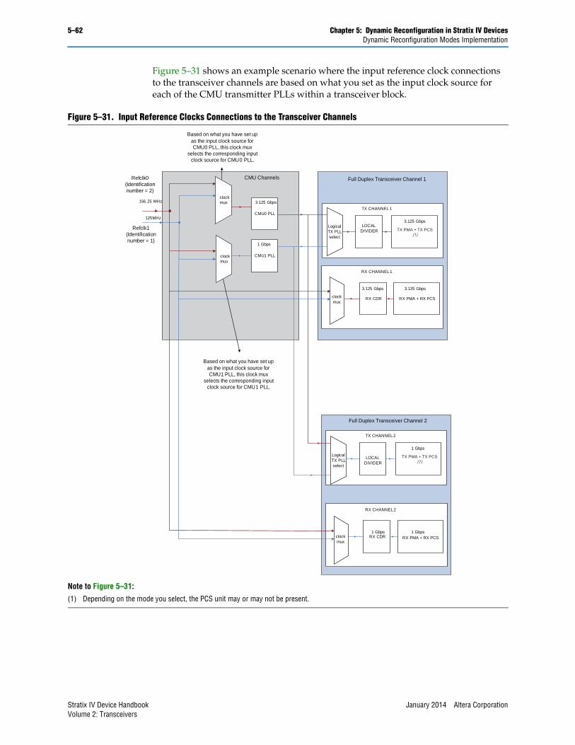
5–62 Chapter 5: Dynamic Reconfiguration in Stratix IV DevicesDynamic Reconfiguration Modes Implementation
Figure 5–31 shows an example scenario where the input reference clock connections to the transceiver channels are based on what you set as the input clock source for each of the CMU transmitter PLLs within a transceiver block.
Figure 5–31. Input Reference Clocks Connections to the Transceiver Channels
Note to Figure 5–31:
(1) Depending on the mode you select, the PCS unit may or may not be present.
Full Duplex Transceiver Channel 1
CMU0 PLL
RX CDR
CMU1 PLL
TX CHANNEL 1
Logical TX PLL select
RX CHANNEL 1
156 .25 MHz
125MHz
Refclk0 (Identification number = 2)
Refclk1 (Identification number = 1)
3.125 Gbps
3.125 Gbps 3.125 Gbps
LOCAL DIVIDER
3.125 Gbps
1 Gbps
CMU Channels
clock mux
Full Duplex Transceiver Channel 2
RX CDR
TX CHANNEL 2
Logical TX PLL select
RX CHANNEL 2
1 Gbps
1 Gbps 1 Gbps
LOCAL DIVIDER
clock mux
Based on what you have set up as the input clock source for CMU1 PLL, this clock mux
selects the corresponding input clock source for CMU1 PLL.
Based on what you have set up as the input clock source for CMU0 PLL, this clock mux
selects the corresponding input clock source for CMU0 PLL.
clockmux
clockmux
TX PMA + TX PCS (1)
TX PMA + TX PCS (1)
RX PMA + RX PCS
RX PMA + RX PCS
Stratix IV Device Handbook January 2014 Altera CorporationVolume 2: Transceivers
Chapter 5: Dynamic Reconfiguration in Stratix IV Devices 5–63Dynamic Reconfiguration Modes Implementation
Data Rate Division in Transmitter Mode DetailsYou can use data rate division in transmitter mode to modify the data rate of the transmitter channel in multiples of 1, 2, and 4. This dynamic reconfiguration mode is available only for the transmit side and not for the receive side.
Blocks Reconfigured in the Data Rate Division in Transmitter Mode
The only block that is reconfigured by the data rate division in transmitter mode is the transmitter local divider block of a transmitter channel. You can set the transmitter local divider to a divide by value of /1, /2, or /4, as shown in Figure 5–32.
You must be aware of the device operating range before you enable and use this feature. There are no legal checks that are imposed by the Quartus II software because it is an on-the-fly control feature. You must ensure that a specific functional mode supports the data rate range before dividing the clock when using this rate switch option.
1 Data rate division in transmitter mode is applicable only to channels configured in non-bonded mode clocked by the CMU0/CMU1 located within the same transceiver block.
ALTGX MegaWizard Plug-In Manager Setup for Data Rate Division in Transmitter Mode
Enable the following settings in the ALTGX MegaWizard Plug-In Manager:
1. Select the Channel and Transmitter PLL Reconfiguration option in the Reconfig screen to enable the ALTGX_RECONFIG instance to modify the transmitter channel local divider values dynamically.
2. Set the What is the starting channel number? option in the Reconfig screen. For more information, refer to “Logical Channel Addressing” on page 5–5.
The alternate reference clock is not required because a single clock source is used. The /1, /2, or /4 data rates can be derived from the single input reference clock.
Figure 5–32. Local Divider of a Transmitter Channel
High-Speed clockfrom TX PLL0
High-Speed clockfrom TX PLL1
/n
/1, /2, or /4
/4, /5, /8, or /10
High-Speed Serial Clock
Low-Speed Parallel Clock
January 2014 Altera Corporation Stratix IV Device HandbookVolume 2: Transceivers
5–64 Chapter 5: Dynamic Reconfiguration in Stratix IV DevicesDynamic Reconfiguration Modes Implementation
ALTGX_RECONFIG MegaWizard Plug-In Manager Setup for Data Rate Division in Transmitter Mode
Enable the following settings in the ALTGX_RECONFIG MegaWizard Plug-In Manager for data rate division in transmitter mode:
1. In the Reconfiguration settings screen, set the What is the number of channels controlled by the reconfig controller? option. For more information, refer to “Total Number of Channels Option in the ALTGX_RECONFIG Instance” on page 5–10.
2. Specify the logical channel address of the transmitter channel at the logical_channel_address input port.
3. In the Reconfiguration settings screen, select the Data rate division in TX option.
The rate_switch_ctrl[1:0] input port is available when you enable the Data rate division in TX option. The value you set at the rate_switch_ctrl[1:0] signal determines the transmitter local divider settings, as explained in “Dynamic Reconfiguration Controller Port List” on page 5–78.
To read the existing local divider settings of the transmitter channel, select the Use 'rate_switch_out' port to read out the current data rate division option in the Error checks/Data rate switch screen.
Decoding for the rate_switch_out[1:0] output signal is the same as the rate_switch_ctrl[1:0] input signal.
1 Dynamic rate switch has no effect on the dividers on the receive side of the transceiver channel. It can be used only for the transmitter.
1 Data rate division in transmitter mode does not require a .mif.
Data Rate Division in Transmitter Operation
The following sections describe the steps involved in write and read transactions for the data rate division in transmitter mode.
Stratix IV Device Handbook January 2014 Altera CorporationVolume 2: Transceivers
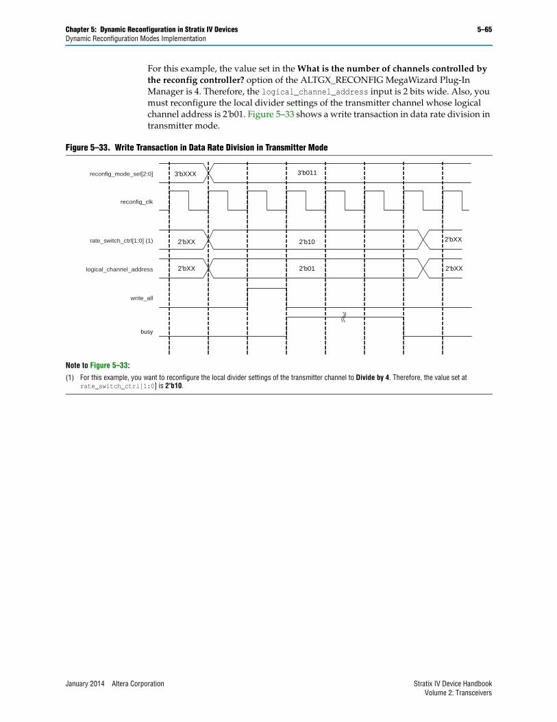
Chapter 5: Dynamic Reconfiguration in Stratix IV Devices 5–65Dynamic Reconfiguration Modes Implementation
For this example, the value set in the What is the number of channels controlled by the reconfig controller? option of the ALTGX_RECONFIG MegaWizard Plug-In Manager is 4. Therefore, the logical_channel_address input is 2 bits wide. Also, you must reconfigure the local divider settings of the transmitter channel whose logical channel address is 2'b01. Figure 5–33 shows a write transaction in data rate division in transmitter mode.
Figure 5–33. Write Transaction in Data Rate Division in Transmitter Mode
Note to Figure 5–33:
(1) For this example, you want to reconfigure the local divider settings of the transmitter channel to Divide by 4. Therefore, the value set at rate_switch_ctrl[1:0] is 2'b10.
busy
2'bXX 2'b01
2'bXX 2'b10 2'bXX
2'bXX
3'b0113'bXXXreconfig_mode_sel[2:0]
reconfig_clk
rate_switch_ctrl[1:0] (1)
logical_channel_address
write_all
January 2014 Altera Corporation Stratix IV Device HandbookVolume 2: Transceivers
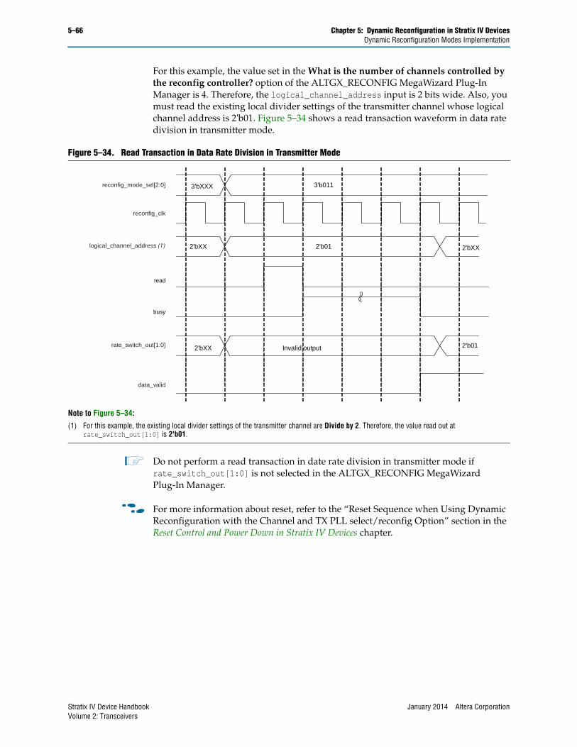
5–66 Chapter 5: Dynamic Reconfiguration in Stratix IV DevicesDynamic Reconfiguration Modes Implementation
For this example, the value set in the What is the number of channels controlled by the reconfig controller? option of the ALTGX_RECONFIG MegaWizard Plug-In Manager is 4. Therefore, the logical_channel_address input is 2 bits wide. Also, you must read the existing local divider settings of the transmitter channel whose logical channel address is 2'b01. Figure 5–34 shows a read transaction waveform in data rate division in transmitter mode.
1 Do not perform a read transaction in date rate division in transmitter mode if rate_switch_out[1:0] is not selected in the ALTGX_RECONFIG MegaWizard Plug-In Manager.
f For more information about reset, refer to the “Reset Sequence when Using Dynamic Reconfiguration with the Channel and TX PLL select/reconfig Option” section in the Reset Control and Power Down in Stratix IV Devices chapter.
Figure 5–34. Read Transaction in Data Rate Division in Transmitter Mode
Note to Figure 5–34:
(1) For this example, the existing local divider settings of the transmitter channel are Divide by 2. Therefore, the value read out at rate_switch_out[1:0] is 2'b01.
read
busy
2'bXX 2'b01
2'bXX Invalid output 2'b01
2'bXX
3'b0113'bXXXreconfig_mode_sel[2:0]
reconfig_clk
logical_channel_address (1)
rate_switch_out[1:0]
data_valid
Stratix IV Device Handbook January 2014 Altera CorporationVolume 2: Transceivers
Chapter 5: Dynamic Reconfiguration in Stratix IV Devices 5–67Dynamic Reconfiguration Modes Implementation
Offset Cancellation FeatureThe Stratix IV GX and GT devices provide an offset cancellation circuit per receiver channel to counter the offset variations due to process, voltage, and temperature (PVT). These variations create an offset in the analog circuit voltages, pushing them out of the expected range. In addition to reconfiguring the transceiver channel, the dynamic reconfiguration controller performs offset cancellation on all receiver channels connected to it on power up.
The Offset cancellation for Receiver channels option is automatically enabled in both the ALTGX and ALTGX_RECONFIG MegaWizard Plug-In Managers for Receiver and Transmitter and Receiver only configurations. It is not available for Transmitter only configurations. For Receiver and Transmitter and Receiver only configurations, you must connect the necessary interface signals between the ALTGX_RECONFIG and ALTGX (with receiver channels) instances. For the Transmitter only configuration, the ALTGX_RECONFIG must also be connected to the ALTGX by either selecting a dynamic reconfiguration mode or instantiating a dummy Receiver only ALTGX instance in each side of the device.
Offset cancellation is automatically executed once every time the device is powered on. The control logic for offset cancellation is integrated into the dynamic reconfiguration controller. You must connect the ALTGX_RECONFIG instance to the ALTGX instances (with receiver channels) in your design. You must connect the reconfig_fromgxb, reconfig_togxb, and necessary clock signals to both the ALTGX_RECONFIG and ALTGX (with receiver channels) instances.
1 The offset cancellation control functionality remains the same for both regular transceiver channels and PMA-only channels.
OperationEvery ALTGX instance for Receiver and Transmitter or Receiver only configurations require that the Offset cancellation for Receiver channels option is enabled in the Reconfig screen of the ALTGX MegaWizard Plug-In Manager. This option is enabled by default for the above two configurations. It is disabled for the Transmitter only configuration. However, for Transmitter only, the ALTGX instance still needs to be connected to ALTGX_RECONFIG. For Transmitter only, the reconfig_from_gxb, reconfig_to_gxb, busy, and reconfig_clk signals can be enabled by selecting a dynamic reconfiguration mode. The other method to connect the ALTGX_RECONFIG for Transmitter only configuration is to instantiate a dummy Receiver only ALTGX instance in each side of the device.
Because this option is enabled by default, the ALTGX instance must be connected to an ALTGX_RECONFIG instance (dynamic reconfiguration controller). The offset cancellation controls are also enabled by default in the Reconfiguration settings screen of the ALTGX_RECONFIG instance.
You must also set the starting channel number in the What is the starting channel number? option for every ALTGX instance connected to the ALTGX_RECONFIG instance. For more information, refer to:
■ “Logical Channel Addressing of Regular Transceiver Channels” on page 5–6
■ “Logical Channel Addressing of PMA-Only Channels” on page 5–7
January 2014 Altera Corporation Stratix IV Device HandbookVolume 2: Transceivers
5–68 Chapter 5: Dynamic Reconfiguration in Stratix IV DevicesDynamic Reconfiguration Modes Implementation
■ “Logical Channel Addressing—Combination of Regular Transceiver Channels and PMA-Only Channels” on page 5–9
When the device powers up, the dynamic reconfiguration controller initiates offset cancellation on the receiver channel by disconnecting the receiver input pins from the receiver data path. It also sets the receiver CDR into a fixed set of dividers to guarantee a voltage controlled oscillator (VCO) clock rate within the range necessary to provide proper offset cancellation. Subsequently, the offset cancellation process goes through different states and culminates in the offset cancellation of the receiver buffer and receiver CDR. After offset cancellation is complete, the user divider settings are restored.
The dynamic reconfiguration controller sends and receives data to the transceiver channel through the reconfig_togxb and reconfig_fromgxb signals. You must connect these signals between the ALTGX_RECONFIG instance and the ALTGX instance. You must also set the What is the number of channels controlled by the reconfig controller? option in the Reconfiguration settings screen of the ALTGX_RECONFIG MegaWizard Plug-In Manager. For more information, refer to “Total Number of Channels Option in the ALTGX_RECONFIG Instance” on page 5–10.
The Use 'logical_channel_address' port for Analog controls reconfiguration option in the Analog controls screen of the ALTGX_RECONFIG MegaWizard Plug-In Manager is not applicable for the receiver offset cancellation process.
1 If the design does not require PMA controls reconfiguration and uses optimum logic element (LE) resources, you can connect all the ALTGX instances in the design to a single dynamic reconfiguration controller (ALTGX_RECONFIG instance).
1 The gxb_powerdown signal must not be asserted during the offset cancellation sequence.
To understand the impact on system start-up when you control all the transceiver channels using a single dynamic reconfiguration controller, refer to “PMA Controls Reconfiguration Duration” on page 5–91.
ALTGX_RECONFIG Instance Signals Transition during Offset CancellationConsider that the design has ALTGX instances with channels of both Transmitter only and Receiver only configurations. You must include the Transmitter only channels while setting the What is the starting channel number? option in the ALTGX instance and setting the What is the number of channels controlled by the reconfig controller? option in the ALTGX_RECONFIG instance for receiver offset cancellation.
■ After the device powers up, the busy signal remains low for the first reconfig_clk clock cycle.
■ The busy signal then gets asserted for the second reconfig_clk clock cycle when the dynamic reconfiguration controller initiates the offset cancellation process.
■ The de-assertion of the busy signal indicates the successful completion of the offset cancellation process.
Stratix IV Device Handbook January 2014 Altera CorporationVolume 2: Transceivers
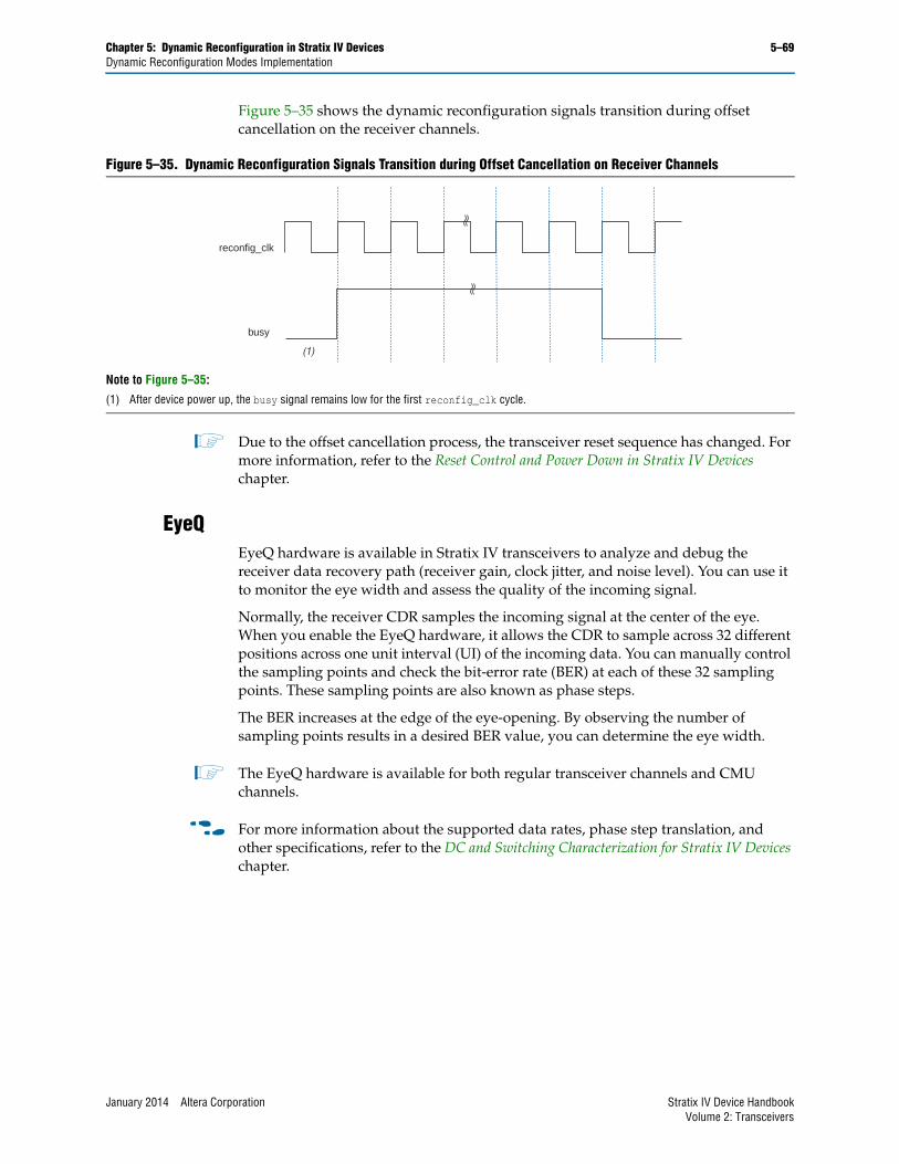
Chapter 5: Dynamic Reconfiguration in Stratix IV Devices 5–69Dynamic Reconfiguration Modes Implementation
Figure 5–35 shows the dynamic reconfiguration signals transition during offset cancellation on the receiver channels.
1 Due to the offset cancellation process, the transceiver reset sequence has changed. For more information, refer to the Reset Control and Power Down in Stratix IV Devices chapter.
EyeQEyeQ hardware is available in Stratix IV transceivers to analyze and debug the receiver data recovery path (receiver gain, clock jitter, and noise level). You can use it to monitor the eye width and assess the quality of the incoming signal.
Normally, the receiver CDR samples the incoming signal at the center of the eye. When you enable the EyeQ hardware, it allows the CDR to sample across 32 different positions across one unit interval (UI) of the incoming data. You can manually control the sampling points and check the bit-error rate (BER) at each of these 32 sampling points. These sampling points are also known as phase steps.
The BER increases at the edge of the eye-opening. By observing the number of sampling points results in a desired BER value, you can determine the eye width.
1 The EyeQ hardware is available for both regular transceiver channels and CMU channels.
f For more information about the supported data rates, phase step translation, and other specifications, refer to the DC and Switching Characterization for Stratix IV Devices chapter.
Figure 5–35. Dynamic Reconfiguration Signals Transition during Offset Cancellation on Receiver Channels
Note to Figure 5–35:
(1) After device power up, the busy signal remains low for the first reconfig_clk cycle.
reconfig_clk
busy
(1)
January 2014 Altera Corporation Stratix IV Device HandbookVolume 2: Transceivers
5–70 Chapter 5: Dynamic Reconfiguration in Stratix IV DevicesDynamic Reconfiguration Modes Implementation
Enabling the EyeQ Control Logic and the EyeQ HardwareYou must enable the EyeQ hardware in the ALTGX MegaWizard Plug-In Manager and the EyeQ control block in the ALTGX_RECONIG MegaWizard Plug-In Manager.
■ EyeQ hardware is available for each transceiver channel in the receiver data path. Select the Analog Controls option in the Reconfiguration Settings screen of the ALTGX MegaWizard Plug-In Manager to enable the EyeQ hardware.
■ EyeQ control logic is available in the dynamic reconfiguration controller. Select the EyeQ control option in the ALTGX_RECONFIG MegaWizard Plug-In Manager to enable the EyeQ control logic.
f EyeQ uses an Avalon Memory Mapped interface. For more information about this interface, refer to the Avalon Interface Specification.
Connections Between the ALTGX and ALTGX_RECONFIG InstancesTo enable the EyeQ options, follow these steps:
1. Enable the EyeQ options in the ALTGX and ALTGX_RECONFIG MegaWizard Plug-In Managers as explained in “Enabling the EyeQ Control Logic and the EyeQ Hardware” on page 5–70.
2. Connect the reconfig_{to/from}gxb ports between the ALTGX and ALTGX_RECONFIG instances.
EyeQ control logic in the dynamic reconfiguration controller allows you to write to the registers in the EyeQ hardware. Therefore, you must have a state machine in the user design that communicates to the EyeQ control block of the ALTGX_RECONFIG instance. You can then access the internal registers of the EyeQ hardware indirectly through the EyeQ control logic.
1 Altera recommends having an input pattern generator and checker to monitor the BER of the received data.
Stratix IV Device Handbook January 2014 Altera CorporationVolume 2: Transceivers
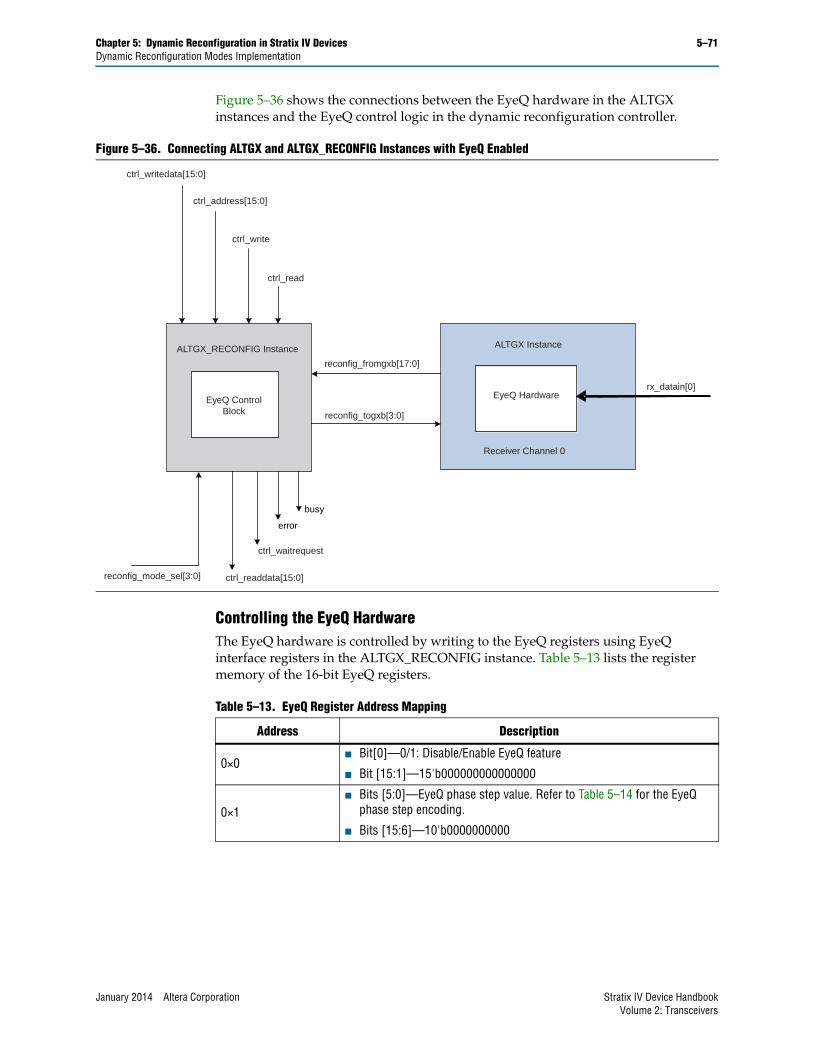
Chapter 5: Dynamic Reconfiguration in Stratix IV Devices 5–71Dynamic Reconfiguration Modes Implementation
Figure 5–36 shows the connections between the EyeQ hardware in the ALTGX instances and the EyeQ control logic in the dynamic reconfiguration controller.
Controlling the EyeQ HardwareThe EyeQ hardware is controlled by writing to the EyeQ registers using EyeQ interface registers in the ALTGX_RECONFIG instance. Table 5–13 lists the register memory of the 16-bit EyeQ registers.
Figure 5–36. Connecting ALTGX and ALTGX_RECONFIG Instances with EyeQ Enabled
busy
error
ctrl_writedata[15:0]
ctrl_address[15:0]
ctrl_write
ctrl_read
reconfig_fromgxb[17:0]
reconfig_togxb[3:0]
rx_datain[0]
ALTGX Instance
EyeQ Hardware
Receiver Channel 0
ALTGX_RECONFIG Instance
EyeQ ControlBlock
ctrl_waitrequest
ctrl_readdata[15:0]reconfig_mode_sel[3:0]
Table 5–13. EyeQ Register Address Mapping
Address Description
0×0■ Bit[0]—0/1: Disable/Enable EyeQ feature
■ Bit [15:1]—15'b000000000000000
0×1■ Bits [5:0]—EyeQ phase step value. Refer to Table 5–14 for the EyeQ
phase step encoding.
■ Bits [15:6]—10'b0000000000
January 2014 Altera Corporation Stratix IV Device HandbookVolume 2: Transceivers
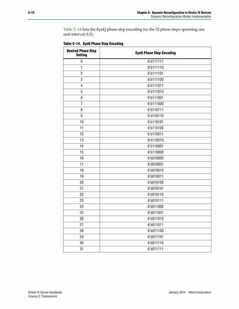
5–72 Chapter 5: Dynamic Reconfiguration in Stratix IV DevicesDynamic Reconfiguration Modes Implementation
Table 5–14 lists the EyeQ phase step encoding for the 32 phase steps spanning one unit interval (UI).
Table 5–14. EyeQ Phase Step Encoding
Desired Phase Step Setting EyeQ Phase Step Encoding
0 6'b111111
1 6'b111110
2 6'b111101
3 6'b111100
4 6'b111011
5 6'b111010
6 6'b111001
7 6'b111000
8 6'b110111
9 6'b110110
10 6'b110101
11 6'b110100
12 6'b110011
13 6'b110010
14 6'b110001
15 6'b110000
16 6'b010000
17 6'b010001
18 6'b010010
19 6'b010011
20 6'b010100
21 6'b010101
22 6'b010110
23 6'b010111
24 6'b011000
25 6'b011001
26 6'b011010
27 6'b011011
28 6'b011100
29 6'b011101
30 6'b011110
31 6'b011111
Stratix IV Device Handbook January 2014 Altera CorporationVolume 2: Transceivers
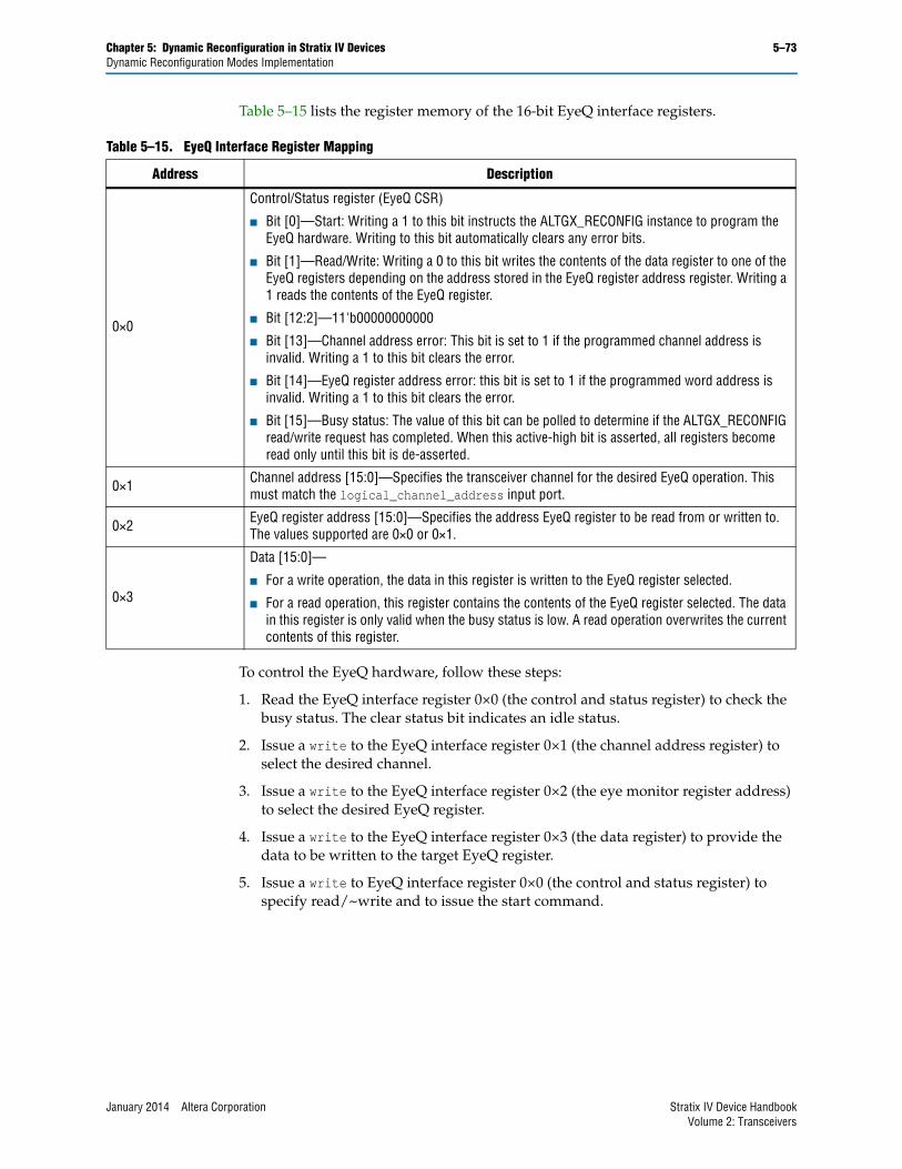
Chapter 5: Dynamic Reconfiguration in Stratix IV Devices 5–73Dynamic Reconfiguration Modes Implementation
Table 5–15 lists the register memory of the 16-bit EyeQ interface registers.
To control the EyeQ hardware, follow these steps:
1. Read the EyeQ interface register 0×0 (the control and status register) to check the busy status. The clear status bit indicates an idle status.
2. Issue a write to the EyeQ interface register 0×1 (the channel address register) to select the desired channel.
3. Issue a write to the EyeQ interface register 0×2 (the eye monitor register address) to select the desired EyeQ register.
4. Issue a write to the EyeQ interface register 0×3 (the data register) to provide the data to be written to the target EyeQ register.
5. Issue a write to EyeQ interface register 0×0 (the control and status register) to specify read/~write and to issue the start command.
Table 5–15. EyeQ Interface Register Mapping
Address Description
0×0
Control/Status register (EyeQ CSR)
■ Bit [0]—Start: Writing a 1 to this bit instructs the ALTGX_RECONFIG instance to program the EyeQ hardware. Writing to this bit automatically clears any error bits.
■ Bit [1]—Read/Write: Writing a 0 to this bit writes the contents of the data register to one of the EyeQ registers depending on the address stored in the EyeQ register address register. Writing a 1 reads the contents of the EyeQ register.
■ Bit [12:2]—11'b00000000000
■ Bit [13]—Channel address error: This bit is set to 1 if the programmed channel address is invalid. Writing a 1 to this bit clears the error.
■ Bit [14]—EyeQ register address error: this bit is set to 1 if the programmed word address is invalid. Writing a 1 to this bit clears the error.
■ Bit [15]—Busy status: The value of this bit can be polled to determine if the ALTGX_RECONFIG read/write request has completed. When this active-high bit is asserted, all registers become read only until this bit is de-asserted.
0×1 Channel address [15:0]—Specifies the transceiver channel for the desired EyeQ operation. This must match the logical_channel_address input port.
0×2 EyeQ register address [15:0]—Specifies the address EyeQ register to be read from or written to. The values supported are 0×0 or 0×1.
0×3
Data [15:0]—
■ For a write operation, the data in this register is written to the EyeQ register selected.
■ For a read operation, this register contains the contents of the EyeQ register selected. The data in this register is only valid when the busy status is low. A read operation overwrites the current contents of this register.
January 2014 Altera Corporation Stratix IV Device HandbookVolume 2: Transceivers
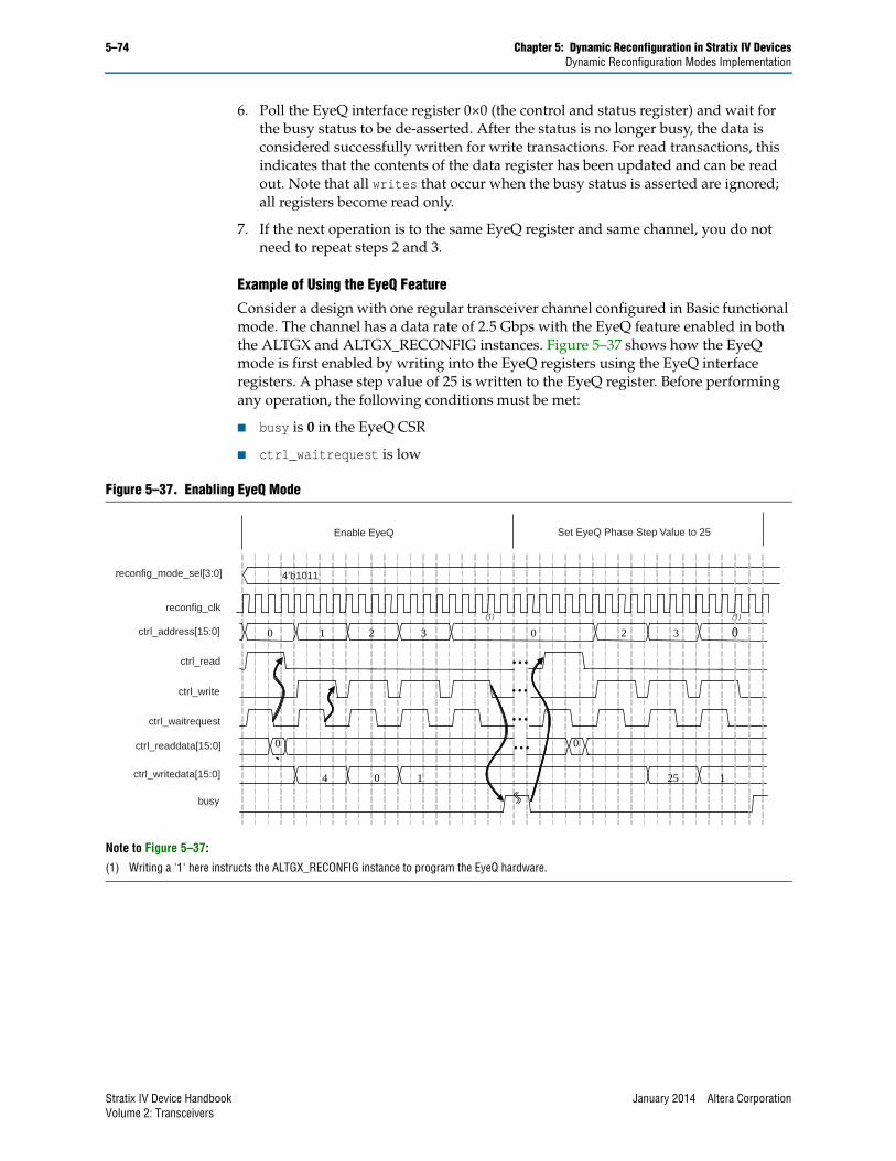
5–74 Chapter 5: Dynamic Reconfiguration in Stratix IV DevicesDynamic Reconfiguration Modes Implementation
6. Poll the EyeQ interface register 0×0 (the control and status register) and wait for the busy status to be de-asserted. After the status is no longer busy, the data is considered successfully written for write transactions. For read transactions, this indicates that the contents of the data register has been updated and can be read out. Note that all writes that occur when the busy status is asserted are ignored; all registers become read only.
7. If the next operation is to the same EyeQ register and same channel, you do not need to repeat steps 2 and 3.
Example of Using the EyeQ Feature
Consider a design with one regular transceiver channel configured in Basic functional mode. The channel has a data rate of 2.5 Gbps with the EyeQ feature enabled in both the ALTGX and ALTGX_RECONFIG instances. Figure 5–37 shows how the EyeQ mode is first enabled by writing into the EyeQ registers using the EyeQ interface registers. A phase step value of 25 is written to the EyeQ register. Before performing any operation, the following conditions must be met:
■ busy is 0 in the EyeQ CSR
■ ctrl_waitrequest is low
Figure 5–37. Enabling EyeQ Mode
Note to Figure 5–37:
(1) Writing a '1' here instructs the ALTGX_RECONFIG instance to program the EyeQ hardware.
0
x0
…
…
…
…
4 0 1 25 1
0 1 2 3 0 2 3 0
reconfig_mode_sel[3:0]
reconfig_clk
ctrl_address[15:0]
ctrl_read
ctrl_write
ctrl_waitrequest
ctrl_readdata[15:0]
ctrl_writedata[15:0]
busy
Enable EyeQ Set EyeQ Phase Step Value to 25
4’b1011
(1)(1)
Stratix IV Device Handbook January 2014 Altera CorporationVolume 2: Transceivers
Chapter 5: Dynamic Reconfiguration in Stratix IV Devices 5–75Dynamic Reconfiguration Modes Implementation
Adaptive Equalization (AEQ)High-speed interface systems require different equalization settings to compensate for changing data rates and backplane losses. Manual tuning of the receiver channel’s equalization stages involves finding the optimal settings through trial and error, and then locking in those values at compile time. This manual method is cumbersome under varying system characteristics. The AEQ feature solves this problem by automatically tuning an active receiver channel’s equalization filters based on a frequency content comparison between the incoming signal and internally generated reference signals.
User logic can dynamically control the AEQ hardware in the receiver through the dynamic reconfiguration controller. This section describes how to enable different options and use them to control the AEQ hardware.
Adaptive Equalization LimitationsThe following are the AEQ feature requirements and limitations:
■ The receive data must be 8B/10B encoded
■ Not available in PCIe functional mode (because the AEQ hardware cannot perform the equalization process when the receive link is under the electrical idle condition)
■ The receiver input signal must have a minimum envelope of 400 mv (differential peak-to-peak). The Quartus II software does not check for this requirement
■ The AEQ hardware is not present in the CMU channels
f For more information about speed grade, data rates, receiver input signal level, and other specifications that support the AEQ feature, refer to the DC and Switching Characterization for Stratix IV Devices chapter.
Enabling the AEQ Control Logic and AEQ HardwareTo use the AEQ feature, enable the AEQ hardware in the ALTGX MegaWizard Plug-In Manager and the AEQ control block in the ALTGX_RECONIG MegaWizard Plug-In Manager. To enable the AEQ hardware and the AEQ control logic:
■ Select the Enable adaptive equalizer control option in the Reconfiguration Settings screen of the ALTGX MegaWizard Plug-In Manager. The AEQ hardware is available for each transceiver channel in the receiver data path.
■ Select the Enable adaptive equalizer control option in the ALTGX_RECONFIG MegaWizard Plug-In Manager. The AEQ control logic is available in the dynamic reconfiguration controller.
When you select the above two options, the ALTGX and ALTGX_RECONFIG MegaWizard Plug-In Managers provide the following additional ports:
■ aeq_fromgxb[]
■ aeq_togxb[]
The aeq_fromgxb[] and aeq_togxb[] ports provide the interface between the receiver channel and the dynamic reconfiguration controller.
January 2014 Altera Corporation Stratix IV Device HandbookVolume 2: Transceivers
5–76 Chapter 5: Dynamic Reconfiguration in Stratix IV DevicesDynamic Reconfiguration Modes Implementation
The following section describes the connections between the AEQ control block of the ALTGX_RECONFIG instance and the AEQ hardware of the ALTGX instance.
Connections Between the ALTGX and ALTGX_RECONFIG InstancesEnable the adaptive equalization options in the ALTGX and ALTGX_RECONFIG MegaWizard Plug-In Managers, as explained in the previous section. To use the AEQ control block and AEQ hardware, you must connect the ALTGX receivers to the ALTGX_RECONFIG instance using the reconfig_{to/from}gxb and aeq_{to/from}gxb ports. You must also connect the ALTGX_RECONFIG instance to your design.
If you have multiple transceiver instances and a single ALTGX_RECONFIG instance, connect the LSB of the aeq_togxb[] and aeq_fromgxb[] ports of the ALTGX_RECONFIG instance to the transceiver channel with a logical_channel_address value of 0.
Stratix IV Device Handbook January 2014 Altera CorporationVolume 2: Transceivers
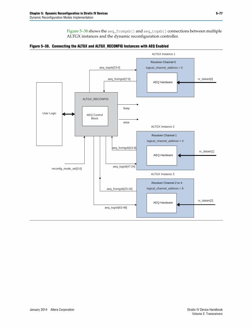
Chapter 5: Dynamic Reconfiguration in Stratix IV Devices 5–77Dynamic Reconfiguration Modes Implementation
Figure 5–38 shows the aeq_fromgxb[] and aeq_togxb[] connections between multiple ALTGX instances and the dynamic reconfiguration controller.
Figure 5–38. Connecting the ALTGX and ALTGX_RECONFIG Instances with AEQ Enabled
Receiver Channel 0
AEQ Hardware
busy
error
User Logic
ALTGX Instance 1
aeq_togxb[23:0]
aeq_fromgxb[7:0]
logical_channel_address = 0
rx_datain[0]
ALTGX Instance 2
Receiver Channel 1
logical_channel_address = 4
AEQ Hardwarerx_datain[1]
ALTGX_RECONFIG
AEQ ControlBlock
aeq_fromgxb[15:8]
aeq_togxb[47:24]reconfig_mode_sel[3:0]
ALTGX Instance 3
Receiver Channel 2 to 4
logical_channel_address = 8
AEQ Hardware
aeq_fromgxb[23:16]
aeq_togxb[63:48]
rx_datain[2]
January 2014 Altera Corporation Stratix IV Device HandbookVolume 2: Transceivers
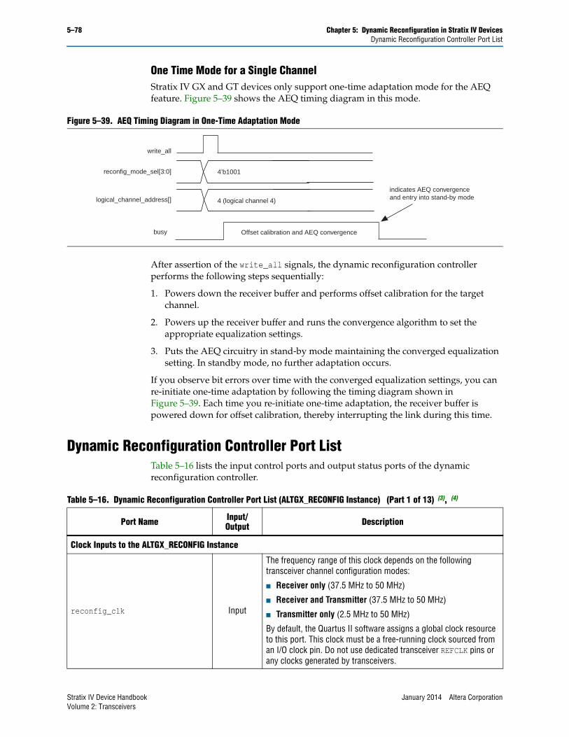
5–78 Chapter 5: Dynamic Reconfiguration in Stratix IV DevicesDynamic Reconfiguration Controller Port List
One Time Mode for a Single ChannelStratix IV GX and GT devices only support one-time adaptation mode for the AEQ feature. Figure 5–39 shows the AEQ timing diagram in this mode.
After assertion of the write_all signals, the dynamic reconfiguration controller performs the following steps sequentially:
1. Powers down the receiver buffer and performs offset calibration for the target channel.
2. Powers up the receiver buffer and runs the convergence algorithm to set the appropriate equalization settings.
3. Puts the AEQ circuitry in stand-by mode maintaining the converged equalization setting. In standby mode, no further adaptation occurs.
If you observe bit errors over time with the converged equalization settings, you can re-initiate one-time adaptation by following the timing diagram shown in Figure 5–39. Each time you re-initiate one-time adaptation, the receiver buffer is powered down for offset calibration, thereby interrupting the link during this time.
Dynamic Reconfiguration Controller Port ListTable 5–16 lists the input control ports and output status ports of the dynamic reconfiguration controller.
Figure 5–39. AEQ Timing Diagram in One-Time Adaptation Mode
write_all
reconfig_mode_sel[3:0]
logical_channel_address[]
busy
4 (logical channel 4)
4’b1001
indicates AEQ convergenceand entry into stand-by mode
Offset calibration and AEQ convergence
Table 5–16. Dynamic Reconfiguration Controller Port List (ALTGX_RECONFIG Instance) (Part 1 of 13) (3), (4)
Port Name Input/Output Description
Clock Inputs to the ALTGX_RECONFIG Instance
reconfig_clk Input
The frequency range of this clock depends on the following transceiver channel configuration modes:
■ Receiver only (37.5 MHz to 50 MHz)
■ Receiver and Transmitter (37.5 MHz to 50 MHz)
■ Transmitter only (2.5 MHz to 50 MHz)
By default, the Quartus II software assigns a global clock resource to this port. This clock must be a free-running clock sourced from an I/O clock pin. Do not use dedicated transceiver REFCLK pins or any clocks generated by transceivers.
Stratix IV Device Handbook January 2014 Altera CorporationVolume 2: Transceivers
Chapter 5: Dynamic Reconfiguration in Stratix IV Devices 5–79Dynamic Reconfiguration Controller Port List
ALTGX and ALTGX_RECONFIG Interface Signals
reconfig_fromgxb Input
An output port in the ALTGX instance and an input port in the ALTGX_RECONFIG instance. This signal is transceiver-block based. Therefore, the width of this signal increases in steps of 17 bits per transceiver block.
In the ALTGX MegaWizard Plug-In Manager, the width of this signal depends on the following:
■ Whether the channels configured in the ALTGX instance are regular transceiver channels or PMA-only channels.
■ The number of channels you select in the What is the number of channels? option in the General screen.
For example, if the channels in the ALTGX instance are regular transceiver channels and if you select the number of channels as follows:
1 Channels 4, then the output port reconfig_fromgxb = 17 bits
5 Channels 8, then the output port reconfig_fromgxb = 34 bits
9 Channels 12, then the output port reconfig_fromgxb = 51 bits
However, if the channels in the ALTGX instance are PMA-only channels and if you select the number of channels as follows:
Number of PMA-only channels = n, then the output port reconfig_fromgxb = n*17 bits
For example, reconfig_fromgxb = 6 * 17 bits for 6 PMA-only channels.
In the ALTGX_RECONFIG MegaWizard Plug-In Manager, the width of this signal depends on the value you select in the What is the number of channels controlled by the reconfig controller? option in the Reconfiguration settings screen.
For example, if you select the total number of channels controlled by ALTGX_RECONFIG instance as follows:
1 Channels 4, then the input port reconfig_fromgxb = 17 bits
5 Channels 8, then the input port reconfig_fromgxb = 34 bits
9 Channels 12, then the input port reconfig_fromgxb = 51 bits
Table 5–16. Dynamic Reconfiguration Controller Port List (ALTGX_RECONFIG Instance) (Part 2 of 13) (3), (4)
Port Name Input/Output Description
January 2014 Altera Corporation Stratix IV Device HandbookVolume 2: Transceivers
5–80 Chapter 5: Dynamic Reconfiguration in Stratix IV DevicesDynamic Reconfiguration Controller Port List
reconfig_fromgxb
(continued)Input
To connect the reconfig_fromgxb port between the ALTGX_RECONFIG instance and multiple ALTGX instances, follow these rules:
■ Connect the reconfig_fromgxb[16:0] of ALTGX Instance 1 to the reconfig_fromgxb[16:0] of the ALTGX_RECONFIG instance. Connect the reconfig_fromgxb[] port of the next ALTGX instance to the next available bits of the ALTGX_RECONFIG instance, and so on.
■ Connect the reconfig_fromgxb port of the ALTGX instance, which has the highest What is the starting channel number? option, to the MSB of the reconfig_fromgxb port of the ALTGX_RECONFIG instance.
The Quartus II Fitter produces an error if the dynamic reconfiguration option is enabled in the ALTGX instance but the reconfig_fromgxb and reconfig_togxb ports are not connected to the ALTGX_RECONFIG instance.
For more information, refer to “Connecting the ALTGX and ALTGX_RECONFIG Instances” on page 5–11.
reconfig_togxb[3:0] Output
An input port of the ALTGX instance and an output port of the ALTGX_RECONFIG instance. You must connect the reconfig_togxb[3:0] input port of every ALTGX instance controlled by the dynamic reconfiguration controller to the reconfig_togxb[3:0] output port of the ALTGX_RECONFIG instance.
The width of this port is always fixed to 3 bits.
For more information, refer to “Connecting the ALTGX and ALTGX_RECONFIG Instances” on page 5–11.
FPGA Fabric and ALTGX_RECONFIG Interface Signals
write_all Input
Assert this signal for one reconfig_clk clock cycle to initiate a write transaction from the ALTGX_RECONFIG instance to the ALTGX instance.
You can use this signal in two ways for .mif-based modes:
■ Continuous write operation—Select the Enable continuous write of all the words needed for reconfiguration option to pulse the write_all signal only once for writing a whole .mif. The What is the read latency of the MIF contents option is available for selection in this case only. Enter the desired latency in terms of the reconfig_clk cycles.
■ Regular write operation—When the Enable continuous write of all the words needed for reconfiguration option is disabled, every word of the .mif requires its own write cycle.
Table 5–16. Dynamic Reconfiguration Controller Port List (ALTGX_RECONFIG Instance) (Part 3 of 13) (3), (4)
Port Name Input/Output Description
Stratix IV Device Handbook January 2014 Altera CorporationVolume 2: Transceivers
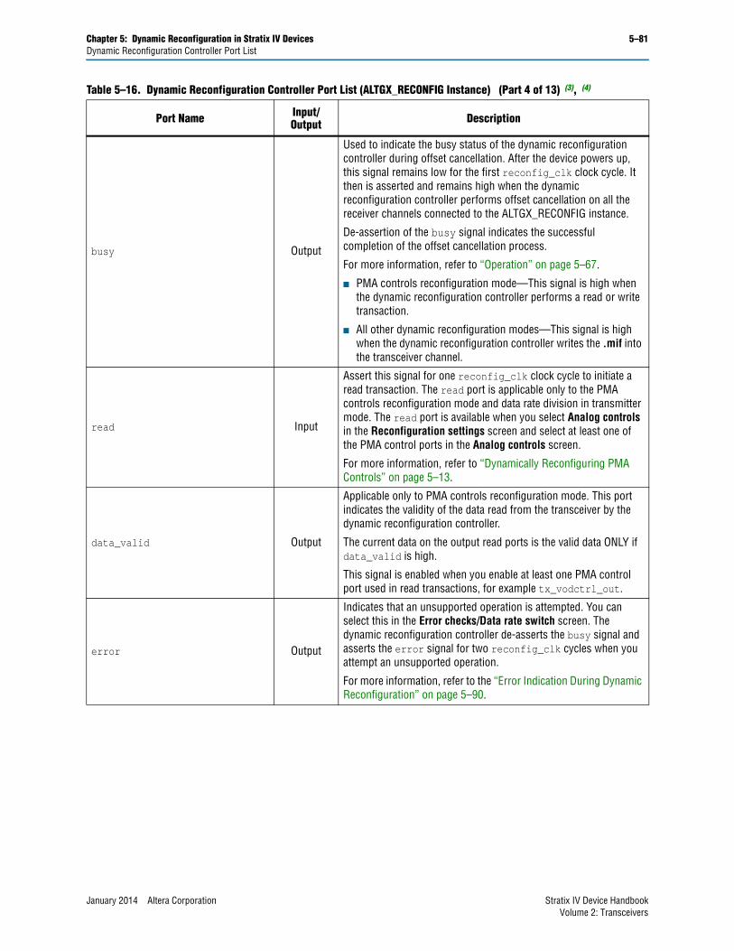
Chapter 5: Dynamic Reconfiguration in Stratix IV Devices 5–81Dynamic Reconfiguration Controller Port List
busy Output
Used to indicate the busy status of the dynamic reconfiguration controller during offset cancellation. After the device powers up, this signal remains low for the first reconfig_clk clock cycle. It then is asserted and remains high when the dynamic reconfiguration controller performs offset cancellation on all the receiver channels connected to the ALTGX_RECONFIG instance.
De-assertion of the busy signal indicates the successful completion of the offset cancellation process.
For more information, refer to “Operation” on page 5–67.
■ PMA controls reconfiguration mode—This signal is high when the dynamic reconfiguration controller performs a read or write transaction.
■ All other dynamic reconfiguration modes—This signal is high when the dynamic reconfiguration controller writes the .mif into the transceiver channel.
read Input
Assert this signal for one reconfig_clk clock cycle to initiate a read transaction. The read port is applicable only to the PMA controls reconfiguration mode and data rate division in transmitter mode. The read port is available when you select Analog controls in the Reconfiguration settings screen and select at least one of the PMA control ports in the Analog controls screen.
For more information, refer to “Dynamically Reconfiguring PMA Controls” on page 5–13.
data_valid Output
Applicable only to PMA controls reconfiguration mode. This port indicates the validity of the data read from the transceiver by the dynamic reconfiguration controller.
The current data on the output read ports is the valid data ONLY if data_valid is high.
This signal is enabled when you enable at least one PMA control port used in read transactions, for example tx_vodctrl_out.
error Output
Indicates that an unsupported operation is attempted. You can select this in the Error checks/Data rate switch screen. The dynamic reconfiguration controller de-asserts the busy signal and asserts the error signal for two reconfig_clk cycles when you attempt an unsupported operation.
For more information, refer to the “Error Indication During Dynamic Reconfiguration” on page 5–90.
Table 5–16. Dynamic Reconfiguration Controller Port List (ALTGX_RECONFIG Instance) (Part 4 of 13) (3), (4)
Port Name Input/Output Description
January 2014 Altera Corporation Stratix IV Device HandbookVolume 2: Transceivers
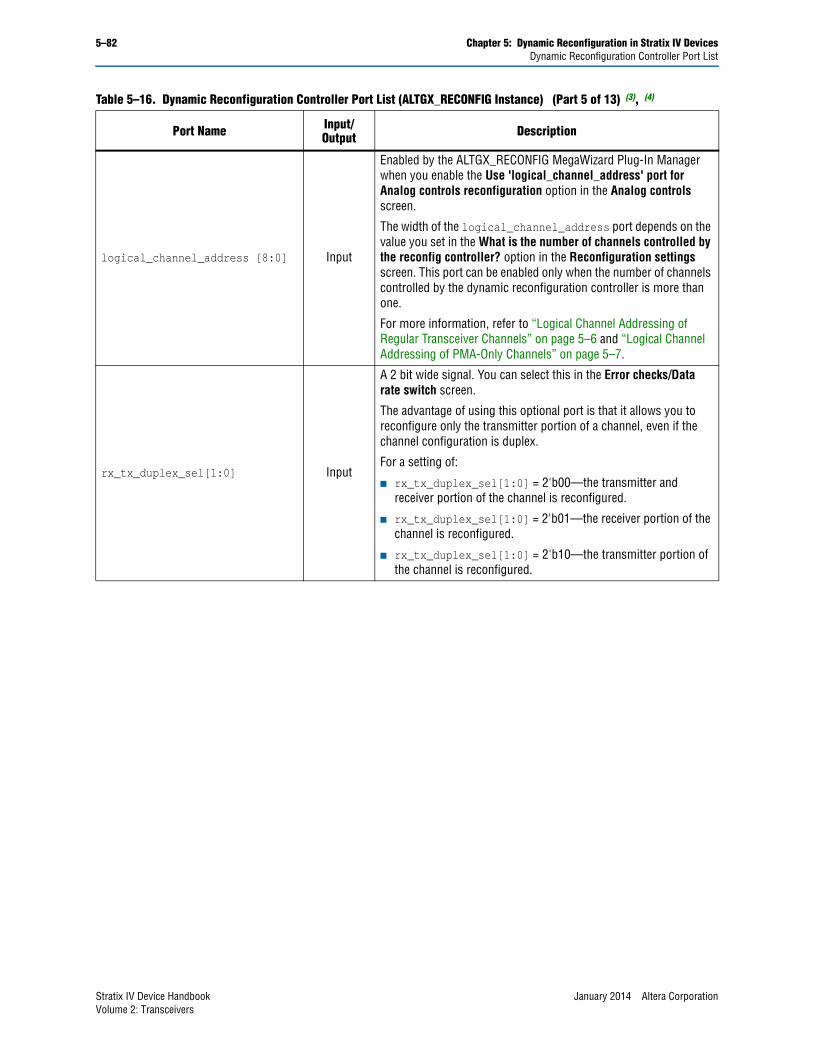
5–82 Chapter 5: Dynamic Reconfiguration in Stratix IV DevicesDynamic Reconfiguration Controller Port List
logical_channel_address [8:0] Input
Enabled by the ALTGX_RECONFIG MegaWizard Plug-In Manager when you enable the Use 'logical_channel_address' port for Analog controls reconfiguration option in the Analog controls screen.
The width of the logical_channel_address port depends on the value you set in the What is the number of channels controlled by the reconfig controller? option in the Reconfiguration settings screen. This port can be enabled only when the number of channels controlled by the dynamic reconfiguration controller is more than one.
For more information, refer to “Logical Channel Addressing of Regular Transceiver Channels” on page 5–6 and “Logical Channel Addressing of PMA-Only Channels” on page 5–7.
rx_tx_duplex_sel[1:0] Input
A 2 bit wide signal. You can select this in the Error checks/Data rate switch screen.
The advantage of using this optional port is that it allows you to reconfigure only the transmitter portion of a channel, even if the channel configuration is duplex.
For a setting of:
■ rx_tx_duplex_sel[1:0] = 2'b00—the transmitter and receiver portion of the channel is reconfigured.
■ rx_tx_duplex_sel[1:0] = 2'b01—the receiver portion of the channel is reconfigured.
■ rx_tx_duplex_sel[1:0] = 2'b10—the transmitter portion of the channel is reconfigured.
Table 5–16. Dynamic Reconfiguration Controller Port List (ALTGX_RECONFIG Instance) (Part 5 of 13) (3), (4)
Port Name Input/Output Description
Stratix IV Device Handbook January 2014 Altera CorporationVolume 2: Transceivers
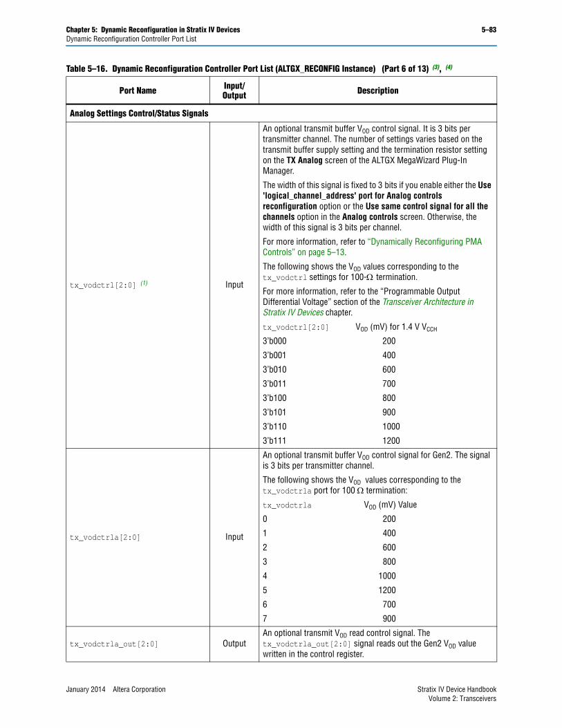
Chapter 5: Dynamic Reconfiguration in Stratix IV Devices 5–83Dynamic Reconfiguration Controller Port List
Analog Settings Control/Status Signals
tx_vodctrl[2:0] (1) Input
An optional transmit buffer VOD control signal. It is 3 bits per transmitter channel. The number of settings varies based on the transmit buffer supply setting and the termination resistor setting on the TX Analog screen of the ALTGX MegaWizard Plug-In Manager.
The width of this signal is fixed to 3 bits if you enable either the Use 'logical_channel_address' port for Analog controls reconfiguration option or the Use same control signal for all the channels option in the Analog controls screen. Otherwise, the width of this signal is 3 bits per channel.
For more information, refer to “Dynamically Reconfiguring PMA Controls” on page 5–13.
The following shows the VOD values corresponding to the tx_vodctrl settings for 100- termination.
For more information, refer to the “Programmable Output Differential Voltage” section of the Transceiver Architecture in Stratix IV Devices chapter.
tx_vodctrl[2:0] VOD (mV) for 1.4 V VCCH
3’b000 200
3’b001 400
3’b010 600
3’b011 700
3’b100 800
3’b101 900
3’b110 1000
3’b111 1200
tx_vodctrla[2:0] Input
An optional transmit buffer VOD control signal for Gen2. The signal is 3 bits per transmitter channel.
The following shows the VOD values corresponding to the tx_vodctrla port for 100 termination:
tx_vodctrla VOD (mV) Value
0 200
1 400
2 600
3 800
4 1000
5 1200
6 700
7 900
tx_vodctrla_out[2:0] OutputAn optional transmit VOD read control signal. The tx_vodctrla_out[2:0] signal reads out the Gen2 VOD value written in the control register.
Table 5–16. Dynamic Reconfiguration Controller Port List (ALTGX_RECONFIG Instance) (Part 6 of 13) (3), (4)
Port Name Input/Output Description
January 2014 Altera Corporation Stratix IV Device HandbookVolume 2: Transceivers
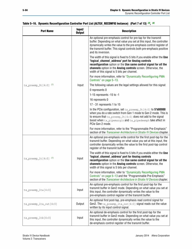
5–84 Chapter 5: Dynamic Reconfiguration in Stratix IV DevicesDynamic Reconfiguration Controller Port List
tx_preemp_0t[4:0] (1) Input
An optional pre-emphasis control for pre-tap for the transmit buffer. Depending on what value you set at this input, the controller dynamically writes the value to the pre-emphasis control register of the transmit buffer. This signal controls both pre-emphasis positive and its inversion.
The width of this signal is fixed to 5 bits if you enable either the Use 'logical_channel_address' port for Analog controls reconfiguration option or the Use same control signal for all the channels option in the Analog controls screen. Otherwise, the width of this signal is 5 bits per channel.
For more information, refer to “Dynamically Reconfiguring PMA Controls” on page 5–13.
The following values are the legal settings allowed for this signal:
0 represents 0
1-15 represents -15 to -1
16 represents 0
17 - 31 represents 1 to 15
In the PCIe configuration, set tx_preemp_0t[4:0] to 5'b00000 when you do a rate switch from Gen 1 mode to Gen 2 mode. This is to ensure that tx_preemp_0t[4:0] does not add to the signal boost when tx_pipemargin and tx_pipedeemph take affect in PCIe Gen 2 mode.
For more information, refer to the “Programmable Pre-Emphasis” section of the Transceiver Architecture in Stratix IV Devices chapter.
tx_preemp_1t[4:0] (1) Input
An optional pre-emphasis write control for the first post-tap for the transmit buffer. Depending on what value you set at this input, the controller dynamically writes the value to the first post-tap control register of the transmit buffer.
The width of this signal is fixed to 5 bits if you enable either the Use 'logical_channel_address' port for Analog controls reconfiguration option or the Use same control signal for all the channels option in the Analog controls screen. Otherwise, the width of this signal is 5 bits per channel.
For more information, refer to “Dynamically Reconfiguring PMA Controls” on page 5–13 and the “Programmable Pre-Emphasis” section of the Transceiver Architecture in Stratix IV Devices chapter.
tx_preemp_1ta[4:0] Input
An optional pre-emphasis control for the first post-tap for the transmit buffer in Gen2 mode. Depending on what value you set at this input, the controller dynamically writes the value to the pre-emphasis control register of the transmit buffer.
tx_preemp_1ta_out[4:0] OutputAn optional first post-tap, pre-emphasis read control signal for Gen2. The tx_preemp_1ta_out[4:0] signal reads out the value written by its input control signal.
tx_preemp_1tb[4:0] Input
An optional de-emphasis control for the first post-tap for the transmit buffer in Gen2 mode. Depending on what value you set at this input, the controller dynamically writes the value to the de-emphasis control register of the transmit buffer.
Table 5–16. Dynamic Reconfiguration Controller Port List (ALTGX_RECONFIG Instance) (Part 7 of 13) (3), (4)
Port Name Input/Output Description
Stratix IV Device Handbook January 2014 Altera CorporationVolume 2: Transceivers
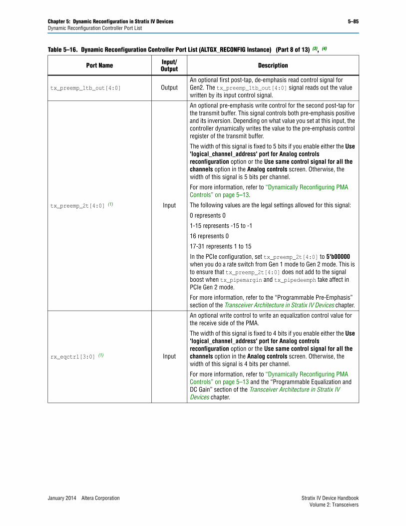
Chapter 5: Dynamic Reconfiguration in Stratix IV Devices 5–85Dynamic Reconfiguration Controller Port List
tx_preemp_1tb_out[4:0] OutputAn optional first post-tap, de-emphasis read control signal for Gen2. The tx_preemp_1tb_out[4:0] signal reads out the value written by its input control signal.
tx_preemp_2t[4:0] (1) Input
An optional pre-emphasis write control for the second post-tap for the transmit buffer. This signal controls both pre-emphasis positive and its inversion. Depending on what value you set at this input, the controller dynamically writes the value to the pre-emphasis control register of the transmit buffer.
The width of this signal is fixed to 5 bits if you enable either the Use 'logical_channel_address' port for Analog controls reconfiguration option or the Use same control signal for all the channels option in the Analog controls screen. Otherwise, the width of this signal is 5 bits per channel.
For more information, refer to “Dynamically Reconfiguring PMA Controls” on page 5–13.
The following values are the legal settings allowed for this signal:
0 represents 0
1-15 represents -15 to -1
16 represents 0
17-31 represents 1 to 15
In the PCIe configuration, set tx_preemp_2t[4:0] to 5'b00000 when you do a rate switch from Gen 1 mode to Gen 2 mode. This is to ensure that tx_preemp_2t[4:0] does not add to the signal boost when tx_pipemargin and tx_pipedeemph take affect in PCIe Gen 2 mode.
For more information, refer to the “Programmable Pre-Emphasis” section of the Transceiver Architecture in Stratix IV Devices chapter.
rx_eqctrl[3:0] (1) Input
An optional write control to write an equalization control value for the receive side of the PMA.
The width of this signal is fixed to 4 bits if you enable either the Use 'logical_channel_address' port for Analog controls reconfiguration option or the Use same control signal for all the channels option in the Analog controls screen. Otherwise, the width of this signal is 4 bits per channel.
For more information, refer to “Dynamically Reconfiguring PMA Controls” on page 5–13 and the “Programmable Equalization and DC Gain” section of the Transceiver Architecture in Stratix IV Devices chapter.
Table 5–16. Dynamic Reconfiguration Controller Port List (ALTGX_RECONFIG Instance) (Part 8 of 13) (3), (4)
Port Name Input/Output Description
January 2014 Altera Corporation Stratix IV Device HandbookVolume 2: Transceivers
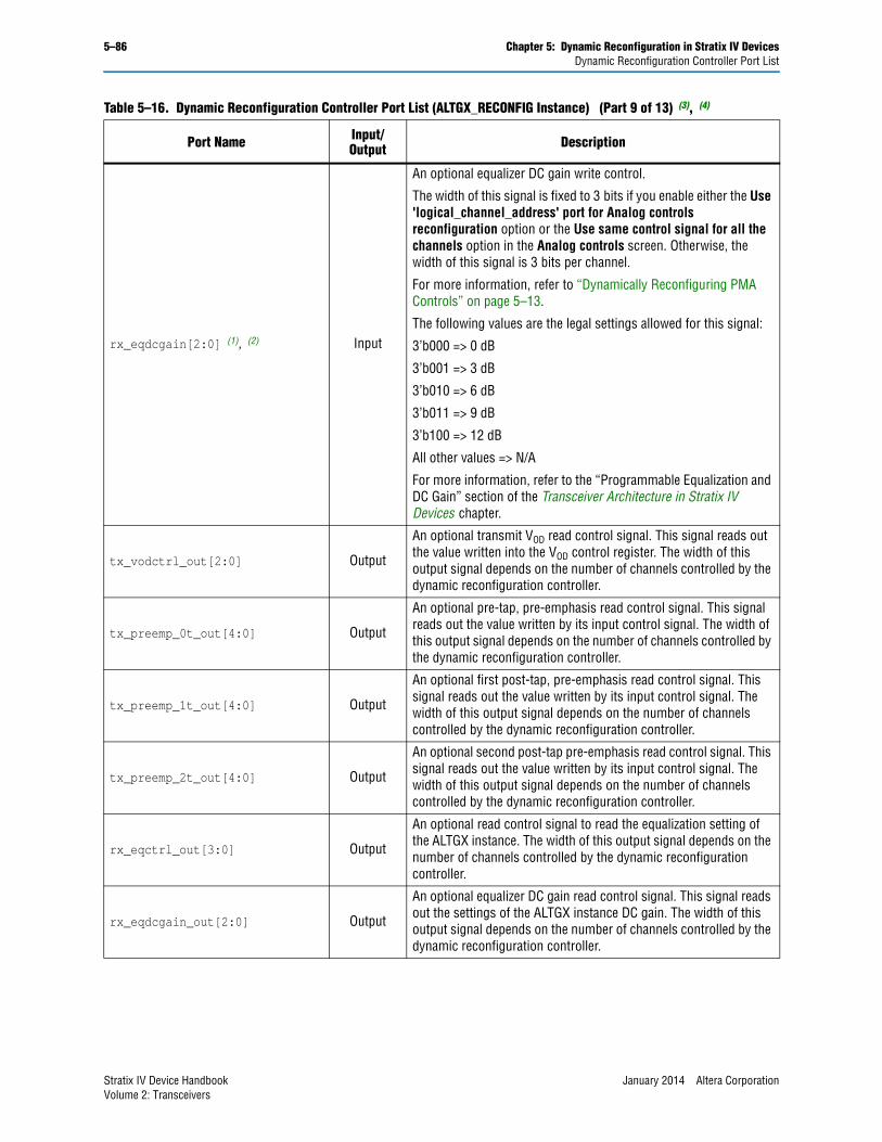
5–86 Chapter 5: Dynamic Reconfiguration in Stratix IV DevicesDynamic Reconfiguration Controller Port List
rx_eqdcgain[2:0] (1), (2) Input
An optional equalizer DC gain write control.
The width of this signal is fixed to 3 bits if you enable either the Use 'logical_channel_address' port for Analog controls reconfiguration option or the Use same control signal for all the channels option in the Analog controls screen. Otherwise, the width of this signal is 3 bits per channel.
For more information, refer to “Dynamically Reconfiguring PMA Controls” on page 5–13.
The following values are the legal settings allowed for this signal:
3’b000 => 0 dB
3’b001 => 3 dB
3’b010 => 6 dB
3’b011 => 9 dB
3’b100 => 12 dB
All other values => N/A
For more information, refer to the “Programmable Equalization and DC Gain” section of the Transceiver Architecture in Stratix IV Devices chapter.
tx_vodctrl_out[2:0] Output
An optional transmit VOD read control signal. This signal reads out the value written into the VOD control register. The width of this output signal depends on the number of channels controlled by the dynamic reconfiguration controller.
tx_preemp_0t_out[4:0] Output
An optional pre-tap, pre-emphasis read control signal. This signal reads out the value written by its input control signal. The width of this output signal depends on the number of channels controlled by the dynamic reconfiguration controller.
tx_preemp_1t_out[4:0] Output
An optional first post-tap, pre-emphasis read control signal. This signal reads out the value written by its input control signal. The width of this output signal depends on the number of channels controlled by the dynamic reconfiguration controller.
tx_preemp_2t_out[4:0] Output
An optional second post-tap pre-emphasis read control signal. This signal reads out the value written by its input control signal. The width of this output signal depends on the number of channels controlled by the dynamic reconfiguration controller.
rx_eqctrl_out[3:0] Output
An optional read control signal to read the equalization setting of the ALTGX instance. The width of this output signal depends on the number of channels controlled by the dynamic reconfiguration controller.
rx_eqdcgain_out[2:0] Output
An optional equalizer DC gain read control signal. This signal reads out the settings of the ALTGX instance DC gain. The width of this output signal depends on the number of channels controlled by the dynamic reconfiguration controller.
Table 5–16. Dynamic Reconfiguration Controller Port List (ALTGX_RECONFIG Instance) (Part 9 of 13) (3), (4)
Port Name Input/Output Description
Stratix IV Device Handbook January 2014 Altera CorporationVolume 2: Transceivers
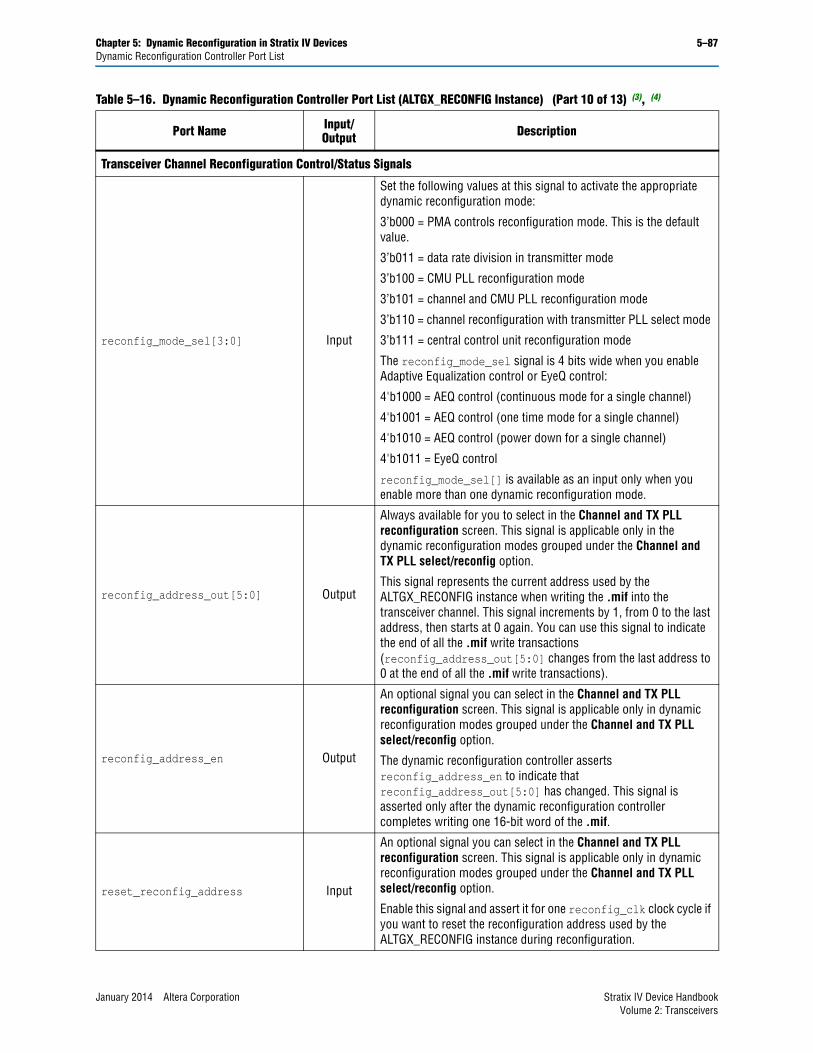
Chapter 5: Dynamic Reconfiguration in Stratix IV Devices 5–87Dynamic Reconfiguration Controller Port List
Transceiver Channel Reconfiguration Control/Status Signals
reconfig_mode_sel[3:0] Input
Set the following values at this signal to activate the appropriate dynamic reconfiguration mode:
3’b000 = PMA controls reconfiguration mode. This is the default value.
3’b011 = data rate division in transmitter mode
3’b100 = CMU PLL reconfiguration mode
3’b101 = channel and CMU PLL reconfiguration mode
3’b110 = channel reconfiguration with transmitter PLL select mode
3’b111 = central control unit reconfiguration mode
The reconfig_mode_sel signal is 4 bits wide when you enable Adaptive Equalization control or EyeQ control:
4'b1000 = AEQ control (continuous mode for a single channel)
4'b1001 = AEQ control (one time mode for a single channel)
4'b1010 = AEQ control (power down for a single channel)
4'b1011 = EyeQ control
reconfig_mode_sel[] is available as an input only when you enable more than one dynamic reconfiguration mode.
reconfig_address_out[5:0] Output
Always available for you to select in the Channel and TX PLL reconfiguration screen. This signal is applicable only in the dynamic reconfiguration modes grouped under the Channel and TX PLL select/reconfig option.
This signal represents the current address used by the ALTGX_RECONFIG instance when writing the .mif into the transceiver channel. This signal increments by 1, from 0 to the last address, then starts at 0 again. You can use this signal to indicate the end of all the .mif write transactions (reconfig_address_out[5:0] changes from the last address to 0 at the end of all the .mif write transactions).
reconfig_address_en Output
An optional signal you can select in the Channel and TX PLL reconfiguration screen. This signal is applicable only in dynamic reconfiguration modes grouped under the Channel and TX PLL select/reconfig option.
The dynamic reconfiguration controller asserts reconfig_address_en to indicate that reconfig_address_out[5:0] has changed. This signal is asserted only after the dynamic reconfiguration controller completes writing one 16-bit word of the .mif.
reset_reconfig_address Input
An optional signal you can select in the Channel and TX PLL reconfiguration screen. This signal is applicable only in dynamic reconfiguration modes grouped under the Channel and TX PLL select/reconfig option.
Enable this signal and assert it for one reconfig_clk clock cycle if you want to reset the reconfiguration address used by the ALTGX_RECONFIG instance during reconfiguration.
Table 5–16. Dynamic Reconfiguration Controller Port List (ALTGX_RECONFIG Instance) (Part 10 of 13) (3), (4)
Port Name Input/Output Description
January 2014 Altera Corporation Stratix IV Device HandbookVolume 2: Transceivers
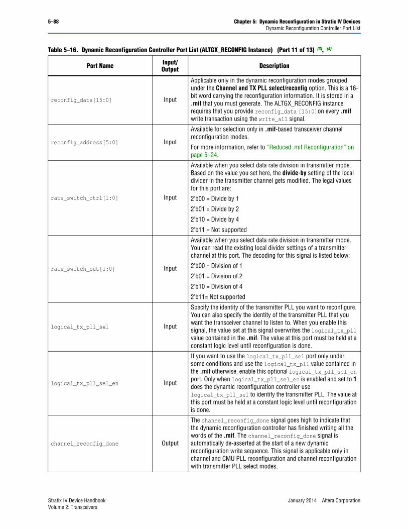
5–88 Chapter 5: Dynamic Reconfiguration in Stratix IV DevicesDynamic Reconfiguration Controller Port List
reconfig_data[15:0] Input
Applicable only in the dynamic reconfiguration modes grouped under the Channel and TX PLL select/reconfig option. This is a 16-bit word carrying the reconfiguration information. It is stored in a .mif that you must generate. The ALTGX_RECONFIG instance requires that you provide reconfig_data [15:0]on every .mif write transaction using the write_all signal.
reconfig_address[5:0] Input
Available for selection only in .mif-based transceiver channel reconfiguration modes.
For more information, refer to “Reduced .mif Reconfiguration” on page 5–24.
rate_switch_ctrl[1:0] Input
Available when you select data rate division in transmitter mode. Based on the value you set here, the divide-by setting of the local divider in the transmitter channel gets modified. The legal values for this port are:
2’b00 = Divide by 1
2’b01 = Divide by 2
2’b10 = Divide by 4
2’b11 = Not supported
rate_switch_out[1:0] Input
Available when you select data rate division in transmitter mode. You can read the existing local divider settings of a transmitter channel at this port. The decoding for this signal is listed below:
2’b00 = Division of 1
2’b01 = Division of 2
2’b10 = Division of 4
2’b11= Not supported
logical_tx_pll_sel Input
Specify the identity of the transmitter PLL you want to reconfigure. You can also specify the identity of the transmitter PLL that you want the transceiver channel to listen to. When you enable this signal, the value set at this signal overwrites the logical_tx_pll value contained in the .mif. The value at this port must be held at a constant logic level until reconfiguration is done.
logical_tx_pll_sel_en Input
If you want to use the logical_tx_pll_sel port only under some conditions and use the logical_tx_pll value contained in the .mif otherwise, enable this optional logical_tx_pll_sel_en port. Only when logical_tx_pll_sel_en is enabled and set to 1 does the dynamic reconfiguration controller use logical_tx_pll_sel to identify the transmitter PLL. The value at this port must be held at a constant logic level until reconfiguration is done.
channel_reconfig_done Output
The channel_reconfig_done signal goes high to indicate that the dynamic reconfiguration controller has finished writing all the words of the .mif. The channel_reconfig_done signal is automatically de-asserted at the start of a new dynamic reconfiguration write sequence. This signal is applicable only in channel and CMU PLL reconfiguration and channel reconfiguration with transmitter PLL select modes.
Table 5–16. Dynamic Reconfiguration Controller Port List (ALTGX_RECONFIG Instance) (Part 11 of 13) (3), (4)
Port Name Input/Output Description
Stratix IV Device Handbook January 2014 Altera CorporationVolume 2: Transceivers
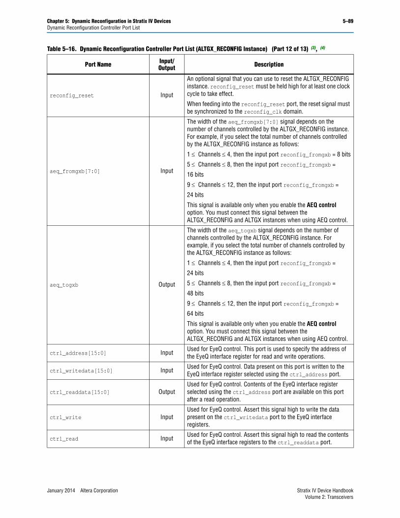
Chapter 5: Dynamic Reconfiguration in Stratix IV Devices 5–89Dynamic Reconfiguration Controller Port List
reconfig_reset Input
An optional signal that you can use to reset the ALTGX_RECONFIG instance. reconfig_reset must be held high for at least one clock cycle to take effect.
When feeding into the reconfig_reset port, the reset signal must be synchronized to the reconfig_clk domain.
aeq_fromgxb[7:0] Input
The width of the aeq_fromgxb[7:0] signal depends on the number of channels controlled by the ALTGX_RECONFIG instance. For example, if you select the total number of channels controlled by the ALTGX_RECONFIG instance as follows:
1 Channels 4, then the input port reconfig_fromgxb = 8 bits
5 Channels 8, then the input port reconfig_fromgxb =
16 bits
9 Channels 12, then the input port reconfig_fromgxb =
24 bits
This signal is available only when you enable the AEQ control option. You must connect this signal between the ALTGX_RECONFIG and ALTGX instances when using AEQ control.
aeq_togxb Output
The width of the aeq_togxb signal depends on the number of channels controlled by the ALTGX_RECONFIG instance. For example, if you select the total number of channels controlled by the ALTGX_RECONFIG instance as follows:
1 Channels 4, then the input port reconfig_fromgxb =
24 bits
5 Channels 8, then the input port reconfig_fromgxb =
48 bits
9 Channels 12, then the input port reconfig_fromgxb =
64 bits
This signal is available only when you enable the AEQ control option. You must connect this signal between the ALTGX_RECONFIG and ALTGX instances when using AEQ control.
ctrl_address[15:0] Input Used for EyeQ control. This port is used to specify the address of the EyeQ interface register for read and write operations.
ctrl_writedata[15:0] Input Used for EyeQ control. Data present on this port is written to the EyeQ interface register selected using the ctrl_address port.
ctrl_readdata[15:0] OutputUsed for EyeQ control. Contents of the EyeQ interface register selected using the ctrl_address port are available on this port after a read operation.
ctrl_write InputUsed for EyeQ control. Assert this signal high to write the data present on the ctrl_writedata port to the EyeQ interface registers.
ctrl_read Input Used for EyeQ control. Assert this signal high to read the contents of the EyeQ interface registers to the ctrl_readdata port.
Table 5–16. Dynamic Reconfiguration Controller Port List (ALTGX_RECONFIG Instance) (Part 12 of 13) (3), (4)
Port Name Input/Output Description
January 2014 Altera Corporation Stratix IV Device HandbookVolume 2: Transceivers
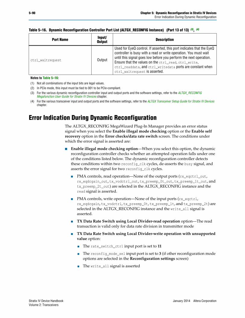
5–90 Chapter 5: Dynamic Reconfiguration in Stratix IV DevicesError Indication During Dynamic Reconfiguration
Error Indication During Dynamic ReconfigurationThe ALTGX_RECONFIG MegaWizard Plug-In Manager provides an error status signal when you select the Enable illegal mode checking option or the Enable self recovery option in the Error checks/data rate switch screen. The conditions under which the error signal is asserted are:
■ Enable illegal mode checking option—When you select this option, the dynamic reconfiguration controller checks whether an attempted operation falls under one of the conditions listed below. The dynamic reconfiguration controller detects these conditions within two reconfig_clk cycles, de-asserts the busy signal, and asserts the error signal for two reconfig_clk cycles.
■ PMA controls, read operation—None of the output ports (rx_eqctrl_out, rx_eqdcgain_out, tx_vodctrl_out, tx_preemp_0t_out, tx_preemp_1t_out, and tx_preemp_2t_out) are selected in the ALTGX_RECONFIG instance and the read signal is asserted.
■ PMA controls, write operation—None of the input ports (rx_eqctrl, rx_eqdcgain, tx_vodctrl, tx_preemp_0t, tx_preemp_1t, and tx_preemp_2t) are selected in the ALTGX_RECONFIG instance and the write_all signal is asserted.
■ TX Data Rate Switch using Local Divider-read operation option—The read transaction is valid only for data rate division in transmitter mode
■ TX Data Rate Switch using Local Divider-write operation with unsupported value option:
■ The rate_switch_ctrl input port is set to 11
■ The reconfig_mode_sel input port is set to 3 (if other reconfiguration mode options are selected in the Reconfiguration settings screen)
■ The write_all signal is asserted
ctrl_waitrequest Output
Used for EyeQ control. If asserted, this port indicates that the EyeQ controller is busy with a read or write operation. You must wait until this signal goes low before you perform the next operation. Ensure that the values on the ctrl_read, ctrl_write, ctrl_readdata, and ctrl_writedata ports are constant when ctrl_waitrequest is asserted.
Notes to Table 5–16:
(1) Not all combinations of the input bits are legal values. (2) In PCIe mode, this input must be tied to 001 to be PCIe-compliant.(3) For the various dynamic reconfiguration controller input and output ports and the software settings, refer to the ALTGX_RECONFIG
Megafunction User Guide for Stratix IV Devices chapter.(4) For the various transceiver input and output ports and the software settings, refer to the ALTGX Transceiver Setup Guide for Stratix IV Devices
chapter.
Table 5–16. Dynamic Reconfiguration Controller Port List (ALTGX_RECONFIG Instance) (Part 13 of 13) (3), (4)
Port Name Input/Output Description
Stratix IV Device Handbook January 2014 Altera CorporationVolume 2: Transceivers
Chapter 5: Dynamic Reconfiguration in Stratix IV Devices 5–91Dynamic Reconfiguration Duration
■ TX Data Rate Switch using Local Divider-write operation without input port option:
■ The rate_switch_ctrl input port is not used
■ The reconfig_mode_sel port is set to 3 (if other reconfiguration mode options are selected in the Reconfiguration settings screen)
■ The write_all signal is asserted
■ TX Data Rate Switch using Local Divider- read operation without output port option:
■ The rate_switch_out output port is not used
■ The reconfig_mode_sel port is set to 3 (if other reconfiguration mode options are selected in the Reconfiguration settings screen)
■ The read signal is asserted
■ Channel and/or TX PLL reconfig/select-read operation option:
■ The reconfig_mode_sel input port is set to 4, 5, 6, or 7
■ The read signal is asserted
■ Adaptive Equalization option—read operation:
■ The reconfig_mode_sel input port is set to 7, 8, 9, or 10
■ The read signal is asserted
■ EyeQ option—read operation:
■ The reconfig_mode_sel input port is set to 11
■ The read signal is asserted
■ Enable self recovery option—When you select this option, the controller automatically recovers if the operation did not complete within the expected time. The error signal is driven high whenever the controller performs a self recovery.
Dynamic Reconfiguration DurationDynamic reconfiguration duration is the number of cycles the busy signal is asserted when the dynamic reconfiguration controller performs write transactions, read transactions, or offset cancellation of the receiver channels.
PMA Controls Reconfiguration DurationThe following section contains an estimate of the number of reconfig_clk clock cycles the busy signal is asserted during PMA controls reconfiguration using Method 1, Method 2, or Method 3. For more information, refer to “Dynamically Reconfiguring PMA Controls” on page 5–13.
January 2014 Altera Corporation Stratix IV Device HandbookVolume 2: Transceivers
5–92 Chapter 5: Dynamic Reconfiguration in Stratix IV DevicesDynamic Reconfiguration Duration
PMA Controls Reconfiguration Duration When Using Method 1
The logical_channel_address port is used in Method 1. The write transaction and read transaction duration is as follows:
Write Transaction Duration
For writing values to the following PMA controls, the busy signal is asserted for 260 reconfig_clk clock cycles for each of these controls:
■ tx_preemp_1t (pre-emphasis control first post-tap)
■ tx_vodctrl (voltage output differential)
■ rx_eqctrl (equalizer control)
■ rx_eqdcgain (equalizer DC gain)
For writing values to the following PMA controls, the busy signal is asserted for 520 reconfig_clk clock cycles for each of these controls:
■ tx_preemp_0t (pre-emphasis control pre-tap)
■ tx_preemp_2t (pre-emphasis control second post-tap)
Read Transaction Duration
For reading the existing values of the following PMA controls, the busy signal is asserted for 130 reconfig_clk clock cycles for each of these controls. The data_valid signal is then asserted after the busy signal goes low.
■ tx_preemp_1t_out (pre-emphasis control first post-tap)
■ tx_vodctrl_out (voltage output differential)
■ rx_eqctrl_out (equalizer control)
■ rx_eqdcgain_out (equalizer DC gain)
For reading the existing values of the following PMA controls, the busy signal is asserted for 260 reconfig_clk clock cycles for each of these controls. The data_valid signal is then asserted after the busy signal goes low.
■ tx_preemp_0t_out (pre-emphasis control pre-tap)
■ tx_preemp_2t_out (pre-emphasis control second post-tap)
PMA Controls Reconfiguration Duration When Using Method 2 or Method 3
The logical_channel_address port is not used in Method 2 and Method 3. The write transaction duration and read transaction duration are as follows:
Write Transaction Duration
For writing values to the following PMA controls, the busy signal is asserted for 260 reconfig_clk clock cycles per channel for each of these controls:
■ tx_preemp_1t (pre-emphasis control first post-tap)
■ tx_vodctrl (voltage output differential)
■ rx_eqctrl (equalizer control)
■ rx_eqdcgain (equalizer DC gain)
Stratix IV Device Handbook January 2014 Altera CorporationVolume 2: Transceivers
Chapter 5: Dynamic Reconfiguration in Stratix IV Devices 5–93Dynamic Reconfiguration Duration
For writing values to the following PMA controls, the busy signal is asserted for 520 reconfig_clk clock cycles per channel for each of these controls:
■ tx_preemp_0t (pre-emphasis control pre-tap)
■ tx_preemp_2t (pre-emphasis control second post-tap)
Read Transaction Duration
For reading the existing values of the following PMA controls, the busy signal is asserted for 130 reconfig_clk clock cycles per channel for each of these controls. The data_valid signal is then asserted after the busy signal goes low.
■ tx_preemp_1t_out (pre-emphasis control first post-tap)
■ tx_vodctrl_out (voltage output differential)
■ rx_eqctrl_out (equalizer control)
■ rx_eqdcgain_out (equalizer DC gain)
For reading the existing values of the following PMA controls, the busy signal is asserted for 260 reconfig_clk clock cycles per channel for each of these controls. The data_valid signal is then asserted after the busy signal goes low.
■ tx_preemp_0t_out (pre-emphasis control pre-tap)
■ tx_preemp_2t_out (pre-emphasis control second post-tap)
Offset Cancellation DurationWhen the device powers up, the busy signal remains low for the first reconfig_clk clock cycle. Offset cancellation control is only for the receiver channels. The ALTGX_RECONFIG instance takes 18500 reconfig_clk clock cycles per channel for Receiver only and Receiver and Transmitter channels. It takes 900 reconfig_clk clock cycles per channel for Transmitter only channels to determine if the channel under reconfiguration is a receiver channel or not. The ATLGX_RECONFIG requires an additional 130,000 clock cycles for these values to take effect. The ALTGX_RECONFIG instance takes approximately two reconfig_clk clock cycles per channel for the unused logical channels.
To demonstrate offset cancellation duration, consider the following example:
■ One ALTGX_RECONFIG instance is connected to two ALTGX instances.
■ ALTGX Instance 1 has one Transmitter only channel (logical_channel_address = 0)
■ ALTGX Instance 2 has one Receiver only channel (logical_channel_address = 4)
For this example, the ALTGX_RECONFIG instance consumes the following number of reconfig_clk clock cycles for offset cancellation:
■ 900 cycles for the Transmitter only channel
■ 18,500 cycles for the Receiver only channel
■ 2 cycles each for non-existent channels with logical_channel_addresses = 1, 2, and 3 and 130,000 cycles as a baseline for the values to take affect.
The offset cancellation duration for the ALTGX_RECONFIG instance to reconfigure the Transmitter only channel, Receiver only channel, non-existent logical channels 1, 2, and 3 = 149,406 cycles (900 +18,500 +6 + 130,000).
January 2014 Altera Corporation Stratix IV Device HandbookVolume 2: Transceivers
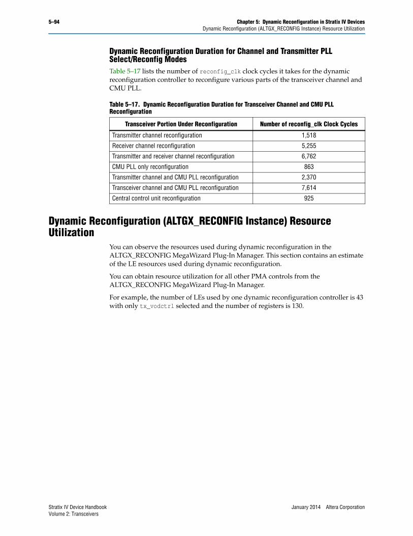
5–94 Chapter 5: Dynamic Reconfiguration in Stratix IV DevicesDynamic Reconfiguration (ALTGX_RECONFIG Instance) Resource Utilization
Dynamic Reconfiguration Duration for Channel and Transmitter PLL Select/Reconfig ModesTable 5–17 lists the number of reconfig_clk clock cycles it takes for the dynamic reconfiguration controller to reconfigure various parts of the transceiver channel and CMU PLL.
Dynamic Reconfiguration (ALTGX_RECONFIG Instance) Resource Utilization
You can observe the resources used during dynamic reconfiguration in the ALTGX_RECONFIG MegaWizard Plug-In Manager. This section contains an estimate of the LE resources used during dynamic reconfiguration.
You can obtain resource utilization for all other PMA controls from the ALTGX_RECONFIG MegaWizard Plug-In Manager.
For example, the number of LEs used by one dynamic reconfiguration controller is 43 with only tx_vodctrl selected and the number of registers is 130.
Table 5–17. Dynamic Reconfiguration Duration for Transceiver Channel and CMU PLL Reconfiguration
Transceiver Portion Under Reconfiguration Number of reconfig_clk Clock Cycles
Transmitter channel reconfiguration 1,518
Receiver channel reconfiguration 5,255
Transmitter and receiver channel reconfiguration 6,762
CMU PLL only reconfiguration 863
Transmitter channel and CMU PLL reconfiguration 2,370
Transceiver channel and CMU PLL reconfiguration 7,614
Central control unit reconfiguration 925
Stratix IV Device Handbook January 2014 Altera CorporationVolume 2: Transceivers
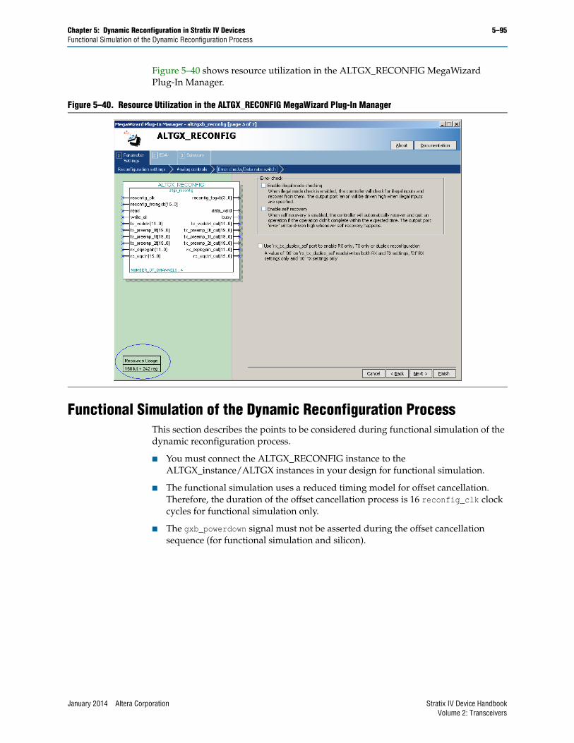
Chapter 5: Dynamic Reconfiguration in Stratix IV Devices 5–95Functional Simulation of the Dynamic Reconfiguration Process
Figure 5–40 shows resource utilization in the ALTGX_RECONFIG MegaWizard Plug-In Manager.
Functional Simulation of the Dynamic Reconfiguration ProcessThis section describes the points to be considered during functional simulation of the dynamic reconfiguration process.
■ You must connect the ALTGX_RECONFIG instance to the ALTGX_instance/ALTGX instances in your design for functional simulation.
■ The functional simulation uses a reduced timing model for offset cancellation. Therefore, the duration of the offset cancellation process is 16 reconfig_clk clock cycles for functional simulation only.
■ The gxb_powerdown signal must not be asserted during the offset cancellation sequence (for functional simulation and silicon).
Figure 5–40. Resource Utilization in the ALTGX_RECONFIG MegaWizard Plug-In Manager
January 2014 Altera Corporation Stratix IV Device HandbookVolume 2: Transceivers
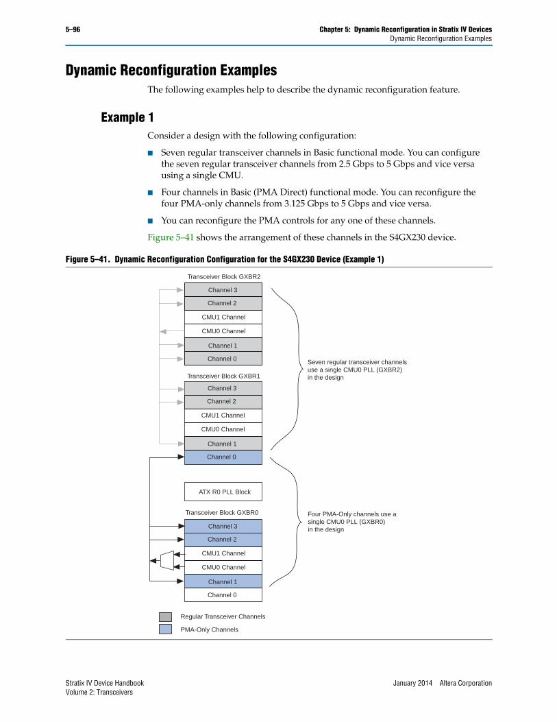
5–96 Chapter 5: Dynamic Reconfiguration in Stratix IV DevicesDynamic Reconfiguration Examples
Dynamic Reconfiguration ExamplesThe following examples help to describe the dynamic reconfiguration feature.
Example 1Consider a design with the following configuration:
■ Seven regular transceiver channels in Basic functional mode. You can configure the seven regular transceiver channels from 2.5 Gbps to 5 Gbps and vice versa using a single CMU.
■ Four channels in Basic (PMA Direct) functional mode. You can reconfigure the four PMA-only channels from 3.125 Gbps to 5 Gbps and vice versa.
■ You can reconfigure the PMA controls for any one of these channels.
Figure 5–41 shows the arrangement of these channels in the S4GX230 device.
Figure 5–41. Dynamic Reconfiguration Configuration for the S4GX230 Device (Example 1)
Transceiver Block GXBR2
Channel 3
Channel 2
CMU1 Channel
CMU0 Channel
Channel 1
Channel 0
Transceiver Block GXBR1
Channel 3
Channel 2
CMU1 Channel
CMU0 Channel
Channel 1
Channel 0
ATX R0 PLL Block
Transceiver Block GXBR0
Channel 3
Channel 2
CMU1 Channel
CMU0 Channel
Channel 1
Channel 0
Regular Transceiver Channels
PMA-Only Channels
Four PMA-Only channels use asingle CMU0 PLL (GXBR0)in the design
Seven regular transceiver channels use a single CMU0 PLL (GXBR2)in the design
Stratix IV Device Handbook January 2014 Altera CorporationVolume 2: Transceivers
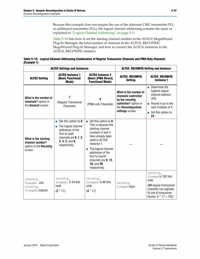
Chapter 5: Dynamic Reconfiguration in Stratix IV Devices 5–97Dynamic Reconfiguration Examples
Because this example does not require the use of the alternate CMU transmitter PLL or additional transmitter PLLs, the logical channel addressing remains the same as explained in “Logical Channel Addressing” on page 5–5.
Table 5–18 lists how to set the starting channel number in the ALTGX MegaWizard Plug-In Manager, the total number of channels in the ALTGX_RECONFIG MegaWizard Plug-In Manager, and how to connect the ALTGX instances to the ALTGX_RECONFIG instance.
Table 5–18. Logical Channel Addressing Combination of Regular Transceiver Channels and PMA-Only Channels (Example 1)
ALTGX Settings and Instances ALTGX_RECONFIG Setting and Instance
ALTGX SettingALTGX Instance 1 (Basic Functional
Mode)
ALTGX Instance 2 (Basic [PMA Direct] Functional Mode)
ALTGX_RECONFIG Setting
ALTGX_RECONFIG Instance 1
What is the number of channels? option in the General screen
7
(Regular Transceiver Channels)
4
(PMA-only Channels)
What is the number of channels controlled by the reconfig controller? option in the Reconfiguration settings screen.
■ Determine the highest logical channel address (20).
■ Round it up to the next multiple of 4.
■ Set this option to 24.
What is the starting channel number? option in the Reconfig screen
■ Set this option to 0.
■ The logical channel addresses of the first to sixth channels are 0, 1, 2, 3, 4, 5, and 6, respectively.
■ Set this option to 8. This is because the starting channel numbers 0 and 4 have already been used in ALTGX instance 1.
■ The logical channel addresses of the first to fourth channels are 8, 12, 16, and 20, respectively.
— —
reconfig_fromgxb1 and reconfig_fromgxb2 outputs
reconfig_fromgxb1 is 34 bits wide
(2 * 17)
reconfig_fromgxb2 is 68 bits wide
(4 * 17)
reconfig_fromgxb input
reconfig_fromgxb is 102 bits wide
(24 regular transceiver channels can logically fit into 6 transceiver blocks; 6 * 17 = 102)
January 2014 Altera Corporation Stratix IV Device HandbookVolume 2: Transceivers
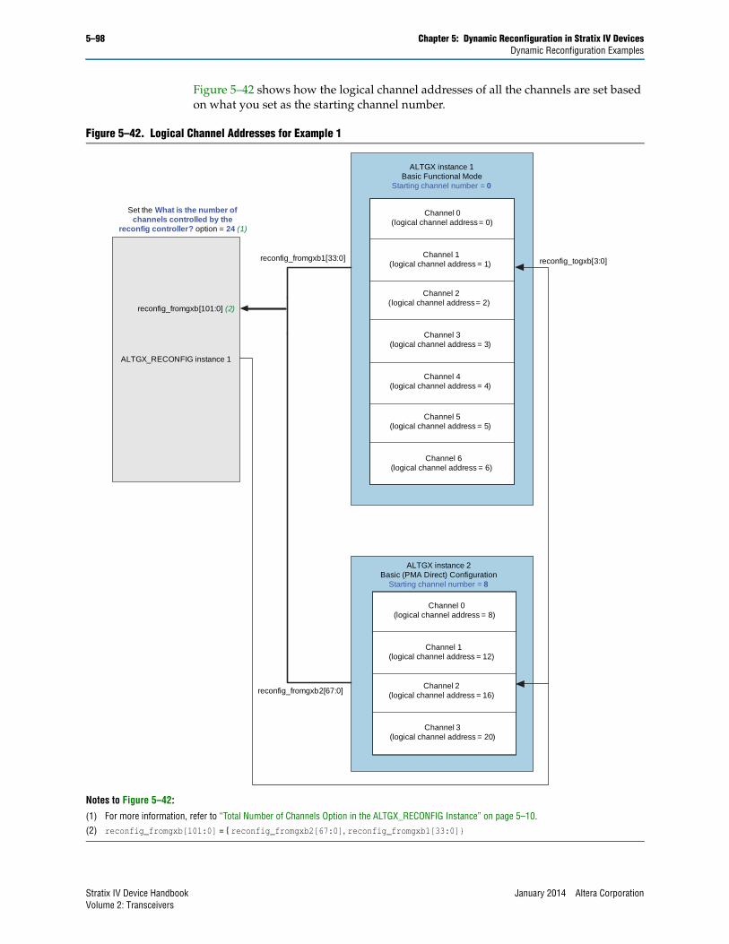
5–98 Chapter 5: Dynamic Reconfiguration in Stratix IV DevicesDynamic Reconfiguration Examples
Figure 5–42 shows how the logical channel addresses of all the channels are set based on what you set as the starting channel number.
Figure 5–42. Logical Channel Addresses for Example 1
Notes to Figure 5–42:
(1) For more information, refer to “Total Number of Channels Option in the ALTGX_RECONFIG Instance” on page 5–10.(2) reconfig_fromgxb[101:0] = { reconfig_fromgxb2[67:0], reconfig_fromgxb1[33:0]}
ALTGX instance 1 Basic Functional Mode
Starting channel number = 0
ALTGX_RECONFIG instance 1
Set the What is the number of channels controlled by the
reconfig controller? option = 24 (1)
ALTGX instance 2Basic (PMA Direct) Configuration
Starting channel number = 8
reconfig_fromgxb1[33:0]
reconfig_fromgxb2[67:0]
reconfig_fromgxb[101:0] (2)
reconfig_togxb[3:0]
Channel 0 (logical channel address = 0)
Channel 1 (logical channel address = 1)
Channel 2 (logical channel address = 2)
Channel 3 (logical channel address = 3)
Channel 4 (logical channel address = 4)
Channel 5 (logical channel address = 5)
Channel 6 (logical channel address = 6)
Channel 0 (logical channel address = 8)
Channel 1 (logical channel address = 12)
Channel 2 (logical channel address = 16)
Channel 3 (logical channel address = 20)
Stratix IV Device Handbook January 2014 Altera CorporationVolume 2: Transceivers
Chapter 5: Dynamic Reconfiguration in Stratix IV Devices 5–99Dynamic Reconfiguration Examples
Different Dynamic Reconfiguration Modes Involved
1. Channel and CMU PLL reconfiguration mode:
■ is used for reconfiguring the seven regular transceiver channels from one data rate to another using the same CMU0 PLL (in GXBR2)
1 This mode is chosen because both the receiver and transmitter of the regular channels must be re-configured using a single CMU.
2. Channel and CMU PLL select reconfiguration mode:
■ is used for reconfiguring the four PMA-only channels from one data rate to another using the CMU0 PLL (in GXBR0) and CMU1 PLL (GXBR0)
1 This mode is chosen because both the receiver and transmitter of the regular channels must be re-configured and more than one CMU can be used.
3. The rx_tx_duplex_sel[1:0] port allows you to reconfigure the transmitter and receiver channels to operate at the different data rates.
4. PMA controls reconfiguration mode used to configure the PMA settings for all the channels.
For more information, refer to “Transceiver Channel Reconfiguration Mode Details” on page 5–19.
.mif Generation
The following .mifs are required for this example:
■ For the seven regular transceiver channels, you must generate two .mifs. Use one to move from a data rate of 2.5 Gbps to 5 Gbps and the other to revert back to 2.5 Gbps.
■ For the for PMA-only channels, you must generate two .mifs. Use one to move from a data rate of 3.125 Gbps to 5 Gbps and the other to revert back to 3.125 Gbps.
For more information, refer to “Memory Initialization File (.mif)” on page 5–20.
Various Dynamic Reconfiguration Transactions
The following dynamic reconfiguration transactions are required “Example 1” on page 5–96:
■ .mif write transaction—for more information, refer to “Channel and CMU PLL Reconfiguration Mode Details” on page 5–24 and “Channel Reconfiguration with Transmitter PLL Select Mode Details” on page 5–48.
■ Reconfiguring PMA controls—for more information, refer to “Dynamically Reconfiguring PMA Controls” on page 5–13.
January 2014 Altera Corporation Stratix IV Device HandbookVolume 2: Transceivers
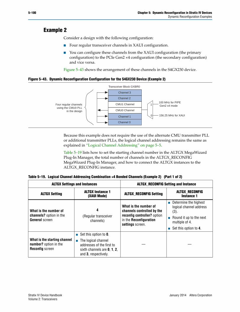
5–100 Chapter 5: Dynamic Reconfiguration in Stratix IV DevicesDynamic Reconfiguration Examples
Example 2Consider a design with the following configuration:
■ Four regular transceiver channels in XAUI configuration.
■ You can configure these channels from the XAUI configuration (the primary configuration) to the PCIe Gen2 ×4 configuration (the secondary configuration) and vice versa.
Figure 5–43 shows the arrangement of these channels in the S4GX230 device.
Because this example does not require the use of the alternate CMU transmitter PLL or additional transmitter PLLs, the logical channel addressing remains the same as explained in “Logical Channel Addressing” on page 5–5.
Table 5–19 lists how to set the starting channel number in the ALTGX MegaWizard Plug-In Manager, the total number of channels in the ALTGX_RECONFIG MegaWizard Plug-In Manager, and how to connect the ALTGX instances to the ALTGX_RECONFIG instance.
Figure 5–43. Dynamic Reconfiguration Configuration for the S4GX230 Device (Example 2)
Transceiver Block GXBR0
Channel 3
Channel 2
CMU1 Channel
CMU0 Channel
Channel 1
Channel 0
Four regular channelsusing the CMU0 PLL
in the design
1
0 156.25 MHz for XAUI
100 MHz for PIPE Gen2 x4 mode
Table 5–19. Logical Channel Addressing Combination ×4 Bonded Channels (Example 2) (Part 1 of 2)
ALTGX Settings and Instances ALTGX_RECONFIG Setting and Instance
ALTGX Setting ALTGX Instance 1(XAUI Mode) ALTGX_RECONFIG Setting ALTGX_RECONFIG
Instance 1
What is the number of channels? option in the General screen
4
(Regular transceiver channels)
What is the number of channels controlled by the reconfig controller? option in the Reconfiguration settings screen.
■ Determine the highest logical channel address (3).
■ Round it up to the next multiple of 4.
■ Set this option to 4.
What is the starting channel number? option in the Reconfig screen
■ Set this option to 0.
■ The logical channel addresses of the first to sixth channels are 0, 1, 2, and 3, respectively.
— —
Stratix IV Device Handbook January 2014 Altera CorporationVolume 2: Transceivers
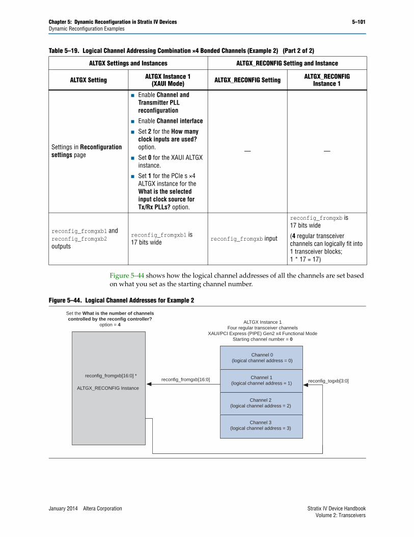
Chapter 5: Dynamic Reconfiguration in Stratix IV Devices 5–101Dynamic Reconfiguration Examples
Figure 5–44 shows how the logical channel addresses of all the channels are set based on what you set as the starting channel number.
Settings in Reconfiguration settings page
■ Enable Channel and Transmitter PLL reconfiguration
■ Enable Channel interface
■ Set 2 for the How many clock inputs are used? option.
■ Set 0 for the XAUI ALTGX instance.
■ Set 1 for the PCIe s ×4 ALTGX instance for the What is the selected input clock source for Tx/Rx PLLs? option.
— —
reconfig_fromgxb1 and reconfig_fromgxb2 outputs
reconfig_fromgxb1 is 17 bits wide reconfig_fromgxb input
reconfig_fromgxb is 17 bits wide
(4 regular transceiver channels can logically fit into 1 transceiver blocks;1 * 17 = 17)
Table 5–19. Logical Channel Addressing Combination ×4 Bonded Channels (Example 2) (Part 2 of 2)
ALTGX Settings and Instances ALTGX_RECONFIG Setting and Instance
ALTGX Setting ALTGX Instance 1(XAUI Mode) ALTGX_RECONFIG Setting ALTGX_RECONFIG
Instance 1
Figure 5–44. Logical Channel Addresses for Example 2
Set the What is the number of channelscontrolled by the reconfig controller?
option = 4
reconfig_fromgxb[16:0] *
ALTGX_RECONFIG Instance
reconfig_fromgxb[16:0]
ALTGX Instance 1Four regular transceiver channels
XAUI/PCI Express (PIPE) Gen2 x4 Functional ModeStarting channel number = 0
reconfig_togxb[3:0]
Channel 0(logical channel address = 0)
Channel 1(logical channel address = 1)
Channel 2(logical channel address = 2)
Channel 3(logical channel address = 3)
January 2014 Altera Corporation Stratix IV Device HandbookVolume 2: Transceivers
5–102 Chapter 5: Dynamic Reconfiguration in Stratix IV DevicesDynamic Reconfiguration Examples
Different Dynamic Reconfiguration Modes Involved
1. Channel and CMU PLL reconfiguration mode—used for reconfiguring four regular transceiver channels and the CMU0 PLL (in GXBR0) from XAUI mode to PCIe ×4 mode and vice versa.
1 Use this mode instead of channel reconfiguration with transmitter PLL select mode because the central clock divider used for bonded modes is only available in CMU0; therefore, you cannot use the CMU1 PLL as an alternate TX PLL.
2. Central control unit reconfiguration mode—used for reconfiguring central control unit logic used in bonded modes from XAUI mode to PCIe ×4 mode.
For more information, refer to “Transceiver Channel Reconfiguration Mode Details” on page 5–19.
.mif Generation
The following .mifs are required for this example:
■ One .mif is required to move from XAUI mode to PCIe ×4 mode
■ Another .mif is required to revert back to XAUI mode from PCIe ×4 mode
For more information, refer to “Memory Initialization File (.mif)” on page 5–20.
Various Dynamic Reconfiguration Transactions
The following dynamic reconfiguration transactions are required for this example:
■ .mif write transaction—for more information, refer to “Channel and CMU PLL Reconfiguration Mode Details” on page 5–24.
■ Alternatively, you may use reduced .mif reconfiguration. Reduced .mifs are generated using the altgx_diffmifgen.exe command. For more information, refer to “Reduced .mif Reconfiguration” on page 5–24.
Document Revision HistoryTable 5–20 lists the revision history for this chapter.
Table 5–20. Document Revision History (Part 1 of 2)
Date Version Changes
January 2014 3.6 ■ Updated the “Logical Channel Addressing of PMA-Only Channels” section.
November 2013 3.5 ■ Updated the “CMU PLL Reconfiguration Mode Details” section.
September 2012 3.4
■ Updated Table 5–13 title.
■ Updated Figure 5–6.
■ Updated Figure 5–37.
December 2011 3.3■ Updated the “Logical Channel Addressing of PMA-Only Channels” and “Transceiver
Channel Reconfiguration Mode Details” sections.
■ Updated Table 5–6, Table 5–9, and Table 5–16.
Stratix IV Device Handbook January 2014 Altera CorporationVolume 2: Transceivers
Chapter 5: Dynamic Reconfiguration in Stratix IV Devices 5–103Dynamic Reconfiguration Examples
February 2011 3.2
■ Updated Table 5–5, Table 5–6, and Table 5–16.
■ Updated Figure 5–1.
■ Updated the “Transceiver Channel Reconfiguration Mode Details”. “PMA Controls Reconfiguration Mode Details”, “Connecting the ALTGX and ALTGX_RECONFIG Instances”, “One Time Mode for a Single Channel”, “Applying a .mif in the User Design”, and “Functional Simulation of the Dynamic Reconfiguration Process” sections.
■ Removed the “Continuous Mode for a Single Channel” and “Powerdown for a Single Channel” sections.
■ Updated chapter title.
■ Applied new template.
■ Minor text edits.
March 2010 3.1
■ Updated Table 5–5, Table 5–6, Table 5–15, Table 5–16, and Table 5–17.
■ Updated Figure 5–1, Figure 5–14, Figure 5–16, Figure 5–26, and Figure 5–37.
■ Updated the “Blocks Reconfigured in the Data Rate Division in Transmitter Mode”, “Logical Channel Addressing of PMA-Only Channels”, “Central Control Unit Reconfiguration Mode Details”, “EyeQ”, “Error Indication During Dynamic Reconfiguration”, and “Functional Simulation of the Dynamic Reconfiguration Process” sections.
■ Added a note to the “Central Control Unit Reconfiguration Mode Details” section.
■ Minor text edits.
November 2009 3.0■ Completely re-wrote and re-organized chapter.
■ Updated all graphics and tables.
June 2009 2.1
■ Updated Figure 5–4, Figure 5–8, Figure 5–9, Figure 5–10, Figure 5–11, Figure 5–15, Figure 5–22, Table 5–37, Table 5–38, Figure 5–44, Figure 5–47, Figure 5–48, Figure 5–49, Figure 5–50, Figure 5–51, Figure 5–52, Figure 5–53, and Figure 5–54
■ Updated Table 5–2 and Table 5–31
■ Changed “logical_tx_pll_sel[1:0]” to “logical_tx_pll_sel” throughout
■ Updated “The reconfig_clk Clock Requirements for the ALTGX Instance and ALTGX_RECONFIG Instance”, “The logical_tx_pll_sel and logical_tx_pll_sel_en Ports”, “How to Use the logical_tx_pll_sel Port?”, and “When Can the logical_tx_pll_sel and logical_tx_pll_sel_en Ports be Used?”
■ Minor text edits
March 2009 2.0
Complete re-write and re-organization of the chapter.
Added or revised:
■ Offset Cancellation Control for Receiver Channels
■ PMA Controls Reconfiguration
■ Channel and CMU PLL Reconfiguration Mode
■ Data Rate Division in Transmitter: Operation
■ Channel Reconfiguration with Transmitter PLL Select Mode
■ CMU PLL Reconfiguration Mode
November 2008 1.0 Initial release.
Table 5–20. Document Revision History (Part 2 of 2)
Date Version Changes
January 2014 Altera Corporation Stratix IV Device HandbookVolume 2: Transceivers

5–104 Chapter 5: Dynamic Reconfiguration in Stratix IV DevicesDynamic Reconfiguration Examples
Stratix IV Device Handbook January 2014 Altera CorporationVolume 2: Transceivers


