

A New Floating Point ReadoutChip for CMS Calorimeters
R. Yarema, T. ZimmermanFermilab
September 2003
Sept. 29 – Oct. 3, 2003 9th Workshop on Electronics for LHC 2
Introduction
• The Floating Point Readout Chip for CMS HadronCalorimeters is the latest in a series of QIE chipsdesigned at Fermilab for processing signals. It iscalled QIE8.
• QIE stands for Charge (Q) Integrator and Encoder.• A QIE is a custom integrated circuit that accepts a
signal from a source such as a PMT or HPD anddigitizes the signal.
Sept. 29 – Oct. 3, 2003 9th Workshop on Electronics for LHC 3
CMS Hadron Calorimeter FrontEnd Readout Module
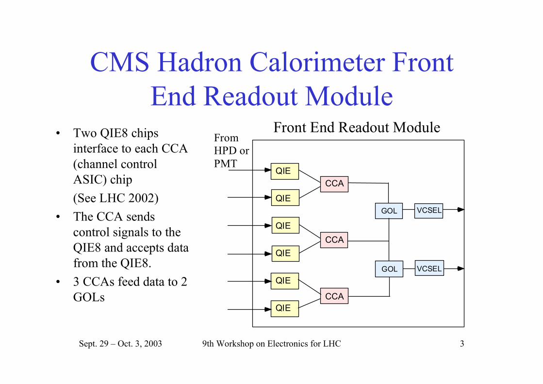
• Two QIE8 chipsinterface to each CCA(channel controlASIC) chip(See LHC 2002)
• The CCA sendscontrol signals to theQIE8 and accepts datafrom the QIE8.
• 3 CCAs feed data to 2GOLs
QIECCA
QIE
QIE
QIE
QIE
QIE
CCA
CCA
Front End Readout ModuleFromHPD orPMT
VCSEL
VCSEL
GOL
GOL VCSEL

Sept. 29 – Oct. 3, 2003 9th Workshop on Electronics for LHC 4
Hadron Calorimeter Front End Module
QIE CCA GOL

Sept. 29 – Oct. 3, 2003 9th Workshop on Electronics for LHC 5
QIE8 Chip Development• QIE8 designed in AMS 0.8 µm BiCMOS process.• First version of chip had a major problem in that operation
at 40 MHz was marginal at best.• Problem traced to poor model of P-channel devices.• AMS later acknowledged problem and provided new
models.• Second version of the chip was redesigned for different
PMOS models and included significant layout changesneeded to achieve desired performance.
• The second version was the production order!!
Sept. 29 – Oct. 3, 2003 9th Workshop on Electronics for LHC 6
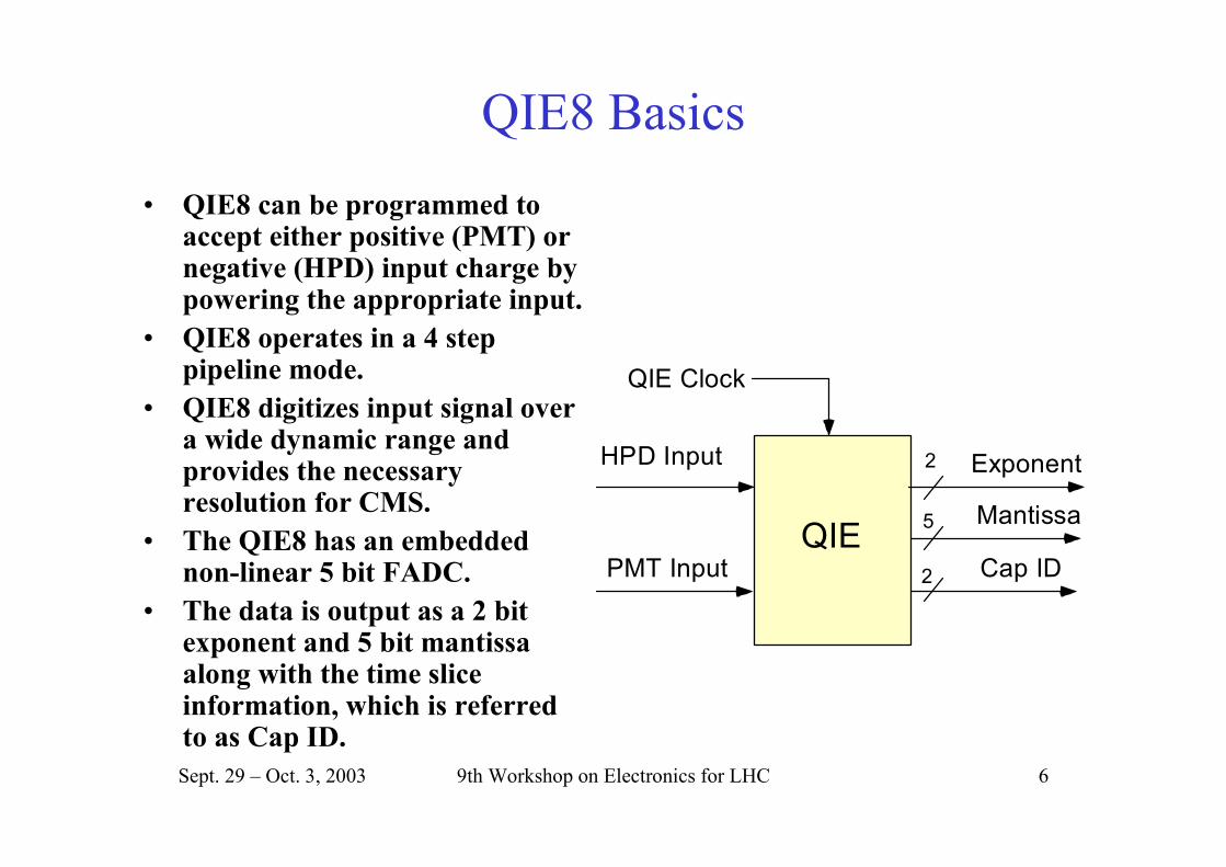
QIE8 Basics• QIE8 can be programmed to
accept either positive (PMT) ornegative (HPD) input charge bypowering the appropriate input.
• QIE8 operates in a 4 steppipeline mode.
• QIE8 digitizes input signal overa wide dynamic range andprovides the necessaryresolution for CMS.
• The QIE8 has an embeddednon-linear 5 bit FADC.
• The data is output as a 2 bitexponent and 5 bit mantissaalong with the time sliceinformation, which is referredto as Cap ID.
HPD Input
PMT InputQIE
Exponent
Mantissa
Cap ID
2
5
2
QIE Clock
Sept. 29 – Oct. 3, 2003 9th Workshop on Electronics for LHC 7
The QIE in a Nutshell
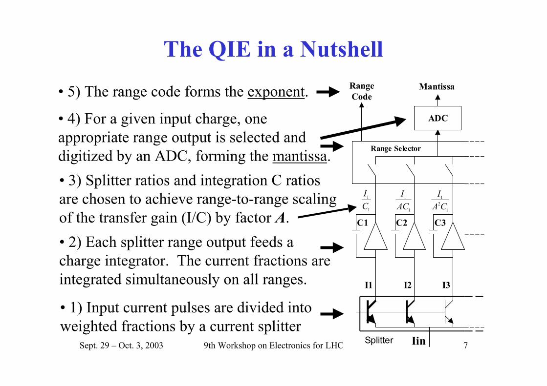
• 1) Input current pulses are divided intoweighted fractions by a current splitter
Iin
I1 I2 I3
Splitter
• 2) Each splitter range output feeds acharge integrator. The current fractions areintegrated simultaneously on all ranges.
C1 C2 C3
• 5) The range code forms the exponent. RangeCode
• 4) For a given input charge, oneappropriate range output is selected anddigitized by an ADC, forming the mantissa.
ADC
Mantissa
Range Selector
• 3) Splitter ratios and integration C ratiosare chosen to achieve range-to-range scalingof the transfer gain (I/C) by factor A.
1
1
CI
12
1
CAI
1
1
ACI

Sept. 29 – Oct. 3, 2003 9th Workshop on Electronics for LHC 8
QIE8 Specifications
• HPD (positive) input– QLSB = 1 fC (normal mode)– QLSB = 0.33 fC (cal. Mode)– Input impedance < 40 Ω– Input analog BW > 20 MHz– ENC (Cin = 30 pF) <0.5 fC
• PMT (negative) input– QLSB = 2.7 fC (norm mode)– QLSB = 0.9 fC (cal. mode)– Input impedance = 50/93 Ω– Input BW > 40 MHz– ENC (5m, 50 Ω cable), 2fC
Resolution = 2%QMAX/QLSB = 10,000 (>13 bits)Beam crossing time = 25 nsecADC DNL (small signals) <0.05 LSB

Sept. 29 – Oct. 3, 2003 9th Workshop on Electronics for LHC 9
Design Challenges• Custom FADC with very low DNL• Mixed mode analog/digital design• Must respond to positive and negative inputs.• Single power supply for easy operation• Controlled impedance inputs• High sensitivity inputs (1 fC/LSB for HPD)• Very high sensitivity calibration mode (1/3
fC/LSB to track detector response shiftsfrom radioactive source (200 e).
Sept. 29 – Oct. 3, 2003 9th Workshop on Electronics for LHC 10
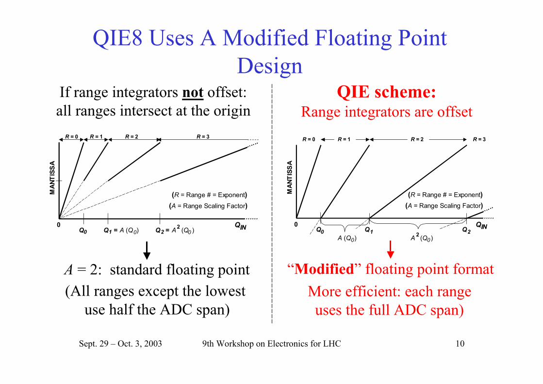
QIE8 Uses A Modified Floating PointDesign
MAN
TISS
A
QQ Q = A (Q )2A (Q )
R = 2R = 1R = 0
IN
(A = Range Scaling Factor)
R = 3
00 1
(R = Range # = Exponent)
0 0Q =2
If range integrators not offset:all ranges intersect at the origin
A = 2: standard floating point(All ranges except the lowest
use half the ADC span)M
ANTI
SSA
QQ Q Q
A (Q )2A (Q )
R = 2R = 1R = 0
IN
(A = Range Scaling Factor)
R = 3
00 1 2
(R = Range # = Exponent)
0 0
QIE scheme:Range integrators are offset
“Modified” floating point formatMore efficient: each rangeuses the full ADC span)
Sept. 29 – Oct. 3, 2003 9th Workshop on Electronics for LHC 11
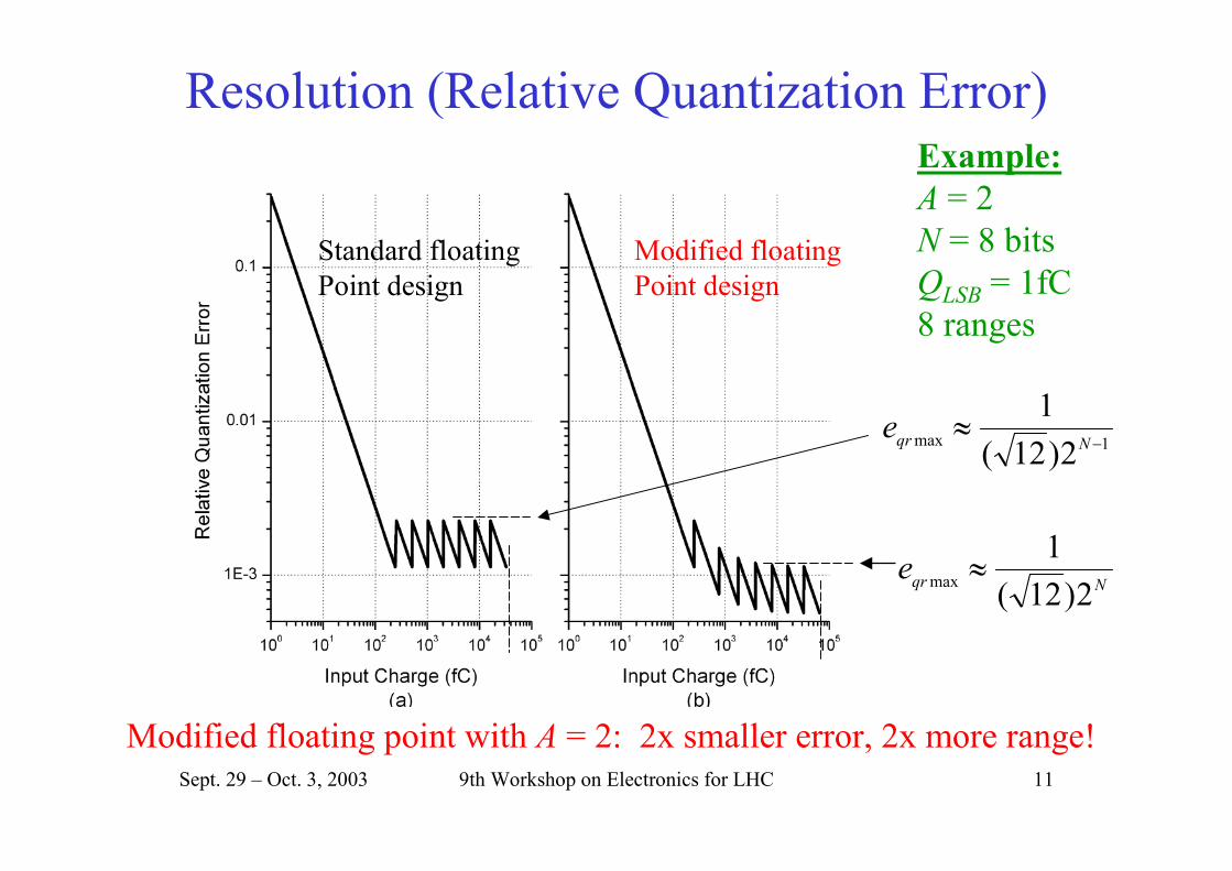
Resolution (Relative Quantization Error)
Modified floating point with A = 2: 2x smaller error, 2x more range!
Example:A = 2N = 8 bitsQLSB = 1fC8 ranges
1max 2)12(1
−≈
Nqre
Nqre 2)12(1
max ≈
Standard floatingPoint design
Modified floatingPoint design
Sept. 29 – Oct. 3, 2003 9th Workshop on Electronics for LHC 12
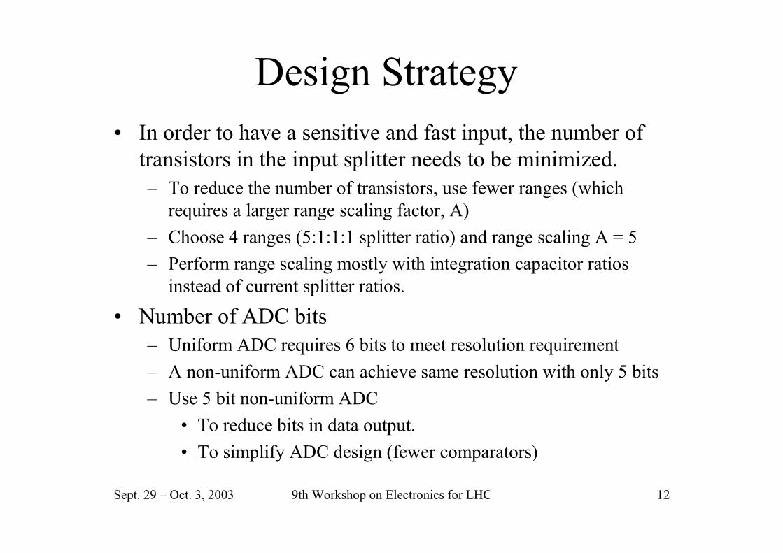
Design Strategy• In order to have a sensitive and fast input, the number of
transistors in the input splitter needs to be minimized.– To reduce the number of transistors, use fewer ranges (which
requires a larger range scaling factor, A)– Choose 4 ranges (5:1:1:1 splitter ratio) and range scaling A = 5– Perform range scaling mostly with integration capacitor ratios
instead of current splitter ratios.
• Number of ADC bits– Uniform ADC requires 6 bits to meet resolution requirement– A non-uniform ADC can achieve same resolution with only 5 bits– Use 5 bit non-uniform ADC
• To reduce bits in data output.• To simplify ADC design (fewer comparators)

Sept. 29 – Oct. 3, 2003 9th Workshop on Electronics for LHC 13
NON INVERTINGAMP/SPLITTER
(SIGNAL)
NON INVERTINGAMP/SPLITTER(REFERENCE)
INVERTINGAMP/SPLITTER
(SIGNAL)
INVERTINGAMP/SPLITTER(REFERENCE)
Phase 0Integrate andRange Select
EXP0SIG0REF0
EXP1 EXP2 EXP3SIG3SIG2SIG1
REF1 REF2 REF3
RSTCOMP0RSTCAP0INTEGRATE0
RSTCOMP1RSTCAP1INTEGRATE1
RSTCOMP2RSTCAP2INTEGRATE2
RSTCOMP3RSTCAP3INTEGRATE3
TIMING GENERATOR
INTE
GR
ATE
0-3
RST
CA
P0-3
RST
CO
MP0
-3
4 to 1DigitalMux
4 to 1Analog
Mux
4 to 1Analog
Mux
Pseudo-Differential
FlashADC
PHASE MUX
+
-
MANTISSA(4:0)
MU
X C
ON
TRO
L
FLA
SH C
LK
RES
ET
CLK
_IN
CAP_ID(1:0)
EXP0-3
SIG0-3
REF0-3
EXPONENT(1:0)
REFERENCEINPUT
SIGNALINPUT
NON INVERTINGMODE
INVERTINGMODE
Phase 1Integrate andRange Select
Phase 2Integrate andRange Select
Phase 3Integrate andRange Select
Isig
SIGNALINPUT
REFERENCEINPUT
Isig
Isig
/85I
sig/
8
Isig
/8Is
ig/8
Iref/8
5Ire
f/8
Iref/8
Iref/8
PMTinput
HPDinput
Pseudo-differential QIE configuration:Signal applied between SIG input and ground,REF input is “dummy.” QIE insensitive tobias, temp, supply V, common mode noise
Block Diagram

Sept. 29 – Oct. 3, 2003 9th Workshop on Electronics for LHC 14
Different Input Amps for PMT and HPD
Non-inverting InputAmplifier/Splitter
Inverting Input Amplifier/Splitter
I
+ X5 X1 X1 X1
5I/8 I/8 I/8 I/8
I
X3 X5 X1 X1 X1
5I/3 I/3 I/3 I/3
+
Negative input(PMT)
Non-inverting InputAmplifier/Splitter
Inverting Input Amplifier/Splitter
I
+ X5 X1 X1 X1
5I/8 I/8 I/8 I/8
I
X3 X5 X1 X1 X1
5I/3 I/3 I/3 I/3
+
Positive input(HPD)
Gain = -2.7
Signal Reference
Signal Reference
Note: a 4 range (5:1:1:1) splitter uses only 8 transistors
Sept. 29 – Oct. 3, 2003 9th Workshop on Electronics for LHC 15
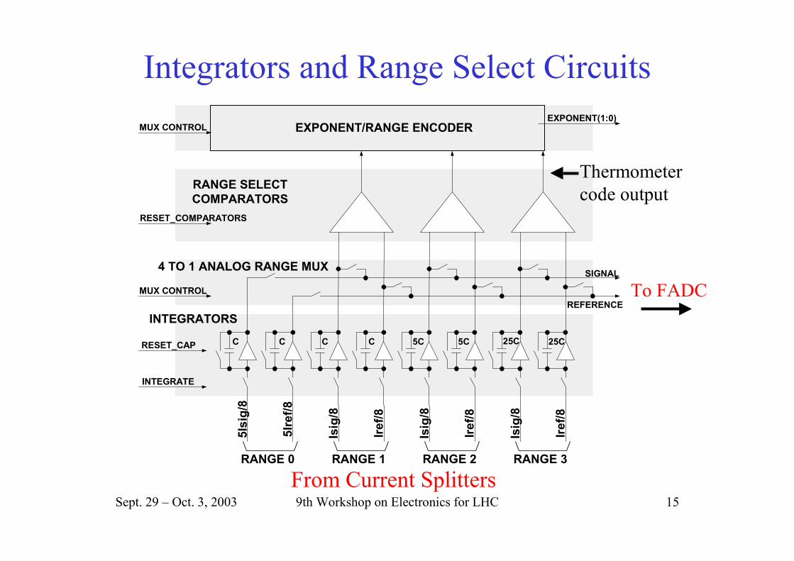
Integrators and Range Select CircuitsEXPONENT/RANGE ENCODER
C C C C 5C 5C 25C 25C
RANGE SELECTCOMPARATORS
INTEGRATORS
4 TO 1 ANALOG RANGE MUX
INTEGRATE
RESET_CAP
MUX CONTROL
MUX CONTROL
RESET_COMPARATORS
SIGNAL
REFERENCE
EXPONENT(1:0)
5Isi
g/8
5Ire
f/8
RANGE 0
Isig
/8
Iref/8
RANGE 1
Isig
/8
Iref/8
RANGE 2
Isig
/8
Iref/8
RANGE 3
To FADC
Thermometercode output
From Current Splitters
Sept. 29 – Oct. 3, 2003 9th Workshop on Electronics for LHC 16
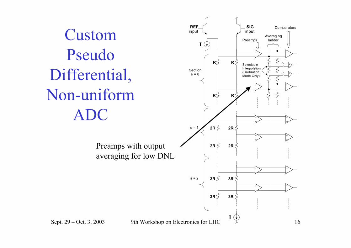
CustomPseudo
Differential,Non-uniform
ADC
SIGinput
R R
R R
Preamps
Comparators
Averagingladder
2R
2R
2R
2R
3R
3R
3R
3R
I
REFinput
+ +
+ +
+ +
+ +
+ +
+ +
I
SelectableInterpolation(CalibrationMode Only)
Sections = 0
s = 1
s = 2
Preamps with outputaveraging for low DNL
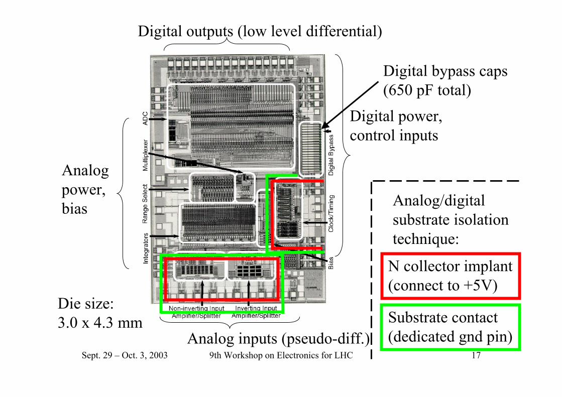
Sept. 29 – Oct. 3, 2003 9th Workshop on Electronics for LHC 17Analog inputs (pseudo-diff.)
Digital outputs (low level differential)
Digital bypass caps(650 pF total)
N collector implant(connect to +5V)
Substrate contact(dedicated gnd pin)
Analog/digitalsubstrate isolationtechnique:
Analogpower,bias
Digital power,control inputs
Die size:3.0 x 4.3 mm
Sept. 29 – Oct. 3, 2003 9th Workshop on Electronics for LHC 18
Production Testing• Received 25,079 packaged parts• Built robot chip tester (4 months) to handle parts
– Eliminates Post Doc burn out– Insures bad parts are sorted properly– Minimizes damage to pins due to handling– Tester holds 7 trays with 160 QIE8s per tray
• Tests all QIE8 functions– 18 major tests– Each test test may include hundreds of measurements
Sept. 29 – Oct. 3, 2003 9th Workshop on Electronics for LHC 19
QIE8 Chip Tester
Sept. 29 – Oct. 3, 2003 9th Workshop on Electronics for LHC 20
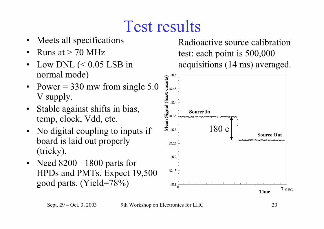
Test results• Meets all specifications• Runs at > 70 MHz• Low DNL (< 0.05 LSB in
normal mode)• Power = 330 mw from single 5.0
V supply.• Stable against shifts in bias,
temp, clock, Vdd, etc.• No digital coupling to inputs if
board is laid out properly(tricky).
• Need 8200 +1800 parts forHPDs and PMTs. Expect 19,500good parts. (Yield=78%)
Radioactive source calibrationtest: each point is 500,000acquisitions (14 ms) averaged.
180 e
7 sec
Sept. 29 – Oct. 3, 2003 9th Workshop on Electronics for LHC 21
Summary• Production quantity of QIE8 chips has been
received.• All chips have been packaged.• Testing with newly developed robot is
proceeding.• The robot has been so successful that a
second robot is being built.• QIE8 parts meet specifications.• Yield is good.


