

www.fairchildsemi.com 1
Dr. Janusz Bryzek, Dr. Shad Roundy Fairchild Semiconductor
Adoption of IC Packaging, Test and Reliability Advances for MEMS Devices

www.fairchildsemi.com 2
Brand Name Products with MEMS
Source: K. Yang, ADI presentation at COMS2008
Gyros & accels… A lot more than iDevices

www.fairchildsemi.com 3
Adding Sensor Degrees of Freedom Enables New Apps
3DOF Accelerometer
Orientation Sports User Interface
3DOF Gyroscope
Image Stabilization Smoother gaming Complex gestures
Altimeter
Location applications Indoor navigation Parking lots/Tall buildings Sports (Skiing, Gliding)
3DOF Magnetometer
Compassing Directional Heading Navigation
Temperature
Activity aware devices Medical Monitoring Sports Performance
+ + + +
3DOF
6DOF 9DOF
10DOF
11DOF
www.fairchildsemi.com 4
Outline
• Market drivers • Drivers for test and reliability standardization
• Packaging trends
• Reliability and testing
• Conclusions

www.fairchildsemi.com 5
Market Shift to Sense Based Intelligence

www.fairchildsemi.com 6
2011 Yole MEMS Forecast
Source: Yole Development
www.fairchildsemi.com 7
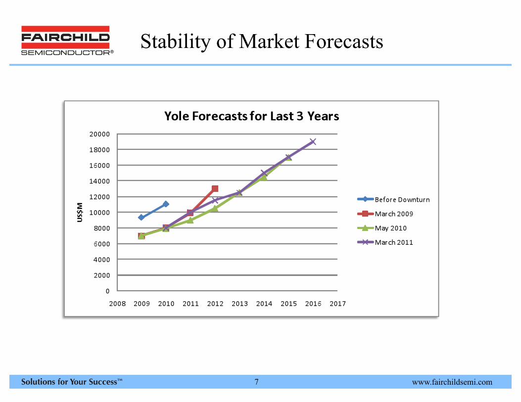
Stability of Market Forecasts

www.fairchildsemi.com 8
Emerged Mobile MEMS Applications
• Augmented reality • Point of Interest • Enhanced user interface • On line gaming • Location based services • 3D tagging • Indoor/outdoor navigation

www.fairchildsemi.com 9
MEMS for Personalized Healthcare
• Almost 7B people on earth. • Aging population. • Increasing lifespan.
• Increasing health cost. • $2.5 trillion in 2009 in the US alone.
• 18% of the GDP. • Remote home care emerges as Tornado in making to reduce health care cost.
• Initial focus: monitoring chronic conditions. • Wearable devices market (ABI Research):
• 2010: 12M devices (almost all of them for sports and fitness) • 2014: 420 million wearable health monitors
59 million used at home.

www.fairchildsemi.com 10
Trillion Sensors in this Decade?
10
Source: Hewlett Packard Development Co, Peter Hartwell, HP Labs

www.fairchildsemi.com 11
2011 MEMS – Current State
• Several applications exceeded $200M.
• MEMS law still in effect – “one product - one process – one package – one test procedure” • Cracks in the law are visible • LGA package dominates gyro and acceleration packaging from most vendors. • Test systems from selected vendors enable high speed testing of multiple sensor categories
(pressure, magnetic, acceleration, rate).
• Commercialization cycle is shrinking, but it is still: • At least 4 years. • 3-4 CEOs • $45M investment
• Potential for market to grow much larger (~$300B by some estimates), but several developments needed
• Faster learning cycles, 15 R&D cycles of learning per year • Develop 3D packaging • Develop platform processes • Form development and manufacturing super groups • Open-mindedness and curiosity

www.fairchildsemi.com 12
PACKAGING TRENDS
12
www.fairchildsemi.com 13
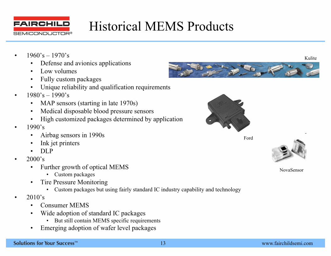
Historical MEMS Products
• 1960’s – 1970’s • Defense and avionics applications • Low volumes • Fully custom packages • Unique reliability and qualification requirements
• 1980’s – 1990’s • MAP sensors (starting in late 1970s) • Medical disposable blood pressure sensors • High customized packages determined by application
• 1990’s • Airbag sensors in 1990s • Ink jet printers • DLP
• 2000’s • Further growth of optical MEMS
• Custom packages • Tire Pressure Monitoring
• Custom packages but using fairly standard IC industry capability and technology • 2010’s
• Consumer MEMS • Wide adoption of standard IC packages
• But still contain MEMS specific requirements • Emerging adoption of wafer level packages
Kulite
Ford
NovaSensor
www.fairchildsemi.com 14
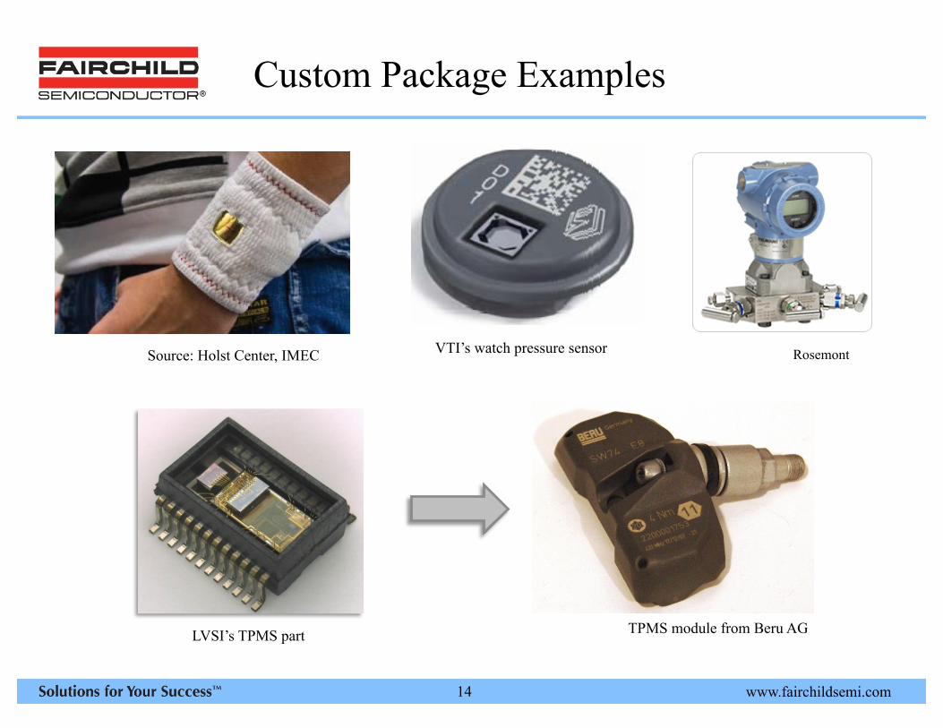
Custom Package Examples
VTI’s watch pressure sensor Source: Holst Center, IMEC Rosemont
TPMS module from Beru AG LVSI’s TPMS part

www.fairchildsemi.com 15
Amkor MEMS Packaging Matrix
Source: Amkor
www.fairchildsemi.com 16
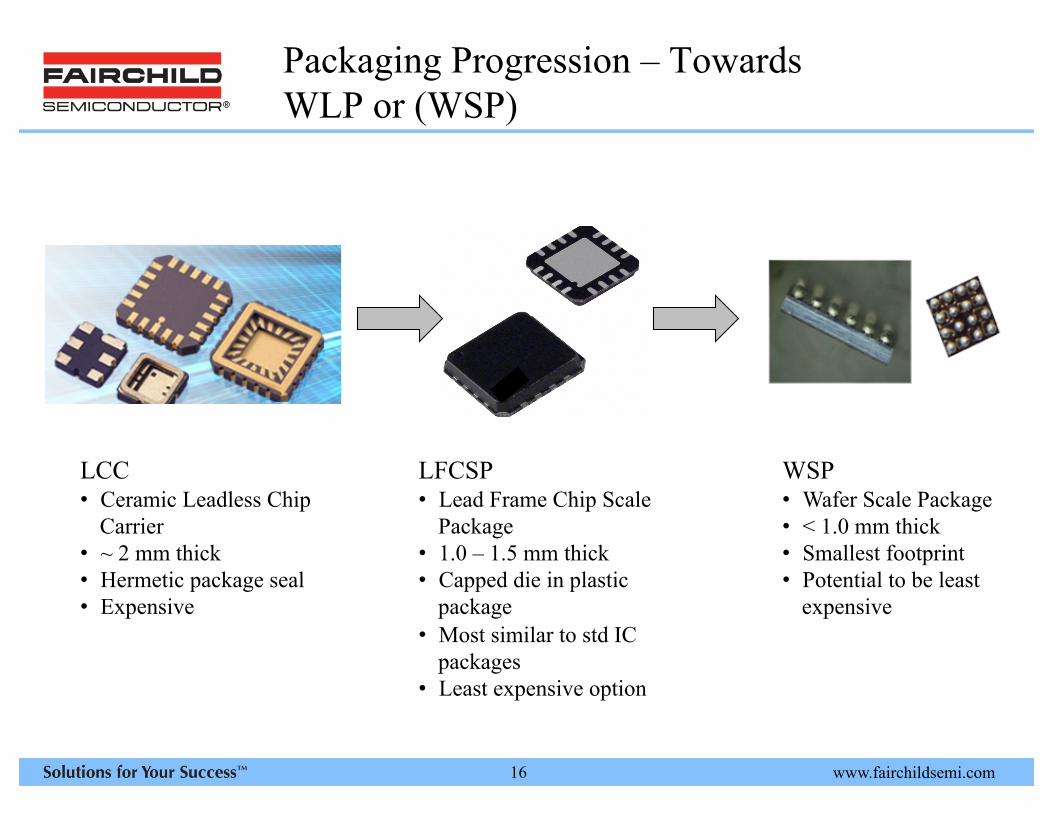
Packaging Progression – Towards WLP or (WSP)
LCC • Ceramic Leadless Chip
Carrier • ~ 2 mm thick • Hermetic package seal • Expensive
LFCSP • Lead Frame Chip Scale
Package • 1.0 – 1.5 mm thick • Capped die in plastic
package • Most similar to std IC
packages • Least expensive option
WSP • Wafer Scale Package • < 1.0 mm thick • Smallest footprint • Potential to be least
expensive

www.fairchildsemi.com 17
Enabling Technologies for Wafer Level MEMS Packaging
• Wafer Bonding • Eutectic Bonding • Silicon Fusion Bonding
• Zero kerf wafer dicing • Thin wafer handling
• More difficult for MEMS because of internal cavities and stresses • Need to handle different thicknesses
• Through Silicon VIAs (TSV) • Vertical TSVs for MEMS • Vertical TSVs through ASIC • Silicon interposers
• Blank silicon with VIA • Lateral VIAs
www.fairchildsemi.com 18
Packaging Requirements
• Small percentage of devices will use non-IC type packaging • E.g., process control transmitters
• Majority will have to use IC-derived packaging as it offers the best cost • Major categories of MEMS packaging:
• Optical, enabling light transmission • Display, spectrometers
• Open to the silicon chip for air/fluid access • Pressure sensors, microphones, Lab-on-Chip, gas chromatographs chemical
sensors, ink-jet nozzles, • IC-like with some stress control
• Acceleration sensors, gyros, RF switches and filters, resonators • Specialty
• Scavengers, etc.
www.fairchildsemi.com 19
State of MEMS Packaging 2011
• Drive toward Standard IC Packages • Currently most MEMS use some form of modified IC package • Inertial sensors especially look more and more like standard IC
packages • Move to all silicon (wafer level package)
• Reliability issues associated with MEMS • Shock for example
• Testing issues • Fixtures and infrastructure • Some packaging solutions do not allow MEMS to be tested without ASIC
• Puts higher priority on design for test

www.fairchildsemi.com 20
RELIABILITY AND TEST
20

www.fairchildsemi.com 21
Reliability Standards for MEMS
• Standard IC reliability tests used • AEC-Q100 also widely used • Many device specific reliability issues for which there aren’t good
standards • Stiction is an excellent example
• Universal MEMS standards do not exist • Standards could help reduce test cost and time to market • Diversity of products makes this more difficult • Where to start?
• Device level • Inertial sensors

www.fairchildsemi.com 22
MEMS Reliability Tests
• Microelectronics and ICs • Accelerated life tests
• Thermal cycle, thermal shock, HAST, etc. • The goal of accelerated life tests is to determine the probability of “wear out”
• Burn in tests (temperature and humidity) • The goal of burn in tests is to have “infant mortality” occur in the factory, not in the field
• MEMS devices • All of the above! • Failure by mechanical causes - shock, vibration • Shipping / handling and in service performance • Media contact
• Pressure diaphragm for example
Useful Life
Wear Out
Infant Mortality
Adapted from “Overview of the Current State of MEMS Reliability and Test” Mehran Mehregany, Case Western Reserve University

www.fairchildsemi.com 23
Failure Mechanisms in MEMS and Microsystems
Failure Mode Causes Probability
Mechanical Local stress concentration due to surface roughness Low
Improper assembly tolerances Moderate
Vibration-induced high cycle fatigue failure. Low in silicon Moderate in plastic
Delamination of thin layers. Moderate to high
Thermal stresses by mismatch of CTE High
Electromechanical break-down
Collapse of electrodes due to excessive deformation High
Deterioration of materials Aging and degassing of plastic and polymers. Corrosion and erosion of materials.
Moderate
Excessive intrinsic stresses Residual stresses and molecular forces inherent from microfabrication
High
Packaging Improper bonding and sealing, poor die protection and isolation
High
Environmental effects Temperature, humidity, dusts and toxic gas High
“Overview of the Current State of MEMS Reliability and Test” Mehran Mehregany, Case Western Reserve University

www.fairchildsemi.com 24
MIG Testing Standards Workshop
• When we began our journey in the summer of 2010, we asked you to "imagine a world" with MEMS standards. Working with our members and partners, MEMS Industry Group (MIG) worked to identify and document device level qualification and testing needs. We also set out to document the results as a guide to where to focus R&D and standards development for device testing on inertial devices. The ultimate goal is to help reduce MEMS manufacturing costs by up to 60%; a number often attributed to the cost of MEMS testing.
• In collaboration with our members and partners, MIG is pleased to announce the first step in this journey - the release of MEMS Testing Standards: A Path to Continued Innovation - Report on MEMS Testing Standards Workshop. We encourage you to view/download the document, join the discussion, and contact MIG to be a part of the next steps that are outlined in the report.

www.fairchildsemi.com 25
Solidus Dynamic Wafer Level Testing
Tests the “Dynamic” Mechanical Performance of MEMS Capacitive Elements at Wafer-Level, including Natural Frequency, Damping, Quality Factor, Stiction, Gyro Quadrature Error, Frequency, Phase, Amplitude and others.
STI3000 Wafer Probe Test System Solidus Technologies Leveraging Engineering for the Future
www.fairchildsemi.com 26
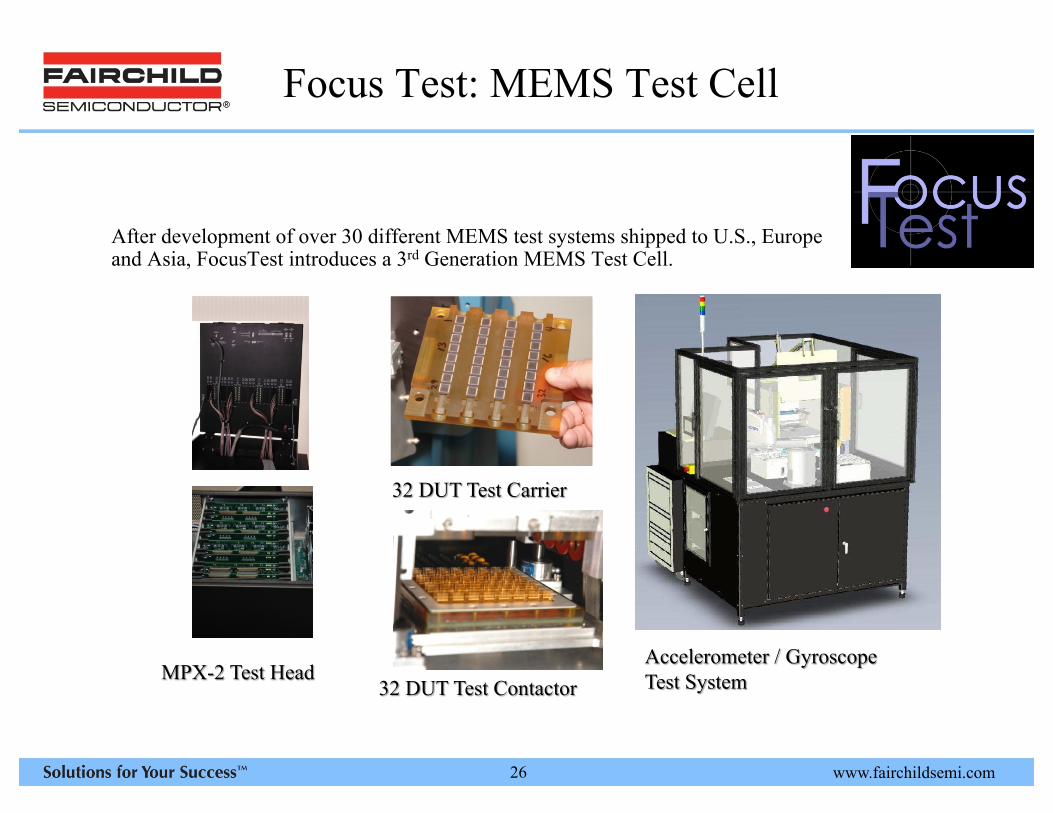
Focus Test: MEMS Test Cell
After development of over 30 different MEMS test systems shipped to U.S., Europe and Asia, FocusTest introduces a 3rd Generation MEMS Test Cell.

www.fairchildsemi.com 27
Multi-Test System
Source: Semicon Taiwan 2010

www.fairchildsemi.com 28
Centipede Test Systems
Source: T. H. Di Stefano
32 DUT Flex Frame Carrier
Automated Test-in-Tray System
Pressure Sensor Test Head
www.fairchildsemi.com 29
Test Summary
• Standards are lacking, but progress is being made • Diversity of MEMS will always require a certain amount
of custom test procedures and test systems • Test systems infrastructure is now quite well developed
for inertial, pressure, and magnetic sensors

www.fairchildsemi.com 30
Conclusions
• MEMS continues to have very strong growth • Current consumer MEMS Tornado • Potential future Tornados in area of personal health monitoring and wearable devices
• Current consumer MEMS focus is pushing packaging towards more standardization with IC packages
• High volumes in inertial, pressure, and magnetic are driving a more mature production test infrastructure
• Both of these developments are reducing development time and costs • MEMS does, and will continue to have, unique reliability and test requirements • New high volume MEMS developments rely almost exclusively on large
packaging vendors, no start-up companies are visible yet • Big companies need to expand coverage of MEMS applications

www.fairchildsemi.com 31
Thank You


