
AN 778: Intel® Stratix® 10Transceiver Usage
SubscribeSend Feedback
AN-778 | 2019.03.07Latest document on the web: PDF | HTML
Contents
1. Transceiver Layout......................................................................................................... 31.1. L-Tile and H-Tile Overview.......................................................................................4
1.1.1. PLLs.........................................................................................................41.1.2. Transmitter Clock Network ......................................................................... 81.1.3. GXT Clock Network.................................................................................. 121.1.4. Calibration.............................................................................................. 15
2. Tile Architecture Constraints.........................................................................................162.1. Transceiver Channel Placement .............................................................................16
2.1.1. Possible Combinations of GX and GXT Channels........................................... 162.1.2. GX Channels........................................................................................... 212.1.3. GXT Channels..........................................................................................232.1.4. Reference Clock Guidelines for L-Tile and H-Tile............................................292.1.5. PLL Placement......................................................................................... 30
2.2. Unsupported Dynamic Reconfiguration Features....................................................... 352.3. Intel Stratix 10 L-Tile Transceiver to H-Tile Transceiver Migration................................ 352.4. Thermal Guidelines.............................................................................................. 36
3. PCIe Guidelines.............................................................................................................373.1. PCIe Hard IP....................................................................................................... 37
3.1.1. Channel Placement for PCIe Hard IP........................................................... 373.1.2. PLL Placement for PCIe Hard IP..................................................................38
3.2. PHY Interface for PCIe Express (PIPE).....................................................................413.2.1. Channel Placement for PIPE.......................................................................413.2.2. PLL Placement for PIPE............................................................................. 41
4. Document Revision History for AN 778: Intel Stratix 10 Transceiver Usage..................42
Contents
AN 778: Intel® Stratix® 10 Transceiver Usage Send Feedback
2
1. Transceiver LayoutNote: This app note currently covers Intel® Stratix® 10 L-Tile ES1, L-Tile and H-Tile (L-
Tile/H-Tile) information. E-Tile information will be available in a future document.
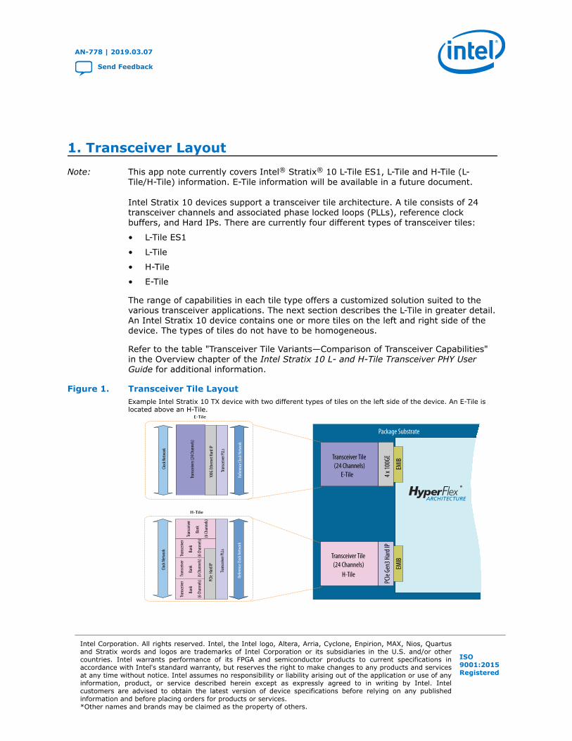
Intel Stratix 10 devices support a transceiver tile architecture. A tile consists of 24transceiver channels and associated phase locked loops (PLLs), reference clockbuffers, and Hard IPs. There are currently four different types of transceiver tiles:
• L-Tile ES1
• L-Tile
• H-Tile
• E-Tile
The range of capabilities in each tile type offers a customized solution suited to thevarious transceiver applications. The next section describes the L-Tile in greater detail.An Intel Stratix 10 device contains one or more tiles on the left and right side of thedevice. The types of tiles do not have to be homogeneous.
Refer to the table "Transceiver Tile Variants—Comparison of Transceiver Capabilities"in the Overview chapter of the Intel Stratix 10 L- and H-Tile Transceiver PHY UserGuide for additional information.
Figure 1. Transceiver Tile LayoutExample Intel Stratix 10 TX device with two different types of tiles on the left side of the device. An E-Tile islocated above an H-Tile.
Transceiver Tile (24 Channels) E-Tile
H-Tile
Package Substrate
4
x 10
0GE
EMIB
Trans
ceive
r
Bank
(6 Ch
anne
ls)
Trans
ceive
r PLL
s
Trans
ceive
r
Bank
(6 Ch
anne
ls)
Trans
ceive
r
Bank
(6 Ch
anne
ls)PC
Ie H
ard I
P
Refer
ence
Cloc
k Net
work
Clock
Net
work
Trans
ceive
r
Bank
(6 Ch
anne
ls)
Transceiver Tile (24 Channels)
H-Tile
PCIe
Gen3
Har
d IP
EMIB
®
Trans
ceive
r PLL
s
100G
Ethe
rnet
Har
d IP
Refer
ence
Cloc
k Net
work
Clock
Net
work
Trans
ceive
rs (2
4 Cha
nnels
)
E-Tile
AN-778 | 2019.03.07
Send Feedback
Intel Corporation. All rights reserved. Intel, the Intel logo, Altera, Arria, Cyclone, Enpirion, MAX, Nios, Quartusand Stratix words and logos are trademarks of Intel Corporation or its subsidiaries in the U.S. and/or othercountries. Intel warrants performance of its FPGA and semiconductor products to current specifications inaccordance with Intel's standard warranty, but reserves the right to make changes to any products and servicesat any time without notice. Intel assumes no responsibility or liability arising out of the application or use of anyinformation, product, or service described herein except as expressly agreed to in writing by Intel. Intelcustomers are advised to obtain the latest version of device specifications before relying on any publishedinformation and before placing orders for products or services.*Other names and brands may be claimed as the property of others.
ISO9001:2015Registered
Related Information
Overview
1.1. L-Tile and H-Tile Overview
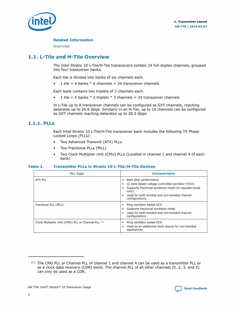
The Intel Stratix 10 L-Tile/H-Tile transceivers contain 24 full-duplex channels, groupedinto four transceiver banks.
Each tile is divided into banks of six channels each.
• 1 tile = 4 banks * 6 channels = 24 transceiver channels
Each bank contains two triplets of 3 channels each.
• 1 tile = 4 banks * 2 triplets * 3 channels = 24 transceiver channels
In L-Tile up to 8 transceiver channels can be configured as GXT channels, reachingdatarates up to 26.6 Gbps. Similarly in an H-Tile, up to 16 channels can be configuredas GXT channels reaching datarates up to 28.3 Gbps.
1.1.1. PLLs
Each Intel Stratix 10 L-Tile/H-Tile transceiver bank includes the following TX PhaseLocked Loops (PLLs):
• Two Advanced Transmit (ATX) PLLs
• Two Fractional PLLs (fPLL)
• Two Clock Multiplier Unit (CMU) PLLs (Located in channel 1 and channel 4 of eachbank)
Table 1. Transmitter PLLs in Stratix 10 L-Tile/H-Tile Devices
PLL Type Characteristics
ATX PLL • Best jitter performance• LC tank based voltage controlled oscillator (VCO)• Supports fractional synthesis mode (in cascade mode
only)• Used for both bonded and non-bonded channel
configurations
Fractional PLL (fPLL) • Ring oscillator based VCO• Supports fractional synthesis mode• Used for both bonded and non-bonded channel
configurations
Clock Multiplier Unit (CMU) PLL or Channel PLL (1) • Ring oscillator based VCO• Used as an additional clock source for non-bonded
applications
(1) The CMU PLL or Channel PLL of channel 1 and channel 4 can be used as a transmitter PLL oras a clock data recovery (CDR) block. The channel PLL of all other channels (0, 2, 3, and 5)can only be used as a CDR.
1. Transceiver Layout
AN-778 | 2019.03.07
AN 778: Intel® Stratix® 10 Transceiver Usage Send Feedback
4
The total number of TX PLLs per tile is:
• Eight ATX PLLs (2 ATX PLLs per bank * 4 banks per tile)
• Eight fPLLs (2 fPLLs per bank * 4 banks per tile)
• Eight CMU PLLs (2 CMU PLLs per bank * 4 banks per tile)
1. Transceiver Layout
AN-778 | 2019.03.07
Send Feedback AN 778: Intel® Stratix® 10 Transceiver Usage
5

Figure 2. Stratix 10 PLLs and Clock Networks in Two Banks of Intel Stratix 10 L-Tile/H-TileThe ATX PLL, fPLL and CMU PLLs can drive the x1 clock network to support non-bonded transceivers. The ATXPLL and fPLL can drive the x6 clock network to support bonded transceivers within the bank. The x6 clocknetwork can drive the x24 clock network in adjacent banks, allowing ATX PLLs and fPLLs to support up to 24bonded transceiver channels. The x1, x6, and x24 clock networks are described in the Transceiver ClockNetwork section.
Local CGB
CDRCH2
Local CGB
CDR/CMUCH1
Local CGB
CDRCH0
fPLL
ATXPLL
MasterCGB
Local CGB
CDRCH5
Local CGB
CDR/CMUCH4
Local CGB
CDRCH3
fPLL
ATXPLL
MasterCGB
Local CGB
CDRCH2
Local CGB
CDR/CMUCH1
Local CGB
CDRCH0
fPLL
ATXPLL
MasterCGB
Local CGB
CDRCH5
Local CGB
CDR/CMUCH4
Local CGB
CDRCH3
fPLL
ATXPLL
MasterCGB
x1 Clock Lines x6 Clock Lines x24 Clock LinesTransceiver
Bank
TransceiverBank
Note: For further details on CGB, refer to "PLL and Clock Networks" chapter in Intel Stratix10 L- and H-Tile Transceiver PHY User Guide.
1. Transceiver Layout
AN-778 | 2019.03.07
AN 778: Intel® Stratix® 10 Transceiver Usage Send Feedback
6
Related Information
• Transmitter Clock Network on page 8
• PLL and Clock Networks
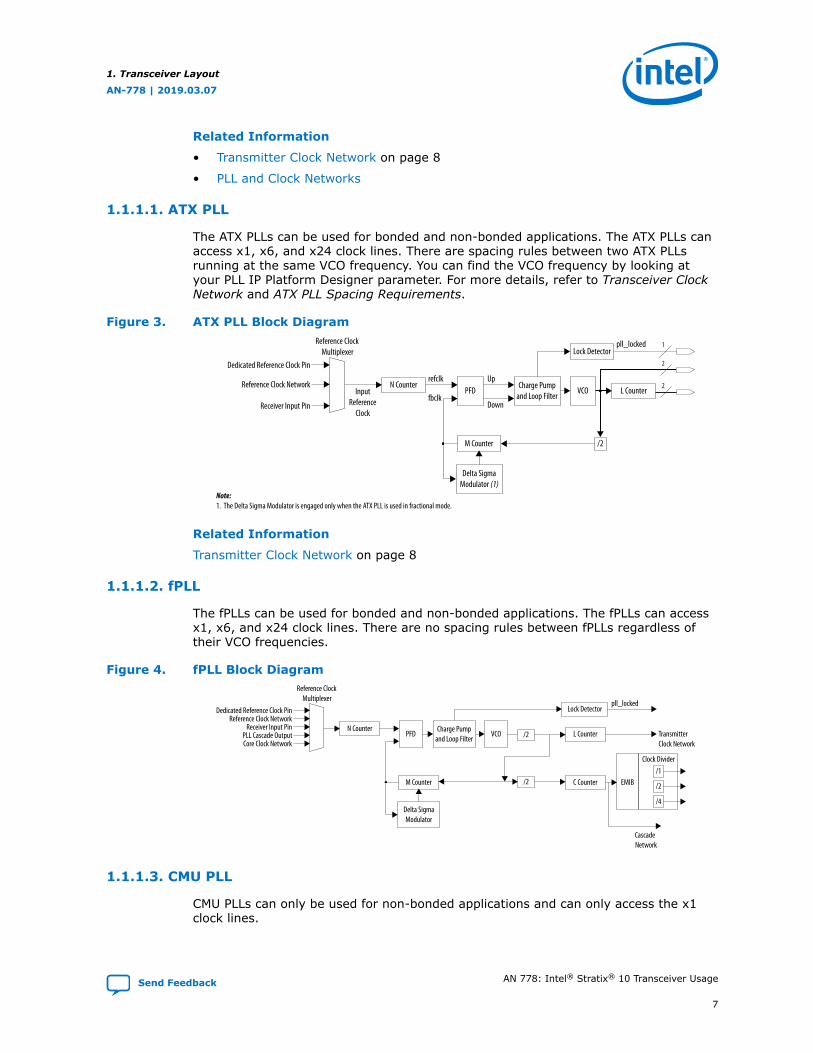
1.1.1.1. ATX PLL
The ATX PLLs can be used for bonded and non-bonded applications. The ATX PLLs canaccess x1, x6, and x24 clock lines. There are spacing rules between two ATX PLLsrunning at the same VCO frequency. You can find the VCO frequency by looking atyour PLL IP Platform Designer parameter. For more details, refer to Transceiver ClockNetwork and ATX PLL Spacing Requirements.
Figure 3. ATX PLL Block Diagram
Note:1. The Delta Sigma Modulator is engaged only when the ATX PLL is used in fractional mode.
N Counter
M Counter
L CounterPFDCharge Pump
and Loop FilterVCO
Delta SigmaModulator (1)
Dedicated Reference Clock Pin
Reference Clock Network
Receiver Input Pin
Reference ClockMultiplexer
/2
InputReference
Clock
refclk Up
Down
Lock Detector
2
2
pll_locked
fbclk
1
Related Information
Transmitter Clock Network on page 8
1.1.1.2. fPLL
The fPLLs can be used for bonded and non-bonded applications. The fPLLs can accessx1, x6, and x24 clock lines. There are no spacing rules between fPLLs regardless oftheir VCO frequencies.
Figure 4. fPLL Block Diagram
N Counter
M Counter
L Counter
C Counter
PFDCharge Pump
and Loop FilterVCO
Delta SigmaModulator
Dedicated Reference Clock Pin
TransmitterClock Network
Reference Clock NetworkReceiver Input Pin
PLL Cascade OutputCore Clock Network
Reference ClockMultiplexer
EMIB/1
/2
/4
Clock Divider
Lock Detectorpll_locked
/2
/2
CascadeNetwork
1.1.1.3. CMU PLL
CMU PLLs can only be used for non-bonded applications and can only access the x1clock lines.
1. Transceiver Layout
AN-778 | 2019.03.07
Send Feedback AN 778: Intel® Stratix® 10 Transceiver Usage
7

When using a CMU PLL in channel 1 or channel 4 of a bank, that channel is no longeravailable to receive data, but the channel can still be used for transmitting data.
Figure 5. CMU PLL Block Diagram
OutputN Counter
M Counter
L CounterPFDCharge Pump
and Loop FilterVCO
Reference Clock NetworkReceiver Input Pin
Reference ClockMultiplexer
InputReference
Clock
refclk Up
Down
Lock Detector
fbclk
PLL Lock Status
Lock toReferenceController
User Control(LTR/LTD) Lock to Reference
1.1.2. Transmitter Clock Network
The transmitter clock network routes the clock from the transmitter PLL to one ormore transmitter channels. It provides two types of clocks to the transmitter channel:
• High-Speed Serial Clock - high-speed clock for the serializer
• Low-Speed Parallel Clock - low-speed clock for the serializer and the PCS
In a bonded channel configuration, both the serial clock and the parallel clock arerouted from the transmitter PLL to the transmitter channels. In a non-bonded channelconfiguration, only the serial clock is routed to the transmitter channels, while theparallel clock is generated locally within each channel.
To support various bonded and non-bonded clocking configurations, three types oftransmitter clock network lines are available:
• x1 clock lines: Span a single bank within a tile and are used for non-bondedchannel clocking only
• x6 clock lines: Span a single bank within a tile and are used for bonded channelclocking
• x24 clock lines: Span all banks within a tile and are used for both PMA bonded andPMA-PCS bonded transceiver channels.
All clock lines are contained within a single tile and cannot span across multiple tiles.
1. Transceiver Layout
AN-778 | 2019.03.07
AN 778: Intel® Stratix® 10 Transceiver Usage Send Feedback
8
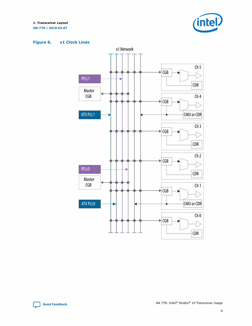
Figure 6. x1 Clock Lines
CMU or CDR
CGBCh 4
CDR
CGBCh 3
CDR
CGBCh 2
CGBCh 1
CDR
CGBCh 0
CDR
CGBCh 5
x1 Network
MasterCGB
MasterCGB
ATX PLL1
ATX PLL0
fPLL1
fPLL0
CMU or CDR
1. Transceiver Layout
AN-778 | 2019.03.07
Send Feedback AN 778: Intel® Stratix® 10 Transceiver Usage
9

Figure 7. x6 Clock Lines
CGBCh 4
CDR
CGBCh 3
CDR
CGBCh 2
CGBCh 1
CDR
CGBCh 0
CDR
CGBCh 5
MasterCGB
MasterCGB
x6Top
x6Bottom
x6Network
CMU or CDR
CMU or CDR
1. Transceiver Layout
AN-778 | 2019.03.07
AN 778: Intel® Stratix® 10 Transceiver Usage Send Feedback
10
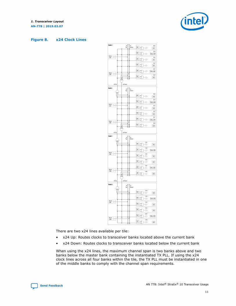
Figure 8. x24 Clock Lines
CGBCh 4
CDRCGB
Ch 3
CDRCGB
Ch 2
CGBCh 1
CDRCGB
Ch 0
CDRCGB
Ch 5
x6Top
MasterCGB1
MasterCGB0
x6Bottom
CMU or CDR
CMU or CDR
CGBCh 4
CDRCGB
Ch 3
CDRCGB
Ch 2
CGBCh 1
CDRCGB
Ch 0
CDRCGB
Ch 5
x6Top
MasterCGB1
MasterCGB0
x6Bottom
x24 Up x24 Down
CMU or CDR
CMU or CDR
CGBCh 4
CDRCGB
Ch 3
CDRCGB
Ch 2
CGBCh 1
CDRCGB
Ch 0
CDRCGB
Ch 5x6Top
MasterCGB1
MasterCGB0
x6Bottom
x24 Up x24 Down
CMU or CDR
CMU or CDR
CGBCh 4
CDRCGB
Ch 3
CDRCGB
Ch 2
CGBCh 1
CDRCGB
Ch 0
CDRCGB
Ch 5
x6Top
MasterCGB1
MasterCGB0
x6Bottom
x24 Up x24 Down
CMU or CDR
CMU or CDR
Bank 3
Bank 2
Bank 1
Bank 0
There are two x24 lines available per tile:
• x24 Up: Routes clocks to transceiver banks located above the current bank
• x24 Down: Routes clocks to transceiver banks located below the current bank
When using the x24 lines, the maximum channel span is two banks above and twobanks below the master bank containing the instantiated TX PLL. If using the x24clock lines across all four banks within the tile, the TX PLL must be instantiated in oneof the middle banks to comply with the channel span requirements.
1. Transceiver Layout
AN-778 | 2019.03.07
Send Feedback AN 778: Intel® Stratix® 10 Transceiver Usage
11

Related Information
• PLL and Clock Networks
• Channel Bonding
1.1.2.1. Bonded Transceiver Channels - Guidelines for VCCR_GXB and VCCT_GXB
Table 2. Voltage RequirementsFor transceiver channels that require bonding via the x6/x24 transceiver clock networks, refer to this table forspecific voltage requirements.
Channel Type Transceiver LinkType Data Rate VCCR_GXB/VCCT_GXB Typical
Min Typical Max
GX Chip to Chip andBackplane
1 Gbps to 16Gbps 1 V 1.03 V 1.06 V
16 Gbps to 17.4Gbps 1.1 V 1.12 V 1.14 V
GXT Chip to Chip andBackplane > 17.4 Gbps N/A (Bonding is not supported)
For non-bonded transceiver channels, refer to the "Transceiver Power SupplyOperating Conditions" in the Intel Stratix 10 Device Datasheet.
Related Information
Intel Stratix 10 Device Datasheet
1.1.3. GXT Clock Network
Both the L-Tile and H-Tile contains the GXT clock network. The GXT clock networkallows an ATX PLL to drive up to six transmitter channels—four in its bank and two inan adjacent bank. The GXT clock network is used for data rates above 17.4 Gbps. ForL-Tile and H-Tile GXT channel specification, please refer to "GXT Channels" section formore details.
Note: Intel Stratix 10 L-Tile ES1 does not support GXT clock network.
1. Transceiver Layout
AN-778 | 2019.03.07
AN 778: Intel® Stratix® 10 Transceiver Usage Send Feedback
12
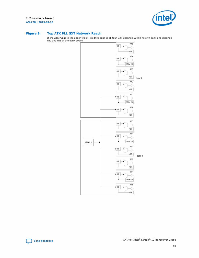
Figure 9. Top ATX PLL GXT Network ReachIf the ATX PLL is in the upper triplet, its drive span is all four GXT channels within its own bank and channelsch0 and ch1 of the bank above.
CMU or CDR
CGBCh 4
CDR
CGBCh 3
CDR
CGBCh 2
CGBCh 1
CDR
CGBCh 0
CDR
CGBCh 5
CMU or CDR
CMU or CDR
CGBCh 4
CDR
CGBCh 3
CDR
CGBCh 2
CGBCh 1
CDR
CGBCh 0
CDR
CGBCh 5
CMU or CDR
ATX PLL 1
Bank 1
Bank 0
1. Transceiver Layout
AN-778 | 2019.03.07
Send Feedback AN 778: Intel® Stratix® 10 Transceiver Usage
13
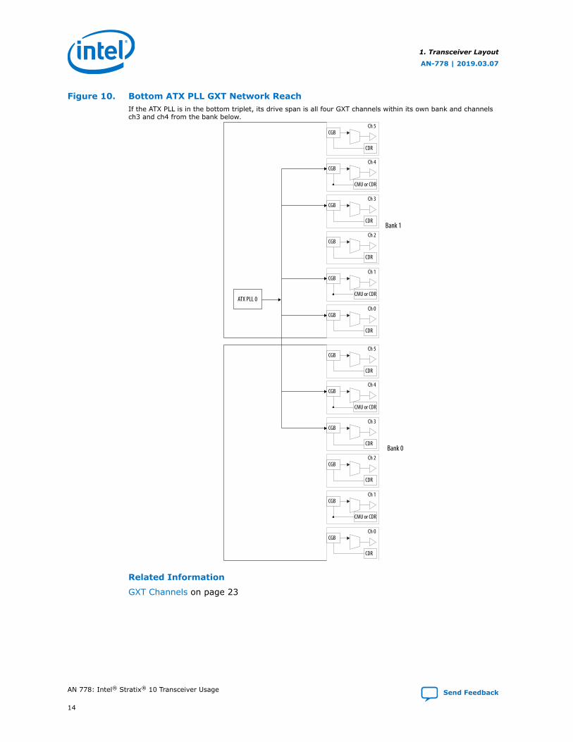
Figure 10. Bottom ATX PLL GXT Network ReachIf the ATX PLL is in the bottom triplet, its drive span is all four GXT channels within its own bank and channelsch3 and ch4 from the bank below.
CMU or CDR
CGBCh 4
CDR
CGBCh 3
CDR
CGBCh 2
CGBCh 1
CDR
CGBCh 0
CDR
CGBCh 5
CMU or CDR
CMU or CDR
CGBCh 4
CDR
CGBCh 3
CDR
CGBCh 2
CGBCh 1
CDR
CGBCh 0
CDR
CGBCh 5
CMU or CDR
ATX PLL 0
Bank 1
Bank 0
Related Information
GXT Channels on page 23
1. Transceiver Layout
AN-778 | 2019.03.07
AN 778: Intel® Stratix® 10 Transceiver Usage Send Feedback
14
1.1.4. Calibration
The transceiver is calibrated at device power on. The OSC_CLK_1 signal is used fordevice configuration and by transceiver calibration logic. OSC_CLK_1 must be drivenby a free running 25 MHz, 100 MHz, or 125 MHz clock source if the transceiver tilesare used. The internal FPGA oscillator cannot be used for transceiver calibration.
The clock source must be stable at FPGA device configuration and should continue torun during device operation.
1. Transceiver Layout
AN-778 | 2019.03.07
Send Feedback AN 778: Intel® Stratix® 10 Transceiver Usage
15
2. Tile Architecture Constraints
2.1. Transceiver Channel Placement
The Intel Stratix 10 product family introduces several transceiver tile variants tosupport a wide variety of protocol implementations.
Table 3. Channel TypesThere are a total of 24 channels available per tile. You can configure them as either GX channels or as acombination of GX and (up to 16) GXT channels as long as the total does not exceed 24. You can use a GXTchannel as a GX channel, but it would be subject to all of the GX channel placement constraints.
Feature L-Tile Transceivers H-Tile Transceivers E-Tile Transceivers
Maximum Datarate(Chip-to-chip)
GX (2)—17.4 Gbps
GX—17.4 GbpsGXT—28.3 Gbps
GXE—57.8 Gbps PulseAmplitude Modulation
(PAM-4)
GXE—28.9 Gbps Non-Return to Zero (NRZ)
GXT (2)—26.6 Gbps
Maximum Datarate(Backplane)
GX and GXT—12.5Gbps
Related Information
L-Tile/H-Tile Building Blocks
2.1.1. Possible Combinations of GX and GXT Channels
This section describes the possible combination of GX and GXT channels for L-Tile ES1and L-Tile/H-Tile.
Related Information
ATX PLL Usage Model When Driving GXT Channels on page 32
2.1.1.1. Possible Combinations of GX and GXT Channels in H-Tile
Table 4. Combination 1: 4 GXT and 2 GX Channels
Channel Type Number of Channels perBank
Channel Capability for H-Tile
Chip-to-Chip Backplane
GX 2 12.5 Gbps N/A
GXT (3) 4 28.3 Gbps 28.3 Gbps
(2) Refer to the L-Tile/H-Tile Building Blocks section for further descriptions of GX and GXTchannels.
(3) If you use GXT channel data rates, the VCCR_GXB and VCCT_GXB voltages must be set to1.12 V.
AN-778 | 2019.03.07
Send Feedback
Intel Corporation. All rights reserved. Intel, the Intel logo, Altera, Arria, Cyclone, Enpirion, MAX, Nios, Quartusand Stratix words and logos are trademarks of Intel Corporation or its subsidiaries in the U.S. and/or othercountries. Intel warrants performance of its FPGA and semiconductor products to current specifications inaccordance with Intel's standard warranty, but reserves the right to make changes to any products and servicesat any time without notice. Intel assumes no responsibility or liability arising out of the application or use of anyinformation, product, or service described herein except as expressly agreed to in writing by Intel. Intelcustomers are advised to obtain the latest version of device specifications before relying on any publishedinformation and before placing orders for products or services.*Other names and brands may be claimed as the property of others.
ISO9001:2015Registered

Figure 11. Example Combination 1: 4 GXT and 2 GX Channels
ch0
ch1ch2ch3ch4ch5
Bank
fPLL
fPLL
ATX PLL
ATX PLLREFCLK0
REFCLK1
GXT channel
GX channel
Note:You cannot use ATX PLL for GX channels when using more than 2 GXT channels per bank
Table 5. Combination 2: 3 GXT and 3 GX Channels
Channel Type Number of Channels perBank
Channel Capability for H-Tile
Chip-to-Chip Backplane
GX 3 12.5 Gbps N/A
GXT (3) 3 28.3 Gbps 28.3 Gbps
Figure 12. Example Combination 2: 3 GXT and 3 GX Channels
ch0
ch1ch2ch3ch4ch5
Bank
fPLL
fPLL
ATX PLL
ATX PLLREFCLK0
REFCLK1
GXT channel
GX channel
Note:You cannot use ATX PLL for GX channels when using more than 2 GXT channels per bank
Table 6. Combination 3: 2 GXT and 4 GX Channels
Channel Type Number of Channels perBank
Channel Capability for H-Tile
Chip-to-Chip Backplane
GX 4 12.5 Gbps N/A
GXT (3) 2 28.3 Gbps 28.3 Gbps
2. Tile Architecture Constraints
AN-778 | 2019.03.07
Send Feedback AN 778: Intel® Stratix® 10 Transceiver Usage
17
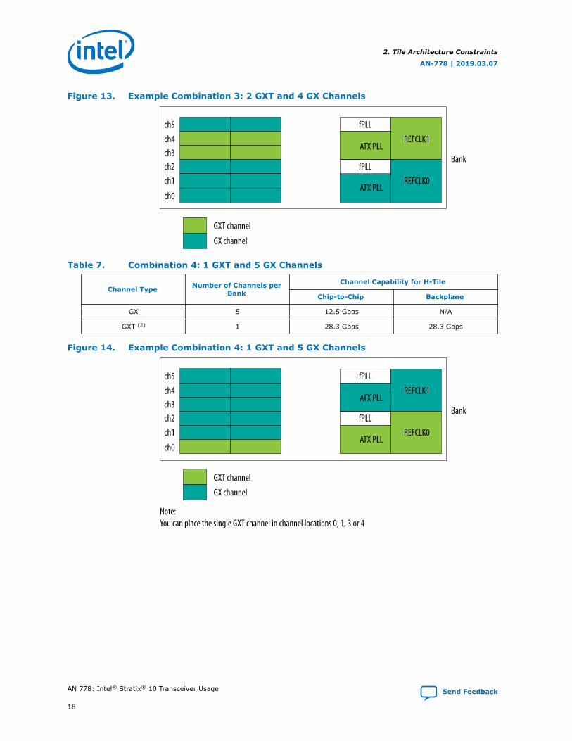
Figure 13. Example Combination 3: 2 GXT and 4 GX Channels
ch0
ch1ch2ch3ch4ch5
Bank
fPLL
fPLL
ATX PLL
ATX PLLREFCLK0
REFCLK1
GXT channel
GX channel
Table 7. Combination 4: 1 GXT and 5 GX Channels
Channel Type Number of Channels perBank
Channel Capability for H-Tile
Chip-to-Chip Backplane
GX 5 12.5 Gbps N/A
GXT (3) 1 28.3 Gbps 28.3 Gbps
Figure 14. Example Combination 4: 1 GXT and 5 GX Channels
ch0
ch1ch2ch3ch4ch5
Bank
fPLL
fPLL
ATX PLL
ATX PLLREFCLK0
REFCLK1
GXT channel
GX channel
Note:You can place the single GXT channel in channel locations 0, 1, 3 or 4
2. Tile Architecture Constraints
AN-778 | 2019.03.07
AN 778: Intel® Stratix® 10 Transceiver Usage Send Feedback
18
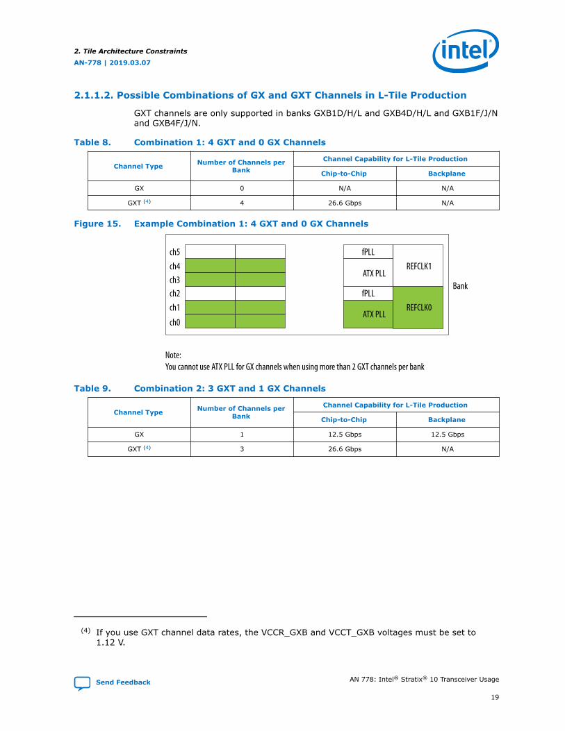
2.1.1.2. Possible Combinations of GX and GXT Channels in L-Tile Production
GXT channels are only supported in banks GXB1D/H/L and GXB4D/H/L and GXB1F/J/Nand GXB4F/J/N.
Table 8. Combination 1: 4 GXT and 0 GX Channels
Channel Type Number of Channels perBank
Channel Capability for L-Tile Production
Chip-to-Chip Backplane
GX 0 N/A N/A
GXT (4) 4 26.6 Gbps N/A
Figure 15. Example Combination 1: 4 GXT and 0 GX Channels
ch0
ch1ch2ch3ch4ch5
Bank
fPLL
fPLL
ATX PLL
ATX PLLREFCLK0
REFCLK1
Note:You cannot use ATX PLL for GX channels when using more than 2 GXT channels per bank
Table 9. Combination 2: 3 GXT and 1 GX Channels
Channel Type Number of Channels perBank
Channel Capability for L-Tile Production
Chip-to-Chip Backplane
GX 1 12.5 Gbps 12.5 Gbps
GXT (4) 3 26.6 Gbps N/A
(4) If you use GXT channel data rates, the VCCR_GXB and VCCT_GXB voltages must be set to1.12 V.
2. Tile Architecture Constraints
AN-778 | 2019.03.07
Send Feedback AN 778: Intel® Stratix® 10 Transceiver Usage
19

Figure 16. Example Combination 2: 3 GXT and 1 GX Channels
ch0
ch1ch2ch3ch4ch5
Bank
fPLL
fPLL
ATX PLL
ATX PLLREFCLK0
REFCLK1
GXT channel
GX channel
Note:You cannot use ATX PLL for GX channels when using more than 2 GXT channels per bank
Table 10. Combination 3: 2 GXT and 2 GX Channels
Channel Type Number of Channels perBank
Channel Capability for L-Tile Production
Chip-to-Chip Backplane
GX 2 12.5 Gbps 12.5 Gbps
GXT (4) 2 26.6 Gbps N/A
Figure 17. Example Combination 3: 2 GXT and 2 GX Channels
ch0
ch1ch2ch3ch4ch5
Bank
fPLL
fPLL
ATX PLL
ATX PLLREFCLK0
REFCLK1
GXT channel
GX channel
Table 11. Combination 4: 1 GXT and 3 GX Channels
Channel Type Number of Channels perBank
Channel Capability for L-Tile Production
Chip-to-Chip Backplane
GX 3 12.5 Gbps 12.5 Gbps
GXT (4) 1 26.6 Gbps N/A
2. Tile Architecture Constraints
AN-778 | 2019.03.07
AN 778: Intel® Stratix® 10 Transceiver Usage Send Feedback
20
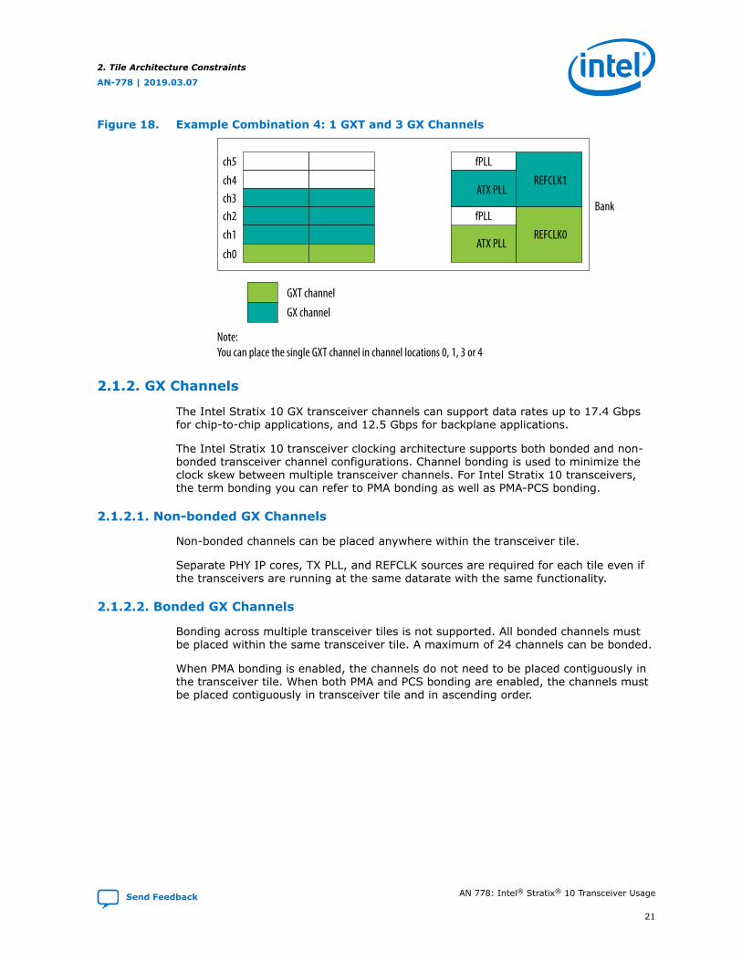
Figure 18. Example Combination 4: 1 GXT and 3 GX Channels
ch0
ch1ch2ch3ch4ch5
Bank
fPLL
fPLL
ATX PLL
ATX PLLREFCLK0
REFCLK1
GXT channel
GX channel
Note:You can place the single GXT channel in channel locations 0, 1, 3 or 4
2.1.2. GX Channels
The Intel Stratix 10 GX transceiver channels can support data rates up to 17.4 Gbpsfor chip-to-chip applications, and 12.5 Gbps for backplane applications.
The Intel Stratix 10 transceiver clocking architecture supports both bonded and non-bonded transceiver channel configurations. Channel bonding is used to minimize theclock skew between multiple transceiver channels. For Intel Stratix 10 transceivers,the term bonding you can refer to PMA bonding as well as PMA-PCS bonding.
2.1.2.1. Non-bonded GX Channels
Non-bonded channels can be placed anywhere within the transceiver tile.
Separate PHY IP cores, TX PLL, and REFCLK sources are required for each tile even ifthe transceivers are running at the same datarate with the same functionality.
2.1.2.2. Bonded GX Channels
Bonding across multiple transceiver tiles is not supported. All bonded channels mustbe placed within the same transceiver tile. A maximum of 24 channels can be bonded.
When PMA bonding is enabled, the channels do not need to be placed contiguously inthe transceiver tile. When both PMA and PCS bonding are enabled, the channels mustbe placed contiguously in transceiver tile and in ascending order.
2. Tile Architecture Constraints
AN-778 | 2019.03.07
Send Feedback AN 778: Intel® Stratix® 10 Transceiver Usage
21

Figure 19. x4 ConfigurationThe figure below shows a way of placing 4 bonded channels. In this case, the logical PCS Master Channelnumber 2 must be specified as Physical channel 4 of bank 0.
CH5
CH4
CH3
CH2
CH1
CH0
CH5
CH4
CH3
CH2
CH1
CH0
Data CH
fPLL
ATXPLL
fPLL
ATXPLL
fPLL
ATXPLL
fPLL
ATXPLL
LogicalChannel
PhysicalChannel
0
1
Transceiver bank 1
Transceiver bank 0
2
3
Data CH
Master CGB
Master CGB
Master CH Master CGB
Master CGB
Data CH
2. Tile Architecture Constraints
AN-778 | 2019.03.07
AN 778: Intel® Stratix® 10 Transceiver Usage Send Feedback
22
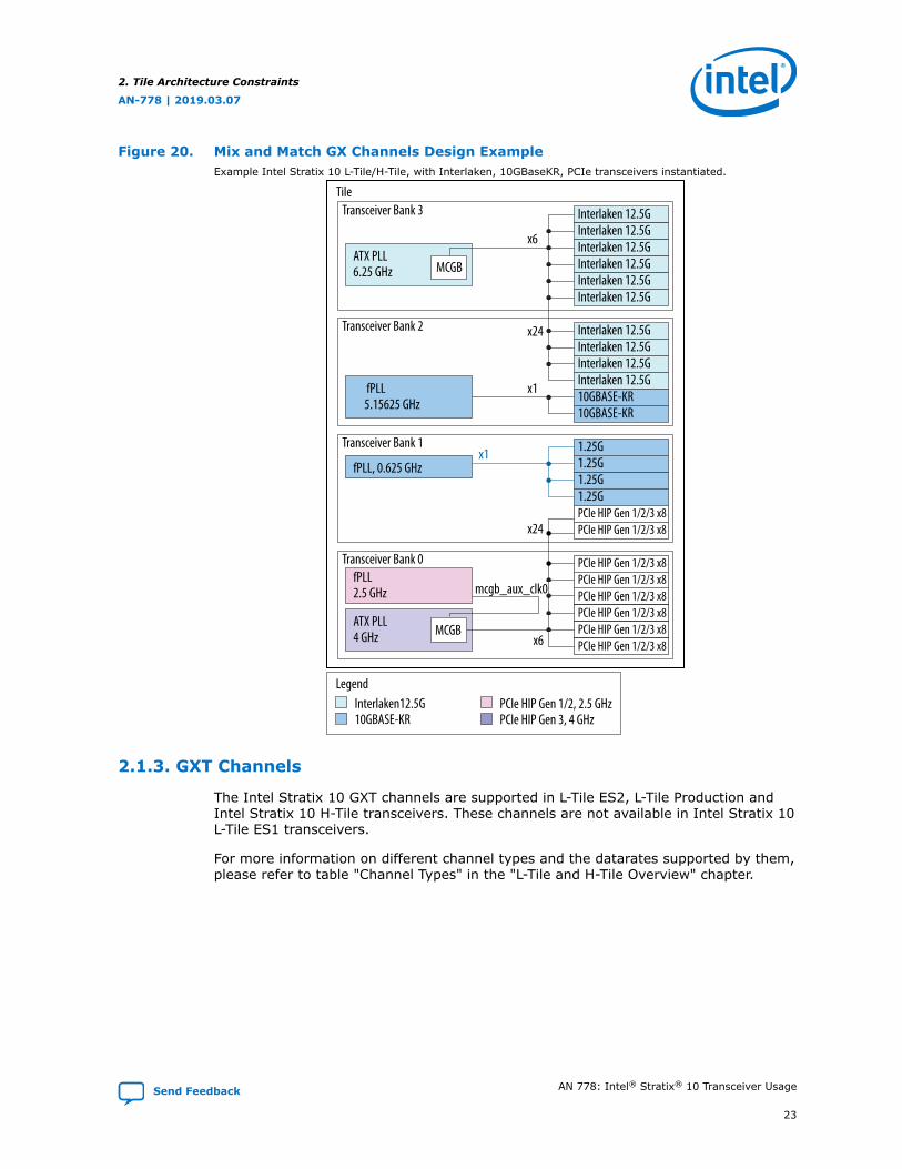
Figure 20. Mix and Match GX Channels Design ExampleExample Intel Stratix 10 L-Tile/H-Tile, with Interlaken, 10GBaseKR, PCIe transceivers instantiated.
Transceiver Bank 0
ATX PLL4 GHz
Transceiver Bank 1
fPLL, 0.625 GHz
Transceiver Bank 2
fPLL5.15625 GHz
Interlaken 12.5G
1.25G
Interlaken 12.5GInterlaken 12.5GInterlaken 12.5GInterlaken 12.5GInterlaken 12.5G
Interlaken 12.5GInterlaken 12.5GInterlaken 12.5GInterlaken 12.5G10GBASE-KR10GBASE-KR
1.25G1.25G
1.25GPCIe HIP Gen 1/2/3 x8PCIe HIP Gen 1/2/3 x8
PCIe HIP Gen 1/2/3 x8
PCIe HIP Gen 1/2/3 x8PCIe HIP Gen 1/2/3 x8
PCIe HIP Gen 1/2/3 x8PCIe HIP Gen 1/2/3 x8PCIe HIP Gen 1/2/3 x8
Transceiver Bank 3
ATX PLL6.25 GHz MCGB
x24
x6
x1
x6MCGB
fPLL2.5 GHz mcgb_aux_clk0
x1
Interlaken12.5G10GBASE-KR
LegendPCIe HIP Gen 1/2, 2.5 GHzPCIe HIP Gen 3, 4 GHz
Tile
x24
2.1.3. GXT Channels
The Intel Stratix 10 GXT channels are supported in L-Tile ES2, L-Tile Production andIntel Stratix 10 H-Tile transceivers. These channels are not available in Intel Stratix 10L-Tile ES1 transceivers.
For more information on different channel types and the datarates supported by them,please refer to table "Channel Types" in the "L-Tile and H-Tile Overview" chapter.
2. Tile Architecture Constraints
AN-778 | 2019.03.07
Send Feedback AN 778: Intel® Stratix® 10 Transceiver Usage
23

Figure 21. Intel Stratix 10 L-Tile GXT Channel Location
CH5CH4CH3CH2CH1CH0
GXT(1)
GXT(1)GXT(1)
ATXfPLL
ATXfPLL
x1/x6
GXBz_TX/RX_CH5GXBz_TX/RX_CH4GXBz_TX/RX_CH3GXBz_TX/RX_CH2GXBz_TX/RX_CH1GXBz_TX/RX_CH0
REFCLK_GXBz_CHT
REFCLK_GXBz_CHB
Notes:1. Refer to table “Channel Types” for GXT channel capabilities.
CH5CH4CH3CH2CH1CH0
ATXfPLL
ATXfPLL
x1/x6
GXBy_TX/RX_CH5GXBy_TX/RX_CH4GXBy_TX/RX_CH3GXBy_TX/RX_CH2GXBy_TX/RX_CH1GXBy_TX/RX_CH0
REFCLK_GXBy_CHT
REFCLK_GXBy_CHB
CH5CH4CH3CH2CH1CH0
GXT(1)GXT(1)
GXT(1)GXT(1)
ATXfPLL
ATXfPLL
x1/x6
GXBx_TX/RX_CH5GXBx_TX/RX_CH4GXBx_TX/RX_CH3GXBx_TX/RX_CH2GXBx_TX/RX_CH1GXBx_TX/RX_CH0
REFCLK_GXBx_CHT
REFCLK_GXBx_CHB
CH5CH4CH3CH2CH1CH0
ATXfPLL
ATXfPLL
x1/x6
GXBw_TX/RX_CH5GXBw_TX/RX_CH4GXBw_TX/RX_CH3GXBw_TX/RX_CH2GXBw_TX/RX_CH1GXBw_TX/RX_CH0
REFCLK_GXBw_CHT
REFCLK_GXBw_CHB
x24
PCIeHard IP
x16
Tile
EMIB
Transceiver ChannelTransceiver Channel and CMU PLLPCIe Hard IP x8 Maximum Lanes Supported on EAP and Initial ES
6-Pack Separation within Tile(x1/x6 Lines Do Not Cross These Lines)
GXBwGXB1CGXB1GGXB1KGXB4CGXB4GGXB4K
GXBxGXB1DGXB1HGXB1LGXB4DGXB4HGXB4L
GXByGXB1EGXB1I
GXB1MGXB4EGXB4I
GXB4M
GXBzGXB1FGXB1JGXB1NGXB4FGXB4JGXB4N
Tile Bottom LeftTile Middle LeftTile Top LeftTile Bottom RightTile Middle RightTile Top Right
GXT(1)
2. Tile Architecture Constraints
AN-778 | 2019.03.07
AN 778: Intel® Stratix® 10 Transceiver Usage Send Feedback
24
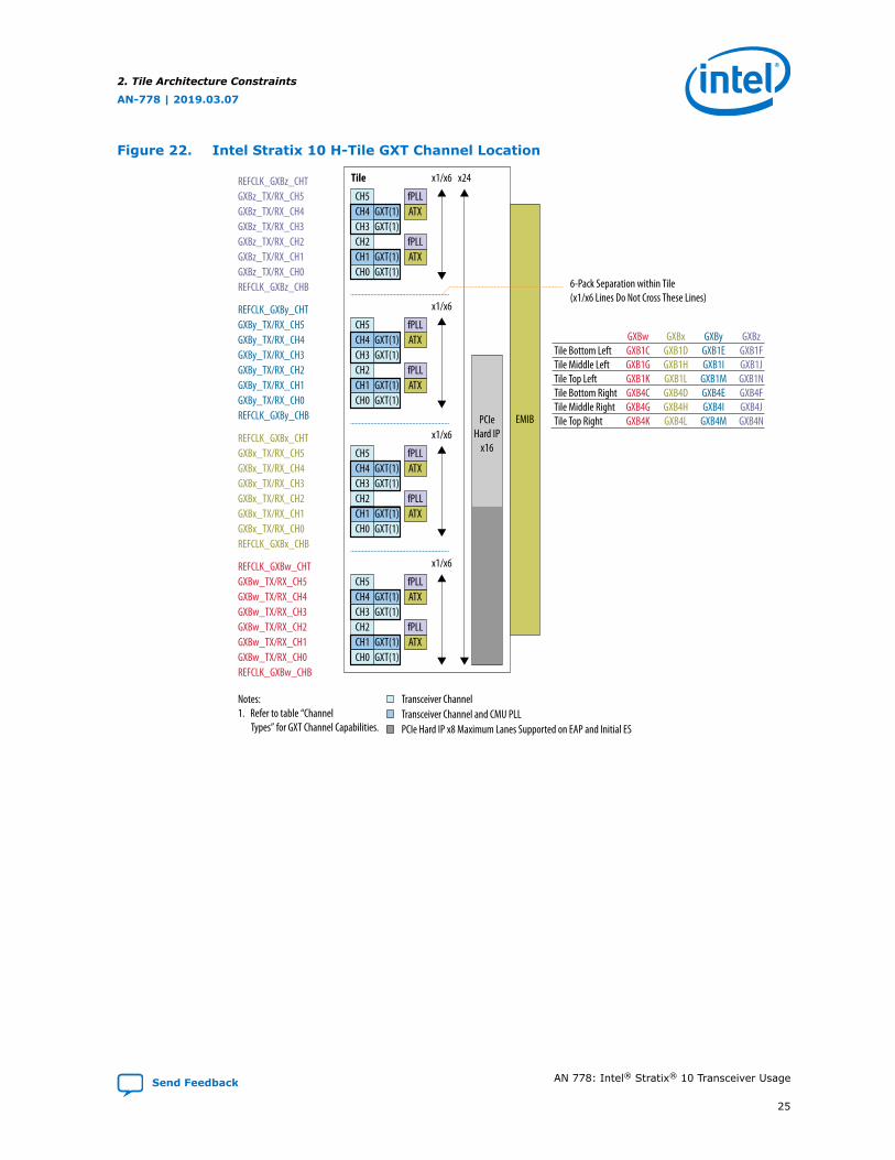
Figure 22. Intel Stratix 10 H-Tile GXT Channel Location
CH5CH4CH3CH2CH1CH0
GXT(1)GXT(1)
GXT(1)GXT(1)
ATXfPLL
ATXfPLL
x1/x6
GXBz_TX/RX_CH5GXBz_TX/RX_CH4GXBz_TX/RX_CH3GXBz_TX/RX_CH2GXBz_TX/RX_CH1GXBz_TX/RX_CH0
REFCLK_GXBz_CHT
REFCLK_GXBz_CHB
Notes:1. Refer to table “Channel Types” for GXT Channel Capabilities.
CH5CH4CH3CH2CH1CH0
GXT(1)GXT(1)
GXT(1)GXT(1)
ATXfPLL
ATXfPLL
x1/x6
GXBy_TX/RX_CH5GXBy_TX/RX_CH4GXBy_TX/RX_CH3GXBy_TX/RX_CH2GXBy_TX/RX_CH1GXBy_TX/RX_CH0
REFCLK_GXBy_CHT
REFCLK_GXBy_CHB
CH5CH4CH3CH2CH1CH0
GXT(1)GXT(1)
GXT(1)GXT(1)
ATXfPLL
ATXfPLL
x1/x6
GXBx_TX/RX_CH5GXBx_TX/RX_CH4GXBx_TX/RX_CH3GXBx_TX/RX_CH2GXBx_TX/RX_CH1GXBx_TX/RX_CH0
REFCLK_GXBx_CHT
REFCLK_GXBx_CHB
CH5CH4CH3CH2CH1CH0
GXT(1)GXT(1)
GXT(1)GXT(1)
ATXfPLL
ATXfPLL
x1/x6
GXBw_TX/RX_CH5GXBw_TX/RX_CH4GXBw_TX/RX_CH3GXBw_TX/RX_CH2GXBw_TX/RX_CH1GXBw_TX/RX_CH0
REFCLK_GXBw_CHT
REFCLK_GXBw_CHB
x24
PCIeHard IP
x16
Tile
EMIB
Transceiver ChannelTransceiver Channel and CMU PLLPCIe Hard IP x8 Maximum Lanes Supported on EAP and Initial ES
6-Pack Separation within Tile(x1/x6 Lines Do Not Cross These Lines)
GXBwGXB1CGXB1GGXB1KGXB4CGXB4GGXB4K
GXBxGXB1DGXB1HGXB1LGXB4DGXB4HGXB4L
GXByGXB1EGXB1I
GXB1MGXB4EGXB4I
GXB4M
GXBzGXB1FGXB1JGXB1NGXB4FGXB4JGXB4N
Tile Bottom LeftTile Middle LeftTile Top LeftTile Bottom RightTile Middle RightTile Top Right
2. Tile Architecture Constraints
AN-778 | 2019.03.07
Send Feedback AN 778: Intel® Stratix® 10 Transceiver Usage
25

Figure 23. GXT and GX Channel Placement Example for L-Tile
ch0
ch1ch2ch3ch4ch5
L-Tile
ILKN (C2C)ILKN (C2C)
ILKN (C2C)
ILKN (C2C)
Bank 3
ch0
ch1ch2ch3ch4ch5
ch0
ch1ch2ch3ch4ch5
ch0
ch1ch2ch3ch4ch5
fPLL
fPLL
ATX PLL
ATX PLLREFCLK0
REFCLK1
fPLL
fPLL
ATX PLL
ATX PLLREFCLK0
REFCLK1
fPLL
fPLL
ATX PLL
ATX PLLREFCLK0
REFCLK1
fPLL
fPLL
ATX PLL
ATX PLLREFCLK0
REFCLK1
= 26.6 Gbps channel
= 12.5 Gbps channel
PCIe Hard IP(BP)
= PCIe Gen3 x16
Bank 2
Bank 1
Bank 0
= BackplaneBPC2C = Chip-to-chip
JESD (C2C)
JESD (C2C)
2. Tile Architecture Constraints
AN-778 | 2019.03.07
AN 778: Intel® Stratix® 10 Transceiver Usage Send Feedback
26

Figure 24. GXT and GX Channel Placement Example for H-Tile
ch0
ch1ch2ch3ch4ch5
H-Tile
ILKN (C2C)ILKN (C2C)
ILKN (C2C)
ILKN (C2C)
Bank 3
ch0
ch1ch2ch3ch4ch5
ILKN (C2C)ILKN (C2C)
ILKN (C2C)
ILKN (C2C)
ch0
ch1ch2ch3ch4ch5
ILKN (C2C)ILKN (C2C)
ILKN (C2C)
ILKN (C2C)
ch0
ch1ch2ch3ch4ch5
JESD (C2C)JESD (C2C)
JESD (C2C)
JESD (C2C)
JESD (C2C)
fPLL
fPLL
ATX PLL
ATX PLLREFCLK0
REFCLK1
fPLL
fPLL
ATX PLL
ATX PLLREFCLK0
REFCLK1
fPLL
fPLL
ATX PLL
ATX PLLREFCLK0
REFCLK1
fPLL
fPLL
ATX PLL
ATX PLLREFCLK0
REFCLK1
= 28.3 Gbps channel
= 12.5 Gbps channel
Bank 2
Bank 1
Bank 0
= Chip-to-chipC2C
2. Tile Architecture Constraints
AN-778 | 2019.03.07
Send Feedback AN 778: Intel® Stratix® 10 Transceiver Usage
27
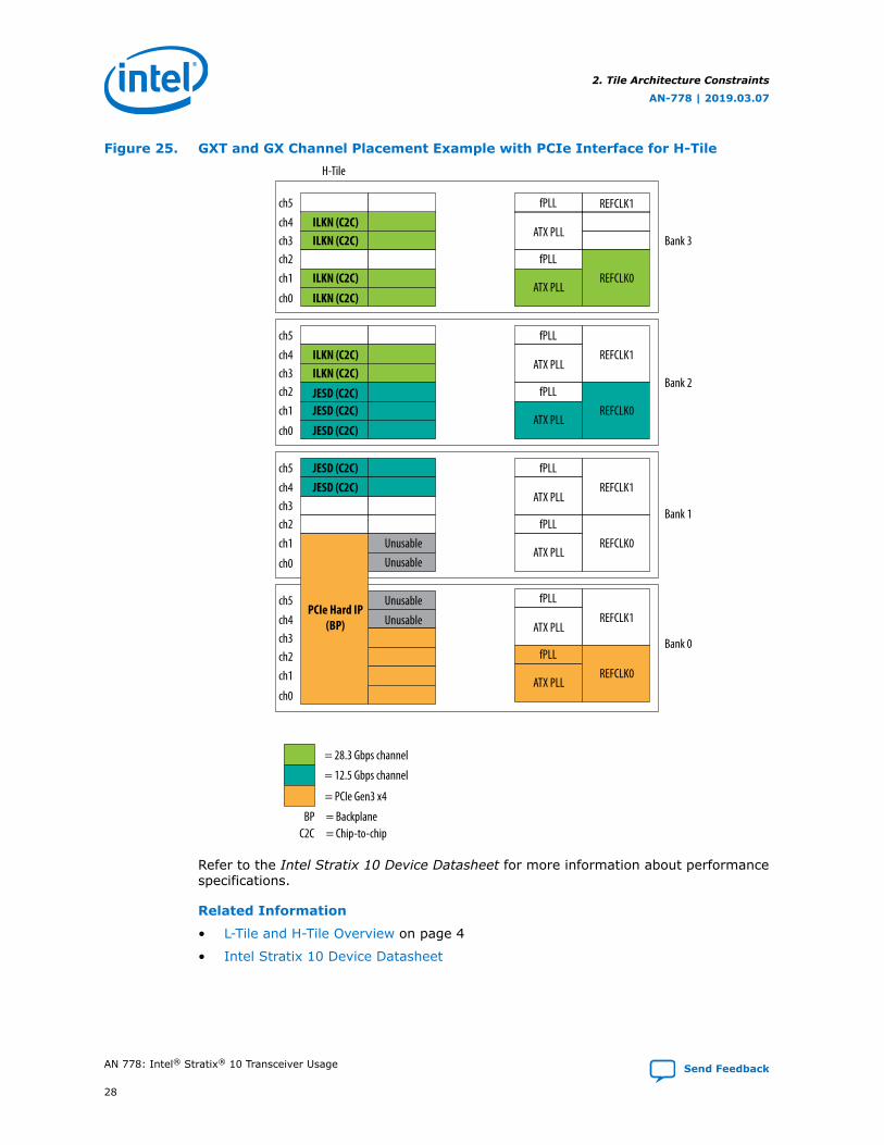
Figure 25. GXT and GX Channel Placement Example with PCIe Interface for H-Tile
ch0
ch1ch2ch3ch4ch5
H-Tile
ILKN (C2C)ILKN (C2C)
ILKN (C2C)
ILKN (C2C)
Bank 3
ch0
ch1ch2ch3ch4ch5
ILKN (C2C)ILKN (C2C)
JESD (C2C)
JESD (C2C)
ch0
ch1ch2ch3ch4ch5
ch0
ch1ch2ch3ch4ch5
fPLL
fPLL
ATX PLL
ATX PLLREFCLK0
REFCLK1
fPLL
fPLL
ATX PLL
ATX PLLREFCLK0
REFCLK1
fPLL
fPLL
ATX PLL
ATX PLLREFCLK0
REFCLK1
fPLL
fPLL
ATX PLL
ATX PLLREFCLK0
REFCLK1
= 28.3 Gbps channel
= 12.5 Gbps channel
UnusableUnusable
Unusable
UnusablePCIe Hard IP
(BP)
JESD (C2C)JESD (C2C)
JESD (C2C)
= PCIe Gen3 x4
Bank 2
Bank 1
Bank 0
= BackplaneBPC2C = Chip-to-chip
Refer to the Intel Stratix 10 Device Datasheet for more information about performancespecifications.
Related Information
• L-Tile and H-Tile Overview on page 4
• Intel Stratix 10 Device Datasheet
2. Tile Architecture Constraints
AN-778 | 2019.03.07
AN 778: Intel® Stratix® 10 Transceiver Usage Send Feedback
28

2.1.4. Reference Clock Guidelines for L-Tile and H-Tile
The transmitter PLL and the clock data recovery (CDR) block need an input referenceclock source to generate the clocks required for transceiver operation. The inputreference clock must be stable and free-running at device power-up for proper PLLcalibrations.
Intel Stratix 10 transceiver PLLs have five possible input reference clock sources,depending on jitter requirements:
• Dedicated reference clock pins
• Receiver input pins
• Reference clock network
• PLL cascade output (fPLL only)
• Core clock network (fPLL only)
Note: Each core clock network reference clock pin cannot drive fPLLs located on multipleL/H-Tiles
Intel recommends using the dedicated reference clock pins and the reference clocknetwork for the best jitter performance.
For the best jitter performance, Intel recommends placing the reference clock as closeas possible to the transmitter PLL. The following protocols require the reference clockto be placed in same bank as the transmitter PLL:
• OTU2e, OTU2, OC-192 and 10G PON
• 6G and 12G SDI
Note: For optimum performance of GXT channel, the reference clock of transmitter PLL isrecommended to be from a dedicated reference clock pin in the same bank.
Figure 26. Input Reference Clock Sources
Dedicated refclk pin
RX pin 4
Note : (1) Any RX pin in the same bank can be used as an input reference clock.
RX pin 0
Reference ClockNetwork
Serial Clock
FractionalPLL
ATX PLL, Channel PLL
(CMU PLL/CDR), or fPLL
Input Reference
Clock
(2)
(2) The output of another PLL can be used as an input reference clock source during PLL cascading. Intel Stratix 10 transceivers support fPLL to fPLL and ATX PLL to fPLL cascading. Refer to “PLL Cascading Clock Network” for more details on PLL cascading.
(1)
(fPLL)Core Clock (3)
RX pin 5
(3) Core Clock present only for fPLL.
Note: In Intel Stratix 10 devices, the FPGA fabric core clock network can be used as an inputreference source for fPLL only.
2. Tile Architecture Constraints
AN-778 | 2019.03.07
Send Feedback AN 778: Intel® Stratix® 10 Transceiver Usage
29
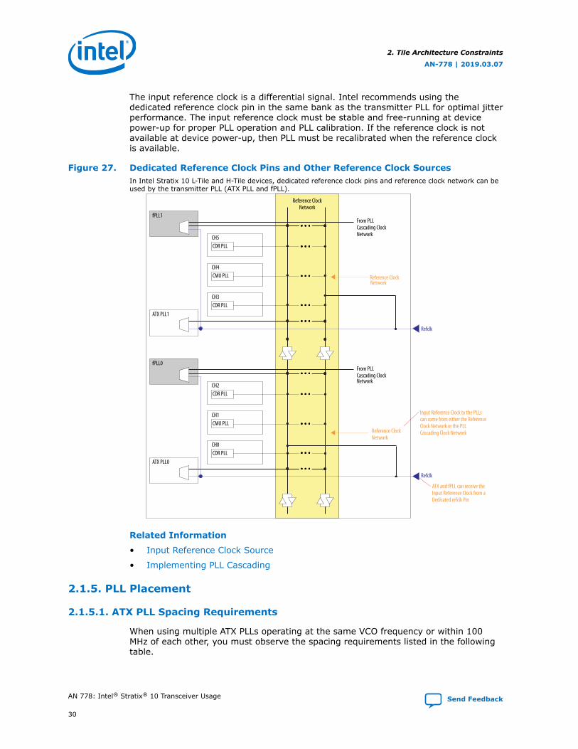
The input reference clock is a differential signal. Intel recommends using thededicated reference clock pin in the same bank as the transmitter PLL for optimal jitterperformance. The input reference clock must be stable and free-running at devicepower-up for proper PLL operation and PLL calibration. If the reference clock is notavailable at device power-up, then PLL must be recalibrated when the reference clockis available.
Figure 27. Dedicated Reference Clock Pins and Other Reference Clock SourcesIn Intel Stratix 10 L-Tile and H-Tile devices, dedicated reference clock pins and reference clock network can beused by the transmitter PLL (ATX PLL and fPLL).
Refclk
CH5
CMU PLLCH4
CDR PLLCH3
fPLL1
ATX PLL1
CDR PLL
From PLL Cascading ClockNetwork
Refclk
CH2
CMU PLLCH1
CDR PLLCH0
fPLL0
ATX PLL0
CDR PLL
Reference ClockNetwork
Reference ClockNetwork
Reference ClockNetwork
Input Reference Clock to the PLLscan come from either the ReferenceClock Network or the PLL Cascading Clock Network
ATX and fPLL can receive the Input Reference Clock from a Dedicated refclk Pin
From PLL Cascading ClockNetwork
Related Information
• Input Reference Clock Source
• Implementing PLL Cascading
2.1.5. PLL Placement
2.1.5.1. ATX PLL Spacing Requirements
When using multiple ATX PLLs operating at the same VCO frequency or within 100MHz of each other, you must observe the spacing requirements listed in the followingtable.
2. Tile Architecture Constraints
AN-778 | 2019.03.07
AN 778: Intel® Stratix® 10 Transceiver Usage Send Feedback
30
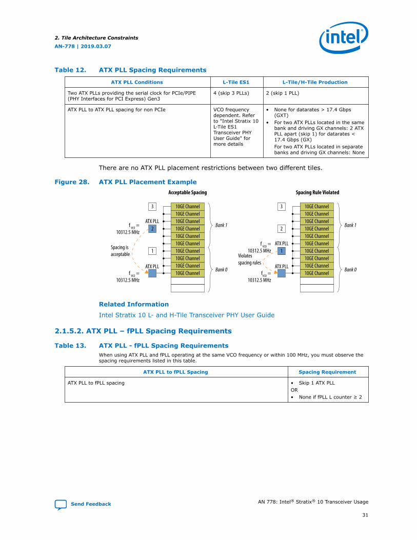
Table 12. ATX PLL Spacing Requirements
ATX PLL Conditions L-Tile ES1 L-Tile/H-Tile Production
Two ATX PLLs providing the serial clock for PCIe/PIPE(PHY Interfaces for PCI Express) Gen3
4 (skip 3 PLLs) 2 (skip 1 PLL)
ATX PLL to ATX PLL spacing for non PCIe VCO frequencydependent. Referto "Intel Stratix 10L-Tile ES1Transceiver PHYUser Guide" formore details
• None for datarates > 17.4 Gbps(GXT)
• For two ATX PLLs located in the samebank and driving GX channels: 2 ATXPLL apart (skip 1) for datarates <17.4 Gbps (GX)For two ATX PLLs located in separatebanks and driving GX channels: None
There are no ATX PLL placement restrictions between two different tiles.
Figure 28. ATX PLL Placement Example
10GE Channel10GE Channel10GE Channel10GE Channel10GE Channel10GE Channel10GE Channel10GE Channel10GE Channel10GE Channel
Bank 1
Bank 0
1
3
2
ATX PLL
Acceptable Spacing
f VCO =10312.5 MHz
10GE Channel10GE Channel10GE Channel10GE Channel10GE Channel10GE Channel10GE Channel10GE Channel10GE Channel10GE Channel
Bank 1
Bank 0
1
3
2
ATX PLL
Spacing Rule Violated
fVCO =10312.5 MHz
Spacing is acceptable Violates
spacing rules
f VCO =10312.5 MHz
f VCO =10312.5 MHz
ATX PLL
ATX PLL
Related Information
Intel Stratix 10 L- and H-Tile Transceiver PHY User Guide
2.1.5.2. ATX PLL – fPLL Spacing Requirements
Table 13. ATX PLL - fPLL Spacing RequirementsWhen using ATX PLL and fPLL operating at the same VCO frequency or within 100 MHz, you must observe thespacing requirements listed in this table.
ATX PLL to fPLL Spacing Spacing Requirement
ATX PLL to fPLL spacing • Skip 1 ATX PLLOR• None if fPLL L counter ≥ 2
2. Tile Architecture Constraints
AN-778 | 2019.03.07
Send Feedback AN 778: Intel® Stratix® 10 Transceiver Usage
31
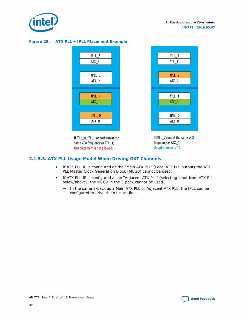
Figure 29. ATX PLL – fPLL Placement Example
fPLL_3ATX_3
fPLL_2ATX_2
fPLL_1ATX_1
fPLL_0ATX_0
fPLL_3ATX_3
fPLL_2ATX_2
fPLL_1ATX_1
fPLL_0ATX_0
If fPLL_0, fPLL1, or both run at the same VCO frequency as ATX_1,this placement is not allowed.
If fPLL_2 runs at the same VCOfrequency as ATX_1,this placement is OK.
2.1.5.3. ATX PLL Usage Model When Driving GXT Channels
• If ATX PLL IP is configured as the “Main ATX PLL” (Local ATX PLL output) the ATXPLL Master Clock Generation Block (MCGB) cannot be used.
• If ATX PLL IP is configured as an “Adjacent ATX PLL” (selecting input from ATX PLLbelow/above), the MCGB in the 3-pack cannot be used.
— In the same 3-pack as a Main ATX PLL or Adjacent ATX PLL, the fPLL can beconfigured to drive the x1 clock lines.
2. Tile Architecture Constraints
AN-778 | 2019.03.07
AN 778: Intel® Stratix® 10 Transceiver Usage Send Feedback
32

Figure 30. Restrictions for ATX PLL GX and MCGB
Local CGB
CDRCH2
Local CGB
CDR/CMUCH1
Local CGB
CDRCH0
fPLL
ATXPLL
MasterCGB
Local CGB
CDRCH5
Local CGB
CDR/CMUCH4
Local CGB
CDRCH3
fPLL
ATXPLL
MasterCGB
Local CGB
CDRCH2
Local CGB
CDR/CMUCH1
Local CGB
CDRCH0
fPLL
ATXPLL
MasterCGB
Local CGB
CDRCH5
Local CGB
CDR/CMUCH4
Local CGB
CDRCH3
fPLL
ATXPLL
MasterCGB
x1 Clock Lines x6 Clock Lines x24 Clock LinesTransceiver
Bank
TransceiverBank
Main ATX PLL
Adjacent ATX PLL
GXT Channels driven by the Main ATX PLL and Adjacent ATX PLL
Related Information
• Using the ATX PLL for GXT Channels
• GXT Implementation Usage Restrictions for ATX PLL GX & MCGB
2.1.5.4. Simplex Channel Merging
You can merge the following logical instances into a single physical channel:
2. Tile Architecture Constraints
AN-778 | 2019.03.07
Send Feedback AN 778: Intel® Stratix® 10 Transceiver Usage
33
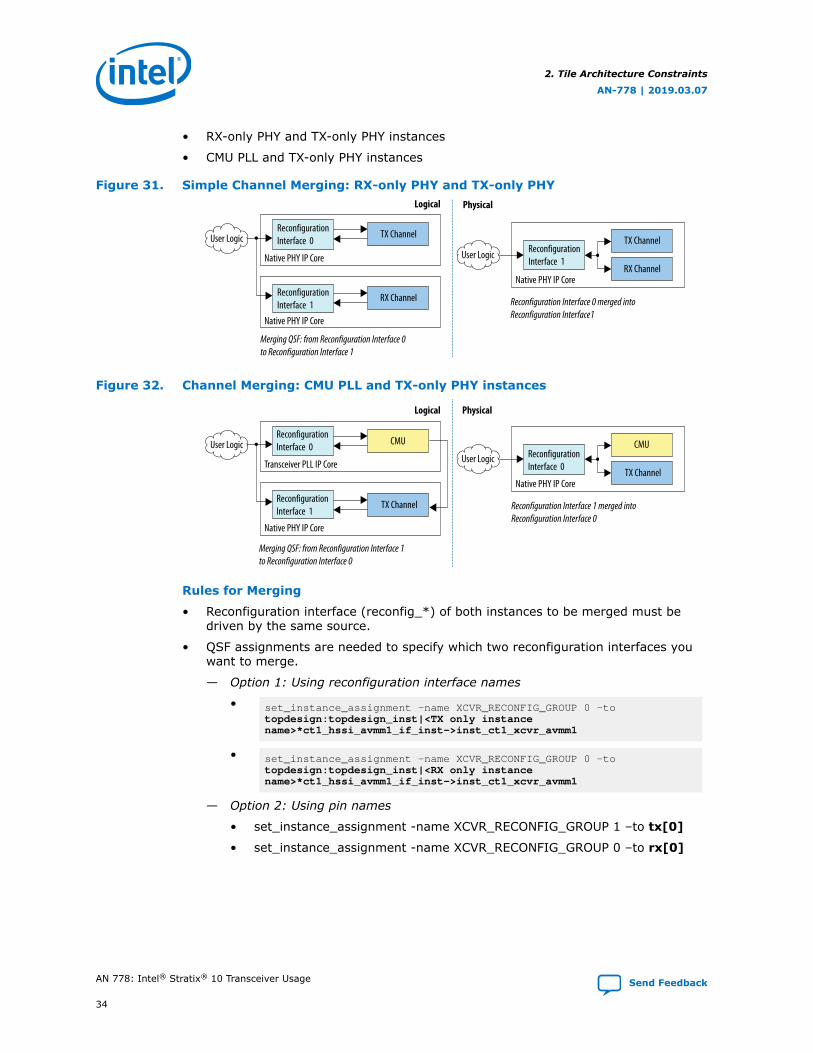
• RX-only PHY and TX-only PHY instances
• CMU PLL and TX-only PHY instances
Figure 31. Simple Channel Merging: RX-only PHY and TX-only PHY
Reconfiguration Interface 0
TX Channel
RX Channel
User Logic
Native PHY IP Core
Native PHY IP Core
Logical
User Logic
Native PHY IP Core
Physical
TX Channel
RX Channel
Reconfiguration Interface 0 merged into Reconfiguration Interface1
Merging QSF: from Reconfiguration Interface 0 to Reconfiguration Interface 1
Reconfiguration Interface 1
Reconfiguration Interface 1
Figure 32. Channel Merging: CMU PLL and TX-only PHY instances
CMU
TX Channel
User Logic
Transceiver PLL IP Core
Native PHY IP Core
Logical
User Logic
Native PHY IP Core
Physical
CMU
TX Channel
Reconfiguration Interface 1 merged into Reconfiguration Interface 0
Merging QSF: from Reconfiguration Interface 1 to Reconfiguration Interface 0
Reconfiguration Interface 0
Reconfiguration Interface 0
Reconfiguration Interface 1
Rules for Merging
• Reconfiguration interface (reconfig_*) of both instances to be merged must bedriven by the same source.
• QSF assignments are needed to specify which two reconfiguration interfaces youwant to merge.
— Option 1: Using reconfiguration interface names
• set_instance_assignment -name XCVR_RECONFIG_GROUP 0 -to topdesign:topdesign_inst|<TX only instance name>*ct1_hssi_avmm1_if_inst->inst_ct1_xcvr_avmm1
• set_instance_assignment -name XCVR_RECONFIG_GROUP 0 -to topdesign:topdesign_inst|<RX only instance name>*ct1_hssi_avmm1_if_inst->inst_ct1_xcvr_avmm1
— Option 2: Using pin names
• set_instance_assignment -name XCVR_RECONFIG_GROUP 1 –to tx[0]
• set_instance_assignment -name XCVR_RECONFIG_GROUP 0 –to rx[0]
2. Tile Architecture Constraints
AN-778 | 2019.03.07
AN 778: Intel® Stratix® 10 Transceiver Usage Send Feedback
34
• The simplex channels cannot be merged if any of the following options are enabledin one or both simplex instances:
— Altera Debug Master Endpoint (ADME)
— Optional reconfiguration logic
— Embedded reconfiguration streamer
— Shared reconfiguration interface
Related Information
Reconfiguration Interface and Dynamic Reconfiguration
2.1.5.5. TX PLL Restrictions when Using PCIe
Intel recommends that the remaining channels of the tile in L-Tile ES1/L-TileProduction (PIPE) are to be driven by ATX PLL if 4 or more channels of PCIe are usedat Gen2 or Gen3 speeds. Using ATX PLL to drive these channels helps achieve betterperformance. Intel Quartus® Prime issues a critical warning if fPLL is used to drive theremaining channels.
2.2. Unsupported Dynamic Reconfiguration Features
The following is a list of the unsupported dynamic reconfiguration features:
• Reconfiguration from a bonded configuration to a non-bonded configuration, orvice versa
• Reconfiguration from a bonded protocol to another bonded protocol
• Reconfiguration from PCIe (with Hard IP) to PCIe (without Hard IP), or non-PCIebonded protocol switching
• Master clock generation block (MCGB) reconfiguration
• Switching between two master CGBs
• Serialization factor changes on bonded channels
• TX PLL switching on bonded channels
2.3. Intel Stratix 10 L-Tile Transceiver to H-Tile TransceiverMigration
All of the L-Tile transceiver constraints apply to H-Tile transceivers as well. The H-Tiletransceivers have no further restrictions than the L-Tile transceivers, with theexception of the GXT channels.
If you plan to use GXT channels in the H-Tile, the VCCR_GXB and VCCT_GXB pins on thattile must be set to 1.12 V.
Note: When migrating from L-Tile to H-Tile transceivers, use the Stratix 10 Early PowerEstimator (EPE) tool to validate your regulator sizing.
The placement constraints for the GXT channels, which are available in L-TileProduction and H-Tile transceivers, are mentioned in the GXT Channels section.
2. Tile Architecture Constraints
AN-778 | 2019.03.07
Send Feedback AN 778: Intel® Stratix® 10 Transceiver Usage
35
Related Information
GXT Channels on page 23
2.4. Thermal Guidelines
Optimal thermal performance can be achieved by reducing the power density withinthe transceiver tile. Placing many high data rate channels next to each other results inhigh power density areas within a tile. Following a general guideline of minimizingpower density results in a less complex, and cheaper cooling solution for the FPGA.
For best thermal performance you can minimize power density by picking transceiverchannel locations early on. Follow these guidelines when placing your transceiverchannels within a tile:
• Spread out channels as much as possible
• If all channels in a tile are used, intersperse low and high data rate channels
• The middle of the tile has the best thermal performance, followed by the bottomand then the top of each tile when looking at the Pin Planner
The latest Intel Stratix 10 Early Power Estimator (EPE) contains a Thermal worksheetto help you determine the impact of transceiver placement on your thermal solutionrequirements. Prior to finalizing your board design you should analyze your transceiverchannel placement using the Intel Stratix 10 EPE to ensure it is thermally optimal.
Note: Contact your local FAE to have Intel run a thermal analysis of your board design afteryou have determined placement of all transceiver channels.
2. Tile Architecture Constraints
AN-778 | 2019.03.07
AN 778: Intel® Stratix® 10 Transceiver Usage Send Feedback
36

3. PCIe Guidelines
3.1. PCIe Hard IP
There is one PCIe Hard IP available per transceiver tile.
3.1.1. Channel Placement for PCIe Hard IP
The PCIe lane 0 is always mapped to ch0 of the transceiver tile. Channel 0 of thetransceiver tile = Bank 0, Channel 0.
The PCIe x1, x2, x4 and x8 configurations always consume a total of eight transceiverchannels.
CvP Support
Only the bottom left transceiver tile supports configuration via protocol (CvP).
Figure 33. Transceiver Channel Usage for PCIe x1, X2, x4, x8 and x16
PCIe Hard IP x1
7 ChannelsUnusable
PCIe x1
PCIe Hard IP x2
6 ChannelsUnusable
PCIe x2
PCIe Hard IP x4
4 ChannelsUnusable
PCIe x4
PCIe Hard IP x8
PCIe x8
PCIe Hard IP x16
PCIe x16
Transceiver Tile Transceiver Tile Transceiver Tile Transceiver Tile Transceiver Tile0 0 0 0 0
15
23 23 23 23 23
8 8 87 7
8
134
1
7
2
7
16 ChannelsUsable
16 ChannelsUsable
16 ChannelsUsable
16 ChannelsUsable
8 ChannelsUsable
16
For L-Tile ES1 and L-Tile Production (PIPE only), any transceiver channel running atdata rate above 6.5 Gbps that shares a tile with an active PCI Express interface thatare Gen2 or Gen3 capable and configured with more than 2 lanes (Gen2/3 x4, x8,x16) may observe momentary bit errors (BER) during a PCI Express rate change event(PCIe link training both up and down, i.e., link down and start of link training ).Transceiver channels that share a tile with active PCI Express interfaces that are onlyGen1 capable are not impacted.
AN-778 | 2019.03.07
Send Feedback
Intel Corporation. All rights reserved. Intel, the Intel logo, Altera, Arria, Cyclone, Enpirion, MAX, Nios, Quartusand Stratix words and logos are trademarks of Intel Corporation or its subsidiaries in the U.S. and/or othercountries. Intel warrants performance of its FPGA and semiconductor products to current specifications inaccordance with Intel's standard warranty, but reserves the right to make changes to any products and servicesat any time without notice. Intel assumes no responsibility or liability arising out of the application or use of anyinformation, product, or service described herein except as expressly agreed to in writing by Intel. Intelcustomers are advised to obtain the latest version of device specifications before relying on any publishedinformation and before placing orders for products or services.*Other names and brands may be claimed as the property of others.
ISO9001:2015Registered
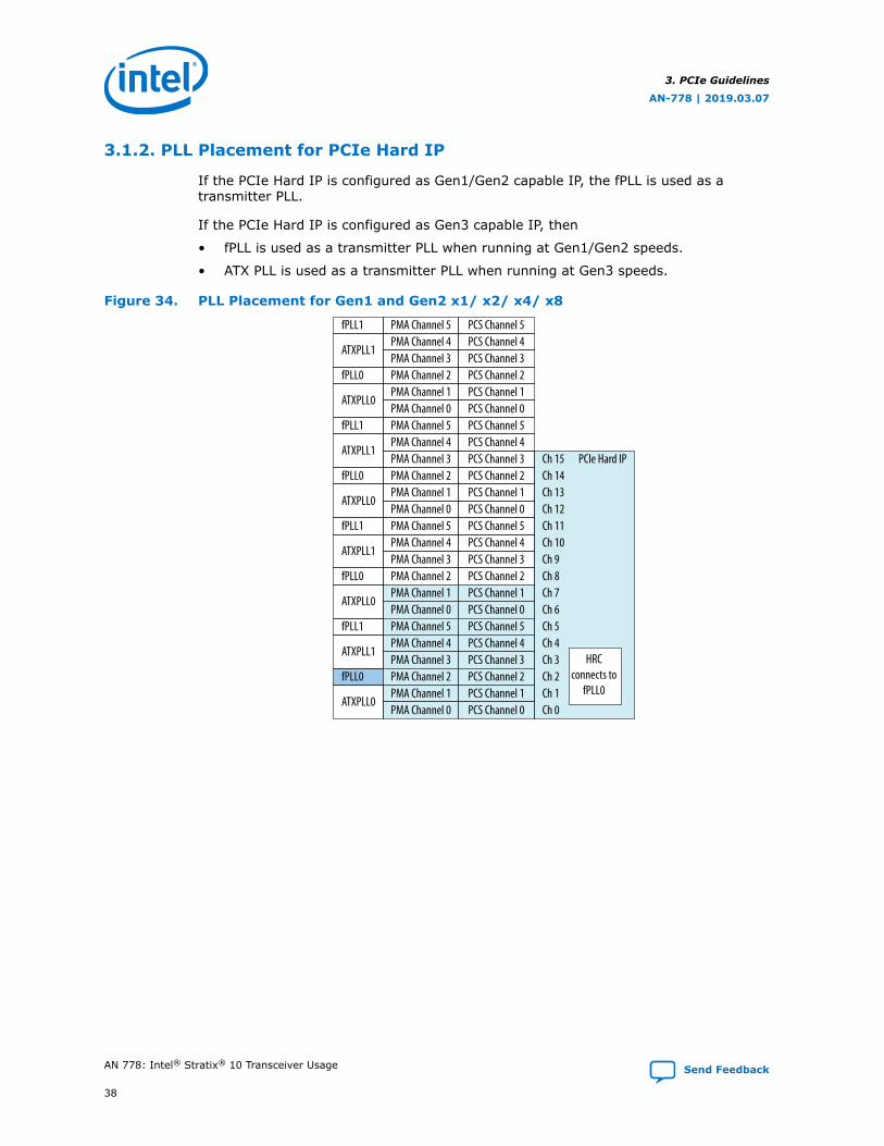
3.1.2. PLL Placement for PCIe Hard IP
If the PCIe Hard IP is configured as Gen1/Gen2 capable IP, the fPLL is used as atransmitter PLL.
If the PCIe Hard IP is configured as Gen3 capable IP, then
• fPLL is used as a transmitter PLL when running at Gen1/Gen2 speeds.
• ATX PLL is used as a transmitter PLL when running at Gen3 speeds.
Figure 34. PLL Placement for Gen1 and Gen2 x1/ x2/ x4/ x8
PMA Channel 5PMA Channel 4PMA Channel 3PMA Channel 2PMA Channel 1PMA Channel 0
PCS Channel 5PCS Channel 4PCS Channel 3PCS Channel 2PCS Channel 1PCS Channel 0
fPLL1
fPLL0
ATXPLL0
ATXPLL1
PMA Channel 5PMA Channel 4PMA Channel 3PMA Channel 2PMA Channel 1PMA Channel 0
PCS Channel 5PCS Channel 4PCS Channel 3PCS Channel 2PCS Channel 1PCS Channel 0
fPLL1
fPLL0
ATXPLL0
ATXPLL1
PMA Channel 5PMA Channel 4PMA Channel 3PMA Channel 2PMA Channel 1PMA Channel 0
PCS Channel 5PCS Channel 4PCS Channel 3PCS Channel 2PCS Channel 1PCS Channel 0
fPLL1
fPLL0
ATXPLL0
ATXPLL1
PMA Channel 5PMA Channel 4PMA Channel 3PMA Channel 2PMA Channel 1PMA Channel 0
PCS Channel 5PCS Channel 4PCS Channel 3PCS Channel 2PCS Channel 1PCS Channel 0
fPLL1
fPLL0
ATXPLL0
ATXPLL1
Ch 15Ch 14Ch 13Ch 12Ch 11Ch 10Ch 9Ch 8Ch 7Ch 6Ch 5Ch 4Ch 3Ch 2Ch 1Ch 0
PCIe Hard IP
HRCconnects to
fPLL0
3. PCIe Guidelines
AN-778 | 2019.03.07
AN 778: Intel® Stratix® 10 Transceiver Usage Send Feedback
38
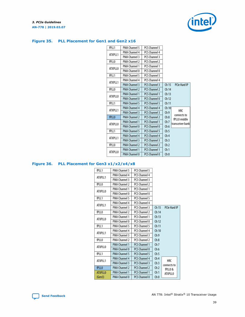
Figure 35. PLL Placement for Gen1 and Gen2 x16
PMA Channel 5PMA Channel 4PMA Channel 3PMA Channel 2PMA Channel 1PMA Channel 0
PCS Channel 5PCS Channel 4PCS Channel 3PCS Channel 2PCS Channel 1PCS Channel 0
fPLL1
fPLL0
ATXPLL0
ATXPLL1
PMA Channel 5PMA Channel 4PMA Channel 3PMA Channel 2PMA Channel 1PMA Channel 0
PCS Channel 5PCS Channel 4PCS Channel 3PCS Channel 2PCS Channel 1PCS Channel 0
fPLL1
fPLL0
ATXPLL0
ATXPLL1
PMA Channel 5PMA Channel 4PMA Channel 3PMA Channel 2PMA Channel 1PMA Channel 0
PCS Channel 5PCS Channel 4PCS Channel 3PCS Channel 2PCS Channel 1PCS Channel 0
fPLL1
fPLL0
ATXPLL0
ATXPLL1
PMA Channel 5PMA Channel 4PMA Channel 3PMA Channel 2PMA Channel 1PMA Channel 0
PCS Channel 5PCS Channel 4PCS Channel 3PCS Channel 2PCS Channel 1PCS Channel 0
fPLL1
fPLL0
ATXPLL0
ATXPLL1
Ch 15Ch 14Ch 13Ch 12Ch 11Ch 10Ch 9Ch 8Ch 7Ch 6Ch 5Ch 4Ch 3Ch 2Ch 1Ch 0
PCIe Hard IP
HRCconnects to
fPLL0 middletransceiver bank
Figure 36. PLL Placement for Gen3 x1/x2/x4/x8
PMA Channel 5PMA Channel 4PMA Channel 3PMA Channel 2PMA Channel 1PMA Channel 0
PCS Channel 5PCS Channel 4PCS Channel 3PCS Channel 2PCS Channel 1PCS Channel 0
fPLL1
fPLL0
ATXPLL0
ATXPLL1
PMA Channel 5PMA Channel 4PMA Channel 3PMA Channel 2PMA Channel 1PMA Channel 0
PCS Channel 5PCS Channel 4PCS Channel 3PCS Channel 2PCS Channel 1PCS Channel 0
fPLL1
fPLL0
ATXPLL0
ATXPLL1
PMA Channel 5PMA Channel 4PMA Channel 3PMA Channel 2PMA Channel 1PMA Channel 0
PCS Channel 5PCS Channel 4PCS Channel 3PCS Channel 2PCS Channel 1PCS Channel 0
fPLL1
fPLL0ATXPLL0(Gen3)
ATXPLL1
PMA Channel 5PMA Channel 4PMA Channel 3PMA Channel 2PMA Channel 1PMA Channel 0
PCS Channel 5PCS Channel 4PCS Channel 3PCS Channel 2PCS Channel 1PCS Channel 0
fPLL1
fPLL0
ATXPLL0
ATXPLL1
Ch 15Ch 14Ch 13Ch 12Ch 11Ch 10Ch 9Ch 8Ch 7Ch 6Ch 5Ch 4Ch 3Ch 2Ch 1Ch 0
PCIe Hard IP
HRCconnects to
fPLL0 &ATXPLL0
3. PCIe Guidelines
AN-778 | 2019.03.07
Send Feedback AN 778: Intel® Stratix® 10 Transceiver Usage
39
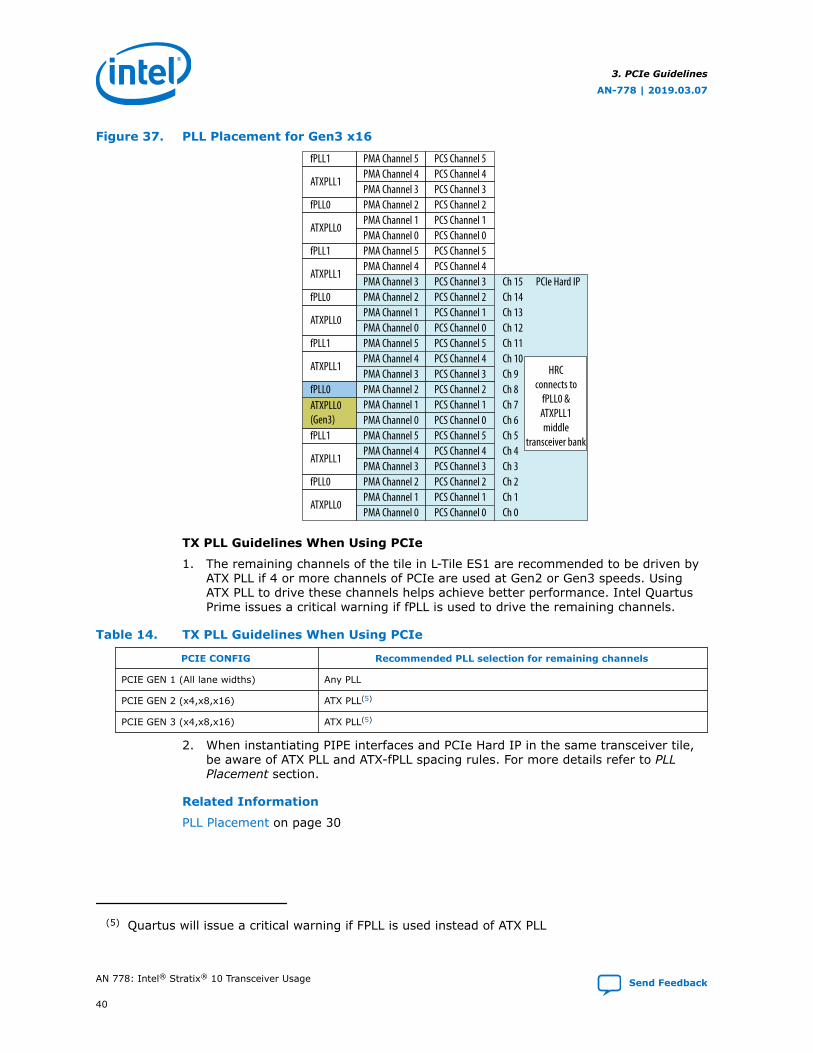
Figure 37. PLL Placement for Gen3 x16
PMA Channel 5PMA Channel 4PMA Channel 3PMA Channel 2PMA Channel 1PMA Channel 0
PCS Channel 5PCS Channel 4PCS Channel 3PCS Channel 2PCS Channel 1PCS Channel 0
fPLL1
fPLL0
ATXPLL0
ATXPLL1
PMA Channel 5PMA Channel 4PMA Channel 3PMA Channel 2PMA Channel 1PMA Channel 0
PCS Channel 5PCS Channel 4PCS Channel 3PCS Channel 2PCS Channel 1PCS Channel 0
fPLL1
fPLL0
ATXPLL0
ATXPLL1
PMA Channel 5PMA Channel 4PMA Channel 3PMA Channel 2PMA Channel 1PMA Channel 0
PCS Channel 5PCS Channel 4PCS Channel 3PCS Channel 2PCS Channel 1PCS Channel 0
fPLL1
fPLL0ATXPLL0(Gen3)
ATXPLL1
PMA Channel 5PMA Channel 4PMA Channel 3PMA Channel 2PMA Channel 1PMA Channel 0
PCS Channel 5PCS Channel 4PCS Channel 3PCS Channel 2PCS Channel 1PCS Channel 0
fPLL1
fPLL0
ATXPLL0
ATXPLL1
Ch 15Ch 14Ch 13Ch 12Ch 11Ch 10Ch 9Ch 8Ch 7Ch 6Ch 5Ch 4Ch 3Ch 2Ch 1Ch 0
PCIe Hard IP
HRCconnects to
fPLL0 &ATXPLL1middle
transceiver bank
TX PLL Guidelines When Using PCIe
1. The remaining channels of the tile in L-Tile ES1 are recommended to be driven byATX PLL if 4 or more channels of PCIe are used at Gen2 or Gen3 speeds. UsingATX PLL to drive these channels helps achieve better performance. Intel QuartusPrime issues a critical warning if fPLL is used to drive the remaining channels.
Table 14. TX PLL Guidelines When Using PCIe
PCIE CONFIG Recommended PLL selection for remaining channels
PCIE GEN 1 (All lane widths) Any PLL
PCIE GEN 2 (x4,x8,x16) ATX PLL(5)
PCIE GEN 3 (x4,x8,x16) ATX PLL(5)
2. When instantiating PIPE interfaces and PCIe Hard IP in the same transceiver tile,be aware of ATX PLL and ATX-fPLL spacing rules. For more details refer to PLLPlacement section.
Related Information
PLL Placement on page 30
(5) Quartus will issue a critical warning if FPLL is used instead of ATX PLL
3. PCIe Guidelines
AN-778 | 2019.03.07
AN 778: Intel® Stratix® 10 Transceiver Usage Send Feedback
40
3.2. PHY Interface for PCIe Express (PIPE)
This can be used when you want flexible channel placement or to interface the IntelStratix 10 PCIe PHY with existing 3rd party PCIe IP cores.
3.2.1. Channel Placement for PIPE
For L-Tile ES1 and L-Tile Production (PIPE only), any transceiver channel running atdata rate above 6.5 Gbps that shares a tile with an active PCI Express interface thatare Gen2 or Gen3 capable and configured with more than 2 lanes (Gen2/3 x4, x8,x16) may observe momentary bit errors (BER) during a PCI Express rate change event(PCIe link training both up and down, i.e., link down and start of link training ).Transceiver channels that share a tile with active PCI Express interfaces that are onlyGen1 capable are not impacted.
This is applicable for L-Tile ES1 and L-Tile Production (PIPE only).
For details on channel placement for PIPE, refer to the section "How to place channelsfor PIPE configurations" in" Intel Stratix 10 Transceiver PHY User Guide"
Related Information
How to Place Channels for PIPE Configurations
3.2.2. PLL Placement for PIPE
When instantiating PIPE interfaces and PCIe Hard IP in the same transceiver tile, beaware of ATX PLL and ATX-fPLL spacing rules. For more details refer to PLL Placementsection.
TX PLL Guidelines When Using PCIe
1. Intel recommends that the remaining channels of the tile in L-Tile ES1/L-TileProduction (PIPE only) are to be driven by ATX PLL if 4 or more channels of PCIeare used at Gen2 or Gen3 speeds. Using ATX PLL to drive these channels helpsachieve better performance. Intel Quartus Prime issues a critical warning if fPLL isused to drive the remaining channels.
Table 15. TX PLL Guidelines When Using PCIe
PCIE CONFIG Recommended PLL selection for remaining channels
PCIE GEN 1 (All lane widths) Any PLL
PCIE GEN 2 (x4,x8,x16) ATX PLL(6)
PCIE GEN 3 (x4,x8,x16) ATX PLL(6)
2. For details on PLL placement for PIPE, refer to the section "How to Connect TXPLLs for PIPE Gen1, Gen2, and Gen3 Modes" in" Intel Stratix 10 Transceiver PHYUser Guide"
Related Information
• PLL Placement on page 30
• How to Connect TX PLLs for PIPE Gen1, Gen2, and Gen3 Modes
(6) Quartus issues a critical warning if FPLL is used instead of ATX PLL
3. PCIe Guidelines
AN-778 | 2019.03.07
Send Feedback AN 778: Intel® Stratix® 10 Transceiver Usage
41

4. Document Revision History for AN 778: Intel Stratix 10Transceiver Usage
DocumentVersion
Changes
2019.03.07 Made the following change:• Changed the data rate for E-tile Non-Return to Zero (NRZ) to 28.9 Gbps.
2018.07.13 Made the following changes:• Updated the "ATX PLL Block Diagram" figure to clearly show that cascaded input from an upstream
PLL is not supported.• Added "These combinations are only applicable for banks GXB1D/H/L and GXB4D/H/L and
GXB1F/J/N and GXB4F/J/N." note to Possible Combinations of GX and GXT Channels in L-TileProduction.
2017.11.06 Made the following changes:• Added a new diagram "Intel Stratix 10 L-Tile ES2 Production GXT Channel Placement"• Updated the "Channel Types" table to include L-Tile channels• Updated the "ATX PLL Spacing Requirements" and "ATX PLL-fPLL Spacing Requirements" table• Updated the "Thermal Guidelines" section• Made the following updates in the "Mix and Match GX Channels Design Example" diagram:
— Changed PCIe Gen 1/2/3 x8 to PCIe HIP Gen 1/2/3x8— Changed PCIe Gen 1/2 , 2.5 GHz to PCIe HIP Gen 1/2 , 2.5 GHz— Changed PCIe Gen 3, 4 GHz to PCIe HIP Gen 3, 4 GHz
• Updated the description for "TX PLL Restrictions when Using PCIe x16" topic• Updated the description for "PCIe Hard IP Placement" topic• Restrictions stated when one or more channels in a bank are used for PCIe/PIPE Gen3• Updated steps in "How to Place Channels for PIPE Configurations" topic• Changed value of Logical PCS Master Channel # from 1 to 0 in "Logical PCS Master Channel for PIPE
Configuration" table• Added a note "Each core clock network reference clock pin cannot drive fPLLs located on multiple
L/H-Tiles"• Added a new diagram "x4 Configuration" in "Bonded GX Channels" topic to explain the ascending
order of the channel placement
2017.01.13 Made the following change:• Added a new section: ATX PLL GXT Channels Placement
2016.12.19 Made the following changes:• Clarified the ATX PLL spacing requirements and listed them in the "ATX PLL Spacing Requirements"
table.
2016.09.20 Initial release
AN-778 | 2019.03.07
Send Feedback
Intel Corporation. All rights reserved. Intel, the Intel logo, Altera, Arria, Cyclone, Enpirion, MAX, Nios, Quartusand Stratix words and logos are trademarks of Intel Corporation or its subsidiaries in the U.S. and/or othercountries. Intel warrants performance of its FPGA and semiconductor products to current specifications inaccordance with Intel's standard warranty, but reserves the right to make changes to any products and servicesat any time without notice. Intel assumes no responsibility or liability arising out of the application or use of anyinformation, product, or service described herein except as expressly agreed to in writing by Intel. Intelcustomers are advised to obtain the latest version of device specifications before relying on any publishedinformation and before placing orders for products or services.*Other names and brands may be claimed as the property of others.
ISO9001:2015Registered


