
Aspects of Dirac Physics in Graphene
K. Sengupta
Indian Association for the Cultivation of Sciences, Kolkata
Overview
1. Origin of Dirac physics in graphene
2. Superconducting junctions
3. Physics of graphene junctions
4. Kondo physics and STM spectroscopy in graphene
5. Conclusion
Origin of Dirac physics in graphene
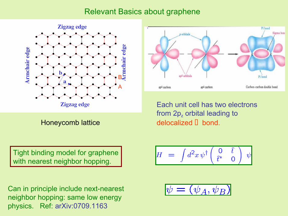
Relevant Basics about graphene
A
B
Tight binding model for graphenewith nearest neighbor hopping.
Can in principle include next-nearest neighbor hopping: same low energyphysics. Ref: arXiv:0709.1163
Each unit cell has two electronsfrom 2pz orbital leading to delocalized bond.Honeycomb lattice
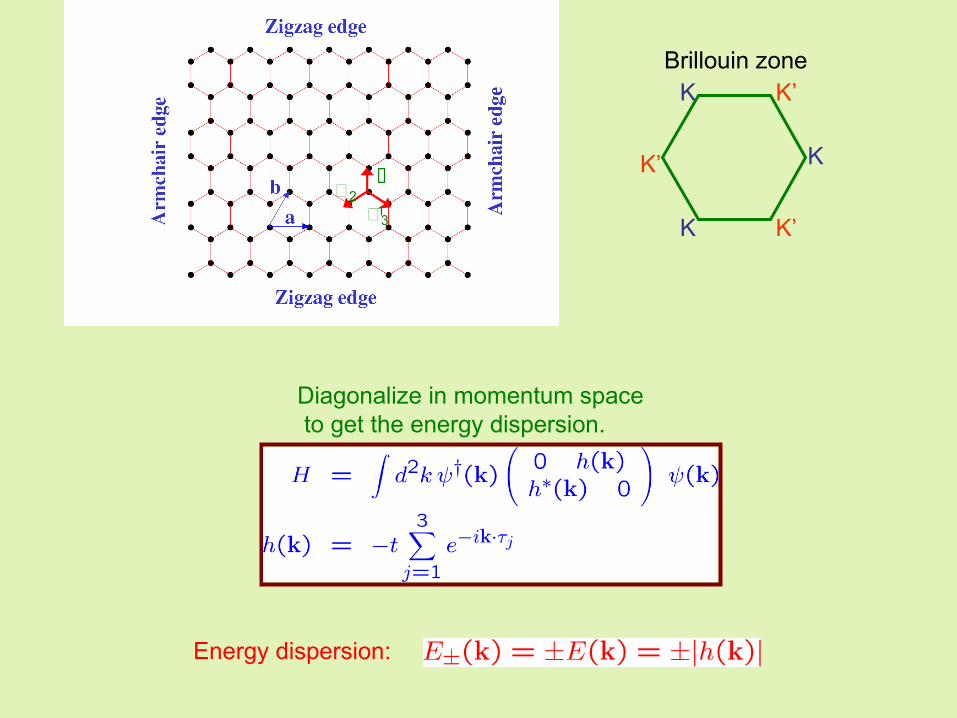
Diagonalize in momentum space to get the energy dispersion.
12
3
Brillouin zoneK’
K’
K’
K
K
K
Energy dispersion:

There are two energy bands (valence and conduction)corresponding to energies
Two inequivalent Fermi points rather than a Fermi-line.
These two bands touch each otherat six points at the edges of the Brillouin zone
Two of these points K and K’are inequivalent; rest are related by translation of a lattice vector.
Dirac cone about the K and K’ points
No large k scattering leads to two species of massless Dirac Fermions.
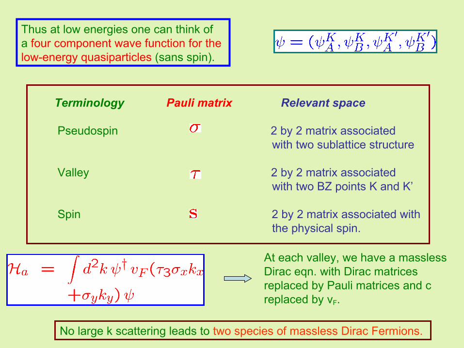
Thus at low energies one can think of a four component wave function for the low-energy quasiparticles (sans spin).
Terminology Pauli matrix Relevant space
Pseudospin 2 by 2 matrix associated with two sublattice structure
Valley 2 by 2 matrix associated with two BZ points K and K’
Spin 2 by 2 matrix associated with the physical spin.
At each valley, we have a masslessDirac eqn. with Dirac matrices replaced by Pauli matrices and c replaced by vF.
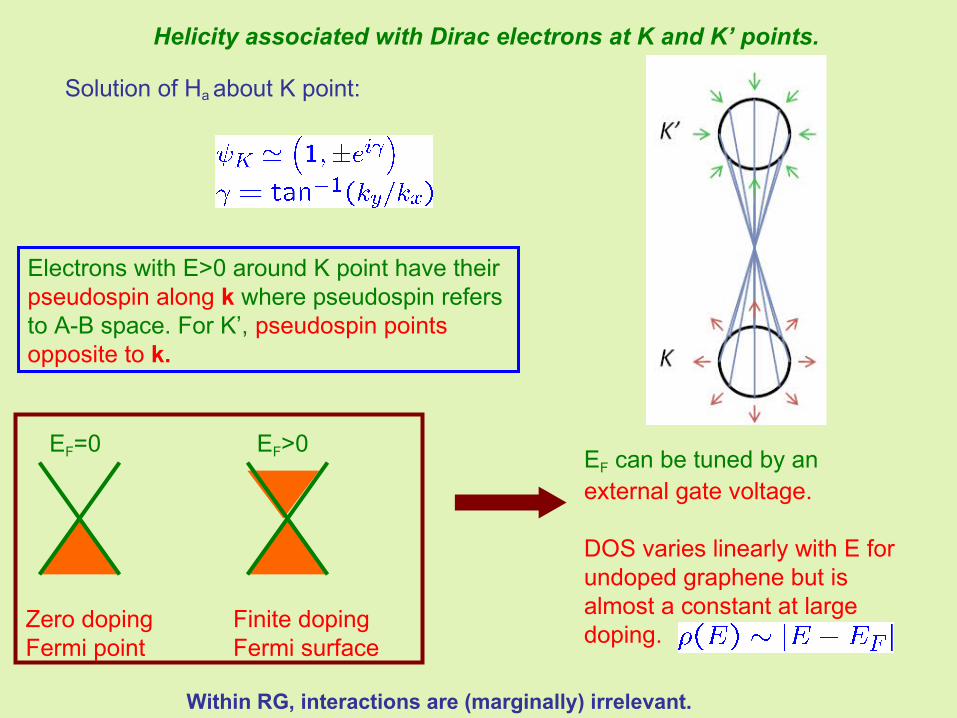
Zero dopingFermi point
Finite dopingFermi surface
EF can be tuned by an external gate voltage.
DOS varies linearly with E forundoped graphene but is almost a constant at large doping.
EF=0 EF>0
Helicity associated with Dirac electrons at K and K’ points.
Electrons with E>0 around K point have theirpseudospin along k where pseudospin refers to A-B space. For K’, pseudospin points opposite to k.
Solution of Ha about K point:
Within RG, interactions are (marginally) irrelevant.
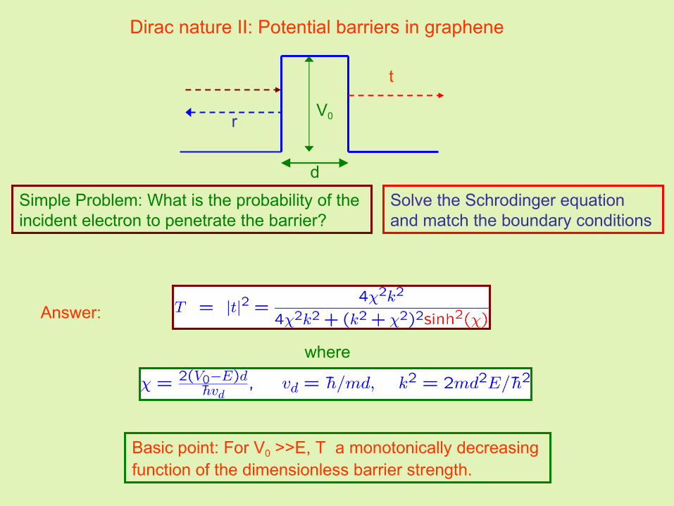
Dirac nature II: Potential barriers in graphene
V0
t
r
d
Simple Problem: What is the probability of the incident electron to penetrate the barrier?
Solve the Schrodinger equationand match the boundary conditions
Answer:
where
Basic point: For V0 >>E, T a monotonically decreasing function of the dimensionless barrier strength.
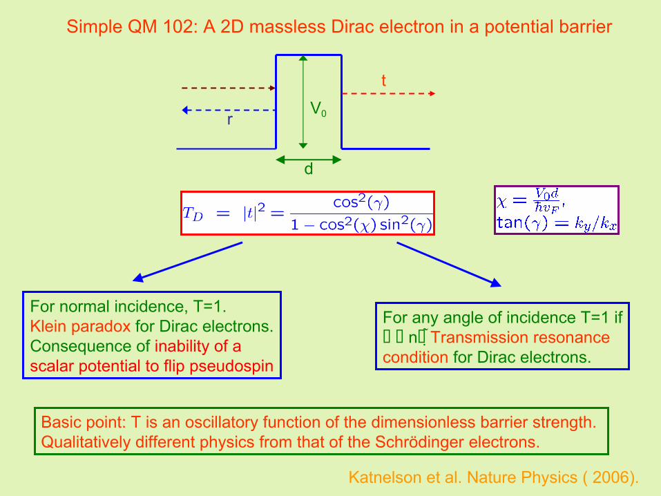
Simple QM 102: A 2D massless Dirac electron in a potential barrier
V0
t
r
d
Basic point: T is an oscillatory function of the dimensionless barrier strength. Qualitatively different physics from that of the Schrödinger electrons.
For normal incidence, T=1.Klein paradox for Dirac electrons.Consequence of inability of a scalar potential to flip pseudospin
For any angle of incidence T=1 if n Transmission resonance condition for Dirac electrons.
Katnelson et al. Nature Physics ( 2006).

Conventional Superconducting junctions

Superconductivity and tunnel junctions
Measurement of tunneling conductance
eV
Normal metal (N) Superconductor (S)
Insulator (I)
eV
Normal metal (N)
Insulator (I)
Normal metal (N)
N-I-N interface
N-I-S interface

N I S
Andreev reflection2e charge transfer
Basic mechanism of current flow in a N-I-S junction
Andreev reflection is strongly suppressed in conventional junctions if the insulating layer provides a large potential barrier: so called tunneling limit
In conventional junctions, subgap tunneling conductance is a monotonically decreasing function of the effective barrier strength Z.
BTK, PRB, 25 4515 (1982)
Zero bias tunneling condutancedecays as 1/(1+2z^2)^2 with increasing barrier strength.
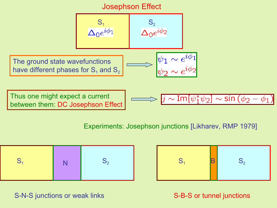
Josephson Effect
S1 S2
The ground state wavefunctionshave different phases for S1 and S2
Thus one might expect a current between them: DC Josephson Effect
Experiments: Josephson junctions [Likharev, RMP 1979]
S1 S2N
S-N-S junctions or weak links
S1 S2B
S-B-S or tunnel junctions
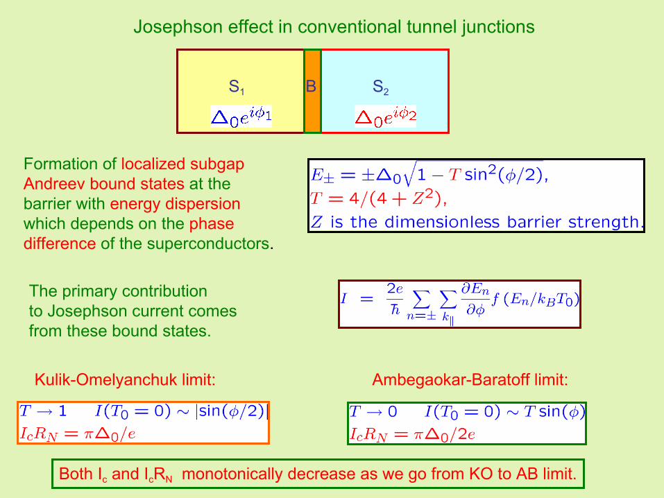
Josephson effect in conventional tunnel junctions
S1 S2B
Formation of localized subgap Andreev bound states at the barrier with energy dispersionwhich depends on the phasedifference of the superconductors.
The primary contributionto Josephson current comesfrom these bound states.
Kulik-Omelyanchuk limit: Ambegaokar-Baratoff limit:
Both Ic and IcRN monotonically decrease as we go from KO to AB limit.
Graphene Junctions
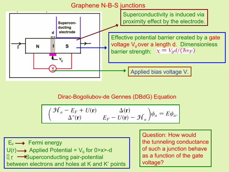
Graphene N-B-S junctionsSuperconductivity is induced viaproximity effect by the electrode.
Effective potential barrier created by a gate voltage Vg over a length d. Dimensionless barrier strength:
Dirac-Bogoliubov-de Gennes (DBdG) Equation
EF Fermi energyU(r) Applied Potential = Vg for 0>x>-d
r Superconducting pair-potential between electrons and holes at K and K’ points
Question: How wouldthe tunneling conductanceof such a junction behave as a function of the gate voltage?
Applied bias voltage V.

Results in the thin barrier limit
Central Result: In complete contrast to conventional NBS junction,Graphene NBS junctions, due to the presence of Dirac-like dispersion of its electrons, exhibit novel periodic oscillatory behavior of subgap tunneling conductance as the barrier strength is varied.
periodic oscillations of subgaptunneling conductance as a function of barrier strength
Tunneling conductance maximaoccur at =(n+1/2)
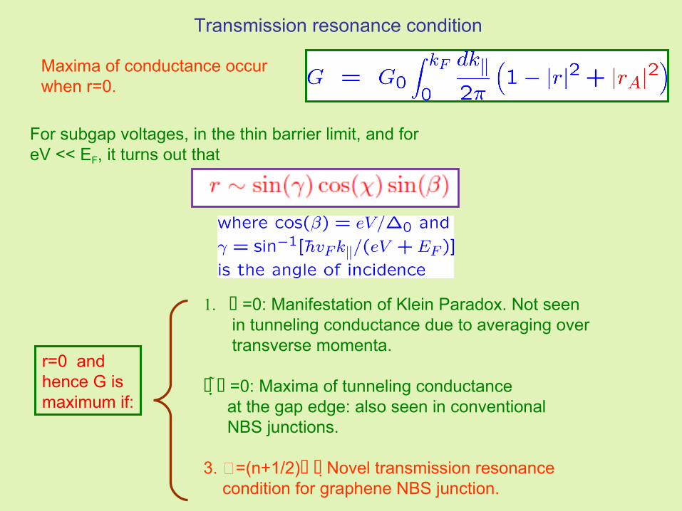
Transmission resonance condition
Maxima of conductance occurwhen r=0.
For subgap voltages, in the thin barrier limit, and foreV << EF, it turns out that
r=0 and hence G is maximum if:
.1 =0: Manifestation of Klein Paradox. Not seen in tunneling conductance due to averaging over transverse momenta.
=0: Maxima of tunneling conductance at the gap edge: also seen in conventional NBS junctions.
3. =(n+1/2) Novel transmission resonance condition for graphene NBS junction.

Oscillations persists: so one expects the oscillatory behavior both as functions of VG and d to be robust.
However, the maximum value of Gmay be lesser than the Andreev limit value of 2G0
The periodicity of the oscillations shall vary with VG and will deviate from
0.2
0.4
0.6
0.8
1
dミl 10
15
20
V0ミEF
1
1.2
1.4
1.6
1.8
GミG0
0.2
0.4
0.6
0.8
1
dミl
Not so thin barrier
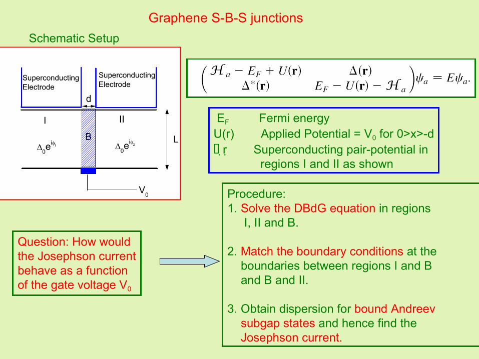
Graphene S-B-S junctions
EF Fermi energyU(r) Applied Potential = V0 for 0>x>-d
r Superconducting pair-potential in regions I and II as shown
Question: How would the Josephson currentbehave as a functionof the gate voltage V0
Procedure:1. Solve the DBdG equation in regions I, II and B.
2. Match the boundary conditions at the boundaries between regions I and B and B and II.
3. Obtain dispersion for bound Andreev subgap states and hence find the Josephson current.
Schematic Setup
0
2
4
6
f
0
2
4
6
8
c
00.250.5
0.751
e+タタタタタタタタタD0
0
2
4
6
f
0
2
4
6
f
0
2
4
6
8
c
- 4
- 2
0
2
4
IタタタタタタタI0
0
2
4
6
f
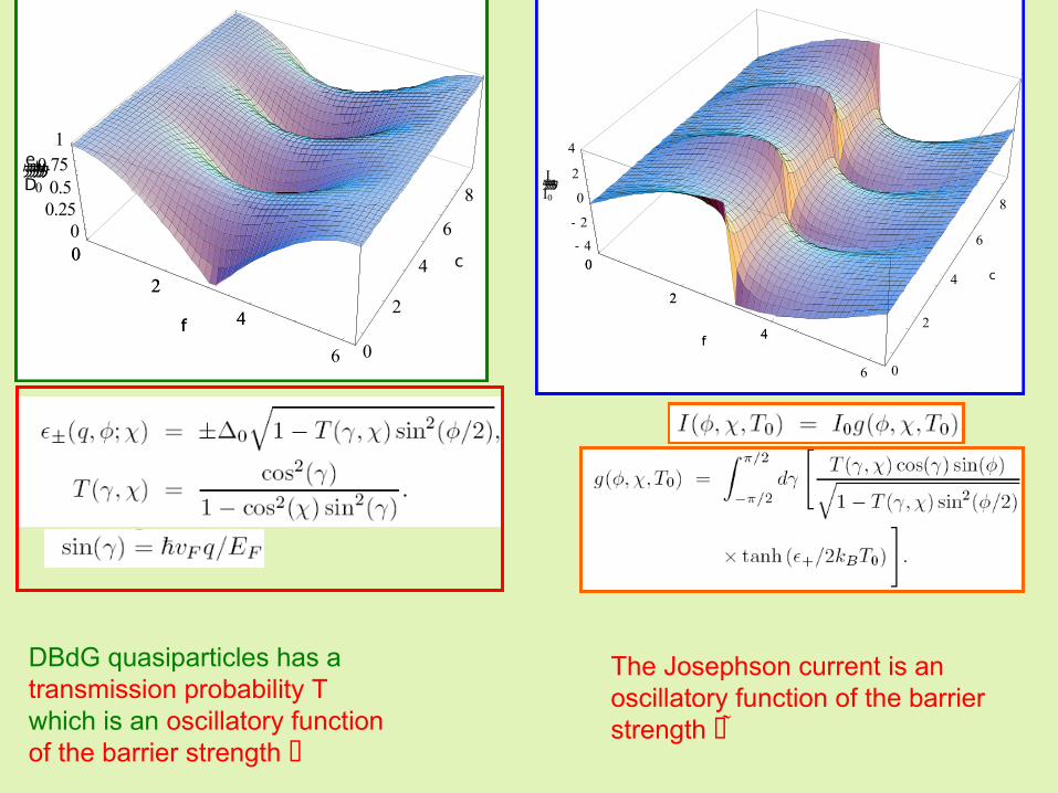
DBdG quasiparticles has atransmission probability Twhich is an oscillatory functionof the barrier strength
The Josephson current is an oscillatory function of the barrierstrength
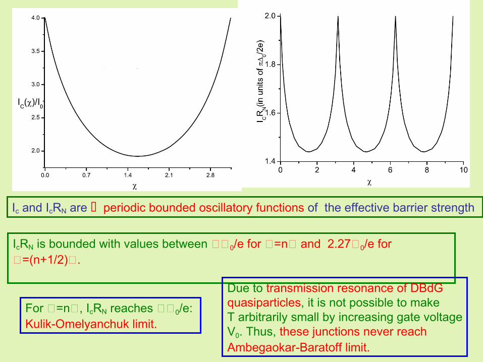
Ic and IcRN are periodic bounded oscillatory functions of the effective barrier strength
For =n, IcRN reaches 0/e: Kulik-Omelyanchuk limit.
IcRN is bounded with values between 0/e for =n and 2.270/e for =(n+1/2).
Due to transmission resonance of DBdGquasiparticles, it is not possible to makeT arbitrarily small by increasing gate voltageV0. Thus, these junctions never reach Ambegaokar-Baratoff limit.

Kondo Physics and STM spectroscopy
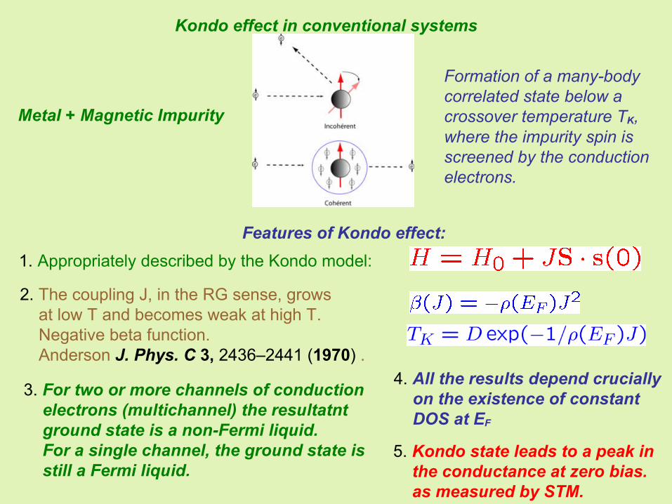
Kondo effect in conventional systems
Formation of a many-body correlated state below a crossover temperature TK, where the impurity spin is screened by the conduction electrons.
Metal + Magnetic Impurity
Features of Kondo effect:
1. Appropriately described by the Kondo model:
2. The coupling J, in the RG sense, grows at low T and becomes weak at high T. Negative beta function. Anderson J. Phys. C 3, 2436–2441 (1970) .
3. For two or more channels of conduction electrons (multichannel) the resultatnt ground state is a non-Fermi liquid. For a single channel, the ground state is still a Fermi liquid.
4. All the results depend crucially on the existence of constant DOS at EF
5. Kondo state leads to a peak in the conductance at zero bias. as measured by STM.

What’s different for possible Kondo effect in graphene
Theoretical prediction: Sengupta and Baskaran PRB (2007)
For undoped graphene, linearly varyingDOS makes a Kondo screened phase impossible [Casselano and Fradkin, Ingersent, Polkovnikov, Sachdev and Vojta].
At finite and large doping, aneffectively constant DOS occursand hence one should see a Kondo screened phase.
One can tune into a Kondo screened phase by applying a gate voltage
Also, two species of electrons from Kand K’ points may act as two channelsif the impurity radius is large enough sothat large-momenta scatterings are suppressed.
Possibility of two-channelKondo effect in graphene.
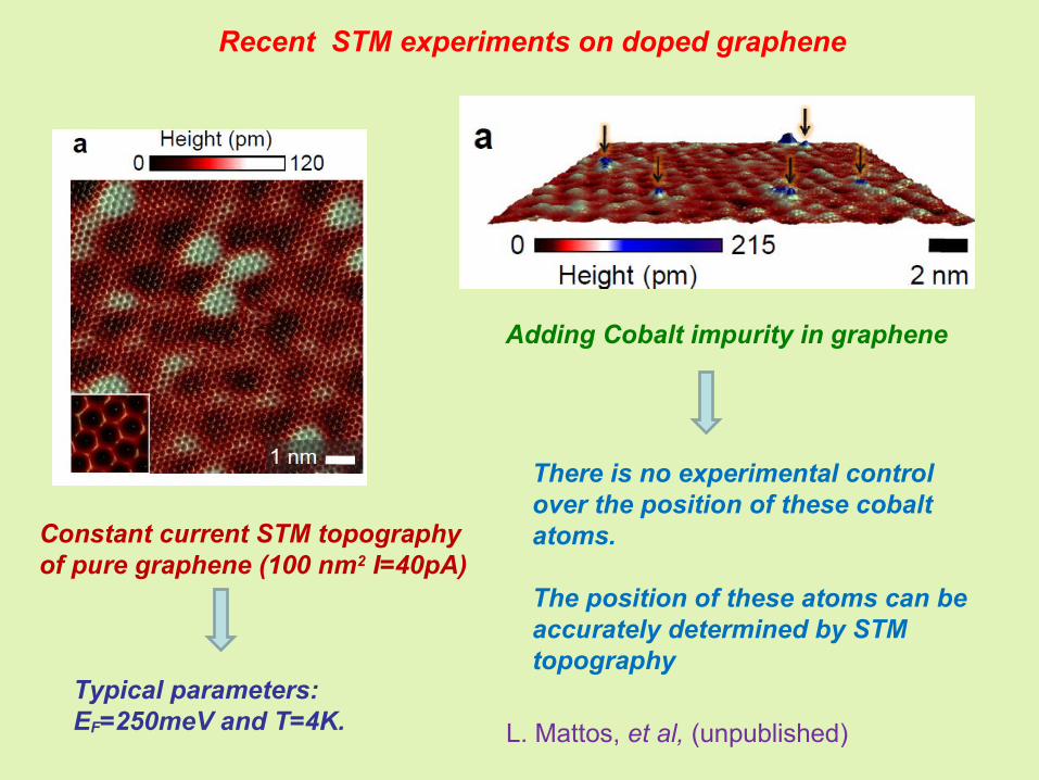
Recent STM experiments on doped graphene
Constant current STM topographyof pure graphene (100 nm2 I=40pA)
Adding Cobalt impurity in graphene
There is no experimental control over the position of these cobalt atoms.
The position of these atoms can be accurately determined by STM topography
Typical parameters: EF=250meV and T=4K. L. Mattos, et al, (unpublished)
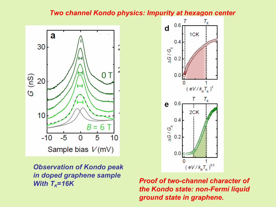
Observation of Kondo peakin doped graphene sampleWith TK=16K Proof of two-channel character of
the Kondo state: non-Fermi liquid ground state in graphene.
Two channel Kondo physics: Impurity at hexagon center
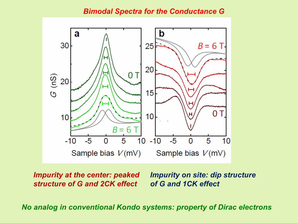
Bimodal Spectra for the Conductance G
No analog in conventional Kondo systems: property of Dirac electrons
Impurity at the center: peakedstructure of G and 2CK effect
Impurity on site: dip structure of G and 1CK effect
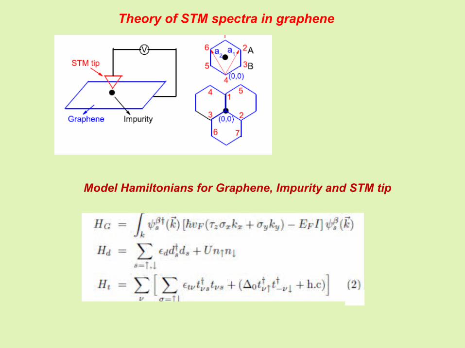
Theory of STM spectra in graphene
Model Hamiltonians for Graphene, Impurity and STM tip
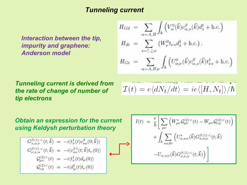
Tunneling current
Interaction between the tip,impurity and graphene:Anderson model
Tunneling current is derived fromthe rate of change of number of tip electrons
Obtain an expression for the current using Keldysh perturbation theory
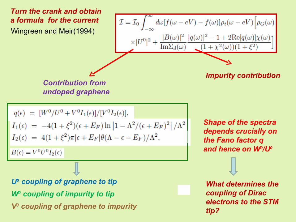
Turn the crank and obtain a formula for the current
Wingreen and Meir(1994)
Contribution from undoped graphene
Impurity contribution
Shape of the spectradepends crucially on the Fano factor qand hence on W0/U0
U0 coupling of graphene to tip
W0 coupling of impurity to tip
V0 coupling of graphene to impurity
What determines the coupling of Dirac electrons to the STM tip?
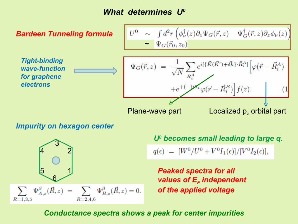
What determines U0
Bardeen Tunneling formula~
Tight-bindingwave-functionfor graphene electrons
Plane-wave part Localized pz orbital part
Impurity on hexagon center
U0 becomes small leading to large q.
1
3
5
4 2
6Peaked spectra for allvalues of EF independentof the applied voltage
Conductance spectra shows a peak for center impurities
1
3
2
4
6
5
7
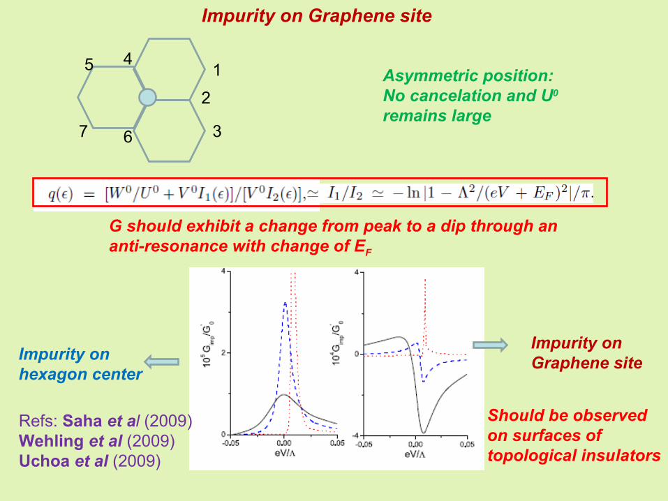
Asymmetric position: No cancelation and U0
remains large
Impurity on Graphene site
G should exhibit a change from peak to a dip through an anti-resonance with change of EF
Impurity on Graphene siteImpurity on
hexagon center
Should be observed on surfaces of topological insulators
Refs: Saha et al (2009)Wehling et al (2009)Uchoa et al (2009)

Conclusion
1. The field of graphene has shown unprecedented progress over the last few years. First example of so called “ Dirac materials”.
2. Several interesting physics phenomenon: a) Dirac physics on a tabletop. b) Unconventional Kondo physics c) STM spectroscopy with Dirac fermions.
3. Potential applications in engineering:
a) Detection of gas molecules with great precision b) Possibility of nanoscale room temperature transistors.
4. Future:
a) Controlled sample preparation and better lithography. b) More strongly correlated phenomenon such as FQHE. c) Graphene based electronics: future direction of nanotechnology?


