

CMPE 650 – High Speed Digital Design
Final Project
Audio Acquisition, Storage and Playback
Jerome Stanislaus
Kirit Chatterjee
Spring 2011
Introduction:
The goal of this project is to design a PCB to capture audio signal through a
playback from the card through a speaker
and analyzing using MATLAB.
The project had a problem that the input from the microphone picked up a lot
going to the ADC. Also, the 2 LSBs of the ADC are stuck at 01 and hence
from these, the other parts of the project worked fine as expected. The audio capturing is tested by pr
low frequency SINE and TRIANGULAR at the input of the ADC and stored it to the SD Card. The
using DAC and SD Card are tested using a WAV file present inside the SD card
Materials Used:
IC PIN Package
TPA6111A2 8 SOIC
TLC7524 16 SOIC
OPA344 8 SOIC
TLC0820A 20 SOIC
ATMEGA328P 28 DIP/SMD
LD1117S33CTR 4 SOT-223
Table 1. List of ICs used and their function
Block Diagram & Theory:
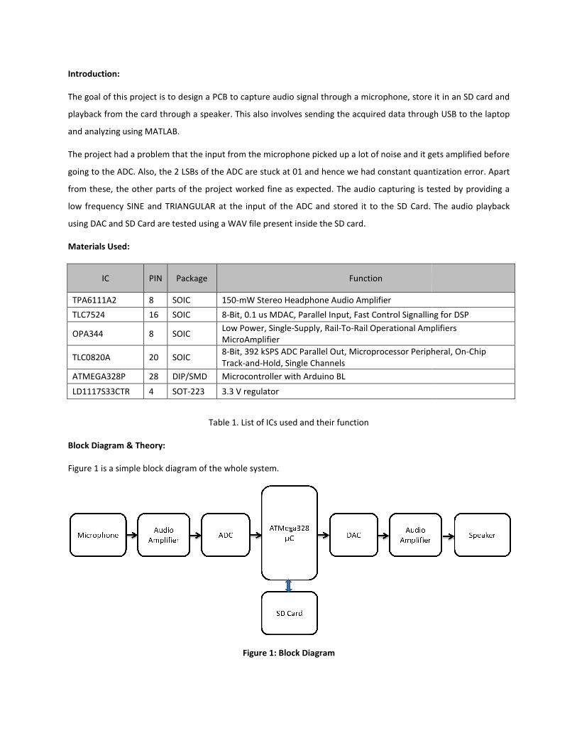
Figure 1 is a simple block diagram of the whole system.
The goal of this project is to design a PCB to capture audio signal through a microphone, store it in an SD card and
playback from the card through a speaker. This also involves sending the acquired data through USB to the laptop
The project had a problem that the input from the microphone picked up a lot of noise and it gets amplified before
going to the ADC. Also, the 2 LSBs of the ADC are stuck at 01 and hence we had constant quantization error. Apart
other parts of the project worked fine as expected. The audio capturing is tested by pr
low frequency SINE and TRIANGULAR at the input of the ADC and stored it to the SD Card. The
DAC and SD Card are tested using a WAV file present inside the SD card.
Function
150-mW Stereo Headphone Audio Amplifier
8-Bit, 0.1 us MDAC, Parallel Input, Fast Control Signalling fo
Low Power, Single-Supply, Rail-To-Rail Operational Amplifiers
MicroAmplifier
8-Bit, 392 kSPS ADC Parallel Out, Microprocessor Peripheral, On
Track-and-Hold, Single Channels
Microcontroller with Arduino BL
3.3 V regulator
Table 1. List of ICs used and their function
Figure 1 is a simple block diagram of the whole system.
Figure 1: Block Diagram
microphone, store it in an SD card and
the acquired data through USB to the laptop
of noise and it gets amplified before
quantization error. Apart
other parts of the project worked fine as expected. The audio capturing is tested by providing a
low frequency SINE and TRIANGULAR at the input of the ADC and stored it to the SD Card. The audio playback
Bit, 0.1 us MDAC, Parallel Input, Fast Control Signalling for DSP
Rail Operational Amplifiers
Bit, 392 kSPS ADC Parallel Out, Microprocessor Peripheral, On-Chip
The microphone picks up audio signal and is amplified by the audio amplifier. The output of the audio amplifier is
converted to digital data by an 8-bit ADC and sent to the microcontroller. The microcontroller stores it into the SD
card in WAV format. After this, the ADC circuit is switched off and the microcontroller retrieves the stored data
from the SD card and sends it to the DAC. Here, the digital data is converted back to analog signal which is then
amplified and is played back through the speaker. The microcontroller is the master control of the circuit and is
responsible for switching on and off each part of the system while working.
The data is captured at a sample rate of 25 KHz. The audio signals range from 20 Hz to 20 KHz and human voice
frequency ranges from 300 Hz to 3.4 KHz. Hence the sampling rate of 25 KHz is a good choice. Since the data sent
to the SD card is serial, the data transfer rate is greater than 200 KHz. Hence from this data, it can be calculated
that the delay required per sample is 1/25000 = 40 µs.
Procedure Followed:
• First, a decision regarding which project to choose was taken. This project was chosen because it seemed
to a feasible choice considering the time frame that we were supposed to do it in.
• Then the circuits were designed and implemented using the Cadence Design Entry CIS tool. The design
spanned 4 pages, each covering a part of the project.
• After the circuits were successfully designed, we designed a 2 layer board using the Allegro PCB Editor
tool. We wanted to see whether we could successfully implement it on a 2 layer board instead of a 4 layer
one. All the routing was done manually.
• The board was fabricated “in-house”, drilled and soldered.
• Testing of the board took time comparable to the design of the same. For testing, we followed these
steps:
Test microcontroller
Test SD card.
Test DAC conversion and play audio file from SD card.
Test ADC conversion
Play sound into microphone and test the whole system.
Circuits & Discussion:
1.Audio Capturing
The ADC circuit is shown in Figure 2.

Figure 2: Microphone-ADC Circuit
The connector on the left is where the microphone is plugged in and the high pass filter feeds it into the
operational amplifier. The amplified output is fed into the ADC and converted. The signal from the microphone
picked up a huge amount of noise that is being amplified and hence makes it improbable to expect the ADC to give
sensible conversions on the audio input. The LED (D3) is fixed just as an indicator to see if the circuit is switched on
or not. The output of the amplifier is fed to a speaker and found that it picked up so much of noise and still could
hear the audio with low gain.
The bits D0 to D7 (as seen on the right) are the data ports connected to the microcontroller along with the CS and
RDB signals. The ADC interface is “parallel” that makes things easier and the CS pin is for selecting the chip before
reading the data using RDB pin. The timing diagram for the ADC is given below.

Figure 3. Timing Diagram for ADC
The CS pin should be pulled low before reading any data from the ADC. After a delay of 1 µs, the RD pin is pulled
low. Now, after 1 µs the data will be ready to read and this data is taken by the microcontroller. Since the sampling
requires 40 µs delay, we have ample time for the above process. This is repeated every 40 µs and stored it in SD
card.
2. Microcontroller
Figure 4 here shows the microcontroller connections.

Figure 4. Microcontroller Circuit
The switch was implemented to facilitate the control (switching on/off) of the ADC and the DAC circuits separately.
The LEDs again are used as indicators here. The switch SW2 is a push button switch that is used to reset the
microcontroller whenever required. All the references are given to Vcc and Gnd as and when required. The bit
lines, D0 to D7, are connected to the ADC and DAC circuits. The control over the bits is handled with software.
CONN6 is for external connections like power supply, serial transmission to USB, etc.
The microcontroller has arduino bootloader and I programmed using Arduino ISP. The software for the
microcontroller is written using C (modified for arduino) and flashed using Arduino IDE. Arduino is an open source
and is available online.
The interface to the DAC and ADC are design by ourselves and the interface to the SD card is achieved by FAT File
system library found in the arduino forum [3]. The software contains 2 buffers of size 256 bytes. In case of audio
acquisition, the data is read from the port D0-D7 and stored in the buffer1. Once the buffer 1 is full, the controller
starts filling the buffer2. During this time, the contents of buffer 1 is written to the SD card. Once buffer2 is filled,
the data is filled in buffer1 and during this time, the data in buffer 2 is written to the SD card. This process is
continued till the audio acquisition is complete. The 25 KHz signal is generated using timer interrupt present in the

controller. The timer is set to interrupt once in every 40 µs to achieve the required interrupt. So every time the ISR
is called, the data is read from the ADC or written to the DAC depending upon the operation we are doing.
An addition to this circuit is Figure 4 which was made because the whole thing couldn’t fit on one Design Entry CIS
page.
3. SD Card Interface
Figure 5. SD Card Circuit
The figure here shows the SD card connections from the microcontroller. The 8-pin connector on the right is where
the SD card is inserted. The data is controlled as before by the microcontroller. The SD card runs in 3.3 V and hence
a voltage divider circuit is used for all the input/output lines to/from the SD card. The 4 lines to the SD card are
given as:
Pin Function
DI Serial Data In
SCK Serial Clock
DO Serial Data out
CS Chip Select
Table 2. Ports for SD Card
4 .Audio Playback
Figure 6 shows the DAC circuit.
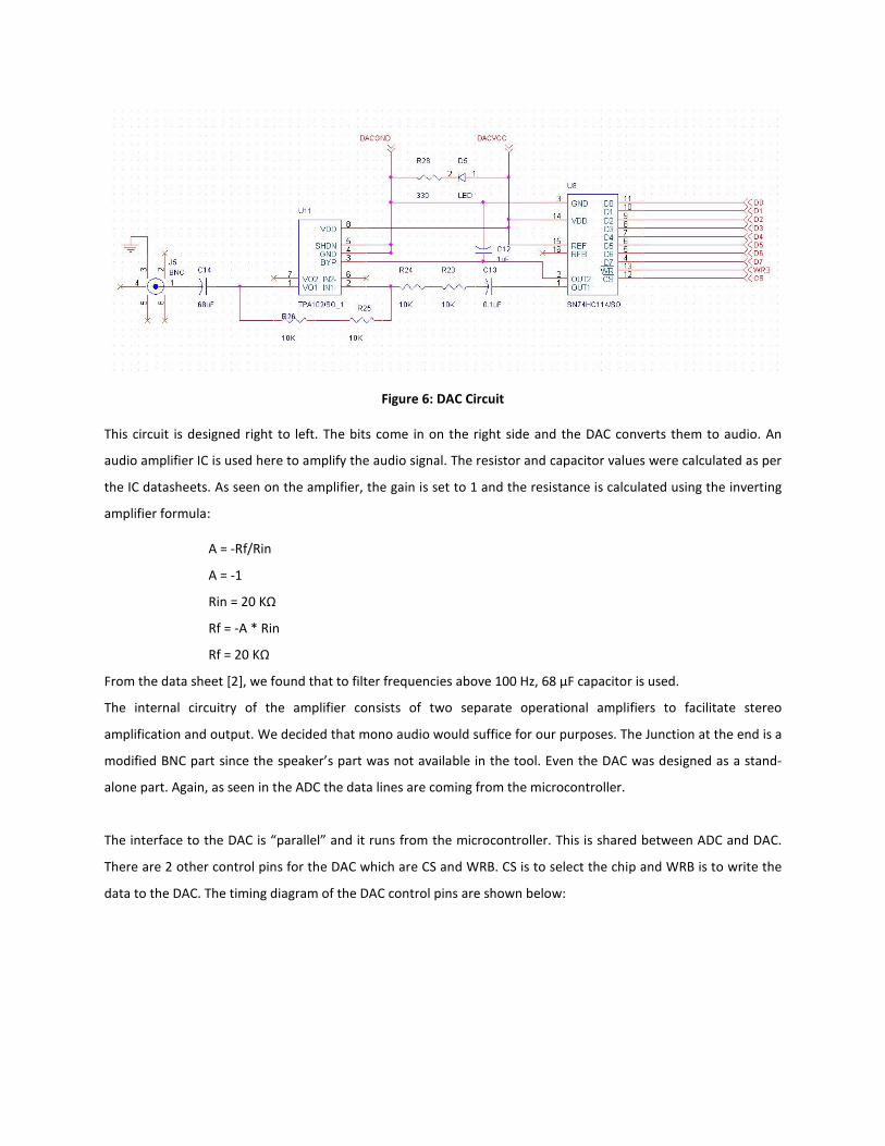
Figure 6: DAC Circuit
This circuit is designed right to left. The bits come in on the right side and the DAC converts them to audio. An
audio amplifier IC is used here to amplify the audio signal. The resistor and capacitor values were calculated as per
the IC datasheets. As seen on the amplifier, the gain is set to 1 and the resistance is calculated using the inverting
amplifier formula:
A = -Rf/Rin
A = -1
Rin = 20 KΩ
Rf = -A * Rin
Rf = 20 KΩ
From the data sheet [2], we found that to filter frequencies above 100 Hz, 68 µF capacitor is used.
The internal circuitry of the amplifier consists of two separate operational amplifiers to facilitate stereo
amplification and output. We decided that mono audio would suffice for our purposes. The Junction at the end is a
modified BNC part since the speaker’s part was not available in the tool. Even the DAC was designed as a stand-
alone part. Again, as seen in the ADC the data lines are coming from the microcontroller.
The interface to the DAC is “parallel” and it runs from the microcontroller. This is shared between ADC and DAC.
There are 2 other control pins for the DAC which are CS and WRB. CS is to select the chip and WRB is to write the
data to the DAC. The timing diagram of the DAC control pins are shown below:

Figure 7. Timing Diagram for DAC [2]
The CS pin should be pulled low before writing any data to the DAC. After a delay of 1 µs, the WRB pin is pulled
low. Now the DAC is ready to read the get the data from the controller. Once the data is placed in the pins, the
WRB is taken high. Now the DAC output is proportional to the input given. The after 1 µs delay the CS is taken high.
Since the sampling requires 40 µs delay, we have ample time for the above process. This is repeated every 40 µs
and stored it in SD card.
Working
So, overall the circuit works but there are a few problems. The microphone is picking up a lot of noise and thus the
ADC conversion is faulty. The microcontroller circuitry works perfectly and is able to manipulate the data. The DAC
circuitry works fine and converts audio to a near ideal output.
To test the ADC and the data capturing capability of the microcontroller, the input to the ADC is disconnected from
the audio input from the microphone. A sine or triangular wave of amplitude 1 V and an offset of 1 V is fed to the
ADC input. The frequency of the signal is set to 100 Hz to 1 KHz and tested. The microcontroller could read the
data from the ADC and store the data into SD card as explained before. The check the data from the SD card, the
data is sent serially to the COM port of the laptop and by using Matlab, the data is captured and plotted. The
captured signal is shown below:

Figure 8. Analog Data capturing with Triangular Input
When zoomed in, it is found that the LSB 2 bits are held constant at 01
trying to find the source of the issue, it is seen that the data read from the ADC is fine and it is also fine when seen
from the microcontroller. We suspect that the error may be due to the serial transmission thr
are not sure about the problem.
Figure 9. Zoomed In View of the above triangular input showing quantization error
Figure 8. Analog Data capturing with Triangular Input
When zoomed in, it is found that the LSB 2 bits are held constant at 01 and this gives a quantization error. When
trying to find the source of the issue, it is seen that the data read from the ADC is fine and it is also fine when seen
from the microcontroller. We suspect that the error may be due to the serial transmission through the USB and we
Figure 9. Zoomed In View of the above triangular input showing quantization error
and this gives a quantization error. When
trying to find the source of the issue, it is seen that the data read from the ADC is fine and it is also fine when seen
ough the USB and we
Figure 9. Zoomed In View of the above triangular input showing quantization error

Since we tried to multiplex the data lines to DAC and ADC using same pin and tried to disconnect the power source
of ADC/DAC while applying input to the IC, Dr. Robucci felt that the chip might have burnt. But so far the ICs are
working fine but for the 2 LSB bit errors. Later after the project demonstration, we found that there is no need to
disconnect the power source from any of the ICs and we can turn on/off the IC using CS pin fed to the ICs. So this
will fix the major problem in the board design and still satisfy the function of working.
Now to test the DAC and audio playback, we took a wave file of 25 KHz sampling rate and 8 bit resolution mono
audio and stored it in the SD card. Since the file system interface to the SD card is FAT, it was easy to store the data
into the SD card using a laptop and read it using the microcontroller. The song is then played back as explained
before and the song is listened using the earphones. Though it had little bit of noise due to low resolution of 8 bits,
the playback was very good and satisfactory.
The layout of the entire board was done in Allegro PCB Editor and Auto route was not used. This is shown in Figure
8.
Figure 10: Board Layout
The board was fabricated in the lab by using the ART files in Figures 9 and 10.
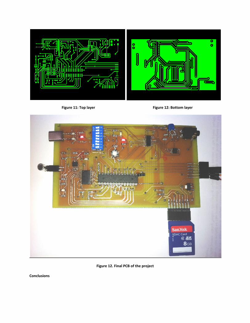
Figure 11: Top layer Figure 12: Bottom layer
Figure 12. Final PCB of the project
Conclusions

The project worked well under the circumstances. The operational amplifier picked up a lot of noise from the
microphone and thus the ADC conversions became moot. Hence we fed some external analog signal to the ADC
and able to capture those signals with little quantization error due to the 2 LSB bits getting stuck at 01. The rest of
the board performed well and as expected. The DAC output was fine and didn’t require extra testing. We were
able to play a song out through it successfully. Overall, the project performed as expected and we have a
successful output.
References
[1] Adv LinCMOS High-Speed 8-Bit A-to-D Converters Using Modified Flash Techniques (Rev. A)
http://www.ti.com/lit/gpn/tlc0820a
[2] 8-Bit Multiplying Digital-to-Analog Converters
http://www.ti.com/lit/gpn/tlc7524
[3] SD card interface with Arduino
http://www.arduino.cc/cgi-bin/yabb2/YaBB.pl?num=1206874649/8


