

Bipolar Conductance Switching of Single
Anthradithiophene Molecules
Bogdana Borca,∗,†,⊥ Verena Schendel,†,⊥ Remi Petuya,‡ Ivan Pentegov,†
Tomasz Michnowicz,† Ulrike Kraft,† Hagen Klauk,† Andres Arnau,¶,‡ Peter
Wahl,†,§ Uta Schlickum,∗,† and Klaus Kern†,∥
†Max-Planck-Institute for Solid State Research, 70569 Stuttgart, Germany
‡Donostia International Physics Centre, E-20018 Donostia - San Sebastian, Spain
¶Departamento de Fisica de Materiales UPV/EHU and CFM Donostia, Centro Mixto
CSIC-UPV/EHU, E-20018 Donostia - San Sebastian, Spain
§SUPA, School of Physics and Astronomy, University of St Andrews, North Haugh, St
Andrews, KY16 9SS, United Kingdom
∥Institut de Physique de la Matiere Condensee, Ecole Polytechnique Federale de Lausanne
(EPFL), CH-1015 Lausanne, Switzerland
⊥Equal contribution
E-mail: [email protected]; [email protected]
Phone: +49 (0)711 689-1539. Fax: +49 (0)711 689-1662
Abstract
Single molecular switches are basic device elements in organic electronics. The
pentacene analog anthradithiophene (ADT) shows a fully reversible binary switching
between different adsorption conformations on a metallic surface induced by a charge
transfer. These transitions are activated locally in single molecules in a low tempera-
ture Scanning Tunneling Microscope (STM). The switching induces changes between
1

bistable orbital structures and energy level alignment at the interface. The most stable
geometry, the “off” state, which all molecules adopt upon evaporation, corresponds
to a short adsorption distance at which the electronic interactions of the acene rings
bend the central part of the molecule towards the surface accompanied by a significant
charge transfer from the metallic surface to the ADT molecules. This leads to a shift
of the lowest unoccupied molecular orbital (LUMO) down to the Fermi level (EF ). In
the “on” state the molecule has a flat geometry at a larger distance from the surface,
consequently the interaction is weaker, resulting in a negligible charge transfer with an
orbital structure resembling the highest occupied molecular orbital (HOMO) when im-
aged close to the EF . The potential barrier between these two states can be overcome
reversibly by injecting charge carriers locally into individual molecules. Voltage con-
trolled current traces show a hysteresis characteristic of a bipolar switching behavior.
The interpretation is supported by first principles calculations.
Keywords
cis/trans ADT isomers, Cu(111), STM, DFT, conformational and electronic switches
A visionary perspective of molecular electronics is the use of single molecules as func-
tional entities in electronic devices.1 In this context, important components are molecular
switches,2,3 which can be interconverted reversibly between two or more stable states. Scan-
ning Tunneling Microscopy and Spectroscopy (STM/STS) represents an ideal tool to charac-
terize and manipulate single atoms and molecules on surfaces.4 Several switching mechanisms
have been explored previously with molecular and submolecular resolution and have been
induced locally by tunneling electrons,5–23 by an applied electric field24,25 or by combined
stimuli26–28 in the STM tunneling junction. Changes of the molecular configurations were
identified as changes of the folding in complex organic molecules,5 different types of isomer-
ization processes,7,13,15,18–24,28 changes of the atomic position in metal-organic complexes,6,26
2

formation and dissociation of chemical bonds.8–11,16,17,25 These conformational changes may
be accompanied by charging and discharging processes.12–16,27,28 Recently, another scenario
was proposed theoretically in which a switching process of an individual molecule is re-
lated to bistable electronic states. These are associated with different bonding strengths
and hybridization degrees of the molecules to a metallic substrate, resulting in a change
of the bending of the molecular conformation concomitant with a change of the adsorption
distance.29
In this study, we focus on single molecular switches consisting of individual anthradithio-
phene (ADT) molecules. ADT is a structural analog of pentacene, with two sulfur contain-
ing groups at each molecular terminal side representing cis and trans diastereomers.30 The
switching of individual molecules is activated locally by injecting charge carriers from the
STM tip apex into the molecule. The molecules are reversibly interconverted by bipolar
voltage pulses between two different adsorption geometries that correspond to two different
electronic conformations of the molecule. The characteristic parameter responsible for the
structural and electronic changes is the adsorption distance that determines the bonding
strength and the degree of hybridization between the ADT molecule and the surface, sim-
ilar to the recently proposed case of benzene derivatives.29 Our first-principles calculations
using van der Waals density functionals where exchange and correlation are treated con-
sistently (vdW-DF-cx),31,32 allow us to propose a model based on the appearance of two
adsorption states corresponding to two different geometric (bent and planar) and electronic
conformations. These two conformations are induced by two main driving forces, the S-Cu
bond length and the adsorption constraint for an optimal binding of the acene groups to the
substrate, similar to pentacene.33,34
3

Results and discussion
Individual ADT molecules deposited at 200K on the Cu(111) surface, adsorb with their
long axis along the high symmetry directions of the substrate, where cis and trans isomers
adopt the same adsorption conformation (Figure 1 a). In topographic images acquired with
a metallic tip the two isomers are practically indistinguishable and all molecules appear in a
“dumbbell-like” shape. Functionalizing the STM tip with a single ADT molecule (by picking
up the encircled molecule in Figure 1 a) the orbital structure can be resolved (Figure 1 b) and
thus the cis and trans diastereomers can be identified. Different configuration characteristic
for each isomer at the molecular extremities, with higher charge density on the same side
(cis) or to the opposite side (trans) are observed, as indicated by the arrows in Figure 1
(c, d).
Placing the tip above the center of the molecules, as shown in Figure 2 (a, b), a negative
voltage pulse of -0.5V was applied. During this measurement the feedback loop was opened
and the tunneling current recorded. After a certain time, an abrupt change in the tunneling
current, i.e., a step-like (for cis-ADT) and a double step-like (for trans-ADT) behavior
is observed (Figure 2 c, d). Rescanning the same molecules reveals that the increase in
the current is associated with a change in the topographic appearance (Figure 2 a, b). In
addition, in the switched conformation the trans-ADT molecule is rotated by about 10◦
(Figure 2 b), which can be related to the double step feature in the current trace (Figure 2
d). Switching the molecule back to the initial state is induced by a positive voltage (Figure
2 c, d lower panel). In the following, we will refer to the initial adsorption conformation as
the “off” state, and the conformation related to a higher conductance (in open feedback-loop
conditions) as the “on” state.
The measurements suggest that the two different adsorption conformations of ADT
molecules rely on the interplay between the S containing groups and the acene group posi-
tion with respect to the Cu substrate atoms. In Figure 2 (a, b upper panels) ball-and-stick
models for both adsorption conformations on Cu(111) are represented in a top view for both
4

Figure 1: a) 30x20 nm2 STM topography acquired in constant current mode (I=100 pA,V=100mV). ADT molecules are oriented along the high symmetry directions of the Cu(111)surface. The encircled molecule was used to functionalize the tip by vertical manipulation.b) Isomer-resolved STM image obtained with the functionalized tip of the same area as (a)in constant height (∼ 5 A above the surface, V=10mV) . Guiding lines are drawn for eachmolecular configuration. (c, d) Enlarged resolution images of the two ADT molecules framedin (b), represent the cis-ADT and trans-ADT isomers. Guiding arrows are drawn at themolecular extremities.
isomers. The acene group tends to have the benzene units centered over the hollow sites of
the surface, which favors alignment of the molecules along the high symmetry directions as
in the case of pentacene on Cu(111).35 In addition, there is a tendency of the S atoms of
the thiophene rings to sit on top of Cu atom positions.36 The cis-isomer has its acene rings
centered over the hollow sites and follows the high symmetry axis with the S atoms in atop
positions of the Cu(111) surface. Conversely, for the trans-isomer, when the acene rings
5

CuSCH
0 500 1000 1500 20001
2
3
4
5
0 500 10001
2
3
4
5back-switching
"on"
"on"
"off"
"off"
switching
+0.4V
I(n
A)
time (ms)
-0.5V
cis trans
10°5Å 5Å 5Å 5Å
a) b)
“on”“off” “on”“off”
c) d)
0 500 1000 1500 20001
2
3
4
5
0 500 10001
2
3
4
5
6+0.7V back-switching + rotation
"on"
"on"
"off"
I(nA
)
time (ms)
"off"
switching + rotation
-0.5V
10°
Figure 2: (a,b) STM images of the cis-ADT isomer and trans-ADT isomer and the top viewof the ball-and-stick models representations on Cu(111), in the “off” and “on” conformation,respectively. Applying a negative bias pulse above the center of the molecules as indicated,implies switching to the “on” conformation. Trans-ADT isomers rotate by about 10◦ duringthe switching process. (c, d) Current monitored as a function of time for the switching andback-switching process in an open-loop configuration. Before the feedback was tuned off thetip was stabilized at 100mV and 100 pA. Subsequently the tip was approached by 1 A (and0.8 A for (d)-lower panel, respectively) towards the molecule’s center with the feedback-loop turned off. Upper panel: switching process of cis-ADT and trans-ADT isomers fromthe “off” state (lower conductance) to the “on” state (higher conductance), by applyinga negative bias voltage. Lower panel: back-switching from “on” to “off” conformation byapplying a positive bias voltage.
are centered over the hollow sites the S atoms cannot be in the same registry with Cu(111)
atoms of the surface. This suggest a reason for why the cis-isomers do not change the ad-
sorption position while the trans-isomers rotate, as shown in panel (b). DFT calculations of
the adsorption energy for both isomers and both conformations (“off” and “on” states) as a
function of the tilt angle of the molecules with respect to the surface symmetry axis show
minima at 0◦. For the trans-isomer in the “on” state a small energy barrier for a rotation
by about 10◦, has to be overcome. (Supplementary Information)
The detailed electronic density of states of the molecular conformations is summarized
in Figure 3. Using an STM tip functionalized with an ADT molecule, the orbital structures
6

Molecule “off“ Molecule “on“
5 Å I =100 pA,
V =5 mV
I =100 pA, V=100 mV
V =5 mV5 Å 5 Å
a)
c) d)
b)
5 Å
LUMO HOMOf)e)
V=100 mV
Figure 3: (a,b) STM topographic images of a cis-ADT molecule in “off” and “on” confor-mations, respectively. (c, d) Constant height images resolving the orbital structures of the“off” and “on”conformations, resembling the LUMO and HOMO of a free molecule in thegas phase as shown in the (e) and (f) panels.
of both conformations (“off” and “on”) close to the Fermi level of the substrate (recorded
at 5mV) are resolved (Figure 3 c,d). Comparing the images with the molecular orbitals
calculated for the free molecule in the gas phase reveals that the states near the EF in
the “off” state resemble the lowest unoccupied molecular orbital (LUMO), whereas in the
“on” state they resemble the highest occupied molecular orbital (HOMO). This observation
suggests that the switching between the two conformations is related to a charge transfer
accompanied by a shift of the molecular orbitals. This behavior during the switching process,
which is related to changes of the alignment of the energy levels, is obtained for both isomers.
The only difference, as pointed out already, is the additional in-plane rotation in the case
of the trans-ADT. Thus, the switching mechanism itself is similar for both isomers and for
simplicity we will focus in the following on the cis-ADT.
To obtain a clear understanding of these two molecular conformations, DFT calculations
of the electronic structure of the molecule-substrate system varying the adsorption distance,
were performed. As described below, the bent adsorption geometry of the ADT in the “off”
7

2.2 2.3 2.4 2.5 2.6 2.7 2.8 2.9 3.0 3.1 3.2 3.3-1.75-1.70-1.65-1.60-1.55-1.50-1.45-1.40-1.35
1.5 2.0 2.5 3.0 3.5 4.0 4.5 5.0 5.5 6.0-2.0-1.5-1.0-0.50.00.51.01.52.0
-Ead
(eV
)
z (Å)
vdW-DF-cx
a)
b)
z=2.5 Å z=2.8 Å
c)LUMO
Figure 4: a) Adsorption energy −Ead of the cis-ADT isomer as a function of the adsorptionheight z on Cu(111) from vdW-DF-cx calculations. Lower panel: close-up around the minimaof the adsorption curve. Insets: side view of the optimized geometries of the ADT moleculeat the two adsorption heights z=2.5 A and z=2.8 A , where the two minima in −Ead appear,corresponding to the “off” and “on” conformations, respectively. b) The PDOS calculatedat the molecular adsorption distance of z=3.25 A , z=3 A , z=2.8 A and z=2.5 A highlightsshifts of the LUMO decreasing the distance to the surface, as indicated by arrows. A partialfilling of the LUMO orbital is obtained for the molecule in the “off” conformation at z=2.5 A .c) Calculated molecular appearances at the corresponding distance above the surface. Thegeometry for adsorption distances of z=3 A and z=3.25 A are not fully optimized.
state permits a closer adsorption distance, as compared to the planar case in the “on” state,
that leads to a rather strong hybridization between the ADT molecule’s π-cloud and the
Cu(111) metal surface, enough to compensate the Pauli repulsion and the energy penalty for
the geometrical distortion. The calculations reveal two minima for the adsorption energies
at z=2.5 A and z=2.8 A separated by a shallow energy barrier as shown in Figure 4 (a).
These two minima appear after relaxing the (X,Y,Z) coordinates of the S atoms and the
(X,Y) coordinates of the C and H atoms. The corresponding fully optimized molecular
conformations with full relaxations of all atoms in (X,Y,Z) coordinates are indicated in the
8

inset of Figure 4(a).
In the molecular state at z=2.5 A , the “off” conformation, the molecule is adsorbed with
the acene rings slightly closer to the surface compared to the S-Cu distance, which gives
rise to the “dumbbell-like” appearance in the STM topographic images. This geometry
corresponds to an adsorption state with a strong hybridization between the ADT molecule
and the Cu(111) substrate that includes a significant amount of charge transfer to the LUMO
of about one electron. By these means, the LUMO broadens and shifts to lower energies,
thus closer to the Fermi energy, as visible in the projected density of states (PDOS) in Figure
4 (b). The “off” state is the ground state of the molecule, consistent with the experimental
observation where molecules are only found in the “off” state after deposition.
In the “on” state the interaction between the ADT molecule and the Cu(111) substrate
is weaker and corresponds to an adsorption state with a planar molecular geometry at larger
distance of the acene rings from the surface. Here, no significant charge transfer between
the surface and the molecule is present and the LUMO is essentially unoccupied as shown
in the calculated PDOS (Figure 4 b). By increasing the distance between the molecule and
the surface, the LUMO shifts further towards higher energies. In both, the “on” and the
“off” state, a hybridization between the ADT molecular orbitals and Cu(111) surface states
exists. However, the dependence of the hybridization and the mixing of the HOMO-LUMO
orbitals decreases by increasing the molecular adsorption distance. These theoretical findings
support the experimental observations. In the “off” state the LUMO shifts down to the Fermi
energy, whereas in the “on” state, the LUMO is shifted to higher energies. The exact energy
positions of the HOMO and LUMO molecular orbitals with respect to the metal states
is difficult to accurately describe by DFT. The calculations still show a contribution of the
LUMO at the Fermi level of the substrate even for an adsorption distance of z=2.8 A (Figure
4 c). However, the shift of the LUMO to higher energies with the adsorption distance is well
described, supporting the experimental findings. A schematic representation of the alignment
of the energy levels, based on the calculated PDOS, in the two conformations and for both
9
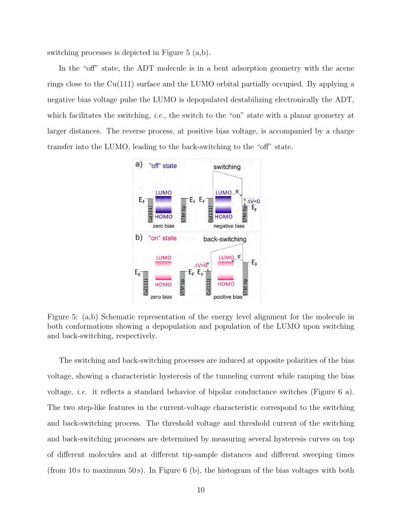
switching processes is depicted in Figure 5 (a,b).
In the “off” state, the ADT molecule is in a bent adsorption geometry with the acene
rings close to the Cu(111) surface and the LUMO orbital partially occupied. By applying a
negative bias voltage pulse the LUMO is depopulated destabilizing electronically the ADT,
which facilitates the switching, i.e., the switch to the “on” state with a planar geometry at
larger distances. The reverse process, at positive bias voltage, is accompanied by a charge
transfer into the LUMO, leading to the back-switching to the “off” state.
Figure 5: (a,b) Schematic representation of the energy level alignment for the molecule inboth conformations showing a depopulation and population of the LUMO upon switchingand back-switching, respectively.
The switching and back-switching processes are induced at opposite polarities of the bias
voltage, showing a characteristic hysteresis of the tunneling current while ramping the bias
voltage, i.e. it reflects a standard behavior of bipolar conductance switches (Figure 6 a).
The two step-like features in the current-voltage characteristic correspond to the switching
and back-switching process. The threshold voltage and threshold current of the switching
and back-switching processes are determined by measuring several hysteresis curves on top
of different molecules and at different tip-sample distances and different sweeping times
(from 10 s to maximum 50 s). In Figure 6 (b), the histogram of the bias voltages with both
10

polarities is plotted, corresponding to the “on” state and to the “off” state switching. In
Figure 6 (c), the distribution of the current values for both switching processes is represented.
A broader range of voltage values are observed for the switching events at negative polarity,
while for the back-switching at positive bias polarity, the distribution of current values is
broader. This slightly different distribution range of voltage and current for the switching
and back-switching processes are related to different switching mechanisms attributed to the
depopulation and population of the LUMO orbital. The bipolar switching process, where
switching takes place at negative energies and back-switching at positive ones, is confined
within an energy range of ±0.6V (for moderate tunnel parameters, i.e. currents no larger
than approximately 20 nA). Beyond that energy window, for instance at -0.8V, current
fluctuations associated with a toggling between the two states are observed. However, the
switching mechanisms involved at those energies differ from those responsible for the bipolar
switching. The current fluctuations show that the “off” state is energetically more favorable
as the occupation time of the molecule in the “off” state is much higher compared to the
occupation time of the molecule in the “on” state (Supplementary Information).
To confirm that the “on” conformation is the metastable state we have tracked the
duration of the “on” state of the cis molecules over time. Figure 7 shows the percentage of
the cis molecules in the “on” state which decreases exponentially in time with a decay time
of about 7 hours.
The switching and back-switching processes correspond to electronic transitions accom-
panied by conformational changes between two different potential energy surfaces. These
energy surfaces are defined by the Marcus parabolas of the corresponding diabatic states,37
similar to the case of metal atoms adsorbed on thin NaCl buffer layer grown on metal sur-
faces.38 However, in our case the conformational changes occur at the molecular level of
individual ADT molecules, which possess many degrees of freedom and, thus, allow for the
existence of the two above mentioned adsorption states: a bent geometry with the acene
rings at closer distances, in which the optimal π-bonding length of the central acene rings
11

0 5 10 15 200
10
20
30
co
un
ts
I(nA)0 5 10 15 20
0
10
20
30
co
un
ts
-0.6 -0.4 -0.2 0.0 0.2 0.4 0.60
10
20
30
bias (V)
b) switching back-switching
c)
-0.6 -0.4 -0.2 0.0 0.2 0.4 0.6
-5
-4
-3
-2
-1
0
1
2
bias (V)
I(n
A)
"off"
"on"
a)
0 5 10 15 200
10
20
30
counts
counts
I(nA)
-0.6 -0.4 -0.2 0.0 0.2 0.4 0.60
10
20
30
bias (V)
0 5 10 15 200
10
20
30
b)
c)
Figure 6: a) Bipolar switching and back-switching hysteresis recorded by positioning theSTM tip over the center of a cis-ADT isomer in the “off” conformation. The I(V ) curveswere recorded as the bias voltage was ramped, with the feedback turned off, from 0.6V to-0.6V and back as indicated by arrows in corresponding colors. The two step-like features inthe current traces correspond to the switching and back-switching process. b) Bias voltagehistograms with a bin of 50mV corresponding to the switching (mean value −0.44± 0.1V)and back-switching (mean value +0.4± 0.04V) processes, evaluated from several hysteresiscurves taken above different molecules, at different tip-sample distances and with differentsweeping times (from 10 s to maximum 50 s). c) Current histograms of the switching (meanvalue 2.52± 1.88 nA) and back-switching (mean value 6.06± 3.68 nA) processes.
compensates for the energy cost of the distortion imposed by the constraint of the S-Cu
bond distance of the S-containing end groups, and a planar geometry at larger distances
of the acene rings above the surface and optimal S-Cu bond distances. The optimal ad-
sorption distance between the central acene groups and the Cu(111) surface is very close to
the pentacene-Cu(111) adsorption distance.33,34 However, the presence of S atoms in both
end groups of the ADT molecule imposes an additional constraint due to the longer S-Cu
bonding distance. The combination of both effects results in the two adsorption geometries,
a bent geometry (“off” state) in which energy costs of the deformation is compensated by the
12

0 4 8 12 16 200
20
40
60
80
100
Mole
cule
sin
"On"
state
(%)
Time (hours)
decay time= 6.78 ± 0.38 hours 13h 40 min
10nm 10nm
a) b)
Figure 7: a) Exponential decay time of the molecules from the “on” to the “off” state. b)The corresponding STM images acquired in constant current mode (I=40pA, V=50mV)with several molecules in “on” state and after they are switched to the “off” state.
optimal π-bonding of the acene groups to the metal surface, and a planar geometry (“on”
state) without energy penalty for the geometrical distortion but with a longer bond length
due to the S-Cu constraint. A similar behavior is described in the case of chlorinated benzene
derivatives, as discussed in Ref. [29], but not in the case of pentacene. In this latter case there
are no additional atoms, like the S atoms of ADT or the Cl atoms of benzene derivatives,
introducing constraints to the optimal adsorption geometries. Therefore, it is the molecular
flexibility which allows the molecule to possess the two different bonding conformations to
the metal surface, accompanied by changes of the molecular orbital occupations.
Conclusion
In conclusion, we have demonstrated reversible bipolar conductance switching of single ADT
molecules adsorbed on Cu(111) and induced locally in a fully controlled manner in the STM
tunneling junction. The comparison of the orbital resolved STM images with DFT calcu-
lations reveals that the switching process is accompanied by a geometric and an electronic
change induced by charge transfer at the metal-organic interface associated with the depop-
ulation and population of the LUMO orbital. These findings may be transferred to potential
13

storage bits, allowing for controlled switching to “on” and “off” states at the individual
molecular level.
Experimental and computational methods
The experiments were performed under ultra-high vacuum conditions (UHV) with a home-
built low temperature Scanning Tunneling Microscope (LT-STM) operating at a temperature
of 6K. The single Cu(111) crystal was prepared by repeated cycles of Ar+ ion sputtering and
subsequent annealing. A mixture of cis :anthra[2,3-b:7,6-b’]dithiophene and trans :anthra[2,3-
b:6,7-b’]dithiophene isomers were sublimated with an Organic Molecular Beam Deposition
technique on the Cu(111) surface with a submonolayer coverage. ADT molecules were pur-
chased from Sigma-Aldrich. To prevent the molecules from reacting at the surface, the
substrate is held at 200K during deposition. Subsequently, the sample is transferred in situ
to the LT-STM. Bias voltages are applied to the sample. The STM measurements were
performed both in constant current and constant height modes.
The DFT-vdW calculations were done using the VASP code.39,40 The ADT/Cu(111)
system was modelled using a 8x4 Cu(111) periodic supercell with four Cu layers, the ion-
electron interaction was described with the Projector Augmented-Wave (PAW) method,41
whereas the exchange and correlation potential was taken into account by the Generalized
Gradient Approximation(GGA)42 and including the vdW dispersion forces using the vdW-
DF-cx method.31,32 In the plane wave expansion we consider a kinetic energy cut-off of
500 eV. To satisfy the summations in the reciprocal space for the Brillouin zone a mesh of
2×3 k points in the 1×1 unit cell was chosen. For all calculations the electronic convergence
criterion was 1× 10⁻⁴ eV, while the convergence on forces in the relaxation was 0.05 eV/A.
14

Acknowledgement
We acknowledge funding by the Emmy-Noether-Program of the Deutsche Forschungsgemein-
schaft, the SFB 767, and the Baden-Wurttemberg Stiftung. R.P. and A.A. thank the basque
Departamento de Universidades e Investigacion (grant No. IT-756-13) and the spanish Min-
isterio de Economia y Competitividad (grant No. FIS2013-48286-C2-8752-P) for financial
support. R.P. and A.A. also acknowledge Joakim Lofgren and Per Hyldgaard for stimulating
discussions about the vdW-DF-cx implementation.
Supporting Information Available
This material is available free of charge via the Internet at http://pubs.acs.org/.
References
1. Van der Molen, S. J.; Naaman, R.; Scheer, E.; Neaton, J. B.; Nitzan, A.; Natelson, D.;
Tao, N.; Van der Zant, H.; Mayor, M.; Ruben, M. et al. Visions for a Molecular Future.
Nat. Nanotechnol. 2013, 8, 385–389.
2. Kay, E. R.; Leigh, D. A.; Zerbetto, F. Synthetic Molecular Motors and Mechanical
Machines. Angew. Chem., Int. Ed. 2007, 46, 72–191.
3. Feringa, B. L.; Browne, W. R. Molecular Switches (2nd Edition); Wiley-VCH: WEIN-
HEIM, 2011; pp 1–792.
4. Eigler, D. M.; Schweizer, E. K. Positioning Single Atoms with a Scanning Tunnelling
Microscope. Nature 1990, 344, 524–526.
5. Iancu, V.; Hla, S.-W. Realization of a Four-Step Molecular Switch in Scanning Tunneling
Microscope Manipulation of Single Chlorophyll Molecules. Proc. Natl. Acad. Sci. 2006,
103, 13718–13721.
15

6. Wang, Y.; Kroger, J.; Berndt, R.; Hofer, W. A. Pushing and Pulling a Sn Ion through
an Adsorbed Phthalocyanine Molecule. J. Am. Chem. Soc. 2009, 131, 3639–3643.
7. Fu, Y.-S.; Schwobel, J.; Hla, S.-W.; Dilullo, A.; Hoffmann, G.; Klyatskaya, S.; Ruben, M.;
Wiesendanger, R. Reversible Chiral Switching of Bis(phthalocyaninato) Terbium(III) on
a Metal Surface. Nano Lett. 2012, 12, 3931–3935.
8. Ohmann, R.; Vitali, L.; Kern, K. Actuated Transitory Metal - Ligand Bond As Tunable
Electromechanical Switch. Nano Lett. 2010, 10, 2995–3000.
9. Albrecht, F.; Neu, M.; Quest, C.; Swart, I.; Repp, J. Formation and Characterization
of a Molecule-Metal-Molecule Bridge in Real Space. J. Am. Chem. Soc. 2013, 135,
9200–9203.
10. Mohn, F.; Repp, J.; Gross, L.; Meyer, G.; Dyer, M. S.; Persson, M. Reversible Bond
Formation in a Gold-Atom-Organic-Molecule Complex as a Molecular Switch. Phys.
Rev. Lett. 2010, 105, 266102.
11. Leung, L.; Lim, T.; Polanyi, J. C.; Hofer, W. A. Molecular Calipers Control Atomic
Separation at a Metal Surface. Nano Lett. 2011, 11, 4113–4117.
12. Swart, I.; Sonnleitner, T.; Repp, J. Charge State Control of Molecules Reveals Modi-
fication of the Tunneling Barrier with Intramolecular Contrast. Nano Lett. 2011, 11,
1580–1584.
13. Walch, H.; Leoni, T.; Guillermet, O.; Langlais, V.; Scheuermann, A.; Bonvoisin, J.;
Gauthier, S. Electromechanical Switching Behavior of Individual Molecular Complexes
of Cu and Ni on NaCl-Covered Cu(111) and Ag(111). Phys. Rev. B 2012, 86, 075423.
14. Fu, Y.-S.; Zhang, T.; Ji, S.-H.; Chen, X.; Ma, X.-C.; Jia, J.-F.; Xue, Q.-K. Identifying
Charge States of Molecules with Spin-Flip Spectroscopy. Phys. Rev. Lett. 2009, 103,
257202.
16
15. Leoni, T.; Guillermet, O.; Walch, H.; Langlais, V.; Scheuermann, A.; Bonvoisin, J.;
Gauthier, S. Controlling the Charge State of a Single Redox Molecular Switch. Phys.
Rev. Lett. 2011, 106, 216103.
16. Uhlmann, C.; Swart, I.; Repp, J. Controlling the Orbital Sequence in Individual Cu-
Phthalocyanine Molecules. Nano Lett. 2013, 13, 777–780.
17. Riedel, D.; Bocquet, M.-L.; Lesnard, H.; Lastapis, M.; Lorente, N.; Sonnet, P.; Du-
jardin, G. Selective Scanning Tunnelling Microscope Electron-Induced Reactions of Sin-
gle Biphenyl Molecules on a Si(100) Surface. J. Am. Chem. Soc. 2009, 131, 7344–7352.
18. Liljeroth, P.; Repp, J.; Meyer, G. Current-Induced Hydrogen Tautomerization and Con-
ductance Switching of Naphthalocyanine Molecules. Science 2007, 317, 1203–1206.
19. Henzl, J.; Mehlhorn, M.; Gawronski, H.; Rieder, K.-H.; Morgenstern, K. Reversible Cis-
Trans Isomerization of a Single Azobenzene Molecule. Angew. Chem., Int. Ed. 2006,
45, 603–606.
20. Morgenstern, K. Isomerization Reactions on Single Adsorbed Molecules. Acc. Chem.
Res. 2009, 42, 213–223.
21. Kumagai, T.; Hanke, F.; Gawinkowski, S.; Sharp, J.; Kotsis, K.; Waluk, J.; Persson, M.;
Grill, L. Thermally and Vibrationally Induced Tautomerization of Single Porphycene
Molecules on a Cu(110) Surface. Phys. Rev. Lett. 2013, 111, 246101.
22. Simpson, G. J.; Hogan, S. W. L.; Caffio, M.; Adams, C. J.; Fruchtl, H.; van Mourik, T.;
Schaub, R. New Class of Metal Bound Molecular Switches Involving H-Tautomerism.
Nano Lett. 2014, 14, 634–639.
23. Parschau, M.; Passerone, D.; Rieder, K.-H.; Hug, H. J.; Ernst, K.-H. Switching the
Chirality of Single Adsorbate Complexes. Angew. Chem., Int. Ed. 2009, 48, 4065–4068.
17

24. Alemani, M.; Peters, M. V.; Hecht, S.; Rieder, K.-H.; Moresco, F.; Grill, L. Electric
Field-Induced Isomerization of Azobenzene by STM. J. Am. Chem. Soc. 2006, 128,
14446–14447.
25. Serrate, D.; Moro-Lagares, M.; Piantek, M.; Pascual, J. I.; Ibarra, M. R. Enhanced
Hydrogen Dissociation by Individual Co Atoms Supported on Ag(111). J. Phys. Chem.
C 2014, 118, 5827–5832.
26. Qiu, X. H.; Nazin, G. V.; Ho, W. Mechanisms of Reversible Conformational Transitions
in a Single Molecule. Phys. Rev. Lett. 2004, 93, 196806.
27. Wu, S. W.; Ogawa, N.; Ho, W. Atomic-Scale Coupling of Photons to Single-Molecule
Junctions. Science 2006, 312, 1362–1365.
28. Lee, J.; Tallarida, N.; Rios, L.; Perdue, S. M.; Apkarian, V. A. Single Electron Bipolar
Conductance Switch Driven by the Molecular Aharonov-Bohm Effect. ACS Nano 2014,
8, 6382–6389.
29. Liu, W.; Filimonov, S. N.; Carrasco, J.; Tkatchenko, A. Molecular Switches from Benzene
Derivatives Adsorbed on Metal Surfaces. Nat. Commun. 2013, 4, 3569.
30. Anthony, J. E. Functionalized Acenes and Heteroacenes for Organic Electronics. Chem.
Rev. 2006, 106, 5028–5048.
31. Berland, K.; Hylgaard, P. Exchange Functional that Tests the Robustness of the Plasmon
Description of the Van der Waals Density Functionals. Phys. Rev. B 2014, 89, 035412–1,
035412–8.
32. Bjorkman, T. Testing Several Recent van der Waals Density Functionals for Layered
Structures. J. Chem. Phys. 2014, 141, 074708–1, 074708–6.
18
33. Toyoda, K.; Nakanoa, Y.; Hamada, I.; Lee, K.; Yanagisawa, S.; Morikawa, Y. First-
Principles Study of the Pentacene/Cu(1 1 1) Interface: Adsorption States and Vacuum
Level Shifts. J. Electron Spectrosc. Relat. Phenom. 2009, 174, 78–84.
34. Koch, N.; Gerlach, A.; Duhm, S.; Glowatzki, H.; Heimel, G.; Vollmer, A.; Sakamoto, Y.;
Suzuki, T.; Zegenhagen, J.; Rabe, J. P. et al. Adsorption-Induced Intramolecular Dipole:
Correlating Molecular Conformation and Interface Electronic Structure. J. Am. Chem.
Soc. 2008, 130, 7300–7304.
35. Lagoute, J.; Kanisawa, K.; Folsch, S. Manipulation and Adsorption-Site Mapping of
Single Pentacene Molecules on Cu(111). Phys. Rev. B 2004, 70, 245415.
36. Milligan, P.; Namarra, J. M.; Murphy, B.; Cowie, B.; Lennon, D.; Kadodwala, M. A
NIXSW and NEXAFS Investigation of Thiophene on Cu(111). Surf. Sci. 1998, 412413,
166 – 173.
37. Marcus, R. A. Electron Transfer Reactions in Chemistry. Theory and Experiment. Rev.
Mod. Phys. 1993, 65, 599–610.
38. Olsson, F. E.; Paavilainen, S.; Persson, M.; Repp, J.; Meyer, G. Multiple Charge States
of Ag Atoms on Ultrathin NaCl Films. Phys. Rev. Lett. 2007, 98, 176803.
39. Kresse, G.; Hafner, J. Ab Initio Molecular-Dynamics Simulation of the Liquid-Metal-
Amorphous-Semiconductor Transition in Germanium. Phys. Rev. B 1994, 49, 14251–
14269.
40. Kresse, G.; Furthmuller, J. Efficient Iterative Schemes for Ab Initio Total-Energy Cal-
culations Using a Plane-Wave Basis Set. Phys. Rev. B 1996, 54, 11169–1118.
41. Blochl, P. E. Projector Augmented-Wave Method. Phys. Rev. B 1994, 50, 17953–17979.
42. Perdew, J. P.; Burke, K.; Ernzerhof, M. Generalized Gradient Approximation Made
Simple [Phys. Rev. Lett. 77, 3865 (1996)]. Phys. Rev. Lett. 1997, 78, 1396–1396.
19

Graphical TOC Entry
20

_________________________________________________________
*To whom correspondence should be addressed, ⊥Equal contribution
†Max-Planck-Institute for Solid State Research, 70569 Stuttgart, Germany
‡Donostia International Physics Centre, E-20018 Donostia - San Sebastián, Spain
¶Departamento de Fisica de Materiales UPV/EHU and CFM Donostia, Centro Mixto CSIC-
UPV/EHU, E-20018 Donostia - San Sebastián, Spain §SUPA, School of Physics and Astronomy, University of St Andrews, North Haugh, St Andrews,
KY16 9SS, United Kingdom ∥Institut de Physique de la Matière Condensée, École Polytechnique Fédérale de Lausanne
(EPFL), CH-1015 Lausanne, Switzerland
Supplementary Information
Bipolar Conductance Switching of Single
Anthradithiophene Molecules
Bogdana Borca,∗,†,⊥ Verena Schendel,
†,⊥ Rémi Pétuya,
‡ Ivan Pentegov,
† Tomasz
Michnowicz,† Ulrike Kraft,
† Hagen Klauk,
† Andrés Arnau,
¶,‡ Peter Wahl,
†,§ Uta
Schlickum,∗,† and Klaus Kern
†,∥
Analysis of switching behavior in time traces
Anthradithiophene (ADT) molecular switches are interconverted between the bistable states
corresponding to different adsorption conformations on the surface by a bias voltage with
opposite polarities applied locally on individual molecules underneath the STM tip. The
corresponding I(V) curves show characteristic hysteretic behavior. Predominantly the switching
from the “off” to the “on” state occurs at negative voltage polarity applied to the sample and the
back-switching at positive polarity. For the negative polarity of the applied voltage with absolute
values higher than -0.6 V, both transitions may occur. For positive polarity of the applied
voltage, a current higher than 20 nA cause the appearance of switching and back-switching
transitions. At these parameters of instability, the current traces show step-like transitions
corresponding to the switching and the back-switching processes, the so-called telegraphic noise
behavior. In Figure S1 a), we represent two current traces recorded at -0.8 V and +0.4 V
respectively, for which these transitions between the “off” and “on” states arise. The spectra
reveal a much longer lifetime of the system in the “off” state as compared to the lifetime in the
“on” state as revealed by the current histograms Figure S1 (b), which is consistent with the fact
that the “off” state is found as the ground state and the “on” state as a metastable state, in
agreement with our DFT calculations.

2
Figure S1 a) Current traces recorded at -0.8 V and +0.4 V with open feedback loop. b)
Histograms of the current traces in panel (a).
Adsorption energy as function of tilt angle
The adsorption conformations of ADT molecules rely on the interplay between the sulfur
containing groups and the acene group position with the substrate atoms. Figure S2 summarizes
the analysis of the adsorption energy for both isomers and both conformations at z=2.50 Ả (“off”
state) and z=2.80 Ả (“on” state) as a function of the tilt angle of the molecules with respect to the
surface symmetry axis. The acene group tends to have the benzene units centered over the
hollow sites of the surface, which favors the alignment of the molecules along the high symmetry
directions, particularly at short distances to the surface when the ADT molecules are in the “off”
state and in a stronger interaction with the surface. In these conditions the adsorption curves
show clear minima at 0° tilt angle for both isomers (Figure S2 a). However, there is an additional
effect due to the tendency of the sulfur atoms of the thiophene rings to adopt atop positions that
reinforces the alignment for the cis-isomer but tends to rotate the ADT in the case of the trans-
isomer, the balance being very delicate as shown in the right panel of Figure S2 (a). A ball-and-
stick model of both isomers is drawn in Figure S2 (b,c) for 0° and 9° tilt angle, respectively .
As a consequence of these two competing effects, in the “on” state, the cis-isomer has an energy
barrier of 200 meV for the rotation higher by a factor of four than that of the trans-isomer which
is only 50 meV. These findings explain why only the trans-isomer rotates during the switching
process. However, such a delicate balance is not fully reproduced by our DFT calculations with a
steepest minimum at 0° tilt angle instead of 9° for the trans-isomer at z=2.80 Ả (in the “on”
state).

3
Figure S2 a) Adsorption energy −Ead of the
cis-ADT and trans-ADT isomers as a
function of the tilt angle in the two
adsorption states: “off” state at z=2.50 Ả
and “on” state at z=2.80 Ả. The arrows
mark the energy barriers for the rotation
that are 200/50 meV for the cis-/trans-
isomer, respectively. (b,c) Top view of the
cis-ADT (left panels) and trans-ADT (right
panels) in the equilibrium position at
z=2.80 Ả following the high symmetry
crystallographic axes of Cu(111) in (b) and
tilted by an angle of 9° around the sulfur
atom on top position on the left of the
molecule in (c).


