bq25700AACNVBUS
HIDRV1
SRN
VSYS
BATT(1S-4S)
BTST1BTST2LODRV1
SW1 SW2LODRV2
HIDRV2
SRP
BATDRVACP
SYS
Host
Q1Q2 Q3 Q4
Adapter 3.5V ± 24V
SM
Bus
IAD
PT
, IB
AT
, P
SY
S, P
RO
CH
OT
Copyright © 2017, Texas Instruments Incorporated
Product
Folder
Order
Now
Technical
Documents
Tools &
Software
Support &Community
An IMPORTANT NOTICE at the end of this data sheet addresses availability, warranty, changes, use in safety-critical applications,intellectual property matters and other important disclaimers. PRODUCTION DATA.
bq25700ASLUSCQ8A –MAY 2017–REVISED MAY 2018
bq25700A SMBus Multi-Chemistry Battery Buck-Boost Charge Controller With SystemPower Monitor and Processor Hot Monitor
1
1 Features1• Charge 1- to 4-Cell Battery From Wide Range of
Input Sources– 3.5-V to 24-V Input Operating Voltage– Supports USB2.0, USB 3.0, USB 3.1 (Type C),
and USB_PD Input Current Settings– Seamless Transition Between Buck and Boost
Operation– Input Current and Voltage Regulation (IDPM
and VDPM) Against Source Overload• Power/Current Monitor for CPU Throttling
– Comprehensive PROCHOT Profile, IMVP8Compliant
– Input and Battery Current Monitor– System Power Monitor, IMVP8 Compliant
• Narrow-VDC (NVDC) Power Path Management– Instant-On With No Battery or Deeply
Discharged Battery– Battery Supplements System When Adapter is
Fully-Loaded• Power Up USB Port From Battery (USB OTG)
– Output 4.48-V to 20.8-V Compatible With USBPD
– Output Current Limit up to 6.35 A• 800-kHz or 1.2-MHz Programmable Switching
Frequency for 1-µH to 3.3-µH Inductor• Host Control Interface for Flexible System
Configuration– SMBus (bq25700A) Port for Optimal System
Performance and Status Reporting– Hardware Pin to Set Input Current Limit
Without EC Control• Integrated ADC to Monitor Voltage, Current and
Power• High Accuracy Regulation and Monitor
– ±0.5% Charge Voltage Regulation– ±2% Input/Charge Current Regulation– ±2% Input/Charge Current Monitor– ±5% Power Monitor
• Safety– Thermal Shutdown– Input, System, Battery Overvoltage Protection– MOSFET Inductor Overcurrent Protection
• Low Battery Quiescent Current
• Input Current Optimizer (ICO) to Extract Max InputPower
• Charge Any Battery Chemistry: Li+, LiFePO4,NiCd, NiMH, Lead Acid
• Package: 32-Pin 4 × 4 WQFN
2 Applications• Ultra-Books, Notebooks, Detachable, Tablet PCs
and Power Bank• Industrial and Medical Equipment• Portable Equipment With Rechargeable Batteries
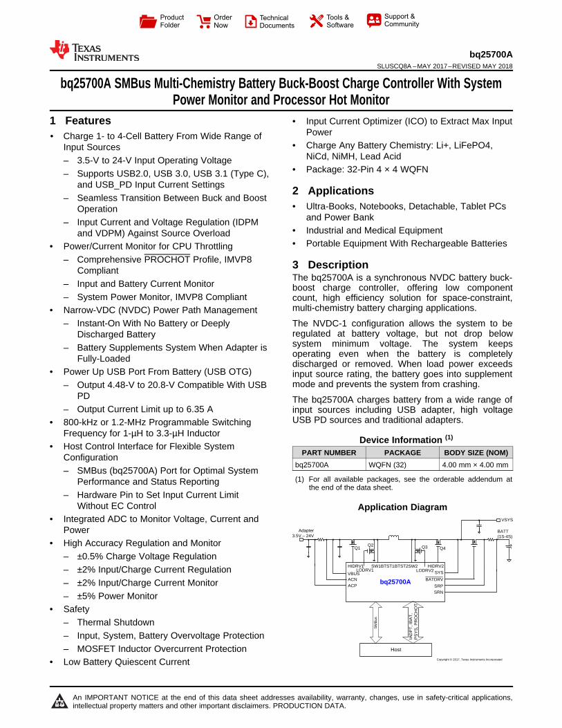
3 DescriptionThe bq25700A is a synchronous NVDC battery buck-boost charge controller, offering low componentcount, high efficiency solution for space-constraint,multi-chemistry battery charging applications.
The NVDC-1 configuration allows the system to beregulated at battery voltage, but not drop belowsystem minimum voltage. The system keepsoperating even when the battery is completelydischarged or removed. When load power exceedsinput source rating, the battery goes into supplementmode and prevents the system from crashing.
The bq25700A charges battery from a wide range ofinput sources including USB adapter, high voltageUSB PD sources and traditional adapters.
Device Information (1)
PART NUMBER PACKAGE BODY SIZE (NOM)bq25700A WQFN (32) 4.00 mm × 4.00 mm
(1) For all available packages, see the orderable addendum atthe end of the data sheet.
Application Diagram
2
bq25700ASLUSCQ8A –MAY 2017–REVISED MAY 2018 www.ti.com
Submit Documentation Feedback Copyright © 2017–2018, Texas Instruments Incorporated
Table of Contents1 Features .................................................................. 12 Applications ........................................................... 13 Description ............................................................. 14 Revision History..................................................... 25 Description (continued)......................................... 46 Pin Configuration and Functions ......................... 57 Specifications......................................................... 8
7.1 Absolute Maximum Ratings ...................................... 87.2 ESD Ratings ............................................................ 87.3 Recommended Operating Conditions....................... 87.4 Thermal Information .................................................. 97.5 Electrical Characteristics........................................... 97.6 Timing Requirements .............................................. 177.7 Typical Characteristics ........................................... 18
8 Detailed Description ............................................ 218.1 Overview ................................................................ 218.2 Functional Block Diagram ...................................... 228.3 Feature Description................................................. 238.4 Device Functional Modes........................................ 29
8.5 Programming .......................................................... 308.6 Register Map........................................................... 32
9 Application and Implementation ........................ 659.1 Application Information .......................................... 659.2 Typical Application .................................................. 65
10 Power Supply Recommendations ..................... 7211 Layout................................................................... 73
11.1 Layout Guidelines ................................................. 7311.2 Layout Example .................................................... 73
12 Device and Documentation Support ................. 7512.1 Device Support .................................................... 7512.2 Documentation Support ....................................... 7512.3 Receiving Notification of Documentation Updates 7512.4 Community Resources.......................................... 7512.5 Trademarks ........................................................... 7512.6 Electrostatic Discharge Caution............................ 7512.7 Glossary ................................................................ 75
13 Mechanical, Packaging, and OrderableInformation ........................................................... 76
4 Revision History
Changes from Original (May 2017) to Revision A Page
• Deleted Ideal Diode Operation in Supplement Mode from Features ..................................................................................... 1• Changed 2.2-µH to 3.3-µH and deleted Low Profile in Features .......................................................................................... 1• Added Integrated ADC to Monitor Voltage, Current and Power to Features ......................................................................... 1• Changed input source from being overloaded to system from crashing in Description ......................................................... 1• Changed 18.5 V for 3-cell, and 19.5 for 4-cell to 19.5 V for 3-cell/4-cell in CELL_BATPRESZ description .......................... 5• Changed I to O for CMPOUT I/O ........................................................................................................................................... 6• Changed V(IADP) to V(IADPT) in IADPT description ................................................................................................................... 6• Deleted minimum 10-ms and added minimum to PROCHOT description ............................................................................ 6• Changed REG0x3B to REG0x3D in VDPM_REG_ACC Test Conditions in Electrical Characteristics ........................................ 11• Changed REG0x3D to REG0x3B in VOTG_REG_ACC Test Conditions in Electrical Characteristics ........................................ 11• Changed REG0x12[15] = 0 to REG0x12[15] = 1 in Test Conditions for IBAT_BATFET_ON........................................................ 11• Changed REG0x12[15] = 0 to REG0x12[15] = 1 in Test Conditions for IBAT_BATFET_ON........................................................ 11• Changed IBATOVP test condition from: on SRP and SRN to: on VSYS pin............................................................................ 14• Added overbar to (BATDRV) in heading ............................................................................................................................. 16• Added overbar to PROCHOT in Overview .......................................................................................................................... 21• Changed 18.5V to 19.5V in 3S row SYSOVP column in Table 1 ....................................................................................... 23• Changed 0 to 0 A, lowside to low-side, and LSFET turn-on to LSFET turn-on when the HSFET is off in Continuous
Conduction Mode (CCM) ..................................................................................................................................................... 24• Changed Pulse Frequency Modulation (PFM) .................................................................................................................... 24• Changed during forward mode to during forward supplement mode in High-Accuracy Current Sense Amplifier
(IADPT and IBAT)................................................................................................................................................................. 25• Changed Processor Hot Indication ...................................................................................................................................... 26• Changed IADP to IADPT in Figure 13.................................................................................................................................. 27• Changed bq2570x to bq2570xA in Figure 14 ...................................................................................................................... 28• Added overbar to PROCHOT in PROCHOT Status ............................................................................................................ 28
3
bq25700Awww.ti.com SLUSCQ8A –MAY 2017–REVISED MAY 2018
Submit Documentation FeedbackCopyright © 2017–2018, Texas Instruments Incorporated
Revision History (continued)• Changed subscript of ILIM2_VTH in Input Overcurrent Protection (ACOC) .............................................................................. 28• Changed 3s – 18.5 V to 3s/4s – 19.5 V in System Overvoltage Protection (SYSOVP) ...................................................... 29• Added REG to Battery Charging ......................................................................................................................................... 29• Changed 0 mA – 6350 mA to 50 mA – 6400 mA for 3Fh in Table 6 .................................................................................. 33• Changed Device Address to DeviceID for FFh in Table 6 .................................................................................................. 33• Added <default at POR> to PWM_FREQ description in Table 7 ........................................................................................ 35• Added sentence to IBAT_GAIN description in Table 8 ....................................................................................................... 35• Changed LDO to internal resistor in EN_LDO description in Table 8 ................................................................................. 35• Deleted Independent Comparator Reference in Table 10 .................................................................................................. 36• Deleted Independent Comparator Polarity in Table 10 ....................................................................................................... 37• Deleted Independent Comparator Deglitch Time in Table 10 ............................................................................................. 37• Added independent to FORCE_LATCHOFF description in Table 10 ................................................................................. 37• Added <default at POR> to BATFETOFF_ HIZ description in Table 14 ............................................................................. 40• Added <default at POR> to PSYS_OTG_ IDCHG description in Table 14 ......................................................................... 40• Added PROCHOT Pulse Extension Enable to EN_PROCHOT_EXT description in Table 16 ............................................ 41• Added There is a 128 mA offset. to IDCHG_VTH description in Table 17 .......................................................................... 43• Changed 0 mA to 000000b in IDCHG_VTH description in Table 17 ................................................................................... 43• Changed text in ChargeCurrent Register (SMBus address = 14h) [reset = 0h] .................................................................. 49• Deleted text and changed larger to 20-mΩ in Input Current Registers ............................................................................... 54• Added paragraph to IIN_HOST Register With 10-mΩ Sense Resistor (SMBus address = 3Fh) [reset = 4000h] ............... 55• Changed Minimum System Voltage from 614 mV to 6144 mV in Design Requirements .................................................... 66• Deleted Input Snubber and Filter for Voltage Spike Damping section ................................................................................ 66
4
bq25700ASLUSCQ8A –MAY 2017–REVISED MAY 2018 www.ti.com
Submit Documentation Feedback Copyright © 2017–2018, Texas Instruments Incorporated
5 Description (continued)During power up, the charger sets converter to buck, boost or buck-boost configuration based on input sourceand battery conditions. The charger automatically transits among buck, boost and buck-boost configurationwithout host control.
In the absence of an input source, the bq25700A supports On-the-Go (OTG) function from 1- to 4-cell battery togenerate 4.48 V to 20.8 V on VBUS. During OTG mode, the charger regulates output voltage and output current.
The bq25700A monitors adapter current, battery current and system power. The flexibly programmed PROCHOToutput goes directly to CPU for throttle back when needed.
32S
W1
9IB
AT
1VBUS 24 HIDRV2
31H
IDR
V1
10P
SY
S2ACN 23 SW2
30B
TS
T1
11P
RO
CH
OT
3ACP 22 VSYS
29LO
DR
V1
12S
DA
4CHRG_OK 21 BATDRV
28R
EG
N13
SC
L5EN_OTG 20 SRP
27P
GN
D14
CM
PIN
6ILIM_HIZ 19 SRN
26LO
DR
V2
15C
MP
OU
T7VDDA 18 CELL_BATPRESZ
25B
TS
T2
16C
OM
P1
8IADPT 17 COMP2
Thermal
Pad
5
bq25700Awww.ti.com SLUSCQ8A –MAY 2017–REVISED MAY 2018
Submit Documentation FeedbackCopyright © 2017–2018, Texas Instruments Incorporated
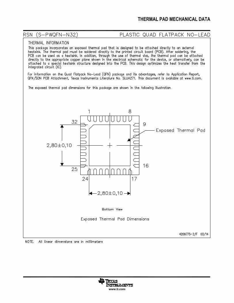
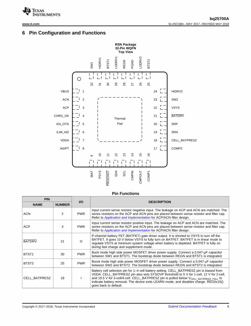
6 Pin Configuration and Functions
RSN Package32-Pin WQFN
Top View
Pin FunctionsPIN
I/O DESCRIPTIONNAME NUMBER
ACN 2 PWRInput current sense resistor negative input. The leakage on ACP and ACN are matched. Theseries resistors on the ACP and ACN pins are placed between sense resistor and filter cap.Refer to Application and Implementation for ACP/ACN filter design.
ACP 3 PWRInput current sense resistor positive input. The leakage on ACP and ACN are matched. Theseries resistors on the ACP and ACN pins are placed between sense resistor and filter cap.Refer to Application and Implementation for ACP/ACN filter design.
BATDRV 21 O
P-channel battery FET (BATFET) gate driver output. It is shorted to VSYS to turn off theBATFET. It goes 10 V below VSYS to fully turn on BATFET. BATFET is in linear mode toregulate VSYS at minimum system voltage when battery is depleted. BATFET is fully onduring fast charge and supplement mode.
BTST1 30 PWR Buck mode high side power MOSFET driver power supply. Connect a 0.047-µF capacitorbetween SW1 and BTST1. The bootstrap diode between REGN and BTST1 is integrated.
BTST2 25 PWR Boost mode high side power MOSFET driver power supply. Connect a 0.047-μF capacitorbetween SW2 and BTST2. The bootstrap diode between REGN and BTST2 is integrated.
CELL_BATPRESZ 18 I
Battery cell selection pin for 1–4 cell battery setting. CELL_BATPRESZ pin is biased fromVDDA. CELL_BATPRESZ pin also sets SYSOVP threshold to 5 V for 1-cell, 12 V for 2-cell,and 19.5 V for 3-cell/4-cell. CELL_BATPRESZ pin is pulled below VCELL_BATPRESZ_FALL toindicate battery removal. The device exits LEARN mode, and disables charge. REG0x15()goes back to default.
6
bq25700ASLUSCQ8A –MAY 2017–REVISED MAY 2018 www.ti.com
Submit Documentation Feedback Copyright © 2017–2018, Texas Instruments Incorporated
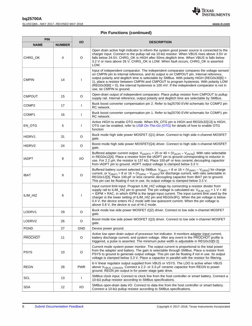
Pin Functions (continued)PIN
I/O DESCRIPTIONNAME NUMBER
CHRG_OK 4 O
Open drain active high indicator to inform the system good power source is connected to thecharger input. Connect to the pullup rail via 10-kΩ resistor. When VBUS rises above 3.5V orfalls below 24.5V, CHRG_OK is HIGH after 50ms deglitch time. When VBUS is falls below3.2 V or rises above 26 V, CHRG_OK is LOW. When fault occurs, CHRG_OK is assertedLOW.
CMPIN 14 I
Input of independent comparator. The independent comparator compares the voltage sensedon CMPIN pin to internal reference, and its output is on CMPOUT pin. Internal reference,output polarity and deglitch time is selectable by SMBus. With polarity HIGH (REG0x30[6] =1), place a resistor between CMPIN and CMPOUT to program hysteresis. With polarity LOW(REG0x30[6] = 0), the internal hysteresis is 100 mV. If the independent comparator is not inuse, tie CMPIN to ground.
CMPOUT 15 O Open-drain output of independent comparator. Place pullup resistor from CMPOUT to pullupsupply rail. Internal reference, output polarity and deglitch time are selectable by SMBus.
COMP2 17 I Buck boost converter compensation pin 2. Refer to bq25700 EVM schematic for COMP2 pinRC network.
COMP1 16 I Buck boost converter compensation pin 1. Refer to bq25700 EVM schematic for COMP1 pinRC network.
EN_OTG 5 IActive HIGH to enable OTG mode. When EN_OTG pin is HIGH and REG0x32[13] is HIGH,OTG can be enabled, refer to USB On-The-Go (OTG) for details of how to enable OTGfunction
HIDRV1 31 O Buck mode high side power MOSFET (Q1) driver. Connect to high side n-channel MOSFETgate.
HIDRV2 24 O Boost mode high side power MOSFET(Q4) driver. Connect to high side n-channel MOSFETgate.
IADPT 8 I/O
Buffered adapter current output. V(IADPT) = 20 or 40 × (V(ACP) – V(ACN)). With ratio selectablein REG0x12[4]. Place a resistor from the IADPT pin to ground corresponding to inductor inuse. For 2.2 µH, the resistor is 137 kΩ. Place 100-pF or less ceramic decoupling capacitorfrom IADPT pin to ground. IADPT output voltage is clamped below 3.3 V.
IBAT 9 O
Buffered battery current selected by SMBus. V(IBAT) = 8 or 16 × (V(SRP) – V(SRN)) for chargecurrent, or V(IBAT) = 8 or 16 × (V(SRN) – V(SRP)) for discharge current, with ratio selectable inREG0x12[3]. Place 100-pF or less ceramic decoupling capacitor from IBAT pin to ground.This pin can be floating if not in use. Its output voltage is clamped below 3.3 V.
ILIM_HIZ 6 I
Input current limit input. Program ILIM_HIZ voltage by connecting a resistor divider fromsupply rail to ILIM_HIZ pin to ground. The pin voltage is calculated as: V(ILIM_HIZ) = 1 V + 40× IDPM × RAC, in which IDPM is the target input current. The input current limit used by thecharger is the lower setting of ILIM_HIZ pin and REG0x3F(). When the pin voltage is below0.4 V, the device enters Hi-Z mode with low quiescent current. When the pin voltage isabove 0.8 V, the device is out of Hi-Z mode.
LODRV1 29 O Buck mode low side power MOSFET (Q2) driver. Connect to low side n-channel MOSFETgate.
LODRV2 26 O Boost mode low side power MOSFET (Q3) driver. Connect to low side n-channel MOSFETgate.
PGND 27 GND Device power ground.
PROCHOT 11 OActive low open drain output of processor hot indicator. It monitors adapter input current,battery discharge current, and system voltage. After any event in the PROCHOT profile istriggered, a pulse is asserted. The minimum pulse width is adjustable in REG0x33[5:2].
PSYS 10 O
Current mode system power monitor. The output current is proportional to the total powerfrom the adapter and battery. The gain is selectable through SMBus. Place a resistor fromPSYS to ground to generate output voltage. This pin can be floating if not in use. Its outputvoltage is clamped below 3.3 V. Place a capacitor in parallel with the resistor for filtering.
REGN 28 PWR6-V linear regulator output supplied from VBUS or VSYS. The LDO is active when VBUSabove VVBUS_CONVEN. Connect a 2.2- or 3.3-μF ceramic capacitor from REGN to powerground. REGN pin output is for power stage gate drive.
SCL 13 I SMBus clock input. Connect to clock line from the host controller or smart battery. Connect a10-kΩ pullup resistor according to SMBus specifications.
SDA 12 I/O SMBus open-drain data I/O. Connect to data line from the host controller or smart battery.Connect a 10-kΩ pullup resistor according to SMBus specifications.
7
bq25700Awww.ti.com SLUSCQ8A –MAY 2017–REVISED MAY 2018
Submit Documentation FeedbackCopyright © 2017–2018, Texas Instruments Incorporated
Pin Functions (continued)PIN
I/O DESCRIPTIONNAME NUMBER
SRN 19 PWR
Charge current sense resistor negative input. SRN pin is for battery voltage sensing as well.Connect SRN pin with optional 0.1-μF ceramic capacitor to GND for common-mode filtering.Connect a 0.1-μF ceramic capacitor from SRP to SRN to provide differential mode filtering.The leakage current on SRP and SRN are matched. For reverse battery plug-in protection,10-Ω series resistors are placed on SRP and SRN.
SRP 20 PWR
Charge current sense resistor positive input. Connect 0.1-μF ceramic capacitor from SRP toSRN to provide differential mode filtering. The leakage current on SRP and SRN arematched. For reverse battery plug-in protection, 10-Ω series resistors are placed on SRP andSRN. Connect SRP pin with optional 0.1-uF ceramic capacitor to GND for common-modefiltering.
SW1 32 PWR Buck mode high side power MOSFET driver source. Connect to the source of the high siden-channel MOSFET.
SW2 23 PWR Boost mode high side power MOSFET driver source. Connect to the source of the high siden-channel MOSFET.
VBUS 1 PWR Charger input voltage. An input low pass filter of 1Ω and 0.47 µF (minimum) isrecommended.
VDDA 7 PWR Internal reference bias pin. Connect a 10-Ω resistor from REGN to VDDA and a 1-μFceramic capacitor from VDDA to power ground.
VSYS 22 PWR Charger system voltage sensing. The system voltage regulation limit is programmed inREG0x15() and REG0x3E().
Thermal pad – –Exposed pad beneath the IC. Analog ground and power ground star-connected near the IC'sground. Always solder thermal pad to the board, and have vias on the thermal pad planeconnecting to power ground planes. It also serves as a thermal pad to dissipate the heat.
8
bq25700ASLUSCQ8A –MAY 2017–REVISED MAY 2018 www.ti.com
Submit Documentation Feedback Copyright © 2017–2018, Texas Instruments Incorporated
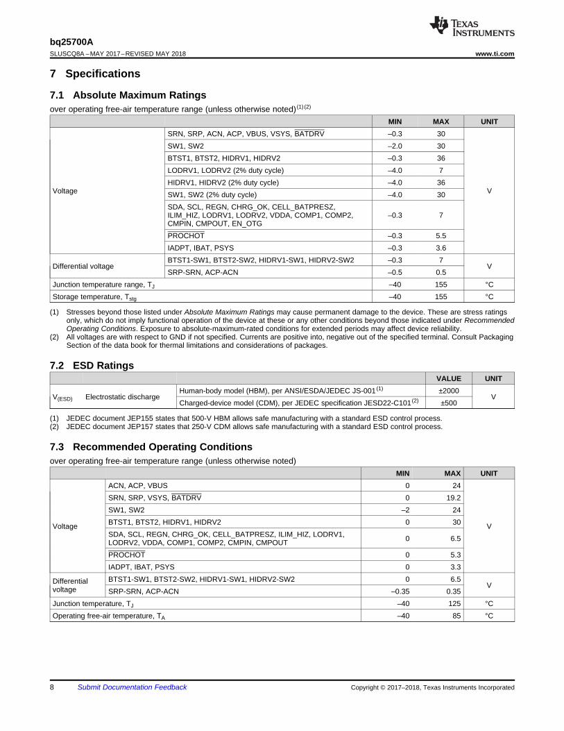
(1) Stresses beyond those listed under Absolute Maximum Ratings may cause permanent damage to the device. These are stress ratingsonly, which do not imply functional operation of the device at these or any other conditions beyond those indicated under RecommendedOperating Conditions. Exposure to absolute-maximum-rated conditions for extended periods may affect device reliability.
(2) All voltages are with respect to GND if not specified. Currents are positive into, negative out of the specified terminal. Consult PackagingSection of the data book for thermal limitations and considerations of packages.
7 Specifications
7.1 Absolute Maximum Ratingsover operating free-air temperature range (unless otherwise noted) (1) (2)
MIN MAX UNIT
Voltage
SRN, SRP, ACN, ACP, VBUS, VSYS, BATDRV –0.3 30
V
SW1, SW2 –2.0 30BTST1, BTST2, HIDRV1, HIDRV2 –0.3 36LODRV1, LODRV2 (2% duty cycle) –4.0 7HIDRV1, HIDRV2 (2% duty cycle) –4.0 36SW1, SW2 (2% duty cycle) –4.0 30SDA, SCL, REGN, CHRG_OK, CELL_BATPRESZ,ILIM_HIZ, LODRV1, LODRV2, VDDA, COMP1, COMP2,CMPIN, CMPOUT, EN_OTG
–0.3 7
PROCHOT –0.3 5.5IADPT, IBAT, PSYS –0.3 3.6
Differential voltageBTST1-SW1, BTST2-SW2, HIDRV1-SW1, HIDRV2-SW2 –0.3 7
VSRP-SRN, ACP-ACN –0.5 0.5
Junction temperature range, TJ –40 155 °CStorage temperature, Tstg –40 155 °C
(1) JEDEC document JEP155 states that 500-V HBM allows safe manufacturing with a standard ESD control process.(2) JEDEC document JEP157 states that 250-V CDM allows safe manufacturing with a standard ESD control process.
7.2 ESD RatingsVALUE UNIT
V(ESD) Electrostatic dischargeHuman-body model (HBM), per ANSI/ESDA/JEDEC JS-001 (1) ±2000
VCharged-device model (CDM), per JEDEC specification JESD22-C101 (2) ±500
7.3 Recommended Operating Conditionsover operating free-air temperature range (unless otherwise noted)
MIN MAX UNIT
Voltage
ACN, ACP, VBUS 0 24
V
SRN, SRP, VSYS, BATDRV 0 19.2SW1, SW2 –2 24BTST1, BTST2, HIDRV1, HIDRV2 0 30SDA, SCL, REGN, CHRG_OK, CELL_BATPRESZ, ILIM_HIZ, LODRV1,LODRV2, VDDA, COMP1, COMP2, CMPIN, CMPOUT 0 6.5
PROCHOT 0 5.3IADPT, IBAT, PSYS 0 3.3
Differentialvoltage
BTST1-SW1, BTST2-SW2, HIDRV1-SW1, HIDRV2-SW2 0 6.5V
SRP-SRN, ACP-ACN –0.35 0.35Junction temperature, TJ –40 125 °COperating free-air temperature, TA –40 85 °C
9
bq25700Awww.ti.com SLUSCQ8A –MAY 2017–REVISED MAY 2018
Submit Documentation FeedbackCopyright © 2017–2018, Texas Instruments Incorporated
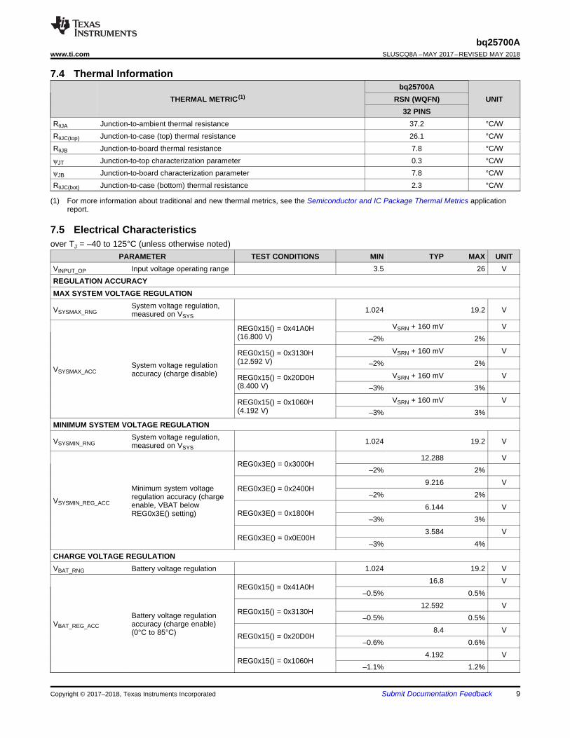
(1) For more information about traditional and new thermal metrics, see the Semiconductor and IC Package Thermal Metrics applicationreport.
7.4 Thermal Information
THERMAL METRIC (1)bq25700A
UNITRSN (WQFN)32 PINS
RθJA Junction-to-ambient thermal resistance 37.2 °C/WRθJC(top) Junction-to-case (top) thermal resistance 26.1 °C/WRθJB Junction-to-board thermal resistance 7.8 °C/WψJT Junction-to-top characterization parameter 0.3 °C/WψJB Junction-to-board characterization parameter 7.8 °C/WRθJC(bot) Junction-to-case (bottom) thermal resistance 2.3 °C/W
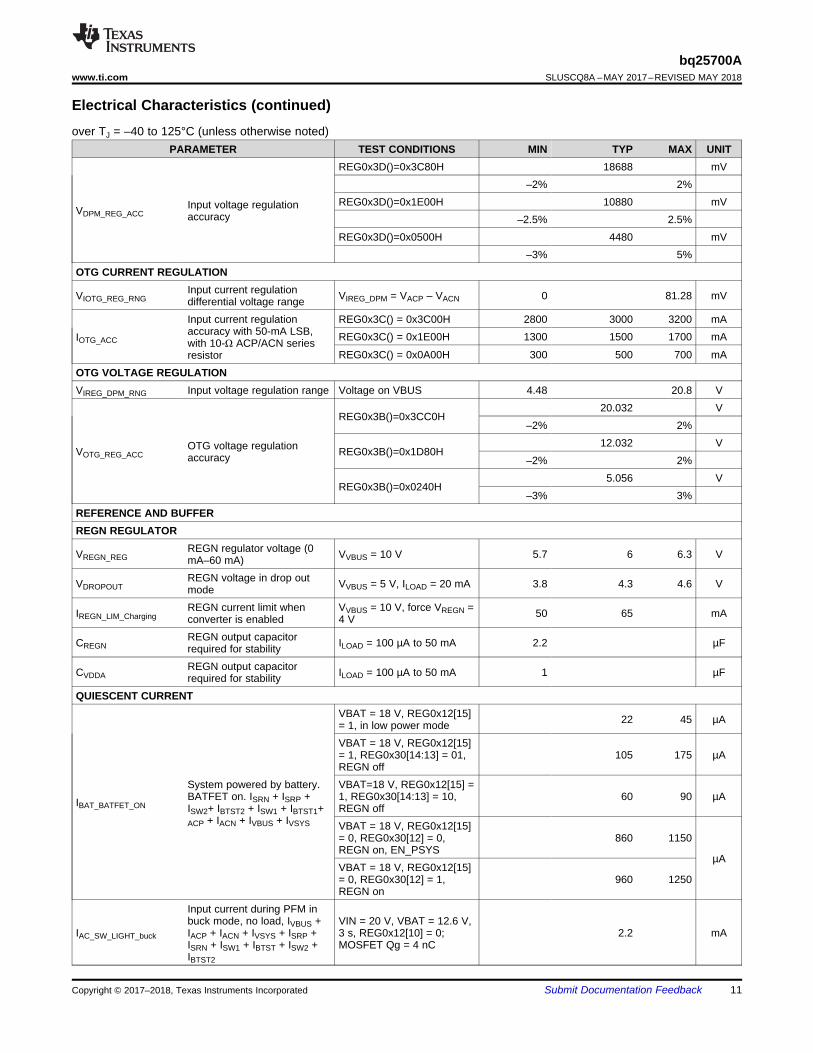
7.5 Electrical Characteristicsover TJ = –40 to 125°C (unless otherwise noted)
PARAMETER TEST CONDITIONS MIN TYP MAX UNITVINPUT_OP Input voltage operating range 3.5 26 VREGULATION ACCURACYMAX SYSTEM VOLTAGE REGULATION
VSYSMAX_RNGSystem voltage regulation,measured on VSYS
1.024 19.2 V
VSYSMAX_ACCSystem voltage regulationaccuracy (charge disable)
REG0x15() = 0x41A0H(16.800 V)
VSRN + 160 mV V–2% 2%
REG0x15() = 0x3130H(12.592 V)
VSRN + 160 mV V–2% 2%
REG0x15() = 0x20D0H(8.400 V)
VSRN + 160 mV V–3% 3%
REG0x15() = 0x1060H(4.192 V)
VSRN + 160 mV V–3% 3%
MINIMUM SYSTEM VOLTAGE REGULATION
VSYSMIN_RNGSystem voltage regulation,measured on VSYS
1.024 19.2 V
VSYSMIN_REG_ACC
Minimum system voltageregulation accuracy (chargeenable, VBAT belowREG0x3E() setting)
REG0x3E() = 0x3000H12.288 V
–2% 2%
REG0x3E() = 0x2400H9.216 V
–2% 2%
REG0x3E() = 0x1800H6.144 V
–3% 3%
REG0x3E() = 0x0E00H3.584 V
–3% 4%CHARGE VOLTAGE REGULATIONVBAT_RNG Battery voltage regulation 1.024 19.2 V
VBAT_REG_ACC
Battery voltage regulationaccuracy (charge enable)(0°C to 85°C)
REG0x15() = 0x41A0H16.8 V
–0.5% 0.5%
REG0x15() = 0x3130H12.592 V
–0.5% 0.5%
REG0x15() = 0x20D0H8.4 V
–0.6% 0.6%
REG0x15() = 0x1060H4.192 V
–1.1% 1.2%
10
bq25700ASLUSCQ8A –MAY 2017–REVISED MAY 2018 www.ti.com
Submit Documentation Feedback Copyright © 2017–2018, Texas Instruments Incorporated
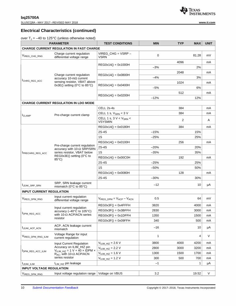
Electrical Characteristics (continued)over TJ = –40 to 125°C (unless otherwise noted)
PARAMETER TEST CONDITIONS MIN TYP MAX UNITCHARGE CURRENT REGULATION IN FAST CHARGE
VIREG_CHG_RNGCharge current regulationdifferential voltage range
VIREG_CHG = VSRP –VSRN 0 81.28 mV
ICHRG_REG_ACC
Charge current regulationaccuracy 10-mΩ currentsensing resistor, VBAT above0x3E() setting (0°C to 85°C)
REG0x14() = 0x1000H4096 mA
–3% 2%
REG0x14() = 0x0800H2048 mA
–4% 3%
REG0x14() = 0x0400H1024 mA
–5% 6%
REG0x14() = 0x0200H512 mA
–12% 12%CHARGE CURRENT REGULATION IN LDO MODE
ICLAMP Pre-charge current clamp
CELL 2s-4s 384 mACELL 1 s, VSRN < 3 V 384 mACELL 1 s, 3 V < VSRN <VSYSMIN 2 A
IPRECHRG_REG_ACC
Pre-charge current regulationaccuracy with 10-Ω SRP/SRNseries resistor, VBAT belowREG0x3E() setting (0°C to85°C)
REG0x14() = 0x0180H 384 mA2S-4S –15% 15%1S –25% 25%REG0x14() = 0x0100H 256 mA2S-4S –20% 20%1S –35% 35%REG0x14() = 0x00C0H 192 mA2S-4S –25% 25%1S –50% 50%REG0x14() = 0x0080H 128 mA2S-4S –30% 30%
ILEAK_SRP_SRNSRP, SRN leakage currentmismatch (0°C to 85°C) –12 10 µA
INPUT CURRENT REGULATION
VIREG_DPM_RNGInput current regulationdifferential voltage range VIREG_DPM = VACP – VACN 0.5 64 mV
IDPM_REG_ACC
Input current regulationaccuracy (–40°C to 105°C)with 10-Ω ACP/ACN seriesresistor
REG0x3F() = 0x4FFFH 3820 4000 mAREG0x3F() = 0x3BFFH 2830 3000 mAREG0x3F() = 0x1DFFH 1350 1500 mAREG0x3F() = 0x09FFH 340 500 mA
ILEAK_ACP_ACNACP, ACN leakage currentmismatch –16 10 µA
VIREG_DPM_RNG_ILIMVoltage Range for inputcurrent regulation 1 4 V
IDPM_REG_ACC_ILIM
Input Current RegulationAccuracy on ILIM_HIZ pinVILIM_HIZ = 1 V + 40 × IDPM ×RAC, with 10-Ω ACP/ACNseries resistor
VILIM_HIZ = 2.6 V 3800 4000 4200 mAVILIM_HIZ = 2.2 V 2800 3000 3200 mAVILIM_HIZ = 1.6 V 1300 1500 1700 mAVILIM_HIZ = 1.2 V 300 500 700 mA
ILEAK_ILIM ILIM_HIZ pin leakage –1 1 µAINPUT VOLTAGE REGULATIONVIREG_DPM_RNG Input voltage regulation range Voltage on VBUS 3.2 19.52 V
11
bq25700Awww.ti.com SLUSCQ8A –MAY 2017–REVISED MAY 2018
Submit Documentation FeedbackCopyright © 2017–2018, Texas Instruments Incorporated
Electrical Characteristics (continued)over TJ = –40 to 125°C (unless otherwise noted)
PARAMETER TEST CONDITIONS MIN TYP MAX UNIT
VDPM_REG_ACCInput voltage regulationaccuracy
REG0x3D()=0x3C80H 18688 mV–2% 2%
REG0x3D()=0x1E00H 10880 mV–2.5% 2.5%
REG0x3D()=0x0500H 4480 mV–3% 5%
OTG CURRENT REGULATION
VIOTG_REG_RNGInput current regulationdifferential voltage range VIREG_DPM = VACP – VACN 0 81.28 mV
IOTG_ACC
Input current regulationaccuracy with 50-mA LSB,with 10-Ω ACP/ACN seriesresistor
REG0x3C() = 0x3C00H 2800 3000 3200 mAREG0x3C() = 0x1E00H 1300 1500 1700 mA
REG0x3C() = 0x0A00H 300 500 700 mA
OTG VOLTAGE REGULATIONVIREG_DPM_RNG Input voltage regulation range Voltage on VBUS 4.48 20.8 V
VOTG_REG_ACCOTG voltage regulationaccuracy
REG0x3B()=0x3CC0H20.032 V
–2% 2%
REG0x3B()=0x1D80H12.032 V
–2% 2%
REG0x3B()=0x0240H5.056 V
–3% 3%REFERENCE AND BUFFERREGN REGULATOR
VREGN_REGREGN regulator voltage (0mA–60 mA) VVBUS = 10 V 5.7 6 6.3 V
VDROPOUTREGN voltage in drop outmode VVBUS = 5 V, ILOAD = 20 mA 3.8 4.3 4.6 V
IREGN_LIM_ChargingREGN current limit whenconverter is enabled
VVBUS = 10 V, force VREGN =4 V 50 65 mA
CREGNREGN output capacitorrequired for stability ILOAD = 100 µA to 50 mA 2.2 µF
CVDDAREGN output capacitorrequired for stability ILOAD = 100 µA to 50 mA 1 µF
QUIESCENT CURRENT
IBAT_BATFET_ON
System powered by battery.BATFET on. ISRN + ISRP +ISW2+ IBTST2 + ISW1 + IBTST1+ACP + IACN + IVBUS + IVSYS
VBAT = 18 V, REG0x12[15]= 1, in low power mode 22 45 µA
VBAT = 18 V, REG0x12[15]= 1, REG0x30[14:13] = 01,REGN off
105 175 µA
VBAT=18 V, REG0x12[15] =1, REG0x30[14:13] = 10,REGN off
60 90 µA
VBAT = 18 V, REG0x12[15]= 0, REG0x30[12] = 0,REGN on, EN_PSYS
860 1150
µAVBAT = 18 V, REG0x12[15]= 0, REG0x30[12] = 1,REGN on
960 1250
IAC_SW_LIGHT_buck
Input current during PFM inbuck mode, no load, IVBUS +IACP + IACN + IVSYS + ISRP +ISRN + ISW1 + IBTST + ISW2 +IBTST2
VIN = 20 V, VBAT = 12.6 V,3 s, REG0x12[10] = 0;MOSFET Qg = 4 nC
2.2 mA
12
bq25700ASLUSCQ8A –MAY 2017–REVISED MAY 2018 www.ti.com
Submit Documentation Feedback Copyright © 2017–2018, Texas Instruments Incorporated
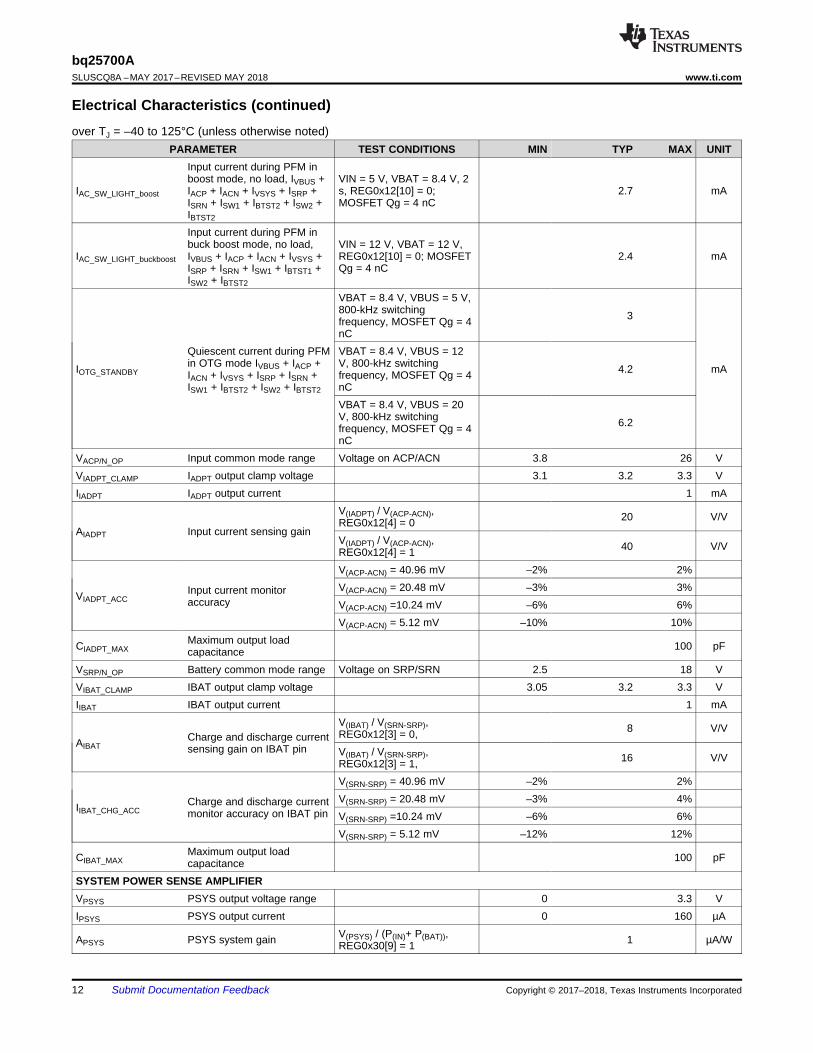
Electrical Characteristics (continued)over TJ = –40 to 125°C (unless otherwise noted)
PARAMETER TEST CONDITIONS MIN TYP MAX UNIT
IAC_SW_LIGHT_boost
Input current during PFM inboost mode, no load, IVBUS +IACP + IACN + IVSYS + ISRP +ISRN + ISW1 + IBTST2 + ISW2 +IBTST2
VIN = 5 V, VBAT = 8.4 V, 2s, REG0x12[10] = 0;MOSFET Qg = 4 nC
2.7 mA
IAC_SW_LIGHT_buckboost
Input current during PFM inbuck boost mode, no load,IVBUS + IACP + IACN + IVSYS +ISRP + ISRN + ISW1 + IBTST1 +ISW2 + IBTST2
VIN = 12 V, VBAT = 12 V,REG0x12[10] = 0; MOSFETQg = 4 nC
2.4 mA
IOTG_STANDBY
Quiescent current during PFMin OTG mode IVBUS + IACP +IACN + IVSYS + ISRP + ISRN +ISW1 + IBTST2 + ISW2 + IBTST2
VBAT = 8.4 V, VBUS = 5 V,800-kHz switchingfrequency, MOSFET Qg = 4nC
3
mA
VBAT = 8.4 V, VBUS = 12V, 800-kHz switchingfrequency, MOSFET Qg = 4nC
4.2
VBAT = 8.4 V, VBUS = 20V, 800-kHz switchingfrequency, MOSFET Qg = 4nC
6.2
VACP/N_OP Input common mode range Voltage on ACP/ACN 3.8 26 VVIADPT_CLAMP IADPT output clamp voltage 3.1 3.2 3.3 VIIADPT IADPT output current 1 mA
AIADPT Input current sensing gain
V(IADPT) / V(ACP-ACN),REG0x12[4] = 0 20 V/V
V(IADPT) / V(ACP-ACN),REG0x12[4] = 1 40 V/V
VIADPT_ACCInput current monitoraccuracy
V(ACP-ACN) = 40.96 mV –2% 2%V(ACP-ACN) = 20.48 mV –3% 3%V(ACP-ACN) =10.24 mV –6% 6%V(ACP-ACN) = 5.12 mV –10% 10%
CIADPT_MAXMaximum output loadcapacitance 100 pF
VSRP/N_OP Battery common mode range Voltage on SRP/SRN 2.5 18 VVIBAT_CLAMP IBAT output clamp voltage 3.05 3.2 3.3 VIIBAT IBAT output current 1 mA
AIBATCharge and discharge currentsensing gain on IBAT pin
V(IBAT) / V(SRN-SRP),REG0x12[3] = 0, 8 V/V
V(IBAT) / V(SRN-SRP),REG0x12[3] = 1, 16 V/V
IIBAT_CHG_ACCCharge and discharge currentmonitor accuracy on IBAT pin
V(SRN-SRP) = 40.96 mV –2% 2%V(SRN-SRP) = 20.48 mV –3% 4%V(SRN-SRP) =10.24 mV –6% 6%V(SRN-SRP) = 5.12 mV –12% 12%
CIBAT_MAXMaximum output loadcapacitance 100 pF
SYSTEM POWER SENSE AMPLIFIERVPSYS PSYS output voltage range 0 3.3 VIPSYS PSYS output current 0 160 µA
APSYS PSYS system gain V(PSYS) / (P(IN)+ P(BAT)),REG0x30[9] = 1 1 µA/W
13
bq25700Awww.ti.com SLUSCQ8A –MAY 2017–REVISED MAY 2018
Submit Documentation FeedbackCopyright © 2017–2018, Texas Instruments Incorporated
Electrical Characteristics (continued)over TJ = –40 to 125°C (unless otherwise noted)
PARAMETER TEST CONDITIONS MIN TYP MAX UNIT
VPSYS_ACCPSYS gain accuracy(REG0x30[9] = 1)
Adapter only with systempower = 19.5 V / 45 W, TA =0 to 85°C
–5% 5%
Adapter only with systempower = 19.5 V / 45 W, TA =–40 to 125°C
–7% 6%
Battery only with systempower = 11 V / 44 W, TA = 0to 85°C
–5% 5%
Battery only with systempower = 11 V / 44 W, TA =–40 to 125°C
–6% 6%
VPSYS_CLAMP PSYS clamp voltage 3 3.3 VCOMPARATORVBUS UNDER VOLTAGE LOCKOUT COMPARATOR
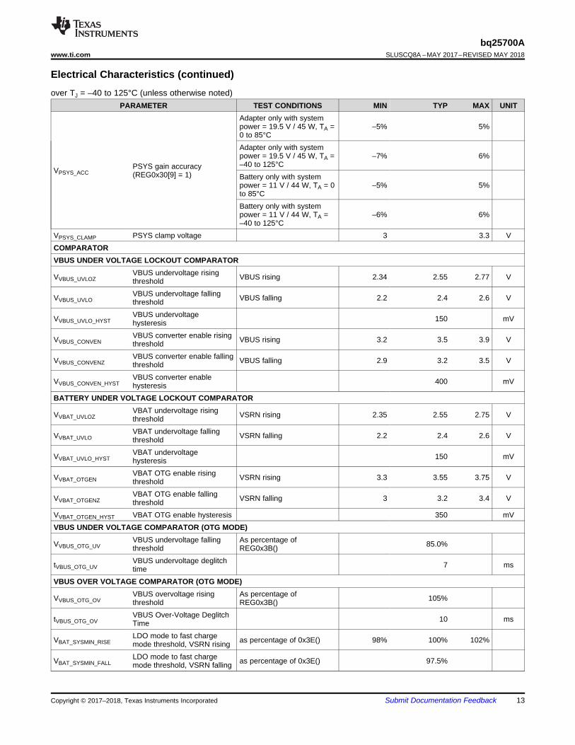
VVBUS_UVLOZVBUS undervoltage risingthreshold VBUS rising 2.34 2.55 2.77 V
VVBUS_UVLOVBUS undervoltage fallingthreshold VBUS falling 2.2 2.4 2.6 V
VVBUS_UVLO_HYSTVBUS undervoltagehysteresis 150 mV
VVBUS_CONVENVBUS converter enable risingthreshold VBUS rising 3.2 3.5 3.9 V
VVBUS_CONVENZVBUS converter enable fallingthreshold VBUS falling 2.9 3.2 3.5 V
VVBUS_CONVEN_HYSTVBUS converter enablehysteresis 400 mV
BATTERY UNDER VOLTAGE LOCKOUT COMPARATOR
VVBAT_UVLOZVBAT undervoltage risingthreshold VSRN rising 2.35 2.55 2.75 V
VVBAT_UVLOVBAT undervoltage fallingthreshold VSRN falling 2.2 2.4 2.6 V
VVBAT_UVLO_HYSTVBAT undervoltagehysteresis 150 mV
VVBAT_OTGENVBAT OTG enable risingthreshold VSRN rising 3.3 3.55 3.75 V
VVBAT_OTGENZVBAT OTG enable fallingthreshold VSRN falling 3 3.2 3.4 V
VVBAT_OTGEN_HYST VBAT OTG enable hysteresis 350 mVVBUS UNDER VOLTAGE COMPARATOR (OTG MODE)
VVBUS_OTG_UVVBUS undervoltage fallingthreshold
As percentage ofREG0x3B() 85.0%
tVBUS_OTG_UVVBUS undervoltage deglitchtime 7 ms
VBUS OVER VOLTAGE COMPARATOR (OTG MODE)
VVBUS_OTG_OVVBUS overvoltage risingthreshold
As percentage ofREG0x3B() 105%
tVBUS_OTG_OVVBUS Over-Voltage DeglitchTime 10 ms
VBAT_SYSMIN_RISELDO mode to fast chargemode threshold, VSRN rising as percentage of 0x3E() 98% 100% 102%
VBAT_SYSMIN_FALLLDO mode to fast chargemode threshold, VSRN falling as percentage of 0x3E() 97.5%
14
bq25700ASLUSCQ8A –MAY 2017–REVISED MAY 2018 www.ti.com
Submit Documentation Feedback Copyright © 2017–2018, Texas Instruments Incorporated
Electrical Characteristics (continued)over TJ = –40 to 125°C (unless otherwise noted)
PARAMETER TEST CONDITIONS MIN TYP MAX UNIT
VBAT_SYSMIN_HYSTFast charge mode to LDOmode threshold hysteresis as percentage of 0x3E() 2.5%
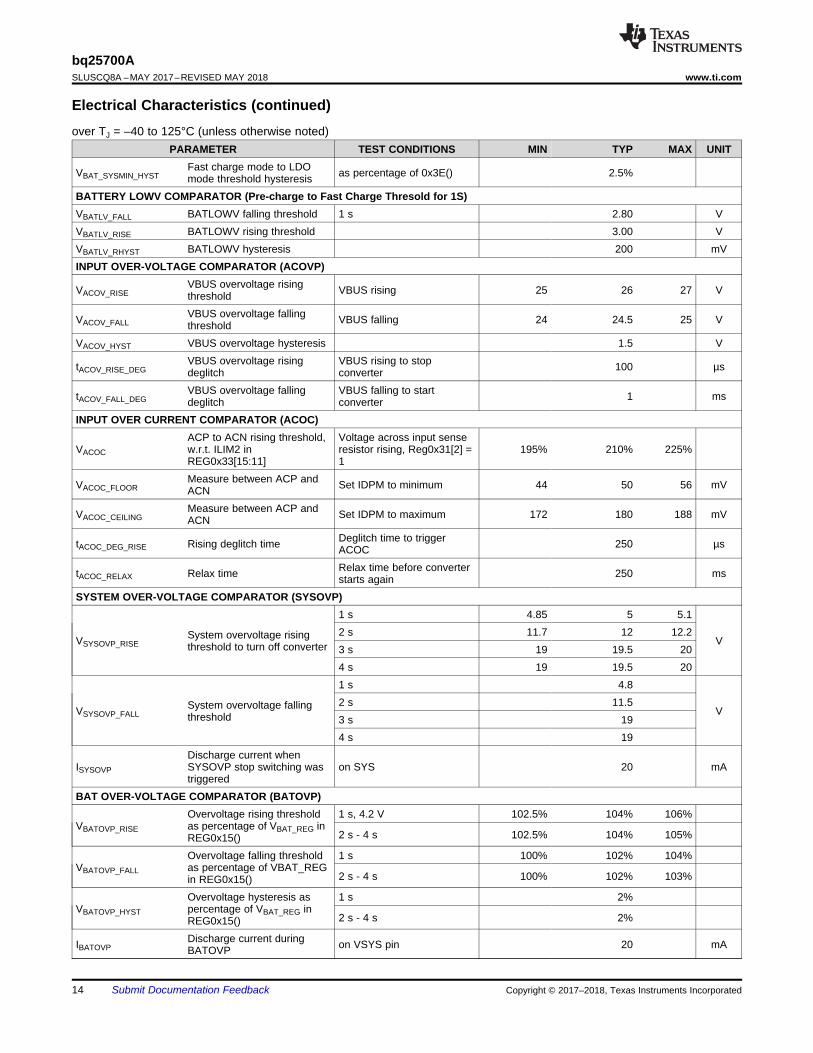
BATTERY LOWV COMPARATOR (Pre-charge to Fast Charge Thresold for 1S)VBATLV_FALL BATLOWV falling threshold 1 s 2.80 VVBATLV_RISE BATLOWV rising threshold 3.00 VVBATLV_RHYST BATLOWV hysteresis 200 mVINPUT OVER-VOLTAGE COMPARATOR (ACOVP)
VACOV_RISEVBUS overvoltage risingthreshold VBUS rising 25 26 27 V
VACOV_FALLVBUS overvoltage fallingthreshold VBUS falling 24 24.5 25 V
VACOV_HYST VBUS overvoltage hysteresis 1.5 V
tACOV_RISE_DEGVBUS overvoltage risingdeglitch
VBUS rising to stopconverter 100 µs
tACOV_FALL_DEGVBUS overvoltage fallingdeglitch
VBUS falling to startconverter 1 ms
INPUT OVER CURRENT COMPARATOR (ACOC)
VACOC
ACP to ACN rising threshold,w.r.t. ILIM2 inREG0x33[15:11]
Voltage across input senseresistor rising, Reg0x31[2] =1
195% 210% 225%
VACOC_FLOORMeasure between ACP andACN Set IDPM to minimum 44 50 56 mV
VACOC_CEILINGMeasure between ACP andACN Set IDPM to maximum 172 180 188 mV
tACOC_DEG_RISE Rising deglitch time Deglitch time to triggerACOC 250 µs
tACOC_RELAX Relax time Relax time before converterstarts again 250 ms
SYSTEM OVER-VOLTAGE COMPARATOR (SYSOVP)
VSYSOVP_RISESystem overvoltage risingthreshold to turn off converter
1 s 4.85 5 5.1
V2 s 11.7 12 12.23 s 19 19.5 204 s 19 19.5 20
VSYSOVP_FALLSystem overvoltage fallingthreshold
1 s 4.8
V2 s 11.53 s 194 s 19
ISYSOVP
Discharge current whenSYSOVP stop switching wastriggered
on SYS 20 mA
BAT OVER-VOLTAGE COMPARATOR (BATOVP)
VBATOVP_RISE
Overvoltage rising thresholdas percentage of VBAT_REG inREG0x15()
1 s, 4.2 V 102.5% 104% 106%
2 s - 4 s 102.5% 104% 105%
VBATOVP_FALL
Overvoltage falling thresholdas percentage of VBAT_REGin REG0x15()
1 s 100% 102% 104%
2 s - 4 s 100% 102% 103%
VBATOVP_HYST
Overvoltage hysteresis aspercentage of VBAT_REG inREG0x15()
1 s 2%
2 s - 4 s 2%
IBATOVPDischarge current duringBATOVP on VSYS pin 20 mA
15
bq25700Awww.ti.com SLUSCQ8A –MAY 2017–REVISED MAY 2018
Submit Documentation FeedbackCopyright © 2017–2018, Texas Instruments Incorporated
Electrical Characteristics (continued)over TJ = –40 to 125°C (unless otherwise noted)
PARAMETER TEST CONDITIONS MIN TYP MAX UNIT
tBATOVP_RISE
Overvoltage rising deglitch toturn off BATDRV to disablecharge
20 ms
CONVERTER OVER-CURRENT COMPARATOR (Q2)
VOCP_limit_Q2 Converter Over-Current LimitReg0x31[5]=1 150
mVReg0x31[5]=0 210
VOCP_limit_SYSSHORT_Q2 System Short or SRN<2.5 V
Reg0x31[5]=1 45mV
Reg0x31[5]=0 60CONVERTER OVER-CURRENT COMPARATOR (ACX)
VOCP_limit_ACX Converter Over-Current LimitReg0x31[4]=1 150
mVReg0x31[4]=0 280
VOCP_limit_SYSSHORT_ACX System Short or SRN<2.5 V
Reg0x31[4]=1 90mV
Reg0x31[4]=0 150THERMAL SHUTDOWN COMPARATOR
TSHUT_RISEThermal shutdown risingtemperature Temperature increasing 155 °C
TSHUTF_FALLThermal shutdown fallingtemperature Temperature reducing 135 °C
TSHUT_HYS Thermal shutdown hysteresis 20 °C
tSHUT_RDEGThermal shutdown risingdeglitch 100 µs
tSHUT_FHYSThermal shutdown fallingdeglitch 12 ms
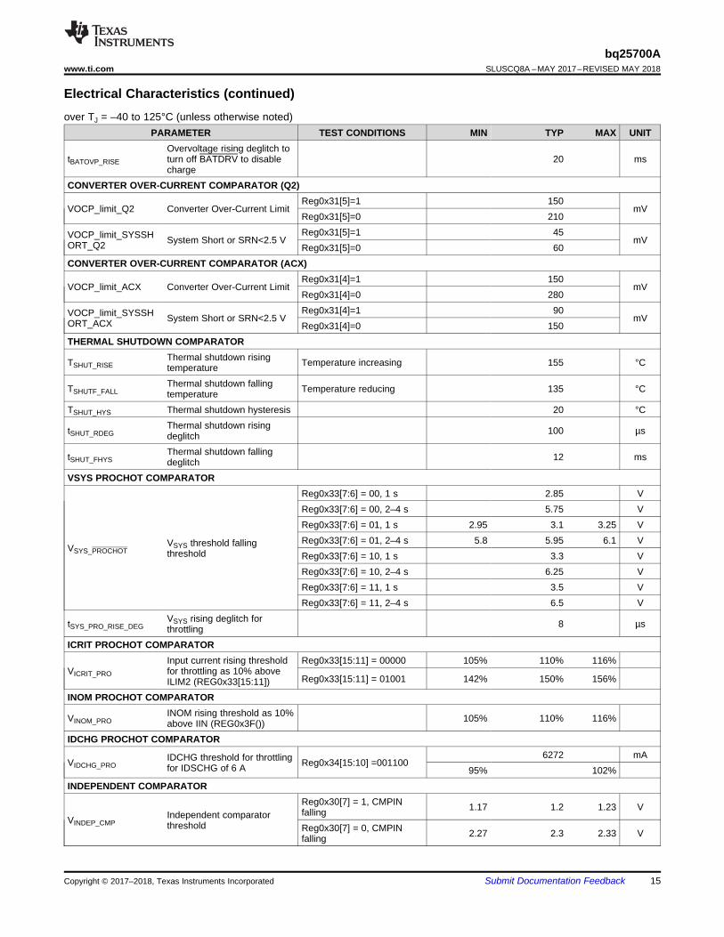
VSYS PROCHOT COMPARATOR
VSYS_PROCHOTVSYS threshold fallingthreshold
Reg0x33[7:6] = 00, 1 s 2.85 VReg0x33[7:6] = 00, 2–4 s 5.75 VReg0x33[7:6] = 01, 1 s 2.95 3.1 3.25 VReg0x33[7:6] = 01, 2–4 s 5.8 5.95 6.1 VReg0x33[7:6] = 10, 1 s 3.3 VReg0x33[7:6] = 10, 2–4 s 6.25 VReg0x33[7:6] = 11, 1 s 3.5 VReg0x33[7:6] = 11, 2–4 s 6.5 V
tSYS_PRO_RISE_DEGVSYS rising deglitch forthrottling 8 µs
ICRIT PROCHOT COMPARATOR
VICRIT_PRO
Input current rising thresholdfor throttling as 10% aboveILIM2 (REG0x33[15:11])
Reg0x33[15:11] = 00000 105% 110% 116%
Reg0x33[15:11] = 01001 142% 150% 156%
INOM PROCHOT COMPARATOR
VINOM_PROINOM rising threshold as 10%above IIN (REG0x3F()) 105% 110% 116%
IDCHG PROCHOT COMPARATOR
VIDCHG_PROIDCHG threshold for throttlingfor IDSCHG of 6 A Reg0x34[15:10] =001100
6272 mA95% 102%
INDEPENDENT COMPARATOR
VINDEP_CMPIndependent comparatorthreshold
Reg0x30[7] = 1, CMPINfalling 1.17 1.2 1.23 V
Reg0x30[7] = 0, CMPINfalling 2.27 2.3 2.33 V
16
bq25700ASLUSCQ8A –MAY 2017–REVISED MAY 2018 www.ti.com
Submit Documentation Feedback Copyright © 2017–2018, Texas Instruments Incorporated
Electrical Characteristics (continued)over TJ = –40 to 125°C (unless otherwise noted)
PARAMETER TEST CONDITIONS MIN TYP MAX UNIT
VINDEP_CMP_HYSIndependent comparatorhysteresis
Reg0x3B[6] = 0, CMPINfalling 100 mV
POWER MOSFET DRIVERPWM OSCILLATOR AND RAMP
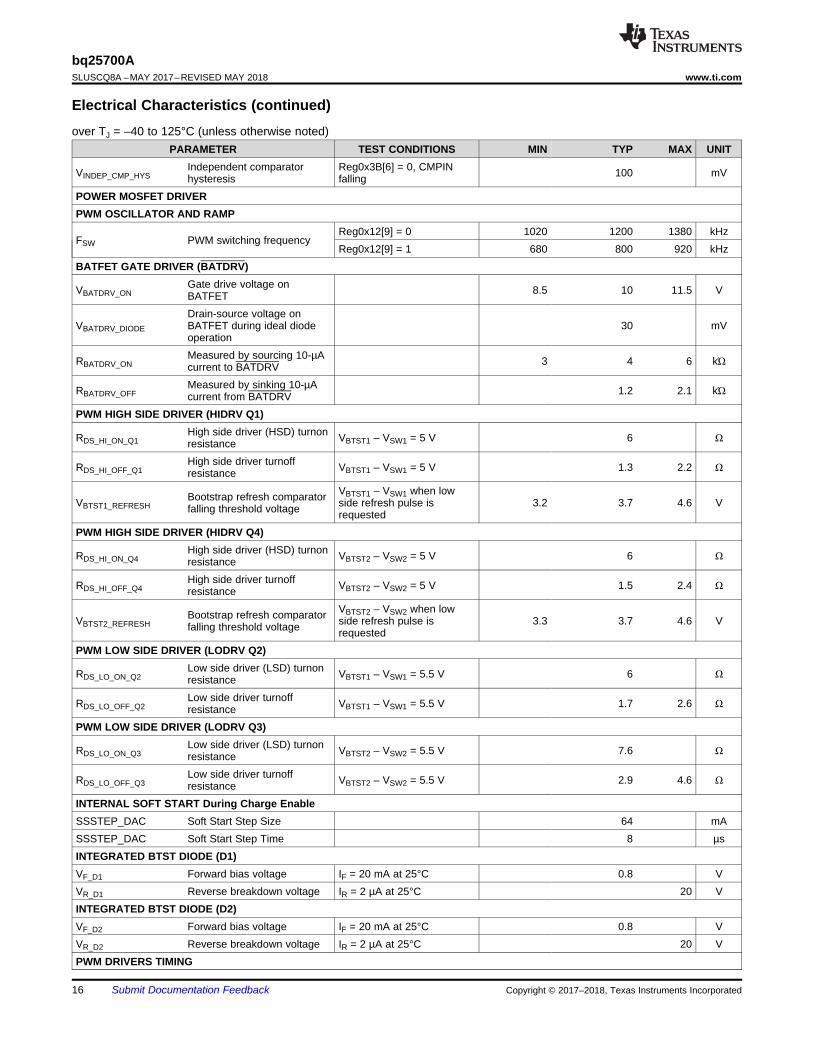
FSW PWM switching frequencyReg0x12[9] = 0 1020 1200 1380 kHzReg0x12[9] = 1 680 800 920 kHz
BATFET GATE DRIVER (BATDRV)
VBATDRV_ONGate drive voltage onBATFET 8.5 10 11.5 V
VBATDRV_DIODE
Drain-source voltage onBATFET during ideal diodeoperation
30 mV
RBATDRV_ONMeasured by sourcing 10-µAcurrent to BATDRV 3 4 6 kΏ
RBATDRV_OFFMeasured by sinking 10-µAcurrent from BATDRV 1.2 2.1 kΏ
PWM HIGH SIDE DRIVER (HIDRV Q1)
RDS_HI_ON_Q1High side driver (HSD) turnonresistance VBTST1 – VSW1 = 5 V 6 Ω
RDS_HI_OFF_Q1High side driver turnoffresistance VBTST1 – VSW1 = 5 V 1.3 2.2 Ω
VBTST1_REFRESHBootstrap refresh comparatorfalling threshold voltage
VBTST1 – VSW1 when lowside refresh pulse isrequested
3.2 3.7 4.6 V
PWM HIGH SIDE DRIVER (HIDRV Q4)
RDS_HI_ON_Q4High side driver (HSD) turnonresistance VBTST2 – VSW2 = 5 V 6 Ω
RDS_HI_OFF_Q4High side driver turnoffresistance VBTST2 – VSW2 = 5 V 1.5 2.4 Ω
VBTST2_REFRESHBootstrap refresh comparatorfalling threshold voltage
VBTST2 – VSW2 when lowside refresh pulse isrequested
3.3 3.7 4.6 V
PWM LOW SIDE DRIVER (LODRV Q2)
RDS_LO_ON_Q2Low side driver (LSD) turnonresistance VBTST1 – VSW1 = 5.5 V 6 Ω
RDS_LO_OFF_Q2Low side driver turnoffresistance VBTST1 – VSW1 = 5.5 V 1.7 2.6 Ω
PWM LOW SIDE DRIVER (LODRV Q3)
RDS_LO_ON_Q3Low side driver (LSD) turnonresistance VBTST2 – VSW2 = 5.5 V 7.6 Ω
RDS_LO_OFF_Q3Low side driver turnoffresistance VBTST2 – VSW2 = 5.5 V 2.9 4.6 Ω
INTERNAL SOFT START During Charge EnableSSSTEP_DAC Soft Start Step Size 64 mASSSTEP_DAC Soft Start Step Time 8 µsINTEGRATED BTST DIODE (D1)VF_D1 Forward bias voltage IF = 20 mA at 25°C 0.8 VVR_D1 Reverse breakdown voltage IR = 2 µA at 25°C 20 VINTEGRATED BTST DIODE (D2)VF_D2 Forward bias voltage IF = 20 mA at 25°C 0.8 VVR_D2 Reverse breakdown voltage IR = 2 µA at 25°C 20 VPWM DRIVERS TIMING
17
bq25700Awww.ti.com SLUSCQ8A –MAY 2017–REVISED MAY 2018
Submit Documentation FeedbackCopyright © 2017–2018, Texas Instruments Incorporated
Electrical Characteristics (continued)over TJ = –40 to 125°C (unless otherwise noted)
PARAMETER TEST CONDITIONS MIN TYP MAX UNITINTERFACELOGIC INPUT (SDA, SCL, EN_OTG)VIN_ LO Input low threshold SMBus 0.8 VVIN_ HI Input high threshold SMBus (bq25700A) 2.1 VLOGIC OUTPUT OPEN DRAIN (SDA, CHRG_OK, CMPOUT)VOUT_ LO Output saturation voltage 5-mA drain current 0.4 VVOUT_ LEAK Leakage current V = 7 V –1 1 mALOGIC OUTPUT OPEN DRAIN SDAVOUT_ LO_SDA Output Saturation Voltage 5 mA drain current 0.4 VVOUT_ LEAK_SDA Leakage Current V = 7V –1 1 mALOGIC OUTPUT OPEN DRAIN CHRG_OKVOUT_ LO_CHRG_OK Output Saturation Voltage 5 mA drain current 0.4 VVOUT_ LEAK _CHRG_OK Leakage Current V = 7V –1 1 mALOGIC OUTPUT OPEN DRAIN CMPOUTVOUT_ LO_CMPOUT Output Saturation Voltage 5 mA drain current 0.4 VVOUT_ LEAK _CMPOUT Leakage Current V = 7V –1 1 mALOGIC OUTPUT OPEN DRAIN (PROCHOT)
VOUT_ LO_PROCHOT Output saturation voltage 50-Ω pullup to 1.05 V / 5-mAload 300 mV
VOUT_ LEAK_PROCHOT Leakage current V = 5.5 V –1 1 mAANALOG INPUT (ILIM_HIZ)
VHIZ_ LOVoltage to get out of HIZmode ILIM_HIZ pin rising 0.8 V
VHIZ_ HIGH Voltage to enable HIZ mode ILIM_HIZ pin falling 0.4 VANALOG INPUT (CELL_BATPRESZ)
VCELL_4S 4S REGN = 6 V, as percentageof REGN 68.4% 75%
VCELL_3S 3S REGN = 6 V, as percentageof REGN 51.7% 55% 65%
VCELL_2S 2S REGN = 6 V, as percentageof REGN 35% 40% 49.1%
VCELL_1S 1S REGN = 6 V, as percentageof REGN 18.4% 25% 31.6%
VCELL_BATPRESZ_RISE Battery is present 18%VCELL_BATPRESZ_FALL Battery is removed CELL_BATPRESZ falling 15%ANALOG INPUT (COMP1, COMP2)ILEAK_COMP1 COMP1 Leakage –120 120 nAILEAK_COMP2 COMP2 Leakage –120 120 nA
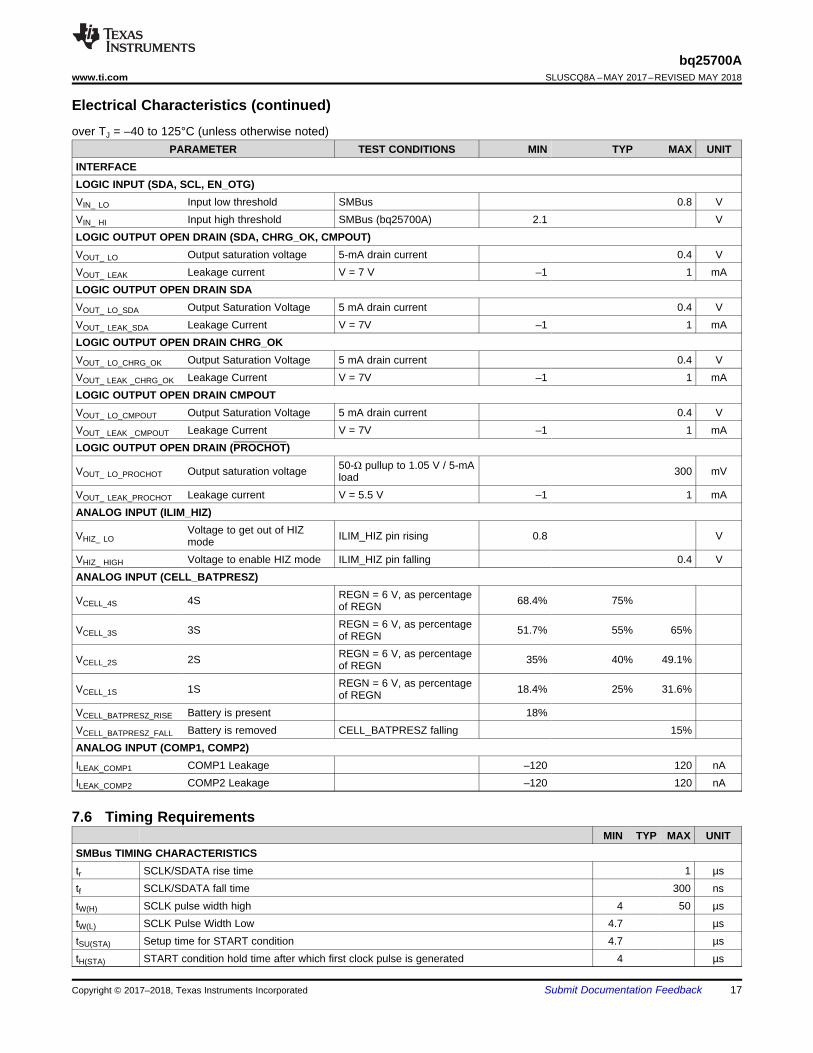
7.6 Timing RequirementsMIN TYP MAX UNIT
SMBus TIMING CHARACTERISTICStr SCLK/SDATA rise time 1 µstf SCLK/SDATA fall time 300 nstW(H) SCLK pulse width high 4 50 µstW(L) SCLK Pulse Width Low 4.7 µstSU(STA) Setup time for START condition 4.7 µstH(STA) START condition hold time after which first clock pulse is generated 4 µs
Output Current (A)
Effi
cien
cy (
%)
0 0.01 0.02 0.03 0.04 0.0560
65
70
75
80
85
90
D001
VOUT = 6.1 VVOUT = 8.4 VVOUT = 9.2 VVOUT = 12.5 V
Output Current (A)
Effi
cien
cy (
%)
0 1 2 3 4 5 680
82
84
86
88
90
92
94
96
D001
VOUT = 3.7 VVOUT = 7.4 VVOUT = 11.1 VVOUT = 14.8 V
Output Current (A)
Effi
cien
cy (
%)
0 0.01 0.02 0.03 0.04 0.0560
65
70
75
80
85
90
D001
VOUT = 6.1 VVOUT = 8.4 VVOUT = 9.2 VVOUT = 12.5 V
Output Current (A)
Effi
cien
cy (
%)
0 0.01 0.02 0.03 0.04 0.0560
65
70
75
80
85
90
D001
VOUT = 6.1 VVOUT = 8.4 VVOUT = 9.2 VVOUT = 12.5 V
18
bq25700ASLUSCQ8A –MAY 2017–REVISED MAY 2018 www.ti.com
Submit Documentation Feedback Copyright © 2017–2018, Texas Instruments Incorporated
Timing Requirements (continued)MIN TYP MAX UNIT
(1) Devices participating in a transfer will timeout when any clock low exceeds the 25ms minimum timeout period. Devices that havedetected a timeout condition must reset the communication no later than the 35 ms maximum timeout period. Both a master and a slavemust adhere to the maximum value specified as it incorporates the cumulative stretch limit for both a master (10 ms) and a slave (25ms).
(2) User can adjust threshold via SMBus ChargeOption() REG0x12.
tSU(DAT) Data setup time 250 nstH(DTA) Data hold time 300 nstSU(STOP) Setup time for STOP condition 4 µst(BUF) Bus free time between START and STOP condition 4.7 µsFS(CL) Clock Frequency 10 100 KHzHOST COMMUNICATION FAILUREttimeout SMBus bus release timeout (1) 25 35 mstBOOT Deglitch for watchdog reset signal 10 ms
tWDI
Watchdog timeout period, ChargeOption() bit [14:13] = 01 (2) 35 44 53 sWatchdog timeout period, ChargeOption() bit bit [14:13] = 10 (2) 70 88 105 sWatchdog timeout period, ChargeOption() bit bit [14:13] = 11 (2) (default) 140 175 210 s
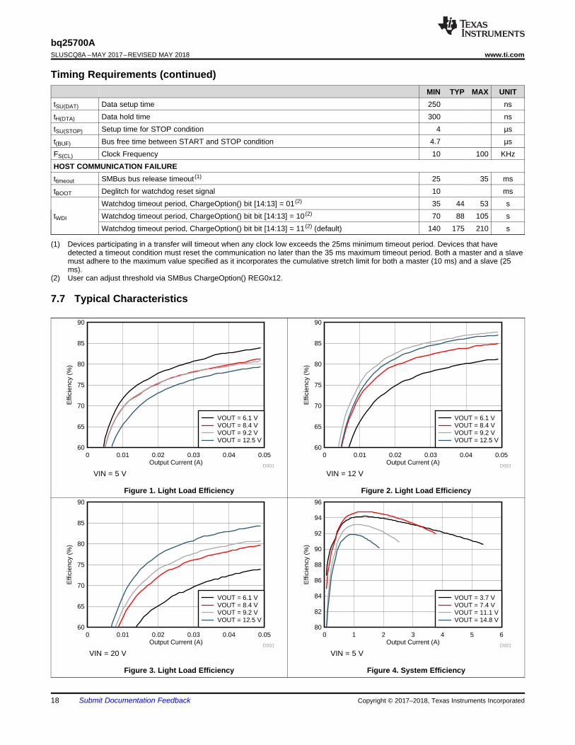
7.7 Typical Characteristics
VIN = 5 V
Figure 1. Light Load Efficiency
VIN = 12 V
Figure 2. Light Load Efficiency
VIN = 20 V
Figure 3. Light Load Efficiency
VIN = 5 V
Figure 4. System Efficiency
Output Current (A)
Effi
cien
cy (
%)
0 1 2 3 4 5 680
82
84
86
88
90
92
94
96
D001
VOTG = 5 VVOTG = 12 VVOTG = 20 V
Output Current (A)
Effi
cien
cy (
%)
0 1 2 3 4 5 680
82
84
86
88
90
92
94
96
98
D001
VOTG = 5 VVOTG = 12 VVOTG = 20 V
Output Current (A)
Effi
cien
cy (
%)
0 1 2 3 4 5 680
82
84
86
88
90
92
94
96
98
D001
VOUT = 3.7 VVOUT = 7.4 VVOUT = 11.1 VVOUT = 14.8 V
Output Current (A)
Effi
cien
cy (
%)
0 1 2 3 4 580
82
84
86
88
90
92
94
96
D001
VOTG = 5 VVOTG = 12 VVOTG = 20 V
Output Current (A)
Effi
cien
cy (
%)
0 1 2 3 4 5 680
82
84
86
88
90
92
94
96
98
D001
VOUT = 3.7 VVOUT = 7.4 VVOUT = 11.1 VVOUT = 14.8 V
Output Current (A)
Effi
cien
cy (
%)
0 1 2 3 4 5 680
82
84
86
88
90
92
94
96
98
D001
VOUT = 3.7 VVOUT = 7.4 VVOUT = 11.1 VVOUT = 14.8 V
19
bq25700Awww.ti.com SLUSCQ8A –MAY 2017–REVISED MAY 2018
Submit Documentation FeedbackCopyright © 2017–2018, Texas Instruments Incorporated
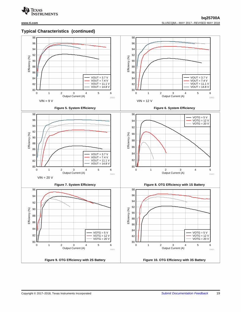
Typical Characteristics (continued)
VIN = 9 V
Figure 5. System Efficiency
VIN = 12 V
Figure 6. System Efficiency
VIN = 20 V
Figure 7. System Efficiency Figure 8. OTG Efficiency with 1S Battery
Figure 9. OTG Efficiency with 2S Battery Figure 10. OTG Efficiency with 3S Battery
Output Current (A)
Effi
cien
cy (
%)
0 1 2 3 4 5 680
82
84
86
88
90
92
94
96
98
D001
VOTG = 5 VVOTG = 12 VVOTG = 20 V
20
bq25700ASLUSCQ8A –MAY 2017–REVISED MAY 2018 www.ti.com
Submit Documentation Feedback Copyright © 2017–2018, Texas Instruments Incorporated
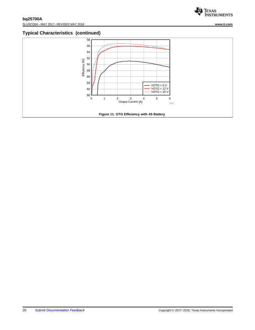
Typical Characteristics (continued)
Figure 11. OTG Efficiency with 4S Battery
21
bq25700Awww.ti.com SLUSCQ8A –MAY 2017–REVISED MAY 2018
Submit Documentation FeedbackCopyright © 2017–2018, Texas Instruments Incorporated
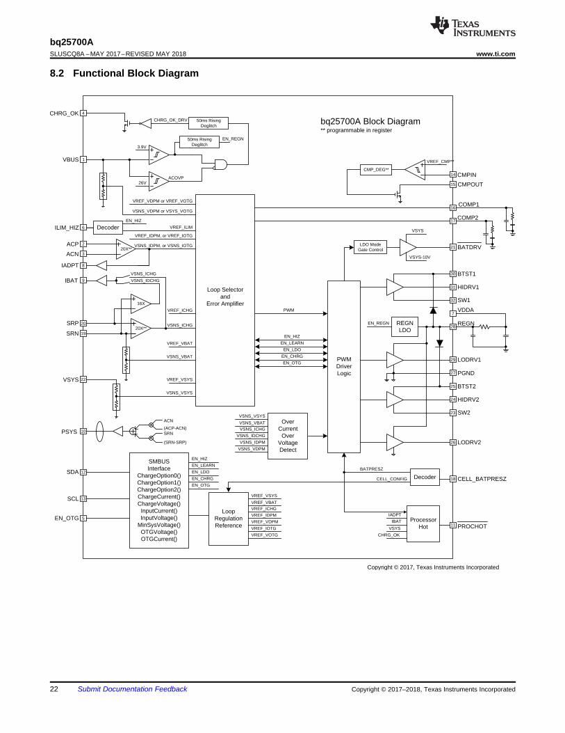
8 Detailed Description
8.1 OverviewThe bq25700A is a buck boost NVDC (narrow voltage DC) charge controller for multi-chemistry portableapplications such as notebook, detachable, ultrabook, tablet and other mobile devices with rechargeablebatteries. It provides seamless transition between converter operation modes (buck, boost, or buck boost), fasttransient response, and high light load efficiency.
The bq25700A supports wide range of power sources, including USB PD ports, legacy USB ports, traditional AC-DC adapters, etc. It takes input voltage from 3.5 V to 24 V, and charges battery of 1-4 series. It also supportsUSB On-The-Go (OTG) to provide 4.48V to 20.8V output at USB port.
The bq25700A features Dynamic Power Management (DPM) to limit the input power and avoid AC adapteroverloading. During battery charging, as the system power increases, the charging current will reduce to maintaintotal input current below adapter rating. If system power demand temporarily exceeds adapter rating, thebq25700A supports NVDC architecture to allow battery discharge energy to supplement system power. Fordetails, refer to System Voltage Regulation section.
In order to be compliant with an Intel IMVP8 compliant system, the bq25700A includes PSYS function to monitorthe total platform power from adapter and battery. Besides PSYS, it provides both an independent input currentbuffer (IADPT) and a battery current buffer (IBAT) with highly accurate current sense amplifiers. If the platformpower exceeds the available power from adapter and battery, a PROCHOT signal is asserted to CPU so that theCPU optimizes its performance to the power available to the system.
The SMBus controls input current, charge current and charge voltage registers with high resolution, highaccuracy regulation limits. It also sets the PROCHOT timing and threshold profile to meet system requirements.
50ms Rising Deglitch
20X**
20X**REGN LDO
SMBUSInterface
ChargeOption0()ChargeOption1()ChargeOption2()ChargeCurrent()ChargeVoltage()
InputCurrent()InputVoltage()
MinSysVoltage()OTGVoltage()OTGCurrent()
3.9V
ACOVP26V
CHRG_OK_DRV
VREF_IDPM, or VREF_IOTG
EN_HIZ
PWM
EN_REGN
VBUS
CHRG_OK
ACP
ACN
IADPT
SRP
SRN
SDA
SCL
PGND
LODRV1
REGN
SW1
HIDRV1
BTST1
VREF_VBAT
bq25700A Block Diagram** programmable in register
4
2
3
PWM Driver Logic
IBAT
PSYS
CELL_BATPRESZ
ProcessorHot PROCHOT
IADPT
IBAT
VSYS
ACN
(ACP-ACN)SRN
(SRN-SRP)
16X
VREF_ICHG
ILIM_HIZ
LODRV2
SW2
HIDRV2
BTST2
CMPIN
CMPOUT
VREF_CMP**
CMP_DEG**
Loop Selector and
Error Amplifier
VREF_VDPM or VREF_VOTG
VREF_ILIM
VSNS_IDPM, or VSNS_IOTG
VSNS_ICHG
VSNS_VBAT
VSYS
VSNS_VSYS
VREF_VSYS
VSNS_VDPM or VSYS_VOTG
Over Current
Over VoltageDetect
VSNS_VSYS
VSNS_VBATVSNS_ICHG
VSNS_IDCHG
VSNS_IDPM
VSNS_VDPM
VSNS_IDCHG
Loop Regulation Reference
VREF_VSYS
VREF_VBATVREF_ICHG
VREF_IDPM
VREF_VDPM
EN_LEARN
EN_LDO
EN_CHRG
EN_HIZ
EN_LEARN
EN_LDO
EN_CHRG
BATDRV
VSYS
VSYS-10V
LDO ModeGate Control
BATPRESZ
CHRG_OK
DecoderCELL_CONFIG
COMP1
COMP2
DecoderEN_HIZ
EN_OTG
EN_OTG
EN_OTG
VDDA
8
9
10
VSNS_ICHG
VREF_IOTG
VREF_VOTG
1
6
20
19
22
12
13
5
11
18
26
23
27
24
25
29
28
7
32
31
30
21
17
16
15
14
Copyright © 2017, Texas Instruments Incorporated
EN_REGN50ms Rising Deglitch
22
bq25700ASLUSCQ8A –MAY 2017–REVISED MAY 2018 www.ti.com
Submit Documentation Feedback Copyright © 2017–2018, Texas Instruments Incorporated
8.2 Functional Block Diagram
23
bq25700Awww.ti.com SLUSCQ8A –MAY 2017–REVISED MAY 2018
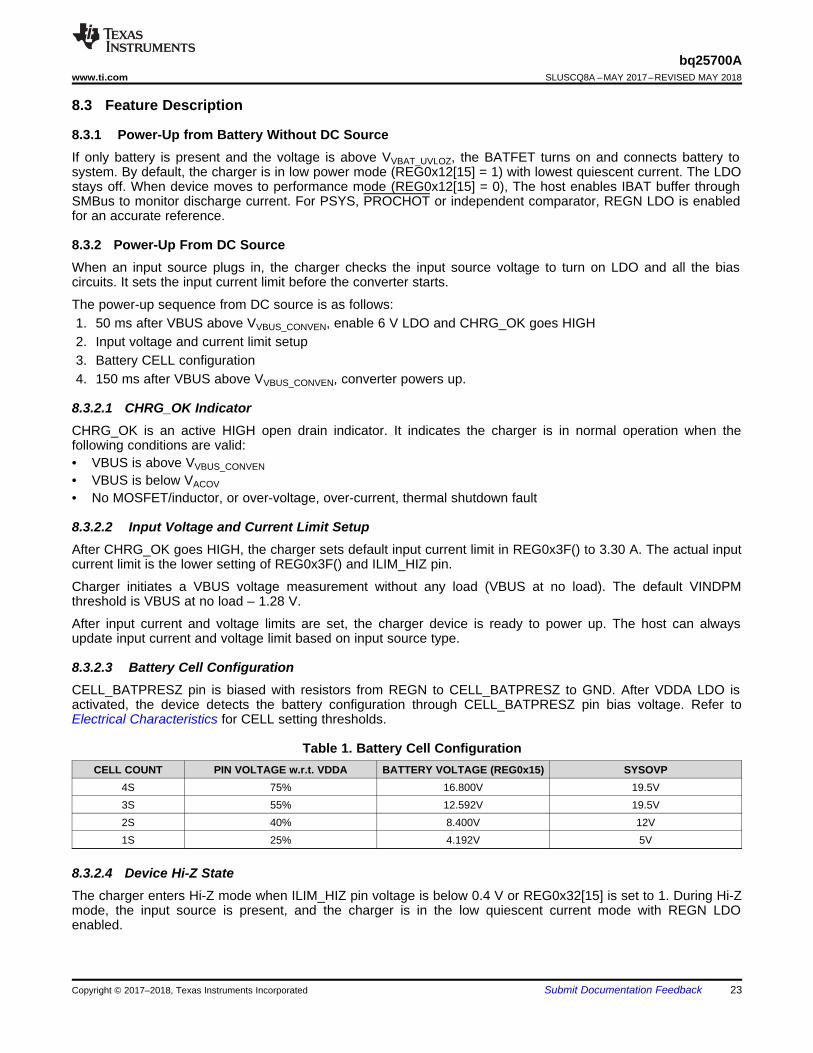
Submit Documentation FeedbackCopyright © 2017–2018, Texas Instruments Incorporated
8.3 Feature Description
8.3.1 Power-Up from Battery Without DC SourceIf only battery is present and the voltage is above VVBAT_UVLOZ, the BATFET turns on and connects battery tosystem. By default, the charger is in low power mode (REG0x12[15] = 1) with lowest quiescent current. The LDOstays off. When device moves to performance mode (REG0x12[15] = 0), The host enables IBAT buffer throughSMBus to monitor discharge current. For PSYS, PROCHOT or independent comparator, REGN LDO is enabledfor an accurate reference.
8.3.2 Power-Up From DC SourceWhen an input source plugs in, the charger checks the input source voltage to turn on LDO and all the biascircuits. It sets the input current limit before the converter starts.
The power-up sequence from DC source is as follows:1. 50 ms after VBUS above VVBUS_CONVEN, enable 6 V LDO and CHRG_OK goes HIGH2. Input voltage and current limit setup3. Battery CELL configuration4. 150 ms after VBUS above VVBUS_CONVEN, converter powers up.
8.3.2.1 CHRG_OK IndicatorCHRG_OK is an active HIGH open drain indicator. It indicates the charger is in normal operation when thefollowing conditions are valid:• VBUS is above VVBUS_CONVEN• VBUS is below VACOV• No MOSFET/inductor, or over-voltage, over-current, thermal shutdown fault
8.3.2.2 Input Voltage and Current Limit SetupAfter CHRG_OK goes HIGH, the charger sets default input current limit in REG0x3F() to 3.30 A. The actual inputcurrent limit is the lower setting of REG0x3F() and ILIM_HIZ pin.
Charger initiates a VBUS voltage measurement without any load (VBUS at no load). The default VINDPMthreshold is VBUS at no load – 1.28 V.
After input current and voltage limits are set, the charger device is ready to power up. The host can alwaysupdate input current and voltage limit based on input source type.
8.3.2.3 Battery Cell ConfigurationCELL_BATPRESZ pin is biased with resistors from REGN to CELL_BATPRESZ to GND. After VDDA LDO isactivated, the device detects the battery configuration through CELL_BATPRESZ pin bias voltage. Refer toElectrical Characteristics for CELL setting thresholds.
Table 1. Battery Cell ConfigurationCELL COUNT PIN VOLTAGE w.r.t. VDDA BATTERY VOLTAGE (REG0x15) SYSOVP
4S 75% 16.800V 19.5V3S 55% 12.592V 19.5V2S 40% 8.400V 12V1S 25% 4.192V 5V
8.3.2.4 Device Hi-Z StateThe charger enters Hi-Z mode when ILIM_HIZ pin voltage is below 0.4 V or REG0x32[15] is set to 1. During Hi-Zmode, the input source is present, and the charger is in the low quiescent current mode with REGN LDOenabled.
24
bq25700ASLUSCQ8A –MAY 2017–REVISED MAY 2018 www.ti.com
Submit Documentation Feedback Copyright © 2017–2018, Texas Instruments Incorporated
8.3.3 USB On-The-Go (OTG)The device supports USB OTG operation to deliver power from the battery to other portable devices throughUSB port. The OTG mode output voltage is set in REG0x3B(). The OTG mode output current is set inREG0x3C(). The OTG operation can be enabled if the conditions are valid:• Valid battery voltage is set REG0x15()• OTG output voltage is set in REG0x3B() and output current is set in REG0x3C()• EN_OTG pin is HIGH and REG0x32[12] = 1• VBUS is below VVBUS_UVLO• 10 ms after the above conditions are valid, converter starts and VBUS ramps up to target voltage. CHRG_OK
pin goes HIGH if REG0x12[11] = 1.
8.3.4 Converter OperationThe charger employs a synchronous buck-boost converter that allows charging from a standard 5-V or a high-voltage power source. The charger operates in buck, buck-boost and boost mode. The buck-boost can operateuninterruptedly and continuously across the three operation modes.
Table 2. MOSFET OperationMODE BUCK BUCK-BOOST BOOST
Q1 Switching Switching ONQ2 Switching Switching OFFQ3 OFF Switching SwitchingQ4 ON Switching Switching
8.3.4.1 Inductor Setting through IADPT PinThe charger reads the inductor value through the IADPT pin.
Table 3. Inductor Setting on IADPT PinINDUCTOR IN USE RESISTOR ON IADPT PIN
1 µH 93 kΩ2.2 µH 137 kΩ3.3 µH 169 kΩ
8.3.4.2 Continuous Conduction Mode (CCM)With sufficient charge current, the inductor current does not cross 0 A, which is defined as CCM. The controllerstarts a new cycle with ramp coming up from 200 mV. As long as error amplifier output voltage is above the rampvoltage, the high-side MOSFET (HSFET) stays on. When the ramp voltage exceeds error amplifier outputvoltage, HSFET turns off and low-side MOSFET (LSFET) turns on. At the end of the cycle, ramp gets reset andLSFET turns off, ready for the next cycle. There is always break-before-make logic during transition to preventcross-conduction and shoot-through. During the dead time when both MOSFETs are off, the body-diode of thelow-side power MOSFET conducts the inductor current.
During CCM, the inductor current always flows and creates a fixed two-pole system. Having the LSFET turn-onwhen the HSFET is off keeps the power dissipation low and allows safe charging at high currents.
8.3.4.3 Pulse Frequency Modulation (PFM)In order to improve converter light-load efficiency, the bq25700A switches to PFM control at light load. Theeffective switching frequency will decrease accordingly when system load decreases. The minimum frequencycan be limit to 25 kHz (ChargeOption0() bit[10]=1).
PSYS PSYS PSYS ACP IN BAT BATV R K (V I V I ) u u � u
25
bq25700Awww.ti.com SLUSCQ8A –MAY 2017–REVISED MAY 2018
Submit Documentation FeedbackCopyright © 2017–2018, Texas Instruments Incorporated
8.3.5 Current and Power Monitor
8.3.5.1 High-Accuracy Current Sense Amplifier (IADPT and IBAT)As an industry standard, a high-accuracy current sense amplifier (CSA) is used to monitor the input currentduring forward charging, or output current during OTG (IADPT) and the charge/discharge current (IBAT). IADPTvoltage is 20× or 40× the differential voltage across ACP and ACN. IBAT voltage is 8x/16× (during charging), or8×/16× (during discharging) of the differential across SRP and SRN. After input voltage or battery voltage isabove UVLO, IADPT output becomes valid. To lower the voltage on current monitoring, a resistor divider fromCSA output to GND can be used and accuracy over temperature can still be achieved.• V(IADPT) = 20 or 40 × (V(ACP) – V(ACN)) during forward mode, or 20 or 40 × (V(ACN) – V(ACP)) during reverse OTG
mode.• V(IBAT) = 8 or 16 × (V(SRP) – V(SRN)) during forward mode.• V(IBAT) = 8 or 16 × (V(SRN) – V(SRP)) during forward supplement mode, or reverse OTG mode.
A maximum 100-pF capacitor is recommended to connect on the output for decoupling high-frequency noise. Anadditional RC filter is optional, if additional filtering is desired. Note that adding filtering also adds additionalresponse delay. The CSA output voltage is clamped at 3.3 V.
8.3.5.2 High-Accuracy Power Sense Amplifier (PSYS)The charger monitors total system power. During forward mode, the input adapter powers system. Duringreverse OTG mode, the battery powers the system and VBUS output. The ratio of PSYS current and total powerKPSYS can be programmed in REG0x30[9] with default 1 μA/W. The input and charge sense resistors (RAC andRSR) are programmed in REG0x30[11:10]. PSYS voltage can be calculated with Equation 1 where IIN>0 whenadapter is in forward charging, and IBAT>0 when the battery is in discharge when the battery is in discharge.
(1)
For proper PSYS functionality, RAC and RSR values are limited to 10 mΩ and 20 mΩ.
8.3.6 Input Source Dynamic Power ManageRefer to Input Current and Input Voltage Registers for Dynamic Power Management.
8.3.7 Two-Level Adapter Current Limit (Peak Power Mode)Usually adapter can supply current higher than DC rating for a few milliseconds to tens of milliseconds. Thecharger employs two-level input current limit, or peak power mode, to fully utilize the overloading capability andminimize battery discharge during CPU turbo mode. Peak power mode is enabled inREG0x31[13](EN_PKPWR_IDPM) or REG0x31[12(EN_PKPWR_VSYS)]. The DC current limit, or ILIM1, is thesame as adapter DC current, set in REG0x3F(). The overloading current, or ILIM2, is set in REG0x33[15:11], as apercentage of ILIM1.
When the charger detects input current surge and battery discharge due to load transient, it applies ILIM2 forTOVLD in REG0x31[15:14], first, and then ILIM1 for up to TMAX – TOVLD time. TMAX is programmed in REG0x31[9:8].After TMAX, if the load is still high, another peak power cycle starts. Charging is disabled during TMAX,; once TMAX,expires, charging continues. If TOVLD is programmed higher than TMAX, then peak power mode is always on.
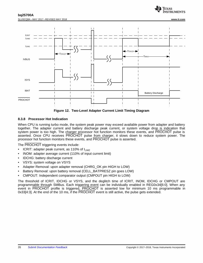
TOVLD
TMAX
TOVLD
IVBUS
PROCHOT
ILIM1
ILIM2
ICRIT
ISYS
IBATBattery Discharge
26
bq25700ASLUSCQ8A –MAY 2017–REVISED MAY 2018 www.ti.com
Submit Documentation Feedback Copyright © 2017–2018, Texas Instruments Incorporated
Figure 12. Two-Level Adapter Current Limit Timing Diagram
8.3.8 Processor Hot IndicationWhen CPU is running turbo mode, the system peak power may exceed available power from adapter and batterytogether. The adapter current and battery discharge peak current, or system voltage drop is indication thatsystem power is too high. The charger processor hot function monitors these events, and PROCHOT pulse isasserted. Once CPU receives PROCHOT pulse from charger, it slows down to reduce system power. Theprocessor hot function monitors these events, and PROCHOT pulse is asserted.
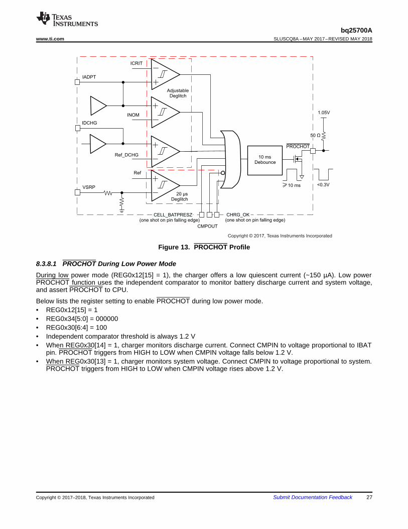
The PROCHOT triggering events include:• ICRIT: adapter peak current, as 110% of ILIM2• INOM: adapter average current (110% of input current limit)• IDCHG: battery discharge current• VSYS: system voltage on VSYS• Adapter Removal: upon adapter removal (CHRG_OK pin HIGH to LOW)• Battery Removal: upon battery removal (CELL_BATPRESZ pin goes LOW)• CMPOUT: Independent comparator output (CMPOUT pin HIGH to LOW)
The threshold of ICRIT, IDCHG or VSYS, and the deglitch time of ICRIT, INOM, IDCHG or CMPOUT areprogrammable through SMBus. Each triggering event can be individually enabled in REG0x34[6:0]. When anyevent in PROCHOT profile is triggered, PROCHOT is asserted low for minimum 10 ms programmable in0x33[4:3]. At the end of the 10 ms, if the PROCHOT event is still active, the pulse gets extended.
IADPT
IDCHG
Ref_DCHG
Ref
CMPOUT
20 µsDeglitch
10 msDebounce
VSRP
INOM
AdjustableDeglitch
PROCHOT
ICRIT
CELL_BATPRESZ(one shot on pin falling edge)
10 ms
1.05V
<0.3V
50 Ω
CHRG_OK(one shot on pin falling edge)
Copyright © 2017, Texas Instruments Incorporated
27
bq25700Awww.ti.com SLUSCQ8A –MAY 2017–REVISED MAY 2018
Submit Documentation FeedbackCopyright © 2017–2018, Texas Instruments Incorporated
Figure 13. PROCHOT Profile
8.3.8.1 PROCHOT During Low Power ModeDuring low power mode (REG0x12[15] = 1), the charger offers a low quiescent current (~150 µA). Low powerPROCHOT function uses the independent comparator to monitor battery discharge current and system voltage,and assert PROCHOT to CPU.
Below lists the register setting to enable PROCHOT during low power mode.• REG0x12[15] = 1• REG0x34[5:0] = 000000• REG0x30[6:4] = 100• Independent comparator threshold is always 1.2 V• When REG0x30[14] = 1, charger monitors discharge current. Connect CMPIN to voltage proportional to IBAT
pin. PROCHOT triggers from HIGH to LOW when CMPIN voltage falls below 1.2 V.• When REG0x30[13] = 1, charger monitors system voltage. Connect CMPIN to voltage proportional to system.
PROCHOT triggers from HIGH to LOW when CMPIN voltage rises above 1.2 V.
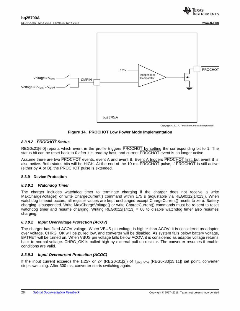
PROCHOT
IndependentComparator
1.2 V
bq2570xA
CMPINVSYSvVoltage
(VSRN ± VSRP)vVoltage
Copyright © 2017, Texas Instruments Incorporated
28
bq25700ASLUSCQ8A –MAY 2017–REVISED MAY 2018 www.ti.com
Submit Documentation Feedback Copyright © 2017–2018, Texas Instruments Incorporated
Figure 14. PROCHOT Low Power Mode Implementation
8.3.8.2 PROCHOT StatusREG0x21[6:0] reports which event in the profile triggers PROCHOT by setting the corresponding bit to 1. Thestatus bit can be reset back to 0 after it is read by host, and current PROCHOT event is no longer active.
Assume there are two PROCHOT events, event A and event B. Event A triggers PROCHOT first, but event B isalso active. Both status bits will be HIGH. At the end of the 10 ms PROCHOT pulse, if PROCHOT is still active(either by A or B), the PROCHOT pulse is extended.
8.3.9 Device Protection
8.3.9.1 Watchdog TimerThe charger includes watchdog timer to terminate charging if the charger does not receive a writeMaxChargeVoltage() or write ChargeCurrent() command within 175 s (adjustable via REG0x12[14:13]). Whenwatchdog timeout occurs, all register values are kept unchanged except ChargeCurrent() resets to zero. Batterycharging is suspended. Write MaxChargeVoltage() or write ChargeCurrent() commands must be re-sent to resetwatchdog timer and resume charging. Writing REG0x12[14:13] = 00 to disable watchdog timer also resumescharging.
8.3.9.2 Input Overvoltage Protection (ACOV)The charger has fixed ACOV voltage. When VBUS pin voltage is higher than ACOV, it is considered as adapterover voltage. CHRG_OK will be pulled low, and converter will be disabled. As system falls below battery voltage,BATFET will be turned on. When VBUS pin voltage falls below ACOV, it is considered as adapter voltage returnsback to normal voltage. CHRG_OK is pulled high by external pull up resistor. The converter resumes if enableconditions are valid.
8.3.9.3 Input Overcurrent Protection (ACOC)If the input current exceeds the 1.25× or 2× (REG0x31[2]) of ILIM2_VTH (REG0x33[15:11]) set point, converterstops switching. After 300 ms, converter starts switching again.
29
bq25700Awww.ti.com SLUSCQ8A –MAY 2017–REVISED MAY 2018
Submit Documentation FeedbackCopyright © 2017–2018, Texas Instruments Incorporated
8.3.9.4 System Overvoltage Protection (SYSOVP)When the converter starts up, the bq25700A reads CELL pin configuration and sets MaxChargeVoltage() andSYSOVP threshold (1s – 5 V, 2s – 12 V, 3s/4s – 19.5 V). Before REGx15() is written by the host, the batteryconfiguration will change with CELL pin voltage. When SYSOVP happens, the device latches off the converter.REG20[4] is set as 1. The user can clear latch-off by either writing 0 to the SYSOVP bit or removing andplugging in the adapter again. After latch-off is cleared, the converter starts again.
8.3.9.5 Battery Overvoltage Protection (BATOVP)Battery over-voltage may happen when battery is removed during charging or the user plugs in a wrong battery.The BATOVP threshold is 104% (1 s) or 102% (2 s to 4 s) of regulation voltage set in REG0x15().
8.3.9.6 Battery ShortIf BAT voltage falls below SYSMIN during charging, the maximum current is limited to 384 mA.
8.3.9.7 Thermal Shutdown (TSHUT)The WQFN package has low thermal impedance, which provides good thermal conduction from the silicon to theambient, to keep junction temperatures low. As added level of protection, the charger converter turns off for self-protection whenever the junction temperature exceeds the 155°C. The charger stays off until the junctiontemperature falls below 135°C. During thermal shut down, the LDO current limit is reduced to 16 mA and REGNLDO stays off. When the temperature falls below 135°C, charge can be resumed with soft start.
8.4 Device Functional Modes
8.4.1 Forward ModeWhen input source is connected to VBUS, bq25700A is in forward mode to regulate system and charge battery.
8.4.1.1 System Voltage Regulation with Narrow VDC ArchitectureThe bq25700A employs Narrow VDC architecture (NVDC) with BATFET separating system from battery. Theminimum system voltage is set by MinSystemVoltage(). Even with a deeply depleted battery, the system isregulated above the minimum system voltage.
When the battery is below minimum system voltage setting, the BATFET operates in linear mode (LDO mode).
As the battery voltage rises above the minimum system voltage, BATFET is fully on when charging or insupplement mode and the voltage difference between the system and battery is the VDS of BATFET. Systemvoltage is regulated 160 mV above battery voltage when BATFET is off (no charging or no supplement current).
See System Voltage Regulation for details on system voltage regulation and register programming.
8.4.1.2 Battery ChargingThe bq25700A charges 1-4 cell battery in constant current (CC), and constant voltage (CV) mode. Based onCELL_BATPREZ pin setting, the charger sets default battery voltage 4.2V/cell to ChargeVoltage(), orREG0x15(). According to battery capacity, the host programs appropriate charge current to ChargeCurrent(), orREG0x14(). When battery is full or battery is not in good condition to charge, host terminates charge by settingREG0x12[0] to 1, or setting ChargeCurrent() to zero.
See Feature Description for details on register programming.
8.4.2 USB On-The-GoThe bq25700A supports USB OTG functionality to deliver power from the battery to other portable devicesthrough USB port (reverse mode). The OTG output voltage is compliant with USB PD specification, including 5 V,9 V, 15 V, and 20 V (REG0x3B()). The output current regulation is compliant with USB type C specification,including 500 mA, 1.5 A, 3 A and 5 A (REG0x3C()).
Similar to forward operation, the device switches from PWM operation to PFM operation at light load to improveefficiency.
30
bq25700ASLUSCQ8A –MAY 2017–REVISED MAY 2018 www.ti.com
Submit Documentation Feedback Copyright © 2017–2018, Texas Instruments Incorporated
8.5 ProgrammingThe charger supports battery-charger commands that use either Write-Word or Read-Word protocols, assummarized in Table 6. The SMBUS address is 12h (0001001_X), where X is the read/write bit. TheManufacturerID and DeviceID registers are assigned identify the charger device. The ManufacturerID registercommand always returns 40h.
8.5.1 SMBus InterfaceThe bq25700A device operates as a slave, receiving control inputs from the embedded controller host throughthe SMBus interface. The bq25700A device uses a simplified subset of the commands documented in SystemManagement Bus Specification V1.1, which can be downloaded from www.smbus.org. The bq25700A deviceuses the SMBus read-word and write-word protocols (shown in Table 4 and Table 5) to communicate with thesmart battery. The device performs only as a SMBus slave device with address 0b00010010 (0x12H) and doesnot initiate communication on the bus. In addition, the device has two identification registers, a 16-bit device IDregister (0xFFH) and a 16-bit manufacturer ID register (0xFEH).
SMBus communication starts when VCC is above V(UVLO).
The data (SDA) and clock (SCL) pins have Schmitt-trigger inputs that can accommodate slow edges. Choosepullup resistors (10 kΩ) for SDA and SCL to achieve rise times according to the SMBus specifications.Communication starts when the master signals a start condition, which is a high-to-low transition on SDA, whileSCL is high. When the master has finished communicating, the master issues a stop condition, which is a low-to-high transition on SDA, while SCL is high. The bus is then free for another transmission. Figure 15 and Figure 16show the timing diagram for signals on the SMBus interface. The address byte, command byte, and data bytesare transmitted between the start and stop conditions. The SDA state changes only while SCL is low, except forthe start and stop conditions. Data is transmitted in 8-bit bytes and is sampled on the rising edge of SCL. Nineclock cycles are required to transfer each byte in or out of the device because either the master or the slaveacknowledges the receipt of the correct byte during the ninth clock cycle. The bq25700A supports the chargercommands listed in Table 4.
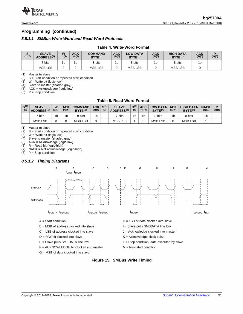
A B C D E F G H I J K L M
tLOW tHIGH
SMBCLK
SMBDATA
tSU:STA tHD:STA SU:DATt tHD:DAT HD:DATt tSU:STO tBUF
31
bq25700Awww.ti.com SLUSCQ8A –MAY 2017–REVISED MAY 2018
Submit Documentation FeedbackCopyright © 2017–2018, Texas Instruments Incorporated
Programming (continued)
(1) Master to slave(2) S = Start condition or repeated start condition(3) W = Write bit (logic-low)(4) Slave to master (shaded gray)(5) ACK = Acknowledge (logic-low)(6) P = Stop condition
8.5.1.1 SMBus Write-Word and Read-Word Protocols
Table 4. Write-Word FormatS
(1) (2)SLAVE
ADDRESS (1)W
(1) (3)ACK(4) (5)
COMMANDBYTE (1)
ACK(4) (5)
LOW DATABYTE (1)
ACK(4) (5)
HIGH DATABYTE (1)
ACK(4) (5)
P(1) (6)
7 bits 1b 1b 8 bits 1b 8 bits 1b 8 bits 1bMSB LSB 0 0 MSB LSB 0 MSB LSB 0 MSB LSB 0
(1) Master to slave(2) S = Start condition or repeated start condition(3) W = Write bit (logic-low)(4) Slave to master (shaded gray)(5) ACK = Acknowledge (logic-low)(6) R = Read bit (logic-high)(7) NACK = Not acknowledge (logic-high)(8) P = Stop condition
Table 5. Read-Word FormatS (1)
(2)SLAVE
ADDRESS (1)W
(1) (3)ACK(4) (5)
COMMANDBYTE (1)
ACK(4) (5)
S (1)(2)
SLAVEADDRESS (1)
R (1)(6)
ACK(4) (5)
LOW DATABYTE (4)
ACK(1) (5)
HIGH DATABYTE (4)
NACK(1) (7)
P(1) (8)
7 bits 1b 1b 8 bits 1b 7 bits 1b 1b 8 bits 1b 8 bits 1bMSB LSB 0 0 MSB LSB 0 MSB LSB 1 0 MSB LSB 0 MSB LSB 1
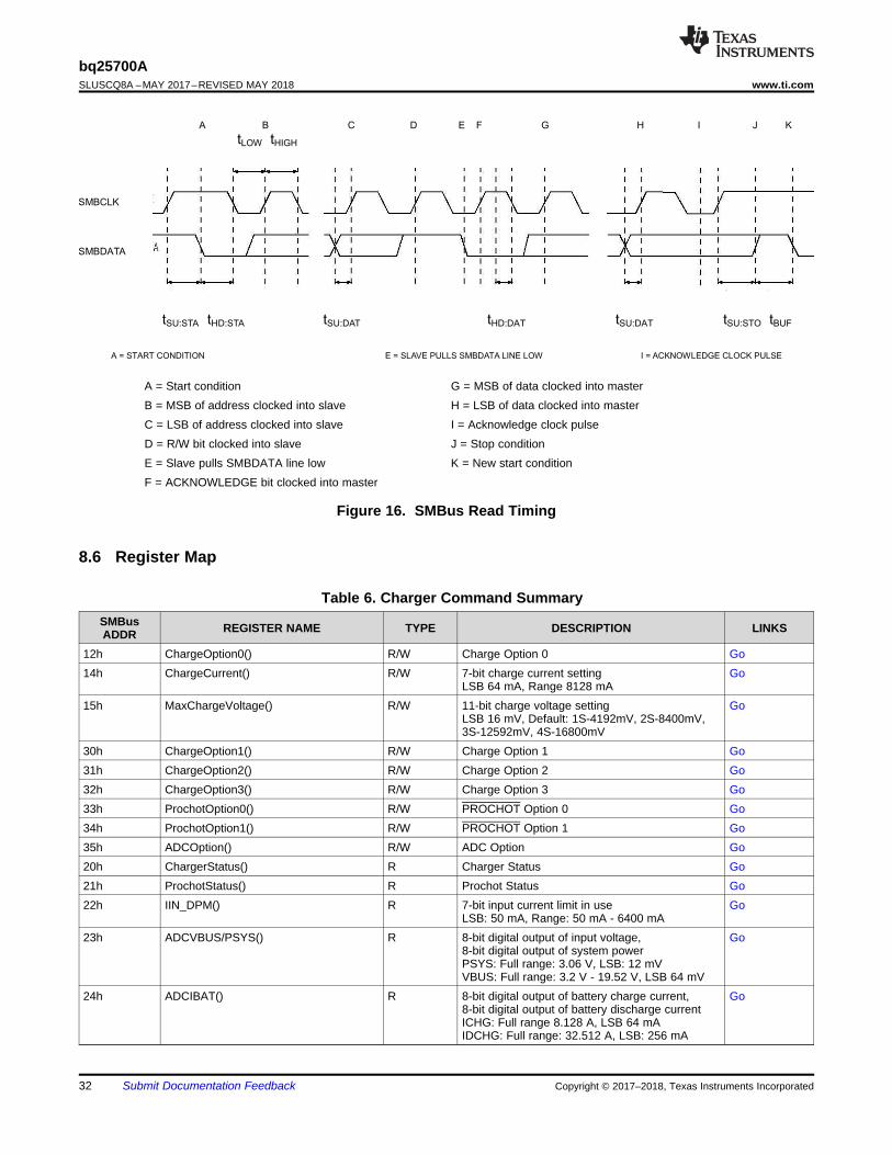
8.5.1.2 Timing Diagrams
A = Start condition H = LSB of data clocked into slaveB = MSB of address clocked into slave I = Slave pulls SMBDATA line lowC = LSB of address clocked into slave J = Acknowledge clocked into masterD = R/W bit clocked into slave K = Acknowledge clock pulseE = Slave pulls SMBDATA line low L = Stop condition, data executed by slaveF = ACKNOWLEDGE bit clocked into master M = New start conditionG = MSB of data clocked into slave
Figure 15. SMBus Write Timing
A B C D E F G H I J K
tLOW tHIGH
SMBCLK
SMBDATA
tSU:STA t tHD:STA SU:DAT HD:DAT SU:DATt t tSU:STO tBUF
A = START CONDITION E = SLAVE PULLS SMBDATA LINE LOW I = ACKNOWLEDGE CLOCK PULSE
32
bq25700ASLUSCQ8A –MAY 2017–REVISED MAY 2018 www.ti.com
Submit Documentation Feedback Copyright © 2017–2018, Texas Instruments Incorporated
A = Start condition G = MSB of data clocked into masterB = MSB of address clocked into slave H = LSB of data clocked into masterC = LSB of address clocked into slave I = Acknowledge clock pulseD = R/W bit clocked into slave J = Stop conditionE = Slave pulls SMBDATA line low K = New start conditionF = ACKNOWLEDGE bit clocked into master
Figure 16. SMBus Read Timing
8.6 Register Map
Table 6. Charger Command SummarySMBusADDR REGISTER NAME TYPE DESCRIPTION LINKS
12h ChargeOption0() R/W Charge Option 0 Go14h ChargeCurrent() R/W 7-bit charge current setting
LSB 64 mA, Range 8128 mAGo
15h MaxChargeVoltage() R/W 11-bit charge voltage settingLSB 16 mV, Default: 1S-4192mV, 2S-8400mV,3S-12592mV, 4S-16800mV
Go
30h ChargeOption1() R/W Charge Option 1 Go31h ChargeOption2() R/W Charge Option 2 Go32h ChargeOption3() R/W Charge Option 3 Go33h ProchotOption0() R/W PROCHOT Option 0 Go34h ProchotOption1() R/W PROCHOT Option 1 Go35h ADCOption() R/W ADC Option Go20h ChargerStatus() R Charger Status Go21h ProchotStatus() R Prochot Status Go22h IIN_DPM() R 7-bit input current limit in use
LSB: 50 mA, Range: 50 mA - 6400 mAGo
23h ADCVBUS/PSYS() R 8-bit digital output of input voltage,8-bit digital output of system powerPSYS: Full range: 3.06 V, LSB: 12 mVVBUS: Full range: 3.2 V - 19.52 V, LSB 64 mV
Go
24h ADCIBAT() R 8-bit digital output of battery charge current,8-bit digital output of battery discharge currentICHG: Full range 8.128 A, LSB 64 mAIDCHG: Full range: 32.512 A, LSB: 256 mA
Go
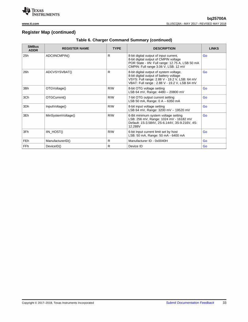
33
bq25700Awww.ti.com SLUSCQ8A –MAY 2017–REVISED MAY 2018
Submit Documentation FeedbackCopyright © 2017–2018, Texas Instruments Incorporated
Register Map (continued)Table 6. Charger Command Summary (continued)
SMBusADDR REGISTER NAME TYPE DESCRIPTION LINKS
25h ADCIINCMPIN() R 8-bit digital output of input current,8-bit digital output of CMPIN voltagePOR State - IIN: Full range: 12.75 A, LSB 50 mACMPIN: Full range 3.06 V, LSB: 12 mV
Go
26h ADCVSYSVBAT() R 8-bit digital output of system voltage,8-bit digital output of battery voltageVSYS: Full range: 2.88 V - 19.2 V, LSB: 64 mVVBAT: Full range : 2.88 V - 19.2 V, LSB 64 mV
Go
3Bh OTGVoltage() R/W 8-bit OTG voltage settingLSB 64 mV, Range: 4480 – 20800 mV
Go
3Ch OTGCurrent() R/W 7-bit OTG output current settingLSB 50 mA, Range: 0 A – 6350 mA
Go
3Dh InputVoltage() R/W 8-bit input voltage settingLSB 64 mV, Range: 3200 mV – 19520 mV
Go
3Eh MinSystemVoltage() R/W 6-Bit minimum system voltage settingLSB: 256 mV, Range: 1024 mV - 16182 mVDefault: 1S-3.584V, 2S-6.144V, 3S-9.216V, 4S-12.288V
Go
3Fh IIN_HOST() R/W 6-bit Input current limit set by hostLSB: 50 mA, Range: 50 mA - 6400 mA
Go
FEh ManufacturerID() R Manufacturer ID - 0x0040H GoFFh DeviceID() R Device ID Go
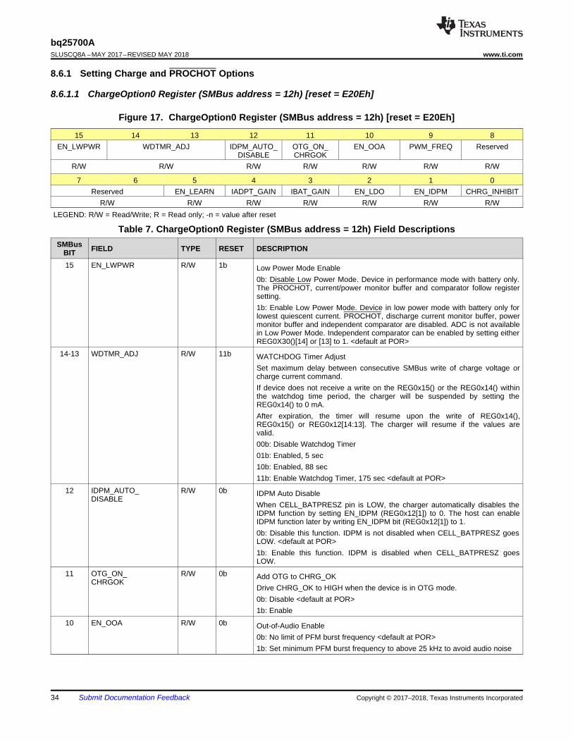
34
bq25700ASLUSCQ8A –MAY 2017–REVISED MAY 2018 www.ti.com
Submit Documentation Feedback Copyright © 2017–2018, Texas Instruments Incorporated
8.6.1 Setting Charge and PROCHOT Options
8.6.1.1 ChargeOption0 Register (SMBus address = 12h) [reset = E20Eh]
Figure 17. ChargeOption0 Register (SMBus address = 12h) [reset = E20Eh]
15 14 13 12 11 10 9 8EN_LWPWR WDTMR_ADJ IDPM_AUTO_
DISABLEOTG_ON_CHRGOK
EN_OOA PWM_FREQ Reserved
R/W R/W R/W R/W R/W R/W R/W
7 6 5 4 3 2 1 0Reserved EN_LEARN IADPT_GAIN IBAT_GAIN EN_LDO EN_IDPM CHRG_INHIBIT
R/W R/W R/W R/W R/W R/W R/WLEGEND: R/W = Read/Write; R = Read only; -n = value after reset
Table 7. ChargeOption0 Register (SMBus address = 12h) Field DescriptionsSMBus
BIT FIELD TYPE RESET DESCRIPTION
15 EN_LWPWR R/W 1b Low Power Mode Enable0b: Disable Low Power Mode. Device in performance mode with battery only.The PROCHOT, current/power monitor buffer and comparator follow registersetting.1b: Enable Low Power Mode. Device in low power mode with battery only forlowest quiescent current. PROCHOT, discharge current monitor buffer, powermonitor buffer and independent comparator are disabled. ADC is not availablein Low Power Mode. Independent comparator can be enabled by setting eitherREG0X30()[14] or [13] to 1. <default at POR>
14-13 WDTMR_ADJ R/W 11b WATCHDOG Timer AdjustSet maximum delay between consecutive SMBus write of charge voltage orcharge current command.If device does not receive a write on the REG0x15() or the REG0x14() withinthe watchdog time period, the charger will be suspended by setting theREG0x14() to 0 mA.After expiration, the timer will resume upon the write of REG0x14(),REG0x15() or REG0x12[14:13]. The charger will resume if the values arevalid.00b: Disable Watchdog Timer01b: Enabled, 5 sec10b: Enabled, 88 sec11b: Enable Watchdog Timer, 175 sec <default at POR>
12 IDPM_AUTO_DISABLE
R/W 0b IDPM Auto DisableWhen CELL_BATPRESZ pin is LOW, the charger automatically disables theIDPM function by setting EN_IDPM (REG0x12[1]) to 0. The host can enableIDPM function later by writing EN_IDPM bit (REG0x12[1]) to 1.0b: Disable this function. IDPM is not disabled when CELL_BATPRESZ goesLOW. <default at POR>1b: Enable this function. IDPM is disabled when CELL_BATPRESZ goesLOW.
11 OTG_ON_CHRGOK
R/W 0b Add OTG to CHRG_OKDrive CHRG_OK to HIGH when the device is in OTG mode.0b: Disable <default at POR>1b: Enable
10 EN_OOA R/W 0b Out-of-Audio Enable0b: No limit of PFM burst frequency <default at POR>1b: Set minimum PFM burst frequency to above 25 kHz to avoid audio noise
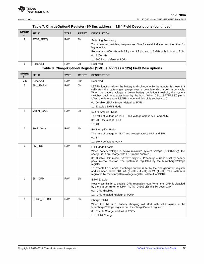
35
bq25700Awww.ti.com SLUSCQ8A –MAY 2017–REVISED MAY 2018
Submit Documentation FeedbackCopyright © 2017–2018, Texas Instruments Incorporated
Table 7. ChargeOption0 Register (SMBus address = 12h) Field Descriptions (continued)SMBus
BIT FIELD TYPE RESET DESCRIPTION
9 PWM_FREQ R/W 1b Switching FrequencyTwo converter switching frequencies. One for small inductor and the other forbig inductor.Recommend 800 kHz with 2.2 µH or 3.3 µH, and 1.2 MHz with 1 µH or 1.5 µH.0b: 1200 kHz1b: 800 kHz <default at POR>
8 Reserved R/W 0b Reserved
Table 8. ChargeOption0 Register (SMBus address = 12h) Field DescriptionsSMBus
BIT FIELD TYPE RESET DESCRIPTION
7-6 Reserved R/W 00b Reserved5 EN_LEARN R/W 0b LEARN function allows the battery to discharge while the adapter is present. It
calibrates the battery gas gauge over a complete discharge/charge cycle.When the battery voltage is below battery depletion threshold, the systemswitches back to adapter input by the host. When CELL_BATPRESZ pin isLOW, the device exits LEARN mode and this bit is set back to 0.0b: Disable LEARN Mode <default at POR>1b: Enable LEARN Mode
4 IADPT_GAIN R/W 0b IADPT Amplifier RatioThe ratio of voltage on IADPT and voltage across ACP and ACN.0b: 20× <default at POR>1b: 40×
3 IBAT_GAIN R/W 1b IBAT Amplifier RatioThe ratio of voltage on IBAT and voltage across SRP and SRN0b: 8×1b: 16× <default at POR>
2 EN_LDO R/W 1b LDO Mode EnableWhen battery voltage is below minimum system voltage (REG0x3E()), thecharger is in pre-charge with LDO mode enabled.0b: Disable LDO mode, BATFET fully ON. Precharge current is set by batterypack internal resistor. The system is regulated by the MaxChargeVoltageregister.1b: Enable LDO mode, Precharge current is set by the ChargeCurrent registerand clamped below 384 mA (2 cell – 4 cell) or 2A (1 cell). The system isregulated by the MinSystemVoltage register. <default at POR>
1 EN_IDPM R/W 1b IDPM EnableHost writes this bit to enable IDPM regulation loop. When the IDPM is disabledby the charger (refer to IDPM_AUTO_DISABLE), this bit goes LOW.0b: IDPM disabled1b: IDPM enabled <default at POR>
0 CHRG_INHIBIT R/W 0b Charge InhibitWhen this bit is 0, battery charging will start with valid values in theMaxChargeVoltage register and the ChargeCurrent register.0b: Enable Charge <default at POR>1b: Inhibit Charge
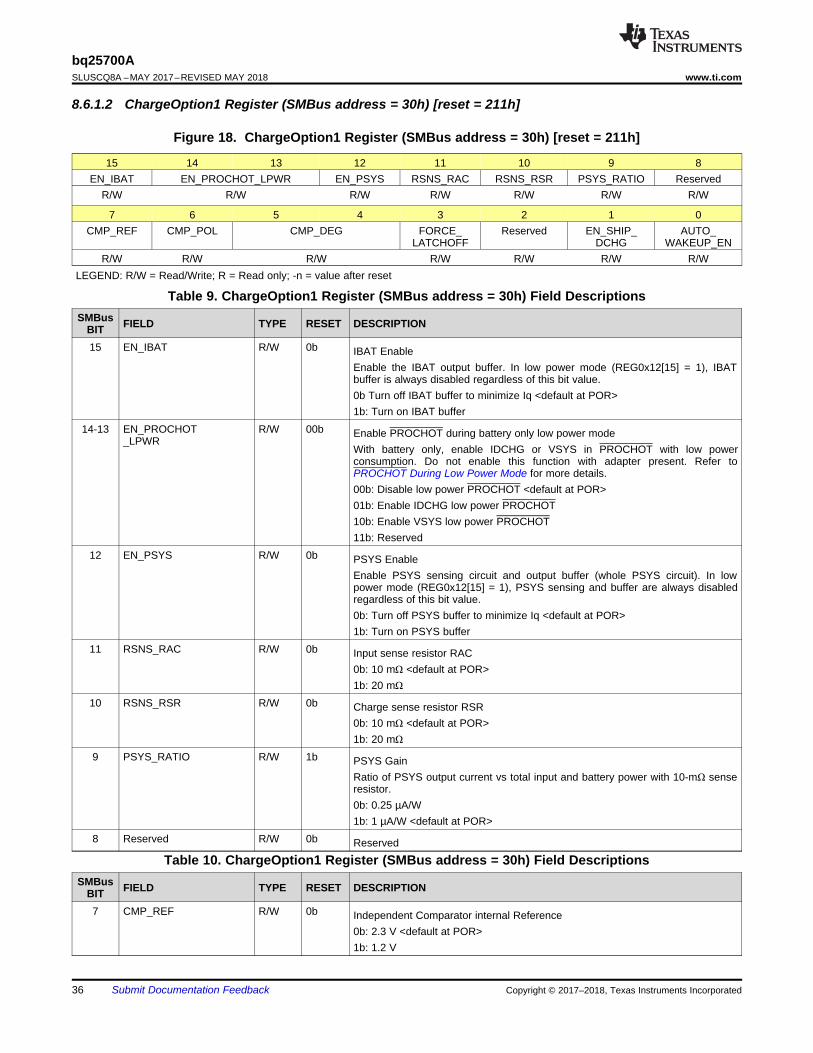
36
bq25700ASLUSCQ8A –MAY 2017–REVISED MAY 2018 www.ti.com
Submit Documentation Feedback Copyright © 2017–2018, Texas Instruments Incorporated
8.6.1.2 ChargeOption1 Register (SMBus address = 30h) [reset = 211h]
Figure 18. ChargeOption1 Register (SMBus address = 30h) [reset = 211h]
15 14 13 12 11 10 9 8EN_IBAT EN_PROCHOT_LPWR EN_PSYS RSNS_RAC RSNS_RSR PSYS_RATIO Reserved
R/W R/W R/W R/W R/W R/W R/W
7 6 5 4 3 2 1 0CMP_REF CMP_POL CMP_DEG FORCE_
LATCHOFFReserved EN_SHIP_
DCHGAUTO_
WAKEUP_ENR/W R/W R/W R/W R/W R/W R/W
LEGEND: R/W = Read/Write; R = Read only; -n = value after reset
Table 9. ChargeOption1 Register (SMBus address = 30h) Field DescriptionsSMBus
BIT FIELD TYPE RESET DESCRIPTION
15 EN_IBAT R/W 0b IBAT EnableEnable the IBAT output buffer. In low power mode (REG0x12[15] = 1), IBATbuffer is always disabled regardless of this bit value.0b Turn off IBAT buffer to minimize Iq <default at POR>1b: Turn on IBAT buffer
14-13 EN_PROCHOT_LPWR
R/W 00b Enable PROCHOT during battery only low power modeWith battery only, enable IDCHG or VSYS in PROCHOT with low powerconsumption. Do not enable this function with adapter present. Refer toPROCHOT During Low Power Mode for more details.00b: Disable low power PROCHOT <default at POR>01b: Enable IDCHG low power PROCHOT10b: Enable VSYS low power PROCHOT11b: Reserved
12 EN_PSYS R/W 0b PSYS EnableEnable PSYS sensing circuit and output buffer (whole PSYS circuit). In lowpower mode (REG0x12[15] = 1), PSYS sensing and buffer are always disabledregardless of this bit value.0b: Turn off PSYS buffer to minimize Iq <default at POR>1b: Turn on PSYS buffer
11 RSNS_RAC R/W 0b Input sense resistor RAC0b: 10 mΩ <default at POR>1b: 20 mΩ
10 RSNS_RSR R/W 0b Charge sense resistor RSR0b: 10 mΩ <default at POR>1b: 20 mΩ
9 PSYS_RATIO R/W 1b PSYS GainRatio of PSYS output current vs total input and battery power with 10-mΩ senseresistor.0b: 0.25 µA/W1b: 1 µA/W <default at POR>
8 Reserved R/W 0b Reserved
Table 10. ChargeOption1 Register (SMBus address = 30h) Field DescriptionsSMBus
BIT FIELD TYPE RESET DESCRIPTION
7 CMP_REF R/W 0b Independent Comparator internal Reference0b: 2.3 V <default at POR>1b: 1.2 V
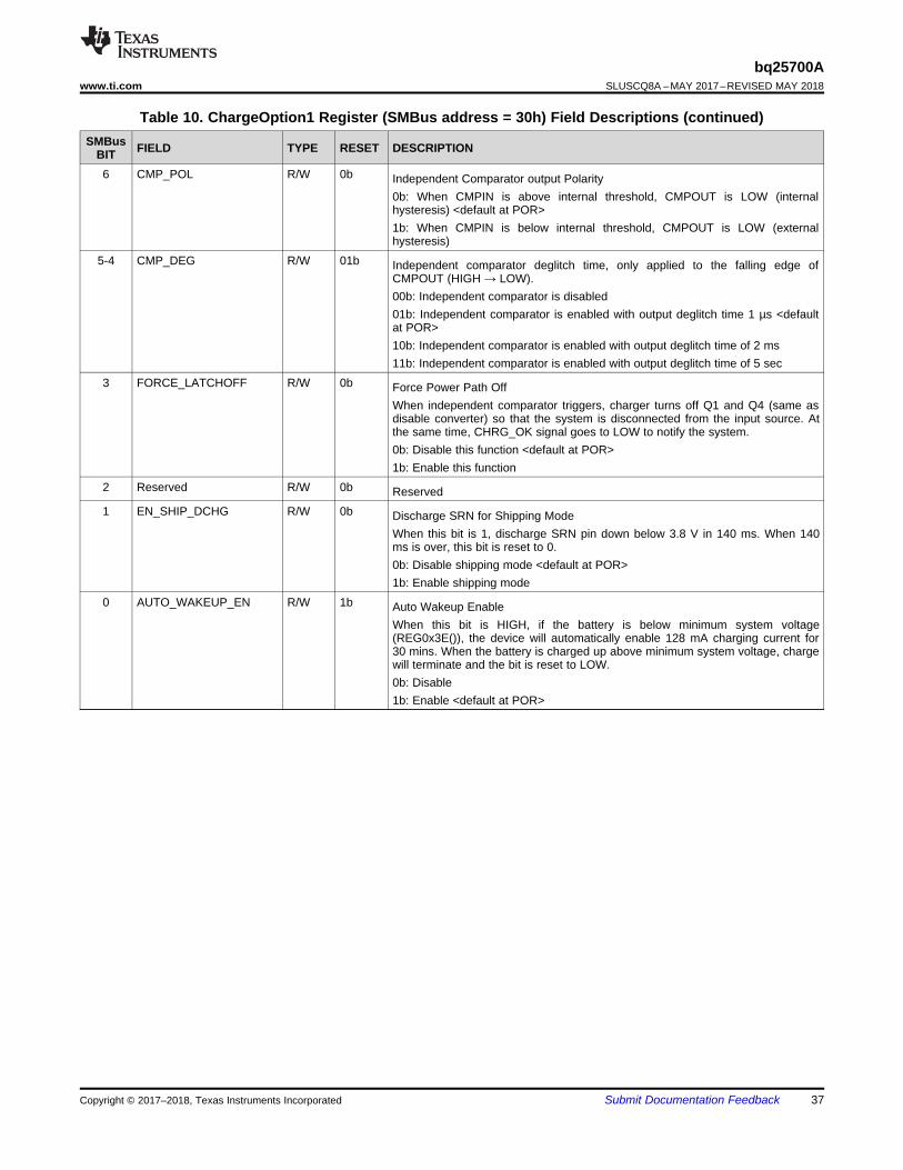
37
bq25700Awww.ti.com SLUSCQ8A –MAY 2017–REVISED MAY 2018
Submit Documentation FeedbackCopyright © 2017–2018, Texas Instruments Incorporated
Table 10. ChargeOption1 Register (SMBus address = 30h) Field Descriptions (continued)SMBus
BIT FIELD TYPE RESET DESCRIPTION
6 CMP_POL R/W 0b Independent Comparator output Polarity0b: When CMPIN is above internal threshold, CMPOUT is LOW (internalhysteresis) <default at POR>1b: When CMPIN is below internal threshold, CMPOUT is LOW (externalhysteresis)
5-4 CMP_DEG R/W 01b Independent comparator deglitch time, only applied to the falling edge ofCMPOUT (HIGH → LOW).00b: Independent comparator is disabled01b: Independent comparator is enabled with output deglitch time 1 µs <defaultat POR>10b: Independent comparator is enabled with output deglitch time of 2 ms11b: Independent comparator is enabled with output deglitch time of 5 sec
3 FORCE_LATCHOFF R/W 0b Force Power Path OffWhen independent comparator triggers, charger turns off Q1 and Q4 (same asdisable converter) so that the system is disconnected from the input source. Atthe same time, CHRG_OK signal goes to LOW to notify the system.0b: Disable this function <default at POR>1b: Enable this function
2 Reserved R/W 0b Reserved1 EN_SHIP_DCHG R/W 0b Discharge SRN for Shipping Mode
When this bit is 1, discharge SRN pin down below 3.8 V in 140 ms. When 140ms is over, this bit is reset to 0.0b: Disable shipping mode <default at POR>1b: Enable shipping mode
0 AUTO_WAKEUP_EN R/W 1b Auto Wakeup EnableWhen this bit is HIGH, if the battery is below minimum system voltage(REG0x3E()), the device will automatically enable 128 mA charging current for30 mins. When the battery is charged up above minimum system voltage, chargewill terminate and the bit is reset to LOW.0b: Disable1b: Enable <default at POR>
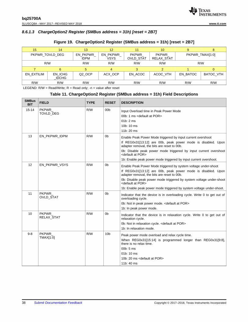
38
bq25700ASLUSCQ8A –MAY 2017–REVISED MAY 2018 www.ti.com
Submit Documentation Feedback Copyright © 2017–2018, Texas Instruments Incorporated
8.6.1.3 ChargeOption2 Register (SMBus address = 31h) [reset = 2B7]
Figure 19. ChargeOption2 Register (SMBus address = 31h) [reset = 2B7]
15 14 13 12 11 10 9 8PKPWR_TOVLD_DEG EN_PKPWR_
IDPMEN_PKPWR_
VSYSPKPWR_
OVLD_STATPKPWR_
RELAX_STATPKPWR_TMAX[1:0]
R/W R/W R/W R/W R/W R/W
7 6 5 4 3 2 1 0EN_EXTILIM EN_ICHG
_IDCHGQ2_OCP ACX_OCP EN_ACOC ACOC_VTH EN_BATOC BATOC_VTH
R/W R/W R/W R/W R/W R/W R/W R/WLEGEND: R/W = Read/Write; R = Read only; -n = value after reset
Table 11. ChargeOption2 Register (SMBus address = 31h) Field DescriptionsSMBus
BIT FIELD TYPE RESET DESCRIPTION
15-14 PKPWR_TOVLD_DEG
R/W 00b Input Overload time in Peak Power Mode00b: 1 ms <default at POR>01b: 2 ms10b: 10 ms11b: 20 ms
13 EN_PKPWR_IDPM R/W 0b Enable Peak Power Mode triggered by input current overshootIf REG0x31[13:12] are 00b, peak power mode is disabled. Uponadapter removal, the bits are reset to 00b.0b: Disable peak power mode triggered by input current overshoot<default at POR>1b: Enable peak power mode triggered by input current overshoot.
12 EN_PKPWR_VSYS R/W 0b Enable Peak Power Mode triggered by system voltage under-shootIf REG0x31[13:12] are 00b, peak power mode is disabled. Uponadapter removal, the bits are reset to 00b.0b: Disable peak power mode triggered by system voltage under-shoot<default at POR>1b: Enable peak power mode triggered by system voltage under-shoot.
11 PKPWR_OVLD_STAT
R/W 0b Indicator that the device is in overloading cycle. Write 0 to get out ofoverloading cycle.0b: Not in peak power mode. <default at POR>1b: In peak power mode.
10 PKPWR_RELAX_STAT
R/W 0b Indicator that the device is in relaxation cycle. Write 0 to get out ofrelaxation cycle.0b: Not in relaxation cycle. <default at POR>1b: In relaxation mode.
9-8 PKPWR_TMAX[1:0]
R/W 10b Peak power mode overload and relax cycle time.When REG0x31[15:14] is programmed longer than REG0x31[9:8],there is no relax time.00b: 5 ms01b: 10 ms10b: 20 ms <default at POR>11b: 40 ms
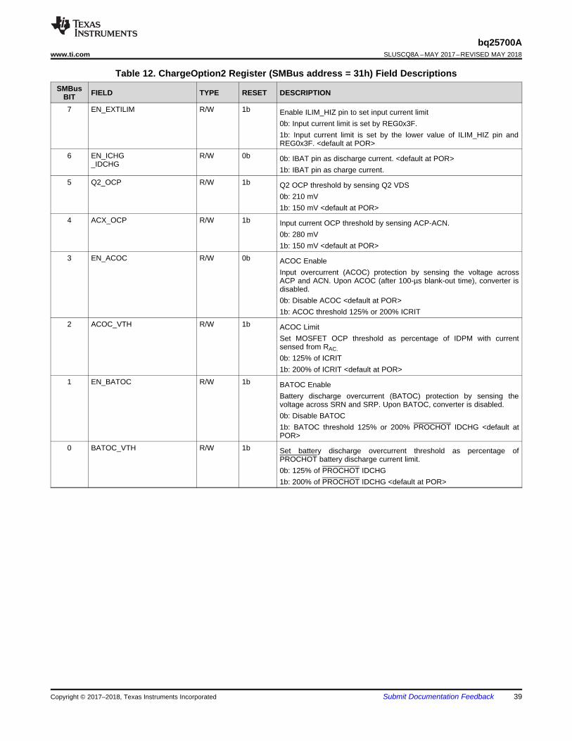
39
bq25700Awww.ti.com SLUSCQ8A –MAY 2017–REVISED MAY 2018
Submit Documentation FeedbackCopyright © 2017–2018, Texas Instruments Incorporated
Table 12. ChargeOption2 Register (SMBus address = 31h) Field DescriptionsSMBus
BIT FIELD TYPE RESET DESCRIPTION
7 EN_EXTILIM R/W 1b Enable ILIM_HIZ pin to set input current limit0b: Input current limit is set by REG0x3F.1b: Input current limit is set by the lower value of ILIM_HIZ pin andREG0x3F. <default at POR>
6 EN_ICHG_IDCHG
R/W 0b 0b: IBAT pin as discharge current. <default at POR>1b: IBAT pin as charge current.
5 Q2_OCP R/W 1b Q2 OCP threshold by sensing Q2 VDS0b: 210 mV1b: 150 mV <default at POR>
4 ACX_OCP R/W 1b Input current OCP threshold by sensing ACP-ACN.0b: 280 mV1b: 150 mV <default at POR>
3 EN_ACOC R/W 0b ACOC EnableInput overcurrent (ACOC) protection by sensing the voltage acrossACP and ACN. Upon ACOC (after 100-µs blank-out time), converter isdisabled.0b: Disable ACOC <default at POR>1b: ACOC threshold 125% or 200% ICRIT
2 ACOC_VTH R/W 1b ACOC LimitSet MOSFET OCP threshold as percentage of IDPM with currentsensed from RAC.
0b: 125% of ICRIT1b: 200% of ICRIT <default at POR>
1 EN_BATOC R/W 1b BATOC EnableBattery discharge overcurrent (BATOC) protection by sensing thevoltage across SRN and SRP. Upon BATOC, converter is disabled.0b: Disable BATOC1b: BATOC threshold 125% or 200% PROCHOT IDCHG <default atPOR>
0 BATOC_VTH R/W 1b Set battery discharge overcurrent threshold as percentage ofPROCHOT battery discharge current limit.0b: 125% of PROCHOT IDCHG1b: 200% of PROCHOT IDCHG <default at POR>
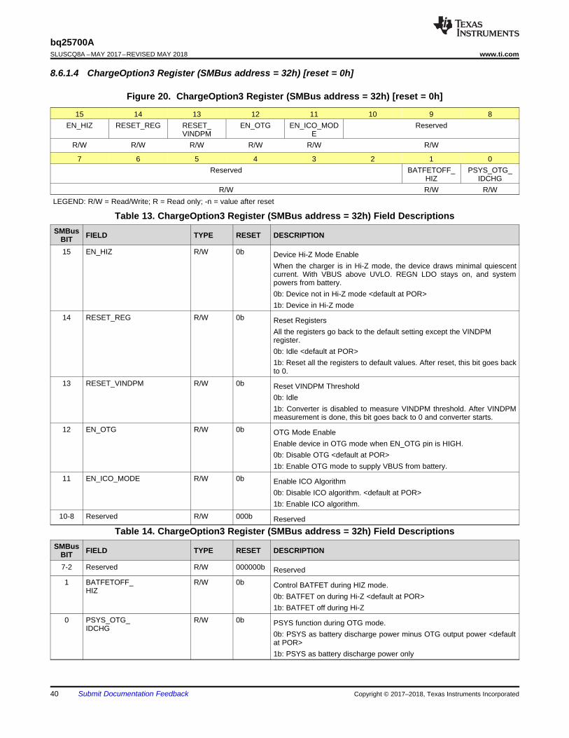
40
bq25700ASLUSCQ8A –MAY 2017–REVISED MAY 2018 www.ti.com
Submit Documentation Feedback Copyright © 2017–2018, Texas Instruments Incorporated
8.6.1.4 ChargeOption3 Register (SMBus address = 32h) [reset = 0h]
Figure 20. ChargeOption3 Register (SMBus address = 32h) [reset = 0h]
15 14 13 12 11 10 9 8EN_HIZ RESET_REG RESET_
VINDPMEN_OTG EN_ICO_MOD
EReserved
R/W R/W R/W R/W R/W R/W
7 6 5 4 3 2 1 0Reserved BATFETOFF_
HIZPSYS_OTG_
IDCHGR/W R/W R/W
LEGEND: R/W = Read/Write; R = Read only; -n = value after reset
Table 13. ChargeOption3 Register (SMBus address = 32h) Field DescriptionsSMBus
BIT FIELD TYPE RESET DESCRIPTION
15 EN_HIZ R/W 0b Device Hi-Z Mode EnableWhen the charger is in Hi-Z mode, the device draws minimal quiescentcurrent. With VBUS above UVLO. REGN LDO stays on, and systempowers from battery.0b: Device not in Hi-Z mode <default at POR>1b: Device in Hi-Z mode
14 RESET_REG R/W 0b Reset RegistersAll the registers go back to the default setting except the VINDPMregister.0b: Idle <default at POR>1b: Reset all the registers to default values. After reset, this bit goes backto 0.
13 RESET_VINDPM R/W 0b Reset VINDPM Threshold0b: Idle1b: Converter is disabled to measure VINDPM threshold. After VINDPMmeasurement is done, this bit goes back to 0 and converter starts.
12 EN_OTG R/W 0b OTG Mode EnableEnable device in OTG mode when EN_OTG pin is HIGH.0b: Disable OTG <default at POR>1b: Enable OTG mode to supply VBUS from battery.
11 EN_ICO_MODE R/W 0b Enable ICO Algorithm0b: Disable ICO algorithm. <default at POR>1b: Enable ICO algorithm.
10-8 Reserved R/W 000b Reserved
Table 14. ChargeOption3 Register (SMBus address = 32h) Field DescriptionsSMBus
BIT FIELD TYPE RESET DESCRIPTION
7-2 Reserved R/W 000000b Reserved1 BATFETOFF_
HIZR/W 0b Control BATFET during HIZ mode.
0b: BATFET on during Hi-Z <default at POR>1b: BATFET off during Hi-Z
0 PSYS_OTG_IDCHG
R/W 0b PSYS function during OTG mode.0b: PSYS as battery discharge power minus OTG output power <defaultat POR>1b: PSYS as battery discharge power only
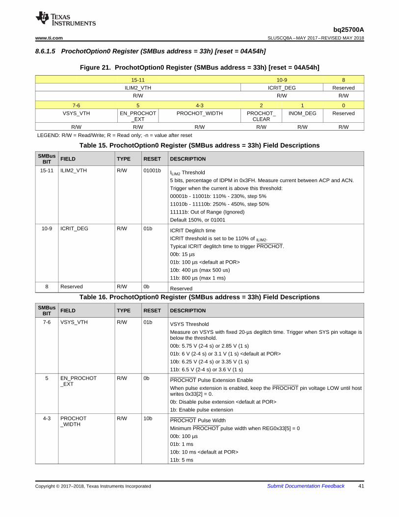
41
bq25700Awww.ti.com SLUSCQ8A –MAY 2017–REVISED MAY 2018
Submit Documentation FeedbackCopyright © 2017–2018, Texas Instruments Incorporated
8.6.1.5 ProchotOption0 Register (SMBus address = 33h) [reset = 04A54h]
Figure 21. ProchotOption0 Register (SMBus address = 33h) [reset = 04A54h]
15-11 10-9 8ILIM2_VTH ICRIT_DEG Reserved
R/W R/W R/W
7-6 5 4-3 2 1 0VSYS_VTH EN_PROCHOT
_EXTPROCHOT_WIDTH PROCHOT_
CLEARINOM_DEG Reserved
R/W R/W R/W R/W R/W R/WLEGEND: R/W = Read/Write; R = Read only; -n = value after reset
Table 15. ProchotOption0 Register (SMBus address = 33h) Field DescriptionsSMBus
BIT FIELD TYPE RESET DESCRIPTION
15-11 ILIM2_VTH R/W 01001b ILIM2 Threshold5 bits, percentage of IDPM in 0x3FH. Measure current between ACP and ACN.Trigger when the current is above this threshold:00001b - 11001b: 110% - 230%, step 5%11010b - 11110b: 250% - 450%, step 50%11111b: Out of Range (Ignored)Default 150%, or 01001
10-9 ICRIT_DEG R/W 01b ICRIT Deglitch timeICRIT threshold is set to be 110% of ILIM2.Typical ICRIT deglitch time to trigger PROCHOT.00b: 15 µs01b: 100 µs <default at POR>10b: 400 µs (max 500 us)11b: 800 µs (max 1 ms)
8 Reserved R/W 0b Reserved
Table 16. ProchotOption0 Register (SMBus address = 33h) Field DescriptionsSMBus
BIT FIELD TYPE RESET DESCRIPTION
7-6 VSYS_VTH R/W 01b VSYS ThresholdMeasure on VSYS with fixed 20-µs deglitch time. Trigger when SYS pin voltage isbelow the threshold.00b: 5.75 V (2-4 s) or 2.85 V (1 s)01b: 6 V (2-4 s) or 3.1 V (1 s) <default at POR>10b: 6.25 V (2-4 s) or 3.35 V (1 s)11b: 6.5 V (2-4 s) or 3.6 V (1 s)
5 EN_PROCHOT_EXT
R/W 0b PROCHOT Pulse Extension EnableWhen pulse extension is enabled, keep the PROCHOT pin voltage LOW until hostwrites 0x33[2] = 0.0b: Disable pulse extension <default at POR>1b: Enable pulse extension
4-3 PROCHOT_WIDTH
R/W 10b PROCHOT Pulse WidthMinimum PROCHOT pulse width when REG0x33[5] = 000b: 100 µs01b: 1 ms10b: 10 ms <default at POR>11b: 5 ms
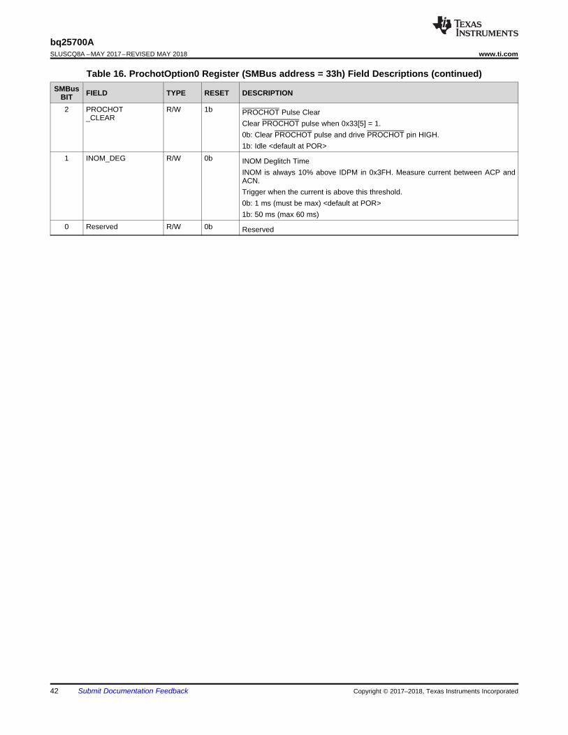
42
bq25700ASLUSCQ8A –MAY 2017–REVISED MAY 2018 www.ti.com
Submit Documentation Feedback Copyright © 2017–2018, Texas Instruments Incorporated
Table 16. ProchotOption0 Register (SMBus address = 33h) Field Descriptions (continued)SMBus
BIT FIELD TYPE RESET DESCRIPTION
2 PROCHOT_CLEAR
R/W 1b PROCHOT Pulse ClearClear PROCHOT pulse when 0x33[5] = 1.0b: Clear PROCHOT pulse and drive PROCHOT pin HIGH.1b: Idle <default at POR>
1 INOM_DEG R/W 0b INOM Deglitch TimeINOM is always 10% above IDPM in 0x3FH. Measure current between ACP andACN.Trigger when the current is above this threshold.0b: 1 ms (must be max) <default at POR>1b: 50 ms (max 60 ms)
0 Reserved R/W 0b Reserved
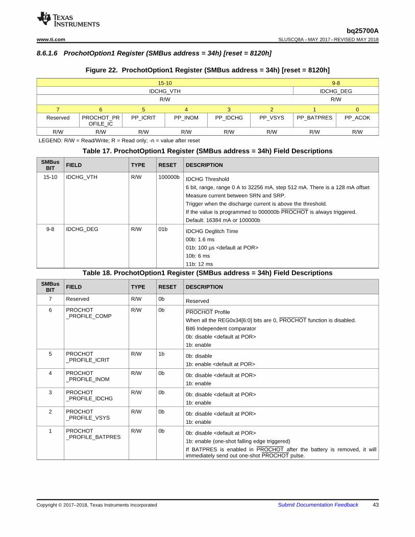
43
bq25700Awww.ti.com SLUSCQ8A –MAY 2017–REVISED MAY 2018
Submit Documentation FeedbackCopyright © 2017–2018, Texas Instruments Incorporated
8.6.1.6 ProchotOption1 Register (SMBus address = 34h) [reset = 8120h]
Figure 22. ProchotOption1 Register (SMBus address = 34h) [reset = 8120h]
15-10 9-8IDCHG_VTH IDCHG_DEG
R/W R/W
7 6 5 4 3 2 1 0Reserved PROCHOT_PR
OFILE_ICPP_ICRIT PP_INOM PP_IDCHG PP_VSYS PP_BATPRES PP_ACOK
R/W R/W R/W R/W R/W R/W R/W R/WLEGEND: R/W = Read/Write; R = Read only; -n = value after reset
Table 17. ProchotOption1 Register (SMBus address = 34h) Field DescriptionsSMBus
BIT FIELD TYPE RESET DESCRIPTION
15-10 IDCHG_VTH R/W 100000b IDCHG Threshold6 bit, range, range 0 A to 32256 mA, step 512 mA. There is a 128 mA offsetMeasure current between SRN and SRP.Trigger when the discharge current is above the threshold.If the value is programmed to 000000b PROCHOT is always triggered.Default: 16384 mA or 100000b
9-8 IDCHG_DEG R/W 01b IDCHG Deglitch Time00b: 1.6 ms01b: 100 µs <default at POR>10b: 6 ms11b: 12 ms
Table 18. ProchotOption1 Register (SMBus address = 34h) Field DescriptionsSMBus
BIT FIELD TYPE RESET DESCRIPTION
7 Reserved R/W 0b Reserved6 PROCHOT
_PROFILE_COMPR/W 0b PROCHOT Profile
When all the REG0x34[6:0] bits are 0, PROCHOT function is disabled.Bit6 Independent comparator0b: disable <default at POR>1b: enable
5 PROCHOT_PROFILE_ICRIT
R/W 1b 0b: disable1b: enable <default at POR>
4 PROCHOT_PROFILE_INOM
R/W 0b 0b: disable <default at POR>1b: enable
3 PROCHOT_PROFILE_IDCHG
R/W 0b 0b: disable <default at POR>1b: enable
2 PROCHOT_PROFILE_VSYS
R/W 0b 0b: disable <default at POR>1b: enable
1 PROCHOT_PROFILE_BATPRES
R/W 0b 0b: disable <default at POR>1b: enable (one-shot falling edge triggered)If BATPRES is enabled in PROCHOT after the battery is removed, it willimmediately send out one-shot PROCHOT pulse.
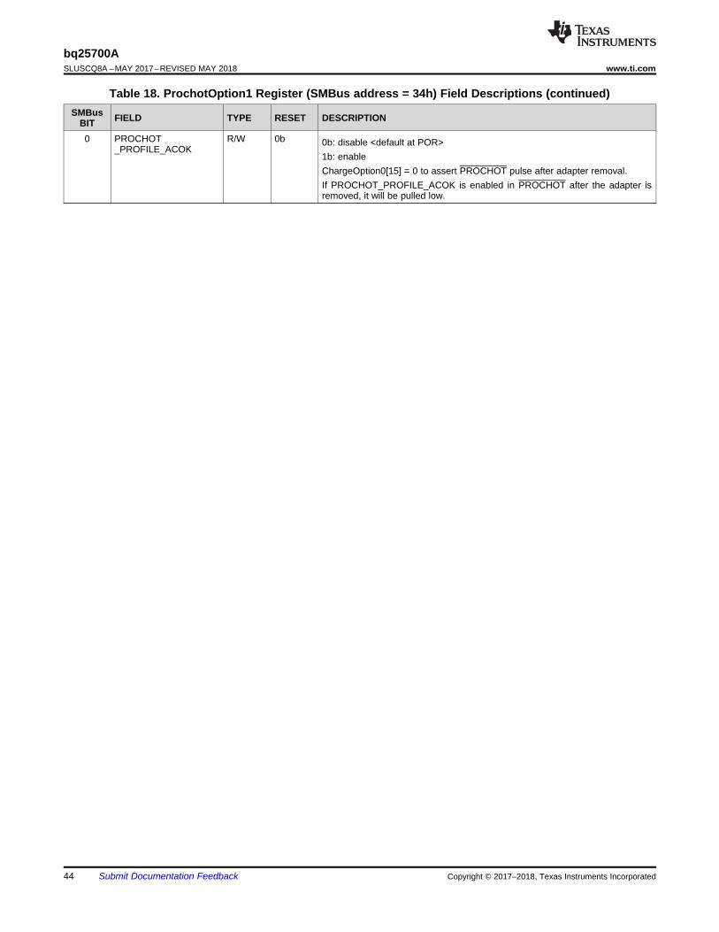
44
bq25700ASLUSCQ8A –MAY 2017–REVISED MAY 2018 www.ti.com
Submit Documentation Feedback Copyright © 2017–2018, Texas Instruments Incorporated
Table 18. ProchotOption1 Register (SMBus address = 34h) Field Descriptions (continued)SMBus
BIT FIELD TYPE RESET DESCRIPTION
0 PROCHOT_PROFILE_ACOK
R/W 0b 0b: disable <default at POR>1b: enableChargeOption0[15] = 0 to assert PROCHOT pulse after adapter removal.If PROCHOT_PROFILE_ACOK is enabled in PROCHOT after the adapter isremoved, it will be pulled low.
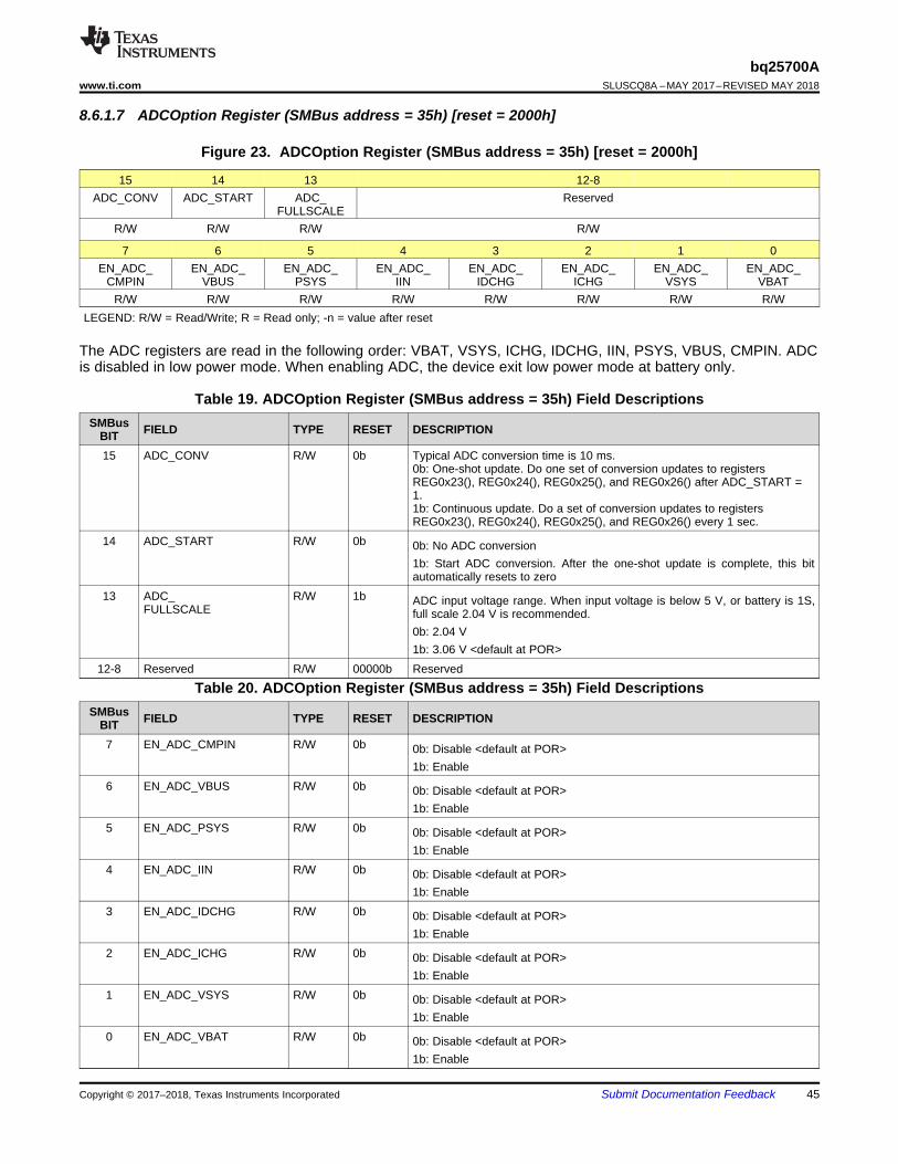
45
bq25700Awww.ti.com SLUSCQ8A –MAY 2017–REVISED MAY 2018
Submit Documentation FeedbackCopyright © 2017–2018, Texas Instruments Incorporated
8.6.1.7 ADCOption Register (SMBus address = 35h) [reset = 2000h]
Figure 23. ADCOption Register (SMBus address = 35h) [reset = 2000h]
15 14 13 12-8ADC_CONV ADC_START ADC_
FULLSCALEReserved
R/W R/W R/W R/W
7 6 5 4 3 2 1 0EN_ADC_
CMPINEN_ADC_
VBUSEN_ADC_
PSYSEN_ADC_
IINEN_ADC_
IDCHGEN_ADC_
ICHGEN_ADC_
VSYSEN_ADC_
VBATR/W R/W R/W R/W R/W R/W R/W R/W
LEGEND: R/W = Read/Write; R = Read only; -n = value after reset
The ADC registers are read in the following order: VBAT, VSYS, ICHG, IDCHG, IIN, PSYS, VBUS, CMPIN. ADCis disabled in low power mode. When enabling ADC, the device exit low power mode at battery only.
Table 19. ADCOption Register (SMBus address = 35h) Field DescriptionsSMBus
BIT FIELD TYPE RESET DESCRIPTION
15 ADC_CONV R/W 0b Typical ADC conversion time is 10 ms.0b: One-shot update. Do one set of conversion updates to registersREG0x23(), REG0x24(), REG0x25(), and REG0x26() after ADC_START =1.1b: Continuous update. Do a set of conversion updates to registersREG0x23(), REG0x24(), REG0x25(), and REG0x26() every 1 sec.
14 ADC_START R/W 0b 0b: No ADC conversion1b: Start ADC conversion. After the one-shot update is complete, this bitautomatically resets to zero
13 ADC_FULLSCALE
R/W 1b ADC input voltage range. When input voltage is below 5 V, or battery is 1S,full scale 2.04 V is recommended.0b: 2.04 V1b: 3.06 V <default at POR>
12-8 Reserved R/W 00000b Reserved
Table 20. ADCOption Register (SMBus address = 35h) Field DescriptionsSMBus
BIT FIELD TYPE RESET DESCRIPTION
7 EN_ADC_CMPIN R/W 0b 0b: Disable <default at POR>1b: Enable
6 EN_ADC_VBUS R/W 0b 0b: Disable <default at POR>1b: Enable
5 EN_ADC_PSYS R/W 0b 0b: Disable <default at POR>1b: Enable
4 EN_ADC_IIN R/W 0b 0b: Disable <default at POR>1b: Enable
3 EN_ADC_IDCHG R/W 0b 0b: Disable <default at POR>1b: Enable
2 EN_ADC_ICHG R/W 0b 0b: Disable <default at POR>1b: Enable
1 EN_ADC_VSYS R/W 0b 0b: Disable <default at POR>1b: Enable
0 EN_ADC_VBAT R/W 0b 0b: Disable <default at POR>1b: Enable
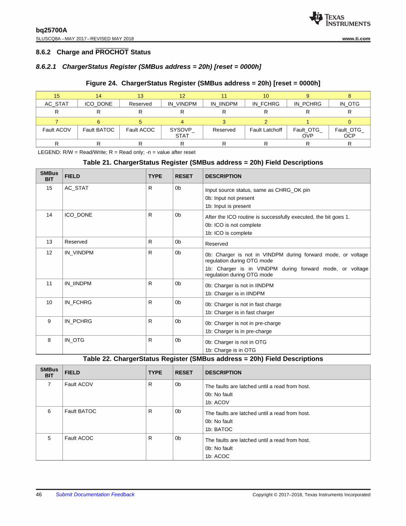
46
bq25700ASLUSCQ8A –MAY 2017–REVISED MAY 2018 www.ti.com
Submit Documentation Feedback Copyright © 2017–2018, Texas Instruments Incorporated
8.6.2 Charge and PROCHOT Status
8.6.2.1 ChargerStatus Register (SMBus address = 20h) [reset = 0000h]
Figure 24. ChargerStatus Register (SMBus address = 20h) [reset = 0000h]
15 14 13 12 11 10 9 8AC_STAT ICO_DONE Reserved IN_VINDPM IN_IINDPM IN_FCHRG IN_PCHRG IN_OTG
R R R R R R R R
7 6 5 4 3 2 1 0Fault ACOV Fault BATOC Fault ACOC SYSOVP_
STATReserved Fault Latchoff Fault_OTG_
OVPFault_OTG_
OCPR R R R R R R R
LEGEND: R/W = Read/Write; R = Read only; -n = value after reset
Table 21. ChargerStatus Register (SMBus address = 20h) Field DescriptionsSMBus
BIT FIELD TYPE RESET DESCRIPTION
15 AC_STAT R 0b Input source status, same as CHRG_OK pin0b: Input not present1b: Input is present
14 ICO_DONE R 0b After the ICO routine is successfully executed, the bit goes 1.0b: ICO is not complete1b: ICO is complete
13 Reserved R 0b Reserved12 IN_VINDPM R 0b 0b: Charger is not in VINDPM during forward mode, or voltage
regulation during OTG mode1b: Charger is in VINDPM during forward mode, or voltageregulation during OTG mode
11 IN_IINDPM R 0b 0b: Charger is not in IINDPM1b: Charger is in IINDPM
10 IN_FCHRG R 0b 0b: Charger is not in fast charge1b: Charger is in fast charger
9 IN_PCHRG R 0b 0b: Charger is not in pre-charge1b: Charger is in pre-charge
8 IN_OTG R 0b 0b: Charger is not in OTG1b: Charge is in OTG
Table 22. ChargerStatus Register (SMBus address = 20h) Field DescriptionsSMBus
BIT FIELD TYPE RESET DESCRIPTION
7 Fault ACOV R 0b The faults are latched until a read from host.0b: No fault1b: ACOV
6 Fault BATOC R 0b The faults are latched until a read from host.0b: No fault1b: BATOC
5 Fault ACOC R 0b The faults are latched until a read from host.0b: No fault1b: ACOC
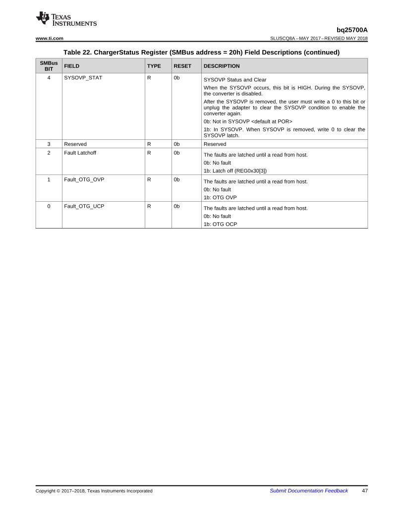
47
bq25700Awww.ti.com SLUSCQ8A –MAY 2017–REVISED MAY 2018
Submit Documentation FeedbackCopyright © 2017–2018, Texas Instruments Incorporated
Table 22. ChargerStatus Register (SMBus address = 20h) Field Descriptions (continued)SMBus
BIT FIELD TYPE RESET DESCRIPTION
4 SYSOVP_STAT R 0b SYSOVP Status and ClearWhen the SYSOVP occurs, this bit is HIGH. During the SYSOVP,the converter is disabled.After the SYSOVP is removed, the user must write a 0 to this bit orunplug the adapter to clear the SYSOVP condition to enable theconverter again.0b: Not in SYSOVP <default at POR>1b: In SYSOVP. When SYSOVP is removed, write 0 to clear theSYSOVP latch.
3 Reserved R 0b Reserved2 Fault Latchoff R 0b The faults are latched until a read from host.
0b: No fault1b: Latch off (REG0x30[3])
1 Fault_OTG_OVP R 0b The faults are latched until a read from host.0b: No fault1b: OTG OVP
0 Fault_OTG_UCP R 0b The faults are latched until a read from host.0b: No fault1b: OTG OCP
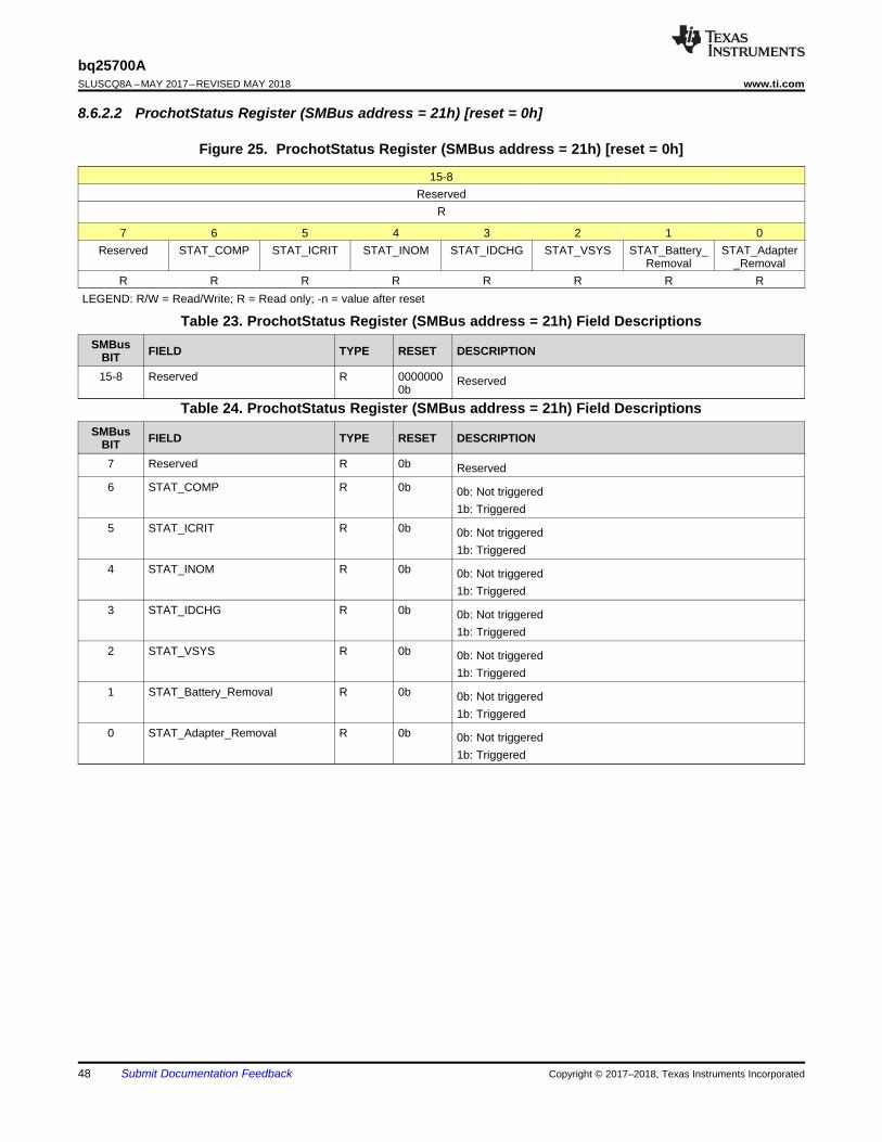
48
bq25700ASLUSCQ8A –MAY 2017–REVISED MAY 2018 www.ti.com
Submit Documentation Feedback Copyright © 2017–2018, Texas Instruments Incorporated
8.6.2.2 ProchotStatus Register (SMBus address = 21h) [reset = 0h]
Figure 25. ProchotStatus Register (SMBus address = 21h) [reset = 0h]
15-8Reserved
R
7 6 5 4 3 2 1 0Reserved STAT_COMP STAT_ICRIT STAT_INOM STAT_IDCHG STAT_VSYS STAT_Battery_
RemovalSTAT_Adapter
_RemovalR R R R R R R R
LEGEND: R/W = Read/Write; R = Read only; -n = value after reset
Table 23. ProchotStatus Register (SMBus address = 21h) Field DescriptionsSMBus
BIT FIELD TYPE RESET DESCRIPTION
15-8 Reserved R 00000000b
Reserved
Table 24. ProchotStatus Register (SMBus address = 21h) Field DescriptionsSMBus
BIT FIELD TYPE RESET DESCRIPTION
7 Reserved R 0b Reserved6 STAT_COMP R 0b 0b: Not triggered
1b: Triggered5 STAT_ICRIT R 0b 0b: Not triggered
1b: Triggered4 STAT_INOM R 0b 0b: Not triggered
1b: Triggered3 STAT_IDCHG R 0b 0b: Not triggered
1b: Triggered2 STAT_VSYS R 0b 0b: Not triggered
1b: Triggered1 STAT_Battery_Removal R 0b 0b: Not triggered
1b: Triggered0 STAT_Adapter_Removal R 0b 0b: Not triggered
1b: Triggered
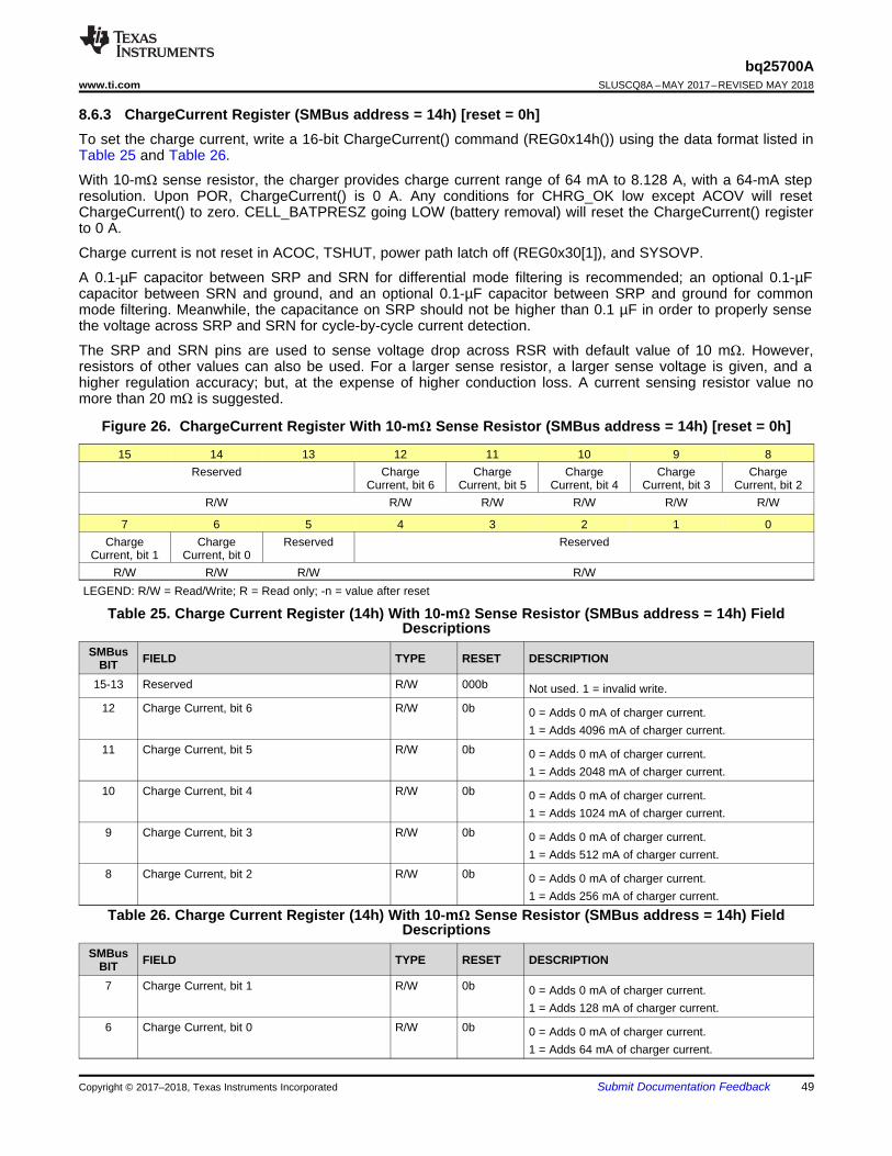
49
bq25700Awww.ti.com SLUSCQ8A –MAY 2017–REVISED MAY 2018
Submit Documentation FeedbackCopyright © 2017–2018, Texas Instruments Incorporated
8.6.3 ChargeCurrent Register (SMBus address = 14h) [reset = 0h]To set the charge current, write a 16-bit ChargeCurrent() command (REG0x14h()) using the data format listed inTable 25 and Table 26.
With 10-mΩ sense resistor, the charger provides charge current range of 64 mA to 8.128 A, with a 64-mA stepresolution. Upon POR, ChargeCurrent() is 0 A. Any conditions for CHRG_OK low except ACOV will resetChargeCurrent() to zero. CELL_BATPRESZ going LOW (battery removal) will reset the ChargeCurrent() registerto 0 A.
Charge current is not reset in ACOC, TSHUT, power path latch off (REG0x30[1]), and SYSOVP.
A 0.1-µF capacitor between SRP and SRN for differential mode filtering is recommended; an optional 0.1-µFcapacitor between SRN and ground, and an optional 0.1-µF capacitor between SRP and ground for commonmode filtering. Meanwhile, the capacitance on SRP should not be higher than 0.1 µF in order to properly sensethe voltage across SRP and SRN for cycle-by-cycle current detection.
The SRP and SRN pins are used to sense voltage drop across RSR with default value of 10 mΩ. However,resistors of other values can also be used. For a larger sense resistor, a larger sense voltage is given, and ahigher regulation accuracy; but, at the expense of higher conduction loss. A current sensing resistor value nomore than 20 mΩ is suggested.
Figure 26. ChargeCurrent Register With 10-mΩ Sense Resistor (SMBus address = 14h) [reset = 0h]
15 14 13 12 11 10 9 8Reserved Charge
Current, bit 6Charge
Current, bit 5Charge
Current, bit 4Charge
Current, bit 3Charge
Current, bit 2R/W R/W R/W R/W R/W R/W
7 6 5 4 3 2 1 0Charge
Current, bit 1Charge
Current, bit 0Reserved Reserved
R/W R/W R/W R/WLEGEND: R/W = Read/Write; R = Read only; -n = value after reset
Table 25. Charge Current Register (14h) With 10-mΩ Sense Resistor (SMBus address = 14h) FieldDescriptions
SMBusBIT FIELD TYPE RESET DESCRIPTION
15-13 Reserved R/W 000b Not used. 1 = invalid write.12 Charge Current, bit 6 R/W 0b 0 = Adds 0 mA of charger current.
1 = Adds 4096 mA of charger current.11 Charge Current, bit 5 R/W 0b 0 = Adds 0 mA of charger current.
1 = Adds 2048 mA of charger current.10 Charge Current, bit 4 R/W 0b 0 = Adds 0 mA of charger current.
1 = Adds 1024 mA of charger current.9 Charge Current, bit 3 R/W 0b 0 = Adds 0 mA of charger current.
1 = Adds 512 mA of charger current.8 Charge Current, bit 2 R/W 0b 0 = Adds 0 mA of charger current.
1 = Adds 256 mA of charger current.
Table 26. Charge Current Register (14h) With 10-mΩ Sense Resistor (SMBus address = 14h) FieldDescriptions
SMBusBIT FIELD TYPE RESET DESCRIPTION
7 Charge Current, bit 1 R/W 0b 0 = Adds 0 mA of charger current.1 = Adds 128 mA of charger current.
6 Charge Current, bit 0 R/W 0b 0 = Adds 0 mA of charger current.1 = Adds 64 mA of charger current.
50
bq25700ASLUSCQ8A –MAY 2017–REVISED MAY 2018 www.ti.com
Submit Documentation Feedback Copyright © 2017–2018, Texas Instruments Incorporated
Table 26. Charge Current Register (14h) With 10-mΩ Sense Resistor (SMBus address = 14h) FieldDescriptions (continued)
SMBusBIT FIELD TYPE RESET DESCRIPTION
5-0 Reserved R/W 000000b Not used. Value Ignored.
8.6.3.1 Battery Pre-Charge Current ClampDuring pre-charge, BATFET works in linear mode or LDO mode (default REG0x12[2] = 1). For 2-4 cell battery,the system is regulated at minimum system voltage in REG0x3E() and the pre-charge current is clamped at 384mA. For 1 cell battery, the pre-charge to fast charge threshold is 3 V, and the pre-charge current is clamped at384 mA. However, the BATFET stays in LDO mode operation till battery voltage is above minimum systemvoltage (~3.6 V). During battery voltage from 3 V to 3.6 V, the fast charge current is clamped at 2 A.
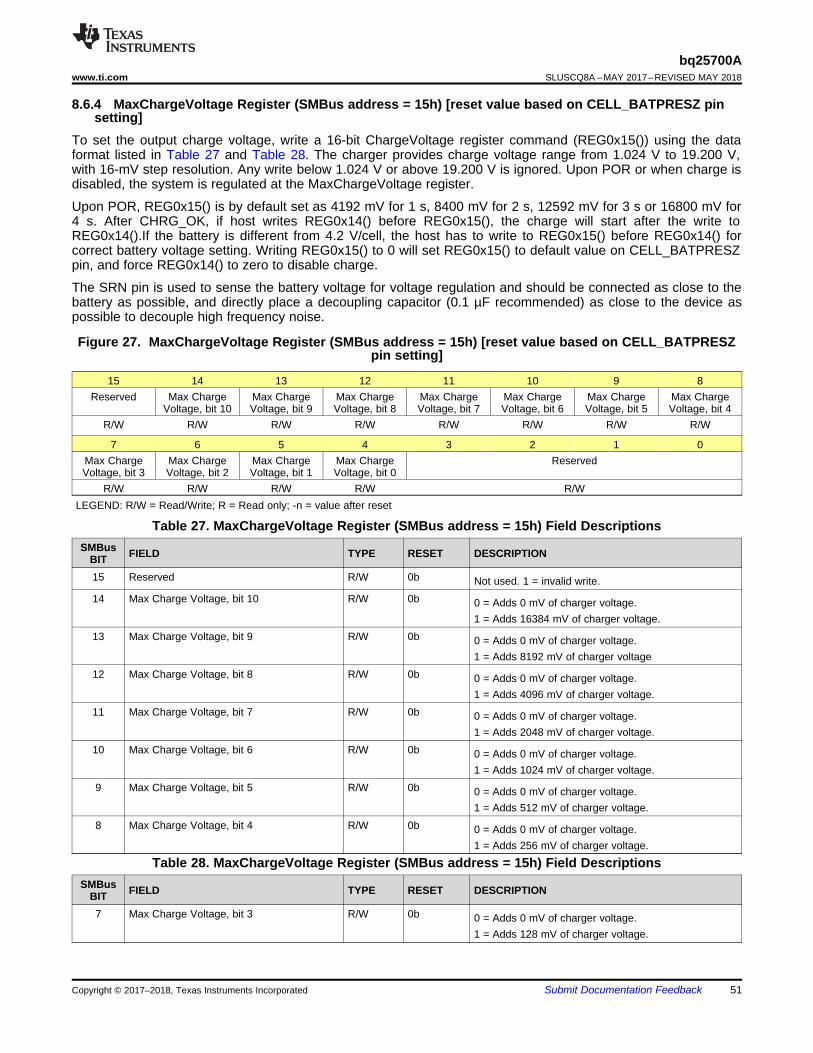
51
bq25700Awww.ti.com SLUSCQ8A –MAY 2017–REVISED MAY 2018
Submit Documentation FeedbackCopyright © 2017–2018, Texas Instruments Incorporated
8.6.4 MaxChargeVoltage Register (SMBus address = 15h) [reset value based on CELL_BATPRESZ pinsetting]
To set the output charge voltage, write a 16-bit ChargeVoltage register command (REG0x15()) using the dataformat listed in Table 27 and Table 28. The charger provides charge voltage range from 1.024 V to 19.200 V,with 16-mV step resolution. Any write below 1.024 V or above 19.200 V is ignored. Upon POR or when charge isdisabled, the system is regulated at the MaxChargeVoltage register.
Upon POR, REG0x15() is by default set as 4192 mV for 1 s, 8400 mV for 2 s, 12592 mV for 3 s or 16800 mV for4 s. After CHRG_OK, if host writes REG0x14() before REG0x15(), the charge will start after the write toREG0x14().If the battery is different from 4.2 V/cell, the host has to write to REG0x15() before REG0x14() forcorrect battery voltage setting. Writing REG0x15() to 0 will set REG0x15() to default value on CELL_BATPRESZpin, and force REG0x14() to zero to disable charge.
The SRN pin is used to sense the battery voltage for voltage regulation and should be connected as close to thebattery as possible, and directly place a decoupling capacitor (0.1 µF recommended) as close to the device aspossible to decouple high frequency noise.
Figure 27. MaxChargeVoltage Register (SMBus address = 15h) [reset value based on CELL_BATPRESZpin setting]
15 14 13 12 11 10 9 8Reserved Max Charge
Voltage, bit 10Max ChargeVoltage, bit 9
Max ChargeVoltage, bit 8
Max ChargeVoltage, bit 7
Max ChargeVoltage, bit 6
Max ChargeVoltage, bit 5
Max ChargeVoltage, bit 4
R/W R/W R/W R/W R/W R/W R/W R/W
7 6 5 4 3 2 1 0Max ChargeVoltage, bit 3
Max ChargeVoltage, bit 2
Max ChargeVoltage, bit 1
Max ChargeVoltage, bit 0
Reserved
R/W R/W R/W R/W R/WLEGEND: R/W = Read/Write; R = Read only; -n = value after reset
Table 27. MaxChargeVoltage Register (SMBus address = 15h) Field DescriptionsSMBus
BIT FIELD TYPE RESET DESCRIPTION
15 Reserved R/W 0b Not used. 1 = invalid write.14 Max Charge Voltage, bit 10 R/W 0b 0 = Adds 0 mV of charger voltage.
1 = Adds 16384 mV of charger voltage.13 Max Charge Voltage, bit 9 R/W 0b 0 = Adds 0 mV of charger voltage.
1 = Adds 8192 mV of charger voltage12 Max Charge Voltage, bit 8 R/W 0b 0 = Adds 0 mV of charger voltage.
1 = Adds 4096 mV of charger voltage.11 Max Charge Voltage, bit 7 R/W 0b 0 = Adds 0 mV of charger voltage.
1 = Adds 2048 mV of charger voltage.10 Max Charge Voltage, bit 6 R/W 0b 0 = Adds 0 mV of charger voltage.
1 = Adds 1024 mV of charger voltage.9 Max Charge Voltage, bit 5 R/W 0b 0 = Adds 0 mV of charger voltage.
1 = Adds 512 mV of charger voltage.8 Max Charge Voltage, bit 4 R/W 0b 0 = Adds 0 mV of charger voltage.
1 = Adds 256 mV of charger voltage.
Table 28. MaxChargeVoltage Register (SMBus address = 15h) Field DescriptionsSMBus
BIT FIELD TYPE RESET DESCRIPTION
7 Max Charge Voltage, bit 3 R/W 0b 0 = Adds 0 mV of charger voltage.1 = Adds 128 mV of charger voltage.
52
bq25700ASLUSCQ8A –MAY 2017–REVISED MAY 2018 www.ti.com
Submit Documentation Feedback Copyright © 2017–2018, Texas Instruments Incorporated
Table 28. MaxChargeVoltage Register (SMBus address = 15h) Field Descriptions (continued)SMBus
BIT FIELD TYPE RESET DESCRIPTION
6 Max Charge Voltage, bit 2 R/W 0b 0 = Adds 0 mV of charger voltage.1 = Adds 64 mV of charger voltage.
5 Max Charge Voltage, bit 1 R/W 0b 0 = Adds 0 mV of charger voltage.1 = Adds 32 mV of charger voltage.
4 Max Charge Voltage, bit 0 R/W 0b 0 = Adds 0 mV of charger voltage.1 = Adds 16 mV of charger voltage.
3-0 Reserved R/W 0000b Not used. Value Ignored.
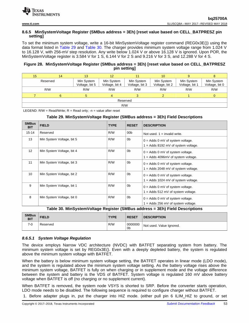
53
bq25700Awww.ti.com SLUSCQ8A –MAY 2017–REVISED MAY 2018
Submit Documentation FeedbackCopyright © 2017–2018, Texas Instruments Incorporated
8.6.5 MinSystemVoltage Register (SMBus address = 3Eh) [reset value based on CELL_BATPRESZ pinsetting]
To set the minimum system voltage, write a 16-bit MinSystemVoltage register command (REG0x3E()) using thedata format listed in Table 29 and Table 30. The charger provides minimum system voltage range from 1.024 Vto 16.128 V, with 256-mV step resolution. Any write below 1.024 V or above 16.128 V is ignored. Upon POR, theMinSystemVoltage register is 3.584 V for 1 S, 6.144 V for 2 S and 9.216 V for 3 S, and 12.288 V for 4 S.
Figure 28. MinSystemVoltage Register (SMBus address = 3Eh) [reset value based on CELL_BATPRESZpin setting]
15 14 13 12 11 10 9 8Reserved Min System
Voltage, bit 5Min System
Voltage, bit 4Min System
Voltage, bit 3Min System
Voltage, bit 2Min System
Voltage, bit 1Min System
Voltage, bit 0R/W R/W R/W R/W R/W R/W R/W
7 6 5 4 3 2 1 0Reserved
R/WLEGEND: R/W = Read/Write; R = Read only; -n = value after reset
Table 29. MinSystemVoltage Register (SMBus address = 3Eh) Field DescriptionsSMBus
BIT FIELD TYPE RESET DESCRIPTION
15-14 Reserved R/W 00b Not used. 1 = invalid write.13 Min System Voltage, bit 5 R/W 0b 0 = Adds 0 mV of system voltage.
1 = Adds 8192 mV of system voltage.12 Min System Voltage, bit 4 R/W 0b 0 = Adds 0 mV of system voltage.
1 = Adds 4096mV of system voltage.11 Min System Voltage, bit 3 R/W 0b 0 = Adds 0 mV of system voltage.
1 = Adds 2048 mV of system voltage.10 Min System Voltage, bit 2 R/W 0b 0 = Adds 0 mV of system voltage.
1 = Adds 1024 mV of system voltage.9 Min System Voltage, bit 1 R/W 0b 0 = Adds 0 mV of system voltage.
1 = Adds 512 mV of system voltage.8 Min System Voltage, bit 0 R/W 0b 0 = Adds 0 mV of system voltage.
1 = Adds 256 mV of system voltage.
Table 30. MinSystemVoltage Register (SMBus address = 3Eh) Field DescriptionsSMBus
BIT FIELD TYPE RESET DESCRIPTION
7-0 Reserved R/W 00000000b
Not used. Value Ignored.
8.6.5.1 System Voltage RegulationThe device employs Narrow VDC architecture (NVDC) with BATFET separating system from battery. Theminimum system voltage is set by REG0x3E(). Even with a deeply depleted battery, the system is regulatedabove the minimum system voltage with BATFET.
When the battery is below minimum system voltage setting, the BATFET operates in linear mode (LDO mode),and the system is regulated above the minimum system voltage setting. As the battery voltage rises above theminimum system voltage, BATFET is fully on when charging or in supplement mode and the voltage differencebetween the system and battery is the VDS of BATFET. System voltage is regulated 160 mV above batteryvoltage when BATFET is off (no charging or no supplement current).
When BATFET is removed, the system node VSYS is shorted to SRP. Before the converter starts operation,LDO mode needs to be disabled. The following sequence is required to configure charger without BATFET.1. Before adapter plugs in, put the charger into HIZ mode. (either pull pin 6 ILIM_HIZ to ground, or set
( )ILIM_HIZ ACP ACN DPM ACV 1V 40 V V 1 40 I R= + ´ - = + ´ ´
54
bq25700ASLUSCQ8A –MAY 2017–REVISED MAY 2018 www.ti.com
Submit Documentation Feedback Copyright © 2017–2018, Texas Instruments Incorporated
REG0x32[15] to 1)2. Set 0x12[2] to 0 to disable LDO mode.3. Set 0x30[0] to 0 to disable auto-wakeup mode.4. Check if battery voltage is properly programmed (REG0x15)5. Set pre-charge/charge current (REG0x14)6. Put the device out of HIZ mode. (Release ILIM_HIZ from ground and set REG0x32[15]=0).
In order to prevent any accidental SW mistakes, the host sets low input current limit (a few hundred milliamps)when device is out of HIZ.
8.6.6 Input Current and Input Voltage Registers for Dynamic Power ManagementThe charger supports Dynamic Power Management (DPM). Normally, the input power source provides power forthe system load or to charge the battery. When the input current exceeds the input current setting, or the inputvoltage falls below the input voltage setting, the charger decreases the charge current to provide priority to thesystem load. As the system current rises, the available charge current drops accordingly towards zero. If thesystem load keeps increasing after the charge current drops down to zero, the system voltage starts to drop. Asthe system voltage drops below the battery voltage, the battery will discharge to supply the heavy system load.
8.6.6.1 Input Current RegistersTo set the maximum input current limit, write a 16-bit IIN_HOST register command (REG0x3F()) using the dataformat listed in Table 31 and Table 32. When using a 10-mΩ sense resistor, the charger provides an input-current limit range of 50 mA to 6400 mA, with 50-mA resolution. The default current limit is 3.3 A. Due to theUSB current setting requirement, the register setting specifies the maximum current instead of the typical current.Upon adapter removal, the input current limit is reset to the default value of 3.3 A. The register offset is 50 mA.With code 0, the input current limit is 50 mA.
The ACP and ACN pins are used to sense RAC with the default value of 10 mΩ. For a 20-mΩ sense resistor, alarger sense voltage is given and a higher regulation accuracy, but at the expense of higher conduction loss.
Instead of using the internal DPM loop, the user can build up an external input current regulation loop and havethe feedback signal on the ILIM_HIZ pin.
(2)
In order to disable ILIM_HIZ pin, the host can write to 0x31[7] to disable ILIM_HIZ pin, or pull ILIM_HIZ pin above4.0 V.
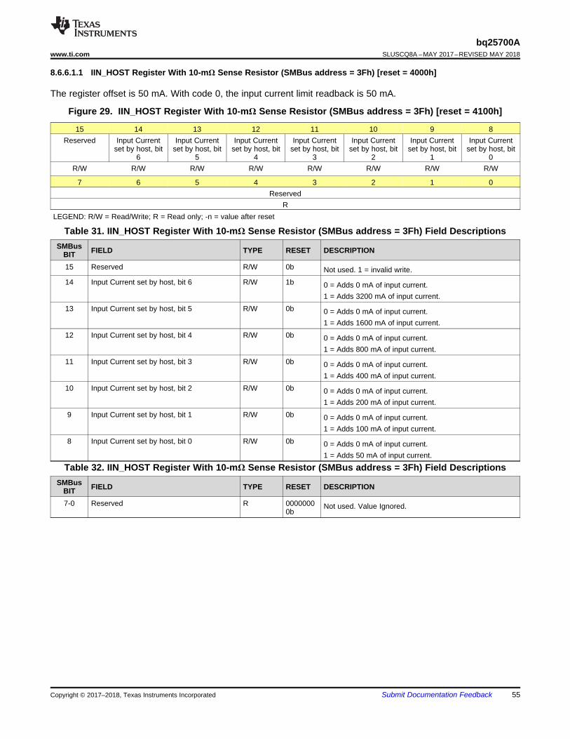
55
bq25700Awww.ti.com SLUSCQ8A –MAY 2017–REVISED MAY 2018
Submit Documentation FeedbackCopyright © 2017–2018, Texas Instruments Incorporated
8.6.6.1.1 IIN_HOST Register With 10-mΩ Sense Resistor (SMBus address = 3Fh) [reset = 4000h]
The register offset is 50 mA. With code 0, the input current limit readback is 50 mA.
Figure 29. IIN_HOST Register With 10-mΩ Sense Resistor (SMBus address = 3Fh) [reset = 4100h]
15 14 13 12 11 10 9 8Reserved Input Current
set by host, bit6
Input Currentset by host, bit
5
Input Currentset by host, bit
4
Input Currentset by host, bit
3
Input Currentset by host, bit
2
Input Currentset by host, bit
1
Input Currentset by host, bit
0R/W R/W R/W R/W R/W R/W R/W R/W
7 6 5 4 3 2 1 0Reserved
RLEGEND: R/W = Read/Write; R = Read only; -n = value after reset
Table 31. IIN_HOST Register With 10-mΩ Sense Resistor (SMBus address = 3Fh) Field DescriptionsSMBus
BIT FIELD TYPE RESET DESCRIPTION
15 Reserved R/W 0b Not used. 1 = invalid write.14 Input Current set by host, bit 6 R/W 1b 0 = Adds 0 mA of input current.
1 = Adds 3200 mA of input current.13 Input Current set by host, bit 5 R/W 0b 0 = Adds 0 mA of input current.
1 = Adds 1600 mA of input current.12 Input Current set by host, bit 4 R/W 0b 0 = Adds 0 mA of input current.
1 = Adds 800 mA of input current.11 Input Current set by host, bit 3 R/W 0b 0 = Adds 0 mA of input current.
1 = Adds 400 mA of input current.10 Input Current set by host, bit 2 R/W 0b 0 = Adds 0 mA of input current.
1 = Adds 200 mA of input current.9 Input Current set by host, bit 1 R/W 0b 0 = Adds 0 mA of input current.
1 = Adds 100 mA of input current.8 Input Current set by host, bit 0 R/W 0b 0 = Adds 0 mA of input current.
1 = Adds 50 mA of input current.
Table 32. IIN_HOST Register With 10-mΩ Sense Resistor (SMBus address = 3Fh) Field DescriptionsSMBus
BIT FIELD TYPE RESET DESCRIPTION
7-0 Reserved R 00000000b
Not used. Value Ignored.
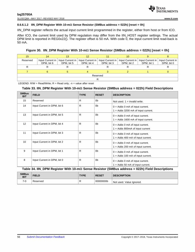
56
bq25700ASLUSCQ8A –MAY 2017–REVISED MAY 2018 www.ti.com
Submit Documentation Feedback Copyright © 2017–2018, Texas Instruments Incorporated
8.6.6.1.2 IIN_DPM Register With 10-mΩ Sense Resistor (SMBus address = 022h) [reset = 0h]
IIN_DPM register reflects the actual input current limit programmed in the register, either from host or from ICO.
After ICO, the current limit used by DPM regulation may differ from the IIN_HOST register settings. The actualDPM limit is reported in REG0x22(). The register offset is 50 mA. With code 0, the input current limit read-back is50 mA.
Figure 30. IIN_DPM Register With 10-mΩ Sense Resistor (SMBus address = 022h) [reset = 0h]
15 14 13 12 11 10 9 8Reserved Input Current in
DPM, bit 6Input Current in
DPM, bit 5Input Current in
DPM, bit 4Input Current in
DPM, bit 3Input Current in
DPM, bit 2Input Current in
DPM, bit 1Input Current in
DPM, bit 0R R R R R R R R
7 6 5 4 3 2 1 0Reserved
RLEGEND: R/W = Read/Write; R = Read only; -n = value after reset
Table 33. IIN_DPM Register With 10-mΩ Sense Resistor (SMBus address = 022h) Field DescriptionsSMBus
BIT FIELD TYPE RESET DESCRIPTION
15 Reserved R 0b Not used. 1 = invalid write.14 Input Current in DPM, bit 6 R 0b 0 = Adds 0 mA of input current.
1 = Adds 3200 mA of input current.13 Input Current in DPM, bit 5 R 0b 0 = Adds 0 mA of input current.
1 = Adds 1600 mA of input current.12 Input Current in DPM, bit 4 R 0b 0 = Adds 0 mA of input current.
1 = Adds 800mA of input current11 Input Current in DPM, bit 3 R 0b 0 = Adds 0 mA of input current.
1 = Adds 400 mA of input current.10 Input Current in DPM, bit 2 R 0b 0 = Adds 0 mA of input current.
1 = Adds 200 mA of input current.9 Input Current in DPM, bit 1 R 0b 0 = Adds 0 mA of input current.
1 = Adds 100 mA of input current.8 Input Current in DPM, bit 0 R 0b 0 = Adds 0 mA of input current.
1 = Adds 50 mA of input current.
Table 34. IIN_DPM Register With 10-mΩ Sense Resistor (SMBus address = 022h) Field DescriptionsSMBus
BIT FIELD TYPE RESET DESCRIPTION
7-0 Reserved R 00000000b Not used. Value Ignored.
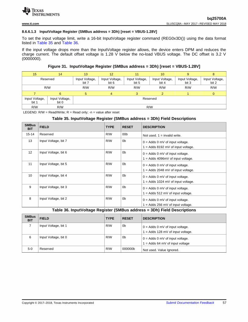
57
bq25700Awww.ti.com SLUSCQ8A –MAY 2017–REVISED MAY 2018
Submit Documentation FeedbackCopyright © 2017–2018, Texas Instruments Incorporated
8.6.6.1.3 InputVoltage Register (SMBus address = 3Dh) [reset = VBUS-1.28V]
To set the input voltage limit, write a 16-bit InputVoltage register command (REG0x3D()) using the data formatlisted in Table 35 and Table 36.
If the input voltage drops more than the InputVoltage register allows, the device enters DPM and reduces thecharge current. The default offset voltage is 1.28 V below the no-load VBUS voltage. The DC offset is 3.2 V(0000000).
Figure 31. InputVoltage Register (SMBus address = 3Dh) [reset = VBUS-1.28V]
15 14 13 12 11 10 9 8Reserved Input Voltage,
bit 7Input Voltage,
bit 6Input Voltage,
bit 5Input Voltage,
bit 4Input Voltage,
bit 3Input Voltage,
bit 2R/W R/W R/W R/W R/W R/W R/W
7 6 5 4 3 2 1 0Input Voltage,
bit 1Input Voltage,
bit 0Reserved
R/W R/W R/WLEGEND: R/W = Read/Write; R = Read only; -n = value after reset
Table 35. InputVoltage Register (SMBus address = 3Dh) Field DescriptionsSMBus
BIT FIELD TYPE RESET DESCRIPTION
15-14 Reserved R/W 00b Not used. 1 = invalid write.13 Input Voltage, bit 7 R/W 0b 0 = Adds 0 mV of input voltage.
1 = Adds 8192 mV of input voltage.12 Input Voltage, bit 6 R/W 0b 0 = Adds 0 mV of input voltage.
1 = Adds 4096mV of input voltage.11 Input Voltage, bit 5 R/W 0b 0 = Adds 0 mV of input voltage.
1 = Adds 2048 mV of input voltage.10 Input Voltage, bit 4 R/W 0b 0 = Adds 0 mV of input voltage.
1 = Adds 1024 mV of input voltage.9 Input Voltage, bit 3 R/W 0b 0 = Adds 0 mV of input voltage.
1 = Adds 512 mV of input voltage.8 Input Voltage, bit 2 R/W 0b 0 = Adds 0 mV of input voltage.
1 = Adds 256 mV of input voltage.
Table 36. InputVoltage Register (SMBus address = 3Dh) Field DescriptionsSMBus
BIT FIELD TYPE RESET DESCRIPTION
7 Input Voltage, bit 1 R/W 0b 0 = Adds 0 mV of input voltage.1 = Adds 128 mV of input voltage.
6 Input Voltage, bit 0 R/W 0b 0 = Adds 0 mV of input voltage.1 = Adds 64 mV of input voltage
5-0 Reserved R/W 000000b Not used. Value Ignored.
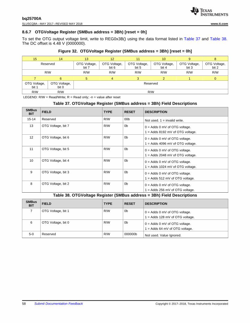
58
bq25700ASLUSCQ8A –MAY 2017–REVISED MAY 2018 www.ti.com
Submit Documentation Feedback Copyright © 2017–2018, Texas Instruments Incorporated
8.6.7 OTGVoltage Register (SMBus address = 3Bh) [reset = 0h]To set the OTG output voltage limit, write to REG0x3B() using the data format listed in Table 37 and Table 38.The DC offset is 4.48 V (0000000).
Figure 32. OTGVoltage Register (SMBus address = 3Bh) [reset = 0h]
15 14 13 12 11 10 9 8Reserved OTG Voltage,
bit 7OTG Voltage,
bit 6OTG Voltage,
bit 5OTG Voltage,
bit 4OTG Voltage,
bit 3OTG Voltage,
bit 2R/W R/W R/W R/W R/W R/W R/W
7 6 5 4 3 2 1 0OTG Voltage,
bit 1OTG Voltage,
bit 0Reserved
R/W R/W R/WLEGEND: R/W = Read/Write; R = Read only; -n = value after reset
Table 37. OTGVoltage Register (SMBus address = 3Bh) Field DescriptionsSMBus
BIT FIELD TYPE RESET DESCRIPTION
15-14 Reserved R/W 00b Not used. 1 = invalid write.13 OTG Voltage, bit 7 R/W 0b 0 = Adds 0 mV of OTG voltage.
1 = Adds 8192 mV of OTG voltage.12 OTG Voltage, bit 6 R/W 0b 0 = Adds 0 mV of OTG voltage.
1 = Adds 4096 mV of OTG voltage.11 OTG Voltage, bit 5 R/W 0b 0 = Adds 0 mV of OTG voltage.
1 = Adds 2048 mV of OTG voltage.10 OTG Voltage, bit 4 R/W 0b 0 = Adds 0 mV of OTG voltage.
1 = Adds 1024 mV of OTG voltage.9 OTG Voltage, bit 3 R/W 0b 0 = Adds 0 mV of OTG voltage.
1 = Adds 512 mV of OTG voltage.8 OTG Voltage, bit 2 R/W 0b 0 = Adds 0 mV of OTG voltage.
1 = Adds 256 mV of OTG voltage.
Table 38. OTGVoltage Register (SMBus address = 3Bh) Field DescriptionsSMBus
BIT FIELD TYPE RESET DESCRIPTION
7 OTG Voltage, bit 1 R/W 0b 0 = Adds 0 mV of OTG voltage.1 = Adds 128 mV of OTG voltage.
6 OTG Voltage, bit 0 R/W 0b 0 = Adds 0 mV of OTG voltage.1 = Adds 64 mV of OTG voltage.
5-0 Reserved R/W 000000b Not used. Value Ignored.
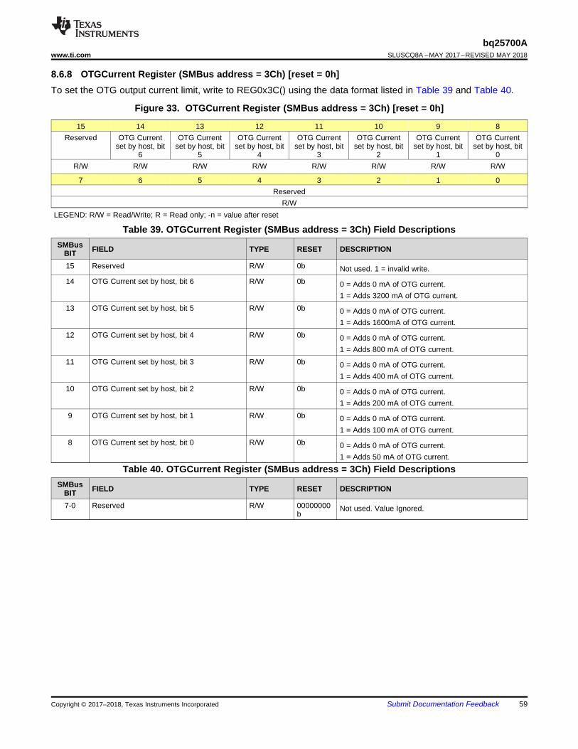
59
bq25700Awww.ti.com SLUSCQ8A –MAY 2017–REVISED MAY 2018
Submit Documentation FeedbackCopyright © 2017–2018, Texas Instruments Incorporated
8.6.8 OTGCurrent Register (SMBus address = 3Ch) [reset = 0h]To set the OTG output current limit, write to REG0x3C() using the data format listed in Table 39 and Table 40.
Figure 33. OTGCurrent Register (SMBus address = 3Ch) [reset = 0h]
15 14 13 12 11 10 9 8Reserved OTG Current
set by host, bit6
OTG Currentset by host, bit
5
OTG Currentset by host, bit
4
OTG Currentset by host, bit
3
OTG Currentset by host, bit
2
OTG Currentset by host, bit
1
OTG Currentset by host, bit
0R/W R/W R/W R/W R/W R/W R/W R/W
7 6 5 4 3 2 1 0Reserved
R/WLEGEND: R/W = Read/Write; R = Read only; -n = value after reset
Table 39. OTGCurrent Register (SMBus address = 3Ch) Field DescriptionsSMBus
BIT FIELD TYPE RESET DESCRIPTION
15 Reserved R/W 0b Not used. 1 = invalid write.14 OTG Current set by host, bit 6 R/W 0b 0 = Adds 0 mA of OTG current.
1 = Adds 3200 mA of OTG current.13 OTG Current set by host, bit 5 R/W 0b 0 = Adds 0 mA of OTG current.
1 = Adds 1600mA of OTG current.12 OTG Current set by host, bit 4 R/W 0b 0 = Adds 0 mA of OTG current.
1 = Adds 800 mA of OTG current.11 OTG Current set by host, bit 3 R/W 0b 0 = Adds 0 mA of OTG current.
1 = Adds 400 mA of OTG current.10 OTG Current set by host, bit 2 R/W 0b 0 = Adds 0 mA of OTG current.
1 = Adds 200 mA of OTG current.9 OTG Current set by host, bit 1 R/W 0b 0 = Adds 0 mA of OTG current.
1 = Adds 100 mA of OTG current.8 OTG Current set by host, bit 0 R/W 0b 0 = Adds 0 mA of OTG current.
1 = Adds 50 mA of OTG current.
Table 40. OTGCurrent Register (SMBus address = 3Ch) Field DescriptionsSMBus
BIT FIELD TYPE RESET DESCRIPTION
7-0 Reserved R/W 00000000b
Not used. Value Ignored.
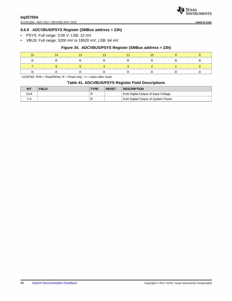
60
bq25700ASLUSCQ8A –MAY 2017–REVISED MAY 2018 www.ti.com
Submit Documentation Feedback Copyright © 2017–2018, Texas Instruments Incorporated
8.6.9 ADCVBUS/PSYS Register (SMBus address = 23h)• PSYS: Full range: 3.06 V, LSB: 12 mV• VBUS: Full range: 3200 mV to 19520 mV, LSB: 64 mV
Figure 34. ADCVBUS/PSYS Register (SMBus address = 23h)
15 14 13 12 11 10 9 8
R R R R R R R R
7 6 5 4 3 2 1 0
R R R R R R R RLEGEND: R/W = Read/Write; R = Read only; -n = value after reset
Table 41. ADCVBUS/PSYS Register Field DescriptionsBIT FIELD TYPE RESET DESCRIPTION15-8 R 8-bit Digital Output of Input Voltage7-0 R 8-bit Digital Output of System Power
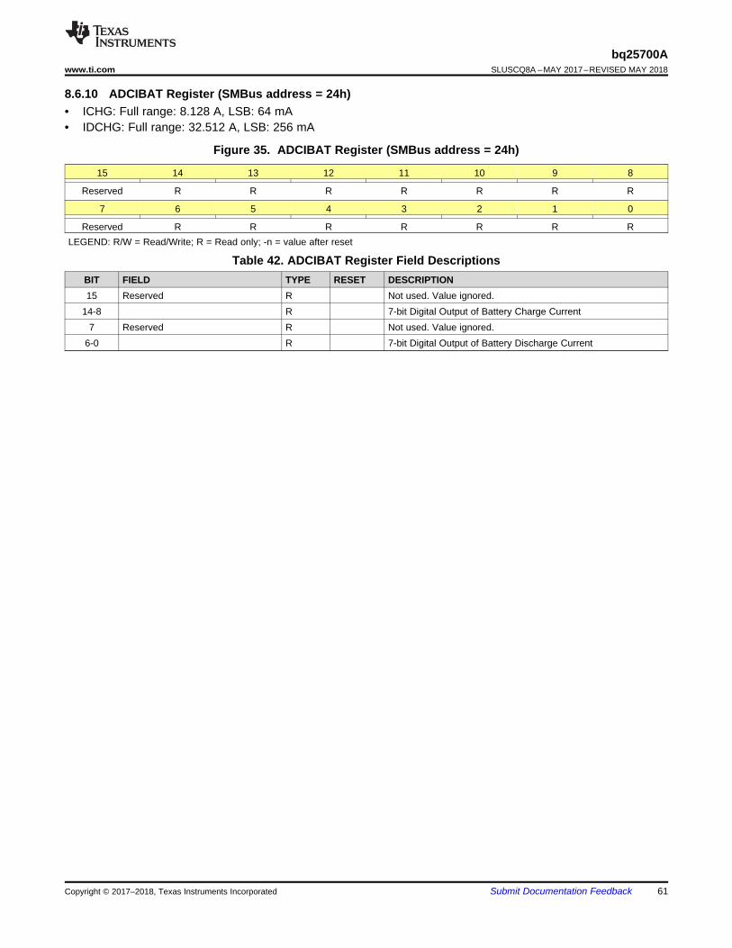
61
bq25700Awww.ti.com SLUSCQ8A –MAY 2017–REVISED MAY 2018
Submit Documentation FeedbackCopyright © 2017–2018, Texas Instruments Incorporated
8.6.10 ADCIBAT Register (SMBus address = 24h)• ICHG: Full range: 8.128 A, LSB: 64 mA• IDCHG: Full range: 32.512 A, LSB: 256 mA
Figure 35. ADCIBAT Register (SMBus address = 24h)
15 14 13 12 11 10 9 8
Reserved R R R R R R R
7 6 5 4 3 2 1 0
Reserved R R R R R R RLEGEND: R/W = Read/Write; R = Read only; -n = value after reset
Table 42. ADCIBAT Register Field DescriptionsBIT FIELD TYPE RESET DESCRIPTION15 Reserved R Not used. Value ignored.
14-8 R 7-bit Digital Output of Battery Charge Current7 Reserved R Not used. Value ignored.
6-0 R 7-bit Digital Output of Battery Discharge Current
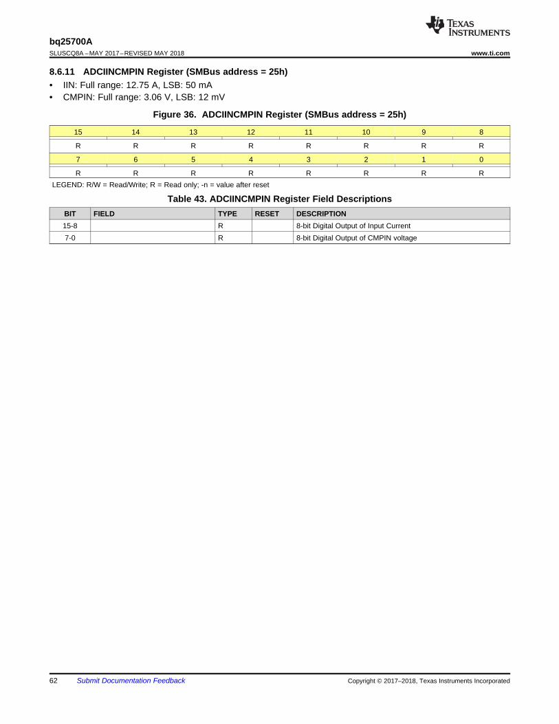
62
bq25700ASLUSCQ8A –MAY 2017–REVISED MAY 2018 www.ti.com
Submit Documentation Feedback Copyright © 2017–2018, Texas Instruments Incorporated
8.6.11 ADCIINCMPIN Register (SMBus address = 25h)• IIN: Full range: 12.75 A, LSB: 50 mA• CMPIN: Full range: 3.06 V, LSB: 12 mV
Figure 36. ADCIINCMPIN Register (SMBus address = 25h)
15 14 13 12 11 10 9 8
R R R R R R R R
7 6 5 4 3 2 1 0
R R R R R R R RLEGEND: R/W = Read/Write; R = Read only; -n = value after reset
Table 43. ADCIINCMPIN Register Field DescriptionsBIT FIELD TYPE RESET DESCRIPTION15-8 R 8-bit Digital Output of Input Current7-0 R 8-bit Digital Output of CMPIN voltage
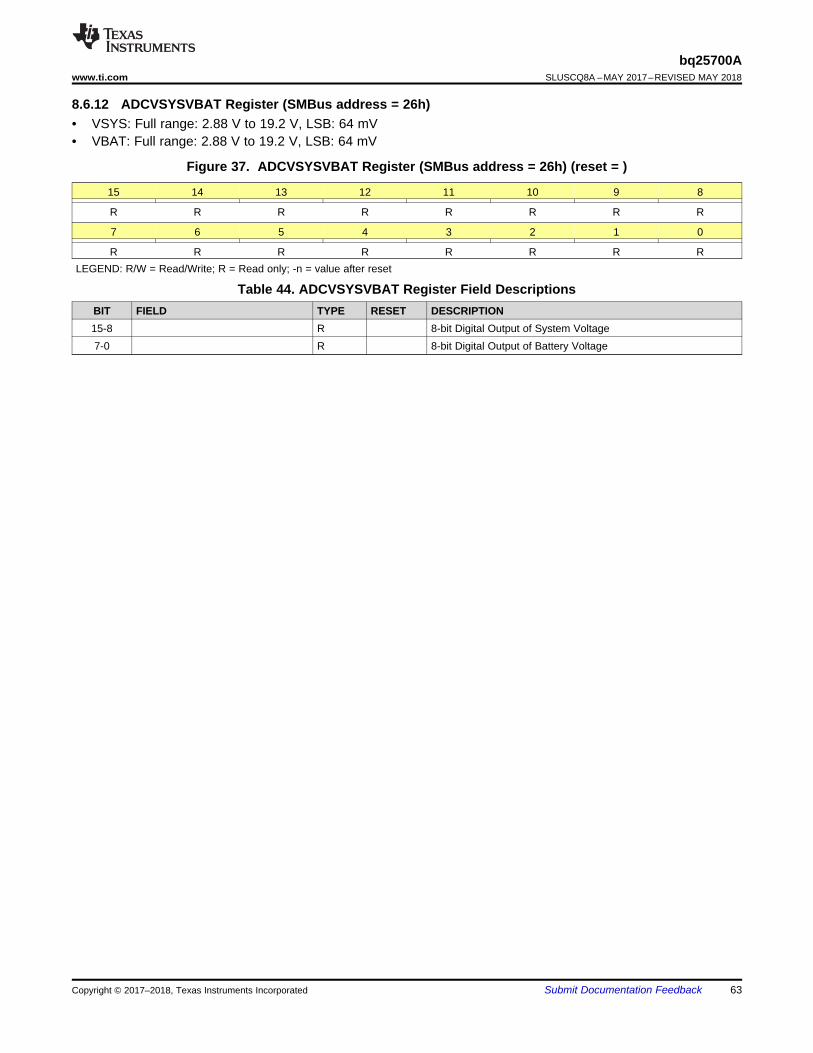
63
bq25700Awww.ti.com SLUSCQ8A –MAY 2017–REVISED MAY 2018
Submit Documentation FeedbackCopyright © 2017–2018, Texas Instruments Incorporated
8.6.12 ADCVSYSVBAT Register (SMBus address = 26h)• VSYS: Full range: 2.88 V to 19.2 V, LSB: 64 mV• VBAT: Full range: 2.88 V to 19.2 V, LSB: 64 mV
Figure 37. ADCVSYSVBAT Register (SMBus address = 26h) (reset = )
15 14 13 12 11 10 9 8
R R R R R R R R
7 6 5 4 3 2 1 0
R R R R R R R RLEGEND: R/W = Read/Write; R = Read only; -n = value after reset
Table 44. ADCVSYSVBAT Register Field DescriptionsBIT FIELD TYPE RESET DESCRIPTION15-8 R 8-bit Digital Output of System Voltage7-0 R 8-bit Digital Output of Battery Voltage
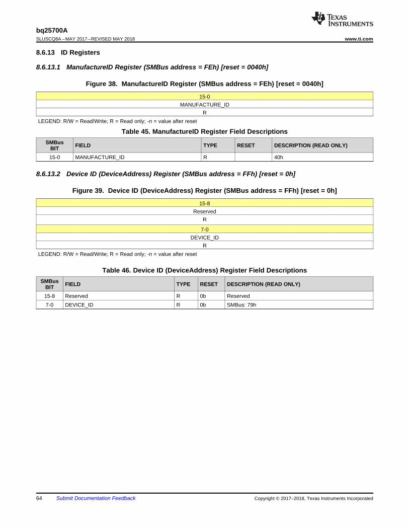
64
bq25700ASLUSCQ8A –MAY 2017–REVISED MAY 2018 www.ti.com
Submit Documentation Feedback Copyright © 2017–2018, Texas Instruments Incorporated
8.6.13 ID Registers
8.6.13.1 ManufactureID Register (SMBus address = FEh) [reset = 0040h]
Figure 38. ManufactureID Register (SMBus address = FEh) [reset = 0040h]
15-0MANUFACTURE_ID
RLEGEND: R/W = Read/Write; R = Read only; -n = value after reset
Table 45. ManufactureID Register Field DescriptionsSMBus
BIT FIELD TYPE RESET DESCRIPTION (READ ONLY)
15-0 MANUFACTURE_ID R 40h
8.6.13.2 Device ID (DeviceAddress) Register (SMBus address = FFh) [reset = 0h]
Figure 39. Device ID (DeviceAddress) Register (SMBus address = FFh) [reset = 0h]
15-8Reserved
R
7-0DEVICE_ID
RLEGEND: R/W = Read/Write; R = Read only; -n = value after reset
Table 46. Device ID (DeviceAddress) Register Field DescriptionsSMBus
BIT FIELD TYPE RESET DESCRIPTION (READ ONLY)
15-8 Reserved R 0b Reserved7-0 DEVICE_ID R 0b SMBus: 79h
bq25700A
ACN
VBUSHIDRV1
SRN
IADPTIBAT
PSYS
ADAPTER
VSYS
BATT
BTST1 BTST2LODRV1
SW1 SW2LODRV2
HIDRV2
SRP
BATDRV
VDDA
COMP1
COMP2
SDA SCL
3.3V or 1.8V
CHRG_OK
CELL_BATPRESZ
1.05V PROCHOT
ACP
SYS
Host(SMBus)
Q1Q2 Q3 Q4
REGN
GND
ILIM_HIZ
EN_OTG
RAC=10m:
2.2±3.3uF1uF
REGN10:
50:
10k:
10k:
10k:
100pF100pF30k:
VDDA
250k:
350k:
To CPU
47nF 47nF
6x10PF���:
1PF
6x10PF
Optional snubber
10k:
CMPOUT
CMPIN
RSR=10m:
10nF
2.2uH
100k:
1:
470nF
15nF 15nF
10: 10:
Copyright © 2017, Texas Instruments Incorporated
65
bq25700Awww.ti.com SLUSCQ8A –MAY 2017–REVISED MAY 2018
Submit Documentation FeedbackCopyright © 2017–2018, Texas Instruments Incorporated
(1) Refer to adapter specification for settings for Input Voltage and Input Current Limit.(2) Refer to battery specification for settings.
9 Application and Implementation
NOTEInformation in the following applications sections is not part of the TI componentspecification, and TI does not warrant its accuracy or completeness. TI’s customers areresponsible for determining suitability of components for their purposes. Customers shouldvalidate and test their design implementation to confirm system functionality.
9.1 Application InformationThe bq2570xEVM-732 evaluation module (EVM) is a complete charger module for evaluating the bq25700A. Theapplication curves were taken using the bq2570xEVM-732. Refer to the EVM user's guide (SLUUBG6) for EVMinformation.
9.2 Typical Application
Figure 40. Application Diagram
9.2.1 Design Requirements
DESIGN PARAMETER EXAMPLE VALUEInput Voltage (1) 3.5 V < Adapter Voltage < 24 V
Input Current Limit (1) 3.2 A for 65 W adapterBattery Charge Voltage (2) 8400 mV for 2s battery
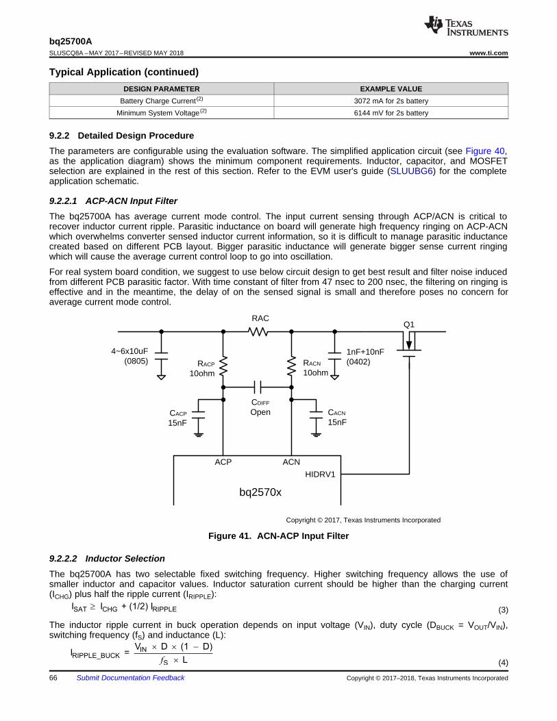
INRIPPLE_BUCK
S
V D (1 D)I =
L
´ ´ -
´f
SAT CHG RIPPLEI I + (1/2) I³
RAC
ACP ACN
RACP
10ohmRACN
10ohm
CACP
15nFCACN
15nF
bq2570x
CDIFF
Open
4~6x10uF(0805)
1nF+10nF(0402)
HIDRV1
Q1
Copyright © 2017, Texas Instruments Incorporated
66
bq25700ASLUSCQ8A –MAY 2017–REVISED MAY 2018 www.ti.com
Submit Documentation Feedback Copyright © 2017–2018, Texas Instruments Incorporated
Typical Application (continued)DESIGN PARAMETER EXAMPLE VALUE
Battery Charge Current (2) 3072 mA for 2s batteryMinimum System Voltage (2) 6144 mV for 2s battery
9.2.2 Detailed Design ProcedureThe parameters are configurable using the evaluation software. The simplified application circuit (see Figure 40,as the application diagram) shows the minimum component requirements. Inductor, capacitor, and MOSFETselection are explained in the rest of this section. Refer to the EVM user's guide (SLUUBG6) for the completeapplication schematic.
9.2.2.1 ACP-ACN Input FilterThe bq25700A has average current mode control. The input current sensing through ACP/ACN is critical torecover inductor current ripple. Parasitic inductance on board will generate high frequency ringing on ACP-ACNwhich overwhelms converter sensed inductor current information, so it is difficult to manage parasitic inductancecreated based on different PCB layout. Bigger parasitic inductance will generate bigger sense current ringingwhich will cause the average current control loop to go into oscillation.
For real system board condition, we suggest to use below circuit design to get best result and filter noise inducedfrom different PCB parasitic factor. With time constant of filter from 47 nsec to 200 nsec, the filtering on ringing iseffective and in the meantime, the delay of on the sensed signal is small and therefore poses no concern foraverage current mode control.
Figure 41. ACN-ACP Input Filter
9.2.2.2 Inductor SelectionThe bq25700A has two selectable fixed switching frequency. Higher switching frequency allows the use ofsmaller inductor and capacitor values. Inductor saturation current should be higher than the charging current(ICHG) plus half the ripple current (IRIPPLE):
(3)
The inductor ripple current in buck operation depends on input voltage (VIN), duty cycle (DBUCK = VOUT/VIN),switching frequency (fS) and inductance (L):
(4)
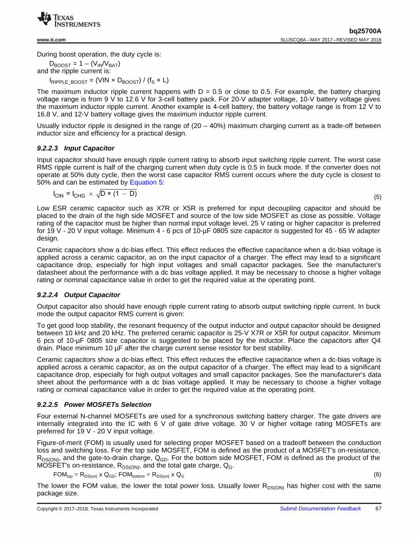
CIN CHGI = I D × (1 D)´ -
67
bq25700Awww.ti.com SLUSCQ8A –MAY 2017–REVISED MAY 2018
Submit Documentation FeedbackCopyright © 2017–2018, Texas Instruments Incorporated
During boost operation, the duty cycle is:DBOOST = 1 – (VIN/VBAT)
and the ripple current is:IRIPPLE_BOOST = (VIN × DBOOST) / (fS × L)
The maximum inductor ripple current happens with D = 0.5 or close to 0.5. For example, the battery chargingvoltage range is from 9 V to 12.6 V for 3-cell battery pack. For 20-V adapter voltage, 10-V battery voltage givesthe maximum inductor ripple current. Another example is 4-cell battery, the battery voltage range is from 12 V to16.8 V, and 12-V battery voltage gives the maximum inductor ripple current.
Usually inductor ripple is designed in the range of (20 – 40%) maximum charging current as a trade-off betweeninductor size and efficiency for a practical design.
9.2.2.3 Input CapacitorInput capacitor should have enough ripple current rating to absorb input switching ripple current. The worst caseRMS ripple current is half of the charging current when duty cycle is 0.5 in buck mode. If the converter does notoperate at 50% duty cycle, then the worst case capacitor RMS current occurs where the duty cycle is closest to50% and can be estimated by Equation 5:
(5)
Low ESR ceramic capacitor such as X7R or X5R is preferred for input decoupling capacitor and should beplaced to the drain of the high side MOSFET and source of the low side MOSFET as close as possible. Voltagerating of the capacitor must be higher than normal input voltage level. 25 V rating or higher capacitor is preferredfor 19 V - 20 V input voltage. Minimum 4 - 6 pcs of 10-µF 0805 size capacitor is suggested for 45 - 65 W adapterdesign.
Ceramic capacitors show a dc-bias effect. This effect reduces the effective capacitance when a dc-bias voltage isapplied across a ceramic capacitor, as on the input capacitor of a charger. The effect may lead to a significantcapacitance drop, especially for high input voltages and small capacitor packages. See the manufacturer'sdatasheet about the performance with a dc bias voltage applied. It may be necessary to choose a higher voltagerating or nominal capacitance value in order to get the required value at the operating point.
9.2.2.4 Output CapacitorOutput capacitor also should have enough ripple current rating to absorb output switching ripple current. In buckmode the output capacitor RMS current is given:
To get good loop stability, the resonant frequency of the output inductor and output capacitor should be designedbetween 10 kHz and 20 kHz. The preferred ceramic capacitor is 25-V X7R or X5R for output capacitor. Minimum6 pcs of 10-µF 0805 size capacitor is suggested to be placed by the inductor. Place the capacitors after Q4drain. Place minimum 10 µF after the charge current sense resistor for best stability.
Ceramic capacitors show a dc-bias effect. This effect reduces the effective capacitance when a dc-bias voltage isapplied across a ceramic capacitor, as on the output capacitor of a charger. The effect may lead to a significantcapacitance drop, especially for high output voltages and small capacitor packages. See the manufacturer's datasheet about the performance with a dc bias voltage applied. It may be necessary to choose a higher voltagerating or nominal capacitance value in order to get the required value at the operating point.
9.2.2.5 Power MOSFETs SelectionFour external N-channel MOSFETs are used for a synchronous switching battery charger. The gate drivers areinternally integrated into the IC with 6 V of gate drive voltage. 30 V or higher voltage rating MOSFETs arepreferred for 19 V - 20 V input voltage.
Figure-of-merit (FOM) is usually used for selecting proper MOSFET based on a tradeoff between the conductionloss and switching loss. For the top side MOSFET, FOM is defined as the product of a MOSFET's on-resistance,RDS(ON), and the gate-to-drain charge, QGD. For the bottom side MOSFET, FOM is defined as the product of theMOSFET's on-resistance, RDS(ON), and the total gate charge, QG.
FOMtop = RDS(on) x QGD; FOMbottom = RDS(on) x QG (6)
The lower the FOM value, the lower the total power loss. Usually lower RDS(ON) has higher cost with the samepackage size.
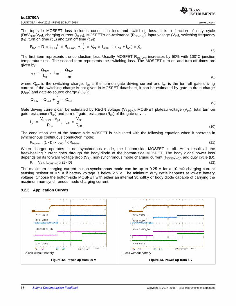
CH1: VBUS
CH2: VDDA
CH3: CHRG_OK
CH4: VSYS
CH1: VBUS
CH2: VDDA
CH3: CHRG_OK
CH4: VSYS
REGN plt plton off
on off
V - V VI = , I =
R R
SW GD GS
1Q = Q + Q
2´
SW SWon off
on off
Q Qt = , t =
I I
2top CHG DS(on) IN CHG on off s
1P = D I R + V I (t + t )
2f´ ´ ´ ´ ´ ´
68
bq25700ASLUSCQ8A –MAY 2017–REVISED MAY 2018 www.ti.com
Submit Documentation Feedback Copyright © 2017–2018, Texas Instruments Incorporated
The top-side MOSFET loss includes conduction loss and switching loss. It is a function of duty cycle(D=VOUT/VIN), charging current (ICHG), MOSFET's on-resistance (RDS(ON)), input voltage (VIN), switching frequency(fS), turn on time (ton) and turn off time (toff):
(7)
The first item represents the conduction loss. Usually MOSFET RDS(ON) increases by 50% with 100°C junctiontemperature rise. The second term represents the switching loss. The MOSFET turn-on and turn-off times aregiven by:
(8)
where Qsw is the switching charge, Ion is the turn-on gate driving current and Ioff is the turn-off gate drivingcurrent. If the switching charge is not given in MOSFET datasheet, it can be estimated by gate-to-drain charge(QGD) and gate-to-source charge (QGS):
(9)
Gate driving current can be estimated by REGN voltage (VREGN), MOSFET plateau voltage (Vplt), total turn-ongate resistance (Ron) and turn-off gate resistance (Roff) of the gate driver:
(10)
The conduction loss of the bottom-side MOSFET is calculated with the following equation when it operates insynchronous continuous conduction mode:
Pbottom = (1 - D) x ICHG2 x RDS(on) (11)
When charger operates in non-synchronous mode, the bottom-side MOSFET is off. As a result all thefreewheeling current goes through the body-diode of the bottom-side MOSFET. The body diode power lossdepends on its forward voltage drop (VF), non-synchronous mode charging current (INONSYNC), and duty cycle (D).
PD = VF x INONSYNC x (1 - D) (12)
The maximum charging current in non-synchronous mode can be up to 0.25 A for a 10-mΩ charging currentsensing resistor or 0.5 A if battery voltage is below 2.5 V. The minimum duty cycle happens at lowest batteryvoltage. Choose the bottom-side MOSFET with either an internal Schottky or body diode capable of carrying themaximum non-synchronous mode charging current.
9.2.3 Application Curves
2-cell without battery
Figure 42. Power Up from 20 V
2-cell without battery
Figure 43. Power Up from 5 V
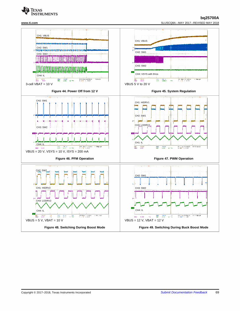
CH1: HIDRV2
CH2: SW2
CH3: LODRV2
CH4: IL
CH2: SW1
CH3: SW2
CH4: IL
CH2: SW1
CH3: SW2
CH4: IL
CH1: HIDRV1
CH2: SW1
CH3: LODRV1
CH1: IL
CH1: VBUS
CH2: SW1
CH3: SW2
CH4: IL
CH1: VBUS
CH2: SW1
CH3: SW2
CH4: VSYS with 9Vos
69
bq25700Awww.ti.com SLUSCQ8A –MAY 2017–REVISED MAY 2018
Submit Documentation FeedbackCopyright © 2017–2018, Texas Instruments Incorporated
3-cell VBAT = 10 V
Figure 44. Power Off from 12 V
VBUS 5 V to 20 V
Figure 45. System Regulation
VBUS = 20 V, VSYS = 10 V, ISYS = 200 mA
Figure 46. PFM Operation Figure 47. PWM Operation
VBUS = 5 V, VBAT = 10 V
Figure 48. Switching During Boost Mode
VBUS = 12 V, VBAT = 12 V
Figure 49. Switching During Buck Boost Mode
CH2:IIN
CH3:ISYS
CH4:IBAT
CH1: EN_OTG
CH2: VBUS
CH1: VSYS
CH2: IIN
CH3: ISYS
CH2: IIN
CH3: ISYS
CH4: IBAT
CH1: VSYS
CH2: IIN
CH3: ISYS
CH1: VSYS
CH2: IIN
CH3: ISYS
70
bq25700ASLUSCQ8A –MAY 2017–REVISED MAY 2018 www.ti.com
Submit Documentation Feedback Copyright © 2017–2018, Texas Instruments Incorporated
VBUS = 12 V/3.3 A, 3-cell, VSYS = 9 V, Without battery
Figure 50. System Regulation in Buck Mode
VBUS = 9 V/3.3 A, 3-cell, VSYS = 9 V, Without battery
Figure 51. System Regulation in Buck Boost Mode
VBUS = 5 V/3.3 A, 3-cell, VSYS = 9 V, Without battery
Figure 52. System Regulation in Boost Mode
VBUS = 20 V/3.3 V, VBAT = 7.5 V
Figure 53. Input Current Regulation in Buck Mode
VBUS = 5 V/3.3 V, VBAT = 7.5 V
Figure 54. Input Current in Boost Mode
VBUS = 5 V
Figure 55. OTG Power Up from 8 V Battery
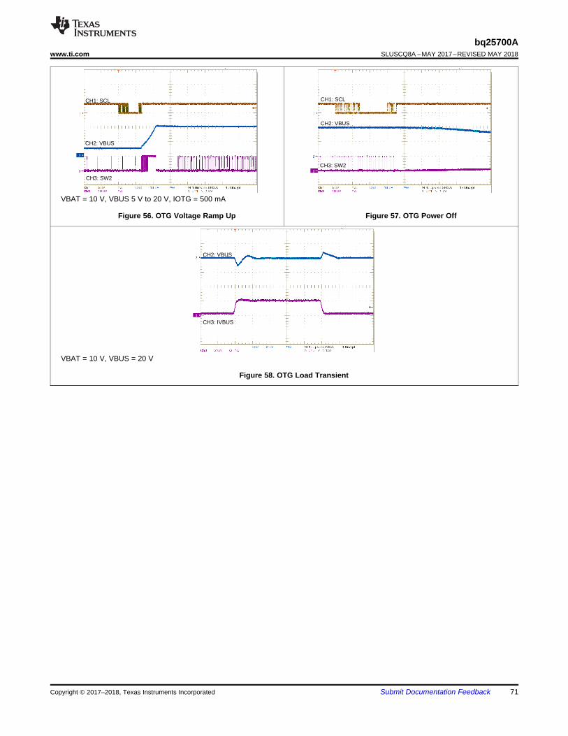
CH2: VBUS
CH3: IVBUS
CH1: SCL
CH2: VBUS
CH3: SW2
CH1: SCL
CH2: VBUS
CH3: SW2
71
bq25700Awww.ti.com SLUSCQ8A –MAY 2017–REVISED MAY 2018
Submit Documentation FeedbackCopyright © 2017–2018, Texas Instruments Incorporated
VBAT = 10 V, VBUS 5 V to 20 V, IOTG = 500 mA
Figure 56. OTG Voltage Ramp Up Figure 57. OTG Power Off
VBAT = 10 V, VBUS = 20 V
Figure 58. OTG Load Transient
72
bq25700ASLUSCQ8A –MAY 2017–REVISED MAY 2018 www.ti.com
Submit Documentation Feedback Copyright © 2017–2018, Texas Instruments Incorporated
10 Power Supply RecommendationsThe valid adapter range is from 3.5 V (VVBUS_CONVEN) to 24 V (ACOV) with at least 500-mA current rating. WhenCHRG_OK goes HIGH, the system is powered from adapter through the charger. When adapter is removed, thesystem is connected to battery through BATFET. Typically the battery depletion threshold should be greater thanthe minimum system voltage so that the battery capacity can be fully utilized for maximum battery life.
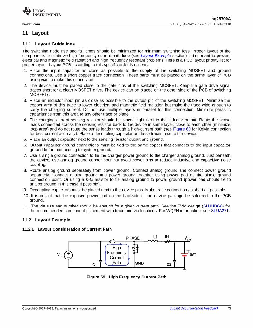
High
Frequency
Current
Path
L1 R1
C2C1 GND
PHASE VBAT
BATVIN
73
bq25700Awww.ti.com SLUSCQ8A –MAY 2017–REVISED MAY 2018
Submit Documentation FeedbackCopyright © 2017–2018, Texas Instruments Incorporated
11 Layout
11.1 Layout GuidelinesThe switching node rise and fall times should be minimized for minimum switching loss. Proper layout of thecomponents to minimize high frequency current path loop (see Layout Example section) is important to preventelectrical and magnetic field radiation and high frequency resonant problems. Here is a PCB layout priority list forproper layout. Layout PCB according to this specific order is essential.1. Place the input capacitor as close as possible to the supply of the switching MOSFET and ground
connections. Use a short copper trace connection. These parts must be placed on the same layer of PCBusing vias to make this connection.
2. The device must be placed close to the gate pins of the switching MOSFET. Keep the gate drive signaltraces short for a clean MOSFET drive. The device can be placed on the other side of the PCB of switchingMOSFETs.
3. Place an inductor input pin as close as possible to the output pin of the switching MOSFET. Minimize thecopper area of this trace to lower electrical and magnetic field radiation but make the trace wide enough tocarry the charging current. Do not use multiple layers in parallel for this connection. Minimize parasiticcapacitance from this area to any other trace or plane.
4. The charging current sensing resistor should be placed right next to the inductor output. Route the senseleads connected across the sensing resistor back to the device in same layer, close to each other (minimizeloop area) and do not route the sense leads through a high-current path (see Figure 60 for Kelvin connectionfor best current accuracy). Place a decoupling capacitor on these traces next to the device.
5. Place an output capacitor next to the sensing resistor output and ground.6. Output capacitor ground connections must be tied to the same copper that connects to the input capacitor
ground before connecting to system ground.7. Use a single ground connection to tie the charger power ground to the charger analog ground. Just beneath
the device, use analog ground copper pour but avoid power pins to reduce inductive and capacitive noisecoupling.
8. Route analog ground separately from power ground. Connect analog ground and connect power groundseparately. Connect analog ground and power ground together using power pad as the single groundconnection point. Or using a 0-Ω resistor to tie analog ground to power ground (power pad should tie toanalog ground in this case if possible).
9. Decoupling capacitors must be placed next to the device pins. Make trace connection as short as possible.10. It is critical that the exposed power pad on the backside of the device package be soldered to the PCB
ground.11. The via size and number should be enough for a given current path. See the EVM design (SLUUBG6) for
the recommended component placement with trace and via locations. For WQFN information, see SLUA271.
11.2 Layout Example
11.2.1 Layout Consideration of Current Path
Figure 59. High Frequency Current Path
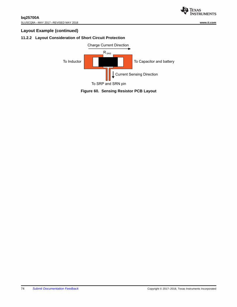
Charge Current Direction
To SRP and SRN pin
R SNS
To Inductor To Capacitor and battery
Current Sensing Direction
74
bq25700ASLUSCQ8A –MAY 2017–REVISED MAY 2018 www.ti.com
Submit Documentation Feedback Copyright © 2017–2018, Texas Instruments Incorporated
Layout Example (continued)11.2.2 Layout Consideration of Short Circuit Protection
Figure 60. Sensing Resistor PCB Layout
75
bq25700Awww.ti.com SLUSCQ8A –MAY 2017–REVISED MAY 2018
Submit Documentation FeedbackCopyright © 2017–2018, Texas Instruments Incorporated
12 Device and Documentation Support
12.1 Device Support
12.1.1 Third-Party Products DisclaimerTI'S PUBLICATION OF INFORMATION REGARDING THIRD-PARTY PRODUCTS OR SERVICES DOES NOTCONSTITUTE AN ENDORSEMENT REGARDING THE SUITABILITY OF SUCH PRODUCTS OR SERVICESOR A WARRANTY, REPRESENTATION OR ENDORSEMENT OF SUCH PRODUCTS OR SERVICES, EITHERALONE OR IN COMBINATION WITH ANY TI PRODUCT OR SERVICE.
12.2 Documentation Support
12.2.1 Related DocumentationFor related documentation see the following:• Semiconductor and IC Package Thermal Metrics Application Report SPRA953• bq2570x Evaluation Module User's Guide SLUUBG6• QFN/SON PCB Attachment Application Report SLUA271
12.3 Receiving Notification of Documentation UpdatesTo receive notification of documentation updates, navigate to the device product folder on ti.com. In the upperright corner, click on Alert me to register and receive a weekly digest of any product information that haschanged. For change details, review the revision history included in any revised document.
12.4 Community ResourcesThe following links connect to TI community resources. Linked contents are provided "AS IS" by the respectivecontributors. They do not constitute TI specifications and do not necessarily reflect TI's views; see TI's Terms ofUse.
TI E2E™ Online Community TI's Engineer-to-Engineer (E2E) Community. Created to foster collaborationamong engineers. At e2e.ti.com, you can ask questions, share knowledge, explore ideas and helpsolve problems with fellow engineers.
Design Support TI's Design Support Quickly find helpful E2E forums along with design support tools andcontact information for technical support.
12.5 TrademarksE2E is a trademark of Texas Instruments.All other trademarks are the property of their respective owners.
12.6 Electrostatic Discharge CautionThese devices have limited built-in ESD protection. The leads should be shorted together or the device placed in conductive foamduring storage or handling to prevent electrostatic damage to the MOS gates.
12.7 GlossarySLYZ022 — TI Glossary.
This glossary lists and explains terms, acronyms, and definitions.
76
bq25700ASLUSCQ8A –MAY 2017–REVISED MAY 2018 www.ti.com
Submit Documentation Feedback Copyright © 2017–2018, Texas Instruments Incorporated
13 Mechanical, Packaging, and Orderable InformationThe following pages include mechanical, packaging, and orderable information. This information is the mostcurrent data available for the designated devices. This data is subject to change without notice and revision ofthis document. For browser-based versions of this data sheet, refer to the left-hand navigation.
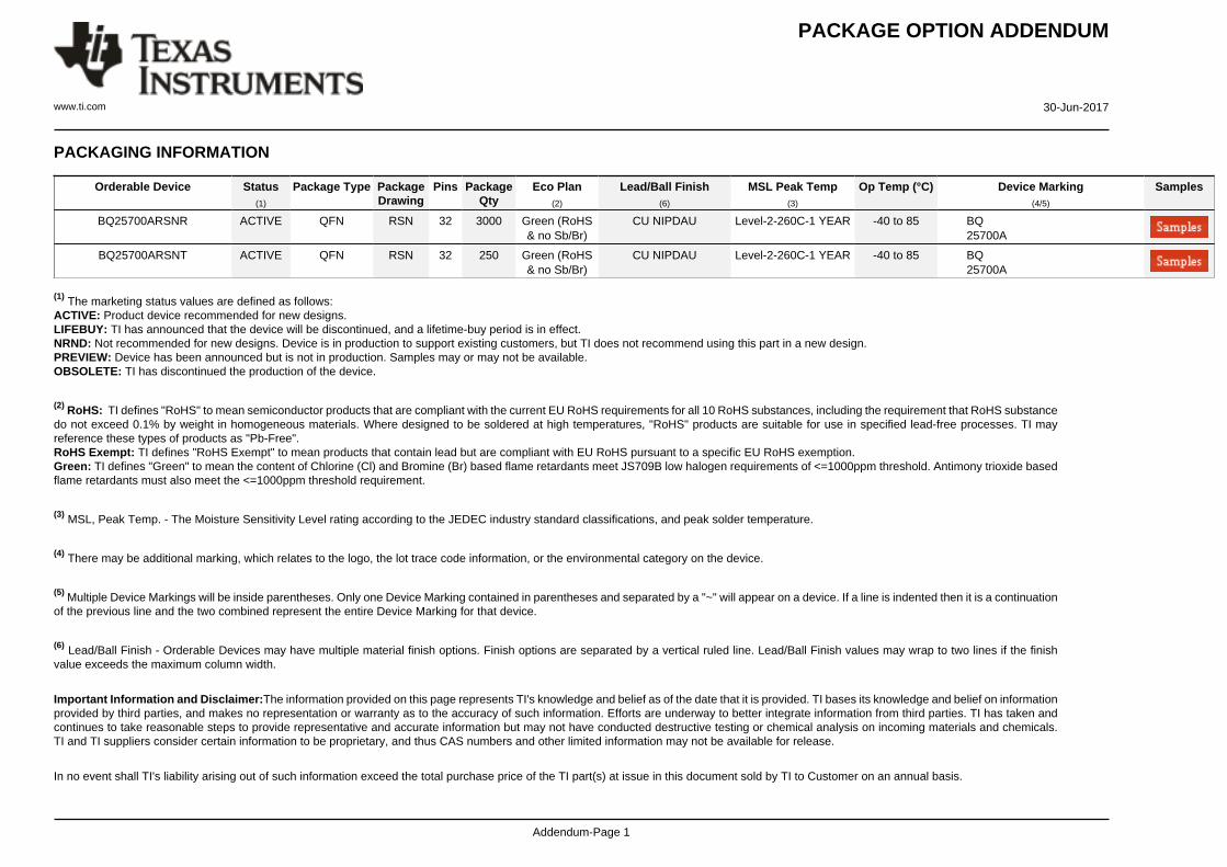
PACKAGE OPTION ADDENDUM
www.ti.com 30-Jun-2017
Addendum-Page 1
PACKAGING INFORMATION
Orderable Device Status(1)
Package Type PackageDrawing
Pins PackageQty
Eco Plan(2)
Lead/Ball Finish(6)
MSL Peak Temp(3)
Op Temp (°C) Device Marking(4/5)
Samples
BQ25700ARSNR ACTIVE QFN RSN 32 3000 Green (RoHS& no Sb/Br)
CU NIPDAU Level-2-260C-1 YEAR -40 to 85 BQ25700A
BQ25700ARSNT ACTIVE QFN RSN 32 250 Green (RoHS& no Sb/Br)
CU NIPDAU Level-2-260C-1 YEAR -40 to 85 BQ25700A
(1) The marketing status values are defined as follows:ACTIVE: Product device recommended for new designs.LIFEBUY: TI has announced that the device will be discontinued, and a lifetime-buy period is in effect.NRND: Not recommended for new designs. Device is in production to support existing customers, but TI does not recommend using this part in a new design.PREVIEW: Device has been announced but is not in production. Samples may or may not be available.OBSOLETE: TI has discontinued the production of the device.
(2) RoHS: TI defines "RoHS" to mean semiconductor products that are compliant with the current EU RoHS requirements for all 10 RoHS substances, including the requirement that RoHS substancedo not exceed 0.1% by weight in homogeneous materials. Where designed to be soldered at high temperatures, "RoHS" products are suitable for use in specified lead-free processes. TI mayreference these types of products as "Pb-Free".RoHS Exempt: TI defines "RoHS Exempt" to mean products that contain lead but are compliant with EU RoHS pursuant to a specific EU RoHS exemption.Green: TI defines "Green" to mean the content of Chlorine (Cl) and Bromine (Br) based flame retardants meet JS709B low halogen requirements of <=1000ppm threshold. Antimony trioxide basedflame retardants must also meet the <=1000ppm threshold requirement.
(3) MSL, Peak Temp. - The Moisture Sensitivity Level rating according to the JEDEC industry standard classifications, and peak solder temperature.
(4) There may be additional marking, which relates to the logo, the lot trace code information, or the environmental category on the device.
(5) Multiple Device Markings will be inside parentheses. Only one Device Marking contained in parentheses and separated by a "~" will appear on a device. If a line is indented then it is a continuationof the previous line and the two combined represent the entire Device Marking for that device.
(6) Lead/Ball Finish - Orderable Devices may have multiple material finish options. Finish options are separated by a vertical ruled line. Lead/Ball Finish values may wrap to two lines if the finishvalue exceeds the maximum column width.
Important Information and Disclaimer:The information provided on this page represents TI's knowledge and belief as of the date that it is provided. TI bases its knowledge and belief on informationprovided by third parties, and makes no representation or warranty as to the accuracy of such information. Efforts are underway to better integrate information from third parties. TI has taken andcontinues to take reasonable steps to provide representative and accurate information but may not have conducted destructive testing or chemical analysis on incoming materials and chemicals.TI and TI suppliers consider certain information to be proprietary, and thus CAS numbers and other limited information may not be available for release.
In no event shall TI's liability arising out of such information exceed the total purchase price of the TI part(s) at issue in this document sold by TI to Customer on an annual basis.
PACKAGE OPTION ADDENDUM
www.ti.com 30-Jun-2017
Addendum-Page 2
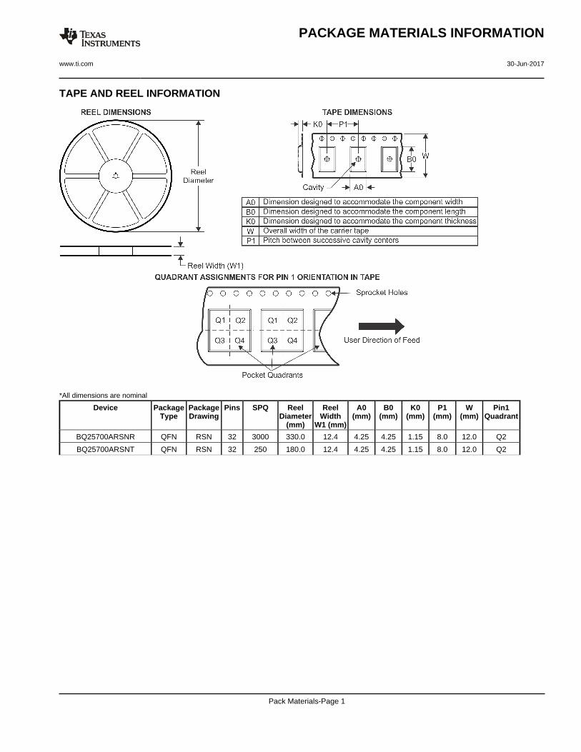
TAPE AND REEL INFORMATION
*All dimensions are nominal
Device PackageType
PackageDrawing
Pins SPQ ReelDiameter
(mm)
ReelWidth
W1 (mm)
A0(mm)
B0(mm)
K0(mm)
P1(mm)
W(mm)
Pin1Quadrant
BQ25700ARSNR QFN RSN 32 3000 330.0 12.4 4.25 4.25 1.15 8.0 12.0 Q2
BQ25700ARSNT QFN RSN 32 250 180.0 12.4 4.25 4.25 1.15 8.0 12.0 Q2
PACKAGE MATERIALS INFORMATION
www.ti.com 30-Jun-2017
Pack Materials-Page 1
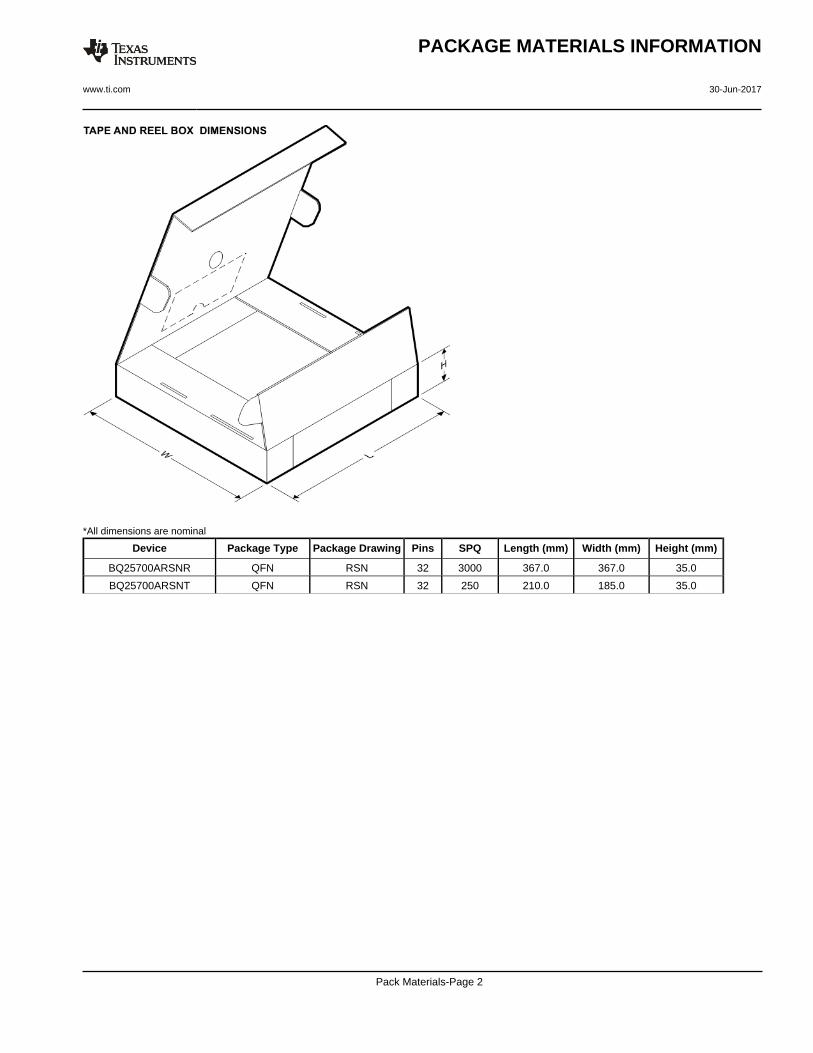
*All dimensions are nominal
Device Package Type Package Drawing Pins SPQ Length (mm) Width (mm) Height (mm)
BQ25700ARSNR QFN RSN 32 3000 367.0 367.0 35.0
BQ25700ARSNT QFN RSN 32 250 210.0 185.0 35.0
PACKAGE MATERIALS INFORMATION
www.ti.com 30-Jun-2017
Pack Materials-Page 2
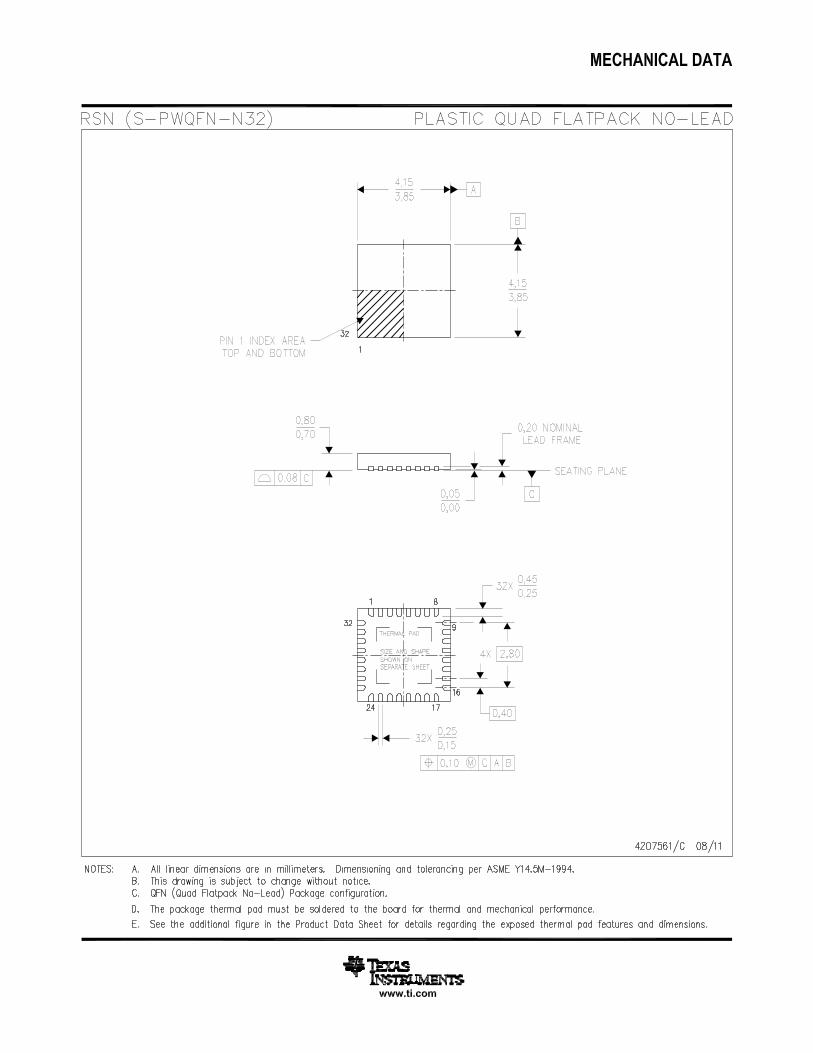
IMPORTANT NOTICE
Texas Instruments Incorporated (TI) reserves the right to make corrections, enhancements, improvements and other changes to itssemiconductor products and services per JESD46, latest issue, and to discontinue any product or service per JESD48, latest issue. Buyersshould obtain the latest relevant information before placing orders and should verify that such information is current and complete.TI’s published terms of sale for semiconductor products (http://www.ti.com/sc/docs/stdterms.htm) apply to the sale of packaged integratedcircuit products that TI has qualified and released to market. Additional terms may apply to the use or sale of other types of TI products andservices.Reproduction of significant portions of TI information in TI data sheets is permissible only if reproduction is without alteration and isaccompanied by all associated warranties, conditions, limitations, and notices. TI is not responsible or liable for such reproduceddocumentation. Information of third parties may be subject to additional restrictions. Resale of TI products or services with statementsdifferent from or beyond the parameters stated by TI for that product or service voids all express and any implied warranties for theassociated TI product or service and is an unfair and deceptive business practice. TI is not responsible or liable for any such statements.Buyers and others who are developing systems that incorporate TI products (collectively, “Designers”) understand and agree that Designersremain responsible for using their independent analysis, evaluation and judgment in designing their applications and that Designers havefull and exclusive responsibility to assure the safety of Designers' applications and compliance of their applications (and of all TI productsused in or for Designers’ applications) with all applicable regulations, laws and other applicable requirements. Designer represents that, withrespect to their applications, Designer has all the necessary expertise to create and implement safeguards that (1) anticipate dangerousconsequences of failures, (2) monitor failures and their consequences, and (3) lessen the likelihood of failures that might cause harm andtake appropriate actions. Designer agrees that prior to using or distributing any applications that include TI products, Designer willthoroughly test such applications and the functionality of such TI products as used in such applications.TI’s provision of technical, application or other design advice, quality characterization, reliability data or other services or information,including, but not limited to, reference designs and materials relating to evaluation modules, (collectively, “TI Resources”) are intended toassist designers who are developing applications that incorporate TI products; by downloading, accessing or using TI Resources in anyway, Designer (individually or, if Designer is acting on behalf of a company, Designer’s company) agrees to use any particular TI Resourcesolely for this purpose and subject to the terms of this Notice.TI’s provision of TI Resources does not expand or otherwise alter TI’s applicable published warranties or warranty disclaimers for TIproducts, and no additional obligations or liabilities arise from TI providing such TI Resources. TI reserves the right to make corrections,enhancements, improvements and other changes to its TI Resources. TI has not conducted any testing other than that specificallydescribed in the published documentation for a particular TI Resource.Designer is authorized to use, copy and modify any individual TI Resource only in connection with the development of applications thatinclude the TI product(s) identified in such TI Resource. NO OTHER LICENSE, EXPRESS OR IMPLIED, BY ESTOPPEL OR OTHERWISETO ANY OTHER TI INTELLECTUAL PROPERTY RIGHT, AND NO LICENSE TO ANY TECHNOLOGY OR INTELLECTUAL PROPERTYRIGHT OF TI OR ANY THIRD PARTY IS GRANTED HEREIN, including but not limited to any patent right, copyright, mask work right, orother intellectual property right relating to any combination, machine, or process in which TI products or services are used. Informationregarding or referencing third-party products or services does not constitute a license to use such products or services, or a warranty orendorsement thereof. Use of TI Resources may require a license from a third party under the patents or other intellectual property of thethird party, or a license from TI under the patents or other intellectual property of TI.TI RESOURCES ARE PROVIDED “AS IS” AND WITH ALL FAULTS. TI DISCLAIMS ALL OTHER WARRANTIES ORREPRESENTATIONS, EXPRESS OR IMPLIED, REGARDING RESOURCES OR USE THEREOF, INCLUDING BUT NOT LIMITED TOACCURACY OR COMPLETENESS, TITLE, ANY EPIDEMIC FAILURE WARRANTY AND ANY IMPLIED WARRANTIES OFMERCHANTABILITY, FITNESS FOR A PARTICULAR PURPOSE, AND NON-INFRINGEMENT OF ANY THIRD PARTY INTELLECTUALPROPERTY RIGHTS. TI SHALL NOT BE LIABLE FOR AND SHALL NOT DEFEND OR INDEMNIFY DESIGNER AGAINST ANY CLAIM,INCLUDING BUT NOT LIMITED TO ANY INFRINGEMENT CLAIM THAT RELATES TO OR IS BASED ON ANY COMBINATION OFPRODUCTS EVEN IF DESCRIBED IN TI RESOURCES OR OTHERWISE. IN NO EVENT SHALL TI BE LIABLE FOR ANY ACTUAL,DIRECT, SPECIAL, COLLATERAL, INDIRECT, PUNITIVE, INCIDENTAL, CONSEQUENTIAL OR EXEMPLARY DAMAGES INCONNECTION WITH OR ARISING OUT OF TI RESOURCES OR USE THEREOF, AND REGARDLESS OF WHETHER TI HAS BEENADVISED OF THE POSSIBILITY OF SUCH DAMAGES.Unless TI has explicitly designated an individual product as meeting the requirements of a particular industry standard (e.g., ISO/TS 16949and ISO 26262), TI is not responsible for any failure to meet such industry standard requirements.Where TI specifically promotes products as facilitating functional safety or as compliant with industry functional safety standards, suchproducts are intended to help enable customers to design and create their own applications that meet applicable functional safety standardsand requirements. Using products in an application does not by itself establish any safety features in the application. Designers mustensure compliance with safety-related requirements and standards applicable to their applications. Designer may not use any TI products inlife-critical medical equipment unless authorized officers of the parties have executed a special contract specifically governing such use.Life-critical medical equipment is medical equipment where failure of such equipment would cause serious bodily injury or death (e.g., lifesupport, pacemakers, defibrillators, heart pumps, neurostimulators, and implantables). Such equipment includes, without limitation, allmedical devices identified by the U.S. Food and Drug Administration as Class III devices and equivalent classifications outside the U.S.TI may expressly designate certain products as completing a particular qualification (e.g., Q100, Military Grade, or Enhanced Product).Designers agree that it has the necessary expertise to select the product with the appropriate qualification designation for their applicationsand that proper product selection is at Designers’ own risk. Designers are solely responsible for compliance with all legal and regulatoryrequirements in connection with such selection.Designer will fully indemnify TI and its representatives against any damages, costs, losses, and/or liabilities arising out of Designer’s non-compliance with the terms and provisions of this Notice.
Mailing Address: Texas Instruments, Post Office Box 655303, Dallas, Texas 75265Copyright © 2018, Texas Instruments Incorporated