
Le Quartz, 75 Cours Emile Zola –
69100 Villeurbanne, France
Tel : +33 472 83 01 80 - Fax : +33 472 83 01 83
Web: http://www.yole.fr
Semi Networking Day
Packaging – Key for System Integration
© 2013• 22013 Copyrights © Yole Développement SA. All right reserved.
Christophe Fitamant
Sales & Marketing Director, Yole Développement
Christophe Fitamant joined Yole Développement in 2013 to lead Média and Sales activities. He holds
an engineering degree of INP Grenoble - Phelma - with a major in Chemical Process Engineering. He
has worked at IBM Corbeil-Essonnes, and Applied Materials. He’s lived in California when he managed
the Applied etch product support group for Taiwan and Japan. Back to France for Lam Research he
first took the responsibility of the ST Crolles site, before taking the Sales Account Management for
Europe. With the acquisition of SEZ in Austria by Lam in 2008, he led Sales and Marketing for Lam
penetration in MEMS and Advanced Packaging for Clean.
Semi Networking Day
© 2013• 3
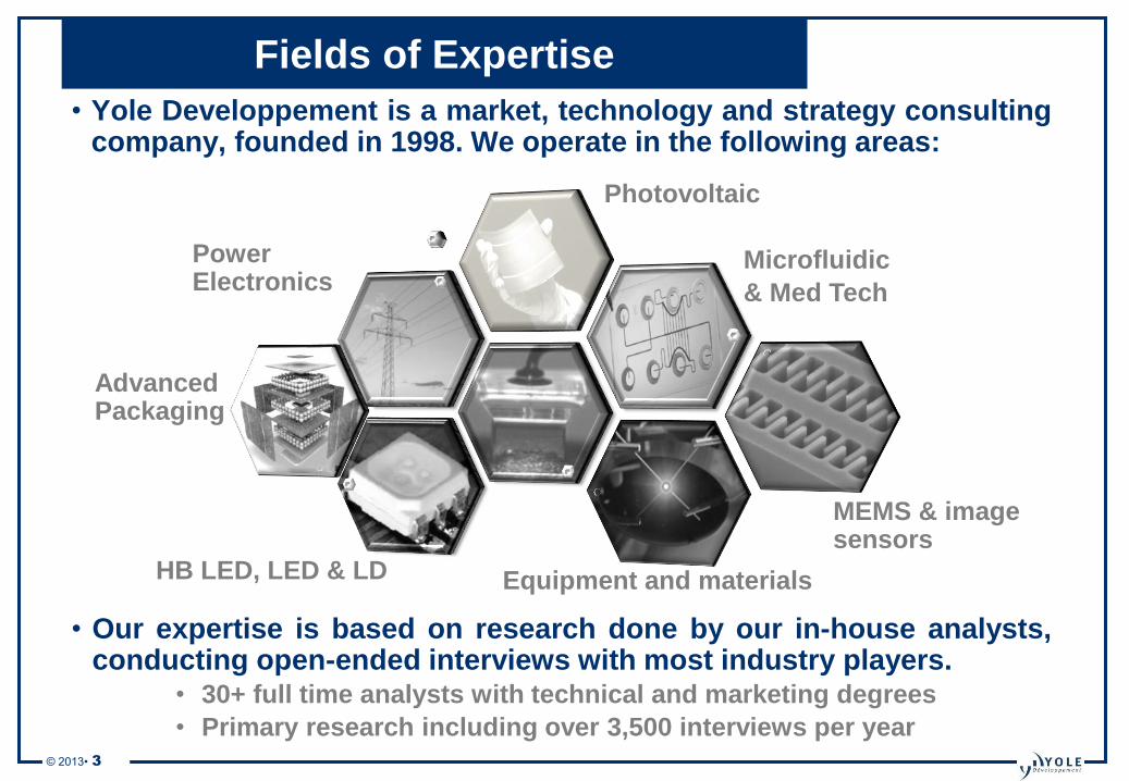
Fields of Expertise
• Yole Developpement is a market, technology and strategy consultingcompany, founded in 1998. We operate in the following areas:
• Our expertise is based on research done by our in-house analysts,conducting open-ended interviews with most industry players.
• 30+ full time analysts with technical and marketing degrees
• Primary research including over 3,500 interviews per year
MEMS & image sensors
Photovoltaic
Advanced Packaging
Microfluidic
& Med Tech
Power Electronics
HB LED, LED & LD Equipment and materials

© 2013• 42013 Copyrights © Yole Développement SA. All right reserved.
Yole Activities in a Nutshell
MEDIANews feed / Magazines / Webcasts
REPORTSMarket & technology
Patent Analysis
Reverse costing report
CONSULTINGMarket research
Technology & Strategy
Patent Analysis
www.yole.fr
YOLE FINANCE M&A / Due Diligence /
Fund raising services
© 2013• 52013 Copyrights © Yole Développement SA. All right reserved.
Rozalia Beica
Chief Technical Officer, Yole Développement
Rozalia Beica is the CTO and Business Unit Manager leading Advanced / 3D Packaging and
Semiconductor Manufacturing activities within Yole Développement. For more than 15 years she has
been involved in research, strategic marketing and application of WLP and 3D/TSV at materials (Rohm
and Haas), equipment (Semitool, Applied Materials, Lam Research) and device manufacturing (Maxim
IC) organizations.
Rozalia has authored over 50 papers and publications and she is actively participating in several 3D &
Advanced Packaging Committees worldwide.
Rozalia holds a M.Sc. in Chemical Engineering (Romania), a M. Sc. In Management of Technology
(USA) and a GXMBA from IE University (Spain).
Semi Networking Day
© 2013
Copyrights © Yole Développement SA. All rights reserved.
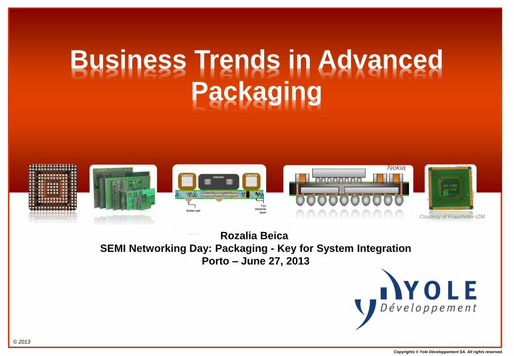
Business Trends in Advanced
Packaging
Courtesy of Fraunhofer-IZM
Rozalia Beica
SEMI Networking Day: Packaging - Key for System Integration
Porto – June 27, 2013
Nokia
© 2013 • 7Copyrights © Yole Développement SA. All rights reserved.
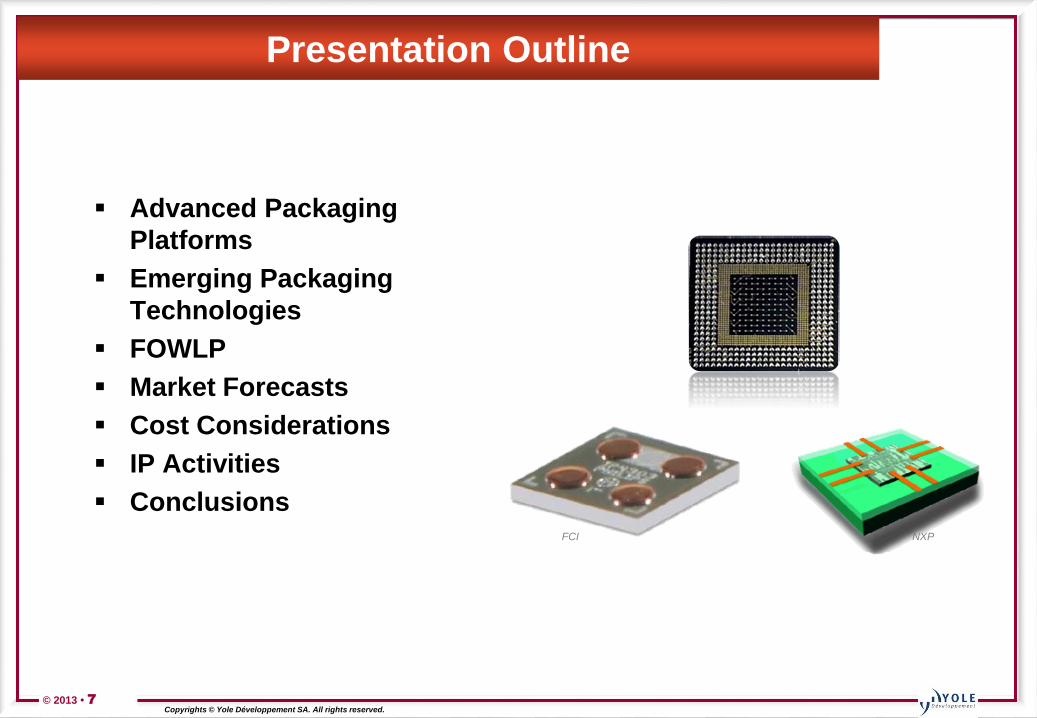
Presentation Outline
FCI NXP
Advanced Packaging
Platforms
Emerging Packaging
Technologies
FOWLP
Market Forecasts
Cost Considerations
IP Activities
Conclusions
© 2013 • 8Copyrights © Yole Développement SA. All rights reserved.
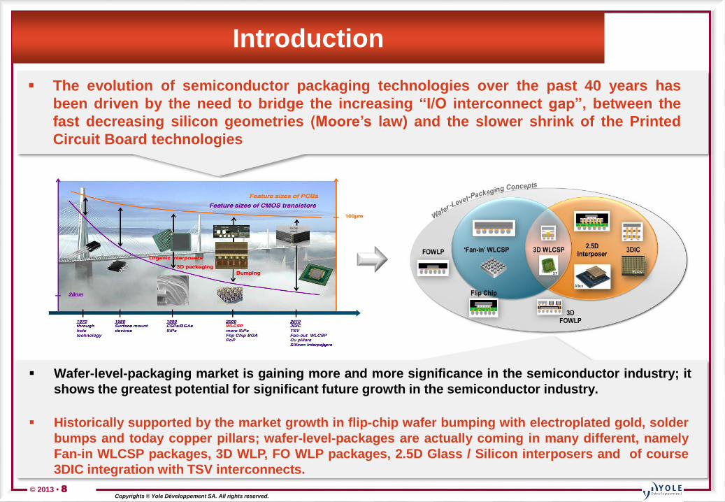
Introduction
Wafer-level-packaging market is gaining more and more significance in the semiconductor industry; it
shows the greatest potential for significant future growth in the semiconductor industry.
Historically supported by the market growth in flip-chip wafer bumping with electroplated gold, solder
bumps and today copper pillars; wafer-level-packages are actually coming in many different, namely
Fan-in WLCSP packages, 3D WLP, FO WLP packages, 2.5D Glass / Silicon interposers and of course
3DIC integration with TSV interconnects.
The evolution of semiconductor packaging technologies over the past 40 years has
been driven by the need to bridge the increasing “I/O interconnect gap”, between the
fast decreasing silicon geometries (Moore’s law) and the slower shrink of the Printed
Circuit Board technologies
© 2013 • 9Copyrights © Yole Développement SA. All rights reserved.
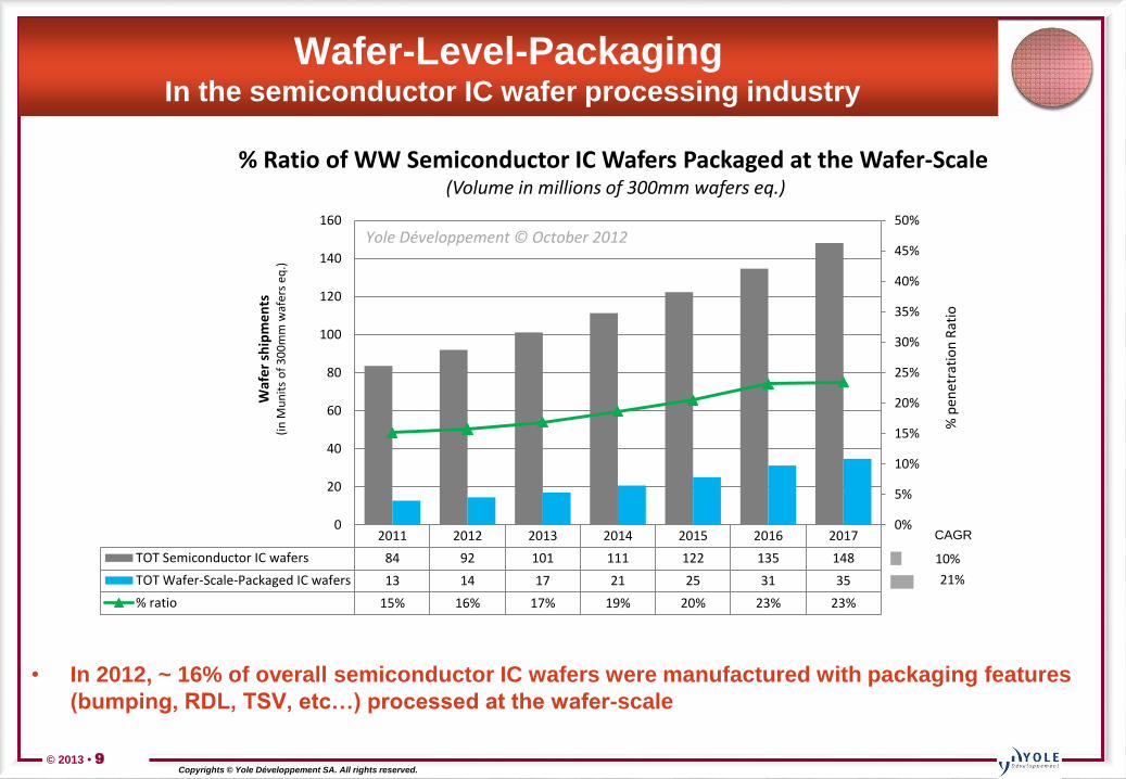
2011 2012 2013 2014 2015 2016 2017
TOT Semiconductor IC wafers 84 92 101 111 122 135 148
TOT Wafer-Scale-Packaged IC wafers 13 14 17 21 25 31 35
% ratio 15% 16% 17% 19% 20% 23% 23%
0%
5%
10%
15%
20%
25%
30%
35%
40%
45%
50%
0
20
40
60
80
100
120
140
160
% p
enet
rati
on
Rat
io
Waf
er
ship
me
nts
(i
n M
un
its
of
30
0m
m w
afer
s eq
.)
% Ratio of WW Semiconductor IC Wafers Packaged at the Wafer-Scale(Volume in millions of 300mm wafers eq.)
Yole Développement © October 2012
Wafer-Level-PackagingIn the semiconductor IC wafer processing industry
• In 2012, ~ 16% of overall semiconductor IC wafers were manufactured with packaging features
(bumping, RDL, TSV, etc…) processed at the wafer-scale
CAGR
21%
10%
© 2013 • 10Copyrights © Yole Développement SA. All rights reserved.
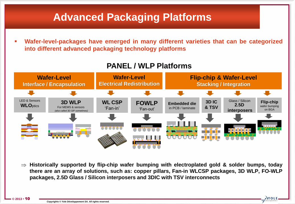
Advanced Packaging Platforms
PANEL / WLP Platforms
Wafer-Level Electrical Redistribution
Flip-chip & Wafer-LevelStacking / Integration
WL CSP‘Fan-in’
FOWLP‘Fan-out’
Glass / Silicon Flip-chip wafer bumping
on BGA
3D IC
& TSVEmbedded die in PCB / laminate
Wafer-Level Interface / Encapsulation
3D WLPFor MEMS & sensors
(also called 3D SiP sometimes)
LED & Sensors
WLOptics 2.5D
interposers
Historically supported by flip-chip wafer bumping with electroplated gold & solder bumps, today
there are an array of solutions, such as: copper pillars, Fan-in WLCSP packages, 3D WLP, FO-WLP
packages, 2.5D Glass / Silicon interposers and 3DIC with TSV interconnects
Wafer-level-packages have emerged in many different varieties that can be categorized
into different advanced packaging technology platforms
© 2013 • 11Copyrights © Yole Développement SA. All rights reserved.
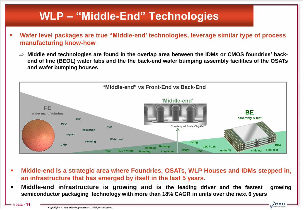
WLP – “Middle-End” Technologies
FEwafer manufacturing
‘Middle-end’
BEassembly & testetch
implant
CVD
PVD
CMP
Wafer test
TSV bumpingRDL / wiring C2W
C2C / C2S
underfill molding Final testhandling
thinning BGAdicing
inspection
cleaning
“Middle-end” vs Front-End vs Back-End
inspection W2W
Courtesy of Stats ChipPAC
Wafer level packages are true “Middle-end’ technologies, leverage similar type of process
manufacturing know-how
Middle-end is a strategic area where Foundries, OSATs, WLP Houses and IDMs stepped in,
an infrastructure that has emerged by itself in the last 5 years.
Middle-end infrastructure is growing and is the leading driver and the fastest growing
semiconductor packaging technology with more than 18% CAGR in units over the next 6 years
Middle end technologies are found in the overlap area between the IDMs or CMOS foundries’ back-
end of line (BEOL) wafer fabs and the the back-end wafer bumping assembly facilities of the OSATs
and wafer bumping houses
© 2013 • 12Copyrights © Yole Développement SA. All rights reserved.
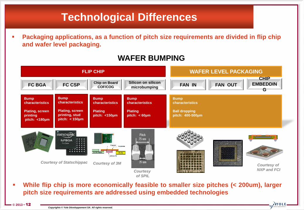
Technological Differences
Bump
characteristics
Plating
pitch: < 60µm
WAFER BUMPING
FLIP CHIP WAFER LEVEL PACKAGING
FC BGA FC CSP FAN IN FAN OUT
Bump
characteristics
Plating, screen
printing
pitch: <180µm
Bump
characteristics
Plating, screen
printing, stud
pitch: < 150µm
Courtesy of Statschippac
CHIP
EMBEDDIN
G
Chip on Board
COF/COG
Bump
characteristics
Ball dropping
pitch: 400-500µm
Bump
characteristics
Plating
pitch: <150µm
Courtesy of
NXP and FCI
Courtesy of 3M
Silicon on silicon
microbumping
Courtesy
of SPIL
Packaging applications, as a function of pitch size requirements are divided in flip chip
and wafer level packaging.
While flip chip is more economically feasible to smaller size pitches (< 200um), larger
pitch size requirements are addressed using embedded technologies
© 2013 • 13Copyrights © Yole Développement SA. All rights reserved.
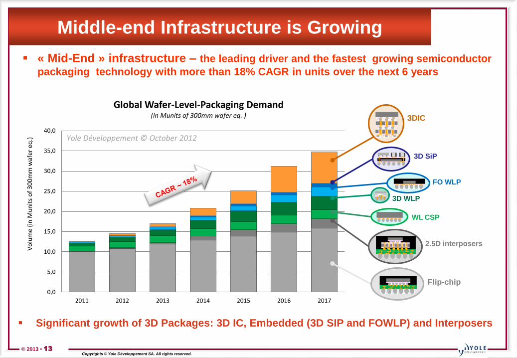
Middle-end Infrastructure is Growing
Significant growth of 3D Packages: 3D IC, Embedded (3D SIP and FOWLP) and Interposers
0,0
5,0
10,0
15,0
20,0
25,0
30,0
35,0
40,0
2011 2012 2013 2014 2015 2016 2017
Vo
lum
e (i
n M
un
its
of
30
0m
m w
afer
eq
.)
Global Wafer-Level-Packaging Demand(in Munits of 300mm wafer eq. )
Yole Développement © October 2012
3DIC
Flip-chip
2.5D interposers
3D WLP
WL CSP
FO WLP
3D SiP
« Mid-End » infrastructure – the leading driver and the fastest growing semiconductor
packaging technology with more than 18% CAGR in units over the next 6 years
© 2013 • 14Copyrights © Yole Développement SA. All rights reserved.
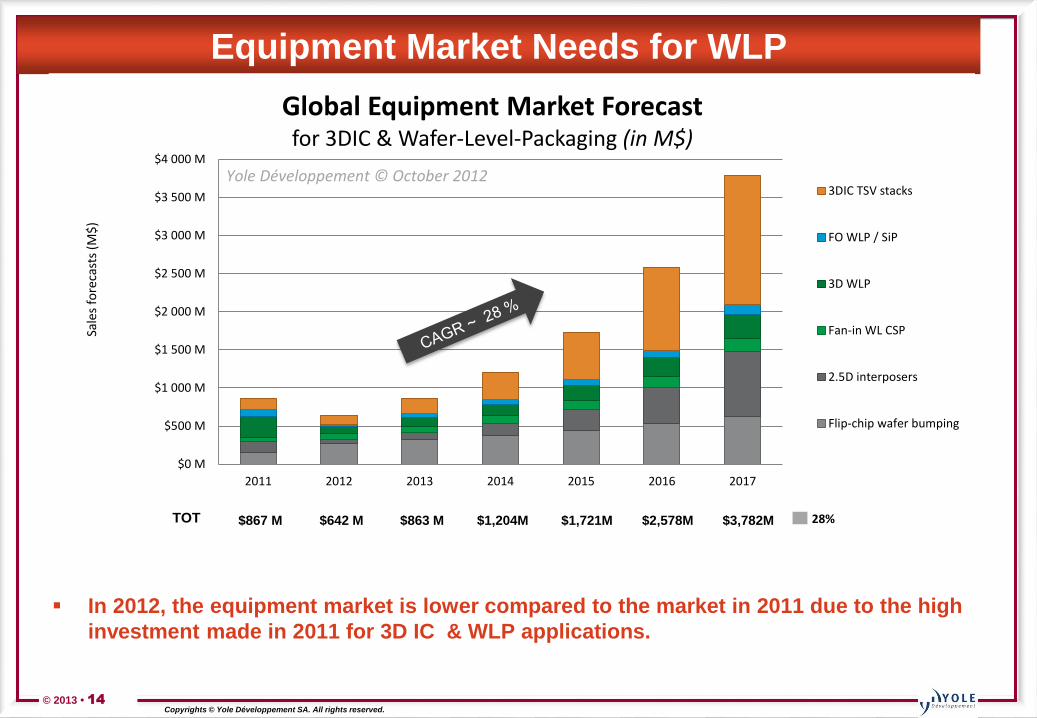
In 2012, the equipment market is lower compared to the market in 2011 due to the high
investment made in 2011 for 3D IC & WLP applications.
TOT $867 M $642 M $863 M $1,204M $1,721M $2,578M $3,782M
Equipment Market Needs for WLP
28%
$0 M
$500 M
$1 000 M
$1 500 M
$2 000 M
$2 500 M
$3 000 M
$3 500 M
$4 000 M
2011 2012 2013 2014 2015 2016 2017
Sale
s fo
reca
sts
(M$
)
Global Equipment Market Forecastfor 3DIC & Wafer-Level-Packaging (in M$)
3DIC TSV stacks
FO WLP / SiP
3D WLP
Fan-in WL CSP
2.5D interposers
Flip-chip wafer bumping
Yole Développement © October 2012
© 2013 • 15Copyrights © Yole Développement SA. All rights reserved.
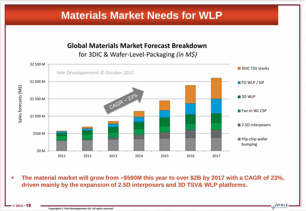
2011 2012 2013 2014 2015 2016 2017
Global Materials market forecast breakdownfor 3DIC & Wafer-Level-Packaging (in M$)
The material market will grow from ~$590M this year to over $2B by 2017 with a CAGR of 23%,
driven mainly by the expansion of 2.5D interposers and 3D TSV& WLP platforms.
CAGR
$0 M
$500 M
$1 000 M
$1 500 M
$2 000 M
$2 500 M
2011 2012 2013 2014 2015 2016 2017
Sale
s fo
reca
sts
(M$
)
Global Materials Market Forecast Breakdownfor 3DIC & Wafer-Level-Packaging (in M$)
3DIC TSV stacks
FO WLP / SiP
3D WLP
Fan-in WL CSP
2.5D interposers
Flip-chip waferbumping
Yole Développement © October 2012
Materials Market Needs for WLP
© 2013 • 16Copyrights © Yole Développement SA. All rights reserved.
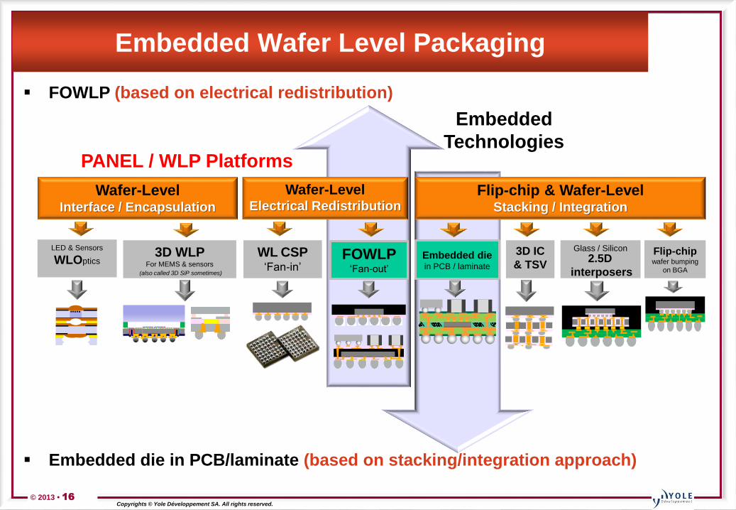
FOWLP (based on electrical redistribution)
Embedded die in PCB/laminate (based on stacking/integration approach)
Embedded Wafer Level Packaging
PANEL / WLP Platforms
Wafer-Level Electrical Redistribution
Flip-chip & Wafer-LevelStacking / Integration
WL CSP‘Fan-in’
FOWLP‘Fan-out’
Glass / Silicon Flip-chip wafer bumping
on BGA
3D IC
& TSVEmbedded die in PCB / laminate
Wafer-Level Interface / Encapsulation
3D WLPFor MEMS & sensors
(also called 3D SiP sometimes)
LED & Sensors
WLOptics 2.5D
interposers
Embedded
Technologies
© 2013 • 17Copyrights © Yole Développement SA. All rights reserved.
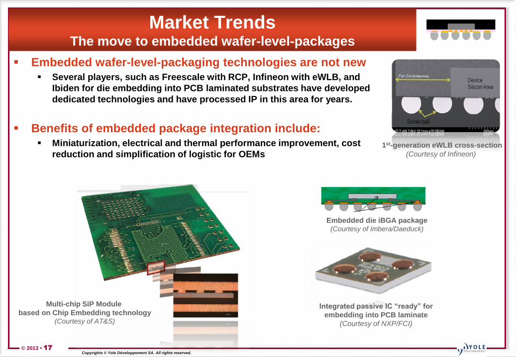
Market Trends The move to embedded wafer-level-packages
Embedded wafer-level-packaging technologies are not new Several players, such as Freescale with RCP, Infineon with eWLB, and
Ibiden for die embedding into PCB laminated substrates have developed
dedicated technologies and have processed IP in this area for years.
Benefits of embedded package integration include: Miniaturization, electrical and thermal performance improvement, cost
reduction and simplification of logistic for OEMs1st-generation eWLB cross-section
(Courtesy of Infineon)
Integrated passive IC “ready” for
embedding into PCB laminate
(Courtesy of NXP/FCI)
Embedded die iBGA package(Courtesy of Imbera/Daeduck)
Multi-chip SiP Module
based on Chip Embedding technology(Courtesy of AT&S)
© 2013 • 18Copyrights © Yole Développement SA. All rights reserved.
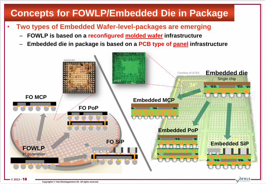
Concepts for FOWLP/Embedded Die in Package
• Two types of Embedded Wafer-level-packages are emerging
– FOWLP is based on a reconfigured molded wafer infrastructure
– Embedded die in package is based on a PCB type of panel infrastructure
FOWLP1st generation
Embedded dieSingle chip
Embedded SiP
Embedded PoP
FO MCP
FO SiP
FO PoP
Embedded MCP
Courtesy of AT&S
AT&S
NANIUM
© 2013
Copyrights © Yole Développement SA. All rights reserved.
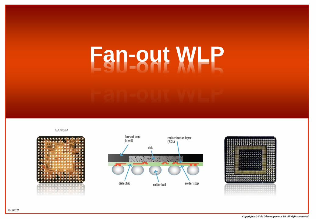
Fan-out WLP
NANIUM
© 2013 • 20Copyrights © Yole Développement SA. All rights reserved.
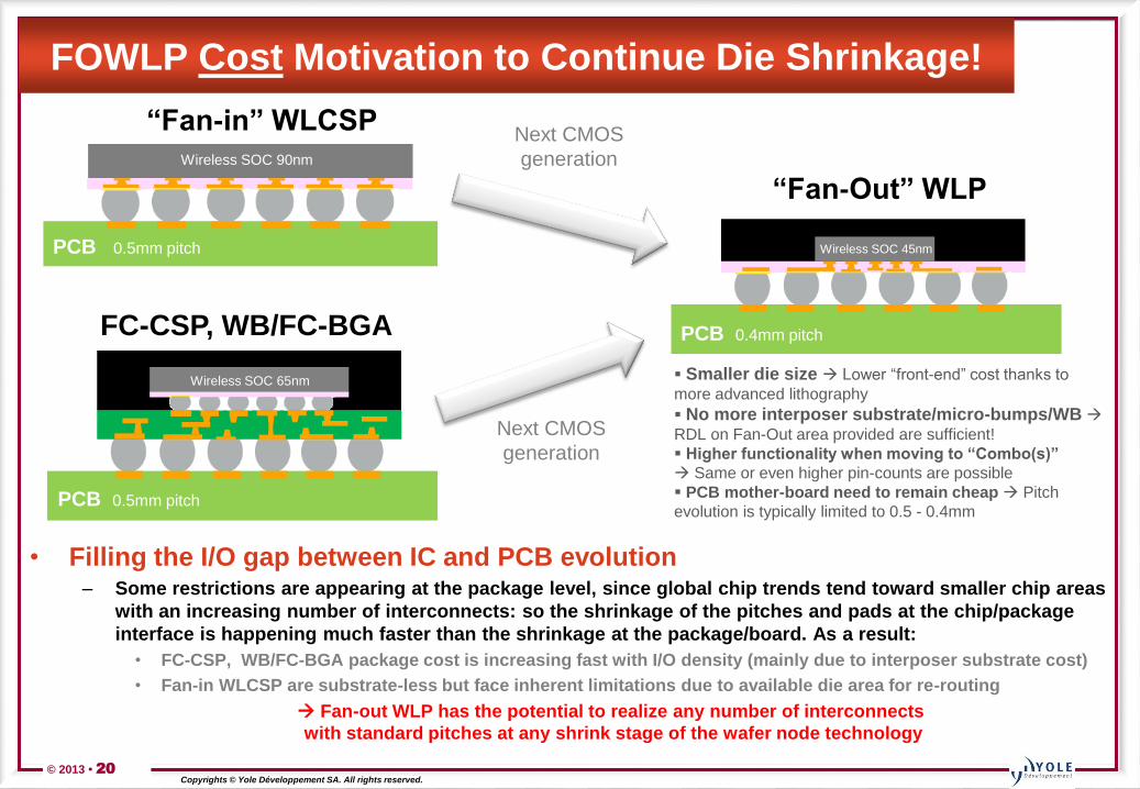
FOWLP Cost Motivation to Continue Die Shrinkage!
• Filling the I/O gap between IC and PCB evolution– Some restrictions are appearing at the package level, since global chip trends tend toward smaller chip areas
with an increasing number of interconnects: so the shrinkage of the pitches and pads at the chip/package
interface is happening much faster than the shrinkage at the package/board. As a result:
• FC-CSP, WB/FC-BGA package cost is increasing fast with I/O density (mainly due to interposer substrate cost)
• Fan-in WLCSP are substrate-less but face inherent limitations due to available die area for re-routing
Fan-out WLP has the potential to realize any number of interconnects
with standard pitches at any shrink stage of the wafer node technology
PCB 0.5mm pitch
Wireless SOC 90nm
“Fan-in” WLCSP
PCB 0.4mm pitch
Wireless SOC 45nm
“Fan-Out” WLP
Next CMOS
generation
Smaller die size Lower “front-end” cost thanks to
more advanced lithography
No more interposer substrate/micro-bumps/WB RDL on Fan-Out area provided are sufficient!
Higher functionality when moving to “Combo(s)”
Same or even higher pin-counts are possible
PCB mother-board need to remain cheap Pitch
evolution is typically limited to 0.5 - 0.4mm
Next CMOS
generation
PCB 0.5mm pitch
Wireless SOC 65nm
FC-CSP, WB/FC-BGA
© 2013 • 21Copyrights © Yole Développement SA. All rights reserved.
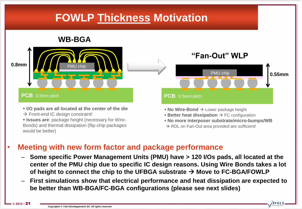
FOWLP Thickness Motivation
• Meeting with new form factor and package performance
– Some specific Power Management Units (PMU) have > 120 I/Os pads, all located at the
center of the PMU chip due to specific IC design reasons. Using Wire Bonds takes a lot
of height to connect the chip to the UFBGA substrate Move to FC-BGA/FOWLP
– First simulations show that electrical performance and heat dissipation are expected to
be better than WB-BGA/FC-BGA configurations (please see next slides)
PCB 0.5mm pitch
PMU chip
“Fan-Out” WLP
No Wire-Bond Lower package height
Better heat dissipation FC configuration
No more interposer substrate/micro-bumps/WB
RDL on Fan-Out area provided are sufficient!
0.55mm
PCB 0.5mm pitch
PMU chip
WB-BGA
I/O pads are all located at the center of the die
Front-end IC design constraint!
Issues are: package height (necessary for Wire-
Bonds) and thermal dissipation (flip-chip packages
would be better)
0.8mm
© 2013 • 22Copyrights © Yole Développement SA. All rights reserved.
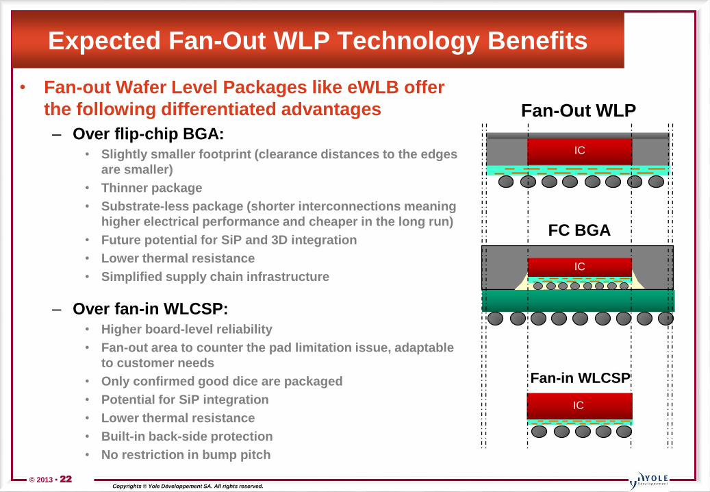
Expected Fan-Out WLP Technology Benefits
• Fan-out Wafer Level Packages like eWLB offer
the following differentiated advantages
– Over flip-chip BGA:• Slightly smaller footprint (clearance distances to the edges
are smaller)
• Thinner package
• Substrate-less package (shorter interconnections meaning
higher electrical performance and cheaper in the long run)
• Future potential for SiP and 3D integration
• Lower thermal resistance
• Simplified supply chain infrastructure
– Over fan-in WLCSP:• Higher board-level reliability
• Fan-out area to counter the pad limitation issue, adaptable
to customer needs
• Only confirmed good dice are packaged
• Potential for SiP integration
• Lower thermal resistance
• Built-in back-side protection
• No restriction in bump pitch
Fan-Out WLP
FC BGA
Fan-in WLCSP
IC
IC
IC
© 2013 • 23Copyrights © Yole Développement SA. All rights reserved.
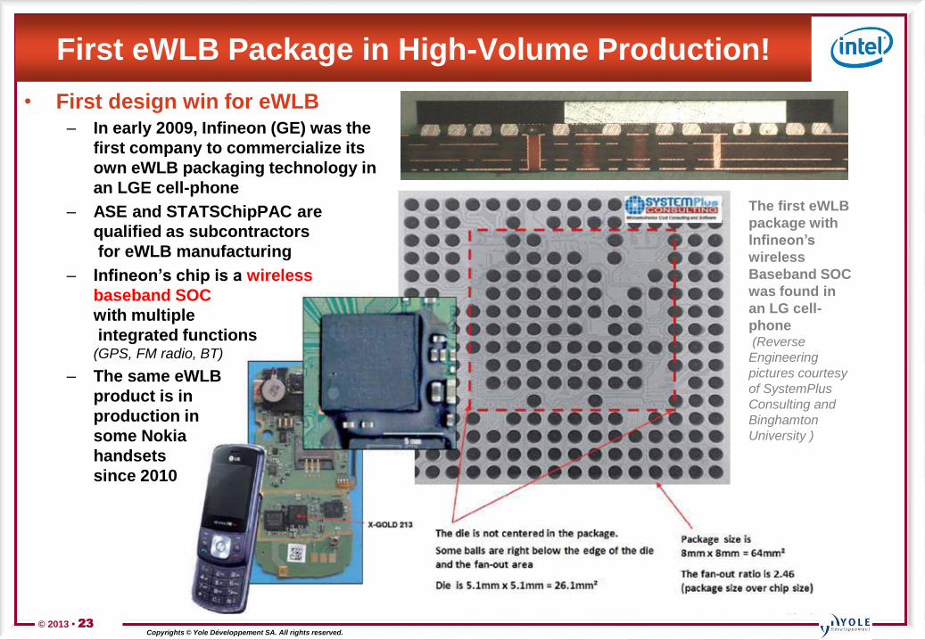
First eWLB Package in High-Volume Production!
• First design win for eWLB– In early 2009, Infineon (GE) was the
first company to commercialize its
own eWLB packaging technology in
an LGE cell-phone
– ASE and STATSChipPAC are
qualified as subcontractors
for eWLB manufacturing
– Infineon’s chip is a wireless
baseband SOC
with multiple
integrated functions(GPS, FM radio, BT)
– The same eWLB
product is in
production in
some Nokia
handsets
since 2010
The first eWLB
package with
Infineon’s
wireless
Baseband SOC
was found in
an LG cell-
phone(Reverse
Engineering
pictures courtesy
of SystemPlus
Consulting and
Binghamton
University )
© 2013 • 24Copyrights © Yole Développement SA. All rights reserved.
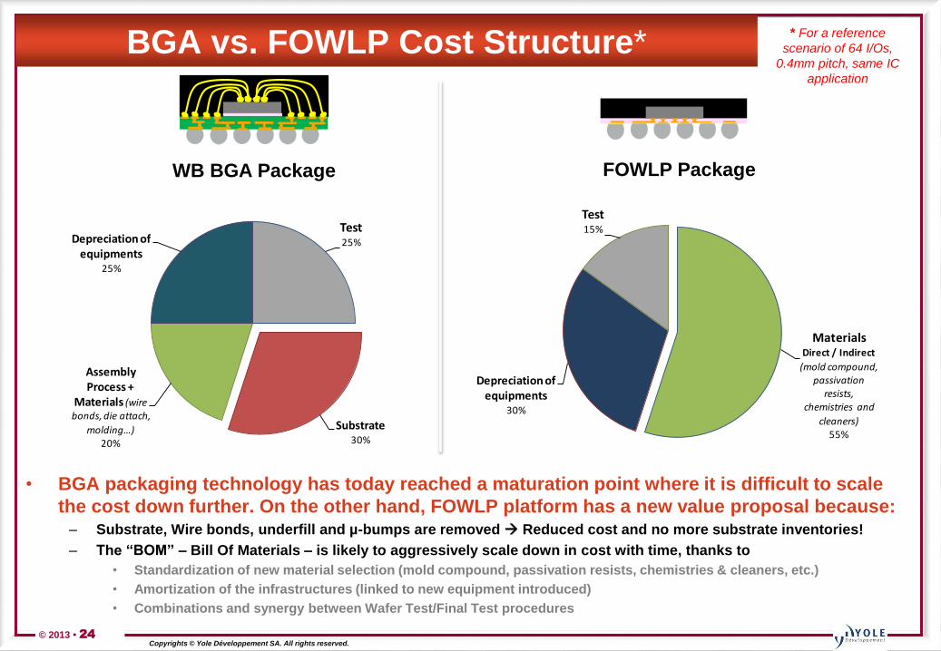
BGA vs. FOWLP Cost Structure*
MaterialsDirect / Indirect
(mold compound, passivation
resists, chemistries and
cleaners)55%
Depreciation of equipments
30%
Test15%
FO WLP package - Cost structure scenario in 2010 -
Test25%
Substrate30%
Assembly Process +
Materials (wire bonds, die attach,
molding…)20%
Depreciation of equipments
25%
WB BGA package - Cost structure scenario in 2010 -
• BGA packaging technology has today reached a maturation point where it is difficult to scale
the cost down further. On the other hand, FOWLP platform has a new value proposal because:– Substrate, Wire bonds, underfill and µ-bumps are removed Reduced cost and no more substrate inventories!
– The “BOM” – Bill Of Materials – is likely to aggressively scale down in cost with time, thanks to
• Standardization of new material selection (mold compound, passivation resists, chemistries & cleaners, etc.)
• Amortization of the infrastructures (linked to new equipment introduced)
• Combinations and synergy between Wafer Test/Final Test procedures
* For a reference
scenario of 64 I/Os,
0.4mm pitch, same IC
application
WB BGA Package FOWLP Package
© 2013 • 25Copyrights © Yole Développement SA. All rights reserved.
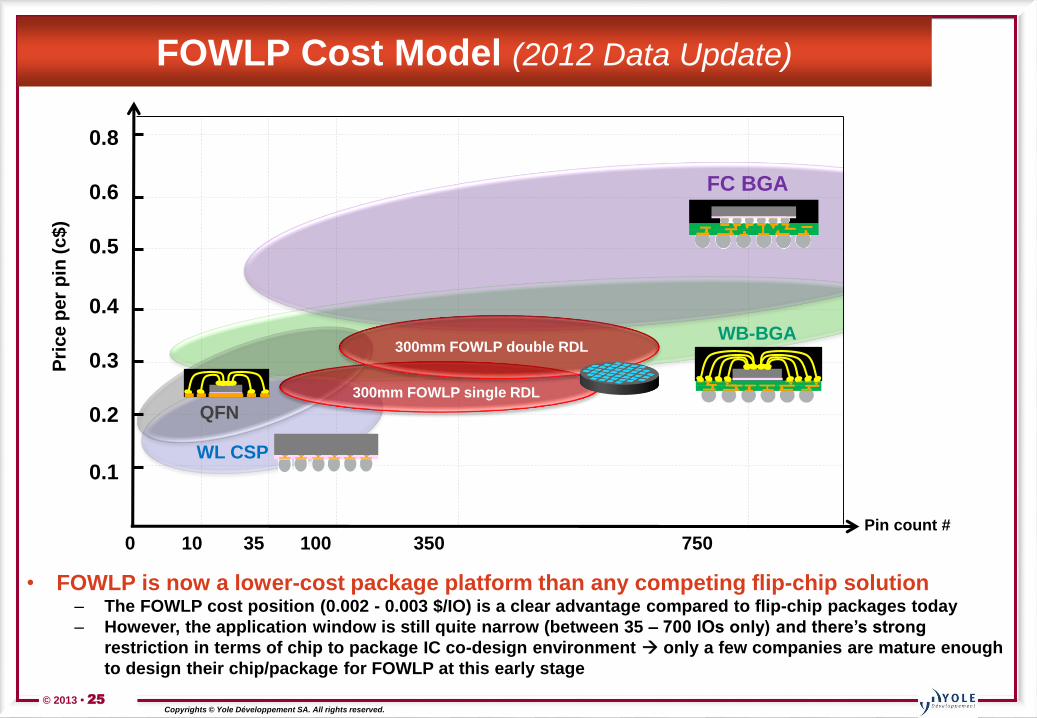
FOWLP Cost Model (2012 Data Update)
WL CSP
0.8
0.6
0.5
0.4
0.3
0.2
0.1
Pri
ce
pe
r p
in (
c$
)
0 10 35 100 350 750 Pin count #
WB-BGA
FC BGA
QFN300mm FOWLP single RDL
300mm FOWLP double RDL
• FOWLP is now a lower-cost package platform than any competing flip-chip solution– The FOWLP cost position (0.002 - 0.003 $/IO) is a clear advantage compared to flip-chip packages today
– However, the application window is still quite narrow (between 35 – 700 IOs only) and there’s strong
restriction in terms of chip to package IC co-design environment only a few companies are mature enough
to design their chip/package for FOWLP at this early stage
© 2013 • 26Copyrights © Yole Développement SA. All rights reserved.
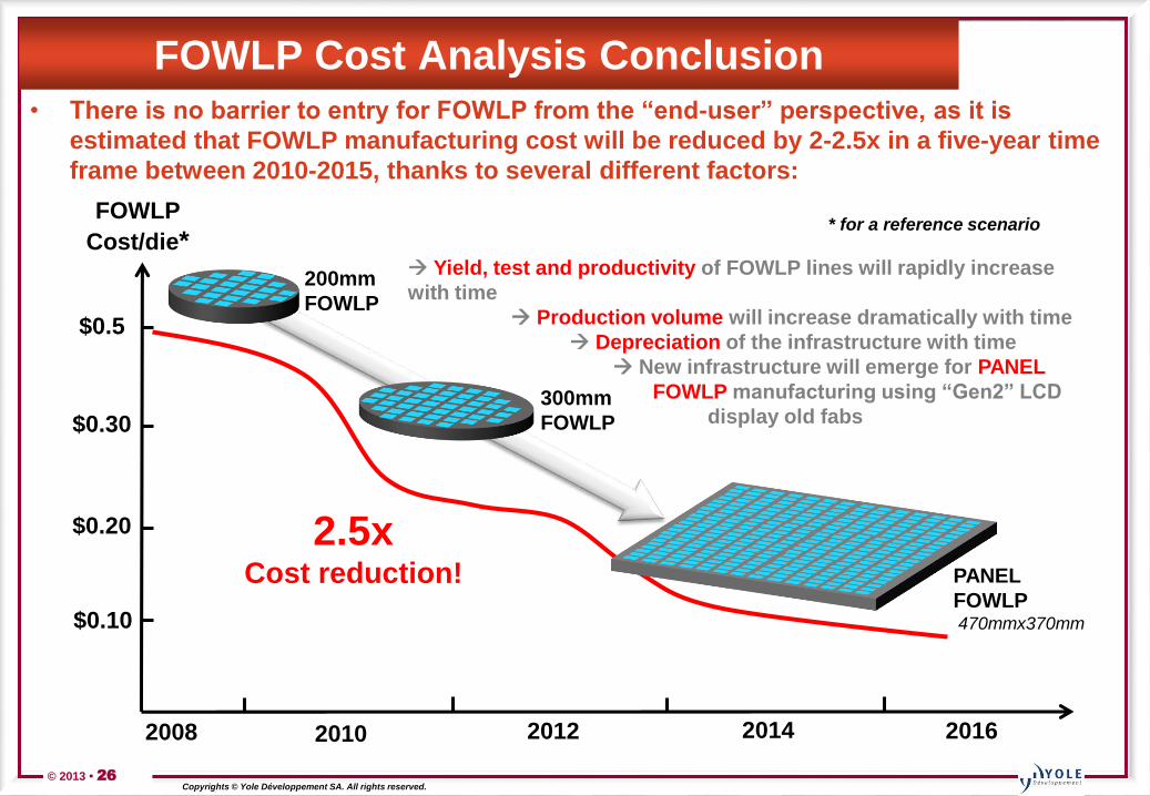
FOWLP Cost Analysis Conclusion
• There is no barrier to entry for FOWLP from the “end-user” perspective, as it is
estimated that FOWLP manufacturing cost will be reduced by 2-2.5x in a five-year time
frame between 2010-2015, thanks to several different factors:
Yield, test and productivity of FOWLP lines will rapidly increase
with time
Production volume will increase dramatically with time
Depreciation of the infrastructure with time
New infrastructure will emerge for PANEL
FOWLP manufacturing using “Gen2” LCD
display old fabs
2010 2012 2014
$0.10
FOWLP
Cost/die*
$0.20
$0.30
$0.5
2016
300mm
FOWLP
PANEL
FOWLP470mmx370mm
200mm
FOWLP
2.5x Cost reduction!
2008
* for a reference scenario
© 2013 • 27Copyrights © Yole Développement SA. All rights reserved.
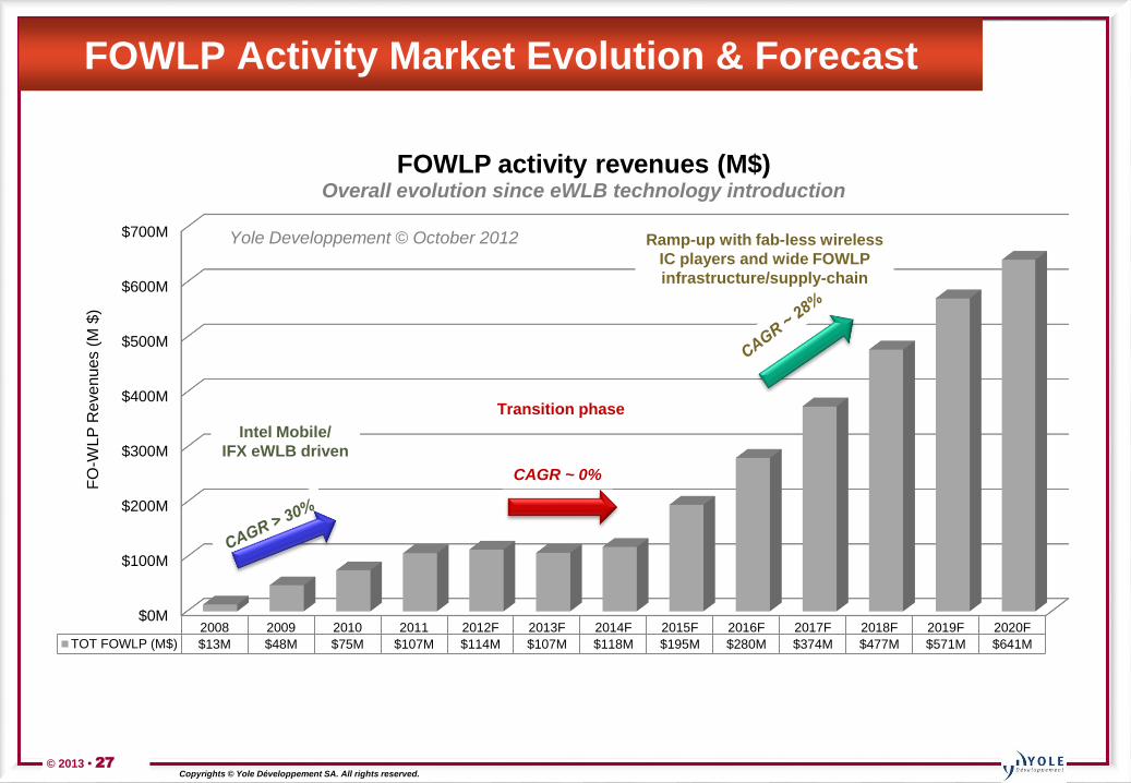
$0M
$100M
$200M
$300M
$400M
$500M
$600M
$700M
2008 2009 2010 2011 2012F 2013F 2014F 2015F 2016F 2017F 2018F 2019F 2020F
TOT FOWLP (M$) $13M $48M $75M $107M $114M $107M $118M $195M $280M $374M $477M $571M $641M
FO
-WL
P R
eve
nu
es (
M $
)
FOWLP activity revenues (M$)Overall evolution since eWLB technology introduction
Yole Developpement © October 2012
FOWLP Activity Market Evolution & Forecast
CAGR ~ 0%
Intel Mobile/
IFX eWLB driven
Transition phase
Ramp-up with fab-less wireless
IC players and wide FOWLP
infrastructure/supply-chain
© 2013 • 28Copyrights © Yole Développement SA. All rights reserved.
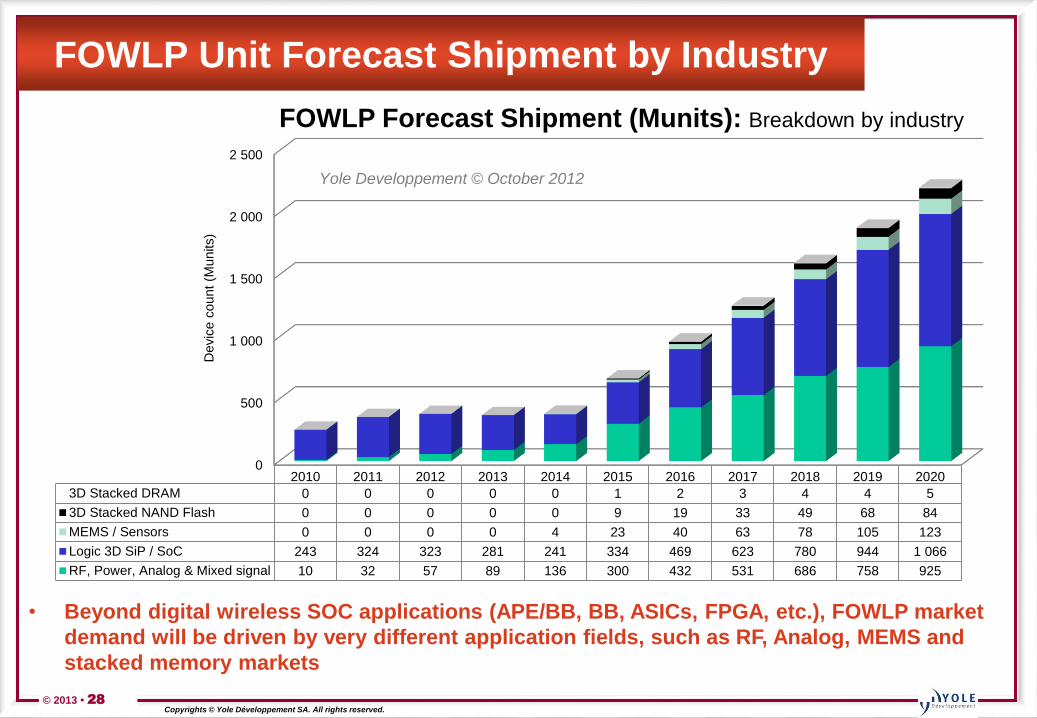
• Beyond digital wireless SOC applications (APE/BB, BB, ASICs, FPGA, etc.), FOWLP market
demand will be driven by very different application fields, such as RF, Analog, MEMS and
stacked memory markets
0
500
1 000
1 500
2 000
2 500
2010 2011 2012 2013 2014 2015 2016 2017 2018 2019 2020
3D Stacked DRAM 0 0 0 0 0 1 2 3 4 4 5
3D Stacked NAND Flash 0 0 0 0 0 9 19 33 49 68 84
MEMS / Sensors 0 0 0 0 4 23 40 63 78 105 123
Logic 3D SiP / SoC 243 324 323 281 241 334 469 623 780 944 1 066
RF, Power, Analog & Mixed signal 10 32 57 89 136 300 432 531 686 758 925
Devic
e c
ount
(Munits)
FOWLP Forecast Shipment (Munits): Breakdown by industry
Yole Developpement © October 2012
FOWLP Unit Forecast Shipment by Industry
© 2013 • 29Copyrights © Yole Développement SA. All rights reserved.
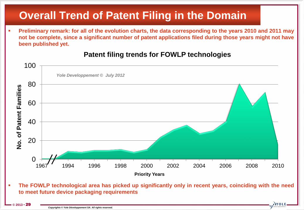
Overall Trend of Patent Filing in the Domain
The FOWLP technological area has picked up significantly only in recent years, coinciding with the need
to meet future device packaging requirements
0
20
40
60
80
100
1967 1994 1996 1998 2000 2002 2004 2006 2008 2010
No
. o
f P
ate
nt
Fam
ilie
s
Priority Years
Patent filing trends for FOWLP technologies
Yole Developpement © July 2012
Preliminary remark: for all of the evolution charts, the data corresponding to the years 2010 and 2011 may
not be complete, since a significant number of patent applications filed during those years might not have
been published yet.
© 2013 • 30Copyrights © Yole Développement SA. All rights reserved.
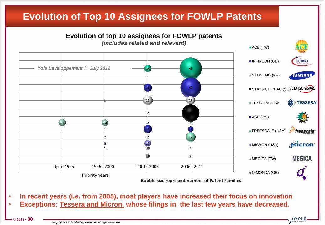
Priority Years
14 41
15 40
1 19 17
2 34
14 13 2 4
1 16 11
2 2 19
2 13
1 8 3
8 3
Evolution of top 10 assignees for FOWLP patents (includes related and relevant)
ACE (TW)
INFINEON (GE)
SAMSUNG (KR)
STATS CHIPPAC (SG)
TESSERA (USA)
ASE (TW)
FREESCALE (USA)
MICRON (USA)
MEGICA (TW)
QIMONDA (GE)
Up to 1995 1996 - 2000 2001 - 2005 2006 - 2011
Evolution of Top 10 Assignees for FOWLP Patents
Bubble size represent number of Patent Families
• In recent years (i.e. from 2005), most players have increased their focus on innovation
• Exceptions: Tessera and Micron, whose filings in the last few years have decreased.
Yole Developpement © July 2012
© 2013 • 31Copyrights © Yole Développement SA. All rights reserved.
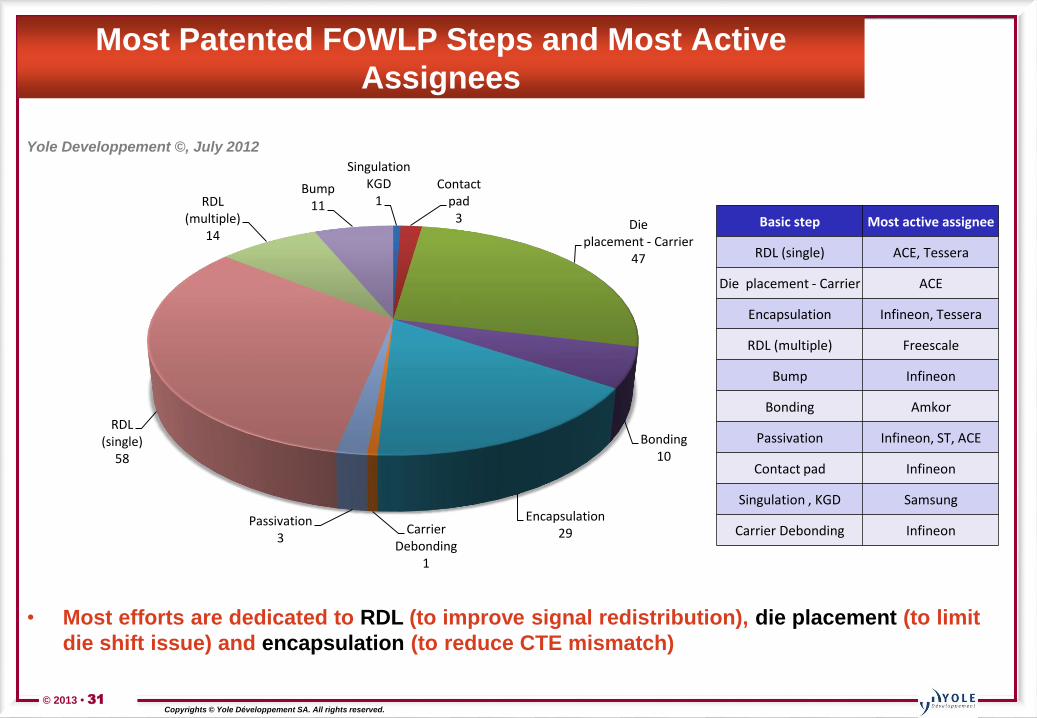
Most Patented FOWLP Steps and Most Active
Assignees
Singulation KGD
1Contact
pad3 Die
placement - Carrier47
Bonding10
Encapsulation29Carrier
Debonding1
Passivation3
RDL(single)
58
RDL(multiple)
14
Bump11
Yole Developpement ©, July 2012
Basic step Most active assignee
RDL (single) ACE, Tessera
Die placement - Carrier ACE
Encapsulation Infineon, Tessera
RDL (multiple) Freescale
Bump Infineon
Bonding Amkor
Passivation Infineon, ST, ACE
Contact pad Infineon
Singulation , KGD Samsung
Carrier Debonding Infineon
• Most efforts are dedicated to RDL (to improve signal redistribution), die placement (to limit
die shift issue) and encapsulation (to reduce CTE mismatch)
© 2013 • 32Copyrights © Yole Développement SA. All rights reserved.
FOWLP Conclusions
FOWLP is a new packaging platform offering new solutions towards integration and miniaturization (10um
line/space, reduced package thickness < 0.5mm, etc.)
FOWLP technology basically extends the concept of wafer scale packaging to many new applications that
are today packaged in BGA and WL CSP packages.
Key applications driving initial FOWLP volume demand will be wireless basebands, RF transceivers and
power management units. Other applications include stacked memories and analog-specific ICs such as
audio codec, MEMS & Sensors, network switches, etc.
A new production infrastructure and opportunity to scale packaging cost down by:
• Increasing wafer diameter (300mm) and moving to PANEL size
• Decreasing importance of material volume in general (as substrate is removed)
• Simplifying the manufacturing infrastructure
• Optimizing supply chain, inventory and cycle times
• Value chain consolidation
Main challenges facing FOWLP are:
• CTE mismatch on bigger package dimensions > 8x8mm (target are 10x10mm, 12x12mm)
• Cost and market acceptance
• Co-design tool implementation
• Manufacturing yield improvements (70% 80% 95-98%)
• Testing approach is yet to be defined (the ultimate goal being to realize the Wafer Test and Final Test in the same
infrastructure)
• Development of “2nd-generation” FOWLP with multi-die and double-side RDL to enter in the 3D SiP dimension
© 2013
Copyrights © Yole Développement SA. All rights reserved.
Thank you!
© 2013• 342013 Copyrights © Yole Développement SA. All right reserved.
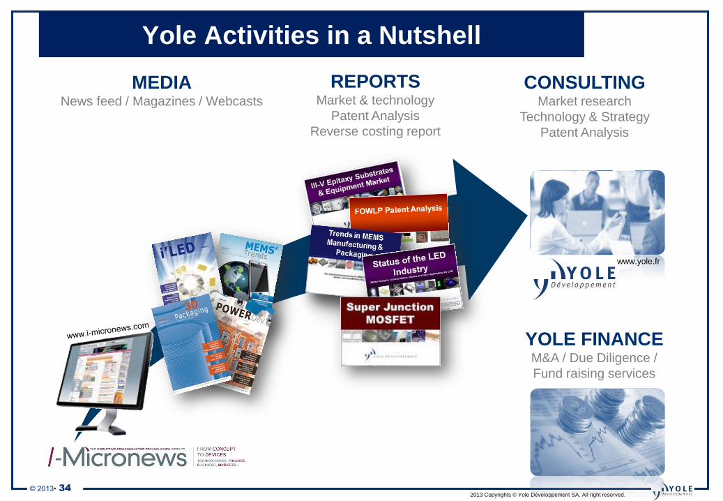
Yole Activities in a Nutshell
MEDIANews feed / Magazines / Webcasts
REPORTSMarket & technology
Patent Analysis
Reverse costing report
CONSULTINGMarket research
Technology & Strategy
Patent Analysis
www.yole.fr
YOLE FINANCE M&A / Due Diligence /
Fund raising services


