

24
CHAPTER 3
SPST BASED POWER OPTIMIZED MULTIPLIER
3.1 INTRODUCTION
Multiplication can be considered as a series of repeated additions.
The number to be added is the multiplicand; the number of times that it is
added is the multiplier; and the result is the product. Each step of addition
generates a partial product. In most computers, the operand usually contains
the same number of bits. When the operands are interpreted as integers, the
product is generally twice the length of operands in order to preserve the
information content. This repeated addition method that is suggested by the
arithmetic definition is slow that it is almost always replaced by an algorithm
that makes use of positional representation. It is possible to decompose
multipliers into two parts. The first part is dedicated to the generation of
partial products, and the second one collects and adds them.
As for adders, it is possible to enhance the intrinsic performance of
multipliers. Acting in the generation part, the booth algorithm is often used
because it reduces the number of partial products. Multiplication occurs
frequently in finite impulse response filters, Fast Fourier transforms, discrete
cosine transforms, convolution, and other important DSP and multimedia
kernels. Owing to the importance of multiplication in DSP and multimedia
applications, several designs have been developed for sub word-parallel
multipliers and Multiply-And-Accumulate (MAC) units. The objective of a

25
good multiplier is to provide a physically compact, good speed and low power
consuming chip.
The basic multiplication principle is two fold:
evaluation of partial products and
accumulation of the shifted partial products
It is performed by the successive additions of the columns of the
shifted partial product matrix. The ‘multiplier’ is successfully shifted and
gates the appropriate bit of the ‘multiplicand’. The delayed, gated instance of
the multiplicand must all be in the same column of the shifted partial product
matrix. They are then added to form the product bit for the particular form.
Multiplication is therefore a multi operand operation. To extend the
multiplication to both signed and unsigned numbers, a convenient number
system would be the representation of numbers in two’s complement format.
Some of the advantages of using two’s complement number system include:
representation of negative numbers in two’s complement
allowing for an easy subtraction function, since – M = M’ + 1
sufficient redundancy allowing for the annihilation of carry or
borrows chains and also, in fact, propagation free addition and
subtraction.
Booth’s recoding technique, used for signed binary numbers
enabling faster multiplications.
3.2 SPURIOUS POWER SUPPRESSION TECHNIQUE (SPST)
The SPST uses a detection logic circuit to detect the effective data
range of arithmetic units, namely adders or multipliers. When a portion of

26
data does not affect the final computing results, the data controlling circuits of
the SPST latch this portion to avoid useless data transitions occurring inside
the arithmetic units. Besides, there is a data asserting control realized by using
registers to further filter out the useless spurious signals of arithmetic unit
every time when the latched portion is being turned on. This asserting control
brings evident power reduction. Figure 3.1 shows the five cases of a 16-bit
addition in which the spurious switching activities occur (Chen et al 2006).
The data are separated into the Most Significant Part (MSP) and the Least
Significant Part (LSP). To know whether the MSP affects the computation
results or not, the detection logic unit is used to detect the effective ranges of
the inputs. The Boolean logical equations from 3.1 to 3.6 given below express
the behavioral principles of the detection logic unit in the MSP circuits of the
SPST-based adder/subtractor:
AMSP = A [15:8]; B MSP = B [15:8]; (3.1)
Aand = A [15].A [14]……A [8]; (3.2)
Band = B [15].B [14]……B [8]; (3.3)
Anor = A [15] + A [14] + …+A[8] ; (3.4)
_____________________
Bnor = B [15] + B [14] + …+B[8] ; (3.5)
____________________
Close = (Aand + Anor). (Band + Bnor) (3.6)
Where ‘A[m]’ and ‘B[n]’ respectively denote the mth
bit of the
operands, A and the nth
bit of the operand ‘B’ and ‘AMSP’ and ‘BMSP’
respectively denote the MSP parts, i.e. the 9th
bit to the 16th bit, of the
operands ‘A’ and ‘B’. When the bits in ‘AMSP, and/or those in ‘BMSP’ are all
one, the value of Aand and/or that of Band respectively become one, while the
bits in AMSP and/or those in BMSP are all zeros, the value of ‘Anor’ and/or that

27
of ‘Bnor’ respectively turn into one. Being one of the three outputs of the
detection logic unit, close
Figure 3.1 Five Cases of 16-bit Addition
denotes whether the MSP circuits can be neglected or not. When the two input
operand can be classified into one of the five classes as shown in Figure 3.1,
the value of close becomes zero which indicates that the MSP circuits can be
closed (Chen et al 2005). Figure 3.1 also denotes that it is necessary to
compensate the sign bit of computing results. Accordingly, the Karnaugh
maps are derived leading to the Boolean equations (3.7) and (3.8) for the
Carr_ ctrl and the sign signals, respectively. In equations (3.7) and (3.8), CLSP
denotes the carry propagated from the LSP circuits:
Carr_ctrl = (CLSP .Aand. Band).(Aand+Anor)(Band +Bnor) (3.7)
Sign = CLSP. (Aand+ Band) + CLSP .Aand. Band (3.8)

28
3.2.1 Proposed Spurious Power Suppression Technique
Figure 3.2 showcases a 16-bit adder/subtractor design based on the
proposed SPST. This example, the 16-bit adder/subtractor, is divided into
MSP and LSP at the place between the 8th
bit and the 9th
bit. Latches
implemented by simple AND gates are used to control the input data of the
MSP. When the MSP is required to produce the result, the input data of MSP
remain the same as usual. When the MSP is not required to produce the result,
the input data of the MSP become zeros to avoid switching power
consumption. From the derived Boolean equations (3.1) to (3.8), the detection
logic unit of the SPST is designed as shown in Figure.3.2 which can
determine whether the input data of MSP should be latched or not. Moreover,
the three 1-bit data is added to control the assertion of the close, sign, and
Carr-ctrl signals in order to further decrease the glitch signals occurring in the
cascaded circuits. These circuits are usually adopted in VLSI architectures
designed for video coding.
Figure 3.2 16-Bit Adder/Subtractor Design Example

29
The SPST uses a detection logic circuit to detect the effective data
range of arithmetic units, e.g., adders or multipliers. When a portion of data
does not affect the final computing results, the data controlling circuits of the
SPST latch this portion to avoid useless data transitions occurring inside the
arithmetic units. Besides, there is a data asserting control realized by using
registers to further filter out the useless spurious signals of arithmetic unit
every time when the latched portion is being turned on. This asserting control
brings appreciable power reduction. In Figure 3.2, SPST is illustrated through
a low power adder/subtractor design example. The adder subtractor is divided
into two parts, MSP and the LSP. The MSP of the original adder/subtractor is
modified to include
1. detection logic circuits
2. data controlling circuits
3. sign extension circuits and
4. logics for calculating carry in and carry out signals
The most important part of this thesis is the design of the control
signal asserting circuits, denoted as asserting circuits in Figure 3.2. Although
this asserting circuit brings sufficient power reduction, it may induce
additional delay. There are two main approaches for the control signal
assertion circuits. They are (1) using registers and (2) using AND gate
3.2.2 Control Signal Assertion Circuit using Registers
The first implementing approach of control signal assertion circuit
using registers is exhibited in Figure 3.3. The three output signals of the
detection logic are

30
1. Close
2. Carr-ctrl and
3. Sign
The three output signals of the detection logic unit are given a
certain amount of delay before they assert. This is demonstrated in the timing
diagram shown in Figure 3.4.
Figure 3.3 Control Signal Assertion Circuit using Registers
Figure 3.4 Timing Diagram for Control Signal Assertion Circuit using
Registers
31
The delay , used to assert the three output signals must be set in
the range of < < , where denotes the data transient period and
denotes the earliest required time of all the inputs. This will filter out the
glitch signals as well as keep the computation results correct. The restriction
that must be greater than to guarantee the registers from latching the
wrong values of control usually decreases the overall speed of the applied
designs. This issue is noticed in high-end applications which demand both
high speed and low power requirements. To solve this problem the other
implementing approach of control signal assertion circuit using AND gate is
adopted.
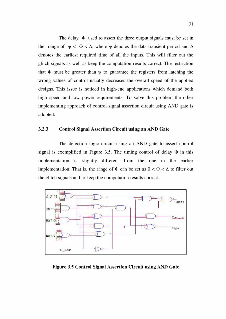
3.2.3 Control Signal Assertion Circuit using an AND Gate
The detection logic circuit using an AND gate to assert control
signal is exemplified in Figure 3.5. The timing control of delay in this
implementation is slightly different from the one in the earlier
implementation. That is, the range of can be set as 0 < < to filter out
the glitch signals and to keep the computation results correct.
Figure 3.5 Control Signal Assertion Circuit using AND Gate

32
This feature allows the upper level system to assert the close signal
with an arbitrarily short delay closing to the positive edge of the clock signal.
This will provide a more flexible controlling space for the delay . When
speed is seriously concerned, this approach has an extremely high flexibility
by adjusting the data asserting time of the SPST equipped multipliers.
Therefore the proposed advanced SPST can benefit multipliers on both high
speed and low power features.
3.2.4 Comparison
The asserting circuit using AND gate achieves a significant
improvement in speed. It has been found that when implemented with AND
gate, the asserting circuits take the less timing delay and require less power
than when implemented using registers. For the latest Xilinx, Spartan 2
family, has been found that the gate delay for the asserting circuit using AND
gate is 13.507ns, while it is 24.107ns r using registers. The power dissipation
for asserting circuit using AND gate is 3mw while for using register it is
4mw. So the asserting circuit using AND gate is chosen for SPST
implementation. The results are compared in Table 3.1 and based on the
comparison in asserting circuit using AND gate is selected for low power
design.
Table 3.1 Comparison of Asserting Circuits
S.NOAsserting
circuit usingVendor Device
Estimated
delay (ns)
Power
dissipation
(mW)
1 Registers Xilinx Sparton 2 24.107 4
2 AND gate Xilinx Sparton 2 13.507 3

33
3.3 MODIFIED BOOTH MULTIPLIER
In order to achieve high-speed multiplication, multiplication
algorithms using parallel counters, such as the modified Booth algorithm has
been proposed (Booth 1951) and some multipliers based on the algorithms
have been implemented for practical use. This type of multiplier operates
much faster than an array multiplier for longer operands because its
computation time is proportional to the logarithm of the word length of
operands. The modified Booth multiplier on the processor is a major source of
energy consumption for Digital Signal Processing programs. Given a pair of
values to be multiplied, power should be reduced if the value is put in with the
lower recoding weight into the second input of the modified Booth multiplier.
Booth multiplication is a technique that allows for smaller, faster
multiplication circuits, by recoding the numbers that are multiplied. It is the
standard technique used in chip design, and it provides significant
improvements over the "long multiplication" technique. First, the "shift and
add", or normal "long multiplication” multiplier design is briefly reviewed.
3.3.1 Reduction of Partial Products: The Modified Booth Coding
It is possible to reduce the number of partial products by half, by
using the technique of radix 4 Booth recoding. The basic idea is that, instead
of shifting and adding for every column of the multiplier term and multiplying
by 1 or 0 for second column, multiply by ±1, ±2 or 0 to obtain the same
results. So, to multiply by 7, (-1), multiply the partial product aligned
against the least significant bit by -1, and multiply the partial product aligned
with the third column by 2:

34
Partial Product 0 = Multiplicand × -1, shifted left 0 bits (x -1)
Partial Product 1 = Multiplicand × 2, shifted left 2 bits (x 8)
This yields the same result as the equivalent shift and add method:
Partial Product 0 = Multiplicand × 1, shifted left 0 bits (x 1)
Partial Product 1 = Multiplicand × 1, shifted left 1 bits (x 2)
Partial Product 2 = Multiplicand × 1, shifted left 2 bits (x 4)
Partial Product 3 = Multiplicand × 0, shifted left 3 bits (x 0)
The advantage of this method is the halving of the number of
partial products. This is important in circuit design as it relates to the
propagation delay in the running of the circuit, the complexity and power
consumption of its implementation.
It is also important to note that there is comparatively little
complexity in multiplying by 0, 1 or 2. All that is needed is a multiplexer or
equivalent, which has a delay time that is independent of the size of the
inputs. Negating 2's complement numbers has the added complication that
needs to add a "1" to the LSB, but this can be overcome by adding a single
correction term with the necessary "1"s in the correct positions.
3.3.2 Radix – 4 Modified Booth Recoding
In partial product reduction step of multiplier, the Booth recoding is
technique is used. In this technique, recoding is applied to multiplier term, in
which three bits in blocks are considered, such that each block overlaps the
previous block by one bit. Grouping starts from the LSB, and the first block
only uses two bits of the multiplier (since there is no previous block to
overlap). Figure 3.6 depicts the grouping of bits from the multiplier term for
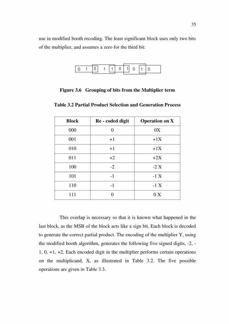
35
use in modified booth recoding. The least significant block uses only two bits
of the multiplier, and assumes a zero for the third bit:
Figure 3.6 Grouping of bits from the Multiplier term
Table 3.2 Partial Product Selection and Generation Process
Block Re - coded digit Operation on X
000 0 0X
001 +1 +1X
010 +1 +1X
011 +2 +2X
100 -2 -2 X
101 -1 -1 X
110 -1 -1 X
111 0 0 X
This overlap is necessary so that it is known what happened in the
last block, as the MSB of the block acts like a sign bit. Each block is decoded
to generate the correct partial product. The encoding of the multiplier Y, using
the modified booth algorithm, generates the following five signed digits, -2, -
1, 0, +1, +2. Each encoded digit in the multiplier performs certain operations
on the multiplicand, X, as illustrated in Table 3.2. The five possible
operations are given in Table 3.3.
36
Table 3.3 Five Possible Operations
Re-coded
digit
Operation on X
0 Add 0 to the partial product
+1 Add X to the partial product
+2 Shift left X one position and add it to the partial
product
-2 Add two’s complement of X to the partial product
-1 Take two’s complement of X and shift left one
position
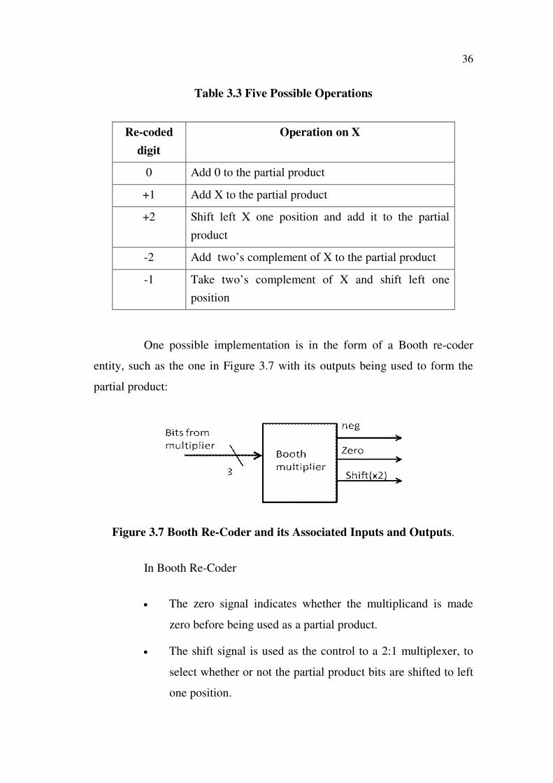
One possible implementation is in the form of a Booth re-coder
entity, such as the one in Figure 3.7 with its outputs being used to form the
partial product:
Figure 3.7 Booth Re-Coder and its Associated Inputs and Outputs.
In Booth Re-Coder
The zero signal indicates whether the multiplicand is made
zero before being used as a partial product.
The shift signal is used as the control to a 2:1 multiplexer, to
select whether or not the partial product bits are shifted to left
one position.

37
Finally, the negative signal indicates whether or not to invert
all of the bits to create a negative product (which must be
corrected by adding "1" at some later stage).
The described operations for booth recoding and partial product
generation can be expressed in terms of logical operations if desired. But, for
synthesis, it is found to be better to implement the tables in terms of VHDL
case and if/then/else statements.
3.4 PROPOSED HIGH SPEED LOW POWER MULTIPLIER
DESIGN
The proposed high speed low power multiplier is designed by
equipping the SPST on a tree multiplier. There are two distinguished design
considerations in designing the proposed multiplier. They are
1. Applying the SPST on the modified Booth encoder.
2. Applying the SPST on the compression tree.
3.4.1 Applying the SPST on the Modified Booth Encoder
Figure 3.8 shows a computing example of Booth multiplying two
numbers “2AC9” and “006A”. The shadow denotes that the numbers in this
part of Booth multiplication are all zero so that this part of the computations
can be neglected. Saving those computations can significantly reduce the
power consumption caused by the transient signals. Based on the analysis on
multiplication, the SPST-equipped modified-Booth encoder, which is
controlled by a detection unit, is proposed.

38
Figure 3.8 An Example of Booth Multiplying Two Numbers
The detection unit has one of the two operands as its input to decide
whether the Booth encoder calculates redundant computations. As shown in
Figure 3.9, the latches can, respectively, freeze the inputs of MUX-4 to MUX-
7 or only those of MUX-6 to MUX-7 when the PP4 to PP7 or the PP6 to PP7
are zero, to reduce the transition power dissipation.
Figure 3.9 SPST Equipped Modified Booth Encoder

39
3.4.1.1 Partial Product Generation
In order to reduce the number of partial products by half, the
technique of radix 4 Booth recoding is used. The basic idea is that, instead of
shifting and adding for every column of the multiplier term and multiplying
by 1 or 0, the second column is multiplied by ±1, ±2, or 0, to obtain the same
results. To Booth recode the multiplier term, consider the bits in blocks of
three, such that each block overlaps the previous block by one bit. Grouping
starts from the LSB, and the first block only uses two bits of the multiplier
(since there is no previous block to overlap). The least significant block uses
only two bits of the multiplier, and assumes a zero for the third bit. The
overlap is necessary so that its shows what happened in the last block, as the
MSB of the block acts like a sign bit. Each block is decoded to generate the
correct partial product. Figure 3.10 presents the booth partial product
generation circuit. It includes AND/OR/EX-OR logic.
Figure 3.10 Booth Partial Product Selector Logic

40
3.4.1.2 Addition of Partial Products
In order to add the partial products that are generated by the
modified booth encoder, the SPST adder is proposed. The operands are
divided into two parts as the Most Significant Part (MSP) and the Least
Significant Part (LSP). The SPST uses a detection logic circuit to detect the
effective data range of arithmetic units, e.g., adders or multipliers. When a
portion of data does not affect the final computing results, the data controlling
circuits of the SPST latch this portion to avoid useless data transitions
occurring inside the arithmetic units. Besides, there is a data asserting control
realized by using registers to further filter out the useless spurious signals of
arithmetic unit every time when the latched portion is being turned on. This
asserting control brings sufficient power reduction. In SPST adder in order to
perform the normal addition the full adder circuit is used.
3.4.1.3 Full Adder Circuit
Full adder is a one-bit adder which represents a basic building
block for all the more elaborate addition schemes. A full adder has three input
signals and two output signals. The input signals consist of the two operands
to be added and the carry input signal from the previous stage. The output
signals are the sum and carry out signals. The truth table for a full adder
circuit is given in Table 3.4. Operations of a full adder are defined by the
Boolean equations for the sum and carry signals.
The Boolean equations for the sum and carry out signals are given
in equation (3.9) and (3.10) respectively:
Si = Ai Bi Cin (3.9)
Ci+1=Ai . Bi + Cin. Ai + Cin. Bi (3.10)

41
Table 3.4 Truth Table for a Full Adder Circuit
Ai Bi Carry in
(Cin)
Sum (Si) Carry out
(Ci+1)
0 0 0 0 0
0 0 1 1 0
0 1 0 1 0
0 1 1 0 1
1 0 0 1 0
1 0 1 0 1
1 1 0 0 1
1 1 1 1 1
Where Ai, Bi are the input operand to be added in the ith
stage and Cin
is the carry from the previous stage. Si is the sum of ith
stage and Ci+1 is the
carry out to the next stage. From the above equation it is possible to
understand that the realization of the sum functions requires two XOR logic
gates. The Carry function is further rewritten defining the Carry-Propagate Pi
and Carry-Generate Gi terms. The Boolean expression for Carry-Propagate Pi
and Carry-Generate Gi terms are given in equations (3.11 and (3.12)
respectively:
Pi = Ai Bi (3.11)
Gi = Ai . Bi (3.12)
At a given stage i, a carry is generated if Gi is true (i.e. both Ai and
Bi are ONEs), and if Pi is true, the stage propagates an input carry to its output
(i.e. either Ai or Bi is ONE). The logical implementation of the full adder is
shown in Figure 3.11.

42
Figure 3.11 Full Adder Implementation
3.4.2 Applying the SPST on the Compression Tree
The proposed SPST-equipped multiplier is illustrated in Figure
3.12. The PP generator generates five candidates of the partial products, i.e.
{-2A, -A, 0, A, 2A}. These are then selected according to the Booth
encoding results of the operand B. When the operand besides the Booth
encoded one has a small absolute value, there are opportunities to reduce the
spurious power dissipated in the compression tree. According to the
redundancy analysis of the additions, the adders are replaced in compression
tree of the multiplier with the SPST-equipped adders, which are marked with
oblique lines.

43
Figure 3.12 SPST- Equipped Multiplier
3.4.2 Flow Chart
The flow chart of power optimization algorithm for the proposed
SPST equipped multiplier is shown in Figure 3.13. In the first step, the HDL
code for conventional array multiplier and the proposed multiplier is written.
Then the functional verification of both multipliers is ensured with the help of
Model-Sim software tool. After checking the functional verification, the
synthesis process is started by using Xilinx tool. During the synthesis, process
power, delay and area reports are generated. The synthesis reports conclude
that the proposed algorithm consumes less power, lower delay and area
reduction because the modified booth encoding is used to reduce the partial
product. In this regard, SPST is used in adder section for minimizing
unwanted addition.

44
Figure 3.13 Power Optimization Algorithm (Continued)

45
Figure 3.13 Power Optimization Algorithm

46
3.5 SIMULATION RESULTS
In the power optimization method the performance of the proposed
high speed low power multiplier is evaluated by comparing this design with a
conventional array multiplier. Both multipliers can be implemented using
VHDL coding. In order to get the power report and delay report, these
multiplier circuits are synthesized using Xilinx software.
3.5.1 Array Multiplier
The main module of the array multiplier is the array 4 entity. Here
“x” and “y” are the four bit input vectors and “p” is the eight bit output
vector.
Figure 3.14 Simulation Result for Array Multiplier
The two 4 bit input values are forced and their s corresponding
results of 8 bits are obtained in Figure 3.14.

47
3.5.2 Proposed High Speed Low Power Multiplier
The main module of the proposed high speed low power multiplier
is designed by using modified booth algorithm. Here the main module uses
three packages, namely the partial product generation, SPST adder, and Full
adder. The simulation result for the partial product generation using modified
booth encoder is represented in Figure 3.15. The simulation results for 4 x 4
high speed low power multiplier using SPST is arrayed in Figure 3.16.
Figure 3.15 Simulation Results for Partial Product Generator
Figure 3.16 Simulation Results for 4x4 Low Power Multiplier

48
Figure 3.17 shows the simulation results for the 16 x 16 high speed
low power multiplier using SPST. In this input A is the 16 bit multiplicand
vector and input B is the 16 bit multiplier vector, while the output is the
product of 16 x 16 Multiplier.
Figure 3.17 Simulation Result for the 16 X 16 Low Power Multiplier
3.5.3 Synthesis Report
The proposed high speed low power multiplier achieves a
significant improvement in speed and power dissipation. It has been found
that the high speed low power multiplier using SPST takes less time delay and
requires less power than array multiplier. For the latest Xilinx, Spartan 2
family, it has been found that the time delay for the high speed low power
multiplier using SPST is 14.886 ns, while it is 21.068 ns for array multipliers.
The power dissipation for high speed low power multiplier using SPST is
35mW while it is 44 mW for array multipliers. The results are summarized in
Table 3.5.

49
Table 3.5 Comparison of Multipliers
S.NO Multiplier type Vendor DeviceEstimated
delay (ns)
Power
dissipation(mW)
1. Array multiplier XilinxSparton
221.068 44
2.
Proposed high
speed low power
Multiplier
XilinxSparton
214.886 35
In this approach, the reduced power and delay of the low power
Multiplier using SPST on modified booth encoders are evaluated. This design
is verified using VHDL behavioral simulation. The SPST equipped
multipliers using AND gates save about 20.45 % power dissipation and they
having 29.3% more speed than the array multiplier.
3.6 SUMMARY
In the power optimization technique delineated so far, the low
power multiplier is designed by equipping the SPST on a modified Booth
encoder which is controlled by a detection unit using an AND gate. The
modified booth encoder will reduce the number of partial products generated
by a factor of 2. The SPST adder avoids the unwanted addition and thus
minimizes the switching power dissipation. The SPST multiplier
implementation with AND gates shows an extremely high flexibility on
adjusting the data asserting time. This facilitates the robustness of SPST to
attain 29.3% speed improvement and 20.45% power reduction when
compared with the conventional multipliers. This design can be verified using
Modelsim 6.5 using VHDL coding and power delay estimated using Xilinix
software.


