

Clock and Data Recovery for SerialDigital Communication
focusing on bang-bang loop CDR design methodology
ISSCC Short Course, February 2002
Rick Walker
Agilent Laboratories
Palo Alto, California

Outline
• Overview of serial data communications
• Degradation mechanisms, data coding
• Jitter measurements
• Clock recovery methods
• Linear PLL review and components
• BB PLL theory
2

Diversity of CDR applications
3
CPU CPU CPU CPU
MEM MEM MEM MEM
Crossbar Switch I/O
10G
packetprocessor
CP
U
Backplane
Switch Board
Network Interfacecards 7-12
Network Interfacecards 1-6
Crossbar
10G 10G 10G 10G
CPU-CPU/MemoryLinecard to Router
• Clock and Data Recovery applications span the rangefrom high-volume, low-cost datacom applications tohigh-performance, long-haul telecom applications
• Many different trade-offs tailor each circuit to the target

CDR data rates over time
1988 1990 1992 1994 1996 1998 2000 2002
20M
50M
100M
200M
500M
1G
2G
5G
10G
20G
50G
LeS88
WaL91
LeB92
HuG93(8x)
IsA94
GHW94
PoL94
EWS95(2x)
LYK96(8x)
YaH96(8x)
FMW97(10x)
ChB97(10x)WSY97 GTL99(10x)
WaN99
Lar99
MSS99GSS00a
MPA00
UWK01
RDP01(4x)
Si Bipolar Trend
SiGe Trend
CMOSSi BipolarSiGe
Ser
ial L
ink
Spe
ed
Inte
rnet
Hos
t Cou
nt
20k
50k
100k
200k
500k
1M
2M
5M
10M
20M
50M
Year of Publication (ISSCC)
DNG91
SoA93
HDW96(2x)
WWS92
CMOS Trend
WHK98(4x)_
4
Historical CDR limit
~PCB skinloss limit
(0.05-0.4 fT)
number of CDR retiming phases givien in “()”

10m 20m 50m 0.1 0.2 0.5 1 2 5Link speed per unit diesize [Gb/square-mm]
0.4
0.60.8
1
2
4
68
10
20Li
nk s
peed
per
uni
t Pow
er [G
b/W
att]
WWS92
GHW94EWS95
FMW97ChB97
WHK98
GTL99
UWK01
TX/RX Gb/W and Gb/mm2
1Tb/s in 40W
Circuit power and die size can be system-limiting factors. Gb/W and Gb/mm2 areplotted for complete TX/RX designs published between ISSCC’92 and 2001. Dashedlines represent an agressive chip supporting 1Tb/s in a total of 40W and 1.8cm2.
1Tb/s in 1.8cm
2
0.2
CMOSSi BipolarSiGe
5

Serial data transmission sends binary bits ofinformation as a series of optical or electrical pulses:
0111011000111110011010010000101011101100011111..
The transmission channel (coax, radio, fiber) generallydistorts the signal in various ways:
From this signal we must recover both clock and data
Basic Idea
6

Some Signal Degradation Mechanisms
• AC coupling droop, baseline wander
• Optical pulse dispersion
• Skin / dielectric loss [YFW82, WWS92, FMW97]
• Random noise
• E+O crosstalk
• Intersymbol interference
• Connector discontinuities
7

Coding for Desirable Properties
• DC balance, low disparity
• Bounded run length
• High Coding Efficiency
• Spectral Shaping (eg: reduce BW or DC component)
• Many Variations are Possible!
• Manchester [San82]
• mB/nB [Gri69][Rou76][WiF83] [YKI84] [Pet88]
• Scrambling: SONET, 64b/66b [CCI90]
• CIMT [WHY91], Conservative Code [Ofe89]
8

Bit Error Rate (BER) Testing
• Pseudo-Random-Bit-Sequence (PRBS) is used tosimulate random data for transmission across the link
• PRBS pattern 2N-1 Bits long contains all N-bit patterns
• Number of errored-bits divided by total bits = BER.
• Typical links are designed for BERs better than 10-12
PRBSdata
generatorTX RX
synth
link
PRBSdata
receiver
clock in clock in
9

Eye diagram construction
randomdata TX RX
synth trigger
link
scope
X X
Y
Y
symbol cell (UI)
amplitudedistribution at Y-Y
jitter
Use a precise clock to chop the data
overlay each period onto one plot
into equal periods
10

-3T -2T -T 0 T 2T 3T 4T
-3T -2T -T 0 T 2T 3T 4T
unitinterval
Impulses spaced equally in time (jitter free signal)
Impulses spaced irregularly in time (jittered signal)
Errors treated as discrete samples of continuous time jitter
time
11After Trischitta and Varma: “Jitter in Digital Transmission Systems”
Definition of Jitter

Jitter Measurements
12

Jitter Measurements
• Datacom Style: Ethernet + Fiber Channelbased on time-domain eye diagrams
• Deterministic Jitter
• Random Jitter
• Telecom Style: SONETbased on frequency-domain jitter spectrums
• Jitter Tolerance
• Jitter Transfer
• Jitter Generation
13

Deterministic and Random Jitter
• Random Jitter (RJ)
• data source is simple repetitive “clock-like” pattern.
• RMS jitter is measured at zero crossings of eye-diagram
• measured jitter is mostly due to clock noise
• Deterministic Jitter (DJ)
• data source is complex scrambled data
• pk/pk jitter is measured at zero crossings of eye-diagram
• RJ contribution is subtracted from the measurement
• measured jitter is mostly due to bandwidth limitations in thedata path.
14

Jitter Tolerance Test Setup
sine wavegenerator
retimingcircuit
bit errorrate tester
decisioncircuit
xamp +limiter
datagenerator
FMmodulated
clock
lasertransmitter
opticalreceiver
opticalattenuator
At each frequency, the sinewavemodulation amplitude is increased untilthe BER penalty is equal to thatcaused by 1dB optical attentuation
After Trischitta and Varma: “Jitter in Digital Transmission Systems” 15

SONET Jitter Tolerance Mask
Data Rate f0[Hz] f1[Hz] f 2 [Hz] f 3 [kHz] f t [kHz]
OC-3 155 Mb 10 30 300 6.5 65
OC-12 622 Mb 10 30 300 25 250
OC-48 2.488 Gb 10 600 6000 100 1000
OC-192 10 Gb 10 2400 24000 400 4000
f0 f1 f2 f3 ft
15 UI
1.5 UI
0.15 UI
This point isusually themost difficultfor many designs
Typical measurement data
from SONET SPEC: TA-NWT-000253 Issue 6, Sept. 1990, fig 5-13 16
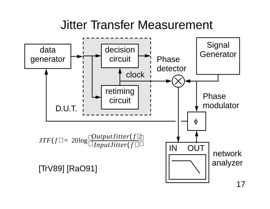
Jitter Transfer Measurement
retimingcircuit
decisioncircuit
datagenerator
networkanalyzer
clock
SignalGenerator
IN OUT
ϕ
Phasedetector
PhasemodulatorD.U.T.
[TrV89] [RaO91]
JTF f( ) 20OutputJitter f( )InputJitter f( )
------------------------------------------ log=
17

Jitter Transfer Specification
fc
P[dB]slope = -20 dB/decade
acceptablerange
Data Rate fc[kHz] P[dB]
155 Mb 130 0.1
622 Mb 500 0.1
2.488 Gb 2000 0.1
This specification isintended to controljitter peaking in longrepeater chains
0dB
18

Jitter Generation
clockcircuit
computeroutputstage
D.U.T.
spectrumanalyzer
generatedclock
19

Jitter Generation (cont.)
cloc
k am
plitu
de
sideband
resu
ltant
∆Θ
1) Measure Jitter Sidebands around Clock
2) Multiply Jitter components by Filter Mask
3) RMS sum total noise voltages over band
4) Convert RMS noise voltage to RMS jitter
Jitterpp rads( ) 2∆Θ= 2Vsideband
Vclock--------------------------
atan≅
OC-48 (2.488 Gb/s SONET) specifies 12 kHz hipass filter,and maximum 0.01 UI RMS integrated jitter.
20

Clock Recovery Concepts
21

NRZ and RZ signallingNRZ = “non return to zero” data
RZ = “return to zero” data
+ + +
+ + +
no clockfrequency inspectrum
clock frequencyappears inspectrum
clock frequency
TNRZ signalling is almost universally used. 22

Spectrum of NRZ data
variations due to DC balance strategy
1 T⁄ 2 T⁄f 0=
pow
er in
dB
2πfT( )sin2π fT
-------------------------
missing clockfrequency
Fc+δFc-δ
23

Filter Method Examples
d dt⁄ X2 bandpass
filter
bandpassfilter
delay
NR
Z D
ata
Inpu
t
Rec
over
ed C
lock
Out
put
e.g.: SAW filter
LC tank
non-linear element
(this last circuit can be thought of as an NRZ-RZ converter)
[Yam80][YTY80][RFC84][Ros84]
[FHH84][AFK87]
24

Summary of Filter Method
Retimed DataJittered NRZ Data Signal
d dt⁄ X2 bandpass
filter/limiter
D Q
Con:
Temperature and frequency variationof filter group delay makes samplingtime difficult to control
Narrow pulses imply high fT
Hi-Q filter difficult to integrate
Pro:
Very simple to implement
Can be built withmicrowave “tinkertoys”using coax to very highfrequencies
τ
25

Q-Factor in resonant circuitsVoltage envelope of ringing circuit falls to 1/sqrt(e) in Qradians.
1.0 1.0/sqrt(e)
Q/2*PI cycles
Fcenter
Q also equals the centerfrequency of a filter divided bythe full-width of the resonancemeasured at the half powerpoints: Fcenter/
ampl
itude
High-Q filter can be emulated by PLL with low loop B.W.26

PhaseDetector
Low-passLoop Filter
VoltageControlledOscillator
DRetimed
DataJittered
Data Signal
PLL
Q
27
Data recovery with simple PLL
Everything in the simple PLL is easily integrable. The remaining problem is tomatch the recovered clock phase to the middle of the data eye. This can bedifficult to achieve over all process variation at very high datarate/ft ratios.

x t( ) A ωcos ct=
x t( ) A ωct φ t( )+[ ]cos=
Perfect Clock:
Jittered Clock:
Practically, is only measured at zero crossings, but istreated as a continuous time signal.
φ t( )
x t( ) φ t( )=
Jitter Signal:
plot of the zero crossingarrival time phase error
After Behzad Razavi: “Monolithic Phase-Locked Loops, ISSCC96 Tutorial” 28
Analytic Treatment of Jitter

PhaseDetector
LoopFilter VCO
Kφ1s---Kv
1 βsτ+( )1 sτ+( )
-----------------------
Warning: Extra integration in VCO complicates the design!
29See Floyd M. Gardner, “Phaselock Techniques”, John Wiley and Sons, for good introduction to PLL theory
Model of linear phase-locked loop

30
Kvs
------Kφ1 βsτ+( )1 sτ+( )
-----------------------a
b
c
c/a c/b
open loop gain
10k 100k 1M 10M 100M 1G 10G1k
0dB
40dB
80dB
-40dB
-80dB
(input jitter)
Linear loop frequency response
(c/a, with loop broken at “X”)

D Qsimplifiedschematicsymbol:
clock
Decision Circuit
• Quantizes amplitude at precise sample instant andtypically uses positive feedback to resolve small inputsignals
• A common choice in bipolar processes is a master/slaveD-flip-flop carefully optimized for input sensitivity and clockphase margin
• To avoid hysteresis in CMOS processes, it is common touse a sense amp which is reset prior to each data sample
31

Example Bipolar Decision Circuit
data in
clock in
Vbias
data out
-5V
master latch slave latch
gnd
• many clever optimizations are possible
[OhT83][Con84][Lai90][Run91][Hau91]
32

VCO alternatives
• [Cor79, Ena87, Wal89, DeV91, Lam93, WKG94]
LC Oscillator Multivibrator Ring Oscillator
Speed Technology Dependent 1-10’s of GHz
Phase Noise Good Poor
Integration Poor
(L, Varactor)
Excellent
Tunability Narrow/Slow Wide/Fast
Stability Good Poor
(needs acquisition aid)
Other Multi-PhaseClocks
After Todd Weigandt, B. Kim, P.Gray, “Timing Jitter Analysis for High-Frequency CMOS Ring Oscillators”, March 10, 199433

Multivibrator VCO
Itune
Capacitor is alternately charged anddischarged by constant current
Tuned by varying Itune in current source
Diode clamps keep output voltageconstant independent of frequency
Relies on non-linear switching foroscillation behavior, and so is limited tomoderate frequencies.
Frequency =I tune
4CVbe-----------------
After Alan B. Grebene, “Analog Integrated Circuit Design”, Van Nostrand Reinhold, 1972, pp 313-315 34

Example Ring Oscillator VCO
Input 1
Input 2
Output
[SyA86][EnA87][Wal89]
Input 1
Tune
Input 2
Tune
Inpu
t 1
Input 2
Output
Output
35

False or Harmonic Locking to Data
36
data
clock
4/3 clock
2x clock
1/2 clock
correct early late correct
early/late indicationscancel in loop filter,leaving an attenuated,but possibly stable locksignal.
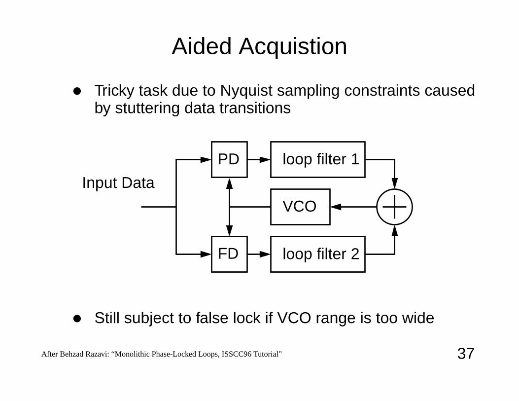
Aided Acquistion
• Tricky task due to Nyquist sampling constraints causedby stuttering data transitions
• Still subject to false lock if VCO range is too wide
PD loop filter 1
loop filter 2FD
VCO
Input Data
37After Behzad Razavi: “Monolithic Phase-Locked Loops, ISSCC96 Tutorial”

Training Loops
1/256
VCO
StateMachine
PDET
FDET
SEL charge pump
Input
Data
Reference Clock flock
dlock
dtransLOS
Clock/256
Clock
2.488GHz/256
divider
bang-bang drive
retimed data
An increasingly common technique is to provide areference clock to the CDR circuit. This allows the VCOprocess-variation to be dynamically trimmed out, avoidingfalse locking problems.
[WSY97]
38

Phase Detectors
• Phase detectors generate a DC component proportionalto deviation of the sampling point from center of bit-cell
• Phase detectors are:
• Binary quantized phase detectors are also called “Bang-bang”, or “early-late” phase detectors
0°
90° 180°
90– °180– °
Continuous
Binary Quantized
After [Hor92]. 39

[Hog85][Shi87]D QD Q
UP
DOWN
Data
1 = Data.................
2= Clock (Early).....
3 = 1 retimed..........
4 = Clock.................
5 = 3 retimed..........
6 = 1 xor 3 (UP).....
7 = 3xor 5 (DOWN)
Data
Clock
“Self-Correcting Phase Detector”
The “Hogge” detector is typical of linear phase detectors. It operates by creatingpulses whose widths are equal to the phase error of the incoming data. Thesepulses may be difficult to produce at high speeds.
40

Early-Late Phase Detector
• NRZ data is sampled at each bit cell and near thetransitions of each bit cell
• Transition sample polarity is compared with preceedingand following bits to deduce the phase error.
• Output is binary quantized, early-late phaseindications, or ternary quantized if a hold-state isimplemented.
A T B
D Q
D Q
D Q
D Q A
T
B
Data
Clock
latchflipflop
A T B Output0 0 0 hold0 0 1 vco fast0 1 0 ?0 1 1 vco slow1 0 0 vco slow1 0 1 ?1 1 0 vco fast1 1 1 hold
[Ale75][WHY91][LaW91][ReG73]
41

BB/charge-pump w/wo hold state
42
timestep [normalized to bit time]
-15-10
-505
1015
jitte
r [n
orm
aliz
ed to
θ BB]
8880 8920 8960 9000
-4
0
4
8
12• hold-mode maintains VCO
frequency when transitionsare absent in the data.
• loop w/o hold has peakjitter run-length timesworse than loop w/hold
loop with hold
w/o hold mode
(simulated with ξ=100,ptransition = 50%)
0 1000 2000 3000 4000 5000 6000 7000 8000 9000 10000

Loop Filters
UP DOWN
VOUT UP DOWN VOUT
0 0 hold
0 1 ramp DOWN
1 0 ramp UP
1 1 hold
[Den88] [Dev91][LaW91] [WuW92]
• should have provision for holding value constantunder long run-length conditions
• may be analog (integrator) or digital (up-downcounter) - but watch out for metastability!
43

Bang-bang PLL Theory
44

Why bother with a BB loop?• it may be difficult to maintain optimum sampling point
with traditional PD/PLL or with filter method overprocess, temperature and supply variation
• Narrow pulses of linear PD’s may not work well atextremely high bit rates
• for monolithic implementation, BB PD has excellentmatch between retiming latch and PD latch - allowsfor operation at highest latch toggle frequency
45D Q
D Q
D Q
D Q A
T
B
data
clk
D Q
PD
filter VCO
data

1988 1990 1992 1994 1996 1998 2000 2002year
8m10m
20m
40m
60m80m0.1
0.2
0.4
0.60.8
ratio
of l
ink
spee
d to
effe
ctiv
e tra
nsit
frequ
ency
LeS88
WBS90
DNG91
LaW91 WWS92
LeB92
HuG93(8x)
SoA93
IsA94
GHW94
PoL94
WBS94
EWS95(2x)LYK96(8x)
YaH96(8x)HDM96(2x)
FMW97(2x)
ChB97(10x)
WSY97
WHK98(4x)GTL99(10x)
WaN99
Lar99
MSS99 GSS00MPA00
UWK01
RDP01(4x)
Linear PLLBB PLL
CDR PLL design style over time
46
BB PLLs have the advantage of precise sample point alignment based on layoutsymmetry. This makes BB PLLs predominate as designs push data rate towardsthe process transit frequency limit. (number of retiming phases shown in ()).

D Q
VCO
• VCO runs at two discrete frequencies: .
• Phase error is evaluated at a discrete time interval. In general, this can be approximated by the
mean transition time of the data.
• A simple D-flip-flop serves as a bb-phase detector iflocking to a clock rather than to a data signal.
f nom f bb±
tupdate
tupdate
47
Simple First Order BB loop

Efficient Simulation Strategy
• Simulating the VCO waveform is unnecessary toaccurately model ideal PLL behavior.
• Only frequency and phase is needed.
• Model all circuit time-varying state variables as voltages.
• Convert between frequency and phase variables withexplicit integration block.
48

Model of First-order Loop
ΣΣ Kvcov td∫
node: Fin ∆F ∆θ1 Θerror bbtune Fvco
unit: Hz Hz UI UI V Hz
φmod
fsample
Fin
49
The tricky bit is to define the loop in terms of an input frequency rather thanan input phase by pulling the VCO integral through the input summation.This allows easy simulation of both frequency and phase steps.

Lock Range for 1st-order loopM
Hz
Deg
rees
time (µseconds)
2490.0
2484.0
5.0 15.0
0.0
-200.0
200.0
vcofreq
phierr
fin
50
Jpp
in lock out of lockout of lock
Fnom f bb+
Fnom
Fnom f bb–
The loop is “locked” whenever the input frequency is bracketed by the twoVCO frequencies. The rapid alternation between frequencies slightly toohigh and slightly too low create a hunting jitter (Jpp).

1st-order loop: locked regionM
Hz
Deg
rees
time (µseconds)
2485.0
2490.0
8.0 12.0
0.0
-40.0
40.0
phierr
finvcofreq
51
The phase detector duty-cycle is proportional to the average frequencyerror.
Fnom f bb+
Fnom
Fnom f bb–

1st-order loop: slew-rate limiting
MH
zD
egre
esD
egre
es
time (µseconds)
2490.0
2486.0
0.0
-200.0
5.0 8.0
0.0
-100.0
fin
vcofreq
dphi1phimod
phierr
52
Although the average input frequency (fin) lies within the lock range of theloop, the added sinusoidal jitter (phimod) causes the instantaneous inputfrequency to exceed the VCO range. The loop phase (dphi1) stopstoggling and goes into slew rate limiting, leading to a phase error (phierr).

Summary of 1st-order loop
• Lock range: .
• Jitter (pk/pk in UI): .
• Bang-bang loop tracking is slew-rate limited. Theeffective loop bandwidth is amplitude dependent.
• The maximum amplitude of phase modulation atfrequency before onset of slew-rate limiting:
.
f nom f bb–( ) f c f nom f bb+( )< <
Jpp 2 t⋅ update= f bb⋅
frequencyoutp
ut ji
tter input is 1UI jitter
0.1UI0.01UI
f modAUI f bb f mod⁄=
53

Summary of 1st-order loop, cont.
• If locked, then the duty cycle , must result in theaverage loop frequency being equal to the inputfrequency ,
• Phase detector average duty cycle , given by
(proportional to ).
C
f cf c f nom ∆f+ C fnom f bb+( ) 1 C–( ) f nom f bb–( )+= =
C12--- ∆f
2 f⋅ bb( )---------------------+
∆f
54

Observations
• Jitter generation, Jitter transfer bandwidth, Jittertolerance and frequency lock range are allinconveniently controlled by one parameter, .
• Phase detector average duty-cycle is proportional tofrequency error.
• Strategy: Use the average duty cycle to control loopcenter frequency. This decouples the lock range fromjitter tolerance/generation giving more design freedom.
• If the center frequency control loop is slow enough, theresulting loop behavior will be very similar to a simplefirst order loop, but with extended frequency lockcapability.
f bb
55

2nd-order BB loop
56
D Q
VCO
1τ--- v td∫
Integral branch
Proportional (BB) branch
Kvco
β
ΣVφ
tupdatepd output
BB path frequency change
BB path phase change
Integrator path frequency change
Integrator path phase change
Vφ
VφβKv
VφβKvt
VφKvt/τ
VφKvt2/2τ

Stability Factor ξ
tupdate (phase change from BB path)
(phase change from integral path)
To quantify the relative independence of the two feedbackloops, take ratio of phase change from BB path to thephase change of the integral path:
ξ∆θbb∆θint-------------≡
βVφKvt
VφKvt2
2τ( )⁄----------------------------------
t tupdate=
2βτtupdate------------------= =
57
VφβKvt
VφKvt2/2τ

Kv
redrawing the 2nd-order loop
ΣΣ v td∫
φmod
fsample
Fin
1τ--- v td∫
β
Σ
Σ Kvv td∫
φmod
FinΣ
fsample
1τ--- v td∫Σ
βKv v td∫
∆F ∆θ1 ∆θ2 ∆θ3
Fint θbb
Vφ
58
Noticing that Vφ is proportional to ∆F, the system can be transformed intoan inner first order bb-loop PLL (in blue) surrounded by an outer low-bandwidth frequency tracking loop (in red).

2nd-order loop: small step in F
time (µseconds)
2490.0
2487.0
0.0
40.0
4.0 7.0
0.0
-2.0
2.0
3 3
1
1
1 1
1
1
1 1
1 1
1 1
Fin
Fint
∆θ1 θbb∆θ3
Vφ
MH
zde
gree
svo
lts
59
A step change in input frequency Fin produces a slow response Fint in theouter, integral loop. The resulting phase error ∆θ1 is tracked by the innerbang-bang loop θbb to produce the final sampler phase error ∆θ3. Noticethat, unlike a linear PLL, there is no jitter accumulation at the sampler.

2nd-order loop: large step in F
time (µseconds)
2500.0
2480.0
0.0
400.0
4.0 7.0
0.0
-2.0
2.0
Fin
Fint
θbb
∆θ3
∆θ1
Vφ
MH
zde
gree
svo
lts
60
In this simulation, the input frequency step is bigger than fbb, so the loopgoes into slew rate limiting, leading to a transient phase error ∆θ3 at thesampler. A fancier loop could detect slew rate limiting by the lack of PDtransitions, and adaptively increase the loop frequency step size.

2nd-order loop: phase jitter tracking
61
time (µseconds)
0.0
-100.0
100.0
0.0
-50.0
50.0
4.0 7.0
0.0
-2.0
2.0
1
1
1 1
12 2
2
2
2
233
3
2
∆θ1
φmod∆θ2
∆θ3θbb
∆θ2
Vφ
degr
ees
degr
ees
volts
Sinusoidal phase jitter φmod is tracked at ∆θ1 with a phase lag by the outer,integral loop. The resulting phase error ∆θ2 is tracked by the inner bang-bangloop θbb to produce the final sampler phase error ∆θ3. The PD output Vφ varieswith the slope of ∆θ2 which is proportional to the instantaneous frequency errorof the outer loop.

2nd-order loop: slope overload
time (µseconds)
0.0
-200.0
200.0
0.0
-100.0
100.0
4.0 7.0
0.0
-2.0
2.0
1
Vφ
∆θ1
φmod∆θ2
∆θ2 ∆θ3
degr
ees
degr
ees
volts
62
θbb
The phase modulation is increased until the instantaneous frequencyerror exceeds the inner loop’s ability to track. Slew-rate limiting atpoint “A” in the inner loop θbb produces a tracking error at thesampler ∆θ3. The loop is designed so that this situation never occursunder normal jitter tolerance conditions.
A

redrawing the 2nd-order loop (again)
Σ Kvv td∫
φmod
FinΣ
fsample
1τ--- v td∫Σ
βKv v td∫Fint θbb
63
ΣFin
t=0,1,2...
Σ
f bb
∆F ∆θ v td∫2 f bb
ξ------------
1st-order ∆Σ
±1v td∫
on ∆F
Transform the loop by pulling the integrators through the summing node “A”.Normalize update interval to 1. Let βKvVφ = fbb Substitute in definition forstability factor ξ. Notice that structure in blue box is a 1st order ∆Σ on ∆F.
A
[Gal94,95]

∆Σ linear system analogy for bb-loop
H(z)Σ Σ
Q(z)X(z) Y(z)
(integration)
Y z( ) H z( )1 H z( )+---------------------X z( ) 1
1 H z( )+---------------------Q z( )+=
gain
freqga
infreq
[Hau91b]
[Gal95]
64

solve for slope overload
Σ 1s---
FinΣ
f bb
∆F ∆θ 2 f bbξ
------------1s---
• Slew rate limiting occurs when |∆F| > fbb
• Maximum input phase modulation in UI, normalized
to ∆θbb is .
• Can be used to compute jitter tolerance.
s2
s2ξ---+ +
s3
s2
+( )⁄
65

slope overload limit vs ξ
1µ 10µ 100µ 1m 10m 0.1 1 10
jitter frequency * tupdate
0.1
10
1k
100k
10M
1G
100G
max
jitte
r be
fore
S.R
.L [n
orm
aliz
ed to
∆θB
B]
ξ=0.1ξ=1
ξ=10
ξ=100ξ=1000
s2
s2ξ---+ +
s3
s2
+( )⁄
simulation
points shownare from numerical
66

jitter generation in frequency-domain
• ∆Σ approximation justifies replacing BB phase detectorwith a noise source.
• Combine total loop phase noise by combining eachphase noise source in RMS fashion.
67
Σ β 1sτ-----+
Kvs
------ ΣΣsourcephasenoise
BB phase noise VCO open loop phase noise
output
of form: Asin(x)/x
H s( )Kvs
------= β 1sτ-----+

example jitter generation calculation
-120-100
-80-60-40-200
-140-130-120-110-100
-90-80
1k 10k 100k 1M 10M 100M 1G-140-130-120-110-100
-90-80
dBdB
c/H
zdB
c/H
z
11 H s( )+--------------------- H s( )
1 H s( )+---------------------
vco phase noise
sourcephase noise
bb phase noise
computed phase noise
measured phase noise
see [WSY97]: fvco=2.488 GHz, fbb = 6 MHz, ξ=32000, tupdate=400ps.68

gaussian jitter generation & gain vs ξ
1m 10m 0.1 1 10 100 1k 10k 100k 1MRMS input jitter [normalized to θBB]
0.1
1
10
100
1k
10k
100k
1M
10MR
MS
out
put j
itter
[nor
mal
ized
toθ B
B]
ξ = 1e-06
ξ = 1e-05
ξ = 1e-04
ξ = 0.001
ξ = 0.01
ξ = 0.1
ξ = 1 Jidle = 0.6+(1.65/ξ)Jlin = 2*Jin/(1+sqrt(ξ))Jwalk = 0.7*sqrt(Jin)Jtot = Jidle + Jlin +Jwalk
ξ = 10
69Simulation is for a non-tristated loop, ptransition = 100%, with 108 timesteps per point. Highstability-factor loops have RMS output jitter equal to the square root of the input jitter!

BB PLL CDR design flowchart
70
Are you using arun-lengthlimited code?
Start
you have the option of usinga loop w/o hold mode, settupdate = max runlength
yes
no
use a loopfilter andVCO with hold mode,set tupdate = tbit
Compute β based on Kvco, Vφ, tupdate,and the jitter generation spec. Checkthat your chosen β will meet the jittertolerance spec. There is a direct tradeoffbetween jitter generation and jittertolerance.
Set the loop-filter time constant τ suchthat the loop stability factor ξ is >> 1 overall process variation.
τ = (tupdate * ξ) / (2β)Typical values of ξ are in the range of100-10,000, based on hold capacitorsize.
Done

Summary
A lot of complexity for a “simple” system...
It’s more of an art than a science
After understanding:
• the components,
• the block diagrams,
• the problems and the attempted solutions,
• and the unique needs for your application,
you’ll be well equipped to craft an artful solution.
71

ReferencesClock and data recovery is a complex field. Any single presentation can only act as an introduction to the field.This eclectic collection of serial data communication references includes papers on signal degradationmechanisms, jitter measurement, phase locked loop design, simulation techniques, multiplexers anddemultiplexers, and coding theory.
Every new application comes with a unique set of constraints and requirements, requiring an artful combination oftechniques to be optimally addressed. I can’t recommend anything better to the newcomer to this field than to readthrough the literature and internalize the many different techniques that exist.
Keywords appear in curly braces {}. Papers in Boldface appear on the short course CDROM in PDF format.
[AFD87] Andrews, G. E., D. C. Farley, S. H. Dravitz, A. W. Schelling, P. C. Davis and L. G. McAfee, A 300Mb/s Clock Recovery andData Retiming System,ISSCC Digest of Technical Papers, 1987, 188-189. {SAW Filter Clock Recovery with emphasis on phasealignment problem}.
[Ale75] Alexander, J. D. H., Clock Recovery from Random Binary Signals,Electronics Letters 11, 22 (30th October 1975), 541-542.{binary quantized phase detector}.
[Arm83] Armitage, C. B., SAW Filter Retiming in the AT&T 432 Mb/s Lightwave Regenerator,Conference Proceedings: AT&T Bell Labs.,Holmdel, NJ, USA, September 3-6, 1984, 102-103. {matches tempco of SAW to tempco of electronics.}.
[Baa86] Baack, C., Optical Wide Band Transmission Systems,CRC Press Inc., 1986. {example of PLL for clock recovery}.[BaD93] Banu, M. and A. Dunlop, A 660Mb/s CMOS Clock Recovery Circuit with Instantaneous Locking for NRZ data and Burst-
Mode Transmission, ISSCC Digest of Technical Papers, February 1993, 102-103. {burst-mode gated VCO}.[BBI94] Boudreau, P. E., W. C. Bergman and D. R. Irvin, Performance of a cyclic redundancy check and its interaction with a data scrambler,
IBM J. Res. Develop. 38, 6 (November 1994), 651-658. {CRC theory Scrambler Error multiplication}[Buc92] Buchwald et al., A., A 6GHz Integrated Phase-Locked Loop using AlGaAs/GaAs Heterojunction Bipolar Transistors,ISSCC Digest
of Technical Papers, 1992, 98,99,253. {Frequency multiplying ring oscillator}.[Byr63] Byrne et al., C. J., Systematic Jitter in Chain of Digital Regenerators,The Bell System Technical Journal, November 1963, 2679.
{clock extraction by filtering}.[Car56] Carter, R. O., Low-Disparity Binary Coding System,Electronics Letters 1, 3 (May, 1956), 67-68. {conditional inversion data encod-
ing disparity}.

[CCI90] CCITT, Digital Line systems based on the synchronous digital hierarchy for use on optical fiber cables,CCITT G.958, 1990.{SONET Payload test patterns regenerator scrambling}.
[ChB97] Chen, D. and M. O. Baker, A 1.25 Gb/s, 460mW CMOS Transceiver for Serial Data Communication,ISSCC Digest of Techni-cal Papers, February 1997, 242- 243,465. {CDR only, 10-phase bang-bang ATB loop, in 6e9 Ft 0.5um CMOS, 12.25 mm^20.460 Watts}.
[Cho92] Chona, F. M. R., Draft Standard, SONET inter-office and intra-office line jitter re.,T1X1.3, May 11, 1992. {Standards SONET jitter}.[Co94] Co, R. S. and J. H. M. Jr., Optimization of Phase-Locked Loop Performance in Data Recovery Systems,IEEE Journal of Solid State
Circuits 29, 9 (September 1994), 1022-1034. {optimum design of CDR loops with linear PD}.[Con84] Connor et al., P. O., A Monolithic Multigigabit/Second DCFL GaAs Decision Circuit,IEEE Electron Device Letters EDL-5, 7
(July 1984), 226-227. {GaAs Fet decision circuit example}.[Cor79] Cordell et al., R. R., A 50MHz Phase and Frequency Locked Loop,IEEE Journal of Solid State Circuits SC-14, 6 (December 1979),
1003-1009. {quadricorrellator phase detector, Tunable LC Oscillator}.[Den88] Den Dulk, R. C., Digital Fast Acquisition Method for Phase-Lock Loops,Electronics Letters 24, 17 (18th August 1988), 1079-1080.
{2 order of magnitude locking speed-up with fancy slip detector & charge pump}.[DeV91] DeVito et al., L., A 52 MHz and 155MHz Clock-Recovery PLL,ISSCC Digest of Technical Papers, February 13-15, 1991, 142, 143,
306. {multivibrator example, Negative resistor chargepump, rotational freq.det.}.[DNG91] DeVito, L., J. Newton, R. Goughwell, J. Bulzacchelli and F.Benkley, A 52MHz and 155 MHz Clock-Recovery PLL,ISSCC
Digest of Technical Papers, February 1991, 142-143,306. {CDR only, 1-phase rotational linear loop, in 3.5e9 Ft Bipolar, 15.028mm^2 0.575 Watts}.
[Dra92] Dravida, S., Error Control Aspects of High Speed Networks,Infocom, 1992, 272-281. {CRC performance with SONET self-synchro-nous scrambler}.
[DR78] D’Andrea, N. A. and F. Russo, A Binary Quantized Digital Phase Locked Loop: A Graphical Analysis,IEEE Transactions on Com-munications COM-26, 9 (September 1978), 1355-1364. {Analysis of BB loop}.
[EnA87] Enam, S. K. and A. A. Abidi, Decision and clock Recovery Circuits for Gigahertz Optical Fiber Receivers in Silicon NMOS,Journalof Lightwave Technology LT-5, 3 (March 1987), 367-372. {MOS tunable monolithic ring oscillator example - Some clever circuitideas for gigabit rates}.
[EnA92] Enam, S. K. and A. A. Abidi, MOS Decision and Clock Recovery Circuits for Gb/s Optical-Fiber Receivers,ISSCC Digest ofTechnical Papers, 1992, 96,97,253. {quadratic phase detector} {MOS decision circuit example}.
[EWS95] Ewen, J. F., A. X. Widmer, M. Soyuer, K. R. Wrenner, B. Parker and H. A. Ainspan, Single-Chip 1062Mbaud CMOS Trans-ceiver for Serial Data Communication,ISSCC Digest of Technical Papers, February 1995, 32-33,336. {TX/RX Mux/demux, 2-phase bang-bang, data samples clock loop, in 6.6e9 Ft 0.45um CMOS, 17.55 mm^2 1.2 Watts}.
[FHH84] Faulkner, D. W., I. Hawker, R. J. Hawkins and A. Stevenson, An Integrated Regenerator for High Speed Optical Fiber TransmissionSystems,IEE Conference Proceedings (November 30 - December 1, 1983) 8-13. {uses rectifier/SAW combo}.
[FLS63] Feynman, R., R. B. Leighton and M. Sands,The Feynman Lectures on Physics, Addison-Wesley Publishing Company, 1963. {Short,simple presentation of timestep simulator for planetary motion, same principles can be used to write a simple pll simulator}.

[FMW97] Fiedler, A., R. Mactaggart, J. Welch and S. Krishnan, A 1.0625Gbps Transceiver with 2x-Oversampling and Transmit SignalPre-Emphasis,ISSCC Digest of Technical Papers 40(February 6-8 1997), 238,239,464. {transmit pre-emphasis, skin loss equal-izer, CDR 1:10 DEMUX, 10-phase bang-bang ATB loop, in 6e9 Ft 0.5um CMOS, 4 mm^2 0.45 Watts}.}.
[Gal94] Galton, I., Higher-order Delta-Sigma Frequency-to-Digital Conversion,Proceedings of IEEE International Symposium on Circuitsand Systems (May 30 - June 2, 1994) 441-444 {Delta-Sigma BB loops phase tracking frequency digitalization PLL}.
[Gal95] Galton, I., Analog-Input Digital Phase-Locked Loops for Precise Frequency and Phase Demodulation,Transactions on Cir-cuits and Systems-II: Analog and Digital Signal Processing42, 10 (October 1995), 621-630. {good discussion of delta-sigmaanalysis of BB PLL’s}.
[Gar79] Gardner, F. M.,Phaselock Techniques, Second Edition, John Wiley and Sons, Inc., 1979. {example of using exor-gate to generateclock component from NRZ data}.
[GHW94] Guo, B., A. Hsu, Y. Wang and J. Kubinec, 125Mb/s CMOS All-Digital Data Transceiver Using Synchronous Uniform Sampling,ISSCC Digest of Technical Papers, February 1994, 112-113. {TX/RX, 1-phase ATB with digital phase adjustment loop, in 3.75e9 Ft0.8um CMOS, 6.38 mm^2 0.175 Watts}.
[Gla85] Glance, B. S., New Phase-Lock Loop Circuit Providing Very Fast Acquistion Time,IEEE Transactions on Microwave Theory andTechniques MTT-33, 9 (September 1985), 747-754. {adds non-linear time constant to speed PLL acquisition by 2 orders of mag.}.
[GMP78] Gruber, J., P. Marten, R. Petschacher and P. Russer, Electronic Circuits for High Bit Rate Digital Fiber Optic Communication Sys-tems, IEEE Transactions on CommunicationsCOM-26, 7 (July 1978), 1088-1098.
[Gol82] Golomb, S. W., Shift Register Sequences,Aegean Park Press, 1982. {classic text on Pseudo-Random sequence generation, ISBN:0-89412-048-4}
[Gri69] Griffiths, J. M., Binary Code Suitable for Line Transmission,Electronics Letters 5, 4 (February 20, 1969), 79-81. {5b/6b encodingexample}.
[GSS00a] Greshishchev, Y. M., P. Schvan, J. L.Showell, M. Xu, J. J.Ojha and J. E. Rogers, A Fully Integrated SiGe Receiver IC for 10Gb/s DataRate,ISSCC Digest of Technical Papers, February 2000, 52-53,447. {CDR DEMUX BIST, 1-phase bang-bang loop, in 50e9 Ft SiGe,20.25 mm^2 4.5 Watts}.
[GSS00b] Greshishchev, Y. M., P. Schvan, J. L. Showell, M. Xu, J. J. Ojha and J. E. Rogers, A Fully Integrated SiGe Receiver IC for 10-Gb/s Data Rate,IEEE Journal of Solid State Circuits35, 12 (December 2000), 1949-1957. {CDR DEMUX BIST, 1- phase bang-bang loop, in 50e9 Ft SiGe, 20.25 mm^2 4.5 Watts}.
[GTL99] Gu, R., J. M. Tran, H. Lin, A. Yee and M. Izzard, A 0.5-3.5Gb/s Low-Power Low-Jitter Serial Data CMOS Transceiver,ISSCCDigest of Technical Papers, February 1999, 352-353,478. {TX/RX MUX/DEMUX BIST, 10-phase bang-bang ATB loop, in10.7e9 Ft 0.28um CMOS, 1 mm^2 0.250 Watts}.
[Gup75] Gupta, S. C., Phase-Locked Loops,Proceedings of the IEEE 63, 2 (February 1975), 291-306. {Good systematic outline survey ofcommunication-type PLL’s}.
[Hau91a] Hauenschild et al., J., A Silicon Bipolar Decision Circuit Operating up to 15Gb/s,IEEE Journal of Solid State Circuits 26, No.11(November 1991), 1734-1736. {Si bipolar decision circuit example}.
[Hau91b] Hauser, M. W., Principles of Oversampling A/D Conversion,J. Audio Eng. So. Vol 39, 1/2 (Jan/February 1991), 3-26. {excellent tuto-rial on Delta Sigma AD, Oversampling, noiseshaping}.

[HDM96] Hauenschild, J., C. Dorshcky, T. W. Mohrenfels and R. Seitz, A 10Gb/s BiCMOS Clock and Data Recovery 1:4-Demultiplexerin a Standard Plastic Package with External VCO,ISSCC Digest of Technical Papers, February 1996, 202-203,445. {CDR 4:1DEMUX, 2-phase bang-bang ATB loop, in 16e9 Ft BiCMOS, 5.29 mm^2.450 Watts}.
[HeS88] Hein, J. P. and J. W. Scott, z-Domain Model for Discrete-Time PLL’s,IEEE Transactions on Circuits and Systems 35, 11 (November1988), 1393-1400. {good discussion of using z-transforms in PLL analysis}.
[Hog85] Hogge, Jr., C. R., A Self Correcting Clock Recovery Circuit,IEEE Transactions on Electron Devices ED-32, 12 (December1985), 2704-2706. {Original Hogge detector, interesting phase detector idea...}.
[Hor92] Hornak, T., Interface Electronics for Fiber Optic Computer Links,Intensive Course on Practical Aspects in Analog IC Design, Lau-sanne, Switzerland, June 29-July 10, 1992. {Excellent overview of components for serial optical data transmission}.
[HuG93] He, T. and P. Gray, A Monolithic 480 Mb/s AGC/Decision/Clock Recovery Circuit in 1.2 um CMOS,IEEE Journal of SolidState Circuits 28, 12 (Dec. 1993) 1314-20 {CDR only, 8-phase linear ATB loop, in 2.4e9 Ft 1.2um CMOS, 9 mm^2 0.9 Watts}.
[IsA94a] Ishihara, N. and Y. Akazawa, A Monolithic 156Mb/s Clock and Data-Recovery PLL Circuit using the Sample-and-Hold Tech-nique, IEEE Journal of Solid State Circuits29, 12 (December 1994), 1566-1571. {CDR only, 1-phase linear 90-degree delayeddata + narrow pulses loop, in 16e9 Ft Bipolar, 8.4 mm^2 0.320 Watts}.
[IsA94b] Ishihara, N. and Y. Akazawa, A Monolithic 156Mb/s Clock and Data-Recovery PLL Circuit using the Sample-and-Hold Technique,ISSCC Digest of Technical Papers, February 1994, 110-111,318. {CDR only, 1-phase linear 90-degree delayed data + narrow pulsesloop, in 16e9 Ft Bipolar, 8.4 mm^2 0.320 Watts}.
[Kas85] Kasper et al., B. L., SAGM Avalanche Photodiode Optical Receiver for 2 Gbit/s and 4 Gbit/s,Electronic Letters 21, 21 (10th October1985), 982-984. {eye diagram}.
[KWG94] Kim, B., T. C. Weigandt and P. R. Gray, PLL/DLL System Noise Analysis for Low Jitter Clock Synthesizer Design,ISCAS proceed-ings, May 30 - June 2, 1994, 31-34. {Excellent and Intuitive discussion of Jitter in Ring Oscillators}.
[Lai90] Lai, B., Decision Circuit Lowers Transmission Bit Error Rates,Microwaves and RF,July 1990, 118- 122. {Si bipolar decision circuitexample}.
[Lam93] Lam, V. M. T., Microwave Oscillator Phase Noise Reduction Using Negative Resistance Compensation,Electronics Letters 29, 4(February 18th, 1993), 379-340. {Leeson negative resistance phase noise second harmonic IC}.
[Lar99] Larsson, P., A 2-1600MHz 1.2-2.5V CMOS Clock- Recovery PLL with Feedback Phase-Selection and Averaging Phase-Inter-polation for Jitter Reduction, ISSCC Digest of Technical Papers, February 1999, 356-357. {CDR only, 1-phase bang- bang withdigital phase shifter loop, in 12e9 Ft 0.25um CMOS, 0.036 mm^2 0.072 Watts}.
[LaW91] Lai, B. and R. C. Walker, A Monolithic 622Mb/s Clock Extraction Data Retiming Circuit,ISSCC Digest of Technical Papers 34(Feb-ruary 13-15, 1991), 144,145. {binary quantized phase detector}.
[LeB92a] Lee, T. H. and J. F. Bulzacchelli, A 155MHz Clock Recovery Delay- and Phase-Locked Loop,ISSCC Digest of TechnicalPapers, February 1992, 160- 161,272. {CDR only, 1-phase rotational linear loop, in 3.5e9 Ft Bipolar, 10.75 mm^2 0.364 Watts}.
[LeB92b Lee, T. H. and J. F. Bulzacchelli, A 155MHz Clock Recovery Delay- and Phase-Locked Loop, IEEE Journal of Solid State Cir-cuits 27, 12 (December 1992), 1736-1746. {CDR only, 1-phase linear 90- degree delayed data + narrow pulses loop, in 16e9 FtBipolar, 8.4 mm^2 0.320 Watts}.

[LeS88] Leonowich, R. H. and J. M. Steininger, A 45-MHz CMOS phase/frequency-locked loop timing recovery circuit,ISSCC Digest ofTechnical Papers, February 1988, 14. {CDR only, 1-phase linear (narrow pulse), rotation frequency detector loop, in 1.65e9 Ft1.75um CMOS, 3 mm^2.250 Watts}.
[LiC81] Lindsey, W. C. and C. M. Chie, A Survey of Digital Phase-Locked Loops,Proceeding of the IEEE 69, 4 (April 1981), 410-431. {Pre-sents a good taxonomy of digital PLLs}.
[LYK96] Lee, I., C. Yoo, W. Kim, S. Chai and W. Song, A 622Mb/s CMOS Clock Recovery PLL with Time- Interleaved Phase DetectorArray, ISSCC Digest of Technical Papers, February 1996, 198-199,444. {CDR DEMUX, 8-phase bang-bang ATB loop, in3.75e9 Ft 0.8um CMOS, 0.72 mm^2 0.200 Watts}.
[Mac87] MacDougall, M. H.,Simulating Computer Systems - Techniques and Tools, The MIT Press, Cambridge, Massachusetts, 1987.{description and source code for event driven simulator}.
[MCC01] Momtaz, A., J. Cao, M. Caresosa, A. Hairapitian, D. Chung, K. Vakilian, M. Green, B. Tan, K. Jen, I. Fujimori, G. Gutierrez,Y. Cai, S. Ueno, K. Watanabe, T. Kato, T. Shinohara, K. Mikami, T. Hashimoto, A. Takai, K. Washio, R. Takeyar and T.Harada, A Single-Chip 10Gb/s Transceiver LSI using SiGe SOI/BiCMOS,ISSCC Digest of Technical Papers, February 2001,82-83,435. {TX/RX MUX/DEMUX BIST, 1-phase linear rotational sample-hold loop, in 90e9 Ft SiGe CMOS, 29.68 mm^2 2.6Watts}.
[McG90] McGaughey, J. T., Convert NRZ format to Biphase,Electronic Design, April 12, 1990, 86. {biphase example}.[MPA00] Meghelli, M., B. Parker, H. Ainspan and M. Soyuer, A SiGe BiCMOS 3.3V Clock and Data Recovery Circuit for 10Gb/s Serial
Transmission Systems,ISSCC Digest of Technical Papers, February 2000, 56-57. {CDR only, 1-phase bang-bang loop, in 45e9Ft, 6 mm^2 0.42 Watts}.
[MSS99] Morikawa, T., M. Soda, S. Shiori, T. Hashimoto, F. Sato and K. Emura, A SiGe Single-Chip 3.3V Receiver IC for 10Gb/s Opti-cal Communication System, ISSCC Digest of Technical Papers, February 1999, 380-381,481. {CDR TIA only, 1-phase linearHogge loop, in 60e9 Ft SiGe, 6 mm^2 0.66 Watts}.
[OFC84] O’Connor, P., P. G. Flahive, W. Clemetson, R. L. Panock, S. H. Wemple, S. C. Shunk and D. P. Takahashi, A Monolithic Multigigabit/Second DCFL GaAs Decision Circuit,IEEE Electron Device Letters EDL-5, 7 (July 1984),. {2.4 GHz ED GaAs Mesfet Flip-flop w/input buffer amp}.
[Ofe89] Ofek, Y., The Conservative Code for Bit Synchronization,IEEE Transactions on Communications, 1989. {conserves transition num-ber, uses divider for clock recovery}.
[OhT83] Ohta, N. and T. Takada, High Speed GaAs SCFL Monolithic Integrated Decision Circuit for Gb/s Optical Repeaters,Electronics Let-ters, September 1983. {GaAs Decision Circuit}.
[Par89] Park et al., M. S., Novel Regeneration Having Simple Clock Extraction and Automatic Phase Controlled Retiming Circuit,ElectronicLetters 25(January 1989), 83-84. {clock extraction by filtering}.
[Pet88] Petrovic, R., Low Redundancy Optical Fiber Line Code,Journal of Optical Communication 9, 3 (1988), 108-111. {13B/14B codedesign}.
[PLS92] Pottbacker, A., U. Langmann and H. Schreiber, A Si bipolar phase and frequency detector IC for clock extraction up to 8Gb/s,IEEEJournal of Solid State Circuits 27, 12 (December 1992), 1747-1751. {linear quadrature phase/frequency detector}.

[PoL94a] Pottbacker, A. and U. Langmann, An 8GHz Silicon Bipolar Clock-Recovery and Data-Regenerator IC,IEEE Journal of SolidState Circuits29, 12 (December 1994), 1572-1576. {CDR only, 1-phase linear loop, in 25e9 Ft Bipolar, 3.06 mm^2 2.25 Watts}.
[PoL94b] Pottbacker, A. and U. Langmann, An 8GHz Silicon Bipolar Clock-Recovery and Data-Regenerator IC,ISSCC Digest of TechnicalPapers, February 1994, 116-117,320. {CDR only, 1-phase linear loop, in 25e9 Ft Bipolar, 3.06 mm^2 2.25 Watts}.
[RaO91] Ransijn, H. and P. O’Connor, A PLL-Based 2.5-Gb/s GaAs Clock and Data Regenerator IC,JSSC 26, 10 (October 1991),1345-1353. {Rotational frequency detector, Limiting Amp, Jitter Transfer Measurement}.
[Raz96a] B. Razavi, ed.,Monolithic phase-locked loops and clock recovery circuits: theory and design, IEEE Press, 1996. {A volume ofselected reprints with bibliography}.
[Raz96b] Razavi, B., Monolithic Phase-Locked Loops,ISSCC Tutorial, San Francisco, CA, February 7, 1996. {Good overview of non-data-driven PLL theory}.
[Raz96c] Razavi, B., A 2.5-Gb/s 15-mW Clock Recovery Circuit,IEEE Journal of Solid State Circuits31, 4 (April 1996), 472-480. {dualloop phase frequency quadricorrelator}.
[RCF84] Rosenberg, R. L., C. Chamzas and D. A. Fishman, Timing Recovery with SAW Transversal Filters in the Regenerators of UnderseaLong-Haul Fiber Transmission Systems,Journal of Lightwave Technology LT-2, 6 (December 1984), 917-925. {discusses jitter accu-mulation}.
[RDP01] Reinhold, M., C. Dorschky, F. Pullela, E. Rose, P. Mayer, P. Paschke, Y. Baeyens, J. Mattia and F. Kunz, A Fully-Integrated40Gb/s Clock and Data Recovery / 1:4 DEMUX IC in SiGe Technology,ISSCC Digest of Technical Papers,February 2001, 84-85,435. {CDR DEMUX, 4-phase ATB loop, in 72e9 Ft SiGe HBT, 9 mm^2 5.4 Watts}.
[ReG73] Reddy, C. P. and S. C. Gupta, A Class of All-Digital Phase Locked Loops: Modeling and Analysis,IEEE Transactions on industrialElectronics and Control Instrumentation IECI-20, 4 (November 1973), 239-251. {discusses of binary-quantized phase detection}.
[RHF90] Ross, F. E., J. R. Hamstra and R. L. Fink, FDDI - A LAN among MANs,ACM Computer Communications Review, July 1990, 16-31.{4b/5b encoding example}.
[RoM77] Roza, E. and P. W. Millenaar, An Experimental 560 MBit/s Repeater with Integrated Circuits,IEEE Transactions on CommunicationsCOM-25, 9 (September 1977),. {coax-based. good comparison of PLL vs filter-type clock extraction}.
[Ros84] Rosenberg et al., R. L., Timing Recovery with SAW Transversal filters in the Regenerators of Undersea Long-haul Fiber Transmis-sion Systems,IEEE Journal of Lightwave Technology LT-2, 6 (December 1984), 917-925. {clock extraction by SAW}.
[Ros85] Ross, F. E., An Overview of FDDI: the Fiber Distributed Data Interface,IEEE Journal on Selected Areas in Communications 7, 7(September 1985), 1046, Table 1. {4b/5b encoding example, example of frame synch characters}.
[Rou76] Rousseau, M., Block Codes for Optical-Fibre Communication,Electronics Letters 12, 18 (2nd September 1976), 478-479. {mBnBcode discussion, run length limits, power spectra, 5b6b recommended}.
[RuG91] Runge, K. and J. L. Gimlett, 20Gb/s AlGaAs HBT Decision Circuit IC,Electronics Letters 27, 25 (5th December 1991), 2376-2378.{GaAs HBT decision circuit example}.
[Run91] Runge et al., K., Silicon Bipolar Integrated Circuits for Multi-Gb/s Optical Communication Systems,IEEE Journal on Selected Areasin Communications 9, 5 (June 1991), 640. {Si bipolar decision circuit example}.
[San82] Sandera, L., Improve Datacomm Links by Using Manchester Code, EDN, February 17, 1982, 155-162. {manchester coding exam-ple}.

[Shi87] Shin et al., D., Selfcorrecting Clock Recovery Circuit with Improved Jitter Performance,Electronics Letters 23, 3 (29th Janu-ary 1987), 110-111. {Improved Hogge detector}.
[SHL99] Scheytt, C., G. Hanke and U. Langmann, A 0.155-, 0.622-, and 2.488-Gb/s Automatic Bit-Rate Selecting Clock and DataRecovery IC for Bit-Rate Transparent SDH Systems,IEEE Journal of Solid State Circuits34, 12 (December 1999), 1935-1943.{quadrature p/f detector, delay-interpolated ring oscillator).
[SoA93] Soyuer, M. and H. A. Ainspan, A Monolithic 2.3 Gb/s 100mW Clock and Data Recovery Circuit,ISSCC Digest of TechnicalPapers, February 1993, 158- 159,282. {CDR only, 1-phase bang-bang data triggered loop, in 30e9 Ft Bipolar, 1.3 mm^2 0.100Watts}.
[SyA86] Syed, K. E. and A. A. Abidi, Gigahertz Voltage Controlled Oscillator,Electronics Letters 22(June 5, 1986), 677-679. {MOS tunablemonolithic ring oscillator example}.
[TrV89] Trischitta, P. R. and E. L. Varma,Jitter in digital transmission systems, Artech House, Inc., 1989. {good overview of jitter (textbook)ISBN 0-89006-248-X}.
[UWK01] Ueno, S., K. Watanabe, T. Kato, T. Shinohara, K. Mikami, T. Hashimoto, A. Takai, K. Washio, R. Takeyar and T. Harada, ASingle-Chip 10Gb/s Transceiver LSI using SiGe SOI/BiCMOS, ISSCC Digest of Technical Papers, February 2001, 82-83,435. {TX/RX MUX/DEMUX BIST, 1-phase linear rotational sample-hold loop, in 90e9 Ft SiGe CMOS, 29.68 mm^2 2.6Watts}.
[Wal89] Walker, R. C., Fully Integrated High Speed Voltage Controlled Ring Oscillator,U.S. Patent 4,884,041, Granted Nov. 28, 1989. {Sibipolar tunable monolithic ring oscillator example}.
[WaN99] Wang, H. and R. Nottenburg, A 1Gb/s CMOS Clock and Data Recovery Circuit,ISSCC Digest of Technical Papers, February1999, 354-355,477. {CDR only, 1-phase analog track-hold + rotational fd loop, in 6e9 Ft 0.5um CMOS, 7.29 mm^2 0.300Watts}.
[WBS90] Wallace, P., R. Bayruns, J. Smith, T. Laverick and R. Shuster, A GaAs 1.5Gb/s Clock Recovery and Data Retiming Circuit,ISSCCDigest of Technical Papers, February 1990, 192-193. {CDR only, 1-phase delay & multiply w/SAW loop, in 20e9 Ft 0.5um GaAsMESFET, 2 mm^2 0.75 Watts}.
[WBS94] Wang, Z., M. Berroth, J. Seibel, P. Hofmann, A. Hulsmann, Kohler, B. Raynor and J. Schneider, 19GHz Monolithic Integrated ClockRecovery Using PLL and 0.3um Gate-Length Quantum-Well HEMTs,ISSCC Digest of Technical Papers, February 1994, 118-119.{CDR only, 1-phase linear xor of data and clock pulses loop, in 50e9 Ft 0.3um HEMT, 1.5 mm^2 0.350 Watts}.
[WHK98] Walker, R. C., K. Hsieh, T. A. Knotts and C. Yen, A 10Gb/s Si-Bipolar TX/RX Chipset for Computer Data Transmission,ISSCC Digest of Technical Papers 41(February 5-7 1998), 302,303,450. {multi-phase architecture, 8-phase VCO, ft-doubleramplifier, bb-loop CDR MUX/DEMUX, 4-phase BB/ATB loop, in 25e9 Ft Bipolar, 28.6 mm^2 8.5 Watts}.}.
[WHY91] Walker, R. C., T. Hornak, C. Yen, J. Doernberg and K. H. Springer, A 1.5Gb/s Link Interface Chipset for Computer Data Transmis-sion,IEEE Journal on Selected Areas in Communications 9, 5 (June 1991), 698-703. {binary quantized phase detector with mastertransition}.
[WiF83] Widmar, A. X. and P. A. Franaszek, A DC Balanced, partitioned-Block 8B/10B Transmission Code,IBM Journal of Research andDevelopment 27, 5 (September 1983), 440-451. {8b/10b encoding example - Precursor to Fiber Channel’s 8B/10B code}.

[WKG94] Weigandt, T. C., B. Kim and P. R. Gray, Analysis of Timing Jitter in CMOS Ring Oscillators,ISCAS proceedings, May 30 -June 2, 1994. {Excellent and Intuitive discussion of Jitter in Ring Oscillators}.
[WSY97] Walker, R., C. Stout and C. Yen, A 2.488Gb/s Si-Bipolar Clock and Data Recovery IC with Robust Loss of Signal Detection,ISSCC Digest of Technical Papers 40 (February 6-8 1997), 246,247,466. {training loop, loss of signal detection, bb-loop, ringoscillator}.
[WuW92] Wu, J. and R. C. Walker, A Bipolar 1.5Gb/s Monolithic Phase Locked Loop for Clock and Data Extraction,VLSI Circuit Symposium,Seattle, June 3-5, 1992. {positive feedback PLL loop filter}.
[WWS92] Walker, R., J. Wu, C. Stout, B. Lai, C. Yen, T. Hornak and P. Petruno, A 2-Chip 1.5Gb/s Bus-Oriented Serial Link Interface,ISSCC Digest of Technical Papers 35(February 19-21 1992), 226,227,291. {MT Code, Ring Osc binary quantized phase detec-tor with master transition TX/RX MUX/DEMUX, 1-phase bang-bang loop, in 25e9 Ft Bipolar, 24.5 mm^2 3.8 Watts}.}.
[YaH96a] Yang, C. K. and M. A. Horowitz, 0.8um CMOS 2.5Gb/s Oversampled Receiver for Serial Links, ISSCC Digest of Technical Papers,February 1996, 200- 201,444. {CDR DEMUX, 8-phase digital 3x oversampled loop, in 3.75e9 Ft 0.8um CMOS, 9 mm^2 2.25Watts}.
[YaH96b] Yang, C. K. and M. A. Horowitz, 0.8um CMOS 2.5Gb/s Oversampled Receiver for Serial Links, IEEE Journal of Solid StateCircuits 31, 12 (December 1996), 2015-2023. {CDR DEMUX, 8-phase digital 3x oversampled loop, in 3.75e9 Ft 0.8um CMOS,9 mm^2 2.25 Watts}.
[Yam80] Yamada et al., J., 1.6Gb/s Optical Receiver at 1.3um with SAW Timing Retrieval Circuit,Electronics Letters 16, 2 (17th January1980), 57- 58. {clock extraction by SAW}.
[YFW82] Yen, C., Z. Fazarinc and R. Wheeler, Time-domain skin-effect model for transient analysis of lossy transmission lines.,Proceedingsof the IEEE 70, 7 (July 1982), 750-757. {skin-effect lossy transmission line transient simulation modelling}.
[YKI84] Yoshikai, N., K. Katagiri and T. Ito, mB1C Code and its Performance in an Optical Communication System,IEEE Transactions onCommunications COM-32, 2 (February 1984). {uses m binary bits + one complementary bit stuffed to break runs}.
[YTY80] Yamada, J., J. Temmyo, S. Yoshikawa and T. Kimura, 1.6 Gbit/s Optical Receiver at 1.3um with SAW Timing Retrieval Circuit,Elec-tronics Letters, 1980, 57-58. {basic SAW system, with discussion of power penalty for SAW phase shifts}.


