

Geza Kolumban Pazmany Peter Catholic University, Budapest, Hungary
Concept of Software Defined Electronics (SDE):A Revolutionary New Approach for Researching, Building
and Teaching of ICT Systems
Geza Kolumban, Fellow of IEEE, IEEE CAS DLP (2013-14)
Pazmany Peter Catholic University, Faculty of Information Technology, Budapest, Hungary
Adjunct Prof. at Edith Cowan University, Perth, Australia
Ultimate goals:
• Implement every application in SW
• Substitute RF/microwave/optical analog information processing with a low-frequency digital
one and assure the use the lowest sampling rate attainable theoretically
• Use a universal, i.e., an application independent HW device for the transformation
• Use a unified theory everywhere from education to scientific research, from prototyping to
mass production
• Provide step-by-step design rules
• In short: Change the paradigm of teaching, researching, prototyping and manufacturing ICT
systems
ISCAS 2018 PM8 Tutorial, May 27, 2018 Software Defined Electronics (SDE): Page 1

Geza Kolumban Pazmany Peter Catholic University, Budapest, Hungary
Motivation
(1) TURN YOURMATLAB/LabVIEW/C++/etc SIMULATOR INTO REALWORKING
SYSTEM
• To verify your new idea in real field tests performed by stand alone microwave test equipment
• Evaluate the performance of your new system in a real application environment
• Make prototyping of a new research results easy
(2) SOLVE MAIN CHALLENGES IN OPTICAL/MICROWAVE/RF ENGINEERING
1. High carrier/center frequency requires an extremely high sampling rate
2. To assure high Signal-to-Quantization-Noise Ratio (SQNR), a high resolution and high
speed analog-to-digital converters are required
SQNR ≈ 20 log10(2Q) = 6.02 × Q dB
where Q is the number of quantization bits
(3) IMPLEMENT ALL APPLICATIONS NOT IN HARDWARE BUT IN SOFTWARE
ISCAS 2018 PM8 Tutorial, May 27, 2018 Software Defined Electronics (SDE): Page 2

Geza Kolumban Pazmany Peter Catholic University, Budapest, Hungary
Key issues of SDE concept
• Integration of many subjects into one solution
– Equivalent BB signal processing (mathematical background)– Software defined radio– Virtual instrumentation– Use of OSI BR model developed in computer science and VISA architecture
elaborated in measurement engineering
• Universal HW device is used for transformation
• Integration of different SW platforms into one application
• Implementation as a system embedded into a computing environment
• Exploit idea of HW-SW co-design
• Transformation of the already known and proved HW solutions into SW
An engineering-based approach
ISCAS 2018 PM8 Tutorial, May 27, 2018 Software Defined Electronics (SDE): Page 3

Geza Kolumban Pazmany Peter Catholic University, Budapest, Hungary
What is new in SDE concept?
1. Integration of many many subjects into one unified framework• Theory of complex envelope, mathematical background
• Software Defined Radio (SDE)
• Virtual Instrumentation (VI)
• Embedded operation
2. Concept of equivalent baseband transformation• It offers a unified theory for the design of all RF bandpass systems
• Instead of a case-by-case solution, SDE offers a general and systematic approach
• Transformation is performed by universal application-independent HW devices
3. Implementation and derivation tool• Systematic way for the derivation of BB equivalent
4. A new way of researching, teaching, developing, manufacturing and main-taining of ICT systems. A complete change in ICT paradigm where focus isshifted from circuit design to system level and SW-based approach
ISCAS 2018 PM8 Tutorial, May 27, 2018 Software Defined Electronics (SDE): Page 4

Geza Kolumban Pazmany Peter Catholic University, Budapest, Hungary
Opinion at Stanford
Background required
1. RF circuit & system design
2. Digital signal processing
(DSP and FPGA)
3. Networking
4. + Virtual instrumentation
Main goal of my talk: Elaborate a unified comprehensive framework which pro-vides a systematic approach for the analysis and design
ISCAS 2018 PM8 Tutorial, May 27, 2018 Software Defined Electronics (SDE): Page 5
Geza Kolumban Pazmany Peter Catholic University, Budapest, Hungary
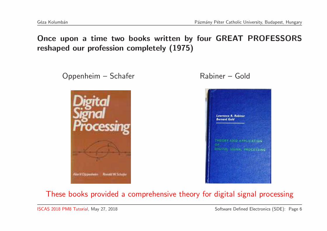
Once upon a time two books written by four GREAT PROFESSORSreshaped our profession completely (1975)
Oppenheim – Schafer Rabiner – Gold
These books provided a comprehensive theory for digital signal processing
ISCAS 2018 PM8 Tutorial, May 27, 2018 Software Defined Electronics (SDE): Page 6

Geza Kolumban Pazmany Peter Catholic University, Budapest, Hungary
Slogan: From education to research, from product development to mass production
Key issues to be discussed:
2 Theoretical background2.1 Concept of complex envelopes
2.2 Derivation of BaseBand (BB) equivalents
3 Key HW component: The universal RF hardware device(Transformation between the analog RF bandpass and digital low-pass BB domains)
4 Embedded operation of universal HW transformer
5 Applications of equivalent baseband information processing5.1 Computer simulations
5.2 Industrial applications
5.3 Application in scientific research
6 Conclusions and acknowledgements
ISCAS 2018 PM8 Tutorial, May 27, 2018 Software Defined Electronics (SDE): Page 7
Geza Kolumban Pazmany Peter Catholic University, Budapest, Hungary
Slogan: From education to research, from product development to mass production
Contents:
1 Motivation and a new way of teaching and researching ICT systems
2 Theoretical background2.1 Concept of complex envelopes
2.2 Derivation of BaseBand (BB) equivalents
3 Key HW component: The universal RF hardware device(Transformation between the analog RF bandpass and digital low-pass BB domains)
4 Embedded operation of universal HW transformer
5 Applications of equivalent baseband information processing5.1 Computer simulations
5.2 Industrial applications
5.3 Application in scientific research
6 Conclusions and acknowledgements
ISCAS 2018 PM8 Tutorial, May 27, 2018 Software Defined Electronics (SDE): Page 101
Geza Kolumban Pazmany Peter Catholic University, Budapest, Hungary
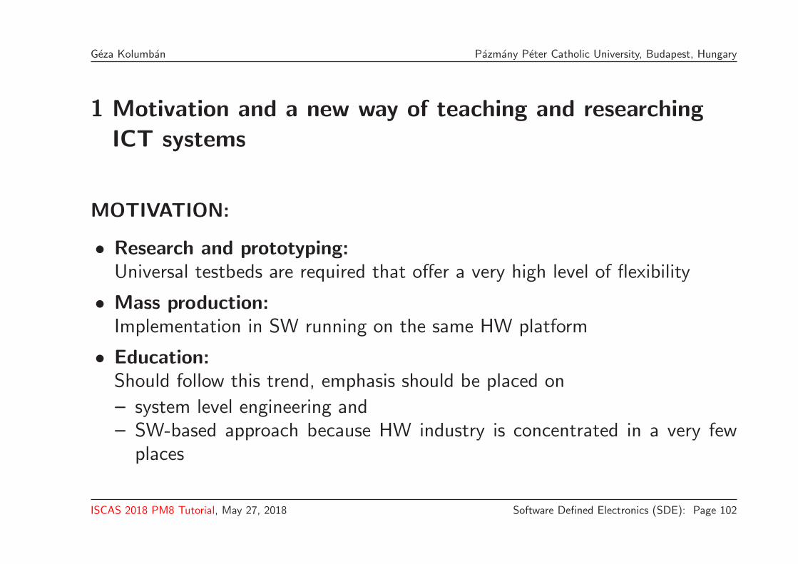
1 Motivation and a new way of teaching and researching
ICT systems
MOTIVATION:
• Research and prototyping:Universal testbeds are required that offer a very high level of flexibility
• Mass production:Implementation in SW running on the same HW platform
• Education:Should follow this trend, emphasis should be placed on
– system level engineering and– SW-based approach because HW industry is concentrated in a very few
places
ISCAS 2018 PM8 Tutorial, May 27, 2018 Software Defined Electronics (SDE): Page 102

Geza Kolumban Pazmany Peter Catholic University, Budapest, Hungary
TOPICS TO BE DISCUSSED:
1.1 Why SDE?
1.2 Example: Teaching waveform communications via hands-on examples
Classroom demonstrations with a laptop and two USRP units
Application of SDE concept in scientific research will be discussed later
ISCAS 2018 PM8 Tutorial, May 27, 2018 Software Defined Electronics (SDE): Page 103

Geza Kolumban Pazmany Peter Catholic University, Budapest, Hungary
1.1 Why SDE?
(Only the most important reasons)
• Today theory and practice are almost completely separated in teachingand researching ICT systems
• The time is never enough in education and research, we always have verylimited financial resources
• Multifunctionality can be implemented, an important issue in cognitive radioand adaptive systems
• Make changes easy: a very important requirement in research and prototyping
• Reduce the required time to market in industry
• Reconfiguration of already deployed systems can be performed
• · · ·
ISCAS 2018 PM8 Tutorial, May 27, 2018 Software Defined Electronics (SDE): Page 104

Geza Kolumban Pazmany Peter Catholic University, Budapest, Hungary
1.2 TEACHING WAVEFORM COMMUNICATIONS VIA
HANDS-ON-EXAMPLES
Three levels:
(a) Simulation at system level to support the theoretical discussions– Simulation of a BPSK system
– Simulation of a M-ary QAM system
(b) Study of a working radio system and measurement equipment– FM radio receiver with a built-in spectrum analyzer
– RF spectrum monitoring
(c) Study, implementation and testing of a complete radio link– M-ary FSK transmitter
– M-ary FSK receiver
– M-ary FSK radio link
SDE implementations used in the demonstrations have been developed and/or modified by me,
Tamas Krebesz (my PhD student) and National Instruments
ISCAS 2018 PM8 Tutorial, May 27, 2018 Software Defined Electronics (SDE): Page 105

Geza Kolumban Pazmany Peter Catholic University, Budapest, Hungary
Simulation of a BPSK system
(Only system level simulation, not an implementation)
From left to right, upper
row
• Tx output spectrumin RF frequency do-
main
• Noisy received signalin AWGN channel
• Received signal intime domain
From left to right, lower
row
• Noisy received signalat the output of Rx
channel filter
• Eye diagram
• Constellation dia-
gram
ISCAS 2018 PM8 Tutorial, May 27, 2018 Software Defined Electronics (SDE): Page 106

Geza Kolumban Pazmany Peter Catholic University, Budapest, Hungary
Simulation of an M-ary QAM system
(Only simulation. For explanations refer to the labels on the Front Panel)
ISCAS 2018 PM8 Tutorial, May 27, 2018 Software Defined Electronics (SDE): Page 107

Geza Kolumban Pazmany Peter Catholic University, Budapest, Hungary
Insight into the SW side of equivalent BaseBand (BB) implementation
Part of the block diagramof M-ary QAM simulator
where in the complex waveform
• t0 is the start time of waveform (timestamp)
• dt is the time interval elapsed between two consecutive data points, i.e., sampling
time
• data values of waveform, i.e., the real and imaginary parts of complex envelope
Theory of complex envelopes will be discussed in the next section
ISCAS 2018 PM8 Tutorial, May 27, 2018 Software Defined Electronics (SDE): Page 108

Geza Kolumban Pazmany Peter Catholic University, Budapest, Hungary
FM radio receiver with a built-in spectrum analyzer
(Note the dual functionality: A working FM receiver and a spectrum analyzer)
ISCAS 2018 PM8 Tutorial, May 27, 2018 Software Defined Electronics (SDE): Page 109

Geza Kolumban Pazmany Peter Catholic University, Budapest, Hungary
RF spectrum monitoring
(A working implementation where a USRP unit is used to extract the complex envelope)
• Real (I) and imaginary
(I) components of com-
plex envelope are shown
in white and red, re-
spectively
• Note, the duration of
windowing can be set
by the number of Sam-
ples/Frame
• Red line in the Inten-
sity Chart gives the time
instant where the BB
Spectrum of Received
Signal is plotted
ISCAS 2018 PM8 Tutorial, May 27, 2018 Software Defined Electronics (SDE): Page 110

Geza Kolumban Pazmany Peter Catholic University, Budapest, Hungary
A working 4-FSK transmitter with Gaussian Tx filter
ISCAS 2018 PM8 Tutorial, May 27, 2018 Software Defined Electronics (SDE): Page 111

Geza Kolumban Pazmany Peter Catholic University, Budapest, Hungary
A working 4-FSK receiver
ISCAS 2018 PM8 Tutorial, May 27, 2018 Software Defined Electronics (SDE): Page 112

Geza Kolumban Pazmany Peter Catholic University, Budapest, Hungary
Contents:
1 Motivation and a new way of teaching and researching ICT systems
2 Theoretical background2.1 Concept of complex envelopes
2.2 Derivation of BaseBand (BB) equivalents
3 Key HW component: The universal RF hardware device(Transformation between the analog RF bandpass and digital low-pass BB domains)
4 Embedded operation of universal HW transformer
5 Applications of equivalent baseband information processing5.1 Computer simulations
5.2 Industrial applications
5.3 Application in scientific research
6 Conclusions and acknowledgements
ISCAS 2018 PM8 Tutorial, May 27, 2018 Software Defined Electronics (SDE): Page 201

Geza Kolumban Pazmany Peter Catholic University, Budapest, Hungary
2 Theoretical background (Part 1)
2.1 Concept of complex envelopes
Goals of equivalent baseband transformation:
• Reduce sampling frequency to its theoretically attainable minimum value
IN SUCH A WAY THAT
• preserve all information available in the original signal without any distortion
• Substitute high-frequency analog signal processing with low-frequency digital one in baseband
Properties of baseband equivalents:
• Each bandpass signal (either deterministic or random) and each bandpass system can be
fully represented by its complex envelope and its complex impulse response, respectively, in
baseband
• RF bandpass analog signal processing can be done in the BaseBand (BB) using low-frequency
equivalent baseband circuits
• RF bandpass analog signals can be fully recovered from the complex envelopes
ISCAS 2018 PM8 Tutorial, May 27, 2018 Software Defined Electronics (SDE): Page 202
Geza Kolumban Pazmany Peter Catholic University, Budapest, Hungary
Elements of system level analysis: • Deterministic signals
• Linear Time Invariant (LTI) blocks
• Random processes
TOPICS TO BE DISCUSSED:
2.1.1 Baseband representation of bandpass signals
2.1.2 Properties of complex envelopes
2.1.3 Transformation between the RF bandpass and and baseband domains
2.1.4 Description of modulations
2.1.5 BB equivalent of Linear Time Invariant (LTI) systems
2.1.6 Baseband representation of bandpass random processes
2.1.7 Block diagram of equivalent BB implementation
ISCAS 2018 PM8 Tutorial, May 27, 2018 Software Defined Electronics (SDE): Page 203

Geza Kolumban Pazmany Peter Catholic University, Budapest, Hungary
To get the lowest sampling rate, RF bandpass signal to be processed has tobe decomposed into product of a complex envelope and a carrier exp(jωct)
x(t) = ℜ [x(t) exp(jωct)]
Method: Steps of derivation of complex envelopes
1. RF bandpass signal
jX(f
)j
jX(f)j
f
�f
f
| {z }
2B
| {z }
2B
Note, sampling rate is
determined by (fc + B)
⇒
2. Pre-envelope
jX
+
(f)j
f
�f
f
2jX(f
)j
| {z }
2B
⇒
3. Complex envelope
f
|X(f)|
2|X(fc)|
fc−fc
︸︷︷︸B
Goal achieved: sampling
rate is determined by B
Note: To perform the transformation a one-sided spectrum has to be generated first
ISCAS 2018 PM8 Tutorial, May 27, 2018 Software Defined Electronics (SDE): Page 204

Geza Kolumban Pazmany Peter Catholic University, Budapest, Hungary
HILBERT TRANSFORM:
The tool used to form a one-sided spectrum
Consider a bandpass signal x(t) with its Fourier transform X(f). The Hilberttransform of x(t) is defined by
x(t) =1
π
∫ ∞
−∞
x(τ)
t − τdτ
Hilbert transform may be rewritten as a convolution
x(t) ⋆ h(t) =
∫ ∞
−∞
x(τ)h(t − τ)dτ =
∫ ∞
−∞
x(τ)1
π(t − τ)dτ = x(t) ⋆
1
πt
and the Hilbert transform becomes a product in the frequency domain
X(f) = −jsgn(f)X(f)
ISCAS 2018 PM8 Tutorial, May 27, 2018 Software Defined Electronics (SDE): Page 205

Geza Kolumban Pazmany Peter Catholic University, Budapest, Hungary
2.1.1 BASEBAND REPRESENTATION OF BANDPASS SIGNALS
Consider a bandpass signal x(t) with a total bandwidth of 2B centered abouta center frequency fc and with its Fourier transform X(f) =
∫ ∞
−∞x(t)e−j2πftdt
Pre-envelope
The pre-envelope, also called analytic signal, is defined by
x+(t) = x(t) + jx(t)
Exploiting Hilbert transform, the spectrum of pre-envelope is obtained as
X+(f) = X(f) + j[−jsgn(f)X(f)] = X(f)[1 + sgn(f)] =
2X(f), f > 0
X(f), f = 0
0, f < 0
Note: Goal achieved, the pre-envelope has one-sided spectrum
ISCAS 2018 PM8 Tutorial, May 27, 2018 Software Defined Electronics (SDE): Page 206

Geza Kolumban Pazmany Peter Catholic University, Budapest, Hungary
COMPLEX ENVELOPE: Shifting the spectrum of pre-envelope to zero
1. RF bandpass signal
jX(f
)j
jX(f)j
f
�f
f
| {z }
2B
| {z }
2B
fsampling > 2(fc + B)
⇒
2. Pre-envelope
jX
+
(f)j
f
�f
f
2jX(f
)j
| {z }
2B
⇒
3. Complex envelope
f
|X(f)|
2|X(fc)|
fc−fc
︸︷︷︸B
fsampling > 2B
Price to be paid:
Complex envelope to be processed is a complex-valued function of time
x(t) = xI(t) + jxQ(t) = x+(t) exp(−jωct)
where xI(t) and xQ(t) are the in-phase and quadrature components of x(t), respectively
ISCAS 2018 PM8 Tutorial, May 27, 2018 Software Defined Electronics (SDE): Page 207

Geza Kolumban Pazmany Peter Catholic University, Budapest, Hungary
2.1.2 PROPERTIES OF COMPLEX ENVELOPE
Recall, definition of complex envelope: x(t) = ℜ [x(t) exp(jωct)]
Canonical form of RF bandpass signal: x(t) = xI(t) cos(ωt) − xQ(t) sin(ωt)
Properties:
In time domain:
A slowly-varyingcomplex-valued signal
x(t) = xI(t) + jxQ(t)
In frequency domain: A low-pass signal
f
|X(f)|
2|X(fc)|
fc−fc
︸︷︷︸B
Note: The only information which is not included in BB equivalent is fc
ISCAS 2018 PM8 Tutorial, May 27, 2018 Software Defined Electronics (SDE): Page 208

Geza Kolumban Pazmany Peter Catholic University, Budapest, Hungary
2.1.3 TRANSFORMATION BETWEEN RF BANDPASS AND BASE-BAND DOMAINS
Generation of in-phase and quadrature components of complex envelope
-2
2
x
Q
(t)
x
I
(t)
sin(!
t)
os(!
t)
x(t)
Processing: • Processing of complex-valued signal is not a problem in SW implementations
because LabVIEW and MATLAB use complex data-flows and arrays, respec-
tively
• In circuit-based analog signal processing two arms have to be used where
frequency responses of I/Q arms have to be tightly matched. Even a small
mismatch error makes the implementation impossible
ISCAS 2018 PM8 Tutorial, May 27, 2018 Software Defined Electronics (SDE): Page 209

Geza Kolumban Pazmany Peter Catholic University, Budapest, Hungary
Reconstruction of a bandpass signal from the I/Q components
Derivation of the canonical form of an RF bandpass signal:
x(t) = ℜ [x(t) exp(jωct)] = xI(t) cos(ωct) − xQ(t) sin(ωct)
x(t)
�+
os(!
t)
sin(!
t)
x
Q
(t)
x
I
(t)
Note: • Except the carrier frequency ωc, the complex envelope carries all information
• RF bandpass signal may be reconstructed from its I/Q components by means of
a quadrature mixer, a standard building block of each IC technology
ISCAS 2018 PM8 Tutorial, May 27, 2018 Software Defined Electronics (SDE): Page 210

Geza Kolumban Pazmany Peter Catholic University, Budapest, Hungary
2.1.4 DESCRIPTION OF MODULATIONS
(Envelope and phase of a bandpass signal)
Complex envelope: x(t) = xI(t) + jxQ(t) = a(t) exp[jφ(t)]
RF bandpass signal:
x(t) = ℜ [x(t) exp(jωct)] = ℜ [a(t) exp (j[ωCt + φ(t)])] = a(t) cos [ωCt + φ(t)]
Envelope of a bandpass signal gives its amplitude modulation (AM)
a(t) = |x(t)| =√
x2I(t) + x2
Q(t)
Phase of a bandpass signal gives its angle modulation (PM and FM)
φ(t) = arctan
[xQ(t)
xI(t)
]= ℑm(ln[x(t)])
ISCAS 2018 PM8 Tutorial, May 27, 2018 Software Defined Electronics (SDE): Page 211
Geza Kolumban Pazmany Peter Catholic University, Budapest, Hungary
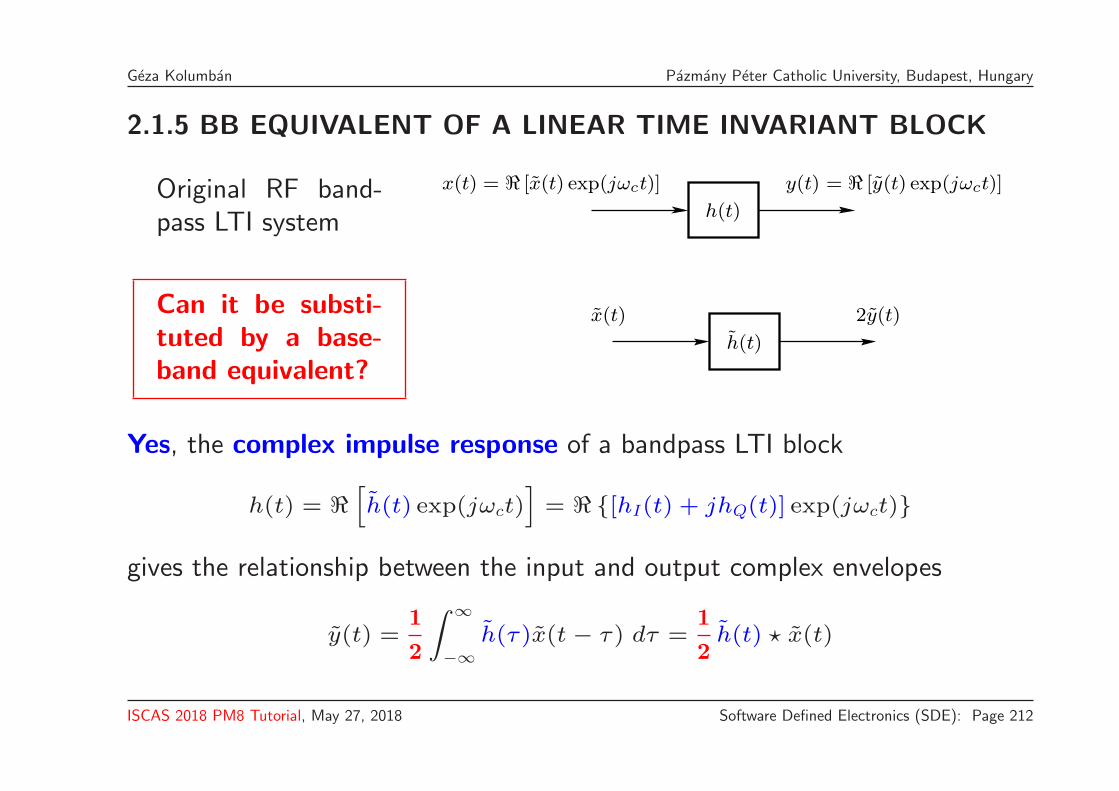
2.1.5 BB EQUIVALENT OF A LINEAR TIME INVARIANT BLOCK
Original RF band-pass LTI system
h(t)
x(t) = ℜ [x(t) exp(jωct)] y(t) = ℜ [y(t) exp(jωct)]
Can it be substi-tuted by a base-band equivalent?
h(t)
x(t) 2y(t)
Yes, the complex impulse response of a bandpass LTI block
h(t) = ℜ[h(t) exp(jωct)
]= ℜ{[hI(t) + jhQ(t)] exp(jωct)}
gives the relationship between the input and output complex envelopes
y(t) =1
2
∫ ∞
−∞
h(τ)x(t − τ) dτ =1
2h(t) ⋆ x(t)
ISCAS 2018 PM8 Tutorial, May 27, 2018 Software Defined Electronics (SDE): Page 212

Geza Kolumban Pazmany Peter Catholic University, Budapest, Hungary
Input-output relationship
y(t) =1
2
∫ ∞
−∞
h(τ)x(t−τ) dτ =1
2h(t)⋆x(t) =
1
2[hI(t) + jhQ(t)]⋆[xI(t) + jxQ(t)]
Note: Two complex quantities has to be convolved
hQ(t)
hI(t)
hQ(t)
hI(t)
xI(t)
xQ(t)
2yI(t)
2yQ(t)
The upper and lower arms are referred to as I− and Q−arms, respectively
ISCAS 2018 PM8 Tutorial, May 27, 2018 Software Defined Electronics (SDE): Page 213

Geza Kolumban Pazmany Peter Catholic University, Budapest, Hungary
2.1.6 BB REPRESENTATION OF RANDOM PROCESSES
Recall, both noise and interference are modeled as random processes
Mathematical model of a signal corrupted by noise or interference
White Gaussian noise
r(t)
Observable signalcorrupted by noise or interference
+
+
y(t)
Noise-free signalto be received or analyzed
w(t)
n(t)
RF bandpass random process
RF bandpass filter
2Bnoise
where 2Bnoise is greater or much greater than the RF bandwidth of y(t)
ISCAS 2018 PM8 Tutorial, May 27, 2018 Software Defined Electronics (SDE): Page 214

Geza Kolumban Pazmany Peter Catholic University, Budapest, Hungary
Properties of random process n(t) considered here
• Gaussian random process with zero mean
• n(t) is a bandpass process, its spectrum has a bandwidth of 2B centeredabout the center frequency ±fC
• Power Spectral Density (psd) SN(f) of n(t) is locally symmetric about thecenter frequencies ±fC
Let Rnn(τ) denote the autocorrelation function of RF bandpass noise n(t) tobe modeled
ISCAS 2018 PM8 Tutorial, May 27, 2018 Software Defined Electronics (SDE): Page 215

Geza Kolumban Pazmany Peter Catholic University, Budapest, Hungary
Representation of an RF bandpass random process in baseband
Bandpass random process n(t) can also be represented by its complex envelope
n(t) = ℜ [n(t) exp(jωCt)] = ℜ{[nI(t) + jnQ(t)] exp(jωCt)}
Recall, Power Spectral Density (psd) is used in frequency domain to characterize a randomprocess. Recall, psd of a random process is the Fourier transform of its autocorrelation function
• Let Rnn(τ) denote the autocorrelation function of n(t)
• Let RnInI(τ) and RnQnQ
(τ) denote the autocorrelation function of nI(t)and nQ(t), respectively
Relationship between the autocorrelation function of the RF bandpass randomprocess n(t) and that of the I/Q components of its complex envelope n(t)
Rnn(τ) = RnInI(τ) cos(ωCτ) = RnQnQ
(τ) cos(ωCτ) where RnInI(τ) = RnQnQ
(τ)
ISCAS 2018 PM8 Tutorial, May 27, 2018 Software Defined Electronics (SDE): Page 216

Geza Kolumban Pazmany Peter Catholic University, Budapest, Hungary
Properties of quadrature components of equivalent baseband noise
1. If n(t) is a Gaussian process and is stationary in wide-sense then both nI(t)and nQ(t) are jointly Gaussian and jointly stationary in wide-sense
2. Since n(t) has zero mean, both nI(t) and nQ(t) have zero mean values
3. The correlation functions of nI(t) and nQ(t) satisfy the following equations
RnInI(τ) = nI(t)nI(t + τ) = nQ(t)nQ(t + τ) = RnQnQ
(τ)
RnInQ(τ) = nI(t)nQ(t + τ) = 0 = −nQ(t)nI(t + τ) = RnQnI
(τ)
where overbar symbolizes time-averaging
Note: • first equation shows that the autocorrelation functions of nI(t) and nQ(t) areequal to each other
• second one means that nI(t) and nQ(t) are independent, i.e., orthogonal.
Be careful, two different seeds have to be used in computer simulation!!!
ISCAS 2018 PM8 Tutorial, May 27, 2018 Software Defined Electronics (SDE): Page 217

Geza Kolumban Pazmany Peter Catholic University, Budapest, Hungary
Properties of quadrature components of equivalent baseband noise
(Continuation from the previous page)
4. Relationship between the autocorrelation functions gives the relationshipbetween the power spectral densities measured in the RF and BB domains
Rn(τ) = RnI(τ) cos(ωCτ) = RnQ
(τ) cos(ωCτ) where RnI(τ) = RnQ
(τ)
5. Both the in-phase and quadrature components have the same power spectraldensity which is related to the power spectral density SN(f) of n(t) as
SNI(f) = SNQ
(f) =
{SN(f − fC) + SN(f + fC), −Brand ≤ f ≤ Brand
0, elsewhere
where SN(f) is zero outside of fC − Brand ≤ |f | ≤ fC + Brand and fC > Brand
ISCAS 2018 PM8 Tutorial, May 27, 2018 Software Defined Electronics (SDE): Page 218
Geza Kolumban Pazmany Peter Catholic University, Budapest, Hungary
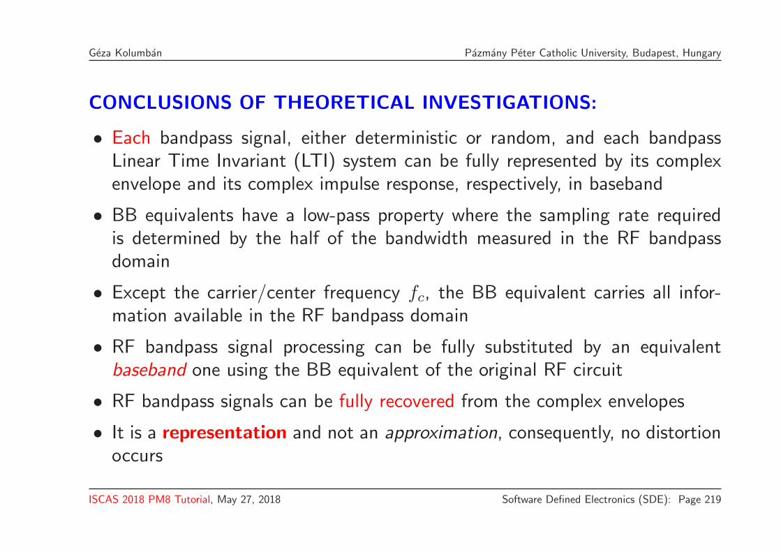
CONCLUSIONS OF THEORETICAL INVESTIGATIONS:
• Each bandpass signal, either deterministic or random, and each bandpassLinear Time Invariant (LTI) system can be fully represented by its complexenvelope and its complex impulse response, respectively, in baseband
• BB equivalents have a low-pass property where the sampling rate requiredis determined by the half of the bandwidth measured in the RF bandpassdomain
• Except the carrier/center frequency fc, the BB equivalent carries all infor-mation available in the RF bandpass domain
• RF bandpass signal processing can be fully substituted by an equivalentbaseband one using the BB equivalent of the original RF circuit
• RF bandpass signals can be fully recovered from the complex envelopes
• It is a representation and not an approximation, consequently, no distortionoccurs
ISCAS 2018 PM8 Tutorial, May 27, 2018 Software Defined Electronics (SDE): Page 219

Geza Kolumban Pazmany Peter Catholic University, Budapest, Hungary
Rule of thumb: Every RF bandpass property becomes low-pass in base-band
f
−fc fc
2B 2B
0
f
fc−fc B
0
N02
|X(fc)|, |H(fc)|,
|X(f)|
|H(f)|
|SN (f)|
|X(f)|
2|X(fc)|,
SNI(f)= SNQ(f)
|H(f)|
2|H(fc)|, N0
ISCAS 2018 PM8 Tutorial, May 27, 2018 Software Defined Electronics (SDE): Page 220

Geza Kolumban Pazmany Peter Catholic University, Budapest, Hungary
RF bandpass domain and its low-pass BB equivalents
RF bandpass domain BB low-pass domain
Deterministic signal x(t) x(t)
LTI two-port h(t) h(t)
LTI output y(t) y(t)
=∫ ∞
−∞h(τ)x(t − τ) dτ = 1
2
∫ ∞
−∞h(τ)x(t − τ) dτ
Random process n(t) n(t)
Only price to be paid: Complex-valued signals and functions have to be processed
ISCAS 2018 PM8 Tutorial, May 27, 2018 Software Defined Electronics (SDE): Page 221

Geza Kolumban Pazmany Peter Catholic University, Budapest, Hungary
2.1.7 BLOCK DIAGRAM OF EQUIVALENT BB IMPLEMENTATION
EquivalentBB signalprocessing
BaseBand (BB)
BB to RFinverse
transformation
RF domain
RF to BBtransformation
RF domain
Signal analyzer Signal generator
Universal RFHW device
Implementation in SW Universal RFHW device
Demodulator or Modulator or
ADC DAC
I QQI
y(t)
xI [n]
xQ[n]
yI [n]
yQ[n]
x(t)
Remark: Transformation between RF and BB domains is performed by theuniversal RF HW device (discussed in the next section)
ISCAS 2018 PM8 Tutorial, May 27, 2018 Software Defined Electronics (SDE): Page 222

Geza Kolumban Pazmany Peter Catholic University, Budapest, Hungary
2 Theoretical background (Part 2)
2.2 Derivation of BB equivalents
Key issue: How to derive the baseband equivalents?
TOPICS TO BE DISCUSSED:
• Two approaches available for the derivation of BB equivalents
• The engineering approach
• Many examples for the derivation
ISCAS 2018 PM8 Tutorial, May 27, 2018 Software Defined Electronics (SDE): Page 223

Geza Kolumban Pazmany Peter Catholic University, Budapest, Hungary
TWO APPROACHES AVAILABLE FOR THE DERIVATION OF BBEQUIVALENTS
(i) Direct use of mathematical algorithms elaborated in signal processing
• Signal processing consider the topic as a mathematical problem
• Implementation issues are not considered
• Well-known, already proven solutions cannot be re-used
One example: H. Meyr et. al., “Digital Communication Receivers, Synchronization, Channel
Estimation, and Signal Processing ,” Wiley, 1997.
(ii) Concept elaborated in Software Defined Electronics (SDE)
• A step-by-step approach (proposed here) has been elaborated for the deriva-tion of BB equivalents
• Transformation of the already known and proved HW solutions into SW
• Exploit the idea of HW-SW co-design
• An engineering-based approach
ISCAS 2018 PM8 Tutorial, May 27, 2018 Software Defined Electronics (SDE): Page 224

Geza Kolumban Pazmany Peter Catholic University, Budapest, Hungary
Main features of the engineering-based SDE approach discussed here:
• Starts from the already known RF bandpass solution
• A step-by-step systematic approach is provided for the transformation
• The already known, used and proven solutions can be re-used
• Not a pure mathematical but an engineering-based approach
• A systematic use of the theorems of analog and digital signal processing
Most important abbreviations and notations:
BB baseband
BP bandpass
Rx/Tx receiver/transmitter
ZoH zero-order hold
xI(t) in-phase (real) part of complex envelope x(t)
xQ(t) quadrature (imaginary) part of complex envelope x(t)
ISCAS 2018 PM8 Tutorial, May 27, 2018 Software Defined Electronics (SDE): Page 225

Geza Kolumban Pazmany Peter Catholic University, Budapest, Hungary
PROBLEMS SOLVED HERE:
• BB equivalent of an analog FM modulator
• BB equivalent of a QPSK modulator with ZoH pulse shaping
• BB equivalent of a generic QPSK/O-QPSK modulator
• BB equivalent of an AWGN radio channel
• BB equivalent of a two-ray multipath radio channel
• Cascading BB equivalents
• Cancelling RF impairment in baseband
• Implementation and testing of a complete half-sine O-QPSK radio link
We will go from the simplest case to the most complex one
ISCAS 2018 PM8 Tutorial, May 27, 2018 Software Defined Electronics (SDE): Page 226

Geza Kolumban Pazmany Peter Catholic University, Budapest, Hungary
One remark: To get compact equations, a low-pass filtering function is definedhere to express the effect of ideal low-pass filtering
Low-pass filtering is veryfrequently used in SDE.For example, the transfor-mation from RF domain toBB is
2
-2 xQ(t)
x(t) cos(ωct)
sin(ωct)
xI(t)
hLP (t)
xLPin (t) xLP
out(t)
where the impulse response of ideal low-pass filter is
hLP (t) = 2B sinc(Bt) = 2Bsin(2πBt)
2πBt
By definition, function LP(·) of ideal low-pass filtering is
xLPout(t) = hLP (t) ∗ x
LPin (t) =
∫ ∞
−∞
2Bsin[2πB(t − τ)]
2πB(t − τ)xLPin (τ) dτ ≡ LP
[xLPin (t)
]
ISCAS 2018 PM8 Tutorial, May 27, 2018 Software Defined Electronics (SDE): Page 227

Geza Kolumban Pazmany Peter Catholic University, Budapest, Hungary
EXTRACTION OF COMPLEX ENVELOPE
Definition of complex envelope
x(t) = ℜ [x(t) exp(jωct)] = ℜ ([xI(t) + jxQ(t)] [cos(ωct) + j sin(ωct)])
where x(t) denotes the RF bandpass signal
From the equation above we get the RF bandpass signal in canonical form
x(t) = xI(t) cos(ωct) − xQ(t) sin(ωct)
Let us multiply both the LHS and RHS by cos(ωct)
x(t) cos(ωct) = xI(t) cos2(ωct) − xQ(t) sin(ωct) cos(ωct)
Exploiting the well-known “product-to-sum” trigonometric identities we get
x(t) cos(ωct) =xI(t)
2[1 + cos(2ωct)] −
xQ(t)
2sin(2ωct)
Let the spectra of 2nd & 3rd components on the RHS be evaluated by the modulation theorem
ISCAS 2018 PM8 Tutorial, May 27, 2018 Software Defined Electronics (SDE): Page 228

Geza Kolumban Pazmany Peter Catholic University, Budapest, Hungary
Modulation theorem:
Gives the spectrum of a low-pass signal multiplied by a carrier in the time-domain
Spectrum of xI(t)
Spectrum of [xI(t) cos(2ωCt)]
2fC−2fC 0
f
f
1
12
0
ISCAS 2018 PM8 Tutorial, May 27, 2018 Software Defined Electronics (SDE): Page 229

Geza Kolumban Pazmany Peter Catholic University, Budapest, Hungary
Signal before low-pass filtering
x(t) cos(ωct) =xI(t)
2[1 + cos(2ωct)] −
xQ(t)
2sin(2ωct)
Let the low-pass filtering be applied to both sides
LP {x(t) cos(ωct)} = LP
{xI(t)
2[1 + cos(2ωct)] −
xQ(t)
2sin(2ωct)
}=
xI(t)
2
Solution: Extraction of in-phase and quadrature components:
-2
2
x
Q
(t)
x
I
(t)
sin(!
t)
os(!
t)
x(t)
ISCAS 2018 PM8 Tutorial, May 27, 2018 Software Defined Electronics (SDE): Page 230

Geza Kolumban Pazmany Peter Catholic University, Budapest, Hungary
RECONSTRUCTION OF RF BANDPASS SIGNAL
Recall, definition of complex envelope
x(t) = ℜ [x(t) exp(jωct)] = ℜ ([xI(t) + jxQ(t)] [cos(ωct) + j sin(ωct)])
From the equation above we get the RF bandpass signal in canonical form
x(t) = xI(t) cos(ωct) − xQ(t) sin(ωct)
Solution: Reconstruction of RF bandpass signal from the I/Q componentsx(t)
�+
os(!
t)
sin(!
t)
x
Q
(t)
x
I
(t)
ISCAS 2018 PM8 Tutorial, May 27, 2018 Software Defined Electronics (SDE): Page 231

Geza Kolumban Pazmany Peter Catholic University, Budapest, Hungary
EXAMPLE 1
Objective: Derivation of low-pass BB equivalent of an analog FM modulator
Block diagram:
FM MOD sFMRF (t)m(t)
RF bandpass signal
sFMRF (t) = AC cos
[ωCt + 2πkf
∫ t
0
m(τ)dτ
]
ISCAS 2018 PM8 Tutorial, May 27, 2018 Software Defined Electronics (SDE): Page 232

Geza Kolumban Pazmany Peter Catholic University, Budapest, Hungary
Derivation:
Extracting the complex envelope from the FM signal (bandpass RF signal)
cos(ωct)
-2
2
sFMRF
(t) = Ac cos[
ωct+ 2πkf∫ t0 m(τ)dτ
]
sin(ωct)
sFMI (t)
sFMQ
(t)
sMI (t)
sMQ
(t)
Output of the upper in-phase multiplier
sMI (t) = Ac cos
[ωct + 2πkf
∫ t
0
m(τ)dτ
]cosωct
Exploiting the “product-to-sum” trigonometric identity
sMI (t) =
Ac
2
(cos
[2πkf
∫ t
0
m(τ)dτ
]+ cos
[2ωct + 2πkf
∫ t
0
m(τ)dτ
])
ISCAS 2018 PM8 Tutorial, May 27, 2018 Software Defined Electronics (SDE): Page 233

Geza Kolumban Pazmany Peter Catholic University, Budapest, Hungary
Ideal low-pass filter suppresses the sum frequency component
sFMI (t) = 2LP
{sMI (t)
}= Ac cos
[2πkf
∫ t
0
m(τ)dτ
]
Quadrature component is obtained in a similar manner
sFMQ (t) = Ac sin
[2πkf
∫ t
0
m(τ)dτ
]
Block diagram of BB equivalent can be depicted from these equations
ISCAS 2018 PM8 Tutorial, May 27, 2018 Software Defined Electronics (SDE): Page 234

Geza Kolumban Pazmany Peter Catholic University, Budapest, Hungary
Solution: BB equivalent of the analog FM modulator
Generation of complex envelope
AC sin(.)
sFMI (t)
m(t)
AC cos(.)
2πkft∫
0
. dτsFMQ (t)
BB implementation in SW
Reconstruction of RF bandpass
signal
x(t)
�+
os(!
t)
sin(!
t)
x
Q
(t)
x
I
(t)
Universal RF HW device
(transformer)
ISCAS 2018 PM8 Tutorial, May 27, 2018 Software Defined Electronics (SDE): Page 235
Geza Kolumban Pazmany Peter Catholic University, Budapest, Hungary
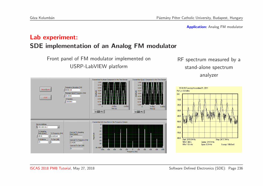
Application: Analog FM modulator
Lab experiment:
SDE implementation of an Analog FM modulator
Front panel of FM modulator implemented on
USRP-LabVIEW platform
RF spectrum measured by a
stand-alone spectrum
analyzer
ISCAS 2018 PM8 Tutorial, May 27, 2018 Software Defined Electronics (SDE): Page 236

Geza Kolumban Pazmany Peter Catholic University, Budapest, Hungary
EXAMPLE 2Objective: Derivation of BB equivalent of a QPSK modulator with ZoH pulse shaping filter
Recall: Definition of QPSK modulator with ZoH pulse shaping in telecommunications
s
m2
s
m1
++
s
m
(t)
g
1
(t)
g
2
(t)
g1(t)√
2/T cos(ωCt)
g2(t)√
2/T sin(ωCt)
# of symbols 4
sm
√Eb2√Eb2
· · ·
√Eb2
−
√Eb2
Reconstruction of RF bandpass signal
x(t)
�+
os(!
t)
sin(!
t)
x
Q
(t)
x
I
(t)
By inspection:
• Two ZoH circuits are needed to keep
xI(t) and xQ(t) constant for T
• sm1 ∼ xI(t) and sm2 ∼ xQ(t)
• Note the “-” sign
ISCAS 2018 PM8 Tutorial, May 27, 2018 Software Defined Electronics (SDE): Page 237

Geza Kolumban Pazmany Peter Catholic University, Budapest, Hungary
Solution: BB equivalent of the digital QPSK modulator
Generation of complex envelope
Pulse Shaping Filter
Pulse Shaping Filter
ZoH
ZoH
ConverterBit2symbol
±1
±1
−
√
EbT
sQPSKI
(t)
sQPSKQ
(t)
√
EbT
bi
BB implementation in SW
Reconstruction of RF bandpass
signal
x(t)
�+
os(!
t)
sin(!
t)
x
Q
(t)
x
I
(t)
Universal RF HW device
(transformer)
ISCAS 2018 PM8 Tutorial, May 27, 2018 Software Defined Electronics (SDE): Page 238

Geza Kolumban Pazmany Peter Catholic University, Budapest, Hungary
EXAMPLE 3
Objective: Derivation of low-pass equivalent of an Offset QPSK with half-sinepulse shaping (used by IEEE 802.15.5 “ZigBee,” 2.4 GHz)
Odd Even
p(t)
+
+
cos(ωct)
sin(ωct)
p(t)Delay
Tc
bi sO−QPSK(t)
±b0, · · ·
±b1, · · ·
where
p(t) =
sin
(π t
2Tc
), 0 ≤ t ≤ 2Tc
0, otherwisewhere Tc denotes the chip duration
ISCAS 2018 PM8 Tutorial, May 27, 2018 Software Defined Electronics (SDE): Page 239

Geza Kolumban Pazmany Peter Catholic University, Budapest, Hungary
Solution by inspection: BB equivalent of generic O-QPSK/QPSK modulator
Generation of complex envelope
Pulse Shaping Filter
Pulse Shaping Filter
Delay
ConverterBit2symbol
TS
2
-1
sO−QPSKI
(t)
sO−QPSKQ
(t)
bi
BB implementation in SW
Reconstruction of RF BP signal
x(t)
�+
os(!
t)
sin(!
t)
x
Q
(t)
x
I
(t)
Universal RF HW device
(transformer)
Remarks: • Impulse response of pulse shaping Tx filter and delay have to be set
• Constants fixing Eb are set in the “Bit2symbol Converter”
ISCAS 2018 PM8 Tutorial, May 27, 2018 Software Defined Electronics (SDE): Page 240
Geza Kolumban Pazmany Peter Catholic University, Budapest, Hungary
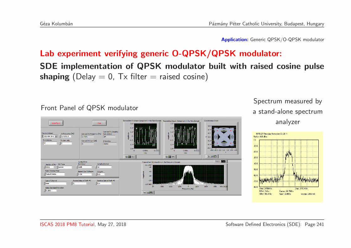
Application: Generic QPSK/O-QPSK modulator
Lab experiment verifying generic O-QPSK/QPSK modulator:
SDE implementation of QPSK modulator built with raised cosine pulseshaping (Delay = 0, Tx filter = raised cosine)
Front Panel of QPSK modulatorSpectrum measured by
a stand-alone spectrum
analyzer
ISCAS 2018 PM8 Tutorial, May 27, 2018 Software Defined Electronics (SDE): Page 241
Geza Kolumban Pazmany Peter Catholic University, Budapest, Hungary
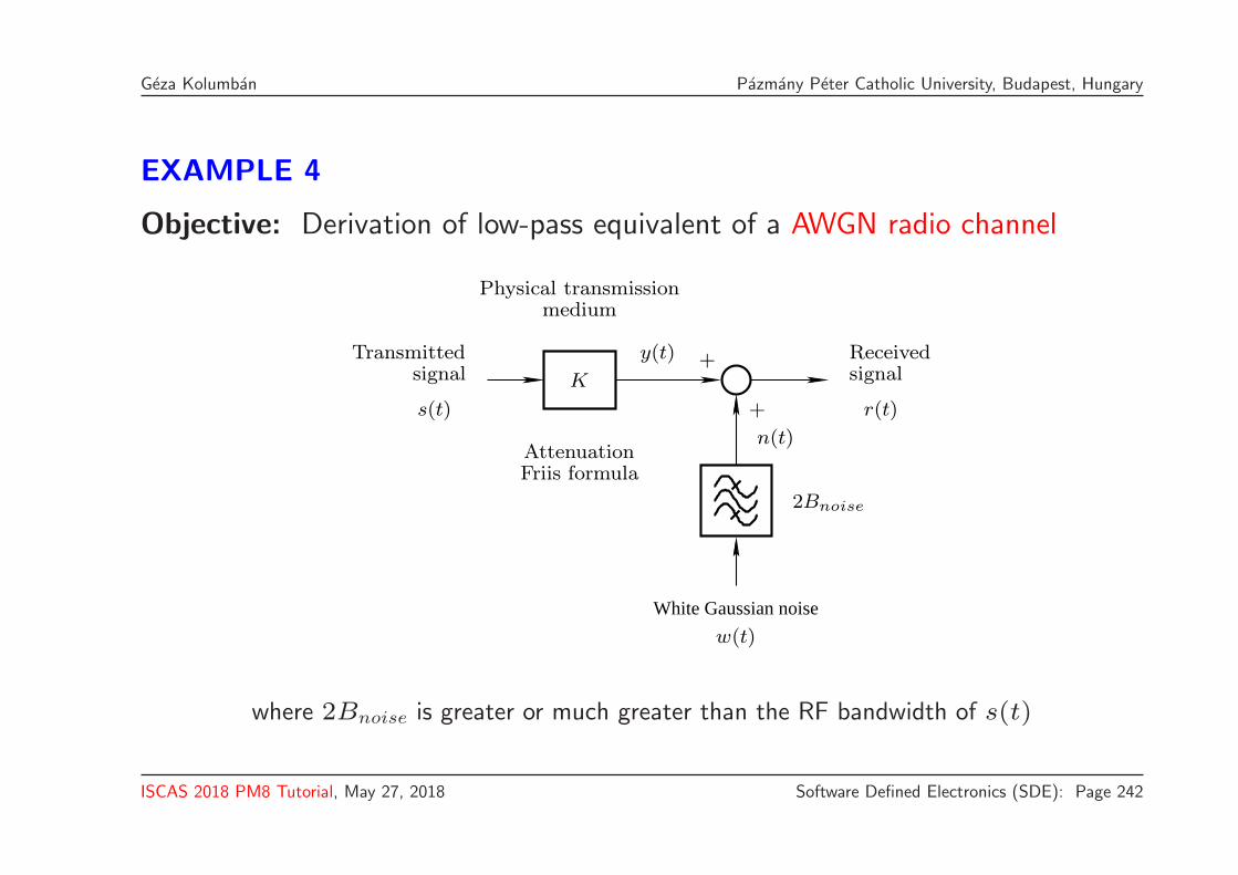
EXAMPLE 4
Objective: Derivation of low-pass equivalent of a AWGN radio channel
White Gaussian noise
signal
s(t)
Transmitted y(t)
+
+
n(t)
r(t)
ReceivedsignalK
AttenuationFriis formula
Physical transmissionmedium
w(t)
2Bnoise
where 2Bnoise is greater or much greater than the RF bandwidth of s(t)
ISCAS 2018 PM8 Tutorial, May 27, 2018 Software Defined Electronics (SDE): Page 242

Geza Kolumban Pazmany Peter Catholic University, Budapest, Hungary
Derivation
Step #1: Complete RF AWGN with the two transformations (BB=>RF & RF=>BB)
RF BP AWGN
+
+y(t)
w(t)
K
−
+
cos(ωct)
sin(ωct)
sI(t)
s(t)
sQ(t)
2Bnoise
-2
sin(ωct)
cos(ωct)
rI(t)
rQ(t)
2
n(t)
wB(t)
wG(t)
r(t)
Transformation by applying the rules of block diagram algebra
1. Move RF BP AWGN beyond the pickoff point marked by the red circle
2. Exchange the order of RF BP AWGN part moved beyond the pickoff point and the in-phasearm depicted in blue
ISCAS 2018 PM8 Tutorial, May 27, 2018 Software Defined Electronics (SDE): Page 243

Geza Kolumban Pazmany Peter Catholic University, Budapest, Hungary
Step #2: After applying the rules of block diagram algebra
cos(ωct)
sin(ωct)
−
+
cos(ωct)
sin(ωct)
sI(t)
2
s(t)
sQ(t)
LP1
LP1
−2K
2K
cos(ωct)
sin(ωct)
+
+
+
-2
+
LP2
n(t)w(t)
2Bnoise
yI(t)
yQ(t)
rQ(t)
rI(t)
nQ(t)
nI(t)
LP2
wG(t)
Note, the original path of
wB(t) has been substituted
by the green one wG(t)
Note: nI(t) and nQ(t) are the in-phase and quadrature components of complex envelope ofchannel noise n(t) that can be directly generated in baseband
ISCAS 2018 PM8 Tutorial, May 27, 2018 Software Defined Electronics (SDE): Page 244

Geza Kolumban Pazmany Peter Catholic University, Budapest, Hungary
Step #3: Eliminate RF bandpass signal s(t)
−
+
cos(ωct)
sin(ωct)
sI(t)+
yI(t)
rI(t)+
rQ(t)
nI(t)
nQ(t)
yQ(t)
+
+sQ(t)
cos(ωct)
sin(ωct)
−2K
2K
s(t)
Effect of sI(t) on yI(t)
y[sI ]
I (t) = LP[sI(t) cos
2(ωct)
]× 2K = 2K × LP
[sI(t)
1 + cos(2ωct)
2
]= K sI(t)
Effect of sQ(t) on yI(t) is zero because
y[sQ]
I (t) = LP [−sQ(t) sin(ωct) cos(ωct)]︸ ︷︷ ︸=0
×2K = 0
ISCAS 2018 PM8 Tutorial, May 27, 2018 Software Defined Electronics (SDE): Page 245

Geza Kolumban Pazmany Peter Catholic University, Budapest, Hungary
Step #4: Add channel noise
rI(t) = yI(t) + nI(t) = K sI(t) + nI(t)
In a similar manner rQ(t) can be expressed as
rQ(t) = K sQ(t) + nQ(t)
Solution: BB equivalent of the AWGN radio channel in the analog domain
K
K
sI(t)
sQ(t)
nI(t)
nQ(t)
yI(t)
yQ(t)
rQ(t)
rI(t)
ISCAS 2018 PM8 Tutorial, May 27, 2018 Software Defined Electronics (SDE): Page 246

Geza Kolumban Pazmany Peter Catholic University, Budapest, Hungary
SDE solution is obtained after digitizing the analog BB signals
Digitized BB equivalent of
AWGN channel
K
K
sI [n]
sQ[n]
yI [n]
rI [n]
nI [n]
yQ[n]
rQ[n]
nQ[n]
Two Gaussian Pseudo Ran-
dom Sequence Generators
(PRSGs) with different
seeds and prescribed vari-
ance have to be used
Spectrum in analog RF
domain
ωc
N0/2
ω−ωc
︸ ︷︷ ︸
ωs
︸ ︷︷ ︸
ωs
SN (ω)
Parameters:
2Bnoise = fS
var(nI[n]) = var(nQ[n])
= N0fS
Spectrum measured by a
stand-alone spectrum analyzer
Note the direct relationships among the parameters of RF bandpass and BB low-pass models!
ISCAS 2018 PM8 Tutorial, May 27, 2018 Software Defined Electronics (SDE): Page 247

Geza Kolumban Pazmany Peter Catholic University, Budapest, Hungary
Application: AWGN channel
Lab experiment: SDE implementation of an AWGN radio channel
Front panel of AWGN channel sounder implemented on
USRP-LabVIEW platform Measured RF spectrum of
generated channel noise
ISCAS 2018 PM8 Tutorial, May 27, 2018 Software Defined Electronics (SDE): Page 248

Geza Kolumban Pazmany Peter Catholic University, Budapest, Hungary
EXAMPLE 5
Objective: Derivation of low-pass equivalent of a two-ray multipath radiochannel
noiseWhite Gaussian
Transmittedsignal
s(t)
y(t)
mediumPhysical transmission
+
+
n(t)
r(t)
ReceiverinputEffect of
two-ray multipath
Note: • Because of cascading, only the multipath propagation has to be modeled here
• Other effect such as channel attenuation and noise have to be taken into account
by the AWGN channel model
ISCAS 2018 PM8 Tutorial, May 27, 2018 Software Defined Electronics (SDE): Page 249

Geza Kolumban Pazmany Peter Catholic University, Budapest, Hungary
Derivation
Step #1: Complete RF tapped delay line model with the two transformations
(BB=>RF & RF=>BB)
RF BP multipath channel
Gain
k2
Delay
T2
−
+
cos(ωct)
sin(ωct)
sI(t)
sQ(t)
+
+
s(t)r(t)
-2
2
sin(ωct)
cos(ωct)
rI(t)
rQ(t)
Direct relationships between rI(t)–rQ(t) and sI(t)–sQ(t) have to be found
1. Multipath channel is linear, consequently, superposition theorem can be applied
2. Apply the product-to-sum trigonometric identity and
3. Exploit the frequency shifting property of Fourier transform
ISCAS 2018 PM8 Tutorial, May 27, 2018 Software Defined Electronics (SDE): Page 250

Geza Kolumban Pazmany Peter Catholic University, Budapest, Hungary
Equations: Effect of sI(t) on rI(t)
r[sI ]
I (t) = 2 × LP [(sI(t) cos(ωct) + k2sI(t − T2) cos [ωc(t − T2)]) cos(ωct)]
= sI(t) + k2sI(t − T2) cos(ωcT2)
where LP [·], as before, describes the effect of low-pass filtering
Effect of sQ(t) on rI(t) is obtained in a similar manner
r[sQ]
I (t) = 2 × LP [(−sQ(t) sin(ωct) − k2sQ(t − T2) sin [ωc(t − T2)]) cos(ωct)]
= k2sQ(t − T2) sin(ωcT2)
By means of the superposition theorem, rI(t) is obtained as
rI(t) = sI(t) + k2sI(t − T2) cos(ωcT2) + k2sQ(t − T2) sin(ωcT2)
In a similar manner rQ(t) can be expressed as
rQ(t) = sQ(t) + k2sQ(t − T2) cos(ωcT2) − k2sI(t − T2) sin(ωcT2)
ISCAS 2018 PM8 Tutorial, May 27, 2018 Software Defined Electronics (SDE): Page 251

Geza Kolumban Pazmany Peter Catholic University, Budapest, Hungary
Step #2: To get a compact notation, equations given on the previous slide are rewritten as
[rI(t)
rQ(t)
]=
[sI(t)
sQ(t)
]+ k2
[cos(ωcT2) sin(ωcT2)
− sin(ωcT2) cos(ωcT2)
]
︸ ︷︷ ︸=D
[sI(t − T2)
sQ(t − T2)
]
Solution: BB equivalent of a two-ray noise-free multipath radio channel
Gain Delay
k2 T2
sI(t)
sQ(t)
Gain Delay
k2 T2
D
rI(t)
rQ(t)
ISCAS 2018 PM8 Tutorial, May 27, 2018 Software Defined Electronics (SDE): Page 252

Geza Kolumban Pazmany Peter Catholic University, Budapest, Hungary
EXAMPLE 6
Objective: Derivation of low-pass equivalent of two two-ports connected incascade in the RF domain
Cascade connection of Block A and Block B in the RF bandpass domain
hA(t) hB(t)x(t) y(t)
Step #1: Complete the two RF blocks with RF=>BB & BB=>RF transformations
-2
sin(ωct)
cos(ωct)
2
hA(t)−
+
cos(ωct) hB(t)−
+
cos(ωct)x(t)
AI(t)
AQ(t)
yI(t)
yQ(t)
BI (t)
BQ(t)
xI(t)
xQ(t)
sin(ωct)
-2
cos(ωct)
2
sin(ωct)sin(ωct)
y(t)
ISCAS 2018 PM8 Tutorial, May 27, 2018 Software Defined Electronics (SDE): Page 253

Geza Kolumban Pazmany Peter Catholic University, Budapest, Hungary
Step #2: Eliminate RF bandpass signals by exploiting superposition theorem
-2
sin(ωct)
cos(ωct)
2
hA(t)−
+
cos(ωct) hB(t)−
+
cos(ωct)x(t)
AI(t)
AQ(t)
yI(t)
yQ(t)
BI (t)
BQ(t)
xI(t)
xQ(t)
sin(ωct)
-2
cos(ωct)
2
sin(ωct)sin(ωct)
y(t)
Effects of AI(t) on BI(t)
B[AI ]
I (t) = LP[AI(t) cos
2(ωct)
]× 2 = 2 × LP
[AI(t)
1 + cos(2ωct)
2
]= AI(t)
Effect of AQ(t) on BI(t) is zero because
B[AQ]
I (t) = LP [−AQ(t) sin(ωct) cos(ωct)]︸ ︷︷ ︸=0
×2 = 0
ISCAS 2018 PM8 Tutorial, May 27, 2018 Software Defined Electronics (SDE): Page 254

Geza Kolumban Pazmany Peter Catholic University, Budapest, Hungary
Step #3: Good news — Cascading is preserved in BB!
hA(t)
xI(t)
xQ(t)
AQ(t) = BQ(t)
AI(t) = BI(t)
hB(t)
yI (t)
yQ(t)
Because cascading is preserved in BB
• block diagram of a BB equivalent will be identical with that of the RF blockdiagram
• library elements and libraries can be developed and used
ISCAS 2018 PM8 Tutorial, May 27, 2018 Software Defined Electronics (SDE): Page 255

Geza Kolumban Pazmany Peter Catholic University, Budapest, Hungary
Application of cascading (example #1)
Objective: Derivation of low-pass equivalent of the generation of noisy O-QPSK signal
Block diagram in the RF bandpass domain
Odd Even
p(t)
+
+
n(t)
r(t)cos(ωct)
sin(ωct)
p(t)Delay
Tc
bi
b1, · · ·
b0, · · ·
+
+
K
sO−QPSK(t)
where
p(t) =
sin
(π t
2Tc
), 0 ≤ t ≤ 2Tc
0, otherwise
ISCAS 2018 PM8 Tutorial, May 27, 2018 Software Defined Electronics (SDE): Page 256

Geza Kolumban Pazmany Peter Catholic University, Budapest, Hungary
As library blocks, BB equivalents of both O-QPSK modulator and AWGNchannel are available
Solution:
BB equivalent of the generation of noisy O-QPSK signal
bit2symbolConverter
Pulse Shaping Filter
Pulse Shaping Filter
DelayTS
2
bi
-1
yI(t)
rI(t)
yQ(t)
rQ(t)
nI(t)
nQ(t)
sO−QPSKI
(t)
sO−QPSKQ
(t)
K
K
ISCAS 2018 PM8 Tutorial, May 27, 2018 Software Defined Electronics (SDE): Page 257

Geza Kolumban Pazmany Peter Catholic University, Budapest, Hungary
Application: Half-sine O-QPSK modulator communicating over AWGN channel
Lab experiment:
SDE implementation of half-sine O-QPSK modulator with an AWGNchannel emulator using library blocks
Front Panel of SDE implementing both the
half-sine O-QPSK modulator and AWGN channel
Spectrum measured by
a stand-alone spectrum
analyzer
Note: • A Gaussian cloud appears around each message point
ISCAS 2018 PM8 Tutorial, May 27, 2018 Software Defined Electronics (SDE): Page 258

Geza Kolumban Pazmany Peter Catholic University, Budapest, Hungary
Application of cascading (example #2)
Objective: Derivation of low-pass equivalent of the O-QPSK modulator and a noisy
multipath channel
Recall, as library blocks, BB equivalents of O-QPSK modulator, multipath propagation and
channel noise are available
Solution: BB equivalent of O-QPSK modulator with noisy multipath channel
bit2symbolConverter
Pulse Shaping Filter
Pulse Shaping Filter
Delay
O−QPSK modulator Multipath propagation AWGN channel
TS
2
bi
Gain Delay
k2 T2
yI(t)
nI(t)
K rI(t)
rQ(t)
yQ(t)
nQ(t)
K
Gain Delay
k2 T2
D
sO−QPSKQ
(t)
sO−QPSKI
(t)
-1
ISCAS 2018 PM8 Tutorial, May 27, 2018 Software Defined Electronics (SDE): Page 259
Geza Kolumban Pazmany Peter Catholic University, Budapest, Hungary
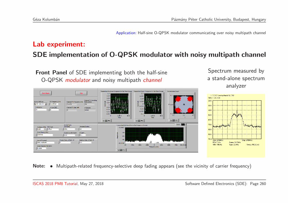
Application: Half-sine O-QPSK modulator communicating over noisy multipath channel
Lab experiment:
SDE implementation of O-QPSK modulator with noisy multipath channel
Front Panel of SDE implementing both the half-sine
O-QPSK modulator and noisy multipath channel
Spectrum measured by
a stand-alone spectrum
analyzer
Note: • Multipath-related frequency-selective deep fading appears (see the vicinity of carrier frequency)
ISCAS 2018 PM8 Tutorial, May 27, 2018 Software Defined Electronics (SDE): Page 260

Geza Kolumban Pazmany Peter Catholic University, Budapest, Hungary
EXAMPLE 7
Objective: Cancelling RF impairment in baseband
Problem: • Two stand-alone test beds (a 16-QAM Tx and a 16-QAM Rx) were implemented
• Frequency/phase error cancellation algorithms were not robust enough, synchro-
nization was frequently lost
• An external common reference signal was used to eliminate frequency error
• But a phase error introduced by the RF cables was still present and adjustable
microwave phase shifter was not available to cancel the phase error
Block diagram of test bed
External reference
External reference input
Phase shift
External reference input
USRP #1
Tx Rx
USRP #2sI(t)
sQ(t)
rI (t)
rQ(t)
φsignal fc
Question: How to cancel the RF phase error in baseband?
ISCAS 2018 PM8 Tutorial, May 27, 2018 Software Defined Electronics (SDE): Page 261
Geza Kolumban Pazmany Peter Catholic University, Budapest, Hungary
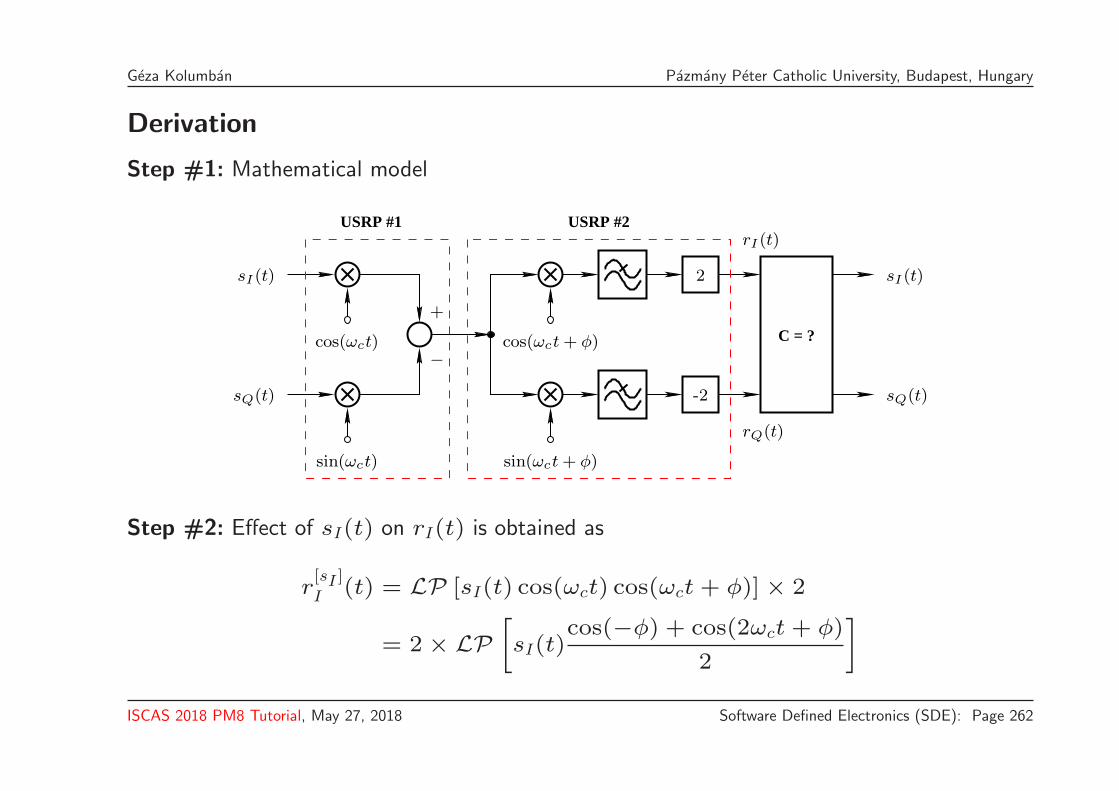
Derivation
Step #1: Mathematical model
C = ?
USRP #1 USRP #2
−
+
cos(ωct)
sin(ωct)
-2
2
cos(ωct+ φ)
sin(ωct+ φ)
sI(t)
sQ(t)
sI(t)
sQ(t)
rI(t)
rQ(t)
Step #2: Effect of sI(t) on rI(t) is obtained as
r[sI ]
I (t) = LP [sI(t) cos(ωct) cos(ωct + φ)] × 2
= 2 × LP
[sI(t)
cos(−φ) + cos(2ωct + φ)
2
]
ISCAS 2018 PM8 Tutorial, May 27, 2018 Software Defined Electronics (SDE): Page 262

Geza Kolumban Pazmany Peter Catholic University, Budapest, Hungary
Exploiting modulation theorem and considering the effect of low-pass filtering
r[sI ]
I (t) = sI(t) cos(φ)
The other components in rI(t) and rQ(t) are obtained in a similar manner
r[sQ]
I (t) = sQ(t) sin(φ), r[sI ]
Q (t) = −sI(t) sin(φ) and r[sQ]
Q (t) = sQ(t) cos(φ)
After applying the superposition theorem and using a compact notation we get
[rI(t)
rQ(t)
]=
[cos(φ) sin(φ)
− sin(φ) cos(φ)
]
︸ ︷︷ ︸=A
[sI(t)
sQ(t)
]
Note: Phase shift φ generates a cross-coupling between the in-phase and quadrature arms
ISCAS 2018 PM8 Tutorial, May 27, 2018 Software Defined Electronics (SDE): Page 263

Geza Kolumban Pazmany Peter Catholic University, Budapest, Hungary
Step #3: Compensation of RF phase shift in BB with a matrix C
C
[rI(t)
rQ(t)
]= CA︸︷︷︸
=I
[sI(t)
sQ(t)
]=
[sI(t)
sQ(t)
]
Solution: Cancellation of RF phase shift in BB
C = A−1 =
[cos(φ) − sin(φ)sin(φ) cos(φ)
]
ISCAS 2018 PM8 Tutorial, May 27, 2018 Software Defined Electronics (SDE): Page 264

Geza Kolumban Pazmany Peter Catholic University, Budapest, Hungary
Application: Phase error cancellation in baseband
Lab experiment:
SDE implementation of BB phase error cancellation
Note: Constellation diagram can be rotated by tuning the “Phase shift” knob
ISCAS 2018 PM8 Tutorial, May 27, 2018 Software Defined Electronics (SDE): Page 265

Geza Kolumban Pazmany Peter Catholic University, Budapest, Hungary
EXAMPLE 8
Objective: Implementation and testing a complete radio link
Parts of an RF radio link • TransmitterGeneric QPSK/O-QPSK modulator is available
• Radio channelAWGN, multipath and noisy multipath channelsare available
• Generic QPSK/O-QPSK receiverTo be implemented
ISCAS 2018 PM8 Tutorial, May 27, 2018 Software Defined Electronics (SDE): Page 266

Geza Kolumban Pazmany Peter Catholic University, Budapest, Hungary
Derivation of generic QPSK/O-QPSK demodulator
Generic QPSK/O-QPSK demodulator in the RF domain
Symbol−timing
Receive
Receive
Even OddCarrier
Offset delay
circuitDecision
circuitDecision
r(t)
sin(ωct)
cos(ωct)
RI (t)
RQ(t)
0
−
π2
TS
Threshold
Threshold
Threshold
In-phase channel
Quadrature channel
recovery
filter
filter
recovery
TS
2
bi
Recall, extraction of I/Q
components
-2
2
x
Q
(t)
x
I
(t)
sin(!
t)
os(!
t)
x(t)
BB equivalent of generic QPSK/O-QPSK demodulator is obtained by inspection
Symbol−timing symbol2bit
converter
Offset delay
1
2
circuitDecision
circuitDecision
RI(t)
RQ(t)
TS
−
1
2
rQ(t)
rI (t)
Threshold
Threshold
recovery
TS
2
bi
Note: • For QPSK, offset delay TS/2 has to be set to zero
ISCAS 2018 PM8 Tutorial, May 27, 2018 Software Defined Electronics (SDE): Page 267

Geza Kolumban Pazmany Peter Catholic University, Budapest, Hungary
Test bed developed to implement a complete digital radio link
USRP
# 2
Configuration # 2Receiver
EthernetGigabit
TransmitterConfiguration # 1
EthernetGigabit
USRP
# 1
USB Interface Cable
RF attenuator
20 dB
Coaxial Cable Coaxial Cable
Note: • Two USRP devices and two PCs have been used to implement a stand-alone
transmitter and a stand-alone receiver
• The transmitted data stream is sent via a USB interface for BER evaluation
• Half-sine O-QPSK transceiver communicating over a noisy multipath channel has
been implemented
ISCAS 2018 PM8 Tutorial, May 27, 2018 Software Defined Electronics (SDE): Page 268

Geza Kolumban Pazmany Peter Catholic University, Budapest, Hungary
Application: Testing a complete digital radio link
Lab experiment:
SDE implementation of a half-sine O-QPSK telecommunications radiolink communicating over a noisy multipath radio channel
ISCAS 2018 PM8 Tutorial, May 27, 2018 Software Defined Electronics (SDE): Page 269

Geza Kolumban Pazmany Peter Catholic University, Budapest, Hungary
Contents:
1 Motivation and a new way of teaching and researching ICT systems
2 Theoretical background2.1 Concept of complex envelopes
2.2 Derivation of BaseBand (BB) equivalents
3 Key HW component: The universal RF hardware device(Transformation between the analog RF bandpass and digital low-pass BB domains)
4 Embedded operation of universal HW transformer
5 Applications of equivalent baseband information processing5.1 Computer simulations
5.2 Industrial applications
5.3 Application in scientific research
6 Conclusions and acknowledgements
ISCAS 2018 PM8 Tutorial, May 27, 2018 Software Defined Electronics (SDE): Page 301
Geza Kolumban Pazmany Peter Catholic University, Budapest, Hungary
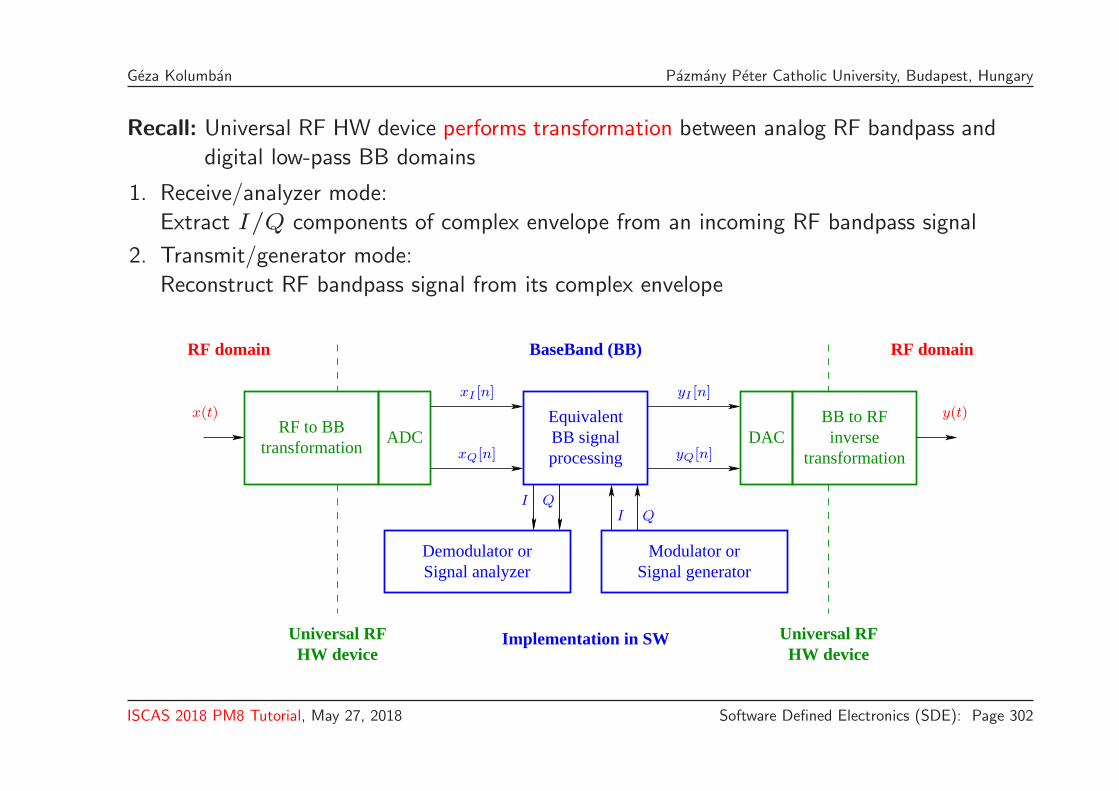
Recall: Universal RF HW device performs transformation between analog RF bandpass and
digital low-pass BB domains
1. Receive/analyzer mode:
Extract I/Q components of complex envelope from an incoming RF bandpass signal
2. Transmit/generator mode:
Reconstruct RF bandpass signal from its complex envelope
EquivalentBB signalprocessing
BaseBand (BB)
BB to RFinverse
transformation
RF domain
RF to BBtransformation
RF domain
Signal analyzer Signal generator
Universal RFHW device
Implementation in SW Universal RFHW device
Demodulator or Modulator or
ADC DAC
I QQI
y(t)
xI [n]
xQ[n]
yI [n]
yQ[n]
x(t)
ISCAS 2018 PM8 Tutorial, May 27, 2018 Software Defined Electronics (SDE): Page 302

Geza Kolumban Pazmany Peter Catholic University, Budapest, Hungary
Transformations to be performed by the universal HW Devices
RF to BB transformation
x(t) ⇒ xI[n] and xQ[n]
ADC
ADC-2
2
sin(ωct)
cos(ωct)x(t)
xI [n]
xQ[n]
xI(t)
xQ(t)
BB to RF transformation
xI[n] and xQ[n] ⇒ x(t)
DAQ
DAQ
−
+
cos(ωct) x(t)
sin(ωct)
xI [n]
xQ[n]
xI(t)
xQ(t)
ISCAS 2018 PM8 Tutorial, May 27, 2018 Software Defined Electronics (SDE): Page 303

Geza Kolumban Pazmany Peter Catholic University, Budapest, Hungary
3 Key HW component: The universal RF hardware device(Transformation between the analog RF bandpass and digital low-pass BBdomains)
Universal RF HW device can be considered as the circuit implementation of mathematical
transformation performed between RF and BB domains
Main requirement: Be universal, i.e., be suitable for the implementation of every communi-
cations and measurement applications without any modification
TOPICS TO BE DISCUSSED:
3.1 Universal Software Radio Peripheral (USRP)
3.2 PXIe-based universal Software Defined (SD) wireless RF platform
3.3 Integrated circuits
ISCAS 2018 PM8 Tutorial, May 27, 2018 Software Defined Electronics (SDE): Page 304

Geza Kolumban Pazmany Peter Catholic University, Budapest, Hungary
3.1 Universal Software Radio Peripheral (USRP)
USRP device:
• Receive path: 14-bit ADC
SQNR ≤ 84 dB
• Transmit path: 16-bit DAC
• Up to 50 MS/s Gigabit
Ethernet Streaming
• RF bandwidth ∼40 MHz
• Low accuracy and stability,
developed for university ed-
ucation and amateurs
Testing a 915-MHz FSK radio link where the USRP device
is used to implement the FSK receiver
ISCAS 2018 PM8 Tutorial, May 27, 2018 Software Defined Electronics (SDE): Page 305

Geza Kolumban Pazmany Peter Catholic University, Budapest, Hungary
Block diagram of the USRP device
Main components: • Main board, includes DACs, ADCs, FPGA
• Exchangeable RF daughter board (up to 6 GHz, analog RF circuits)
PLL VCO
Rx
Con
trol
Tx
Con
trol
Gig
aBit
Eth
erne
t
40 MHz
40 MHzPLL VCO
40 MHz
40 MHz
RF Switch
Drive AmpLNARF Switch
Rx1
Tx1
Rx2
Tx Amp
+
+
ADC
ADC
DAC
DACsample
Up−
Up−
sample
sample
Down−
Down−
sample
Main board
400 MS/s
400 MS/s
100 MS/s
100 MS/s
π2
0
π2
0
Reconstruction of RFbandpass signal
cos(ωct)
sin(ωct)
xI(t)
xQ(t)
x(t)
+
−
Extraction of complexenvelope
-2
2
sin(ωct)
cos(ωct)x(t)
xI(t)
xQ(t)
Important advantage of USRP device: Drivers are available
ISCAS 2018 PM8 Tutorial, May 27, 2018 Software Defined Electronics (SDE): Page 306

Geza Kolumban Pazmany Peter Catholic University, Budapest, Hungary
3.2 PXIe-based universal SDE wireless RF platform
Testing a 2.4-GHz FM-DCSK radio link over an indoor
noisy multipath channel PXI Systems Alliance:
• PCI eXtensions for Instrumenta-tion (PXI) is modular instrumen-
tation architecture developed toimplement test equipment and
automation system
• Many different modules are
available
• Any kind of test beds can be
built from the modules
• PXI provides accuracy and sta-
bility required in measurementengineering and professional ap-
plications
Important advantage of PXIe test bed: Drivers are available
ISCAS 2018 PM8 Tutorial, May 27, 2018 Software Defined Electronics (SDE): Page 307

Geza Kolumban Pazmany Peter Catholic University, Budapest, Hungary
Main components of a PXIe-based test bed
1
2 3.1 3.2
1 Chassis
2 Embedded controller
built with the same ar-
chitecture as a multi-
core PC (on the left)
3 Different modules
3.1 Vector signal ana-
lyzer (in the middle)
Extract I/Q
3.2 Vector signal gener-
ator (on the right)
Reconstruct RF
Operation principle of the PXIe-based universal SD HW platform:
• Heterodyne receive and transmit RF frontends
• ADC and DAC conversions are performed in the IF frequency band
ISCAS 2018 PM8 Tutorial, May 27, 2018 Software Defined Electronics (SDE): Page 308

Geza Kolumban Pazmany Peter Catholic University, Budapest, Hungary
Receive mode: Operation principle of an IF digitizer
Recall:
Extraction of com-
plex envelope
-2
2
sin(ωct)
cos(ωct)x(t)
xI(t)
xQ(t)
Note: • IF bandpass signal is digitized first
• I/Q components of complex envelope are extracted in the digital domain
• Low-pass filtering and decimation of I/Q components are performed
• On-board memory is available for off-line signal processing
ISCAS 2018 PM8 Tutorial, May 27, 2018 Software Defined Electronics (SDE): Page 309

Geza Kolumban Pazmany Peter Catholic University, Budapest, Hungary
Transit mode: Operation principle of an IF arbitrary waveform generator
Recall:
Reconstruction of
RF bandpass signal
−
+
cos(ωct)
sin(ωct)
xI(t)
xQ(t)
x(t)
Note: • Arbitrary waveform is generated from its complex envelope calculated off-line and
uploaded into the Waveform Memory
• RF bandpass signal is reconstructed in the digital domain
ISCAS 2018 PM8 Tutorial, May 27, 2018 Software Defined Electronics (SDE): Page 310

Geza Kolumban Pazmany Peter Catholic University, Budapest, Hungary
3.3 Integrated circuits available on the market• Analog Devices: Analog inputs and outputs, operating from 50 MHz up to 2.2 GHz
• Maxim MAX2769 with built-in analog-to-digital converter
• Analog Devices: AD9361, a complete universal HW RF transformer
Analog Devices: AD8347
Block diagram of AD8347
Note: Low-pass filters are not included
Recall: Extraction of I/Q components
-2
2
sin(ωct)
cos(ωct)x(t)
xI(t)
xQ(t)
ISCAS 2018 PM8 Tutorial, May 27, 2018 Software Defined Electronics (SDE): Page 311
Geza Kolumban Pazmany Peter Catholic University, Budapest, Hungary
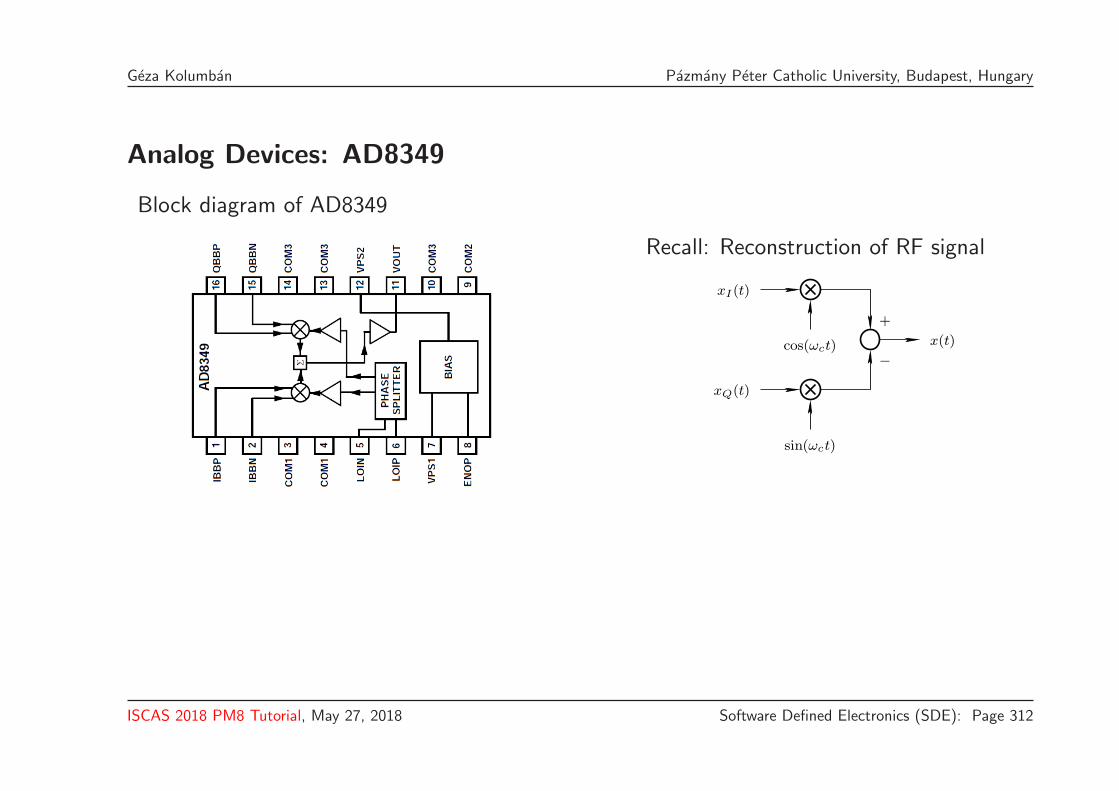
Analog Devices: AD8349
Block diagram of AD8349
Recall: Reconstruction of RF signal
−
+
cos(ωct)
sin(ωct)
xI(t)
xQ(t)
x(t)
ISCAS 2018 PM8 Tutorial, May 27, 2018 Software Defined Electronics (SDE): Page 312

Geza Kolumban Pazmany Peter Catholic University, Budapest, Hungary
Maxim IC with built-in digitizer (Price: US$5.00/1 pc or US$3.45/500 pcs)
MAX2769 with digital I/Q outputs
Recall: Extraction of complex
envelope
-2
2
sin(ωct)
cos(ωct)x(t)
xQ(t)
xI(t)
ADC
ADC
xI [n]
xQ[n]
ISCAS 2018 PM8 Tutorial, May 27, 2018 Software Defined Electronics (SDE): Page 313

Geza Kolumban Pazmany Peter Catholic University, Budapest, Hungary
Analog Devices: AD9361, a complete universal HW RF transformer
Main parameters:
• Digital input and output
• Tx: 47 MHz–6GHz
• Rx: 70 MHz–6GHz
• 200 kHz≤BW≤56 MHz, tunable
• 12-bit DACs
• 12-bit ADCs
ISCAS 2018 PM8 Tutorial, May 27, 2018 Software Defined Electronics (SDE): Page 314

Geza Kolumban Pazmany Peter Catholic University, Budapest, Hungary
Contents:
1 Motivation and a new way of teaching and researching ICT systems
2 Theoretical background2.1 Concept of complex envelopes
2.2 Derivation of BaseBand (BB) equivalents
3 Key HW component: The universal RF hardware device(Transformation between the analog RF bandpass and digital low-pass BB domains)
4 Embedded operation of universal HW transformer
5 Applications of equivalent baseband information processing5.1 Computer simulations
5.2 Industrial applications
5.3 Application in scientific research
6 Conclusions and acknowledgements
ISCAS 2018 PM8 Tutorial, May 27, 2018 Software Defined Electronics (SDE): Page 401

Geza Kolumban Pazmany Peter Catholic University, Budapest, Hungary
TOPICS TO BE DISCUSSED:
4.1 A similar problem:Architecture of OSI-BR compliant IEEE Std. 802 protocol stack
4.2 Embedded operation of a generic universal HW transformer
4.3 Examples: • USRP device
• PXIe-based universal RF HW platform
ISCAS 2018 PM8 Tutorial, May 27, 2018 Software Defined Electronics (SDE): Page 402

Geza Kolumban Pazmany Peter Catholic University, Budapest, Hungary
4.1 Architecture of IEEE Std. 802 protocol stack
Operation principle is defined
by the Open System Intercon-
nection (OSI) Basic Reference
(BR) model in computer net-
works
Note, two Service Access
Points (SAPs) are defined
(1) PD-SAP:
Physical (PHY) layer Data
(Transmission of data)
(2) PLME-SAP:
Physical Layer Management
Entity (Configuration)
ISCAS 2018 PM8 Tutorial, May 27, 2018 Software Defined Electronics (SDE): Page 403

Geza Kolumban Pazmany Peter Catholic University, Budapest, Hungary
4.2 Embedded operation of a universal HW transformer
SDE protocol stack is similar to that of the IEEE Std. 802
Device
Address Session
Open
Device control chain
Close
SessionUniversal HW transformer
Complex waveform Configuration
BR model
OSI BRApplication Layer
SAP1 SAP2
Universal HW transformer provides services for the upper (application) layer of host computer
Note the two service points:
• SAP1: Upload (Tx) or fetch (Rx) data of complex waveform
• SAP2: Set configuration parameters
ISCAS 2018 PM8 Tutorial, May 27, 2018 Software Defined Electronics (SDE): Page 404
Geza Kolumban Pazmany Peter Catholic University, Budapest, Hungary
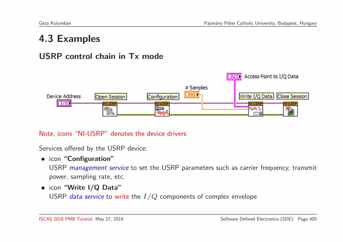
4.3 Examples
USRP control chain in Tx mode
Note, icons “NI-USRP” denotes the device drivers
Services offered by the USRP device:
• icon “Configuration”
USRP management service to set the USRP parameters such as carrier frequency, transmit
power, sampling rate, etc.
• icon “Write I/Q Data”
USRP data service to write the I/Q components of complex envelope
ISCAS 2018 PM8 Tutorial, May 27, 2018 Software Defined Electronics (SDE): Page 405

Geza Kolumban Pazmany Peter Catholic University, Budapest, Hungary
Control chain in 4-FSK transmitter discussed in Section 1
Good news: the structure of control chain is the same for each HW transformer:
Select the HW device to be used ⇒ Open session ⇒ Configure HW transformer ⇒ Upload or
fetch complex waveform ⇒ Close session ⇒ Visualize Error Message (if any)
ISCAS 2018 PM8 Tutorial, May 27, 2018 Software Defined Electronics (SDE): Page 406
Geza Kolumban Pazmany Peter Catholic University, Budapest, Hungary
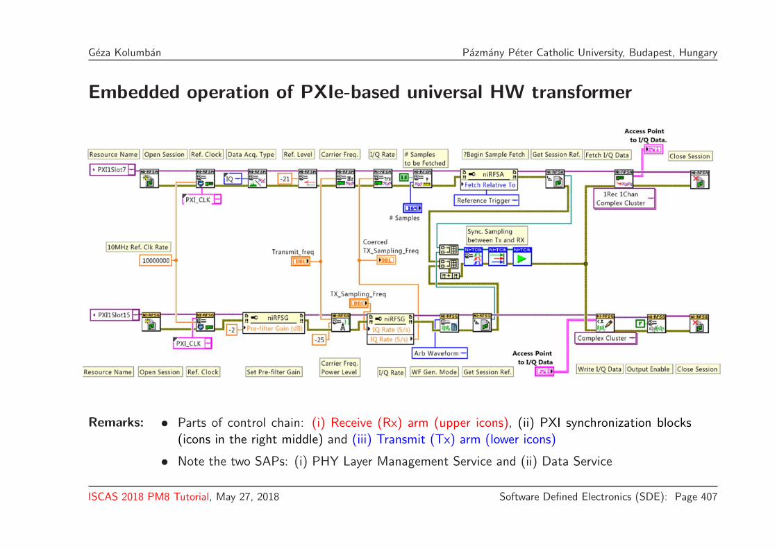
Embedded operation of PXIe-based universal HW transformer
Remarks: • Parts of control chain: (i) Receive (Rx) arm (upper icons), (ii) PXI synchronization blocks(icons in the right middle) and (iii) Transmit (Tx) arm (lower icons)
• Note the two SAPs: (i) PHY Layer Management Service and (ii) Data Service
ISCAS 2018 PM8 Tutorial, May 27, 2018 Software Defined Electronics (SDE): Page 407

Geza Kolumban Pazmany Peter Catholic University, Budapest, Hungary
Contents:
1 Motivation and a new way of teaching and researching ICT systems
2 Theoretical background2.1 Concept of complex envelopes
2.2 Derivation of BaseBand (BB) equivalents
3 Key HW component: The universal RF hardware device(Transformation between the analog RF bandpass and digital low-pass BB domains)
4 Embedded operation of universal HW transformer
5 Applications of equivalent baseband information processing5.1 Computer simulations
5.2 Industrial applications
5.3 Application in scientific research
6 Conclusions and acknowledgements
ISCAS 2018 PM8 Tutorial, May 27, 2018 Software Defined Electronics (SDE): Page 501

Geza Kolumban Pazmany Peter Catholic University, Budapest, Hungary
5 Applications of equivalent baseband information processing
5.1 Computer simulations
Goal: Minimize computer simulation time by minimizing sampling rate
BB equivalents are used in each computer simulator
One example from the LabVIEW Modulation Toolkit
Zoom-in the block ofRF bandpass signalreconstruction
ISCAS 2018 PM8 Tutorial, May 27, 2018 Software Defined Electronics (SDE): Page 502

Geza Kolumban Pazmany Peter Catholic University, Budapest, Hungary
5.2 Industrial applications
Why SDE?
• Implementation in SW offers a huge level of flexibility
• Low prototyping and production cost, minimizing time-to-market
• In many applications adaptivity is a must
• Certain applications such as cognitive radio rely on multifunctional use ofthe same HW platform
• Continuous and rapid change in standards, technology and/or applicationscan be followed, deployed products already in use can be updated andmodernized by changing/updating the SW
• Market demands frequently cannot be identified/predicted in advance beforereleasing a new product. After evaluating the market response, new servicesand applications can be implemented on the already sold devices
ISCAS 2018 PM8 Tutorial, May 27, 2018 Software Defined Electronics (SDE): Page 503

Geza Kolumban Pazmany Peter Catholic University, Budapest, Hungary
5.2.1 RADIO COMMUNICATIONS
CMX994: Direct conversion or zero-IF receiver
Recall:
Generation of BB
I/Q components
-2
2
sin(ωct)
cos(ωct)x(t)
xI(t)
xQ(t)
Note: Complex envelope of received RF bandpass signal are provided as analog BB signals
ISCAS 2018 PM8 Tutorial, May 27, 2018 Software Defined Electronics (SDE): Page 504

Geza Kolumban Pazmany Peter Catholic University, Budapest, Hungary
CC2430: ISM-band SoC O-QPSK transceiver
Direct-conversion transmitter
LNA
DIGITAL
DEMODULATOR
- Digital RSSI- Gain Control
- Image Suppression- Channel Filtering
- Demodulation- Frame
synchronization
DIGITAL
MODULATOR
- Data spreading
- Modulation
AUTOMATIC GAIN CONTROL
TX POWER CONTROL
TXRX SWITCH
ADC
ADC
DAC
DAC
0
90
FREQ SYNTH
PowerControl
PA
FFCTRL
Register bus
CSMA/CA
STROBEPROCESSOR
RADIO
REGISTERBANK
RA
DIO
DA
TA
IN
TE
RF
AC
E
CO
NT
RO
L
LO
GIC
IRQHANDLING
SFR bus
Recall:
Reconstruction of
an RF signal
cos(ωct)
sin(ωct)
xI(t)
xQ(t)
x(t)
+
−
ISCAS 2018 PM8 Tutorial, May 27, 2018 Software Defined Electronics (SDE): Page 505

Geza Kolumban Pazmany Peter Catholic University, Budapest, Hungary
MAX2827: A dual-band IEEE 802.11g/a zero-IF receiver and direct-conversion transmitter
ISCAS 2018 PM8 Tutorial, May 27, 2018 Software Defined Electronics (SDE): Page 506

Geza Kolumban Pazmany Peter Catholic University, Budapest, Hungary
AD9361: A complete universal HW RF transformer includingADC/DAC converters
Main parameters:
• Digital input and output
• Tx: 47 MHz–6GHz
• Rx: 70 MHz–6GHz
• 200 kHz≤BW≤56 MHz, tunable
• 12-bit DACs
• 12-bit ADCs
Recall:
• Resolutions of ADC/DAC convert-
ers limit level of quantization noise
SQNR ≈ 6.02 × resolution
ISCAS 2018 PM8 Tutorial, May 27, 2018 Software Defined Electronics (SDE): Page 507
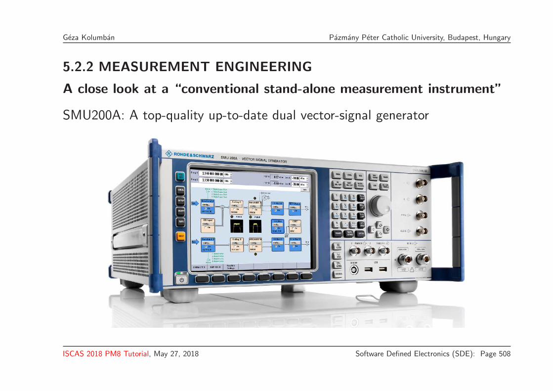
Geza Kolumban Pazmany Peter Catholic University, Budapest, Hungary
5.2.2 MEASUREMENT ENGINEERING
A close look at a “conventional stand-alone measurement instrument”
SMU200A: A top-quality up-to-date dual vector-signal generator
ISCAS 2018 PM8 Tutorial, May 27, 2018 Software Defined Electronics (SDE): Page 508

Geza Kolumban Pazmany Peter Catholic University, Budapest, Hungary
Note: • Today even the stand-alone type measurement instruments use the idea of virtual instrumentationwhere signal processing is done in BB
• Note the labels “Baseband A/B,” blocks “I/Q Mod A/B,” outputs “DIG I/Q OUT” and “I/Q OUT”
• However, there is no access to the modules of instruments and SW used in BB cannot be changed
ISCAS 2018 PM8 Tutorial, May 27, 2018 Software Defined Electronics (SDE): Page 509

Geza Kolumban Pazmany Peter Catholic University, Budapest, Hungary
5.2.2 OPTICAL COMMUNICATIONS
Note:
I/Q components of complex envelope
of received optical signal are extracted
and all signal processing from chan-
nel equalization to coherent detection
is performed in baseband
Pictures have been taken at the
Lab of Optical Communications
with the permission of Prof. Chao Lu
EIE Dept., The Hong Kong
Polytechnic University
ISCAS 2018 PM8 Tutorial, May 27, 2018 Software Defined Electronics (SDE): Page 510

Geza Kolumban Pazmany Peter Catholic University, Budapest, Hungary
Implementation of a 64-QAM coherent optical receiver in BB
By courtesy of Prof. Lu, EIE Dept., The Hong Kong Polytechnic University
Note the huge potential for standardization:
The same BB 64-QAM demodulator can be used in many different applications
ISCAS 2018 PM8 Tutorial, May 27, 2018 Software Defined Electronics (SDE): Page 511

Geza Kolumban Pazmany Peter Catholic University, Budapest, Hungary
5.3 Application in scientific research
Why to use the SDE approach in research?
• Results of scientific research are verified by computer simulations
• Today BB simulators are used almost exclusively for system level verification
• Goal: Turn the baseband simulator used in the research phase directlyinto a real working system capable of generating and receiving realRF signals
• Perform real field tests without building HW
• Measure physical signals and verify research results by stand-alone testequipment
• Important advantage: SW implementation makes easy and fast to performmodifications required during research and in prototyping
Example discussed here:
• Implementation of a chaos-based FM-DCSK radio communications systems
ISCAS 2018 PM8 Tutorial, May 27, 2018 Software Defined Electronics (SDE): Page 512

Geza Kolumban Pazmany Peter Catholic University, Budapest, Hungary
Generic interface among the different SW/HW components
• Both baseband simulators and universal RF HW transformers process complex envelopes
• Complex envelopes serve as generic interface points among the various SW/HW components
• Approach discussed here can be applied to all simulators which use complex envelopes
Baseband simulator Driver of universal
RF HW transformer
• BB simulator (on the left from
the vertical thick gray line)
generates the complex enve-
lope of FSK signal
• Via the “NI-USRP” driver this
complex waveform is trans-
formed into a real analog RF
bandpass signal by the univer-
sal RF HW device
• Complex waveform includes
timestamp (t0), sampling
time (dt) and complex enve-
lope
ISCAS 2018 PM8 Tutorial, May 27, 2018 Software Defined Electronics (SDE): Page 513

Geza Kolumban Pazmany Peter Catholic University, Budapest, Hungary
Implementation of chaos-based FM-DCSK on an RF PXIe-SDE platform
Goals: • Implement a real FM-DCSK transceiver that can transmit and receive real 2.4-GHz
microwave signals
• Implement (i) Additive White Gaussian (AWGN) and (ii) noisy multipath channel
conditions
• Evaluate the BER performance of FM-DCSK under various channels conditions
• Check all microwave signals with stand-alone test equipment
• Perform a real field test in a real indoor office environment
Main steps: • Develop a MATLAB baseband simulator for the FM-DCSKradio link including the different channel models
• Integrate MATLAB BB simulator into LabVIEWWhy LabVIEW? Because it offers drivers for the blocks of PXI HW platform
• Use PXIe-based universal SDE platform for implementation
ISCAS 2018 PM8 Tutorial, May 27, 2018 Software Defined Electronics (SDE): Page 514

Geza Kolumban Pazmany Peter Catholic University, Budapest, Hungary
Overview of chaos-based FM-DCSK telecommunications system
• Carrier signal is an inherently ultra-wideband chaotic signal
• Chaos-based communications is an alternative solution to spread spectrum communications
where there is no need for an extra spectrum spreading signal
• Typical application: Indoor multipath channels
Modulation scheme
• g(t) is an FM signal where the modulating signal is
provided by a chaotic signal generator
• Each bit is carried by two waveforms of duration Tb/2.
These are reference and information bearing waveforms
• Information is carried by the correlation of reference and
information bearing waveforms
Tb/2
Tb
t
g(t)
g(t− Tb
2) for bit 1
−g(t− Tb
2) for bit 0
Block diagram of FM-DCSK
autocorrelation receiverfilter
Channel
h(t)Delay
circuit
Decision∫τ· dt
r(t) r(t) z(t)
T/2
bi
ISCAS 2018 PM8 Tutorial, May 27, 2018 Software Defined Electronics (SDE): Page 515

Geza Kolumban Pazmany Peter Catholic University, Budapest, Hungary
Step 1: Derivation of MATLAB BB simulator for FM-DCSK radio link
Block diagram of an RF FM-DCSK radio link
Recovered
information
De ision
ir uit
T
Threshold
bi
Delay
T/2
Tele ommu-
ni ations
hannel
Radio hannelFM-DCSK modulator
Binary information
to be transmitted
bi
FM
mod
DCSK
mod
Low − pass
chaotic
signal
m(t)
∫T/2 . dt
Channel �lter FM-DCSK auto orrelation re eiver
z(t)
input
r(t)
Demodulatorinput
r(t)
Receiveroutput
Modulator
s(t)y(t)
Low − passobservation signal
• To get the equivalent BB model, low-pass observation signal z(t) has to be expressed as a
function of low-pass chaotic signal m(t)
• Recall: – Cascading is preserved in baseband
– BB equivalents of many blocks are available as library elements
• BB equivalent of autocorrelation detector has to be derived
ISCAS 2018 PM8 Tutorial, May 27, 2018 Software Defined Electronics (SDE): Page 516

Geza Kolumban Pazmany Peter Catholic University, Budapest, Hungary
Derivation of BB equivalent of autocorrelation detector
t∫
t−T/2
· dτ
z(t)
T
Threshold
Decision
circuit
Delay
T/2
Correlator
r(t)
noisy signal
Received
bi
Estimated
bits
r(t)
Detection algorithm of FM-DCSK receiver
z(t) =
t∫
t−T/2
r(t)r(t −T
2) dt ≈
t∫
t−T/2
r(t)r(t −T
2) dt
where r(t) = rI(t) cos(ωct) − rQ(t) sin(ωct) (canonical form)
Goal: Express z(t) as a function of rI(t) and rQ(t), i.e., the complex envelope of received
noisy signal r(t)
Note: z(t), rI(t) and rQ(t) are all BB low-pass signals
ISCAS 2018 PM8 Tutorial, May 27, 2018 Software Defined Electronics (SDE): Page 517

Geza Kolumban Pazmany Peter Catholic University, Budapest, Hungary
Substitution of the detector input
r(t) = rI(t) cos(ωct) − rQ(t) sin(ωct)
into the detection algorithm
z(t) =
t∫
t−T/2
r(t)r(t −T
2) dt
gives
z(t) =t∫
t−T/2
rI(t)rI(t −T2 ) cos(ωct) cos[ωc(t −
T2 )] dt
−t∫
t−T/2
rI(t)rQ(t −T2 ) cos(ωct) sin[ωc(t −
T2 )] dt
−t∫
t−T/2
rQ(t)rI(t −T2 ) sin(ωct) cos[ωc(t −
T2 )] dt
+t∫
t−T/2
rQ(t)rQ(t −T2 ) sin(ωct) sin[ωc(t −
T2 )] dt
ISCAS 2018 PM8 Tutorial, May 27, 2018 Software Defined Electronics (SDE): Page 518

Geza Kolumban Pazmany Peter Catholic University, Budapest, Hungary
Considering that • ωc T/2 = 2πi where i is an integer and
• exploiting the trigonometric identities
the following equation is obtained
z(t) =t∫
t−T/2
rI(t)rI(t −T2 ) cos
2(ωct) dt − . . .
=t−T/2+Tc/2
∫
t−T/2
rI(t)rI(t −T2 )
1+cos(2ωct)2 dt +
t−T/2+2Tc/2∫
t−T/2+Tc/2
rI(·)rI(·)1+cos(2ωct)
2 dt + . . .
= 12
rI(t)rI(t −T2 )
t−T/2+Tc/2∫
t−T/2
1dt + rI(t)rI(t −T2 )
t−T/2+Tc/2∫
t−T/2
cos(2ωct)dt + . . .
This can be simplified further because the complex envelope is a slowly varying function
z(t) =1
2
[
t∫
t−T/2
rI(t)rI(t −T
2) dt +
t∫
t−T/2
rQ(t)rQ(t −T
2) dt
]
ISCAS 2018 PM8 Tutorial, May 27, 2018 Software Defined Electronics (SDE): Page 519
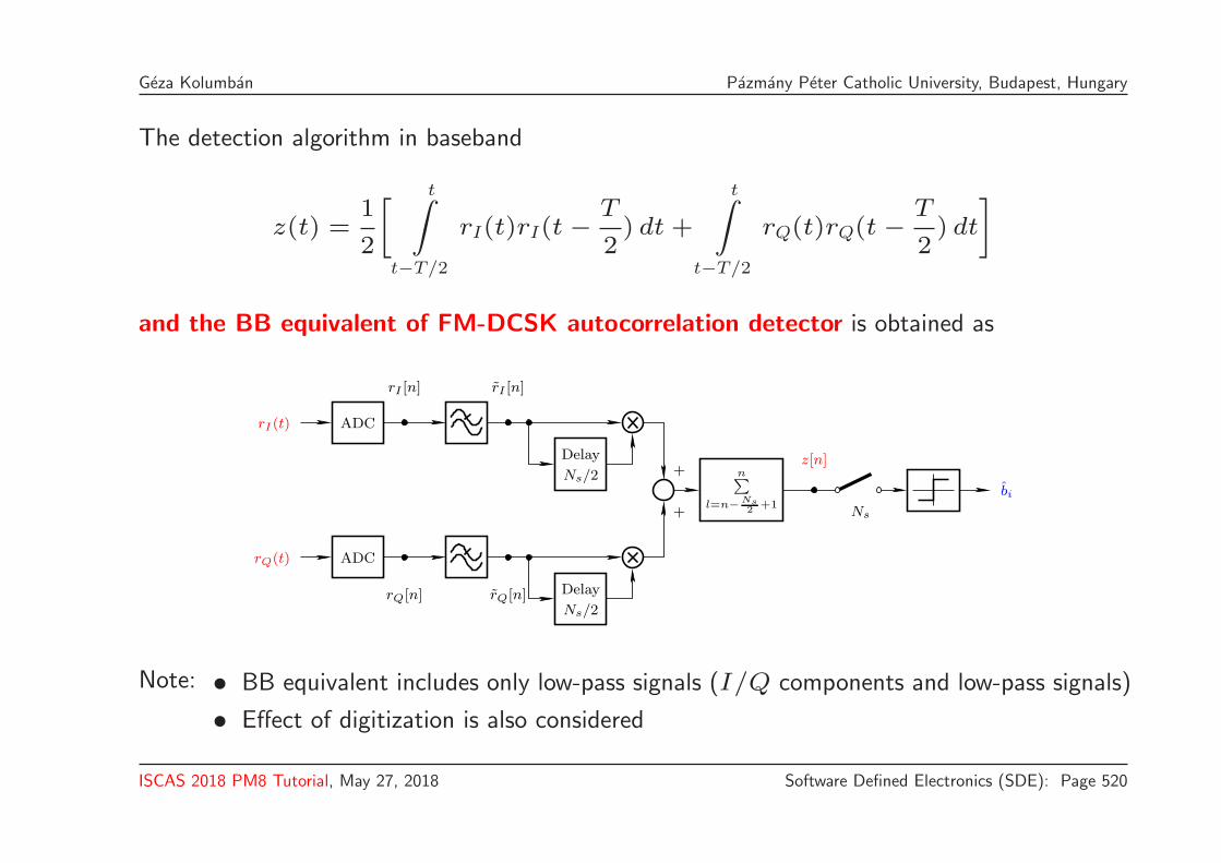
Geza Kolumban Pazmany Peter Catholic University, Budapest, Hungary
The detection algorithm in baseband
z(t) =1
2
[
t∫
t−T/2
rI(t)rI(t −T
2) dt +
t∫
t−T/2
rQ(t)rQ(t −T
2) dt
]
and the BB equivalent of FM-DCSK autocorrelation detector is obtained as
Delay
Ns/2
Delay
Ns/2 +
+
z[n]
rI [n]
rQ[n]
rI [n]
rQ[n]
n∑
l=n−
Ns
2+1
ADC
ADC
rI(t)
rQ(t)
Ns
bi
Note: • BB equivalent includes only low-pass signals (I/Q components and low-pass signals)
• Effect of digitization is also considered
ISCAS 2018 PM8 Tutorial, May 27, 2018 Software Defined Electronics (SDE): Page 520

Geza Kolumban Pazmany Peter Catholic University, Budapest, Hungary
MATLAB BB simulator of an FM-DCSK radio link
KK
Delay
T/2
Delay
T/2nQ(t)
nI(t)
DCSK
mod
mod
DCSK
yI (t)
yQ(t)
sI(t)
sQ(t)
AWGN hannel
Ac cos(·)
Ac cos(·)
m(t)
1
2hI(t)
1
2hI(t)
∫T/2
(·)dt
∫T/2
(·)dt
1
2
DCSK MOD
2πkft∫
0
(·)dτ bi
rI(t)rI (t)
rQ(t)rQ(t)
z(t)
FM transmitter FM-DCSK auto orrelation re eiverChannel �lter
• MATLAB subroutines have been developed for each block of the FM-DCSK radio link in BB
• Recall: Cascading is preserved in the baseband, consequently library elements can be used
• Even the various propagation condition in radio channel can be implemented in baseband
ISCAS 2018 PM8 Tutorial, May 27, 2018 Software Defined Electronics (SDE): Page 521

Geza Kolumban Pazmany Peter Catholic University, Budapest, Hungary
Step 2:
Integration of MATLAB BB simulator into the PXIe-based SDE platform
Goal and tools available:
• Turn MATLAB BB simulator developed for research into an operatingFM-DCSK radio link without any extra efforts
• Recall, transformation between I/Q sequences given in BB and physical RFanalog bandpass signals is performed by the universal HW device
• LabVIEW offers all drivers required by the universal HW transformers
Solution:
• Integrate MATLAB BB simulator into LabVIEW platform
Method:
• As discussed I/Q components of complex envelope provide the genericinterface between the different SW/HW platforms
ISCAS 2018 PM8 Tutorial, May 27, 2018 Software Defined Electronics (SDE): Page 522

Geza Kolumban Pazmany Peter Catholic University, Budapest, Hungary
Integration of MATLAB BB simulator into the PXIe-based SDE platform
Note: • Observe, both channel filtering and FM-DCSK autocorrelation demodulator are implemented
in MATLAB. See the MATLAB script on the top
ISCAS 2018 PM8 Tutorial, May 27, 2018 Software Defined Electronics (SDE): Page 523

Geza Kolumban Pazmany Peter Catholic University, Budapest, Hungary
Step 3: Implementation on PXIe-based universal SDE wireless platform
• Testing of a 2.4-GHz FM-DCSK radio transceiver in a noisy multipath channel
• Checking by a stand-alone test equipment is always must in verification
Note: The spectra measured in RF bandpass and calculated in BB domains are identical
ISCAS 2018 PM8 Tutorial, May 27, 2018 Software Defined Electronics (SDE): Page 524

Geza Kolumban Pazmany Peter Catholic University, Budapest, Hungary
Unique features of SDE implementation
• Addition to the FM-DCSK transmitter many additional functions and/orsignal processing blocks can be implemented
– Channel noise, multipath propagation, interference, etc
• Any kind of test equipment can be implemented and any kind of measure-ments can be performed
– Multifunctionality can be implemented, for example, signal reception andmeasurement of received spectrum can be done simultaneously
• Automated test beds can be implemented
• Both the system configuration and system parameters can be changed easilyin software
ISCAS 2018 PM8 Tutorial, May 27, 2018 Software Defined Electronics (SDE): Page 525

Geza Kolumban Pazmany Peter Catholic University, Budapest, Hungary
Multifunctionality and flexibility of SDE implementation
Note, the same received waveform is used simultaneously to (i) recover the transmitted
information and (ii) measure the spectrum of received signal
ISCAS 2018 PM8 Tutorial, May 27, 2018 Software Defined Electronics (SDE): Page 526

Geza Kolumban Pazmany Peter Catholic University, Budapest, Hungary
Time consuming measurements can be automatized
(Front panel of PXIe-based Universal Software Defined Wireless Platform)
Note: • Left solid curve: Theoretical value of Bit Error Rate (BER))
• Right solid curve: BER measured in the universal SW defined wireless platform
• Implementation error is about 0.7 dB
ISCAS 2018 PM8 Tutorial, May 27, 2018 Software Defined Electronics (SDE): Page 527

Geza Kolumban Pazmany Peter Catholic University, Budapest, Hungary
Verification of the PXIe-based Universal SD Wireless Platform
Automated BER evaluation:
FM-DCSK, 2B = 17 MHz, T = 2 µs
Theoretical noise performance:
BER =1
22Bτexp
(
−Eb
2N0
) 2Bτ−1∑
i=0
(
Eb2N0
)i
i!
×
2Bτ−1∑
j=i
1
2j
(
j + 2Bτ − 1j − i
)
Legend:
• Solid curve: BER given by the analytical expression
shown above
• ‘+’ marks: BER measured by automated platform
in the 2.4-GHz ISM frequency band
Remarks: • Implementation loss is about 0.7 dB (noise of contribution of universal HW trans-
former, quantization noise, etc)
• Measurement time up to BER= 10−7 is about 3 hours
ISCAS 2018 PM8 Tutorial, May 27, 2018 Software Defined Electronics (SDE): Page 528

Geza Kolumban Pazmany Peter Catholic University, Budapest, Hungary
Automated BER performance evaluation of FM-DCSK in indoor office environment
Spectrum of transmitted
FM-DCSK signal
(Modulation: Random bit
stream)
Spectrum of received signal and BER performance
Effects of multipath related frequency selective deep fadings
are clearly shown in the upper figure
ISCAS 2018 PM8 Tutorial, May 27, 2018 Software Defined Electronics (SDE): Page 529

Geza Kolumban Pazmany Peter Catholic University, Budapest, Hungary
Contents:
1 Motivation and a new way of teaching and researching ICT systems
2 Theoretical background2.1 Concept of complex envelopes
2.2 Derivation of BaseBand (BB) equivalents
3 Key HW component: The universal RF hardware device(Transformation between the analog RF bandpass and digital low-pass BB domains)
4 Embedded operation of universal HW transformer
5 Applications of equivalent baseband information processing5.1 Computer simulations
5.2 Industrial applications
5.3 Application in scientific research
6 Conclusions and acknowledgements
ISCAS 2018 PM8 Tutorial, May 27, 2018 Software Defined Electronics (SDE): Page 601

Geza Kolumban Pazmany Peter Catholic University, Budapest, Hungary
6 Conclusions and acknowledgements
TOPICS TO BE DISCUSSED:
6.1 Features of SDE concept
6.2 New challenges for the IEEE Circuits and Systems Society
6.3 A new way of and a new focus in teaching ICT systems
6.4 Acknowledgements
ISCAS 2018 PM8 Tutorial, May 27, 2018 Software Defined Electronics (SDE): Page 602

Geza Kolumban Pazmany Peter Catholic University, Budapest, Hungary
6.1 Features of SDE concept
• HW and SW components are completely separated in SDE and a universal
HW device is used to perform the transformations between the RF and BBdomains
• Every application is implemented entirely in SW, consequently, SDE offersa very flexible solution where every property from the modulation scheme totelecommunications parameters can be changed even dynamically
• Since the transmitted and received signals can be also considered as testsignals, testing of radio transceiver and channel conditions can be performedparallel to radio communications without interrupting the data traffic
• Key issue: The same HW is used in each application
• SDE offers an ideal implementation platform for cognitive radio and recon-figurable adaptive systems
ISCAS 2018 PM8 Tutorial, May 27, 2018 Software Defined Electronics (SDE): Page 603

Geza Kolumban Pazmany Peter Catholic University, Budapest, Hungary
Features of SDE — cont’d
• In research, SDE offers a unified test bed for verification of new theoriesand applications
• In prototyping, SDE reduces the time-to-market considerably
• Application of SDE concept makes the development of RF/microwave/opticalcircuits, the HW components, “unnecessary”
• Provides an easy way for updating the already deployed ICT systems andcomponents
• Because all real analog RF/microwave signals are available, real field tests
can be performed
• Computer simulators can be turned directly (without any modification andextra work) into a working ICT system
• Because SDE systems are embedded systems, they can be integrated intoautomated test beds, calibration systems and manufacturing lines
ISCAS 2018 PM8 Tutorial, May 27, 2018 Software Defined Electronics (SDE): Page 604

Geza Kolumban Pazmany Peter Catholic University, Budapest, Hungary
What is new in SDE concept?
• Integration of many many subjects into one unified framework
– Theory of complex envelope, mathematical background
– Software Defined Radio (SDE)
– Virtual Instrumentation (VI)
– Embedded operation
• Concept of equivalent baseband transformation– It offers a unified theory for the design of all RF bandpass systems
– Instead of a case-by-case solution, SDE offers a general and systematic approach
– Transformation is performed by universal application-independent HW devices
• Implementation and derivation tool– Systematic way for the derivation of BB equivalent
• A new way of researching, teaching, developing, manufacturing and main-taining of ICT systems. A complete change in ICT paradigm where focusis shifted from circuit design to system level and SW-based approach
ISCAS 2018 PM8 Tutorial, May 27, 2018 Software Defined Electronics (SDE): Page 605
Geza Kolumban Pazmany Peter Catholic University, Budapest, Hungary
6.2 New challenges and research possibilities for the IEEE
Circuits and Systems Society
• Time available to detect a symbol in 256-QAM@ 1 Gbit/s is less than 8 ns
• High-speed FPGA devices are resource-limited computing devices
– where fixed-point number representation and fixed-point arithmetics are used
– fixed-point number representation and fixed-point arithmetics have some serious limita-
tions but also offers new opportunities in the algorithm design
– · · ·
• New algorithms optimized for FPGA BB implementation have to be developed
• New design rules for HW-SW co-design should be developed A lot of room for research
and many new challenges for the IEEE CAS Society
We are witnessing a revolution that will make a complete change in the design
paradigm of RF and microwave systems
ISCAS 2018 PM8 Tutorial, May 27, 2018 Software Defined Electronics (SDE): Page 606

Geza Kolumban Pazmany Peter Catholic University, Budapest, Hungary
6.3 A new way of and a new focus in teaching ICT systems
In education and Ph.D. research the change in EE-ICT paradigm is inevitable:
• End-of-roadmap has been almost reached in electrical engineering and ICT
• HW research, design and production are concentrated in a very few placesworldwide
• Except those very few lucky places the market demand worldwide is insystem level design and integration
• SDE approach gives a new chance for researching and developing new ICTsystems everywhere, it needs only a very little financial investment
ISCAS 2018 PM8 Tutorial, May 27, 2018 Software Defined Electronics (SDE): Page 607

Geza Kolumban Pazmany Peter Catholic University, Budapest, Hungary
Consequently, the waste majority of our graduates will work on
systems and system level integration
SDE can help because it can change EE teaching paradigm completely
• Conventional approach:
– Different subjects are taught independently of each other with different terminologies
– Young unexperienced students are expected to learn, understand and do the system level
design and integration themselves without any guidance
• New approach:
– Teach the curriculum in an opposite way
– After laying down the foundations start with system level engineering
– Teach all constituting topics from computer science to microwaves but only in that extent
which is necessary in system level engineering, BUT, in an integrated manner
• A new, integrated approach is badly needed in education
Instead of teaching the different subjects in an isolated manner, a system-level and
SW-based approach should be used everywhere
ISCAS 2018 PM8 Tutorial, May 27, 2018 Software Defined Electronics (SDE): Page 608
Geza Kolumban Pazmany Peter Catholic University, Budapest, Hungary
6.3 Acknowledgments
Many programs used in this tutorial have been developed by
Mr. Tamas Istvan Krebesz, my Ph.D. student
The research presented here has been carried out within the project Thematic Re-search Cooperation Establishing Innovative Informatic and Info-CommunicationSolutions, which has been supported by the European Union and co-financedby the European Social Fund under grant number EFOP-3.6.2-16-2017-00013.
ISCAS 2018 PM8 Tutorial, May 27, 2018 Software Defined Electronics (SDE): Page 609
Geza Kolumban Pazmany Peter Catholic University, Budapest, Hungary
Many thanks for your kind attention
ISCAS 2018 PM8 Tutorial, May 27, 2018 Software Defined Electronics (SDE): Page 610


