

Copyright
by
Minjung Kim
2014

The Dissertation Committee for Minjung Kimcertifies that this is the approved version of the following dissertation:
Ab initio simulation methods for the electronic and
structural properties of materials applied to molecules,
clusters, nanocrystals, and liquids.
Committee:
James R. Chelikowsky, Supervisor
Alexander A. Demkov
John G. Ekerdt
Gyeong S. Hwang
Brian A. Korgel

Ab initio simulation methods for the electronic and
structural properties of materials applied to molecules,
clusters, nanocrystals, and liquids.
by
Minjung Kim, B.S.
DISSERTATION
Presented to the Faculty of the Graduate School of
The University of Texas at Austin
in Partial Fulfillment
of the Requirements
for the Degree of
DOCTOR OF PHILOSOPHY
THE UNIVERSITY OF TEXAS AT AUSTIN
May 2014

To my parents,
Kim Dong-Ju and Kim Kun-Hea.

Acknowledgments
It is a great pleasure to acknowledge the ones who have shared my time throughout
my PhD journey.
First of all, I would like to express my profound gratitude to my advisor, Dr. Jim
Chelikowsky. He has provided tremendous support and given me freedom to explore
a wide range of interesting problems. He has never made me feel as if there were a
barrier between him and me. His kindness and valuable advice will not be forgotten.
I would also like to thank our research group members: Grady Schofield, Ben Garrett,
Alex Lee, Charles Lena, Scotty Bobbitt, and Jaime Souto. I must also acknowledge
two previous postdoctoral researchers, Dr. Khoong Hong Khoo and Dr. Noa Marom.
Part of my work could not have been completed without their help.
There are many names that I would like to acknowledge outside of the research group,
but I will limit myself to just a few:
To Greg and Mary Jane Grooms at the Hill House for their love and prayers.
To my best friends, Jisun Kim, So Youn Kim, Hee Jeong Oh, Szu-Hua Chen, Shruthi
Viswanath, Myoung Ji Jang, and Rachel Breeding.
Very special thanks to Katelyn Bobbitt for her close friendship and encouragement.
I will never forget the time spent with her (and her husband as well).
To my parents and brother, and in-laws. Their love and faith have made this thesis
v

possible.
Lastly, I would like to thank Hyunwook Kwak, for his tremendous support and en-
couragement.
vi

Ab initio simulation methods for the electronic and
structural properties of materials applied to molecules,
clusters, nanocrystals, and liquids.
Publication No.
Minjung Kim, Ph.D.
The University of Texas at Austin, 2014
Supervisor: James R. Chelikowsky
Computational approaches play an important role in today’s materials science
owing to the remarkable advances in modern supercomputing architecture and algo-
rithms. Ab initio simulations solely based on a quantum description of matter are
now very able to tackle materials problems in which the system contains up to a
few thousands atoms. This dissertation aims to address the modern electronic struc-
ture calculation methods applied to a range of various materials such as liquid and
amorphous phase materials, nanostructures, and small organic molecules. Our simu-
lations were performed within the density functional theory framework, emphasizing
the use of real-space ab initio pseudopotentials. On the first part of our study, we per-
formed liquid and amorphous phase simulations by employing a molecular dynamics
technique accelerated by a Chebyshev-subspace filtering algorithm. We applied this
technique to find l- and a- SiO2 structural properties that were in a good agreement
with experiments. On the second part, we studied nanostructured semiconducting
oxide materials, i.e., SnO2 and TiO2, focusing on the electronic structures and opti-
cal properties. Lastly, we developed an efficient simulation method for non-contact
vii

atomic force microscopy. This fast and simple method was found to be a very powerful
tool for predicting AFM images for many surface and molecular systems.
viii

Table of Contents
Acknowledgments v
Abstract vii
List of Tables xii
List of Figures xiii
Chapter 1. Introduction 1
Chapter 2. Theoretical and Computational Backgrounds 5
2.1 Electronic structure calculations . . . . . . . . . . . . . . . . . . . . . 5
2.1.1 Born-Oppenheimer approximation . . . . . . . . . . . . . . . . 5
2.1.2 Density Functional Theory . . . . . . . . . . . . . . . . . . . . 6
2.1.3 Pseudopotentials . . . . . . . . . . . . . . . . . . . . . . . . . . 8
2.2 Computational approach . . . . . . . . . . . . . . . . . . . . . . . . . 9
2.2.1 Real-space method . . . . . . . . . . . . . . . . . . . . . . . . . 9
2.2.2 Chebyshev iteration algorithm . . . . . . . . . . . . . . . . . . 11
Chapter 3. Ab initio molecular dynamics study for disordered system:The case of SiO2 14
3.1 Introduction . . . . . . . . . . . . . . . . . . . . . . . . . . . . . . . . 14
3.2 Computational Details . . . . . . . . . . . . . . . . . . . . . . . . . . 16
3.3 Born-Oppenheimer molecular dynamics techniques . . . . . . . . . . . 17
3.4 Liquid simulation . . . . . . . . . . . . . . . . . . . . . . . . . . . . . 20
3.5 Amorphous simulations . . . . . . . . . . . . . . . . . . . . . . . . . . 23
3.6 Defect structure analysis . . . . . . . . . . . . . . . . . . . . . . . . . 28
3.7 Summary . . . . . . . . . . . . . . . . . . . . . . . . . . . . . . . . . . 34
ix
Chapter 4. Electronic and structural properties of nanocrystals andclusters 36
4.1 SnO2 nanocrystals . . . . . . . . . . . . . . . . . . . . . . . . . . . . . 36
4.1.1 Introduction . . . . . . . . . . . . . . . . . . . . . . . . . . . . 36
4.1.2 Computational details . . . . . . . . . . . . . . . . . . . . . . . 38
4.1.3 Results and discussion . . . . . . . . . . . . . . . . . . . . . . . 40
4.1.3.1 Quantum confinement effect in Sb-doped SnO2 nanocrys-tals . . . . . . . . . . . . . . . . . . . . . . . . . . . . . 40
4.1.3.2 Antimony vs. Fluorine dopant atoms . . . . . . . . . . 44
4.1.3.3 Higher doping concentration . . . . . . . . . . . . . . . 47
4.1.4 Summary . . . . . . . . . . . . . . . . . . . . . . . . . . . . . . 48
4.2 TiO2 clusters . . . . . . . . . . . . . . . . . . . . . . . . . . . . . . . . 48
4.2.1 Introduction . . . . . . . . . . . . . . . . . . . . . . . . . . . . 48
4.2.2 Global minimum searching methods . . . . . . . . . . . . . . . 49
4.2.2.1 Simulated-annealing technique . . . . . . . . . . . . . . 49
4.2.2.2 First-principles basin-hopping technique . . . . . . . . 50
4.2.3 Computational details . . . . . . . . . . . . . . . . . . . . . . . 53
4.2.4 Structural analysis of the low-energy clusters found in basin-hopping . . . . . . . . . . . . . . . . . . . . . . . . . . . . . . . 54
4.2.5 Summary . . . . . . . . . . . . . . . . . . . . . . . . . . . . . . 58
Chapter 5. Noncontact atomic force microscopy study 59
5.1 Introduction . . . . . . . . . . . . . . . . . . . . . . . . . . . . . . . . 59
5.2 Framework for simulating noncontact atomic force microscopy images 62
5.2.1 Forces between the tip and sample . . . . . . . . . . . . . . . . 62
5.2.2 Derivation of expressions for the frequency shift calculations . . 63
5.2.3 An efficient method for force calculations . . . . . . . . . . . . 65
5.3 Two-dimensional structures . . . . . . . . . . . . . . . . . . . . . . . . 67
5.3.1 GaAs(110) surface . . . . . . . . . . . . . . . . . . . . . . . . . 67
5.3.1.1 Computational details . . . . . . . . . . . . . . . . . . 67
5.3.1.2 Results and discussion . . . . . . . . . . . . . . . . . . 68
5.3.2 Graphene and its defect structures . . . . . . . . . . . . . . . . 73
5.3.2.1 Computational details . . . . . . . . . . . . . . . . . . 74
5.3.2.2 Results and discussion . . . . . . . . . . . . . . . . . . 75
5.4 Small molecules . . . . . . . . . . . . . . . . . . . . . . . . . . . . . . 79
5.4.1 Computational details . . . . . . . . . . . . . . . . . . . . . . . 79
5.4.2 Results and discussion . . . . . . . . . . . . . . . . . . . . . . . 82
5.5 Summary . . . . . . . . . . . . . . . . . . . . . . . . . . . . . . . . . . 85
x

Bibliography 87
Vita 98
xi

List of Tables
3.1 Peak positions in partial pair correlation function (See Fig. 3.2 andtext). Units are A . . . . . . . . . . . . . . . . . . . . . . . . . . . . . 21
3.2 Diffusion constants at several temperatures. . . . . . . . . . . . . . . 25
3.3 Average bond lengths and bond angles of a-SiO2. Our work is com-pared to CPMD, empirical potential MD (EPMD) and experiments.Full width at half maximum is indicated in parenthesis. . . . . . . . . 27
4.1 The number of atoms and diameter of the nanocrystal. . . . . . . . . 40
xii

List of Figures
2.1 Schematic of the SCF cycle using the CheFSI algorithm . . . . . . . . 13
3.1 Temperature (upper) and evolution of atomic mean square distancesfrom the original position (lower) during the randomization and theannealing process of the model amorphous silica structure. The blackline depicts the targeted temperature and the dahsed line shows theactual temperature of the simulation box. . . . . . . . . . . . . . . . 19
3.2 Partial pair correlation function of liquid silica at 3,120 K(dashed line)and 3,700 K. The peak positions are tabulated in Table 3.1. . . . . . 21
3.3 Bond angle distribution function for liquid silica. 2 A was chosen forcutoff radius. Red dots are result of 72 atoms CPMD simulation. . . 22
3.4 Concentration of Si and O atom as a function of distance from atomcenter. Our results are compared with the Car-Parrinello MD (CPMD)simulations. . . . . . . . . . . . . . . . . . . . . . . . . . . . . . . . . 24
3.5 The circles indicate this work, triangles are CPMD [23], diamonds areclassical CHIK potential [35], and squares are classical BKS potential [35]. 25
3.6 Total static structure factor of amorphous silicon dioxide from a 192atom simulation (line) and from experiment (circles) [38]. . . . . . . . 26
3.7 Bond angle distribution function in amorphous silicon dioxide. . . . . 28
3.8 Partial pair correlation function. For the comparison, several pointsfrom the CPMD simulation results [23] are indicated as red dots. . . . 29
3.9 Relaxed structure total energy. This graph shows the strain energy oftwo-membered rings do not affect to the total energy of the system. . 30
3.10 Clusters used to calculate cohesive energy. (a) corner-sharing cluster.(b) two-membered ring cluster. . . . . . . . . . . . . . . . . . . . . . 31
3.11 One more layered cluster of Fig. 3.10 (a) corner-sharing cluster. (b)two-membered ring cluster. . . . . . . . . . . . . . . . . . . . . . . . . 32
3.12 The calculated vibrational density of states (solid line) and the con-tribution of the four atoms which constitute the two-membered ring(dotted line). 32cm−1 was chosen for the gaussian broadening. Forthe comparison, experimental data (circles) and CPMD simulationdata (dashed line) were taken from Carpenter and Price [51], andPasquarello and Car [52], respectively. . . . . . . . . . . . . . . . . . 33
3.13 Density of states of amorphous structure. The X-ray photoemissionspectrum data are from Ref. [55]. . . . . . . . . . . . . . . . . . . . . 34
4.1 Band structure of bulk SnO2. A direct band gap of 1.02 eV is observed. 39
xiii

4.2 Structure of H-passivated SnO2 nanocrystals. Sizes of the nanocrystalsare: (a) 1.27 nm, (b) 1.69 nm, (c) 1.97 nm, and (d) 2.37 nm. . . . . . 41
4.3 Fundamental gap of the pure SnO2 nanocrystals (black diamonds) andelectron binding energy of the Sb-doped nanocrystals (red diamonds). 42
4.4 Ionization potential of the doped nanocrystal (blue) and electron affin-ity of the pure nanocrystal (red). . . . . . . . . . . . . . . . . . . . . 43
4.5 Formation energy for the antimony dopant atom with respect to thesize of the nanocrystal. . . . . . . . . . . . . . . . . . . . . . . . . . . 45
4.6 Dopant level wave function isosurface plot. Red and purple indicateoxygen and tin, respectively. Blue sphere indicates the surface hydro-gen. Wave function is localized around the dopant antimony atom. . . 45
4.7 Defect wave function isosurface plot. Antimony and fluorine dopantsare indicated in grey and yellow color, respectively. . . . . . . . . . . 46
4.8 Electron binding energy (diamond) and formation energy (square) fordifferent doping concentration. . . . . . . . . . . . . . . . . . . . . . . 48
4.9 Annealing schedule. The initial temperature was set to 3000K andthe temperature was decreased at every 100 steps until when temper-ature reaches to 300K. For (TiO2)4 cluster simulations, we chose thetemperature step of 250K instead of 500K. . . . . . . . . . . . . . . . 50
4.10 Illustration of basin-hopping optimization process. E({Rm}) respre-sents the original potential-energy surface and E ({Rm}) is transformedpotential-energy surface. Adapted from Ref. [85]. . . . . . . . . . . . 51
4.11 n=2-3 isomers . . . . . . . . . . . . . . . . . . . . . . . . . . . . . . . 52
4.12 n=4 isomers . . . . . . . . . . . . . . . . . . . . . . . . . . . . . . . . 53
4.13 lumo energies for neutral clusters (upper), and homo energies foranion clusters (lower). Courtesy of Noa Marom. . . . . . . . . . . . . 55
4.14 Structural analysis for the cluster size of n=2-6. . . . . . . . . . . . . 56
4.15 Structural analysis for the cluster size of n=7-10. . . . . . . . . . . . 57
5.1 Basic AFM set-up. Adapted from Ref. [95] . . . . . . . . . . . . . . . 60
5.2 Tip motion in nc-AFM. The equilibrium tip-surface position is at q = 0,and d is the closest distance between the tip and the surface. . . . . . 63
5.3 A side view (a) and a top view (b) of the relaxed GaAs(110) surface.Magenta, yellow, and blue indicate Ga, As, and H, respectively. . . . 68
5.4 Simulated AFM images with respect to the tip turning point (d). ∆ isset to be 1 A for (a)-(c), and the values for d are: (a) 3 A, (b) 4 A, and(c) 5 A. The images are overlaid with the surface Ga (magenta) andAs (yellow) atom. Black and white indicate low and high frequencyshift values, respectively, and the gray scale is adjusted independently.(d)-(f): Noncontact AFM images of GaAs(110) from experiment [113].The frequency shift is -137 Hz, -188 Hz, -218 Hz for (d), (e), and (f). 70
xiv

5.5 Comparison of tip-surface forces. (a) A top view of the GaAs(110)surface and the black color indicates top layer atoms. Dashed-line Aand B correspond to graph (b) and (c). Top panels in graph (b) and(c) show our results calculated from Eq. (5.10). Other three panels areprevious ab initio results simulated by Si-cluster tip with Si, Ga, andAs apexes (Ref. [114] and [115]). The tip-surface distances are 3.41 Aand 4.21 A for (b) and (c), respectively. . . . . . . . . . . . . . . . . . 71
5.6 (a) The dangling bonds of the surface As atom. The electron densitywithin 1 eV energy window below the Fermi level is visualized. Blackand light gray represent Ga and As, respectively. (b) The empty dan-gling bonds of the surface Ga atom. (1 eV energy window above theFermi level.) (c) Ga and As signals from AFM experiments. (Adaptedfrom Ref. [113]) Dashed and solid lines indicate X-X′ and Y-Y′, respec-tively. . . . . . . . . . . . . . . . . . . . . . . . . . . . . . . . . . . . 73
5.7 Simulated nc-AFM images for defect-free graphene structure. Tip-turning point was set to 2 A (left) and 3 A (right). Smaller d yieldsbright spots at carbon atom site whereas larger dts yields bright spotsat hollow site. . . . . . . . . . . . . . . . . . . . . . . . . . . . . . . . 75
5.8 ∆f vs. tip-sample distance plot. Left and right show the results fromthe metal tip (Ir) and the CO-terminated tip, respectively. The metaltip shows the inversion of the image contrast, i.e., carbon is visiblewhen the tip-sample is relatively close. Adapted from Ref. [122]. . . 76
5.9 Frequency shift with respect to the tip-graphene distance obtained byEq. (5.10) and Eq. (5.4) . . . . . . . . . . . . . . . . . . . . . . . . . 77
5.10 nc-AFM simulation results for two graphene defect structures. Thetip-sample turning point is set to 3 A based on our results from theprevious section. Yellow dots indicate the carbon atoms around thedefects. . . . . . . . . . . . . . . . . . . . . . . . . . . . . . . . . . . . 80
5.11 Electron density plots for the single vacancy (a)-(c), and the Stone-Wales defect (d)-(f). From the left column to the right column, isosur-faces are taken from the graphene surface at 1.5 A, 2.5 A, and 3.5 Adistances from the graphene sheet. . . . . . . . . . . . . . . . . . . . 81
5.12 (a) 8-hydroxyquinoline molecule. (b) AFM experiment from Ref. [127].(c) Electron density contour plot at 3.4 A above from the molecule.(d) Simulated AFM image without the explicit model for the tip. Tipheight is set to 3.4 A. (e) Simulated frequency shift map by using COtip. Tip height is set to 3.4 A. . . . . . . . . . . . . . . . . . . . . . 84
5.13 (a) Dibenzo(cd,n)naphtho(3,2,1,8-para)perylene molecule. (b)-(c) AFMexperiment from Ref. [129]. CO tip provides much higher resolutionfor C-C bond than the Xe tip. (d) Simulated AFM image without theexplicit model for the tip. Tip height is set to 3.4 A. (e) Simulatedfrequency shift map by using the CO tip. Tip height is set to 3.4 A.(f) Electron density contour plot at 3.4 A above from the molecule. . 86
xv

Chapter 1
Introduction
The design and discovery of advanced materials is one of the most important
topics in science and engineering. One can never overemphasize that developing new
materials is crucial to tackling many challenges of our time such as clean energy
solutions. To overcome limitations of conventional devices and to develop novel prop-
erties, controlling electronic and structural properties of materials at the nanoscale
is critical as numerous desirable properties for new materials can be observed at the
1–100 nm length scale.
All physical matter is composed of combinations of 114 elements. The basic
law that governs matter should therefore start from the understanding of behavior of
individual atom that consists of electrons and nuclei, specifically for nanoscale ma-
terials. Since the discovery of electrons by J. J. Thomson in the late 19th-century,
Newtonian physics, which had successfully produced rich descriptions of nature’s phe-
nomena, failed to explain the stability of atoms. Many efforts toward understanding
the behavior of electrons and nuclei introduced a new branch of science, i.e., quantum
mechanics, by many pioneer scientists such as Max Plank, Erwin Schrodinger, Werner
Heisenberg, and Paul Dirac. The emergence of quantum mechanics is considered an
important paradigm shift in the history of science.
Within the quantum mechanical framework, motions of particles are governed
by a simple equation, HΨ = i~∂Ψ∂t , known as a Schrodinger wave equation. It is
1

one of the fundamental equations of quantum mechanics that describes how parti-
cles behave with time at small length scales. If we knew the exact solution of this
equation, we could in principle predict any properties of matter. However, even for
a simple molecule that contains just a couple of atoms, this equation becomes ex-
tremely complicated since the number of unknown variables increases exponentially:
the Schrodinger wave equation is not tractable for most systems of the interest.
A few decades later, density functional theory (DFT), invented by L. H.
Thomas and E. Fermi, shed light on a practical way of solving the Schrodinger equa-
tion by Hohenberg, Kohn, and Sham [1, 2]. Rather than dealing the many-body wave
functions, DFT focuses on the electron density that has only one physical variable, a
position. Following in the footsteps of computational scientists such as J. C. Slater,
who developed the workable computational method utilizing DFT, it has become the
most practical and widely used electronic structure method in computational physics,
chemistry, and material science [3]. Moreover, recent advances in supercomputing ar-
chitectures and algorithms enable us to utilize DFT-based computational material
science to solve materials problems that contain thousands of atom.
My thesis focuses on applying the electronic structure calculation methods to
a broad range of materials and developing advanced simulation techniques within the
DFT framework. The remainder of this dissertation is outlined as follow:
Chapter 2 reviews the fundamental concepts of density functional theory and
practical approaches to solve the Kohn-Sham equation. A few major numerical tech-
niques that have been implemented in our electronic structure code are also summa-
rized.
Chapter 3 reports ab initio molecular dynamics simulations for liquid and
2

amorphous SiO2 systems. In general, ab initio molecular dynamics simulations are
very limited with regard to the system size and simulation time due to the high
computational costs. We implemented a new algorithm that significantly reduces the
time required to obtain a self-consistent field solution of the Kohn-Sham equation.
We used this method to simulate liquid and amorphous SiO2. Detailed structural
properties and defect structure analysis is found in this chapter.
Chapter 4 describes electronic and structural properties of nanostructured ma-
terials. The first part of this chapter consists of electronic structure calculations for
the SnO2 nanocrystals. One of the well-known phenomena of nanocrystals is that
its electronic properties are tunable by varing the nanocrystal size. We address the
quantum confinement effect, and how the electronic structures change with the addi-
tion of a few dopant atoms. In the second part, global minimum structure searching
methods for small TiO2 clusters are presented. For the small clusters, optical proper-
ties strongly depend on its structure, which makes finding the most stable structure
so important. To find energetically stable structures, we employ two different global
minimum searching methods, i.e., simulated-annealing and basin-hopping. Detailed
procedures for both simulation methods are explained in this chapter. By comparing
several experiments, we suggest how to predict the most likely found structure of
clusters in the photoemission experiment.
Chapter 5 illustrates noncontact atomic force microscopy (nc-AFM) simula-
tions for various surface and molecular systems. nc-AFM is one of the most widely
used techniques in nanoscience and engineering because of its high-resolution atomic-
scale images. However, it is not apparent how one can interpret nc-AFM results
as there always exists uncertainty in the AFM experiment. Theoretical studies are
useful to this end. In this chapter, we introduce an efficient simulation method for
3

nc-AFM. We show our method can be applied to various materials system, such as
semiconducting surfaces, graphene, and small molecules.
4

Chapter 2
Theoretical and Computational Backgrounds
2.1 Electronic structure calculations
2.1.1 Born-Oppenheimer approximation
The first step in understanding atomic systems containing electrons and nuclei
is to write a Hamiltonian:
H = −~
2
2me
∑
i
∇2i +
∑
i,I
ZIe2
|ri − RI |+
1
2
∑
i6=j
e2
|ri − rj|−
∑
I
~2
2MI∇2
I +1
2
∑
I 6=J
ZIZJe2
|RI − RJ |,
(2.1)
where ri and RI are the positions of electrons and nuclei of mass MI , and ZI is the
charge of the nuclei. The Born-Oppenheimer approximation is based on the fact that
the masses of nuclei are much larger than those of electrons. If we assume the masses
of nuclei to be infinity, the kinetic energy of the nuclei can be ignored. The positions
of the nuclei are now considered as classical parameters. With this assumption, the
Hamiltonian becomes
H = −~
2
2me
∑
i
∇2i +
∑
i,I
ZIe2
|ri −RI |+
1
2
∑
i6=j
e2
|ri − rj |+
1
2
∑
I 6=J
ZIZJe2
|RI −RJ |
= T + Vion + Vint + EII ,
(2.2)
where T is the kinetic energy operator for the electrons, Vext is the potential acting
on the electrons owing to the nuclei, Vint is the electron-electron interaction, and EII
is the interaction energy of nuclei.
5

2.1.2 Density Functional Theory
Density functional theory is one of the most widely used methods for solv-
ing the electronic structure problem. Even though the complexity of the problem is
reduced by the Born-Oppenheimer approximation, it is not easy to solve the Hamil-
tonian in Eqn. (2.2) because six independent variables are involved with only one
electron; namely, the positions and the momentums in 3-dimensional space. Spin
also increases the degrees of freedom. Consequently, it is not feasible to obtain an
exact solution for systems containing more than a few dozen electrons.
An approach for solving many-body problems was proposed by Hohenberg and
Kohn in 1964 [1]. Key points of this approach are (a) the external potential, Vext, is
uniquely determined by a ground state density n0(r) and (b) the ground state density
is the density which minimizes the total electronic energy, E[n].
In 1965, Kohn and Sham suggested a practical method to find a solution for
many-body systems using density functional theory [2]. They argued that the solution
of the Hamiltonian of an original system that contains correlated electrons can be
interpreted by a solution mapped on to non-interacting system, which is solvable.
Once the density is obtained from the solution of non-interacting system, all of the
interaction terms are integrated within the exchange-correlation functional of the
density. In atomic unit,1 the total energy of the system is written as
EKS = Ts[n] +
∫
drVext(r)n(r) +
∫
dr
∫
dr′n(r)n(r′)
|r − r′|+ Exc[n], (2.3)
where Ts[n] is the kinetic energy of electrons, and n(r) is the density of the non-
1Atomic units, ~ = me = e = 1, are used in the rest of this thesis.
6

interacting system defined by
n(r) =occ∑
i
|ψi(r)|2. (2.4)
The ground state energy of the functional of Eqn. (2.3) can be obtained by
using the variational principle with orthonormalization constraints and conservation
of particles. The Kohn-Sham equation is written:
−1
2∇2ψi + Veffψi = εiψi (2.5)
Veff = Vion(r) +
∫
dr′n(r′)
|r− r′|+δExc
δn(r). (2.6)
Exchange interactions and correlations of electrons are essential to describing
the energy of the system since electrons are fermions whose wave functions must
be antisymmetric. In DFT, these interaction terms are handled as a functional of
the density, Exc[n]. However, the exact form of the exchange-correlation functional
is unknown. To calculate the exchange-correlation energy, several approximations
have been proposed, e.g., local density approximation (LDA), generalized-gradient
approximation (GGA), orbital dependent functionals, and hybrid functionals [4].
LDA is based on the homogeneous electron gas model. Within the uniform
electron gas, the exchange and correlation effects are known to be local. Accordingly,
we may write the total exchange-correlation energy as a simple integration of the
exchange-correlation density ǫxc:
Exc[n] =
∫
drn(r)ǫxc(n(r)). (2.7)
The exchange-correlation density is normally written separately: ǫxc = ǫx + ǫc. The
exchange energy density is derived from the uniform gas and the correlation energy
density has been calculated with Monte Carlo methods by Ceperley and Alder [5].
7

LDA is a simple and general approach, and is known to provide an appropriate
ground-state structure with a reasonable computational cost. We used the LDA
exchange-correlation functional parametrized by Perdew and Zunger [6] in most of
our work.
2.1.3 Pseudopotentials
The idea of pseudopotentials is a very powerful concept in solving the electronic
structure problem. Pseudopotentials treat the core electrons and the valence electrons
separately so that only the valence electrons, which are relevant to the chemical
environment, are included in the calculations. By using pseudopotentials, we avoid
calculating the highly localized and chemically inert core states. The resulting Kohn-
Sham equation has energy and length scales fixed by the valence states alone.
Pseudopotentials can be generated in several different ways. In our simula-
tions, we employed norm-conserving pseudopotentials that generally follow three con-
straints: 1) the eigenvalues are the same with all-electron wave functions, 2) pseudo
wave functions are identical to all-electron wave functions outside of the core region
(φp(r) = ψAE(r) for r > rc where rc defines the size spanned by the nucleus and
core electrons), and 3) pseudo wave functions and their derivatives must be contin-
uous. With these conditions, the pseudo wave functions can be obtained from the
all-electron Kohn-Sham equation for each isolated atom,
(
−1
2∇2 −
Z
r+ VH [r] + Vxc[ρ; r]
)
ψAE,n(r) = EnψAE,n(r), (2.8)
where Z is the ion charge and ρ is the valence density. Within the Troullier-Martins
8

formalism [7], the pseudo wave function inside of the core region is written as
φp(r) = rl exp(p(r)) for r < rc
and p(r) = co +6
∑
n=1
c2nrn.
(2.9)
The coefficients of the polynomial in Eqn. (2.9) are determined by the norm-conserving
constraint and fixing derivatives at rc.
Once the pseudo wave functions are obtained, ionic pseudopotentials can be
generated by inverting the Kohn-Sham equation (2.8),
V pion(r) = En − VH(r) − Vxc(ρ; r) +
∇2φp,n
2φp,n, (2.10)
where φp,n is the pseudo wave function.
2.2 Computational approach
2.2.1 Real-space method
Within pseudopotential theory, the ionic potential in equation (2.6) can be
written:
V pion(r) =
∑
a
V pion,a (2.11)
As Vhart and Vxc potentials are obtained by the density that depends on the wave func-
tion, ψi, Kohn-Sham equation can be considered as a nonlinear eigenvalue problem.
A common practice to solve this equation is finding a self-consistent field.
The most widely used techniques to solve K-S equation is using plane wave
basis. It is especially useful for crystalline matter. The basis for the plane wave can
be written:
ψk(r) =∑
G
α(k,G) exp(i(k + G) · r)), (2.12)
9

where k is a wave vector, G is a reciprocal lattice vector, and α(k,G) are coefficients of
the basis. To calculate the density, the plane wave basis method employs fast Fourier
transforms (FFTs). Generally, FFTs require numerous global communications in a
parallel computing environment, which makes the plane wave method less efficient
for high-performance computing [8].
An alternative to a plane wave basis is to solve the Kohn-Sham equation in
real-space. In this method, the wave function is represented as a single vector whose
components are the values of the wave function at each real-space grid (xi, yj, zk).
Some major advantages of using the real-space method are 1) ease of implementa-
tion in parallel computing, 2) avoiding artificial periodicity for non-periodic systems
such as molecules in contrast to the plane wave method, and 3) flexible boundary
conditions.
The real-space method uses a finite-difference discretization over the domain of
interest. An important numerical technique for successfully calculating the Laplacian
operator is a higher-order, finite-difference method. This method approximates the
second order derivatives of (∂2ψ/∂x2) at (xi, yj, zk) by
∂2ψ(xi, yj, zk)
∂x2=
M∑
n=−M
Cnψ(xi + nh, yj, zk) +O(h2M+2), (2.13)
where h is the grid spacing, M is a positive integer, and Cn is a coefficient given by
Fornberg [9]. Using a uniform grid in each x, y, and z direction, the Kohn-Sham
equation over the gird points can be computed with the following equation [10]:
10

−~
2
2m
[
M∑
n1=−M
Cn1ψn(xi + n1h, yj, zk) +
M∑
n2=−M
Cn2ψn(xi, yj + n2h, zk) +
M∑
n3=−M
Cn3ψn(xi, yj, zk + n3h)
]
+[
Vion(xi, yj, zk) + VH(xi, yj, zk) + Vxc(xi, yj, zk)]
ψn(xi, yj, zk) = Enψn(xi, yj, zk).
(2.14)
If the domain contains n grid points, the size of the Hamiltonian matrix be-
comes n × n. This matrix size can be much larger than that of the plane wave
method. However, the Hamiltonian matrix in real-space is extremely sparse since the
Laplacian operator is a simple stencil and all local potential elements reside on the
diagonal. Consequently, the n × n Hamiltonian matrix does not have to be stored.
In the discrete form, the nonlocal part of the ion core pseudopotential is a sum over
all atoms, a, and quantum number, (l,m), of rank-one updates:
Vion =∑
a
Vloc,a +∑
a,l,m
ca,l,mUa,l,mUTa,l,m (2.15)
where Ua,l,m are sparse vectors which are only nonzero in a localized region around
each atom, and ca,l,m are normalization coefficients [11].
Another advantage of this method is its good scalability. Since the main
bottleneck in high performance computing is the communication operations between
processors, improved scalability can be obtained by reducing global communications.
The real-space method requires few global communications compared to those of the
plane waves since the Hamiltonian matrix is very sparse and localized in real-space.
2.2.2 Chebyshev iteration algorithm
Solving the nonlinear Kohn-Sham equation involves constructing self-consistent
field (SCF). SCF calculations require an explicit matrix diagonalization at each it-
11

eration step, which is the most expensive computational operation. To reduce the
computational load, Zhou and coworkers proposed a Chebyshev-filtered subspace iter-
ation (CheFSI) technique [12]. Within the CheFSI, only one explicit diagonalization
is required in the first SCF step. This diagonalization provides a good initial subspace.
After the first iteration cycle, a new subspace is obtained by mth order of Chebyshev
polynomial {ψi} = Pm(H){ψi}, rather than performing a matrix diagonalization.
The goal of this filtering algorithm is not to find accurate eigenvectors for each itera-
tion cycle since the Hamiltonian is only approximate in the intermediate SCF steps;
rather, it is designed to approximate progressively the desired eigen-subspace of the
final Hamiltonian when self-consistency is reached. The filtering method significantly
reduces computational time compared to the highly efficient eigensolvers [13]. Fig-
ure 2.1 shows the algorithm for the SCF calculations using CheFSI. Technical details
for CheFSI and parallel implementations are provided in the literature [12, 14, 15].
12

Figure 2.1: Schematic of the SCF cycle using the CheFSI algorithm
13

Chapter 3
Ab initio molecular dynamics study for disordered
system: The case of SiO2
3.1 Introduction
Silicon dioxide is a very abundant material on earth’s crust. Forms of silica
exist in many allotrope forms with varying temperature and pressure conditions. Be-
cause of this, silica is considered a fundamental oxide system and an archetype of
tetrahedral structures, which are thought to include amorphous, and liquid phases.
During the last few decades, silica has played a crucial role in development of elec-
tronic devices and technologies. For example, amorphous silica is commonly used in
electronic devices such as MOSFET as a dielectric material. It forms an electronically
passive interface with silicon, and it can be precisely patterned in the construction
of nano-scale devices. Silica also is used in optical fibers as a transparent mate-
rial [16, 17].
Owing to the fundamental importance of silica in earth and materials science,
and its many technological uses, numerous studies of silica structures have been car-
ried out, both theoretical and experimental. In contrast to the well-defined structural
properties of crystalline forms [18], structural details of amorphous and liquid silica
are problematic. For instance, the details of Si-O-Si bond angle distributions of amor-
phous silica obtained from various experiments using x-ray, neutron diffraction, and
NMR analysis are not in general agreement with recent simulations [19].
14
In order to clarify the structural and dynamical properties, many theoretical
models of amorphous (a)- and liquid (l)- SiO2 have been proposed. These models
were generated by different simulation techniques: classical and ab initio molecular
dynamics, Monte-Carlo, and cluster simulations [20, 21, 22]. Among these different
simulations, ab initio molecular dynamics simulations employing periodic boundary
conditions are the most accurate as they reflect the quantum nature of the interatomic
forces. As such, they more accurately represent changes in hybridization and charge
transfer effects as bonds break and reform in dynamical simulations.
A chief drawback of ab initio simulations is that they are computationally
intensive and often limited by computational constraints to relatively small systems
and short simulation times when compared to simulations using interatomic potentials
based on fits to experiment. Previous a-SiO2 simulations have been conducted for
systems less than hundred atoms [23, 24, 25, 26] with a quenching rate of around
1015 K/s. It has been reported that while the short range of interactions are not
sensitively affected by periodic constraints, medium or long range interactions such
as ring statistics are sensitive to the size of the ensemble [27]. Of course, short
cooling rates, which are necessitated by computational constraints, can also change
the structural properties of amorphous silica [28].
Here, we present ab initio molecular dynamics simulations performed by a
filtering algorithm. The self-consistent cycle described in Fig. 2.1 is supposed to be
repeated for each MD step. To accelerate these calculations, we adopted the converged
wave function from the previous MD step as a first guess for the current step. This is
feasible as the geometries of two adjacent MD steps are not changed considerably. In
this way, we were able to reduce the cost of computational time additionally. We have
successfully applied these algorithms to liquid Al and Al1−xSix alloy system with five
15

hundred atoms [13, 29]. Here, we use the same approach for SiO2 systems containing
up to 192 atoms.
We present liquid simulations and consider quenching the liquid ensemble to
model amorphous solid. We compare structural and dynamical properties for the liq-
uid with other classical and ab initio molecular dynamics simulations. For amorphous
silica, we investigate structural properties and compare to previous simulations and
experiments. At the end of this chapter, we investigate the properties of the defect
structure of the amorphous silica.
3.2 Computational Details
All calculations we performed are based on density functional theory com-
bined with real-space pseudopotentials [30]. Convergence is determined by a single
parameter for a cubic grid, i.e., the grid spacing. We use a grid spacing of 0.35 a.u.
(1 a.u. = 0.5291 A) for our simulations, which corresponds to a ∼60 Ry plane wave
cutoff. For structural properties of amorphous silica, we use a finer grid with a spac-
ing of 0.30 a.u. to obtain highly accurate forces. We carry out our simulations in a
cubic supercell containing 192 atoms or 64 molecular units of SiO2. We assume the
experimental density of amorphous silica (2.2g/cm3) as to fix the size of the cell [26].
This constraint yields a cell edge size of 27.0 a.u. We keep the density constant during
entire simulations, which implies a change in pressure as the temperature of the cell
is altered. This is a small effect compared to other uncertainties in our simulation,
e.g., the use of density functional theory.
We employ norm-conserving pseudopotentials with a 3s23p2 atomic configura-
tion for silicon and 2s22p4 for oxygen. The silicon ionic pseudopotential was generated
with a 2.5 a.u. cutoff radius for both the s and p potentials, and the s potential was
16

chosen as the local component. For the oxygen ionic pseudopotential, a cutoff radius
of 1.45 a.u. was applied for both s and p potentials with the p potential taken as the
local component. We use the local density approximation for the exchange-correlation
functional from Ceperley and Alder [5]. Since the periodicity of the supercell has no
physical meaning in our simulation, we do not consider a sampling over different ~k-
points and consider only the ~k = 0 point. Provided the cell size is sufficiently large,
this should be an accurate approximate.
3.3 Born-Oppenheimer molecular dynamics techniques
We generate amorphous structures using simulated annealing [31, 32]. Typ-
ically, simulated annealing employs three steps. First, in order to randomize the
initial coordinates of atoms, the system is heated to a very high temperature, i.e.,
well above the melting point of the silica. Second, the system is “slowly” cooled to a
targeted temperature. Third, data is collected from microcanonical simulations using
Newtonian dynamics. We chose a Langevin equation of motion as a temperature
thermostat. The trajectories of the atomic species are
Mid~vi
dt= −γMi~vi + ~Gi(γ, T ) + ~Fi, (3.1)
where Mi is the atomic mass of the ith species, γ is a viscosity or friction coefficient,
and G is a random force appropriate for a heat bath of temperature T [31, 33]. A
time step of 165 a.u. (4 fs) was applied with the friction coefficient of 0.001 a.u.
Fig. 3.1 illustrates the details of our annealing schedule. We note that our annealing
rate, 2.5 × 10¹⁴ K/s, is significantly slower than the previous ab initio simulations
(1015 K/s (Ref. [26]), and 9 × 10¹⁴ K/s (Ref. [23]).
Various annealing schedules have been applied to previous simulations [23, 26,
17

28, 34]. As a starting point, both crystalline and random configurations of atoms can
be used. We used β-cristobalite as a starting point and set our initial temperature to
be 5,000 K. β-cristobalite is a high temperature form of crystalline silica that can be
constructed by considering a diamond crystal of silicon and placing oxygen atoms at
the bond sites. By using this form as a starting point, we can avoid unrealistically high
energy configurations that might occur by a random placement of atomic species. We
considered initial temperatures up to 7,000 K to randomize the initial geometry [34].
We found that 5,000 K is sufficient to randomize the crystalline structure and remove
any memory of the original state. Previous Car-Parrinello molecular dynamics sim-
ulations used atomic coordinates generated by empirical potential simulations and
set the initial temperature at 3,500 K [23]. Our experience is that defects existing
in the initial structure, cannot be removed by annealing even at this relatively high
temperature.
The mean square displacement shown in Fig. 3.1 was determined from
< R2α >=
1
Nα
∑
i
[Rαi (t) −Rαi (t = 0)]2 (3.2)
where Nα is the number of atom species α in the supercell. The average displacement
during the entire simulation was 4.5 A for Si and 5.1 A for O. This displacement
is significantly larger than the Si-Si and O-O bond lengths from the initial crystal
structure: the bond lengths are 3.09 A and 2.52 A, respectively. Displacements
of this length ensure that the initial structure is sufficiently randomized to remove
correlations with the initial crystal structure.
18

0 5 10 15 200
2000
4000
6000
Tem
pera
ture
(K
)
actual temperaturetargeted temperature
0 5 10 15 20time (ps)
0
10
20
30
mea
n sq
uare
d
ispl
acem
ent (
Å2 )
SiliconOxygen
Figure 3.1: Temperature (upper) and evolution of atomic mean square distances fromthe original position (lower) during the randomization and the annealing process ofthe model amorphous silica structure. The black line depicts the targeted temperatureand the dahsed line shows the actual temperature of the simulation box.
19

3.4 Liquid simulation
Fig. 3.1 shows an annealing schedule for the simulation for an initial temper-
ature of 5,000 K and a final temperature of 300 K. Also shown is the mean square
displacement of the atomic species. Most changes in the mean square displacement
occur in high temperature region where the ensemble is removed from equilibrium.
The parabolic shape for the initial stage of the simulation is expected for ballistic
trajectories as the system has yet to thermalize. The linear regime for the first 5-6 ps
represents a liquid state. From 5 to 10 ps, the steepness of the slope is gradually de-
creased as the system attempts to solidify. After 10 ps, there is no significant changes
in the mean square displacement other than the fluctuation. In order to study the
temperature dependence of structural and dynamical properties, we performed two
liquid simulations at different temperatures.
To prepare the liquid, we extracted two snapshots at 3,000 K and 3,500 K
then ran extra 2 ps for each simulation simultaneously. The average temperatures
of liquid were 3,120 K and 3,700 K, respectively. These temperatures are well above
the experimental melting point of silica (∼2,000 K) and ensures that we are well
within the liquid regime. It is a problematic issue as to when “density functional”
silica will melt, but the nature of the mean square displacement in Fig. 3.1 indicates
solidification should not occur below these temperatures. Previous simulations have
also used this temperature region for liquid simulations [23, 35].
For the liquid state, we determined the pair correlation function and show our
results in Fig. 3.2. There are small changes in peak position and peak height between
the two temperature regimes. The first peak height of Si-O bond length increases by
∼10 %, and the entire first peak of Si-Si had been shifted towards shorter distance by
about 0.1 A as the temperature is decreased. Detailed values of the peak positions
20

Figure 3.2: Partial pair correlation function of liquid silica at 3,120 K(dashed line)and 3,700 K. The peak positions are tabulated in Table 3.1.
are given in Table. 3.1, and corresponding values of amorphous and β-cristobalite are
also given in the same table. In Table. 3.1, ‘peak1’ and ‘peak2’ indicate the position
of the first and the second peak of the partial pair correlation function, respectively.
‘Min’ is the minimum position between ‘peak1’ and ‘peak2’.
Even though only small changes were observed in partial pair correlation func-
tion, Fig. 3.3 shows significant differences in the Si-O-Si bond angle distribution
Table 3.1: Peak positions in partial pair correlation function (See Fig. 3.2 and text).Units are A
Si-O O-O Si-Sipeak1 min peak2 peak1 min peak2 peak1 min peak2
3700K 1.63 2.40 4.11 2.65 3.51 4.95 3.15 3.67 5.153120K 1.63 2.28 3.95 2.61 3.41 4.95 3.05 3.61 5.18
amorphous(300K) 1.63 4.05 2.67 5.09 3.01 5.31β-cristobalite 1.55 3.89 2.53 4.37 3.09 5.05
21

Figure 3.3: Bond angle distribution function for liquid silica. 2 A was chosen forcutoff radius. Red dots are result of 72 atoms CPMD simulation.
function between two simulations. The angle distributions for Si-O-Si and O-Si-O are
shown. The O-Si-O angle represents a tetrahedral angle (109.5◦) for crystalline silicon
whereas the Si-O-Si shows strong variations in the crystalline structure, depending
on the silica polytype. Typically the Si-O-Si bond is ∼140◦ as in quartz. In idealized
β-cristobalite, it is 180◦. The difference in the distribution occurs for the Si-O-Si
when the bond angle is smaller than 100◦. The simulation for the liquid at 3,120 K
shows a pronounced peak around 90◦, but it is not shown in the 3,700 K simulation.
In previous simulations performed for a-SiO2 simulations, the peak between 80-100◦
was regarded as evidence for the existence of two-membered ring [26]. Fig. 3.3 indi-
cates that the existence of a two-membered ring was not excluded during the cooling
process from 3,700 K to 3,120 K.
In order to understand coordination changes in configurations at different tem-
peratures, we examined coordination number as a function of coordination radius in
22

Fig. 3.4. At high temperatures, Si and O atoms are often miscoordinated. For
example, 20 % of Si atoms are coordinated with only three O atoms even at the
2 A coordination radius, and few Si atoms are coordinated with five O atoms at
3,700 K. However, these coordination errors were significantly reduced at 3,120 K.
We also display results from simulations using Car-Parrinello molecular dynamics
(CPMD) [23] for comparison. The temperature for the CPMD simulation as taken
to be 3,500 K. Their coordination number statistics are similar to our simulation
performed at 3,120 K.
Diffusion coefficients are an important measure for quantifying liquid behav-
ior [27]. We employed the Einstein relation [36] to calculate diffusion constant:
Dα = limt→∞
< [Rα (t)]2 >
6t(3.3)
The calculated diffusion constants for Si and O in liquid silica within the temperature
range from 3,000 K to 3,700 K are tabulated in Table. 3.2 and also shown in Fig. 3.5
as are previous results. We also indicated the diffusion coefficient ratio between Si
and O in Table. 3.2. As is expected, the mobility of the lighter oxygen is always
higher than silicon.
3.5 Amorphous simulations
To obtain statistical average for the amorphous structure, we carried out 400
steps of molecular dynamics simulations at 300 K. We compared several structural
properties with experimental data and previously performed simulation results.
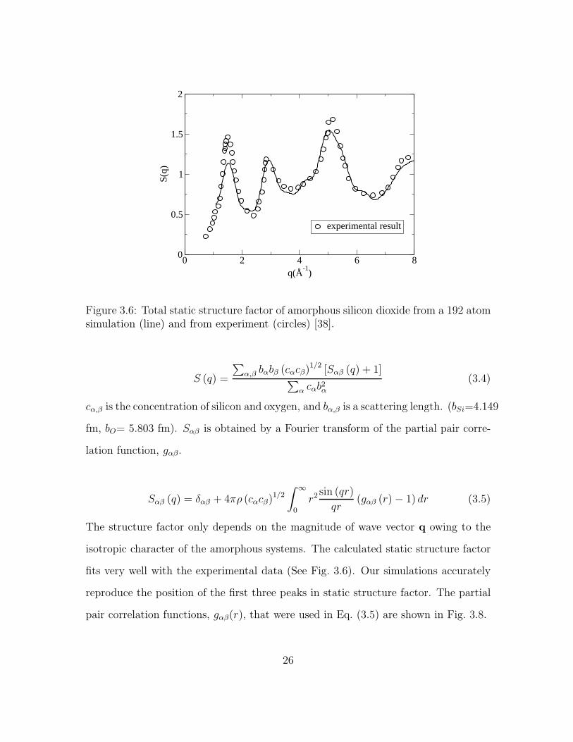
The total static structure factor of neutron scattering experiment is available
for a-SiO2 [37]. Since silica is a heterogeneous system, the structure factor can be
calculated by weighted sum of partial structure factors, Sαβ.
23

Figure 3.4: Concentration of Si and O atom as a function of distance from atomcenter. Our results are compared with the Car-Parrinello MD (CPMD) simulations.
24

Table 3.2: Diffusion constants at several temperatures.
temperature DSi(cm2/s) DO(cm2/s) DSi/DO
ab initio MDPARSEC
3120K 6.7×10⁻⁶ 7.9×10⁻⁶ 0.853700K 1.0×10⁻⁵ 1.5×10⁻⁵ 0.67
CPMD [23] 3500K 5±1×10⁻⁶ 9±1×10⁻⁶ 0.56
classical MDBKS
[35] 3000K 9.5×10⁻⁷ 1.9×10⁻⁶ 0.503580K 1.8×10⁻⁵ 2.8×10⁻⁵ 0.64
CHIK[35] 3000K 4.6×10⁻⁶ 6.6×10⁻⁶ 0.72
3580K 6.0×10⁻⁵ 8.3×10⁻⁵ 0.72
CPMD: Car-Parrinello molecular dynamicsBKS: Beest-Kramer-Santen potentialCHIK: Carre-Horbach-Ispas-Kob potential
Figure 3.5: The circles indicate this work, triangles are CPMD [23], diamonds areclassical CHIK potential [35], and squares are classical BKS potential [35].
25
0 2 4 6 8q(Å
-1)
0
0.5
1
1.5
2
S(q
)
experimental result
Figure 3.6: Total static structure factor of amorphous silicon dioxide from a 192 atomsimulation (line) and from experiment (circles) [38].
S (q) =
∑
α,β bαbβ (cαcβ)1/2 [Sαβ (q) + 1]∑
α cαb2α
(3.4)
cα,β is the concentration of silicon and oxygen, and bα,β is a scattering length. (bSi=4.149
fm, bO= 5.803 fm). Sαβ is obtained by a Fourier transform of the partial pair corre-
lation function, gαβ.
Sαβ (q) = δαβ + 4πρ (cαcβ)1/2
∫ ∞
0
r2 sin (qr)
qr(gαβ (r) − 1) dr (3.5)
The structure factor only depends on the magnitude of wave vector q owing to the
isotropic character of the amorphous systems. The calculated static structure factor
fits very well with the experimental data (See Fig. 3.6). Our simulations accurately
reproduce the position of the first three peaks in static structure factor. The partial
pair correlation functions, gαβ(r), that were used in Eq. (3.5) are shown in Fig. 3.8.
26

Table 3.3: Average bond lengths and bond angles of a-SiO2. Our work is comparedto CPMD, empirical potential MD (EPMD) and experiments. Full width at halfmaximum is indicated in parenthesis.
This work CPMD [24] EPMD [34] EXP [37, 39, 40, 41]
d(Si-O) 1.63 1.62 1.61 1.610(0.09) (0.08) (0.08) ±0.050
d(Si-Si) 3.01 2.98 3.07 3.080(0.36) (0.25) (0.21) ±0.100
d(O-O) 2.67 2.68 2.76 2.632(0.26) (0.21) (0.25) ±0.089
Si-O-Si 138 136 148 140-150(24) ±14 (27)
O-Si-O 110 109 109 109.4-109.7(10) ±6 (15) (15)
We calculated the average values of the bond angle and the bond length in
Table 3.3. For comparison, Car-Parrinello MD and classical MD simulation results
are also tabulated. Our simulation shows good agreement with the experimental
data. Details of the short-range bond angle distributions, Si-O-Si and O-Si-O, are
shown in Fig. 3.7. Previous CPMD results are indicated by a dashed line in the
same figure. A noticeable difference between two simulations is a peak below 100◦
in the Si-O-Si bond angle distribution function. This peak suggests the existence
of two-membered (2m) ring (an edge-sharing pair) as we noted in discussing our
liquid simulations. The relatively small Si-O-Si angle comes from the geometry of
a quadrangular configuration of the 2m ring as shown in Fig. 3.10. This peak also
contributes to a slightly smaller value for average bond angle of Si-O-Si relative to
the experiments in Table 3.3, since even a single occurance of a 2m ring makes a
considerable change the bond angle distribution function owing to the size of the
supercell. The character of 2m ring structure is also detected in partial pair correlation
function in Fig. 3.8. We note the small peak in gSiSi(r) around 2.4 A, which is not
27

60 90 120 150 180
Si-O
-Si
60 90 120 150 180angle (degrees)
O-S
i-O
Figure 3.7: Bond angle distribution function in amorphous silicon dioxide.
shown in the compared CPMD data. Typically, the distances between Si-Si of 2m
rings is in the range of 2.3–2.5 A, which is comparable value to the small peak in
gSiSi(r) figure.
3.6 Defect structure analysis
Two-membered rings have been observed in some previous simulations [26, 28];
however, these rings are absent in other simulations [23, 34]. To understand the
origin of these differences, we performed a variety of different preparations for our
simulations, i.e., we examined cells containing 8, 32, and 64 unit of SiO2 with cooling
28
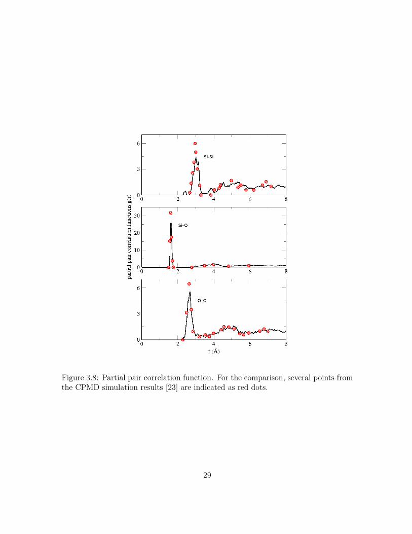
Figure 3.8: Partial pair correlation function. For the comparison, several points fromthe CPMD simulation results [23] are indicated as red dots.
29

0 0.2 0.4Relative Energy (eV/atom)
00.20.40.60.8
11.21.41.61.8
22.22.42.62.8
33.2 2-membered ring
without 2-membered ring
Figure 3.9: Relaxed structure total energy. This graph shows the strain energy oftwo-membered rings do not affect to the total energy of the system.
rates ranging from 2.5 × 10¹⁴ to 1015K/s. Among them, only the simulation for
the 8 units of SiO2 with a cooling rate of 2.5 × 10¹⁴K/s did not result in a 2m ring
configuration. In general, increasing the size of the system allowed the two membered
ring configuration even for the slowest cooling rate.
The same phenomenon was reported by Binder et al. [28] They tested several
cooling rates with 1,002 atoms and the slowest cooling rate was 4.4×10¹²K/s, which is
two orders of magnitude slower than most ab initio simulations. Their study showed
evidence for a 2m ring even for the slowest cooling rate.
In order to determine the possibility of existence of 2m ring in amorphous
structures, we compared total energy of thirteen different systems prepared as men-
tioned above. We picked one snapshot in each simulation at 300 K and performed
structural relaxation for each cell. Among them, we chose the lowest energy as the
zero reference energy. We indicated total energy per atom instead of total energy
since cells contain different number of atoms. The energy differences are not signifi-
cant between the two simulation groups as illustrated in Fig. 3.9.
However, since the 2m ring population is a small fraction of the entire system,
30

Figure 3.10: Clusters used to calculate cohesive energy. (a) corner-sharing cluster.(b) two-membered ring cluster.
total energy comparisons may not accurately reflect the presence of 2m rings. Rather
than performing total energy comparison of the entire cell, we attempted to exam-
ine the energy of the local structure. Extracting an energy representing a localized
configuration is not a trivial exercise within density functional theory as contrasted
with a classical simulation. We estimated the energy cost for a 2m ring and corner-
sharing (see Fig. 3.10) by considering clusters of bulk amorphous silica. Hydrogen
was used to passivate our model clusters. We considered small clusters as it is shown
in Fig. 3.10 and calculated the cohesive energy of two configurations labeled by (a) for
a corner sharing geometry and (b) for a two membered ring cluster. In (a) clusters,
the average value of cohesive energy was -6.17 eV/atom while for (b) clusters was
-6.43 eV/atom, implying the 2m ring clusters are favorable structures compared to
the corner-sharing clusters. To check the applicability of this approach to a bulk envi-
ronment, we considered clusters with a second-shell of SiO2 (Fig. 3.11). The cohesive
energies of both (a) and (b) cluster in Fig. 3.11 were similar, that is -6.56 eV/atom
for (a) and -6.52 eV/atom for (b). Adding second-shell atoms to the cluster results in
reducing the energy difference. This explains why Fig. 3.9 does not show a difference
in total energy between two groups and suggests that there is not a significant energy
disadvantage of generating 2m rings in amorphous silica.
31

Figure 3.11: One more layered cluster of Fig. 3.10 (a) corner-sharing cluster. (b)two-membered ring cluster.
One can argue that a 2m ring may result in a large strain than larger rings,
e.g., three-membered or four-membered ring. However, previously performed sim-
ulations reported the calculated strain energies of 2m ring were in range of 1.23–
1.85 eV/Si2O4 [42, 43, 44] which is smaller than formation energy of oxygen vacan-
cies frequently observed in silica. Boureau et al. [45] discussed the thermodynamical
lower bound of formation energy of the oxygen vacancy in β-cristobalite SiO2 is 7.3
eV/defect and ab initio studies showed the defect formation energy is between 5–9
eV per a defect [46, 47, 34]. These values support the idea that the strain energy of
2m ring may not be a considerable barrier of generating this configuration in silica if
one compares to the oxygen defects.
The formation of the 2m ring on silica surfaces has been also discussed in the
previous infrared studies [48, 49, 50]. In order to understand the vibrational spectrum
of the 2m ring, we calculated the vibrational density of states with the 24-atom
system. Figure 3.12 shows our calculations in comparison to the CPMD simulation
(dashed line) and experiment (circles). The overall agreement with experiment is
good despite the small simulation cell. The dotted line indicates the contribution
32

0 200 400 600 800 1000 1200 1400wavenumber(1/cm)
0
0.05
0.1
0.15
0.2
0.25
VD
OS
Figure 3.12: The calculated vibrational density of states (solid line) and the con-tribution of the four atoms which constitute the two-membered ring (dotted line).32cm−1 was chosen for the gaussian broadening. For the comparison, experimentaldata (circles) and CPMD simulation data (dashed line) were taken from Carpenterand Price [51], and Pasquarello and Car [52], respectively.
of the 2m ring atoms which is extended in 200–1000 cm−1 range. Two distinctive
and broad peaks between 250–450 and 700–900 cm−1 result from the 2m ring, and
the position of these two peaks are similar to the previous theoretical calculations
by Bendale and Hench [48], who showed several sharp peaks between 200–400 and
740–1100 cm−1. In IR experiments on dehydroxylated a-SiO2 surface, two unique
peaks at 888 and 908 cm−1 have been reported [49]. These two peaks are regarded
to be a strained defect, i.e., the edge-sharing structure on the surface. We note that
the IR experiments focused on the surface that was thermally treated. Therefore, the
population of the edge-sharing structure on the surface may have been very dense.
Since the 2m ring is not predicted to be abundant in bulk a-SiO2, we do not expect
contributions from 2m rings to result in vibrational features such as the D1 and D2
defect bands in Raman spectrum, which have been shown to be correlated with a
breathing mode of the 4m ring and 3m ring structure, respectively.
The density of states (DOS) for our simulated amorphous silica is given in
33

-20 -10 0 10energy (eV)
0
1
2
DO
S (
stat
es/e
V)
PARSECEXPCPMD
Figure 3.13: Density of states of amorphous structure. The X-ray photoemissionspectrum data are from Ref. [55].
Fig. 3.13. The dashed-line comes from x-ray photoemission experiments [53]. Each
peak of the DOS can be characterized by the atomic nature of the corresponding
electronic states in the energy region of interest [54, 55]. The states above -5 eV
correspond to lone pair, nonbonding 2p orbitals of O and the energies from -6 to
-11 eV is strong bonding of Si sp3 hybrid orbital and O p orbital. The states in the
region -15 to -20 eV are primarily O 2s orbitals. While the DOS ranging from -5–
0 eV is accurately predicted by our simulation, there is a disagreement around -10 eV
peak between calculated DOS and X-ray photoemission spectra (XPS). According
to Pantelides et al., the disagreement between XPS and the theoretical prediction
is casued by a matrix element effects since XPS is determined by not only valence
electron density of states, but also interaction between bond orbitals at different bond
sites [56]. Owing to this effect, we observed the same disagreement near -10 eV peak
in previous studies [55, 23].
3.7 Summary
In summary, we have performed ab initio molecular dynamics simulations for
both liquid and amorphous silicon dioxide including 64 units of SiO2 using real-
34

space pseudopotentials. In liquid simulations, we considered liquid systems at two
temperatures: 3,120 K and 3,700 K. We showed structural properties and dynamical
properties at each temperature, and compared our work with previously performed
Car-Parinello and classical MD simulations.
We also simulated amorphous silica. We compared several structural prop-
erties to experiments and other previous simulation results. Our calculated static
structure factor reproduced the experimental data very accurately. Bond length and
angle show similar values with comparing data except bond angle distribution. The
differences in Si-O-Si bond angle distributions between previous work and our work
are caused by a two-membered ring structure. We showed the possibility of their
existence in amorphous structure not only by performing cohesive energy calculation,
but also by calculating vibrational spectrum of the two-membered ring. Finally, we
presented the electronic structure of amorphous silica and the results were similar to
the previously performed simulation.
35
Chapter 4
Electronic and structural properties of
nanocrystals and clusters
Nanoscience and nanotechnology are among the most actively developing areas
in material sciences and engineering. Owing to their novel physical and chemical be-
havior, nanoscale materials have been designed applications in energy conversion and
storage, laser, bio-sensing, and catalysis [57, 58, 59]. Nanostructures, e.g., nanocrys-
tals, nanowires, and nanoclusters, are spatially confined in at least one direction
within a range of 1–100 nm. This results in “quantum confinement”, which alters
the electronic and optical properties of nano-scale materials compared to their bulk
counterpart [60]. To investigate nano-scale systems, quantum-mechanical based com-
putational studies are necessary. Such studies increase the level of understanding
of these materials and provides insights on how to design efficiently new materials
for industrial applications. In this chapter, we study metal oxide nanomaterials to
illustrate how electronic structure calculations can aid in understanding electronic,
structural, and optical properties of nanostructured materials. Specifically, results
are presented for SnO2 and TiO2.
4.1 SnO2 nanocrystals
4.1.1 Introduction
Transparent conducting oxides (TCOs) exhibit very interesting properties as
they are optically transparent in visible light, but electronically conductive. Owing to
36

their broad industrial applications such as optoelectronic devices and photovoltaics,
there has been much attention for TCO materials [61]. The most widely used TCO
material is In-doped tin oxide (ITO), yet In is not abundant in nature. Sb- or F-doped
tin oxide is considered to be a good alternative to ITO [62].
Although thin films are a widely used form for this material, more interesting
phenomena have been observed for nanocrystals. Successful synthesis of Sb- and F-
doped nanocrystals with a size of less than 10 nm diameter have been reported [63,
64, 65]. This broadens the opportunity to use these nanocrystals to manufacture
thin films or other nanostrucutres [66, 67]. For nanocrystals in general, controlling
electronic properties depends on not only the impurity, but also the size and the
shape of nanocrystals. Computational study plays a crucial role in providing detailed
information about these relationships. However, there are very few computational
studies reported [68] because of the complexity of the rutile structure, which is the
most stable crystal form of SnO2.
In this section, we present electronic structure calculations of Sb- and F-doped
SnO2 nanocrystals. Formation energy and electron binding energy, calculated by the
total energy difference of neutral and charged particles, for Sb and F dopants are
discussed. Our results show strong quantum confinement effects not only in the
homo-lumo1 gap of pure nanocrystals, but also in the electron binding energy of
doped nanocrystals, which is consistent with the previous nanocrystal studies [69, 70].
We also illustrate differences in structural and electronic properties between Sb- and
F-doped tin oxide nanocrystals.
1homo and lumo stand for highest occupied molecular orbital and lowest unoccupied molecularorbital, respectively
37

4.1.2 Computational details
All calculations are based on density functional theory utilizing real-space
pseudopotentials. Convergence is determined by a grid spacing, which is 0.3 a.u.
in these calculations. With this grid spacing, the total energy converges within
0.01 eV/atom. To find a minimum energy structure of each nanocrystal, we used
the BFGS method2 and all atoms were allowed to move until the largest force is less
than 0.005 Ry/a.u. The domain size was chosen to be 6.5 a.u. larger than the outer-
most atom of the nanocrystal. Outside of this spherical domain, the wave function is
set to be zero.
The pseudopotentials for Sn and O were generated with a valence configuration
of 5s25p2 and 2s22p4, respectively. We did not include 4d electrons in the valence
configuration, i.e., it is frozen into the core states, as the 4d states of Sn does not
affect the shape of the band structure except very deep levels [71]. We employed
the local density approximation (LDA) for the exchange-correlation functional from
Ceperley and Alder [5]. With these pseudopotentials, we obtained a band gap of
1.02 eV and the band structure is shown in Fig. 4.1. The experimental band gap
for rutile SnO2 is 3.6 eV which is much larger than our LDA band gap. It is a well-
known fact that the LDA underestimates the band gap. Since we are interested in
changes in the electronic structure, exact band gap calculations are not necessary for
the purposes of our study.
To construct our model for nanocrystals, we started with the rutile crystalline
SnO2 structure. We set the center atom to be Sn, then selected atoms that reside
inside a sphere with a given radius. Sn atoms with more than two dangling bonds
2Named after its inventors: Broyden, Fletcher, Goldfarb and Shanno.
38

Figure 4.1: Band structure of bulk SnO2. A direct band gap of 1.02 eV is observed.
39

Table 4.1: The number of atoms and diameter of the nanocrystal.
D(nm) Sn O H Total1.27 29 60 70 1591.69 69 140 138 3471.97 111 220 166 4972.37 191 384 262 837
and O atoms with more than one dangling bond were removed. To passivate dangling
bonds on the surface atoms, we generated fictitious hydrogens with fractional nuclear
charges and electrons. Sn and O dangling bonds were passivated with fiticious hy-
drogen atoms with 43
and 23
fractional charge, respectively [68]. In this way, we were
able to keep the same electron configuration of the rutile structure for the surface
atoms. Several sizes of nanocrystals were constructed with a diameter from 1.2 nm
to 2.5 nm. The diameter was defined by the expression d = (Ntot×Vunitcellπ )3. The
number of atoms in each nanocrystal is indicated in Table 4.1, and the shape of the
nanocrystals are shown in Fig. 4.2.
4.1.3 Results and discussion
4.1.3.1 Quantum confinement effect in Sb-doped SnO2 nanocrystals
In doped nanocrystals, the energy gap and binding energy can depend on the
size of the nanocrystals. It is a well-known fact that a strong blue shift occurs to the
energy gap as the dimension of the nanocrystals approaches the exciton bohr radius
(aB) due to the quantum confinement. Below aB, the electron and hole motion is
not treated as a correlated pair [72]. To investigate the size effect on the electronic
properties of the pure SnO2 nanocrystals, we calculated fundamental gap, defined as:
Eg = IP − EA (4.1)
40

Figure 4.2: Structure of H-passivated SnO2 nanocrystals. Sizes of the nanocrystalsare: (a) 1.27 nm, (b) 1.69 nm, (c) 1.97 nm, and (d) 2.37 nm.
where IP and EA are the ionization potential and the electron affinity, respectively.
IP and EA are calculated by the total energy difference between charged and neutral
system, defined by:
IP = E(n− 1) − E(n)
AE = E(n) − E(n+ 1).(4.2)
n indicates the number of the total electrons of the neutral system. Within the real-
space formalism, IP and EA calculations are straightfoward for the confined system
as it does not require an artificial periodicity. To calculate the energy of the charged
system in periodic boundary conditions, a mathematical trick, such as an artificial
jellium background [73], should be considered to prevent the Coulomb energy from
diverging. Figure 4.3 shows the energy gap for the undoped nanocrystals (black
diamonds). Since the exciton bohr radius for SnO2 is 2.7 nm [74], which is larger
than all of our nanocrystal sizes, we observe very steep increase in the energy gap as
41

1 1.5 2 2.5diameter (nm)
0
1
2
3
4
5
6
eV
Egap
Ebind
Figure 4.3: Fundamental gap of the pure SnO2 nanocrystals (black diamonds) andelectron binding energy of the Sb-doped nanocrystals (red diamonds).
the size of the nanocrystal decreases.
Electron binding energy is one of the key properties of doped semiconductors.
As Sb has one more valence electron than Sn, the extra electron creates a donor state,
n-type doping. In the n-type bulk semiconductor, the binding energy is defined as a
difference between the minimum conduction band energy and the donor state energy.
In a confined system, a more appropriate definition for the binding energy would
be the difference between the ionization potential of the doped nanocrystal and the
electron affinity of the pure nanocrystal [69]:
EB = IPd − AEp (4.3)
where d and p indicate doped and pure state, respectively. IPd, EAp, and EB values
with respect to the size of the nanocrystal are illustrated in Fig. 4.4. We note that
the Sb atom is located at the center of the nanocrystal. One interesting aspect of
this figure is that IPd does not change with respect to the size of the nanocrystal,
whereas the EAp has a strong size dependence. This is due to the localized donor
state as shown in the Fig. 4.6. The energy required to detach the defect electron from
42

1 1.5 2 2.5Diameter (nm)
0
1
2
3
4
5
6
eV
IPd
EAp
Ebind
Figure 4.4: Ionization potential of the doped nanocrystal (blue) and electron affinityof the pure nanocrystal (red).
the nanocrystal remains the same level regardless of the size of the nanocrystal. This
“pinned” energy level was also reported in previous nanocrystal studies for n-type
dopant systems [70].
Formation energy can be a measure of the stability of the doped nanocrystal.
It has been reported that a smaller nanocrystal tends to possess higher formation
energies [75, 76]. To determine if this is a case for SnO2 nanocrystal as well, we
calculated the formation energy of the Sb atom. In bulk systems, formation energy
depends on the chemical potential that is related to the partial pressure of the gas,
and the Fermi level. As we focus on the neutral defect in this study, the Fermi energy
is not taken into account in our analysis [75]. Therefore, the formation energy is
written:
Eform = Etot(Sb:SnO2) − Etot(SnO2) + n[µ(Sn) − µ(Sb)] (4.4)
where n is the number of defect atom of the particle and µ is the chemical potential.
Although µ is related to the different thermodynamic limits [77], we consider the
chemical potential to be the energy of the individual atom obtained from the bulk
43

crystaline structure for both Sn and Sb atom. Figure 4.5 shows a relative formation
energy of the nanocrystal. In general, more positive formation energy means less
favorable, indicating that the smaller nanocrystal requires more energy to dope the
Sb atom into the nanocrystal. To understand this phenoenon, we plot the isosurface of
the defect level orbital in Fig. 4.6. The same value of the electron density was chosen
for both isosurface plots. In small nanocrystals, the electrons are more localized
around the Sb atom. This may increase the kinetic energy of the electron, which
adds the energetically unstable character to the doped nanocrystal.
4.1.3.2 Antimony vs. Fluorine dopant atoms
As mentioned earlier, F is also used as n-type dopant for SnO2. The F-doped
SnO2 nanocrystals have been synthesized within a range of 3–10 nm by means of the
chemical vapor synthesis [64]. Owing to the smaller size of F compared to Sb, two
possibilities for the doping site can be considered, i.e., substitutional and interstitial
doping sites. Experimental studies of F:SnO2 nanocrystals show that at low F concen-
tration, F substitutes O. For high F concentration, interstitially doped F is observed,
but they tend to make substitutional-interstitial pair [64]. In this study, we consider
only one F atom in the nanocrystal, which is considered low doping concentration, to
compare the difference between Sb and F. We constructed F-doped nanocrystals that
substitute F for O. We chose the same nanocrystal size of 1.69 nm for both Sb and F
doped nanocrystals, and located Sb at the center and F at the nearest neighbor from
the center Sn atom as the size of the nanocrystal is relatively small.
Figure 4.7 shows the visualized defect state wave function for Sb (left) and
F (right). The defect state of the Sb dopant is localized on the Sb atom. For the
F-doped nanocrystal, however, the defect wave functions are lying between F and
44

1 1.5 2 2.5Diameter (nm)
-3
-2
-1
0E
form
(eV
)
Figure 4.5: Formation energy for the antimony dopant atom with respect to the sizeof the nanocrystal.
Figure 4.6: Dopant level wave function isosurface plot. Red and purple indicateoxygen and tin, respectively. Blue sphere indicates the surface hydrogen. Wavefunction is localized around the dopant antimony atom.
45

Figure 4.7: Defect wave function isosurface plot. Antimony and fluorine dopants areindicated in grey and yellow color, respectively.
Sn. This hybridized orbital feature is also observed in the bulk F:SnO2 system.
Velikokhatnyi and Kumta performed DFT calculations for Sn16O31F, and presented
total and projected density of states [78]. Rather than creating new states below the
conduction level, F-doping causes a Fermi-level shift towards to the conduction level.
Accordingly, additional electrons by F doping exhibit 5s and 5p Sb character rather
than 2p F character, which is similar to our observation.
To compare the structural difference in Sb and F doping, we calculated average
bond length changes in Sb-O and Sn-F compared to original Sn-O bond length, and
their changes was found to be small. However, the opposite trend between Sb and
F in bond length changes were observed. For the Sb doping, the Sb-O bond length
shrinks about 0.05 A which is a 2.5% decrease compared to the original Sn-O bond
length. On the other hand, the Sn-F bond increases by 0.15 A. This opposite trend
can be understood by calculating fractional charge on each atom. As Sn and O atom
have six and three bonds respectively, Sn provides −23
to O to make +4 ionic charge
because the electronegativity of O is larger than Sn. When we substitue O with F,
only one electron can fill the empty 2p state of F. Once the F 2p orbitals are filled,
46

remaining electrons act to fill 5s and 5p states of Sn rather than the 3s state of F.
This may cause the defect electron density splitting that we found in Fig. 4.7, and
the stretched bond length. The electron binding energy for Sb and F doping was
calculated as well, and their values are 2 eV and 2.8 eV, respectively. From this
result, we expect that F doping creates a deeper donor state than Sn doping.
4.1.3.3 Higher doping concentration
In the previous sections, we have considered the effect of Sb and F doping
in SnO2 nanocrystals for only one dopant in each nanocrystal. Several experimental
studies have reported that highly doped Sb:SnO2 materials exist in both thin films
and nanocrystals [79, 80]. A 2–7% doping concentration for Sb is known to produce
a degenerate semiconductor, which has a high electrical conductivity. In order to
investigate the effect of different doping concentrations on the electronic structure of
small nanocrystals, we considered four different doping concentrations (0.3, 1.2, 2.7,
and 3.9 at%) with a nanocrystal of a 1.97 nm diameter. For each concentration, we
substituted Sn to Sb and the dopant atoms were not very close to each other.
Figure 4.8 shows the binding and formation energy of the Sb dopant. Both
binding and formation energies decrease as the concentration of the antimony dopant
(cSb) increases. Our results indicate that the higher dopant concentration is more
energetically favorable than the lower concentration. This trend is oppostie compared
to ZnO nanocrystal calculations [81]. In ZnO nanocrystals, we tried substitutional
doping for Zn to Ga, and more than two Ga atoms showed much higher formation
energy than one Ga atom. It explains that why one can observe high Sb concentrations
in Sb:SnO2 system. For binding energies, as the electron affinity does not change in
Eq. 4.3, IPd decreases as a function of the cSb. This indicates that high doping
47

0 1 2 3 4Sb concentration (at%)
-4
-2
0
2
Ene
rgy
(eV
)
Ebind
Eform
Figure 4.8: Electron binding energy (diamond) and formation energy (square) fordifferent doping concentration.
concentration changes the dopant level character from deep to shallow, which makes
these particles more attractive in the applications for electric devices.
4.1.4 Summary
In summary, we presented electronic structures for SnO2 nanocrystals within
a range of 1.3–2.4 nm diameter. Strong quantum confinement effect was observed not
only for the pure nanocrystals, but also for the Sb-doped nanocrystals. The binding
energy of the Sb dopant showed a strong confinement due to the highly localized
nature of the dopant wave function. We also examined the differences in dopant level
between Sb- and F-doped nanocrystals. The higher concentration of Sb was revealed
to lower the nanocrystals’ formation energy and binding energy as well.
4.2 TiO2 clusters
4.2.1 Introduction
TiO2 is one of the most studied transition metal oxides owing to its high
potential in many industrial applications. Specifically, photocatalytic activity of TiO2
48

has attracted much interest [82] to meet demands for clean energy production. In
particular, small TiO2 clusters, containing up to a couple of tens of atoms, exhibit
exciting properties as they alter the optical properties [83]. To make this material
more attractive in such applications, it is essential to understand their electronic and
structural properties; however, due to a small dimension, there is no definitive way
to characterize the relationship between the electronic properties and their geometry.
Computational study combined with the global minimum (GM) search have been
conducted based on a conventional belief that the GM structure would be the most
probable structure in nature. Nevertheless, no such agreement with photoemission
spectroscopy (PES) has been achieved [84].
In this section, we present methods for determining the low energy structures,
and introduce many-body theory calculations that are beyond the Kohn-Sham one-
electron interpretation in order to acquire better optical properties.
4.2.2 Global minimum searching methods
4.2.2.1 Simulated-annealing technique
Simulated-annealing is a method for solving the global optimization problem.
Previous theoretical studies on clusters have shown that this method is an effective
way to determine the structures of small size clusters [31]. In our calculations, the
simulated-annealing technique was performed in two steps:
1) Molecular dynamics simulation:
We generated random configurations of titania clusters. Each (TiO2)n system was
coupled with a heat bath and the temperature was controlled via Langevin dynamics.3
3The details of Langevin dynamics were explained in chapter 3.
49

Figure 4.9: Annealing schedule. The initial temperature was set to 3000K and thetemperature was decreased at every 100 steps until when temperature reaches to300K. For (TiO2)4 cluster simulations, we chose the temperature step of 250K insteadof 500K.
Initial and final temperature and the details of annealing schedules are shown in
Fig. 4.9. A time step of 200 a.u. and a friction coefficient of 0.0005 a.u. were chosen
to integrate the equation of motion. The grid spacing and the boundary sphere radius
were 0.35 a.u. and 20 a.u., respectively.
2) Structural relaxation:
The structure of each cluster obtained from MD simulations was relaxed until the
maximum force component is less than 0.004 Ry/a.u. This was performed with a
finer grid spacing of 0.20 a.u. to ensure accurate forces. The boundary sphere radius
was chosen such that the distance between the outermost atom and boundary was
larger than 8 a.u.
4.2.2.2 First-principles basin-hopping technique
Basin-hopping is a Monte-Carlo based method for exploring potential energy
surfaces (PES) by performing consecutive jumps from one local minimum to another.
As shown in Fig. 4.13, this method provides transformed PES that maps each config-
uration space to one local minimum energy. To perform basin-hopping optimization,
50

Figure 4.10: Illustration of basin-hopping optimization process. E({Rm}) respresentsthe original potential-energy surface and E ({Rm}) is transformed potential-energysurface. Adapted from Ref. [85].
the initial random cluster is generated and the configuration of the cluster is modi-
fied by a set of trial moves (∆Rm = rme(θ, φ), where e(θ, φ) is a random unit vector
expressed in spherical coordinates and rm is a move distance for atom m. Rm is the
position of atom m) created by uniformly distributed random numbers, followed by
a local relaxation [85]. A trial move and a relaxation are indicated as green and red
arrows in Fig. 4.13. This method has been successfully applied to Lennard-Jones clus-
ters and biomolecules, but for small clusters of our interest, PES should be considered
within a quantum mechanical way. In this study, the basin-hopping optimization was
performed based on DFT with Perdew-Burke-Ernzerhof (PBE) exchange-correlation
functional [86].
The comparison between simulated-annealing and basin-hopping is shown in Fig. 4.11
and Fig. 4.12. The most stable structures and their relative energies are indicated.
The results of simulated-annealing and basin-hopping are consistent. The energy
differences between the global minimum cluster to other isomers of two simulations
agree within 0.4 eV.
51

Figure 4.11: n=2-3 isomers
52

Figure 4.12: n=4 isomers
4.2.3 Computational details
All electronic structure calculations were performed by using the all-electron
numerical atom-centered orbitals code fhi-aims [87]. The numerically tabulated
atom-centered orbital basis sets are grouped into a minimal basis, containing only
basis functions for the core and valence electrons of the free atom, followed by four
hierarchically constructed tiers of additional basis functions (tiers 1–4) [88]. For the
global minimum search, we used both simulated-annealing performed by the parsec
code, and basin-hopping with a tier 1 basis set. Up to n=4 (TiO2)n clusters, the same
global minimum structures were obtained from both methods. However, the basin-
hopping method provided a wider spectrum of isomers that enabled us to compare our
53

clusters to the experiment. We used basin-hopping for bigger clusters, and examined
all isomers found within 1.25 eV from the global minimum energy.
It is essential to calculate accurate values for homo-lumo energy to make a
direct comparison with electron affinity and detachment energy observed in experi-
ment. To do this, we performed many-body electronic structure calculations within
the GW method, where G is the one-particle Green’s function and W is the dynam-
ically screened Coulomb potential [89, 90]. To mitigate the computational demand,
we used a perturbation approach denoted by G0W0. Within G0W0 calculations, G
and W are obtained by the first-order corrections to the DFT eigenvalues. Our G0W0
results are based on PBE-based hybrid functional [91].
4.2.4 Structural analysis of the low-energy clusters found in basin-hopping
One might expect that the experimentally observed structure to be a global
minimum structure. Interestingly enough, this energy-structure analogy does not
apply to all of the TiO2 clusters. In Fig. 4.13, we present the lumo level of neu-
tral clusters and the homo level of anion clusters to compare to the experimentally
observed electron affinity (EA) and vertical detachment energy (VDE). Global mini-
mum isomers, expected to be the case for the best agreed structure, are illustrated as
red triangles. However, global minimum isomers do not match with either EAs and
VDEs. The best agreement is observed with highest vertical electron affinity (VEA)
clusters, i.e., the isomer that holds the lowest homo energy, except n=4 and 5. For
these clusters, slightly lower VDE isomers were selected to be a better agreement
with both EA and VDE. These clusters are indicated as green diamonds.
Highest VDE isomers also present highest VEA except n=4, 5, and 7. To
investigate the correlation between highest VEA and the structures, we performed
54

Figure 4.13: lumo energies for neutral clusters (upper), and homo energies for anionclusters (lower). Courtesy of Noa Marom.
structural analysis and found that the highest VEA clusters have three things in
common, except for the n=7 cluster:
a. The highest VEA clusters have only one tri-coordinated Ti atom, on
which the anion homo orbital is localized.
b. The oxygen atoms bound to the tri-coordinated Ti atom do not have
a dangling bond.
c. The bond angle of O-Ti-O is close to the tetrahedral angle of 109.5 ◦.
The structures that hold those three properties are shown in Fig. 4.14 and Fig. 4.15.
We listed clusters whose root-mean-square deviation is less than 10 ◦ from the tetra-
hedral angle for n ≥ 5 clusters. (For n < 5 clusters, root-mean-square deviation
becomes larger compared to the bigger clusters.) All tri-coordinated Ti atoms are
shown as green spheres. The anion homo is highly localized on that Ti atom.
55

Figure 4.14: Structural analysis for the cluster size of n=2-6.
56

Figure 4.15: Structural analysis for the cluster size of n=7-10.
57

Can one explain why the photoemission spectroscopy (PES) selectively ob-
serves the high VEA isomers rather than the global minimum structures? These
couterintuitive results were also observed in the study of SiD− clusters [92]. To an-
swer this question about the higest VEA observation, Kronik and coworkers assumed
that the neutral low energy isomers can be generated with equal probability due to
the high temperature [92]. When the clusters enter the plasma region, electrons are
selectively attached to the high VEA, in which the cluster includes Ti3+ site in our
case. After transforming to the anion, they may have a dwell-time before measure-
ment, then the clusters can relax to the metastable structure. Before these isomers
transfer to more stable structure, PES mesurement is performed. This explains how
we obtained the better agreement with the high VEA isomers, not the global mini-
mum structures.
4.2.5 Summary
We studied (TiO2)2−10 clusters by means of DFT-based basin-hopping and
simulated-annealing for the global minimum search, and the many-body perturba-
tion theory within G0W0 approximations for the electronic structure calculations.
Our simulations demonstrated the structure-selection criterion in photoemission spec-
troscopy experiments: the high vertical electron affinity clusters are selectively ob-
served rather than the global minimum clusters.
58

Chapter 5
Noncontact atomic force microscopy study
5.1 Introduction
Scanning probe microscopy is a widely used technique in surface science and
nanotechnology for studying surface properties. Since the invention of scanning
tunneling microscopy (STM) in 1982 [93] and atomic force microscopy (AFM) in
1986 [94], scanning probe microscopy has evolved not only to provide a better reso-
lution, but also to be applicable for a wide range of materials.
STM probes tunneling currents between the tip and the sample, which reflect
the distribution of electron states available for electron transfer. In order to measure
the tunneling current, STM requires conducting materials, which limits the use of
STM to various materials. Also, STM cannot be used in ambient conditions without
proper surface preparation. On the other hand, AFM probes forces between the
tip and materials, which do not require electrical conductivity. Consequently, AFM
became a popular probe microscopy.
The basic components of AFM are a light source, a cantilever containing a
sharp tip, a sample surface, and a photodetector as illustrated in Fig. 5.1. A sample
surface is mounted on a piezocrystal, which adjusts the position of the sample and
the probe. Once the position of the tip and the sample are determined, the deflection
of the cantilever is monitored by the change of the path of the laser beam. Since the
deflection is directly affected by tip-sample interactions, the tip geometry is known
59

Figure 5.1: Basic AFM set-up. Adapted from Ref. [95]
to be important for determining the interaction between the tip and the surface.
However, the tip shape dependency can be overcome by the sharpness and the aspect
ratio of the tip [95]. Most commercially manufactured AFM tips have a square-based
pyramid or a cylindrical cone shape.
The primarily AFM operation mode is a simple contact mode [95], which
utilizes the strong repulsive force between the AFM tip and the surface. Even though
the contact mode AFM showed successful images on atomic and molecular scale,
Pethica et al. [96] observed that contact AFM could not observe atomic defects since
the contact area is a limit to AFM resolution.
True atomic resolution has been achieved by noncontact AFM (nc-AFM) [97].
NC-AFM captures weak attractive forces between the tip and the sample rather than
strong forces. In nc-AFM, two operating modes are available: amplitude modula-
tion [98] and frequency modulation [99]. While amplitude-modulated AFM is known
for working well in air and liquid environments, frequency-modulated AFM works
well in ultra-high vacuum conditions, which is used in many traditional surface stud-
ies [99].
60

Even though nc-AFM has been applied to many surface structures, ambigu-
ous results are sometimes reported when the surface contains defects or reconstructed
structures. Consequently, theoretical studies have an important role in a comprehen-
sive analysis of AFM images of materials.
In general, AFM simulations include the AFM tip in order to calculate forces
between the surface and tip apex atom. To calculate the frequency shift of the AFM
tip, the forces over the range of the tip trajectory are integrated. Accordingly, the
tip-surface force must be calculated at every point within the region of interest. This
approach requires a large number of computationally intensive calculations. Another
difficulty comes from the geometry of the AFM tip since the atomic configuration of
the tip is usually unknown.
These difficulties can be overcome considering the fact that AFM images are
not sensitive to the tip. Recently, a possible solution for reducing computational
work was proposed by Chan et al. [100] They showed an effective calculation method
without including an explicit description of the tip. They successfully applied this
scheme to well-known surface structures, such as the Si(111)-(7×7) and TiO2(110)-
(1×1) surfaces. The power of the method by Chan et al. is that it only requires one
self-consistent calculation for a given a model of the surface.
In this chapter, we describe how to investigate complex nanostructured sur-
faces and two dimensional organic molecules by simulating nc-AFM images. Our
study is based on the new method that Chan et al. proposed, but also includes
computations with a physical model of the tip.
61

5.2 Framework for simulating noncontact atomic force mi-croscopy images
AFM responds to atomic forces between the tip and surfaces. As such, un-
derstanding the nature of the atomic force is a key aspect of describing the AFM
operation. Noncontact-AFM measures the change in oscillation amplitude or fre-
quency of the tip that is mainly caused by attractive forces between the tip and the
surface. In this study, we focus on describing frequency-modulated nc-AFM under
ultra-high vacuum conditions.
5.2.1 Forces between the tip and sample
In general, the forces which determine the AFM image can be classified as
long-range forces and short-range forces. Van der Waals, electrostatic and magnetic
forces are considered long-range forces and chemical forces are considered short-range
forces [101].
The van der Waals (vdW) force originates from the dipole fluctuations caused
by the correlated motion of electrons. Electrostatic forces are strong long-range forces
caused by charged objects. Two different sources are responsible for the electrostatic
force, i.e., charged defects and contact potential differences. Charged defects can be
generated during the surface preparation process. However, these charges can often
be removed by heating the sample surface [102]. The contact potential difference
arises from the difference in the work function of two different materials. When two
materials are brought into an electric contact, electrons transport from one material
with a smaller work function to the other with a higher work function until they reach
the same Fermi level. This contact potential difference is a key measurement in Kelvin
probe force microscopy, which is also a widely used scanning force microscopy [103].
62

Figure 5.2: Tip motion in nc-AFM. The equilibrium tip-surface position is at q = 0,and d is the closest distance between the tip and the surface.
In nc-AFM experiments, the contact potential difference can be cancelled out by
applying a bias voltage to the tip.
Short-range chemical forces originate from the interaction of atomic orbitals,
Pauli exclusion principles, and ion-core repulsion. The strong repulsive short-ranged
forces are dominant in contact mode AFM operation.
5.2.2 Derivation of expressions for the frequency shift calculations
Once the type of force is identified, one can set up an equation which governs
the motion of the tip. Generally, the tip motion is assumed to be a one-dimensional
oscillator with an effective mass, m:
mz(t) +mf0
Qz(t) + kz(t) − Fts(zc + z(t)) = Fext(t), (5.1)
where k, Q, and f0 are the spring constant, the quality factor, and the resonance
frequency of the tip, respectively [104]. Fext is the external force which drives the
oscillating motion. Figure 5.2 shows a schematic of the tip motion.
In the frequency-modulation mode, the tip oscillates with the resonance fre-
quency, f0, which is a material-dependent parameter. To keep a constant amplitude,
63
the feedback-loop adjusts the external force to compensate for the damping force,
(mω0/Q)z(t). Then, Eq. (5.1) can be rewritten as
mz(t) + kz(t) − Fts(zc + z(t)) = 0. (5.2)
This equation is normally solved with two approximations:
1) Small oscillating amplitude approximation:
If the tip oscillates with small amplitude, the tip-surface interaction forces can be
described with a first-order Taylor series expansion, Fts(zc +z) ≈ Fts(zc)+z ·∂Fts
∂s|s=zc
.
Eq. (5.2) is now written:
mz(t) +
[
k −∂Fts
∂s
∣
∣
∣
∣
s=zc
]
z(t) = Fts(zc). (5.3)
The solution for the second order differential equation is given by z(t) = A0 cos(2π(f0+
∆f)t) where A0 is the amplitude of the oscillating tip. Then the frequency shift is
approximated by
∆f ≈ −f0
2cz
∂Fts
∂s
∣
∣
∣
∣
s=zc
. (5.4)
2) Large oscillating amplitude approximation:
In most experimental conditions, frequency-modulated AFM uses a relatively large
oscillating amplitude compared to the typical tip-surface interaction distance. In
these conditions, the frequency change can be considered to be a small perturbation.
The general expression for the frequency shift based on Hamilton-Jacobi for-
malism [105, 106] is
∆f = −f0
2kA20
< Ftsz >
= −f 2
0
kA0
∫ 1
f0
0
Fts(d+ A0 −A0 cos(2πf0t)) cos(2πf0t)dt.
(5.5)
64

Substituting q = A0 cos(2πf0t) in Eq. (5.5) yields
∆f =f0
kπA20
∫ A0
−A0
Fts(d+ A0 − q)q
√
A20 − q2
dq. (5.6)
Integration by parts rewrites Eq. (5.6):
∆f = −f0
2k
∫ A0
−A0
kts(d+ A0 − q)2
A20π
√
A20 − q2dq. (5.7)
This equation is similar to Eq. (5.4), where the kts is replaced by a weighted average.
5.2.3 An efficient method for force calculations
There can be different sources causing the frequency shift in noncontact-AFM
experiments. First-principles analyses have been performed to calculate the quantum
chemical force caused by interactions between the tip and the surface. In a previous
first-principles study, Chan et al. [100] suggested an efficient method that does not
include an explicit description of the tip. Their method treats the influence of the
surface on the tip as a small perturbation, assuming that the motion of the cantilever
tip does not affect the electronic states of the surface. Based on this approximation,
the tip-surface interaction energy can be written as
Ets(r) =
∫
|φ(r′ − r)|2Vts(r′)dr′, (5.8)
where r, Vts, and φ are the position of the tip, the potential on the tip generated
by surface atoms, and the electronic state of the tip, respectively. Since force is a
gradient of total energy, the tip-surface force can be described expanding the potential
up to the first-order expansion around tip position r:
65

Fts = −∇Ets(r)
≃ −∇Vts(r) −∇
[
∇Vts(r)
∫
|φ(r′ − r)|2(r′ − r)dr′]
= −∇Vts(r) −∇ [∇Vts(r) · p]
= −∇Vts(r) − α∇(
|∇Vts(r)|2)
,
(5.9)
where p is the polarization of the tip, assumed to have a linear relation to ∇Vts by
α, the polarizability of the tip material. The first term is a monopole caused by the
electrons of the tip, which is canceled by the ionic potential of the tip if the tip is
neutral. In this setting, the force acting on the tip is now proportional to the dipole
interaction,
Fts(r) ∝ −∇(
|∇Vts(r)|2)
. (5.10)
The tip-surface potential is evaluated by the Hartree and the ionic potential from ab
initio calculations: Vts = Vhart + Vion. Note that the exchange-correlation potential is
not included because the tip is not treated as a quantum system.
Here, we calculate the self-consistent potential Vts(r) of the surface and eval-
uate the force using Eq. (5.10). The frequency shift of the tip is calculated with
Eq. (5.4) and (5.7) for a given height and amplitude. The nc-AFM images are gener-
ated by tracing the contour surface of constant ∆f .
The calculated tip-surface force from Eq. (5.9) can be inserted to Eq. (5.6) to
compute the frequency shift. Since Vts decays very fast in vacuum, the most relevant
integration region is only a couple of angstroms near the tip-surface turning point (d
in Fig. 5.2). Therefore, the integration region in Eq. (5.6) can be reduced from (−A0,
A0) to (−A0, −A0+2∆), with ∆ chosen to be small compared to A0.
66

5.3 Two-dimensional structures
5.3.1 GaAs(110) surface
We chose GaAs(110) surface as it is a simple surface on an extensively stud-
ied material. This surface does not reconstruct, but noticeable surface relaxation is
observed wherein the As atom moves out of the surface plane and Ga atom moves
inward. As other III-V(110) and II-VI (110) semiconducting surfaces possess a simi-
lar relaxed morphology, GaAs(110) can be considered as a prototype of these surface
systems.
5.3.1.1 Computational details
All calculations were performed with real-space pseudopotentials with the lo-
cal density approximation for the exchange-correlation functional from Ceperley and
Alder [5]. The convergence of the total energy is controlled by the grid spacing, which
was taken to be 0.35 a.u. We used Troullier-Martins pseudopotentials [7] with a par-
tial nonlinear core-correction for the Ga atom [107]. The parameters used to generate
the pseudopotentials were obtained from a previous work by Kim and Chelikowsky
for vacancies in the GaAs surface [108]. With these pseudopotentials, we obtained a
lattice parameter of 5.59 A, which agrees within 1 % of the experimental value [109].
Our simulation cell for the GaAs(110) surface contains a 1×2 surface unit
with five atomic layers that corresponds to a slab thickness of 17.79 A, and 21 A of a
vacuum was inserted. In order to passivate the dangling bonds on the opposite side
of the surface, we generated hydrogen-like pseudopotentials with a 1s0.75 and 1s1.25
ionic configuration for Ga and As atom, respectively [110]. The ~k-points were gen-
erated by a Monkhorst-Pack scheme [111] with a 4×3 mesh. Geometry optimization
was performed until the force acting on each atom is less than 0.004 Ry/a.u. After
67

Figure 5.3: A side view (a) and a top view (b) of the relaxed GaAs(110) surface.Magenta, yellow, and blue indicate Ga, As, and H, respectively.
structural relaxation, the Ga atom moved inward and the As atom moved outward
with 0.69 A of buckling as illustrated in Fig. 5.3-(a). This value agrees very well with
the observed value of 0.69 A in the experiment [109].
To create the simulated AFM image, we set two parameters in Eq. (5.7): A0
and d. We tested the sensitivity of these parameters to the AFM images by varing the
values for A0 from 5 nm to 50 nm, but have not found significant changes in image
contrast. A0 is chosen to be similar to the typical oscillation amplitude (10 nm) used
in experiment [112]. The integration limit ∆ is selected to be 1 A for all calculations.1
5.3.1.2 Results and discussion
The parameter that has the most significant effect on the AFM image is the tip
turning point d. Figure 5.4 shows our simulation images with three different values
for d: 3 A, 4 A, and 5 A for (a), (b), and (c), respectively. In this figure, we observe
the opposite trend of how the Ga and As atoms respond. As the tip turning point
1We also tested the effect of the value for ∆ by chaning it from 0.5 A to 2.5 A, but no contrastchange was observed.
68

increases, the bright spots which correspond to the Ga atom disappear while the As
atom becomes bigger and brighter. Typically, most AFM experiments on III-V(110)
semiconducting surfaces have shown only the anion image which is similar to Fig. 5.4-
(c). This seems natural because the III-V(110) surface has a surface buckling, i.e.,
the anion is displaced to the vacuum. However, some recent experimental studies
have reported simultaneous observation of both the anion and cation sublattices. In
the case of the GaAs(110) surface, Uehara and coworkers studied image contrast by
using several frequency shift values and Si tips. [113] Among the several AFM images
they obtained, the Ga sublattice appeared in the large frequency shift AFM images,
which is shown in Fig. 5.4-(d) and (e). The larger frequency shift corresponds to the
smaller tip-surface distance and vice versa. Our simulation results are consistent with
this experiment. Also, the contrast of our simulated images is very similar to that of
the experimental images.
Previously, an ab initio AFM study on the GaAs(110) surface with several
Si-cluster tips was conducted by Ke and coworkers [114, 115]. As the tip can be
contaminated by the sample material, which is Ga and As in this case, they calculated
tip-surface energy and force with Si, Ga, and As apexes. To make a comparison
between our method and their results, we evaluated −∇(∇Vts)2 from Eq. (5.10),
which is directly related to the tip-surface force. We do not expect to calculate
absolute values for the force as the polarizability of the tip, α, is unknown. It is
unnecessary to calculate the exact force to obtain AFM images as we only need to
know the relative difference of the frequency shift at each point. Figure 5.5 presents
the calculated forces from our simulation (top panels) and Si-cluster tip simulations
(bottom panels). We chose the tip-surface distance to be 3.41 A for line A and
4.21 A for line B, and these values are calculated from the surface As plane. The
69

Figure 5.4: Simulated AFM images with respect to the tip turning point (d). ∆ isset to be 1 A for (a)-(c), and the values for d are: (a) 3 A, (b) 4 A, and (c) 5 A.The images are overlaid with the surface Ga (magenta) and As (yellow) atom. Blackand white indicate low and high frequency shift values, respectively, and the grayscale is adjusted independently. (d)-(f): Noncontact AFM images of GaAs(110) fromexperiment [113]. The frequency shift is -137 Hz, -188 Hz, -218 Hz for (d), (e), and(f).
70

Figure 5.5: Comparison of tip-surface forces. (a) A top view of the GaAs(110) surfaceand the black color indicates top layer atoms. Dashed-line A and B correspond tograph (b) and (c). Top panels in graph (b) and (c) show our results calculated fromEq. (5.10). Other three panels are previous ab initio results simulated by Si-clustertip with Si, Ga, and As apexes (Ref. [114] and [115]). The tip-surface distances are3.41 A and 4.21 A for (b) and (c), respectively.
corresponding tip-surface distances of the reference data are 3.38 A and 4.15 A for
line A and B, respectively. In this way, we can maintain a similar distance between
the tip apex and the surface As or Ga atom for each line, and can compare the closest
set of the force curve from the previous simulations. In both graphs, our results are
in good agreement with the Si apex simulation results. Our simulation and the Si
apex simulation show the strong force when the tip is close to the surface atoms. On
the other hand, Ga and As apexes detect only one surface atom: Ga apex responds
to the surface As atom while As apex responds to the Ga surface atom. This leads to
a conclusion that only the pure silicon tip would image both Ga and As sublattices at
the relatively small tip-sample distance while the larger tip-sample distance images
the As sublattice. This is the same observation that we have made in Fig. 5.4.
This result implies that our method should be suitable for simulating AFM
71

images obtained with a Si tip. Our method is based on a simple approximation: the
tip does not affect the electronic structure of the sample as expected in the limit
of a weak interaction between the tip and the surface. Our simulation may not be
applicable in a certain cases where this limit is not satisfied, e.g., when the tip and the
surface atom form a chemical bond. Since our simulations match well with previous
calculations employing a Si apex tip model [114], we believe the Si tip does not
saturate a dangling bond of either Ga or As atom. The pure Si tip does not exhibit
a strong relaxation effect with the surface Ga or As atoms if the tip-sample distance
is larger than 3 A [114]. The calculations found for shorter distances the electronic
structure of the surface is changed by the tip.
In Fig. 5.5, we note that the position of the force peak is slightly shifted from
the actual surface atom positions. In line A, the peak is moved toward [001] direction
from Ga atom while the As atom signal moves to [001] direction in line B. These
shifts are related to the dangling bond of the unperturbed surface atom as presented
in Fig. 5.6. We plot the electron density of the surface that is close to the fermi
level. Fig. 5.6-(a) shows the fully occupied dangling bond of the As atom and 5.6-(b)
represents the empty dangling bond of the Ga atom. These position shifts were also
observed in experiment. Figure 5.6-(c) shows measured atomic structure from the
AFM experiment along the line X-X′ and Y-Y′ that correspond to the line B and
line A in Fig. 5.5, respectively. In this figure, β is expected to be 1.13 A in the ideal
situation. However, the AFM measurement determined the value between 2.4 and
2.6 A which is more than twice larger. In our simulation, the measured value is about
2.7 A.
Our method will provide a comparable AFM image as is obtained by a sili-
con tip in the region where the tip does not undergo considerable changes in their
72

Figure 5.6: (a) The dangling bonds of the surface As atom. The electron densitywithin 1 eV energy window below the Fermi level is visualized. Black and light grayrepresent Ga and As, respectively. (b) The empty dangling bonds of the surface Gaatom. (1 eV energy window above the Fermi level.) (c) Ga and As signals from AFMexperiments. (Adapted from Ref. [113]) Dashed and solid lines indicate X-X′ andY-Y′, respectively.
electronic structure. Our approach will be especially useful not only because most
commercial AFM tips are made of Si, but also the Si tip can serve as a reference for
interpreting AFM images since it supports the similar contrast mechanism for many
surfaces without regard to physical and electronic structures [116].
5.3.2 Graphene and its defect structures
Graphene has attracted much attention as a promising material for a wide
range of applications owing to its unusual electronic and mechanical properties [117,
118]. Graphene is a two-dimensional allotrope of carbon, and forms a simple honey-
comb lattice structure. The electronic structure of graphene can be greatly altered
by introducing defects or impurities [119]. Since just a small structure change can
influence the electronic properties of graphene-based materials, understanding struc-
tural changes at the atomic level is very important. Although STM has been widely
73

applied to study graphene structures [120], AFM has several advantages over STM
as mentioned in the introduction of this chapter. Even for the simple honeycomb
graphene structure, AFM experiments are difficult to interpret since the hollow site
of graphene is frequently reported rather than the carbon site [121, 122]. Moreover,
there are currently no clear nc-AFM experimental images reported for the graphene
defect structures owing to the technical difficulties in performing AFM experiment.
In this section, we present nc-AFM simulation images for graphene with and with-
out defects. Our goal is to provide AFM images that can be used to predict the
experimental ones.
5.3.2.1 Computational details
All calculations were carried out with real-space pseudopotentials with LDA
for the exchange-correlation functional from Ceperley and Alder [5]. A grid spacing
of 0.3 a.u. was employed. With this grid spacing, total energy was converged within
0.02 eV/atom. The valence electron configuration of C is 2s22p2 with 1.49 a.u. and
1.52 a.u. cutoff radii for s and p, respectively. With this pseudopotential, the C-
C bond length was optimized at 1.407 A, which is less than 1% smaller than the
experiment. For the defect-free graphene calculations, we used a 4.6×8.0×39.0 a.u.3
supercell that contains four C atoms to make a rectangular cell. The k-points were
sampled with 8×6×1 mesh by Monkhorst-Pack scheme [111]. For the defect structure
calculations, we used a larger supercell to prevent an artificial interaction between
the defect sites. A 32×32×39 a.u.3 supercell was used with a 2×2×1 k-point mesh.
Structural relaxation was also performed until the force is less than 0.004 Ry/a.u. for
each atom.
74

Figure 5.7: Simulated nc-AFM images for defect-free graphene structure. Tip-turningpoint was set to 2 A (left) and 3 A (right). Smaller d yields bright spots at carbonatom site whereas larger dts yields bright spots at hollow site.
5.3.2.2 Results and discussion
a. Graphene without defects
Figure 5.7 shows the nc-AFM images for graphene created without modeling an ex-
plicit tip. The tip-sample distance (d in Fig. 5.2) is set to 2 A and 3 A. Most of the
experimental AFM studies of graphite and carbon nanotubes have reported that the
hollow sites of the structure are visible, i.e., a hexagonal pattern is shown rather than
a honeycomb pattern. Our simulated AFM image, calculated with a larger d (3 A),
agrees with the previous experiment [122].
A few theoretical and experimental studies have reported that the AFM images
for graphene can be sensitive to the tip material and the tip-sample distance [122, 121].
A recent AFM study of the epitaxial graphene structure showed that if a metal tip
is used as a probe, hollow sites possess weaker attraction for the relatively larger d
that brings the bright spots to the hollow sites. However, for the lower tip position,
an image contrast inversion was observed, meaning that the honeycomb lattice is
brighter than the hollow site. Figure 5.8 shows how the frequency shift (∆f) changes
75
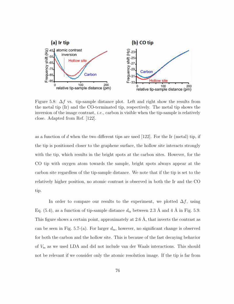
Figure 5.8: ∆f vs. tip-sample distance plot. Left and right show the results fromthe metal tip (Ir) and the CO-terminated tip, respectively. The metal tip shows theinversion of the image contrast, i.e., carbon is visible when the tip-sample is relativelyclose. Adapted from Ref. [122].
as a function of d when the two different tips are used [122]. For the Ir (metal) tip, if
the tip is positioned closer to the graphene surface, the hollow site interacts strongly
with the tip, which results in the bright spots at the carbon sites. However, for the
CO tip with oxygen atom towards the sample, bright spots always appear at the
carbon site regardless of the tip-sample distance. We note that if the tip is set to the
relatively higher position, no atomic contrast is observed in both the Ir and the CO
tip.
In order to compare our results to the experiment, we plotted ∆f , using
Eq. (5.4), as a function of tip-sample distance dts between 2.3 A and 4 A in Fig. 5.9.
This figure shows a certain point, approximately at 2.6 A, that inverts the contrast as
can be seen in Fig. 5.7-(a). For larger dts, however, no significant change is observed
for both the carbon and the hollow site. This is because of the fast decaying behavior
of Vts as we used LDA and did not include van der Waals interactions. This should
not be relevant if we consider only the atomic resolution image. If the tip is far from
76

2 2.5 3 3.5 4 4.5d
ts(Å)
∆f (
arb.
uni
t) HollowCarbon
Figure 5.9: Frequency shift with respect to the tip-graphene distance obtained byEq. (5.10) and Eq. (5.4)
the sample, in which the vdW interaction is dominant, no atomic resolution AFM
images are available.
This comparison implies that our simulation results are similar to the exper-
iment performed by a metal tip. This is consistent with the results that we present
in the next section about small molecules. Based on our observations on defect-free
graphene, we expect that our method predicts a similar contrast pattern obtained by
a metal tip for other graphene structures.
b. Single vacancy and Stone-Wales defect
To our knowledge, there is no atomic resolution AFM experiment currently available
for the graphene defects. Here, we present predictions for the nc-AFM images for a
few simple defect structures, which are frequently found in graphene [119].
A single vacancy can be found in any material. The atomic structure and
their AFM images are shown in Fig. 5.10-(a). There are two different types of single
vacancy structures with D3h and Cs symmetry. Cs symmetry can be found when
the reconstruction occurs around the vacancy [123]. In our simulation, we did not
77

observe the reconstructed configuration after the structural relaxation. The AFM
images were simulated with dts at 3 A, and we maintained this tip-sample distance
for all of the defect simulations. In Fig. 5.10-(a), the brightest spot is observed at the
vacancy site that has a pattern with a 3-fold symmetry.
Figure 5.10-(b) shows the Stone-Wales (SW) defect structure and the AFM
image. The SW defect is the simplest defect type that can occur by rearranging the
carbon atoms. As the hollow sites are imaged when we set a larger dts for graphene,
one might expect both pentagonal and heptagonal hollow sites of the SW defect to
appear as a bright spot in AFM. However, our simulation shows that the brightest
spot is located at the pentagonal hollow site rather than the heptagonal hollow site,
which is rather dark. This contrast difference between the pentagonal and the hep-
tagonal hollow sites should be useful in identifying the orientation of the SW defect
configuration.
Although both the single vacancy and the SW defect AFM images show the
bright spots at the defect hollow sites, the underlying physics may be different. In
order to explain our results, we composed a contour plot for the electron density at
1.5 A, 2.5 A, and 3.5 A distances from the graphene surface, and they are shown in
Fig. 5.11. Because of the conjugated π bond electrons, the electron density plot looks
like the honeycomb. For the single vacancy, however, higher electron density around
the single vacancy site is observed at 2.5 A and 3.5 A heights. For the single vacancy
structure with the D3h symmetry, previous DFT calculations showed the existence
of localized π orbitals lying on the single vacancy site [123], which looks very similar
to Fig. 5.11-(c) [124]. For the SW defect, the electron density is higher around the
heptagonal rings as shown in Fig. 5.11-(f).
In the previous section, we observed that the high electron density (π bond
78
of the carbon backbone) causes the bright spot when the tip is at the lower position.
Once the tip is positioned farther from the sample, hollow sites become less attractive
than carbon sites as the Pauli repulsion is no longer dominant at the carbon sites.
The same explanation can be applied for the AFM images of the defect structure.
Even though dts is set to 3 A in both cases, for the single vacancy case, the tip experi-
ences less attractive interaction owing to the high electron density. This explains the
observation of the bright spot at the vacancy site. For the SW defect, on the other
hand, the electron density is not found to be higher at any of the hollow sites. In this
case, the AFM image shows bright spots in which the electron density is lower than
other regions. This bright spot with low density is the hollow site. This explains why
our image shows the brightest spots at the pentagonal hollow site.
5.4 Small molecules
Remarkable advances in the AFM technique have enabled us to see very de-
tailed atomic structure of small molecules. Not only the bond order differences, but
also intermolecular hydrogen bonds have been detected by this technique [125, 126,
127]. The exact mechanism of how this technique, specifically with the CO func-
tionalized tip, achieves such a high resolution is still controversial. To address this
question, we performed AFM simulations for a few planar molecules. In particular,
we introduced the CO molecule as a model for the tip to compare two different AFM
simulation methods.
5.4.1 Computational details
All calculations we performed are based on the real-space pseudopotential
method. We utilized both the local density approximation (LDA) by Ceperley and
79

Figure 5.10: nc-AFM simulation results for two graphene defect structures. The tip-sample turning point is set to 3 A based on our results from the previous section.Yellow dots indicate the carbon atoms around the defects.
80
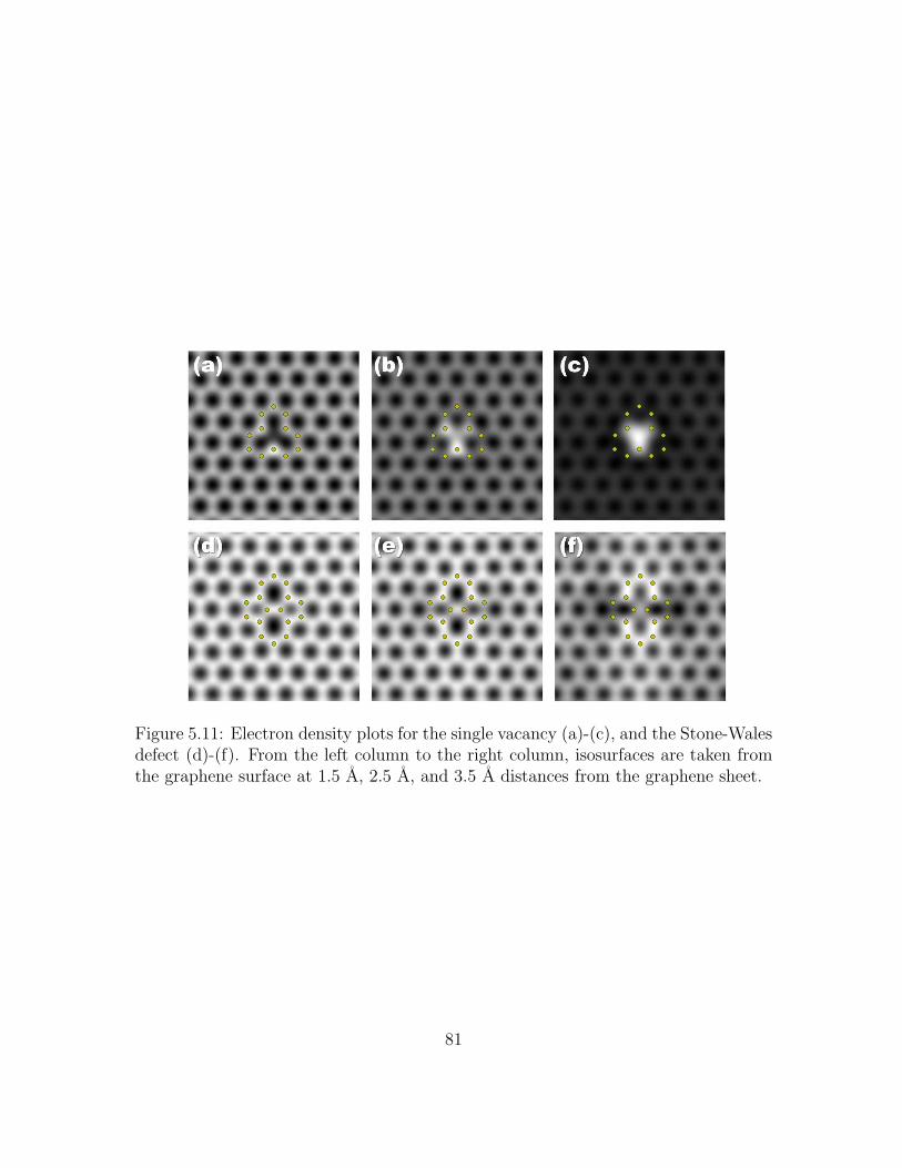
Figure 5.11: Electron density plots for the single vacancy (a)-(c), and the Stone-Walesdefect (d)-(f). From the left column to the right column, isosurfaces are taken fromthe graphene surface at 1.5 A, 2.5 A, and 3.5 A distances from the graphene sheet.
81

Alder [5], and the generalized gradient approximation (GGA) by Perdew-Burke-
Ernzerhof (PBE) [86] for the exchange correlation functional. For the GGA func-
tional, we added van der Waals force by following Tkatchenko-Scheffler scheme [128]
that does not require any preliminary determined parameters.2 Pseudopotentials
were generated with the same valence electron configuration and the cutoff radii as
we reported in the previous sections. Grid spacing was chosen to be 0.3 a.u. and all
structures were relaxed until the maximum force is less than 0.004 Ry/a.u. For the
tip model, we used only a CO molecule for a model for the CO-functionalized tip.
Several theoretical AFM studies have used the CO molecule attached to the metal
clusters such as Cu2CO. Our test for the choice of the tip finds no noticeable change
of the contrast in the AFM image between the Cu2CO and the CO tip models.
To simulate AFM images for the small molecules, we used a different equation
to calculate frequency shift (∆f). Most high resolution AFM experiments take the
measurement with a tip that oscillates with a very small amplitude [129, 126, 130].
To make our simulations more similar to them, we used Eq. 5.4, which is based on
the small amplitude oscillating motion of the tip.
5.4.2 Results and discussion
The choice of molecules was made from the recent nc-AFM experiment found
in the literature [127, 126]. Our first case is an 8-hydroxyquinoline (8-hq) molecule
(Fig. 5.12-(a)). This molecule was deposited on the Cu(111) surface either as an
individual molecule or randomly assembled aggregates [127]. One significant feature
of Zhang et al.’s work [127] is capturing the intermolecular hydrogen bond. Although
2This scheme was implemented in PARSEC by Ido Azuri in Prof. Leeor Kronik’s group atWeizmann Institute of Science.
82

this is a phenomenal observation, the individual molecule itself also possesses an
interesting feature in their AFM image. Figure 5.12-(a) shows the relaxed structure of
the 8-hq molecule. Fig. 5.12-(b) shows the AFM experiment adapted from Ref. [127].
One noticeable difference between the relaxed structure and measured AFM image
appears around the nitrogen atom (indicated as a blue circle in Fig. 5.12-(b)). The
relaxed structure shows that the N atom is slightly displaced toward to the O atom,
but the change remains relatively small. In the experimental AFM image, we make
two observations: the -OH group is almost invisible and the right side of the molecule
is vertically stretched. To investigate if the adsorbed 8-hq molecule goes through a
substantial structural relaxation, such as a distorsion, due to the Cu substrate, we
simulated AFM images with the 8-hq molecule without substrate, and the tip is set to
3.4 A above from the molecule using structure shown in (a). Our simulation images
are shown in Fig. 5.12-(d) which (d) was created by calculating force using Eq. 5.10,
and Fig. 5.12-(e), which was obtained by using the CO molecule as a tip model. In
this case, the frequency shift is calculated by using the equation∂2IE∂z2
where IE is
an interaction energy calculated with IE = E(8-hq+CO)-[(E(8-hq)+E(CO)] [131].
Both simulation methods resulted in the slightly stretched bright spots around
the N atom (toward to the H atom in the -OH group), and did also not image the
-OH group. In the previous section, we explained that the electron density is relevant
to the AFM image. The electron density at 3.4 A is shown in Fig 5.12-(c). This figure
confirms that the electron density contour plot shows a similar contrast to the AFM
images obtained from both of our simulation results.
The slightly elongated and shortened bond lengths have been reported in other
nc-AFM experiments as well. Gross and coworkers [126] reported that the bond or-
der, which is closely related to the bond length, of organic molecules such as C60 can
83

Figure 5.12: (a) 8-hydroxyquinoline molecule. (b) AFM experiment from Ref. [127].(c) Electron density contour plot at 3.4 A above from the molecule. (d) SimulatedAFM image without the explicit model for the tip. Tip height is set to 3.4 A. (e)Simulated frequency shift map by using CO tip. Tip height is set to 3.4 A.
84

be discriminated by nc-AFM. We chose one of the planar molecules from Ref. [126],
Dibenzo(cd,n)naphtho(3,2,1,8-para)perylene (DBNP), which is shown in Fig. 5.13-
(a). We performed the AFM simulations with two different methods, with and with-
out the AFM tip. Fig. 5.13-(d) and (e) present the AFM images simulated by without
the tip and with the CO tip, respectively. Even though both simulation methods de-
livered similar image contrast for the 8-hq molecule, in this DBNP case, we were
not able to observe the C-C bond in Fig. 5.13-(d) without the tip model. Interest-
ingly enough, this image shows a similar contrast obtained by the Xe tip experiment
(Fig. 5.13-(b)) [129]. Using the Xe tip, the C-C bonds are hardly visible unless it is
on the edge of the molecule. In fact, these results can be understood in the same
way as illustrated in graphene. In the graphene simulation, our method showed a
similar character to the Ir tip (metal tip) rather than the CO tip. Hence, we reaffirm
that our method that excludes an explicit model for the tip would bring comparable
results that we can expect from the metal tip.
5.5 Summary
In this chapter, we performed noncontact atomic force microscopy simulations.
We introduced an efficient method that can greatly reduce the computational costs
and eliminate the uncertainty of the tip morphology. Using this method, only one
fully self-consistent calculation is required to compose nc-AFM images. We tested our
method on various systems, from a semiconducting surface to hydrocarbon molecules.
We showed that our method can be applied to predict AFM images for the systems
in which the tip does not form a chemical bond with the substrate. For the carbon-
based systems such as graphene and organic molecules, our method is found to be
similar to the nc-AFM image obtained by a metal tip.
85

Figure 5.13: (a) Dibenzo(cd,n)naphtho(3,2,1,8-para)perylene molecule. (b)-(c) AFMexperiment from Ref. [129]. CO tip provides much higher resolution for C-C bondthan the Xe tip. (d) Simulated AFM image without the explicit model for the tip.Tip height is set to 3.4 A. (e) Simulated frequency shift map by using the CO tip.Tip height is set to 3.4 A. (f) Electron density contour plot at 3.4 A above from themolecule.
86

Bibliography
[1] P. Hohenberg and W. Kohn. Phys. Rev., 136:B864, 1964.
[2] W. Kohn and L. J. Sham. Phys. Rev., 140:A1133, 1965.
[3] K. Burke. J. Chem. Phys., 136:150901, 2012.
[4] R. M. Martin. Electronic Structure: Basic Theory and Practical Methods.
CAMBRIDGE, 2004.
[5] D. M. Ceperley and B. J. Alder. Phys. Rev. Lett., 45:566, 1980.
[6] J. P. Perdew and A. Zunger. Phys. Rev. B, 23:5048, 1981.
[7] N. Troullier and J. L. Martins. Phys. Rev. B, 43:1993, 1991.
[8] J. R. Chelikowsky. J. Phys. D: Appl. Phys., 33:R33–R50, 2000.
[9] B. Fornberg. Mathematics of compuatation, 51:699, 1988.
[10] J. R. Chelikowsky, N. Troullier, and Y. Saad. Phys. Rev. Lett., 72:1240, 1994.
[11] Y. Saad, J. R. Chelikowsky, and S. M. Shontz. SIAM Review, 52:3, 2010.
[12] Y. Zhou, Y. Saad, M. L. Tiago, and J. R. Chelikowsky. Phys. Rev. B,
74:066704, 2006.
[13] K. H. Khoo, M. Kim, G. Schofield, and J. R. Chelikowsky. Phys. Rev. B,
82:064201, 2010.
87

[14] Y. Zhou, Y. Saad, M. L. Tiago, and J. R. Chelikowsky. J. Comp. Phys.,
219:172, 2006.
[15] Y. Zhou, Y. Saad, M. L. Tiago, and J. R. Chelikowsky. Phys. Rev. E,
74:066704, 2006.
[16] A. Polman, D. C. Jacobson, D. J. Eaglesham, R. C. Kistler, and J. M. Poate.
J. Appl. Phys., 70:3778, 1991.
[17] J. Shieh, W. C. Yu, J. Y. Huang, C. K. Wang, B. T. Dai, H. Y. Jhan, C. W.
Hsu, H. C. Kuo, F. L. Yang, and C. L. Pan. Appl. Phys. Lett., 94:241108,
2009.
[18] Y. N. Xu and W. Y. Ching. Phys. Rev. B, 44:11048, 1991.
[19] F. Mauri, A. Pasquarello, B. G. Pfrommer, Y. G. Yoon, and S. G. Louie. Phys.
Rev. B, 62:R4786, 2000.
[20] S. von Alfthan, A. Kuronen, and K. Kaski. Phys. Rev. B, 68:073203, 2003.
[21] J. P. Rino, I. Ebbsjo, R. Kalia, A. Nakano, and P. Vashishta. Phys. Rev. B,
47:3053, 1993.
[22] T. Uchino, M. Takahashi, and T. Yoko. Phys. Rev. B, 62:2983, 2000.
[23] J. Sarnthein, A. Pasquarello, and R. Car. Phys. Rev. B, 52:12690, 1995.
[24] J. Sarnthein, A. Pasquarello, and R. Car. Phys. Rev. Lett., 74:4682, 1995.
[25] B. B. Karki, D. Bhattarai, and L. Stixrude. Phys. Rev. B, 76:104205, 2007.
[26] M. M. G. Alemany and J. R. Chelikowsky. Phys. Rev. B, 68:054206, 2003.
88

[27] J. R. Chelikowsky, J. J. Derby, V. V. Godlevsky, M. Jain, and J. Y. Raty.
Journal of Physics: Condensed Matter, 13:R817, 2001.
[28] K. Vollmayr, W. Kob, and K. Binder. Phys. Rev. B, 54:15808, 1996.
[29] K. H. Khoo, T.-L. Chan, M. Kim, and J. R. Chelikowsky. Phys. Rev. B,
84:214203, 2011.
[30] L. Kronik, A. Makmal, M. L. Tiago, M. M. G. Alemany, M. Jain, X. Huang,
Y. Saad, and J. R. Chelikowsky. phys. stat. sol., 243:1063, 2006.
[31] N. Binggeli, J. L. Martins, and J. R. Chelikowsky. Phys. Rev. Lett., 68:2956,
1992.
[32] M. M. G. Alemany, R. C. Longo, L. J. Gallego, D. J. Gonzalez, L. E. Gonzalez,
M. L. Tiago, and J. R. Chelikowsky. Phys. Rev. B, 76:214203, 2007.
[33] J. C. Tully, G. H. Gilmer, and M. Shugard. J. Chem. Phys., 71:1630, 1989.
[34] L. Martin-Samos, Y. Limoge, J.-P. Crocombette, G. Roma, N. Richard, E. Anglada,
and E. Artacho. Phys. Rev. B, 71:014116, 2005.
[35] A. Carre, J. Horbach, S. Ispas, and W Kob. Europhysics Letter, 82:17001,
2008.
[36] A. Einstein. Annalen der Physik, 17:549, 1905.
[37] J. R. Silva, D. G. Pinatti, C. E. Anderson, and M. L. Rudee. Philosophical
Magazine, 31:712, 1975.
89

[38] S. Susman, K. J. Volin, D. L. Price, M. Grimsditch, J. P. Rino, R. K. Kalia,
P. Vashishta, G. Gwanmesia, Y. Wang, and R. C. Liebermann. Phys. Rev. B,
43:1194, 1991.
[39] P. A. V. Johnson, A. C. Wright, and R. N. Sinclair. Journal of Non-Crystalline
Solids, 58:109, 1983.
[40] E. Dupree and R. F. Pettifer. Nature, 308:523, 1984.
[41] P. G. Coombs, J. F. D. Natale, P. J. Hood, E. K. McElfresh, R. S. Wortman,
and J. F. Schackelford. Philos. Mag. Lett., 51:L39, 1985.
[42] D. Ceresoli, M. Bernasconi, S. Iarlori, M. Parrinello, and E. Tosatti. Phys.
Rev. Lett., 84:3887, 2000.
[43] D. R. Hamann. Phys. Rev. B, 55:14784, 1997.
[44] T. Uchino, Y. Kitagawa, and T. Yoko. Phys. Rev. B, 61:234–240, 2000.
[45] G. Boureau and S. Carniato. Solid State Comm., 98:485–487, 1996.
[46] G. Pacchioni and G. Ierano. Phys. Rev. B, 56:7304, 1997.
[47] N. Capron, S. Carniato, A. Lagraa, G. Boureau, and A. Pasturel. J. Chem.
Phys., 112:9543, 2000.
[48] R. D. Bendale and L. L. Hench. Surface Science, 338:322, 1995.
[49] B. A. Morrow and I. A. Cody. J. Phys. Chem., 80:1995, 1976.
[50] T. A. Michalske and B. C. Bunker. J. Appl. Phys., 56:2686, 1984.
[51] J. M. Carpenter and D. L. Price. Phys. Rev. Lett., 54:441, 1985.
90

[52] A. Pasquarello and R. Car. Phys. Rev. Lett., 80:5145, 1998.
[53] B. Fischer, R. A. Pollak, T. H. DiStefano, and W. D. Grobman. Phys. Rev.
B, 15:3139, 1977.
[54] J. R. Chelikowsky and M. Schuter. Phys. Rev. B, 15:4020, 1977.
[55] R. B. Laughlin, J. D. Joannopoulos, and D. J. Chadi. Phys. Rev. B, 20:5228,
1979.
[56] S. T. Pantelides and W. A. Harrison. Phys. Rev. B, 13:2667, 1976.
[57] V. I. Klimov, S. A. Ivanov, J. Nanda, M. Achermann, I. Bezel, J. A. McGuire,
and A. Piryatinski. Nature, 447:441, 2007.
[58] X. Michalet, F. F. Pinaud, L. A. Bentolila, J. M. Tsay, S. Doose, J. J. Li,
G. Sun-daresan, A. M. Wu, S. S. Gambhir, and S. Weiss. Science, 307:538,
2005.
[59] I. Gur, N. A. Fromer, M. L. Geier, and A. P. Alivisatos. Science, 310:462, 2005.
[60] T. Takagahara and K. Takeda. Phys. Rev. B, 46:15578, 1992.
[61] A. Stadler. Materials, 5:661, 2012.
[62] R. G. Gordon. MRS bulletin, August2000:52, 2000.
[63] M. K. Singh, M. C. Mathpal, and A. Agarwal. Chem. Phys. Lett., 536:87,
2012.
[64] J. Suffner, P. Agoston, J. K., and H. Hahn. J. Nanopart. Res., 12:2579, 2010.
91

[65] D. G. Stroppa, L. A. Montoro, A. Beltran, T. G. Conti, R. O. da Silva, J. An-
dres, E. Longo, E. R. Leite, and A. J. Ramirez. J. Am. Chem. Soc., 131:14544,
2009.
[66] X. Xu, J. Zhuang, and X. Wang. J. Am. Chem. Soc., 130:12527, 2008.
[67] C.-T. Liu, W.-H. Lee, and T.-L. Shih. J. Nanotechnology, 2012:710908, 2012.
[68] H.-X. Deng, S.-S. Li, and J. Li. J. Phys. Chem. C, 114:4841, 2010.
[69] D. V. Melnikov and J. R. Chelikowsky. Phys. Rev. Lett., 92:046802, 2004.
[70] H. Kwak. Size-dependent properties of impurity doped semiconductor nanos-
tructures. PhD thesis, The University of Minnesota, 2009.
[71] P. D. Borges, L. M. R. Scolfaro, H. W. Leite Alves, and E. F. da Silva Jr.
Theor. Chem. Acc., 126:39, 2010.
[72] E. J. H. Lee, C. Ribeiro, T. R. Giraldi, E. Longo, and E. R. Leite. Appl. Phys.
Lett., 84:1745, 2004.
[73] M. Leslie and M. J. Gillan. J. Phys. C: Solid State Phys., 18:973, 1985.
[74] E. J. H. Lee, C. Ribeiro, T. R. Giraldi, E. Longo, E. R. Leite, and J. A. Varela.
Appl. Phys. Lett., 84:1745, 2004.
[75] G. M. Dalpian and J. R. Chelikowsky. Phys. Rev. Lett., 96:226802, 2006.
[76] T.-L. Chan, M. L. Tiago, E. Kaxiras, and J. R. Chelikowsky. Nano Lett., 8:596,
2008.
[77] S. Lany and A. Zunger. Phys. Rev. B, 78:235104, 2008.
92

[78] O. I. Velikokhatnyi and P. N. Kumta. Physica B, 406:471, 2011.
[79] U. zum Felde, M. Haase, and H. Weller. J. Phys. Chem. B, 104:9388, 2000.
[80] D. G. Stroppa, L. A. Montoro, A. Beltran, T. G. Conti, R. O. da Silva,
J. Andres, E. R. Leite, and A. J. Ramirez. Chem. Eur. J., 17:11515, 2011.
[81] N. S. Bobbitt, M. Kim, N. Marom, N. Sai, and J. R. Chelikowsky. (unpub-
lished).
[82] K. Nakataa and A. Fujishima. Journal of Photochemistry and Photobiology C:
Photochemistry Reviews, 13:169, 2012.
[83] H.-J. Zhai L.-S. Wang. Chem. Phys. Lett., 500:185, 2010.
[84] H.-J. Zhai and L.-S. Wang. J. Am. Chem. Soc., 129:3022, 2007.
[85] R. Gehrke and K. Reuter. Phys. Rev. B, 79:085412, 2009.
[86] J. P. Perdew, K. Burke, and M. Ernzerhof. Phys. Rev. Lett., 77:3865, 1996.
[87] V. Blum, R. Gehrke, F. Hanke, P. Havu, V. Havu, X. Ren, K. Reuter, and
M. Scheffler. Computer Physics Communications, 180:2175, 2009.
[88] N. Marom, M. Kim, and J. R. Chelikowsky. Phys. Rev. Lett., 108:106801,
2012.
[89] L. Hedin. Phys. Rev., 139:A796–A823, 1965.
[90] M. S. Hybertsen and S. G. Louie. Phys. Rev. B, 34:5390–5413, 1986.
[91] C. Adamo and V. Barone. J. Chem. Phys., 110:6158, 1999.
93

[92] L. Kronik, R. Fromherz, E. Ko, G. Gantefor, and J. R. Chelikowsky. Nature
Materials, 1:49, 2002.
[93] G. Binnig, H. Rohrer, Ch. Gerber, and E. Weibel. Phys. Rev. Lett., 49:57,
1982.
[94] G. Binnig, C. F. Quate, and Ch. Gerber. Phys. Rev. Lett., 56:930, 1986.
[95] W. R. Bowen and N. Hilal, editors. Atomic Force Microscopy in Process Engi-
neering. Elsevier, 2009.
[96] J. B. Pethica and W. C. Oliver. Phys. Scri. T, 19:61, 1987.
[97] F. Ohnesorge and G. Binnig. Science, 260:1451, 1993.
[98] Y. Martin, C. C. Williams, and H. K. Wickramasinghe. J. Appl. Phys.,
61:4723, 1987.
[99] T. R. Albrecht, P. Trutter, D. Horne, and D. Rugar. J. Appl. Phys., 69:668,
1991.
[100] T.-L. Chan, C. Z. Wang, K. M. Ho, and J. R. Chelikowsky. Phys. Rev. Lett.,
102:176101, May 2009.
[101] S. Morita, R. Wiesendanger, and E. Meyer, editors. Noncontact Atomic Force
Microscopy. Springer, 2002.
[102] G. H. Enevoldsen. PhD thesis, University of Aarhus, 2007.
[103] W. Melitz, J. Shen, A. C. Kummel, and S. Lee. Surface Science Reports, 66:1,
2011.
94

[104] R. Garcia and R. Perez. Surface Science Reports, 47:197–301, 2002.
[105] F. J. Giessibl. Phys. Rev. B, 56:16010, 1997.
[106] F. J. Giessibl. Appl. Phys. Lett., 78:123, 2001.
[107] S. G. Louie, S. Froyen, and M. L. Cohen. Phys. Rev. B, 26:1738, 1982.
[108] H. Kim and J. R. Chelikowsky. Surf. Sci., 409:435, 1998.
[109] J. L. A. Alves, J. Hebenstreit, and M. Scheffler. Phys. Rev. B, 44:6188, 1991.
[110] T. Ohno and K. Shiraishi. Phys. Rev. B, 42:11194, 1990.
[111] H. J. Monkhorst and J. D. Pack. Phys. Rev. B, 13:5188, 1976.
[112] A. Schwarz, W. Allers, U. D. Schwarz, and R. Wiesendanger. Phys. Rev. B,
61:2837, 2000.
[113] N. Uehara, H. Hosoi, K. Sueoka, and K. Mukasa. Nanotechnology, 15:S97,
2004.
[114] S. H. Ke, T. Uda, R. Perez, I. Stich, and K. Terakura. Phys. Rev. B, 60:11631–
11638, 1999.
[115] S. H. Ke, T. Uda, I. Stich, and K. Terakura. Phys. Rev. B, 63:245323, 2001.
[116] A. S. Foster, A. Y. Gal, J. M. Airaksinen, O. H. Pakarinen, Y. J. Lee, J. D.
Gale, A. L. Shluger, and R. M. Nieminen. Phys. Rev. B, 68:195420, 2003.
[117] A. H. Castro Neto, F. Guinea, N. M. R. Peres, K. S. Novoselov, and A. K.
Geim. Rev. Mod. Phys., 81:109, 2009.
95

[118] S. Das Sarma, S. Adam, E. H. Hwang, and E. Rossi. Rev. Mod. Phys., 83:407,
2011.
[119] F. Banhart, J. Kotakoski, and A. V. Krasheninnikov. ACS NANO, 5:26, 2011.
[120] M. J. Allen, V. C. Tung, and R. B. Kaner. Chem. Rev., 110:132, 2010.
[121] M. Ondracek, P. Pou, V. Rozsıval, C. Gonzalez, P. Jelınek, and R. Perez. Phys.
Rev. Lett., 106:176101, 2011.
[122] M. P. Boneschanscher, J. van der Lit, Z. Sun, I. Swart, P. Liljeroth, and D. Van-
maekelbergh. ACS NANO, 6:10216, 2012.
[123] H. Amara, S. Latil, V. Meunier, Ph. Lambin, and J.-C. Charlier. Phys. Rev.
B, 76:115423, 2007.
[124] H. Amara, S. Latil, V. Meunier, Ph. Lambin, and J.-C. Charlier. Phys. Rev.
B, 76:115423, 2007.
[125] D. G. de Oteyza, P. Gorman, Y. C. Chen, S. Wickenburg, A. Riss, D. J. Mow-
bray, G. Etkin, Z. Pedramrazi, H. Z. Tsai, A. Rubio, M. F. Crommie, and F. R.
Fischer. Science, 340:1434, 2013.
[126] L. Gross, F. Mohn, N. Moll, B. Schuler, A. Criado, E. Guitian, D. Pena,
A. Gourdon, and G. Meyer. Science, 337:1326, 2012.
[127] J. Zhang, P. Chen, B. Yuan, W. Ji, Z. Cheng, and X. Qiu. Science, 342:611,
2013.
[128] A. Tkatchenko and M. Scheffler. Phys. Rev. Lett., 102:073005, 2009.
96

[129] F. Mohn, B. Schuler, L. Gross, and G. Meyer. Appl. Phys. Lett., 102:073109,
2013.
[130] L. Gross, F. Mohn, N. Moll, P. Liljeroth, and G. Meyer. Science, 325:1110,
2009.
[131] C.-S. Guo, M. A. Van Hove, R.-Q. Zhang, and C. Minot. Langmuir, 26:16271,
2010.
[132] C. Barth, A. S. Foster, C. R. Henry, and A. L. Shluger. Advanced Materials,
23:477, 2011.
[133] J. K. Wassei and R. B. Kaner. Materials Today, 13:52, 2010.
97

Vita
Minjung Kim was born in Seoul, South Korea. After graduating from Seoul
Arts High School, she entered Seoul National University where she received Bachelor
of Science degree in Chemical and Biological Engineering with Physics minor. After
completing her undergraduate study, she entered graduate school at The University
of Texas at Austin in August 2008. She joined Professor James R. Chelikowsky’s
group in October 2008 and continued her work until May 2014.
Permanent email: [email protected]
This dissertation was typeset with LATEX† by Minjung Kim.
†LATEX is a document preparation system developed by Leslie Lamport as a special version ofDonald Knuth’s TEX Program.
98


