

Copyright Warning & Restrictions
The copyright law of the United States (Title 17, United States Code) governs the making of photocopies or other
reproductions of copyrighted material.
Under certain conditions specified in the law, libraries and archives are authorized to furnish a photocopy or other
reproduction. One of these specified conditions is that the photocopy or reproduction is not to be “used for any
purpose other than private study, scholarship, or research.” If a, user makes a request for, or later uses, a photocopy or reproduction for purposes in excess of “fair use” that user
may be liable for copyright infringement,
This institution reserves the right to refuse to accept a copying order if, in its judgment, fulfillment of the order
would involve violation of copyright law.
Please Note: The author retains the copyright while the New Jersey Institute of Technology reserves the right to
distribute this thesis or dissertation
Printing note: If you do not wish to print this page, then select “Pages from: first page # to: last page #” on the print dialog screen
The Van Houten library has removed some of the personal information and all signatures from the approval page and biographical sketches of theses and dissertations in order to protect the identity of NJIT graduates and faculty.

ABSTRACT
RELIABILITY STUDY OF Zr AND Al INCORPORATED Hf BASED HIGH-K
DIELECTRIC DEPOSITED BY ADVANCED PROCESSING
by
Md Nasir Uddin Bhuyian
Hafnium-based high- dielectric materials have been successfully used in the industry as
a key replacement for SiO2 based gate dielectrics in order to continue CMOS device scaling
to the 22-nm technology node. Further scaling according to the device roadmap requires
the development of oxides with higher values in order to scale the equivalent oxide
thickness (EOT) to 0.7 nm or below while achieving low defect densities. In addition, next
generation devices need to meet challenges like improved channel mobility, reduced gate
leakage current, good control on threshold voltage, lower interface state density, and good
reliability. In order to overcome these challenges, improvements of the high- film
properties and deposition methods are highly desirable.
In this dissertation, a detail study of Zr and Al incorporated HfO2 based high-
dielectrics is conducted to investigate improvement in electrical characteristics and
reliability. To meet scaling requirements of the gate dielectric to sub 0.7 nm, Zr is added
to HfO2 to form Hf1-xZrxO2 with x=0, 0.31 and 0.8 where the dielectric film is deposited
by using various intermediate processing conditions, like (i) DADA: intermediate thermal
annealing in a cyclical deposition process; (ii) DSDS: similar cyclical process with
exposure to SPA Ar plasma; and (iii) As-Dep: the dielectric deposited without any
intermediate step. MOSCAPs are formed with TiN metal gate and the reliability of these
devices is investigated by subjecting them to a constant voltage stress in the gate injection
mode. Stress induced flat-band voltage shift (VFB), stress induced leakage current (SILC)

and stress induced interface state degradation are observed. DSDS samples demonstrate
the superior characteristics whereas the worst degradation is observed for DADA samples.
Time dependent dielectric breakdown (TDDB) shows that DSDS Hf1-xZrxO2 (x=0.8) has
the superior characteristics with reduced oxygen vacancy, which is affiliated to electron
affinity variation in HfO2 and ZrO2. The trap activation energy levels estimated from the
temperature dependent current voltage characteristics also support the observed reliability
characteristics for these devices.
In another experiment, HfO2 is lightly doped with Al with a variation in Al
concentration by depositing intermediate HfAlOx layers. This work has demonstrated a
high quality HfO2 based gate stack by depositing atomic layer deposited (ALD) HfAlOx
along with HfO2 in a layered structure. In order to get multifold enhancement of the gate
stack quality, both Al percentage and the distribution of Al are observed by varying the
HfAlOx layer thickness and it is found that < 2% Al/(Al+Hf)% incorporation can result in
up to 18% reduction in the average EOT along with up to 41% reduction in the gate leakage
current as compared to the dielectric with no Al content. On the other hand, excess Al
presence in the interfacial layer moderately increases the interface state density (Dit). When
devices are stressed in the gate injection mode at a constant voltage stress, dielectrics with
Al/(Hf+Al)% < 2% show resistance to stress induced flat-band voltage shift (VFB), and
stress induced leakage current (SILC). The time dependent dielectric breakdown (TDDB)
characteristics show a higher charge to breakdown and an increase in the extracted Weibull
slope (β) that further confirms an enhanced dielectric reliability for devices with < 2%
Al/(Al+Hf)%.

RELIABILITY STUDY OF Zr AND Al INCORPORATED Hf BASED HIGH-K
DIELECTRIC DEPOSITED BY ADVANCED PROCESSING
by
Md Nasir Uddin Bhuyian
A Dissertation
Submitted to the Faculty of
New Jersey Institute of Technology
in Partial Fulfillment of the Requirements for the Degree of
Doctor of Philosophy in Electrical Engineering
Helen and John C. Hartmann Department of
Electrical and Computer Engineering
January 2015

Copyright © 2015 by Md Nasir Uddin Bhuyian
ALL RIGHTS RESERVED
APPROVAL PAGE
RELIABILITY STUDY OF Zr AND Al INCORPORATED Hf BASED HIGH-K
DIELECTRIC DEPOSITED BY ADVANCED PROCESSING
Md Nasir Uddin Bhuyian
Dr. Durgamadhab Misra, Dissertation Advisor Date
Professor of Electrical and Computer Engineering, NJIT
Dr. Leonid Tsybeskov, Committee Member Date
Professor of Electrical and Computer Engineering, NJIT
Dr. Marek Sosnowski, Committee Member Date
Professor of Electrical and Computer Engineering, NJIT
Dr. George Georgiou, Committee Member Date
Research Professor of Physics, NJIT
Dr. Kandabara Tapily, Committee Member Date
Senior Technical Staff Member,
Thin Film Process Technology Division, TEL
iv
BIOGRAPHICAL SKETCH Author: Md Nasir Uddin Bhuyian
Degree: Doctor of Philosophy
Date: January 2015
Undergraduate and Graduate Education:
Doctor of Philosophy in Electrical Engineering, New Jersey Institute of Technology, Newark, NJ, 2015
Master of Science in Electrical and Electronic Engineering, Bangladesh University of Engineering and Technology, Dhaka, Bangladesh, 2011
Bachelor of Science in Electrical and Electronic Engineering,
Bangladesh University of Engineering and Technology, Dhaka, Bangladesh, 2007 Major: Electrical Engineering Presentations and Publications: M.N. Bhuyian, D. Misra, K. Tapily, R. Clark, S. Consiglio, C. Wajda, G. Nakamura, and
G. Leusink, “Cyclic Plasma Treatment during ALD Hf1-xZrxO2 Deposition,” ECS Journal of Solid State Science and Technology, vol. 3, no. 5, p. N83, 2014.
M.N. Bhuyian, D. Misra, K. Tapily, R. Clark, S. Consiglio, C. Wajda, G. Nakamura, and
G. Leusink, “Reliability of ALD Hf1-xZrxO2 Deposited by Intermediate Annealing or Intermediate Plasma Treatment,” ECS Transactions, vol. 58, no. 7, p. 17, 2013.
M.N. Bhuyian, and D. Misra, “Reliability Considerations of High-κ Dielectrics Deposited
by Various Intermediate Treatment,” ECS Transactions, vol. 60, no. 1, p. 103, 2014. M.N. Bhuyian, D. Misra, K. Tapily, R. Clark, S. Consiglio, C. Wajda, G. Nakamura, and
G. Leusink, “Cyclic Plasma Treatment during ALD Hf1-xZrxO2 Deposition,” ECS Transactions, vol. 61, no. 2, p. 41, 2014.

v
M.N. Bhuyian, D. Misra, K. Tapily, R. Clark, S. Consiglio, C. Wajda, G. Nakamura, and
G. Leusink, “Effect of Al Doping on the Reliability of ALD HfO2,” ECS
Transactions, vol. 64, no. 8, p. 29, 2014.
M.N. Bhuyian and D. Misra “Reliability of Hf0.2Zr0.8O2 and HfO2 Films Deposited by
Cyclic Annealing or Cyclic Plasma Treatment” (Submitted to Microelectronics
Reliability).
M.N. Bhuyian and D. Misra, “ Multilayered ALD HfAlOx and HfO2 for High Quality Gate
Stack” (Submitted to IEEE Transactions on Device and Materials Reliability).
M.N. Bhuyian and D. Misra, “ Effect of Cyclic Plasma Treated Hf1-xZrxO2 on Interface
State Density” (Submitted to Solid State Electronics Journal).
M.N. Bhuyian and D. Misra, “ALD HfAlOx in Multi Layered Structure Gate Stack:
Reliability” (Submitted to 2015 IEEE International Reliability Physics
Symphosium).
M. N. Bhuyian, D. Misra, and S. Poddar, “Impact of Cyclic Plasma Treatment on Defects
in TiN/HfZrO/SiON/Si Gate Stacks,” (In preparation).
M.N. Bhuyian, D. Misra, K. Tapily, R. Clark, S. Consiglio, C. Wajda, G. Nakamura, and
G. Leusink, “Reliability of ALD Hf1-xZrxO2 Deposited by Intermediate Annealing
or Intermediate Plasma Treatment,” Semiconductors, Dielectrics and Metals for
Nanoelectronics 11, 224th ECS Meeting, San Francisco, CA, October 27 - November
1, 2013.
M.N. Bhuyian and D. Misra, “Cyclic Plasma Treatment during ALD Hf1-xZrxO2
Deposition,” Dielectrics for Nanosystems 6: Materials Science, Processing,
Reliability, and Manufacturing, 225th ECS Meeting, Orlando, FL, May 11-15, 2014.
M. N. Bhuyian and D. Misra, “Effect of Al Doping On The Reliability of ALD HfO2,”
Semiconductors, Dielectrics, and Metals for Nanoelectronics 12, 226th ECS
Meeting, Cancun, Mexico, Oct 5-9, 2014.
M.N. Bhuyian and D. Misra, “Reliability of Al Doped HfO2 with Multi Layered ALD
HfAlOx,” 2014 GSA Research Day Poster Presentation, New Jersey Institute of
Technology, Newark, NJ.
vi
S. Poddar, M.N. Bhuyian, and D. Misra, “Understanding Defects in TiN/HfZrO/SiON/Si
Gate Stacks,” 2014 Summer Research Program Poster Presentation, New Jersey
Institute of Technology, Newark, NJ.
S. Bhattacharya, I. Priyadharshini, A. Mohan, M.N. Bhuyian, D. Misra, “Reliability Of
ALD Hf1-xZrxO2 Deposited by Intermediate Plasma Treatment (DSDS) with
Nitrided Chemically Grown Interface and Plasma Oxynitride Interface,” 2013
Summer Research Program Poster Presentation, New Jersey Institute of
Technology, Newark, NJ.
D. Chattopadhyay, H. Chakraborty, J. Krishnasamy, M. N. Bhuyian, D. Misra,
“Characterization Of High-K Gate Dielectrics Using a MOS Capacitor,” 2012
Summer Research Program Poster Presentation, New Jersey Institute of
Technology, Newark, NJ.

vii
To my parents
viii
ACKNOWLEDGMENT
I would like to express my deepest appreciation to my dissertation advisor, Dr.
Durgamadhab Misra, for his guidance, constant support, and encouragement throughout
my Ph.D. studies. He not only guided me through my research, but also helped me
enormously to be independent. I want to express my gratitude to all my committee
members, Dr. Leonid Tsybeskov, Dr. Marek Sosnowski, Dr. George Georgiou, and Dr.
Kandabara Tapily for their valuable suggestions.
I would like to thank Dr. Kandabara Tapily, Dr. Robert Clark and other researchers
of TEL Technology Center, America, Albany, NY, for supplying devices and helpful
discussions for this research.
My colleagues and friends at NJIT have always given me technical and moral
support during this time of research work. I want to take this opportunity to thank Selina
Mala, Peter Paliwoda, Yiming Ding, Tazima Selim Chowdhuru, Hillol Debnath, and Tariq
M Arif.
I am grateful to my family members especially my elder brother D. M. Alamgir
Chowdhury Plabon for his constant support and encouragement since my childhood. I am
indebted to my parents, who taught me first the principles, to dream for best things in the
world and to be a good human being.
Finally, I want to thank my lovely wife, Faria Sharmin, for her single handed
support, patience, and encouragement that have made this endeavor easy to bear.
ix
TABLE OF CONTENTS
Chapter Page
1 INTRODUCTION, MOTIVATION AND OBJECTIVE………………… 1
1.1 Introduction…………………………………………………………. 1
1.2 Motivation and Approach…………………………………………… 6
1.3 Objectives…………………………………………………………… 9
1.4 Dissertation Organization……………………………………………
10
2 HfO2 BASED HIGH-K DIELECTRICS WITH ADVANCED
PROCESSING: CURRENT STATUS……………………………………..
12
2.1 Introduction………………………………………………………….. 12
2.2 Selection Criteria of High-Dielectric Materials……………………. 13
2.3 Alloying HfO2 and ZrO2…………………………............................... 15
2.4 Intermediate Treatment in High-Dielectric Deposition…………….. 21
2.5 Slot Plane Antenna (SPA) Plasma…………………………………... 22
2.6 Al Incorporation into HfO2………………………………………….. 23
2.6.1 HfAlOx Alloy Structures…………………………………… 24
2.6.2 Al2O3/HfO2 Bilayer Structures……………………………... 26
2.6.3 Problems with Excess Al Incorporation……………………. 30
2.7 Chapter Summary…………………………………………………… 32
3 DEVICE FABRICATION, PHYSICAL CHARACTERIZATION,
RELIABILITY ISSUES, AND EXPERIMENTAL DETAILS………….....
33
3.1 Introduction………………………………………………………….. 33
3.2 Zr Incorporation in HfO2 and Intermediate Treatments………………
33

x
TABLE OF CONTENTS
(Continued)
Chapter Page
3.2.1 Device Fabrication………………………………………….. 33
3.2.2 Fundamental Properties of Hf1-xZrxO2 Deposited by Different
Processing …………………………………………………...
35
3.3 Extremely Low Al Incorporation in HfO2............................................. 39
3.3.1 Device Fabrication- ALD Multi Layered Structure…………. 39
3.3.2 Physical Properties of HfAlOx Dielectrics ………………….. 41
3.4 Defects and Reliability of High-Dielectrics…………………………. 43
3.4.1 Constant Voltage Stress Induced Degradations…………….... 45
3.4.2 Time Dependent Dielectric Breakdown (TDDB)……………. 49
3.5 Electrical characterization and Reliability Study …………………… 53
3.5.1 Capacitance-Voltage (C-V) Measurement………………….. 54
3.5.2 Conductance Measurement…………………………………. 54
3.5.3 Current-Voltage (I-V) Measurement………………………... 55
3.5.4 Constant Voltage Stress (CVS) for Reliability Study……….. 55
3.5.5 Measurement Automation…………………………………... 57
3.6 Chapter Summary……………………………………………............... 58
4 ELECTRICAL CHARACTERIZATION OF ALD Hf1-xZrxO2 WITH
CYCLIC DEPOSITION AND ANNEALING (DADA), AND CYCLIC SPA
Ar PLASMA TREATMENT (DSDS)……………………………………….
59
4.1 Introduction………………………………………………………….. 59
4.2 Capacitance-Voltage Characteristics, EOT, and Flat-band Voltage … 60

xi
TABLE OF CONTENTS
(Continued)
Chapter Page
4.3 Gate Leakage Current Density Comparison………………………….. 64
4.4 Interface State Density, Dit Extraction by Conductance Method……. 66
4.4.1 Impact of Zr Addition and SPA Ar Plasma Exposure on Dit…. 67
4.4.2 Mid gap Dit Comparison for DSDS, DADA, and As-Dep
Processing…………………………………………………….
69
4.5 Chapter Summary……………………………………………………. 70
5 RELIABILITY STUDY OF ALD Hf1-xZrxO2 WITH CYCLIC
DEPOSITION AND ANNEALING (DADA), AND CYCLIC SPA Ar
PLASMA TREATMENT (DSDS)…………………………………………..
71
5.1 Introduction………………………………………………………….. 71
5.2 Impact of Constant Voltage Stress…………………………………… 72
5.2.1 Stress Induced Flat-band Voltage Shift (VFB)………………. 72
5.2.2 Stress Induced Leakage Current (SILC)…………………….. 76
5.2.3 Stress Induced Interface State Generation……………………. 80
5.2.4 Time Dependent Dielectric Breakdown……………………... 84
5.3 Effect of Quality of Interfacial Layer………………………………… 88
5.3.1 Interface State Density Comparison for SiON and Plasma
Oxynitride Interface…………………………………………..
90
5.4 High Temperature I-V Measurement………………………………… 92
5.4.1 Defect Energy Level Calculation…………………………….. 93
5.4.2 SILC Activation Energy……………………………………... 96
5.5 Chapter Summary……………………………………………………. 98
xii
TABLE OF CONTENTS
(Continued)
Chapter
Page
6 RELIABILITY STUDY OF DIELECTRICS WITH EXTREMELY LOW Al
INCORPORATION IN HfO2………………………………………………..
99
6.1 Introduction………………………………………………………….. 99
6.2 Electrical Characteristics of Multi Layered ALD HfAlOx…………… 101
6.2.1 C-V and I-V Characteristics………………………………….. 102
6.2.2 Equivalent Oxide Thickness (EOT), Flat-band Voltage (VFB),
and Leakage Current Density (Jg) Comparison……………….
103
6.2.3 Comparison of Interface State Density……………………….. 107
6.3 Reliability Study by Constant Voltage Stress………………………… 108
6.3.1 Impact of Stress on VFB, SILC and Dit………………………. 108
6.3.2 Comparison of TDDB Characteristics………………………... 113
6.4 Chapter Summary…………………………………………………….. 116
7 SUMMARY AND FUTURE WORK………………………………………. 117
7.1 Summary……………………………………………………………… 117
7.2 Future Work…………………………………………………………... 120
7.2.1 ALD Hf1-xZrxO2 and HfAlOx on Si Substrate…………………. 120
7.2.2 Zr and Al Incorporated Hf Based High- Dielectrics on High
Mobility Substrates……………………………………………
120
REFERENCES………………………………………………………………....... 122
xiii
LIST OF TABLES
Table Page
3.1 Composition of Hf and Al from XPS and Dielectric Thickness
Measured by SE……................................................................................
42
4.1 Comparison of Interface State Density, Dit at Mid Gap for Different
Dielectrics……………………………………………………………….
69
5.1 Weibull Slope for As-Dep and DSDS Hf1-xZrxO2 With Different Zr
Percentages…………………………………………………………….
86
5.2 Failure Time (T63%) for Different Dielectrics. (Five Devices from Each
Device Type Were Stressed in The Gate Injection Mode until Hard
Breakdown)……………………………………………………………...
88
5.3 Defect Activation Energy (Ea) for DSDS and As-Dep Hf1-xZrxO2 (x=0
and 0.8)………………………………………………………………….
95
5.4 Comparison of SILC Activation Energy (Ec) for DSDS and As-Dep Hf1-
xZrxO2 (x=0 and 0.8)……………………………………………………..
97
6.1 Comparison of Interface State Density, Dit in The Si Mid-gap Level….. 107
6.2 Power Exponent (n) for VFB, and Jg/Jg0, and Dit/Dit0 Comparison for
Different Dielectrics……………………………………………………..
111
6.3 Weibull Slope, β for Lot A (A1, A2, and A3), Lot B (B1, and B2) With
HfAlOx Layer and the Control Device, C With HfO2 Only……………..
114
xiv
LIST OF FIGURES
Figure Page
2.1 (a) Optical band gap vs dielectric constant (k) of candidate gate
dielectrics, and (b) Band offset with Si valence band (VB) and
conduction band (CB) as a function of dielectric constant for candidate
gate dielectrics…………………………………………………………
14
2.2 Temperature-composition phase diagram of HfO2- ZrO2……………. 15
2.3 XRD (left) and ATR-FTIR (right) spectra for HfZrO with various
compositions. The inset shows the volume fraction of monoclinic phase
decreases with increase in Zr fraction…………………………...
16
2.4 Typical C-V plot for Hf1-xZrxO2 for different Zr/(Hf+Zr) content. Inset
shows the magnified C-V plot to demonstrate the relationship between
EOT and Zr Content…………………………………………………
17
2.5 Comparison of gate leakage current for Hf1-xZrxO2 with different
Zr/(Hf+Zr) content……………………………………………………
18
2.6 Id-Vd characteristics of HfO2 and HfZrOx NMOSFET
(W/L=10umX10um). Devices were fabricated with TaxCy gate
dielectrics were annealed in N2 ambient at 10000C………………….
19
2.7 (a) Normalized PBTI Vt shift and (b) Hysteresis of TiN/ Hf1-
xZrxO2/SiO2 nMOSFET with different ZrO2 concentrations. ALD Hf1-
xZrxO2 deposited by using HfCl4, ZrCl4, and H2O precursors on in situ
steam grown SiO2/Si interface………………………………………..
20
2.8 Charge pumping current, Icp as a function of base voltage for HfO2 and
HfZrOx NMOSFET before (solid line) and after stress at 1.8 V for
1000s (dashed line)…………………………………………………….
20
2.9 A typical slot plane antenna plasma system………………………… 22
2.10 Crystallization temperature of Hf1-xAlxOy as a function of Al/(Al+Hf)%
in the dielectrics. Inset shows XRD plot at the on set of crystallization
for Hf1-xAlxOy with x= 0.09……………………………………………
24
xv
LIST OF FIGURES
(Continued)
Figure Page
2.11 Synchronous grazing in plane X ray diffraction pattern for (a) as
deposited ALD Hf1-xAlxOy, (b) annealed ALD Hf1-xAlxOy as a function
of Al/(Al+Hf)%......................................................................................
25
2.12 The XPS Hf 4f spectra of pure HfO2, HfAlOx alloy, and Al2O3/HfO2
stack, respectively, after 500°C RTA PDA for 30 s in N2 atmosphere.
All samples were deposited with total 40 ALD cycles. Both HfAlOx
and Al2O3/HfO2 were deposited with 26 ALD cycles for HfO2
deposition and 14 ALD cycles for Al2O3 deposition………………….
25
2.13 The intensity ratio of IIL/ISi obtained from XPS Si 2p core-level spectra
for pure HfO2, HfAlOx alloy, and Al2O3/HfO2 stack, respectively, after
PDA at different temperatures…………………………………………
27
2.14 The variation of EOT value of pure HfO2, HfAlOx alloy, and
Al2O3/HfO2 stack, respectively, as a function of PDA temperatures….
28
2.15 The variation of current density at VFB−1 volts as a function of PDA
temperatures for pure HfO2, HfAlOx alloy, and Al2O3/HfO2 stack on
Si, respectively………………………………………………………..
29
2.16 VFB –EOT plots for NiSi/HfxAl1-xOy/terraced SiO2/n-Si p-MOSFETs.
All samples were subjected to PDA at 8000C and post Si deposition
annealing at 10000C…………………………………………………..
30
2.17 Dependencies of Vth and hole mobility at both 0.3 and 0.7 MV/cm on
Al content in HfxAl1−xOy for NiSi/HfxAl1−xOy /SiO2(1 nm) / Si p-
MOSFETs. The closed circles stand for experimental Vth that takes Vfb
roll-up effects into consideration and the open circles stand for
estimated Vth that excludes Vfb roll-up effects, which have been
calculated qualitatively by comparing measured data with fitted linear
VFB-EOT relationship in Fig. 2.16…………………………………….
31
2.18 Defect levels within the bulk high-in the context of MOS energy-
band diagram…………………………………………………………
35
xvi
LIST OF FIGURES
(Continued)
Figure Page
3.1 (a) Device structure of TiN/Hf1-xZrxO2/SiON/p-Si MOSCAP, (b)
dielectric deposition with cyclic deposition and annealing (DADA)
cyclic SPA plasma exposure (DSDS)………………………………….
34
3.2 TEM images for (a) As-Dep HfO2, (b) DSDS HfO2, and (c) DSDS
Hf0.2Zr0.8O2…………………………………………………………….
36
3.3 a) GIIXRD spectra of DADA Hf1-xZrxO2 as a function of Zr% in the
dielectrics, b) intensity of monoclinic (110) diffraction peak as a
function of Zr/(Zr+Hf)% in the dielectrics…………………………….
37
3.4 (a) Dielectric thickness (filled symbols on left scale) and interfacial
layer (IL) thickness (open symbols on right scale) for MOSCAPs with
DSDS, DADA, and As-Dep HfO2 and Hf0.2Zr0.8O2, (b) Dielectric
thickness (filled symbols on left scale) and interfacial layer (IL) for Hf1-
xZrxO2 with x=0, 0.31, and 0.8 for DSDS and As-Dep processing
conditions………………………………………………………………
37
3.5 (a) Device structure for Al incorporation in HfO2, (b) Device
fabrication process flow…………………………………………..........
40
3.6 Defect levels within the bulk high-in the context of MOS energy-
band diagram…………………………………………………………...
44
3.7 (a) Band diagram showing positive charge formation in the dielectric
under stress in the gate injection mode, (b) Capacitance–voltage
characteristics of p-Si/SiO2 /ZrO2 /TiN structures measured before and
after constant gate voltage stress at -3.6 V for 400 s. Solid lines are fits
to the data using a computer simulation. Inset: Energetic distribution of
interface defects used for simulation of the C–V
characteristics………………………………………………………….
46
xvii
LIST OF FIGURES
(Continued)
Figure Page
3.8 Band diagram showing trap assisted tunneling (TAT) through high-
layer and direct tunneling (DT) through interfacial layer (IL) during
(a) positive gate bias and (b) negative gate bias. Electron tunneling is
shown by red line and hole tunneling is shown by blue line……………
48
3.9 Formation of percolation path (shaded spheres) due to trap generation
(b) Different breakdown regimes during constant voltage stress………
50
3.10 Dependence of Weibull slope β of the charge to breakdown, QBD on
oxide thickness……………………………………………………......
52
3.11 Stressing MOS capacitor at a constant voltage stress in the gate
injection mode…………………………………………………………
56
3.12 Basic arrangement for electrical measurement automation of a simple
two-terminal device, e.g., MOS-Capacitor…………………………….
57
4.1 Comparison of CV characteristics for (a) Hf0.2Zr0.8O2 with DSDS,
DADA and As-Dep samples and (b) HfO2 with DSDS, DADA and As-
Dep samples…………………………………………………………...
60
4.2 Flat-band voltage VFB, as a function of EOT for Hf0.2Zr0.8O2 and HfO2
with DSDS, DADA, and As-Dep processing………………………….
61
4.3 (a) Comparison of EOT for DSDS and As-Dep MOSCAPs with HfO2
(x=0), Hf1-xZrxO2 (x=0.31), and Hf1-xZrxO2 (x=0.8), (b) flat-band
voltage variation for the devices with intermediate SPA plasma and
without plasma as a function of zirconium percentage. Filled symbols
represent DSDS and open symbols represent As-Dep samples………..
63
4.4 Comparison of J-V characteristics of (a) DSDS, DADA, and As-Dep
Hf0.2Zr0.8O2 and, (b) DSDS, DADA, and As-Dep HfO2……………….
64
xviii
LIST OF FIGURES
(Continued)
Figure Page
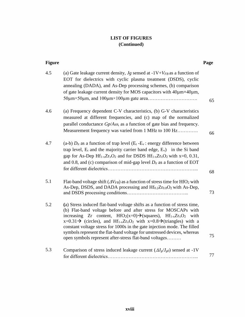
4.5 (a) Gate leakage current density, Jg sensed at -1V+VFB as a function of
EOT for dielectrics with cyclic plasma treatment (DSDS), cyclic
annealing (DADA), and As-Dep processing schemes, (b) comparison
of gate leakage current density for MOS capacitors with 40µm×40µm,
50µm×50µm, and 100µm×100µm gate area………………………….
65
4.6 (a) Frequency dependent C-V characteristics, (b) G-V characteristics
measured at different frequencies, and (c) map of the normalized
parallel conductance Gp/A, as a function of gate bias and frequency.
Measurement frequency was varied from 1 MHz to 100 Hz………….
66
4.7 (a-b) Dit as a function of trap level (Et -Ev : energy difference between
trap level, Et and the majority carrier band edge, Ev) in the Si band
gap for As-Dep Hf1-xZrxO2 and for DSDS Hf1-xZrxO2 with x=0, 0.31,
and 0.8, and (c) comparison of mid-gap level Dit as a function of EOT
for different dielectrics………………………………………………...
68
5.1 Flat-band voltage shift (VFB) as a function of stress time for HfO2 with
As-Dep, DSDS, and DADA processing and Hf0.2Zr0.8O2 with As-Dep,
and DSDS processing conditions………………………………...
73
5.2 (a) Stress induced flat-band voltage shifts as a function of stress time,
(b) Flat-band voltage before and after stress for MOSCAPs with
increasing Zr content, HfO2(x=0)(squares), Hf1-xZrxO2 with
x=0.31 (circles), and Hf1-xZrxO2 with x=0.8(triangles) with a
constant voltage stress for 1000s in the gate injection mode. The filled
symbols represent the flat-band voltage for unstressed devices, whereas
open symbols represent after-stress flat-band voltages………
75
5.3 Comparison of stress induced leakage current (Jg/Jg0) sensed at -1V
for different dielectrics………………………………………………...
77

xix
LIST OF FIGURES
(Continued)
Figure Page
5.4 Gate leakage current density for unstressed devices (closed symbols)
and for stressed devices (open symbols) for DSDS and As-Deposited
MOSCAPs with HfO2 (x=0), Hf1-xZrxO2 (x=0.31)), and Hf1-xZrxO2
(x=0.8) at a constant voltage stress for 1000s in the gate injection mode.
Post stress measurement (a) at EOX = 10 MV/cm and (b) at EOX = -10
MV/cm…………………………………………………………..
78
5.5 Interface state density, Dit in the Si-band gap for unstressed devices
(filled symbols with solid lines) and for stressed devices (open symbols
with dashed lines). Constant voltage stress was applied in the gate
injection mode for 1000s. Stress voltage was ranged between -3V to -
3.4V according to the variation of EOT and flat-band voltage shift for
different dielectrics………………………………………………...
81
5.6 Change in mid-gap Dit for As-Dep and DSDS Hf1-xZrxO2 with x=0,
0.31, and 0.8…………………………………………………………..
82
5.7 Interface state density, Dit in the mid gap level for unstressed devices
and for devices stressed with a constant voltage stress for 1000s……..
83
5.8 Breakdown characteristics during gate injection stress showing
electron trapping, soft breakdown and hard breakdown. Inset shows
progressive breakdown prior to hard breakdown for DSDS Hf1-xZrxO2
(x=0.8)…………………………………………………………………
85
5.9 Weibull plot of time to breakdown (TBD) for DSDS and As-Dep Hf1-
xZrxO2 with different Zr percentages…………………………………..
86
5.10 Comparison of VFB (filled symbols : left scale), and Jg@-1V+VFB (open
symbols: right scale) for DSDS Hf0.2Zr0.8O2 with SiON and plasma
oxynitride interfacial layers……………………………………………
89
xx
LIST OF FIGURES
(Continued)
Figure Page
5.11 Jg as a function of stress time for DSDS Hf0.2Zr0.8O2 with SiON and
plasma oxynitride interfacial layers, (b) comparison of stress induced
flat-band voltage shift (VFB) as a function of stress time……………..
89
5.12 (a) Dit in the Si band gap for SiON and plasma oxynitride interfacial
layer, and (b) change in mid gap Dit for two different type of interfacial
layer……………………………………………………………………
90
5.13 (a) Current voltage (I-V) characteristics at elevated temperatures, (b)
ln(Jg) as a function of ln(Eox) in the negative bias region………….
92
5.14 (a) Gate leakage current sensed at -0.5V for DSDS and As-Dep Hf1-
xZrxO2 (x=0 and 0.8), (b) ln(Jg/Eox) vs 1000/T (Arrhenius plot) for
different dielectrics…………………………………………………….
93
5.15 (a) Jg as a function of temperature for devices stressed at -2V for 500s,
(b) Arrhenius plots for different dielectrics……………………………
94
5.16 Arrhenius plot for SILC activation energy for HfO2 and Hf0.2Zr0.8O2
with DSDS and As-Dep processing conditions. Devices were stressed
at -2V in the gate injection mode for 500s…………………………….
97
6.1 (a) Capacitance voltage characteristics comparison for Lot A(A1, A2,
A3), Lot B(B1 and B2) and Lot C (control device) (b) gate voltage (V)
vs leakage current density (Jg) for different dielectrics for both Lot A,
and Lot B with HfAlOx in layered structure and for the control sample,
C with HfO2. PDA temperature was 8000C for these dielectrics (a-b).
Comparison of C-V and J-V plots for A2(20 Cy HfAlOx)with PDA
temperature variation are shown in (c) and (d)…………………………
102
6.2 (a)-(b) Flat-band voltage, VFB and gate leakage current, Jg sensed at -
1V+ VFB as a function of EOT for dielectrics annealed at 8000C.
Comparison for A2 with 20Cy HfAlOx annealed at 6800C, 7000C, and
8000C in (c)-(d). For possible variation analysis, three devices from
each device types are presented (a-d)………………………………….
104
xxi
LIST OF FIGURES
(Continued)
Figure Page
6.3 (a) –(b)Stress induced flat-band voltage shift and SILC as a function
of stress time for dielectrics annealed at 8000C. Applied stress voltage
in the gate injection mode was varied in the range -2.18V to -2.57V
according to EOT and VFB variation to have equal stress field across all
dielectrics. Evolution of VFB and SILC as a function of time for A2
annealed at 6800C, 7000C, and 8000C in (c)-(d)…………………….
108
6.4 Weibull plot of charge to breakdown, QBD for devices with Al
incorporation in HfO2. Inset shows Weibull plot for A2 with different
annealing temperatures………………………………………………...
113
1
CHAPTER 1
INTRODUCTION, MOTIVATION AND OBJECTIVES
1.1 Introduction
According to the International Technology Roadmap for Semiconductor (ITRS) 2013
updates [1], many physical dimensions of transistors are expected to be crossing the 10 nm
threshold in the years 2020-2025. Continuous device scaling leads to a decrease in cost per
function of technology and improves the economic productivity and the quality of life
through proliferation of computers, communication, and other industrial and consumer
electronics. With the scaling of devices below the 45 nm technology node, high- gate
dielectric materials emerged as a replacement of SiO2 in the high performance (HP) logic
family and low standby power (LSTP) logic family [2]. HfO2 based dielectric materials
have been considered as the most promising alternative of SiO2 in the CMOS technology
because of their quality superior to other high- dielectrics considering CMOS
compatibility, higher dielectric constant, suitable band offset with Si, and good thermal
stability with Si [2-3].
Although research on the high-metal gate (MG) started in mid 90s, the first
successful use of HfO2 as a dielectric in the high volume manufacturing industry emerged
in early 2007 by Intel in the 2007 processor series codenamed Penryn [4]. Research on
HK/MG is continuing to scale the equivalent oxide thickness (EOT) to sub 0.7 nm as well
to have better quality dielectrics [1-3]. Improvement came in the deposition process and
treatment during and after the deposition of gate stacks [5-16]. Further investigations were
2
carried out with incorporating other materials like Zr or Al into HfO2 in order to foster
device scaling and their performance enhancement [17-34].
Recently, various interleaved treatments in the ALD deposition process of Hf-based
high-k dielectrics have attracted tremendous attention in order to enhance the quality of
dielectrics for CMOS technology [5-11]. Multiple deposition and annealing was reported
to be beneficial for better film properties and enhanced device performance as compared
to a single post deposition annealing (PDA) [12-16]. The addition of Zr in HfO2 was also
shown to be beneficial for better EOT downscaling by several reports [17-21]. Recently,
Clark et al. [11] observed that the use of a cyclical deposition and annealing technique,
DADA, during the ALD HfO2 deposition could result in a better EOT downscaling with
one order of magnitude reduction in the gate leakage current as compared to the PDA HfO2.
The same DADA process was also extended to Hf1-xZrxO2 [35], which showed that this
process can result a tetragonal (111) fiber texture for Hf1-xZrxO2 with more than 50% Zr
addition in HfO2 in contrast to a random orientation in PDA films. It is known that among
different crystalline phases of HfO2 and ZrO2, the tetragonal phase offers a higher dielectric
constant as compared to the monoclinic phase which is the thermodynamically stable phase
for these dielectrics [3, 36]. For PDA Hf1-xZrxO2 films, a partial stabilization of the
tetragonal phase was also achieved for around 60% Zr/(Hf+Zr) [36]. It was found that the
addition of Zr in HfO2 decreases the grain size, which in turn decreases the driving force
for a tetragonal to monoclinic transition [36].
In addition to thermal annealing, interleaved treatment in the ALD deposition
process was found to enhance device performance by using room temperature ultraviolet
ozone, D2O radical, and remote microwave N2O plasma [5-6,8-10]. Recently, it has been

3
reported that the poor dielectric characteristics of CVD and ALD grown silicon oxide films
can be improved by exposing them to a slot-plane-antenna (SPA) plasma with various
gases such as O2/Ar, Ar, O2/He [37-39]. The SPA plasma provides a high-density plasma
with low electron temperature, where the radicals diffuse from the plasma generation
region to the wafer surface. The SPA plasma is also a very low damage plasma process
compared to conventional inductively coupled plasma (ICP) or electron cyclotron
resonance (ECR) plasma [39]. It was found that the SPA plasma helps better film
densification as well as improved interfacial layer growth [39-40]. This research has
utilized cyclic deposition and annealing (DADA), and cyclic deposition and SPA plasma
exposure (DSDS) during the ALD Hf1-xZrxO2 deposition process.
Another process of foreign material incorporation in HfO2 is to add Al in HfO2. The
incorporation of aluminum into HfO2 by forming (HfO2)1-x(Al2O3)x films [22-31] or
HfO2/Al2O3 bi-layers [23, 32-33] was reported to be promising for high- on silicon and
high mobility substrates. For ALD (HfO2)1-x(Al2O3)x films, Ho et al. (x: 0.25↔0.8) [26],
Yu et al. (x: 0.15↔0.33) [27], and Wilk et al. (x: 0.5 and 0.75) [28] demonstrated a
significant increase in the amorphous to polycrystalline transition temperature when
aluminum was incorporated into HfO2. This characteristic, in turn, helps to eliminate
electrical and mass transport along the grain boundaries. Also, Park et al. [25]
demonstrated an ALD Hf aluminate film with (002) oriented tetragonal phase stabilization
with increased dielectric constant by the addition of Al2O3 into HfO2. Recently, Tapily et
al. [34] reported a mixed structure of tetragonal and monoclinic phase formation for ALD
Hf1-xAlxOy (x=0 to 0.25) with 2Å lower EOT and one order of magnitude reduced gate
leakage current. Reductions in oxygen vacancy and in carbon in the film were also

4
observed for HfAlOx films [30, 41]. For HfO2/Al2O3 bilayer structures, Cho et al. [32], and
Nishimura et al. [33] showed an improved thermal stability for dielectrics annealed up to
9000C. A comparative study showed that incorporation of Al in the alloy form provides a
better EOT downscaling potential with a reduced gate leakage current as compared to the
bilayer form [23]. However, Al diffusion after annealing can introduce fixed charges near
the Si/SiO interface [42]. Also, an increased Al incorporation can shift flat-band voltage
by forming a dipole layer at high-/SiOx interface [43-45]. Therefore, in order to get
good control on the device threshold voltage for highly scaled transistors, an extremely low
Al incorporation is desirable.
Reliability is a critical concern for high- dielectrics in order to integrate them into
mainstream commercial integrated circuits. Gate stack reliability can be evaluated by
understanding the charge trapping behavior of the dielectric and its response to the
electrical stress [46-51]. Stress induced flat-band voltage shifts [49, 52] and stress-induced
leakage currents (SILC) [53-54] demonstrate the robustness of these films. HfO2 has been
widely studied for its reliability under different stress conditions [46-55]. HfO2 emerged as
an early favorite because of its slightly higher band gap and comparatively better thermal
stability as compared to ZrO2 [3]. As devices are now fabricated with an intentionally
grown interfacial layer [1-3], ALD Hf1-xZrxO2 can be considered as an alternative of HfO2
for next generation CMOS devices. Also, PDA Hf1-xZrxO2 showed reduced VT shift, lower
C-V hysteresis, and higher time to failure as compared to HfO2 [17, 21, 56]. As the cyclic
SPA plasma treatment (DSDS), and the cyclic thermal annealing (DADA) are promising,
impact of these intermediate treatment on the reliability of ALD HfO2 and Hf1-xZrxO2 needs
to be analyzed in detail. Although HfAlOx has been studied with both (HfO2)1-x(Al2O3)x
5
alloy structures and HfO2/Al2O3 bilayer structures, they did not meet reliability challenges
because of comparatively higher Al (more than 6% Al) incorporation in HfO2 [23-24, 57-
58]. For Al incorporated HfO2, Samanta et al. [57] studied electrical stress induced charge
carrier generation/trapping related degradation of HfAlOx/SiO2 for 1:1 weight ratio of
HfO2-Al2O3 incorporated in the high-/metal gate structure. Intrinsic time zero dielectric
breakdown characteristics of HfAlOx alloys (Al% ranged from 8 to 78%) for metal-
insulator-metal (MIM) capacitors were also studied [58]. But these studies did not address
the impact of Al incorporation on either the dielectric/metal gate interface or on the Si/SiOx
interface for the high-/metal gate devices in CMOS technology. A detailed study of the
reliability for the high-/metal gate with a variation in Al concentration near the high-
/metal gate interface and the Si/SiOx interface is, therefore, required. Additionally, since
the standard thermal process required for source/drain activation in CMOS devices can be
as high as 10000C [59], a post deposition annealing temperature variation can also impact
the dielectric.
Since Zr or Al incorporation in HfO2 and interleaved treatment processes are
promising, the reliability of these dielectrics needs to be investigated. The knowledge of
stress induced defects, defect activation energy, and charge to breakdown can improve the
understanding of their effects on device reliability. Also, it is known that even though the
EOT is successfully scaled in some processes, the performance of the MOS device strongly
depends on the quality of the interface between the silicon substrate and the interfacial
layer [60-64]. In addition, the process-induced interface traps also significantly influence
the long term reliability of the devices. Interface traps, the result of a structural
imperfection, act as generation/recombination centers with an energy distribution
6
throughout the silicon band gap. When the device is in operation, electrons or holes occupy
interface traps and contribute to the threshold voltage shift. They also contribute to leakage
current, low-frequency noise, reduced mobility, drain current, and transconductance [60].
It was found that under the NBTI stress, the density of generated traps is higher in the
proximity of the interfacial layer [61]. Minimizing the interface state degradation due to
the electrical stress during device operation is considered a critical task for the
semiconductor industry [62-64]. Density of interface states, Dit versus energy, E, at the
Si/IL interface provides a comprehensive understanding of the impact of various process
conditions on interface defects. Also, an understanding of the impact of electrical stress
on interface state generation for these dielectrics will help their integration in future CMOS
technology.
1.2 Motivation and Approach
In order to integrate new materials and processes to the emerging technology generations,
they needs to be tested for quality and reliability. The reliability of high-gate dielectric
stack is influenced by both the high-layer and the SiO2 like interfacial layer which forms
either spontaneously or intentionally in order to maintain a sufficient carrier mobility and
to facilitate the growth of the high-layer. The dielectric deposition process and
treatments have significant influence on the dielectric constant and thickness of both layers,
as oxygen vacancies and oxygen diffusion to the interface from the high- layer vary under
different conditions [65]. Also, control of the interface state density, Dit is another
reliability challenge for alternative high- dielectrics, which strongly depends on
processing conditions [60-64]. The impact of the SPA plasma treatment during the

7
deposition of ALD Hf1-xZrxO2 on the interfacial layer or at the interface has not been
thoroughly investigated yet. The impact of incorporated Al on Si/SiOx interface needs to
be addressed in detail. It was found that electron trapping is comparatively higher in
HK/MG stacks due to the presence of more oxygen vacancy defects [55]. Stress induced
flat-band voltage shift, SILC, and Dit can provide the important reliability information for
high- dielectrics deposited with advanced processing. Under the electrical stress, the
defect activation energy varies with different processing conditions [66-67]. High
temperature measurements can help to understand the evolution of the defect level with the
processing condition variation [66-68]. With the thinning of dielectric stacks, the time
dependent dielectric breakdown (TDDB) becomes a vital reliability issue, as an increased
gate leakage current degrades the TDDB reliability [55].
Even though Zr and Al incorporated dielectrics with advanced processing showed
potential towards the EOT downscaling, their reliability needs to be investigated. Also,
the reliability of dielectrics with intermediate treatments such as the cyclic SPA plasma
exposure, or the cyclic thermal annealing needs to be analyzed in detail to evaluate the
impact of these intermediate treatments. Therefore, this research attempts to find the effect
of Zr and Al incorporation into Hf based high-dielectrics and the effects of intermediate
treatments during the deposition process on the reliability of these dielectrics which would
help its integration in future CMOS technologies.
To understand the impact of Zr addition, ALD Hf1-xZrxO2 with x=0, 0.31, and 0.8
were deposited in nMOS capacitor with SiON interfacial layer and TiN metal gate. One set
of dielectrics were subjected to the cyclic deposition and annealing termed as DADA and
other set of dielectrics were subjected to the cyclic deposition and SPA Ar plasma exposure
8
termed as DSDS process. The control samples were deposited by standard as-deposition
process. Using two different type of interfacial layers, (i) chemically grown oxide followed
by radical flow nitridation (Chemox+RFN) and (ii) plasma oxynitride grown after
removing chemically grown oxide (COR+SPAON), the influence of the intermediate
plasma treatment on the interfacial layer was further investigated.
To incorporate extremely low percentage of Al in HfO2, ALD HfAlOx was
deposited in a layered structure along with ALD HfO2. Two different lots, Lot A with
HfAlOx as the top layer in a bilayer structure, and Lot B with HfAlOx as the intermediate
layer sandwiched between two HfO2 layers were studied along with the control sample C
without any HfAlOx layer. In this process, Al/(Al+Hf)% in the range <1% to ~7% was
obtained. Al concentration variation near the metal gate/high-k interface and near the
Si/SiO2 interface was obtained by changing the location and thickness of ALD HfAlOx
layer in a multilayered gate stack.
The reliability of these dielectrics were evaluated by subjecting them to a constant
voltage stress in the gate injection mode. The applied stress voltage was modified
according to the variation in EOT and flat-band voltage to have an equal field across all
dielectrics. The impact of stress on the flat-band voltage, the leakage current, and the
interface stress density was analyzed for different processing conditions for Zr or Al
incorporated HfO2. Also dielectrics were subjected to TDDB stress in the gate injection
mode.
9
1.3 Objectives
Maintaining the quality and the reliability of dielectric materials is a critical task.
Capacitance voltage (C-V) and current voltage (I-V) measurements are commonly used in
studying the gate oxide quality in detail. Typically high frequency C-V characteristics are
used to extract the EOT and the flat-band voltage (VFB). These parameters along with the
leakage current can be compared to understand the impact of Zr and Al incorporation in
HfO2 as well as variation in dielectrics processing conditions. For n-channel MOS
capacitors with high-k/metal gate stacks, typical reliability study includes the stress
induced flat-band voltage shift (VFB) [52-53, 60-61, 69], the stress induced leakage
current (SILC) [52-55], the stress induced interface state generation (Dit) [54, 70-73], and
the time dependent dielectric breakdown (TDDB) analysis [74-76]. A brief description of
the objective of this research is listed here.
1. To critically and comprehensively examine the effect of Zr and Al incorporation on the
dielectric constant and trap density for ALD HfO2 based high-dielectric materials.
2 To investigate the effect of cyclic SPA plasma treatment (DSDS) and cyclic deposition
and annealing (DADA), on equivalent oxide thickness, flat-band voltage, gate leakage
current, and interface state density for ALD Hf1-xZrxO2 with different Zr/(Hf+Zr)
percentages.
3 To analyze the reliability characteristics of the dielectrics by comparing stress induced
flat-band voltage shift (VFB), stress induced leakage current (SILC), stress induced
interface state generation (Dit), and time dependent dielectric breakdown (TDDB) for
different devices with addition of Zr and variation in processing conditions.
4 To observe the impact of Al on high-metal gate and Si/SiO2 interface by modulating
the thickness and location of ALD HfAlOx layer in a multi layered gate stack to
incorporate extremely low percentage of Al in HfO2.
5 To determine the effect of Al concentration and distribution variation in the dielectric
stack on the reliability.
6 To observe the impact of annealing temperature variation on the reliability of
dielectrics with Al doped HfO2.

10
7 To probe the effect of Zr and Al incorporation on the interfacial layer and interface
state density for different processing conditions.
8 To understand the statistical distribution of defects and traps in the dielectrics.
1.4 Dissertation Organization
Chapter 2 discusses the state of the art high-gate dielectrics for CMOS technology with
addition of Zr and Al in ALD HfO2 based dielectric materials. Recent work involving
intermediate treatments and different processing conditions in the deposition process have
been briefly discussed from the literature.
The fabrication process for Zr or Al incorporated MOS devices with the TiN metal
gate on the p-Si substrate used in the present work has been described in Chapter 3. Details
of physical characterization results and electrical characterization techniques are also
discussed here. The origin of defects and the reliability study for high-/metal gate devices
focusing on constant voltage stress and time dependent dielectric breakdown have been
also discussed.
Comparison of Electrical characteristics for Zr incorporated HfO2 are presented in
Chapter 4. Results from capacitance voltage (C-V) and current voltage (I-V) measurements
have been analyzed in detail. For different dielectrics, evolution of the EOT, the flat-band
voltage, the leakage current density, and the interface state density have been evaluated
and explained along with their physical properties explained in Chapter 4.
Chapter 5 deals with effects of the Zr addition in HfO2 on the reliability of metal
gate/high-IL based gate stacks at room temperature. Effects of the intermediate thermal
annealing and the intermediate SPA plasma on the reliability of Zr incorporated dielectrics
11
have been discussed by observing the stress induced flat-band voltage shift, the stress
induced leakage current, the time dependent dielectric breakdown and the stress induced
interface state generation at room temperature. Also, Defect levels extracted from I-V
measurements at elevated temperatures have been discussed. Reliability characteristics for
ALD Hf1-xZrxO2 with the intermediate SPA plasma treatment have been analyzed for x=0,
0.31, and 0.8 in detail. Furthermore, the impact of the quality of interfacial layer has been
discussed for the cyclic SPA plasma treated Hf0.2Zr0.8O2.
Chapter 6 talks about the effects of Al addition in HfO2 on the reliability of
TiN/HfAlOx/HfO2/IL/p-Si and TiN/HfO2/HfAlOx/HfO2/IL/p-Si for the variation in Al
concentration. The effect of HfAlOx thickness variation on the stress induced flat-band
voltage shift, the stress induced leakage current, the time dependent dielectric breakdown,
and the stress induced interface state generation have been discussed for both structures.
Also, the impact of PDA temperature variation on the reliability has been discussed for one
set of dielectrics.
Chapter 7 gives a summary of this research and an outline of the future work.

12
CHAPTER 2
HfO2 BASED HIGH- DIELECTRICS WITH ADVANCED
PROCESSING: CURRENT STATUS
2.1 Introduction
Modern microprocessors used in today’s world consist of hundreds of millions of Metal –
Oxide Semiconductor Filed Effect Transistors (MOSFET). Although this type of transistor
was proposed in 1928 by J. E. Lilienfield [77], early attempts to realize it in various
semiconductor materials were unsuccessful due to the presence of a large amount of surface
states at the interface between the semiconductor and the overlying insulator. The first
realization of the FET structure came in 1960 by D. Kahng [78]. The early FET was made
by using the interface between silicon (Si) and its native oxide silicon dioxide (SiO2) [78].
Amorphous SiO2 has a dielectric constant, = 3.9 and has very good insulating property
including large band gap (Eg= 9 eV) and large valence band and conduction band offsets
with Si along with a low density of intrinsic defects. SiO2 can be grown thermally on Si
with excellent control of the thickness and uniformity. Also, Si/SiO2 interface defect
centers can be efficiently passivated after post metallization anneals in a hydrogen
containing ambient. Past few decades witnessed a continuous improvement in the
performance and speed of integrated circuits with the advent of Complementary Metal
Oxide Metal-Oxide Silicon (CMOS) technology in the semiconductor industry. According
to the Moor’s law of scaling [79], the number of devices on an integrated circuit increases
exponentially, doubling over two or three year period which requires the supply voltage,
the channel length, and the physical thickness of the dielectrics to be scaled down
accordingly. Apart from a better performance and higher speed, device scaling minimizes
13
cost of integration at the same time [80]. According to the International Technology
Roadmap for Semiconductor (ITRS) specifications [1], future generation MOSFET for
both high performance logic application and low operating power logic applications will
have the equivalent oxide thickness (EOT) below 1 nm. However, scaling SiO2 beyond 1
nm increases the gate leakage current significantly due to quantum mechanical tunneling.
Also, SiO2 losses bulk electronic properties when it becomes thinner than around 0.7 nm
[81]. Moreover, reliability is a critical issue as reduction of physical thickness allows large
amount of defect generation in the dielectric and the interface due to a higher leakage
current. Consequently, dielectrics go to early breakdown resulting in the failure of the
devices [82-86]. Hence, the earlier motivation for the use of high- dielectrics was to
simply reduce the gate leakage current while using thicker oxide for the same oxide
capacitance. The successful integration of high-dielectrics in CMOS industry became
possible after numerous research on potential high-dielectric materials. For example,
some dielectrics showed higher flat-band voltage shift due to the presence of
uncompensated charge or dipoles. Some other dielectrics were found to be unstable with
Si substrate [2]. Therefore, in order to be qualified for use in CMOS technology, high-
dielectric materials need to meet certain requirements.
2.2 Selection Criteria of High-Dielectric Materials
To maximize the performance and efficiency of devices with high--dielectric material
in advanced CMOS technologies, apart from higher dielectric constant, the potential
material should satisfy the following requirements [87]:
good thermal stability in contact with Si, so that the material does not form silicide
layers and thick layer of interfacial SiOx;

14
low intrinsic defect density in the bulk and interface;
large barrier height and band offsets with Si and consequently reduced gate leakage
current;
allows high carrier mobility in the channel;
good reliability;
compatibility with CMOS processing.
Figure 2.1 (a) Optical band gap vs dielectric constant (k) of candidate gate dielectrics, and
(b) Band offset with Si valence band (VB) and conduction band (CB) as a function of
dielectric constant for candidate gate dielectrics.
Source: [3].
Figure 2.1 shows the relation between optical band gap (Figure 2.1(a)) , band offset
(Figure 2.1 (b)) as a function of dielectric constant for candidate dielectric materials to
replace SiO2. Among various candidates, HfO2 and ZrO2 were considered as potential
replacement of SiO2 because they have high dielectric constant (~25-30 which is ~6-7
times of SiO2), energy band gap of around 5.8 eV with band offsets greater than 1 eV [2-
3]. In case of HfO2, the free energy of reaction with Si is about 47.6 Kcal/mol at 720oC
making it more stable material on Si substrate in comparison to other high-dielectrics.
(a)
(b)
15
Also, the silicide of Hf can be easily oxidized to form HfO2 [88]. All these properties of
HfO2 make it an attractive alternative for SiO2.
2.3 Alloying HfO2 and ZrO2
HfO2 and ZrO2 have been investigated extensively as possible alternatives to SiO2-based
options due to their relatively higher dielectric constants and larger band gap [87, 89-90].
Zr and Hf both are in group IV in the periodic table and are considered to be the two most
similar elements in the periodic table.
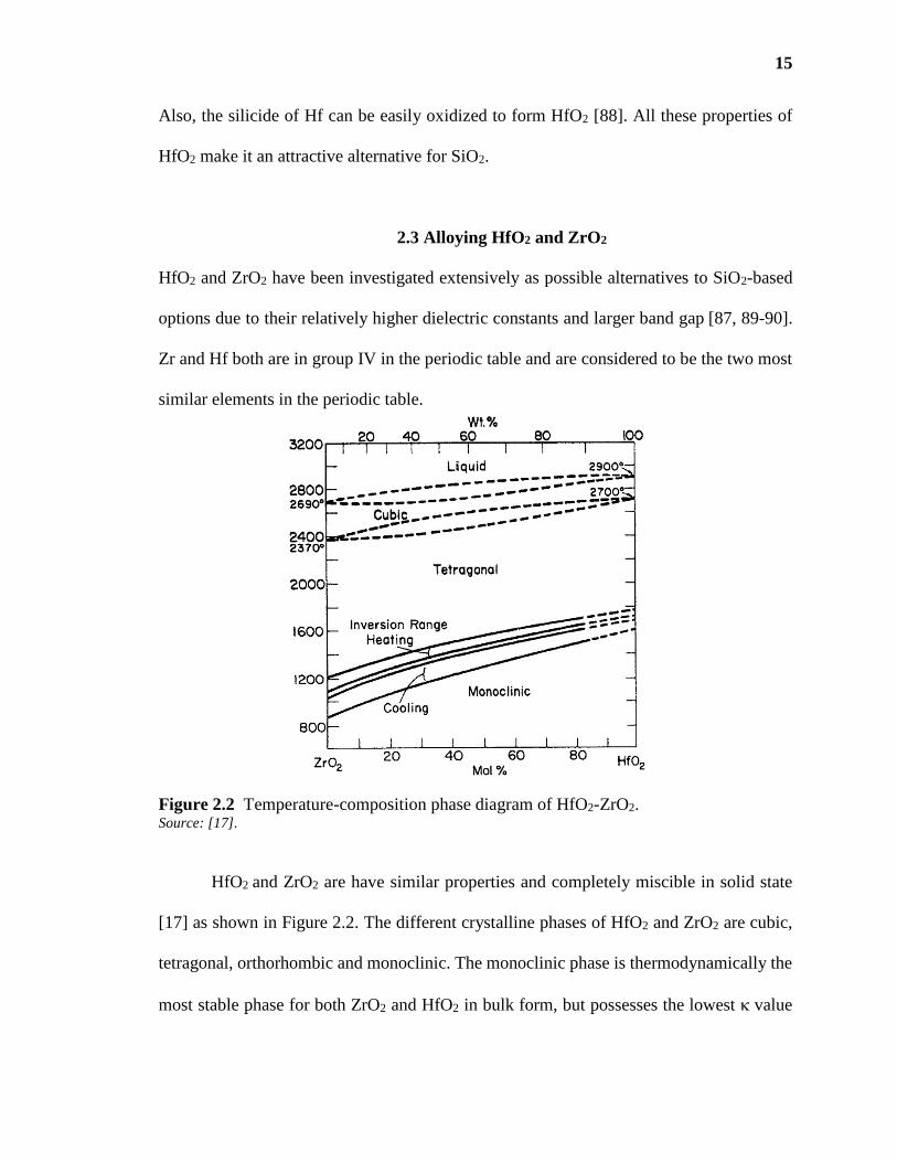
Figure 2.2 Temperature-composition phase diagram of HfO2-ZrO2. Source: [17].
HfO2 and ZrO2 are have similar properties and completely miscible in solid state
[17] as shown in Figure 2.2. The different crystalline phases of HfO2 and ZrO2 are cubic,
tetragonal, orthorhombic and monoclinic. The monoclinic phase is thermodynamically the
most stable phase for both ZrO2 and HfO2 in bulk form, but possesses the lowest value

16
[3]. The amorphous phase also exhibits a similar value as the monoclinic phase [91]. For
both ZrO2 and HfO2 the cubic phase has a higher value than monoclinic while the
tetragonal phase has the highest value due to the lower phonon frequencies and higher
effective charges [91].When HfO2 and ZrO2 are grown on Si substrate, it was found that,
ZrO2 has a slightly higher tendency to form silicide as compared to HfO2 [92-93]. For this
reason, HfO2 has been preferred in the high volume manufacturing industry [92-93].
However, the use of metal gate and an intentionally grown SiO2 rich interfacial layer (IL)
in modern CMOS devices has minimized the risk of silicide formation for dielectrics with
ZrO2 [94]. Therefore, the use of ZrO2 can be advantageous for the EOT downscaling as
ZrO2 has higher dielectric constant than HfO2, while both of them have similar band offsets
with Si [3]. Tetragonal stabilization of HfO2 by the addition of ZrO2 was reported by several
groups [17-20, 95].
Figure 2.3 XRD (left) and ATR-FTIR (right) spectra for HfZrO with various
compositions. The inset shows the volume fraction of monoclinic phase decreases with
increase in Zr fraction. Source: [95].

17
Figure 2.3 shows the X-ray diffraction (XRD) pattern (left) and the attenuation total
reflection Fourier transform infrared (ATR-FTIR) measurement results (right) for the
HfZrO alloy with different Hf/Zr ratio [95]. The observed results in Figure 2.3 clearly
shows the stabilization of higher-tetragonal phase with addition of ZrO2 into HfO2.
In addition of higher - crystalline structure formation, improved reliability of ALD
Hf1-xZrxO2 dielectrics as compared to HfO2 is also reported [17-21, 56]. It was also found
that addition of Zr to HfO2 can reduce the thickness of the dielectric layer by limiting the
interfacial layer regrowth [17, 35]. Consequently, Zr addition into HfO2 contributes toward
a lower EOT value.
Figure 2.4 Typical C-V plot for Hf1-xZrxO2 for different Zr/(Hf+Zr) content. Inset shows
the magnified C-V plot to demonstrate the relationship between EOT and Zr content.
Source: [21].
Figure 2.4 shows typical capacitance voltage characteristics for ALD Hf1-xZrxO2
deposited by using HfCl4, ZrCl4, and H2O precursors on in situ steam grown SiO2/Si
Ca
pa
cita
nce
(
F/c
m2)

18
interface [21] and annealed in nitrogen ambient at 10500C . Inset in Figure 2.4 shows an
increase in Cox or decrease in EOT with increase in Zr percentage.
Figure 2.5 shows the comparison of gate leakage current density for Hf1-xZrxO2
with different Zr/(Hf+Zr) content from ref. [21]. A slight increase in Jg with increasing Zr
content reveals that Zr incorporation into HfO2 modifies the band gap and the band offset,
as ZrO2 has comparatively a lower value of the band gap and the conduction band offset
with Si [2-3].
Figure 2.5 Comparison of gate leakage current for Hf1-xZrxO2 with different Zr/(Hf+Zr)
content.
Source: [21].
19
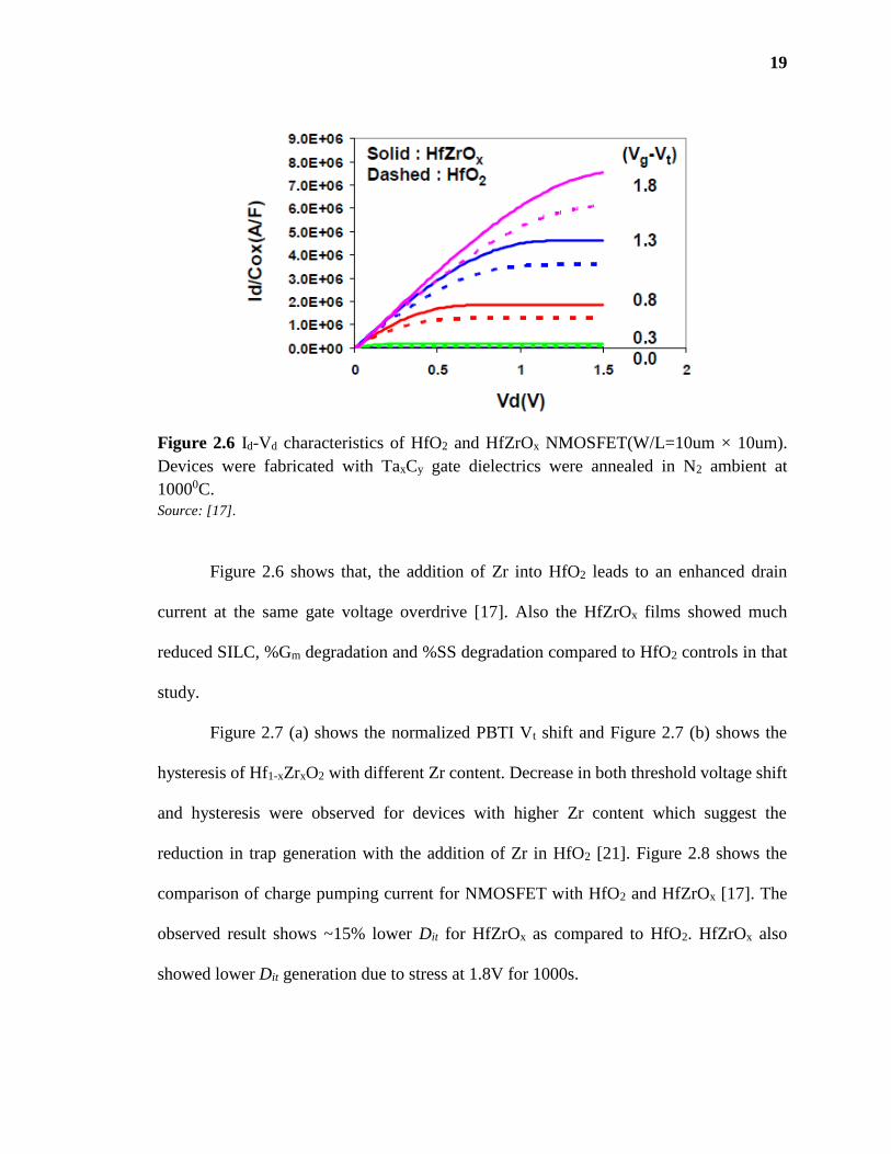
Figure 2.6 Id-Vd characteristics of HfO2 and HfZrOx NMOSFET(W/L=10um × 10um).
Devices were fabricated with TaxCy gate dielectrics were annealed in N2 ambient at
10000C.
Source: [17].
Figure 2.6 shows that, the addition of Zr into HfO2 leads to an enhanced drain
current at the same gate voltage overdrive [17]. Also the HfZrOx films showed much
reduced SILC, %Gm degradation and %SS degradation compared to HfO2 controls in that
study.
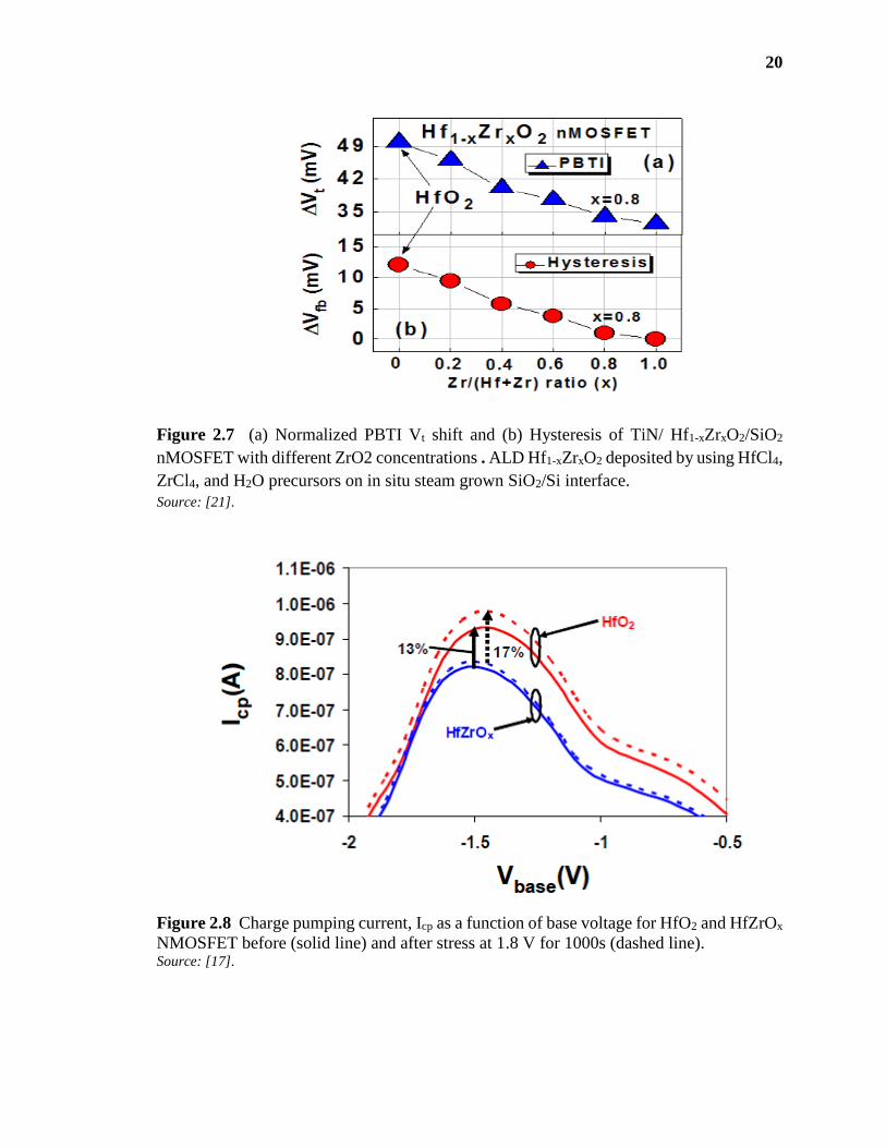
Figure 2.7 (a) shows the normalized PBTI Vt shift and Figure 2.7 (b) shows the
hysteresis of Hf1-xZrxO2 with different Zr content. Decrease in both threshold voltage shift
and hysteresis were observed for devices with higher Zr content which suggest the
reduction in trap generation with the addition of Zr in HfO2 [21]. Figure 2.8 shows the
comparison of charge pumping current for NMOSFET with HfO2 and HfZrOx [17]. The
observed result shows ~15% lower Dit for HfZrOx as compared to HfO2. HfZrOx also
showed lower Dit generation due to stress at 1.8V for 1000s.
20
Figure 2.7 (a) Normalized PBTI Vt shift and (b) Hysteresis of TiN/ Hf1-xZrxO2/SiO2
nMOSFET with different ZrO2 concentrations . ALD Hf1-xZrxO2 deposited by using HfCl4,
ZrCl4, and H2O precursors on in situ steam grown SiO2/Si interface.
Source: [21].
Figure 2.8 Charge pumping current, Icp as a function of base voltage for HfO2 and HfZrOx
NMOSFET before (solid line) and after stress at 1.8 V for 1000s (dashed line). Source: [17].
21
2.4 Intermediate Treatment in High-Dielectric Deposition
High-dielectrics deposited with various intermediate treatments were shown to be
beneficial in several reports [5-15, 96-100]. Multiple deposition and annealing of HfO2
film deposited with metal oxide chemical vapor deposition (MOCVD) was reported by
Yeo et al. [96] (700◦C anneal) and Ishikawa et al. [14] (750–950◦C anneal). Compared to
other processes, the atomic layer deposition (ALD) process provides an excellent thickness
control, a better conformity, and a low temperature deposition for Hf1-xZrxO2 [15, 97]. The
ALD film is grown through sequential saturated surface reactions and each ALD cycle
deposits a fixed amount, most often a part of a monolayer of the film on the surface [98].
Performance benefits of the intermediate thermal treatment were also reported for the ALD
grown dielectrics. Nabatame et al. [12] have demonstrated a device performance benefit
from performing an in-situ annealing (650◦C) after each ALD cycle during the growth of
HfAlOx films, deposited using an Hf-alkylamide precursor. Delabie et al. [10] also reported
that intermediate thermal treatments (420–500◦C), applied to the HfCl4/H2O process, led
to a significant reduction in in-film Cl content, whereas a PDA treatment led to no Cl
reduction. Clark et al. [11] observed almost ten-fold reduction in gate leakage current using
HfO2 gate oxide with multiple intermediate thermal treatments as compared to a single post
deposition annealing.
Apart from thermal treatment, an interleaved treatment in the ALD deposition
process by using room temperature ultraviolet ozone [5-7], D2O radical [8-9], and remote
microwave N2O plasma [10] were reported to enhance the device performance.
22
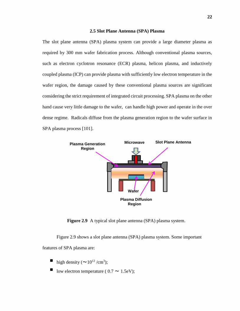
2.5 Slot Plane Antenna (SPA) Plasma
The slot plane antenna (SPA) plasma system can provide a large diameter plasma as
required by 300 mm wafer fabrication process. Although conventional plasma sources,
such as electron cyclotron resonance (ECR) plasma, helicon plasma, and inductively
coupled plasma (ICP) can provide plasma with sufficiently low electron temperature in the
wafer region, the damage caused by these conventional plasma sources are significant
considering the strict requirement of integrated circuit processing. SPA plasma on the other
hand cause very little damage to the wafer, can handle high power and operate in the over
dense regime. Radicals diffuse from the plasma generation region to the wafer surface in
SPA plasma process [101].
Figure 2.9 A typical slot plane antenna (SPA) plasma system.
Figure 2.9 shows a slot plane antenna (SPA) plasma system. Some important
features of SPA plasma are:
high density (~1012 /cm3);
low electron temperature ( 0.7 ~ 1.5eV);
Plasma Generation
Region
Plasma Diffusion Region
Slot Plane Antenna Microwave
Wafer

23
wide process window (7~1000Pa);
optional bias to accelerate ions.
The planar antenna structure of SPA plasma system is advantageous in realizing a compact
apparatus for semiconductor processing. There are several reports showing performance
improvement achieved by using SPA plasma in dielectric processing. Nagata et al. [37]
demonstrated that SPA plasma (Ar/O2) treatment results in better densification of CVD
SiO2. Kobayashi et al. [40] used SPA radical oxidation to produce improved GeO2
interfacial layer growth with no substrate orientation dependence. Decrease in gate leakage
current and trap density due to SPA plasma exposure was also reported by Kawase et al.
[38]. Tanimura et al. [39] reported reliability enhancement of ALD SiO2 by exposing it to
SPA plasma. In this work, we employed an interleaved treatment in the ALD Hf1-xZrxO2
deposition process by using Ar plasma in the SPA system in a cyclical deposition and
plasma treatment process, termed as DSDS. Unlike N2O or ultraviolet ozone, SPA Ar
plasma does not induce interfacial oxide growth that limits scaling potentials of such
processes [5-7, 10].
2.6 Al Incorporation into HfO2
Scaling below 22 nm technology node requires gate dielectric materials with properties
superior to those of conventional high-materials. Al2O3 has been used to improve the
thermal stability of high-HfO2 films [26-27]. It was found that Al incorporation into HfO2
results increase in transition temperature from amorphous to polycrystalline state [22, 26-
29, 34]. HfO2 has comparatively lower crystallization temperature than Al2O3 [22, 27].
Therefore, HfO2 allows lower thermal budget after its deposition, as polycrystalline grain

24
boundary induced leakage current and lateral nonuniformity increases after PDA at high
temperature [22, 27].
2.6.1 HfAlOx Alloy Structures
Figure 2.10 shows the effect of Al incorporation in HfO2 on the crystallization temperature
[34]. It was found that HfO2 starts to crystallize at around 6800C, while Hf1-xAlxOy with
25% Al/(Al+Hf) starts to crystallize at around 10000C. It was found that Al acts as a
network modifier and stabilizes the amorphous phase of the metal oxides [22]. In addition,
enhancement in the dielectric constant of ALD HfO2 due to Al incorporation by inserting
few Al-O ALD cycles in the ALD process was also reported [25, 34].
Figure 2.10 Crystallization temperature of Hf1-xAlxOy as a function of Al/(Al+Hf)% in the
dielectrics. Inset shows XRD plot at the on set of crystallization for Hf1-xAlxOy with x=
0.09. Source: [34].
25
Figure 2.11 Synchronous grazing in plane X ray diffraction pattern for (a) as deposited
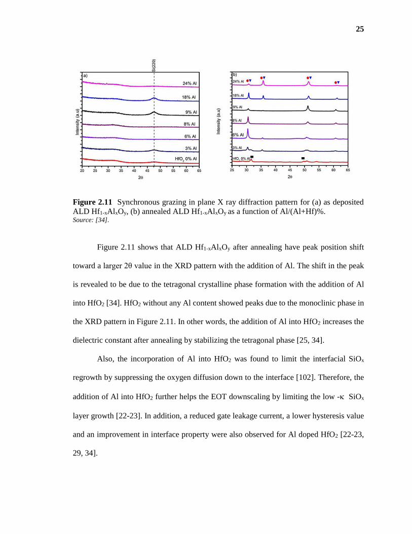
ALD Hf1-xAlxOy, (b) annealed ALD Hf1-xAlxOy as a function of Al/(Al+Hf)%. Source: [34].
Figure 2.11 shows that ALD Hf1-xAlxOy after annealing have peak position shift
toward a larger 2θ value in the XRD pattern with the addition of Al. The shift in the peak
is revealed to be due to the tetragonal crystalline phase formation with the addition of Al
into HfO2 [34]. HfO2 without any Al content showed peaks due to the monoclinic phase in
the XRD pattern in Figure 2.11. In other words, the addition of Al into HfO2 increases the
dielectric constant after annealing by stabilizing the tetragonal phase [25, 34].
Also, the incorporation of Al into HfO2 was found to limit the interfacial SiOx
regrowth by suppressing the oxygen diffusion down to the interface [102]. Therefore, the
addition of Al into HfO2 further helps the EOT downscaling by limiting the low - SiOx
layer growth [22-23]. In addition, a reduced gate leakage current, a lower hysteresis value
and an improvement in interface property were also observed for Al doped HfO2 [22-23,
29, 34].
26
2.6.2 Al2O3/HfO2 Bilayer Structures
In addition of getting better thermal stability by Al incorporation in the form of HfAlOx
alloy, benefits from Al incorporation in the form of Al2O3/HfO2 stack structure were also
reported [23, 32-33, 103]. Chiou et al. [23] compared the thermal stability of gate
dielectrics for ALD HfO2, HfAlOx alloy, and Al2O3/HfO2 bilayer stack on a p-type Si
(100) substrate in relation to their structural and electrical properties. In comparison to
ALD HfO2 and Al2O3/HfO2 bilayer stack, HfAlOx alloy showed the superior characteristics
in terms of the gate leakage current reduction and the EOT downscaling ability as well as
a reduced interface state density [23]. It was found that bond structure variation in the stack
form and in the alloy form is responsible for better performance in case of ALD HfAlOx
alloy as compared to others.
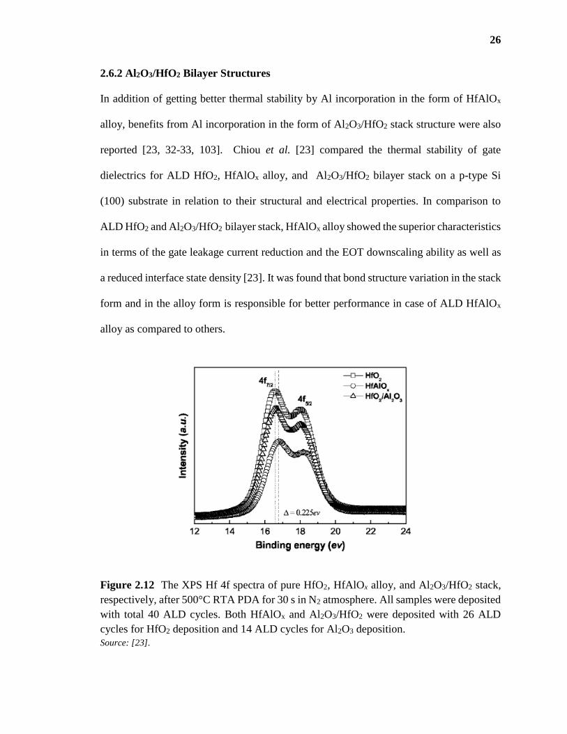
Figure 2.12 The XPS Hf 4f spectra of pure HfO2, HfAlOx alloy, and Al2O3/HfO2 stack,
respectively, after 500°C RTA PDA for 30 s in N2 atmosphere. All samples were deposited
with total 40 ALD cycles. Both HfAlOx and Al2O3/HfO2 were deposited with 26 ALD
cycles for HfO2 deposition and 14 ALD cycles for Al2O3 deposition.
Source: [23].
27
Figure 2.12 shows the XPS spectra of Hf 4f core levels [23]. The peak position of
Hf 4f in HfAlOx sample shifts to a higher binding energy compared to that in HfO2 and
Al2O3/HfO2 samples, which suggests the formation of a Hf-O-Al bond in the PDA HfAlOx
film [23], as Hf is more ionic than Al in the HfAlOx matrix [104]. Also, it was observed
that the HfO2 film began to crystallize around 600°C, but the HfO2 sub layer in the
Al2O3/HfO2 stack became crystallized around 700°C. The HfAlOx alloy on the other hand
remained amorphous even after a rapid thermal annealing (RTA) in N2 atmosphere at
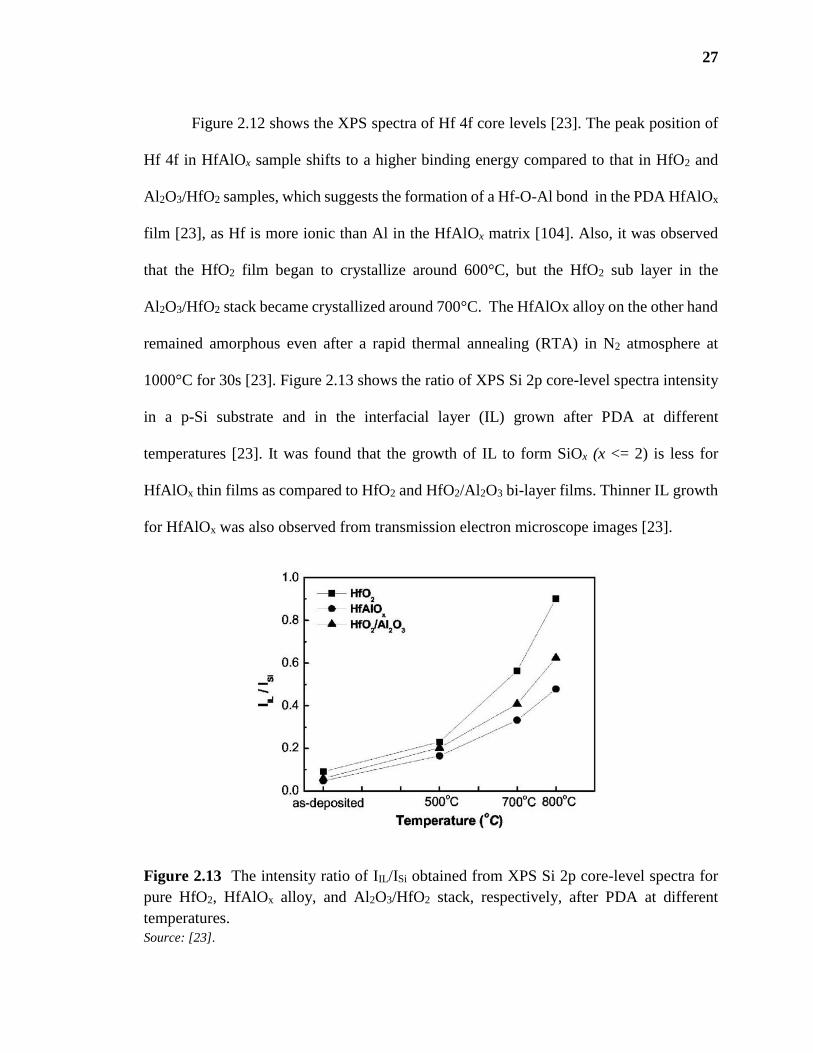
1000°C for 30s [23]. Figure 2.13 shows the ratio of XPS Si 2p core-level spectra intensity
in a p-Si substrate and in the interfacial layer (IL) grown after PDA at different
temperatures [23]. It was found that the growth of IL to form SiOx (x <= 2) is less for
HfAlOx thin films as compared to HfO2 and HfO2/Al2O3 bi-layer films. Thinner IL growth
for HfAlOx was also observed from transmission electron microscope images [23].
Figure 2.13 The intensity ratio of IIL/ISi obtained from XPS Si 2p core-level spectra for
pure HfO2, HfAlOx alloy, and Al2O3/HfO2 stack, respectively, after PDA at different
temperatures.
Source: [23].
28
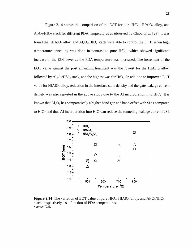
Figure 2.14 shows the comparison of the EOT for pure HfO2, HfAlOx alloy, and
Al2O3/HfO2 stack for different PDA temperatures as observed by Chiou et al. [23]. It was
found that HfAlOx alloy, and Al2O3/HfO2 stack were able to control the EOT, when high
temperature annealing was done in contrast to pure HfO2, which showed significant
increase in the EOT level as the PDA temperature was increased. The increment of the
EOT value against the post annealing treatment was the lowest for the HfAlOx alloy,
followed by Al2O3/HfO2 stack, and the highest was for HfO2. In addition to improved EOT
value for HfAlOx alloy, reduction in the interface state density and the gate leakage current
density was also reported in the above study due to the Al incorporation into HfO2. It is
known that Al2O3 has comparatively a higher band gap and band offset with Si as compared
to HfO2 and thus Al incorporation into HfO2can reduce the tunneling leakage current [23].
Figure 2.14 The variation of EOT value of pure HfO2, HfAlOx alloy, and Al2O3/HfO2
stack, respectively, as a function of PDA temperatures. Source: [23].
29
Figure 2.15 The variation of current density at VFB−1 volts as a function of PDA
temperatures for pure HfO2, HfAlOx alloy, and Al2O3/HfO2 stack on Si, respectively.
Source: [23].
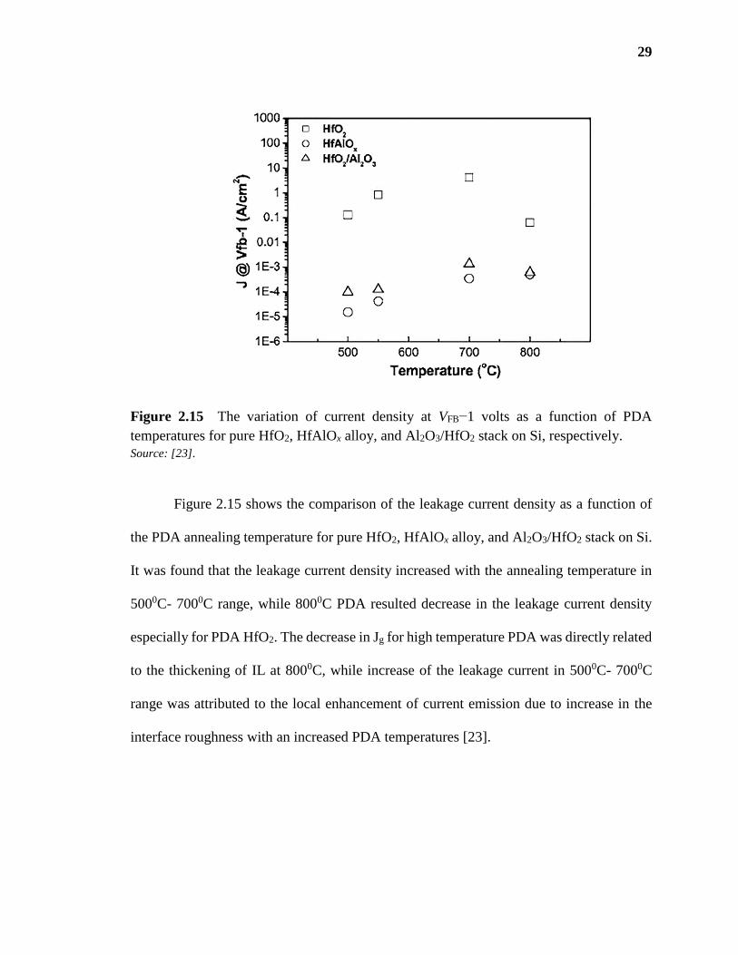
Figure 2.15 shows the comparison of the leakage current density as a function of
the PDA annealing temperature for pure HfO2, HfAlOx alloy, and Al2O3/HfO2 stack on Si.
It was found that the leakage current density increased with the annealing temperature in
5000C- 7000C range, while 8000C PDA resulted decrease in the leakage current density
especially for PDA HfO2. The decrease in Jg for high temperature PDA was directly related
to the thickening of IL at 8000C, while increase of the leakage current in 5000C- 7000C
range was attributed to the local enhancement of current emission due to increase in the
interface roughness with an increased PDA temperatures [23].
30
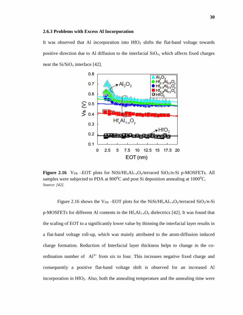
2.6.3 Problems with Excess Al Incorporation
It was observed that Al incorporation into HfO2 shifts the flat-band voltage towards
positive direction due to Al diffusion to the interfacial SiOx, which affects fixed charges
near the Si/SiOx interface [42].
Figure 2.16 VFB –EOT plots for NiSi/HfxAl1-xOy/terraced SiO2/n-Si p-MOSFETs. All
samples were subjected to PDA at 8000C and post Si deposition annealing at 10000C.
Source: [42].
Figure 2.16 shows the VFB –EOT plots for the NiSi/HfxAl1-xOy/terraced SiO2/n-Si
p-MOSFETs for different Al contents in the HfxAl1-xOy dielectrics [42]. It was found that
the scaling of EOT to a significantly lower value by thinning the interfacial layer results in
a flat-band voltage roll-up, which was mainly attributed to the atom-diffusion induced
charge formation. Reduction of Interfacial layer thickness helps to change in the co-
ordination number of Al3+ from six to four. This increases negative fixed charge and
consequently a positive flat-band voltage shift is observed for an increased Al
incorporation in HfO2. Also, both the annealing temperature and the annealing time were
31
found to have a significant effect on the charge formation in the dielectric because of the
Al diffusion [42]. In addition, more dipole formation in the high-/SiOx interface is also
reported for the Al incorporation into HfO2 [43-45], which contributes to a positive flat-
band voltage shift. However, the effect of Al incorporation into HfO2 on hole mobility was
found to be insignificant at both high and low effective field regions [42].
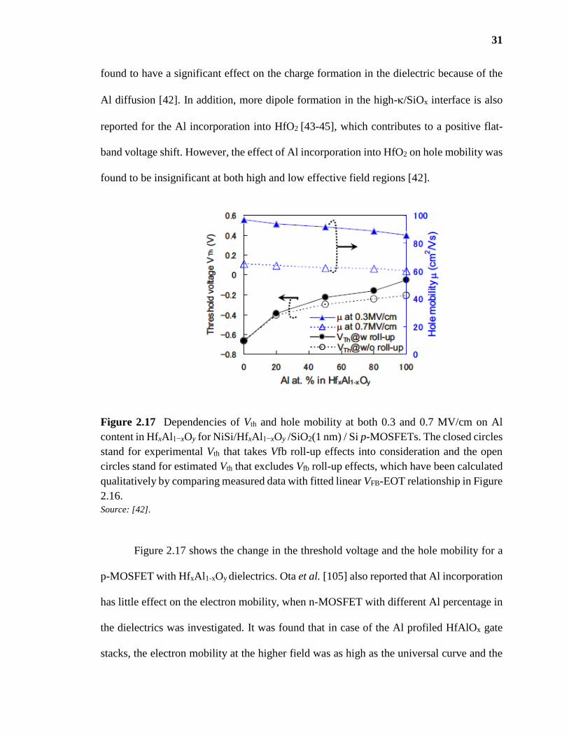
Figure 2.17 Dependencies of Vth and hole mobility at both 0.3 and 0.7 MV/cm on Al
content in HfxAl1−xOy for NiSi/HfxAl1−xOy /SiO2(1 nm) / Si p-MOSFETs. The closed circles
stand for experimental Vth that takes Vfb roll-up effects into consideration and the open
circles stand for estimated Vth that excludes Vfb roll-up effects, which have been calculated
qualitatively by comparing measured data with fitted linear VFB-EOT relationship in Figure
2.16.
Source: [42].
Figure 2.17 shows the change in the threshold voltage and the hole mobility for a
p-MOSFET with HfxAl1-xOy dielectrics. Ota et al. [105] also reported that Al incorporation
has little effect on the electron mobility, when n-MOSFET with different Al percentage in
the dielectrics was investigated. It was found that in case of the Al profiled HfAlOx gate
stacks, the electron mobility at the higher field was as high as the universal curve and the
32
influence of Al profiles on the electron mobility was restricted to the low effective field
region [105].
2.7 Chapter Summary
This chapter summarizes the recent advancements in Hf based high-dielectrics
processing conditions. The introduction of Zr into HfO2 was shown to be promising for
EOT downscaling. In addition various intermediate treatments during or after the ALD
deposition were found to be beneficial for the dielectric quality enhancement. HfAlOx
was also studied for different Hf to Al ratio in different structures, but they did not solve
reliability issues because of a higher Al percentage. An extremely low Al incorporation is
desirable to get good control on the device threshold voltage for highly scaled transistors.
Therefore, a systematic investigation of the electrical characteristics and the reliability for
these dielectrics is required.
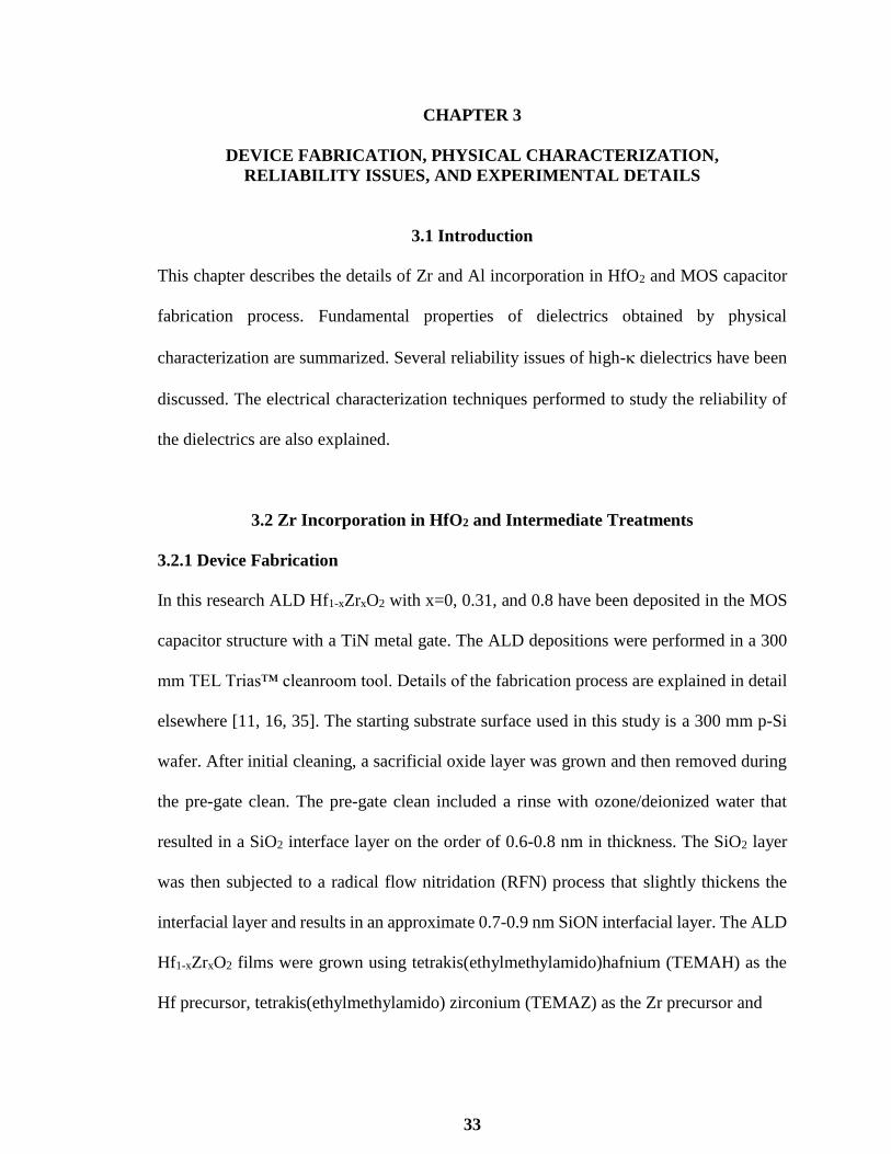
33
CHAPTER 3
DEVICE FABRICATION, PHYSICAL CHARACTERIZATION,
RELIABILITY ISSUES, AND EXPERIMENTAL DETAILS
3.1 Introduction
This chapter describes the details of Zr and Al incorporation in HfO2 and MOS capacitor
fabrication process. Fundamental properties of dielectrics obtained by physical
characterization are summarized. Several reliability issues of high- dielectrics have been
discussed. The electrical characterization techniques performed to study the reliability of
the dielectrics are also explained.
3.2 Zr Incorporation in HfO2 and Intermediate Treatments
3.2.1 Device Fabrication
In this research ALD Hf1-xZrxO2 with x=0, 0.31, and 0.8 have been deposited in the MOS
capacitor structure with a TiN metal gate. The ALD depositions were performed in a 300
mm TEL Trias™ cleanroom tool. Details of the fabrication process are explained in detail
elsewhere [11, 16, 35]. The starting substrate surface used in this study is a 300 mm p-Si
wafer. After initial cleaning, a sacrificial oxide layer was grown and then removed during
the pre-gate clean. The pre-gate clean included a rinse with ozone/deionized water that
resulted in a SiO2 interface layer on the order of 0.6-0.8 nm in thickness. The SiO2 layer
was then subjected to a radical flow nitridation (RFN) process that slightly thickens the
interfacial layer and results in an approximate 0.7-0.9 nm SiON interfacial layer. The ALD
Hf1-xZrxO2 films were grown using tetrakis(ethylmethylamido)hafnium (TEMAH) as the
Hf precursor, tetrakis(ethylmethylamido) zirconium (TEMAZ) as the Zr precursor and
34
H2O as the oxidant at a deposition temperature of 250°C. The Hf1-xZrxO2 films were
deposited by precisely controlling the individual HfO2 and ZrO2 ALD cycles contained
within each super-cycle of the overall ALD process. For ALD Hf1-xZrxO2 with x= 0.31, the
ratio of Hf precursor to Zr precursor was 3:1, while the ratio was 3: 1 for x = 0.8.
Experimental splits were performed by varying the intermediate treatment. Some samples
were subjected to a dielectric deposition and thermal annealing in a cyclical process called
DADA whereas some other samples were subjected to the same dielectric deposition and
exposure to Ar plasma in a SPA system [101] in a cyclical process called DSDS. The
dielectric in the control samples was deposited without any intermediate step (As-Dep).
Figure 3.1 (a) Device structure of TiN/Hf1-xZrxO2/SiON/p-Si MOSCAP, (b) dielectric
deposition with cyclic deposition and annealing (DADA) cyclic SPA plasma exposure
(DSDS).
Figure 3.1 shows the device structure with p-Si substrate, SiON interfacial layer,
ALD Hf1-xZrxO2, and TiN metal gate (Figure 3.1(a)) and high-Hf1-xZrxO2 deposition
1. ALD Hf1-xZrxO2 Deposition using TEMAH, TEMAZ and H2O at 250oC
(20/22cycles)
2. Anneal (N2 800oC for 40 s) OR Ar plasma in a SPA
system (40 s)
1. Deposition 2. Anneal/ SPA Ar Plasma
3. Repeat
(a) (b)
35
using intermediate treatments in a cyclical process (Figure 3.1(b)). For the DADA process
each deposition and anneal step consisted of a 20 ALD cycles of dielectric deposition
followed by a 40 s anneal such that total 40 ALD cycle films were deposited using two
deposition and anneal iterations. As-Dep samples did not undergo any annealing or
intermediate treatment. The annealing was done in a rapid thermal annealing (RTA)
chamber in a N2 ambient at 800°C attached to the same cluster tool platform as the
deposition chamber, thus allowing for in-situ anneal (via vacuum transfer). The DSDS
process was also performed in a similar in-situ fashion as the DADA process. DSDS and
As-Dep samples were prepared by using 44 ALD cycles. For DSDS Hf1-xZrxO2, samples
were subjected to an Ar plasma exposure in a SPA plasma system after every 22 ALD
cycles. Therefore they were deposited by two iterations of dielectric deposition (22 ALD
cycles) and SPA plasma exposure. In addition, DSDS Hf0.2Zr0.8O2 was deposited on two
different type of interfacial layers: (i) SiON formed by UV nitridation (RFN) of chemically
grown SiO2 and (ii) plasma oxynitride grown after removing chemically grown oxide. All
other dielectrics were deposited on the first type. After the high- gate oxide deposition,
the metal gate was formed by 50nm of CVD TiN at 5000C. The MOSCAPs were then
formed by depositing a hard mask, patterning and etching the MOSCAPs and cleaning and
stripping the hard mask.
3.2.2 Fundamental Properties of Hf1-xZrxO2 Deposited by Different Processing
HfO2 and ZrO2 showed identical growth rate (~0.7Å/cycle) at 2500C. Hf and Zr
composition for the different ALD films were measured by X-ray photoelectron
spectroscopy (XPS) by using Thermo Fisher Theta Probe™ XPS system. It was

36
determined from the XPS measurements that ALD Hf1-xZrxO2 deposited with Hf-precursor
to Zr-precursor ratio of 3:1 and 1:3 resulted in x=0.31 and x=0.8 respectively.
Figure 3.2 TEM images for (a) As-Dep HfO2, (b) DSDS HfO2, and (c) DSDS Hf0.2Zr0.8O2.
Figure 3.2 shows the Transmission Electron Micrograph (TEM) images for As-
Deposited HfO2 (Figure 3.2(a)), DSDS processed HfO2 (Figure 3.2(b)), and for DSDS
Hf0.2Zr0.8O2 (Figure 3.2(c)). Both DSDS and As-Deposited dielectrics were found to be
amorphous (Figure 3.2 (a-c)). For DADA Hf0.2Zr0.8O2, the structural characterization
showed stabilization into the tetragonal phase with a preferred (111) orientation, while
DADA HfO2 showed a monoclinic crystalline structure as shown in Figure 3.3 [35].
(a)
As-Dep HfO2
(b)
DSDS HfO2
(c)
DSDS Hf0.2Zr0.8O2
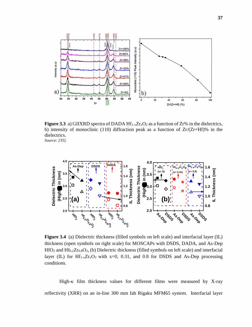
37
Figure 3.3 a) GIIXRD spectra of DADA Hf1-xZrxO2 as a function of Zr% in the dielectrics,
b) intensity of monoclinic (110) diffraction peak as a function of Zr/(Zr+Hf)% in the
dielectrics. Source: [35].
Figure 3.4 (a) Dielectric thickness (filled symbols on left scale) and interfacial layer (IL)
thickness (open symbols on right scale) for MOSCAPs with DSDS, DADA, and As-Dep
HfO2 and Hf0.2Zr0.8O2, (b) Dielectric thickness (filled symbols on left scale) and interfacial
layer (IL) for Hf1-xZrxO2 with x=0, 0.31, and 0.8 for DSDS and As-Dep processing
conditions.
High- film thickness values for different films were measured by X-ray
reflectivity (XRR) on an in-line 300 mm fab Rigaku MFM65 system. Interfacial layer
2.0
2.5
3.0
3.5
4.0
Hf0.2 Zr
0.8 O2
HfO
2
Hf0.2 Zr
0.8 O2
HfO
2
Hf0.2 Zr
0.8 O2
Die
lec
tric
Th
ick
ne
ss
(Hig
h-
) in
(n
m)
HfO
2
DSDSAs-Dep DADA
0.8
1.0
1.2
1.4
1.6
IL T
hic
kn
es
s (
nm
)
(a)
2.0
2.5
3.0
3.5
4.0
DSDS
DSDS
DSDS
As-D
ep
As-D
ep
Die
lec
tric
Th
ick
ne
ss
(H
igh
-)
in (
nm
)
As-D
ep
0.8
1.0
1.2
1.4
1.6Hf1-xZrxO2
(x= 0.31)
IL
Th
ickn
ess (
nm
)HfO2
(x= 0)
Hf1-xZrxO2
(x= 0.8)
(b)
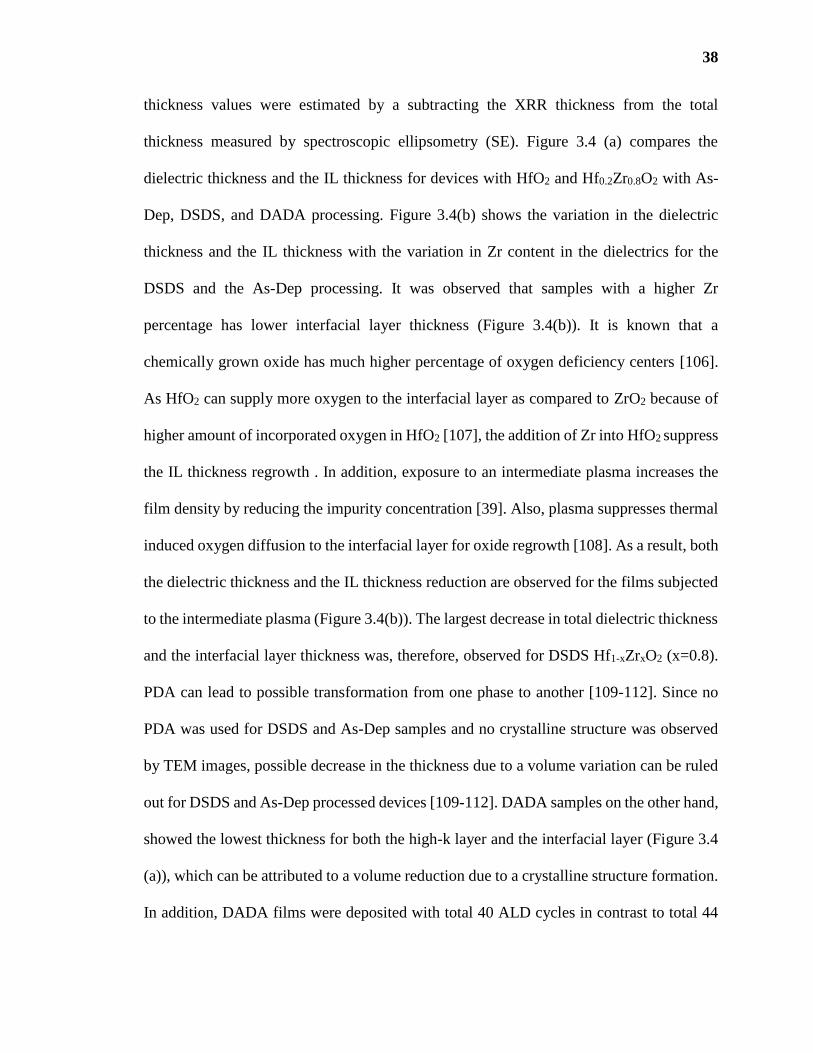
38
thickness values were estimated by a subtracting the XRR thickness from the total
thickness measured by spectroscopic ellipsometry (SE). Figure 3.4 (a) compares the
dielectric thickness and the IL thickness for devices with HfO2 and Hf0.2Zr0.8O2 with As-
Dep, DSDS, and DADA processing. Figure 3.4(b) shows the variation in the dielectric
thickness and the IL thickness with the variation in Zr content in the dielectrics for the
DSDS and the As-Dep processing. It was observed that samples with a higher Zr
percentage has lower interfacial layer thickness (Figure 3.4(b)). It is known that a
chemically grown oxide has much higher percentage of oxygen deficiency centers [106].
As HfO2 can supply more oxygen to the interfacial layer as compared to ZrO2 because of
higher amount of incorporated oxygen in HfO2 [107], the addition of Zr into HfO2 suppress
the IL thickness regrowth . In addition, exposure to an intermediate plasma increases the
film density by reducing the impurity concentration [39]. Also, plasma suppresses thermal
induced oxygen diffusion to the interfacial layer for oxide regrowth [108]. As a result, both
the dielectric thickness and the IL thickness reduction are observed for the films subjected
to the intermediate plasma (Figure 3.4(b)). The largest decrease in total dielectric thickness
and the interfacial layer thickness was, therefore, observed for DSDS Hf1-xZrxO2 (x=0.8).
PDA can lead to possible transformation from one phase to another [109-112]. Since no
PDA was used for DSDS and As-Dep samples and no crystalline structure was observed
by TEM images, possible decrease in the thickness due to a volume variation can be ruled
out for DSDS and As-Dep processed devices [109-112]. DADA samples on the other hand,
showed the lowest thickness for both the high-k layer and the interfacial layer (Figure 3.4
(a)), which can be attributed to a volume reduction due to a crystalline structure formation.
In addition, DADA films were deposited with total 40 ALD cycles in contrast to total 44
39
ALD cycles employed for DSDS and As-Dep dielectrics, which also contributes to a lower
dielectric thickness and IL thickness.
3.3 Extremely Low Al Incorporation in HfO2
3.3.1 Device Fabrication- ALD Multi Layered Structure
An Al doped HfO2 layer is incorporated in the gate stack of MOS capacitor with TiN metal
gate in two different lots, Lot A, and Lot B. The ALD depositions were conducted in a 300
mm TEL Trias™ cleanroom tool. The starting substrate surface used in this study is a 300
mm Si (001) wafer. The native oxide on the 300mm wafers was removed using a TEL
CertasTM chemical oxide removal (COR) process. The COR is a non-plasma dry cleaning
process. It utilizes a combination of anhydrous gaseous HF and NH3 rendering the surface
H terminated. A thin SiO2 interface layer (IL) was then formed using vapor ozone. ALD
HfO2 and HfAlOx was deposited by using tetrakis(ethylmethylamino)hafnium (TEMAH)
and trimethylaluminum (TMA) as Hf and Al precursors, respectively with H2O as the co-
reactant at 2500C deposition temperature. Details of the device fabrication will be found
elsewhere [34].
For Lot A the aluminum concentration was varied by depositing i) 30 ALD cycles
of HfO2 and 10 ALD cycles of HfAlOx (A1) , ii) 20 ALD cycles of HfO2 and 20 ALD
cycles of HfAlOx (A2) , and iii) 10 ALD cycles of HfO2 and 30 ALD cycles of HfAlOx
(A3). For Lot B the dielectrics were formed by depositing i) 10 ALD cycles of HfO2, 10
ALD cycles of HfAlOx, and 20 ALD cycles of HfO2 (B1), and ii) 10 ALD cycles of HfO2,
20 ALD cycles of HfAlOx and 10 ALD cycles of HfO2 (B2). A total of 40 cycles were used

40
for the entire deposition process for all the samples. The control sample in this study was
deposited with 40 ALD cycles of HfO2 (C).
Figure 3.5 (a) Device structure for Al incorporation in HfO2, (b) Device fabrication
process flow.
(a)
(b)
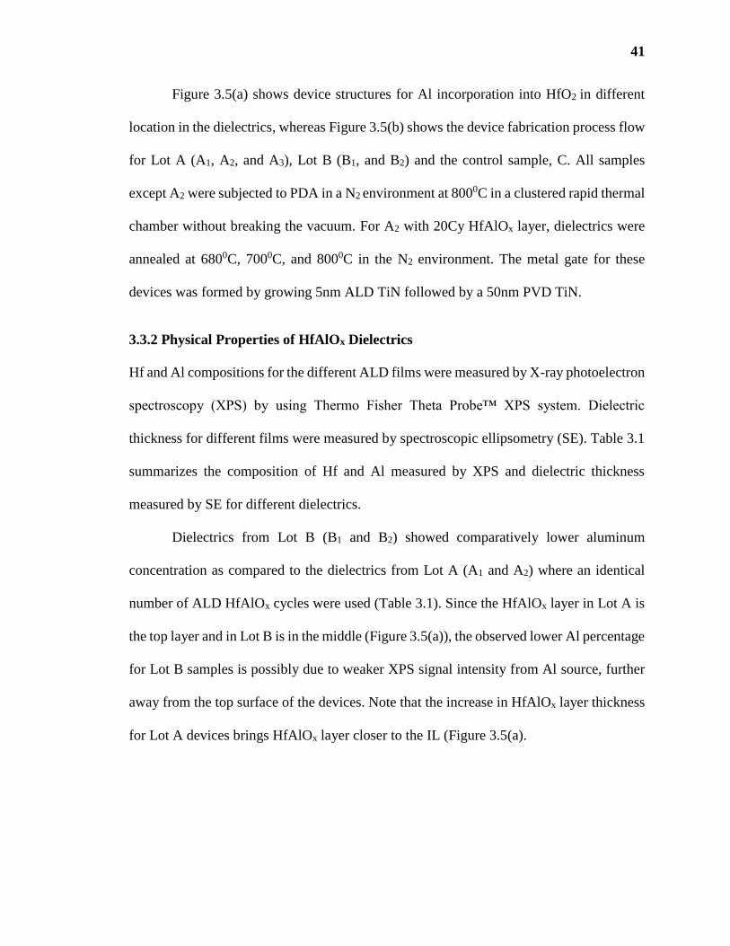
41
Figure 3.5(a) shows device structures for Al incorporation into HfO2 in different
location in the dielectrics, whereas Figure 3.5(b) shows the device fabrication process flow
for Lot A (A1, A2, and A3), Lot B (B1, and B2) and the control sample, C. All samples
except A2 were subjected to PDA in a N2 environment at 8000C in a clustered rapid thermal
chamber without breaking the vacuum. For A2 with 20Cy HfAlOx layer, dielectrics were
annealed at 6800C, 7000C, and 8000C in the N2 environment. The metal gate for these
devices was formed by growing 5nm ALD TiN followed by a 50nm PVD TiN.
3.3.2 Physical Properties of HfAlOx Dielectrics
Hf and Al compositions for the different ALD films were measured by X-ray photoelectron
spectroscopy (XPS) by using Thermo Fisher Theta Probe™ XPS system. Dielectric
thickness for different films were measured by spectroscopic ellipsometry (SE). Table 3.1
summarizes the composition of Hf and Al measured by XPS and dielectric thickness
measured by SE for different dielectrics.
Dielectrics from Lot B (B1 and B2) showed comparatively lower aluminum
concentration as compared to the dielectrics from Lot A (A1 and A2) where an identical
number of ALD HfAlOx cycles were used (Table 3.1). Since the HfAlOx layer in Lot A is
the top layer and in Lot B is in the middle (Figure 3.5(a)), the observed lower Al percentage
for Lot B samples is possibly due to weaker XPS signal intensity from Al source, further
away from the top surface of the devices. Note that the increase in HfAlOx layer thickness
for Lot A devices brings HfAlOx layer closer to the IL (Figure 3.5(a).
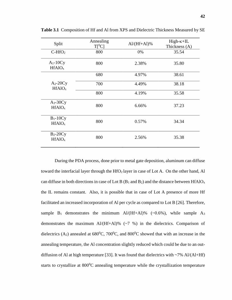
42
Table 3.1 Composition of Hf and Al from XPS and Dielectric Thickness Measured by SE
During the PDA process, done prior to metal gate deposition, aluminum can diffuse
toward the interfacial layer through the HfO2 layer in case of Lot A. On the other hand, Al
can diffuse in both directions in case of Lot B (B1 and B2) and the distance between HfAlOx
the IL remains constant. Also, it is possible that in case of Lot A presence of more Hf
facilitated an increased incorporation of Al per cycle as compared to Lot B [26]. Therefore,
sample B1 demonstrates the minimum Al/(Hf+Al)% (~0.6%), while sample A3
demonstrates the maximum Al/(Hf+Al)% (~7 %) in the dielectrics. Comparison of
dielectrics (A2) annealed at 6800C, 7000C, and 8000C showed that with an increase in the
annealing temperature, the Al concentration slightly reduced which could be due to an out-
diffusion of Al at high temperature [33]. It was found that dielectrics with ~7% Al/(Al+Hf)
starts to crystallize at 8000C annealing temperature while the crystallization temperature
Split Annealing
T[0C] Al/(Hf+Al)%
High-+IL
Thickness (A)
C-HfO2 800 0% 35.54
A1-10Cy
HfAlOx 800 2.38% 35.80
A2-20Cy
HfAlOx
680 4.97% 38.61
700 4.49% 38.18
800 4.19% 35.58
A3-30Cy
HfAlOx
800 6.66% 37.23
B1-10Cy
HfAlOx
800 0.57% 34.34
B2-20Cy
HfAlOx
800 2.56% 35.38

43
decreases for dielectrics with lower Al percentage [34]. Therefore, A3 with a 30 cy HfAlOx
showed ~2Å higher film thickness because of a mixed structure of amorphous and
crystalline phase formation as compared to other dielectrics (Table 3.1). When dielectrics
have 4-5% Al, they remain amorphous even after annealing at 7000C [34]. Therefore, A2
with 20 Cy HfAlOx annealed at 6800C, and 7000C showed ~3Å higher thickness as
compared to the dielectric annealed at 8000C (Table 3.1). B1 having the lowest Al
percentage showed the lowest dielectric thickness (Table 3.1).
3.4 Defects and Reliability of High-Dielectrics
The introduction of high- dielectric materials paved the way for device scaling below 1
nm with a significant reduction in the leakage current due to direct tunneling, as formation
of a thicker oxide is possible for the same EOT value as compared to SiO2. The problem
with high-dielectric materials arises from their large intrinsic defect density, which is
responsible for charge trapping and degradation of the gate stack. Also, formation of fixed
charge causes carrier scattering in the Si-substrate. Moreover, as defects or their charge
states evolve in time, dielectric properties and device performance can vary even from one
region to another over a wafer [113]. Although ALD process can provide better film
deposition with precise control of thickness, ALD grown oxide films suffer from a high
leakage current, a high trap density, and comparatively lower reliability because of the
large number of defects in the films introduced by impurities in the precursor gases
especially at low temperatures [47-48, 114-116].
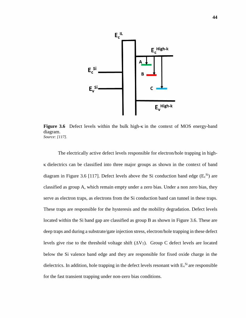
44
Figure 3.6 Defect levels within the bulk high-in the context of MOS energy-band
diagram. Source: [117].
The electrically active defect levels responsible for electron/hole trapping in high-
dielectrics can be classified into three major groups as shown in the context of band
diagram in Figure 3.6 [117]. Defect levels above the Si conduction band edge (EcSi) are
classified as group A, which remain empty under a zero bias. Under a non zero bias, they
serve as electron traps, as electrons from the Si conduction band can tunnel in these traps.
These traps are responsible for the hysteresis and the mobility degradation. Defect levels
located within the Si band gap are classified as group B as shown in Figure 3.6. These are
deep traps and during a substrate/gate injection stress, electron/hole trapping in these defect
levels give rise to the threshold voltage shift (VT). Group C defect levels are located
below the Si valence band edge and they are responsible for fixed oxide charge in the
dielectrics. In addition, hole trapping in the defect levels resonant with EvSi
are responsible
for the fast transient trapping under non-zero bias conditions.

45
3.4.1 Constant Voltage Stress Induced Degradations
Typically, the reliability of the high- gate stacks is studied by applying a constant voltage
stress. Experimental observation of the charge trapping in high- gate oxides under
different stress conditions is widely reported [46-49, 118-124]. Stress induced flat-band
voltage shifts [52] and stress-induced leakage currents (SILC) were also observed [53-54].
In addition, the reliability of high- gate dielectric is influenced by the reliability of both
the interfacial layer and the high- layer. It was also observed that the Hf-based high-
layer modifies the underlying interfacial SiO2 layer by rendering it oxygen deficient [65].
The quality of the IL also affects the mobility of long channel nFETs [55]. A brief
description of different degradation mechanisms and their impact on the reliability are
mentioned below.
3.4.1.1 Stress Induced Flat-band Voltage Shift (VFB). Stress voltage can be applied
in the gate injection mode (negative voltage to the gate) or in the substrate injection mode
(positive voltage to the metal gate). Under substrate injection mode, electrons tunnel from
the substrate through the gate dielectrics and cause a negative charge trapping in the
dielectrics, while under gate injection mode, electrons tunnel from the gate through the
dielectrics to the substrate and cause a positive charge formation in the dielectrics [69].
Stress in the substrate injection mode is unsuitable for MOS capacitor with a p-Si substrate,
as the substrate cannot provide sufficient electron. When devices are stressed in the gate
injection mode, positive charge generation in the dielectrics by holes from the substrate or
by hydrogen related species released from the anode interface causes a negative flat-band
voltage shift [52-53]. Also, stress induced interface state generation contributes to the flat-

46
band voltage shift [60-61]. The detrimental effects of the stress induced flat-band voltage
shift are an increased threshold voltage (VT), an absolute off current (Ioff) increase, an
absolute drain current (IDsat) reduction, and a transconductance (gm) decrease.
Figure 3.7 (a) Band diagram showing positive charge formation in the dielectric under
stress in the gate injection mode, (b) Capacitance–voltage characteristics of p-Si/SiO2
/ZrO2 /TiN structures measured before and after constant gate voltage stress at -3.6 V for
400 s. Solid lines are fits to the data using a computer simulation. Inset: Energetic
distribution of interface defects used for simulation of the C–V characteristics.
Source: [125].
Figure 3.7 (a) shows the mechanism of positive charge formation under the stress
in the gate injection mode, and Figure 3.7(b) shows a typical capacitance voltage
characteristics for a device with high-dielectric and SiO2 interfacial layer before and after
the application of a constant voltage stress in the gate injection mode [125]. Stress induced
positive charge formation contributes to the threshold voltage shift in these devices [55].
3.4.1.2 Stress Induced Leakage Current (SILC). In addition to a positive charge
formation in the dielectrics, applied stress voltage causes an increase in the gate leakage
Metal
Gate
High-
Layer
Interfacial
Layer
p-Si Substrate
(a)
(b)

47
current known as stress induced leakage current (SILC). It was found that a composite
effect of neutral trap generation, electron trapping, and positive charge generation
contributes to the variation in C-V and I-V characteristics after the stress [52-55]. However,
SILC is found to be a reliability issue at high stress voltages [54]. Therefore, in applications
where high voltage are required for normal operations such as non-volatile memories,
replacement of HfO2 can pose severe reliability issue due to a large leakage current if SILC
cannot be minimized.
J. Maserijian [126] first observed that the device stressed under a high field had
increased leakage current, when the current was measured in the low applied field region,
which is usually known as the direct tunneling (DT) region. According to D. J. DiMaria et
al. [127], stress induced leakage current in the direct tunneling is due to the deterioration
of the oxide film and a positive charge formation. On the other hand, Rofan et al. [128]
found that the generation of interface states is responsible for the increased leakage current
as a result of stress, while according to Dumin et al. [129] the bulk oxide electron trap
generation is responsible for the stress induced leakage current (SILC). SILC is defined as
J(t)= J(t) – J(0), i. e., the difference in leakage current density after stressing for a certain
period t. The normalized SILC is defined by J(t)/ J(0) and is proportional to the density
of traps generated by stress [127].
It was found that, SILC depends on the stress voltage as well as the sense voltage
[130]. Figure 3.8 shows the conduction mechanism through the high-layer and the
interfacial layer in the positive gate bias condition (Figure 3.8(a)) and in the negative gate
bias condition (Figure 3.8(b)).
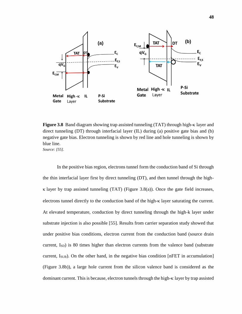
48
Figure 3.8 Band diagram showing trap assisted tunneling (TAT) through high-layer and
direct tunneling (DT) through interfacial layer (IL) during (a) positive gate bias and (b)
negative gate bias. Electron tunneling is shown by red line and hole tunneling is shown by
blue line.
Source: [55].
In the positive bias region, electrons tunnel form the conduction band of Si through
the thin interfacial layer first by direct tunneling (DT), and then tunnel through the high-
layer by trap assisted tunneling (TAT) (Figure 3.8(a)). Once the gate field increases,
electrons tunnel directly to the conduction band of the high-layer saturating the current.
At elevated temperature, conduction by direct tunneling through the high-k layer under
substrate injection is also possible [55]. Results from carrier separation study showed that
under positive bias conditions, electron current from the conduction band (source drain
current, ISD) is 80 times higher than electron currents from the valence band (substrate
current, ISUB). On the other hand, in the negative bias condition [nFET in accumulation]
(Figure 3.8b)), a large hole current from the silicon valence band is considered as the
dominant current. This is because, electron tunnels through the high-layer by trap assisted
(a) (b)

49
tunneling and then goes to the conduction band of Si by direct tunneling. Whereas, holes
from the valence band move ~5 times faster through the tunneling barrier of the interfacial
layer [55].
3.4.1.3 Stress Induced Interface State Generation (Dit). Under the electrical stress,
interface state generation by the hole injection and the hole trapping at and near Si/SiO2 or
Si/SiON interface is a reliability concern for HfO2 based dielectrics [55]. Increase in the
Dit causes the threshold voltage (VT) shift, the reduced transconductance (gm), and the
increased subthreshold slope [70]. With a variation in high-dielectric material and
processing condition, the interfacial layer thickness and the interface roughness varies [71].
Therefore, it is expected that Dit generation with the stress has a significant contribution on
the long term reliability of these dielectrics. Conductance method offers the advantage of
determining the Dit directly from the experiment, as compared to other C-V based methods
[72-73]. However, a correct Dit extraction by this method requires an efficient Fermi level
movement [73].
3.4.2 Time Dependent Dielectric Breakdown (TDDB)
Defect generation in both the high- layer and the interfacial layer contributes to failure of
the dielectric stack [74]. During the constant voltage stress a critical density of generated
traps lead to the dielectric breakdown [75]. Also, the TDDB breakdown is a stochastic
process and strongly depends on the thickness of the high-layer and the interfacial layer
[76]. Furthermore, in case of the time dependent breakdown for a dielectric stack with a
high- layer and an interfacial layer, the interfacial layer initiates the breakdown process
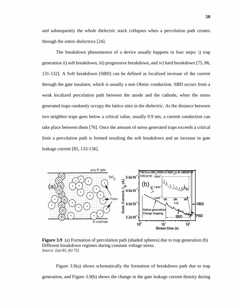
50
and subsequently the whole dielectric stack collapses when a percolation path creates
through the entire dielectrics [24].
The breakdown phenomenon of a device usually happens in four steps: i) trap
generation ii) soft breakdown, iii) progressive breakdown, and iv) hard breakdown [75, 86,
131-132]. A Soft breakdown (SBD) can be defined as localized increase of the current
through the gate insulator, which is usually a non Ohmic conduction. SBD occurs from a
weak localized percolation path between the anode and the cathode, when the stress
generated traps randomly occupy the lattice sites in the dielectric. As the distance between
two neighbor traps goes below a critical value, usually 0.9 nm, a current conduction can
take place between them [76]. Once the amount of stress generated traps exceeds a critical
limit a percolation path is formed resulting the soft breakdown and an increase in gate
leakage current [85, 133-136].
Figure 3.9 (a) Formation of percolation path (shaded spheres) due to trap generation (b)
Different breakdown regimes during constant voltage stress. Source: [(a) 85, (b) 75].
Figure 3.9(a) shows schematically the formation of breakdown path due to trap
generation, and Figure 3.9(b) shows the change in the gate leakage current density during
(a) (b)

51
the soft breakdown and the hard breakdown of a typical TiN/HfO2/ISSG IL (SiO2)/Si gate
stack [75]. According to S. Bruyere et al. [137] soft breakdown (SBD) and hard breakdown
(HBD) are localized and randomly distributed over the device area. As a result, the leakage
current fluctuates after the first soft breakdown due to trapping and de-trapping of electrons
in the percolation cluster and makes the dielectric noisy. After the SBD, continuous
degradation due to further stress leads to a catastrophic breakdown known as the hard break
down (HBD). In the progressive breakdown (PBD) regime the leakage current increases
sharply, but the noisy pattern of the leakage current still dominates as shown in Figure
3.9(b). The PBD is an outcome of the aging of the percolation path after the SBD.
Following the PBD, an immediate thermal runway can be seen, which drives the entire gate
stack to permanent failure termed as HBD [75]. The HBD and the SBD do not necessarily
occur at the same spatial location [138-139], rather they can play independently with
applied stress. Usually one can expect, the HBD occurring after a long time of the SBD, if
the stress voltage is low. To get the projected life time of a device, several techniques are
described in the literature. According to the model proposed by the prevalence method
[139-141], the HBD distribution is shifted from the first SBD time by a factor, which
depends on the stress conditions. The successive breakdown method [141] provides
another methodology to find the failure time depending on the limit of gate leakage current.
As described earlier, defects in the dielectric introduces variation in the
characteristics of devices, and consequently the time to breakdown is a random variable
and the distribution of TBD follows the Weibull statistics. The cumulative distribution
failure (CDF) for the Weibull distribution is:

52
𝐹(𝑡) = 1 − exp(−(𝑡
𝜂)𝛽 ) (3.1)
Here β is the shape parameter or the Weibull slope and η is the scale parameter or the
characteristic life time. According to Degraeve [85], the Weibull slope β of the break down
for a dielectric is strongly dependent on the thickness of the dielectric.
Figure 3.10 Dependence of the Weibull slope β of the charge to breakdown, QBD on the
oxide thickness.
Source: [85].
Figure 3.10 shows the dependence of β on the thickness of the dielectric for a single
radius of trap r= 0.45 nm for a Polysilicon/SiO2 gate stack. According to Degrave et al.
[85] thinner oxides require few traps to form a conductive breakdown path and
consequently they have a lower value of β due to a larger statistical spread on the average

53
density to form such a conductive path as compared to thicker oxides. As the dielectric
thickness and the interfacial layer thickness vary with the deposition process of high-
dielectric, the Weibull slope β can provide significant information about the effect of
different processing on the device characteristics and performance.
For various applications (such as memory application), it is possible that the
operating voltage will be much higher to degrade the gate stack quality. Understanding the
impact of Zr or Al addition in HfO2 on the reliability is a prerequisite to integrate these
dielectrics in future CMOS technologies. Also the impact of intermediate treatments such
as the cyclic annealing and the cyclic SPA plasma treatment on the reliability is necessary.
Understanding the above mentioned degradation mechanisms (VFB, SILC, Dit and
TDDB) is a fundamental to allow the accurate reliability prediction for these dielectrics.
3.5 Electrical Characterization and Reliability Study
In order to design and fabricate high performance devices with improved reliability,
measurement of electrical properties, parameters extracted from these measurements and
control over these parameters are highly important. For stable performance of a MOS
device, charges in the bulk oxide and oxide-substrate interface are undesirable. These
charges adversely affect the performance and the reliability of transistors with high-
dielectrics. MOS capacitors were used for the characterization and the reliability study
because of the simplicity in fabrication and analysis they offer. Following measurement
techniques have been employed for the characterization and the reliability study of Zr and
Al incorporated HfO2.
54
3.5.1 Capacitance-Voltage (C-V) Measurement
Capacitance voltage (C-V) measurement were carried out by using an Agilent 4284A LCR
meter. The EOT and the flat-band voltage have been calculated from C-V characteristics
by using the NCSU CVC program [142]. MOS capacitors with 40 m × 40 m gate area
have been characterized in a Cascade Microchamber with precision probe station. High
frequency (HF) C-V characteristics at 250 KHz for different dielectrics were analyzed for
the EOT and the flat-band voltage comparison.
3.5.2 Conductance Measurement
Several techniques are available in the literature for estimating the interface trap density,
Dit [143]. The conductance method, proposed by Nicollian and Goetzberger in 1967 [144],
yields the Dit in the depletion and weak inversion portion of the band gap, by measuring
the equivalent parallel conductance of a MOSCAP as a function of the bias voltage and the
frequency. The interface traps are detected through the loss resulting from changes in their
occupancy due to changes in the gate voltage during the ac measurement [143].
Conductance method offers the advantage of determining the Dit directly from the
experiment, as compared to other C-V based methods [72-73]. Also, with the gate bias
change, the efficiency of the band bending and the Fermi level movement can be observed
from the shift of the normalized conductance peak as a function of the frequency [72]. In
this research, we used a 4284A LCR meter for Cm-Vg and Gm-Vg measurements using the
parallel Cp-Gp model at room temperature in a Cascade Micro chamber with precision
probe station. The dc gate voltage was varied from 1V to -2V with -20 mV voltage step
and measurement frequencies used in this work were in the range of 1MHz to 100 Hz. The
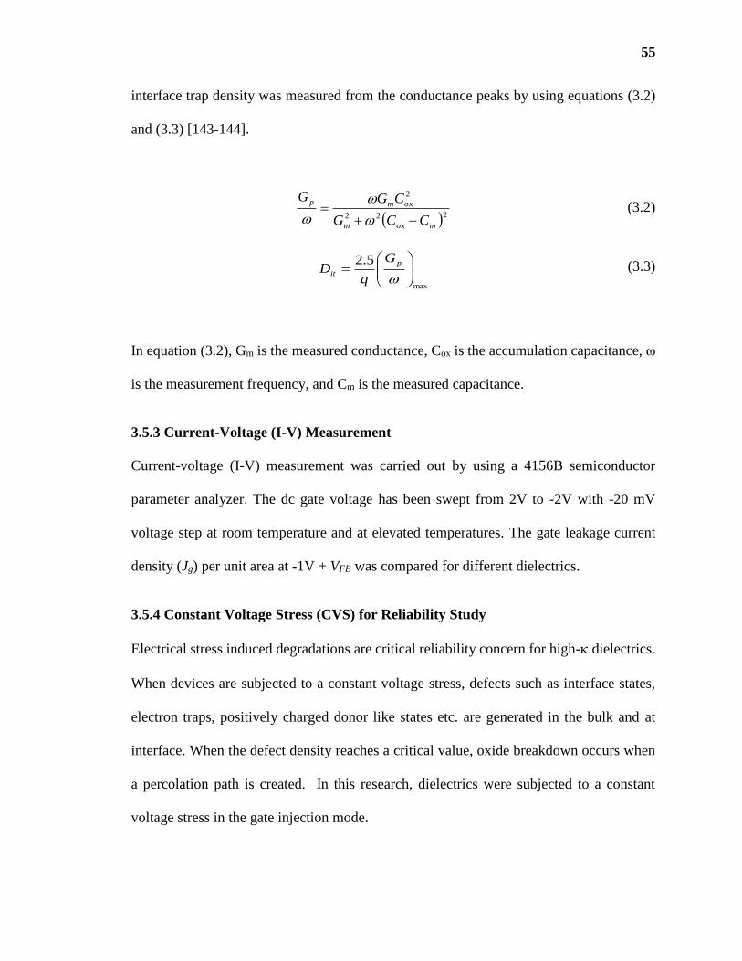
55
interface trap density was measured from the conductance peaks by using equations (3.2)
and (3.3) [143-144].
222
2
moxm
oxmp
CCG
CGG
(3.2)
max
5.2
p
it
G
qD (3.3)
In equation (3.2), Gm is the measured conductance, Cox is the accumulation capacitance, ω
is the measurement frequency, and Cm is the measured capacitance.
3.5.3 Current-Voltage (I-V) Measurement
Current-voltage (I-V) measurement was carried out by using a 4156B semiconductor
parameter analyzer. The dc gate voltage has been swept from 2V to -2V with -20 mV
voltage step at room temperature and at elevated temperatures. The gate leakage current
density (Jg) per unit area at -1V + VFB was compared for different dielectrics.
3.5.4 Constant Voltage Stress (CVS) for Reliability Study
Electrical stress induced degradations are critical reliability concern for high-dielectrics.
When devices are subjected to a constant voltage stress, defects such as interface states,
electron traps, positively charged donor like states etc. are generated in the bulk and at
interface. When the defect density reaches a critical value, oxide breakdown occurs when
a percolation path is created. In this research, dielectrics were subjected to a constant
voltage stress in the gate injection mode.
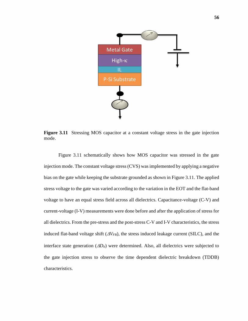
56
Figure 3.11 Stressing MOS capacitor at a constant voltage stress in the gate injection
mode.
Figure 3.11 schematically shows how MOS capacitor was stressed in the gate
injection mode. The constant voltage stress (CVS) was implemented by applying a negative
bias on the gate while keeping the substrate grounded as shown in Figure 3.11. The applied
stress voltage to the gate was varied according to the variation in the EOT and the flat-band
voltage to have an equal stress field across all dielectrics. Capacitance-voltage (C-V) and
current-voltage (I-V) measurements were done before and after the application of stress for
all dielectrics. From the pre-stress and the post-stress C-V and I-V characteristics, the stress
induced flat-band voltage shift (VFB), the stress induced leakage current (SILC), and the
interface state generation (Dit) were determined. Also, all dielectrics were subjected to
the gate injection stress to observe the time dependent dielectric breakdown (TDDB)
characteristics.
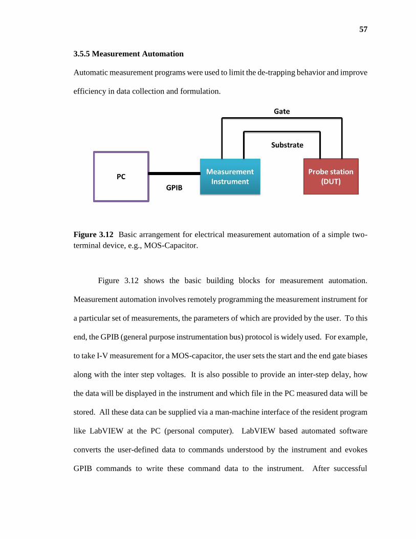
57
3.5.5 Measurement Automation
Automatic measurement programs were used to limit the de-trapping behavior and improve
efficiency in data collection and formulation.
Figure 3.12 Basic arrangement for electrical measurement automation of a simple two-
terminal device, e.g., MOS-Capacitor.
Figure 3.12 shows the basic building blocks for measurement automation.
Measurement automation involves remotely programming the measurement instrument for
a particular set of measurements, the parameters of which are provided by the user. To this
end, the GPIB (general purpose instrumentation bus) protocol is widely used. For example,
to take I-V measurement for a MOS-capacitor, the user sets the start and the end gate biases
along with the inter step voltages. It is also possible to provide an inter-step delay, how
the data will be displayed in the instrument and which file in the PC measured data will be
stored. All these data can be supplied via a man-machine interface of the resident program
like LabVIEW at the PC (personal computer). LabVIEW based automated software
converts the user-defined data to commands understood by the instrument and evokes
GPIB commands to write these command data to the instrument. After successful
58
transmission of the command data to the instrument, it triggers the instrument to run the
measurement. After the completion of the measurement, the automation software stores a
copy of the data at the instrument. It opens the file again and evokes it to transmit back to
the PC and store them in a user- defined file.
3.6 Chapter Summary
This chapter summarizes the fabrication process of MOS capacitors with Zr and Al
incorporated HfO2 used in this study. Details of the physical characterization has been
discussed. A brief discussion of different defects in Hf-based high-k dielectrics is presented
and different stress induced degradation mechanisms are explained. Also, all electrical
measurement and reliability study techniques used in this thesis were discussed.
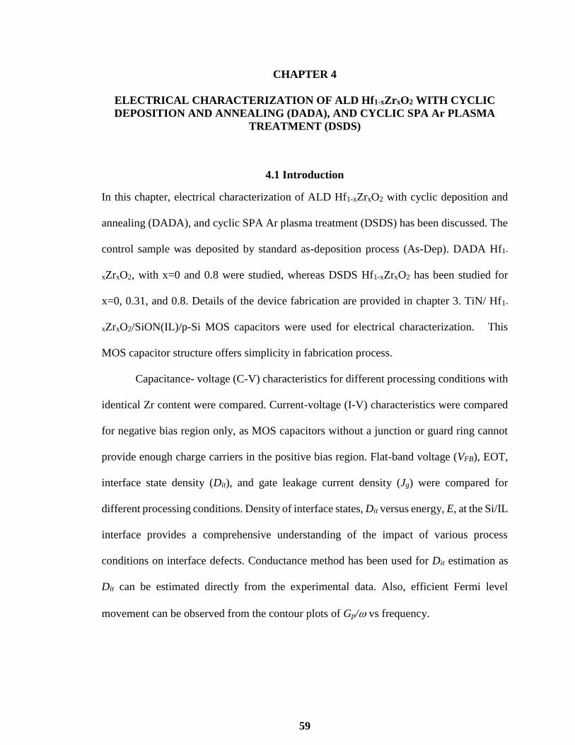
59
CHAPTER 4
ELECTRICAL CHARACTERIZATION OF ALD Hf1-xZrxO2 WITH CYCLIC
DEPOSITION AND ANNEALING (DADA), AND CYCLIC SPA Ar PLASMA
TREATMENT (DSDS)
4.1 Introduction
In this chapter, electrical characterization of ALD Hf1-xZrxO2 with cyclic deposition and
annealing (DADA), and cyclic SPA Ar plasma treatment (DSDS) has been discussed. The
control sample was deposited by standard as-deposition process (As-Dep). DADA Hf1-
xZrxO2, with x=0 and 0.8 were studied, whereas DSDS Hf1-xZrxO2 has been studied for
x=0, 0.31, and 0.8. Details of the device fabrication are provided in chapter 3. TiN/ Hf1-
xZrxO2/SiON(IL)/p-Si MOS capacitors were used for electrical characterization. This
MOS capacitor structure offers simplicity in fabrication process.
Capacitance- voltage (C-V) characteristics for different processing conditions with
identical Zr content were compared. Current-voltage (I-V) characteristics were compared
for negative bias region only, as MOS capacitors without a junction or guard ring cannot
provide enough charge carriers in the positive bias region. Flat-band voltage (VFB), EOT,
interface state density (Dit), and gate leakage current density (Jg) were compared for
different processing conditions. Density of interface states, Dit versus energy, E, at the Si/IL
interface provides a comprehensive understanding of the impact of various process
conditions on interface defects. Conductance method has been used for Dit estimation as
Dit can be estimated directly from the experimental data. Also, efficient Fermi level
movement can be observed from the contour plots of Gp/vs frequency.
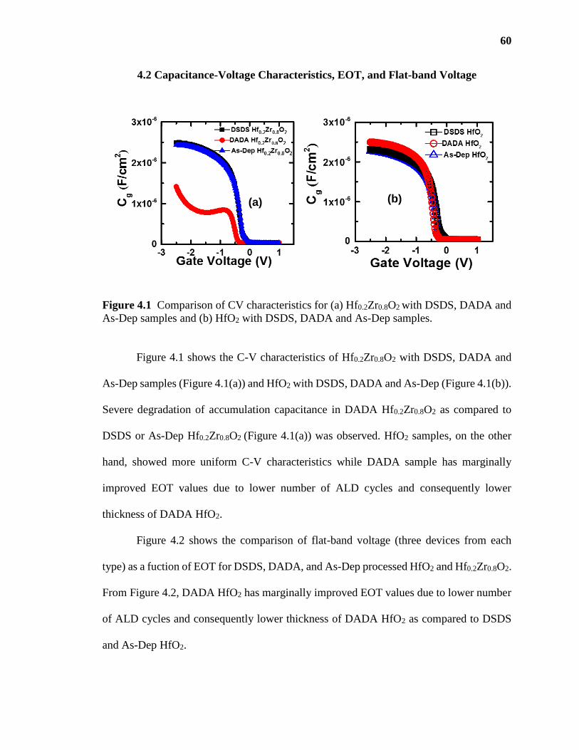
60
4.2 Capacitance-Voltage Characteristics, EOT, and Flat-band Voltage
Figure 4.1 Comparison of CV characteristics for (a) Hf0.2Zr0.8O2 with DSDS, DADA and
As-Dep samples and (b) HfO2 with DSDS, DADA and As-Dep samples.
Figure 4.1 shows the C-V characteristics of Hf0.2Zr0.8O2 with DSDS, DADA and
As-Dep samples (Figure 4.1(a)) and HfO2 with DSDS, DADA and As-Dep (Figure 4.1(b)).
Severe degradation of accumulation capacitance in DADA Hf0.2Zr0.8O2 as compared to
DSDS or As-Dep Hf0.2Zr0.8O2 (Figure 4.1(a)) was observed. HfO2 samples, on the other
hand, showed more uniform C-V characteristics while DADA sample has marginally
improved EOT values due to lower number of ALD cycles and consequently lower
thickness of DADA HfO2.
Figure 4.2 shows the comparison of flat-band voltage (three devices from each
type) as a fuction of EOT for DSDS, DADA, and As-Dep processed HfO2 and Hf0.2Zr0.8O2.
From Figure 4.2, DADA HfO2 has marginally improved EOT values due to lower number
of ALD cycles and consequently lower thickness of DADA HfO2 as compared to DSDS
and As-Dep HfO2.
(a) (b)
61
Figure 4.2 Flat-band voltage VFB, as a function of EOT for Hf0.2Zr0.8O2 and HfO2 with
DSDS, DADA, and As-Dep processing.
An EOT reduction as a result of the ZrO2 addition was observed for the DSDS and
for the As-Dep gate oxide while a significant reduction in the oxide capacitance (EOT
increased) and in the flatband shift was observed in DADA Hf0.2Zr0.8O2 (Figure 4.2). The
addition of Zr was found to reduce the interfacial layer thickness (Figure 3.4). It is known
that a chemically grown oxide (IL) has much higher percentage of oxygen deficiency
centers [107], and also HfO2 can supply more oxygen to the interfacial layer as compared
to Hf1-xZrxO2 because of a higher amount of incorporated oxygen in HfO2 [108]. Therefore,
the addition of Zr into HfO2 showed an EOT downscaling potential for the DSDS and the
As-Dep gate oxide by controlling the interfacial layer regrowth (Figure 4.2) [71]. Also,
amorphous ZrO2 has a higher value compared to amorphous HfO2 [3], which contributes
to lower EOT for the DSDS and the As-Dep Hf0.2Zr0.8O2. DADA samples with the addition
of Zr reveal that the intermediate annealing process degrades the performance of
Hf0.2Zr0.8O2 possibly forming a charged deformed interfacial layer that decreases the total
62
charge in the accumulation layer thereby reducing the accumulation capacitance (Figure
4.1(a)). It was reported earlier in Ref. 11 that a 10 percent reduction in the EOT was
observed for the DADA processed HfO2 as compared to the As-Dep HfO2 because of an
improved film densification and a reduction in carbon along with Si intermixing. In this
work EOT is 2.53 times higher (Figure 4.2) for DADA Hf0.2Zr0.8O2 as compared to DADA
HfO2 . It is possible that the intermixing at the interface is more detrimental for high
temperature treatment with high ZrO2 content than for the same treatment applied to HfO2.
The DSDS Hf0.2Zr0.8O2 film, on the other hand, did not go through any additional thermal
cycle leading to such degradation process with the additon of ZrO2 and showed a
comparable characteristics with DSDS HfO2 (Figure 4.1(a) and Figure 4.2). Also devices
with Hf0.2Zr0.8O2 showed a slightly higher flat-band voltage (VFB) as compared to devices
with HfO2 (Figure 4.2). It is known that ZrO2 has comparatively lower electron affinity
than HfO2 [145]. This results in a more positive charge formation in the dielectrics for
devices with Hf0.2Zr0.8O2. While the DSDS HfO2 and the As-Dep HfO2 showed a
comparable flat-band voltage, the DADA HfO2 on the other hand, showed around 60 mV
shift in the flat-band voltage as compared to the As-Dep HfO2 (Figure 4.2). The DADA
Hf0.2Zr0.8O2 also showed significantly larger (around 130 mV) flat-band voltage shift as
compared to the As-Dep Hf0.2Zr0.8O2. Crystalline grain boundaries after annealing might
have contributed to a more charge formation in these dielectrics [146]. Figure 4.3(a)
compares the EOT for dielectrics with the DSDS and the As-Dep processed Hf1-xZrxO2
with x=0, 0.31, 0.8 while Figure 4.3(b) shows the comparison of the flat-band voltage. It
is observed that, with an increasing percentage of Zr in the gate oxide an EOT downscaling
is possible and is directly related to the physical thickness variations (Figure 3.4).
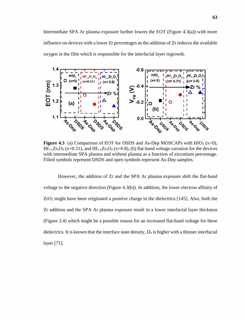
63
Intermediate SPA Ar plasma exposure further lowers the EOT (Figure 4.3(a)) with more
influence on devices with a lower Zr percentages as the addition of Zr reduces the available
oxygen in the film which is responsible for the interfacial layer regrowth.
Figure 4.3 (a) Comparison of EOT for DSDS and As-Dep MOSCAPs with HfO2 (x=0),
Hf1-xZrxO2 (x=0.31), and Hf1-xZrxO2 (x=0.8), (b) flat-band voltage variation for the devices
with intermediate SPA plasma and without plasma as a function of zirconium percentage.
Filled symbols represent DSDS and open symbols represent As-Dep samples.
However, the addition of Zr and the SPA Ar plasma exposure shift the flat-band
voltage to the negative direction (Figure 4.3(b)). In addition, the lower electron affinity of
ZrO2 might have been originated a positive charge in the dielectrics [145]. Also, both the
Zr addition and the SPA Ar plasma exposure result in a lower interfacial layer thickness
(Figure 3.4) which might be a possible reason for an increased flat-band voltage for these
dielectrics. It is known that the interface state density, Dit is higher with a thinner interfacial
layer [71].
(a)
(b)
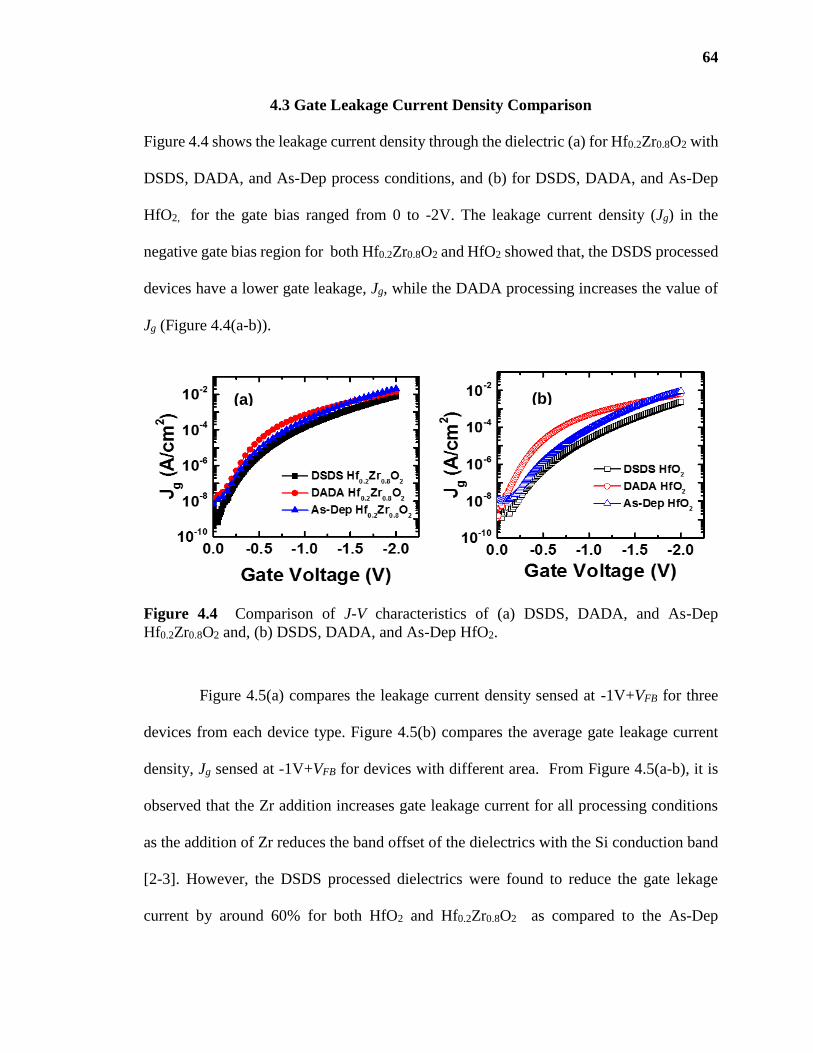
64
4.3 Gate Leakage Current Density Comparison
Figure 4.4 shows the leakage current density through the dielectric (a) for Hf0.2Zr0.8O2 with
DSDS, DADA, and As-Dep process conditions, and (b) for DSDS, DADA, and As-Dep
HfO2, for the gate bias ranged from 0 to -2V. The leakage current density (Jg) in the
negative gate bias region for both Hf0.2Zr0.8O2 and HfO2 showed that, the DSDS processed
devices have a lower gate leakage, Jg, while the DADA processing increases the value of
Jg (Figure 4.4(a-b)).
Figure 4.4 Comparison of J-V characteristics of (a) DSDS, DADA, and As-Dep
Hf0.2Zr0.8O2 and, (b) DSDS, DADA, and As-Dep HfO2.
Figure 4.5(a) compares the leakage current density sensed at -1V+VFB for three
devices from each device type. Figure 4.5(b) compares the average gate leakage current
density, Jg sensed at -1V+VFB for devices with different area. From Figure 4.5(a-b), it is
observed that the Zr addition increases gate leakage current for all processing conditions
as the addition of Zr reduces the band offset of the dielectrics with the Si conduction band
[2-3]. However, the DSDS processed dielectrics were found to reduce the gate lekage
current by around 60% for both HfO2 and Hf0.2Zr0.8O2 as compared to the As-Dep
(a) (b)
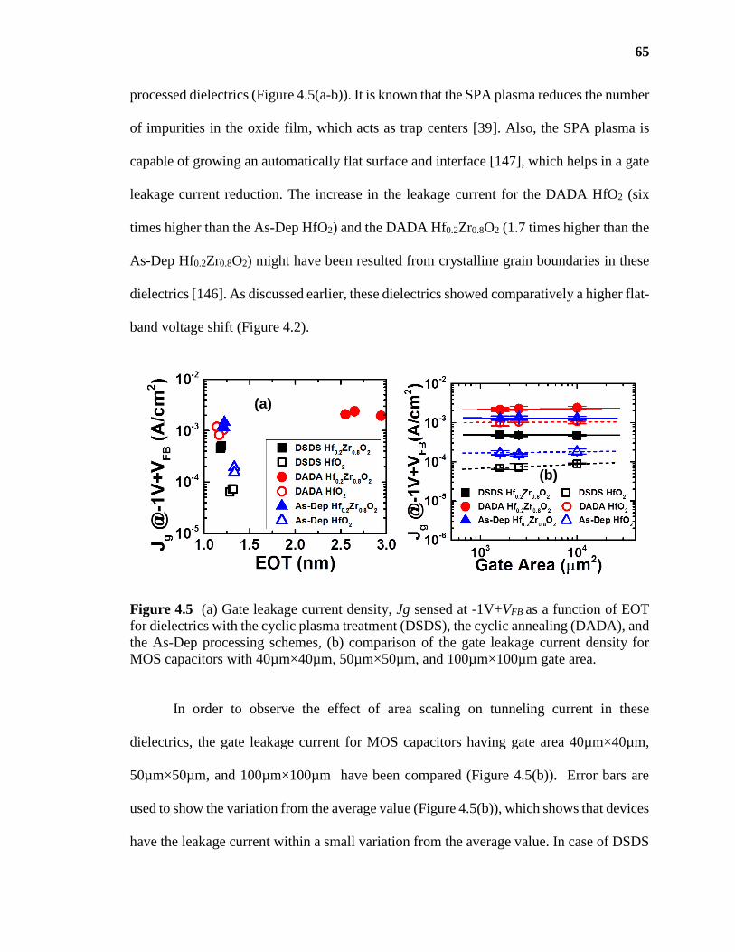
65
processed dielectrics (Figure 4.5(a-b)). It is known that the SPA plasma reduces the number
of impurities in the oxide film, which acts as trap centers [39]. Also, the SPA plasma is
capable of growing an automatically flat surface and interface [147], which helps in a gate
leakage current reduction. The increase in the leakage current for the DADA HfO2 (six
times higher than the As-Dep HfO2) and the DADA Hf0.2Zr0.8O2 (1.7 times higher than the
As-Dep Hf0.2Zr0.8O2) might have been resulted from crystalline grain boundaries in these
dielectrics [146]. As discussed earlier, these dielectrics showed comparatively a higher flat-
band voltage shift (Figure 4.2).
Figure 4.5 (a) Gate leakage current density, Jg sensed at -1V+VFB as a function of EOT
for dielectrics with the cyclic plasma treatment (DSDS), the cyclic annealing (DADA), and
the As-Dep processing schemes, (b) comparison of the gate leakage current density for
MOS capacitors with 40µm×40µm, 50µm×50µm, and 100µm×100µm gate area.
In order to observe the effect of area scaling on tunneling current in these
dielectrics, the gate leakage current for MOS capacitors having gate area 40µm×40µm,
50µm×50µm, and 100µm×100µm have been compared (Figure 4.5(b)). Error bars are
used to show the variation from the average value (Figure 4.5(b)), which shows that devices
have the leakage current within a small variation from the average value. In case of DSDS
(a)
(b)

66
HfO2, 100µm×100µm capacitors showed a slight increase in Jg as compared to
40µm×40µm, and 50µm×50µm. All other dielectrics showed identical leakage current
density for capacitors with different area (Figure 4.5(b)) which indicates that these
dielectrics have no variation in the defect density with device area. Therefore, in this work
we did the reliability study for MOS capacitors with 40µm×40µm gate area, which is the
lowest size supported by our measurement system.
4.4 Interface State Density, Dit Extraction by Conductance Method
Figure 4.6 shows capacitance voltage characteristics (Figure 4.6(a)), conductance voltage
characteristics (Figure 4.6(b)) measured at frequency range 1 MHz to 100 Hz, and
conductance map as a function of gate bias and measurement frequency (Figure 4.6(c)).
Figure 4.6 (a) Frequency dependent C-V characteristics, (b) G-V characteristics measured
at different frequencies, and (c) map of the normalized parallel conductance Gp/A, as a
function of gate bias and frequency. Measurement frequency was varied from 1 MHz to
100 Hz.
From Figure 4.6(a-b), a significant frequency dispersion is observed both in the
capacitance as well as in the ac conductance. According to recent studies, the frequency
dispersions seen near the accumulation region (Vg<-0.5V in Figure 4.6(a-b)) are because
of border traps present in the dielectrics, while the frequency dispersion (“hump”) seen
67
around 0V is attributed to the interface states in the mid gap region [148-152]. The contour
map of Gp/A (Figure 4.6(c)) also showed an efficient Fermi level movement between
-0.3V to 0.1 V gate bias [72-73]. Therefore, this research has estimated the interface state
density, Dit from the peak value of Gp/A as a function of frequency for the gate bias
between -0.3V to 0.1 V. In this bias voltage range, the effect of uncertainties in the series
resistance and the tunneling current on the extracted Dit is minimal, as the tunneling current
is limited to 10-7 A/cm-2 for all dielectrics in this work [152].
4.4.1 Impact of Zr Addition and SPA Ar Plasma Exposure on Dit
Figure 4.7(a-b) shows the interface state density, Dit at different trap energy level in the Si
band gap for As-Dep Hf1-xZrxO2 (Figure 4.7(a)) and for DSDS Hf1-xZrxO2 (Figure 4.7(b))
with x=0, 0.31, and 0.8. Figure 4.7(c) shows the comparison of the mid-gap Dit as a function
of the EOT for Hf1-xZrxO2 with the DSDS and the As-Dep processing conditions. From
Figure 4.7 (a-b), it can be seen that the interface state density values were observed in the
range of 1010 cm-2eV-1 to 1012 cm-2eV-1, which are in accordance with the reported values
for Si/SiO2 and Si/SiON interfaces [153-154]. It is observed that the Zr addition into HfO2
results in a moderate increase in the Dit within the Si band gap for the As-Dep dielectrics,
while almost identical values were observed for the plasma exposed dielectrics (DSDS)
with different percentage of Zr.

68
Figure 4.7 (a-b) Dit as a function of trap level (Et -Ev : energy difference between trap
level, Et and the majority carrier band edge, Ev) in the Si band gap for As-Dep Hf1-xZrxO2
and for DSDS Hf1-xZrxO2 with x=0, 0.31, and 0.8, and (c) comparison of the mid-gap level
Dit as a function of EOT for different dielectrics.
Also, devices with higher Zr percentage showed a lower EOT, which was further
reduced due to the SPA plasma exposure (Figure 4.7(c)). A slight increase in the mid-gap
Dit has been found for DSDS processed dielectrics as compared to As-dep dielectrics for
HfO2 (x=0), and for Hf1-xZrxO2 with x= 0.31. Whereas identical Dit values were observed
for both DSDS and As-Dep Hf1-xZrxO2 with x=0.8. It was previously reported that both Zr
addition and SPA Ar plasma exposure limit the interfacial layer regrowth by controlling
0.3 0.4 0.5 0.610
10
1011
1012
1013
Dit (cm
-2eV
-1)
Et-E
v (eV)
x=0
x=0.31
x=0.8
0.3 0.4 0.5 0.610
10
1011
1012
1013
Dit (
cm
-2e
V-1)
Et-E
v(eV)
x=0
x=0.31
x=0.8
1.1 1.2 1.3 1.410
10
1011
1012
1013
As-Dep (x=0) DSDS (x=0)
As-Dep (x=0.31) DSDS (x=0.31)
As-Dep (x=0.8 DSDS (x=0.8)
Mid
Ga
p D
it(c
m-2e
V-1)
EOT (nm)
(a) (b)
(c)
As-Dep
Hf1-xZrxO2
DSDS Hf
1-xZr
xO
2
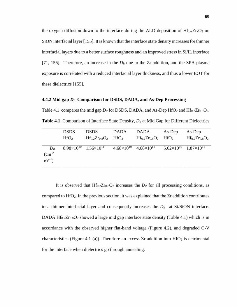
69
the oxygen diffusion down to the interface during the ALD deposition of Hf1-xZrxO2 on
SiON interfacial layer [155]. It is known that the interface state density increases for thinner
interfacial layers due to a better surface roughness and an improved stress in Si/IL interface
[71, 156]. Therefore, an increase in the Dit due to the Zr addition, and the SPA plasma
exposure is correlated with a reduced interfacial layer thickness, and thus a lower EOT for
these dielectrics [155].
4.4.2 Mid gap Dit Comparison for DSDS, DADA, and As-Dep Processing
Table 4.1 compares the mid gap Dit for DSDS, DADA, and As-Dep HfO2 and Hf0.2Zr0.8O2.
Table 4.1 Comparison of Interface State Density, Dit at Mid Gap for Different Dielectrics
DSDS
HfO2
DSDS
Hf0.2Zr0.8O2
DADA
HfO2
DADA
Hf0.2Zr0.8O2
As-Dep
HfO2
As-Dep
Hf0.2Zr0.8O2
Dit
(cm-2
eV-1)
8.98×10¹⁰ 1.56×10¹¹ 4.68×10¹⁰ 4.68×10¹¹ 5.62×10¹⁰ 1.87×10¹¹
It is observed that Hf0.2Zr0.8O2 increases the Dit for all processing conditions, as
compared to HfO2. In the previous section, it was explained that the Zr addition contributes
to a thinner interfacial layer and consequently increases the Dit at Si/SiON interface.
DADA Hf0.2Zr0.8O2 showed a large mid gap interface state density (Table 4.1) which is in
accordance with the observed higher flat-band voltage (Figure 4.2), and degraded C-V
characteristics (Figure 4.1 (a)). Therefore an excess Zr addition into HfO2 is detrimental
for the interface when dielectrics go through annealing.
70
4.5 Chapter Summary
In this chapter, electrical characteristics of ALD Hf1-xZrxO2 deposited by the DSDS (cyclic
SPA Ar plasma treatment) and the DADA (cyclic deposition and annealing) processing
conditions were studied and compared with the standard as deposited (As-Dep) processing.
It was found that the addition of Zr and the SPA plasma exposure helps EOT downscaling.
DADA Hf0.2Zr0.8O2 on the other hand showed a degraded characteristics. The addition of
Zr into HfO2 showed to increase the flat-band voltage slightly. Also, the gate leakage
current density, and the mid-gap Dit value increase with the addition of Zr into HfO2.

71
CHAPTER 5
RELIABILITY STUDY OF ALD Hf1-xZrxO2 WITH CYCLIC DEPOSITION AND
ANNEALING (DADA), AND CYCLIC SPA Ar PLASMA TREATMENT (DSDS)
5.1 Introduction
In this chapter, the reliability study of ALD Hf1-xZrxO2 deposited with the cyclic SPA
plasma treatment (DSDS) and the cyclic annealing (DADA) has been discussed. The
reliability of the devices was observed by subjecting the MOS Capacitors to a constant
voltage stress in the gate injection mode. The applied stress voltage was varied from -2.7V
to -3.4V for different dielectrics according to their EOT and flat-band voltage variation to
have an equal stress field across all dielectrics. Devices were stressed for 1000s and C-V
and I-V characteristics were measured by interrupting the stress in a stress-measurement-
stress cycle. The impact of Zr addition and cyclic treatments (DADA, and DSDS) on the
stress induced flat-band voltage shift (VFB) and the stress induced leakage current (SILC)
were observed and compared. The interface state density (Dit) was compared for unstressed
devices and for devices stressed for 1000s.
Current voltage characteristics at elevated temperature (250C to 1000C) for stressed
(at -2V in the gate injection mode for 500s) and unstressed devices with DSDS and As-
Dep Hf1-xZrxO2 (x=0 and 0.8) were analyzed to understand the evolution of defects in the
dielectrics after stress. The defect activation energy and the SILC activation energy for
these dielectrics were compared from the Arrhenius plots. Also, all dielectrics were
subjected to time dependent dielectric breakdown (TDDB) stress in the gate injection mode
and Weibull plots were compared for further understanding of the break down behavior.
72
In addition, DSDS Hf0.2Zr0.8 has been studied with two different interfacial layers:
(i) SiON formed by UV nitridation of chemically grown oxide on p-Si substrate and (ii)
plasma oxynitride grown after removing chemically grown oxide.
5.2 Impact of Constant Voltage Stress
ALD Hf1-xZrxO2 (x=0, 0.31, and 0.8) prepared by various methods were subjected to a
constant voltage stress in the gate injection mode. Because of a severe degradation, DADA
Hf0.2Zr0.8O2 samples were not considered for any stress measurements. The constant
voltage stress was implemented by applying a negative bias to the gate while keeping the
substrate grounded. The applied stress voltage was varied from -2.7V to -3.4V for different
dielectrics according to their EOT and VFB variation to have an equal stress field across all
dielectrics. When stress is applied, the creation of fixed positive charge centers in the
dielectrics and stress induced interface state generation contributed to the flatband voltage
shift [69, 51-52, 121]. In addition, stress induced traps in the dielectrics increase the gate
leakage current after stress.
5.2.1 Stress Induced Flat-band Voltage Shift (VFB)
5.2.1.1 Comparison for DSDS, DADA, and As-Dep HfO2 and Hf0.2Zr0.8O2. Figure
5.1 shows the flat-band voltage shift as a function of stress time for both HfO2 and
Hf0.2Zr0.8O2 with different processing conditions. The observed stress-induced flat-band
voltage shifts suggest a strong positive charge formation [69, 121]. The overall trends in
stress-induced flat-band voltage shift in HfO2 capacitors with DSDS and DADA processes
are almost identical whereas As-Dep samples show the presence of additional trapping sites
(Figure 5.1) when devices were stressed for more than 100s.

73
Figure 5.1 Flat-band voltage shift (VFB) as a function of stress time for HfO2 with As-
Dep, DSDS, and DADA processing and Hf0.2Zr0.8O2 with As-Dep, and DSDS processing
conditions.
From Figure 5.1, the improvement in stress induced flat-band voltage shift due to
Zr addition is clear. In the case of As-Dep Hf0.2Zr0.8O2 the flat-band voltage shift shows an
initial increase after 20s stress which remains almost similar up to 200s stress. As-Dep
HfO2, on the other hand, showed a significant increase in the flat-band voltage shift after
100s stress. When the devices were stressed for 200s, As-Dep Hf0.2Zr0.8O2 showed more
than 200 mV reduced flat-band voltage shift as compared to As-Dep HfO2 (Figure 5.1).
Even though stress-induced positive charge formation was observed, ZrO2 addition seems
to reduce the number of stress-induced trapping sites [17-21, 56] in the dielectric (Figure
5.1). Devices with DSDS Hf0.2Zr0.8O2 also have improved stress induced flat-band voltage
shift as compared to DSDS HfO2 devices. At lower level stress (within 100s stress
duration), a four times reduction in VFB was observed for DSDS Hf0.2Zr0.8O2 as compared
to As-Dep Hf0.2Zr0.8O2 (Figure 5.1). Once the stress induced charging exceeds a certain
level, electron trapping dominates for DSDS and DADA HfO2 in contrast to devices with
74
Hf0.2Zr0.8O2 which is depicted as a positive flat-band voltage shift after 100s stress (Figure
5.1).
In addition to the improvement observed due to the Zr addition, the intermediate
SPA plasma treatment seems to improve the Hf0.2Zr0.8O2 film characteristics further.
Unlike the devices with DSDS Hf0.2Zr0.8O2, no significant improvement is observed for
DSDS HfO2 as compared to As-Dep HfO2 at low level stress. But after 200s stress, DSDS
HfO2 showed around 150 mV reduced flat-band voltage shift as compared to As-Dep HfO2
(Figure 5.1). For the DSDS processed devices, ZrO2 incorporation brings a significant
improvement as observed from the comparison of the flat-band voltage shifts (Figure 5.1).
In addition of lower flat-band shift after initial stress (20s-stress), around 250 mV reduced
flat-band voltage shift was observed for DSDS Hf0.2Zr0.8O2 after 200s stress as compared
to DSDS HfO2. Therefore, it can be inferred that the cyclic SPA plasma exposure to
Hf0.2Zr0.8O2 can improve the stress-induced flat-band voltage shift by neutralizing positive
charges in the gate stack at low-level stress, but with increase in stress duration, excess
positive charge formation is possible.
5.2.1.2 Effect of SPA Plasma on VFB for Devices with Different Zr Percentage. As
the intermediate SPA plasma improves the device characteristics for devices with 80%
Zr/(Hf+Zr) content, we compared the effect of SPA plasma for devices with 0%, 31% and
80% Zr/(Hf+Zr) content. Figure 5.2(a) shows the normalized flat-band voltage shift as a
function of stress time for DSDS and As-Dep HfO2 (x=0), Hf1-xZrxO2 (x=0.31), and Hf1-
xZrxO2 (x=0.8), where CV measurements were taken by interrupting the stress in a stress-
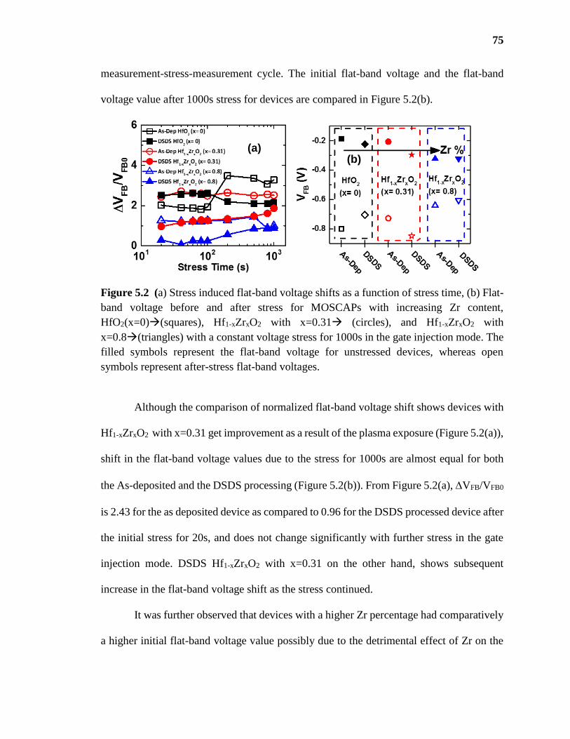
75
measurement-stress-measurement cycle. The initial flat-band voltage and the flat-band
voltage value after 1000s stress for devices are compared in Figure 5.2(b).
Figure 5.2 (a) Stress induced flat-band voltage shifts as a function of stress time, (b) Flat-
band voltage before and after stress for MOSCAPs with increasing Zr content,
HfO2(x=0)(squares), Hf1-xZrxO2 with x=0.31 (circles), and Hf1-xZrxO2 with
x=0.8(triangles) with a constant voltage stress for 1000s in the gate injection mode. The
filled symbols represent the flat-band voltage for unstressed devices, whereas open
symbols represent after-stress flat-band voltages.
Although the comparison of normalized flat-band voltage shift shows devices with
Hf1-xZrxO2 with x=0.31 get improvement as a result of the plasma exposure (Figure 5.2(a)),
shift in the flat-band voltage values due to the stress for 1000s are almost equal for both
the As-deposited and the DSDS processing (Figure 5.2(b)). From Figure 5.2(a), VFB/VFB0
is 2.43 for the as deposited device as compared to 0.96 for the DSDS processed device after
the initial stress for 20s, and does not change significantly with further stress in the gate
injection mode. DSDS Hf1-xZrxO2 with x=0.31 on the other hand, shows subsequent
increase in the flat-band voltage shift as the stress continued.
It was further observed that devices with a higher Zr percentage had comparatively
a higher initial flat-band voltage value possibly due to the detrimental effect of Zr on the
(a) (b)
76
SiON interface [17]. It is known that ZrO2 has comparatively lower electron affinity than
HfO2 [145], which results more positive charge formation in the dielectrics for devices with
x=0.8. Despite a higher initial flat-band voltage value in the negative direction, DSDS HfO2
showed 21% improvement in the stress-induced flat-band voltage shift as compared to As-
Dep HfO2 when devices were compared after 1000 s stress. On the other hand, an
improvement of 12% in the stress-induced flat-band voltage shift was observed for DSDS
Hf1-xZrxO2 with x=0.8 as compared to As-Dep Hf1-xZrxO2 with similar Zr percentage.
Based on this observation, it is inferred that the SPA plasma exposure reduces the impurity
content and provides a significant immunity to the stress-induced trap center formation in
the dielectric thereby improves the reliability of the gate dielectric [39].
5.2.2 Stress Induced Leakage Current (SILC)
5.2.2.1 SILC Comparison for Variation in Processing. Figure 5.3 compares the
normalized stress induced leakage current sensed at -1V for different dielectrics. An
increase in the gate leakage current immediately after the application of stress was observed
for both As-Dep HfO2 and As-Dep Hf0.2Zr0.8O2 (Figure 5.3). The intrinsic traps are the
reason for the possible initial increase in the stress-induced current. A drastic enhancement
in the gate leakage current due to the applied stress has been attributed to the trap assisted
tunneling through pre-existing and newly generated stress induced defects in the high-
layer [53]. Identical behavior was observed for DSDS HfO2 and DSDS Hf0.2Zr0.8O2 at
lower level of stress, while after 200s stress, DSDS Hf0.2Zr0.8O2 showed more than one
order of magnitude reduction in the normalized SILC as compared to DSDS HfO2 (Figure
5.3). On the other hand, As-Dep Hf0.2Zr0.8O2 showed a reduction in the SILC by one orders
of magnitude as compared to As-Dep HfO2 at the low level stress, whereas the difference

77
becomes minimal after 100s stress (Figure 5.3). Also, at the higher-level stress, SILC
increases with stress time in case of As-Dep HfO2, whereas the opposite behavior is
observed in case of As-Dep Hf0.2Zr0.8O2 (Figure 5.3).
Figure 5.3 Comparison of stress induced leakage current (Jg/Jg0) sensed at -1V for
different dielectrics.
From Figure 5.3, a 4 orders of magnitude reduction in the normalized SILC is
observed for both DADA and DSDS HfO2 as compared to As-Dep HfO2 at the low level
stress up to 100s. DSDS Hf0.2Zr0.8O2 also showed a four order of magnitude reduction in
normalized SILC at the low level stress as compared to As-Dep Hf0.2Zr0.8O2. When the
device is under the negative bias condition, electrons first injected to the high- layer,
hopping through the high- layer by trap-assisted-tunneling (TAT) subsequently reach the
conduction band of Si by direct tunneling (DT) through the interfacial layer [155].
Therefore, the SILC behavior of these dielectrics confirms that both DSDS and DADA
processing helps to supress stress induced trap generation at the low level stress, while
additional benefits comes from the Zr addition when the dielectrictric is subjected to the
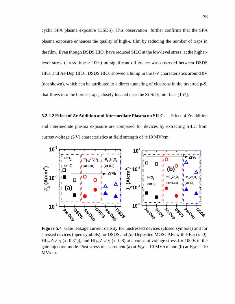
78
cyclic SPA plasma exposure (DSDS). This observation further confirms that the SPA
plasma exposure enhances the quality of high- film by reducing the number of traps in
the film. Even though DSDS HfO2 have reduced SILC at the low-level stress, at the higher-
level stress (stress time > 100s) no significant difference was observed between DSDS
HfO2 and As-Dep HfO2. DSDS HfO2 showed a hump in the I-V characteristics around 0V
(not shown), which can be attributed to a direct tunneling of electrons in the inverted p-Si
that flows into the border traps, closely located near the Si-SiO2 interface [157].
5.2.2.2 Effect of Zr Addition and Intermediate Plasma on SILC. Effect of Zr addition
and intermediate plasma exposure are compared for devices by extracting SILC from
current-voltage (I-V) characteristics at field strength of ±10 MV/cm.
Figure 5.4 Gate leakage current density for unstressed devices (closed symbols) and for
stressed devices (open symbols) for DSDS and As-Deposited MOSCAPs with HfO2 (x=0),
Hf1-xZrxO2 (x=0.31)), and Hf1-xZrxO2 (x=0.8) at a constant voltage stress for 1000s in the
gate injection mode. Post stress measurement (a) at EOX = 10 MV/cm and (b) at EOX = -10
MV/cm.
10-7
10-6
10-5
DSDS
DSDS
DSDS
As-D
ep
As-D
ep
Jg (
A/c
m2)
HfO2
(x= 0)
Hf1-x
ZrxO
2
(x= 0.31)
Hf1-x
ZrxO
2
(x= 0.8)
Zr%
As-D
ep
10-5
10-3
10-1
101
Jg (
A/c
m2)
DSDS
DSDS
DSDS
As-D
ep
As-D
ep
HfO2
(x= 0)
Hf1-x
ZrxO
2
(x= 0.31)
Hf1-x
ZrxO
2
(x= 0.8)
Zr%
As-D
ep
(a)
(b)
79
Figure 5.4 shows the gate leakage current density Jg as a function of Zr content,
obtained from the current voltage characteristics for devices at EOX =10 MV/cm in the
positive bias region (Figure 5.4(a)) and in the negative bias region (Figure 5.4(b)) for
unstressed devices and for devices subjected to a constant field stress for 1000s. Figure 5.4
shows that the gate leakage current density in the negative bias at EOX = -10 MV/cm is
approximately three order of magnitude higher as compared to the leakage current density
in the positive bias condition at EOX = 10 MV/cm for unstressed devices. From Figure
5.4(a), improvement in the leakage current is observed due to both Zr addition and plasma
exposure. The gate leakage current in the positive bias region is mainly influenced by the
quality of the interface. As explained earlier, the SPA plasma has comparatively higher
influence on devices with lower Zr percentage, in terms of suppression of oxygen diffusion
to the interface. In addition, the conduction mechanism of electron through the high-IL
gate stack (See band diagram in Figure 3.8) suggest that electrons tunnel form the
conduction band of Si through the thin interfacial layer first by direct tunneling (DT), and
then tunnel through the high-layer by trap assisted tunneling (TAT) (Figure 3.8(a))
during the positive bias condition. Once the gate field increases, electrons tunnel directly
to the conduction band of the high-layer saturating the current. Improvement in the initial
gate leakage current, due to plasma exposure is, therefore, significantly higher for HfO2 as
compared to Hf1-xZrxO2 with x=0.8. But when devices were stressed for 1000s, DSDS Hf1-
xZrxO2 has comparatively lower shift in leakage current density as compared to DSDS HfO2
at EOX = +10 MV/cm (Figure 5.4(a)).
On the other hand, in the negative bias condition, at EOX = -10 MV/cm sense field,
reduction in the stress induced leakage current due to the intermediate SPA plasma seems
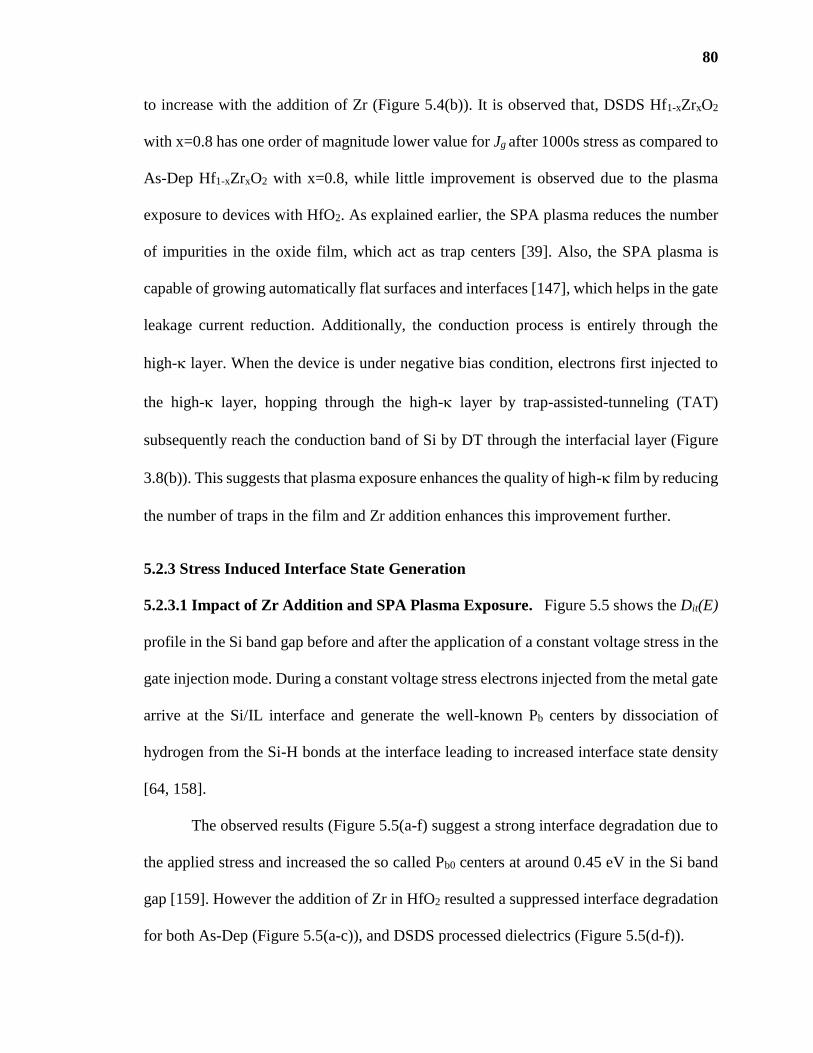
80
to increase with the addition of Zr (Figure 5.4(b)). It is observed that, DSDS Hf1-xZrxO2
with x=0.8 has one order of magnitude lower value for Jg after 1000s stress as compared to
As-Dep Hf1-xZrxO2 with x=0.8, while little improvement is observed due to the plasma
exposure to devices with HfO2. As explained earlier, the SPA plasma reduces the number
of impurities in the oxide film, which act as trap centers [39]. Also, the SPA plasma is
capable of growing automatically flat surfaces and interfaces [147], which helps in the gate
leakage current reduction. Additionally, the conduction process is entirely through the
high- layer. When the device is under negative bias condition, electrons first injected to
the high- layer, hopping through the high- layer by trap-assisted-tunneling (TAT)
subsequently reach the conduction band of Si by DT through the interfacial layer (Figure
3.8(b)). This suggests that plasma exposure enhances the quality of high- film by reducing
the number of traps in the film and Zr addition enhances this improvement further.
5.2.3 Stress Induced Interface State Generation
5.2.3.1 Impact of Zr Addition and SPA Plasma Exposure. Figure 5.5 shows the Dit(E)
profile in the Si band gap before and after the application of a constant voltage stress in the
gate injection mode. During a constant voltage stress electrons injected from the metal gate
arrive at the Si/IL interface and generate the well-known Pb centers by dissociation of
hydrogen from the Si-H bonds at the interface leading to increased interface state density
[64, 158].
The observed results (Figure 5.5(a-f) suggest a strong interface degradation due to
the applied stress and increased the so called Pb0 centers at around 0.45 eV in the Si band
gap [159]. However the addition of Zr in HfO2 resulted a suppressed interface degradation
for both As-Dep (Figure 5.5(a-c)), and DSDS processed dielectrics (Figure 5.5(d-f)).

81
Figure 5.5 Interface state density, Dit in the Si-band gap for unstressed devices (filled
symbols with solid lines) and for stressed devices (open symbols with dashed lines).
Constant voltage stress was applied in the gate injection mode for 1000s. Stress voltage
was ranged between -3V to -3.4V according to the variation of EOT and flat-band voltage
shift for different dielectrics.
0.3 0.4 0.5 0.610
10
1011
1012
1013
Dit (
cm
-2e
V-1)
Et-E
v (eV)
W/o stress
Stressed
0.3 0.4 0.5 0.610
10
1011
1012
1013
Dit (
cm
-2e
V-1)
Et-E
v (eV)
W/o stress
Stressed
0.3 0.4 0.5 0.610
10
1011
1012
1013
Dit (
cm
-2e
V-1)
Et-E
v (eV)
W/o stress
Stressed
0.3 0.4 0.5 0.610
10
1011
1012
1013
Dit (
cm
-2e
V-1)
Et-E
v(eV)
W/o stress
Stressed
0.3 0.4 0.5 0.610
10
1011
1012
1013
Dit (
cm
-2e
V-1)
Et-E
v (eV)
W/o stress
Stressed
0.3 0.4 0.5 0.610
10
1011
1012
1013
Dit (
cm
-2e
V-1)
Et-E
v (eV)
W/o stress
Stressed
As-Dep Hf1-xZrxO2 DSDS Hf1-xZrxO2
(a)
(b)
(c)
(d)
(e)
(f)
(x=0) (x=0)
(x=0.31) (x=0.31)
(x=0.8) (x=0.8)

82
Improved NBTI and TDDB behavior is also reported for increased Zr incorporation
in HfO2 [56, 160]. Zr incorporation in HfO2 leads to a reduced interfacial layer regrowth
during the high- dielectric deposition [107, 155] and thus a better SiON/Si interface
formation as a higher SiOx regrowth can reduce the N concentration in the interface [161-
162]. In addition to Zr addition, cyclic SPA plasma exposure to the dielectrics (DSDS) also
showed a suppressed interface state generation in the Si mid gap level as a result of stress
(Figure 5.5(a-f)).
Figure 5.6 Change in the mid-gap Dit for As-Dep and DSDS Hf1-xZrxO2 with x=0, 0.31,
and 0.8.
Figure 5.6 compares the change in the mid gap Dit after 1000s stress for both As-
Dep and DSDS Hf1-xZrxO2 with x=0, 0.31, and 0.8. A gradual reduction in Dit generation
in the mid gap has been found when the Zr percentage increases which is further reduced
due to the SPA plasma exposure (Figure 5.6). DSDS Hf1-xZrxO2 with 80% Zr/(Hf+Zr)
showed around two order of magnitude reduction in the Dit/Dit0 as compared to As-Dep
HfO2 deposited without an SPA plasma exposure. As described earlier, the SPA plasma
has a low electron energy. The use of Ar plasma reduces the free radical concentration in
the plasma leaving only ground-state low-energy radicals which primarily interact with the
x=0 x=0.31 x=0.8
10-2
10-1
100
101
102
103
D
it/D
it0
Zr/(Hf+Zr) ratio (x)
As-Dep
DSDS
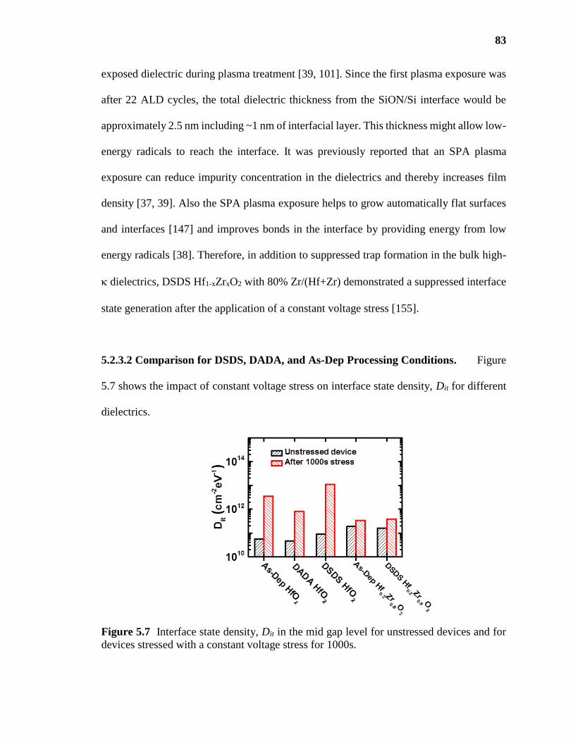
83
exposed dielectric during plasma treatment [39, 101]. Since the first plasma exposure was
after 22 ALD cycles, the total dielectric thickness from the SiON/Si interface would be
approximately 2.5 nm including ~1 nm of interfacial layer. This thickness might allow low-
energy radicals to reach the interface. It was previously reported that an SPA plasma
exposure can reduce impurity concentration in the dielectrics and thereby increases film
density [37, 39]. Also the SPA plasma exposure helps to grow automatically flat surfaces
and interfaces [147] and improves bonds in the interface by providing energy from low
energy radicals [38]. Therefore, in addition to suppressed trap formation in the bulk high-
dielectrics, DSDS Hf1-xZrxO2 with 80% Zr/(Hf+Zr) demonstrated a suppressed interface
state generation after the application of a constant voltage stress [155].
5.2.3.2 Comparison for DSDS, DADA, and As-Dep Processing Conditions. Figure
5.7 shows the impact of constant voltage stress on interface state density, Dit for different
dielectrics.
Figure 5.7 Interface state density, Dit in the mid gap level for unstressed devices and for
devices stressed with a constant voltage stress for 1000s.

84
Devices were stressed for 1000s in the gate injection mode and the mid-gap level
Dit was compared for unstressed devices and for stressed devices. The observed
characteristics showed a severe degradation for DSDS HfO2, and As-Dep HfO2 after 1000s
stress, while a moderate increase in the mid gap Dit is observed for DADA HfO2. As-Dep
Hf0.2Zr0.8O2 and DSDS Hf0.2Zr0.8O2 on the other hand resisted the stress induced interface
degradation after 1000s stress (Figure 5.7). This behavior supports our earlier discussion
of stress induced flat-band voltage shift and SILC characteristics (Figure 5.1 and Figure
5.3).
5.2.4 Time Dependent Dielectric Breakdown
5.2.4.1 Effect of Zr Addition and SPA Plasma on TDDB. To further evaluate the
reliability, the time dependent dielectric break down (TDDB) study was conducted by
subjecting the devices to a constant voltage stress in the gate injection mode. Figure 5.8
shows the change in the current density as a function of time till breakdown for DSDS and
As-Dep Hf1-xZrxO2 with different Zr percentages. All devices demonstrated a slim decrease
in the gate leakage current density due to electron trapping followed by the soft break down
(SBD), the progressive breakdown (PBD) (inset of Figure 5.8), and subsequently, the hard
breakdown (HBD) as stress continued. This behavior is in accordance with previous reports
of the gate dielectric degradation mechanism [75, 86, 131-132]. A critical number of traps
generated in different locations between the anode and the cathode result in a soft
breakdown and as the stress continued, an increased energy dissipation of these localized
areas drives the device into the thermal runway or the hard breakdown [75, 132]. However,
devices with as-deposited Hf1-xZrxO2 with x=0.31and x=0 have the SBD and the PBD
region for very short duration as compared to other devices which is due to their
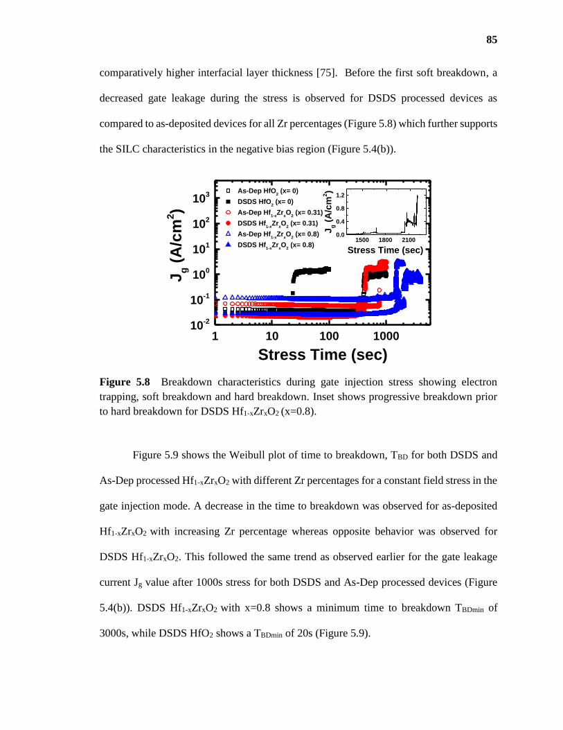
85
comparatively higher interfacial layer thickness [75]. Before the first soft breakdown, a
decreased gate leakage during the stress is observed for DSDS processed devices as
compared to as-deposited devices for all Zr percentages (Figure 5.8) which further supports
the SILC characteristics in the negative bias region (Figure 5.4(b)).
Figure 5.8 Breakdown characteristics during gate injection stress showing electron
trapping, soft breakdown and hard breakdown. Inset shows progressive breakdown prior
to hard breakdown for DSDS Hf1-xZrxO2 (x=0.8).
Figure 5.9 shows the Weibull plot of time to breakdown, TBD for both DSDS and
As-Dep processed Hf1-xZrxO2 with different Zr percentages for a constant field stress in the
gate injection mode. A decrease in the time to breakdown was observed for as-deposited
Hf1-xZrxO2 with increasing Zr percentage whereas opposite behavior was observed for
DSDS Hf1-xZrxO2. This followed the same trend as observed earlier for the gate leakage
current Jg value after 1000s stress for both DSDS and As-Dep processed devices (Figure
5.4(b)). DSDS Hf1-xZrxO2 with x=0.8 shows a minimum time to breakdown TBDmin of
3000s, while DSDS HfO2 shows a TBDmin of 20s (Figure 5.9).
1 10 100 100010
-2
10-1
100
101
102
103
Jg (
A/c
m2)
Stress Time (sec)
As-Dep HfO2 (x= 0)
DSDS HfO2 (x= 0)
As-Dep Hf1-x
ZrxO
2 (x= 0.31)
DSDS Hf1-x
ZrxO
2 (x= 0.31)
As-Dep Hf1-x
ZrxO
2 (x= 0.8)
DSDS Hf1-x
ZrxO
2 (x= 0.8)
1500 1800 21000.0
0.4
0.8
1.2
Jg (
A/c
m2)
Stress Time (sec)
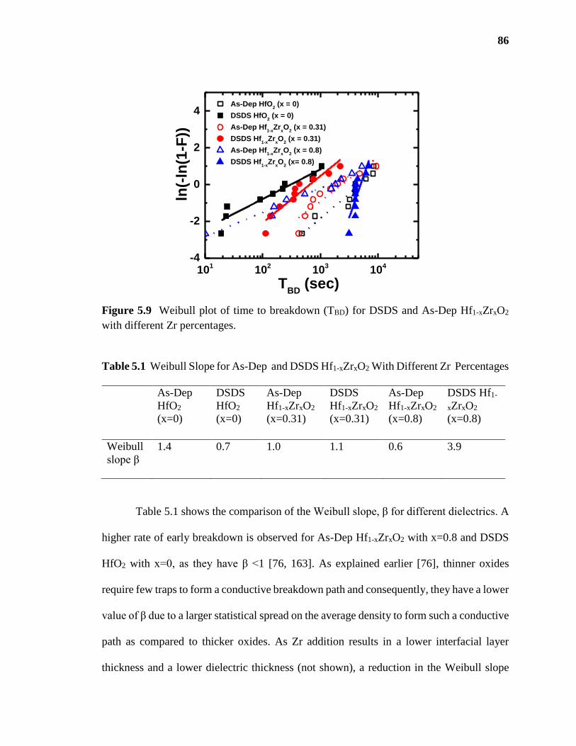
86
Figure 5.9 Weibull plot of time to breakdown (TBD) for DSDS and As-Dep Hf1-xZrxO2
with different Zr percentages.
Table 5.1 Weibull Slope for As-Dep and DSDS Hf1-xZrxO2 With Different Zr Percentages
As-Dep
HfO2
(x=0)
DSDS
HfO2
(x=0)
As-Dep
Hf1-xZrxO2
(x=0.31)
DSDS
Hf1-xZrxO2
(x=0.31)
As-Dep
Hf1-xZrxO2
(x=0.8)
DSDS Hf1-
xZrxO2
(x=0.8)
Weibull
slope β
1.4 0.7 1.0 1.1 0.6 3.9
Table 5.1 shows the comparison of the Weibull slope, β for different dielectrics. A
higher rate of early breakdown is observed for As-Dep Hf1-xZrxO2 with x=0.8 and DSDS
HfO2 with x=0, as they have β <1 [76, 163]. As explained earlier [76], thinner oxides
require few traps to form a conductive breakdown path and consequently, they have a lower
value of β due to a larger statistical spread on the average density to form such a conductive
path as compared to thicker oxides. As Zr addition results in a lower interfacial layer
thickness and a lower dielectric thickness (not shown), a reduction in the Weibull slope
101
102
103
104
-4
-2
0
2
4 As-Dep HfO
2 (x = 0)
DSDS HfO2 (x = 0)
As-Dep Hf1-x
ZrxO
2 (x = 0.31)
DSDS Hf1-x
ZrxO
2 (x = 0.31)
As-Dep Hf1-x
ZrxO
2 (x = 0.8)
DSDS Hf1-x
ZrxO
2 (x= 0.8)
ln(-
ln(1
-F))
TBD
(sec)

87
was observed with an increase in Zr percentage for as-deposited devices (Table 5.1).
Although DSDS processed devices have a thinner dielectric layer and a thinner interfacial
layer, for devices with higher Zr percentages an opposite trend in the Weibull slope, β is
observed with the highest β = 3.9 for DSDS Hf1-xZrxO2 with x=0.8 and the lowest β= 0.7
for DSDS HfO2 with x=0 in this work. This can be explained from the difference in the
electronic structure of HfO2 and ZrO2. Zheng et al. [145] reported that neutral HfO2 and
ZrO2 are highly polar and HfO2 has a higher electron affinity as compared to ZrO2. It is
possible that the SPA plasma introduces excess electrons to HfO2 and ZrO2 during the
processing of DSDS Hf1-xZrxO2. A higher percentage of excess electrons in DSDS HfO2
contributes to form an early percolation path during the stress showing higher degradation
due to stress induced trap generation as compared to devices with higher Zr percentage.
This is because the concentration of excess electron reduces with increase in Zr content.
Therefore, the breakdown characteristics in Figure 5.8 further confirms the SILC
characteristics observed earlier (Figure 5.4(b)) for the negative bias region. In addition,
the reduction of intrinsic traps for DSDS Hf1-xZrxO2 (x=0.8) as compared to As-Dep Hf1-
xZrxO2 with x=0.8 is depicted as a higher Weibull slope for DSDS Hf1-xZrxO2 (x=0.8) due
to an exposure to the intermediate SPA plasma [163].
5.2.4.2 Comparison for Different Processing Conditions. For all of these dielectrics,
statistical analysis using the Weibull distribution has been done and the time to failure,
T63% has been calculated to determine the time for 63% devices to fail due to breakdown.
Table 5.2 lists the failure time, T63% for different dielectrics when they were subjected to a
constant voltage stress in the gate injection mode. From Table 5.2 DSDS Hf0.2Zr08O2

88
showed the highest value T63% = 7834 s, while DSDS HfO2 showed the lowest value T63%
= 1834 s, which is consistent with the earlier discussions. It is clear from the above
discussions that the improvement in DSDS Hf0.2Zr0.8O2 compared to the case of As-Dep is
due to significantly reduced trap concentration in the dielectric.
Table 5.2 Failure Time (T63%) for Different Dielectrics. (Five Devices from Each Device
Type Were Stressed in The Gate Injection Mode until Hard Breakdown)
DSDS
Hf0.2Zr0.8O2
As-Dep
Hf0.2Zr0.8O2
DSDS HfO2 DADA HfO2 As-Dep
HfO2
T63% (s) 7834 3012 1848 6115 4301
5.3 Effect of Quality of Interfacial Layer
While improvement in reliability characteristics is observed with DSDS Hf0.2Zr0.8O2 on
SiON, formed by radial flow nitridation of chemical grown SiO2, the device characteristics
were compared with a different interfacial layer formed by plasma oxynitride grown on Si
after removing the chemically grown oxide.
Figure 5.10 shows the variation in the flat-band voltage and the leakage current
density as a function of the EOT for DSDS Hf0.2Zr0.8O2 deposited on two different
interfacial layers. Figure 5.11 compares the SILC (Figure 5.11(a)) and the VFB (Figure
5.11(b)) as a function of the stress time for these dielectrics. While plasma oxynitride
showed to scale the EOT by around 2Å, it also showed more than 200 mV higher flat-band
voltage shift and an increased leakage current by around one order of magnitude as
compared to SiON (Figure 5.10). The observed results from Figures 5.10 and 5.11
demonstrate that the type of interfacial layer contributed to the gate stack characteristics.
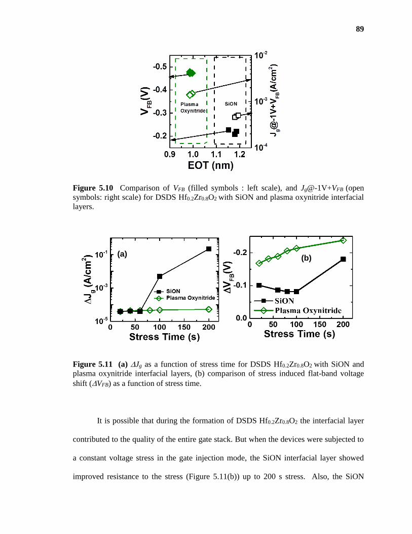
89
Figure 5.10 Comparison of VFB (filled symbols : left scale), and Jg@-1V+VFB (open
symbols: right scale) for DSDS Hf0.2Zr0.8O2 with SiON and plasma oxynitride interfacial
layers.
Figure 5.11 (a) Jg as a function of stress time for DSDS Hf0.2Zr0.8O2 with SiON and
plasma oxynitride interfacial layers, (b) comparison of stress induced flat-band voltage
shift (VFB) as a function of stress time.
It is possible that during the formation of DSDS Hf0.2Zr0.8O2 the interfacial layer
contributed to the quality of the entire gate stack. But when the devices were subjected to
a constant voltage stress in the gate injection mode, the SiON interfacial layer showed
improved resistance to the stress (Figure 5.11(b)) up to 200 s stress. Also, the SiON
(a) (b)

90
showed a low Jg for the low-level stress but it increased with the time as the stress-induced
defect formation continued. The plasma oxynitride, on the other hand, has a very high
defect level with the low-level stress and did not significantly change till 200 s stress
(Figure 5.11). The cumulative failure percentile distribution for DSDS Hf0.2Zr0.8O2 with
the SiON and the plasma oxynitride interfacial layer also demonstrated higher time to
failure, T63% for the SiON (7834s) as compared to the plasma oxynitride (7087s).
5.3.1 Interface State Density Comparison for SiON and Plasma Oxynitride Interface
Figure 5.12(a) compares the Dit(E) distributions in the Si band gap for two different
interfacial layers, while comparison of the mid-gap Dit for unstressed devices and for
stressed devices (1000s stress) is shown in Figure 5.12(b). From Figure 5.12(a), around
one order of magnitude increase in the mid-gap level Dit is observed for the plasma
oxynitride interface as compared to the SION interface.
Figure 5.12 (a) Dit in the Si band gap for SiON and plasma oxynitride interfacial layer,
and (b) change in mid gap Dit for two different type of interfacial layer.
Samples with the SiON exhibit one order of magnitude lower interface state density
as compared to samples with plasma oxynitride interfacial layer. Nitrogen incorporation to
1010
1011
1012
1013
Plasma
oxynitride
Mid
Gap
Dit (
cm
-2eV
-1)
W/o stress
Stressed
SiO
N0.3 0.4 0.5 0.6
1010
1011
1012
1013
Dit (
cm
-2e
V-1)
Et-E
v (eV)
SiON
Plasma oxynitride
(a)
(b)
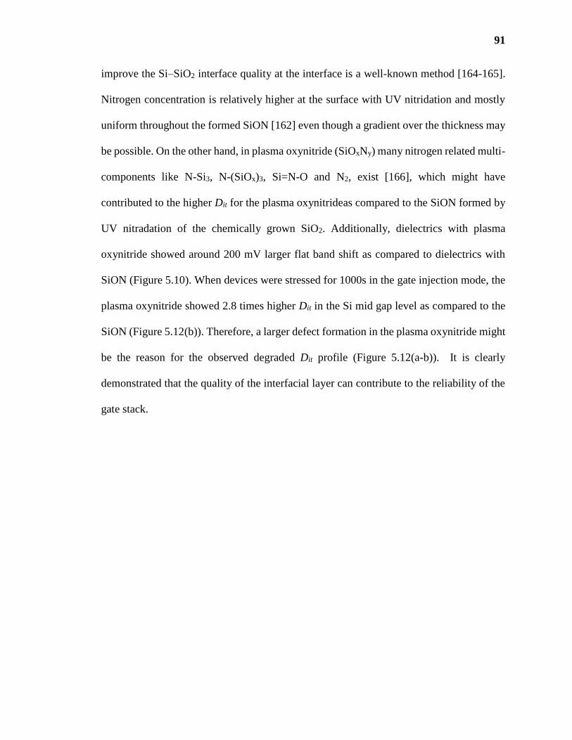
91
improve the Si–SiO2 interface quality at the interface is a well-known method [164-165].
Nitrogen concentration is relatively higher at the surface with UV nitridation and mostly
uniform throughout the formed SiON [162] even though a gradient over the thickness may
be possible. On the other hand, in plasma oxynitride (SiOxNy) many nitrogen related multi-
components like N-Si3, N-(SiOx)3, Si=N-O and N2, exist [166], which might have
contributed to the higher Dit for the plasma oxynitrideas compared to the SiON formed by
UV nitradation of the chemically grown SiO2. Additionally, dielectrics with plasma
oxynitride showed around 200 mV larger flat band shift as compared to dielectrics with
SiON (Figure 5.10). When devices were stressed for 1000s in the gate injection mode, the
plasma oxynitride showed 2.8 times higher Dit in the Si mid gap level as compared to the
SiON (Figure 5.12(b)). Therefore, a larger defect formation in the plasma oxynitride might
be the reason for the observed degraded Dit profile (Figure 5.12(a-b)). It is clearly
demonstrated that the quality of the interfacial layer can contribute to the reliability of the
gate stack.
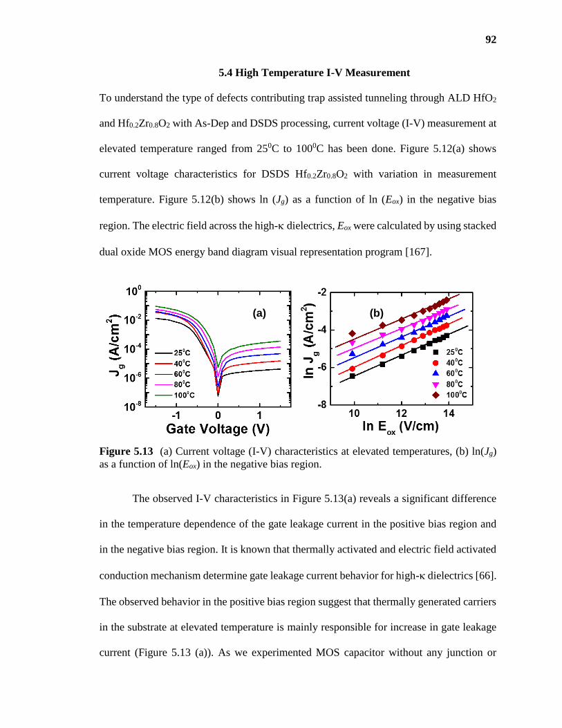
92
5.4 High Temperature I-V Measurement
To understand the type of defects contributing trap assisted tunneling through ALD HfO2
and Hf0.2Zr0.8O2 with As-Dep and DSDS processing, current voltage (I-V) measurement at
elevated temperature ranged from 250C to 1000C has been done. Figure 5.12(a) shows
current voltage characteristics for DSDS Hf0.2Zr0.8O2 with variation in measurement
temperature. Figure 5.12(b) shows ln (Jg) as a function of ln (Eox) in the negative bias
region. The electric field across the high-dielectrics, Eox were calculated by using stacked
dual oxide MOS energy band diagram visual representation program [167].
Figure 5.13 (a) Current voltage (I-V) characteristics at elevated temperatures, (b) ln(Jg)
as a function of ln(Eox) in the negative bias region.
The observed I-V characteristics in Figure 5.13(a) reveals a significant difference
in the temperature dependence of the gate leakage current in the positive bias region and
in the negative bias region. It is known that thermally activated and electric field activated
conduction mechanism determine gate leakage current behavior for high- dielectrics [66].
The observed behavior in the positive bias region suggest that thermally generated carriers
in the substrate at elevated temperature is mainly responsible for increase in gate leakage
current (Figure 5.13 (a)). As we experimented MOS capacitor without any junction or
(a) (b)
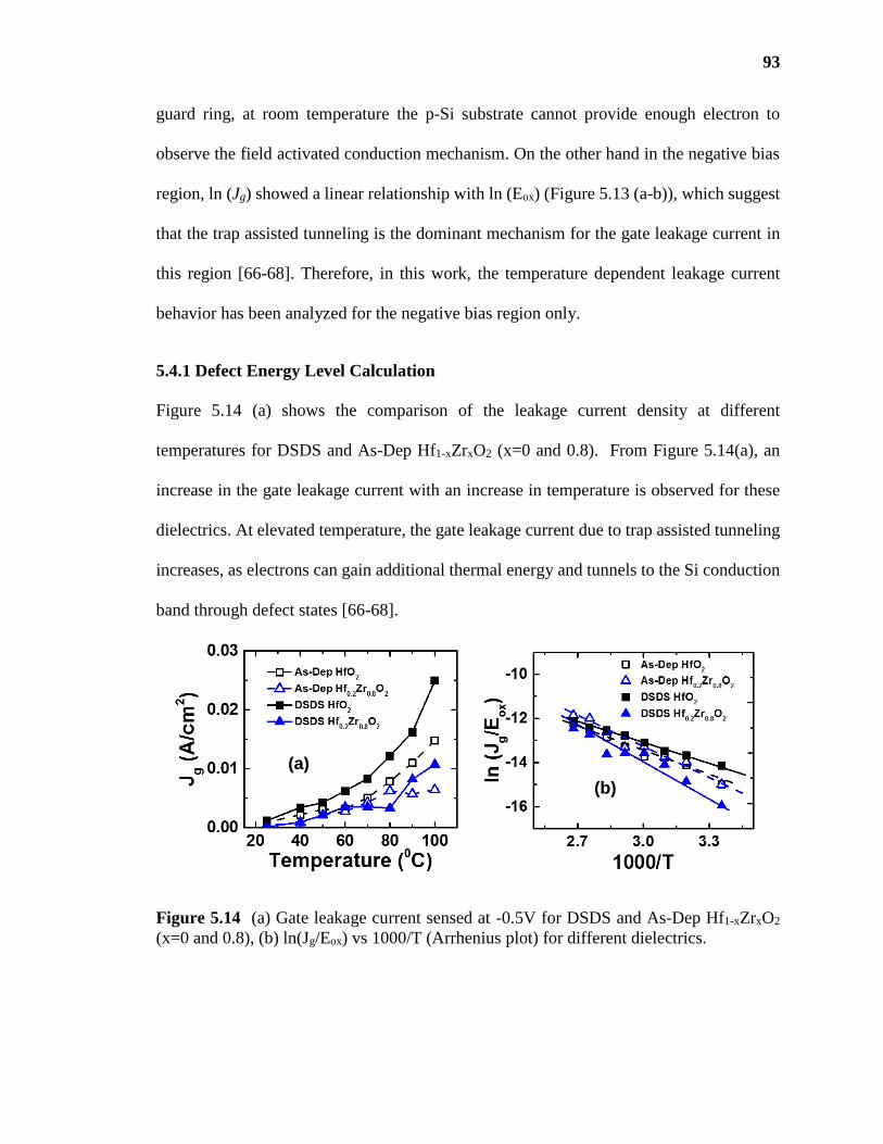
93
guard ring, at room temperature the p-Si substrate cannot provide enough electron to
observe the field activated conduction mechanism. On the other hand in the negative bias
region, ln (Jg) showed a linear relationship with ln (Eox) (Figure 5.13 (a-b)), which suggest
that the trap assisted tunneling is the dominant mechanism for the gate leakage current in
this region [66-68]. Therefore, in this work, the temperature dependent leakage current
behavior has been analyzed for the negative bias region only.
5.4.1 Defect Energy Level Calculation
Figure 5.14 (a) shows the comparison of the leakage current density at different
temperatures for DSDS and As-Dep Hf1-xZrxO2 (x=0 and 0.8). From Figure 5.14(a), an
increase in the gate leakage current with an increase in temperature is observed for these
dielectrics. At elevated temperature, the gate leakage current due to trap assisted tunneling
increases, as electrons can gain additional thermal energy and tunnels to the Si conduction
band through defect states [66-68].
Figure 5.14 (a) Gate leakage current sensed at -0.5V for DSDS and As-Dep Hf1-xZrxO2
(x=0 and 0.8), (b) ln(Jg/Eox) vs 1000/T (Arrhenius plot) for different dielectrics.
(a)
(b)
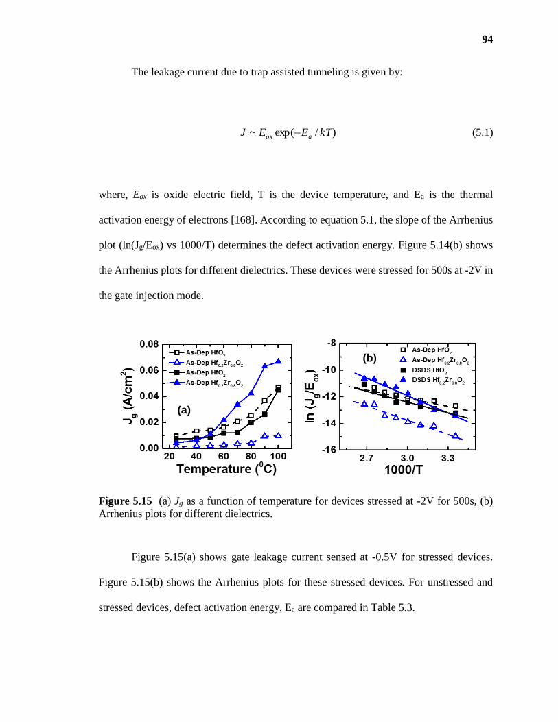
94
The leakage current due to trap assisted tunneling is given by:
)/exp(~ kTEEJ aox (5.1)
where, Eox is oxide electric field, T is the device temperature, and Ea is the thermal
activation energy of electrons [168]. According to equation 5.1, the slope of the Arrhenius
plot (ln(Jg/Eox) vs 1000/T) determines the defect activation energy. Figure 5.14(b) shows
the Arrhenius plots for different dielectrics. These devices were stressed for 500s at -2V in
the gate injection mode.
Figure 5.15 (a) Jg as a function of temperature for devices stressed at -2V for 500s, (b)
Arrhenius plots for different dielectrics.
Figure 5.15(a) shows gate leakage current sensed at -0.5V for stressed devices.
Figure 5.15(b) shows the Arrhenius plots for these stressed devices. For unstressed and
stressed devices, defect activation energy, Ea are compared in Table 5.3.
(a)
(b)

95
Table 5.3 Defect Activation Energy (Ea) for DSDS and As-Dep Hf1-xZrxO2 (x=0 and 0.8)
From Table 5.3, the defects participating trap assisted tunneling are within 0.5 eV
range from the Si conduction band for HfO2 and Hf0.2Zr0.8O2 with the DSDS and the As-
Dep processing. Considering the conduction band offset for HfO2 ~1.5 eV, and for
Hf0.2Zr0.8O2 ~1.4 eV [169], these traps have the defect energy level in the range 1.8 eV to
1.9 eV from the high-conduction band edge.
The observed trap energy levels in Table 5.3 suggest that charged oxygen vacancies
(V+/V2+) are the possible defects in these dielectrics [170-172]. When Zr is added to HfO2
the increase in defect energy level suggest a change in the defect type (Table 5.3). It is
known that Hf-based high-dielectrics are oxygen deficient and therefore, oxygen
diffusion during the ALD deposition contributes to oxygen vacancies (V0/V+) and
interstitials (O0/O-) [173]. During the growth of high- dielectrics, charged and neutral
oxygen interstitials and vacancies can react and modify the defect levels [174]. As earlier
stated, Zr addition limits the oxygen diffusion during ALD deposition [107]. Consequently,
the defect type changes and an increased trap energy level was found for both As-Dep and
DSDS Hf0.2Zr0.8O2 (Table 5.3). Furthermore, the SPA plasma exposure reduces the trap
concentration in the dielectrics and showed a further increase in the defect energy level
[68, 180]. When devices were stressed in the gate injection mode, the generation of stress
As-Dep
HfO2
DSDS HfO2 As-Dep
Hf0.2Zr0.8O2
DSDS
Hf0.2Zr0.8O2
Ea(Unstressed
devices) (eV)
0.32 0.27 0.40 0.48
Ea (Stressed
devices) (eV)
0.18 0.23 0.29 0.38

96
induced defects reduces the defect activation energy [175]. However, DSDS processed
devices showed to suppress the stress induced trap generation in the high- dielectrics
(Table 5.3). The increase in the defect activation energy by Zr addition and the SPA Ar
plasma exposure can explain the higher TBD and the Weibull slope for DSDS Hf0.2Zr0.8O2
(Figure 5.8 and Table 5.1) as observed earlier.
5.4.2 SILC Activation Energy
To further evaluate the temperature dependence of the SILC, these dielectrics have been
subjected to a constant voltage stress at -2V for 500s and the SILC at elevated temperatures
has been evaluated. According to E. Cartier et al. [53] the SILC due to trap assisted
tunneling (TAT) can be described by the following equations:
IgTAT,creation = B(T,Vs) * Ig
DT * t (5.2)
B(T,Vs) = B * Vsb * exp(-Ec/kT) (5.3)
In equation 5.2, IgDT is the direct tunneling current, where Ig
TAT,creation is the current due to
newly generated traps. B(T,Vs) is temperature dependent fitting parameter.

97
Figure 5.16 Arrhenius plot for SILC activation energy for HfO2 and Hf0.2Zr0.8O2 with
DSDS and As-Dep processing conditions. Devices were stressed at -2V in the gate
injection mode for 500s.
Table 5.4 Comparison of SILC Activation Energy (Ec) for DSDS and As-Dep Hf1-xZrxO2
(x=0 and 0.8)
As-Dep HfO2 DSDS HfO2 As-Dep
Hf0.2Zr0.8O2
DSDS
Hf0.2Zr0.8O2
Ec (eV) 0.184 0.217 0.191 0.332
Figure 5.16 shows the Arrhenius plot to estimate SILC activation energy for
different dielectrics. It is found that the activation energy for SILC (Ec) strongly depends
on the processing condition variation (Figure 5.16 and Table 5.4). Both the addition of Zr
and the SPA Ar plasma exposure showed to increase the SILC activation energy Ec for
these dielectrics (Table 5.4). In other words, stress induced trap formation in the dielectrics
reduces. This observation further supports the earlier discussions presented for the same
dielectrics (Figure 5.4).
98
5.5 Chapter Summary
In this chapter, the impact of Zr addition in HfO2 and the impact of intermediate treatments
(cyclic deposition and annealing, DADA and cyclic plasma treatment, DSDS) on the
reliability have been discussed. Zr addition and SPA Ar plasma exposure help EOT
downscaling and enhance the reliability. DSDS Hf0.2Zr0.8O2 showed a suppressed trap
formation due to the applied stress and showed a higher time to breakdown with a steeper
Weibull slope. High temperature I-V measurements also confirmed this behavior. Also the
SiON interfacial layer showed a better performance than the plasma oxynitride when
DSDS Hf0.2Zr0.8O2 was used as the high-dielectric.

99
CHAPTER 6
RELIABILITY STUDY OF DIELECTRICS WITH EXTREMELY
LOW Al INCORPORATION IN HfO2
6.1 Introduction
Over the past decade, HfAlOx with various composition have attracted tremendous
attention for the high-/metal gate stack for CMOS semiconductor devices [22-25, 57-58].
The introduction of Al into HfO2 has been studied by forming HfAlOx alloy structure [22-
31] or HfO2/Al2O3 bilayer structure [23, 32-33]. The incorporation of Al in HfO2 offers
manyfold advantages. These includes an increase in the crystallization temperature, an
improved thermal stability on Si, a reduced gate leakage current etc [22-25]. Recently,
some research showed that HfAlOx films with a higher- value is possible with advanced
ALD deposition process [25, 34]. Although various Hf to Al ratios in different structures
[22-34, 41] were studied, the best combination is yet to be understood. It was found that
the addition of Al beyond some optimal concentration leads to a dielectric quality
degradation [22, 25, 30]. Also, during the post deposition annealing (PDA) process, Al
can diffuse to the high-/metal gate interfaced or to tha Si/SiOx interface [42]. The presence
of an excess Al can also contribute to charge formation by forming a dipole layer [43-45].
Therefore, this research has developed a process technology (Figure 3.5) to incorporate an
extremely low percentage of Al in HfO2. In order to get multifold enhancement of the gate
stack quality, both the Al concentration and the distribution in the dielectrics have been
varied by using an advanced ALD deposition technique.
100
In this work, ALD HfAlOx along with HfO2 in layered structure has been deposited
in a multi-layered gate stack (Figure 3.5). HfAlOx was deposited by using a sequential
precursor pulse method. Details of the device fabrication and physical characteristics of
these dielectrics were discussed in Chapter 3. One set of samples (Lot A) have ALD
HfAlOx as the top layer in a HfO2/HfAlOx bilayer structure. Another set of samples (Lot
B) have ALD HfAlOx as a sandwitched layer in between two ALD HfAlOx layers. The
control sample C has only a HfO2 layer. For Lot A(A1, A2, and A3) and Lot B (B1 and B2)
the number of ALD cycles in HfO2 and HfAlOx layer was varied to obtain the desired Al
percentage in the dielectrics. In this process Al/(Al+Hf) in the range <1% to ~7% has been
obtained in these dielectrics. While all the dielectrics structures used in this work were
subjected to a PDA at 8000C, one set of the multi-layered stacks (dielectrics with 4-5%
Al/Al+Hf) was also annealed at 6800C and 7000C. This chapter discusses about the
electrical characterization and the reliability study of the Al doped HfO2 dielectrics
deposited by using the above advanced process technology. Capacitance voltage (C-V)
characteristics and current voltage (I-V) characteristics for these dielectrics were analyzed
in detail, and compared with the control sample (C) with no Al content. Electrical
characteristics of this dielectrics, which includes the equivalent oxide thickness (EOT), the
flat-band voltage (VFB), the gate leakage current density (Jg), the interface state density
(Dit) were analyzed and explained.
The reliability of high-/metal gate stacks with an extremely low Al incorporation
in HfO2 needs to be carefully studied. In this chapter, reliability study of these dielectrics
done by a constant voltage stress method has been discussed. As dielectrics have variation
in the EOT and the flat-band voltage, the applied stress voltage was varied in the range -
101
2.18V to -2.57V to have an equal stress field across all dielectrics. Stress induced flat-band
voltage shift (VFB), SILC, stress induced interface state generation (Dit), and TDDB
characteristics for dielectrics with <1% to ~7% Al/(Al+Hf) have been discussed. The
power exponent of VFB vs stress time and Jg/Jg0 vs stress time were compared for these
dielectrics. In Chapter 2, the crystallization temperature variation with Al concentration
variation was discussed. It was found that when Al percentage varies from <1% to ~7%,
the crystallization temperature also varies in the range 6800C to 8000C. Therefore,
dielectrics with a higher Al concentration remains amorphous after annealing at 8000C.
Dielectrics with 4-5% Al became partially crystallized after annealing at 8000C, while they
remained amorphous after the PDA at 6800C or 7000C. More focus has been given to
explain the reliability of these dielectrics in terms of the physical properties such as the
crystalline structure, the variation in crystalline grain boundaries, the dielectric thickness
etc.
6.2 Electrical Characteristics of Multi Layered ALD HfAlOx
In order to characterize and compare dielectrics with extremely low Al incorporation in
HfO2, MOS capacitors with p-Si substrate were formed. TiN was used as metal gate and a
chemically grown SiO2 was used as interfacial layer. Electrical characterization of these
devices were done at room temperature.
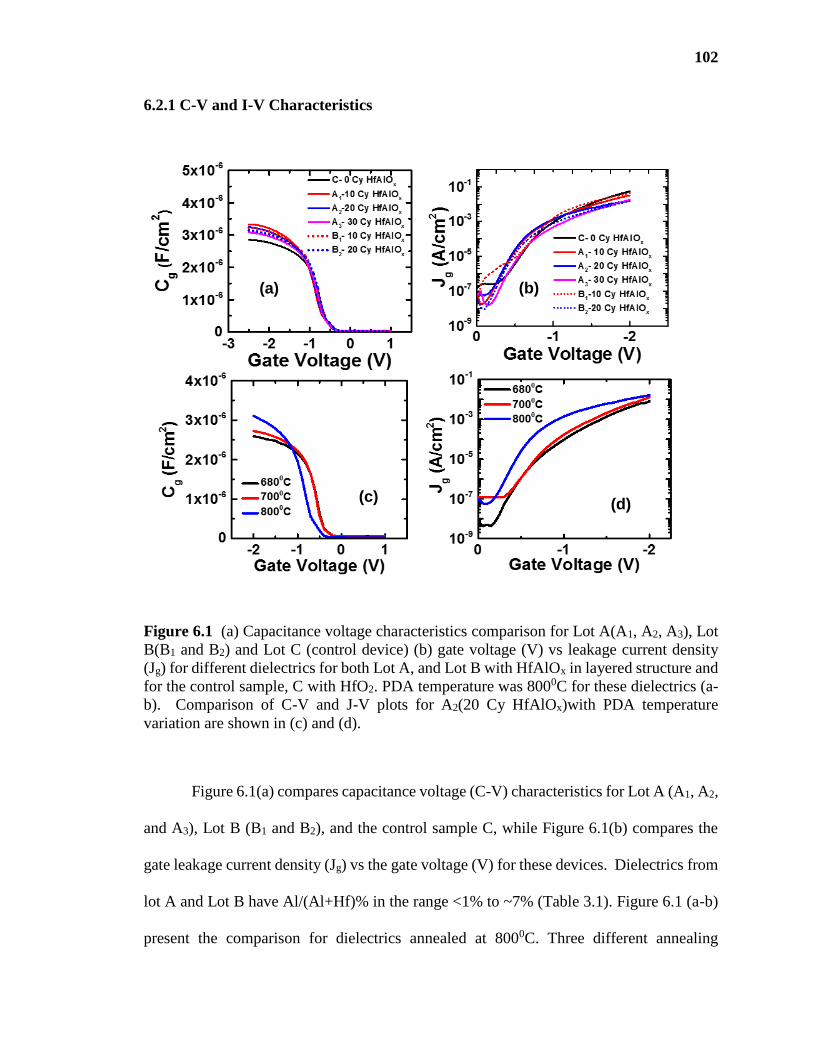
102
6.2.1 C-V and I-V Characteristics
Figure 6.1 (a) Capacitance voltage characteristics comparison for Lot A(A1, A2, A3), Lot
B(B1 and B2) and Lot C (control device) (b) gate voltage (V) vs leakage current density
(Jg) for different dielectrics for both Lot A, and Lot B with HfAlOx in layered structure and
for the control sample, C with HfO2. PDA temperature was 8000C for these dielectrics (a-
b). Comparison of C-V and J-V plots for A2(20 Cy HfAlOx)with PDA temperature
variation are shown in (c) and (d).
Figure 6.1(a) compares capacitance voltage (C-V) characteristics for Lot A (A1, A2,
and A3), Lot B (B1 and B2), and the control sample C, while Figure 6.1(b) compares the
gate leakage current density (Jg) vs the gate voltage (V) for these devices. Dielectrics from
lot A and Lot B have Al/(Al+Hf)% in the range <1% to ~7% (Table 3.1). Figure 6.1 (a-b)
present the comparison for dielectrics annealed at 8000C. Three different annealing
(a) (b)
(c) (d)

103
temperatures (6800C, 7000C, and 8000C) were used for A2 with 20 Cy HfAlOx and they
have 4-5% Al/(Hf+Al) in the dielectrics (Table 3.1). Figure 5.1 (c) compares C-V
characteristics for these dielectrics with a variation in annealing temperature, while Figure
6.1 (d) compares the J-V characteristics. From Figure 6.1(a), an increase in the
accumulation capacitance (Cac) is observed for devices with an HfAlOx layer incorporated
in the gate stack as compared to the control device with HfO2 only. When dielectrics were
annealed at 8000C, A1 with 10 Cy HfAlOx as the top layer showed the highest value for the
Cac. The current voltage characteristics (Figure 6.1 (b)) showed a subsequent reduction in
the gate leakage current density (Jg) with an increased Al incorporation. A3 with 30 Cy
HfAlOx as the top layer showed the lowest value of the Jg (Figure 6.1 (b)). On the other
hand increase in annealing temperature showed an increased value for the Cac (Figure 6.1
(c)) and an increased value for the Jg (Figure 6.1 (d)).
6.2.2 Equivalent Oxide Thickness (EOT), Flat-band Voltage (VFB), and Leakage
Current Density (Jg) Comparison
Figure 6.2(a) plots the flat-band voltage (VFB) as a function of the EOT for all devices
subjected to an annealing at 8000C. Figure 6.2(b) shows the gate leakage current density
sensed at -1V+VFB for these dielectrics. Comparison for the VFB and the leakage current for
dielectrics (A2) annealed at 6800C, 7000C, and 8000C are shown in Figure 6.2(c-d). For
possible variation analysis, three devices from each device type are presented in Figure 6.2
(a-d).
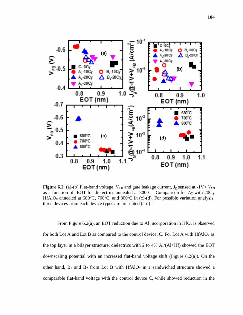
104
Figure 6.2 (a)-(b) Flat-band voltage, VFB and gate leakage current, Jg sensed at -1V+ VFB
as a function of EOT for dielectrics annealed at 8000C. Comparison for A2 with 20Cy
HfAlOx annealed at 6800C, 7000C, and 8000C in (c)-(d). For possible variation analysis,
three devices from each device types are presented (a-d).
From Figure 6.2(a), an EOT reduction due to Al incorporation in HfO2 is observed
for both Lot A and Lot B as compared to the control device, C. For Lot A with HfAlOx as
the top layer in a bilayer structure, dielectrics with 2 to 4% Al/(Al+Hf) showed the EOT
downscaling potential with an increased flat-band voltage shift (Figure 6.2(a)). On the
other hand, B1 and B2 from Lot B with HfAlOx in a sandwiched structure showed a
comparable flat-band voltage with the control device C, while showed reduction in the
(a)
(b)
(c) (d)

105
EOT due to Al incorporation (Figure 6.2(a)). Dielectrics having 10 cycles of HfAlOx from
both Lots showed a significant reduction in the average EOT (18% for A1 and 14% for B1)
as compared to the control device C, with HfO2 only (Figure 6.2(a)). In contrast, A3 with
30 Cy HfAlOx showed only 6% reduction in the average EOT. A3 also showed a higher
EOT variation, while other device types showed the minimal variation for three identical
devices (Figure 6.2(a)). It was found that after 8000C annealing, dielectrics with <2%
Al/(Al+Hf) has a higher crystallization with a mixed structure of monoclinic and tetragonal
phase formation, while an increased Al incorporation inhibits the crystallization process
[34]. On the other hand, the control device C, with HfO2 crystallizes into the monoclinic
phase which is the thermodynamically stable phase for HfO2 [34]. It is known that
tetragonal stabilization of HfO2 results in a higher dielectric constant [25, 34]. Therefore,
dielectrics with 10 Cy HfAlOx from both lots showed a higher EOT downscaling potential
because of a higher crystallization and a tetragonal stabilization (Figure 6.2(a)). The
observed higher flat band voltage for A1 and A2 can be attributed to the grain boundary
related fixed charges, due to a higher crystallization as compared to A3 [146]. In addition,
with an increase in Al concentration, more dipole formation at high-/IL interface can
result in a positive flat-band voltage shift for A2 and A3 as compared to A1 [43, 45].
However, in case of B1 and B2 with intermediate HfAlOx layer, dipoles formed in the
opposite interfaces can cancel each other, and hence, they showed a comparable flat-band
voltage with the control device [44-45]. Less crystallization for A3 with ~7% Al resulted
in a higher EOT with more variation due to an enhanced spatial non homogeneity.
It is clear from Figure 6.2(b) that Al presence in the dielectric reduces the gate
leakage current, which is consistent with the previous reports where the incorporation of
106
Al in HfO2 was found to reduce the gate leakage current due to an increase in the band gap
and the band offset with Si [22-23, 34]. Also, Al addition into HfO2 leads to a smoother
dielectric film surface, which in turn contributes to a smaller leakage current [176].
Therefore, the lowest value of the gate leakage current is observed for the devices with the
highest concentration of aluminum (sample A3) which is in average 70% lower than the
control sample. This can be attributed to an inhibited crystallization process with an
increase in Al content. Since the dielectric remained more amorphous, the leakage current
had reduced. In addition of having a reduced EOT, A1 showed a 41% reduction in the
average gate leakage current density as compared to the control device C (Figure 6.2(b)).
B1 having the lowest Al percentage showed a 32% reduction in the average gate leakage
current, while B2 with 2.56% Al in HfO2 showed a 59% reduction in the average gate
leakage current density.
The observed characteristics in Figure 6.2(c) revealed a significant EOT reduction
(~20%) for dielectrics with 8000C annealing as compared to 6800C, while annealing at
7000C showed slight reduction (~5%) in the EOT. Also dielectrics annealed at 8000C
showed more than 200 mV negative flat-band voltage shift (Figure 6.2(c)), and one order
of magnitude higher leakage current (Figure 6.2(d)) as compared to dielectrics annealed at
6800C and 7000C. As discussed earlier, dielectrics with 20 Cy HfAlOx had a partial
crystallization after annealing at 8000C, while they remained amorphous after annealing at
6800C and 7000C. Therefore, the observed EOT reduction, increased flat-band voltage and
higher leakage current for the dielectric annealed at 8000C can be attributed to its partial
crystallization [34, 146] which is in accordance with our earlier discussions.
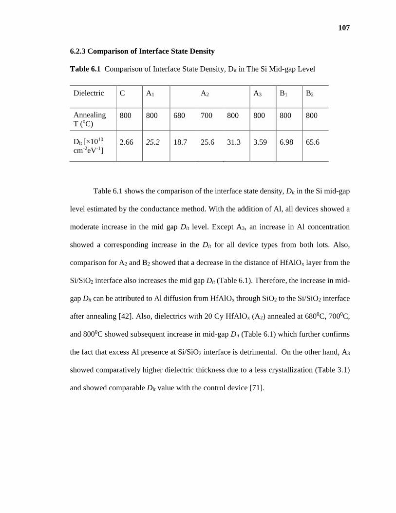
107
6.2.3 Comparison of Interface State Density
Table 6.1 Comparison of Interface State Density, Dit in The Si Mid-gap Level
Table 6.1 shows the comparison of the interface state density, Dit in the Si mid-gap
level estimated by the conductance method. With the addition of Al, all devices showed a
moderate increase in the mid gap Dit level. Except A3, an increase in Al concentration
showed a corresponding increase in the Dit for all device types from both lots. Also,
comparison for A2 and B2 showed that a decrease in the distance of HfAlOx layer from the
Si/SiO2 interface also increases the mid gap Dit (Table 6.1). Therefore, the increase in mid-
gap Dit can be attributed to Al diffusion from HfAlOx through SiO2 to the Si/SiO2 interface
after annealing [42]. Also, dielectrics with 20 Cy HfAlOx (A2) annealed at 6800C, 7000C,
and 8000C showed subsequent increase in mid-gap Dit (Table 6.1) which further confirms
the fact that excess Al presence at Si/SiO2 interface is detrimental. On the other hand, A3
showed comparatively higher dielectric thickness due to a less crystallization (Table 3.1)
and showed comparable Dit value with the control device [71].
Dielectric C A1 A2 A3 B1 B2
Annealing
T (0C) 800 800 680 700 800 800 800 800
Dit [×1010
cm-2eV-1] 2.66 25.2 18.7 25.6 31.3 3.59 6.98 65.6

108
6.3 Reliability Study by Constant Voltage Stress
The reliability of dielectrics can be simply studied by subjecting them to a constant voltage
stress. Details of the stress measurement process was discussed in Chapter 3. Devices were
stressed at a constant voltage stress in the gate injection mode for 1000s and C-V and I-V
measurements were taken by interrupting stress in a stress-measurement-stress-
measurement cycle.
6.3.1 Impact of Stress on VFB, SILC and Dit
Figure 6.3 (a) –(b)Stress induced flat-band voltage shift and SILC as a function of stress
time for dielectrics annealed at 8000C. Applied stress voltage in the gate injection mode
was varied in the range -2.18V to -2.57V according to EOT and VFB variation to have equal
stress field across all dielectrics. Evolution of VFB and SILC as a function of time for A2
annealed at 6800C, 7000C, and 8000C in (c)-(d).
(a)
(b)
(c) (d)
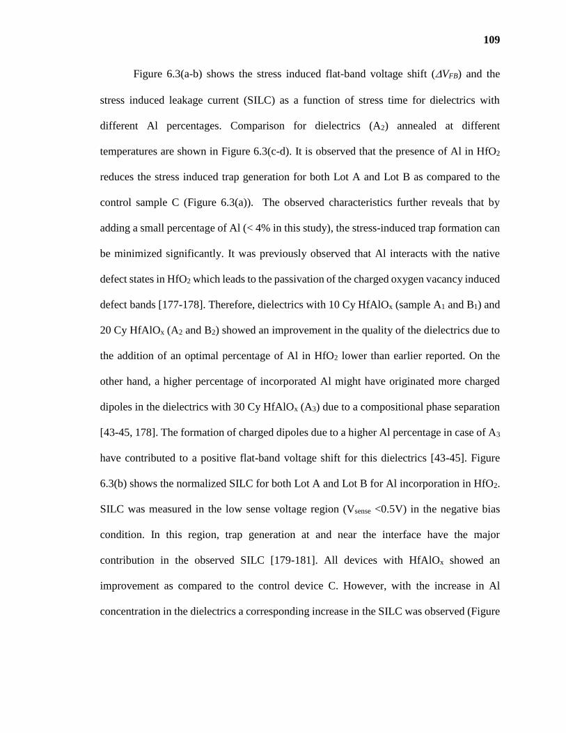
109
Figure 6.3(a-b) shows the stress induced flat-band voltage shift (VFB) and the
stress induced leakage current (SILC) as a function of stress time for dielectrics with
different Al percentages. Comparison for dielectrics (A2) annealed at different
temperatures are shown in Figure 6.3(c-d). It is observed that the presence of Al in HfO2
reduces the stress induced trap generation for both Lot A and Lot B as compared to the
control sample C (Figure 6.3(a)). The observed characteristics further reveals that by
adding a small percentage of Al (< 4% in this study), the stress-induced trap formation can
be minimized significantly. It was previously observed that Al interacts with the native
defect states in HfO2 which leads to the passivation of the charged oxygen vacancy induced
defect bands [177-178]. Therefore, dielectrics with 10 Cy HfAlOx (sample A1 and B1) and
20 Cy HfAlOx (A2 and B2) showed an improvement in the quality of the dielectrics due to
the addition of an optimal percentage of Al in HfO2 lower than earlier reported. On the
other hand, a higher percentage of incorporated Al might have originated more charged
dipoles in the dielectrics with 30 Cy HfAlOx (A3) due to a compositional phase separation
[43-45, 178]. The formation of charged dipoles due to a higher Al percentage in case of A3
have contributed to a positive flat-band voltage shift for this dielectrics [43-45]. Figure
6.3(b) shows the normalized SILC for both Lot A and Lot B for Al incorporation in HfO2.
SILC was measured in the low sense voltage region (Vsense <0.5V) in the negative bias
condition. In this region, trap generation at and near the interface have the major
contribution in the observed SILC [179-181]. All devices with HfAlOx showed an
improvement as compared to the control device C. However, with the increase in Al
concentration in the dielectrics a corresponding increase in the SILC was observed (Figure
110
6.3(b)), which can be attributed to the increased dipole layer charge at high-/SiO2
interface [43-45].
Even though annealing at 8000C was found to degrade the SILC characteristics
(Figure 6.3(d)) as compared to 6800C, and 7000C annealing, in contrast the stress induced
flat-band voltage shift showed an improvement for these dielectrics (Figure 6.3(c)). After
1000s stress duration, dielectrics annealed at 8000C showed 100 mV lower flat-band
voltage shift as compared to the dielectrics annealed at 6800C. As explained earlier, both
bulk and interface charge generation due to the stress contributes to the flat-band voltage
shift, while SILC in the low sense voltage demonstrates trap generation at and near IL.
Higher annealing temperature further drives Al atoms towards the IL, which contributes to
degraded SILC for 8000C annealed sample despite less charge formation in the bulk of
dielectrics as demonstrated by the stress induced flat-band voltage shift.
Both VFB shift and SILC evolution followed a power law function with stress time
as observed from Figure 6.3(a-d). Table 6.2 listed the power exponents (n) for VFB, and
Jg/Jg0 with stress duration for dielectrics with different Al content for both Lot A (A1, A2,
A3), Lot B (B1, B2), and the control device, C. Also, stress induced interface state
generation in the mid gap level after 1000s stress are listed in Table 6.2. Observed stress
induced flat-band voltage shift (Figure 6.3(a) and Table 6.2) suggests that, devices with
~2% Al/(Hf+Al)% (sample: A1) have 55% reduction in the rate of stress induced charge
formation as compared to the control sample with no Al content (sample: C), whereas only
11% reduction was observed for devices with ~7% Al/(Hf+Al)% (sample: A3). Similar
improvement is also observed for B1 (52% reduction).
111
Table 6.2 Power Exponent (n) for VFB, and Jg/Jg0, and Dit/Dit0 Comparison for
Different Dielectrics
Dielectric Annealing
T[0C]
Power
Exponent for
VFB
Power
Exponent for
Jg/Jg0
Dit/Dit0
C-HfO2 800 0.084 1.287 3.58
A1-10Cy
HfAlOx
800 0.037 0.417 1.85
A2-20Cy
HfAlOx
680 0.071 0.441 0.33
700 0.054 0.506 0.52
800 0.039 0.67 4.75
A3-30Cy
HfAlOx
800 0.074 0.758 18.56
B1-10Cy
HfAlOx
800 0.04 0.314 6.83
B2-20Cy
HfAlOx
800 0.052 0.432 13.63
It can be inferred that a low percentage of Al incorporation helps to suppress the
positive charge formation due to the applied stress while an excess positive charge
formation is possible when the Al concentration increases beyond a certain percentage.
Evaluation of the power exponent (n) for Jg/Jg0 with stress time also showed an
improvement for dielectrics with <2% Al/(Hf+Al) (Table 6.2). The lowest value of n
(which is 80% lower as compared to the control device C) was observed for B1 with ~0.6%
Al, while the highest n value (which is 41% lower as compared to the control device C)
was observed for A3 with ~7% Al.

112
When devices were stressed in the gate injection mode, devices with a lower (<4%)
Al concentration (A1, A2, and B1) showed a higher resistance to stress induced interface
state generation in the mid gap level (Table 6.2). A3, and B2 on the other hand showed a
degradation due to applied stress. As discussed earlier, an increase in the HfAlOx layer
thickness or reduction of the distance from the IL was found to increase stress induced
interface state generation in the mid gap level (Figure 3.5(a) and Table 6.2). In addition,
when dielectrics were compared for different PDA temperature, dielectrics annealed at
8000C showed significantly higher interface state generation (Dit/Dit0 ~4) because of a
higher Al diffusion down to the IL as compared to dielectrics annealed at 6800C(Dit/Dit0
~0.3), and at 7000C(Dit/Dit0 ~0.5). This clearly suggests that an excess aluminum presence
at the interface increases the Dit that contributes to the SILC (Figure 6.3(b), and Figure
6.3(d)) as observed earlier. Therefore, an optimized Al concentration in HfO2 and at the
interface can improve the gate stack quality.
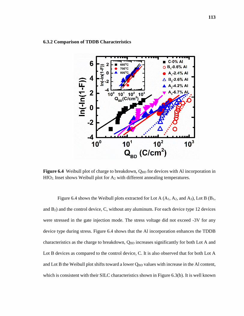
113
6.3.2 Comparison of TDDB Characteristics
Figure 6.4 Weibull plot of charge to breakdown, QBD for devices with Al incorporation in
HfO2. Inset shows Weibull plot for A2 with different annealing temperatures.
Figure 6.4 shows the Weibull plots extracted for Lot A (A1, A2, and A3), Lot B (B1,
and B2) and the control device, C, without any aluminum. For each device type 12 devices
were stressed in the gate injection mode. The stress voltage did not exceed -3V for any
device type during stress. Figure 6.4 shows that the Al incorporation enhances the TDDB
characteristics as the charge to breakdown, QBD increases significantly for both Lot A and
Lot B devices as compared to the control device, C. It is also observed that for both Lot A
and Lot B the Weibull plot shifts toward a lower QBD values with increase in the Al content,
which is consistent with their SILC characteristics shown in Figure 6.3(b). It is well known
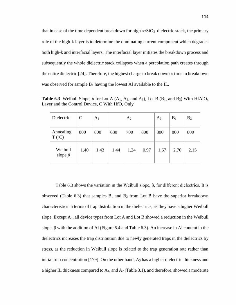
114
that in case of the time dependent breakdown for high-/SiO2 dielectric stack, the primary
role of the high-k layer is to determine the dominating current component which degrades
both high-k and interfacial layers. The interfacial layer initiates the breakdown process and
subsequently the whole dielectric stack collapses when a percolation path creates through
the entire dielectric [24]. Therefore, the highest charge to break down or time to breakdown
was observed for sample B1 having the lowest Al available to the IL.
Table 6.3 Weibull Slope, β for Lot A (A1, A2, and A3), Lot B (B1, and B2) With HfAlOx
Layer and the Control Device, C With HfO2 Only
Dielectric C A1 A2 A3 B1 B2
Annealing
T (0C) 800 800 680 700 800 800 800 800
Weibull
slope β 1.40 1.43 1.44 1.24 0.97 1.67 2.70 2.15
Table 6.3 shows the variation in the Weibull slope, β, for different dielectrics. It is
observed (Table 6.3) that samples B1 and B2 from Lot B have the superior breakdown
characteristics in terms of trap distribution in the dielectrics, as they have a higher Weibull
slope. Except A3, all device types from Lot A and Lot B showed a reduction in the Weibull
slope, β with the addition of Al (Figure 6.4 and Table 6.3). An increase in Al content in the
dielectrics increases the trap distribution due to newly generated traps in the dielectrics by
stress, as the reduction in Weibull slope is related to the trap generation rate rather than
initial trap concentration [179]. On the other hand, A3 has a higher dielectric thickness and
a higher IL thickness compared to A1, and A2 (Table 3.1), and therefore, showed a moderate
115
increase in β. As discussed earlier, thinner oxides require few traps to form a conductive
breakdown path and consequently they have lower value of β due to a larger statistical
spread on the average density to form such a conductive path as compared to thicker oxides
[76]. Similar increase in the Weibull slope was also observed for A2 annealed at 6800C (β=
1.44), and at 7000C (β= 1.24) because of having a higher dielectric thickness as compared
to the dielectrics annealed at 8000C (β =0.97) as shown in Inset of Figure 6.4 and Table
6.3.
From the above observations, increase in Al/(Hf+Al)% contributes to a less
crystallization of the dielectrics even after annealing at 8000C. This characteristic modifies
the EOT for these dielectrics. If the crystallization is higher the dielectric constant increases
and the EOT goes down. Therefore, when dielectrics with same concentration of 4-5%
Al/(Hf+Al) were subjected to 6800C, 7000C, and 8000C annealing, around 20% reduction
in the EOT was observed at a higher temperature annealing (8000C) as compared to a lower
temperature annealing (6800C). Higher crystallization also leads to a higher flat-band
voltage and leakage current by increasing the grain boundary induced charge [146]. In
addition, an increased Al incorporation and a higher crystallization increases the interface
state density due to the Al diffusion to the interface [42]. Furthermore, the stress induced
leakage current and the interface state density behavior for B1 and B2 devices clearly
suggest that when HfAlOx layer is closer to the interface, Dit is higher as the Al
concentration is increased. For low aluminum concentration (<2%) bulk and interface trap
creation showed a significant improvement as evidenced by stress induced flat-band
voltage shift, SILC, Dit, and TDDB characteristics. This can be attributed to the level of
crystallization and availability of aluminum.
116
6.4 Chapter Summary
In this chapter, a comparative study of the electrical characteristics and reliability of ALD
HfAlOx with an extremely low Al content has been presented. A high quality HfO2 based
gate stack by depositing ALD HfAlOx along with HfO2 in a layered structure has been
demonstrated. Electrical characteristics of these dielectrics were found to be influenced by
both Al/(Hf+Al)% and the position of the ALD HfAlOx layer in the stack. An optimized
Al incorporation (<2%) was found to be beneficial for the EOT downscaling and the
reliability enhancement. Also, the annealing temperature has significant influence on their
electrical characteristics and the reliability, since a higher annealing temperature enhances
the crystallization process and facilitates Al diffusion to the interfaces.
117
CHAPTER 7
SUMMARY AND FUTURE WORK
7.1 Summary
In this research, electrical characterization and reliability study have been done for Zr and
Al incorporated Hf-based high-dielectrics with various processing conditions. MOS
capacitors with p-Si substrate and TiN metal gate were fabricated with atomic layer
deposited (ALD) Hf1-xZrxOx and HfAlOx as high- dielectrics. A Cyclic plasma treatment
with SPA Ar plasma (DSDS process) and a cyclic annealing (DADA process) were applied
during the deposition process of ALD Hf1-xZrxO2. DSDS Hf1-xZrxO2 (x=0, 0.31, and 0.8)
and DADA Hf1-xZrxO2 (x=0 and 0.8) were compared with the control sample deposited
with standard as deposited (As-Dep) process. Extremely low percentage of Al (Al/Hf+Al
in the range <1% to ~7%) were incorporated in HfO2 by depositing ALD HfAlOx layer
along with HfO2 layer in a multi layered gate stack. Chemically grown SiO2 interfacial
layer has been used for Al incorporated dielectrics, while SiON formed by radical flow
nitridation of chemically grown SiO2 has been considered for Zr incorporated dielectrics.
Also, DSDS Hf0.2Zr0.8O2 has been studied with another type interfacial layer formed by
depositing plasma oxynitride after removing chemically grown SiO2.
The impact of cyclic plasma treatment with SPA Ar plasma and cyclic annealing
on the equivalent oxide thickness (EOT), the flat-band voltage (VFB), the gate leakage
current density (Jg), and the interface state density (Dit) have been observed for ALD Hf1-
xZrxO2 with different Zr content. Devices were subjected to a constant voltage stress in the
gate injection mode to study the reliability of these dielectrics. Stress induced flat-band

118
voltage shift, VFB, stress induced leakage current, Jg/Jg0, stress induced interface state
generation, Dit were compared for these dielectrics. Also all devices were subjected to
time dependent dielectric breakdown (TDDB) stress in the gate injection mode. It was
observed that DSDS Hf0.2Zr0.8O2 with a SiON interfacial layer exhibits better reliability as
compared to other dielectrics. Zr addition in HfO2 helps the EOT downscaling for DSDS
and As-Dep Hf0.2Zr0.8O2. On the other hand, the film characteristics after ZrO2 addition
were shown to degrade the DADA Hf0.2Zr0.8O2. Suppression of oxide trap formation due
to the cyclic SPA plasma exposure is believed to contribute to a superior Hf0.2Zr0.8O2, EOT
downscaling ability and good reliability performance. Breakdown characteristics suggest
that the devices go through electron trapping, the soft breakdown, the progressive
breakdown and subsequently the hard breakdown. The Weibull characteristic and the
Weibull slope suggest that the variation in electron affinity for HfO2 and ZrO2 contributes
to the improvement in DSDS Hf1-xZrxO2 with x=0.8 by suppressing the oxide trap
formation.
A moderate increase in the Dit was observed due to an increased Zr incorporation
into HfO2, while DSDS processed dielectrics showed an identical Dit (E) profile in the Si
band gap for different Zr percentages. When devices were subjected to a constant voltage
stress in the gate injection mode, the Zr addition and the SPA plasma treatment showed to
result a suppressed stress induced interface state generation by reducing Pbo type Si
dangling bond related defect formation. The improvement due to Zr addition might be
resulted from an improved N incorporattion at the interface by limiting interfacial layer
regrowth, while the SPA plasma provides additional energy to the interface and helps to
improve the surface roughness and bonds at the interface. When DSDS Hf0.2Zr0.8O2 with

119
SiON and plasma oxynitride IL were compared, the latter showed a higher Dit value
possibly due to the presence of some nitrogen related multicomponents in the interfacial
layer.
High temperature I-V measurement results suggest that the Zr addition and the SPA
plasma exposure increase the defect energy level and thereby enhance the reliability for
DSDS Hf0.2Zr0.8O2. Also an increase in the SILC activation energy was observed for DSDS
Hf0.2Zr0.8O2 as compared to other dielectrics. The intermediate SPA plasma exposure
improves the Hf1-xZrxO2 films quality and contributes to minimal variation of interfacial
layer thickness. For EOT scaling we believe thinner Hf1-xZrxO2 will also benefit from this
processing method.
A high quality HfO2 based gate stack by depositing ALD HfAlOx along with HfO2
in a layered structure has been demonstrated in this research. Electrical characteristics of
these dielectrics were found to be influenced by both Al/(Hf+Al)% and the position of the
ALD HfAlOx layer in the stack. Increase in Al/(Hf+Al)% contributes to a less
crystallization of the dielectrics even after annealing at 8000C. This characteristic modifies
the EOT for these dielectrics. If the crystallization is higher, dielectric constant increases
and the EOT goes down. An optimized Al incorporation (<2%) was found to be beneficial
for both EOT downscaling and reliability enhancement. For low aluminum concentration
(<2%) bulk and interface trap creation showed significant improvement as evidenced by
stress induced flat-band voltage shift, SILC, Dit and TDDB. This can be attributed to the
level of crystallization and availability of aluminum. Also annealing temperature has
significant influence on their electrical characteristics and reliability as higher annealing

120
temperature enhances the crystallization process and facilitates Al diffusion to the
interfaces.
7.2 Future Work
7.2.1 ALD Hf1-xZrxO2 and HfAlOx on Si Substrate
Positive bias temperature instability (PBTI) is an important reliability issue for NMOSFET
with high-metal stacks. During the device operation, electron trapping in the dielectrics
due to PBTI stress causes the threshold voltage shift and the SILC generation [55]. More
work is needed to understand the PBTI issues for ALD Hf1-xZrxO2 and HfAlOx deposited
with advanced processing as described in this research.
The interface state density, Dit was estimated by the conductance method at room
temperature. An efficient Fermi level movement was observed around the Si mid gap at
room temperature. Low temperature measurement can be done to obtain the Dit profile in
the full band gap of Si.
7.2.2 Zr and Al Incorporated Hf Based High- Dielectrics on High Mobility
Substrates
Besides Si substrate, the study can be extended to the Ge substrate and the III-V compound
semiconductor channels for more understanding of these noble deposition and processing
conditions. For the high mobility substrate, the interfacial layer growth requires much
attention as the reported interface state density, Dit is significantly higher as compared to
the Si substrate [73, 182-183]. Surface passivation of III-V compound semiconductors by
a thin Al2O3 interfacial layer is a commonly known technique to minimize the Dit [184].
Also a CVD grown Ga rich layer near the GaAs/Al2O3 interface was shown to be promising
121
by Cheng et al. [185]. Recently, Tapily et al.[186] demonstrated an improved electrical
performance for transistor with Ge channel, when a thin Al2O3 passivation layer was used
on SPA grown GeO2 on Ge channel fabricated by Si VLSI compatible toolsets and
infrastructures. These advanced schemes can be used to study the dielectrics presented in
this research on alternative substrates.
122
REFERENCES
[1] http://www.itrs.net/Links/2013ITRS/2013Chapters/2013PIDS.pdf (accessed on
12/14/2014).
[2] D.G. Schlom, S. Guha, and S. Datta, MRS Bull.,vol. 33, p. 1017, 2008.
[3] J. Robertson, J. Appl. Phys., vol. 104, p. 124111, 2008.
[4] http://www.en.wikipedia.org (accessed on 12/14/2014).
[5] L. Wu, K.S. Yew, D.S. Ang, W.J. Liu, T.T. Le, T.L. Duan, C.H. Hou, X.F. Yu,
D.Y. Lee, K.Y. Hsu, J. Xu, H.J. Tao, M. Cao, and H.Y. Yu, IEDM Tech. Dig.,
p. 273, 2010.
[6] L. Wu, H.Y. Yu, K.S. Yew, J. Pan, W.J. Liu, and T.L. Duan, IEEE Trans.
Electron Devices, vol. 58, no. 7, p. 2177, 2011.
[7] R. D. Clark, S. Consiglio, G. Nakamura, Y. Trickett, and G. J. Leusink, ECS
Trans., vol. 41, no. 2, p. 79, 2011.
[8] M.H. Lin, C.H. Hou, J.Y. Wu, and T.B. Wu, J. Electrochem. Soc., vol. 158, no.
3, p. H221, 2011.
[9] C.H. Tu, F.C. Chiu, C.H. Chen, C.H. Hou, Z.J. Lee, H.W. Chen, S.Y. Chen,
H.S. Huang, T.B. Wu, and H.L. Hwang, ECS Trans., vol. 28, no. 2, p. 331, 2010.
[10] A. Delabie, M. Caymax, B. Brijs, D.P. Brunco, T. Conrad, E. Sleeckx, S.
VanElschocht, L. Ragnarsson, S. DeGendt, and M.M. Heyns, J. Electrochem.
Soc.,vol. 153, no. 8, p. F180, 2006.
[11] R. D. Clark, S. Aoyama, S. Consiglio, G. Nakamura, G. Leusink, ECS Trans.,
vol. 35, no. 4, p. 815, 2011.
[12] T. Nabatame , K. Iwamoto, H. Ota, H. Hisamatsu, T. Yasuda, K. Yamamoto, W.
Mizubayashi, Y. Morita , N. Yasuda , M. Ohno, T. Horikawa, and A. Toriumi,
Symp. VLSI Tech., p. 25, 2003.
[13] J. F. Conley, Jr., Y. Ono, and D. J. Tweet, Appl. Phys. Lett., vol. 84, p. 1913,
2004.
[14] D. Ishikawa, S. Kamiyama, E. Kurosawa, T. Aoyama, and Y. Nara, Jpn. J. Appl.
Phys., vol. 48, p. 04C004, 2009.

123
[15] A. Ogawa, K. Iwamoto, H. Ota, M. Takahashi, A. Hirano, T. Nabatame, and
A. Toriumi, Microlectron. Eng., vol. 84, p. 1861, 2007.
[16] S. Consiglio, R. D Clark, E. Bersch, J.D LaRose, I. Wells, K. Tapily, G.J.
Leusink, A.C Diebold, ECS Trans., vol. 41, no. 2, p. 89, 2011.
[17] R.I. Hegde, D.H. Triyoso, P.J. Tobin, S. Kalpat, M.E. Ramon, H.-H. Tseng, J.K.
Schaeffer, E. Luckowski, W.J. Taylor, C.C. Capasso, D.C. Gilmer, M. Moosa,
A. Haggag, M. Raymond, D. Roan, J. Nguyen, L.B. La, E. Hebert, R. Cotton,
X.–D. Wang, S. Zollner, R. Gregory, D. Werho, R.S. Rai, L. Fonseca, M.
Stoker, C. Tracy, B.W. Chan, Y.H. Chiu, B.E. White Jr, IEDM Tech. Dig.,
p. 35, 2005.
[18] R. I. Hegde, D. H. Triyoso, S. B. Samavedam, and B. E. White, J. Appl. Phys.
vol. 101, p. 074113, 2007.
[19] D. H. Triyoso, R. I. Hegde, and J. K. Schaeffer, J. Vac. Sci. Technol. B, vol. 25,
p. 845, 2007.
[20] D. H. Triyoso, R. I. Hegde, J. Jiang, and J. K. Schaeffer, IEEE Electron Dev.
Lett., vol. 29, p. 57, 2008.
[21] C. K. Chiang, J. C. Chang, W. H. Liu, C. C. Liu, J. F. Lin, C. L. Yang , J. Y. Wu,
C. K. Chiang, and S. J. Wang, IEEE IRPS p. GD. 3.1, 2012.
[22] W.J. Zhu, T. Tamagawa, M. Gibson, T. Furukawa, and T.P. Ma, IEEE Electron.
Dev. Lett., vol. 23,no. 11, pp 649-651, 2002.
[23] Y. –K. Chiou, C. –H. Chang, C. –C. Wang, K.–Y. Lee, T.–B. Wu, R. Kwo, and
M. Honga, J. Electrochem. Soc, vol. 154, no. 4, p. G99, 2007.
[24] K. Okada, H. Ota, A. Hirano, A. Ogawa, T. Nabatame, and A. Toriumi, IEEE
IRPS, p. 661, 2008.
[25] P.K. Park, and S.W. Kang, Appl. Phys. Lett., vol. 89,p. 192905, 2006.
[26] M.-Y. Ho, H. Gong, G.D. Wilk, B.W. Busch, M.L. Green, W.H. Lin, A. See,
S.K. Lahiri, M.E. Loomans, P.I. Räisänen, and T. Gustafsson, Appl. Phys. Lett.,
vol. 81,no. 22, p. 4218, 2002.
[27] H.Y. Yu, N. Wu, M.F. Li, C. Zhu, B.J. Cho, D.–L. Kwong, C.H. Tung, J.S. Pan,
J.W. Chai, W.D. Wang, D.Z. Chi, C.H. Ang, J.Z. Zheng, and S. Ramanathan,
Appl. Phys. Lett., vol. 81, no. 19, p. 3618, 2002.
[28] G.D. Wilk, M.L. Green, M.Y. Ho, B.W. Busch, T.W. Scorsch, F.P. Klemens,
B. Brijs, R.B. van Dover, A. Kornblit, T. Gustafsson, E. Garfunkel, S. Hillenius,
D. Monroe, P. Kalavade, and J.M. Hergenrother, VLSI Tech. Dig., p. 88, 2002.

124
[29] V. Mikhelashvili, R. Brener, O. Kreinin, B. Meyler, J. Shneider, and G.
Eisenstein, Appl. Phys. Lett., vol. 85, no. 24, p. 5950, 2004.
[30] T.J. Park, J.H. Kim, J.H. Jang, C.–K. Lee, K.D. Na, S.Y. Lee, H.S. Jung, M.
Kim, S. Han, and C.S. Hwang, Chem. Mater., vol. 22, p. 4175, 2010.
[31] K. Takeda, R. Yamada, T. Imai, T. Fujiwara, T. Hashimoto, and T. Ando, IEEE
Trans. Electron. Dev., vol. 55, no. 6, p. 1359, 2008.
[32] M.-H. Cho, K.B. Chung, H.S. Chang, D.W. Moon, S.A. Park, Y.K. Kim, K.
Jeong, C.N. Whang, D.W. Lee, D.-H. Ko, S.J. Doh, J.H. Lee, and N.I. Lee, Appl.
Phys. Lett., vol. 85, no. 18, p. 4115, 2004.
[33] T. Nishimura, T. Okazawa, Y. Hoshino, Y. Kido, K. Iwamoto, K. Tominaga, T.
Nabatame, T. Yasuda, and A. Toriumi, J. Appl. Phys., vol. 96, no. 11, p. 6113,
2004.
[34] K. Tapily, S. Consiglio, R.D. Clark, R. Vasić, C.S. Wajda, J. J. Sweet, G.J.
Leusink, and A.C. Diebold, ECS Trans., vol. 64, no. 9, p. 123, 2014.
[35] K. Tapily, S. Consiglio, R.D. Clark, R. Vasić, E. Bersch, J. J. Sweet, I.
Wells, G.J. Leusink, and A.C. Diebold, ECS Trans., vol. 45, no. 3, pp. 411- 420,
2012.
[36] D.H. Triyoso, R.I. Hegde, J.K Schaeffer, D. Roan, P.J Tobin, S.B.
Samavedam, B.E. White, R. Gregory, and X.-D. Wang, Appl. Phys. Lett., vol.
88, p. 222901, 2006.
[37] K. Nagata, H. Akamatsu, D. Kosemura, T. Yoshida, M. Takei, M. Hattori,A.
Ogura, T. Koganezawa, M. Machida, J.Y. Son, I. Hirosawa, T. Shiozawa, D.
Katayama, Y. Sato, and Y. Hirota, ECS Trans., vol. 19, no. 9, p. 45, 2009.
[38] K. Kawase, A. Teramoto, H. Umeda, T. Suwa, Y. Uehara, T. Hattori, and T.
Ohmi, J. Appl. Phys., vol. 111, p. 034101, 2012.
[39] T. Tanimura,Y. Watanabe, Y. Sato, Y. Kabe, and Y. Hirota, J. Appl.Phys., vol.
113, p. 064102, 2013.
[40] M. Kobayashi, G. Thareja, M. Ishibashi, Y. Sun, P. Griffin, J. McVittie, P.
Pianetta, K. Saraswat, and Y. Nishi, J. Appl. Phys., vol. 106, p. 104117, 2009.
[41] Q. Li, K.M. Koo, W.M. Lau, P.F. Lee, J.Y. Dai, Z.F. Hou, and X.G. Gong, Appl.
Phys. Lett., vol. 88, no. 18, p. 182903, 2006.
125
[42] W. Wang, K. Akiyama, W. Mizubayashi, T. Nabatame, H. Ota, and A.
Toriumi, J. Appl. Phys., vol. 105, no. 6, p. 064108, 2009.
[43] K. Kita , L.Q. Zhu, T. Nishimura , K. Nagashio and A. Toriumi, ECS Trans., vol.
33, no. 6, p. 463, 2010.
[44] S. Hibino, T. Nishimura, K. Nagashio, K. Kita, and A. Toriumi, ECS Trans.,
vol. 50, no. 4, p. 159, 2012.
[45] K. Iwamoto, A. Ogawa, Y. Kamimuta, Y. Watanabe, W. Mizubayashi, S. Migita,
Y. Morita, M. Takahashi, H. Ito, H. Ota, T. Nabatame, and A. Toriumi,
VLSI Tech. Dig., p. 70, 2007.
[46] J. Robertson, Solid State Electronics, vol. 49, p. 283, 2005.
[47] G. Lucovsky, C.C. Fulton, Y. Zhang, Y. Zou, J. Luning, L. Edge, J.L. Whitten,
R.J. Nemanich, H. Ade, D.G. Schlom, V.V. Afanase'v, SEMATECH
International workshop on Electrical Characterization and Reliability for High-
k Devices, p. 95, 2004.
[48] R. Choi, R. Harris, B.H. Lee, C.D. Young, J.H. Sim, and G. Bersuker,
SEMATECH International workshop on Electrical Characterization and
Reliability for High-k Devices, p. 153, 2004.
[49] M. Houssa, S. DeGendt, G. Groeseneken, and M.M. Heyns, J. Electrochem. Soc.,
vol. 151, no. 12, p. F288, 2004.
[50] A. Kerber, and P. Srinivasan, IEEE Electron. Dev. Lett., vol. 35, no. 4, p. 431,
2014.
[51] M. Cho, B. Kaczer, T. Kauerauf, L.–A. Ragnarsson, and G. Groeseneken, IEEE
Electron. Dev. Lett, vol. 34, no. 5, p. 593, 2013.
[52] Z. Xu, M. Houssa, R. Carter, M. Naili, and S. DeGendt, J. Appl. Phys., vol. 91,
p. 10127, 2002.
[53] E. Cartier and A. Kerber, IEEE IRPS, p. 486, 2009.
[54] F. Crupi, R. Degraeve, A. Kerber, D.H. Kwak, and G. Groeseneken, IEEE IRPS,
p. 181, 2004.
[55] A. Kerber and E. Cartier, IEEE Trans. Dev. and Mat. Rel., vol. 9, no, 2, p. 147,
2009.
126
[56] C. H. Tsai, C.W. Yang, C.H. Hsu, C.M. Lai, K.Y. Lo, C.G. Chen, R.M. Huang,
C.T. Tsai, L.S. Hung, J.W. You, W.H. Hung, T.F. Chen, O. Cheng,
J.Y. Wu, S.F. Tzou, C.W. Liang, and I.C. Chen, Intl. Symp. On VLSI-TSA, p. 1,
2012.
[57] P. Samanta, C.–L. Cheng, and Y.–J. Lee, J. Electrochem. Soc. vol. 156, no. 8, p.
H661, 2009.
[58] J.J. Kim, M. Kim, U. Jung, K.E. Chang, S. Lee, Y. Kim, Y.G. Lee, R. Choi, and
B.H. Lee, IEEE Trans. Electron. Dev, vol. 60, no. 11, p. 3683, 2013.
[59] G.S. May and S.M. Sze, “Ion Implantation,” in Fundamentals of Semiconductor
Fabrication, 2nd ed., Ed. Wiley & Sons, Inc., Danvers, MA, 2004, p. 134.
[60] D.K. Schroder, Microelectronics Reliability, vol. 47, p. 841, 2007.
[61] H.D. Xiong, D. Heh, S. Yang, X. Zhu, M. Gurfinkel, G. Bersuker, D.E. Ioannou,
C.A. Richter, K.P. Cheung and J.S. Suehle, IEEE IRPS, p. 319, 2008.
[62] N. Goel, D. Heh, S. Koveshnikov, I. Ok, S. Oktyabrsky, V. Tokranov, R.
Kambhampati, M. Yakimov, Y. Sun, P. Pianetta, C. K. Gaspe, M. B.Santos, J.
Lee, S. Datta, P. Majhi, and W. Tsai, IEDM Tech. Dig., p. 363, 2008.
[63] J. Huang, N. Goel, H. Zhao, C.Y. Kang, K.S. Min, G. Bersuker, S. Oktyabrsky,
C.K. Gaspe, M.B. Santos, P. Majhi, P.D. Kirsch, H.-H. Tseng, J.C. Lee, and R.
Jammy, IEDM Tech. Dig., p. 1, 2009.
[64] T.J. Ho, D.S. Ang, A.A. Boo, Z.Q. Teo, and K.C. Leong, IEEE Trans. Electron.
Dev., vol. 59, no. 4, p. 1013, 2012.
[65] G. Bersuker, B. Foran, K. van Benthem, S.J. Pennycook, P.M. Lenahan, and J.T.
Ryan, J. Appl.Phy., vol. 100, no. 9, p. 094108, 2006.
[66] N. A. Chowdhury and D. Misra, J. Electrochem. Soc. vol. 154, no. 2, p. G30,
2007.
[67] N. Rahim and D. Misra, IEEE Trans. Dev. and Mat. Rel., vol. 8, no. 4, p. 689,
2008.
[68] S. K. Sahoo and D. Misra, Appl. Phys. Lett., vol. 100, p.232903, 2012.
[69] M. Houssa, “Defect Generation Under Electrical Stress: Experimental
Characterization and Modeling,” in High- Gate Dielectrics, Ed. M. Houssa,
Bristol and Philadelphia: Institute of Physics Publishing, Philadelphia, PA, 2004,
p. 467.
127
[70] S.Zafar, B.H. Lee, and J. Stathis, IEEE Electron. Dev. Lett., vol. 25, no. 3, p.
153, 2004.
[71] P.T. Chen, B.B. Triplett, J.J. Chambers, L. Colombo, P.C. McIntyre, and Y.
Nishi, J. Appl. Phys., vol. 104, p. 014106, 2008.
[72] H.C. Lin, G. Brammertz, K. Martens, G. DeValicourt, L. Negre, W.-E. Wang,
W. Tsai, M. Meuris, and M. Heyns, Appl. Phys. Lett. vol. 94, p. 153508, 2009.
[73] R. E.-Herbert, Y. Hwang, and S. Stemmer, J. Appl. Phys., vol. 108, p. 124101
2010.
[74] G. Bersuker, N. Chowdhury, C. Young, D. Heh, D. Misra, and R. Choi, IEEE
IRPS, p. 49, 2007.
[75] N. Rahim and D. Misra, J. Electrochem. Soc., vol. 155, no. 10, p. G194, 2008.
[76] R. Degraeve, G. Groeseneken, R. Bellens, M. Depas, and H.E. Maes, IEDM
Tech. Dig., p. 863, 1995.
[77] J.E. Lilienfeld, U.S. Patent 1,900,018 (March 7, 1933).
[78] D. Kahng, U.S. Patent 3,102,230 (August 27,1963).
[79] G.E. Moore, Electronics, vol. 38, p. 114, 1965.
[80] M. Houssa and M.M. Heynes, “High-k Dielectrics: Why Do We Need Them?,”
in High- Gate Dielectrics- Ed. by M. Houssa, Bristol and Philadelphia:
Institute of Physics Publishing, Philadelphia, PA, 2004, p. 3.
[81] D.A. Muller, T. Sorsch, S. Moccio, F.H. Baumann, K. Evans-Lutterodt, G.
Timp, Nature, vol. 399, p. 758, 1999.
[82] E. Harari, J. Appl. Phys., vol. 49, p. 2478, 1978.
[83] D.J. DiMaria, E. Cartier, and D. Arnold, J. Appl. Phys., vol. 73, p. 3367, 1993.
[84] D.J. DiMaria, and E. Cartier, J. Appl. Phys., vol. 78, p. 3883, 1995.
[85] R. Degrave, G. Groeseneken, R. Bellens, J.L. Ogier, M. Depas, P.J. Roussel, and
H. Maes, IEEE Trans. Electron Devices, vol. 45, p. 904, 1998.
[86] J.H. Stathis, J. Appl. Phys., vol. 86, p. 5757, 1999.
[87] G.D. Wilk, R.M. Wallace, and J.M. Anthony, J. Appl. Phys., vol. 89, p. 5243,
2001.
128
[88] Z. Jin, H.S. Kwok, M. Wong, IEEE Electron. Dev. Lett., vol. 19, p. 502, 1998.
[89] R. Chau, S. Datta, M. Doczy, B. Doyle, J. Kavalieros, and M. Metz, IEEE
Electron Device Letters, vol. 25, no. 6, p. 408, 2004.
[90] H.-H. Tseng, C.C. Kapasso, J.K. Schaffer, E.A. Hebert, P.T. Jobin, D.C. Gilmer,
D. Triyoso, M.E. Ramon, S.Kalpat, E. Luckowiski, W.J. Taylor, Y. Jeon, O.
Adetutu, R.I. Hegde, R. Noble, M. Jahanbani, C.E. Chemali, B.E. White, IEDM
Tech. Dig., p. 821, 2004.
[91] J. Robertson, J. Non-Crystalline Solids, vol. 303, p.94, 2002.
[92] D. Ceresoli and D. Vanderbilt, Phys. Rev. B, vol. 74, p. 125108, 2006.
[93] M. Gutowski, J.E. Jaffe, C.L. Liu, M. Stoker, R.I. Hegde, R.S. Rai, P.J. Tobin,
Appl. Phys. Lett., vol. 80, p. 1897, 2002.
[94] M. L. Green, J. Appl. Phys., vol. 92, p. 7168, 2002.
[95] T.S. Boscke, P.Y. Hung, P.D. Kirsch, M.A. Quevedo-Lopez, and R. Ramirez-
Bon, Appl. Phys. Lett, vol. 95, p. 052904, 2009.
[96] C.C. Yeo, B.J. Cho, M.S. Joo, S.J. Whoang, D.L. Kwong, L.K. Bera, S. Mathew,
and N. Balasubramanian, Electrochem. Solid State Lett., vol. 6, p. F42, 2003.
[97] M. Takahashi, A. Ogawa, A. Hirano, Y. Kamimuta, Y. Watanabe, K. Iwamoto,
S. Migita, N. Yasuda, H. Ota, T. Nabatame, and A. Toriumi, IEDM Tech. Dig.,
p. 523, 2007.
[98] J.F. Conley, Jr., Y. Ono, R. Solanki, and D.J. Tweet, Mat. Res. Soc. Proc., vol.
765, p. 91, 2004.
[99] J.F. Conley, Jr., D.J. Tweet, Y. Ono, and G. Stecker, Mat. Res. Soc. Proc., vol.
811, p. 5, 2004.
[100] J. Park, B.K. Park, M. Cho, C.S. Hwang, K. Oh, and D.Y. Yang, J. Electrochem.
Soc., vol. 149, p. G89, 2002.
[101] C. Tian, T. Nozawa, K. Ishibasi, H. Kameyama, and T. Morimoto, J. Vac. Sci.
Technol. A, vol. 24, p. 1421, 2006.
[102] M.L. Green, E.P. Gusev, R. Degraeve, and E.L. Garfunkel, J. Appl. Phys., vol.
90, p. 2057, 2001.
[103] T. Okada, M. Shahjahan, K. Sawada, and M. Ishida, Jpn. J. Appl. Phys., Part
1, vol. 44, p. 2320, 2005.
129
[104] M.J. Guittet, J.P. Crocombette, and M. Gautier-Soyer, Phys. Rev. B, vol. 63, p.
125117, 2001.
[105] H. Ota, A. Ogawa, M. Kadoshima, K. Iwamoto, K. Okada, H. Satake, T.
Nabatame, and A. Toriumi, ECS Trans., vol. 3, no. 3, p. 41, 2006.
[106] A. Stesmans and V.V. Afanas’ev, Appl. Phys. Lett., vol. 85, p. 3792, 2004.
[107] S. Ferraria and G. Scarel, J. Appl. Phys., vol. 96, p. 144, 2004.
[108] Method of Fabricating a Gate Dielectric for High-K Metal Gate Devices by C.H.
Chang, C.H. Hou, C.H. Yu, and T.B. Wu, (2010, March 25), United states Patent
Publication No: US 2010/0075507 A1.
[109] H.-S. Jung, S.-A. Lee, S.-H. Rha, S.Y. Lee, H.K. Kim, D.H. Kim, K.H. Oh, J.-
M. Park, W.–H. Kim, M.–W. Song, N.–I. Lee, and C.S. Hwang , IEEE Trans.
Electron. Devices, vol. 58, no. 7, p. 2094, 2011.
[110] J.H. Lee, I.-H. Yu, S.Y. Lee and C.S. Hwang, J. Vac. Sci. Technol. B vol. 32, p.
3 03D109_1, 2014.
[111] D.-Y. Cho et al., Chem. Mater. vol. 24, p. 3534, 2012.
[112] D.-Y. Cho, H. –S. Jung, and C. S. Hwang, Phys. Rev. B, vol. 82, p. 094104,
2010.
[113] M. Stoneham, A. Shluger, A. Foster, M. Szymanski, “Defects and Defect-
Controlled Behavior in High- Materials: A Theoretical Perspective,” High-
Gate Dielectrics, Ed by M. Houssa, Bristol and Philadelphia: Institute of
Physics Publishing, Philadelphia, PA, 2004, p. 294.
[114] J.W. Lim, S.J. Yun, and J.H. Lee, ETRI J. vol. 27, p. 118, 2005.
[115] S.-J. Won, S. Suh, M.S. Huh, and H.J. Kim, IEEE Electron Device Lett. vol. 31,
p. 857, 2010.
[116] D. Hiller, R. Zierold, J. Bachmann, M. Alexe, Y. Yang, J.W. Gerlach, A.
Stesmans, M. Jivanescu, U. Muller, J. Vogt, H. Hilmer, P. Loper, M. Kunle, F.
Munnik, K. Nielsch, and M. Zacharias, J. Appl. Phys., vol. 107, p. 064314,
2010.
[117] J.L. Gavartin, A.L. Shluger, A.S. Foster, and G. Bersuker, J. Appl. Phys., vol.
97, p. 0553704, 2005.
[118] S. Zafar, A. Callegari, E. Gusev, and M.V. Fischetti, J. Appl. Phys., vol. 93, p.
9298, 2003.

130
[119] E.P. Gusev, and C.P. D’Emic, Appl. Phys. Lett., vol. 83, p. 5223, 2003.
[120] Z. Xu, L. Pantisano, A. Kerber, R. Degraeve, E. Cartier, S. DeGendt, M. Heyns,
and G. Groeseneken, IEEE Trans. Electron Dev., vol. 51, p. 402, 2004.
[121] M. Houssa, V.V. Afanas’ev, and A. Stesmans, Appl. Phys. Lett., vol. 79, p. 3134,
2001.
[122] A. Kumar, M.V. Fischetti, T.H. Ning, and E. Gusev, J. Appl. Phys., vol. 94, p.
1728, 2003.
[123] W.Y. Loh, B.J. Cho, M. S.Joo, M.F. Li, D.S.H. Chan, S. Mathew, and D.-L.
Kwong, IEDM Tech. Dig. , p. 927, 2003.
[124] W.-T. Lu, P.-C. Lin, T.-Y. Huang, C.-H.Chien, M.-J. Yang,I.-J. Huang, and P.
Lehnen, Appl. Phys. Lett., vol. 85, p. 3525, 2004.
[125] M. Houssa, V.V. Afanas’ev, A. Stesmans, and M.M. Heyns, Appl. Phys.Lett.,
vol. 77, p. 1885, 2000.
[126] J. Maserijian, and N. Zamani, J. Appl. Phys., vol. 53, p. 559, 1982.
[127] D.J. DiMaria, IEEE Electron Dev. Lett., vol. 16, p. 184, 1995.
[128] R.R. Rofan, and C. Hu, IEEE Electron Device Letters, vol. 12, p. 632, 1991.
[129] D.J. Dumin, IEEE Trans. Electron Dev., vol. 40, p. 986, 1993.
[130] T. Kauerauf, B. Govoreanu, R. Degraeve, G. Groeseneken, and H. Maes, Solid
State Electronics, vol. 49, p. 695, 2005.
[131] S. Lombardo, J.H. Stathis, B.P. Linder, K.L. Pey, F. Palumbo, and C.H. Tung, J.
Appl. Phys., vol. 98, p. 121301, 2005.
[132] F. Mondon, and S. Blonkowski, Microelctron Reliab, vol. 43, p. 1259, 2003.
[133] M. Houssa, T. Nigam, P.W. Mertens, and M.M. Heyns, J. Appl. Phys., vol. 84,
p. 4351, 1998.
[134] J. H. Stathis, and D. J. DiMaria, IEDM Tech. Dig., vol. 126, p. 167, 1998.
[135] J. H. Stathis, IEEE IRPS, p. 132, 2001.
[136] P.J. Roussel, R. Degraeve, S. Sahhaf, and G. Groeseneken, Microelectronic
Engineering, vol. 84, p. 1925, 2007.

131
[137] S. Bruyere, E. Vincent, and G. Ghibaudo, IEEE IRPS, p. 48, 2000.
[138] J. Sune, G. Mura, and E. Miranda, IEEE Electron Device Letters, vol. 21, p. 167,
2000.
[139] J.C. Jackson, T. Robinson, O. Oralkan, and D.J. Dumin, Appl. Phys. Lett., vol.
71, p. 3682, 1997.
[140] J. Sune, and E.Y. Wu, IEDM Tech. Dig., p. 147, 2002.
[141] J. Sune, E.Y. Wu, D. Jimenez, R.P. Vollertsen, and E. Miranda, IEDM Tech.
Dig., p. 117, 2001.
[142] J.R. Hauser and K. Ahmed, AIP Conf. Proc., vol. 449, p. 235, 1998.
[143] E.H. Nicollian and J.R. Brews, MOS (Metal Oxide Semiconductor) Physics
and Technology (Wiley, New York, 1982).
[144] E.H. Nicollian and A. Goetzberger, Bell Syst. Tech. J., vol. 46, p. 1055, 1967.
[145] W. Zheng, K.H. Bowen, Jr., J. Li, I. Daübkowska, and M. Gutowski, J. Phys.
Chem. A, vol. 109, no. 50, p. 11521, 2005.
[146] J. Robertson, J. Vac. Sci. Technol. B vol. 18, p. 1785, 2000.
[147] Y. Kabe, R. Hasunuma, and K. Yamabe, Jpn. J. Appl. Phys., vol. 151, p.
041104, 2012.
[148] S. Stemmer, V. Chobpattan and S. Rajan, Appl. Phys. Lett., vol. 100, p. 233510,
2012.
[149] Y. Yuan, L.Q. Wang, B. Yu, B.H. Shin, J. Ahn, P.C. McIntyre, P.M. Asbeck,
M.J.W. Rodwell, and Y. Taur, IEEE Electron Device Lett. vol. 32, p. 485, 2011.
[150] G.W. Paterson, M.C. Holland, I.G. Thayne, and A.R. Long, J. Appl. Phys., vol.
111, p. 074109, 2012.
[151] G. Brammertz, A. Alian, D.H.C. Lin, M. Meuris, M. Caymax, and W.E. Wang,
IEEE Trans. Electron Dev., vol. 58, p. 3890, 2011.
[152] E.M. Vogel, W.K. Henson, C.A. Richter, and J.S. Suehle, IEEE Trans.
Electron. Dev, vol. 47, no. 3, p. 601, 2000.
[153] S. Kar, ECS Trans, vol. 25, no. 6, p. 399, 2009.
[154] N. Konofaos, and E.K. Evangelou, Semicond. Sci. Technol, vol. 18, p. 56, 2003.

132
[155] M. N. Bhuyian, D. Misra, K. Tapily, R. Clark, S. Consiglio, C. Wajda, G.
Nakamura, and G. Leusink, ECS Journal of Solid State Science and Technology,
vol. 3, no. 5, p. N83, 2014.
[156] J. Songa, K. Kakushimab, P. Ahmeta, K. Tsutsuib, N. Sugiib, T. Hattoria, and
H. Iwaia, Microelectronic Engineering, vol. 84, no. 9, p. 2336, 2007.
[157] E. Kamedaa , T. Matsudab, Y. Emurab, T. Ohzone, Solid State Electron. vol.
43, p. 555, 1999.
[158] M. Houssa, J.L. Autran, A. Stesmans, M.M. Heyns, Appl. Phys. Lett., vol. 81,
no. 4, p. 709, 2002.
[159] J.P. Campbell, P. M. Lenahan, A. T. Krishnan, and S. Krishnan, Appl. Phys.
Lett., vol. 87, no. 20, p. 204106, 2005.
[160] M. Cho, T. Kauerauf, L. –A. Ragnarsson, and G. Groeseneken, IEEE Electron.
Dev. Lett., vol. 34, no. 5, p. 593, 2013.
[161] B.C. Smith, and H.H. Lamb, J. Appl. Phys. vol. 83, p. 7635, 1998.
[162] A. Khandelwal, H. Niimi, G. Lucovsky and H.H. Lamb, J. Vac. Sci. Technol. A,
vol. 20, no. 6, p. 1989, 2002.
[163] Y. Pei, S. Nagamachi, H. Murakami, S. Higashi, S. Miyazaki, T. Kawahara, K.
Torri, Y. Nara, ECS Trans, vol. 1, no. 1, p. 163, 2005.
[164] T. Yamamoto, T. Ogura, Y. Saitio, K. Uwasawa, S. Toru, and T. Mogami, VLSI
Tech. Dig. Symp., vol. 5A, no. 1, p. 45, 1997.
[165] Y. Okada, P. J. Tobin, V. Lakhotia, W. A. Feil, S. A. Ajuria, and R. Hegade,
Appl. Phys. Lett., vol. 63, p. 194, 1993.
[166] H. Jin, S.K. Oh, H.J. Kang, and J.C. Lee, Journal of the Korean Physical Society,
vol. 51, no. 3, p. 1042, 2007.
[167] R.G. Southwick, III, W.B. Knowlton, IEEE Trans. Dev. and Mat. Rel., vol. 6,
no. 2, p. 136, 2006.
[168] S.M. Sze, Physics of Semiconductor Devices, 2nd ed. (Wiley-Interscience, 1981).
[169] J. Robertson and P.W. Peacock, “Electronic Structure and Band Offsets of High
Dielectric-Constant Gate Oxides,” in High- Gate Dielectrics, Ed. By M.
Houssa, Bristol and Philadelphia: Institute of Physics Publishing, Philadelphia,
PA, 2004, p. 391.
133
[170] J.L. Gavartin, D. M. Ramo, A.L. Shluger, and G. Bersuker, in SEMATECH
2nd International Workshop on Advanced Gate Stack Technology, p. 56, 2005.
[171] J. L. Gavartin, L. Fonseca, G. Bersuker, and A.L. Shluger, Microelectron. Eng.,
vol. 80, p. 412, 2005.
[172] K. Torri, K. Shirashi, S. Miyazaki, K. Yamabe, M. Boero, T. Chickyow, K.
Yamada, H. Kitajima, and T. Arikado, IEDM Tech. Dig., p. 129, 2004.
[173] S. Guha, E. Preisler, N. Bojarczuk, and M. Copel, ECS Trans., vol. 1, no. 5, p.
363, 2005.
[174] A.S. Foster, F.L. Gejo, A.L. Shluger, and R.M. Nieminen, Phys. Rev. B, vol. 65,
p. 174117, 2002.
[175] O. Pirrotta, A. Padovani, L. Larcher, L. Zhao, B. Magyari-Köpe, Y. Nishi,
International Conference on Simulation of Semiconductor Processes and
Devices, p. 37, 2014.
[176] W.M. Tang, U. Aboudi, J. Provine, R.T. Howe, and H.–S. Wong, IEEE Trans.
Electron. Dev., vol. 61, no. 7, p. 2398, 2014.
[177] X.F. Wang, Q.Li, R.F. Egerton, P.F. Li, J.Y. Dai, Z.F. Hou, and X.G. Gong, J.
Appl. Phys., vol. 101, no. 1, p. 013514, 2007.
[178] M. Houssa, High- Gate Dielectrics, Edited by M. Houssa, Bristol and
Philadelphia: Institute of Physics Publishing, p. 310, 2004.
[179] D. Ielmini, A. S. Spinelli, A. Rigamonti, and A. L. Lacaita, IEEE Trans.
Electron Dev., vol. 47, no. 6, p. 1266, 2000.
[180] P.E. Nicollian, M. Rodder, D.T. Grider, P. Chen, R.M. Wallace, and S.V.
Hattangady, in Proc. IEEE IRPS., vol. 37, p. 400, 1999.
[181] K. Okada, W. Mizubayashi, N. Yasuda, H. Ota, K. Tominga, K. Iwamoto, T.
Horikawa, K. Yamamoto, H. Hisamatsu, H. Satake, T. Nabatame, and A.
Toriumi, J. Appl. Phys., vol. 97, no. 7, 0745051-7, 2005.
[182] A. Toriumi, C-H. Lee, C. Lu, and T. Nishimura, ECS Trans., vol. 64, no. 8, p.55,
2014.
[183] H.Q. Nguyen, H.D. Trinh, E.Y. Chang, C.T. Lee, S.Y. Wang, H.W. Yu, C.H.
Hsu, and C.L. Nguyen, IEEE Trans. Electron. Dev, vol. 60, no. 1, 2013.
[184] M.L. Huang, Y. C. Chang, C. H. Chang, Y. J. Lee, and P. Chang, J. Kwo, T. B.
Wu and M. Hong, Appl. Phys. Lett., vol. 87, p. 252104, 2005.

134
[185] C.-W. Cheng and E.A. Fitzgerald, Appl. Phys. Lett., vol. 96, p. 202101, 2010.
[186] K. Tapily, T. Ngai, R.D. Clark, D. O’Meara, S. Consiglio, R. Gaylord, C.S.
Wajda, D. Veksler, C. Hobbs, K. Matthews, D.C Gilmer, P. Kirsch, and G.J.
Leusink, ECS Trans., vol. 61, no. 2, p. 89, 2014.


