

DC-DC converter concept allowing line commutated converters and voltage sourceconverters based HVDC systems connectivityElgenedy, Mohamed A. ; Ahmed, Khaled Hani ; Aboushady, Ahmed A. ; Abdelsalam, Ibrahim
Published in:IET Power Electronics
DOI:10.1049/iet-pel.2020.0054
Publication date:2020
Document VersionAuthor accepted manuscript
Link to publication in ResearchOnline
Citation for published version (Harvard):Elgenedy, MA, Ahmed, KH, Aboushady, AA & Abdelsalam, I 2020, 'DC-DC converter concept allowing linecommutated converters and voltage source converters based HVDC systems connectivity', IET PowerElectronics, vol. 13, no. 15, pp. 3294-3304. https://doi.org/10.1049/iet-pel.2020.0054
General rightsCopyright and moral rights for the publications made accessible in the public portal are retained by the authors and/or other copyright ownersand it is a condition of accessing publications that users recognise and abide by the legal requirements associated with these rights.
Take down policyIf you believe that this document breaches copyright please view our takedown policy at https://edshare.gcu.ac.uk/id/eprint/5179 for detailsof how to contact us.
Download date: 03. Apr. 2022

1
A New DC-DC Converter Concept Allowing Line Commutated Converters and Voltage Source Converters Based HVDC Systems Connectivity
M. A. Elgenedy 1,2*, K.H Ahmed1, A.A Aboushady3, and I. Abdelsalam4
1 Current affiliation: Electronic and Electrical Engineering, Strathclyde University, Glasgow G1 1RD, UK
2 Electrical Power Engineering, Alexandria University, Alexandria, Egypt 3 School of Engineering and Built Environment, Glasgow Caledonian University, 70 Cowcaddens Road,
Glasgow, UK 4 Electrical and Control Department, College of Engineering and Technology, Arab Academy for Science,
Technology and Maritime Transport, Cairo, Egypt
*corresponding author: [email protected]
Abstract: The common two challenges in high voltage dc (HVDC) multi-terminal transmission are the dc fault isolation and the dc voltage stepping up/down. Additionally, interconnecting voltage source converter (VSC) and line commutated converters (LCC) based HVDC network topologies has been challenging. This paper, introduces a new dc-dc converter topology concept connecting both LCC and VSC based HVDC networks with bidirectional power flow without operation stoppage. The proposed topology is formed of two front-to-front connected bridges with an ac-link formed of a capacitor and an inductor (which can be replaced by a transformer for voltage step up/down). The LCC-HVDC network bridge is formed of insulated gate commutated thyristors while the VSC-HVDC network bridge is formed of insulated gate bipolar transistors. Therefore, ON/OFF switching of both bridges and bi-directional power flow are possible. Moreover, the reactive power transfer is nullified at rated active power exchange between the proposed converter bridges. The proposed concept detailed analysis and control equations are introduced. Different operation scenarios are simulated. In addition to a scaled-down experimentation to test the applicability of power transfer scenarios without operation stoppage in normal operation.
1. Introduction
High voltage direct current (HVDC) transmission
networks based on voltage source converter (VSC) have been
investigated massively [1]-[3], especially after the proposed
modular multi-level converter (MMC) concept by Marquardt
[4]. Nevertheless, the majority of the existing HVDC
transmission networks are based on line commutated
converter (LCC) using thyristor valves, which are current
source converters (CSC) in nature [5]. Each technology has
its pros and cons, for example, reaching the operation
efficiency level for VSCs as in LCC HVDC networks is still
challenging [6]. In contrast, independent active and reactive
power control as well as power reversal is easier in VSCs, let
alone the absence of the commutation failure [2]. In addition,
the footprint of the LCC based converter station is larger
compared to VSC converter station due to the large reactive
power capacitor banks [6].
Having a robust multi-terminal HVDC network is being
hindered by two main challenges namely: the ability of dc
fault isolation and connection possibility of different dc
voltage level HVDC networks [7]. One of the key solutions
to these challenges is the dual active bridge (DAB) converters
[8]. A DAB dc-dc converter has two conversion stages, where
both involved dc-voltage levels are converted into ac voltages
via dc-ac bridges. The dc-ac bridges are connected front-to-
front (F2F) as in Fig. 1 through an n-turns ratio transformer
connecting two HVDC network terminals to match different
dc voltage levels. The F2F bridges ac waveforms are phase-
shifted to allow power transfer between the HVDC networks.
Several DAB dc-dc topologies have been proposed in
literature for either connecting VSC-HVDC networks; or
LCC-HVDC networks [9]-[16].
Fig. 1. Conceptual DAB converter.
Generally, dc-dc converters can be divided into three main groups as follows [17]-[19]:
• Single-stage dc-dc converter. In this category, the same
current flows between input and output. These
topologies are widely used for switched mode power
supplies (SMPS) and can be isolated or non-isolated.
Moreover, they can step the dc voltages up or down.
Examples for this category are buck, boost, buck-boost
and flyback converters. Nevertheless, the power ratings
for such converters typically is 5kW and cannot be used
for HVDC systems.
• Bridge based dc-dc converters. In this category, a bridge is dedicated for each dc side. The bridges convert the dc
voltage into ac. They are connected together via an
internal circuitry. Normally, this circuit has a
transformer like DAB in Fig. 1 hence, both systems are
isolated and the stepping ratio 𝑛 is provided. However,
non-isolated systems are also available and the internal
circuitry (formed of energy storing passive elements
such as inductors, capacitors or combination of both)
can help in stepping the dc voltage up or down. The
isolated or non-isolated bridge based systems can be
utilised in HVDC applications. The major challenges for non-isolated systems are realizing the high voltage
isolation for the driver circuits, series connection of
semiconductor devices. In contrast, the challenges in
isolated systems are transformer design and high
dc/ac
converter
Bridge 1 Bridge 2
dc/ac
converter
+
-
+
-
1: n
Vdc1 Vdc2
HVDC
Network
Terminal-1
HVDC
Network
Terminal-2

2
switching frequency operation in order to increase the
system power density with maximized efficiency.
• Series connected converter modules. Several converter
modules can be utilised in order to overcome their
limited power capability, example of this is the input-
parallel/output-series dc-dc converters, which allow
stepping the output voltage to higher levels. However,
in such case a proper control philosophy should be adopted to assure stable operation of the modules and
avoid overloading.
It is believed that migrating the HVDC networks from
LCC based to VSC based will not be as fast as the research
pace [5]. Hence, LCC-HVDC networks must be incorporated
not only in point to point connections but in multi-terminal
HVDC grid vision as well. A few studies have explored a
solution in which an LCC connected to a VSC through dc
cable [20]. These solutions mainly focus on unidirectional
power flow control perspective. Since the power reversal
cannot be carried out without stopping the operation. This is because in the LCC the dc voltage reversal is required while
maintaining the dc current unchanged in VSC the case is
reversed. Other F2F topologies [21]-[23] provided generic
connectivity solutions with ability to connect hybrid as well
as non-hybrid HVDC systems. However, two major common
drawbacks are evident: the complexity of control and the
huge number of incorporated component.
Generally, the key challenges for adopting VSC based dc-
dc converters solutions for LCC-HVDC networks are the
need of reverse voltage blocking and self-commutation
capabilities. Recent research in insulated gate commutated
thyristor (IGCT) prove its potential in HVDC applications [24]-[25]. Additionally, with its reverse blocking capability,
high power ratings and self-commutation features it can be
utilised for LCC-HVDC and VSC-HVDC network
integration.
The main contribution of this paper is proposing a new dc-
dc converter concept, which allow connecting both the LCC-
HVDC and the VSC-HVDC networks without operation
stoppage. The proposed topology advantages can be
summarised as follows:
• Enabling the interconnection between the existing LCC-
HVDC and the newly emerged VSC-HVDC networks.
• Integration of transformer, which not only allow fault
isolation but also provide high stepping ratio with
prefect switch utilisation.
• Bi-directional power flow is assured with reduced
number of components and without utilising
complicated control or system shutdown.
• The increased degree of freedom from the added LC
components is used to nullify the reactive power at rated
active power transfer.
This paper is organised as follows. Section 2 introduces the
proposed dc-dc converter with the related principle of operation and comprehensive design equations. Sections 3
and 4 show the simulations and the experimental validation
of the proposed converter power transfer capabilities. Finally,
section 6 explores the proposed topology variation and
challenges.
2. DC-DC Converter Topology Description
The dc-dc converter topology is depicted in Fig. 2a in its
single-phase form. It can be extended to three-phase as shown
in Fig. 2b. In order to introduce the proposed concept for
LCC-HVDC and VSC-HVDC connectivity two
simplifications are made without loss of generality. First, the
single-phase version will be discussed and fully analysed.
Second, two-level converters with series connection switches
are used. Hence, a dedicated focus will be given for the
concept validation without diverting the readers to
topological details.
As shown in Fig. 1a, the proposed converter is formed of
two bridges, Bridge-I (B-I) and Bridge-II (B-II). B-I is a CSC
fed from an LCC-HVDC system. In contrast, B-II is a VSC
fed from a VSC-HVDC system. Therefore, the dc link inputs
𝐼𝑑𝑐1 and 𝑉𝑑𝑐2 for B-I and B-II, respectively, have fixed
polarity. B-I is formed of insulated gate commutated thyristor
(IGCT) switches 𝑇𝑖 (where 𝑖 ∈ 1, 2, 3, 4 ) with reverse
blocking capability. The bidirectional current capability is
required in B-II. Hence, B-II is formed of insulated gate
bipolar transistor (IGBT) switches 𝑆𝑖 along with anti-parallel
diodes 𝐷𝑖 . Both bridges are F2F connected via an ac link
formed of capacitor 𝐶 and a transformer of leakage
inductance 𝐿 and turns ratio n. The proposed converter not
only allow connection between LCC and VSC based HVDC
systems, but also it has a fault proof from the LCC side.
Hence, a dc fault is blocked when occurred at the LCC dc
link. The VSC bridge is defenceless against dc side faults,
nevertheless, during dc pole to pole the faults on B-II, the
LCC Bridge will be isolated. Therefore, the fault will not
propagate.
(a)
(b)
Fig. 2. Proposed converter circuit (a) Single-phase
topology (b) Three-phase topology.
2.1. Converter Analysis
In order to allow power transfer between both bridges, the
dc link voltage 𝑉𝑑𝑐1 and current 𝐼𝑑𝑐2 for B-I and B-II,
respectively should be able to reverse their polarity. This can
be done by proper switching of the bridges switches 𝑇𝑖 and
𝑆𝑖 . Generally, an ac current 𝑖𝑎𝑐1 and an ac voltage 𝑣𝑎𝑐2 are
S1
S2 S4
S3
T1
T2 T4
T3
L
C
Idc1
Vdc1
Idc2
Vdc2
Bridge I Bridge II
vac2iac1
1: n
LC
C-H
VD
C
VS
C-H
VD
C
D1D3
D4D2
iac2
vac1
S1
S2 S4
S3T3
T4 T6
T5
L
C
Idc1
Vdc1
Idc2
Vdc2
Bridge I Bridge II
T1
T2
S6
S5
1: n
LC
C-H
VD
C
VS
C-H
VD
C
D1 D3 D5
D2 D4 D6
3
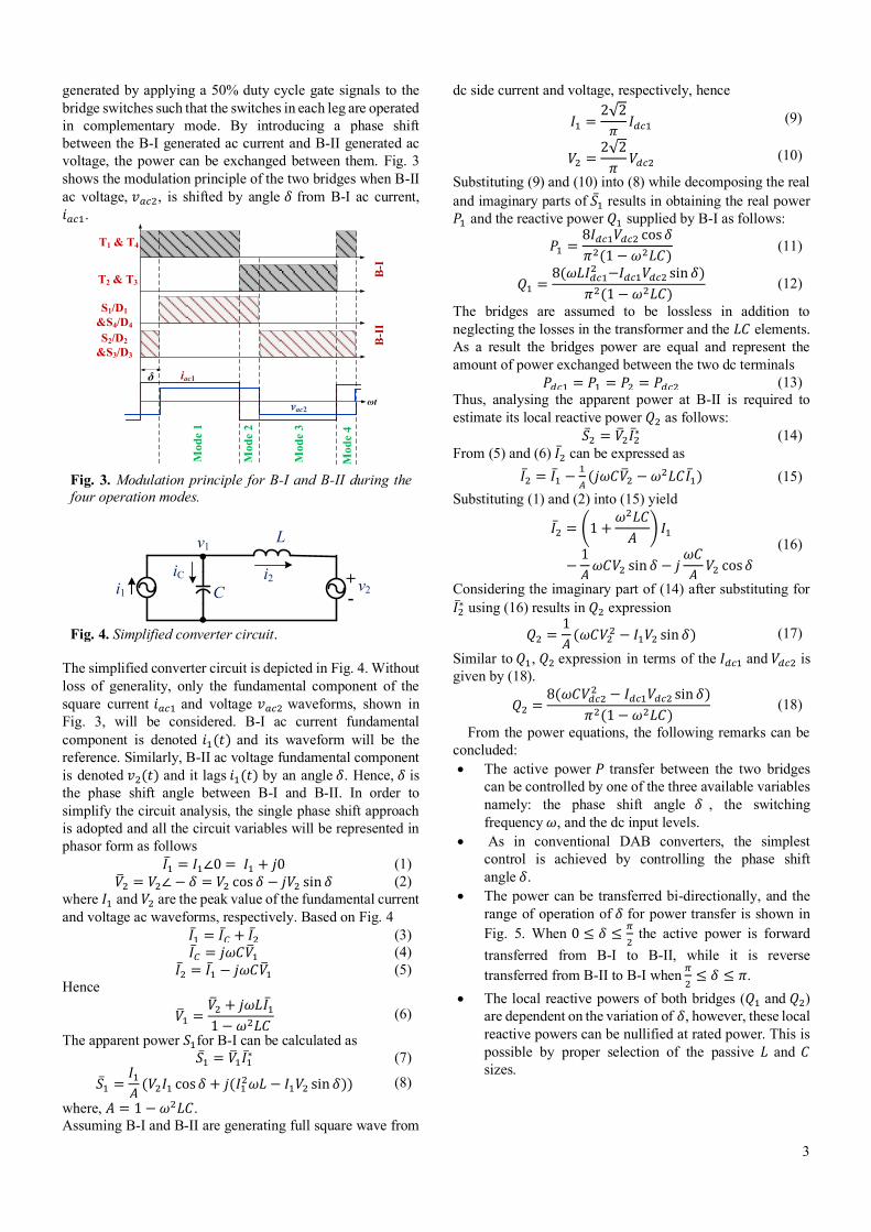
generated by applying a 50% duty cycle gate signals to the
bridge switches such that the switches in each leg are operated
in complementary mode. By introducing a phase shift
between the B-I generated ac current and B-II generated ac
voltage, the power can be exchanged between them. Fig. 3
shows the modulation principle of the two bridges when B-II
ac voltage, 𝑣𝑎𝑐2, is shifted by angle 𝛿 from B-I ac current,
𝑖𝑎𝑐1.
Fig. 3. Modulation principle for B-I and B-II during the
four operation modes.
Fig. 4. Simplified converter circuit.
The simplified converter circuit is depicted in Fig. 4. Without
loss of generality, only the fundamental component of the
square current 𝑖𝑎𝑐1 and voltage 𝑣𝑎𝑐2 waveforms, shown in
Fig. 3, will be considered. B-I ac current fundamental
component is denoted 𝑖1(𝑡) and its waveform will be the
reference. Similarly, B-II ac voltage fundamental component
is denoted 𝑣2(𝑡) and it lags 𝑖1(𝑡) by an angle 𝛿. Hence, 𝛿 is
the phase shift angle between B-I and B-II. In order to
simplify the circuit analysis, the single phase shift approach
is adopted and all the circuit variables will be represented in
phasor form as follows
𝐼1 = 𝐼1∠0 = 𝐼1 + 𝑗0 (1)
2 = 𝑉2∠ − 𝛿 = 𝑉2 cos 𝛿 − 𝑗𝑉2 sin 𝛿 (2)
where 𝐼1 and 𝑉2 are the peak value of the fundamental current
and voltage ac waveforms, respectively. Based on Fig. 4
𝐼1 = 𝐼 + 𝐼2 (3)
𝐼 = 𝑗𝜔𝐶1 (4)
𝐼2 = 𝐼1 − 𝑗𝜔𝐶1 (5)
Hence
1 =2 + 𝑗𝜔𝐿𝐼1
1 − 𝜔2𝐿𝐶 (6)
The apparent power 𝑆1for B-I can be calculated as
1 = 1𝐼1∗ (7)
1 =𝐼1
𝐴(𝑉2𝐼1 cos 𝛿 + 𝑗(𝐼1
2𝜔𝐿 − 𝐼1𝑉2 sin 𝛿)) (8)
where, 𝐴 = 1 − 𝜔2𝐿𝐶.
Assuming B-I and B-II are generating full square wave from
dc side current and voltage, respectively, hence
𝐼1 =2√2
𝜋𝐼𝑑𝑐1 (9)
𝑉2 =2√2
𝜋𝑉𝑑𝑐2 (10)
Substituting (9) and (10) into (8) while decomposing the real
and imaginary parts of 1 results in obtaining the real power
𝑃1 and the reactive power 𝑄1 supplied by B-I as follows:
𝑃1 =8𝐼𝑑𝑐1𝑉𝑑𝑐2 cos 𝛿
𝜋2(1 − 𝜔2𝐿𝐶) (11)
𝑄1 =8(𝜔𝐿𝐼𝑑𝑐1
2 −𝐼𝑑𝑐1𝑉𝑑𝑐2 sin 𝛿)
𝜋2(1 − 𝜔2𝐿𝐶) (12)
The bridges are assumed to be lossless in addition to
neglecting the losses in the transformer and the 𝐿𝐶 elements.
As a result the bridges power are equal and represent the
amount of power exchanged between the two dc terminals
𝑃𝑑𝑐1 = 𝑃1 = 𝑃2 = 𝑃𝑑𝑐2 (13)
Thus, analysing the apparent power at B-II is required to
estimate its local reactive power 𝑄2 as follows:
2 = 2𝐼2∗ (14)
From (5) and (6) 𝐼2 can be expressed as
𝐼2 = 𝐼1 −1
𝐴(𝑗𝜔𝐶2 − 𝜔2𝐿𝐶𝐼1) (15)
Substituting (1) and (2) into (15) yield
𝐼2 = (1 +𝜔2𝐿𝐶
𝐴) 𝐼1
−1
𝐴𝜔𝐶𝑉2 sin 𝛿 − 𝑗
𝜔𝐶
𝐴𝑉2 cos 𝛿
(16)
Considering the imaginary part of (14) after substituting for
𝐼2∗ using (16) results in 𝑄2 expression
𝑄2 =1
𝐴(𝜔𝐶𝑉2
2 − 𝐼1𝑉2 sin 𝛿) (17)
Similar to 𝑄1, 𝑄2 expression in terms of the 𝐼𝑑𝑐1 and 𝑉𝑑𝑐2 is
given by (18).
𝑄2 =8(𝜔𝐶𝑉𝑑𝑐2
2 − 𝐼𝑑𝑐1𝑉𝑑𝑐2 sin 𝛿)
𝜋2(1 − 𝜔2𝐿𝐶) (18)
From the power equations, the following remarks can be
concluded:
• The active power 𝑃 transfer between the two bridges
can be controlled by one of the three available variables
namely: the phase shift angle 𝛿 , the switching
frequency 𝜔, and the dc input levels.
• As in conventional DAB converters, the simplest
control is achieved by controlling the phase shift
angle 𝛿.
• The power can be transferred bi-directionally, and the
range of operation of 𝛿 for power transfer is shown in
Fig. 5. When 0 ≤ 𝛿 ≤𝜋
2 the active power is forward
transferred from B-I to B-II, while it is reverse
transferred from B-II to B-I when 𝜋
2≤ 𝛿 ≤ 𝜋.
• The local reactive powers of both bridges (𝑄1 and 𝑄2)
are dependent on the variation of 𝛿, however, these local
reactive powers can be nullified at rated power. This is
possible by proper selection of the passive 𝐿 and 𝐶
sizes.
ωt
δ iac1
vac2
T1 & T4
T2 & T3
S1/D1
&S4/D4
Mod
e 1
Mo
de 2
Mod
e 3
Mod
e 4
S2/D2
&S3/D3
B-I
B-I
I
L
Ci1
+
-
iC
v1
i2v2

4
Fig. 5. Variation of phase shift angle and power exchanged
between the two bridges.
2.2. Operation Principal
The phase shift angle controls the power flow direction,
accordingly the LCC and the VSC will adjust the suitable
polarity for their 𝑉𝑑𝑐1 and 𝐼𝑑𝑐2, respectively. Therefore, the
corresponding switching pattern must be used to facilitate the
required power follow through B-I and B-II switches.
Assuming the current and the voltage polarities shown in Fig.
2a are positive, there will be 4 modes of operation (see Fig. 3)
at forward power as well as at reverse power.
During forward power flow (power from B-I to B-II), the
circuit configurations and the active switches are illustrated
in Fig. 6. Since 𝐼𝑑𝑐2 is negative in B-II, the antiparallel diodes
𝐷𝑖 operate and the switches 𝑆𝑖 are switched OFF. In contrast,
during reverse power flow (power from B-II to B-I), 𝐼𝑑𝑐2 is
positive in B-II, therefore, the switches 𝑆𝑖 operate and the
diodes 𝐷𝑖 are OFF. The circuit configuration and the active
switches at reverse power are illustrated in Fig. 7. It is also
clear that in both power flow conditions B-I switches
𝑇𝑖 operated to generate the ac current waveform, since 𝐼𝑑𝑐1
has fixed positive polarity. But, the dc voltage 𝑉𝑑𝑐1 has
negative polarity in reverse power mode, therefore, reverse
blocking capability is needed for B-I switches.
(a) (b)
(c) (d)
Fig. 6. Proposed dc-dc converter circuit configuration during forward power flow. (a) Mode 1.
(b) Mode 2. (c) Mode 3. (d) Mode 4.
(a) (b)
(c) (d)
Fig. 7. Proposed dc-dc converter circuit configuration during reverse power flow. (a) Mode 1.
(b) Mode 2. (c) Mode 3. (d) Mode4.
δ
P
0
Pmax
-Pmax
π/2 π
I II
I IIP
P
S1
S2 S4
S3
L
C
Idc2
Vdc2
Bridge I Bridge II
vac2
1: n
VS
C-H
VD
C
iac2
Mode 1
D1 D3
D2 D4
T1
T2 T4
T3
Idc1
Vdc1
iac1
LC
C-H
VD
C
vac1
S1
S2 S4
S3
T1
T2 T4
T3
L
C
Idc1
Vdc1
Idc2
Vdc2
Bridge I Bridge II
vac2
iac1
1: n L
CC
-HV
DC
VS
C-H
VD
C
iac2
vac1
Mode 2
D1 D3
D2 D4
S1
S2
T1
T2 T4
T3
L
C
Idc1
Vdc1
Bridge I
iac1
1: n
LC
C-H
VD
C
vac1
Mode 3
S4
S3
Idc2
Vdc2
Bridge II
vac2
VS
C-H
VD
C
iac2
D1 D3
D2 D4
S1
S2 S4
S3
T1
T2 T4
T3
L
C
Idc1
Vdc1
Idc2
Vdc2
Bridge I Bridge II
vac2
iac1
1: n
LC
C-H
VD
C
VS
C-H
VD
C
iac2
vac1
Mode 4
D1 D3
D2 D4
S1
S2 S4
S3
L
C
Idc2
Vdc2
Bridge I Bridge II
vac2
1: n
VS
C-H
VD
C
iac2
Mode 1
D1 D3
D2 D4
T1
T2 T4
T3
Idc1
Vdc1
iac1
LC
C-H
VD
C
vac1
S1
S2 S4
S3
L
C
Idc2
Vdc2
Bridge I Bridge II
vac2
1: n
VS
C-H
VD
C
iac2
Mode 2
D1 D3
D2 D4
T1
T2 T4
T3
Idc1
Vdc1
iac1
LC
C-H
VD
C
vac1
S1
S2 S4
S3
L
C
Idc2
Vdc2
Bridge I Bridge II
vac2
1: n
VS
C-H
VD
C
iac2
Mode 3
D1 D3
D2 D4
T1
T2 T4
T3
Idc1
Vdc1
iac1
LC
C-H
VD
C
vac1
S1
S2 S4
S3
L
C
Idc2
Vdc2
Bridge I Bridge II
vac2
1: n
VS
C-H
VD
C
iac2
Mode 4
D1 D3
D2 D4
T1
T2 T4
T3
Idc1
Vdc1
iac1
LC
C-H
VD
C
vac1

5
2.3. Parameters selection
As aforementioned, the key factor for the 𝐿𝐶 selection is to
nullify the local reactive powers at the converter rated active
power. Normally, nullifying 𝑄1 at the rated power will result
in the design equation of 𝐿 while 𝐶 design equation is
obtained from nullifying 𝑄2. Hence, the design equations for
𝐿 and 𝐶 can be obtained from nullifying (12) and (18), thus
𝐿 =𝑉𝑑𝑐2 sin 𝛿
𝜔𝐼𝑑𝑐1
(19)
𝐶 =𝐼𝑑𝑐1 sin 𝛿
𝜔𝑉𝑑𝑐2
(20)
It is recommended that the calculated values of 𝐿 and 𝐶 are obtained at the rated converter active power. Varying the
phase shift angle 𝛿 will directly vary the size of 𝐿𝐶 elements
required to nullify the local reactive powers.
Fig. 8 shows the active and reactive powers exchange with
𝛿 variation, 0 ≤ 𝛿 ≤ 180° . The rated active power is
assumed to be transferred at 𝛿 = 10°. It can be seen that, at
𝛿 = 10° the reactive powers at B-I and B-II are zero.
Additionally, the power is positive at B-I and negative at B-
II as expected. Varying 𝛿 leads to a corresponding change in
the transferred active power according to (11) with non-zero
reactive powers according to (12) and (18). Fig. 8 illustrates
the potential of the proposed topology to have zero voltage
switching (ZVS) and zero current switching (ZCS). If local
reactive powers ( 𝑄1 and 𝑄2 ) are nullified at rated power,
current will be in phase with voltage, therefore essentially
ZVS and ZCS switching both will be achieved. When the
power is reduced below the rated power ZVS or ZCS will be
achieved depending on the nature of reactive power flow (capacitive or inductive). ZVS is possible with local reactive
power at bridge being inductive. ZCS is possible with local
reactive power at bridge being capacitive.
Fig. 9 parts a and b show the per-unit (pu) variation of the
𝐿 and 𝐶 with 𝛿 , respectively, based on the parameters in
Table 1. It can be seen that as 𝛿 increases the 𝐿𝐶 sizes also
increase. Selecting the appropriate 𝛿 for rated power transfer
is a tradeoff between the passive component sizes and the
required control range. Although the reactive power is not
nullified at all loading conditions, this does not necessitate a derating for the bridges switching devices. At the design stage
the switches selection should be based on the maximum
active and maximum reactive powers that is
𝑃𝑚𝑎𝑥 =8𝐼𝑑𝑐1𝑉𝑑𝑐2
𝜋2(1 − 𝜔2𝐿𝐶) (21)
𝑄𝑚𝑎𝑥 =8(𝜔𝐿𝐼𝑑𝑐1
2 +𝐼𝑑𝑐1𝑉𝑑𝑐2)
𝜋2(1 − 𝜔2𝐿𝐶) (22)
Fig. 8. Per unit variation of active and reactive powers at
B-I and B-II with the phase shift angle 𝛿 °.
3. Power Transfer Simulation Results
The proposed dc-dc converter topology is assessed using
MATLAB/Simulink simulations, with the parameters given
in Table 1. The ac-link inductance and capacitance are
calculated based on (19) and (20), respectively. The obtained
inductance value under rated conditions from (19) is 𝐿 =92mH. Hence, an inductance of 89.3mH is added in addition
to the ac-link transformer leakage inductance.
Table 1 Simulation Specifications Rated power (base power) 𝑃𝑟 410MW
LCC dc current level (base current) 𝐼𝑑𝑐1 1000A
VSC dc Voltage level 𝑉𝑑𝑐2 500kV
ac link frequency 𝑓𝑠 150Hz
Phase-shift angle at forward rated power 𝛿 10º
ac link transformer
Rated
power 500MVA
N1/N2 1
Leakage
impedance 50+j2.7mΩ
ac link inductance 𝐿 89.3mH
ac link capacitance 𝐶 0.37μF
(a)
(b)
Fig. 9. Per unit 𝐿𝐶 size variation with the phase shift
angle 𝛿 °. (a) Inductance. (b) Capacitance.
The pu values are calculated by considering the base power
is the rated power and B-I dc current is the base current. Fig.
10 shows the forward (from B-I to B-II) and reverse (from B-
II to B-I) power transfer at rated as well as partial loading
conditions. The power transfer profile is detailed as follows:
• From 𝑡 = 0 to 𝑡 = 0.25s, converter is operating at full
rated power in forward direction.
• From 𝑡 = 0.25s to 𝑡 = 0.5s, converter is operating with
0.5𝑃𝑟 in in forward direction.
• From 𝑡 = 0.5s to 𝑡 = 0.75s, converter is operating with
0.5𝑃𝑟 in reverse direction.
• From 𝑡 = 0.75s to 𝑡 = 1.0s, converter is operating with
full rated power in reverse direction.
0 10 20 30 40 50 60 70 80 900
0.2
0.4
0.6
0.8
1
1.2
1.4x 10
-3
Ind
ucta
nce, p
u
0 10 20 30 40 50 60 70 80 900
0.5
1
1.5
2
x 10-6
Ca
pa
cit
an
ce, p
u

6
It can be shown in Fig. 10a and Fig. 10b that the active power
is transferred, in both directions, with zero local reactive
power. As illustrated in Fig. 5, in order to reverse the power
from B-II to B-I while keeping the reactive powers nullified;
the phase shift angle is increased to 𝛿 = 170° instead of 𝛿 =10° in the forward power transfer case. Moreover, the dc link
currents and voltages at bridges terminals are depicted in Fig. 10 parts c and d for B-I and B-II, respectively. As expected,
B-I current is always kept fixed while its dc link voltage is
varied. In contrast, the dc link voltage of B-II is fixed while
its dc current varied. Transferring the partial power will
encounter some reactive power transfer as expected. Fig. 11
shows the phase-shift angle variation between the ac link
current 𝑖𝑎𝑐1 of B-I and the ac voltage 𝑣𝑎𝑐2 of B-II.
Corresponding to the previously mentioned loading
conditions, at forward rated power 𝛿 = 10° as in Fig. 11a,
while at 0.5𝑃𝑟 it is increased to 𝛿 = 61.4° as illustrated in
Fig. 11b. Similarly, in reverse power mode 𝛿 = 118.6° and
𝛿 = 170° for 𝑃𝑟 and 0.5𝑃𝑟 as shown in Fig. 11c and Fig. 11d,
respectively.
(a) (b)
(c) (d)
Fig. 10. Simulation results for power exchange between B-I and B-II. (a) Active and reactive
powers at B-I (b) Active and reactive powers at B-II. (c) dc link voltage and current at B-I. (d)
dc link voltage and current at B-II.
(a) (b)
(c) (d)
Fig. 11. Simulation results for phase-shift angle between B-I ac link current and B-II ac link
voltage. (a) When forward rated power is transferred (from B-I to B-II). (b) When forward half-
rated power is transferred (from B-I to B-II). (c) When reverse half-rated power is transferred
(from B-II to B-I). (d) When reverse rated power is transferred (from B-II to B-I).
0 0.2 0.4 0.6 0.8 1
-1
-0.5
0
0.5
1
Time, s
B-I
Acti
ve a
nd
Rea
cti
ve P
ow
ers,
pu
P1
Q1
0 0.2 0.4 0.6 0.8 1
-1
-0.5
0
0.5
1
Time, s
B-I
I A
cti
ve a
nd
Rea
cti
ve P
ow
ers,
pu
P2
Q2
0 0.2 0.4 0.6 0.8 1
-1
-0.5
0
0.5
1
Time, s
B-I
DC
vo
lta
ge a
nd
DC
cu
rren
t, p
u
Idc1
Vdc1
0 0.2 0.4 0.6 0.8 1-1
-0.5
0
0.5
1
1.5
Time, s
B-I
I D
C v
olt
ag
e a
nd
DC
cu
rren
t, p
u
Idc2
Vdc2
0 0.002 0.004 0.006 0.008 0.01 0.012-1.5
-1
-0.5
0
0.5
1
1.5
Time, s
B-I
AC
cu
rren
t a
nd
B-I
I A
C v
olt
ag
e, p
u = 10
Iac1
Vac2
0 0.002 0.004 0.006 0.008 0.01 0.012-1.5
-1
-0.5
0
0.5
1
1.5
Time, s
B-I
AC
cu
rren
t a
nd
B-I
I A
C v
olt
ag
e, p
u = 61.4
Iac1
Vac2
0 0.002 0.004 0.006 0.008 0.01 0.012-1.5
-1
-0.5
0
0.5
1
1.5
Time, s
B-I
AC
cu
rren
t a
nd
B-I
I A
C v
olt
ag
e, p
u = 118.6
Iac1
Vac2
0 0.002 0.004 0.006 0.008 0.01 0.012-1.5
-1
-0.5
0
0.5
1
1.5
Time, s
B-I
AC
cu
rren
t a
nd
B-I
I A
C v
olt
ag
e, p
u = 170
Iac1
Vac2

7
4. Power Transfer Experimental Results
In order to demonstrate the proposed converter practically,
a scaled-down experimental set-up is implemented with the
specifications listed in Table 2. A stiff LCC is adopted and an
ac inductor is used instead of a transformer. The experimental
schematic diagram is shown in Fig. 12. Bridge B-I needs
reverse-blocking switches; this can be achieved by utilising
IGCTs or by using an IGBT in series with a diode. Such
approach is widely used in MV drives [26] and wind energy
conversion converters [27] and is adopted here instead of the
IGCTs for B-I. The VSC side is emulated by a dc voltage source feeding B-II (see Fig. 12). The LCC side is emulated by a
dedicated circuit and control (see Fig. 12) according to the
power flow direction: • For forward power flow (from B-I to B-II) switches FB1
and FB4 are ON while FB2, FB3 and SW2 are OFF. The dc-
link current is regulated by a PI controller, which
generates the duty-cycle of SW1. The switch SW1 operates
only in forward power flow.
• For reverse power flow (from B-II to B-I) FB2 and FB3 are
ON while FB1, FB4 and SW1 are OFF. SW2 duty-cycle will
be controlled by the PI controller to keep the converter
current constant. The switch SW2 operates only in reverse
power flow. In reverse power flow, a power resistor is
added in series with SW2 to absorb the power.
Table 2 Experimental Specifications
Proposed Topology Parameters and Active Components
Rated power (base power) 𝑃𝑟 400W
LCC dc current level (base
current) 𝐼𝑑𝑐1 60A
VSC dc Voltage level 𝑉𝑑𝑐2 80V
ac link frequency 𝑓𝑠 150Hz
Phase-shift angle at forward
rated power 𝛿 10º
ac link inductance 𝐿 2.5mH
ac link capacitance 𝐶 13.8μF
B-II active IGBT switches part
No. 𝑆𝑖 IHW30N160R2FKSA1
B-I active switches part No.
(IGBT in series with Diode) 𝑇𝑖
IHW30N160R2FKSA1
and
DSEI30-10A
Stiff Current Source Generator Parameters and Active
Components
dc input voltage level 150V
IGBT switches SW1 and SW2
part No. IGW60T120FKSA1
Input power resistor 5Ω, 750W
Voltage reversal bridge IGBT
switches FBi part No. IGW60T120FKSA1
dc-link inductance 100mH
Fig. 12. Schematic diagram for the experimental set-up.
The power transfer profile is detailed in normal operation as
follows:
• From 𝑡 = 0 to 𝑡 = 2.5 s, converter is operating at full
rated power in forward direction.
• From 𝑡 = 2.5 s to 𝑡 = 5 s, converter is operating with
0.5𝑃𝑟 in in forward direction.
• From 𝑡 = 5 s to 𝑡 = 7.5 s, converter is operating with
0.5𝑃𝑟 in reverse direction.
• From 𝑡 = 7.5s to 𝑡 = 10s, converter is operating with full
rated power in reverse direction.
The obtained results are given in Fig. 13. Fig. 13 parts a and b
show the dynamic power transfer between B-I and B-II
according to the aforementioned power profile in normal
operation. It can be seen that, regardless the power direction, B-
I dc-current is fixed at 6A while B-II dc voltage is fixed at 80V
while the dc voltage and the dc current of B-I and B-II
respectively are varied to comply with the power transfer
amount and direction. For forward power transfer, the phase
angle shift between the ac current and the ac voltage of B-I and
B-II respectively is 𝛿 = 10° , as shown in Fig. 13c. Also,
reverse power transfer is evident at 𝛿 = 170°, as shown in Fig.
13d. Moreover, for 0.5𝑃𝑟 transfer in the forward direction the
phase shift angle is adjusted at 𝛿 = 60° as depicted in Fig. 13e.
Therefore, by adjusting the phase-shift angle not only the
amount of power transfer is controlled, but its direction as well.
S1
S2 S4
S3
T1
T2 T4
T3
L
C
Idc1
Vdc1
Idc2
Vdc2
Bridge I Bridge II
vac2iac1
-
SW1 SW2 FB1
FB2
FB3
FB4
Ldc
150 V
-
Idc1
5
+-Idc1_ref
PI
PWM
Carrier
Idc1
SW1 (forward power) &
SW2 (reverse power)
LCC Emulator Controller
LCC Emulator
Proposed DABV
SC
Em
ula
tor

8
(a) (b)
(c) (d)
(e)
Fig. 13. Experimental results in normal operation power profile. (a) B-I active power, dc link current and dc
voltage. (b) B-II active power, dc link current and dc voltage.(c) B-I ac current and B-II ac voltage at 𝛿 = 10°.
(d) B-I ac current and B-II ac voltage at 𝛿 = 170°. (e) B-I ac current and B-II ac voltage at 𝛿 = 60°.
5. Simulating The Proposed Converter Response During DC-DC Faults
The response of the proposed converter topology to the dc
link pole-to-pole faults is studied without any additional
control action or hardware modification. Two scenarios are
adopted as illustrated in Fig. 14, when the fault occurs at B-I
and B-II dc links when receiving the rated power from the
other bridge terminal. In the first scenario, the rated power is
transferred to B-I when a dc pole-to-pole fault occurred at the
B-I dc-link at 𝑡 = 0.15s as shown in Fig. 15. During the fault,
B-I dc link voltage reduced to zero (or closer to zero
depending on the fault resistance). Hence the received active
power is nullified as shown in Fig. 15 parts a and b. B-I dc
link current is fixed at its rated value similar to B-II voltage
as shown in Fig. 15 parts c and d. Additionally, during the
fault, some reactive power is evident since the passive
elements are feeding the fault. After the fault is cleared at
𝑡 = 0.25s, the pre-fault operation is restored and the reactive
power is nullified.
Similarly in the second scenario depicted in Fig. 16, a dc
pole to pole fault occurred at B-II at 𝑡 = 0.15 s when receiving the rated power from B-I. Immediately the dc
voltage at B-II is dropped to zero, hence as seen in Fig. 16
parts a and b during the fault the active power sent from B-I
dropped to zero while the B-II dc current is limited to the
rated current, see Fig. 16d. The dc link voltage at B-I is
dropped to zero while the dc link current is fixed at its rated
value as shown in Fig. 16c.
Fig. 14. Applied fault scenarios to study the proposed
converter response.
Ref
Idc1
Vdc1
Time: 1s/div.
Current: 2 A/div.
Voltage: 40 V/div.
Power: 100 W/div.
P1
RefIdc2
Vdc2
Time: 1s/div.
Current: 2 A/div.
Voltage: 40 V/div.
Power: 100 W/div.
P2
Ref
Vac2
Time: 2ms/div.
Current: 2 A/div.
Voltage: 20 V/div.
Iac1
Ref
Vac2
Time: 2ms/div.
Current: 2 A/div.
Voltage: 20 V/div.
Iac1
Ref
Vac2
Time: 2ms/div.
Current: 2 A/div.
Voltage: 20 V/div.
Iac1
B-I B-II1: n
Scenario 1
~~ ==
Scenario 2
LC
C-H
VD
C
VS
C-H
VD
C

9
(a) (b)
(c) (d)
Fig. 15. Simulation results for dc pole to pole fault at B-I when receiving rated power from B-II. (a) Active and reactive
powers at B-I (b) Active and reactive powers at B-II. (c) dc link voltage and current at B-I. (d) dc link voltage and current
at B-II.
(a) (b)
(c) (d)
Fig. 16. Simulation results for dc pole to pole fault at B-II when receiving rated power from B-I. (a) Active and reactive
powers at B-I (b) Active and reactive powers at B-II. (c) dc link voltage and current at B-I. (d) dc link voltage and current
at B-II.
6. Proposed Converter Discussion and Topology Variations
As illustrated in Fig. 2b, the proposed topology can be
extended to three-phase in order to allow bulk power transfer.
To simplify the analysis in this paper, rectangular ac waveforms
are considered. Therefore, high 𝑑𝑖/𝑑𝑡 and 𝑑𝑣/𝑑𝑡 will be
encountered at the LCC and the VSC sides, respectively. On the
other hand, the capacitor at the LCC side and the inductor at the
VSC side will result in nicer 𝑑𝑣/𝑑𝑡 and 𝑑𝑖/𝑑𝑡, respectively.
However, a trapezoidal waveform can be adopted for the ac
current and the ac voltage generated across the inner LC link.
Such waveform will further reduce the 𝑑𝑣/𝑑𝑡 generated across the transformer by utilising conventional Modular Multilevel
Converter Sub-Modules (MMC-SMs), the Half-Bridge (HB)
and the Full-Bridge (FB) types as in Fig. 17a. In trapezoidal
modulation, the utilised MMC-SMs are inserted during the
transition from positive to negative dc rails and vice-versa [11].
Additionally, applying the Transition Arm Converter (TAC)
concept is viable, as illustrated in Fig. 17b. In TAC the lower
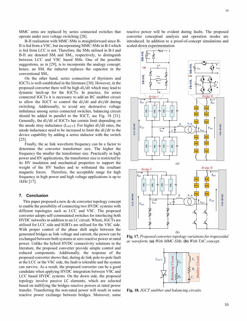
10
10
MMC arms are replaced by series connected switches that
operate under zero voltage switching [28].
B-II realisation with MMC-SMs is straightforward since B-II is fed from a VSC, but incorporating MMC-SMs in B-I which
is fed from LCC is not. Therefore, the SMs utilised in B-I and
B-II are denoted SMi and SMv, respectively, to distinguish
between LCC and VSC based SMs. One of the possible
suggestions, as in [29], is to incorporate the analogy concept;
hence, an SMi the inductor replaces the capacitor in the
conventional SMv.
On the other hand, series connection of thyristors and
IGCTs is well-established in the literature [30]. However, in the
proposed converter there will be high 𝑑𝑖/𝑑𝑡 which may lead to
dynamic latch-up for the IGCTs. In practice, for series connected IGCTs it is necessary to add an RC snubber circuit
to allow the IGCT to control the 𝑑𝑖/𝑑𝑡 and 𝑑𝑣/𝑑𝑡 during
switching. Additionally, to avoid any destructive voltage
imbalance among series connected switches, balancing circuit
should be added in parallel to the IGCT, see Fig. 18 [31].
Generally, the 𝑑𝑖/𝑑𝑡 of IGCTs has certain limit depending on
the anode stray inductance (LIGCT). For higher 𝑑𝑖/𝑑𝑡 rates, the
anode inductance need to be increased to limit the 𝑑𝑖/𝑑𝑡 to the device capability by adding a series inductor with the switch
[25].
Finally, the ac link waveform frequency can be a factor to
determine the converter transformer size. The higher the
frequency the smaller the transformer size. Practically in high
power and HV applications, the transformer size is restricted by
its HV insulation and mechanical properties to support the
weight of the HV bushes and to withstand the resultant
magnetic forces. Therefore, the acceptable range for high
frequency in high power and high voltage applications is up to
1kHz [17].
7. Conclusion
This paper proposed a new dc-dc converter topology concept
to enable the possibility of connecting two HVDC systems with
different topologies such as LCC and VSC. The proposed
converter adopts self-commutated switches for interfacing both HVDC networks in addition to an LC circuit. Where, IGCTs are
utilised for LCC side and IGBTs are utilised for the VSC side.
With proper control of the phase shift angle between the
generated bridges ac link voltage and current, the power can be
exchanged between both systems at zero reactive power at rated
power. Unlike the hybrid HVDC connectivity solutions in the
literature, the proposed converter provide simple control and
reduced components. Additionally, the response of the
proposed converter shows that, during dc link pole-to-pole fault
at the LCC or the VSC side, the fault is tolerable and the system
can survive. As a result, the proposed converter can be a good
candidate when applying HVDC integration between VSC and LCC based HVDC systems. On the down side, the proposed
topology involve passive 𝐿𝐶 elements, which are selected
based on nullifying the bridges reactive powers at rated power
transfer. Transferring the non-rated power will result in some
reactive power exchange between bridges. Moreover, some
reactive power will be evident during faults. The proposed
converter conceptual analysis and operation modes are
introduced. In addition to a proof-of-concept simulations and scaled-down experimentation.
(a)
(b)
Fig. 17. Proposed converter topology variations for trapezoidal
ac waveform. (a) With MMC-SMs. (b) With TAC concept.
Fig. 18. IGCT snubber and balancing circuits.
Vdc1
Idc2
Vdc2
Bridge II
SMv
L
C vac2iac1
1: n
SMv
SMvSMv
SMv SMv
SMvSMv
SMvSMv
SMv SMv
A
B
ISM
LSM
VS
C-H
VD
C
A
B
CSM
+
-VSM
+
-
CSM
+
-
A
B
VSM
+
-
FB
-SM
iH
B-S
Mi
HB
-SM
vF
B-S
Mv
LC
C-H
VD
C
OR
OR
Bridge I
Idc1
SM
i
SM
i
SM
i
SM
i
SM
i
SM
i
SM
i
SM
i
LSM
ISM
B
A
Vdc1
Idc2
Vdc2
Bridge IBridge II
C vac2iac1
SMv SMv
SMv
SMvSMv
SMv
L 1: n
VS
C-H
VD
C
Idc1
SM
i
SM
i
SM
i
SM
i
LC
C-H
VD
C
LIGCT
Cs
Rs
LsLb
Rb Sn
ub
ber
Cir
cuit
Bala
nci
ng C
ircu
it

11
11
8. References
[1] N. Flourentzou, V. G. Agelidis, and G. D. Demetriades, "VSC-based
HVDC power transmission systems: An overview," IEEE Trans.
Power Electron., vol. 24, no. 3, pp. 592-602, 2009.
[2] A. Egea-Alvarez, F. Bianchi, A. Junyent-Ferre, G. Gross, and O.
Gomis-Bellmunt, "Voltage control of multiterminal VSC-HVDC
transmission systems for offshore wind power plants: Design and
implementation in a scaled platform," IEEE Trans. Ind. Electron.,
vol. 60, no. 6, pp. 2381-2391, 2013.
[3] D. Van Hertem and M. Ghandhari, "Multi-terminal vsc hvdc for the
european supergrid: Obstacles," Renewable and Sustainable Energy
Reviews, vol. 14, no. 9, pp. 3156-3163, 2010.
[4] A. Lesnicar and R. Marquardt, "An innovative modular multilevel
converter topology suitable for a wide power range," in IEEE
Bologna Power Tech Conference Proceedings, 2003.
[5] Barker et al., HVDC: Connecting to the Future. Paris, France:
Alstom Grid, 2010.
[6] R. E. Torres-Olguin, M. Molinas, and T. Undeland, "Offshore wind
farm grid integration by VSC technology with LCC-based HVDC
transmission," IEEE Trans. Sustainable Energy, vol. 3, no. 4, pp.
899-907, 2012.
[7] D. Jovcic and J. Zhang, "High power IGBT-based dc/dc converter
with dc fault tolerance," in 15th International Power Electronics
and Motion Control Conference (EPE/PEMC), 2012.
[8] R. W. A. A. D. Doncker, D. M. Divan, and M. H. Kheraluwala, "A
three-phase soft-switched high-power-density dc/dc converter for
high-power applications," IEEE Trans. Ind. Applicat., vol. 27, no. 1,
pp. 63-73, 1991.
[9] A. A. Elserougi, A. Massoud, I. Abdelsalam, and S. Ahmed, "A self-
balanced bidirectional medium-/high-voltage hybrid modular dc–dc
converter with low-voltage common dc-link and sequential
charging/discharging of submodules capacitors," IEEE Trans. Ind.
Electron., vol. 66, no. 4, pp. 2714-2725, 2019.
[10] X. Xiang, X. Zhang, T. Luth, M. M. C. Merlin, and T. C. Green, "A
compact modular multilevel dc–dc converter for high step-ratio mv
and HV use," IEEE Trans. Ind. Electron., vol. 65, no. 9, pp. 7060-
7071, 2018.
[11] A. Gowaid, G. P. Adam, A. M. Massoud, S. Ahmed, D. Holliday,
and B. W. Williams, "Quasi two-level operation of modular
multilevel converter for use in a high-power dc transformer with dc
fault isolation capability," IEEE Trans. Power Electron., vol. 30, no.
1, pp. 108-123, 2015.
[12] B. Zhao, Q. Song, W. Liu, and Y. Sun, "Overview of dual-active-
bridge isolated bidirectional dc–dc converter for high-frequency-
link power-conversion system," IEEE Trans. Power Electron., vol.
29, no. 8, pp. 4091-4106, 2014.
[13] G. P. Adam, K. H. Ahmed, S. J. Finney, K. Bell, and B. W. Williams,
"New breed of network fault-tolerant voltage-source-converter
HVDC transmission system," IEEE Trans. Power Syst., vol. 28, no.
1, pp. 335-346, 2013.
[14] K. H. Ahmed, G. P. Adam, I. A. Abdelsalam, and A. A. Aboushady,
"Modular multilevel converter with modified half-bridge
submodule and arm filter for dc transmission systems with dc fault
blocking capability," IET Power Electronics, vol. 11, no. 14, pp.
2253-2262, 2018.
[15] D. Jovcic, "Bidirectional, high-power dc transformer," IEEE Trans.
Power Delivery, vol. 24, no. 4, pp. 2276-2283, 2009.
[16] D. Jovcic and B. T. Ooi, "Developing dc transmission networks
using dc transformers," IEEE Trans. Power Delivery, vol. 25, no. 4,
pp. 2535-2543, 2010.
[17] G. P. Adam, I. A. Gowaid, S. J. Finney, D. Holliday, and B. W.
Williams, "Review of dc–dc converters for multi-terminal HVDC
transmission networks," IET Power Electronics, vol. 9, no. 2, pp.
281-296, 2016.
[18] S. P. Engel, M. Stieneker, N. Soltau, S. Rabiee, H. Stagge, and R.
W. D. Doncker, "Comparison of the modular multilevel dc
converter and the dual-active bridge converter for power conversion
in hvdc and mvdc grids," IEEE Trans. Power Electron., vol. 30, no.
1, pp. 124-137, 2015.
[19] J. D. Páez, D. Frey, J. Maneiro, S. Bacha, and P. Dworakowski,
"Overview of dc–dc converters dedicated to hvdc grids," IEEE
Trans. Power Delivery, vol. 34, no. 1, pp. 119-128, 2019.
[20] R. E. Torres-Olguin, A. Garces, M. Molinas, and T. Undeland,
"Integration of offshore wind farm using a hybrid hvdc transmission
composed by the pwm current-source converter and line-
commutated converter," IEEE Trans. Energy Conversion, vol. 28,
no. 1, pp. 125-134, 2013.
[21] M. Hajian, J. Robinson, D. Jovcic, and B. Wu, "30 kW, 200 V/900
V, Thyristor LCL DC/DC Converter Laboratory Prototype Design
and Testing," IEEE Trans. Power Electron., vol. 29, no. 3, pp. 1094-
1102, 2014.
[22] P. Li, G. P. Adam, S. J. Finney, and D. Holliday, "Operation
Analysis of Thyristor-Based Front-to-Front Active-Forced-
Commutated Bridge DC Transformer in LCC and VSC Hybrid
HVDC Networks," IEEE Journal of Emerging and Selected Topics
in Power Electronics, vol. 5, no. 4, pp. 1657-1669, 2017.
[23] Z. Yang, M. Li, X. Lu, W. Xiang, W. Zuo, L. Yao, et al.,
"Interconnection of VSC-HVDC and LCC-HVDC using DC–DC
autotransformer," The Journal of Engineering, vol. 2019, no. 18, pp.
5033-5037, 2019.
[24] R. Zeng, B. Zhao, T. Wei, C. Xu, Z. Chen, J. Liu, et al., "Integrated
gate commutated thyristor-based modular multilevel converters: A
promising solution for high-voltage dc applications," IEEE Ind.
Electron. Mag., vol. 13, no. 2, pp. 4-16, 2019.
[25] B. Zhao, R. Zeng, Z. Yu, Q. Song, Y. Huang, Z. Chen, et al., "A
more prospective look at igct: Uncovering a promising choice for dc
grids," IEEE Ind. Electron. Mag., vol. 12, no. 3, pp. 6-18, 2018. [26] M. A. Elgenedy, A. A. Elserougi, A. S. Abdel-Khalik, A. M.
Massoud, and S. Ahmed, "A Space Vector PWM Scheme for Five-
Phase Current-Source Converters," IEEE Trans. Ind. Electron., vol.
63, no. 1, pp. 562-573, 2016. [27] M. A. Elgenedy, A. S. Abdel-Khalik, A. A. Elserougi, S. Ahmed
and A. Massoud, “A Current-Source-Converter-Based PMSG Wind
Energy Conversion System: Simulation Study,” 15th International
Middle East Power System Conference (MEPCON), 2012. [28] I. A. Gowaid, G. P. Adam, B. W. Williams, A. M. Massoud, S.
Ahmed, "The transition arm multilevel converter — A concept for
medium and high voltage DC-DC transformers," International
Conference on Industrial Technology (ICIT), 2015.
[29] A. Nami, J. Liang, F. Dijkhuizen, and G. D. Demetriades, "Modular
Multilevel Converters for HVDC Applications: Review on
Converter Cells and Functionalities," IEEE Trans. Power Electron.,
vol. 30, no. 1, pp. 18-36, 2015.
[30] B. Wu, High Power Converter Systems. Piscataway, NJ, USA:
IEEE Press, 2006.
[31] Z. Zhao, L. Yuan, H. Bai, and T. Lu, Electromagnetic Transients of
Power Electronics Systems: Springer, 2019.


