
Digital System Basics
Logic GatesLogic gates are the basic building blocks of any digital system. It is an electronic circuit having one or more than one input and only one output. The relationship between the input and the output is based on a certain logic. Based on this logic gates are named as AND gate, OR gate, NOT gate etc.
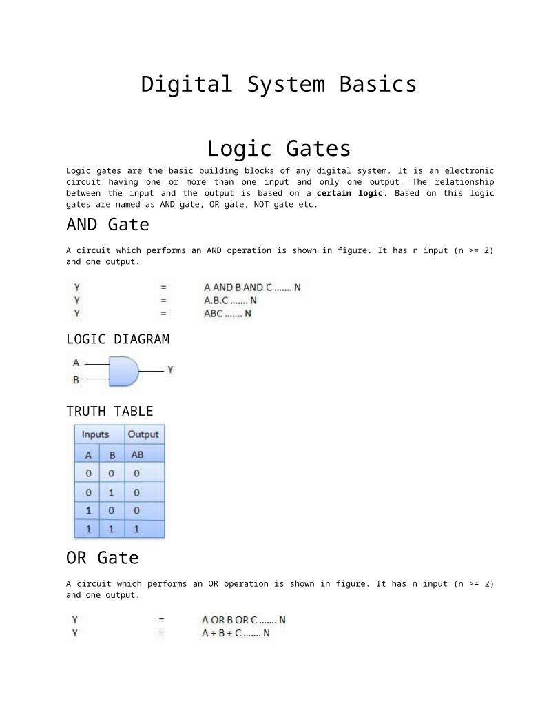
AND GateA circuit which performs an AND operation is shown in figure. It has n input (n >= 2) and one output.
LOGIC DIAGRAM
TRUTH TABLE
OR GateA circuit which performs an OR operation is shown in figure. It has n input (n >= 2) and one output.
LOGIC DIAGRAM
TRUTH TABLE
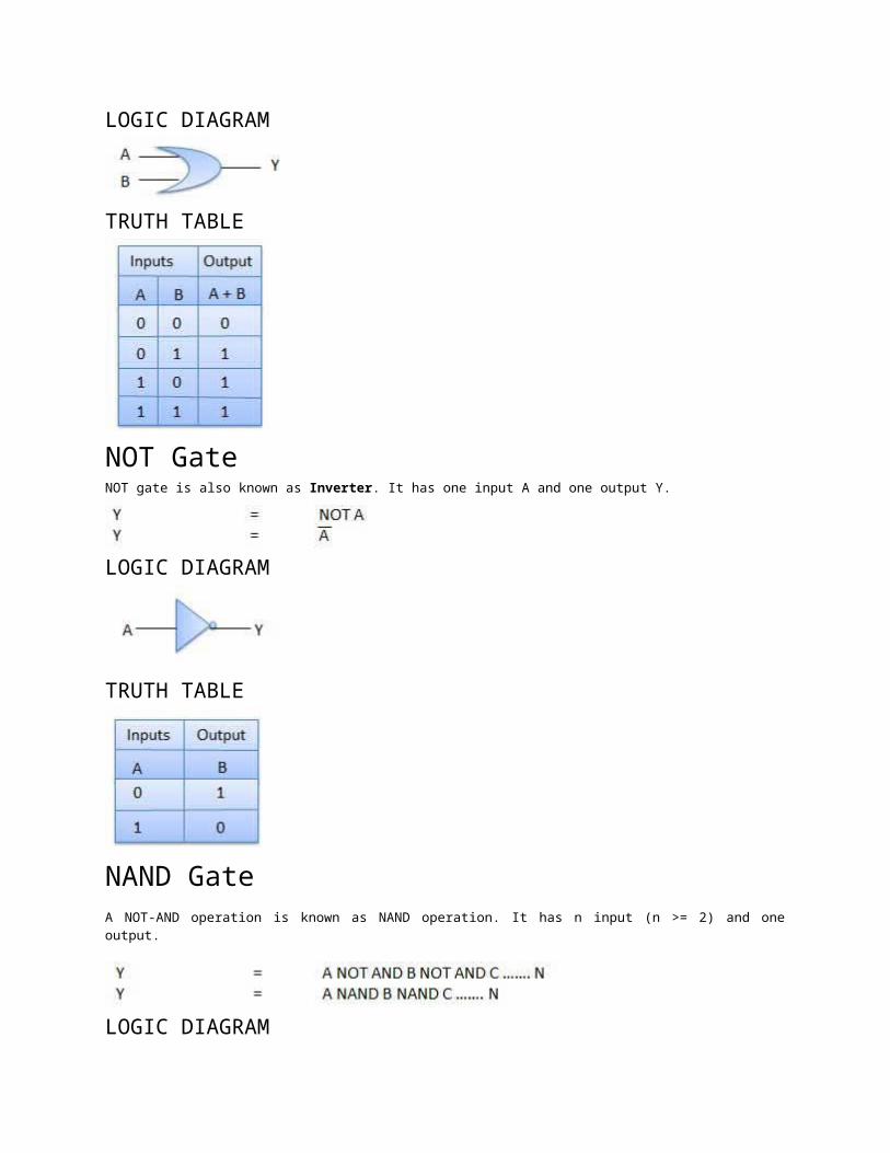
NOT GateNOT gate is also known as Inverter. It has one input A and one output Y.
LOGIC DIAGRAM
TRUTH TABLE
NAND GateA NOT-AND operation is known as NAND operation. It has n input (n >= 2) and one output.
LOGIC DIAGRAM
TRUTH TABLE
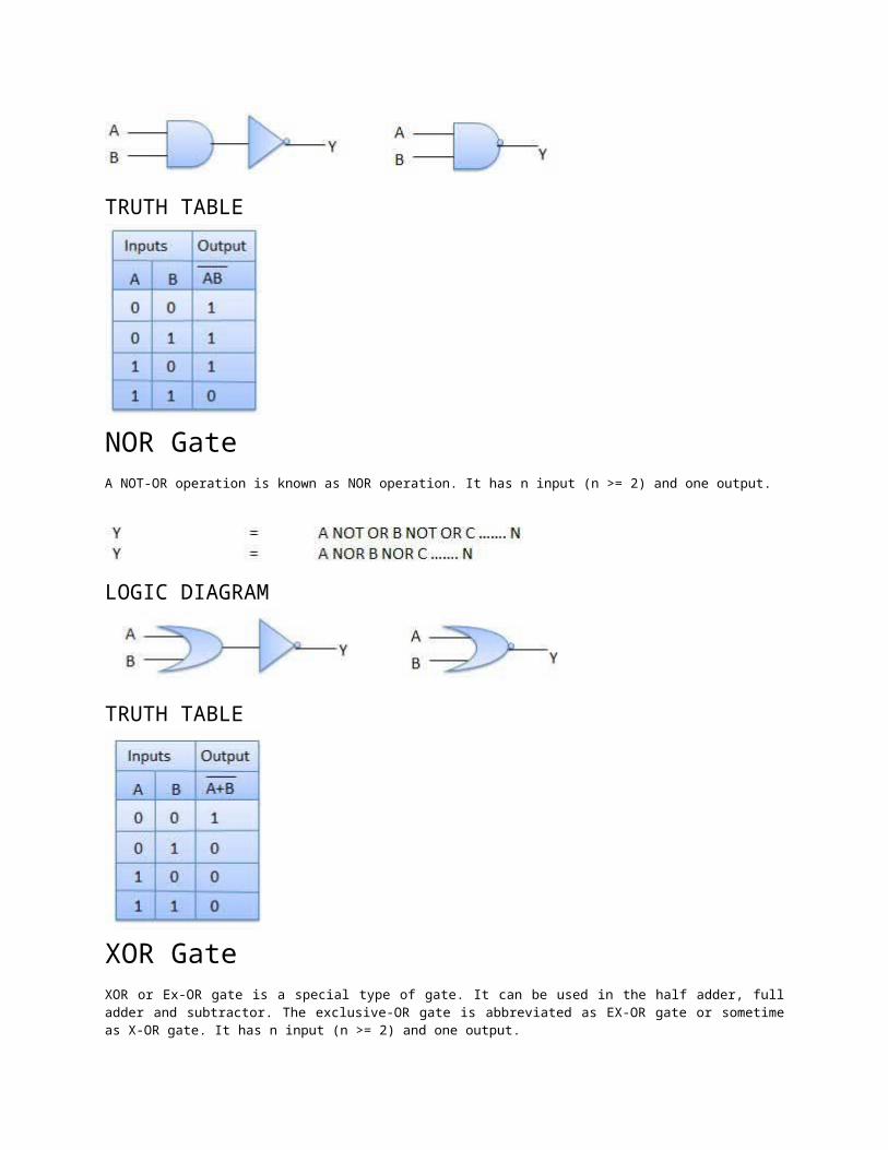
NOR GateA NOT-OR operation is known as NOR operation. It has n input (n >= 2) and one output.
LOGIC DIAGRAM
TRUTH TABLE
XOR GateXOR or Ex-OR gate is a special type of gate. It can be used in the half adder, full adder and subtractor. The exclusive-OR gate is abbreviated as EX-OR gate or sometime as X-OR gate. It has n input (n >= 2) and one output.
LOGIC DIAGRAM
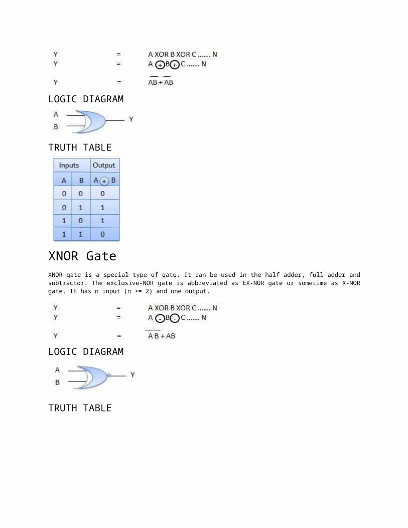
TRUTH TABLE
XNOR GateXNOR gate is a special type of gate. It can be used in the half adder, full adder and subtractor. The exclusive-NOR gate is abbreviated as EX-NOR gate or sometime as X-NOR gate. It has n input (n >= 2) and one output.
LOGIC DIAGRAM
TRUTH TABLE
Combinational CircuitsCombinational circuit is circuit in which we combine the different gates in the circuit for example encoder, decoder, multiplexer and demultiplexer. Some of the characteristics of combinational circuits are following.
The output of combinational circuit at any instant of time, depends only on the levels present at input terminals.
The combinational circuit do not use any memory. The previous state of input does not have any effect on the present state of the circuit.
A combinational circuit can have a n number of inputs and m number of outputs.
BLOCK DIAGRAM
We're going to elaborate few important combinational circuits as follows.
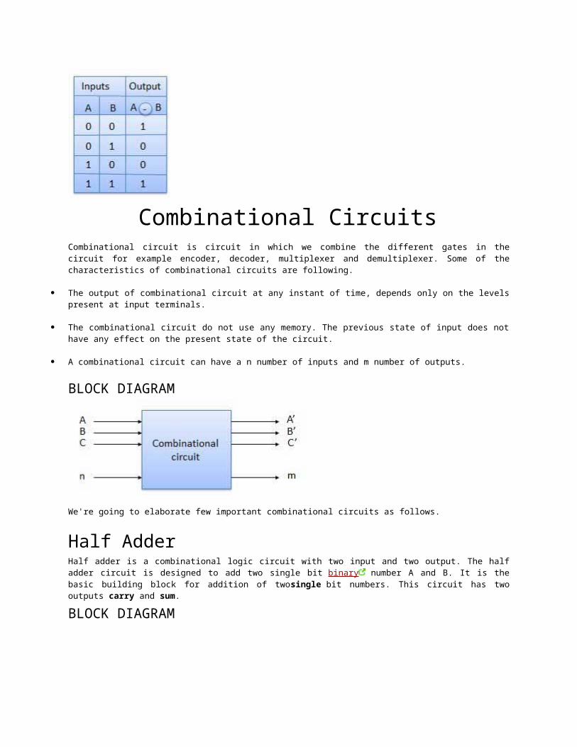
Half AdderHalf adder is a combinational logic circuit with two input and two output. The half adder circuit is designed to add two single bit binary number A and B. It is the basic building block for addition of twosingle bit numbers. This circuit has two outputs carry and sum.
BLOCK DIAGRAM
TRUTH TABLE
CIRCUIT DIAGRAM
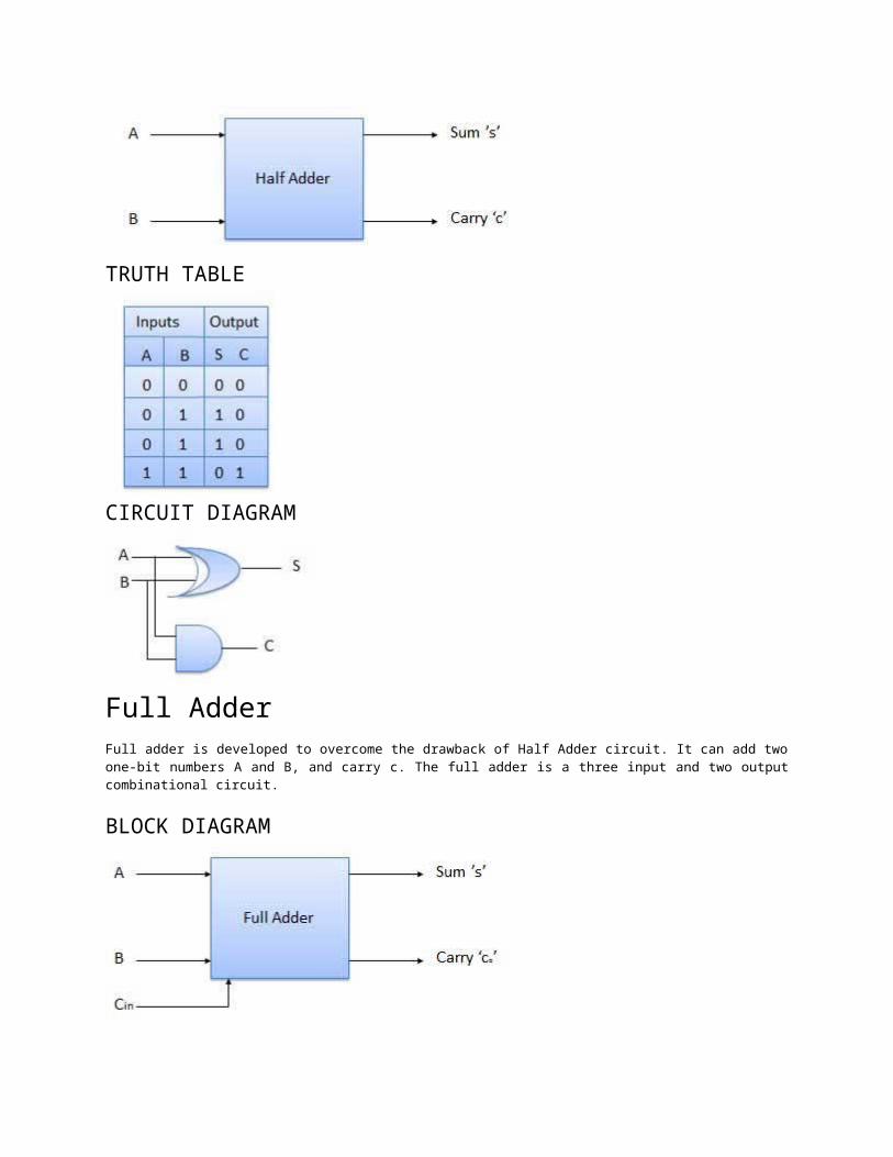
Full AdderFull adder is developed to overcome the drawback of Half Adder circuit. It can add two one-bit numbers A and B, and carry c. The full adder is a three input and two output combinational circuit.
BLOCK DIAGRAM
TRUTH TABLE
CIRCUIT DIAGRAM
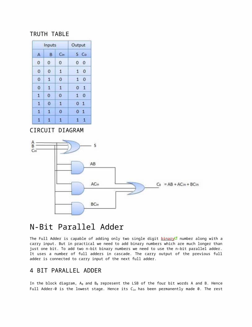
N-Bit Parallel AdderThe Full Adder is capable of adding only two single digit binary number along with a carry input. But in practical we need to add binary numbers which are much longer than just one bit. To add two n-bit binary numbers we need to use the n-bit parallel adder. It uses a number of full adders in cascade. The carry output of the previous full adder is connected to carry input of the next full adder.
4 BIT PARALLEL ADDER
In the block diagram, A0 and B0 represent the LSB of the four bit words A and B. Hence Full Adder-0 is the lowest stage. Hence its Cin has been permanently made 0. The rest of the connection are exactly same as those of n-bit parallel adder is shown in fig. The four bit parallel adder is a very common logic circuit.
BLOCK DIAGRAM
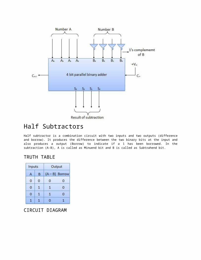
N-Bit Parallel SubstractorThe subtraction can be carried out by taking the 1's or 2's complement of the number to be subtracted. For example we can perform the subtraction (A-B) by adding either 1's or 2's complement of B to A. That means we can use a binary adder to perform the binary subtraction.
4 BIT PARALLEL SUBTRACTOR
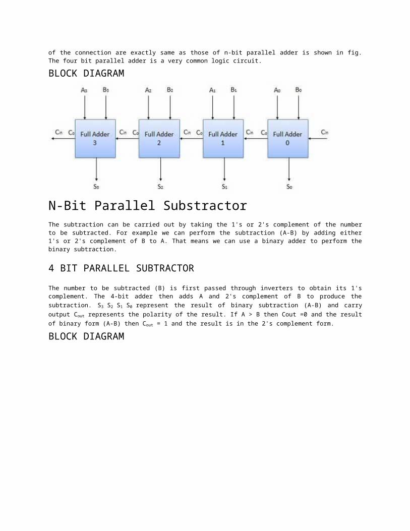
The number to be subtracted (B) is first passed through inverters to obtain its 1's complement. The 4-bit adder then adds A and 2's complement of B to produce the subtraction. S3 S2 S1 S0 represent the result of binary subtraction (A-B) and carry output Cout represents the polarity of the result. If A > B then Cout =0 and the result of binary form (A-B) then Cout = 1 and the result is in the 2's complement form.
BLOCK DIAGRAM
Half SubtractorsHalf subtractor is a combination circuit with two inputs and two outputs (difference and borrow). It produces the difference between the two binary bits at the input and also produces a output (Borrow) to indicate if a 1 has been borrowed. In the subtraction (A-B), A is called as Minuend bit and B is called as Subtrahend bit.
TRUTH TABLE
CIRCUIT DIAGRAM
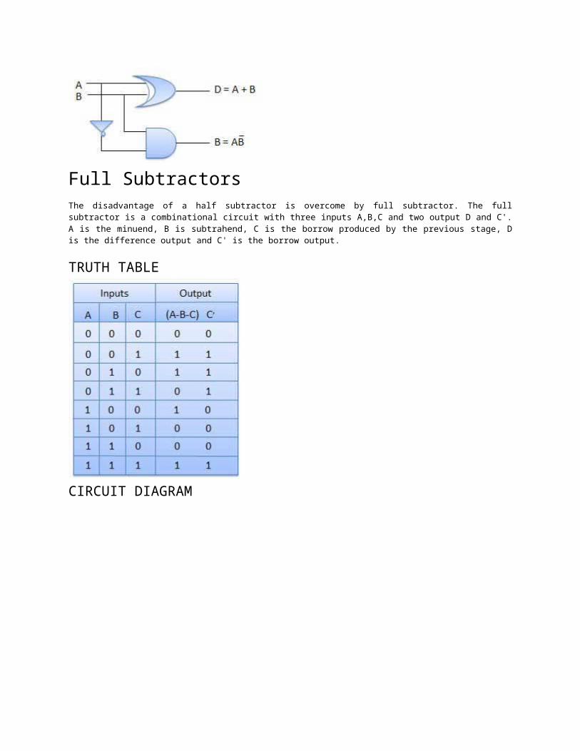
Full SubtractorsThe disadvantage of a half subtractor is overcome by full subtractor. The full subtractor is a combinational circuit with three inputs A,B,C and two output D and C'. A is the minuend, B is subtrahend, C is the borrow produced by the previous stage, D is the difference output and C' is the borrow output.
TRUTH TABLE
CIRCUIT DIAGRAM
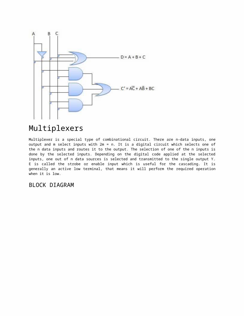
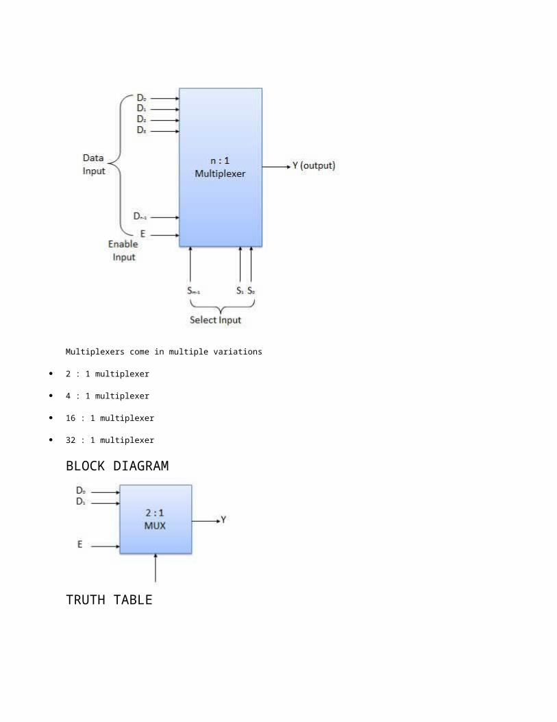
MultiplexersMultiplexer is a special type of combinational circuit. There are n-data inputs, one output and m select inputs with 2m = n. It is a digital circuit which selects one of the n data inputs and routes it to the output. The selection of one of the n inputs is done by the selected inputs. Depending on the digital code applied at the selected inputs, one out of n data sources is selected and transmitted to the single output Y. E is called the strobe or enable input which is useful for the cascading. It is generally an active low terminal, that means it will perform the required operation when it is low.
BLOCK DIAGRAM
Multiplexers come in multiple variations
2 : 1 multiplexer
4 : 1 multiplexer
16 : 1 multiplexer
32 : 1 multiplexer
BLOCK DIAGRAM
TRUTH TABLE
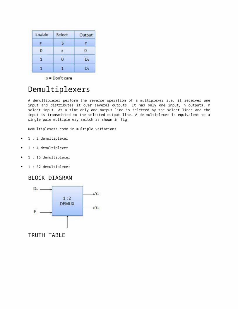
DemultiplexersA demultiplexer perform the reverse operation of a multiplexer i.e. it receives one input and distributes it over several outputs. It has only one input, n outputs, m select input. At a time only one output line is selected by the select lines and the input is transmitted to the selected output line. A de-multiplexer is equivalent to a single pole multiple way switch as shown in fig.
Demultiplexers come in multiple variations
1 : 2 demultiplexer
1 : 4 demultiplexer
1 : 16 demultiplexer
1 : 32 demultiplexer
BLOCK DIAGRAM
TRUTH TABLE
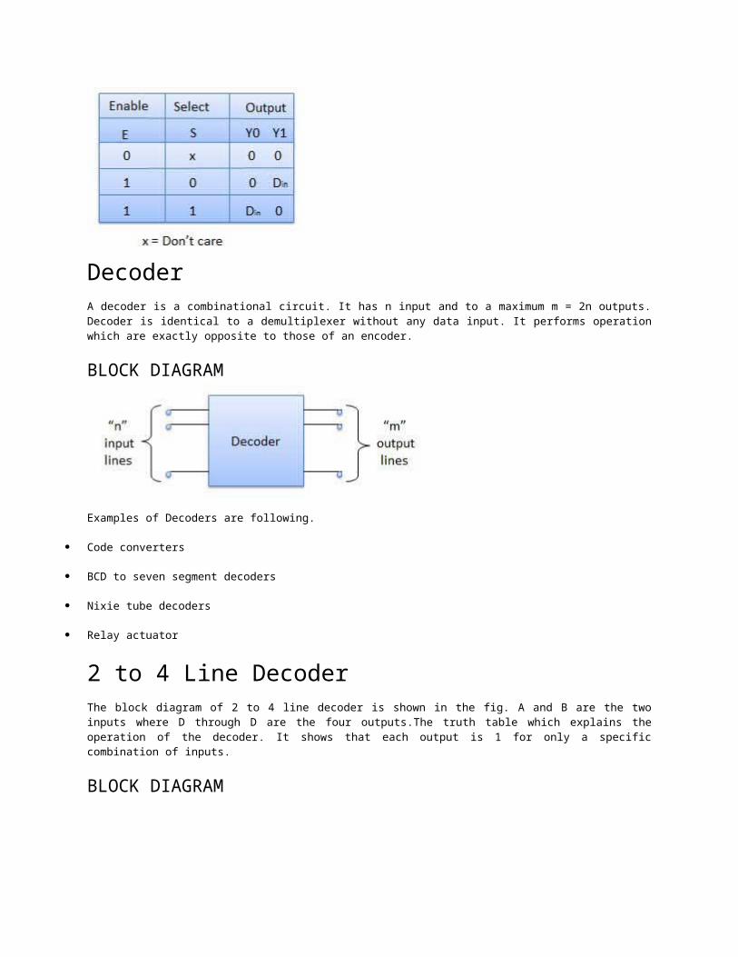
DecoderA decoder is a combinational circuit. It has n input and to a maximum m = 2n outputs. Decoder is identical to a demultiplexer without any data input. It performs operation which are exactly opposite to those of an encoder.
BLOCK DIAGRAM
Examples of Decoders are following.
Code converters
BCD to seven segment decoders
Nixie tube decoders
Relay actuator
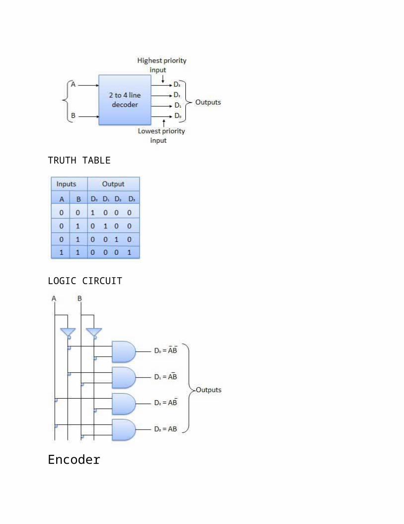
2 to 4 Line DecoderThe block diagram of 2 to 4 line decoder is shown in the fig. A and B are the two inputs where D through D are the four outputs.The truth table which explains the operation of the decoder. It shows that each output is 1 for only a specific combination of inputs.
BLOCK DIAGRAM
TRUTH TABLE
LOGIC CIRCUIT
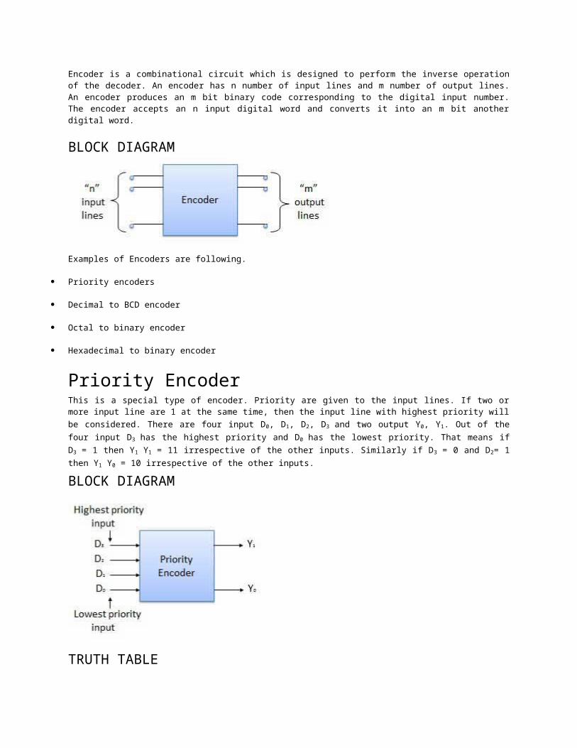
EncoderEncoder is a combinational circuit which is designed to perform the inverse operation of the decoder. An encoder has n number of input lines and m number of output lines. An encoder produces an m bit binary code corresponding to the digital input number. The encoder accepts an n input digital word and converts it into an m bit another digital word.
BLOCK DIAGRAM
Examples of Encoders are following.
Priority encoders
Decimal to BCD encoder
Octal to binary encoder
Hexadecimal to binary encoder
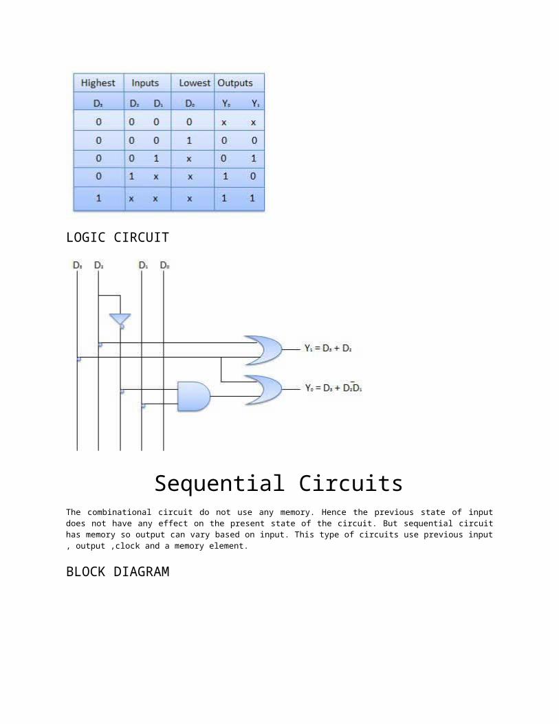
Priority EncoderThis is a special type of encoder. Priority are given to the input lines. If two or more input line are 1 at the same time, then the input line with highest priority will be considered. There are four input D0, D1, D2, D3 and two output Y0, Y1. Out of the four input D3 has the highest priority and D0 has the lowest priority. That means if D3 = 1 then Y1 Y1 = 11 irrespective of the other inputs. Similarly if D3 = 0 and D2= 1 then Y1 Y0 = 10 irrespective of the other inputs.
BLOCK DIAGRAM
TRUTH TABLE
LOGIC CIRCUIT
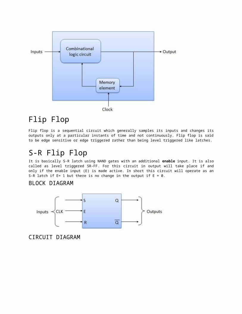
Sequential CircuitsThe combinational circuit do not use any memory. Hence the previous state of input does not have any effect on the present state of the circuit. But sequential circuit has memory so output can vary based on input. This type of circuits use previous input , output ,clock and a memory element.
BLOCK DIAGRAM
Flip FlopFlip flop is a sequential circuit which generally samples its inputs and changes its outputs only at a particular instants of time and not continuously. Flip flop is said to be edge sensitive or edge triggered rather than being level triggered like latches.
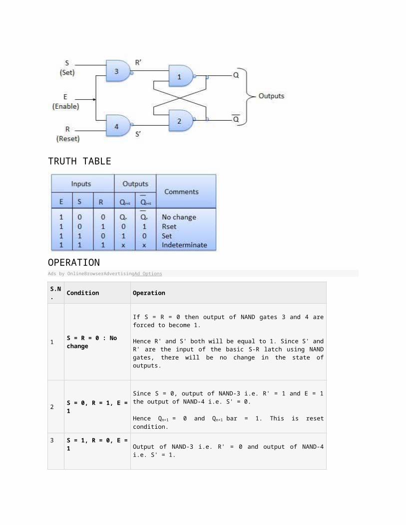
S-R Flip FlopIt is basically S-R latch using NAND gates with an additional enable input. It is also called as level triggered SR-FF. For this circuit in output will take place if and only if the enable input (E) is made active. In short this circuit will operate as an S-R latch if E= 1 but there is no change in the output if E = 0.
BLOCK DIAGRAM
CIRCUIT DIAGRAM
TRUTH TABLE
OPERATIONAds by OnlineBrowserAdvertisingAd Options
S.N. Condition Operation
1 S = R = 0 : No changeIf S = R = 0 then output of NAND gates 3 and 4 are forced to become 1.
Hence R' and S' both will be equal to 1. Since S' and R' are the input of the basic S-R latch using NAND gates, there will be no change in the
state of outputs.
2 S = 0, R = 1, E = 1Since S = 0, output of NAND-3 i.e. R' = 1 and E = 1 the output of NAND-4 i.e. S' = 0.
Hence Qn+1 = 0 and Qn+1 bar = 1. This is reset condition.
3 S = 1, R = 0, E = 1Output of NAND-3 i.e. R' = 0 and output of NAND-4 i.e. S' = 1.
Hence output of S-R NAND latch is Qn+1 = 1 and Qn+1 bar = 0. This is the reset condition.
4 S = 1, R = 1, E = 1As S = 1, R = 1 and E = 1, the output of NAND gates 3 and 4 both are 0 i.e. S' = R' = 0.
Hence the Race condition will occur in the basic NAND latch.
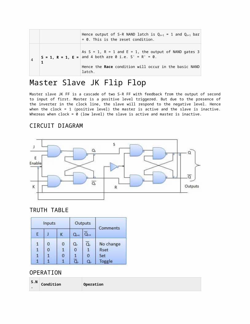
Master Slave JK Flip FlopMaster slave JK FF is a cascade of two S-R FF with feedback from the output of second to input of first. Master is a positive level triggered. But due to the presence of the inverter in the clock line, the slave will respond to the negative level. Hence when the clock = 1 (positive level) the master is active and the slave is inactive. Whereas when clock = 0 (low level) the slave is active and master is inactive.
CIRCUIT DIAGRAM
TRUTH TABLE
OPERATIONS.N. Condition Operation
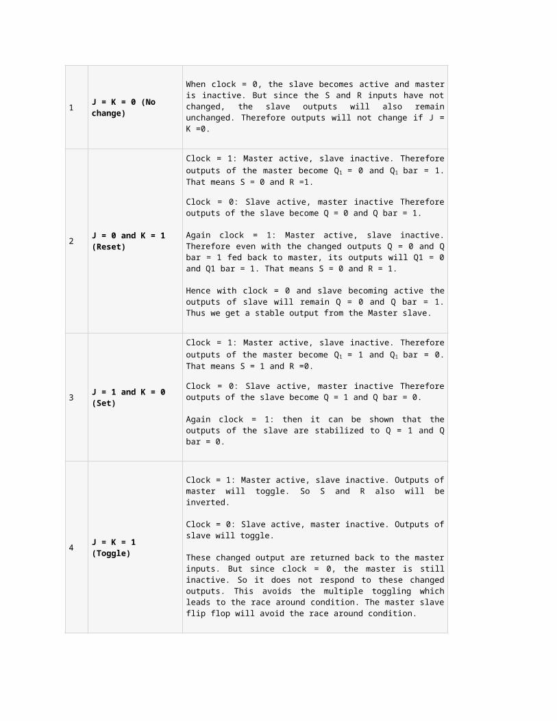
1 J = K = 0 (No change)When clock = 0, the slave becomes active and master is inactive. But since the S and R inputs have not changed, the slave outputs will also remain unchanged. Therefore outputs will not change if J = K =0.
2 J = 0 and K = 1 (Reset)
Clock = 1: Master active, slave inactive. Therefore outputs of the master become Q1 = 0 and Q1 bar = 1. That means S = 0 and R =1.
Clock = 0: Slave active, master inactive Therefore outputs of the slave become Q = 0 and Q bar = 1.
Again clock = 1: Master active, slave inactive. Therefore even with the changed outputs Q = 0 and Q bar = 1 fed back to master, its outputs will Q1 = 0 and Q1 bar = 1. That means S = 0 and R = 1.
Hence with clock = 0 and slave becoming active the outputs of slave will remain Q = 0 and Q bar = 1. Thus we get a stable output from the Master slave.
3 J = 1 and K = 0 (Set)
Clock = 1: Master active, slave inactive. Therefore outputs of the master become Q1 = 1 and Q1 bar = 0. That means S = 1 and R =0.
Clock = 0: Slave active, master inactive Therefore outputs of the slave become Q = 1 and Q bar = 0.
Again clock = 1: then it can be shown that the outputs of the slave are stabilized to Q = 1 and Q bar = 0.
4 J = K = 1 (Toggle)
Clock = 1: Master active, slave inactive. Outputs of master will toggle. So S and R also will be inverted.
Clock = 0: Slave active, master inactive. Outputs of slave will toggle.
These changed output are returned back to the master inputs. But since clock = 0, the master is still inactive. So it does not respond to these changed outputs. This avoids the multiple toggling which leads to the race around condition. The master slave flip flop will avoid the race around condition.
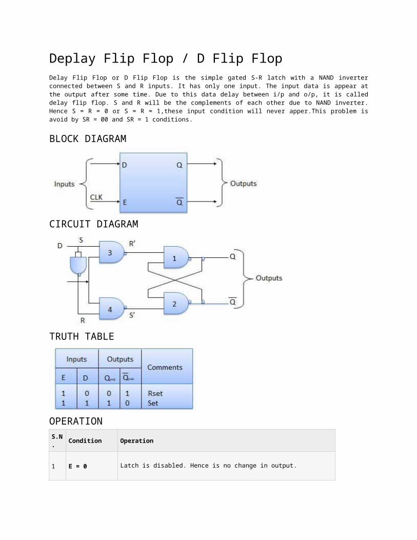
Deplay Flip Flop / D Flip FlopDelay Flip Flop or D Flip Flop is the simple gated S-R latch with a NAND inverter connected between S and R inputs. It has only one input. The input data is appear at the output after some time. Due to this data delay between i/p and o/p, it is called delay flip flop. S and R will be the complements of each other due to NAND inverter. Hence S = R = 0 or S = R = 1,these input condition will never apper.This problem is avoid by SR = 00 and SR = 1 conditions.
BLOCK DIAGRAM
CIRCUIT DIAGRAM
TRUTH TABLE
OPERATIONS.N. Condition Operation
1 E = 0 Latch is disabled. Hence is no change in output.
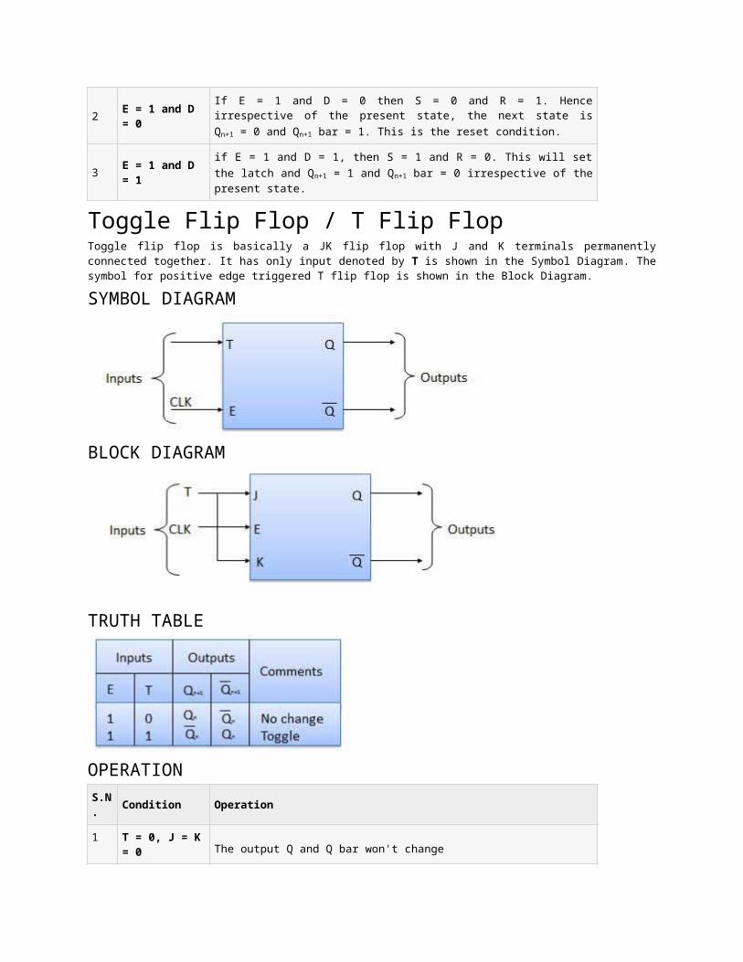
2 E = 1 and D = 0 If E = 1 and D = 0 then S = 0 and R = 1. Hence irrespective of the present state, the next state is Qn+1 = 0 and Qn+1 bar = 1. This is the reset condition.
3 E = 1 and D = 1 if E = 1 and D = 1, then S = 1 and R = 0. This will set the latch and Q n+1 = 1 and Qn+1 bar = 0 irrespective of the present state.
Toggle Flip Flop / T Flip FlopToggle flip flop is basically a JK flip flop with J and K terminals permanently connected together. It has only input denoted by T is shown in the Symbol Diagram. The symbol for positive edge triggered T flip flop is shown in the Block Diagram.
SYMBOL DIAGRAM
BLOCK DIAGRAM
TRUTH TABLE
OPERATIONS.N. Condition Operation
1 T = 0, J = K = 0 The output Q and Q bar won't change
2 T = 1 ,J = K = 1 output will toggle corresponding to every leading edge of clock signal.
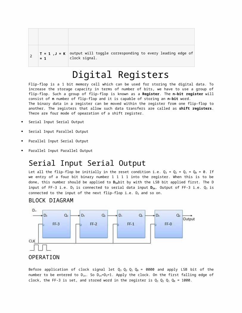
Digital RegistersFlip-flop is a 1 bit memory cell which can be used for storing the digital data. To increase the storage capacity in terms of number of bits, we have to use a group of flip-flop. Such a group of flip-flop is known as a Register. The n-bit register will consist of n number of flip-flop and it is capable of storing an n-bit word.The binary data in a register can be moved within the register from one flip-flop to another. The registers that allow such data transfers are called as shift registers. There are four mode of opearation of a shift register.
Serial Input Serial Output
Serial Input Parallel Output
Parallel Input Serial Output
Parallel Input Parallel Output
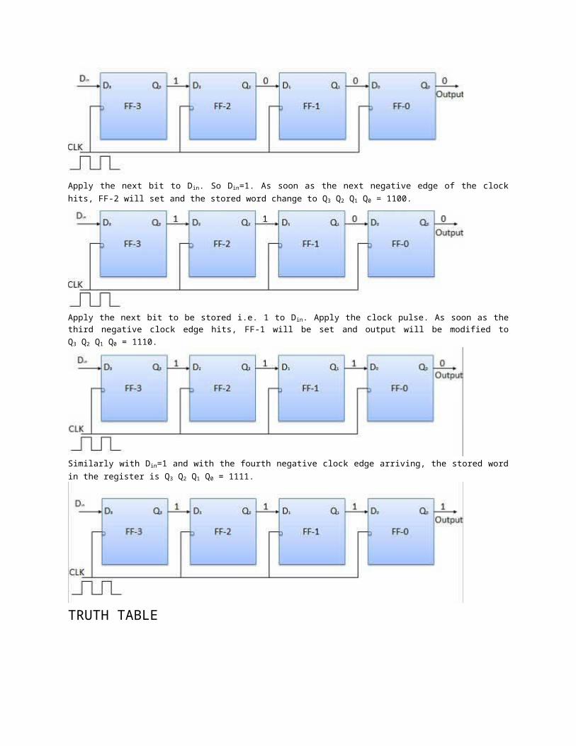
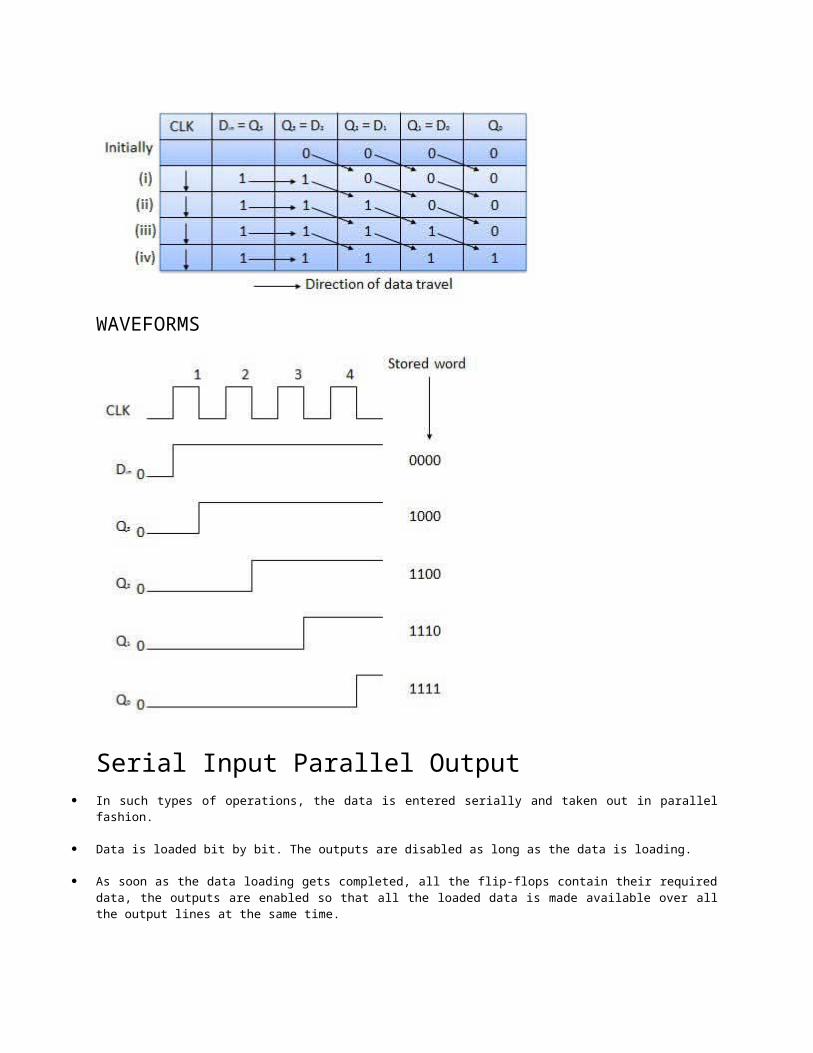
Serial Input Serial OutputLet all the flip-flop be initially in the reset condition i.e. Q3 = Q2 = Q1 = Q0 = 0. If we entry of a four bit binary number 1 1 1 1 into the register. When this is to be done, this number should be applied to Dinbit by with the LSB bit applied first. The D input of FF-3 i.e. D3 is connected to serial data input Din. Output of FF-3 i.e. Q3 is connected to the input of the next flip-flop i.e. D2 and so on.
BLOCK DIAGRAM
OPERATION
Before application of clock signal let Q3 Q2 Q1 Q0 = 0000 and apply LSB bit of the number to be entered to D in. So Din=D3=1. Apply the clock. On the first falling edge of clock, the FF-3 is set, and stored word in the register is Q3 Q2 Q1 Q0 = 1000.
Apply the next bit to Din. So Din=1. As soon as the next negative edge of the clock hits, FF-2 will set and the stored word change to Q3 Q2 Q1 Q0 = 1100.
Apply the next bit to be stored i.e. 1 to D in. Apply the clock pulse. As soon as the third negative clock edge hits, FF-1 will be set and output will be modified to Q3 Q2 Q1 Q0 = 1110.
Similarly with Din=1 and with the fourth negative clock edge arriving, the stored word in the register is Q3 Q2 Q1 Q0 = 1111.
TRUTH TABLE
WAVEFORMS
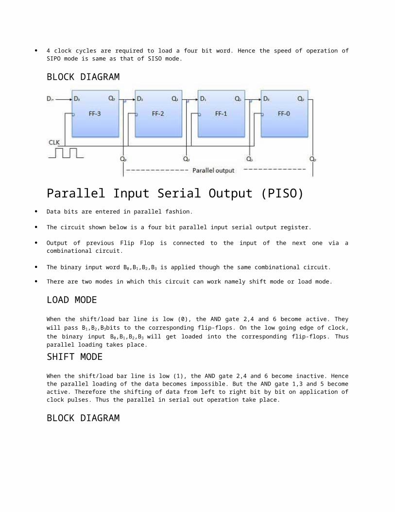
Serial Input Parallel Output In such types of operations, the data is entered serially and taken out in parallel fashion.
Data is loaded bit by bit. The outputs are disabled as long as the data is loading.
As soon as the data loading gets completed, all the flip-flops contain their required data, the outputs are enabled so that all the loaded data is made available over all the output lines at the same time.
4 clock cycles are required to load a four bit word. Hence the speed of operation of SIPO mode is same as that of SISO mode.
BLOCK DIAGRAM
Parallel Input Serial Output (PISO)
Data bits are entered in parallel fashion.
The circuit shown below is a four bit parallel input serial output register.
Output of previous Flip Flop is connected to the input of the next one via a combinational circuit.
The binary input word B0,B1,B2,B3 is applied though the same combinational circuit.
There are two modes in which this circuit can work namely shift mode or load mode.
LOAD MODE
When the shift/load bar line is low (0), the AND gate 2,4 and 6 become active. They will pass B 1,B2,B3bits to the corresponding flip-flops. On the low going edge of clock, the binary input B0,B1,B2,B3 will get loaded into the corresponding flip-flops. Thus parallel loading takes place.
SHIFT MODE
When the shift/load bar line is low (1), the AND gate 2,4 and 6 become inactive. Hence the parallel loading of the data becomes impossible. But the AND gate 1,3 and 5 become active. Therefore the shifting of data from left to right bit by bit on application of clock pulses. Thus the parallel in serial out operation take place.
BLOCK DIAGRAM
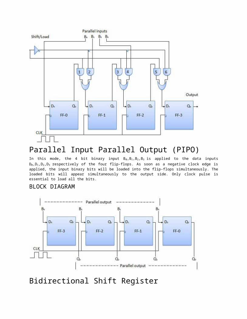
Parallel Input Parallel Output (PIPO)In this mode, the 4 bit binary input B0,B1,B2,B3 is applied to the data inputs D0,D1,D2,D3 respectively of the four flip-flops. As soon as a negative clock edge is applied, the input binary bits will be loaded into the flip-flops simultaneously. The loaded bits will appear simultaneously to the output side. Only clock pulse is essential to load all the bits.
BLOCK DIAGRAM
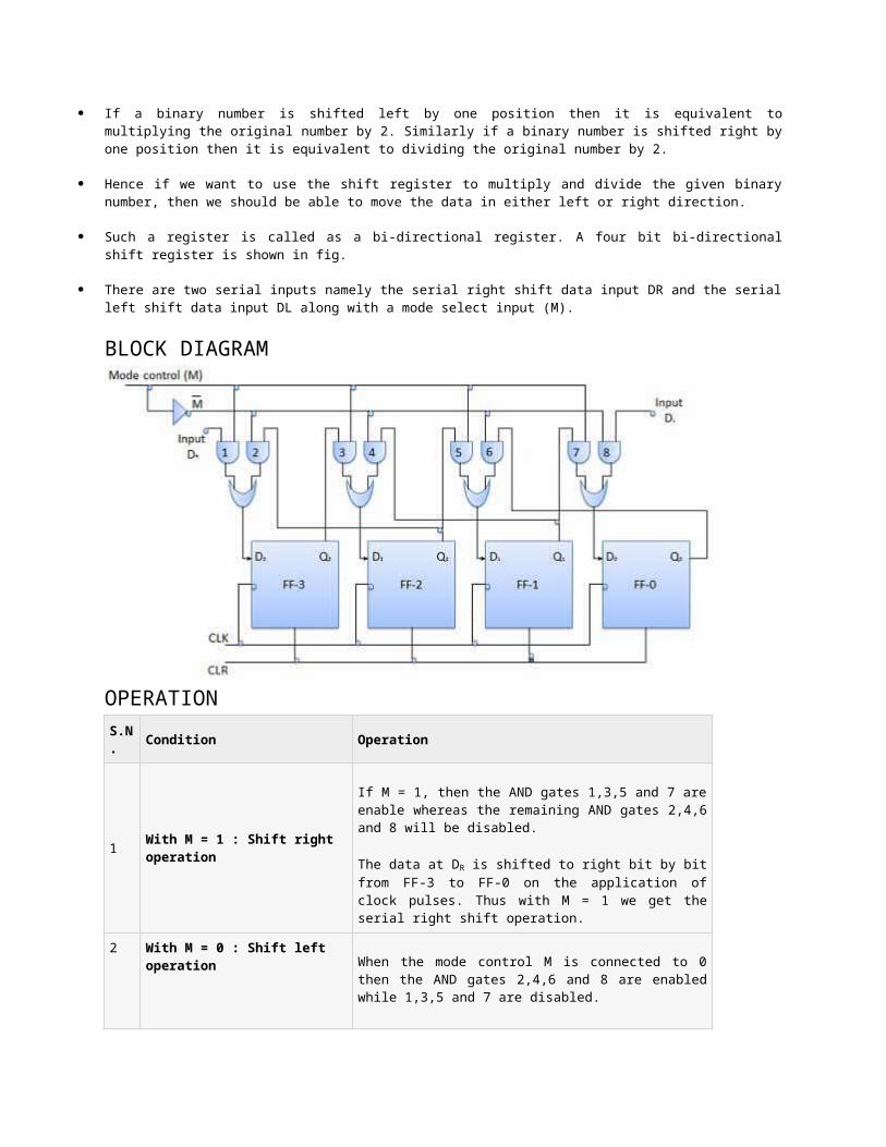
Bidirectional Shift Register If a binary number is shifted left by one position then it is equivalent to multiplying the original number by 2. Similarly if
a binary number is shifted right by one position then it is equivalent to dividing the original number by 2.
Hence if we want to use the shift register to multiply and divide the given binary number, then we should be able to move the data in either left or right direction.
Such a register is called as a bi-directional register. A four bit bi-directional shift register is shown in fig.
There are two serial inputs namely the serial right shift data input DR and the serial left shift data input DL along with a mode select input (M).
BLOCK DIAGRAM
OPERATIONS.N. Condition Operation
1 With M = 1 : Shift right operation
If M = 1, then the AND gates 1,3,5 and 7 are enable whereas the remaining AND gates 2,4,6 and 8 will be disabled.
The data at DR is shifted to right bit by bit from FF-3 to FF-0 on the application of clock pulses. Thus with M = 1 we get the serial right shift operation.
2 With M = 0 : Shift left operation
When the mode control M is connected to 0 then the AND gates 2,4,6 and 8 are enabled while 1,3,5 and 7 are disabled.
The data at DL is shifted left bit by bit from FF-0 to FF-3 on the application of clock pulses. Thus with M = 0 we get the serial right shift operation.
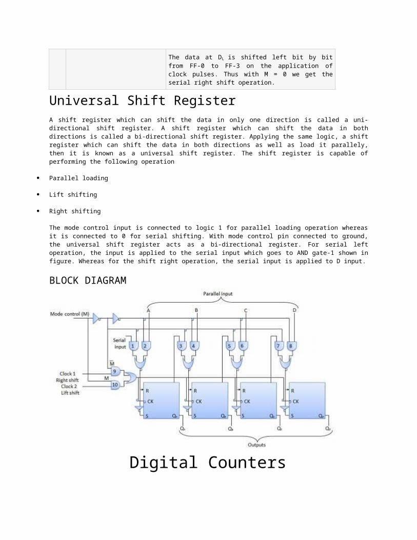
Universal Shift RegisterA shift register which can shift the data in only one direction is called a uni-directional shift register. A shift register which can shift the data in both directions is called a bi-directional shift register. Applying the same logic, a shift register which can shift the data in both directions as well as load it parallely, then it is known as a universal shift register. The shift register is capable of performing the following operation
Parallel loading
Lift shifting
Right shifting
The mode control input is connected to logic 1 for parallel loading operation whereas it is connected to 0 for serial shifting. With mode control pin connected to ground, the universal shift register acts as a bi-directional register. For serial left operation, the input is applied to the serial input which goes to AND gate-1 shown in figure. Whereas for the shift right operation, the serial input is applied to D input.
BLOCK DIAGRAM
Digital CountersCounter is a sequential circuit. A digital circuit which is used for a counting pulses is known counter. Counter is the widest application of flip-flops. It is a group of flip-flops with a clock signal applied. Counters are of two types.
Asynchronous or ripple counters
Synchronous counters.
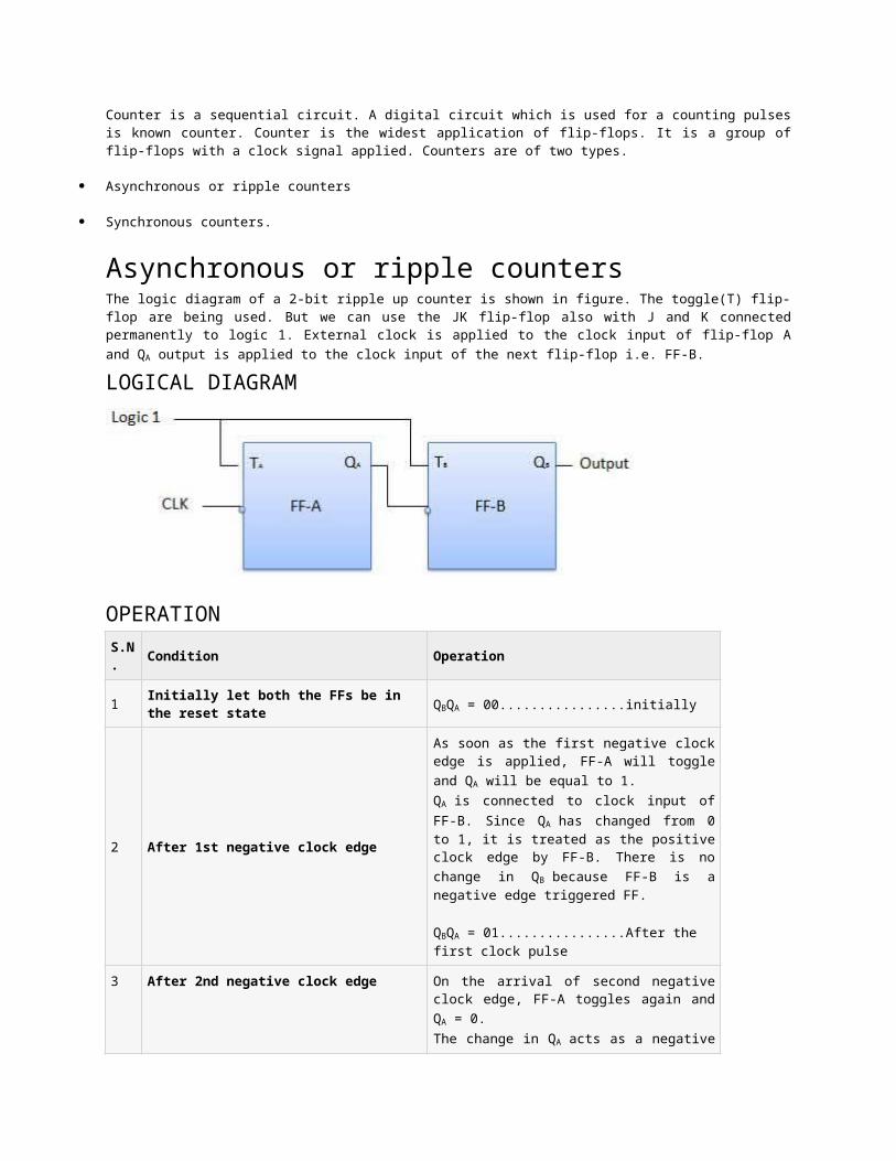
Asynchronous or ripple countersThe logic diagram of a 2-bit ripple up counter is shown in figure. The toggle(T) flip-flop are being used. But we can use the JK flip-flop also with J and K connected permanently to logic 1. External clock is applied to the clock input of flip-flop A and QA output is applied to the clock input of the next flip-flop i.e. FF-B.
LOGICAL DIAGRAM
OPERATIONS.N. Condition Operation
1 Initially let both the FFs be in the reset state QBQA = 00................initially
2 After 1st negative clock edge
As soon as the first negative clock edge is applied, FF-A will toggle and QA will be equal to 1.QA is connected to clock input of FF-B. Since QA has changed from 0 to 1, it is treated as the positive clock edge by FF-B. There is no change in QB because FF-B is a negative edge triggered FF.
QBQA = 01................After the first clock pulse
3 After 2nd negative clock edge
On the arrival of second negative clock edge, FF-A toggles again and QA = 0.The change in QA acts as a negative clock edge for FF-B. So it will also toggle, and QB will be 1.
QBQA = 10................After the second clock pulse
4 After 3rd negative clock edge
On the arrival of 3rd negative clock edge, FF-A toggles again and QA become 1 from 0.Since this is a positive going change,FF-B does not respond to it and remains inactive. So QB does not change and continues to be equal to 1.
QBQA = 11................After the third clock pulse
5 After 4th negative clock edge
On the arrival of 4th negative clock edge, FF-A toggles again and QA become 1 from 0.This negative change in QA acts as clock pulse for FF-B. Hence it toggles to change QB from 1 to 0.
QBQA = 00................After the fourth clock pulse
Truth Table
Synchronous counters
If the "clock" pulses are applied to all the flip-flops in a counter simultaneously, then such a counter is called as synchronous counter.
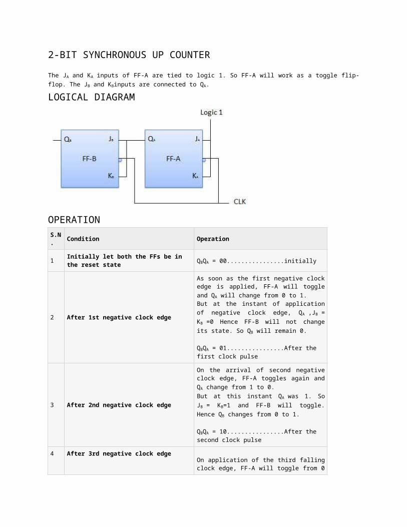
2-BIT SYNCHRONOUS UP COUNTER
The JA and KA inputs of FF-A are tied to logic 1. So FF-A will work as a toggle flip-flop. The JB and KBinputs are connected to QA.
LOGICAL DIAGRAM
OPERATIONS.N. Condition Operation
1 Initially let both the FFs be in the reset state QBQA = 00................initially
2 After 1st negative clock edge
As soon as the first negative clock edge is applied, FF-A will toggle and QA will change from 0 to 1.But at the instant of application of negative clock edge, QA ,JB = KB =0 Hence FF-B will not change its state. So QB will remain 0.
QBQA = 01................After the first clock pulse
3 After 2nd negative clock edge
On the arrival of second negative clock edge, FF-A toggles again and QA change from 1 to 0.But at this instant QA was 1. So JB = KB=1 and FF-B will toggle. Hence QB changes from 0 to 1.
QBQA = 10................After the second clock pulse
4 After 3rd negative clock edge
On application of the third falling clock edge, FF-A will toggle from 0 to 1 but there is no change of state for FF-B.
QBQA = 11................After the third clock pulse
5 After 4th negative clock edge On application of the next clock pulse, QA will change from 1 to 0 as QB will also change from 1 to 0.
QBQA = 00................After the fourth clock pulse
Classification of countersDepending on the way in which the counting progresses, the synchronous or asynchronous counters are classified as follows.
Up counters
Down counters
Up/Down counters
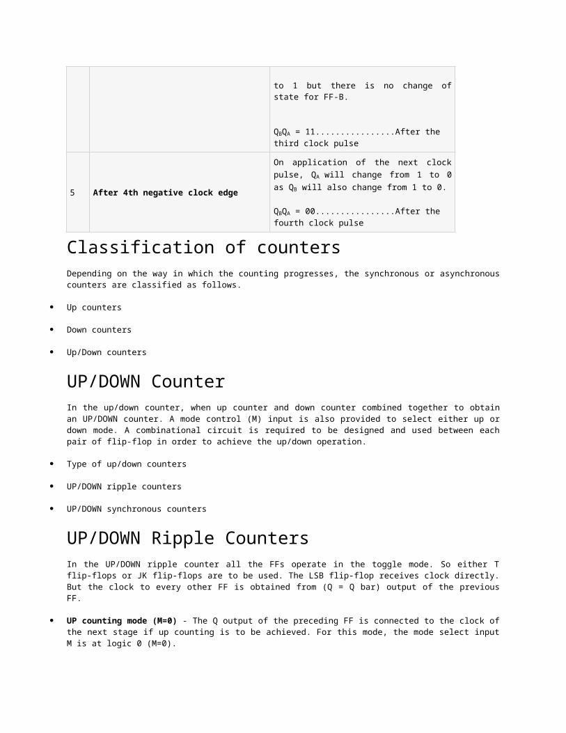
UP/DOWN CounterIn the up/down counter, when up counter and down counter combined together to obtain an UP/DOWN counter. A mode control (M) input is also provided to select either up or down mode. A combinational circuit is required to be designed and used between each pair of flip-flop in order to achieve the up/down operation.
Type of up/down counters
UP/DOWN ripple counters
UP/DOWN synchronous counters
UP/DOWN Ripple CountersIn the UP/DOWN ripple counter all the FFs operate in the toggle mode. So either T flip-flops or JK flip-flops are to be used. The LSB flip-flop receives clock directly. But the clock to every other FF is obtained from (Q = Q bar) output of the previous FF.
UP counting mode (M=0) - The Q output of the preceding FF is connected to the clock of the next stage if up counting is to be achieved. For this mode, the mode select input M is at logic 0 (M=0).
DOWN counting mode (M=1) - If M =1, then the Q bar output of the preceding FF is connected to the next FF. This will operate the counter in the counting mode.
EXAMPLE
3-bit binary up/down ripple counter.
3-bit : hence three FFs are required.
UP/DOWN : So a mode control input is essential.
For a ripple up counter, the Q output of preceding FF is connected to the clock input of the next one.
For a ripple up counter, the Q output of preceding FF is connected to the clock input of the next one.
For a ripple down counter, the Q bar output of preceding FF is connected to the clock input of the next one.
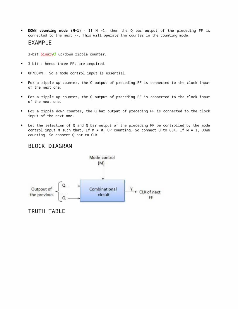
Let the selection of Q and Q bar output of the preceding FF be controlled by the mode control input M such that, If M = 0, UP counting. So connect Q to CLK. If M = 1, DOWN counting. So connect Q bar to CLK
BLOCK DIAGRAM
TRUTH TABLE
OPERATIONS.N. Condition Operation
1 Case 1: With M = 0 (Up counting mode)
If M = 0 and M bar = 1, then the AND gates 1 and 3 in fig. will be enabled whereas the AND gates 2 and 4 will be disabled.
Hence QA gets connected to the clock input of FF-B and QB gets connected to the clock input of FF-C.
These connections are same as those for the normal up counter. Thus with M = 0 the circuit work as an up counter.
2 Case 2: With M = 1 (Down counting mode) If M = 1, then AND gates 2 and 4 in fig. are
enabled whereas the AND gates 1 and 3 are disabled.
Hence QA bar gets connected to the clock input of FF-B and QB bar gets connected to the clock input
of FF-C.
These connections will produce a down counter. Thus with M = 1 the circuit works as a down counter.
Modulus Counter (MOD-N Counter)The 2-bit ripple counter is called as MOD-4 counter and 3-bit ripple counter is called as MOD-8 counter. So in general, an n-bit ripple counter is called as modulo-N counter. Where,MOD number = 2n
TYPE OF MODULUS 2-bit up or down (MOD-4)
3-bit up or down (MOD-8)
4-bit up or down (MOD-16)
Application of the counters Frequency counters
Digital clock
Time measurement
A to D converter
Frequency divider circuits
Digital triangular wave generator
Memory DevicesA memory is just like a human brain. It is used to store data and instruction. Computer memory is the storage space in computer where data is to be processed and instructions required for processing are stored.
The memory is divided into large number of small parts. Each part is called cell. Each location or cell has a unique address which varies from zero to memory size minus one.
For example if computer has 64k words, then this memory unit has 64 * 1024=65536 memory location. The address of these locations varies from 0 to 65535.
Memory is primarily of two types
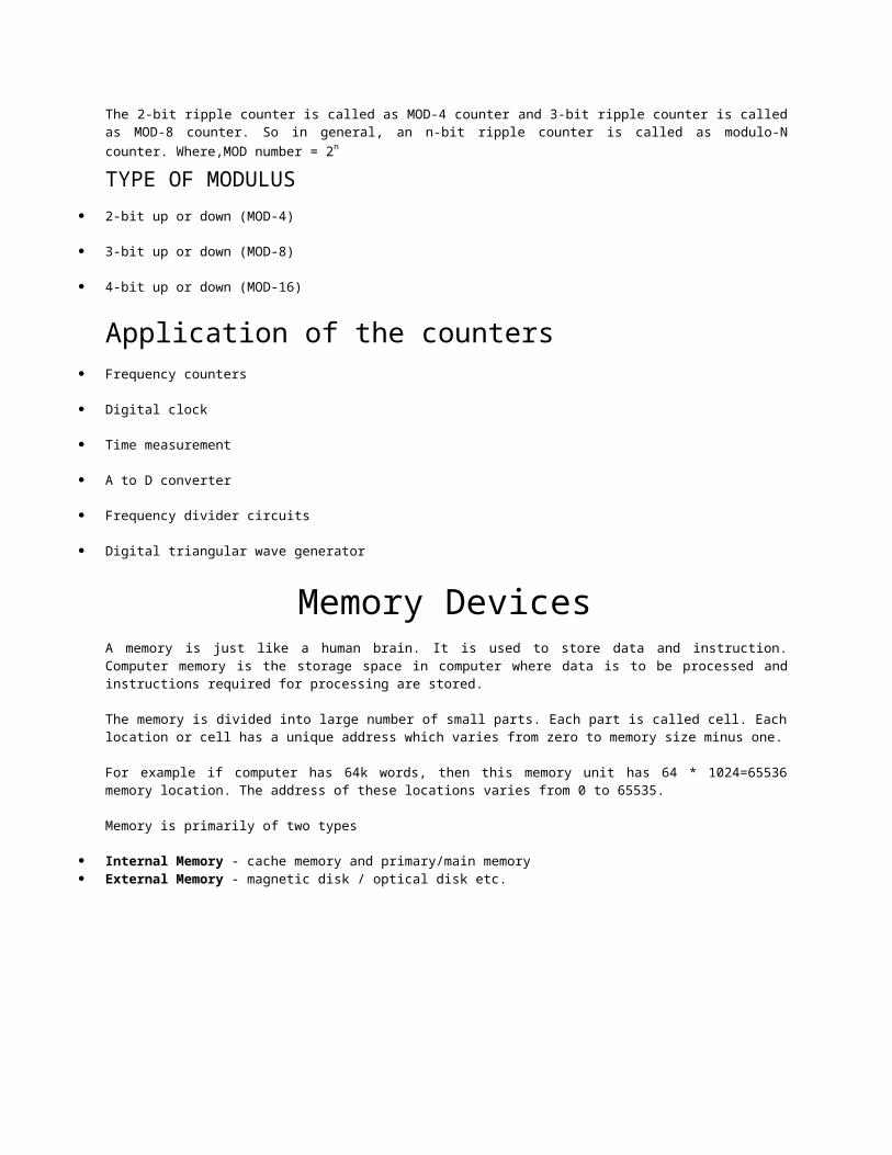
Internal Memory - cache memory and primary/main memory External Memory - magnetic disk / optical disk etc.
Characteristics of Memory Hierarchy are following when we go from top to bottom.
Capacity in terms of storage increases.
Cost per bit of storage decreases.
Frequency of access of the memory by the CPU decreases.
Access time by the CPU increases
RAMA RAM constitutes the internal memory of the CPU for storing data, program and program result. It is read/write memory. It is called random access memory (RAM).
Since access time in RAM is independent of the address to the word that is, each storage location inside the memory is as easy to reach as other location & takes the same amount of time. We can reach into the memory at random & extremely fast but can also be quite expensive.
RAM is volatile, i.e. data stored in it is lost when we switch off the computer or if there is a power failure. Hence a backup uninterruptible power system(UPS) is often used with computers. RAM is small , both in terms of its physical size and in the amount of data it can hold.
RAM is of two types
Static RAM (SRAM)
Dynamic RAM (DRAM)
STATIC RAM (SRAM)
The word static indicates that the memory retains its contents as long as power remains applied. However, data is lost when the power gets down due to volatile nature. SRAM chips use a matrix of 6-transistors and no capacitors. Transistors do not require power to prevent leakage, so SRAM need not have to be refreshed on a regular basis.
Because of the extra space in the matrix, SRAM uses more chips than DRAM for the same amount of storage space, thus making the manufacturing costs higher.
Static RAM is used as cache memory needs to be very fast and small.
DYNAMIC RAM (DRAM)
DRAM, unlike SRAM, must be continually refreshed in order for it to maintain the data. This is done by placing the memory on a refresh circuit that rewrites the data several hundred times per second. DRAM is used for most system memory because it is cheap and small. All DRAMs are made up of memory cells. These cells are composed of one capacitor and one transistor.
ROMROM stands for Read Only Memory. The memory from which we can only read but cannot write on it. This type of memory is non-volatile. The information is stored permanently in such memories during manufacture.
A ROM, stores such instruction as are required to start computer when electricity is first turned on, this operation is referred to as bootstrap. ROM chip are not only used in the computer but also in other electronic items like washing machine and microwave oven.
Following are the varioys types of ROM
MROM (MASKED ROM)
The very first ROMs were hard-wired devices that contained a pre-programmed set of data or instructions. These kind of ROMs are known as masked ROMs. It is inexpensive ROM.
PROM (PROGRAMMABLE READ ONLY MEMORY)
PROM is read-only memory that can be modified only once by a user. The user buys a blank PROM and enters the desired contents using a PROM programmer.Inside the PROM chip there are small fuses which are burnt open during programming. It can be programmed only once and is not erasable.
EPROM(ERASABLE AND PROGRAMMABLE READ ONLY MEMORY)
The EPROM can be erased by exposing it to ultra-violet light for a duration of upto 40 minutes. Usually, a EPROM eraser achieves this function. During programming an electrical charge is trapped in an insulated gate region. The charge is retained for more than ten years because the charge has no leakage path. For erasing this charge, ultra-violet light is passed through a quartz crystal window(lid). This exposure to ultra-violet light dissipates the charge. During normal use the quartz lid is sealed with a sticker.
EEPROM(ELECTRICALLY ERASABLE AND PROGRAMMABLE READ ONLY MEMORY)
The EEPROM is programmed and erased electrically. It can be erased and reprogrammed about ten thousand times. Both erasing and programming take about 4 to 10 ms (milli second). In EEPROM, any location can be selectively erased and programmed. EEPROMs can be erased one byte at a time, rather than erasing the entire chip. Hence, the process of re-programming is flexible but slow.
Serial Access MemorySequential access means the system must search the storage device from the beginning of the memory address until it finds the required piece of data. Memory device which supports such access is called a Sequential Access Memory or Serial Access Memory. Magnetic tape is an example of serial access memory.
Direct Access MemoryDirect access memory or Random Access Memory, refers to condition in which a system can go directly to the information that the user wants. Memory device which supports such access is called a Direct Access Memory. Magnetic disk, optical disks are an examples of direct access memory.
Cache MemoryCache memory is a very high speed semiconductor memory which can speed up CPU. It acts as a buffer between the CPU and main memory. It is used to hold those parts of data and program which are most frequently used by CPU. The parts of data and programs are transferred from disk to cache memory by operating system, from where CPU can access them.
ADVANTAGES Cache memory is faster than main memory.
It consumes less access time as compared to main memory.
It stores the program that can be executed within a short period of time.
It stores data for temporary use.
DISADVANTAGES Cache memory has limited capacity.
It is very expensive.
Virtual memory is a technique that allows the execution of processes which are not completely available in memory. The main visible advantage of this scheme is that programs can be larger than physical memory. Virtual memory is the separation of user logical memory from physical memory.
This separation allows an extremely large virtual memory to be provided for programmers when only a smaller physical memory is available. Following are the situations, when entire program is not required to be loaded fully in main memory.
User written error handling routines are used only when an error occured in the data or computation.
Certain options and features of a program may be used rarely.
Many tables are assigned a fixed amount of address space even though only a small amount of the table is actually used.
The ability to execute a program that is only partially in memory would counter many benefits.
Less number of I/O would be needed to load or swap each user program into memory.
A program would no longer be constrained by the amount of physical memory that is available.
Each user program could take less physical memory, more programs could be run the same time, with a corresponding increase in CPU utilization and throughput.
Auxiliary MemoryAuxiliary memory is much larger in size than main memory but is slower. It normally stores system programs, instruction and data files. It is also known as secondary memory. It can also be used as an overflow/virtual memory in case the main memory capacity has been exceeded. Secondary memories can not be accessed directly by a processor. First the data / information of auxillary memory is transferred to the main memory and then that information can be accessed by the CPU. Characteristics of Auxiliary Memory are following
Non-volatile memory - Data is not lost when power is cut off. Reusable - The data stays in the secondary storage on permanent basis until it is not overwritten or deleted by the
user. Reliable - Data in secondary storage is safe because of high physical stability of secondary storage device. Convenience - With the help of a computer software, authorised people can locate and access the data quickly. Capacity - Secondary storage can store large volumes of data in sets of multiple disks. Cost - It is much lesser expensive to store data on a tape or disk than primary memory.
CPU ArchitectureMicroprocessing unit is synonymous to central processing unit, CPU used in traditional computer. Microprocessor (MPU) acts as a device or a group of devices which do the following tasks.
communicate with peripherals devices
provide timing signal
direct data flow
perform computer tasks as specified by the instructions in memory
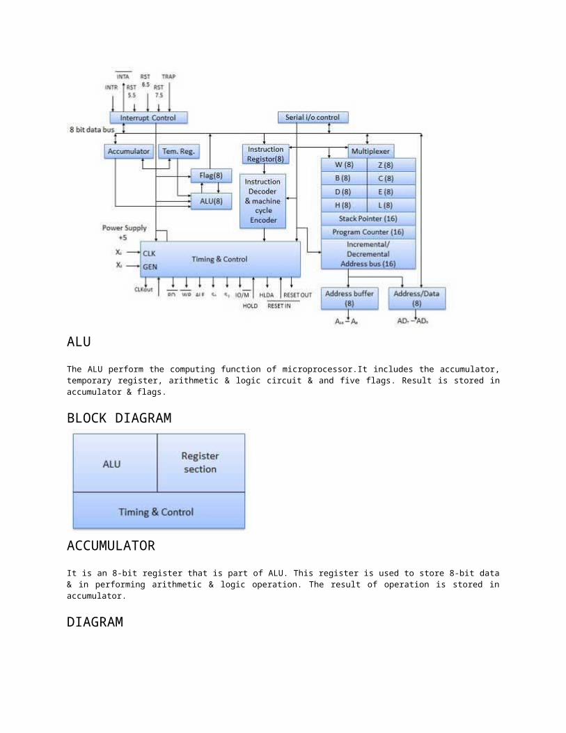
8085 MicroprocessorThe 8085 microprocessor is an 8-bit general purpose microprocessor which is capable to address 64k of memory. This processor has forty pins, requires +5 V single power supply and a 3-MHz single-phase clock.
BLOCK DIAGRAM
ALU
The ALU perform the computing function of microprocessor.It includes the accumulator, temporary register, arithmetic & logic circuit & and five flags. Result is stored in accumulator & flags.
BLOCK DIAGRAM
ACCUMULATOR
It is an 8-bit register that is part of ALU. This register is used to store 8-bit data & in performing arithmetic & logic operation. The result of operation is stored in accumulator.
DIAGRAM
FLAGS
The register are programmable. It can be used to store and transfer the data from the registers by using instruction. The ALU includes five flip-flops that are set & reset acc. to data condition in accumulator and other registers.
S (Sign) flag - After the execution of an arithmetic operation, if bit D7 of the result is 1, the sign flag is set. It is used to signed number. In a given byte, if D7 is 1 means negative number. If it is zero means it is a positive number.
Z (Zero) flag - The zero flag is set if ALU operation result is 0. AC (Auxiliary Carry) flag - In arithmetic operation, when carry is generated by digit D3 and passed on to digit D4, the
AC flag is set. This flag is used only internally BCD operation. P (Parity) flag - After arithmetic or logic operation, if result has even no. of 1s, the flag is set. If it has odd no. of 1s ,
flag is reset. C (Carry) flag - If arithmetic operation result in a carry, the carry flag is set, otherwise it is reset.
REGISTER SECTION
It is a basically storage device & transfer data from registers by using instruction.
Stack Pointer (SP) - The stack pointer is also a 16-bit register which is used as a memory pointer. It points to a memory location in Read/Write memory known as stack. In between execution of program, some time data to be stored in stack. The beginning of the stack is defined by loading a 16-bit address in the stack pointer.
Program Counter (PC) - This 16-bit register deals with fourth operation to sequence the execution of instruction. This register is also a memory pointer. Memory location have 16-bit address. It is used to store the execution address. The function of the program counter is to point to memory address from which next bytes is to be fetched.
Storage registers -- Thes registers store 8-bit data during a program execution. These register are identified as B,C,D,E,H,L. They can be combined as register pair BC, DE and HL to perform some 16 bit operations.
TIME AND CONTROL SECTION
This unit is responsible to synchronize Microprocessor operation as per the clock pulse and to generate the control signals which are necessary for smooth communication between Microprocessor and peripherals devices. The RD bar and WR bar signal are syncronous pulses which indicates whether data is available on the data bus or not.The control unit is responsible to control the flow of data between microprocessor, memory and peripheral devices.
PIN DIAGRAM
All the signal can be classified into six groups
S.N. Group Description
1 Address busThe 8085 microprocessor has 8 signal line, A15 - A8 which are unidirectional & used as a high order address bus.
2 Data busThe signal line AD7 - AD0 are bidirectional for dual purpose. They are used as low order address bus as well as data bus.
3 Control signal and Status signalControl Signal
RD bar - It is a read control signal (active low). It is active then memory read the data.WR bar - It is write control signal (active low). It is active when written into selected memory.
Status signal
ALU (Address Latch Enable) - When ALU is high. 8085 microprocessor is use address bus. When ALU is low. 8085 microprocessor is use data bus.IO/M bar - This is a status signal used to differentiate
between i/o and memory operation. When it is high, it indicate an i/o operation and low, it indicate memory operation.S1 and S0 - These status signal, similar to i/o and memory bar, can identify various operation, but they are rarely used in small system.
4 Power supply and frequency signal
Vcc - +5v power supply.Vss - ground reference.X, X - A crystal is connected at these two pins. The frequency is internally divided by two operate system at 3-MHz, the crystal should have a frequency of 6-MHz.CLK out - This signal can be used as the system clock for other devices.
5 Externally initiated signal
INTR(i/p) - Interrupt request.INTA bar (o/p) - It is used as acknowledge interrupt.TRAP(i/p) - This is non maskable interrupt and has highest priority.HOLD(i/p) - It is used to hold the executing program.HLDA(o/p) - Hold acknowledge.READY(i/p) - This signal is used to delay the microprocessor read or write cycle until a slow responding peripheral is ready to accept or send data.RESET IN bar - When the signal on this pin goes low, the program counter is set to zero, the bus are tri-stated, & MPU is reset.RESET OUT - This signal indicate that MPU is being reset. The signal can be used to reset other devices.RST 7.5, RST 6.5, RST 5.5 (Request interrupt) - It is used to transfer the program control to specific memory location. They have higher priority than INTR interrupt.
6 Serial I/O portsThe 8085 microprocessor has two signals to implement the serial transmission serial input data and serial output data.
Instruction FormatEach instruction is represented by a sequence of bits within the computer. The instruction is divided into group of bits called field. The way of instruction is expressed is known as instruction format. It is usually represented in the form of rectangular box. The instruction format may be of the following types.
Variable Instruction FormatsThese are the instruction formats in which the instruction length varies on the basis of opcode & address specifiers. For Example, VAX instruction vary between 1 and 53 bytes while X86 instruction vary between 1 and 17 bytes.
FORMAT
ADVANTAGE
These formats have good code density.
DRAWBACK
These instruction formats are very difficult to decode & pipeline.
Fixed Instruction FormatsIn this type of instruction format, all instruction are same size. For Example, MIPS, Power PC, Alpha, ARM.
FORMAT
ADVANTAGE
They are easy to decode & pipeline.
DRAWBACK
They don't have as good code density.
Hybrid Instruction FormatsIn this type of instruction formats, we have multiple format length specified by opcode.For example, IBM 360/70, MIPS 16, Thumb.
FORMAT
ADVANTAGE
These compromise between code density & instruction of these type are very easy to decode.
Addressing Modes
Addressing mode provide different ways for access an address to given data to a processor. Operated data is stored in the memory location, each instruction required certain data on which it has operate. There are various techniques to specify address of data. These technique are called Addressing Modes.
Direct addressing mode - In the direct addressing mode, address of the operand is given in the instruction and data is available in the memory location which is provided in instruction. We will move this data in desired location.
Indirect addressing mode - In the indirect addressing mode, the instruction specifies a register which contain the address of the operand. Both internal RAM and external RAM can be access via indirect addressing mode.
Immediate addressing mode - In the immediate addressing mode, direct data is given in the operand which move the data in accumulator. It is very fast.
Relative addressing mode - In the relative address mode, the effective address is determined by the index mode by using the program counter in stead of general purpose processor register. This mode is called relative address mode.
Index addressing mode - In the index address mode, the effective address of the operand is generated by adding a content value to the contents of the register. This mode is called index address mode.


