

This is a repository copy of Direct Digital Demultiplexing of Analog TDM Signals for Cable Reduction in Ultrasound Imaging Catheters..
White Rose Research Online URL for this paper:http://eprints.whiterose.ac.uk/100545/
Version: Accepted Version
Article:
Carpenter, TM, Rashid, MW, Ghovanloo, M et al. (3 more authors) (2016) Direct Digital Demultiplexing of Analog TDM Signals for Cable Reduction in Ultrasound Imaging Catheters. IEEE Transactions on Ultrasonics, Ferroelectrics and Freqency Control, 63 (8). pp. 1078-1085. ISSN 0885-3010
https://doi.org/10.1109/TUFFC.2016.2557622
(c) 2016 IEEE. Personal use of this material is permitted. Permission from IEEE must be obtained for all other users, including reprinting/ republishing this material for advertising orpromotional purposes, creating new collective works for resale or redistribution to servers or lists, or reuse of any copyrighted components of this work in other works.
[email protected]://eprints.whiterose.ac.uk/
Reuse
Unless indicated otherwise, fulltext items are protected by copyright with all rights reserved. The copyright exception in section 29 of the Copyright, Designs and Patents Act 1988 allows the making of a single copy solely for the purpose of non-commercial research or private study within the limits of fair dealing. The publisher or other rights-holder may allow further reproduction and re-use of this version - refer to the White Rose Research Online record for this item. Where records identify the publisher as the copyright holder, users can verify any specific terms of use on the publisher’s website.
Takedown
If you consider content in White Rose Research Online to be in breach of UK law, please notify us by emailing [email protected] including the URL of the record and the reason for the withdrawal request.
IEEE TRANSACTIONS ON ULTRASONICS, FERROELECTRICS, AND FREQUENCY CONTROL 1
Direct Digital Demultiplexing of
Analog TDM Signals for Cable Reduction
in Ultrasound Imaging CathetersThomas M. Carpenter, M. Wasequr Rashid, Maysam Ghovanloo,
David M. J. Cowell, Steven Freear, F. Levent Degertekin
Abstract—In real-time catheter based 3-D ultrasound imag-ing applications, gathering data from the transducer arrays isdifficult as there is a restriction on cable count due to thediameter of the catheter. Although area and power hungrymultiplexing circuits integrated at the catheter tip are used insome applications, these are unsuitable for use in small sizedcatheters for applications like intracardiac imaging. Further-more, the length requirement for catheters and limited poweravailable to on-chip cable drivers leads to limited signal strengthat the receiver end. In this paper an alternative approach usingAnalog Time Division Multiplexing (TDM) is presented whichaddresses the cable restrictions of ultrasound catheters. A noveldigital demultiplexing technique is also described which allowsfor a reduction in the number of analog signal processing stagesrequired. The TDM and digital demultiplexing schemes aredemonstrated for an intracardiac imaging system that wouldoperate in the 4-11MHz range. A TDM integrated circuit (IC)with 8x1 multiplexer is interfaced with a fast ADC through amicro-coaxial catheter cable bundle, and processed with an FPGARTL simulation. Input signals to the TDM IC are recoveredwith -40dB crosstalk between channels on the same micro-coax,showing the feasibility of this system for ultrasound imagingapplications.
Index Terms—TDM, ICE, FPGA, CMUT, CMUT-on-CMOS,Catheter
I. INTRODUCTION
CATHETER based real-time 3D imaging, such as used in
3-D transesophageal echography (TEE), requires data to
be captured from many transducer elements simultaneously
to avoid motion artefacts [1]. Direct connection to each of the
elements in the 2-D arrays is either impossible or very limiting
due to size of the catheter, especially in the case of small sized
catheters for intracardiac echography (ICE) [2]. It is partially
because of these limitations that current 3D ICE probes do
not have a large field of view [3]. Furthermore, current ICE
This research was sponsored by the National Institutes of Health underGrant No: U01 HL121838.
T. M. Carpenter is with the G.W. Woodruff School of Mechanical Engi-neering, Georgia Institute of Technology, Atlanta, GA 30332, USA (e-mail:[email protected]).
M. Wasequr Rashid and Maysam Ghovanloo are both with the School ofElectrical & Computer Engineering, Georgia Institute of Technology, Atlanta,GA 30332, USA (e-mail: [email protected])
F.L. Degertekin is with both the G.W. Woodruff School of MechanicalEngineering and School of Electrical & Computer Engineering, GeorgiaInstitute of Technology, Atlanta, GA 30332, USA
D. M. J. Cowell and S. Freear are both with the School of Electronic &Electrical Engineering, University of Leeds, Leeds, West Yorkshire, LS2 9JT,United Kingdom.
and TEE catheters are used in conjunction with harmful X-ray
imaging (fluoroscopy) for navigation [4].
To realize an ICE catheter that can be used under MRI
guidance avoiding ionizing radiation, the cable count needs to
be reduced significantly so as to reduce RF induced heating
of the metal conductors [5]. Therefore, cable reduction tech-
niques with electronics complexity, area, and power require-
ments suitable for integration at the tip of an ICE catheter
would have a significant impact in catheter based ultrasound
imaging applications, both in terms of implementing large
field of view ICE catheters, and by eliminating the need for
fluoroscopy. These techniques can then be implemented using
monolithic CMUT-on-CMOS, or ICs integrated with CMUT
or piezoelectric transducer arrays in a multi-chip package [6]
[7] [8] [9].
In this paper, a TDM approach with relatively simple
electronics on the catheter tip along with a direct digital
modulation scheme at the back end for signal recovery is
demonstrated. After a review of channel multiplexing methods
motivating the need for this approach, details of the TDM
system are presented along with the IC implementation in
CMOS. Real-Time Direct Digital Demodulation (DDD) as
realized in an FPGA is described and finally experimental
results on the overall system are presented.
II. CHANNEL MULTIPLEXING METHODS
In developing the proposed TDM scheme, several methods
for reducing cable count were considered. Using on-chip
digital multiplexing techniques would provide a method of
reducing cable count while maintaining signal integrity as a
digital output would be less prone to noise than transmitting
the observed echo responses directly. However, such a system
would require Analog to Digital (A/D) conversion of the
signals individually for every receiver element. While research
into lower power and smaller size ADCs continues [10], even
with the current state of the art technologies, for example a
35MSPS SAR ADC consuming 54mW of power and using
0.239mm2 area [11], having one ADC per element on-chip for
a 96 element transducer would still use upwards of 22mm2
area and consume over 5W of power. In a size and power
constrained system, such as an imaging catheter, this would
be simply unfeasible to implement.
Another approach, which has been demonstrated in [12] [13]
[14] [15] and [16], involves performing partial beamforming

2 IEEE TRANSACTIONS ON ULTRASONICS, FERROELECTRICS, AND FREQUENCY CONTROL
(µ-Beamforming) with analog delay chains in the transducer.
By performing delay-sum beamforming in the transducer,
fewer cables are required as the raw signals from every ele-
ment do not need to be transferred to front end for processing.
This approach requires a large number of capacitors and
switches for each channel in order to achieve the required
analog delays, which makes it unsuitable for systems with
size restrictions. This method would also be incompatible
with systems which make use of advanced imaging techniques
requiring all of the echo raw data.
A third approach for cable reduction is Frequency Division
Multiplexing (FDM) [17]. One such method of FDM, using
Analog Modulation (AM) has been shown to be feasible for
ICE applications and could be applicable to other ultrasound
applications. This design uses AM to multiplex multiple
signals on to each cable allowing all of the raw data to be
transferred by making better use of the channel bandwidth.
However this approach requires multiple analog filters and
mixers to produce the multiplexed output. Compact imple-
mentations of these electronic circuits on silicon are sensitive
to silicon process variations which means using the technique
in applications with hundreds of elements would be difficult
to ensure uniformity across all channels. Furthermore, FDM
would also require complex digital signal processing hardware
and software to demodulate and recover the signals prior to
image reconstruction, especially if real-time imaging or high
element counts are required.
Multiplexing the channels in time is also a possibility
for reducing the cable count for the system. The approach
allows multiple channels to share the same cable by assigning
each channel a time slot in which to transmit. Time-Division
Multiplexing (TDM) can be performed using many schemes,
the versatility and simplicity of which has resulted in extensive
use in communications and telephony applications [18] [19]
[20], and also for applications in ultrasound systems.
An approach with potential for small area, low element
count ultrasound applications is to convert the analog data
directly to a digital PWM signal, encoding the analog voltage
as the duty cycle – essentially performing on-chip digitiza-
tion without the need for an ADC [21]. The downside of
this approach is the massive bandwidth requirements for the
transmission channel when scaled to larger element counts.
The bandwidth is directly proportional to not only the number
of elements, and the sampling frequency, but also increases
exponentially to the number of bits of analog resolution
required. A system with 16 transducer elements each sampled
at 20MSPS with a 10bit resolution would require over 300GHz
of bandwidth to send down a single cable, which is simply not
feasible.
Analog TDM requires a relatively small amount of hardware
at the transmitter compared with the other schemes discussed
here. At the bare minimum, only an analog multiplexer and
simple digital counting logic is required to multiplex analog
data streams. The sequencing approach of the transducer
elements can be varied, allowing for different options in
assigning time slots based on the application.
In one approach the time slots are assigned on a per-firing
basis whereby each element in the array is connected to the
cable for a full firing. On each subsequent firing the next
element is connected, and so on until data for each element
has been collected. This approach is has been demonstrated in
several systems [22] [23] [24]. While this approach does allow
for cable reduction, it requires multiple firings to collect the
information as only one element per cable can be sampled in
a given firing. For very high element counts this will reduce
the maximum possible frame rate for imaging, and can lead to
more prominent motion artefacts as the time over which the
image is collected is increased.
In cases where data must be collected for all channels
simultaneously, perhaps due to high element counts, or if
high frame rates are required, the multiplexing scheme can
be designed so that the time slots are made short enough that
each channel can be sampled at above the Nyquist rate. In this
approach, rather than changing channel on each firing, instead
the multiplexer scans through every element in turn using a
sampling clock which is at least n times the Nyquist rate
(where n is the number of channels). This approach was briefly
presented in [25] in which 12 channels were multiplexed onto
a single cable using this technique. The approach has since
been demonstrated in [26] and [27] in which 8:1 and 4:1
reduction in cable counts were achieved respectively.
III. SIMULTANEOUS COLLECTION TDM SCHEME
In this paper, the TDM approached for simultaneous collec-
tion of data from all elements is discussed in detail, building
on the system demonstrated in [26]. There are two key areas
of focus, the multiplexing electronics which would be located
with the transducer, and the direct digital demultiplexing
design which makes up the receiver.
A minimal TDM transmit system requires only an analog
multiplexer and a buffer for each channel and so requires
much less space to implement than the other channel reduction
schemes considered. At the receiver end the signals then
need to be demultiplexed which requires additional hardware.
If done in the analog domain this would require the high
frequency multiplexed signals to be passed through a syn-
chronous demultiplexer, filtered, and then passed into an ADC
dedicated to each channel. Each of these stages would add
noise to the system, would present additional complexity in
matching the circuits across all channels, and would require a
large number of ADCs.
As there is now increasingly widespread availability of very
high speed ADCs with effective number of bits on the order of
10 or more [28] [29], and also FPGAs capable of performing
complex DSP functions on many channels in parallel, much of
the receiver hardware complexity can be eliminated by moving
all of the demultiplexing requirements from the analog domain
into an FPGA and allowing demultiplexing to be done directly
in the digital domain.
The clock frequency of the multiplexer will be much higher
than the sampling frequency for each channel, in an 8 channel
25MSPS design as an example, the clock frequency would be
200MHz. The analog signals are modulated onto pulses which
must rise and stabilize fast enough that the amplitude can be
extracted by the ADC correctly. The cables connecting the

CARPENTER et al.: DIRECT DIGITAL DEMULTIPLEXING OF ANALOG TDM SIGNALS FOR CABLE REDUCTION IN ULTRASOUND IMAGING CATHETERS 3
Mux Buf. Coax
Cable
(f x n) MHz Clock
n
f MSPS
S/HLNA TGC1
... Demultplexer,
Interpolation,
Phase Correction,
BeamformerJESD204B
n
AFE CMOS Electronics ‘n’ = Number of Channels (TDM Factor)
φo
S/HLNA TGC
LNA ADC
Clock
Gen.
(f x n) MHz Clock
(f x n) MSPS
Counter
Stratix V
FPGA
‘f ’ = Sample Rate per Channel
Fig. 1. Analog TDM Scheme using Direct Digital Demultiplexing - AFE CMOS IC Placed with Transducer Array to Multiplex Signals
multiplexer and ADC need sufficient bandwidth to limit the
amount of distortion of the high frequency TDM signals.
In Fig. 1 an overview of the simplified TDM scheme
is shown. The receiver end consists only of an LNA and
ADC in the analog path, which is then followed by an
FPGA to perform the digital demultiplexing. The transmitter
end consists of an analog front end (AFE) followed by a
sample and hold (S/H) capacitor for each channel, each of
which is then connected to an analog multiplexer. The Time-
Gain Compensation (TGC) in the AFE can be controlled
via a single cable to digitally cycle through fixed levels, or
alternatively controlled using an analog reference signal for
finer adjustment.
The multiplexing is controlled by digital circuitry which
generates sample clocks for each channel, and control signals
for the multiplexer. This circuitry is controlled by a clock
signal generated by the receiver and transmitted over an
additional cable. The ADC clock is synchronized to this same
clock signal to ensure that each ADC sample corresponds
exactly to one channel in the multiplexed data. As a result
of this synchronization, demultiplexing theoretically becomes
a simple task of separating the data into groups consisting of
every nth sample.
IV. MIXED SIGNAL MULTIPLEXER DESIGN
The multiplexing circuitry is to be placed with the trans-
ducer to receive the signals and connect them with a reduced
number of connections to the back end electronics. To directly
interface with the transducers an AFE is required which
is suited to the technology. For example a Transimpedance
Amplifier (TIA) based AFE would be suitable for CMUT
designs [22]. Also required is an anti-aliasing filter prior
to the signals being sampled. Additional electronics such as
integrated TX/RX switches may also be needed in the front
end.
Following the AFE is the sampling circuitry. This consists
of a sample and hold buffer, an analog multiplexer, and
sequencing logic. An overview of this is shown in Fig. 2. The
sequencing logic generates sample clock and multiplexer select
signals for each channel based on a counter which keeps track
of which channel is to be connected. The sequencing signals
are demonstrated in Fig. 3.
Buf.
Grey CodeCounter
S/H
S/H
Sample Select
Mux
SequencingLogic
TDM Clock
Link TrainingMode Select
Mux Select
Fig. 2. TDM Multiplexer Design and Control Signaling
Ch 1
Ch 2
Ch N
...
Mux Select
Sample Sel.
Sample/Hold + Mux
(a) (b)
Fig. 3. Control Signal Timing for (a) Sample/Hold and (b) Multiplexer
When a given channel is not being driven on to the cable,
the S/H capacitor is connected via a pass transistor to the
output of the TGC. This gives time for the capacitor to match
the signal voltage and sample the signal (Fig. 3a). Once it is
time for that channel to be connected to the output, the S/H
capacitor is disconnected from the input, and after a short dead
time, is then connected via a buffer and the multiplexer to the
cable driver (Fig. 3b).
The S/H circuitry has been included in the transmitter
to ensure the signals are correctly sampled and transmitted.
Sampling in the transmitter ensures that during each time
period on the cable, a constant value is sent. This means that
the high speed cable driver can settle to a constant value after a
short switching transient rather than having to precisely follow
a time varying signal during each period. This should ensure
that an accurate sample is quantized by the ADC for that time
period.
4 IEEE TRANSACTIONS ON ULTRASONICS, FERROELECTRICS, AND FREQUENCY CONTROL
1 2 N 1...+V
-V
ADC Clock TDM Clock
φL
φO
φR
(a) (b)
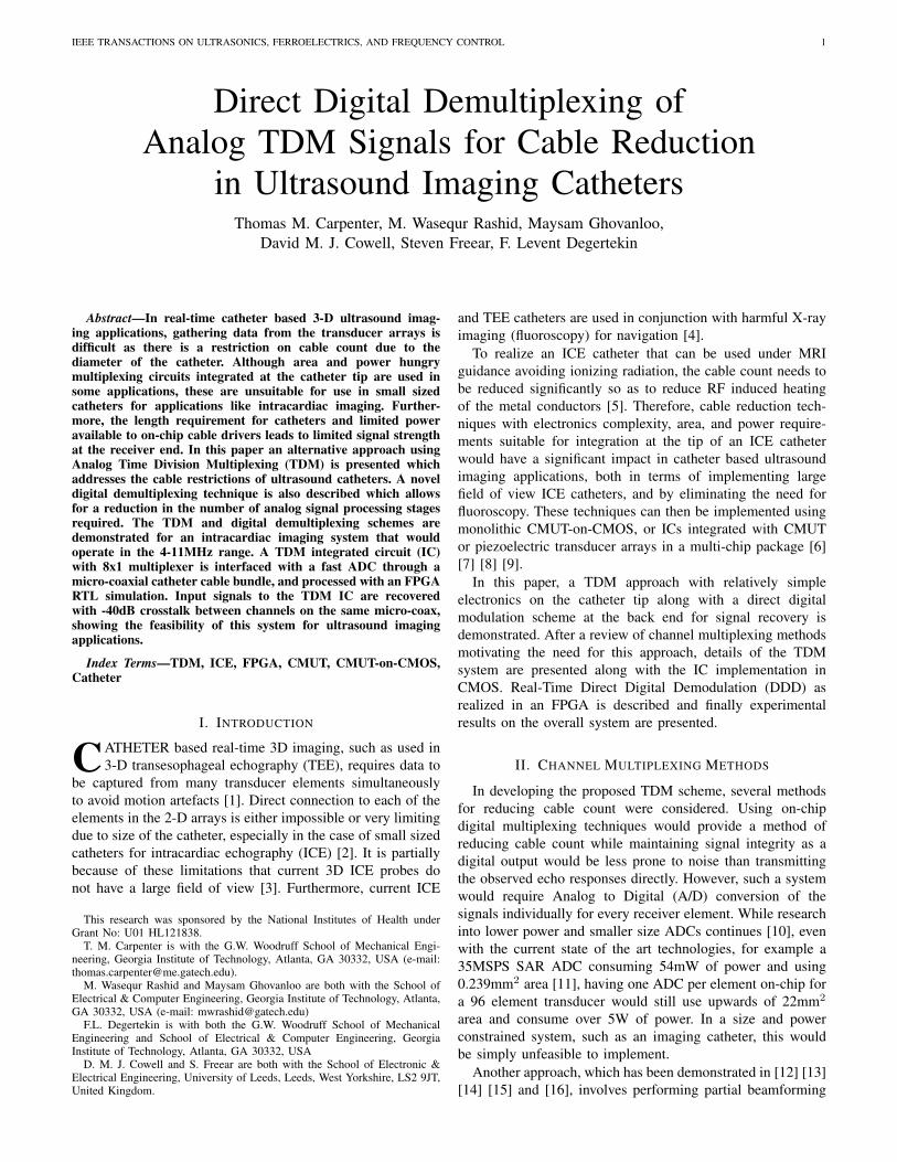
Fig. 4. (a) Link Training Waveform to Locate First Multiplexer Channel(b) Edge Detection Scheme Used for Phase Alignment
A key part of the TDM scheme is alignment between the
ADC and the multiplexer. Two types of alignment are required
to ensure that the samples are correctly digitized: channel
alignment and phase alignment. The former is required to
ensure the sample for channel 1 on the multiplexer is known
to be channel 1 when demultiplexing – without this alignment
the elements could get mixed up during demultiplexing. The
latter is used to ensure that the TDM and ADC clocks are
correctly phase aligned to account for propagation delays in
the cabling. This phase alignment is critical to ensure the ADC
is taking samples when the signal on the cable has stabilized
rather than during switching transients.
Both alignment requirements are satisfied during an initial-
ization sequence which consists of a training pattern being
generated by the multiplexer and analyzed in the FPGA.
During the training sequence, the inputs to the multiplexer are
internally tied to bias voltages, with the first channel connected
to one voltage level, and all other channels connected to a
second voltage level as shown in Fig. 4. By analyzing the
converted data it is possible to correctly align the system.
The alignment starts with channel 1 being identified by
way of the quantized codes being significantly different in one
sample than the others as illustrated in Fig. 4a. After this the
phase of the TDM clock is adjusted to find the optimal phase
shift between the ADC and TDM clocks. The TDM clock
phase can be adjusted using a Phase-Locked Loop (PLL) in
the FPGA to determine the optimum alignment, as shown in
Fig. 4b. Initially the phase shift is increased to locate the point
at which the difference between channel 1 and the others is
reduced by half, ΦL. The phase difference is then reduced
until the point at which the difference drops to the same
amount, ΦR. These two points identify at which phases the
switching transients are occurring, so the optimal phase where
the sampling should be performed, ΦO, must be the midpoint.
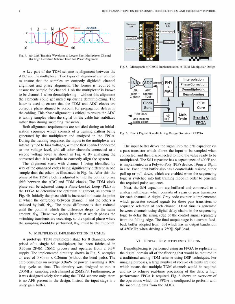
V. MULTIPLEXER IMPLEMENTATION IN CMOS
A prototype TDM multiplexer stage for 8 channels, com-
prised of a single 8:1 multiplexer, has been fabricated in
0.35µm 2P4M TSMC process and operates from a 3.3V
supply. The implemented circuitry, shown in Fig. 5, occupies
an area of 0.80mm x 0.26mm (without the bond pads). The
chip consumes on average 3.9mW of power, assuming a 10%
duty cycle on time. The circuitry was designed to run at
200MHz, sampling each channel at 25MSPS. Furthermore, as
it was designed solely for testing the TDM scheme only, there
is no AFE present in the design. Instead the input stage is a
unity gain buffer.
Input Buers
Output Buer
Sample/Hold
Sequencing Logic
Transducer
Side
Cable
Side
1½
1
½
(mm)
Fig. 5. Micrograph of CMOS Implementation of TDM Multiplexer Design
LinkTrain
PHY+
MAC
TDM Clock
Link TrainingMode Select
Interpolation
Phase Correction
Demultiplexing
Beamforming
JESD204BLNA ADC
Clock
Gen.
Stratix V
FPGA
LNA
Balun +Z-Match
ADC
DigitiseTDM
φo
PLL
PCIe
Core
Fig. 6. Direct Digital Demultiplexing Design Overview of FPGA
The input buffer drives the signal into the S/H capacitor via
a pass transistor which allows the input to be sampled when
connected, and then disconnected to hold the value ready to be
multiplexed. The S/H capacitor has a capacitance of 400fF and
is implemented as a Poly-to-Poly (PIP) device, 19µm x 19µm
in size. Each input buffer also has a controllable resistor, either
pull-up or pull-down, which are enabled when the sequencing
logic is switched into link training mode in order to generate
the required pulse sequence.
Next, the S/H capacitors are buffered and connected to a
analog multiplexer which consists of a pair of pass transistors
for each channel. A digital Gray code counter is implemented
which generates control signals for these pass transistors to
sequence selection of each channel. Dead time is generated
between channels using digital delay chains in the sequencing
logic to delay the rising edge of the control signal separately
from the falling edge. The final output stage is a current feed-
back buffer adopted from [30] which has an output bandwidth
of 450MHz when driving a 75Ω||15pF load.
VI. DIGITAL DEMULTIPLEXER DESIGN
Demultiplexing is performed using an FPGA to replicate in
the digital domain all of the filtering that would be required in
a traditional analog TDM scheme using DSP techniques. For
imaging purposes, a large number of receive elements are used
which means that multiple TDM channels would be required
and so to achieve real-time processing of the data, a high
performance FPGA is required. Fig. 6 shows an overview of
the operations which the FPGA is configured to perform with
the incoming data from the ADCs.
CARPENTER et al.: DIRECT DIGITAL DEMULTIPLEXING OF ANALOG TDM SIGNALS FOR CABLE REDUCTION IN ULTRASOUND IMAGING CATHETERS 5
The firmware has been designed to interface with the high
speed ADCs required for the TDM scheme, to complete link
training, and to perform demultiplexing. The firmware must
also beamform the data streams and to transfer images to
a display. In the case of this design, the ADC interface is
performed using the JESD204b protocol, which is a recently
standardized protocol [31] becoming common with high speed
ADCs. By using a standard interface, then if a higher sample
rate or channel count is required, faster ADCs (or more of
them) can be simply substituted in to the design. Transfer of
image data is also done using a standardized protocol, in this
case a PCIe link to a workstation computer from which images
can be displayed, or further processing such as 3D rendering
can be performed.
One of the key roles for the FPGA is demultiplexing the
TDM streams. This on the face of it should be a simple task,
basically a case of taking each sample from the ADC and
splitting it apart on a cyclic basis so that every n samples con-
tains one sample for each of the different channels. However
the task is actually somewhat more complex due to the way in
which the channels are sampled by the multiplexer. Referring
back to Fig. 3a, it is apparent that the samples for each channel
are not taken simultaneously. While each channel is sampled
at the same rate, there is a 45 phase shift from channel to
channel - in fact for any multiplexing factor n, the phase shift
between channels will be 360 divided by n. This is done to
minimize the multiplexer circuit size and to ensure that each
sample once taken is immediately driven to the cable rather
than being held in a leaky capacitor for longer than necessary.
Correction of the channel to channel phase shift must be
performed before beamforming can take place. If the data
streams were directly summed, the phase shift would act as
an unwanted beamforming delay which would be different for
each channel. The phase shift must be removed for correct
reconstruction, however to do so would require the data to
be shifted in the digital domain by less than one sample, a
fractional delay, which is difficult to remove [32].
The method used in this design approach is to perform
interpolation of the data up to the TDM clock rate using a
multi-rate interpolation FIR filter. Once at the TDM clock rate,
the required phase shifts become an integer number of samples
where the length depends on the channel – the first channel is
delayed by 1 cycle, the second by 2 cycles, and so on. With
the delays in place, all channels in the interpolated stream will
have been realigned and the phase shift from the multiplexer
removed. The resulting data stream can then be demultiplexed
and, if required, decimated to reduce the volume of data.
The demultiplexer design has been developed primarily
using Verilog HDL and Qsys (Altera). From this design,
an RTL (Register-Transfer Level) simulation model has been
generated to allow for design verification and also to allow
test processing of data without the need for physical FPGA
hardware. The design has also been synthesized to verify that
it can be implemented in an FPGA. The design has been
built around a Stratix V GS FPGA (5SGSMD5K2F40C2N)
from Altera. Using a test design for a 96 channel receiver (12
cables), all of the required hardware can be fit into the design,
utilizing roughly 70% of the resources of the FPGA, and
Chip Carrier
200MHz Clock Input
ADC - TI ADC16DX370
1m µCoax Cable
Low Noise Amp.
Fig. 7. Equipment Setup for Testing TDM Multiplexing and ADC CaptureDemultiplexing is Performed using RTL Simulation of FPGA
capable of achieving a maximum clock frequency of around
350MHz - more than sufficient for a 200MHz TDM clock
rate. The TDM clock PLL can run with a Voltage-Controlled
Oscillator (VCO) frequency of 1.6GHz which would afford a
phase resolution of 78.125ps when adjusting the clock phase
during link training.
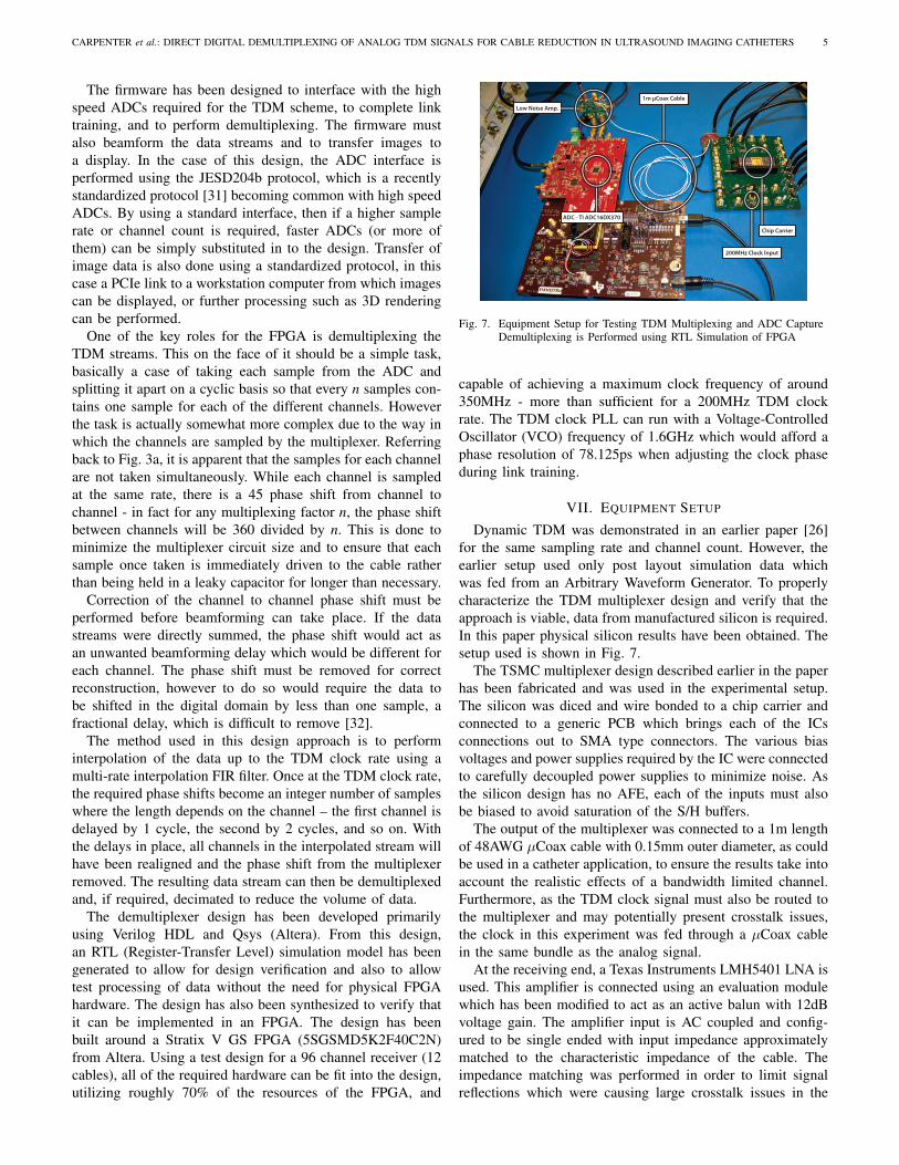
VII. EQUIPMENT SETUP
Dynamic TDM was demonstrated in an earlier paper [26]
for the same sampling rate and channel count. However, the
earlier setup used only post layout simulation data which
was fed from an Arbitrary Waveform Generator. To properly
characterize the TDM multiplexer design and verify that the
approach is viable, data from manufactured silicon is required.
In this paper physical silicon results have been obtained. The
setup used is shown in Fig. 7.
The TSMC multiplexer design described earlier in the paper
has been fabricated and was used in the experimental setup.
The silicon was diced and wire bonded to a chip carrier and
connected to a generic PCB which brings each of the ICs
connections out to SMA type connectors. The various bias
voltages and power supplies required by the IC were connected
to carefully decoupled power supplies to minimize noise. As
the silicon design has no AFE, each of the inputs must also
be biased to avoid saturation of the S/H buffers.
The output of the multiplexer was connected to a 1m length
of 48AWG µCoax cable with 0.15mm outer diameter, as could
be used in a catheter application, to ensure the results take into
account the realistic effects of a bandwidth limited channel.
Furthermore, as the TDM clock signal must also be routed to
the multiplexer and may potentially present crosstalk issues,
the clock in this experiment was fed through a µCoax cable
in the same bundle as the analog signal.
At the receiving end, a Texas Instruments LMH5401 LNA is
used. This amplifier is connected using an evaluation module
which has been modified to act as an active balun with 12dB
voltage gain. The amplifier input is AC coupled and config-
ured to be single ended with input impedance approximately
matched to the characteristic impedance of the cable. The
impedance matching was performed in order to limit signal
reflections which were causing large crosstalk issues in the

6 IEEE TRANSACTIONS ON ULTRASONICS, FERROELECTRICS, AND FREQUENCY CONTROL
earlier paper. The output of the amplifier was configured to
be fully differential and connected directly to the input of a
high speed ADC – a TI ADC16DX370EVM board. The ADC
has an input bandwidth of 800MHz, and a 16bit resolution of
which approximately 10bits of resolution is used, though this
will depend on the amplitude of the transducer signals.
As the hardware for interfacing the FPGA to the ADC has
not yet been implemented, the data from the ADC has been
captured using an evaluation module which interfaces the ADC
with a PC via USB. The link training was performed by man-
ually adjusting the phase between the ADC and TDM clocks
which were produced by two high speed signal generators
with a common reference clock. To complete the chain, the
demultiplexing and processing of the data has been performed
using the simulation model that was generated from the FPGA
firmware design. The simulation model will exhibit exactly the
same behavior as the targeted FPGA will, which makes the
model a perfectly valid tool for processing experimental data.
For this design, a 200MHz clock signal is used, which
means that each of the 8 channels is sampled at 25MSPS prior
to being multiplexed. The frequency was chosen as a trade-off
between sampling rate and the bandwidth requirements of the
cable.
VIII. RESULTS AND COMPARISONS
Using the setup explained in VII, several experiments were
performed in order to characterize the TDM silicon and the
system as a whole. Of specific interest are two key points,
firstly can ADC be synchronized correctly to allow the signals
feeding the input of the TDM IC to be recovered using
the direct digital demultiplexing approach, and secondly to
determine how much crosstalk is present between channels
as a result of distortion of the multiplexed signal through the
cable.
During each test, signal generators were used to feed signals
into either one channel, or multiple channels (with other
channels receiving DC). Specifically, the tests involved using
either a simple tone signal, or a more realistic sinc pulse.
Using a tone allows for any crosstalk to be easily identified
by analyzing the spectrum of each recovered signal – a spike
at the frequency of the tone indicates that crosstalk is present.
The sinc pulse allows for seeing the response of the system
over the full bandwidth of each channel.
Fig. 8 shows the results from one of the experiments, in
which only channel 1 of the eight was fed a signal, and the
others tied to a DC bias. Fig. 8a and Fig. 8b show the recovered
signal for the case of a 7MHz tone, both in the time and
frequency domain – the results are from the output of the
FPGA simulation, which after the interpolation and decimation
performed by the FPGA, are sampled at 50MSPS. Fig. 8c and
Fig. 8d show the recovered signal for the case of a sinc pulse
with a bandwidth of approximately 11MHz, again both in the
time and frequency domain.
As seen from Fig. 8a, the tone has clearly been recovered in
the demultiplexing process, with the FFT of the signal showing
a clear spike at 7MHz. There is some crosstalk occurring
between channels as evidenced by the 7MHz spike in Fig. 8b
on the other channels which should have no signal. The level
of the crosstalk signals is less than -40dB when compared
to the signal on channel 1. It should be noted that this is
a measurement of the crosstalk between signals in the same
µCoax cable as a result of the multiplexing scheme. The
electrical crosstalk between the two separate µCoax cables
in a catheter bundle was measured to be below -60dB at
frequencies up to 600MHz, therefore it is the TDM crosstalk
which represents the limiting factor in this scheme.
The frequency domain also shows clear spikes present at
3MHz, 4MHz, and 11MHz, with smaller spikes at 8MHz
and 10MHz also. It seems plausible that they are caused by
aliasing within the multiplexer. For example, if the 7MHz tone
feeding the IC had some signal present at the second and third
harmonics, this would account for two of the spikes (4MHz
and 11MHz) as a result of aliasing. Investigation of into the
cause of these spikes was not complete at the time the paper
was submitted.
Observing the signal recovered from feeding in a sinc pulse,
Fig. 8c, the signal has also clearly been recovered correctly,
with a fairly flat response across the pass band of the spectrum.
The signals are band-pass filtered in the FPGA with cut-off
frequencies of 3MHz and 10MHz resulting in the relatively
empty spectrum outside this band. It is difficult to determine
from the frequency domain in Fig. 8d what level of crosstalk
is present between channels, however by measuring the peaks
in the time domain, this crosstalk is roughly -36dB – similar
levels to the tone test.
These results show a significant improvement over those
of the earlier work [26]. The source of this improvement is
almost certainly the result of changes made at the receiving
end, specifically the inclusion of an amplifier that has an input
impedance closely matched to the characteristic impedance of
the cable. This matching helps to reduce the amount of signal
reflection in the cable which is one of the major sources of
crosstalk between channels.
The crosstalk levels still appear to be large. However it
is important to place these results in the context of the
application. In a practical ultrasound imaging system, the
input of the multiplexer would be connected to a transducer
array in which each channel on the same multiplexer is an
adjacent element. The variation in signal on adjacent channels
of the multiplexer is much less than in these tests and as a
result the channel to channel crosstalk can be significantly
less. Furthermore, even at the presented crosstalk levels, the
system would still provide suitable performance for ultrasound
imaging catheters [33].
IX. CONCLUSIONS
To produce 3-D ICE catheters with large element counts,
cable reduction is a key requirement not only to minimize the
catheter diameter but also to allow operation under MRI where
the risk of burns from induced heating in cables is a concern.
While there are currently a large variety of cable reduction
strategies, many of these are not suitable for this application
due to size, power, or other limitations.
Time-division multiplexing coupled with direct digital de-
multiplexing presents an alternative reduction strategy which

CARPENTER et al.: DIRECT DIGITAL DEMULTIPLEXING OF ANALOG TDM SIGNALS FOR CABLE REDUCTION IN ULTRASOUND IMAGING CATHETERS 7
(a) 7MHz Tone Demultiplexed from TDM and Interpolated to 50MSPS (b) FFT of 7MHz Tone Showing Crosstalk Levels
(c) Sinc Pulse Demultiplexed from TDM and Interpolated to 50MSPS (d) FFT of Sinc Pulse Showing Available Bandwidth
Fig. 8. Digitally Demultiplexed Experimental Results
is well suited to the requirements of ultrasound catheters. This
TDM approach has been developed and demonstrated in this
paper. In the system design a cable reduction ratio of at least
8:1 can be achieved whilst allowing for simultaneous sampling
of echo signals by sampling a time multiplexed signal at a very
high sample rate. The signals were then in the digital domain
using DSP techniques in RTL simulation of firmware for a
high performance FPGA.
Experimental results have been obtained using a CMOS
multiplexer fabricated in a 0.35µm process coupled with a
1m length of narrow diameter µCoax cable and a high-speed
ADC, and have been presented. These results demonstrate that
the design is able to achieve a crosstalk between channels on
the same cable of about -40dB. This suggests the approach
could provide suitable performance in an ultrasound imaging
catheter while significantly reducing cable count.
REFERENCES
[1] L. Sugeng, S. K. Shernan, I. S. Salgo, L. Weinert, D. Shook, J. Raman,V. Jeevanandam, F. Dupont, S. Settlemier, B. Savord, J. Fox, V. Mor-Avi,and R. M. Lang, “Live 3-dimensional transesophageal echocardiographyinitial experience using the fully-sampled matrix array probe,” J Am Coll
Cardiol., vol. 52, no. 6, pp. 446–449, Aug 2008.
[2] D. E. Dausch, K. H. Gilchrist, J. B. Carlson, S. D. Hall, J. B. Castellucci,and O. T. von Ramm, “In vivo real-time 3-D intracardiac echo usingPMUT arrays,” IEEE Transactions on Ultrasonics, Ferroelectrics, and
Frequency Control, vol. 61, no. 10, pp. 1754–1764, Oct 2014.
[3] N. Brysiewicz, T. Mitiku, K. Haleem, P. Bhatt, M. Al-Shaaraoui,J. F. Clancy, M. A. Marieb, L. Sugeng, and J. G. Akar, “3D Real-Time Intracardiac Echocardiographic Visualization of Atrial StructuresRelevant to Atrial Fibrillation Ablation,” J Am Coll Cardiol., vol. 7,no. 1, pp. 97–100, Jan 2014.
[4] K. Ralovich, M. John, E. Camus, N. Navab, and T. Heimann, “6DoFCatheter Detection, Application to Intracardiac Echocardiography,”in 2014:17th International ConferenceMedical Image Computing and
Computer-Assisted Intervention, vol. 8674, 2014, pp. 635–642.
[5] M. F. Dempsey, B. Condon, and D. M. Hadley, “Investigation ofthe factors responsible for burns during MRI,” Journal of Magnetic
Resonance Imaging, vol. 13, no. 4, pp. 627–631, 2001.
[6] G. Gurun, C. Tekes, J. Zahorian, T. Xu, S. Satir, M. Karaman, J. Hasler,and F. L. Degertekin, “Single-chip CMUT-on-CMOS front-end systemfor real-time volumetric IVUS and ICE imaging,” IEEE Transactions on
Ultrasonics, Ferroelectrics, and Frequency Control, vol. 61, no. 2, pp.239–250, February 2014.
[7] A. Bhuyan, J. W. Choe, B. C. Lee, I. Wygant, A. Nikoozadeh,O. Oralkan, and B. T. Khuri-Yakub, “3D volumetric ultrasound imagingwith a 32x32 CMUT array integrated with front-end ICs using flip-chipbonding technology,” in 2013 IEEE International Solid-State Circuits
Conference Digest of Technical Papers (ISSCC), Feb 2013, pp. 396–397.
[8] A. Moini, A. Nikoozadeh, O. Oralkan, J. W. Choe, A. F. Sarioglu, D. N.Stephens, A. de La Rama, P. Chen, C. Chalek, A. Dentinger, D. Wildes,L. S. Smith, K. Thomenius, K. Shivkumar, A. Mahajan, M. O’Donnell,D. J. Sahn, and P. T. Khuri-Yakub, “Volumetric intracardiac imagingusing a fully integrated CMUT ring array: Recent developments,” in2011 IEEE International Ultrasonics Symposium (IUS), Oct 2011, pp.692–695.
[9] Y. Lu, H. Tang, S. Fung, Q. Wang, J. M. Tsai, M. Daneman, B. E. Boser,and D. A. Horsley, “Ultrasonic fingerprint sensor using a piezoelectricmicromachined ultrasonic transducer array integrated with complemen-tary metal oxide semiconductor electronics,” Applied Physics Letters,vol. 106, no. 26, 2015.
[10] B. Murmann. ADC Performance Survey 1997-2015. [Online]. Available:http://web.stanford.edu/ murmann/adcsurvey.html
[11] M. Krmer, E. Janssen, K. Doris, and B. Murmann, “15.7 14b 35MS/SSAR ADC achieving 75dB SNDR and 99dB SFDR with loop-embeddedinput buffer in 40nm CMOS,” in 2015 IEEE International Solid-State
Circuits Conference - (ISSCC), Feb 2015, pp. 1–3.
[12] B. Savord and R. Solomon, “Fully sampled matrix transducer for realtime 3D ultrasonic imaging,” in 2003 IEEE Symposium on Ultrasonics,vol. 1, Oct 2003, pp. 945–953 Vol.1.

8 IEEE TRANSACTIONS ON ULTRASONICS, FERROELECTRICS, AND FREQUENCY CONTROL
[13] G. Matrone, A. S. Savoia, M. Terenzi, G. Caliano, F. Quaglia, andG. Magenes, “A volumetric CMUT-based ultrasound imaging systemsimulator with integrated reception and µ-beamforming electronics mod-els,” IEEE Transactions on Ultrasonics, Ferroelectrics, and Frequency
Control, vol. 61, no. 5, pp. 792–804, May 2014.[14] T. K. Song and J. F. Greenleaf, “Ultrasonic dynamic focusing using
an analog FIFO and asynchronous sampling,” IEEE Transactions on
Ultrasonics, Ferroelectrics, and Frequency Control, vol. 41, no. 3, pp.326–332, May 1994.
[15] B. Stefanelli, I. O’Connor, L. Quiquerez, A. Kaiser, and D. Billet, “Ananalog beam-forming circuit for ultrasound imaging using switched-current delay lines,” IEEE Journal of Solid-State Circuits, vol. 35, no. 2,pp. 202–211, Feb 2000.
[16] Z. Yu, M. A. P. Pertijs, and G. C. M. Meijer, “Ultrasound beamformerusing pipeline-operated S/H delay stages and charge-mode summation,”Electronics Letters, vol. 47, no. 18, pp. 1011–1012, September 2011.
[17] M. W. Rashid, C. Tekes, M. Ghovanloo, and F. L. Degertekin, “Designof frequency-division multiplexing front-end receiver electronics forCMUT-on-CMOS based intracardiac echocardiography,” in 2014 IEEE
International Ultrasonics Symposium (IUS), Sept 2014, pp. 1540–1543.[18] K. Pahlavan and P. Krishnamurthy, “GSM and TDMA Technology,” in
Principles of Wireless Networks: A Unified Approach. Prentice Hall,2002, ch. 7, pp. 319–347.
[19] H. P. E. Stern, S. A. Mahmoud, and L. E. Stern, “MultiplexingTechniques,” in Communication Systems: Analysis and Design. PearsonPrentice Hall, 2004, ch. 7, pp. 362–387.
[20] D. M. Spirit, A. D. Ellis, and P. E. Barnsley, “Optical time divisionmultiplexing: systems and networks,” IEEE Communications Magazine,vol. 32, no. 12, pp. 56–62, Dec 1994.
[21] J. Lim, E. F. Arkan, F. L. Degertekin, and M. Ghovanloo, “Towarda reduced-wire readout system for ultrasound imaging,” in 2014 36th
Annual International Conference of the IEEE Engineering in Medicine
and Biology Society (EMBC), Aug 2014, pp. 5080–5084.[22] G. Gurun, P. Hasler, and F. L. Degertekin, “Front-end receiver electronics
for high-frequency monolithic CMUT-on-CMOS imaging arrays,” IEEE
Transactions on Ultrasonics, Ferroelectrics, and Frequency Control,vol. 58, no. 8, pp. 1658–1668, August 2011.
[23] C. Tekes, T. Xu, T. M. Carpenter, S. Bette, U. Schnakenberg, D. Cowell,S. Freear, O. Kocaturk, R. J. Lederman, and F. L. Degertekin, “Real-timeimaging system using a 12-MHz forward-looking catheter with singlechip CMUT-on-CMOS array,” in 2015 IEEE International Ultrasonics
Symposium (IUS), Oct 2015.[24] D. F. Lemmerhirt, A. Borna, S. Alvar, C. A. Rich, and O. D. Kripfgans,
“CMUT-in-CMOS 2D arrays with advanced multiplexing and time-gaincontrol,” in 2014 IEEE International Ultrasonics Symposium (IUS), Sept2014, pp. 582–586.
[25] C. Daft, S. Panda, P. Wagner, and I. Ladabaum, “Two Approaches toElectronically Scanned 3D Imaging Using cMUTs,” in IEEE Ultrasonics
Symposium, 2006, Oct 2006, pp. 685–688.[26] T. M. Carpenter, M. W. Rashid, M. Ghovanloo, D. Cowell, S. Freear,
and F. L. Degertekin, “Time-division multiplexing for cable reductionin ultrasound imaging catheters,” in 2015 IEEE Biomedical Circuits and
Systems Conference (BioCAS), Oct 2015.[27] Q. Liu, C. Chen, Z. yao Chang, C. Prins, and M. A. P. Pertijs, “A mixed-
signal multiplexing system for cable-count reduction in ultrasoundprobes,” in 2015 IEEE International Ultrasonics Symposium (IUS), Oct2015.
[28] B. Murmann, “A/D converter trends: Power dissipation, scaling and dig-itally assisted architectures,” in 2008 IEEE Custom Integrated Circuits
Conference, Sept 2008, pp. 105–112.[29] B. E. Jonsson, “A survey of A/D-Converter performance evolution,” in
2010 17th IEEE International Conference on Electronics, Circuits, and
Systems (ICECS), Dec 2010, pp. 766–769.[30] K. Manetakis, C. Toumazou, and C. Papavassiliou, “A 120 MHz, 12
mW CMOS current feedback opamp,” in Proceedings of the IEEE 1998
Custom Integrated Circuits Conference, May 1998, pp. 365–368.[31] Serial Interface for Data Converters, JEDEC Committee JC-16
Std., Jan 2012. [Online]. Available: http://www.jedec.org/standards-documents/results/jesd204
[32] T. I. Laakso, V. Valimaki, M. Karjalainen, and U. K. Laine, “Splittingthe unit delay [FIR/all pass filters design],” IEEE Signal Processing
Magazine, vol. 13, no. 1, pp. 30–60, Jan 1996.[33] C. Oakley, J. Mueller, D. Dietz, and J. Kuhnke, “A minimally invasive
ultrasound probe using non-coax cabling,” in 2001 IEEE Ultrasonics
Symposium, vol. 2, 2001, pp. 1011–1016 vol.2.
Thomas M. Carpenter received the M.Eng. de-gree in electronic and electrical engineering for theUniversity of Leeds in 2014. Following this, hejoined Georgia Institute of Technology, Atlanta as aresearch engineer developing high-speed FPGA de-signs for ultrasound imaging applications. He is alsoa visiting researcher with the ultrasound researchgroup at the University of Leeds. His main researcharea is embedded systems and FPGA design, bothin the biomedial field and for industrial applications.
M. Wasequr Rashid (S’10) received the B.Sc de-gree in electrical and electronics engineering fromBangladesh University of Engineering and Technol-ogy, Bangladesh, and the M.S. degree in electricaland computer engineering from New Mexico StateUniversity, Las Cruces, in 2004 and 2010, respec-tively. He is currently working towards the Ph.D.degree in electrical and computer engineering atGeorgia Institute of Technology, Atlanta. His currentresearch interests include mixed-signal integratedcircuit for bio-medical applications.
Maysam Ghovanloo (S’00-M’04-SM’10) received the B.S. degree in elec-trical engineering from the University of Tehran in 1994, the M.S. degreein biomedical engineering from the Amirkabir University of Technology in1997, and the M.S. and Ph.D. degrees in electrical engineering from theUniversity of Michigan in 2003 and 2004, respectively. From 2004 to 2007,he was an Assistant Professor at NC-State University, Raleigh, NC. Hejoined Georgia Institute of Technology, Atlanta, GA in 2007, where he isan Associate Professor and the Founding Director of the GT-Bionics Lab. Hehas authored or coauthored more than 200 peer-reviewed publications. He isan Associate Editor of the IEEE Transactions on Biomedical Engineering andIEEE Transactions on Biomedical Circuits and Systems. He was the chair ofthe 2015 IEEE Biomedical Circuits and Systems Conference in Atlanta, GA,and a member of the IEEE CAS Distinguished Lecture Program in 2015-16.
David Cowell earned his PhD at the University of Leeds in 2008 forresearch on advanced coding techniques and excitation circuit design for in-dustrial instrumentation and medical imaging. During this time, he performedextensive consultancy in instrumentation, FPGAs, and high-speed digitalhardware design. Following work as a research consultant in measurementand instrumentation, he joined the Ultrasound Group in Leeds as a ResearchFellow where his research is currently focused on non-invasive industrialultrasound measurement and also covers advanced miniaturized ultrasoundexcitation systems with low harmonic distortion for phased array imaging,ultrasound system design, and signal processing.
Steven Freear (IEEE S’95–M’97–SM’11) gained his doctorate in 1997 andsubsequently worked in the electronics industry for 7 years as a medicalultrasonic system designer. He was appointed Lecturer (Assistant Professor)and then Senior Lecturer (Associate Professor) in 2006 and 2008, respectively,at the School of Electronic and Electrical Engineering at the Universityof Leeds. In 2006, he formed the Ultrasound Group, specializing in bothindustrial and biomedical research. His main research interest is concernedwith advanced analog and digital signal processing and instrumentation forultrasonic systems. He teaches digital signal processing, VLSI and embeddedsystems design, and hardware description languages at both undergraduate andpostgraduate levels. He has been Associate Editor for the IEEE Transactionson Ultrasonics, Ferrorelectrics and Frequency Control since 2009, and wasappointed Editor-In-Chief in 2013. In June 2014 he was appointed VisitingProfessor at Georgia Tech. He is External Examiner to undergraduate pro-grammes in Electronic Engineering at Queen’s University, Belfast.
F. Levent Degertekin received the B.S. degree in 1989 from the MiddleEast Technical University, Turkey; the M.S. degree in 1991 from BilkentUniversity, Turkey; and the Ph.D. degree in 1997 from Stanford University,CA, all in electrical engineering. Currently, he holds the G.W. WoodruffChair in Mechanical Systems, and is a Professor at the G.W. WoodruffSchool of Mechanical Engineering and the School of Electrical and ComputerEngineering, Georgia Institute of Technology, GA.


