
Susan Mantell Chuck Hautamaki, Ph.D. Mechanical Engineering University of Minnesota
Research Sponsor: United States Navy
Discrete Embedded Microsensors in Laminated
Composites
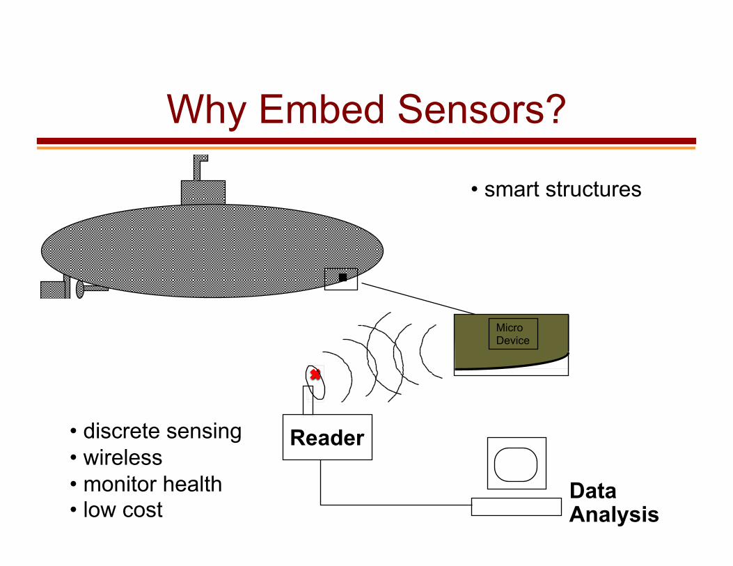
Why Embed Sensors?
• smart structures
• discrete sensing • wireless • monitor health • low cost
The image cannot be displayed. Your computer may not have enough memory to open the image, or the image may have been corrupted. Restart your computer, and then open the file again. If the red x still appears, you may have to delete the image and then insert it again.
Reader
Data Analysis
Micro Device
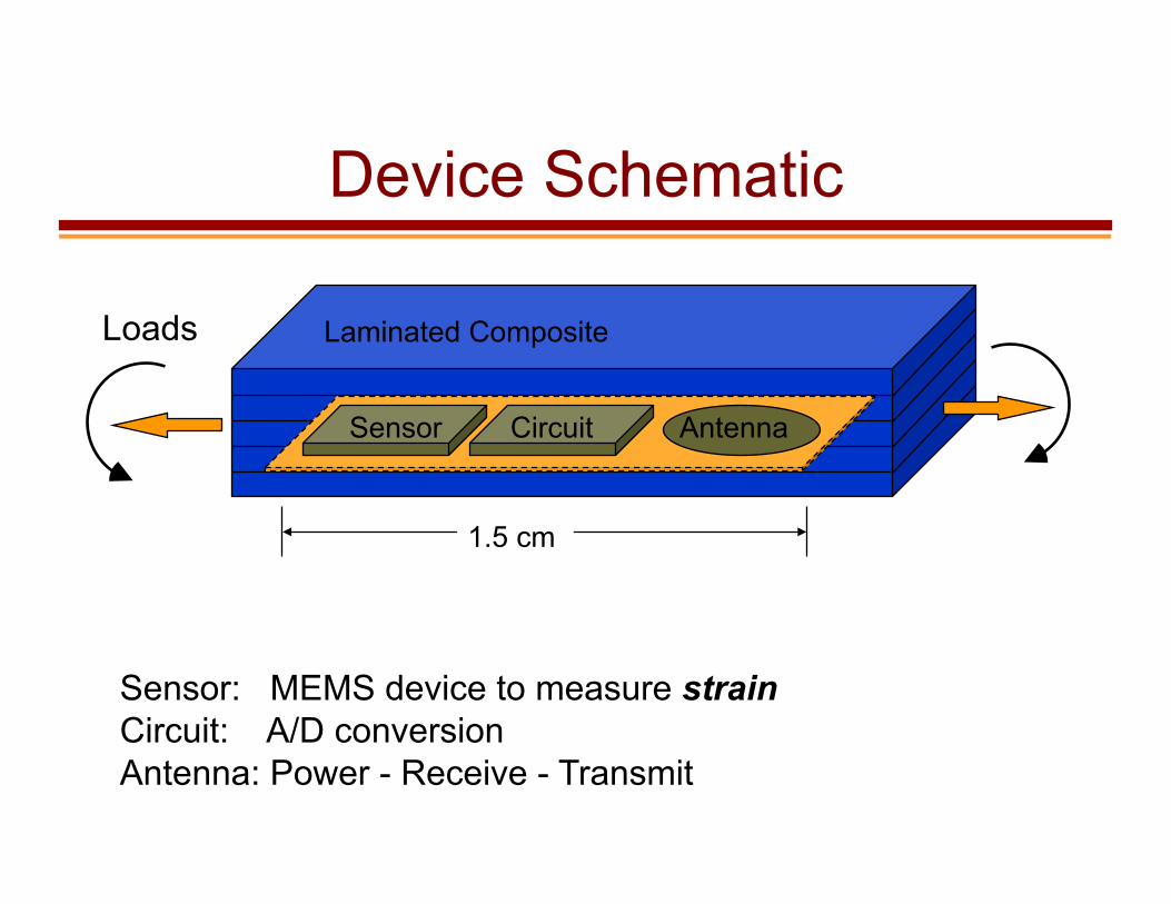
Device Schematic
1.5 cm
Laminated Composite
Sensor Circuit Antenna
Sensor: MEMS device to measure strain Circuit: A/D conversion Antenna: Power - Receive - Transmit
Loads
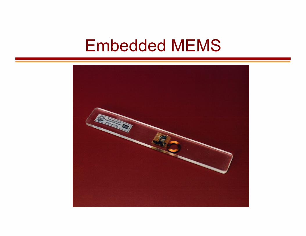
Embedded MEMS
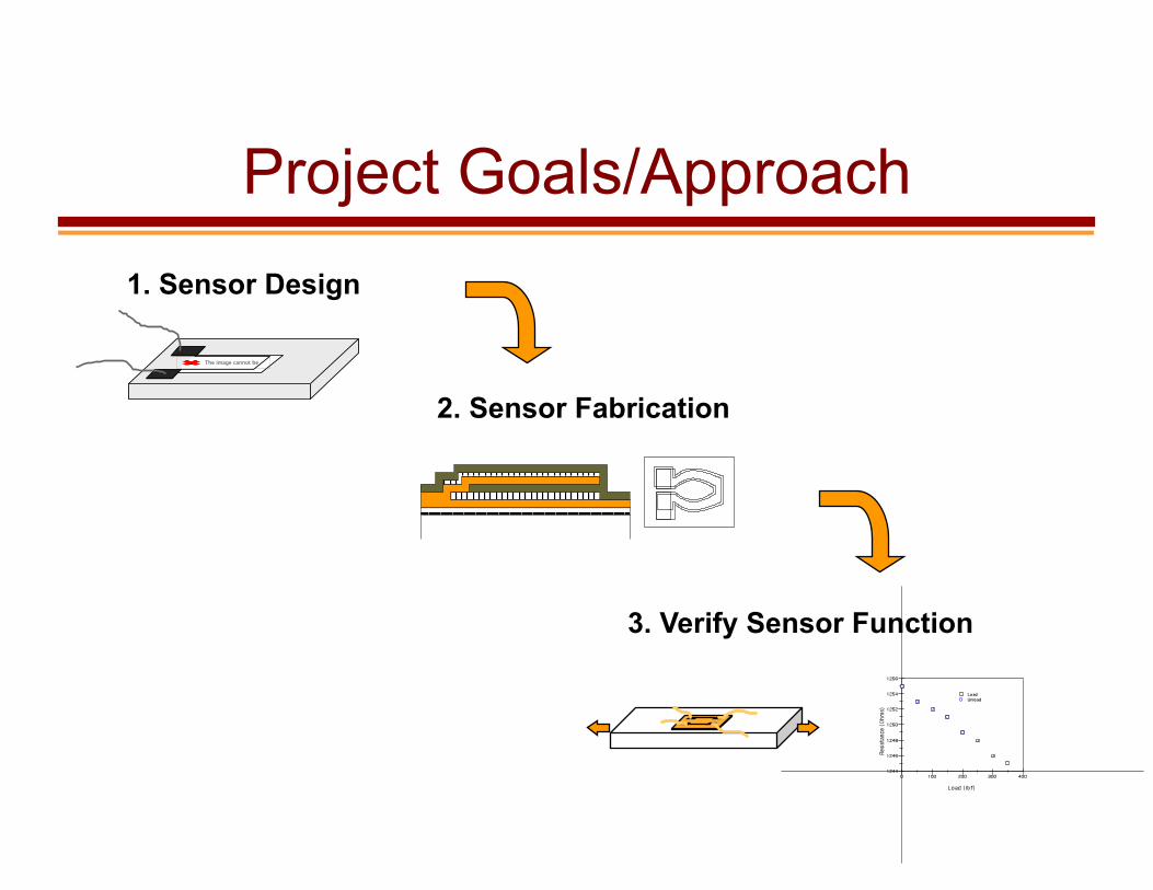
Project Goals/Approach
2. Sensor Fabrication
3. Verify Sensor Function
1. Sensor Design
The image cannot be The image cannot be
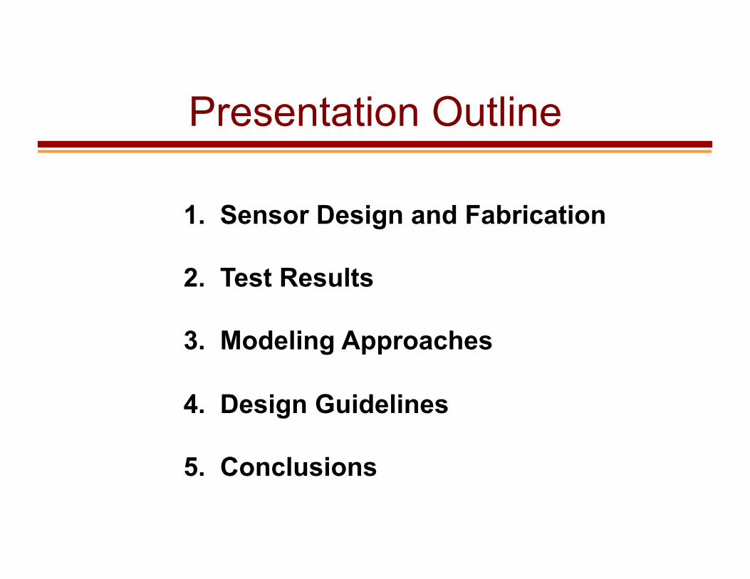
Presentation Outline
1. Sensor Design and Fabrication
2. Test Results
3. Modeling Approaches
4. Design Guidelines
5. Conclusions
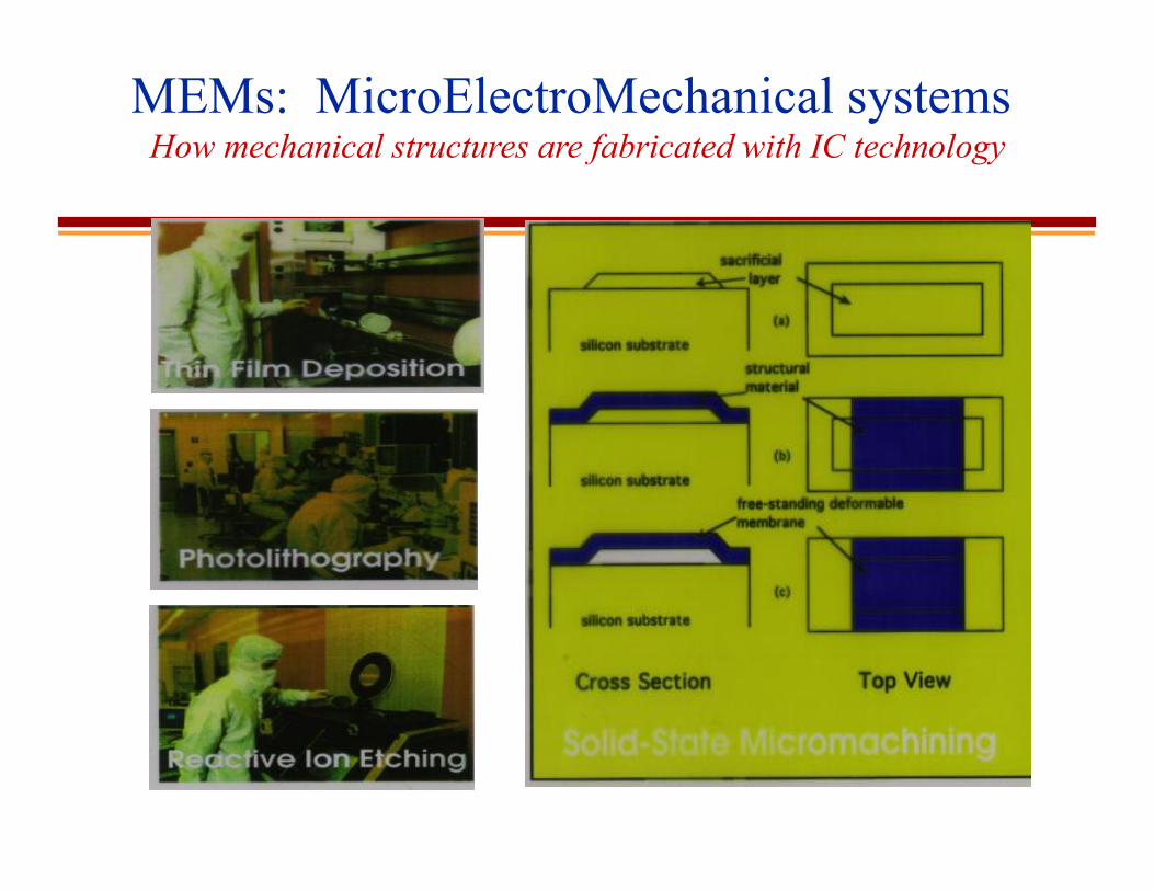
MEMs: MicroElectroMechanical systems How mechanical structures are fabricated with IC technology
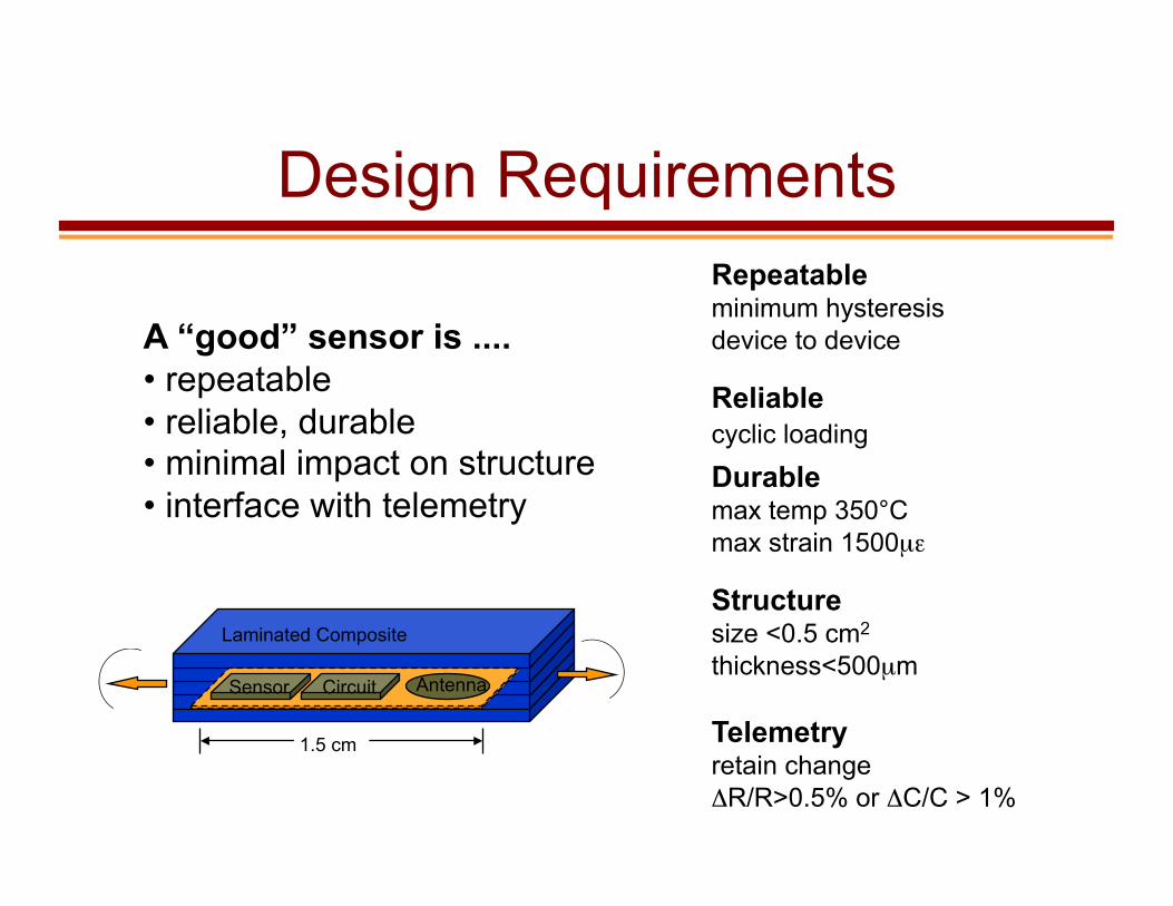
Design Requirements
A “good” sensor is .... • repeatable • reliable, durable • minimal impact on structure • interface with telemetry
Repeatable minimum hysteresis device to device
Reliable cyclic loading Durable max temp 350°C max strain 1500µε
Telemetry retain change ΔR/R>0.5% or ΔC/C > 1%
Structure size <0.5 cm2
thickness<500µm
1.5 cm
Laminated Composite
Sensor Circuit Antenna
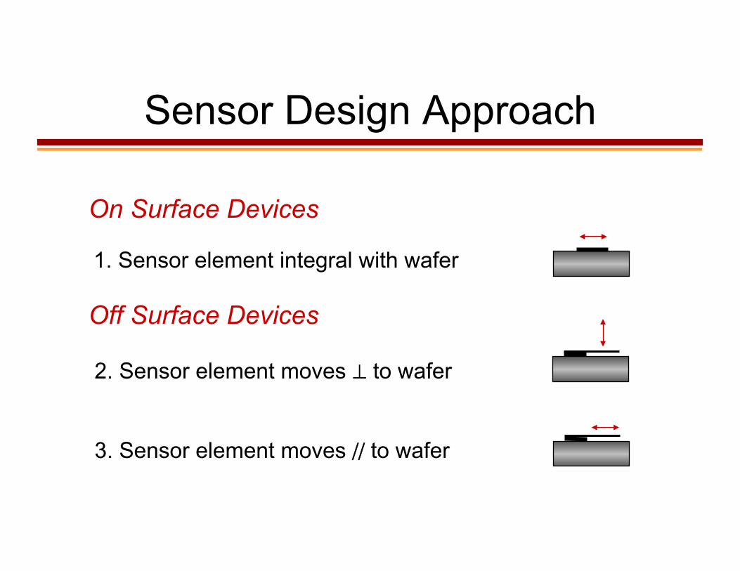
Sensor Design Approach
On Surface Devices
1. Sensor element integral with wafer
Off Surface Devices
2. Sensor element moves ⊥ to wafer
3. Sensor element moves // to wafer
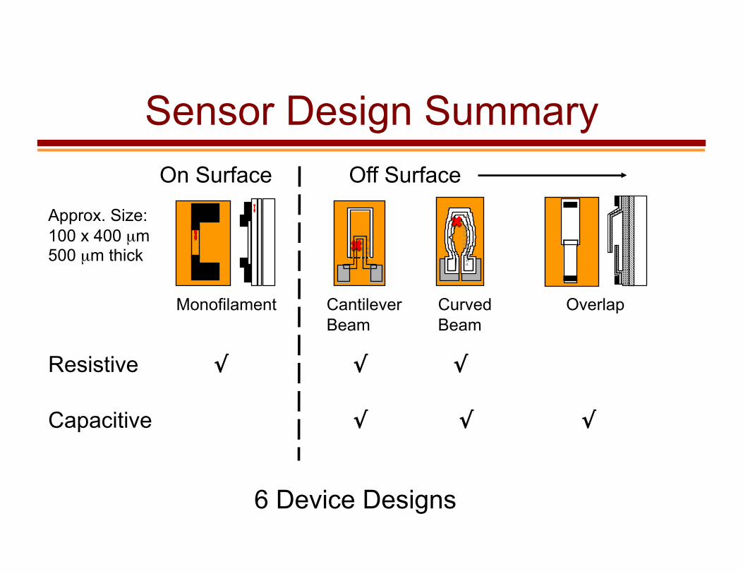
Sensor Design Summary
The image cannot be displayed. Your computer may not have enough memory to open the image, or the image may have been corrupted. Restart your computer, and then open the file again. If the red x still appears, you may have to delete the image and then insert it again.
The image cannot be displayed. Your computer may not have enough memory to open the image, or the image may have been corrupted. Restart your computer, and then open the file again. If the red x still appears, you may have to delete the image and then insert it again.
The image cann
The image cann
The image cannot be displayed. Your computer may not have enough memory to open the image, or the image may have been corrupted. Restart your computer, and then open the file again. If the red x still appears, you may have to delete the image and then insert it again.
The image cannot be displayed. Your computer may not have enough memo
The image cannot be displayed.
The image cannot be displayed.
The image cannot be displayed. Your computer may not have enough memory to open the image, or the image may have been corrupted. Restart your computer, and then open the file again. If the red x still appears, you may have to delete the image and then insert it again.
Resistive
Capacitive
On Surface Off Surface
Monofilament Cantilever Beam
Curved Beam
Overlap
√ √ √
√ √ √
Approx. Size: 100 x 400 µm 500 µm thick
6 Device Designs
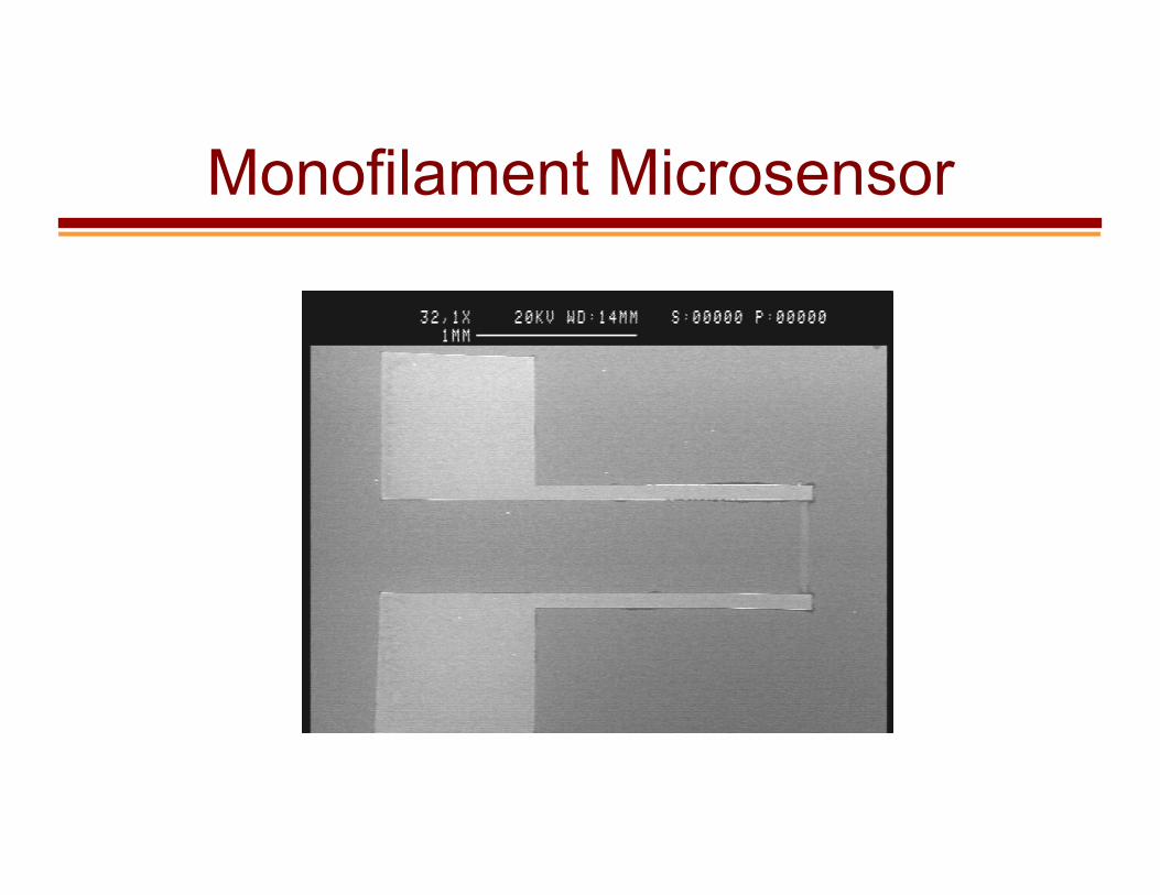
Monofilament Microsensor
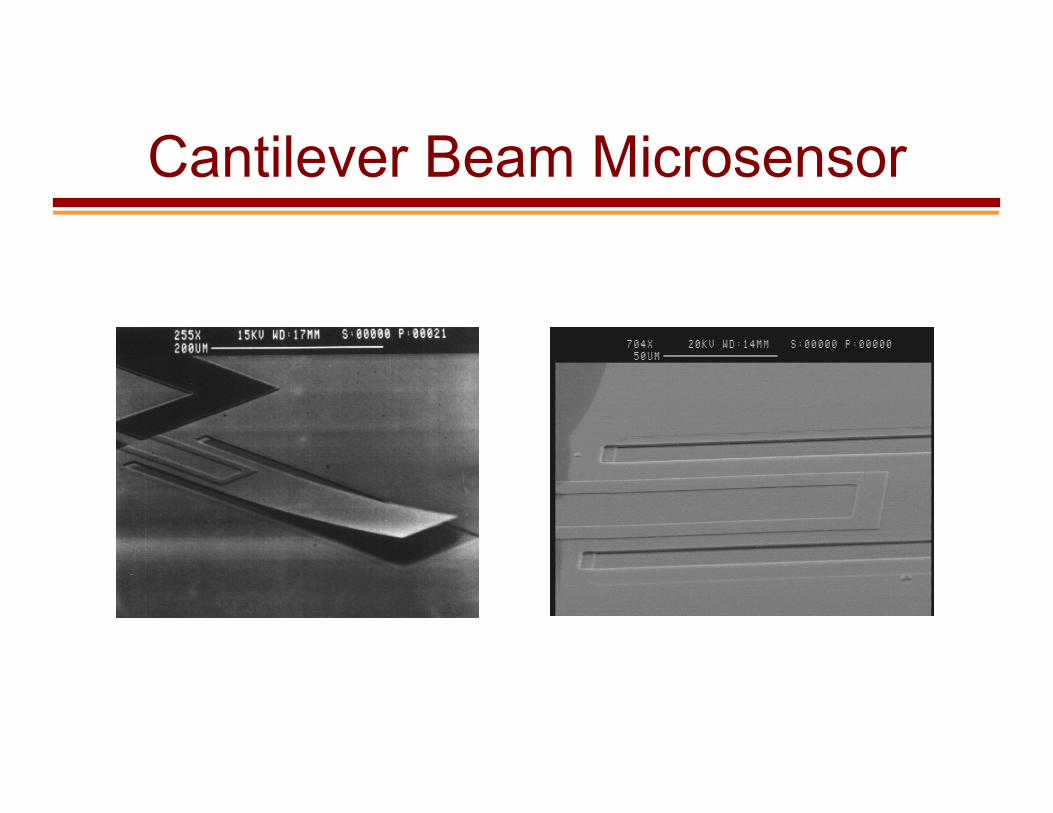
Cantilever Beam Microsensor
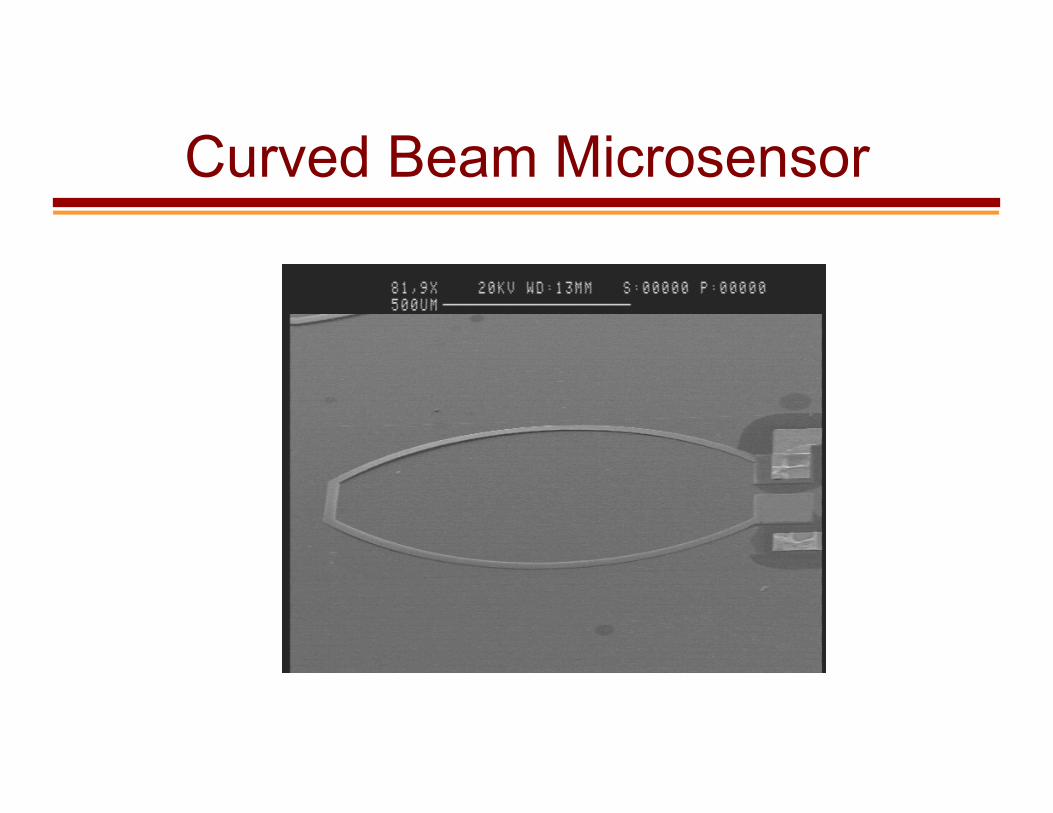
Curved Beam Microsensor
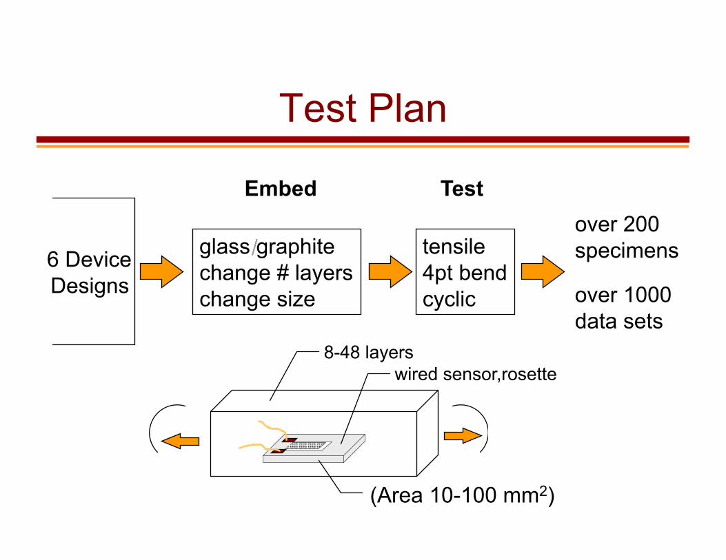
Test Plan
6 Device Designs
Embed Test
tensile 4pt bend cyclic
over 200 specimens
over 1000 data sets
(Area 10-100 mm2)
8-48 layers wired sensor,rosette
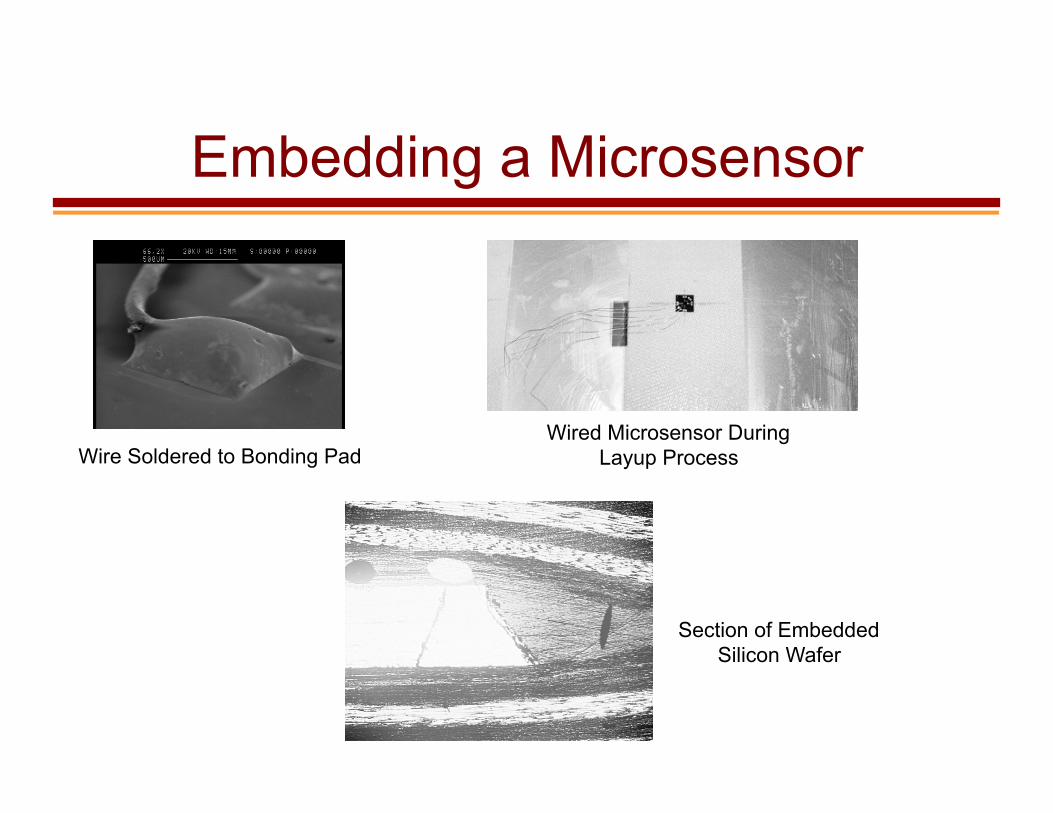
Embedding a Microsensor
Wire Soldered to Bonding Pad Wired Microsensor During
Layup Process
Section of Embedded Silicon Wafer

Mechanical Testing
Tensile Test Bending Test
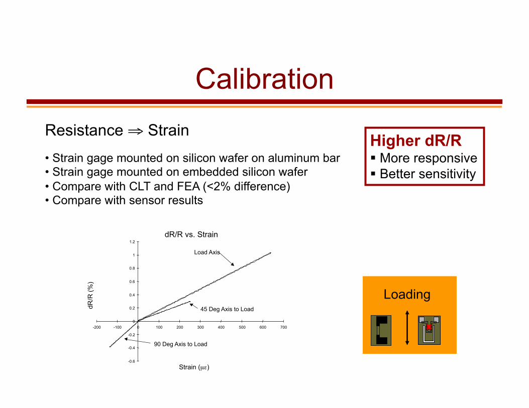
Calibration Resistance ⇒ Strain
• Strain gage mounted on silicon wafer on aluminum bar • Strain gage mounted on embedded silicon wafer • Compare with CLT and FEA (<2% difference) • Compare with sensor results
The image cannot be displayed. Your computer
The image cannot be displayed.
Loading
dR/R vs. Strain
-0.6 -0.4 -0.2
0 0.2 0.4 0.6 0.8
1 1.2
-200 -100 0 100 200 300 400 500 600 700
Strain (µε)
dR/R
(%)
Load Axis
45 Deg Axis to Load
90 Deg Axis to Load
Higher dR/R More responsive Better sensitivity
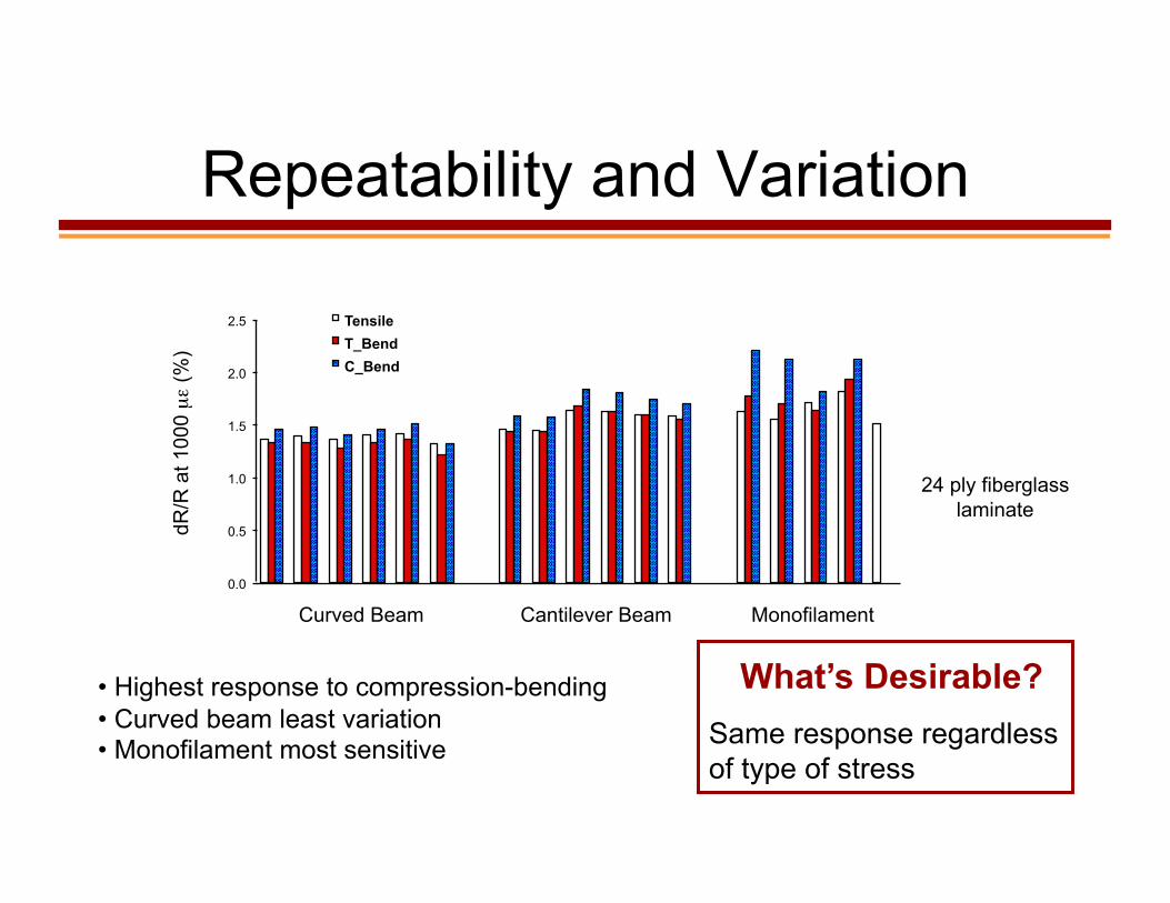
Repeatability and Variation
0.0!
0.5!
1.0!
1.5!
2.0!
2.5!
Curved Beam Cantilever Beam Monofilament!
dR/R
at 1
000
µε
(%)!
Tensile T_Bend!C_Bend!
• Highest response to compression-bending • Curved beam least variation • Monofilament most sensitive
24 ply fiberglass laminate
What’s Desirable? Same response regardless of type of stress
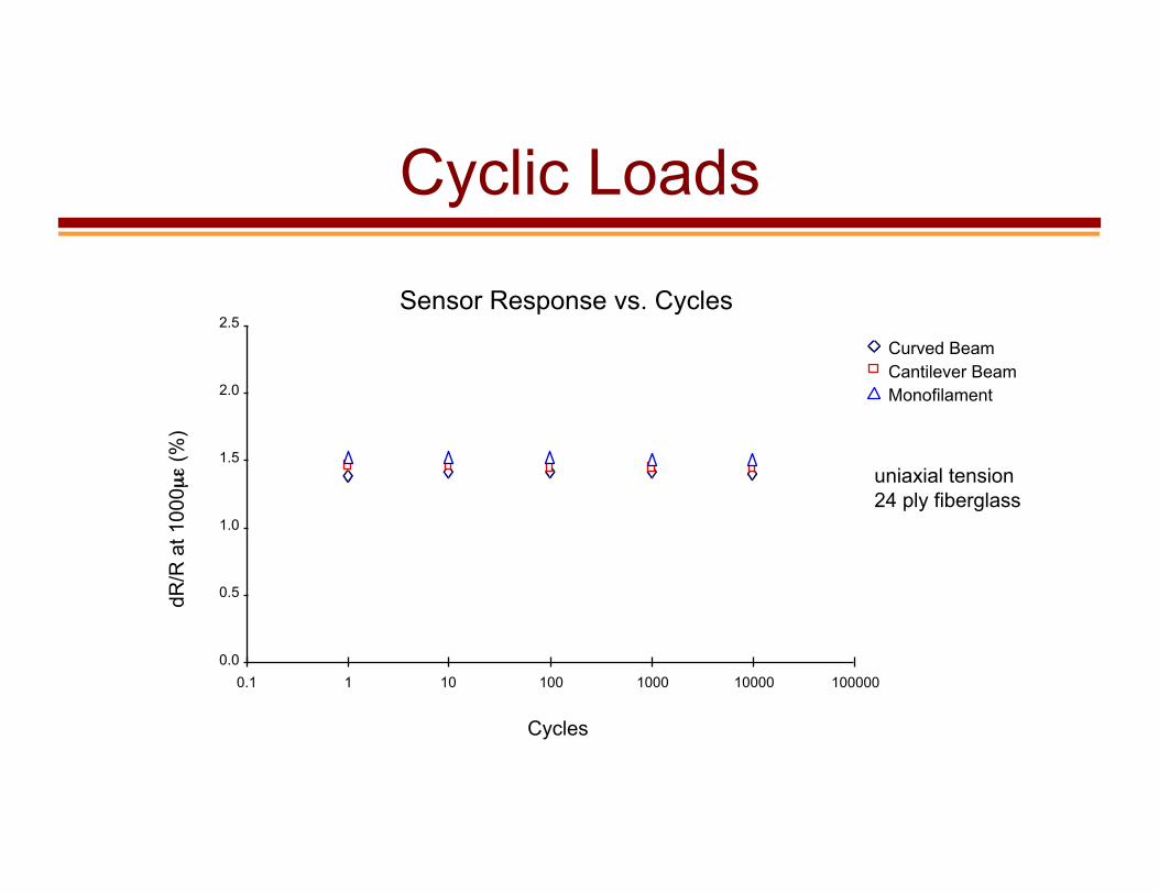
Cyclic Loads
100000 0.0!
0.5!
1.0!
1.5!
2.0!
2.5!
0.1 1 10 100 1000 10000
Cycles!
dR/R
at 1
000µε
(%)!
Curved Beam! Cantilever Beam! Monofilament
uniaxial tension 24 ply fiberglass
Sensor Response vs. Cycles

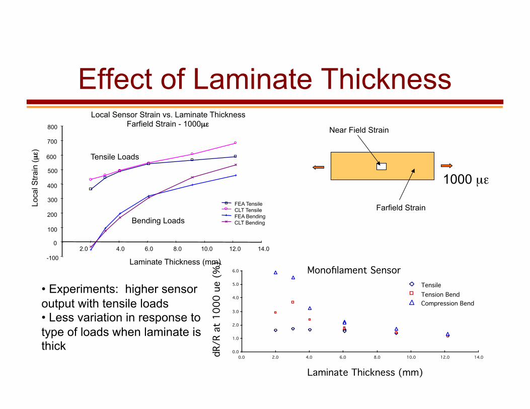
Effect of Laminate Thickness
Curved Beam Sensor!
0.0!
1.0!
2.0!
3.0!
4.0!
5.0!
6.0!
0.0! 2.0! 4.0! 6.0! 8.0! 10.0! 12.0! 14.0!
Laminate Thickness (mm)
dR/R
at 1
000µε
(%)! Tensile
Tension Bend Compression Bend
Monofilament Sensor!
0.0!
1.0!
2.0
3.0!
4.0!
5.0!
6.0!
0.0! 2.0 4.0 6.0 8.0! 10.0! 12.0! 14.0!
Laminate Thickness (mm)
dR/R
at 1
000µε
(%)!
Tensile Tension Bend Compression Bend
• Silicon wafer affects sensor response to bending
• Local bending of wafer dominates sensor response for thin laminates
• Off surface shows more consistent performance for thin laminates
On surface vs. Off surface
Performance depends on loading
ΔR/R should not be f(loading, laminate thickness)

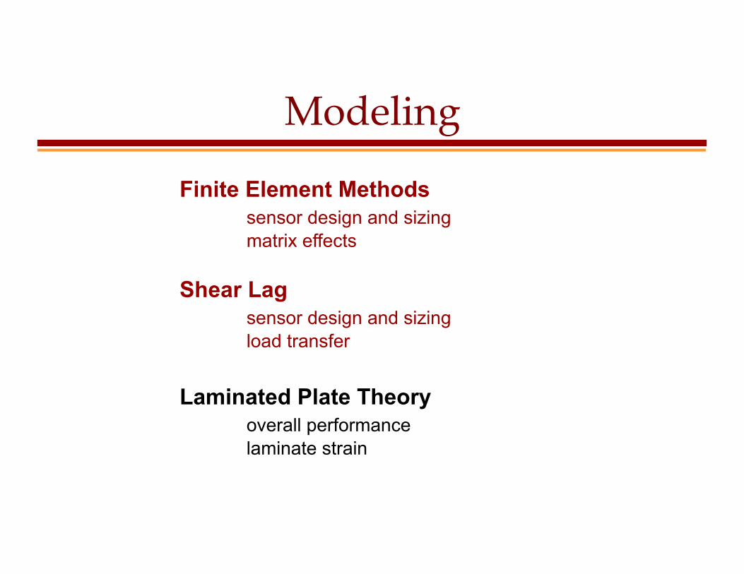
Modeling
Laminated Plate Theory overall performance laminate strain
Finite Element Methods sensor design and sizing matrix effects
Shear Lag sensor design and sizing load transfer
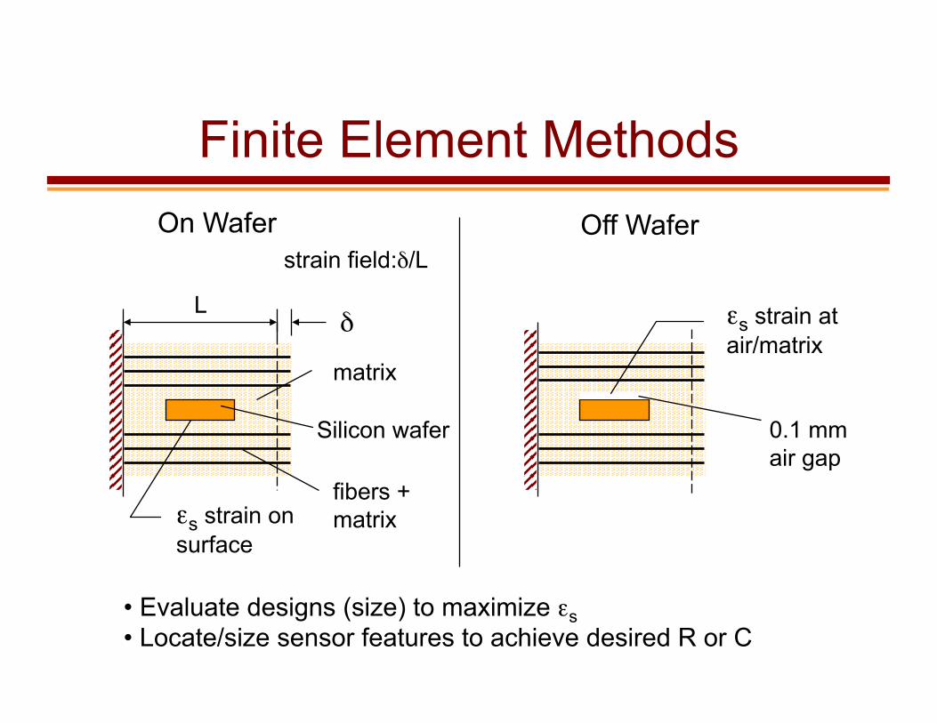
Finite Element Methods On Wafer Off Wafer
εs strain on surface
L δ
fibers + matrix
Silicon wafer
strain field:δ/L
matrix
0.1 mm air gap
εs strain at air/matrix
• Evaluate designs (size) to maximize εs • Locate/size sensor features to achieve desired R or C
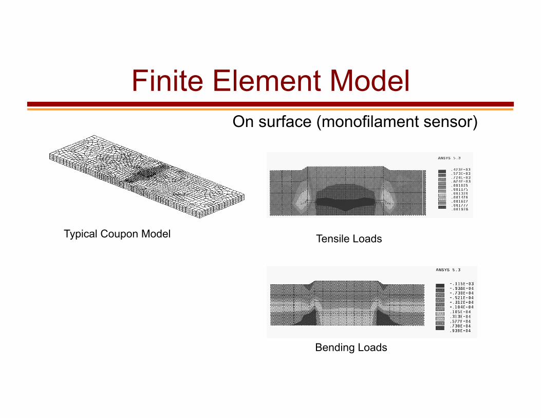
Finite Element Model
Typical Coupon Model Tensile Loads
Bending Loads
On surface (monofilament sensor)
Finite Element Model
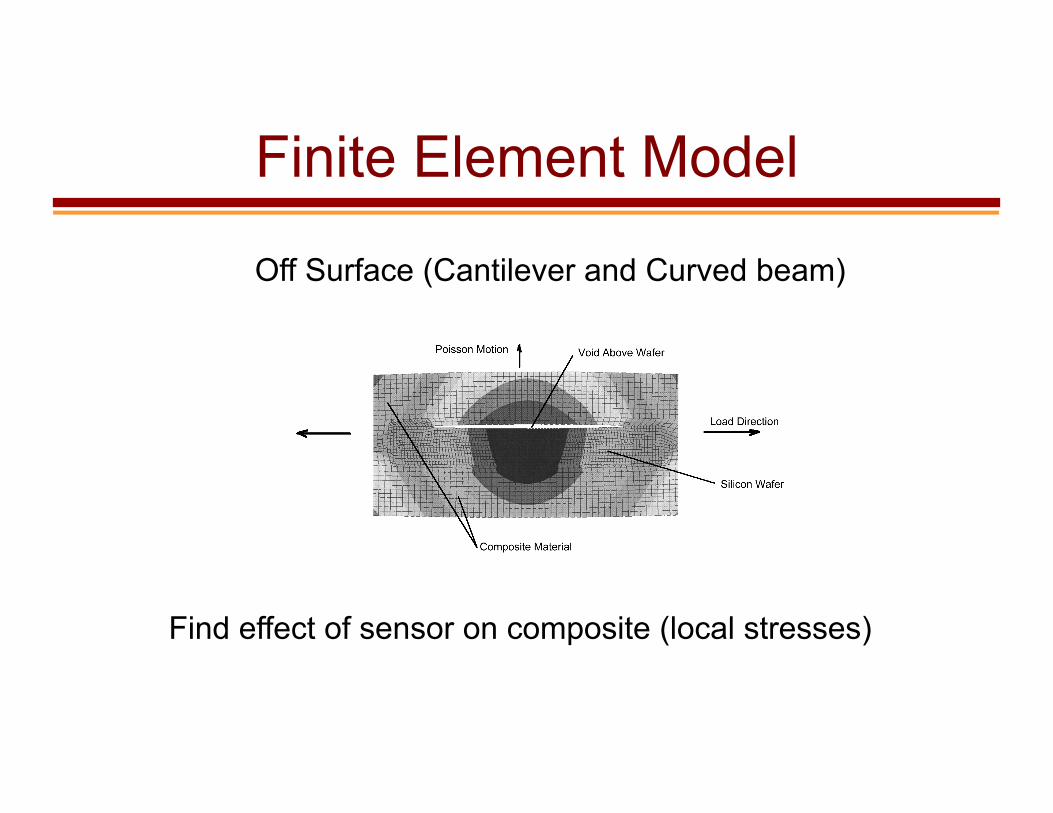
Off Surface (Cantilever and Curved beam)
Find effect of sensor on composite (local stresses)
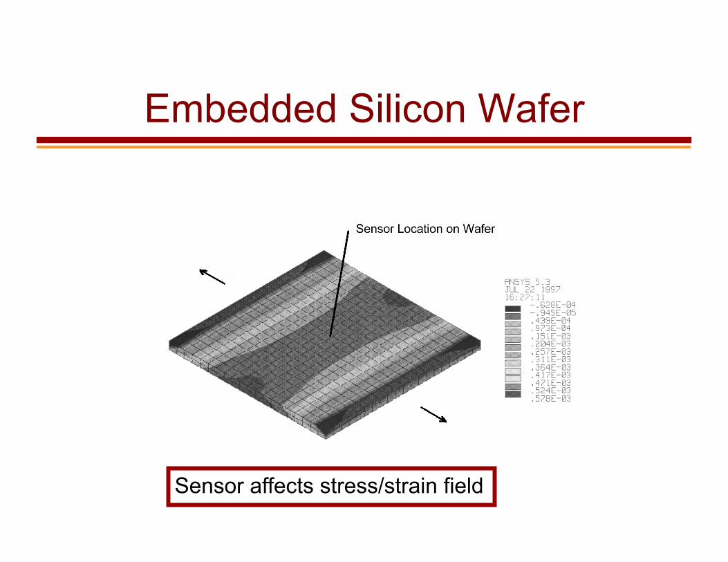
Embedded Silicon Wafer
Sensor affects stress/strain field
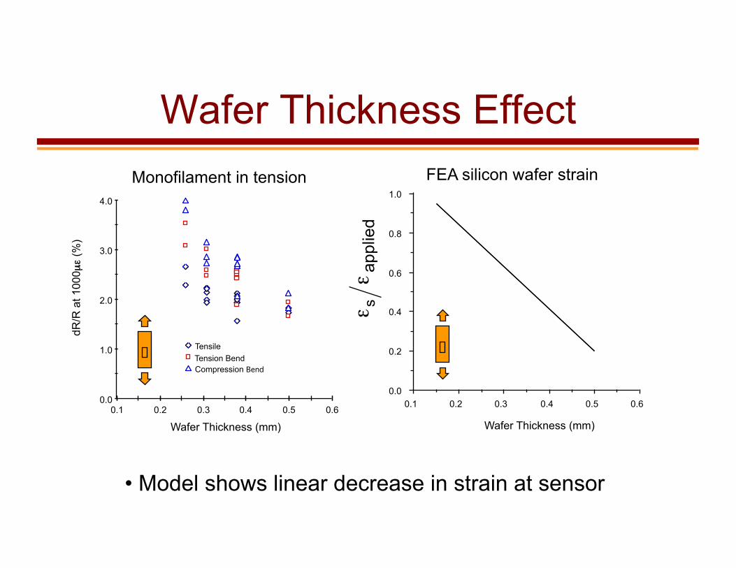
Wafer Thickness Effect
Wafer Thickness (mm)
Monofilament in tension FEA silicon wafer strain
• Model shows linear decrease in strain at sensor
0.6!0.5!0.4!0.3!0.2!0.1!0.0!
0.2!
0.4!
0.6!
0.8!
1.0!
ε s ε ap
plie
d 0.0!
1.0!
2.0!
3.0!
4.0!
0.1! 0.2! 0.3! 0.4! 0.5! 0.6!
Wafer Thickness (mm)
dR/R
at 1
000µε
(%)!
Tensile! Tension Bend Compression Bend!
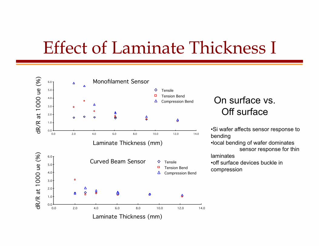
Effect of Laminate Thickness I
Curved Beam Sensor!
0.0!
1.0!
2.0!
3.0!
4.0!
5.0!
6.0!
0.0! 2.0! 4.0! 6.0! 8.0! 10.0! 12.0! 14.0!
Laminate Thickness (mm)!
dR/R
at
1000
ue
(%)!
Tensile!Tension Bend!Compression Bend!
Monofilament Sensor!
0.0!
1.0!
2.0!
3.0!
4.0!
5.0!
6.0!
0.0! 2.0! 4.0! 6.0! 8.0! 10.0! 12.0! 14.0!
Laminate Thickness (mm)!
dR/R
at
1000
ue
(%)!
Tensile!Tension Bend!Compression Bend!
• Si wafer affects sensor response to bending • local bending of wafer dominates
sensor response for thin laminates • off surface devices buckle in compression
On surface vs. Off surface
Effect of Laminate Thickness
• Experiments: higher sensor output with tensile loads • Less variation in response to type of loads when laminate is thick
Local Sensor Strain vs. Laminate Thickness Farfield Strain - 1000µε
-100 0
100 200 300 400 500 600 700 800
2.0 4.0 6.0 8.0 10.0 12.0 14.0 Laminate Thickness (mm)
Loca
l Stra
in (µε)
FEA Tensile CLT Tensile FEA Bending CLT Bending
Tensile Loads
Bending Loads Farfield Strain
Near Field Strain
Monofilament Sensor!
0.0!
1.0!
2.0!
3.0!
4.0!
5.0!
6.0!
0.0! 2.0! 4.0! 6.0! 8.0! 10.0! 12.0! 14.0!
Laminate Thickness (mm)!
dR/R
at
1000
ue
(%)!
Tensile!Tension Bend!Compression Bend!
1000 µε
Modeling
Laminated Plate Theory overall performance laminate strain
Finite Element Methods sensor design and sizing matrix effects
Shear Lag sensor design and sizing load transfer

Effects of Wafer Geometry
• From Shear lag theory GF = [(w + t)/(w * t )] * L
Off Surface Sensors!
0.0!
1.0!
2.0!
3.0!
4.0!
10.0! 11.0 12.0! 13.0! 14.0! 15.0
Geometry Factor!
dR/R
at 1
000µε
(%)!
CB Cantilever
T Cantilever TB Cantilever
T Curved TB Curved CB Curved
Monofilament Sensor!
0.0!
1.0!
2.0!
3.0!
4.0!
0.0! 5.0! 10.0! 15.0! 20.0! 25.0! 30.0!
Geometry Factor!
dR/R
at 1
000µε
(%)!
Tensile Tension Bend Compression Bend!
•
Off Surface Sensors Wafer geometry has no effect
On Surface Sensors Higher GF improves response

Sensor Design Summary
The image cannot be displayed. Your computer may not have enough memory to open the image, or the image may have been corrupted. Restart your computer, and then open the
On Surface
Monofilament
The image cannot be displayed. Your computer may not have enough memory to open the image, or the image may have been corrupted. Restart your computer,
The image cannot be displayed. Your computer may not have enough memory to open the image, or the image may have been corrupted. Restart
The image cannot be displa
Off Surface
Cantilever Beam
Curved Beam
• Thinned difficult to fabricate • Large device to device variation • Large variation in ΔR/R from tension to bending • Best ΔR/R • Ability to detect Poisson's effect
• Small device to device variation • Consistent ΔR/R from tension to bending • Adequate ΔR/R

Completed Strain MEMS
Sensor

Conclusions
Accomplishments • Designed, fabricated and tested MEMS strain sensors • Demonstrated that MEMS can measure strain • Developed modeling tools for sensor, and sensor/composite
Strain Sensor Design Guides • Thinned, or off wafer devices for best strain transfer • Off wafer designs respond consistently to loads • On surface design detects Poisson's effect • Piezoresistive material, maintains change,well characterized
Laminated Composite
Sensor Circuit Antenna

Performance in Liquids


Laminated Plate Theory µε
400!300!200!100!0!0!
1000!
2000!measured, sensor!calculated LPT!
Load (lbf)!
Stra
in!
sensor: thinned (150 µm) monofilament load: tension
• calibrated (R->ε) from residual strain data
• LPT indicates effect of sensor on strain field
• thinned sensor has minimal effect on local strains

Proposed Flexible Microsensor
Silicon Wafer
Electronics Polyimide Layer Polysilicon Sensor

Multi-beam Capacitive Sensors

Sensor Repeatability
400!300 200!100 0!1244!
1246!
1248!
1250!
1252!
1254!
1256!load unload
Load (lbf)
Res
ista
nce
(Ohm
s)!
Monofilament Sensor
1200 1000!800!600!400!200!0!715!
720!
725
Load (lbf)
Res
ista
nce
(ohm
s)!
specimen 1!
specimen 2!
load unload
Cantilever Beam Sensor
The ima
Tensile Test

Silicon Wafer on Aluminum Bar

Variation among Devices Tension
0.26
mon
o!
0.50
mon
o!
cant
bea
m!
curv
ed b
eam!
stra
in g
age!
0.0!
0.2!
0.4!
0.6!
0.8!
1.0!
1.2!
1.4!
0.0!
0.2!
0.4!
0.6!
0.8!
1.0!
1.2!
1.4!
0.26
mon
o!
0.50
mon
o!
cant
bea
m!
curv
ed b
eam!
stra
in g
age!
Bending improved response in bending
R/R
at 1
000
Δ
µε
on wafer off wafer on wafer off wafer

Geometry Factor Derivation
w t
L
dx τ
σ w + d σ w
σ w
Wafer
GF = [(w + t)/(w * t )] * L


