
EECS 142
Lecture 23: Negative Resistance Osc, Differential Osc,and VCOs
Prof. Ali M. Niknejad
University of California, Berkeley
Copyright c© 2005 by Ali M. Niknejad
A. M. Niknejad University of California, Berkeley EECS 142 Lecture 23 p. 1/28 – p. 1/28
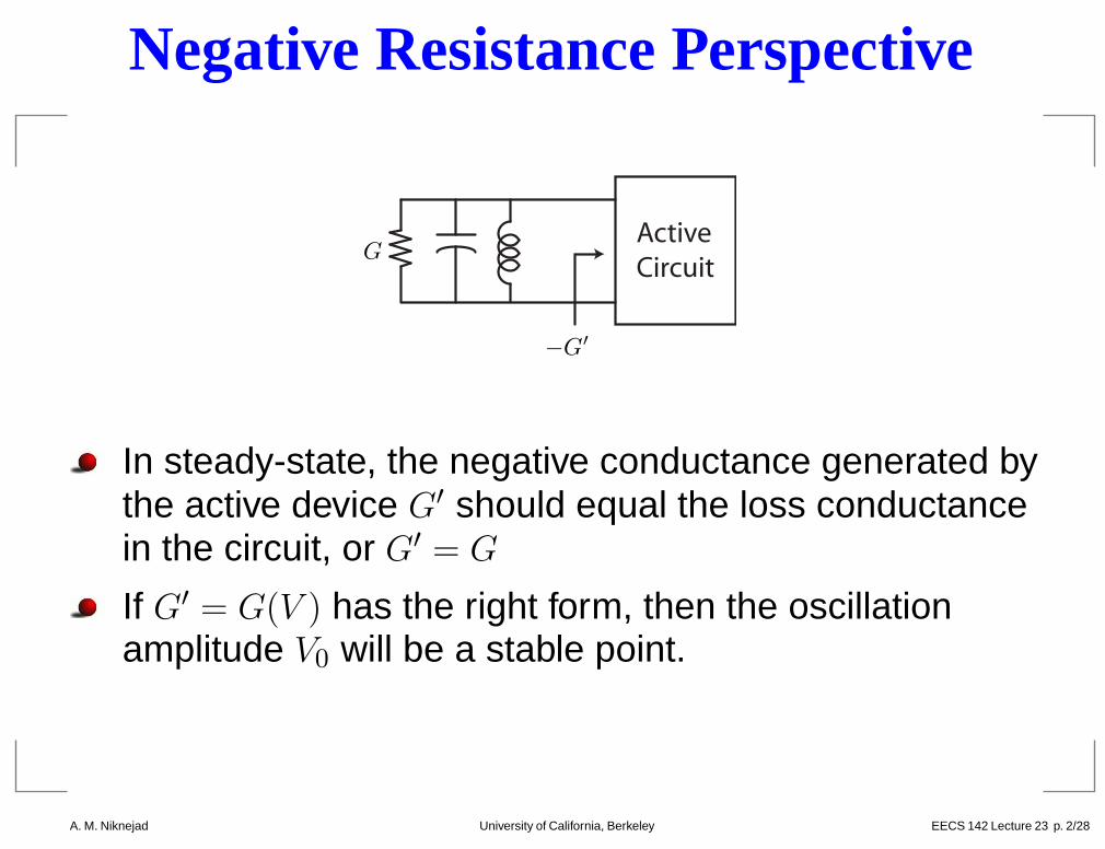
Negative Resistance Perspective
Active
Circuit
′
G
−G
In steady-state, the negative conductance generated bythe active device G′ should equal the loss conductancein the circuit, or G′ = G
If G′ = G(V ) has the right form, then the oscillationamplitude V0 will be a stable point.
A. M. Niknejad University of California, Berkeley EECS 142 Lecture 23 p. 2/28 – p. 2/28

Oscillator Stability (Intuition)
G′
V0
V
G(V )
Intuitively we can see that if the amplitude grows aboveV0 by δV , then G′ < G and the circuit has net loss. Theoscillation amplitude will thus decrease.
Likewise, if the amplitude drops by some increment δV ,then G′ > G and net energy is added to the circuit oneach cycle. The oscillation amplitude will thereforegrow.
A. M. Niknejad University of California, Berkeley EECS 142 Lecture 23 p. 3/28 – p. 3/28
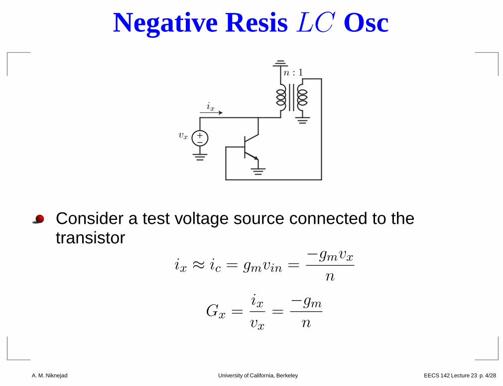
Negative Resis LC Osc
vx
ix
n : 1
+
Consider a test voltage source connected to thetransistor
ix ≈ ic = gmvin =gmvxn
Gx =ixvx
=gmn
A. M. Niknejad University of California, Berkeley EECS 142 Lecture 23 p. 4/28 – p. 4/28
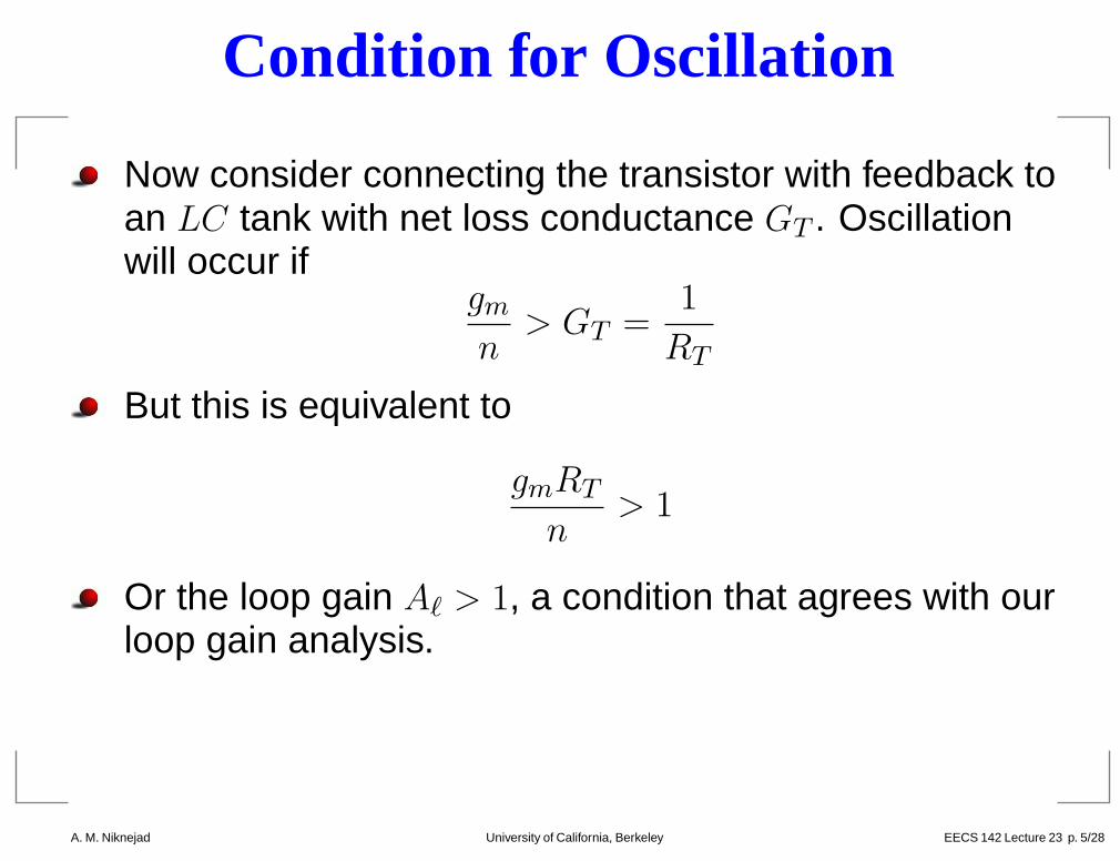
Condition for Oscillation
Now consider connecting the transistor with feedback toan LC tank with net loss conductance GT . Oscillationwill occur if
gmn
> GT =1
RT
But this is equivalent to
gmRT
n> 1
Or the loop gain Aℓ > 1, a condition that agrees with ourloop gain analysis.
A. M. Niknejad University of California, Berkeley EECS 142 Lecture 23 p. 5/28 – p. 5/28

Colpitts Osc
vx
ix
C1
C2
Connect a test current source as before. PerformingKCL
ix = gmv1 + (vx v1)jωC1
v1jωC ′
2 + (v1 vx)jωC1 + v1gπ + gmv1 = 0
Where C ′
2= C2 + Cπ. Notice that Cµ can be absorbed
into the tank.
A. M. Niknejad University of California, Berkeley EECS 142 Lecture 23 p. 6/28 – p. 6/28

Colpitts (cont)
Simplifying, we see that
v1
vx=
jωC1
jω(C1 + C ′
2) + gm + gπ
≈C1
C1 + C ′
2
=1
n
The above result follows directly from the capacitordivider. But notice that the assumption only holds whenthe capacitive susceptance dominates over thetransistor transconductance.
Using the above result we have
Gx =ixvx
=gmn
+ jωC1C
′
2
C1 + C ′
2
A. M. Niknejad University of California, Berkeley EECS 142 Lecture 23 p. 7/28 – p. 7/28
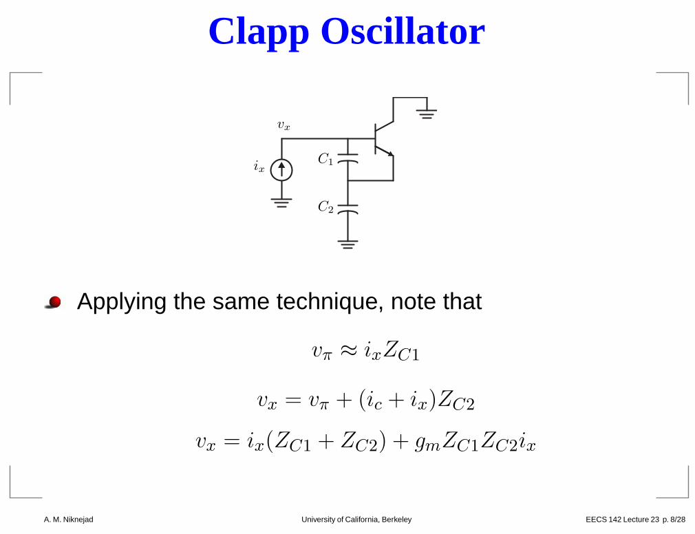
Clapp Oscillator
vx
ixC1
C2
Applying the same technique, note that
vπ ≈ ixZC1
vx = vπ + (ic + ix)ZC2
vx = ix(ZC1 + ZC2) + gmZC1ZC2ix
A. M. Niknejad University of California, Berkeley EECS 142 Lecture 23 p. 8/28 – p. 8/28

Clapp (cont)
The input impedance seen by the source is given by
Zx =vxix
=1
jωC1
+1
jωC2
+gm
jωC1jωC2
The negative resistance of the Clapp depends onfrequency
Rx = ℜ(Zx) =gm
ω2C1C2
Oscillation will occur if the negative resistancegenerated by the transistor is larger than the series lossin the tank
|Rx| > Rs
gm > Rsω2C1C2
A. M. Niknejad University of California, Berkeley EECS 142 Lecture 23 p. 9/28 – p. 9/28
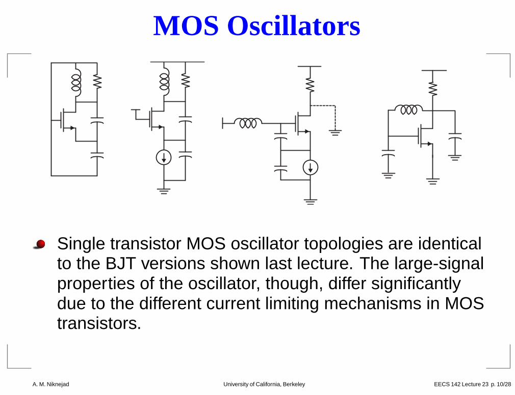
MOS Oscillators
Single transistor MOS oscillator topologies are identicalto the BJT versions shown last lecture. The large-signalproperties of the oscillator, though, differ significantlydue to the different current limiting mechanisms in MOStransistors.
A. M. Niknejad University of California, Berkeley EECS 142 Lecture 23 p. 10/28 – p
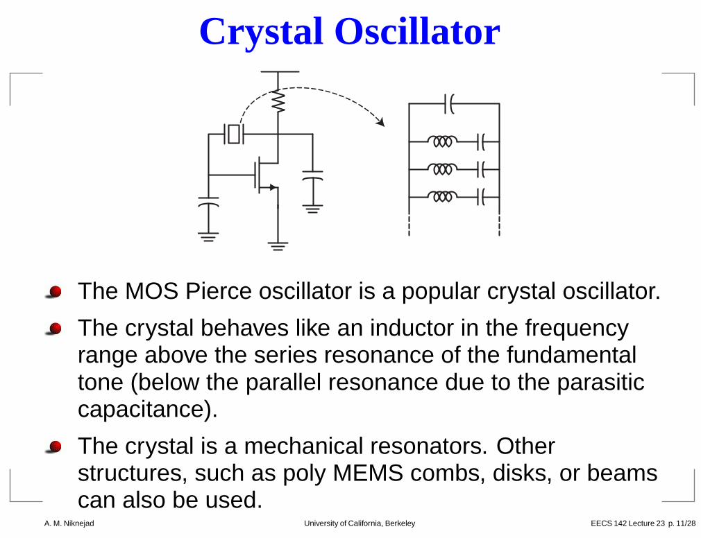
Crystal Oscillator
The MOS Pierce oscillator is a popular crystal oscillator.
The crystal behaves like an inductor in the frequencyrange above the series resonance of the fundamentaltone (below the parallel resonance due to the parasiticcapacitance).
The crystal is a mechanical resonators. Otherstructures, such as poly MEMS combs, disks, or beamscan also be used.
A. M. Niknejad University of California, Berkeley EECS 142 Lecture 23 p. 11/28 – p
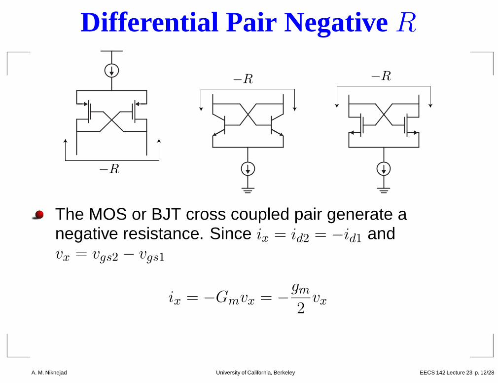
Differential Pair Negative R
−R
−R −R
The MOS or BJT cross coupled pair generate anegative resistance. Since ix = id2 = id1 andvx = vgs2 vgs1
ix = Gmvx =gm2
vx
A. M. Niknejad University of California, Berkeley EECS 142 Lecture 23 p. 12/28 – p

Cross-Coupled Resistancevx
+
ix
M1 M2
id1 id2
Gx =ixvx
=gm2
The above equivalent circuit can be used to find theimpedance of the cross-coupled pair.
At high-frequency the device capacitance and inputresistance should be included in the analysis.
A. M. Niknejad University of California, Berkeley EECS 142 Lecture 23 p. 13/28 – p

Differential Oscillator
We can connect two inductors or a single center-tappedinductor.
A center-tapped inductor consumes less area than twoseparate inductors due to the mutual inductancebetween the windings.
A. M. Niknejad University of California, Berkeley EECS 142 Lecture 23 p. 14/28 – p

BJT Differential Pair Osc
A BJT version of the oscillator has limited voltage swingdetermined by the differential pair non-linearity. We canincrease the voltage swing by emitter degeneration.
A more popular alternative is to provide feedbackcapacitors. The negative conductance is decreased bythe feedback factor.
A. M. Niknejad University of California, Berkeley EECS 142 Lecture 23 p. 15/28 – p
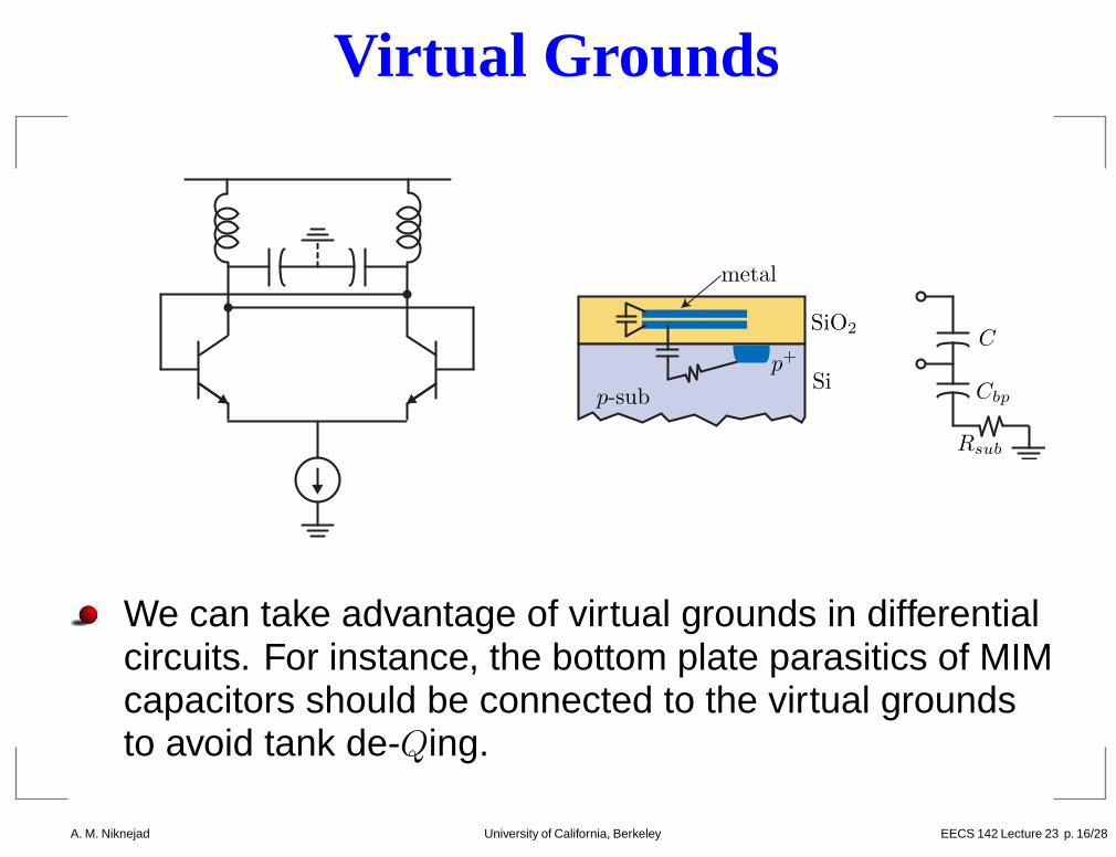
Virtual Grounds
p+
p-sub
SiO2
Si
metal
C
Cbp
Rsub
We can take advantage of virtual grounds in differentialcircuits. For instance, the bottom plate parasitics of MIMcapacitors should be connected to the virtual groundsto avoid tank de-Qing.
A. M. Niknejad University of California, Berkeley EECS 142 Lecture 23 p. 16/28 – p

MOS Variations
PMOS devices have less 1/f noise and so a PMOScurrent source will mix less power into the fundamental.
Using both PMOS and NMOS differential pairs canlower the current consumption of the oscillator
G′ = Gp + GnA. M. Niknejad University of California, Berkeley EECS 142 Lecture 23 p. 17/28 – p

Voltage-Controlled Osc
In most applications we need to tune the oscillator to aparticular frequency electronically.
A voltage controlled oscillator (VCO) has a separate“control” input where the frequency of oscillation is afunction of the control signal Vc
The tuning range of the VCO is given by the range infrequency normalized to the average frequency
TR = 2fmax fminfmax + fmin
A typical VCO might have a tuning range of 20% 30%to cover a band of frequencies (over process andtemperature)
A. M. Niknejad University of California, Berkeley EECS 142 Lecture 23 p. 18/28 – p

PN Junction Varactors
The most common way to control the frequency is byusing a reverse biased PN junction
The small signal capacitance is given by
Cj = Ajǫ
xdep=
Cj0(
1 Vj
ψ0
)n
The above formula is easily derived by observing that apositive increment in reverse bias voltage requires anincrement of growth of the depletion region width. Sincecharge must flow to the edge of the depletion region,the structure acts like a parallel plate capacitors forsmall voltage perturbations.
A. M. Niknejad University of California, Berkeley EECS 142 Lecture 23 p. 19/28 – p
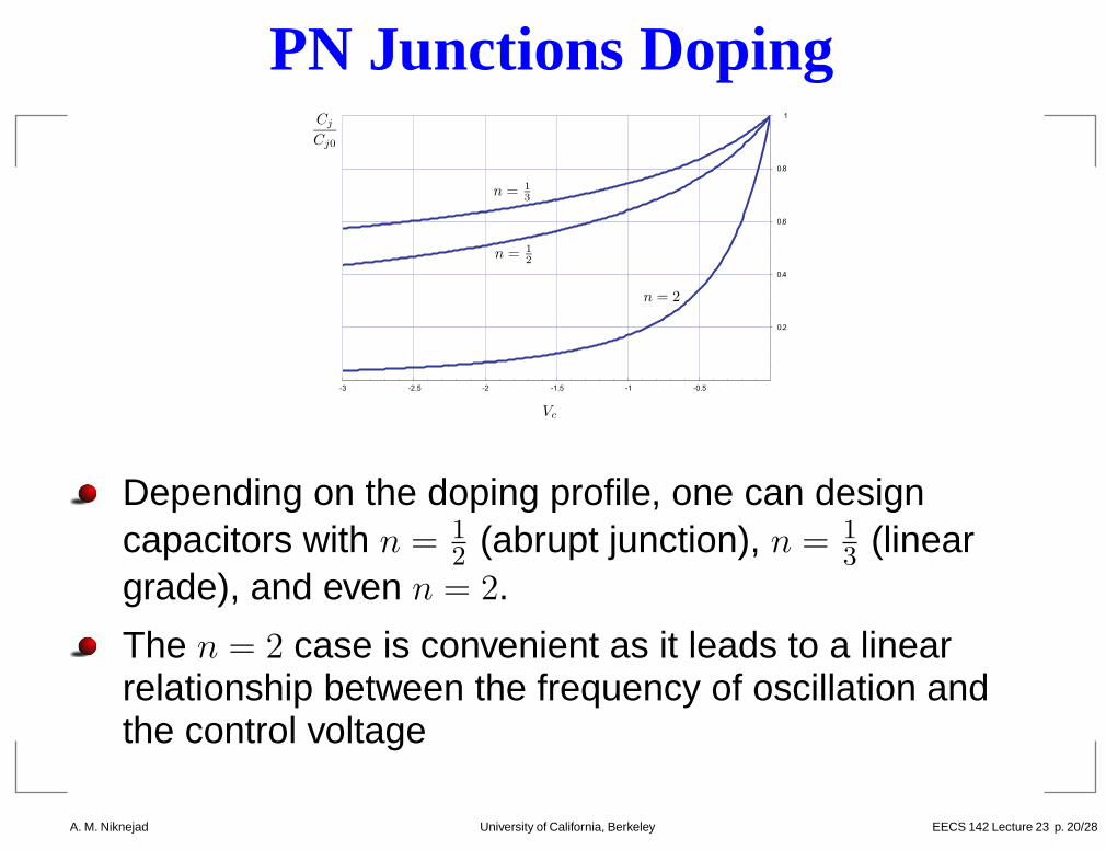
PN Junctions Doping
-3 -2.5 -2 -1.5 -1 -0.5
0.2
0.4
0.6
0.8
1
n = 1
2
n = 2
n = 1
3
Cj
Cj0
Vc
Depending on the doping profile, one can designcapacitors with n = 1
2(abrupt junction), n = 1
3(linear
grade), and even n = 2.
The n = 2 case is convenient as it leads to a linearrelationship between the frequency of oscillation andthe control voltage
A. M. Niknejad University of California, Berkeley EECS 142 Lecture 23 p. 20/28 – p
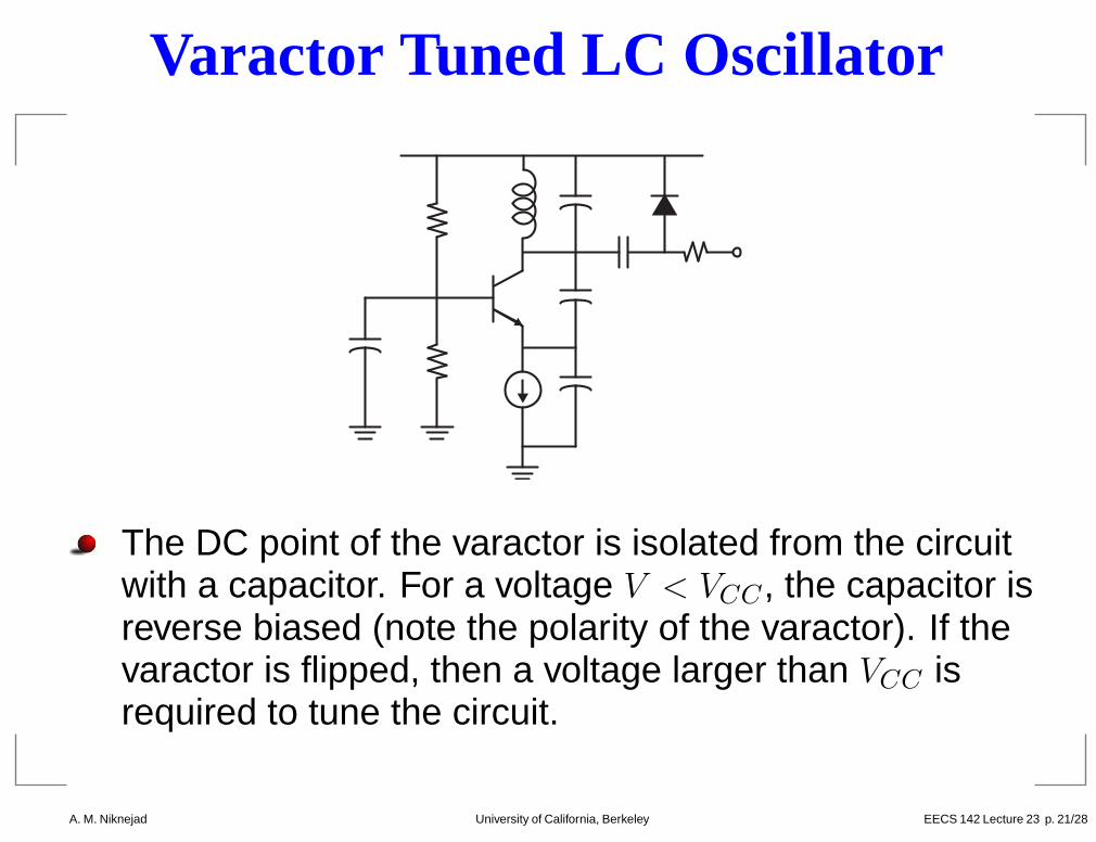
Varactor Tuned LC Oscillator
The DC point of the varactor is isolated from the circuitwith a capacitor. For a voltage V < VCC , the capacitor isreverse biased (note the polarity of the varactor). If thevaractor is flipped, then a voltage larger than VCC isrequired to tune the circuit.
A. M. Niknejad University of California, Berkeley EECS 142 Lecture 23 p. 21/28 – p

Clapp Varactor Tuned VCO
CB
C1
C2
RB
Vc
Similar to the previous case the varactor is DC isolated
In all varactor tuned VCOs, we must avoid forwardbiasing the varactor since it will de-Q the tank
A. M. Niknejad University of California, Berkeley EECS 142 Lecture 23 p. 22/28 – p
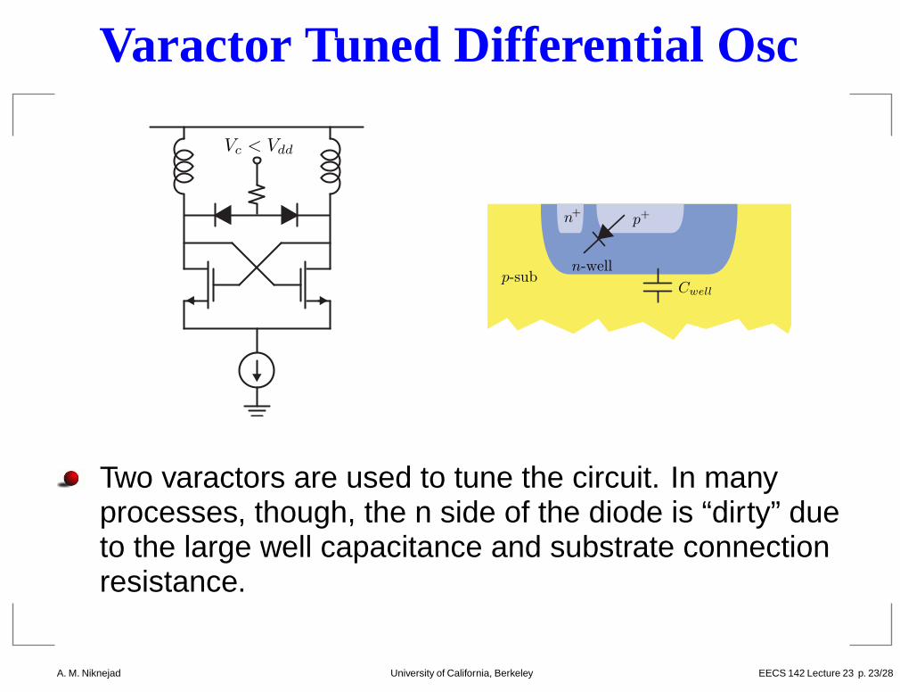
Varactor Tuned Differential Osc
Vc < Vdd
n-well
p+
p-sub
n+
Cwell
Two varactors are used to tune the circuit. In manyprocesses, though, the n side of the diode is “dirty” dueto the large well capacitance and substrate connectionresistance.
A. M. Niknejad University of California, Berkeley EECS 142 Lecture 23 p. 23/28 – p
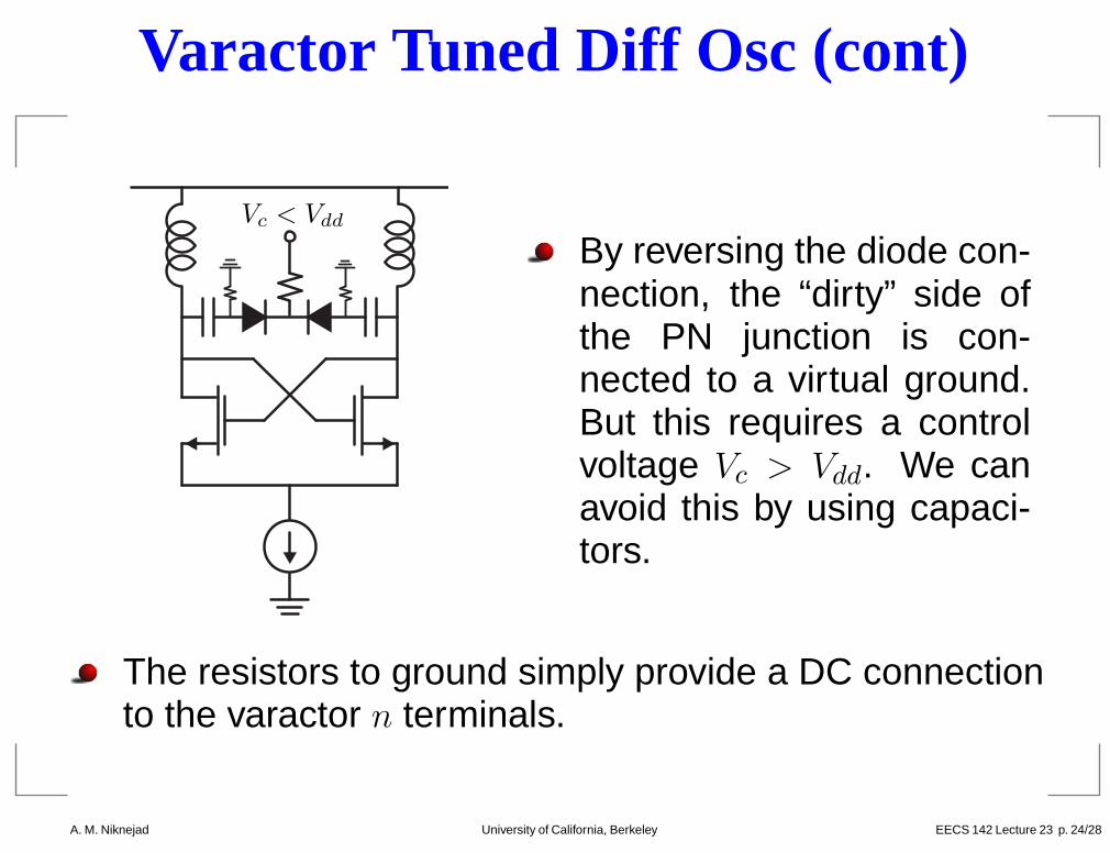
Varactor Tuned Diff Osc (cont)
Vc < Vdd
By reversing the diode con-nection, the “dirty” side ofthe PN junction is con-nected to a virtual ground.But this requires a controlvoltage Vc > Vdd. We canavoid this by using capaci-tors.
The resistors to ground simply provide a DC connectionto the varactor n terminals.
A. M. Niknejad University of California, Berkeley EECS 142 Lecture 23 p. 24/28 – p
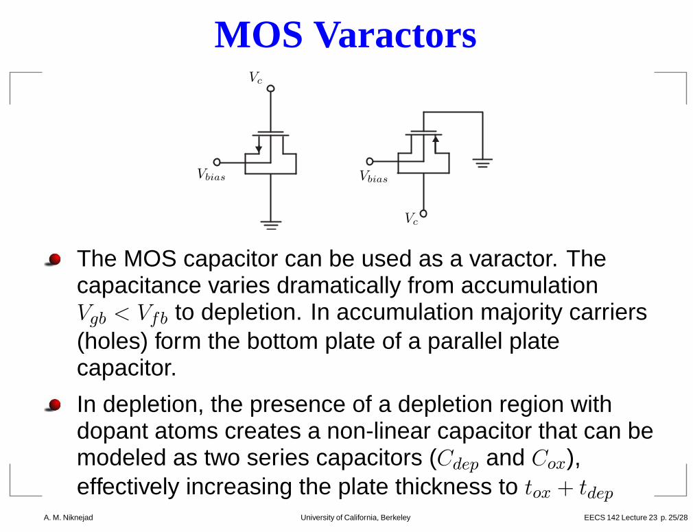
MOS VaractorsVc
Vc
Vbias Vbias
The MOS capacitor can be used as a varactor. Thecapacitance varies dramatically from accumulationVgb < Vfb to depletion. In accumulation majority carriers(holes) form the bottom plate of a parallel platecapacitor.
In depletion, the presence of a depletion region withdopant atoms creates a non-linear capacitor that can bemodeled as two series capacitors (Cdep and Cox),effectively increasing the plate thickness to tox + tdep
A. M. Niknejad University of California, Berkeley EECS 142 Lecture 23 p. 25/28 – p

MOS Varactor (Inversion)
actu
al
VFB VT
Cox
For a quasi-static excitation, thermal generation leads tominority carrier generation. Thus the channel will invertfor VGB > VT and the capacitance will return to Cox.
The transition around threshold is very rapid. If aMOSFET MOS-C structure is used (with source/drainjunctions), then minority carriers are injected from thejunctions and the high-frequency capacitance includesthe inversion transition.
A. M. Niknejad University of California, Berkeley EECS 142 Lecture 23 p. 26/28 – p

Accumulation Mode MOS Varactors
n-well
n+ n+
The best varactors are accumulation mode electronMOS-C structures. The electrons have higher mobilitythan holes leading to lower series resistance, and thusa larger Q factor.
Notice that this structure cannot go into inversion athigh frequency due to the limited thermal generation ofminority carriers.
A. M. Niknejad University of California, Berkeley EECS 142 Lecture 23 p. 27/28 – p
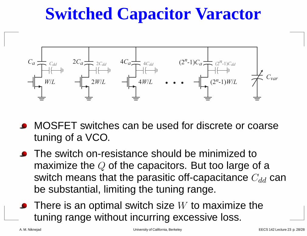
Switched Capacitor Varactor
Ca CddCC
W/L
2Ca 2CddCC
2W/L
4Ca 4CddCC
4W/L
(2n-1)Ca (2n-1)CddCC
(2n-1)W/LCvar
MOSFET switches can be used for discrete or coarsetuning of a VCO.
The switch on-resistance should be minimized tomaximize the Q of the capacitors. But too large of aswitch means that the parasitic off-capacitance Cdd canbe substantial, limiting the tuning range.
There is an optimal switch size W to maximize thetuning range without incurring excessive loss.
A. M. Niknejad University of California, Berkeley EECS 142 Lecture 23 p. 28/28 – p


