

Electromagnetic Modeling of Multi-Dimensional Scale Problems: Nanoscale SolarMaterials, RF Electronics, Wearable Antennas
Item Type text; Electronic Dissertation
Authors Yoo, Sungjong
Publisher The University of Arizona.
Rights Copyright © is held by the author. Digital access to this materialis made possible by the University Libraries, University of Arizona.Further transmission, reproduction or presentation (such aspublic display or performance) of protected items is prohibitedexcept with permission of the author.
Download date 05/07/2018 02:22:53
Link to Item http://hdl.handle.net/10150/333484
ELECTROMAGNETIC MODELING OF MULTI-DIMENSIONAL
SCALE PROBLEMS:
NANOSCALE SOLAR MATERIALS, RF ELECTRONICS,
WEARABLE ANTENNAS
by
Sungjong Yoo
________________________
Copyright © Sungjong Yoo
A Dissertation Submitted to the Faculty of the
DEPARTMENT OF ELECTRICAL AND COMPUTER ENGINEERING
In Partial Fulfillment of the Requirements
For the Degree of
DOCTOR OF PHILOSOPHY
In the Graduate College
THE UNIVERSITY OF ARIZONA
2014

2
THE UNIVERSITY OF ARIZONA
GRADUATE COLLEGE
As members of the Dissertation Committee, we certify that we have read the dissertation
prepared by Sungjong Yoo
entitled Electromagnetic Modeling of Multi-Dimensional Scale problems:
Nanoscale Solar Materials, RF electronics, Wearable antennas
and recommend that it be accepted as fulfilling the dissertation requirement for the Degree of
Doctor of Philosophy
__________________________________________________________Date: 06/25/2014
Kathleen L. Melde, Ph.D
__________________________________________________________Date: 06/25/2014
Kelly S. Potter, Ph.D
__________________________________________________________Date: 06/25/2014
Janet Roveda, Ph.D
Final approval and acceptance of this dissertation is contingent upon the candidate's submission
of the final copies of the dissertation to the Graduate College.
I hereby certify that I have read this dissertation prepared under my direction and recommend
that it be accepted as fulfilling the dissertation requirement.
__________________________________________________________Date: 06/25/2014
Dissertation Director: Kathleen L. Melde

3
STATEMENT BY AUTHOR
This dissertation has been submitted in partial fulfillment of requirements for an advanced
degree at The University of Arizona and is deposited in the University Library to be made
available to borrowers under rules of the Library.
Brief quotations from this dissertation are allowable without special permission, provided
that accurate acknowledgment of source is made. Requests for permission for extended
quotation from or reproduction of this manuscript in whole or in part may be granted by the head
of the major department or the Dean of the Graduate College when in his or her judgment the
proposed use of the material is in the interests of scholarship. In all other instances, however,
permission must be obtained from the copyright holder.
SIGNED: _________________________________
Sungjong Yoo

4
ACKNOWLEDGEMENTS
I would like to express my deepest gratitude to Professor Kathleen Melde, for the constant
support, technical discussions, contribution to this work, and encouragement she provided me for
the past five years.
I would like to thank my committee members, Prof. Kelly Potter and Prof. Janet Roveda for
spending time in attending my dissertation defense; having feedbacks and corrections on my
dissertation. I am grateful to Prof. Joan Redwing and Dr. Chito Kendrick for providing great data
and information about the nanowire and branched nanowire solar cell. I owe special thanks to Dr.
Ho-Hsin Yeh from Qualcomm and Nobuki Hiramatsu from Kyocera for providing me the
artificial magnetic conductor technology and 60 GHz antenna design experience.
I would like to thank to all group members in the high frequency packaging and antenna
design lab at the University of Arizona: Marcos Vargas, Arghya Sain, and Reshmaa Liyakatha. I
owe special thanks to Marcos Vargas for sharing a lot of industrial experience with me to help
my research. I had lots of fun being a member of this fantastic group.
I would like to thank for generous financial support from National Science Foundation
(NSF), which made this research possible.
I would like to express my gratitude and love to my family members; my mother, father who
is in heaven, brother and sister-in-law, and my mother-in-law. Thank you for your unlimited
support, love and prayers. I thank God for granting me such a wonderful family.
Last, but not least, I thank my lovely wife Aran Kim. Your unconditional love,
encouragement, and prayers helped me through my Ph.D study and I am thankful to God for our
marriage and our unborn daughter. I am not who I am without you. I love you.

5
TABLE OF CONTENTS
LIST OF FIGURES .......................................................................................................... 8
LIST OF TABLES .......................................................................................................... 12
ABSTRACT ..................................................................................................................... 13
CHAPTER 1 INTRODUCTION ................................................................................... 15
1.1 Computational Simulation Electromagnetic Modeling Tool .................................. 16
1.2 Silicon Branched nanowire Photovoltaic ................................................................ 18
1.3 Wireless Communication for Multi-Chip Multi-Core System ............................... 22
1.4 Zigzag Antenna ....................................................................................................... 25
1.5 Research Objective ................................................................................................. 27
1.6 Dissertation Outline ................................................................................................ 28
CHAPTER 2 COMPUTATIONAL DESIGN OF BRANCHED NANOWIRE
STRUCTURES FOR PHOTOVOLTAICS .................................................................. 29
2.1 Silicon Characteristics as a Material of Photovoltaic ............................................. 29
2.2 Silicon PV Cell Mechanisms ................................................................................. 31
2.2.1 Light Trapping of Silicon ............................................................................... 31
2.2.2 Flat Silicon PV Operation .............................................................................. 33
2.2.3 Silicon PV Design Parameters ....................................................................... 34
2.2.4 Flat Silicon PV Efficiency .............................................................................. 38
2.3 Silicon PV Cell Parameters as a Circuit System .................................................... 39

6
2.3.1 External Quantum Efficiency ......................................................................... 40
2.3.2 Silicon PV Fill Factor and Efficiency ............................................................ 41
2.4 Current State of Art on Nanostructured Silicon PV................................................ 44
2.4.1 Current State of Art ........................................................................................ 44
2.4.2 NW and BNW Fabrication ............................................................................. 48
2.5 Electromagnetic Computational Design for PV with Silicon Branch NW ............. 49
2.5.1 Maxwell’s Equations and Boundary Conditions ............................................ 49
2.5.2 Full Wave EM Modeling Computational Simulation Tools .......................... 51
2.5.3 MEEP and HFSS Verification ........................................................................ 53
2.5.4 MEEP and HFSS BNW Design Comparison ................................................. 58
2.6 Effect of Branches on the Reflection of BNW ....................................................... 60
CHAPTER 3 DESIGN OF 60-GHZ ANTENNA ARRAY FOR MULTI-CHIP
COMMUNICATION ...................................................................................................... 69
3.1 Introduction ............................................................................................................. 69
3.2 Current States of Art ............................................................................................... 70
3.3 Reconfigurable four elements array for MCMC system......................................... 81
3.4 Comparison of 4 Antennas Array on AMC layer with the Ring Shape and with the Star
Shape ............................................................................................................................. 84
3.4.1 Antenna Separation Factor Determination ..................................................... 84
3.4.2 Gain Patterns of Four Elements Array from Ring and Star Orientation ........ 88
3.5 Four Element Antennas Array Design .................................................................... 90
3.5.1 Initial Patch and Antenna Design ................................................................... 90
3.5.2 Antenna Optimization Process ....................................................................... 94

7
3.6 Results Analysis ...................................................................................................... 97
CHAPTER 4 GENERALIZATION OF VHF ZIGZAG ANTENNA ...................... 102
4.1 Introduction ........................................................................................................... 102
4.2 Zigzag Antenna Design Process ........................................................................... 107
4.2.1 Small Ground Effects ................................................................................... 107
4.2.2 Meandering the Antenna to the Zigzag Shape ............................................. 113
4.2.3 Antenna Input Impedance Matching Methods ............................................. 113
4.3 Polar Bear Tracking Antenna................................................................................ 119
4.3.1 Upright Zigzag Antenna for Polar Bear ....................................................... 123
4.3.2 Curved Zigzag Antenna for Polar Bear Body Material ................................ 125
4.3.3 Radiation Efficiency of Zigzag Antenna ...................................................... 131
4.3.4 Specific Absoprtion Rate (SAR) of the Zigzag Antenna ............................. 134
4.4 Antenna Fabrication .............................................................................................. 135
CHAPTER 5 CONCLUSIONS .................................................................................... 137
5.1 Completed Works ............................................................................................. 137
5.2 Future Works .................................................................................................... 139
APPENDIX A ANOTHER APPROACH OF SEPARATION FACTOR ............... 142
REFERENCES .............................................................................................................. 144

8
LIST OF FIGURES
Fig. 1-1 Three areas of full wave EM tool applications in broad frequency range .......... 15
Fig. 1-2 Consumption of (a) world energy and (b) CO2 emission .................................... 19
Fig. 1-3 NREL solar cell efficiency chart [6] ................................................................... 20
Fig. 1-4 SEM pictures of (a) NW and (b) BNW ............................................................... 21
Fig. 1-5 Solar irradiance of AM 1.5 vs. wavelength ......................................................... 22
Fig. 1-6 Computation hierarchy inside the HPC system................................................... 24
Fig. 1-7 Predicted size on the semiconductor [12] ........................................................... 24
Fig. 1-8 MCMC wireless communication system [13] ..................................................... 25
Fig. 1-9 Model of animal tracking system with dog collar and handheld[16] .................. 26
Fig. 1-10 Wave attenuation in forested regions as a function of frequency ..................... 26
Fig. 2-1 Abundance of the Earth elements ........................................................................ 29
Fig. 2-2 Frequency dependent refraction index of (a) c-Si and (b) a-Si:H ....................... 30
Fig. 2-3 Solar wave spectrums (a) at AM1.5 (b) along to wavelength (c) along to
photon energy (d) along to frequency ............................................................................... 32
Fig. 2-4 Light trapping mechanism ................................................................................... 33
Fig. 2-5 Flat Silicon PV cell structure .............................................................................. 34
Fig. 2-6 P-N junction (a) non-equilibrium state (b) equilibrium state .............................. 35
Fig. 2-7 External Quantum Efficiency .............................................................................. 41
Fig. 2-8 Equivalent circuit of an ideal PV cell ................................................................ 42
Fig. 2-9 IV curve of general PV cell ................................................................................. 43
Fig. 2-10 Evolution of nanostructured Si solar cells (a) black silicon (b) NW (c) BNW . 44
Fig. 2-11 Optical path length of (a) Flat substrate (b) Black silicon substrate ................. 45
Fig. 2-12 PV cell structures of (a) NW (b) BNW ............................................................. 47
Fig. 2-13 Schematic of BNW fabrication process (a) patterned substrate (b) VLS
growth of Si NW trunks (c) metal diffusion or deposition (d) VLS growth of Si NW
branches ............................................................................................................................ 49
Fig. 2-14 FDTD method (a) FDTD process (b) Yee’s lattice ........................................... 52
Fig. 2-15 FEM (a) Analysis Algorithm (b) Meshes .......................................................... 53
Fig. 2-16 Effect of rectangular waveguide (a) traditional method (b) current method..... 54
Fig. 2-17 NW PV unit cell with periodic structures ......................................................... 55
Fig. 2-18 Absorption comparisons of NWs with 1.16 µm, 2.33 µm, and 4.66 µm
and film, and reflection and transmittance comparisons of NWs with 2.33 µm
and film (a) absorption from TMM [37] (b) reflection and transmittance from
TMM [37] (c) absorption from MEEP (d) reflection and transmittance from MEEP
(e) absorption from HFSS (f) reflection and transmittance from HFSS .......................... 56

9
LIST OF FIGURES - CONTINUED
Fig. 2-19 (a)The time usage of MEEP and HFSS and (b) memory usage of MEEP
and HFSS .......................................................................................................................... 57
Fig. 2-20 BNW PV unit cell with periodic structures (a) MEEP (b) HFSS ..................... 59
Fig. 2-21 BNW PV modeling results of (a) reflection and (b) absorption ....................... 60
Fig. 2-22 Thin substrate with ABC approximation to the thick substrate ........................ 61
Fig. 2-23 Comparison of optical reflectivity from HFSS simulation, measurement, and
calculation ......................................................................................................................... 62
Fig. 2-24 Unit Cell of NW structures (a) planar (b) 19 μm (c) 32.3 μm ........................ 63
Fig. 2-25 Optical reflections of three different NW lengths from HFSS simulation ........ 63
Fig. 2-26 Optical reflections of three different branch lengths from measurement .......... 64
Fig. 2-27 Unit Cell of BNW structures with different branch lengths (a) 1 µm (b) 3 µm
(c) 5 µm ............................................................................................................................. 65
Fig. 2-28 Optical reflections of three different branch lengths from HFSS simulation ... 66
Fig. 2-29 Optical reflections of three different branch lengths from measurement .......... 66
Fig. 2-30 Unit Cell of BNW structures with different branch directions(a) 100 %
(b) 0 % (c) 50 % ................................................................................................................ 67
Fig. 2-31 Optical reflections of three different branch directions from HFSS simulation 66 Fig. 3-1 Antenna in Package prifole [54].......................................................................... 70
Fig. 3-2 Profiles of (a) mushroom-like AMC layer and (b) periodically-patched AMC
layer................................................................................................................................... 72
Fig. 3-3 Reflection phases of mushroom-like AMC and periodically-patched AMC
layer................................................................................................................................... 72
Fig. 3-4 Design parameters of AMC layer ........................................................................ 73
Fig. 3-5 Waveguide simulator setup to predict values of reflection phase ....................... 74
Fig. 3-6 Reflection phase of periodic-patch AMC layered ground plane ......................... 75
Fig. 3-7 Multi-chip multi-core system with wireless link antenna [14] ........................... 75
Fig. 3-8 Two elements array antenna [61] ........................................................................ 76
Fig. 3-9 Overall multi-chip communication system with two elements array .................. 77
Fig. 3-10 (a) Simulated and measured performances on the reflection coefficient S11 (b)
measurement setup ............................................................................................................ 77
Fig. 3-11 Wireless link communication system ................................................................ 78
Fig. 3-12 Wireless link performance of current state of art comparison (a) power loss
required to be recovered (b) budget .................................................................................. 80
Fig. 3-13 Expected gain pattern of a router to the neighbor routers ................................. 82
Fig. 3-14 Gain pattern created from two identical antennas ............................................. 83

10
LIST OF FIGURES - CONTINUED
Fig. 3-15 Four antenna orientations (a) ring shape (b) star shape .................................... 83
Fig. 3-16 Multi-chip multi-core system with wireless link antenna [14] ......................... 84
Fig. 3-17 Far-field approximation (a) ring (b) star ........................................................... 86
Fig. 3-18 Far field vector simplification ........................................................................... 86
Fig. 3-19 Array factor plots along to the distance between the antenna feeding points ... 88
Fig. 3-20 Simulated dimensions of four elements array from (a) ring and(b) star
orientation ......................................................................................................................... 88
Fig. 3-21 Gain patterns of (a) single and (b) two antennas from the ring and star
orientations ........................................................................................................................ 90
Fig. 3-22 Unit structure and dimensions of periodic AMC layer ..................................... 91
Fig. 3-23 Reflection phase with different W .................................................................... 91
Fig. 3-24 Four antenna array with the dimension of the AMC layer (a) top view
(b) profile .......................................................................................................................... 92
Fig. 3-25 Gain pattern of four array antenna with the initial values of W, antl, and antw 93
Fig. 3-26 Input impedance of four array antenna with the initial values of W, antl, and
antw .................................................................................................................................... 93
Fig. 3-27 Directive gain pattern of case 1 and case 2 (a) two antennas-on
(b) one antenna-on ........................................................................................................... 98
Fig. 3-28 Input impedance of (a) case 1 (b) case 2 ........................................................... 99
Fig. 3-29 Reflection coefficient of case 1 and case 2 ..................................................... 100
Fig. 3-30 Wireless link performance comparison (a) power loss required to be
recovered (b) budget ....................................................................................................... 101
Fig. 4-1 Model of animal tracking system with dog collar and handheld ...................... 103
Fig. 4-2 Wave attenuation in forested regions as a function of frequency ..................... 104
Fig. 4-3 Upright zigzag antenna...................................................................................... 105
Fig. 4-4 Collar integrated zigzag antenna ....................................................................... 106
Fig. 4-5 Monopole antenna on the small ground plane .................................................. 108 Fig. 4-6 Return loss of monopole antenna on the small ground plane and infinite
ground plane.................................................................................................................... 109
Fig. 4-7 E-field pattern of the monopole antenna on the infinite ground plane (top)
and small ground plane (bottom) (a) XY plane (b) YZ plane (c) ZX plane ................... 112
Fig. 4-8 Geometry of an upright zigzag antenna ............................................................ 114
Fig. 4-9 Four antennas with different L1 and N=1(a) L1 =0 (b) L1 =L/10=48.12 mm
(c) L1 =L/5=96.24 mm (d) L1 =L/2=240.6 mm .............................................................. 114

11
LIST OF FIGURES - CONTINUED
Fig. 4-10 Impact of adding zigzag sections .................................................................... 117
Fig. 4-11 Length tuning method ..................................................................................... 118 Fig. 4-12 Depiction of current flow on (a) antenna without shorting pin and
(b) antenna with a shorting pin ....................................................................................... 119
Fig. 4-13 Comparison of the effect of shorting pin length on the current distribution
on monopole antennas (shorting pin height is 15 mm) (a) total current distribution
(b) current distribution near the feed ............................................................................. 120
Fig. 4-14 (a) Resistance (b) Reactance of antennas with different length of
shorting pins .................................................................................................................... 122
Fig. 4-15 Four antennas with different N (α=60˚, and total length=473 mm) (a) N=0
(b) N =5 (c) N=10 (d) N=15 ........................................................................................... 124
Fig. 4-16 Final design of upright zigzag ......................................................................... 125
Fig. 4-17 Dielectric properties of the body material ....................................................... 126
Fig. 4-18 Input impedance change by meandering ......................................................... 127
Fig. 4-19 Final collar integrated zigzag antenna configuration ...................................... 127
Fig. 4-20 Input impedance change of curved zigzag near animal body by length
tuning .............................................................................................................................. 128
Fig. 4-21 Input impedance change of curved zigzag near animal body by length
tuning and shorting pin ................................................................................................... 129
Fig. 4-22 10 dB bandwidth of the zigzag antenna .......................................................... 130
Fig. 4-23 Radiation pattern of the zigzag antenna .......................................................... 131
Fig. 4-24 Equivalent circuit of antenna impedance ........................................................ 131
Fig. 4-25 Wheeler cap method diagram (a) antenna without Wheeler cap
(b) antenna with Wheeler cap ......................................................................................... 133
Fig. 4-26 SAR field plot of the Zigzag antenna on the body phantom ........................... 135
Fig. 4-27 Curved zigzag antenna with collar .................................................................. 136
Fig. 4-28 Comparison of HFSS models and curved zigzag antenna with collar,
phantom, tuning part, and shorting pin ........................................................................... 136
Fig. 5-1 Irregular branched NW...................................................................................... 139
Fig. 5-2 Waveport feeding antenna package................................................................... 140
Fig. 5-3 Multi-line multi-layer zigzag antenna ............................................................... 141
Fig. A-1 Four element antennas array in the spherical coordinate system of (a) ring
(b) star ............................................................................................................................. 142
Fig. A-2 Array factor plots along to the distance between the antenna feeding points .. 143

12
LIST OF TABLES
Table 2-1 Time Harmonic Maxwell’s equation ................................................................ 49
Table 2-2 Design Parameters of BNW ............................................................................. 59 Table 3-1 Dimension parameters of AMC layer............................................................... 74 Table 3-2 Gain and bandwidth of current state of art ....................................................... 79 Table 3-3 Values and directions of four elements array antenna gain .............................. 90 Table 3-4 Parametric study of antenna characteristics with W ......................................... 95
Table 3-5 Parametric study of antenna characteristics with antl, when W = 0.65 mm ..... 96
Table 3-6 Parametric study of antenna characteristics with antw when W = 0.65 mm
and antl = 1 mm ................................................................................................................. 96
Table 3-7 Parametric study of antenna characteristics with antw when W = 0.65 mm
and antl = 1.2 mm .............................................................................................................. 97 Table 3-8 Results comparison of case 1 and case 2 .......................................................... 98 Table 4-1 MURS frequency designation ........................................................................ 104 Table 4-2 Antenna characteristics of the monopole antenna on an ............................... 109
Table 4-3 Comparison of simulation results from four zigzag antennas with different
L1 .................................................................................................................................... 115 Table 4-4 Antenna characteristics with different angles of zigzag ................................. 116
Table 4-5 Antenna characteristics of 473.04 mm and 513.3 mm monopole antennas ... 117 Table 4-6 Input impedance of antenna as a function of 15 mm height and different
length of shorting pin ...................................................................................................... 121
Table 4-7 Input impedance and W2 with different N
(α=60˚, and total length=473 mm) .................................................................................. 124
Table A-1 Antenna feeding point positions .................................................................... 141

13
ABSTRACT
The use of full wave electromagnetic modeling and simulation tools allows for accurate
performance predictions of unique RF structures that exhibit multi-dimensional scales. Full wave
simulation tools need to cover the broad range of frequency including RF and terahertz bands that
is focused as RF technology is developed. In this dissertation, three structures with multi-
dimensional scales and different operating frequency ranges are modeled and simulated.
The first structure involves nanostructured solar cells. The silicon solar cell design is
interesting research to cover terahertz frequency range in terms of the economic and
environmental aspects. Two unique solar cell surfaces, nanowire and branched nanowire are
modeled and simulated. The surface of nanowire is modeled with two full wave simulators and
the results are well-matched to the reference results. This dissertation compares and contrasts the
simulators and their suitability for extensive simulation studies. Nanostructured Si cells have large
and small dimensional scales and the material characteristics of Si change rapidly over the solar
spectrum.
The second structure is a reconfigurable four element antenna array antenna operating at 60
GHz for wireless communications between computing cores in high performance computing
systems. The array is reconfigurable, provides improved transmission gain between cores, and can
be used to create a more failure resilient computing system. The on-chip antenna array involves
modeling the design of a specially designed ground plane that acts as an artificial magnetic
conductor. The work involves modeling antennas in a complex computing environment.

14
The third structure is a unique collar integrated zig-zag antenna that operates at 154.5 MHz
for use as a ground link in a GPS based location system for wildlife tracking. In this problem, an
intricate antenna is modeled in the proximity of an animal. Besides placing a low frequency
antenna in a constricted area (the collar), the antenna performance near the large animal body
must also be considered.
Each of these applications requires special modeling details to take into account the various
dimensional scales of the structures and interaction with complex media. An analysis of the
challenges and limits of each specific problem will be presented.
15
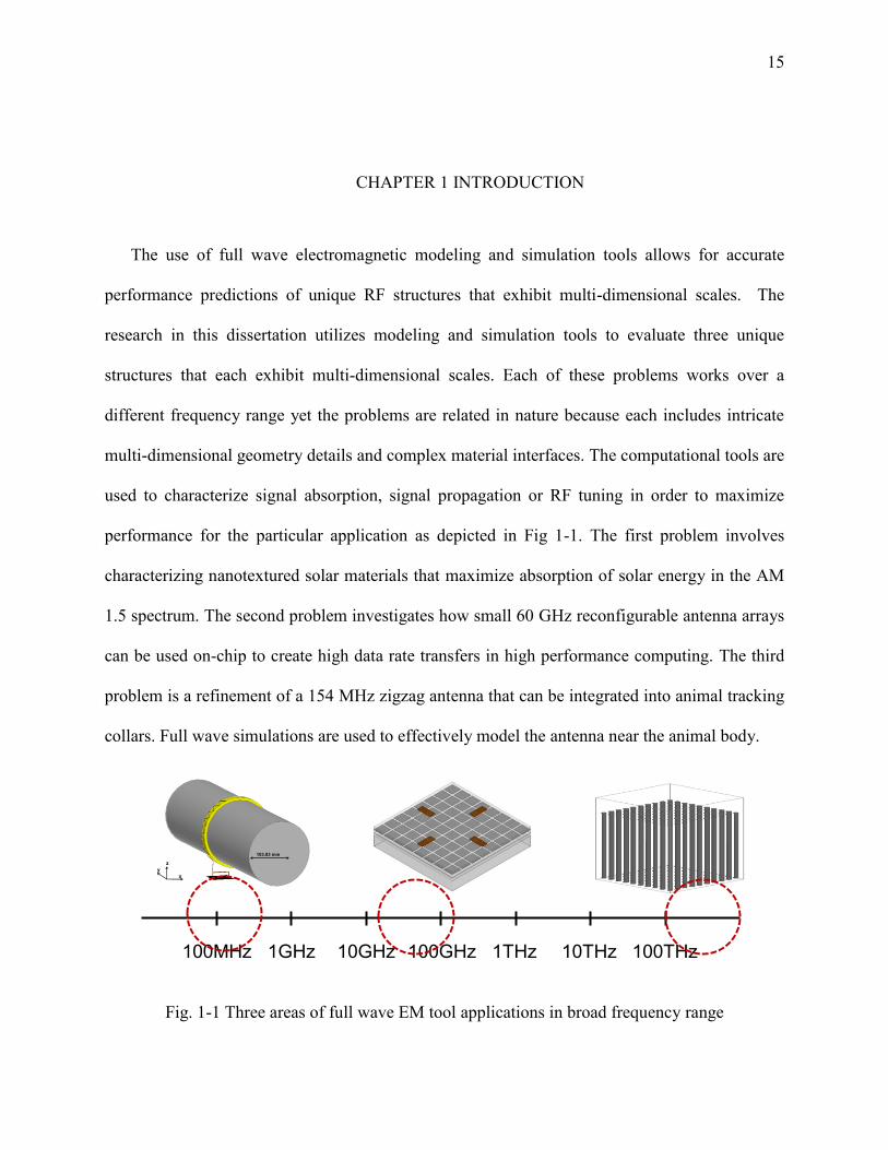
CHAPTER 1 INTRODUCTION
The use of full wave electromagnetic modeling and simulation tools allows for accurate
performance predictions of unique RF structures that exhibit multi-dimensional scales. The
research in this dissertation utilizes modeling and simulation tools to evaluate three unique
structures that each exhibit multi-dimensional scales. Each of these problems works over a
different frequency range yet the problems are related in nature because each includes intricate
multi-dimensional geometry details and complex material interfaces. The computational tools are
used to characterize signal absorption, signal propagation or RF tuning in order to maximize
performance for the particular application as depicted in Fig 1-1. The first problem involves
characterizing nanotextured solar materials that maximize absorption of solar energy in the AM
1.5 spectrum. The second problem investigates how small 60 GHz reconfigurable antenna arrays
can be used on-chip to create high data rate transfers in high performance computing. The third
problem is a refinement of a 154 MHz zigzag antenna that can be integrated into animal tracking
collars. Full wave simulations are used to effectively model the antenna near the animal body.
Fig. 1-1 Three areas of full wave EM tool applications in broad frequency range
100MHz 1GHz 10GHz 100GHz 1THz 10THz 100THz
103.83 mm
x
y
z

16
Radio frequency (RF) technology is defined as a frequency range from 3 kHz to 300 GHz
and is prevalent in cell phones, satellites, PCs, etc. Terahertz waves occupy the frequency range
of tremendously high frequencies (THF) from 300 GHz to 3000 GHz [1]. It is also called the
submillimeter wave because the wavelength of THF is less than or equal to1 mm. The terahertz
wave penetrates through non-conducting materials such as clothes, plastics, or ceramics.
Terahertz frequencies are popular in medical imaging because the penetration of terahertz waves
is deeper than the X-ray and the magnetic resonance imaging (MRI) without any hazardous
effect on the bio-tissues or DNAs.
1.1 Computational Simulation Electromagnetic Modeling Tools
The computational simulation electromagnetic (EM) modeling tools covering the range from
RF to terahertz waves save considerable time and effort for advanced EM research. Researchers
are able to predict the behavior of new structures over a broad-range of frequencies, and reduce
the possible mistakes in the discovery stage. EM simulation technology has been prevalent for
over 20 years and has been instrumental in the rapid advancement of new antenna and packaging
research. Full wave tools have been extensively verified by experiments for numerous
applications. One advantage of full wave tools is that a user can master the tool without
significant prior knowledge of expected performance or outcomes of the structure to be modeled.
Simulation methods based upon reduced order models, wire grid models, or equivalent circuit
models require sufficient background on the expected structures in order to create an accurate
model. Full wave EM tools allow for multi-scale dimensions, frequency dependent material

17
characteristics, visual graphical based geometry modeling, and versatile graphical displays of
output results. Significant design elements of EM modeling tools are the material characteristics,
boundary conditions, the operating frequency, and the structural dimension. Characteristics of
materials such as the dielectric constant, the conductivity, and the loss tangent determine the
electric properties of the materials. The material characteristics are not single values because
they are frequency dependent properties. Boundary conditions assigned on the objects determine
the behaviors of EM waves at the interface of objects. Improper boundary conditions assigned
cause errors on the surfaces. Operating frequencies and structural dimensions impact simulation
time and memory. The objects with dimensions considerably greater than the operating
wavelength result in the huge time and memory consumption. Selecting an appropriate modeling
strategy for analysis to save simulation time and memory is also important as well as the
structure design.
The EM simulation tools are expected to operate over broad-range frequencies, from
megahertz to terahertz, with reasonable frequency dependent material characteristics. In this
dissertation, three electromagnetic structures operating at different frequency ranges are
introduced and simulated by a computational simulation EM modeling tool. The EM
characteristics, design issues, and methodology to solve the given problems are explained.
The EM simulation tools can be applied to terahertz frequency devices such as photovoltaics
(PVs). PVs are a promising renewable energy source in terms of the economy and environment.
Low efficiency is a roadblock for broad commercialization of PV products. The application of
useful computer simulation tools will help the development of solar energy research. The time
18
and memory issues caused by relatively larger objects than the operating wavelength are
described and the solution is suggested.
A reconfigurable 60 GHz low profile on-chip antenna array for chip-to-chip data transfers is
an example of an antenna operating at a mid-range frequency. The principle of an artificial
magnetic conductor (AMC) layer is introduced to solve the source current cancelled by the
image current generation near a perfect electric conductor (PEC) is discussed. The
reconfigurable radiation pattern is created by four array antennas.
Another interesting RF research is a very high frequency (VHF) antenna technology that is a
relatively low frequency antenna. The longer wavelength with longer propagation distance over
the ground link reduces the intercept of the external natural surroundings with less attenuation of
the wave [2]. The disadvantage of a VHF antenna is a larger size compared to higher frequency
antennas because of the longer wavelength. The VHF collar zigzag antenna is one of the
solutions for the VHF antenna with small dimension. The design process of the zigzag antenna is
introduced in [3]. The design properties of VHF zigzag antenna are thoroughly analyzed in terms
of input impedance in Chapter 4.
1.2 Silicon Branched Nanowire Silicon Photovoltaic Materials
The energy consumption generated by nonrenewable fossil fuels has been increased as the
energy technology has rapidly advanced. The amount of carbon dioxide emission that is the
byproduct of burning fossil fuels also has been increased. It causes a significant problem because
the emitted carbon dioxide gas destroys the natural environment. The world energy consumption
19
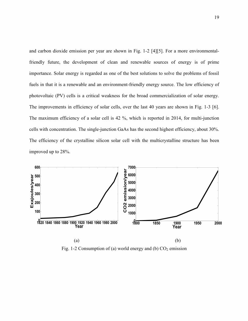
and carbon dioxide emission per year are shown in Fig. 1-2 [4][5]. For a more environmental-
friendly future, the development of clean and renewable sources of energy is of prime
importance. Solar energy is regarded as one of the best solutions to solve the problems of fossil
fuels in that it is a renewable and an environment-friendly energy source. The low efficiency of
photovoltaic (PV) cells is a critical weakness for the broad commercialization of solar energy.
The improvements in efficiency of solar cells, over the last 40 years are shown in Fig. 1-3 [6].
The maximum efficiency of a solar cell is 42 %, which is reported in 2014, for multi-junction
cells with concentration. The single-junction GaAs has the second highest efficiency, about 30%.
The efficiency of the crystalline silicon solar cell with the multicrystalline structure has been
improved up to 28%.
(a) (b)
Fig. 1-2 Consumption of (a) world energy and (b) CO2 emission
1820 1840 1860 1880 1900 1920 1940 1960 1980 20000
100
200
300
400
500
600
Year
Exajo
ule
s/y
ear
1800 1850 1900 1950 20000
1000
2000
3000
4000
5000
6000
7000
Year
CO
2 e
mis
sio
n/y
ear

20
Fig. 1-3 NREL solar cell efficiency chart [6]
Nanostructured silicon solar cells will be discussed in this dissertation due to the economic
advantage, discussed in Chapter 2. Efficiency of the PVs can be improved by increasing the light
trapping ability and electron extraction efficiency of these devices [6][7]. The use of silicon
nanowire (NW) and branched nanowire (BNW) arrays on the silicon substrate of PVs is one
suggested way of improving the efficiency of PVs. The definitions and principles of NW and
BNW are introduced in Chapter 2. The SEM picture of NW and BNW are shown in Fig. 1-4.

21
(a) (b)
Fig. 1-4 SEM pictures of (a) NW and (b) BNW
In Chapter 2, two computational electromagnetic (EM) modeling tools to simulate the PVs
with a silicon BNW array are introduced: the finite-element method (FEM) and the finite-
difference time-domain (FDTD) approach. The rationale behind the use of full wave EM tools to
simulate PVs is discussed. The periodic structure of a NW array consumes a lot of memory, so
simulations using a unit cell and periodic boundary conditions are utilized to reduce the model
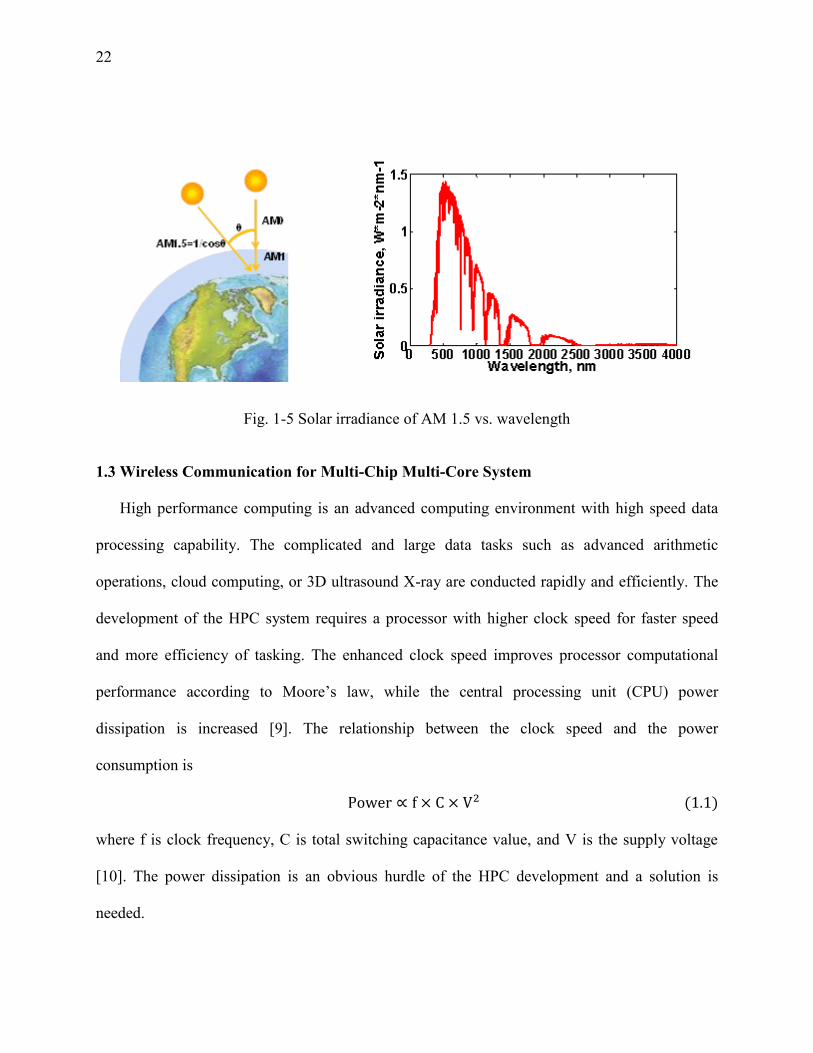
size. The solar irradiance over the solar energy spectrum is shown in Fig. 1-5. The simulation
results are analyzed and compared to the references for accuracy.
[1] [2] [3]
22
Fig. 1-5 Solar irradiance of AM 1.5 vs. wavelength
1.3 Wireless Communication for Multi-Chip Multi-Core System
High performance computing is an advanced computing environment with high speed data
processing capability. The complicated and large data tasks such as advanced arithmetic
operations, cloud computing, or 3D ultrasound X-ray are conducted rapidly and efficiently. The
development of the HPC system requires a processor with higher clock speed for faster speed
and more efficiency of tasking. The enhanced clock speed improves processor computational
performance according to Moore’s law, while the central processing unit (CPU) power
dissipation is increased [9]. The relationship between the clock speed and the power
consumption is
where f is clock frequency, C is total switching capacitance value, and V is the supply voltage
[10]. The power dissipation is an obvious hurdle of the HPC development and a solution is
needed.

23
The design of multi-chip, multi-core (MCMC) systems is a promising processor due to low
CPU power dissipation. An example of the computation hierarchy of the MCMC inside HPC
system is shown in Fig. 1-6. The computational performances are enhanced by the computer
architecture with 100 processor chips on a single package massive data cluster module. Each
single processor chip consists of two or more individual CPU or cores operating with parallel
processing for the capabilities of read and write. The instructions of a CPU are performed by the
parallel computing of all instructions simultaneously. The large amount of data tasks is divided
into the number of cores and conducted in the parallel computing process [11]. The clock time of
multi-core architecture used to perform the CPU instruction is less than the single core system.
The performance of a processor is enhanced and power consumption is reduced as each core runs
at the same time. A supercomputer with an HPC system consists of multiple processor chips
fabricated in a single computing package module, while multiple CPUs are integrated in each
single processor chip.
The individual cores in a chip communicate to each other for I/O data transfer by physical wire-
bonding. Wire-bonding is a broadly used wire interconnects method because of the advantages in
cost and flexibility. However, the wire-bonding is not an appropriate method for interconnect
between the small chips. The existence of wire connection causes mutual coupling such as
crosstalk, parasitic inductance and capacitance, or high signal noise ratio (SNR), which affects
on the data communication as the dimensions of CPUs are getting smaller. The rate of I/O pitch
size reduction is less than the rate of chip size reduction, which causes as shown in Fig. 1-7 [12].

24
Data Cluster Multi-Chip in the Module Multi-Core in the Single Chip
Fig. 1-6 Computation hierarchy inside the HPC system
A millimeter wireless link for the data communication system is investigated to solve the
problems of the I/O pitch scaling down and the crosstalk between adjacent wires as shown in
Fig.1-8 [13]. In the suggested system, nine cores are connected with wire-bonding and on-chip
antenna is fabricated on the center core, a router. The router does the wireless communication
with other routers in neighbor group of cores. The low profile antenna operating at 60 GHz is
selected for the 15% -10 dB reflection coefficient bandwidth, which enables about 20 Gbps data
transfer [14].
Fig. 1-7 Predicted chip size and I/O pitch on the semiconductor [12]
2010 2012 2014 2016 2018 202020
40
60
80
100
120
140
160
180
200
Glo
bal in
terc
on
nect
pit
ch
, n
m
2010 2012 2014 2016 2018 202010
12
14
16
18
20
22
24
26
28
30
32
Time, year
Gate
len
gth
, n
m
Global interconnection pitch
Gate length

25
Fig. 1-8 MCMC wireless communication system [13]
1.4 Zigzag Antenna
An RF tracking device that incorporates wearable antennas mounted on the animals are used
for tracking their movements. A wildlife tracking system should use antennas that do not
interfere with the normal behavior of the animal. The wearable antenna is an appropriate
candidate antenna for the wildlife tracking system because of its low-profile, omni-directional
beam coverage in the horizontal direction, and adequate bandwidth performance [15]. The radio
systems used for wildlife monitoring are, in general, relatively low data rate and narrow
bandwidth compared to commercial handheld wireless systems used for human point-to-point
communications. The animal tracking system with the dog collar and the handset are shown in
Fig. 1-9 [16].
CORE
CORE
CORE
CORE
CORE
CORE
CORE
CORE
CORE
CORE
CORE
CORE
CORE
Router1
CORE
CORE
CORE
Antenna Directive Radiation Pattern
On chip antenna
Router2
CORE
CORE
CORE
CORE
CORE
CORE
CORE
CORE
CORE
CORE
CORE
CORE
CORE
Router3
CORE
CORE
CORE
Router4

26
Fig. 1-9 Model of animal tracking system with dog collar and handheld[16]
Fig. 1-10 Wave attenuation in forested regions as a function of frequency
GPS Link: Receive Only
L1, L2 & L5 Frequencies.
Ground Link Full-Duplex
Frequency Agile.
100 200 300 40010
-2
10-1
100
Frequency, MHz
Att
en
ua
tio
n,
dB
/m

27
The attenuation of signals in a forest increase when the operating frequency increases. It is
shown in Fig. 1-10 (which is listed in dB/meter) [17]. A wearable antenna operating at a
relatively low frequency is selected for the ground link of the animal tracking system because
natural environments have a lot of natural objects that significantly interfere with wave
propagation at higher frequencies. The antenna is tuned with the input impedance analysis of the
antenna with the EM tool in Chapter 4.
1.5 Research Objectives
The objective of this dissertation is to: 1) Introduce the various applications of a full wave
EM modeling simulation tool to the variety of multi-range frequency such as a PV design; 2)
Describe the design method for a reconfigurable four array on-chip antenna with the AMC layer;
3) Analyze the electromagnetic properties of a VHF wearable zigzag antenna with a shorting pin
in terms of input impedance.
Contributions of this Work
Created a computational framework for the EM modeling of nanostructured PV materials.
These materials are electrically large at THz frequencies. The material characteristics of
Si change significantly over the AM 1.5 spectrum. Simulations on an HPC cluster with
16 processing cores were completed. Techniques to reduce the size simulation were
created.
Characterized the absorption of branched nanowire solar materials to maximize
absorption over the AM 1.5 spectrum.

28
Developed one of the first on-chip reconfigurable arrays for multi core computing
applications. This included identifying the appropriate array configuration that maximizes
beam pattern diversity. The array utilized very simple switching (antenna on or off) since
smart antenna concepts that require a power hungry phase shifter and beam former are
undesirable in multi-core applications.
Refined the design of the VHF collar antenna and characterized the specific-absorption
rate (SAR) for such an antenna in the proximity of an animal phantom model.
1.6 Dissertation Outline
In Chapter 2, Chapter 3, and Chapter 4, design process of three full wave EM simulation
applications over the broad frequency range are discussed. The solar photovoltaic theory and EM
modeling process are discussed in Chapter 2. The light trapping mechanism and the PV cell
current state of arts are described. Two computational EM modeling simulation tools with
different principles are introduced and compared. Lastly, the % reflection from the EM modeling
tool is compared to the practical measurement results. In Chapter 3, the current technology of on-
chip antenna for wireless communication of MCMC is introduced. The design process of
reconfigurable on-chip antenna is described and the EM modeling simulation tool was used to
support the design result. The EM properties of zigzag antenna are analyzed in Chapter 4. The
theory of a shorting pin is explained with current flowing to the antenna body. Input impedance
is analyzed to support the physical effect of the antenna. In Chapter 5, the conclusion of the
multi-frequency range research with the full wave EM tool is discussed.

29
CHAPTER 2 COMPUTATIONAL DESIGN OF BRANCHED NANOWIRE
STRUCTURES FOR PHOTOVOLTAICS
2.1 Silicon Characteristics as a Material for Photovoltaics
Silicon is the material of choice for photovoltaics (PVs) due to its extensive usage in the
semiconductor industry, its high natural abundance and the ability to generate photocurrent. The
abundance of silicon on the earth is shown in Fig. 2-1. Material characteristics such as dielectric
constant are important information to determine reflectivity of radiating structures. Different
values of the silicon dielectric constant at each frequency point are applied to the simulation
tools because it is not a constant over the frequency range interest.
Fig. 2-1 Abundance of the Earth elements

30
Hydrogenated amorphous silicon (a-Si:H) is non-crystalline structure of silicon with high
density of hydrogen bond. Advantages and disadvantages of the a-Si:H over the crystalline
silicon (c-Si) are shown in [18-20]. The a-Si:H has high density of localized states such as band
tails and defects which cause low carrier transport and a high carrier recombination rate. The
high density of localized states hinders the shift of Fermi-energy level, resulting in lower built-in
potential and open-circuit voltage. The appropriate density of defects should be low to be used
for the PVs. Because defect density of the a-Si:H is proportional to the illumination time, the
recombined current increases, and the solar cell efficiency significantly deteriorates. It is called
Staebler-Wronski effect (SWE).
The absorption coefficient of a-Si:H is nearly 2.5 times greater than the absorption of c-Si
with the same layer thickness because the disorder of a-Si:H relaxes the momentum conservation
rule. The a-Si:H is deposited by the method of plasma-enhanced chemical vapor deposition
(PECVD) with relatively low temperature, about 125˚C, which enables to use low cost materials
such as float-glass, metal, or plastic-foils. Refraction indexes and extinction coefficients of a-
Si:H and the c-Si over the frequency range interest are shown in Fig. 2-2 [21][22].
(a) (b)
Fig. 2-2 Frequency dependent refraction index of (a) c-Si and (b) a-Si:H
300 400 500 600 700 800 900 10000
1
2
3
4
5
6
Frequency, THz
Refr
acti
on
In
dex/E
xti
ncti
on
Co
eff
icie
nt
Refraction Index
Extinction Coefficient
300 400 500 600 700 800 900 10000
1
2
3
4
5
6
Frequency, THz
Refr
acti
on
In
dex/E
xti
ncti
on
Co
eff
icie
nt
Refraction Index
Extinction Coefficient
31
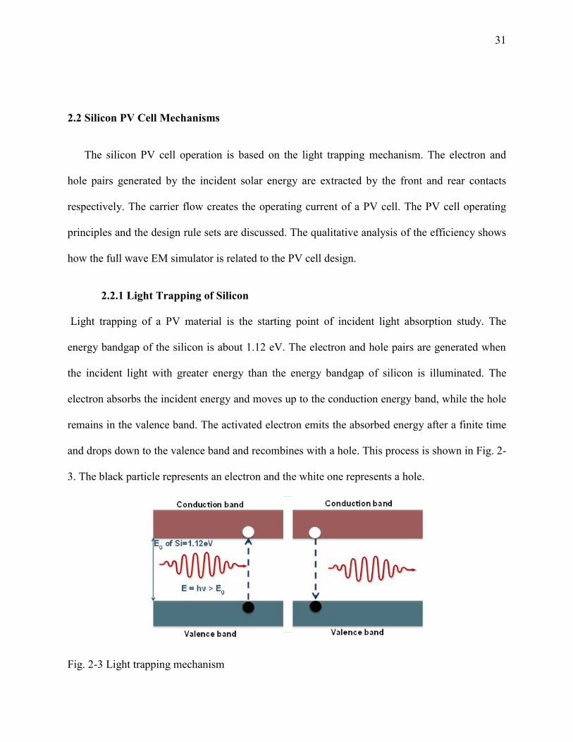
2.2 Silicon PV Cell Mechanisms
The silicon PV cell operation is based on the light trapping mechanism. The electron and
hole pairs generated by the incident solar energy are extracted by the front and rear contacts
respectively. The carrier flow creates the operating current of a PV cell. The PV cell operating
principles and the design rule sets are discussed. The qualitative analysis of the efficiency shows
how the full wave EM simulator is related to the PV cell design.
2.2.1 Light Trapping of Silicon
Light trapping of a PV material is the starting point of incident light absorption study. The
energy bandgap of the silicon is about 1.12 eV. The electron and hole pairs are generated when
the incident light with greater energy than the energy bandgap of silicon is illuminated. The
electron absorbs the incident energy and moves up to the conduction energy band, while the hole
remains in the valence band. The activated electron emits the absorbed energy after a finite time
and drops down to the valence band and recombines with a hole. This process is shown in Fig. 2-
3. The black particle represents an electron and the white one represents a hole.
Fig. 2-3 Light trapping mechanism

32
(a) (b)
(c) (d)
Fig. 2-4 Solar wave spectrums (a) at AM1.5 (b) along to wavelength (c) along to photon energy
(d) along to frequency
Solar irradiance spectrum in terms of wavelength, photon energy, and frequency are shown
in Fig. 2-3 [23]. The solar irradiance spectrum, the power of incident solar wave on the unit
surface, is measured with AM 1.5 that is the reciprocal cosine of incident angle between the
surface and solar wave. The solar irradiance with greater incident energy than the energy
bandgap of the silicon is the wavelength interesting range. The equations of photon energy and
frequency conversions from wavelength are
1 1.5 2 2.5 3 3.5 4 4.50
0.5
1
1.5
Photon energy, eV
So
lar
irra
dia
nce
, W
*m-2
*nm
-1
300 400 500 600 700 800 900 10000
0.5
1
1.5
Frequency, THz
So
lar
irra
dia
nc
e,
W*m
-2*n
m-1

33
Photon energy = hc/λ (2.1)
Frequency = c/ λ (2.2)
With h= 4.135667516e-15 eV∙s, and c=3e8 m/s.
Therefore, the frequency interest range is from 300 THz to 1000 THz according to (2.1) and
(2.2).
2.2.2 Flat Silicon PV Operation
The silicon PV operation principle is based on the light trapping mechanism, minority carrier
diffusion length of electron, and silicon doping. The silicon doping is a critical method to modify
the characteristics of intrinsic silicon. The n-type silicon is doped by elements impurities with
extra electrons, while the p-type silicon is doped with holes. The elements impurities with extra
electrons and holes are called donor and accepter, respectively. Flat silicon PV cells consist of
anti-reflection coating, front contact, n-type silicon, p-type silicon, and rear contact, as shown in
Fig.2-5. The total thickness of the substrate is greater or equal to 300 μm for higher absorption
with longer optical path length (OPL). The electron and hole pairs are generated by the incident
light around the depletion region due to the light trapping mechanism. The electron, a minority
carrier in p-type silicon layer, is extracted to the n-type silicon layer by the electric field flowing
from the n-type silicon layer to the p-type layer in the depletion region. The front contact and the
rear contact are fabricated on the front and back of silicon surface to lower high resistivity of
silicon substrate. The contacts are transparent, but electrically conductive. The electron is
collected by the front contact and reaches at the rear contact through the load. The electron is

34
recombined with a hole at the rear contact. The movement of electron creates the current flow of
the PV.
Fig. 2-5 Flat Silicon PV cell structure
2.2.3 Silicon PV Design Parameters
The appropriate size of p-n junction of the silicon PV is determined by minority carrier
diffusion length and depletion width. The thickness of the PV must be long enough to have
depletion region width at the boundary of p-type and n-type substrate. The thicknesses of n-type
and p-type substrates must be shorter than the minority carrier diffusion length of hole and
electron respectively as explained in the previous section. Determining doping density is
preceded because both depletion region width and minority carrier diffusion length are related to
the doping density.
The depletion region is created between n-type and p-type layers boundary region. Different
Fermi-levels at the junction interface collapses the equilibrium state and diffusion current flows
to restore the equilibrium state [24]. The depletion region is generated at the p-n junction after

35
electrons and holes at the junction are combined. Remained charges in the n-type layer and p-
type layer create built-in potential repelling the diffusion current. Minority carriers generated by
incident solar energy transport into another layer with the electric field created by the built-in
potential. This procedure is shown in Fig. 2-6.
(a)
(b)
Fig. 2-6 P-N junction (a) non-equilibrium state (b) equilibrium state
The diffusion coefficient of the minority carrier D is related to the minority carrier mobility
μ. The minority carrier lifetime τ is proportional to the doping concentration because more
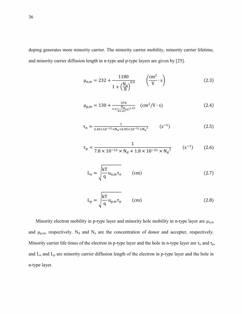
36
doping generates more minority carrier. The minority carrier mobility, minority carrier lifetime,
and minority carrier diffusion length in n-type and p-type layers are given by [25].
(
) (
)
√
√
Minority electron mobility in p-type layer and minority hole mobility in n-type layer are µn,m
and µp,m, respectively. Nd and Na are the concentration of donor and accepter, respectively.
Minority carrier life times of the electron in p-type layer and the hole in n-type layer are τn and τp,
and Ln and Lp are minority carrier diffusion length of the electron in p-type layer and the hole in
n-type layer.

37
The depletion width is inversely proportional to the doping concentration [24]. Let’s assume
that n-type doping concentration is higher than p-type doping concentration. Higher doping
concentration in n-type layer results in longer diffusion length of electron and wider depletion
width in p-type layer. In contrast, lower doping concentration in p-type layer generates narrower
depletion width in n-type layer. The equation of depletion width, depletion width in n-type layer,
and depletion width in p-type layer are
√
where Wd is depletion width, xn is depletion width in n-type layer, and xp is depletion width in
p-type layer [25].
The resistivity of the substrate is an important factor to determine the doping concentration
because low resistivity is preferred in design. Resistivity is related to the majority carrier
mobility and doping concentration. The related equations are below [25].
(
)

38
(
)
Resistivity is ρ, and µn and µp are majority electron mobility and majority hole mobility,
respectively.
2.2.4 Flat Silicon PV Efficiency
The solar efficiency is related to the number of incident photon, the electron and the hole pair
generation, and the electron extraction as described in Section 2.2.2. The solar efficiency can be
written as below.
where ηα is the optical absorption efficiency, ηg is the carrier generation efficiency, and ηext is the
electron extraction efficiency. The value ηα is related to the dielectric constant (ϵr) of the
substrate with sufficient optical path length (OPL). The reflection coefficient of a specific
material at an air interface in in terms of ϵr with the assumption of orthogonal incident solar wave
is shown below.
| √
√
| |
|
where Zair and Zsi are the intrinsic wave impedances of the air and the silicon and ϵr,si is a
dielectric constant of the silicon. The value of Zair is 377 Ω and ηsi is √ [26]. For example,

39
the reflection coefficient Γ between a silicon substrate and air is 0.55 if the dielectric constant of
the silicon ϵr,si is 11.9. The reflection coefficient Γ is inversely proportional to the optical
absorption efficiency ηα. The value of Γ is valid with sufficient OPL since a short OPL increases
reflection of the material. Because the intrinsic wave impedance is | | | |, the relationship
between ηα and Zsi shifts the viewpoint of a study from the material electronics focusing on the
electron and the hole behaviors to the electromagnetism with the field analysis on the substrate.
Therefore, the full wave EM simulators are applicable to the PV cell design.
In this dissertation, ηα and ηext are focused to enhance the total absorption efficiency of solar
cell substrate. The nanowire (NW) and branched nanowire (BNW) silicon PV with improved ηα
and ηext are discussed in Section 2.4. The full wave EM simulator modelings of NW and BNW
are introduced in Section 2.5.
2.3 Silicon PV Cell Parameters as a Circuit System
The PV cell parameters are quantified in terms of the power circuit. The external quantum
efficiency (EQE) is used to measure the efficiency of a PV cell. The output voltage of the PV
cell is logarithmically related to the operating current. The product of the output voltage and
operating current creates a power output. The IV curve shows the fill factor (FF) that is used to
calculate the PV cell efficiency. In this section, the PV cell parameters are introduced.
2.3.1 External Quantum Efficiency

40
The EQE is defined as the ratio of the number of charge carriers extracted by the solar cell
to the number of incident photons of the incident solar wave [27]. The higher value of EQE
corresponds to the more current flowing. EQE is a function of wavelength because the number of
extracted electrons and incident photons are wavelength dependent. The equation of EQE and the
maximum and minimum values of EQE over the wavelength interest are below.
where ne(λ) is the number of extracted electrons and np(λ) is the number of incident photons. The
greater EQE means the higher value of current generation with the given incident energy. The
EQE of typical silicon PV cell is shown in Fig. 2-7. The actual silicon substrate has smaller EQE
than the ideal EQE due to the recombination of minority carriers. The values of EQE at short and
long wavelengths are small because the short wavelengths are absorbed by the front surface
recombination while the long wavelengths are absorbed by the rear surface recombination. The
waves in the medium range of wavelength penetrate the front surface and are absorbed by the
bulk of the silicon. The maximum and minimum values of the actual EQE in the wavelength of
interest are 93.4 % and 43.1 %, respectively.

41
Fig. 2-7 External Quantum Efficiency
2.3.2 Silicon PV Fill Factor and Efficiency
The current created from the electron and hole pair is shown in Fig. 2-5. The short circuit
current flows when the front surface is connected to the rear surface. The short circuit current
density, Jsc is determined by the EQE and the incident photon flux density as shown below.
∫
where q is a charge of an electron. The PV cell is in the equilibrium state in the dark condition
and starts to operate once photons are incident to the front surface. The value of the current is
reduced when the load is connected at the terminal. There is a reverse current flowing created by
the output voltage at the load. The reverse current is called a dark current. The equivalent circuit
300 400 500 600 700 800 900 1000 1100 12000
10
20
30
40
50
60
70
80
90
100
Wavelength, nm
Exte
rnal Q
uan
tum
Eff
icie
ncy, %
Silicon EQE
Ideal EQE

42
of an ideal PV cell is shown in Fig. 2-8. The equation of ideal dark current density and load
current density are
( )
( )
where Jo is a reverse saturation current density, kB is the Boltzmann’s constant, T is the
temperature, and V is the output voltage.
The open circuit voltage is defined as the output voltage with an infinite load. The open
circuit voltage exists when there is no current flowing into the load, Jsc=Jdark. Therefore, the
equation of open circuit voltage is
(
)
Fig. 2-8 Equivalent circuit of an ideal PV cell
JSCJdark
-
+
Vout

43
The IV curve of a generalized PV cell is shown in Fig. 2-9. The relationship between the
current and voltage are shown with the power plot. Vmpp and Impp are the voltage and current
points resulting in the maximum power point. The fill factor (FF) is defined as a ratio of the
maximum power point (mpp) to the product of the ISC and VOC. The ideal value of FF is 1.
The efficiency of a solar cell is defined as the ratio of the maximum power point to the input
power. The equation of the PV efficiency is
Fig.2-9 IV curve of general PV cell
Impp
VOC
ISC
Curr
en
t (I
)
Voltage (V)
22
Vmpp
22Pmpp

44
2.4 Current State of Art on Nanostructured Silicon PV
2.4.1 Current State of Art
Nanoscale materials yield many benefits when used in PV and photoelectrochemical devices.
High performance nanomaterials enhance PV conversion efficiencies with potentially lower
material cost because either less material is needed or less expensive materials can be used.
Nanostructured PV materials that range from black silicon to NW to BNW as shown in Fig. 2-10
have been shown to have exceptional light trapping phenomena compared to conventional flat
surface topologies [28-30].
In conventional Si planar devices, for example, thick (>100 μm) high purity single-crystal Si
is required in order to maximize absorption of the incident solar radiation and achieve
sufficiently long minority carrier diffusion lengths (Ln). The result is that a large portion of the
cost of producing a crystalline Si PV module is associated with the production costs of the Si
wafers [31].
(a) (b) (c)
Fig. 2-10 Evolution of nanostructured Si solar cells (a) black silicon (b) NW (c) BNW
[1] [2] [3]

45
(a) (b)
Fig. 2-11 Optical path length of (a) Flat substrate (b) Black silicon substrate
The black silicon is a pyramid-shape silicon surface structure generated by the surface
texturization. The structure yields higher absorption of the incident solar wave than the flat
silicon PV. The texturized silicon surface yields longer OPL of the incident light by causing
refraction with the finite value of an incident angle at the surface. It is shown in Fig. 2-11. The
black silicon substrate still has low ηex because of the silicon substrate thickness for long OPL.
NW and BNW are new technology to solve the problem of low electron extraction efficiency.
NW solar cells allow the use of less expensive materials with higher level of impurities and
crystalline defects due to its high absorption of the incident light [32]. NW arrays for PV
applications can achieve high absorption efficiency over a broad range of wavelengths and
angles of incidence. The works in [32][33] shows solar cells with a NW p-n junction obtains
both good optical absorption and short collection lengths to provide large improvements in
efficiency. The NW with high aspect ratio, long height and short diameter, yields long OPL that
Flat substrate Black silicon substrate

46
improves the optical absorption efficiency (ηα). Additional work also shows radial p-n junction
Si NW arrays where the NW length is long to maximize solar absorption while maintaining a
short junction length, comparable to the NW diameter, to enable efficient carrier extraction (ηext)
[34]. The work in [35] shows significant improvements in overall efficiency. The entire design of
Si NW arrays can be optimized to achieve peak external quantum efficiency of 0.89 using the
radial p-n junction, using only a 1/100th
of the material of planar Si cells. The p-n junction in this
case is radial as shown in Fig. 2-12 (a). Maximizing efficiency requires that the wire array
provide high absorption and be sized for efficient carrier extraction.
Some recent focus on the light trapping aspects of Si NW have shown that there are various
design factors that enhance light trapping [36-40]. The first research in Si NW cells assumes that
light is incident from the end of the NW and thus trapped inside the NW. Subsequent research
showed significant absorption in NW arrays where the absorption increases at steeper angles of
incidence. This result provides a strong motivation to expect high efficiency from BNW
structures where some of the NW grow vertically and some NW grow horizontally to be able to
absorb light from a broad range of angles and solar wavelengths as shown in Fig. 2-12 (b). The
branches can serve as optical antennas and can significantly improve light harvesting in NW
array structures by providing more material per unit volume for light absorption and by
enhancing the scattering of light within the nanostructured surface which increases the effective
optical path length for light absorption [40].

47
(a) (b)
Fig. 2-12 PV cell structures of (a) NW (b) BNW
A number of studies have previously examined optical absorption in Si NW arrays. Some of
prior research in light absorption has been done experimentally. Most notably, a modeling study
in [41] demonstrated that Si NW arrays with a moderate filling factor have higher optical
absorption than a Si thin film of comparable thickness in the high-frequency regime but exhibit
reduced absorption at low frequencies due to a higher transmittance resulting from the small
extinction coefficient of Si. However, absorption in the low-frequency regime in Si NW arrays
can be significantly improved by employing light-trapping techniques.
48
2.4.2 NW and BNW Fabrication
The vapor-liquid-solid (VLS) growth method is one of the representative methods to
fabricate BNW surfaces with well-controlled branch diameter, size and angle [42]. The VLS
process involves the use of metal particles, most typically gold, which forms a liquid eutectic
phase with Si at low temperatures (~360oC for Au-Si) [42]. Once the liquid becomes
supersaturated with Si, crystalline Si precipitates in the form of a wire whose diameter is
controlled by the size of the initial metal particle. Consequently, the VLS technique provides a
bottom-up fabrication route to form high density arrays of Si BNWs with well controlled wire
diameters and lengths.
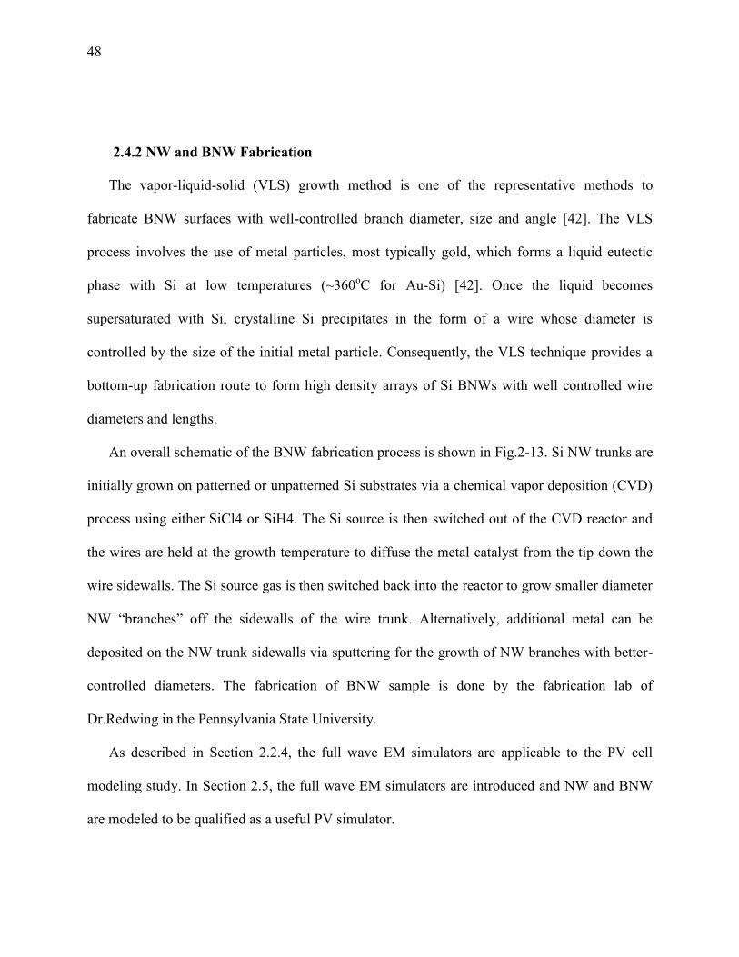
An overall schematic of the BNW fabrication process is shown in Fig.2-13. Si NW trunks are
initially grown on patterned or unpatterned Si substrates via a chemical vapor deposition (CVD)
process using either SiCl4 or SiH4. The Si source is then switched out of the CVD reactor and
the wires are held at the growth temperature to diffuse the metal catalyst from the tip down the
wire sidewalls. The Si source gas is then switched back into the reactor to grow smaller diameter
NW “branches” off the sidewalls of the wire trunk. Alternatively, additional metal can be
deposited on the NW trunk sidewalls via sputtering for the growth of NW branches with better-
controlled diameters. The fabrication of BNW sample is done by the fabrication lab of
Dr.Redwing in the Pennsylvania State University.
As described in Section 2.2.4, the full wave EM simulators are applicable to the PV cell
modeling study. In Section 2.5, the full wave EM simulators are introduced and NW and BNW
are modeled to be qualified as a useful PV simulator.

49
(a) (b)
(c) (d)
Fig. 2-13 Schematic of BNW fabrication process (a) patterned substrate (b) VLS growth of Si
NW trunks (c) metal diffusion or deposition (d) VLS growth of Si NW branches
2.5 Electromagnetic Computational Design for PV with Silicon Branch NW
The full wave EM simulators support the results from the solutions of Maxwell’s equations
without any simplifying assumptions. The Maxwell’s equations are solved with the dimensions
and material characteristics of the structures and the boundary conditions. The full wave EM
simulators are applied to the silicon NW and BNW PV design and the accuracy of the results is
discussed in this chapter.
2.5.1 Maxwell’s Equations and Boundary Conditions
The EM waves with a specific resonant frequency yielding reflectivity, absorption, and
transmission generated by electric and magnetic field, charge, and currents are calculated by
Maxwell’s equations. The finite Differential Time Domain (FDTD) method and Finite Element
Method (FEM) are two representative EM computational simulation methods using Maxwell’s
equation. Time harmonic Maxwell’s equation is shown in Table 2-1 [43].
SiCl4/SiH4

50
Table 2-1 Time Harmonic Maxwell’s equation
The quantities are defined as follows:
is the electric field intensity (V/m).
is the magnetic field intensity, (V/m).
is the electric flux density, (Coulombs/m2).
is the magnetic flux density (Webers/m2).
is the source electric current density (A/m2).
is the conduction electric current density (A/m2).
is the source magnetic current density (V/m
2).
is electric charge density (Coulombs/m2).
is electric charge density, (Webers/m2).
The wave equations of an EM wave propagating in a material are derived from the
differential form of the Maxwell’s equations and are continuous in terms of electrical properties.

51
Boundary conditions are applied to solve the partial differential equations (PDE) of the
Maxwell’s equation at the interface of two different media. The PDEs of the boundary conditions
on the entire fields for general cases are shown below.
The full wave EM simulators analyze the structures based on the dimensions, the material
characteristics, and the boundary conditions. The proper boundary conditions on the surfaces of
the structures bring accurate simulation results.
2.5.2 Full Wave EM Modeling Computational Simulation Tools
An excellent qualitative review of the EM computational simulation tools for nanowire (NW)
solar cells using Finite Difference Time Domain (FDTD) and Finite Element Method (FEM) is
provided in [44]. FDTD generates electric and magnetic equations in the unit lattice that is called
Yee’s lattice with tensorial grid by using finite difference method. Boundary conditions and
material characteristics determine the truncation condition and generate the incident wave
condition. The initial electric and magnetic fields are calculated based on the incident wave
condition and yield all electric and magnetic fields by time increment. This process is shown in
Fig. 2-14.
52
(a) (b)
Fig. 2-14 FDTD method (a) FDTD process (b) Yee’s lattice
FDTD requires external plotting tools and the structure image software because it has only
analysis function of structure. FDTD produces .dat file and .h5 file that are used for the structure
diagram view and result plots. Matlab and h5utils are used for results plotting and diagram
generation. A study in [45] used MIT electromagnetic equation propagation (MEEP), which is
one of FDTD tool, for the analysis of Si BNW structures.
FEM divides the unit structure into tetrahedrons which is called meshes, to calculate
Maxwell’s equations at the points and edges of the meshes. There is no limit of structure shape
because meshes can be generated from any structures. The initial meshes are generated based on
the solution frequency set by users and a parameter representing R, A, and T of the initial meshes,
S, is calculated. This process is repeated with new meshes divided from the initial meshes until
the difference between the values of S from two passes are smaller than Δ S determined by users.
Maxwell’s equations
E and H equations in cellBoundary condition and
material characteristics
Time increment
Finite difference method
Truncation condition
Initial E and H fields
Incident wave condition
All E and H fields

53
When this loop is over, plots are generated based on the values of S. The FEM algorithm is
shown in Fig. 2-15. The implementation of high frequency structure simulator (HFSS)
simulation that is a representative FEM tool for the flat PV is shown in [46]. Silicon BNW PV
cells design with MEEP and HFSS are compared through quantitative results of reflection and
absorption.
(a) (b)
Fig. 2-15 FEM (a) Analysis Algorithm (b) Meshes
2.5.3 MEEP and HFSS Verification
The NW PV is an array with infinite number of regularly spaced nanotree. Modeling of
whole dimension of NW PV cell is an electrically large structure that is time consuming and
extremely expensive. A rectangular waveguide provides the behavior of an infinite periodic
structure with the symmetry of a unit cell [47]. The traditional rectangular waveguide suggests a
rectangular boundary of perfect electric conductor (PEC) walls around the unit cell. The image
effect of the PEC creates image structures around the walls as an object inside a room of mirrors
Adaptive initial Mesh Generation
Calculation of S from
the initial mesh
Additional mesh
generation and
calculation new
S-parameters
Calculation of ∆s
and comparing
to default ∆s
Finishing the mesh generation
Plotting based on the S-parameters
∆s>default ∆s
∆s<default ∆s

54
on the four side walls. The images on the parallel to the direction of the electrical current
structure have the opposite direction from the original structure if the object is asymmetrical as
shown in Fig.2-16 (a). The full wave EM simulators are able to use perfect magnetic conductor
(PMC) walls for the radiation cell [48]. The images parallel to the original structure with PMC
walls have the same direction as the structure resulting in all in-phase replicated arrays.
Therefore, the current rectangular waveguide has the PEC and PMC walls on the surfaces
perpendicular to the E field and the H field as shown in Fig.2-16 (b).
The absorbing boundary condition (ABC) is assigned on the top of unit cell to result in the
infinite boundary condition. The ABC absorbs al EM field inside the unit cell to create infinite
boundary. The full wave EM simulators have their own boundary conditions to be used for the
periodic structure, but the basic principles agree to the ABC, PEC, and PMC boundaries. The
perfectly matched layer (PML) at the top and bottom of the unit cell plays a role of ABC in
MEEP. The “Periodic Boundary Condition” of MEEP repeats all E and H fields inside the unit
cell along to the given direction. Therefore, periodic boundary of MEEP has two PMLs at the top
and bottom of the unit cell and assign “Periodic Boundary Condition” with the direction of the
unit cell dimension.
(a) (b)
Fig. 2-16 Effect of rectangular waveguide (a) traditional method (b) current method
PEC wall
PMC wallUnit cell orientation
PEC wall
PMC wallUnit cell orientation

55
HFSS has unique periodic boundary condition, which is M/S boundary with Floquet port
M/S boundary of HFSS has the same function as the “Periodic Boundary Condition” of MEEP,
replicating all E and H fields in the unit cell. Floquet ports at the top and bottom of the unit cell
are the input port and output port respectively, and have a great absorption of the incident EM
wave [49]. The work of [45] verifies MEEP by modeling a structure from [41] and comparing
the results.
The authors in [41] used the transfer matrix method (TMM) to compare the flat silicon PV
film and NW PV surface. The thickness of PV film is 2.33 µm, and lengths of NWs are 1.16 µm,
2.33 µm, and 4.66 µm, respectively. The height of 2.33 µm is 5.8 λ with 750 THz frequency.
MEEP and HFSS NW PV unit cell with periodic structures are shown in Fig. 2-17. HFSS used to
show 3D MEEP design because MEEP does not offer 3D graphic user interface (GUI).
Fig. 2-17 NW PV unit cell with periodic structures
ABC
2.33 µm
= 5.8 λ
PEC
PEC
PMC
PMC
=
1 µm 1 µm

56
(a) (b)
(c) (d)
(e) (f)
Fig.2-18 Absorption comparisons of NWs with 1.16 µm, 2.33 µm, and 4.66 µm and film, and
reflection and transmittance comparisons of NWs with 2.33 µm and film (a) absorption from
TMM [37] (b) reflection and transmittance from TMM [37] (c) absorption from MEEP (d)
reflection and transmittance from MEEP (e) absorption from HFSS (f) reflection and
transmittance from HFSS
1 2 3 40
20
40
60
80
100
Photon Energy, eV
% R
efl
ecti
on
an
d T
ran
sm
itta
nce
Reflection, 2.33 umReflection, Film(2.33 um)Transmittance, 2.33 umTransmittance, Film(2.33 um)
1 2 3 40
20
40
60
80
100
Photon Energy, eV
% A
bso
rp
tio
n
4.66 um2.33 um1.16 umFilm(2.33 um)
1 2 3 40
20
40
60
80
100
Photon Energy, eV
% R
efl
ecti
on
an
d T
ran
sm
itta
nce
1 2 3 40
20
40
60
80
100
Photon Energy, eV
% A
bso
rp
tio
n

57
MEEP simulation results and HFSS simulation results with the flat film and different lengths
of NWs are shown in Fig.2-18. MEEP and HFSS can be used for modeling PV substrate because
the results are well matched to the results from the TMM in the reference. The simulation results
from MEEP and HFSS are well-matched to each other, but still show small mismatches. The
difference between MEEP and HFSS results are caused by the different characteristics of the
boundary conditions from MEEP and HFSS. The ABC layer of HFSS has stronger absorption
than MEEP.
The time and memory usage of MEEP and HFSS are shown in Fig 2-19. The time usage of
MEEP and HFSS are similar to each other, but memory usage of HFSS is much greater than one
of MEEP. It is reasonable because FEM requires a lot of memory to generate meshes and to
analyze them, while FDTD uses memory to calculate Maxwell’s equations with finite difference
method and boundary conditions.
(a) (b)
Fig. 2-19 (a)The time usage of MEEP and HFSS and (b) memory usage of MEEP and HFSS
0
50
100
150
200
250
400 500 600 700 800 Total
Tim
e ,
se
c
Wavelength, nm
HFSS
MEEP
0.01
0.1
1
10
100
1000
MEEP HFSS
Me
mo
ry,
MB

58
2.5.4 MEEP and HFSS BNW Design Comparison
The results of BNW PV modeling with radial p-n junction, with the p-type c-Si and n-type
a-Si:H from MEEP and HFSS are compared. The values of n-type and n-type BNW radius was
determine by the equations from Section 2.2.4. The doping of n-type silicon and p-type silicon
which generate the smallest resistivity are selected. The doping concentrations from 1x10¹⁶
cm-3
to 1x10¹⁹
cm-3
ranges are practically calculated and 5x10¹⁸
cm-3
is selected as the p-type doping
concentration. The resistivity of p-type c-Si is about 0.015 Ω/cm. The resistivity of n-type a-Si:H
is about 100 Ω/cm with 1.5x10¹⁸
cm-3
doping concentration because the mobility of a-Si:H is 100
to 1000 times less than the one of c-Si [50].
The depletion width in p-type layer has about 10 nm and the minority carrier diffusion
length of electron is about 5.9x10³ nm. The difference between radius of n-type NW and p-type
NW should be greater than the depletion width in n-type layer, about 0.9 nm. Therefore, the
radius of n-type NW and p-type NW are determined which satisfy the conditions above with the
highest efficiency.
The BNW has 10 µm heights, which is 25 λ with 750 THz frequency, 0.12 µm of outer
radius, 0.096 um of inner radius, 0.5 µm of branch length, 0.06 µm of outer branch radius, 0.048
µm of inner branch radius, 1 µm of branch spacing, and 9 branches. The design parameters of the
BNW is shown in Table 2-2. The BNW unit cell and periodic boundary condition of MEEP and
HFSS are shown in Fig. 2-20. The BNW modeling results of absorptions and reflections from
MEEP and HFSS are shown in Fig. 2-21. They are well matched, so MEEP and HFSS can be
used for BNW PV modeling.
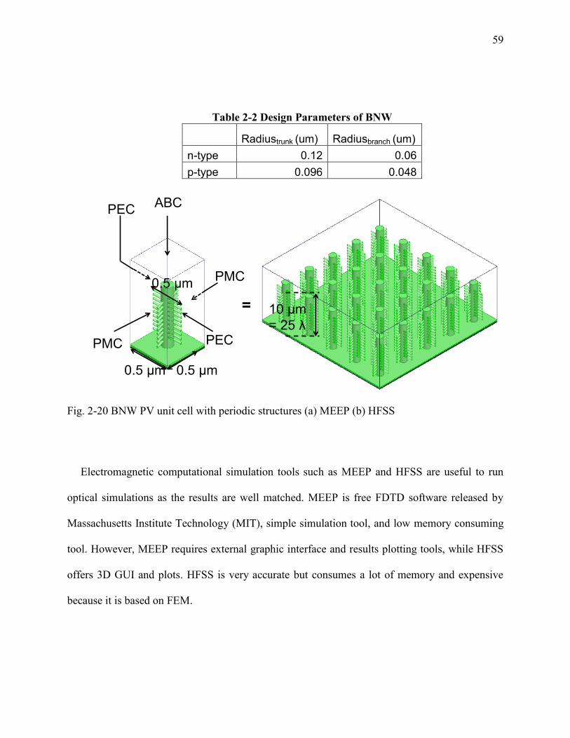
59
Table 2-2 Design Parameters of BNW
Radiustrunk (um) Radiusbranch (um)
n-type 0.12 0.06
p-type 0.096 0.048
Fig. 2-20 BNW PV unit cell with periodic structures (a) MEEP (b) HFSS
Electromagnetic computational simulation tools such as MEEP and HFSS are useful to run
optical simulations as the results are well matched. MEEP is free FDTD software released by
Massachusetts Institute Technology (MIT), simple simulation tool, and low memory consuming
tool. However, MEEP requires external graphic interface and results plotting tools, while HFSS
offers 3D GUI and plots. HFSS is very accurate but consumes a lot of memory and expensive
because it is based on FEM.
PMC
ABCPEC
PEC
PMC
10 µm
= 25 λ
=
0.5 µm 0.5 µm
0.5 µm
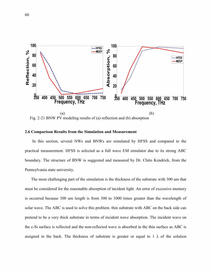
60
(a) (b)
Fig. 2-21 BNW PV modeling results of (a) reflection and (b) absorption
2.6 Comparison Results from the Simulation and Measurement
In this section, several NWs and BNWs are simulated by HFSS and compared to the
practical measurement. HFSS is selected as a full wave EM simulator due to its strong ABC
boundary. The structure of BNW is suggested and measured by Dr. Chito Kendrick, from the
Pennsylvania state university.
The most challenging part of the simulation is the thickness of the substrate with 300 um that
must be considered for the reasonable absorption of incident light. An error of excessive memory
is occurred because 300 um length is from 300 to 1000 times greater than the wavelength of
solar wave. The ABC is used to solve this problem. thin substrate with ABC on the back side can
pretend to be a very thick substrate in terms of incident wave absorption. The incident wave on
the c-Si surface is reflected and the non-reflected wave is absorbed in the thin surface as ABC is
assigned in the back. The thickness of substrate is greater or equal to 1 λ of the solution
350 400 450 500 550 600 650 700 7500
20
40
60
80
100
Frequency, THz
Re
fle
cti
on
, %
HFSSMEEP
350 400 450 500 550 600 650 700 7500
20
40
60
80
100
Frequency, THzA
bs
orp
tio
n, %
HFSSMEEP

61
frequency to have the absorption of one wavelength. The HFSS model of c-Si substrate with the
ABC boundary is shown in Fig. 2-22.
Fig. 2-22 Thin substrate with ABC approximation to the thick substrate
The reflectivity of normal incident light is calculated by the equation below.
where Zc-Si and Zair are the intrinsic wave impedance of c-Si and air, respectively. The
reflectivity from HFSS simulation is compared to the calculated reflectivity and measured value
from Dr.Kendrick. It is shown in Fig. 2-23. The values of reflectivity from three different
methods are well matched to each other. This shows that the thin c-Si substrate with ABC can
play a role of 300 um thick c-Si substrate.
Absolute
boundary
condition
≥λ
Air
c-Si
300 um
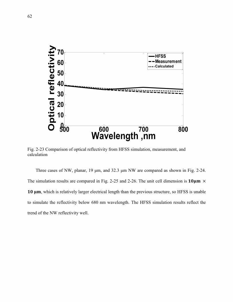
62
Fig. 2-23 Comparison of optical reflectivity from HFSS simulation, measurement, and
calculation
Three cases of NW, planar, 19 μm, and 32.3 μm NW are compared as shown in Fig. 2-24.
The simulation results are compared in Fig. 2-25 and 2-26. The unit cell dimension is
, which is relatively larger electrical length than the previous structure, so HFSS is unable
to simulate the reflectivity below 680 nm wavelength. The HFSS simulation results reflect the
trend of the NW reflectivity well.
500 600 700 8000
10
20
30
40
50
60
70
Wavelength ,nm
Op
tic
al
refl
ecti
vit
y ,
%
HFSSMeasurementCalcualtedCalculated

63
(a) (b) (c)
Fig. 2-24 Unit Cell of NW structures (a) planar (b) 19 μm (c) 32.3 μm
Fig. 2-25 Optical reflections of three different NW lengths from HFSS simulation
10 µm 10 µm0.8 µm
19 µm
10 µm 10 µm
Planar 19 µm NW
32.3 µm
10 µm 10 µm
32.3 µm NW
680 700 720 740 760 780 8000
10
20
30
40
50
60
70
Wavelength ,nm
Op
tical
refl
ecti
vit
y ,
%
Planar
19 um
32.3 um

64
Fig. 2-26 Optical reflections of three different NW lengths from measurement
For BNW design, the height and radius of trunk are 32.3 µm and 0.9 µm, respectively. The
spacing of the branches is 2 µm. The radius of branch is fixed as 0.075 µm. Another considerable
factor is the direction of branches. The direction of branch can go upward or downward, and it
affects on the reflection of the BNW. Upward direction of branch has 65˚ angle between the top
of trunk and branches, while there is 115˚ between the trunk and downward branches. There are
three different cases of branch direction: 100 % upward, 0 % upward, and 50 % upward. The
case of 100% upward means all branches have upward direction, while 0% means all branches
have downward direction. In the case of 50 % upward, the branch lines in each face of hexagonal
alternately have different directions alternatively. If one face has upward direction, the neighbor
faces have downward directions. Fifty % upward direction is selected for the simulation. A pure
680 700 720 740 760 780 8000
10
20
30
40
50
60
70
Wavelength, nm
Op
tical
refl
ecti
vit
y,
%
Planar
19 um
32.3 um

65
c-Si hexagon is used for the BNW instead of the p-n junction silicon cylinder for easier and
faster meshing.
The length of branch is a parametric factor of the simulation. The reflection of BNW with
longer branches is supposed to have less value of reflection because more dimension of branches
result in higher ηex. In this simulation, different lengths of branches are 1 µm, 3 µm, and 5 µm
lengths of branches as shown in Fig. 2-27.
The simulation results from different length of branches are compared to the reflectivity of
NW with the same height in Fig. 2-28. The results between 700 to 900 nm are shown because of
the memory limit. In most wavelengths, BNWs the longest length of branch have the smallest
reflection. The measurements of BNWs with 32.3 μm height and 0.9 μm radius NW with 0.075
µm radius and different length are shown in Fig. 2-29[51].
(a) (b) (c)
Fig. 2-27 Unit Cell of BNW structures with different branch lengths (a) 1 µm (b) 3 µm (c) 5 µm
32.3 µm
10 µm 10 µm
32.3 µm
10 µm 10 µm
32.3 µm
10 µm 10 µm

66
Fig. 2-28 Optical reflections of three different branch lengths from HFSS simulation
Fig. 2-29 Optical reflections of three different branch lengths from measurement
700 720 740 760 780 8000
10
20
30
40
50
60
70
Wavelength, nm
Op
tic
al
refl
ecti
vit
y,
%
Planar
Short (1 um)
Meadium (3 um)
Long (5 um)
700 720 740 760 780 8000
10
20
30
40
50
60
70
Wavelength, nm
Op
tic
al
refl
ecti
vit
y,
%
Planar
Length of Branch = 1 um
Length of Branch = 5 um
Length of Branch = 10 um
700 720 740 760 780 8000
10
20
30
40
50
60
70
Wavelength, nm
Op
tical
refl
ecti
vit
y,
%
Planar
Short (1 um)
Meadium (3 um)
Long (5 um)

67
The simulation results are not as well-correlated with the measurement results as the NW
results. The practical fabrication modeling has high irregularity in the direction, position, and
length of branches while HFSS has perfectly regular dimension of branches. The high
irregularity of the practical structure is the reason of the results mismatching. The HFSS models
and simulation result of different branch directions, 100 %, 50 %, and 0%, are shown in Fig. 2-
30 and 2-31, respectively. It shows that 100 % upward branch direction causes from 60 to 76 %
error of reflectivity from 50% and 0% upward branch directions. In conclusion, considering the
irregularity of the BNW design is a future work for better correlation of the full wave EM
simulation and practical measurement.
(a) (b) (c)
Fig. 2-30 Unit Cell of BNW structures with different branch directions (a) 100 % (b) 0 % (c) 50 %
32.3 µm
10 µm 10 µm
32.3 µm
10 µm 10 µm
32.3 µm
10 µm 10 µm
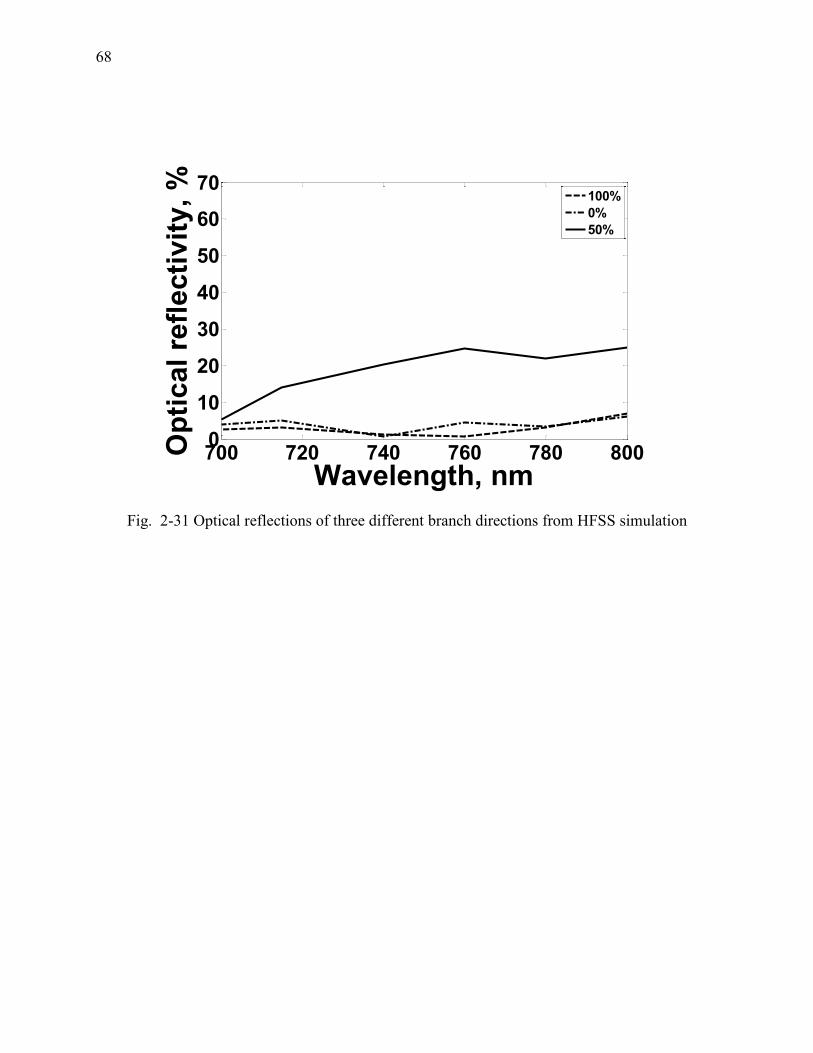
68
Fig. 2-31 Optical reflections of three different branch directions from HFSS simulation
700 720 740 760 780 8000
10
20
30
40
50
60
70
Wavelength, nm
Op
tic
al
refl
ecti
vit
y,
%
100%
0%
50%

69
CHAPTER 3 DESIGN OF 60-GHZ ANTENNA ARRAY FOR MULTI-CHIP
COMMUNICATION
3.1 Introduction
The development of the high performance computing (HPC) systems requires a processor
with higher clock speed [9]. The enhanced clock speed results in the increased central processing
unit (CPU) power dissipation [10]. The design of multi-chip multi-core (MCMC) system is a
promising processor because of the low CPU power dissipation. The MCMC consists of two or
more than individual CPU cores with the capabilities of read and execute. The performance of
processor is more enhanced and the less power is consumed than the single core processor as
each core runs independently at the same time. The multiple cores operating for the parallel
processing are integrated to build a single chip, in a module of the massive data cluster.
The cores in a chip communicate to each other for the I/O data transfer by the physical wire-
bonding. Wire-bonding is broadly used wire interconnect method because of the advantages in
cost and flexibility. However, wire-bonding is not appropriate method for interconnect between
the small chips. The existence of wire connection causes parasitic inductance affecting on the
data communication. The wire is located at the edge of the chips for the efficiency of chip
packaging. The rate of the I/O pitch size reduction is less than the rate of chip size reduction,
which causes the mutual coupling capacitance between adjacent wires.
A millimeter wireless link for the data communication system is investigated to solve the
problems of the I/O pitch scaling down and the crosstalk between adjacent wires. In the
suggested system, nine cores are connected with wire-bonding and on-chip antenna is fabricated
on the center core, a router. The router does the wireless communication with other routers in

70
neighbor group of cores. The low profile antenna operating at 60 GHz is selected for the 15% -10
dB reflection coefficient bandwidth, which enables about 20 Gbps data transfer [14]. The four
element array antenna design process, design results analysis, and the expected applications of
the reconfigurable on-chip antenna are discussed in this Chapter.
3.2 Current State of Art
The antenna for the wireless link is designed to transmit data to the horizontal direction with
enough bandwidth at 60 GHz. The antenna in package was selected for the candidate of the
MCMC antenna because it has benefits of the antenna efficiency over the antenna on chip [52].
Because high dielectric silicon chip located below the antenna dissipates propagating, the
antenna on chip has low efficiency. ground shielded metal and package on top of the antenna in
package prevent the energy dissipation and enhance wave propagation in the horizontal direction
[52][53]. An example of an aperture feed antenna in package profile is shown in Fig. 3-1 [54].
Fig. 3-1 Antenna in Package profile [54]
Patch
Antenna GND
Antenna Cavity
GND
RFIC
Antenna FeedGND Via

71
The low-profile antenna in package mounted on the ground plane generates an image current
source. The image current created by the perfect electric conductor (PEC) deteriorates the
original current source due to its opposite direction to the original antenna current source [43]. A
good solution for the image current effect is using perfect magnetic conductor (PMC) as the
ground plane that creates an identical directional image current source to the original antenna
current direction. An artificial magnetic conductor (AMC) that operates as a PMC at a specific
frequency is introduced [55].
The mushroom-like AMC layer consists of the dielectric substrate, periodic patches, and
vertical vias connecting the ground plane and patches as shown in Fig. 3-3 (a). The mushroom-
like structure creates a parallel resonant circuit with inductance and capacitance, which creates
very high impedance near the resonant frequency [56]. The high impedance surface prevents the
surface wave propagation at the resonant frequency, which is similar to the property of PMC
layer. However, the mushroom-like AMC structure is in appropriate as the ground plane of the
low profile antenna due to its two disadvantages. First, the suppressed surface wave declines
wave radiation from the antenna on the mushroom-like AMC layer [56][57]. Second, the vias
between the patches and ground plane make the fabrication process more difficult. Another kind
of AMC layer is needed to be introduced to solve these problems. A periodically-patched AMC
layer involves the dielectric substrate, the periodic patches and the ground plane as shown in Fig.
3-2 (b) [57]. The impedance of the AMC layer around the resonant frequency is reduced because
inductance from the vertical vias is removed. The surface wave in the AMC layer is created,
enhancing the dielectric wave propagation through the substrate. The periodically-patched AMC

72
is a simpler structure than the mushroom-like AMC layer structure because the vertical vias is
not fabricated.
(a) (b)
Fig. 3-2 Profiles of (a) mushroom-like AMC layer and (b) periodically-patched AMC layer
The reflection phase on the patch of mushroom-like AMC layer and periodically-patched
AMC operating at 60 GHz are shown in Fig. 3-3. Both the mushroom-like AMC layer and
periodically-patched AMC layer shows 0˚ reflection phase, which means the current source and
the image current are in phase around 60 GHz.
Fig. 3-3 Reflection phases of mushroom-like AMC and periodically-patched AMC layer
+ C -
L<
+ C -

73
Fig. 3-4 Design parameters of AMC layer
The first step of the design procedure of the AMC layer is to determine the size of the
periodic patches on the AMC layer. After the design of AMC layer is complete, the antenna is
designed based on an AMC that provides a reflection phase. The width of the patch, W, the
gap between the patches, g, and the substrate height, h, shown in Fig 3-4, determine the
reflection phase given plane wavepropagation toward the AMC layer.
The parameters W and g influence the capacitive behavior while h primarily influences the
inductive characteristics of the surface impedance. The table of dimension parameters from two
different materials is below, while W, g, and h are the width, gap, and height of the patch
[56][58]. They have the same values except the W and εr, which means that W is a function of εr.
Roger 3003 laminates [59] with εr= 3.1 and tanδ=0.002 was selected due to the stability of
dielectric constant over temperature and a low dissipation factor. The reflection phase of the
AMC layer is characterized using the rectangular waveguide simulator method in the finite
element analysis tool, HFSS [49]. The simulation setup in HFSS is presented in Fig. 3-5. The
waveguide simulator assumes a plane wave propagating at normal incidence in a unit cell with
perfect electric and perfect magnetic boundary conditions as shown in [48].
W
g
h
Patch
Ground

74
Table III-1 Dimension parameters of AMC layer
#Reference W g h εr
[56] 0.12λ 0.02λ 0.04λ 2.2
[58] 0.10λ 0.02λ 0.04λ 2.94
Fig. 3-5 Waveguide simulator setup to predict values of reflection phase
The HFSS simulation result of the reflection phase verses the frequency with different W
with h=0.25 mm and g= 0.12 mm is plotted in Fig.3-6 [14]. The values of h and g are fixed by
the manufacturer and fabrication vender, respectively. The value of W is determined as 0.58 mm
because W=0.58 mm results in the 0˚ reflection phase.
Plane Wave
ExcitationPMC
PMC
PEC
PEC

75
Fig. 3-6 Reflection phase of periodic-patch AMC layered ground plane
The antenna in package fabricated on the AMC layer is shown in Fig. 3-7. A single antenna
in package design on AMC layerfor MCMC system is introduced by Nobuki Hiramatsu and Ho-
hsin Yeh [14][60].
Fig. 3-7 Multi-chip multi-core system with wireless link antenna [14]
0.58mm
0.12mm0.4mm
1.1 mm
0.25 mm
0.13 mm
Antenna
Patch
Ground
Inner conductor
Silicon
RO3003

76
Fig. 3-8 Two element array antenna [61]
Stronger directivity of the antenna to the other router is required to improve the performance
of the wireless communication. Two element array on the AMC layer creating stronger
directivity was introduced in [61][62]. The substrate material used is a hydrocarbon ceramic type
laminate, Rogers 4003, which enables the copper-plated through hole generation [63]. The
chemical wetting process is not required before producing the copper-plated through hole vias.
The dielectric constant and tanδ are 3.55 and 0.0027 s/m, respectively. The dimensions of the
two element array on AMC layer is shown in Fig. 3-8 [61]. The gain of the antenna was
enhanced about 5 dBi in the horizontal direction. The overall diagram of multi-chip
communication system with two element array is shown below.

77
Fig. 3-9 Overall multi-chip communication system with two element array
(a) (b)
Fig. 3-10 (a) Simulated and measured performances on the reflection coefficient S11 (b)
measurement setup
50 52 54 56 58 60 62 64 66 68 70-35
-30
-25
-20
-15
-10
-5
0
Frequency (GHz)
Re
flectio
n C
oe
ffic
ien
t (d
B)
Simulation
Measurement
Probe Station Holder
Feeding Layer
Antenna Layer

78
Fig. 3-11 Wireless link communication system
The simulation performance of two element array comparison with reflection coefficient
measurement and the measurement setup along with the probe station are shown in Fig. 3-10
[61]. The reflection coefficient comparison plot shows well-matched input impedance at 60 GHz
with a reasonable -10 dB bandwidth.
The wireless link performance needs to be calculated to quantify the efficiency of antennas.
The wireless link communication system is shown in Fig. 3-11. The circuit of TX and RX
contain the amplifier circuits to recover the loss caused by the path link. The quantifying process
starts with the Friis equation showing the relationship between the antenna power, antenna gain,
and path loss due to the distance between antennas [62].
| |
| | (
)
In this equation, |S11|t = |S11|r and Gt = Gr if TX and RX are identical antennas. The
simplified equation is
| |
(
)
The dB scale of the equation (3.2) introduces a new antenna performance parameter as
shown below.
RXTX

79
( | | (
)
)
PRE is the power loss created by the wireless link path to be recovered by the amplifiers in
TX and RX circuits [13]. The lower value of PRE achieves the higher efficiency of wireless
system. Another quantity including the bandwidth of the antenna, budget, is introduced as
( | | (
)
)
The wireless system with low PRE and high bandwidth results in low budget. The value of
PRE is related to the gain of the antenna while the budget is influenced by the bandwidth. The
gain and the bandwidth of several antennas including single and two element array AMC
antennas are in Table 3-2 The PRE and Budget of the antennas in Table 3-2 are shown in Fig. 3-
12 [61][62]. A new antenna with lower PRE and Budget than the values in Fig. 3-12 is designed
in next section.
Table 3-2 Gain and bandwidth of current state of art
Reference Antenna Type Gain (dBi) Bandwidth (GHz)
[63] CMOS Yagi -8 10
[54] Off-Chip Bondwire -3.2 3
[65] Off-Chip Yagi 6 2
[14] Single AMC Antenna -0.5 13
[61] Two Array AMC Antenna 5 11

80
(a)
(b)
Fig. 3-12 Wireless link performance of current state of art comparison (a) power loss required to
be recovered (b) budget
10 12 14 16 18 20 22 24 26 28 300
5
1015
2025
3035
4045
5055
Transmission distance, mm
PR
E, d
B
CMOS Yagi
Off-Chip Bondwire
Off-Chip Yagi
Single AMC Antenna
Two array AMC antenna
10 12 14 16 18 20 22 24 26 28 300
2
4
6
8
10
12
14
16
18
20
Transmission distance, mm
Bu
dg
et,
dB
/GH
z
CMOS Yagi
Off-Chip Bondwire
Off-Chip Yagi
Single AMC Antenna
Two array AMC antenna

81
3.3 Reconfigurable four element array for MCMC system
The reconfigurable antennas are promising technology to extend the application of a single
antenna system in terms of the operating frequency and the radiation pattern. The antenna
reconfigurability of the operating frequency with constant radiation patterns are shown in [67]-
[69]. One of the pattern reconfigurable antenna is the smart antenna that is a phased array
antenna with antenna beamforming system [66]. The smart antenna is able to produce variable
radiation patterns. However, adding and developing the antenna beamforming system is
uneconomical. The pattern reconfigurable square spiral microstrip antenna is introduced, which
uses switched connections between antenna and additional parts, the shorting pin and opened line
[70]. The reconfigurable antenna with the radio frequency micro-electro-mechanical system (RF-
MEMS) is introduced in [71]. The switching antenna power in the array antenna is used for the
antenna reconfigurability in this dissertation.
Two element array restricts the possible communication directions into one way as shown in
Fig. 3-9. The router 1 has strong wireless communication with the router 4 but the wave
directivities to the router 2 and router 3 are small. A router is supposed to communicate to all
adjacent routers with strong and clear signal communication. The expected wireless
communication diagram is shown in Fig. 3-13. A single antenna might be enough to
communicate with the other four routers in orthogonal direction because the distance is shorter.
However, fabricating four pairs of two element array and four single antennas is detrimental
solution because of the fabricating cost and huge power consumption. An effective array-antenna
orientation resulting in optimized gain in all directions is required.

82
Fig. 3-13 Expected gain pattern of a router to the neighbor routers
The design considerations of the MCMC antenna are suggested in [14]: the chip integration,
the radiation pattern in the horizontal direction, and 15% 10 dB bandwidth over 60 GHz. In
addition, the PRE and Budget of the antenna must be lower than the existing antennas. The
reconfigurable four element array creates reasonable directions of radiation pattern by the
combinations of two antennas. The appropriate AMC layer design produces a horizontal
radiation pattern and broad bandwidth. The dimension of antennas determines resonant
frequency and matches input impedance. The direction and value of combined radiation pattern
from two antennas are influenced by the location of antennas, including the orientation and
distance between the antennas. In this dissertation, gain pattern is plotted to demonstrate the gain
and radiation pattern together. The expected gain pattern created by two antennas is shown in Fig.
3-14.
CORE
Router
CORE
CORE
CORE
CORE
CORE
CORE
CORE
CORE
Router
CORE
CORE
CORE
CORE
CORE
CORE
CORE
CORE
Router
CORE
CORE
CORE
CORE
CORE
CORE
CORE
CORE
Router
CORE
CORE
CORE
CORE
CORE
CORE
CORE
CORE
Router
CORE
CORE
CORE
CORE
CORE
CORE
CORE
CORE
Router
CORE
CORE
CORE
CORE
CORE
CORE
CORE
CORE
Router
CORE
CORE
CORE
CORE
CORE
CORE
CORE
CORE
Router
CORE
CORE
CORE
CORE
CORE
CORE
CORE
CORE
Router
CORE
CORE
CORE
CORE
CORE
CORE
CORE

83
Fig. 3-14 Gain pattern created from two identical antennas
The appropriate orientation of four antennas creates the wave propagation in eight directions.
The individual antennas are expected to create the orthogonal direction of data communication
while the two pairs of antenna are designed to produce the wave propagation to the routers in the
four diagonal corners. Two cases of antenna orientations, the ring shape and star shape four
antennas are suggested in Fig. 3-15. The antenna directivity is the direction of the maximum
intensity radiated.
(a) (b)
Fig. 3-15 Four antenna orientations (a) ring shape (b) star shape
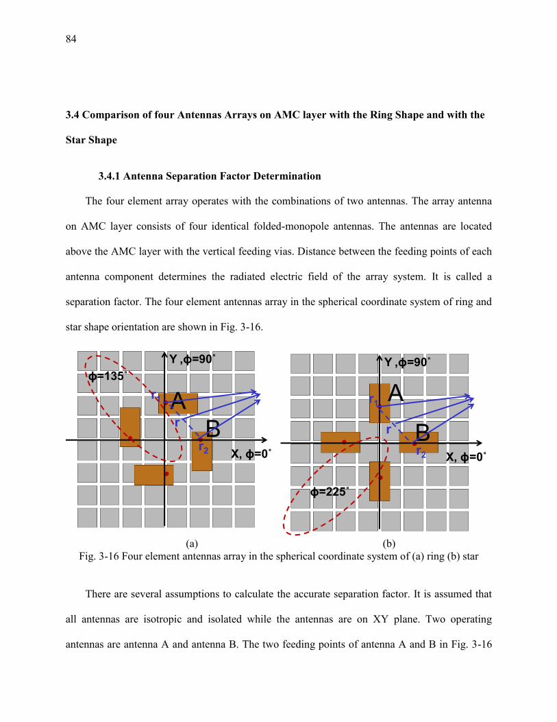
84
3.4 Comparison of four Antennas Arrays on AMC layer with the Ring Shape and with the
Star Shape
3.4.1 Antenna Separation Factor Determination
The four element array operates with the combinations of two antennas. The array antenna
on AMC layer consists of four identical folded-monopole antennas. The antennas are located
above the AMC layer with the vertical feeding vias. Distance between the feeding points of each
antenna component determines the radiated electric field of the array system. It is called a
separation factor. The four element antennas array in the spherical coordinate system of ring and
star shape orientation are shown in Fig. 3-16.
(a) (b)
Fig. 3-16 Four element antennas array in the spherical coordinate system of (a) ring (b) star
There are several assumptions to calculate the accurate separation factor. It is assumed that
all antennas are isotropic and isolated while the antennas are on XY plane. Two operating
antennas are antenna A and antenna B. The two feeding points of antenna A and B in Fig. 3-16
X, =0
Y =90
X, =0
Y =90
B
A
B
A
r2
r
r1
r2
r
r1

85
(a) and (b) are assumed to be equal to each other. The maximum directivity of two directional
antennas of the ring and star orientations are expected to be located at ϕ = 135 ˚ and ϕ = 225 ˚,
respectively, as shown in Fig. 3-16. The distance from the origin to the feeding points of antenna
A and B are equal to each other. The general electric field equation of two-array identical
antenna is shown below [66].
[
| |
| |
| |
| |]
The far-field approximations assuming the directional vectors are parallel to each other are
applied to the equation to simplify the problem as shown in Fig. 3-17.
(a) (b)
Fig. 3-17 Far-field approximation (a) ring (b) star
X, =0
Y =90
X, =0
Y =90
B
A
B
A
r2
r
r1
r2
r
r1

86
Fig. 3-18 Far field vector simplification
The directional vector is used for the phase of exponential function and the amplitude of the
E-field. The far-field approximations of phase and amplitude term are respectively,
| | [| |-
√ = [| |
√ (3.6)
| | [| |-
√ = [| |
√
| | | | | |
while | | = | + + |. The detail figure of the vector simplification is
shown in Fig. 3-18.
The approximations of (3.6), (3.7), and (3.8) are applied, (3.5) is re-written as
| |
| |
[ (
√ )
(
√ )
]
X, =0
Y =90 r1
r2
r
d/√2
d/√2
d(sinθcosΦ-sinθsinΦ)/2√2
d(sinθcosΦ-sinθsinΦ)/2√2

87
According to Euler’s Transfer, (3.10) and (3.11) are reduced to,
| |
| | (
√ )
when k=2π/λ.
The value of θ is fixed as 90˚ because the antennas are on XY plane. The equation (3.10) is
simplified as below.
| |
| | (
√ )
The array factor (AF), (
√ ) , determines the maximum gains and nulls
of the array antenna. Because the AF calculation is based on the assumption that the antennas are
isotropic, the locations maximum gain from the calculation includes the maximum directivity of
the directive array antenna. The plot of AF with ϕ = 45˚, 135˚, 225˚, and 315˚ along to the
distance of antenna feeding points are shown in Fig. 3-19. The AF has maximum directivity and
nulls when ϕ = 45˚ and 225˚, and ϕ = 135˚ and 315˚, at distance is 2.5 mm, which is λ/2. The
results of maximum directivity include the star orientation, but the maximum directivity of ring
orientation is not included. In conclusion, with the separation factor of λ/2, star orientation shows
better performance than the ring orientation. It is verified with HFSS in next section. Another
approach is shown in the Appendix A.
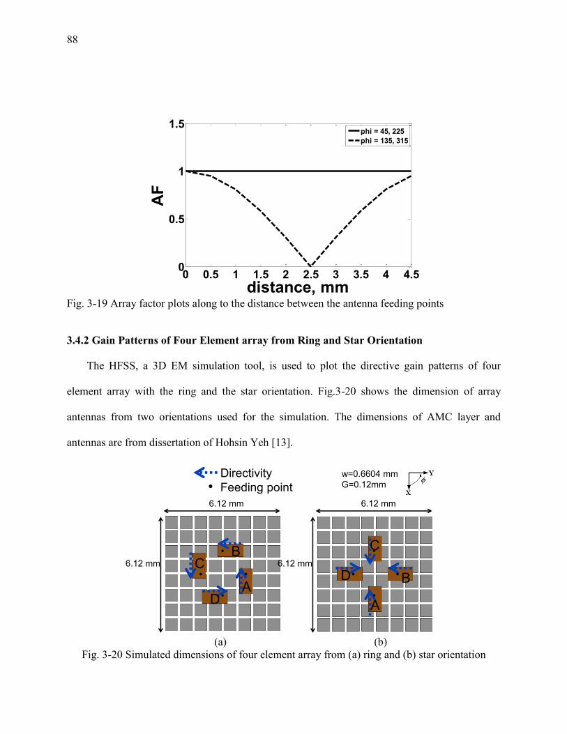
88
Fig. 3-19 Array factor plots along to the distance between the antenna feeding points
3.4.2 Gain Patterns of Four Element array from Ring and Star Orientation
The HFSS, a 3D EM simulation tool, is used to plot the directive gain patterns of four
element array with the ring and the star orientation. Fig.3-20 shows the dimension of array
antennas from two orientations used for the simulation. The dimensions of AMC layer and
antennas are from dissertation of Hohsin Yeh [13].
(a) (b)
Fig. 3-20 Simulated dimensions of four element array from (a) ring and (b) star orientation
0 0.5 1 1.5 2 2.5 3 3.5 4 4.50
0.5
1
1.5
distance, mm
AF
phi = 45, 225
phi = 135, 315
Directivity
Feeding point
6.12 mm
6.12 mm
6.12 mm
6.12 mm
w=0.6604 mm
G=0.12mm
AD
CB
C
A
D
B

89
The gain patterns with one antenna-on three antennas-off and with two antennas-on two
antennas-off are plotted. Antenna A is on for the single antenna excitation and antenna A and B
are on for the two antennas excitation. It is expected that the maximum gain of a single antenna
excitation is at ϕ = 180˚ and two antennas excitation is at ϕ = 225˚. The shape of the gain pattern
of the four element array with one antenna-on is expected to be different from the single antenna
because E-field interacts with other antennas and feeding vias. The interaction effect of the other
antennas is expected to be greater in the star orientation because a feeding via of an antenna is
placed at the direction of the maximum directivity. The location of each antenna in the ring
orientation at the center point is asymmetric, while the star orientation is symmetric. The
asymmetric structure of ring orientation possibly deteriorates the antenna radiation pattern in the
expected direction. The ring orientation has less obstacles then the star orientation structurally.
The positions of feeding points in the ring orientation are the same as the star orientation, with
λ/2 spacing factor.
Fig. 3-19 shows the gain patterns of the single and the two antennas from the ring and the
star orientations. The asymmetric structure of the ring orientation causes declined gain in the
expected direction, while the feeding via of antenna C generates a radiation null at ϕ=180˚ as
shown Fig. 3-21 (a). The gain shape of ring orientation is asymmetric while the star orientation
has a symmetric shape of gain. The symmetric structure of the antenna system results in a better
antenna gain as shown in Fig. 3-19 (b). The gain of two antennas from both the ring orientation
and star orientation have the maximum gain at ϕ=225˚. The gain value of star orientation is more
than 3 dB greater than the ring orientation.

90
Fig. 3-21Gain patterns of (a) single and (b) two antennas from the ring and star orientations
Table 3-3 Values and directions of four element array antenna gain
Orientation Excitation Maximum gain (dBi) aximum angle ( )
Ring One antenna 2.54 224
Two antennas 2.51 227
Star One antenna 4.19 220, 140
Two antennas 7.23 225
3.5 Four Elements Antennas Array Design
3.5.1 Initial Patch and Antenna Design
The patch dimension of the AMC layer is determined by HFSS simulation resulting in 0˚
reflection phase. The unit cell of the AMC layer with the rectangular waveguide simulator is
shown in Fig. 3-22. The values of g and h are fixed as 0.12 mm and 0.203 mm as described in
previous section. The HFSS simulation results of reflection phase with different W are shown in
Fig. 3-23. The value of W is determined with 56 mm.
˚
˚
˚ ˚
x
y -4
0
4
8 dB0
180
270 90 -4
0
4
8 dB
0
180
90270
Ring
Star ˚
˚
˚ ˚
x
y

91
Fig. 3-22 Unit structure and dimensions of periodic AMC layer
Fig. 3-23 Reflection phase with different W
0.203 mm
0.203 mm
0.203 mm
Patch
Ground
RO4003
Floquet port + M/S Boundary=Periodic Structure
50 55 60 65 70-180
-120
-60
0
60
120
180
Frequency, THz
Refl
ecti
on
Ph
ase,
deg
W=0.52mm
W=0.56mm
W=0.60mm

92
With the initial dimension of the AMC patch, the antenna dimension operating at 60 GHz is
determined. The on-chip antenna is a folded monopole antenna consisting of the vertical feed
and the printed board. The top view and profile of four element array with the dimension of the
AMC layer is shown in Fig. 3-24.
The antennas on the AMC layer are folded monopole antennas, including the feeding wire
and printed board. It is different from the planar inverted F antenna (PIFA) because the shorting
strip is removed. The dimension of folded monopole is determined by
when h1 and h2 are the height of RO4003 overlapped to the feeding vias, and λd is the resonant
wavelength with the dielectric superstrates [13]. The values of h1 and h2 are 0.203 mm as shown
in Fig. 3-23. The initial values of antl and antw are 0.4 mm and 0.75 mm, respectively. The gain
pattern and input impedance of the four antenna array are shown in Fig. 3-25 and 3-26,
respectively.
(a) (b)
Fig. 3-24 Four antenna array with the dimension of the AMC layer (a) top view (b) profile
0.203 mm
0.203 mm
Antenna
Patch
Ground
Inner conductor
Silicon
RO4003
0.56 mm
0.12 mmantw
antl
0.203 mm5.32 mm
5.32 mm
B
C
A
D

93
Fig. 3-25 Gain pattern of four array antenna with the initial values of W, antl, and antw
Fig. 3-26 Input impedance of four array antenna with the initial values of W, antl, and antw
0
5
10 dB0
180
270 90
˚
˚
˚ ˚
x
y
30 40 50 60 70 80 90
-200
-100
0
100
200
300
400
500
Frequency, GHz
Inp
ut
Imp
ed
an
ce, o
hm
Real
Imag

94
3.5.2 Antenna Tuning Process
The values of gain and input impedance are 5.47 dB and 16.40-j38.89 Ω, respectively. The
gain of four element array is better than the gain of a single antenna; however, the input
impedance is not matched well. The antenna is needed to be tuned to a larger dimension because
resonance region of the input impedance plot is higher than 60 GHz, as shown in Fig. 3-26. It is
because four antennas fabricated on the AMC layer create the interaction between the antennas
and patches, which causes the mismatch of input impedance and gain. The parametric study is
required to design an on-chip antenna with a reasonable directional gain pattern and well-
matched input impedance at 60 GHz.
All parameters, W, antl, and antw impact on both of gain and impedance matching but there
are majority effects of antenna parameters on each antenna characteristic. The dimension of
patch determines the characteristics of the AMC layer, which mainly relates to the directive gain
pattern at the resonant frequency. The antenna dimensions are the main factors to determine the
resonant frequency and input impedance. The tuning is conducted with the order of W, antl, and
antw with the assumption that other factors have less effect on the other antenna parameters to
simplify the process. The criteria to select the optimized value of W, antl, and antw are in the
order of strength of the impact on antenna characteristics. The first step of optimization is finding
the reasonable value of W creating an appropriate gain pattern. Three cores are located in one
side of a chip and the length is 20 mm. The width of one core, Wcore, is the maximum of 6 mm
that is the limit of the value of W. The value of Wcore has minimal limit to let the antennas be
located on the AMC layer to create an appropriate antenna operation. The minimum value of W
is 0.47 mm with antl = 0.75 mm. The value of W still requires enough margins for larger antl

95
because larger values of antl than 0.75 mm will be swept. The maximum value of W is 0.65 mm
due to the limit of Wcore, 6 mm. The gain and S11 with two antennas-on (antenna A and antenna B)
are measured with several values of W from 0.6 mm to 0.65 mm as shown in Table 3-4. The
value of gain is less than 5 dB with W is 0.6 mm and 0.63 mm. W is determined as 0.65 mm
because it has the maximum S11 among all W with the gain greater than 5 dB.
Table 3-4 Parametric study of antenna characteristics with W
WCore (mm) W (mm) S11 (dB) Input impedance (Ω) Gain 2Antennas @225° (dBi)
5.64 0.6 -3.23 16.59+j42.54 4.84
5.72 0.61 -3.2 15.75+j42.42 5.61
5.8 0.62 -2.8 13.66+j43.08 5.73
5.88 0.63 -2.96 15.47+j44.98 4.51
5.96 0.64 -3 15.5+j45.27 5.57
6.04 0.65 -3.37 17.67+j47.24 5.47
The antenna dimension is optimized with the selected W. The longer values than the initial
antl are swept because the resonant frequency needs to be shifted down. The value of antl is less
than 1.5 mm not to exceed the area of AMC layer. The antl is parameterized from 0.75 mm to
1.35 mm to give enough margins from the edge of AMC layer. The values of W and antw are
fixed as 0.65mm and 0.4 mm. The parameter study results are shown in Table 3-5.
The antenna impedance is well-matched to 50 Ω around the range of antl from 0.95 mm to
1.05 mm. The minimum S11 is -21.98 dB with antl = 1 mm. The gain of array antenna is
proportional to the value of antl that is greater or equal to 0.9 mm. The gain of array antenna with
1 mm of antl is 7.06 dB while the antenna with 1.35 mm antl has 8.38 dB. The value of antl is
determined as 1 mm because antl is tuned for the 50 Ω input impedance matching of antenna.
The optimized value of antw is 0.4 mm from the parametric study of antw as shown in Table 3-6.

96
Table 3-5 Parametric study of antenna characteristics with antl, when W = 0.65 mm
antl (mm) S11 (dB) Input impedance (Ω) Gain 2Antennas @225° (dBi)
0.75 -3.37 17.69+j47.24 5.47
0.8 -4.07 25.07+j54.43 5.14
0.85 -5.37 43.01+j60.15 4.88
0.9 -7.92 67.72+38.18 5.03
0.95 -12.67 58.5+j15.83 5.82
1 -21.98 56.88+j7.83 7.06
1.05 -18.82 44.96-j4.73 7.65
1.1 -12.67 33.1-j5.44 7.87
1.15 -9.76 26.02-j1.87 8.23
1.2 -8.33 22.5-j0.1 8.34
1.25 -7.32 19.89+j1.52 8.27
1.3 -6.48 17.89+j3.76 8.32
1.35 -6.03 16.74+j4.93 8.38
Table 3-6 Parametric study of antenna characteristics with antw when W = 0.65 mm and
antl = 1 mm
antw (mm) S11 (dB) Input impedance (Ω) Gain 2Antennas @225° (dBi)
0.4 -21.98 56.88+j7.83 7.06
0.5 -21.48 58.62+j9.09 7.3
0.6 -20.2 60.85+j11.16 7.57
0.7 -17.49 66.11+j14.82 7.56
0.8 -15.4 73.8+j16.56 7.61
0.9 -13.96 80.07+j20.49 7.53
1 -12.39 91.45+j22.93 7.4
The possible values of antw are 0.4 mm, 0.5 mm, and 0.6 mm by considering input
impedance and the gain at 225˚. The value of antw is determined with 0.4 mm due to the
impedance matching.
The value of antl was selected based on the input impedance matching, but the gain also can
be the criteria to determine antl from Table 3-8. The antenna gain is greater than 8 dB when antl
is between 1.15 mm and 1.35 mm. Antl is set with 1.2 mm which is the best input impedance

97
matched with the gain greater than 8 dB. It is assumed that antw is swept to match the input
impedance. The sweeping results show that 1 mm of antw shows the maximum gain at 225˚ and
matched input impedance.
Table 3-7 Parametric study of antenna characteristics with antw when W = 0.65 mm and
antl = 1.2 mm
antw (mm) S11 (dB) Input impedance (Ω) Gain 2Antennas @225° (dBi)
0.4 -8.33 22.5-j0.1 8.34
0.5 -9.96 26.29+j1.79 8.36
0.6 -11.78 30.12+j3.69 8.33
0.7 -14.11 34.82+j5.58 8.31
0.8 -17.29 40.28+j7.44 8.2
0.9 -21.85 47.36+j8.33 8.16
1 -29.52 56.23+j7.49 8.01
3.6 Results Analysis
The design tuning results are shown in Table 3-8. Both of cases show appropriate values of
combined gain and input impedance while case 2 shows better performance than case 1. The size
of fabricated antenna array in case 1 is smaller than case 2. Case 1 has better one-antenna-gain
than case 2. The gain of the final four array antenna and one antenna are shown in Fig. 3-27.
Both show great directivity in the expected direction with two antennas-on while one antenna
gain of case 2 is deteriorated. It is due to the greater interference between the antenna and
patches caused by the larger dimension of antenna.
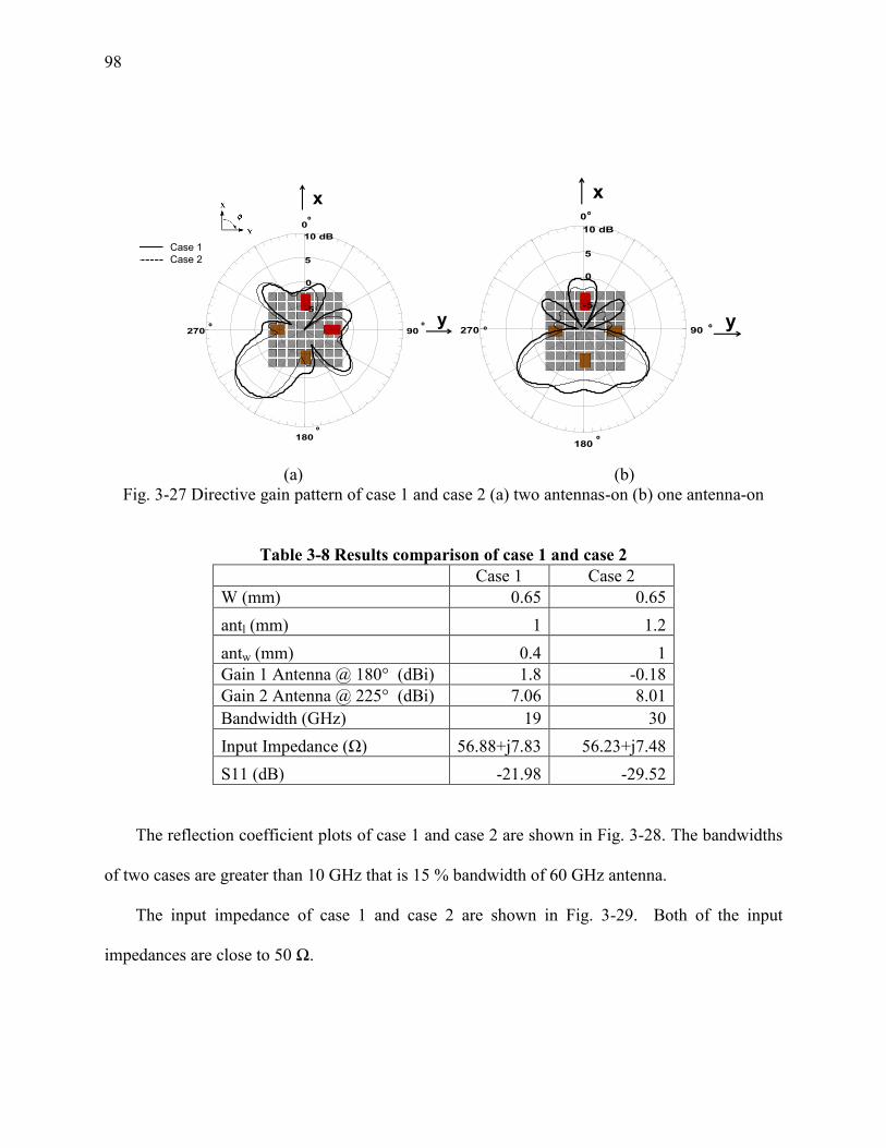
98
(a) (b)
Fig. 3-27 Directive gain pattern of case 1 and case 2 (a) two antennas-on (b) one antenna-on
Table 3-8 Results comparison of case 1 and case 2
Case 1 Case 2
W (mm) 0.65 0.65
antl (mm) 1 1.2
antw (mm) 0.4 1
Gain 1 Antenna @ 180° (dBi) 1.8 -0.18
Gain 2 Antenna @ 225° (dBi) 7.06 8.01
Bandwidth (GHz) 19 30
Input Impedance (Ω) 56.88+j7.83 56.23+j7.48
S11 (dB) -21.98 -29.52
The reflection coefficient plots of case 1 and case 2 are shown in Fig. 3-28. The bandwidths
of two cases are greater than 10 GHz that is 15 % bandwidth of 60 GHz antenna.
The input impedance of case 1 and case 2 are shown in Fig. 3-29. Both of the input
impedances are close to 50 Ω.
-5
0
5
10 dB
0
180
270 90
Case 1
Case 2
˚
˚
˚ ˚
x
y -5
0
5
10 dB
0
180
270 90
˚
˚
˚ ˚
x
y
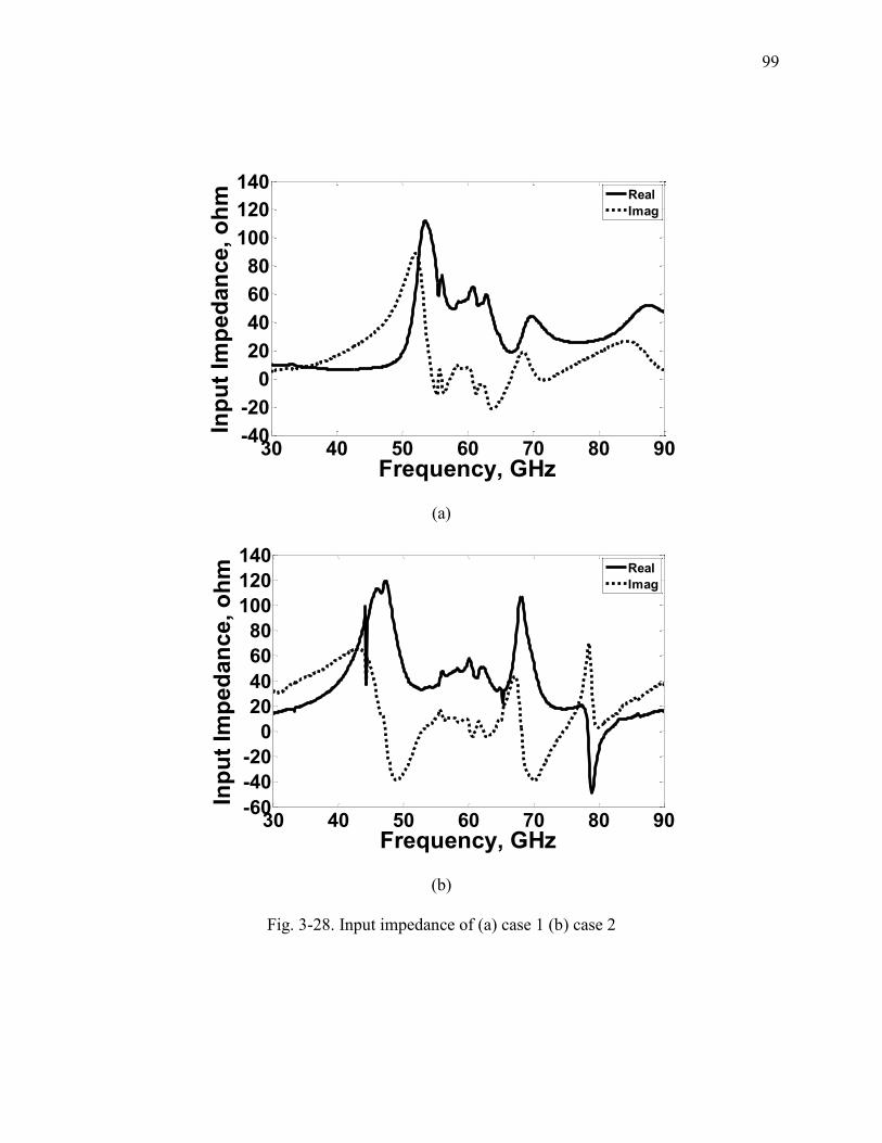
99
(a)
(b)
Fig. 3-28. Input impedance of (a) case 1 (b) case 2
30 40 50 60 70 80 90-40
-20
0
20
40
60
80
100
120
140
Frequency, GHz
Inp
ut
Imp
ed
an
ce, o
hm
Real
Imag
30 40 50 60 70 80 90-60
-40
-20
0
20
40
60
80
100
120
140
Frequency, GHz
Inp
ut
Imp
ed
an
ce, o
hm
Real
Imag

100
Fig. 3-29 Reflection coefficients of case 1 and case 2
The wireless link budget denotes the efficiency of case 1 and case 2 as shown in Fig. 3-30.
The values of PRE and Budgets of case 1 and case 2 are improved compare to Fig. 3-12. The
power recovered of one antenna-on of the case 1 is lower than case 2 because of the lower gain.
The case 2 with two antennas-on shows better PRE than case 1. The Budget considering the
bandwidth of S11 shows case 2 has more efficient antenna than case 1 due to the wider bandwidth.
30 40 50 60 70 80 90-50
-40
-30
-20
-10
0
Frequency, GHz
Refl
ecti
on
Co
eff
icie
nt,
dB
case 1
case 2
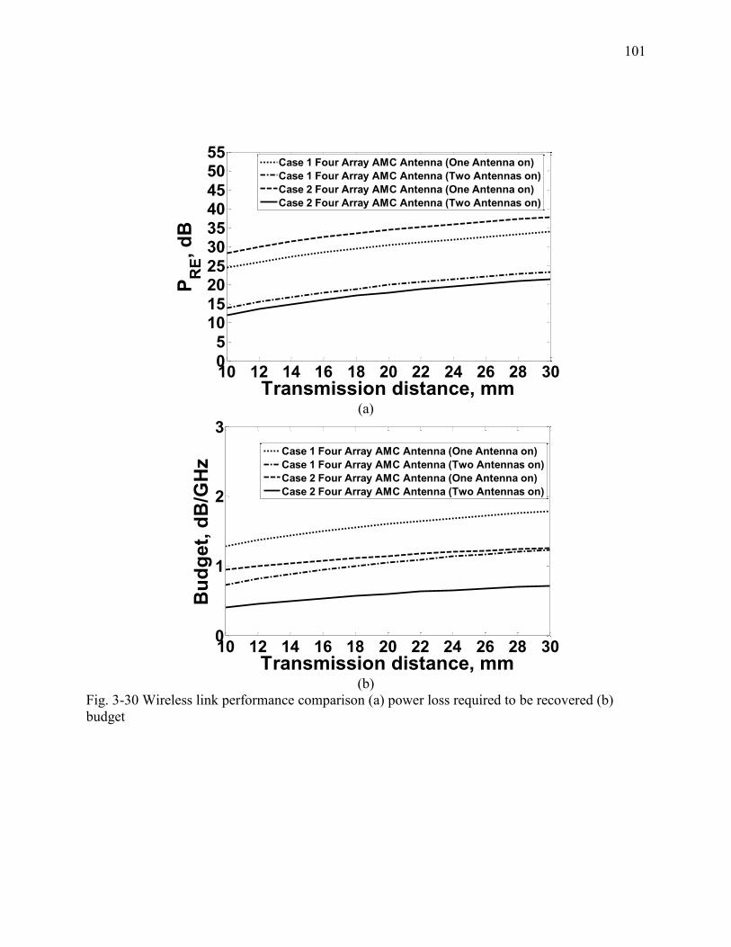
101
(a)
(b)
Fig. 3-30 Wireless link performance comparison (a) power loss required to be recovered (b)
budget
10 12 14 16 18 20 22 24 26 28 300
5
1015
2025
3035
4045
5055
Transmission distance, mm
PR
E, d
B
Case 1 Four Array AMC Antenna (One Antenna on)
Case 1 Four Array AMC Antenna (Two Antennas on)
Case 2 Four Array AMC Antenna (One Antenna on)
Case 2 Four Array AMC Antenna (Two Antennas on)
10 12 14 16 18 20 22 24 26 28 300
1
2
3
Transmission distance, mm
Bu
dg
et,
dB
/GH
z
Case 1 Four Array AMC Antenna (One Antenna on)
Case 1 Four Array AMC Antenna (Two Antennas on)
Case 2 Four Array AMC Antenna (One Antenna on)
Case 2 Four Array AMC Antenna (Two Antennas on)

102
CHAPTER 4 GENERALIZATION OF VHF ZIGZAG ANTENNA
4.1 Introduction
There has been increased interest in monitoring the potential effects of environmental
pollutants and global warming on the Earth. One way to quantify the potential effects of these
factors are to measure the rate of habitat decline of animal species most impacted. The data
analysis of the animal behaviors can help monitor the current surroundings of habitats where the
animals live. A wildlife tracking system is the starting point of the animal behavior research.
A wildlife tracking system should use antennas that do not interfere with the natural
behavior of the animal. An appropriate candidate antenna should be low-profile, have omni-
directional beam coverage in the horizontal direction, and adequate bandwidth performance [72].
The radio system can be relatively low data rate compared to commercial handheld wireless
systems used for human point-to-point communications. The wildlife tracking systems work in
remote areas and cannot rely on an existing cellular infrastructure.
One possible wildlife tracking system is a commercial wireless system used for training dogs
for recreational hunting. There is a substantial commercial market for wireless systems to keep
track of hunting dogs in a forested region, Fig. 4-1 [73]. The communication system uses one
device with a monopole antenna worn on the dog collar. Another handheld device is used by the
owner. The collar worn system consists of two antennas and corresponding radio systems; one is
a GPS (receive only) system that obtains the correct location of the dog, and the other is a
terrestrial system that transmits the location information to the handset of the owners. One link
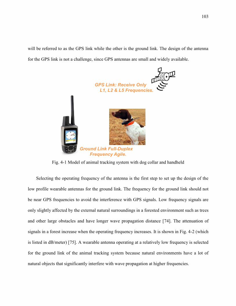
103
will be referred to as the GPS link while the other is the ground link. The design of the antenna
for the GPS link is not a challenge, since GPS antennas are small and widely available.
Fig. 4-1 Model of animal tracking system with dog collar and handheld
Selecting the operating frequency of the antenna is the first step to set up the design of the
low profile wearable antennas for the ground link. The frequency for the ground link should not
be near GPS frequencies to avoid the interference with GPS signals. Low frequency signals are
only slightly affected by the external natural surroundings in a forested environment such as trees
and other large obstacles and have longer wave propagation distance [74]. The attenuation of
signals in a forest increase when the operating frequency increases. It is shown in Fig. 4-2 (which
is listed in dB/meter) [75]. A wearable antenna operating at a relatively low frequency is selected
for the ground link of the animal tracking system because natural environments have a lot of
natural objects that significantly interfere with wave propagation at higher frequencies.
GPS Link: Receive Only
L1, L2 & L5 Frequencies.
Ground Link Full-Duplex
Frequency Agile.

104
Fig. 4-2 Wave attenuation in forested regions as a function of frequency
Multi-Use Radio Service (MURS) band is used for the operating frequency of the tracking
system. In the USA, MURS requires no licensing and frequency coordination; hence it is a
simple and cost-effective solution. The MURS consists of five VHF frequencies as depicted in
Table 4-1 [76].
Table 4-1 MURS frequency designation
MURS Frequencies (MHz) Authorized Bandwidth (kHz)
151.82 11.25
151.88 11.25
151.94 11.25
154.57 20
154.6 20
100 200 300 40010
-2
10-1
100
Frequency, MHz
Att
en
ua
tio
n,
dB
/m

105
One potential solution for VHF wearable animal collar antennas is the zigzag antenna. The
characteristics of the zigzag antenna are similar to the ones of a monopole antenna because the
zigzag antenna is designed by meandering the monopole antenna. Zigzag antennas are wire
antennas that have successive bends, with practical operating frequencies from 3MHz to 3GHz
[77]. The overall wire length is similar to monopole wire length, but the antenna height is more
compact [78]. An example zigzag antenna is shown in Fig. 4-3 [79].
Fig. 4-3 Upright zigzag antenna [79]

106
The wearable zigzag antenna is different from the upright zigzag antenna in that it is curved
and integrated into collars. The collar integrated zigzag antenna is easy to wear, safe from impact
with objects, and stably fixed on the body of animals. The proposed zigzag antenna placed
around a phantom dielectric cylinder that represents the animal body is shown in Fig. 4-4. The
result is a shortened monopole antenna that will include a ground plane and shorting strip to
create suitable impedance matching. The final antenna is curved and flexible in order to fit
within the confines of a collar, and works in the presence of the animal’s body. The meandering
antenna to the zigzag shape and placing the antenna structure nearby the body phantom of the
animal are modeling challenges. The design procedure of wearable zigzag antenna mounted on
animal collars to be used for tracking their movements is introduced in [3].
Fig. 4-4 Collar integrated zigzag antenna
103.83 mm

107
The zigzag antenna in this work consists of a small ground plane, upright part length of
antenna, the number of pieces of the zigzag, and the overall radius of curvature on the animal
neck. A small black circuit box that houses the transceiver on the collar is treated as a small
ground plane. The upright part length of antenna, angle and number of zigzag are factors to be
determined for optimized zigzag antenna design.
4.2 Zigzag Antenna Design Process
The wearable VHF zigzag tracking antenna possibly has broad applications, house cats,
golden tamarins, people, or polar bears. The design process of the zigzag antenna needs to be
generalized to be applied to other applications. Small ground effect, meandering the antenna to
the zigzag shape, and T-matching methods are the common design area of all applications with
different dimension of body phantoms. In this Section, the common design steps of zigzag
antenna are generally analyzed.
4.2.1 Small Ground Effects
The infinite ground plane impacts the radiated waves from the monopole antenna by image
effects [11]. The typical directivity of the monopole antenna with an infinite ground plane is
about 5.23 dB. To quantify the effect of a small ground plane, a sample structure is modeled by
computational simulation, high frequency structural simulation (HFSS) from Ansys Co. [49].
The dimensions of the ground plane, as shown in Fig. 4-1, are 75 x 45 mm2 is considered. The
monopole antenna is 473 mm and placed on the small ground plane as shown in Fig. 4-5. The
plots of return loss are shown in Fig. 4-6, and simulation results are in Table 4-2.

108
Fig. 4-5 Monopole antenna on the small ground plane
Fig. 4-6 Return loss of monopole antenna on the small ground plane and infinite ground
plane
x y
z
473 mm
50 100 150 200 250 300
-15
-10
-5
0
Frequency, MHz
Inp
ut
Imp
ed
an
ce
Monopole with small GND
Monopole with large GND
Retu
rn L
oss, d
B

109
Table 4-2 Antenna characteristics of the monopole antenna on an infinite and a small
ground plane
Infinite ground Small ground
Resonant frequency (MHz) 153 153
Return loss (dB) -14.71 -15.46
Input impedance (Ω) 35.25+j5.36 36.43+j5.38
Directivity (dB) 5.23 2.95
The return loss is dB scale of the reflection coefficient. The equation of reflection coefficient
is
where Zantenna and Zport are the impedance of antenna and input port, and V+ and V
- are the
voltage of input wave and reflected wave. If the input impedance of antenna and input port are
well matched, there is no reflected wave, so reflection coefficient is close to 0, which means very
small return loss.
The radiation patterns of monopole antenna on aninfinite ground plane and small ground
plane are shown in Fig. 4-7.
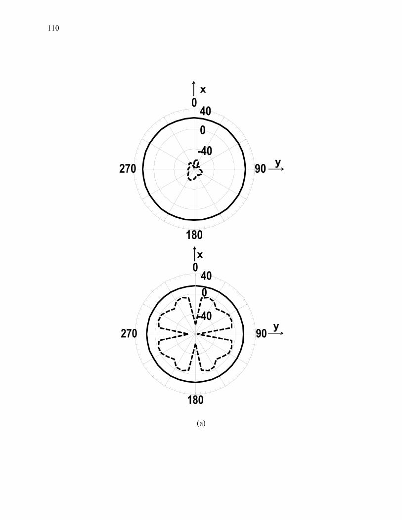
110
(a)
-40
0
400
180
270 90
x
y
-40
0
400
180
270 90
x
y

111
(b)
-40
0
400
180
270 90
Z
y
-40
0
400
180
270 90
Z
y

112
(c)
4-7 E-field pattern of the monopole antenna on the infinite ground plane (top) and small ground
plane (bottom) (a) XY plane (b) YZ plane (c) ZX plane
-40
0
400
180
270 90
Z
X
-40
0
400
180
270 90
Z
X
100 110 120 130 140 150 160 170 180 190 200-50
0
50
100
Frequency, MHz
Inp
ut
Imp
ed
an
ce
Real 141 MHz
Imag 141 MHz
Real 153 MHz
Imag 153 MHz
Eθ
100 110 120 130 140 150 160 170 180 190 200-50
0
50
100
Frequency, MHz
Inp
ut
Imp
ed
an
ce
Real 141 MHz
Imag 141 MHz
Real 153 MHz
Imag 153 MHz
Eϕ

113
4.2.2 Meandering the Antenna to the Zigzag Shape
Meandering is the key point of the zigzag antenna design. The meandering antenna design
lists are,
The length of the straight section of the antenna.
The angle of the zigzag piece.
The number of the zigzag and the dimensions of the zigzag.
The number and the dimensions of zigzag can be determined when the specific application of
the zigzag antenna is known. Therefore, the last factor is discussed in the Section 4.3. In this
section, the general design factors are described.
Determining the starting point of the meandering zigzag is the initial procedure of the upright
zigzag antenna design. Some length of straight wire is required before the zigzag sections begin
because meandering the wire antenna around the input port affects the resonant frequency by
creating capacitance. The components of the upright zigzag antenna are shown in Fig. 4-8. The
length of the straight section is L1, the width and length of single bent section are W2 and L2,
respectively, and N is the number of bends.

114
Fig. 4-8 Geometry of an upright zigzag antenna
All components are related to each other as shown below because the total length of the
antenna is constant. The total length of the antenna is λ/4, where λ is the wavelength at 153 Hz.
√
(a) (b) (c) (d)
Fig. 4-9. Four antennas with different L1 and N=1 (a) L1 =0 (b) L1 =L/10=47.3 mm (c) L1 =L/5=94.6 mm (d) L1 =L/2=236.52 mm
L1
L2
W2
L2 : Length of Antenna2
W2 : Width of Antenna2
L1 : Length of Antenna1
N : # of Zigzag
α : Angle of Zigzagα

115
Table 4-3 Comparison of simulation results from four zigzag antennas with
different L1
L1 (mm) 0 47.3 94.6 236.52
Input impedance (Ω) 7.74-j61.72 10.55-j50.75 13.66-j45.61 23.51-j29.88
Electric field at Top (V/m) 3.74E+04 2.71E+04 2.00E+04 8.79E+03
Electric field at Feed (V/m) 1.74E+04 1.36E+04 1.23E+04 1.20E+04
A short L1 can give more pieces of zigzags, yet the antenna has a large value of capacitive
impedance. The suitable value of L1 is determined by a parametric study using HFSS. Zigzag
antennas with different L1 are shown in Fig. 4-9, and the input impedance values and the
electrical field values measured at the top and feed point of zigzag antennas with different L1 are
shown in Table 4-3 The design with zero L1 shows a large capacitive input impedance. The
values of electric field strength at top and feed point of antennas decrease as L1 increased. The
value of L/10 is used as the L1.
Folding the monopole antenna wire into a zigzag antenna causes coupling capacitance
between the adjacent pieces of the antenna. Introduction of additional capacitance in the zigzag
antenna creates a negative reactance at the resonant frequency of the straight monopole antenna.
The capacitance between the antenna pieces is determined by electric field distribution of
antenna as the equation below [26]. The coupling capacitance creates a negative reactance
because there are other induced electromagnetic fields.
| | ∫

116
Table 4-4 Antenna characteristics with different angles of zigzag
α (˚) 30 60 90
Input impedance (Ω) 4.33-j85.27 10.55-j50.75 19.03-j26.18
Height of antenna (mm) 157.49 260.17 348.34
Electric field at Top (V/m) 3.08E+04 2.71E+04 1.22E+04
Electric field at Feed (V/m) 2.09E+04 1.36E+04 1.04E+04
The angle of the zigzag is another key factor to determine. Small angles reduce the total
height of the antenna, but the capacitance between the wires increases. A mid-range value of
angle is desired to strike a balance between the coupling capacitance and total height of antenna.
A parametric study using HFSS shows the change of antenna characteristics and the height of the
antenna, while the angle changes. The change of the antenna height and the antenna
characteristics are shown in Table. 4-4. The values of E field on the top and feed point of antenna
are reduced as the angle increase because the coupling capacitance is reduced. The input
impedance mismatch caused by relatively small values of L1 and the angle is compensated for
using input impedance matching methods discussed in the next section.
4.2.3 Antenna Input Impedance Matching Methods
Meandering the monopole antenna into a zigzag antenna and integrating it on the body of
animal creates the input impedance mismatch compared to a 50 Ω feed line. Simple, low cost,
and rugged matching methods are desired for the utilization in the cold and wet natural
environments. In general, the goal is to match the input impedance at the antenna port to 50 Ω
over a relatively narrow frequency band around 153 MHz. Two input impedance matching
methods, length tuning and T-matching, are introduced in this section.

117
Table 4-5 Antenna characteristics of 473.04 mm and 513.3 mm monopole antennas
Height (mm) 473.04 513.3
Resonant frequency (MHz) 153 141
Input impedance at 153 Hz (Ω) 35.25+j5.36 44.27+j52.02
Input impedance at resonant frequency (Ω) 32.97-j0.24 41.93+j50.38
Length tuning is performed by simply adding or removing zigzag pieces on the zigzag
antenna. The input impedance of a long monopole wire antenna has more resistance and
inductance compared to a shorter monopole antenna at the same frequency. A longer antenna
generates additional magnetic field which increases inductance, as shown in Fig. 4-10 and Table
4-5. Similarly adding zigzag pieces makes the input impedance inductive with more resistance,
while removing zigzag pieces makes the input impedance to capacitive with low resistance, at
the same frequency. Fig. 4-11 shows two zigzag antennas; one is created from a shorter
monopole antenna and the other from a longer monopole antenna. The length tuning approach
(adding more zigzag pieces) shifts the resonant frequency back to the desired frequency, but the
input impedance is not matched to the 50 Ω feed line. The T-matching method used to match the
input impedance of the PIFA to 50 Ω will be applied to the zigzag antenna [13] [14].
Fig. 4-10 Impact of adding zigzag sections
Added resistance and inductance

118
Fig. 4-11. Length tuning method
T-matching is a matching method created by implanting a T-shaped shorting pin wire
between the ground plane and the antenna [66]. It also acts as a balun between the antenna and
outer conductor of the coaxial feed terminated with the small ground plane. The principal of the
T-matching method is shown in Fig. 4-12 [3]. The current path flows from the input port to the
end of antenna without any current leakage in Fig. 4-12 (a). An antenna model with a shorting
pin is shown in Fig. 4-12 (b). The current path flowing into the antenna is split to the antenna and
shorting pin as shown in Fig. 4-12 (b). The current at the feed point of the antenna with a
shorting pin is greater than the current at the feed point of the antenna without a shorting pin
because of an additional current channeled into the shorting pin, as shown in Fig. 4-12 (b). The
added shorting pin in parallel to the antenna creates different values of input voltage. The input
impedance of the antenna with a shorting pin is defined by different input voltage and current,
Vin’ and Iin’, which are determined by the total length of the shorting pin. This allows additional
control of the reactance at the feed point.
153 MHz
473 mm
199 MHz
10 pieces
187 MHz
111 pieces
141 MHz
513 mm

119
(a) (b)
Fig. 4-12. Depiction of current flow on (a) antenna without shorting pin and (b) antenna with a
shorting pin
A parametric study was conducted using HFSS to optimize the size of the shorting pin. The
current distributions in 473 mm long monopole antenna with an infinite ground plane and the
shorting pin are shown in Fig. 4-13. The height is set to 15 mm, and the lengths of the shorting
pin are 5 mm, 40 mm, and 140 mm. The largest input current is leaked into the shorting pin
when the shorting pin length is 5 mm. The antenna with a 5 mm long shorting pin is almost
shorted out because the relatively short copper piece has very small impedance. The current
leakage into the shorting pin is smaller and the amount of current that flows into the antenna is
increased with long shorting pins. It is because a short copper wire has almost zero resistance,
while a long copper wire has some value of resistance. Table 4-6 shows input impedance values
of the antenna with a 15 mm height and different lengths of shorting pins. The input impedance
is close to 50 Ω for the longer shorting pin cases.
Zin=Vin/Iin=36+j5Ω
Zo=50Ω
Iin
Zo=50Ω
Zin’=Vin’/Iin’=50Ω
Isp
Iin’ =Iin’’ + Isp
Vin Vin’
Iin’’
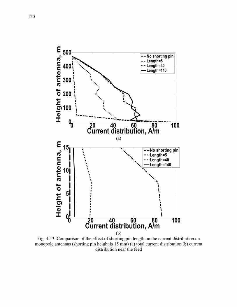
120
(a)
(b)
Fig. 4-13. Comparison of the effect of shorting pin length on the current distribution on
monopole antennas (shorting pin height is 15 mm) (a) total current distribution (b) current
distribution near the feed
0 20 40 60 80 1000
100
200
300
400
500
Current distribution, A/m
Heig
ht
of
an
ten
na, m
m
No shorting pinLength=5Length=40Length=140
0 20 40 60 80 1000
5
10
15
Current distribution, A/m
He
igh
t o
f an
ten
na,
mm
No shorting pinLength=5Length=40Length=140
0 20 40 60 80 1000
5
10
15
Current distribution, A/m
Heig
ht
of
an
ten
na, m
m
No shorting pinLength=5Length=40Length=140

121
Table 4-6 Input impedance of antenna as a function of 15 mm height and different length
of shorting pin
Length (mm) Input impedance at 153 Hz (Ω)
0 35.25+j5.36
5 1.82+j14.76
40 25.27+j32.24
140 42.40+j9.69
The input impedance comparison of the 473 mm line monopole over an infinite ground
plane without shorting pin, and with 5 mm, 40 mm, and 140 mm shorting pins are shown in Fig.
4-14. The input impedance of antenna with shorting pin shows the peak of anti-resonance before
the resonance frequency. The reactance is highly inductive around the anti-resonance region, and
becoming to zero around the resonance frequency.
The resistance has similar a trend as the reactance at lower frequency, and is becoming
around 50 Ω at the resonant frequency. The input impedance of antenna with 5 mm shorting pin
has a weak anti-resonance region with small resistance and reactance. There is no anti-resonance
before the resonance frequency in the input impedance plot of antenna without shorting pin. In
conclusion, the shorting pin matches the input impedance of antennas to 50 Ω with well-
distributed incident current by generating a strong anti-resonance region. The ideal dimension of
the shorting pin is longer than 100 mm. However, the size of the ground plane size does not
allow the long shorting pin. If the length of the shorting pin is relatively short, the resonant
frequency is formed at a lower frequency because the shorting pin creates inductive input
reactance.
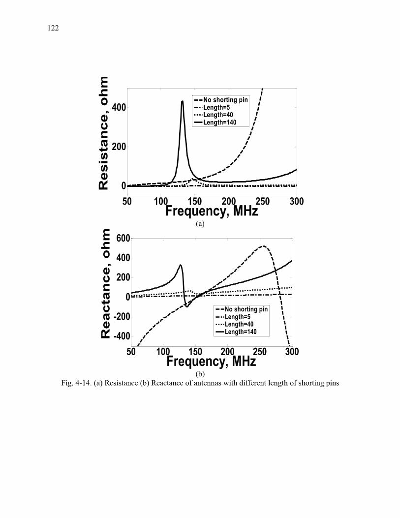
122
(a)
(b)
Fig. 4-14. (a) Resistance (b) Reactance of antennas with different length of shorting pins
50 100 150 200 250 300
0
200
400
Frequency, MHz
Resis
tan
ce,
oh
m
No shorting pinLength=5Length=40Length=140
50 100 150 200 250 300
-400
-200
0
200
400
600
Frequency, MHz
Re
ac
tan
ce,
oh
m
No shorting pinLength=5Length=40Length=140

123
4.3 Polar Bear Tracking Antenna
The polar bear is a valuable animal to study because it is an indicator of environment in the
Arctic. They spend most of their lives in remote areas, and live on the ice and even at sea on
large ice flows. Polar bears have black skin under white hair to absorb as much heat as possible
[80]. The bears have a layer of fat to be able to swim in the icy Arctic Ocean without freezing.
The polar bears are on the Red List of Threatened Species by the International Union for
Conservation of Nature and Natural Resources (IUCN), regarded as species on the brink of
extinction [81][82]. Green house effects have raised the Earth’s average temperature and
decreased amount of ice in the Arctic, and resulted in a decrease in the polar bear population.
The wearable zigzag antenna design for the polar bear is a starting point to research the behavior
of polar bear to track the situation of the North Pole.
4.3.1 Upright Zigzag Antenna for Polar Bear
The first step of the wearable zigzag antenna design is an upright zigzag antenna design
suitable for the polar bears. Determining the number of zigzag section (N) is the next step of the
upright zigzag antenna design. Changing N will affect the value of W2 (shown in Fig. 4-8) for
given a fixed length of L. Equation (4.3) shows the relation between N and W2.
(
)
In this case, L=473 mm and L1=47.3 mm. An angle set at 60˚ results in an antenna with a
practical height. The parametric study of HFSS shows how the return loss of the zigzag antenna
changes when N increases. The antennas with different N are shown in Fig. 4-15. W2 and the

124
input impedance dependence on N are shown in Table 4-7. The reactance of input impedance at
153 MHz. The reactance value can be tuned by adding several pieces of zigzag. The magnitude
of the reactance increases as N increases, but the real part of the input impedance has a small
change. The zigzag antenna will be integrated on the collar, so W2 should be smaller than the
width of the collar, 25 mm. The value of N is selected to be 10 by considering the proper value
of W2 and input reactance. Final impedance matching is performed as the final step in the design.
The dimension of upright zigzag antenna with N=10 is shown in Fig. 4-16.
(a) (b) (c) (d)
Fig. 4-15 Four antennas with different N (α=60˚, and total length=473 mm)
(a) N=0 (b) N =5 (c) N=10 (d) N=15
Table 4-7 Input impedance and W2 with different N (α=60˚, and total length=473 mm)
N 0 5 10 15
W2 (mm) 0 36.3 18.43 12.1
Input impedance (Ω) 36.43+j5.37 9.59-j118.82 8.89-j155.13 8.65-j174.46
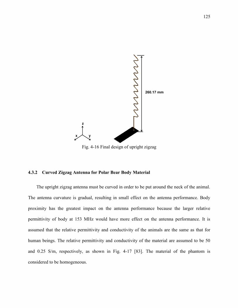
125
Fig. 4-16 Final design of upright zigzag
4.3.2 Curved Zigzag Antenna for Polar Bear Body Material
The upright zigzag antenna must be curved in order to be put around the neck of the animal.
The antenna curvature is gradual, resulting in small effect on the antenna performance. Body
proximity has the greatest impact on the antenna performance because the larger relative
permittivity of body at 153 MHz would have more effect on the antenna performance. It is
assumed that the relative permittivity and conductivity of the animals are the same as that for
human beings. The relative permittivity and conductivity of the material are assumed to be 50
and 0.25 S/m, respectively, as shown in Fig. 4-17 [83]. The material of the phantom is
considered to be homogeneous.
x y
z
260.17 mm
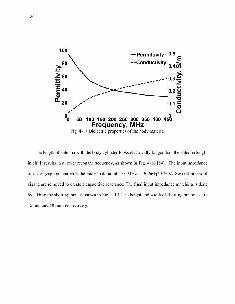
126
Fig. 4-17 Dielectric properties of the body material
The length of antenna with the body cylinder looks electrically longer than the antenna length
in air. It results in a lower resonant frequency, as shown in Fig. 4-18 [84]. The input impedance
of the zigzag antenna with the body material at 153 Hz is 30.66+j20.76 Ω. Several pieces of
zigzag are removed to create a capacitive reactance. The final input impedance matching is done
by adding the shorting pin, as shown in Fig. 4-19. The height and width of shorting pin are set to
15 mm and 50 mm, respectively.
0 50 100 150 200 250 300 350 400 4500
20
40
60
80
100
Pe
rmit
tiv
ity
0 50 100 150 200 250 300 350 400 4500
0.1
0.2
0.3
0.4
0.5
Frequency, MHz
Co
nd
uc
tivit
y,
S/mConductivity
Permittivity

127
Fig. 4-18 Input impedance change by meandering
Fig. 4-19 Final collar integrated zigzag antenna configuration
103.83 mm
x
y
z
25 mm
103.83 mm
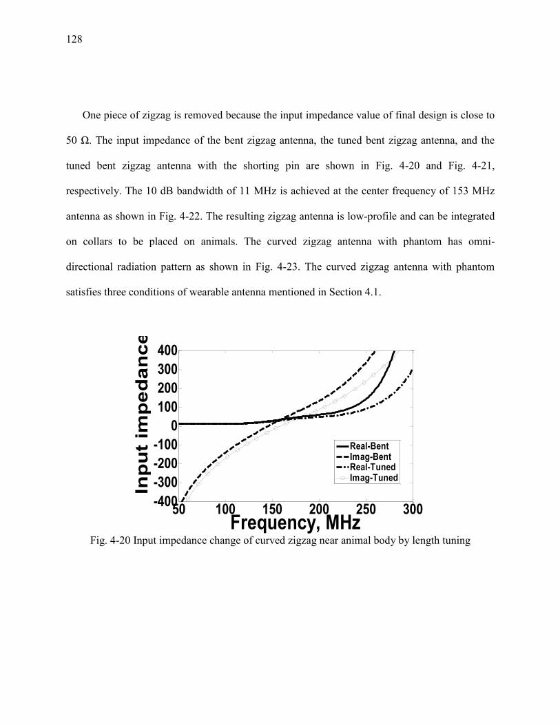
128
One piece of zigzag is removed because the input impedance value of final design is close to
50 Ω. The input impedance of the bent zigzag antenna, the tuned bent zigzag antenna, and the
tuned bent zigzag antenna with the shorting pin are shown in Fig. 4-20 and Fig. 4-21,
respectively. The 10 dB bandwidth of 11 MHz is achieved at the center frequency of 153 MHz
antenna as shown in Fig. 4-22. The resulting zigzag antenna is low-profile and can be integrated
on collars to be placed on animals. The curved zigzag antenna with phantom has omni-
directional radiation pattern as shown in Fig. 4-23. The curved zigzag antenna with phantom
satisfies three conditions of wearable antenna mentioned in Section 4.1.
Fig. 4-20 Input impedance change of curved zigzag near animal body by length tuning
50 100 150 200 250 300-400
-300
-200
-100
0
100
200
300
400
Frequency, MHz
Inp
ut
imp
ed
an
ce
Real-BentImag-BentReal-TunedImag-Tuned

129
Fig. 4-21 Input impedance change of curved zigzag near animal body by length tuning and
shorting pin
Fig. 4-22 10 dB bandwidth of the zigzag antenna
50 100 150 200 250 300-400
-300
-200
-100
0
100
200
300
400
Frequency, MHz
Inp
ut
imp
ed
an
ce
Real-TuneImag-TuneReal-SPImag-SP
50 100 150 200 250 300-15
-10
-5
0
Frequency, MHz
Re
flecti
on
Co
eff
icie
nt,
dB

130
(a)
(b)
-40
0
40 dB0
180
270 90
x
y
-40
0
40 dB0
180
270 90
z
y
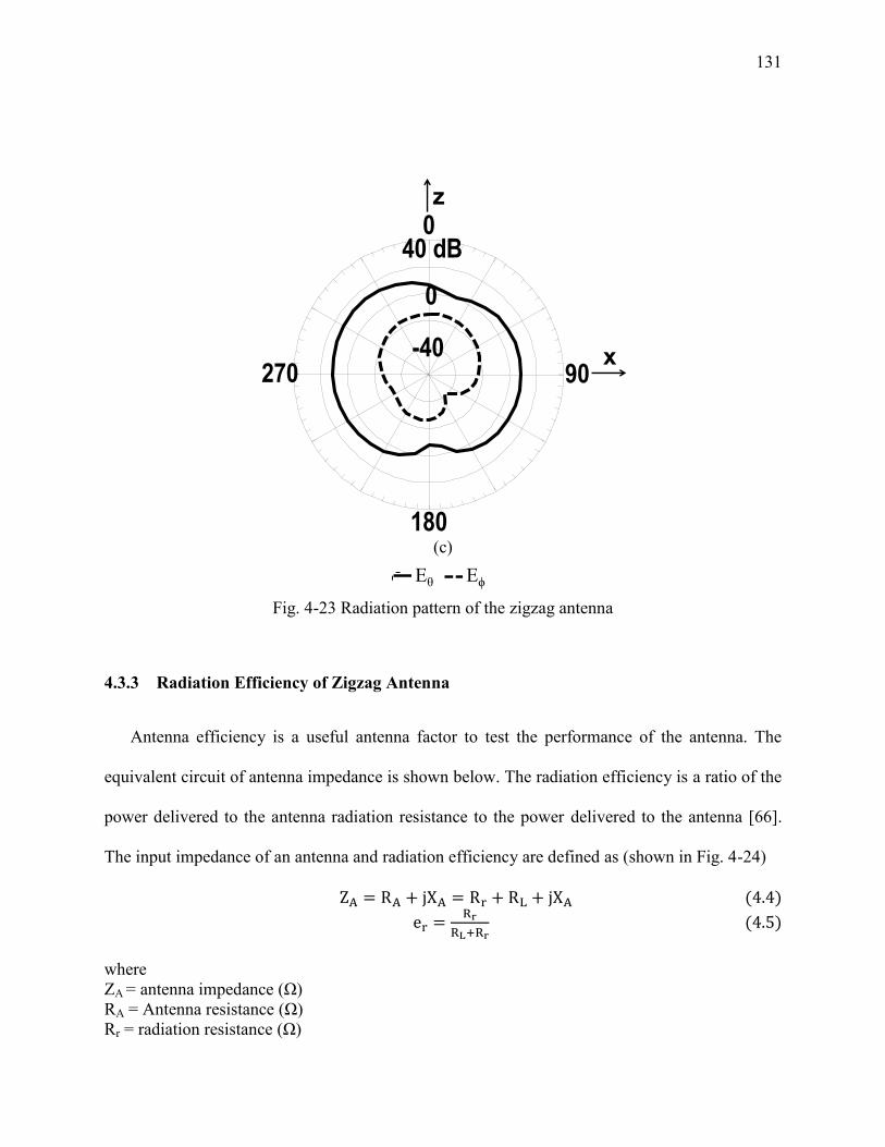
131
(c)
Fig. 4-23 Radiation pattern of the zigzag antenna
4.3.3 Radiation Efficiency of Zigzag Antenna
Antenna efficiency is a useful antenna factor to test the performance of the antenna. The
equivalent circuit of antenna impedance is shown below. The radiation efficiency is a ratio of the
power delivered to the antenna radiation resistance to the power delivered to the antenna [66].
The input impedance of an antenna and radiation efficiency are defined as (shown in Fig. 4-24)
where
ZA = antenna impedance (Ω)
RA = Antenna resistance (Ω)
Rr = radiation resistance (Ω)
-40
0
40 dB0
180
270 90
z
x
100 110 120 130 140 150 160 170 180 190 200-50
0
50
100
Frequency, MHz
Inp
ut
Imp
ed
an
ce
Real 141 MHz
Imag 141 MHz
Real 153 MHz
Imag 153 MHz
Eθ
100 110 120 130 140 150 160 170 180 190 200-50
0
50
100
Frequency, MHz
Inp
ut
Imp
ed
an
ce
Real 141 MHz
Imag 141 MHz
Real 153 MHz
Imag 153 MHz
Eϕ

132
RL = antenna loss resistance (Ω)
XA = antenna reactance (Ω)
er = radiation efficiency (dimensionless)
Fig. 4-24 Equivalent circuit of antenna impedance
Wheeler suggested a method to measure the antenna efficiency in 1959 [85]. The antenna is
covered by a metal cap with high conductivity. The dimension of the cap is greater or equal to
λ/2π to all directions from the antenna. The cap cancels out far-field radiation by reflecting all
electric field radiation from the antenna. The radiation impedance of the antenna with Wheeler
cap has zero value of Rr and only RL is measured. Therefore, the radiation efficiency of an
antenna is
where
RNoWheelerCap = resistance of antenna without Wheeler cap (Ω)
RWheelerCap = resistance of antenna with Wheeler cap (Ω)
RL
XA
Rr
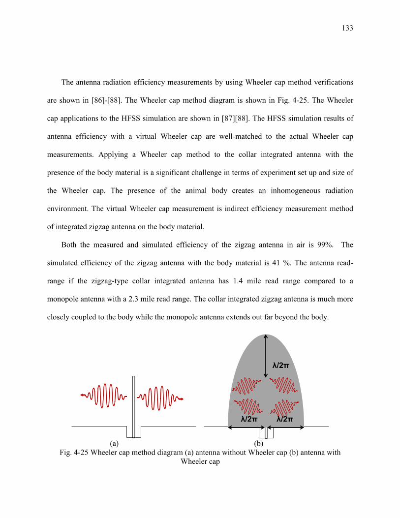
133
The antenna radiation efficiency measurements by using Wheeler cap method verifications
are shown in [86]-[88]. The Wheeler cap method diagram is shown in Fig. 4-25. The Wheeler
cap applications to the HFSS simulation are shown in [87][88]. The HFSS simulation results of
antenna efficiency with a virtual Wheeler cap are well-matched to the actual Wheeler cap
measurements. Applying a Wheeler cap method to the collar integrated antenna with the
presence of the body material is a significant challenge in terms of experiment set up and size of
the Wheeler cap. The presence of the animal body creates an inhomogeneous radiation
environment. The virtual Wheeler cap measurement is indirect efficiency measurement method
of integrated zigzag antenna on the body material.
Both the measured and simulated efficiency of the zigzag antenna in air is 99%. The
simulated efficiency of the zigzag antenna with the body material is 41 %. The antenna read-
range if the zigzag-type collar integrated antenna has 1.4 mile read range compared to a
monopole antenna with a 2.3 mile read range. The collar integrated zigzag antenna is much more
closely coupled to the body while the monopole antenna extends out far beyond the body.
(a) (b)
Fig. 4-25 Wheeler cap method diagram (a) antenna without Wheeler cap (b) antenna with
Wheeler cap
λ/2π
λ/2π λ/2π

134
4.3.4 Specific Absorption Rate (SAR) of the Zigzag Antenna
The health effect of RF fields dear the body is an important concern as wearable devices are
introduced. The specific absorption rate (SAR), the absorbed RF energy by human body tissue,
is the quantity to measure the health effect of RF fields. SAR is defined as an equation below,
∫ | |
where σ and ρ conductivity (S/m) and mass density (kg/m3) of the phantom, and |E| is the
magnitude of the radiated electric field (V/m). The SAR is averaged over the sample volume of
the phantom, 1g or 10 g. The international standard values of SAR in the U.S. and Europe are 1.6
W/g, averaged over 1 g of the sample, and 2.0 W/g, averaged over 10 g of the sample,
respectively [89]. The value of SAR greater than the international standard value is considered as
an EM hazard level of RF energy. The SAR field plot computed from HFSS is shown in Fig. 4-
26. It is the value of averaged over 1 g of the sample. The maximum value of SAR is 0.0036
mW/kg, which is much less than 1.6 W/kg. This means that the zigzag antenna is safe for human
beings and animals. The wearable zigzag antenna is applicable to human beings with the low
SAR.
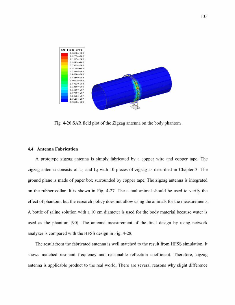
135
Fig. 4-26 SAR field plot of the Zigzag antenna on the body phantom
4.4 Antenna Fabrication
A prototype zigzag antenna is simply fabricated by a copper wire and copper tape. The
zigzag antenna consists of L1 and L2 with 10 pieces of zigzag as described in Chapter 3. The
ground plane is made of paper box surrounded by copper tape. The zigzag antenna is integrated
on the rubber collar. It is shown in Fig. 4-27. The actual animal should be used to verify the
effect of phantom, but the research policy does not allow using the animals for the measurements.
A bottle of saline solution with a 10 cm diameter is used for the body material because water is
used as the phantom [90]. The antenna measurement of the final design by using network
analyzer is compared with the HFSS design in Fig. 4-28.
The result from the fabricated antenna is well matched to the result from HFSS simulation. It
shows matched resonant frequency and reasonable reflection coefficient. Therefore, zigzag
antenna is applicable product to the real world. There are several reasons why slight difference

136
between the simulation and fabrication results exists. There are differences of the relative
permittivity and conductivity between the simulation and actual saline solution. Another possible
reason is slight difference of diameter and material characteristics of copper between the
simulation and l fabrication.
Fig. 4-27 Curved zigzag antenna with collar
Fig. 4-28 Comparison of HFSS models and curved zigzag antenna with collar, phantom,
tuning part, and shorting pin
50 100 150 200 250 300-35
-30
-25
-20
-15
-10
-5
0
Frequency, MHz
Refl
ecti
on
Co
eff
icie
nt,
dB
HFSS ResultMeasurement Result

137
CHAPTER 5 CONCLUSIONS
Three RF structures operating at different frequencies are analyzed with a full wave
electromagnetic simulator. The dissertation describes model structure, design challenges,
modeling strategy, design process, and results analysis. The full wave simulator used for the
whole modeling process demonstrates a great performance with the matched simulation results to
the references. The following sections will conclude the achieved work on the three antenna
structures and will propose possible extension to this work.
5.1 Completed Works
The completed works in this dissertation include:
1. The full wave EM simulators such FDTD and FEM are verified as useful tools by the
comparison of the NW and BNW modeling to the practical references. The setup of
accurate material characteristics and appropriate boundary conditions are significant
design issues. A full wave EM simulator is used for NW design and creates well-matched
results. The full wave EM simulation model of BNW with perfect regularity shows small
difference from the measurement due to the high irregularity of the practical fabrication of
branches. The HFSS simulation result of different directions of branches verifies the error
from irregularity problem.
2. The single on-chip antenna for MCMC system is a starting point of the wireless
communication of MCMC system. Two element array on-chip antenna enhances the

138
directional gain. Four element array antenna is introduced to create enhanced
reconfigurable gain patterns to 8 directions. The gains of two suggested orientations are
compared to find an appropriate combination of array antenna creating the maximum
enhancement of the gain. The star shape orientation is selected due to its stronger
combined gain. The separation factor resulting in the maximum combined gain is
determined by the array factor equation from Balanis’s Antenna theory book [66]. The
initial dimensions of AMC layer and antenna shows mismatched input impedance at 60
GHz because of the interaction between the four antennas and patches. The dimensions of
the patch and the antenna are tuned to result in the input impedance matching and
reasonable gain at 60 GHz. Two major performance matrices, PRE and budget are plotted
to evaluate the optimized antenna design.
3. The input impedance analysis of the antenna modification from monopole to zigzag
antenna demonstrates the effects of meandering and proximity to the body phantom. The
meandering creates the capacitive input impedance and shifts the resonant frequency up
while the body phantom with high dielectric constant shirts the resonant frequency down
due to the reduced phase velocity. The zigzag antenna analysis in terms of current
distribution from the bottom to the top of antenna describes the behavior of shorting pin.
The SAR simulation result proves the effect of zigzag antenna to the lives is safe enough.
The return loss of simulation result is compared to the actual fabrication measurement and
the results are well-matched.

139
5.2 Future Works
The simulation result of the BNW modeling with perfect regularity supports an idea of the
substrate result to the measurement of the practical model, but it is improper to predict the
accurate result. The BNW model more close to the realistic solar substrate with a proper degree
of irregularity is needed to create more accurate reflectivity. Fig. 5.1 shows the irregular
branched NW.
Fig. 5-1 Irregular branched NW

140
The simulation model of the four element array antenna is fed with the waveports located
between the antenna package and silicon substrate as shown in Fig 5.2. However, it is not proper
method of feeding in the practical design. The appropriate feeding method for the four element
array antenna is required for the actual fabrication since the waveport is impractical in the actual
antenna fabrication.
Fig. 5-2 Waveport feeding antenna package
The milti-line multi-layer (MLML) zigzag antenna that is applied to the small animals such
as house cats or tamarins is suggested by the senior design teams of the University of Arizona, as
shown in Fig. 5-3. The MLML zigzag design has higher coupling capacitance due to more pieces
of zigzag and overlapped antenna layer. The input impedance analysis of the MLML zigzag
antenna is a proper future work of the zigzag antenna research.
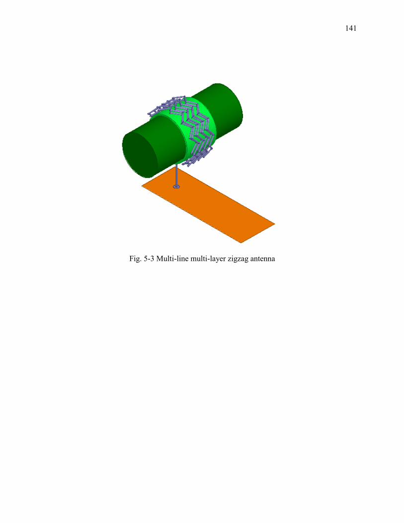
141
Fig. 5-3 Multi-line multi-layer zigzag antenna

142
APPENDIX A ANOTHER APPROACH OF SEPARATION FACTOR
(a) (b)
Fig. A-1 Four element antennas array in the spherical coordinate system of (a) ring (b) star
[
| |
| |
| |
| |
| |
| |
| |
| |]
=90˚ (A.3)
Table A.1 Antenna feeding point positions
| |
√
| | √
| | √
X, =0
Y =90
X, =0
Y =90
B
A
B
A
C
D
C
D
Axis \ Elements A B C D
X 0 0
Y 0 0
-
-

143
| | √
| | | | | | | | | |
| |[ (
√ ) (
√ ) (
√ ) (
√ )]
Fig. A-2 Array factor plots along to the distance between the antenna feeding points
0 0.5 1 1.5 2 2.5 3 3.5 4 4.5 50
0.5
1
1.5
2
2.5
distance, mm
AF
phi = 45, 225
phi = 135, 315

144
REFERENCES
[1] R. L. Smith-Rose, “Radio-Wave Propagation Research in the Department of Scientific and
Industrial Research during the Years 1937-46” Electrical Engineers-Part III:
Radiocommunication, Journal of the Institution of, vol. 94, no.16, pp. 879-892, March 1947.
[2] [Online]http://www.its.bldrdoc.gov/isart/bio/
[3] S. Yoo; K.L. Melde, "VHF Collar Integrated Antenna for Ground Link of GPS Based
Location System," Antennas and Propagation, IEEE Transactions on , vol. 61, no.1, pp. 26-
32, Jan. 2013.
[4] [Online]http://ourfiniteworld.com/2012/07/26/an-optimistic-energygdp-forecast-to-2050-
based-on-data-since-1820/
[5] [Online]http://www.globalwarmingart.com/wiki/File:Global_Carbon_Emission_by_Type
png
[6] National Center for Photovoltaics [Online]http://www.nrel.gov/ncpv
[7] B. . Kayes and H. A. Atwater, “Comparison of the device physics principles of planar and
radial p-n junction nanorod solar cells,” J. of Appl. Phys. vol , 97, no. 11, 2005.
[8] T. J. Brockett, H. Rajagopalan, R. B. Laghumavarapu, D. Hufakker, and Y. Rahmat-Samii,
“Electromagnetic Characterization of High Absorption Sub-Wavelength Optical
Nanostructure Photovoltaics for Solar Energy Harvesting,” IEEE Trans. On Antennas and
Propagation, vol. 61, no. 4, April 2013.
[9] International Technology Roadmap for Semiconductors, 2012 Edition, [Online]:
http://www.itrs.net/
[10] J. M. Rabaey, A. Chandrakasan, and B. Nikolic, Digital Integrated Circuits: A Design
Perspective , 2nd Edition., Prentice Hall, 2003.
[11] J. L. Hennessy and D. A. Patterson, Computer Architecture: A Quantitative Approach, 4th
Edition., Elsevier, 2006.
[12] R. E. Collin, Foundations for microwave engineering, McGraw-Hill, New York 1992
[13] H.-H. Yeh, “Developments of 60 ghz antenna and wireless interconnect inside multi-chip
module for parallel processor system,” Ph.D. dissertation, Dept. Elect. Eng., Univ. of
Arizona., Tucson, AZ, 2013.

145
[14] H.-H. Yeh, N. Hiramatsu, K. L. elde, “The Design of Broadband 60 GHz AMC Antenna in
Multi-Chip RF Data Transmission,” IEEE Transactions on Antenna and Propagation, vol. 61,
no. 4, Apr. 2013.
[15] J. C. G. atthews, B. Pirollo, A. Tyler, and G.Pettitt, “Body Wearable Antennas for
UHF/VHF,” Loughborough Antennas and Propagation Conference, pp.357-360, March 2008
[16] Tritronics [Online]http://www.tritronics.com
[17] Firestik [Online]http://www.firestik.com/Tech_Docs/murs.htm
[18] B. Rech and H. Wagner, “Potential of amorphous silicon for solar cells,” Appl. Phys. A vol
69, pp.155-167, 1999.
[19] X. Deing and E. A. Schiff, “Amorphous Silicon-based Solar Cells,” Handbook of
Photovoltaic Science and Engineering, 2002.
[20] Y. Cui et. al, “Optical Absorption Enhancement in Amorphous Silicon Nanowire and
Nanocone Arrays” Nano Lett. vol. 9, No. 1, 2009.
[21] . A. Green, “Self-consistent optical parameters of intrinsic silicon at 300 including
temperature coefficients,” Solar energy material & solar cells, vol. 92, pp. 1305-1310, 2008.
[22] [Online]http://refractiveindex.info/
[23] Reference Solar Irradiance [Online]http://rredc.nrel.gov/solar/spectra/am1.5/#c
[24] H. C. Casey, Jr., “Devices for Integrated Circuits,” John Wiley & Sons, Inc, NJ, 1998.
[25] Y. Taur and T. K. Ning, Fundamentals of Modern VLSI Devices, Cambridge University Press,
NY, 1998.
[26] D. M.Pozar, Microwave Engineering, 3rd. Danvers, MA: Wiley 2005.
[27] PVCDROM [Online]http://pveducation.org/pvcdrom
[28] C. H. Crouch, J. E. Carey, J. M. Warrender, M. J. Aziz, and E. Mazur, "Comparison of
structure and properties of femtosecond and nanosecond laser-structured silicons," Applied
Physics Letters, vol. 84, no. 11 pp. 1850-1852, 2004.
[29] B. . Kayes and H. A. Atwater, “Comparison of the device physics principles of planar and
radial p-n junction nanorod solar cells,” J. of Appl. Phys. Vol 97, p 114302, 2005.
[30] . J. Bierman, S. Jin, “Potential applications of hierarchical branching nanowires in solar
energy conversion,” Energy Environ. Sci., Jul. 2009.

146
[31] L. L. Kazmerski, “Solar photovoltaics R&D at the tipping point: A 2005 technology
overview,”J. Electron Spectroscopy and Related Phenomena vol. 150, no 2-3, pp. 105-135,
Feb. 2006.
[32] B. . Kayes, H.A. Atwater and N.S. Lewis, “Comparison of the device physics principles of
planar and radial p-n junction nanorod solar cells,” J. Appl. Phys. vol. 97, no. 11, p. 114302,
Mar. 2005.
[33] B. M. Kayes, Radial pn Junction, Wire Array Solar Cells, Ph.D. Thesis, California Institute
of Technology, 2009. (Thesis)
[34] H.P. Yoon, Y. Yuwen, C.E. Kendrick, G.D. Barber, N.J. Podraza, J.M. Redwing, T.E.
Mallouk, C.R. Wronski and T.S. Mayer, “Enhanced conversion efficiencies for pillar array
solar cells fabrication from crystalline silicon with short minority carrier diffusion lengths,”
Appl. Phys. Lett. 96, p. 213503, May 2010.
[35] M. Kelzenberg, S. Boettcher, J. Petykiewics, D. Turner-Evans, M. Putnam, E. Warren. J.
Spurgeon, R. Briggs, N. Lewis, H. Atwater, “Enhanced absorption and carrier collection of
Si wire arrays for photovoltaic applications,” Nature Materials, Feb 2010, pp. 239-244.
[36] L.Y. Cao, P. Fan, A.P. Vasudev, J.S. White, Z. Yu, W. Cai, J.A. Schuller, S. Fan and M.L.
Brongersma, “Semiconductor nanowire optical antenna solar absorbers,” Nano Lett., vol. 10,
no. 2, pp. 439-445, Jan. 2010.
[37] W. F. Liu, J. I. Oh, and W. Z. Shen, “Light trapping in single coaxial nanowires for
photovoltaic applications,” IEEE Electron Device Letters, vol. 32, no. 1, pp. 45-47, Jan. 2011.
[38] O. L. Muskens, J. G. Rivas, R. E. Algra, E. P. A. . Bakkers, and A. Lagendijk, “Design of
light scattering in nanowire materials for photovoltaic applications,” Nano Lett., vol. 8, no. 9,
pp. 2638-2642, Aug. 2008.
[39] H. Rajagopalan, T. Brockett, and Y. Rahmat-Samii, “Investigation of semiconductor
nanostructures photovoltaics for next generation solar cells,” 2011 IEEE Antennas and
Propagation (APSURSI), pp. 1089-1091, July 2011.
[40] G. Chen and L. Hu, “Silicon Nanowires for solar photovoltaic applications,” SPIE Newsroom,
p. 1087, Aug. 2008.
[41] L. Hu and G. Chen, “Analysis of optical absorption in silicon nanowire arrays for
photovoltaic applications,” Nano Lett. vol. 7, no. 11, pp. 3249-3252, 2007
[42] R. S. Wagner and W.C. Ellis, “Vapor-liquid-solid mechanism of single crystal growth,” Appl.
Phys. Lett. 4, vol. 4, no. 5, pp. 89-90, Feb. 1964.

147
[43] C. A. Balanis, Advanced engineering electromagnetism, John Wiley & Sons, Inc, NJ, 1989
[44] J. Kupac and B.Wotzogman, “Computational electromagnetics for nanowire solar cells,” J.
Comput. Electron vol. 11, no. 153, 2012
[45] C. Lundgren, “FDTD modeling of solar energy absorption in Si branched nanowires,” Optics
Express vol. 21, A392, 2013
[46] O. Isabella, S. Solntsev, D. Caratelli, and . Zeman, “3-D optical modeling of thin-film Si
solar cells on diffraction gratings,” Progress in Photovoltaics: Research and Applications vol.
21, no. 94 2013
[47] P. W. Hannan and M. A. Balfour, “Simulation of a phased-array antenna in waveguide,”
IEEE Trans. On Antenna and Propagation, vol. 13, May 1965.
[48] T. Itoh, G. Pelosi, P. P. Silvester, Finite Element Software for Microwave Engineering, John
Wiley & Sons, Inc, NJ, 1996
[49] R. A. Street, Hydrogenated Amorphous Silicon, Cambridge University Press, NY, 2005.
[50] HFSS V.15, Ansys Corporation [Online] www.ansys.com
[51] C. Kendrick, C. Di arino, S. Yoo, K. L. elde, and Joan Redwing, “Growth and Optical
Analysis of Branching Silicon Wire Array,”
[52] Y. P. Zhang and D. Liu, “Antenna-on-Chip and Antenna-in-Package Solutions to Highly
Integrated Millimeter-Wave Devices for Wireless Communications,” IEEE Trans. Antenna
and Propagation., vol. 57, No. 10, pp. 2830-2841, Oct. 2009.
[53] H.-T. Wu, . Tekle, C. S. Nallani, N. Zhang, and K. K. O, “Bondwire Antenna/Feed for
Operation near 60 GHz,” IEEE Trans. Microwave Theory and Tech., vol. 57, no. 12, pp.
2966-2972, Dec. 2009.
[54] D. Liu, J. A. G. Akkermans, H.-C. Chen, and B. Floyd, “Packages with Integrated 60-GHz
Aperture-Coupled Patch Antennas,” IEEE Trans. Antennas Propag and Propagation., vol.
59, no. 10, pp.3607-3616, Oct. 2011.
[55] F. Yang, A. Aminian, and Y. Rahmat-Samii, “A novel surface-wave antenna design using a
thin-periodically loaded ground plane,” Microwave and Optical Technology Letters, vol. 47,
no. 3, pp. 240-245, Nov. 2005.
148
[56] D. Sievenpiper, L. Zhang, R. F. J. Broas, N. G. Alexopolous, and E. Yablonovitch, “High-
impedance electromagnetic surfaces with a forbidden frequency band,” IEEE Transaction on
Microwave Theory and Techniques, vol. 47, no. 11, pp. 2059–2074, Nov. 1999.
[57] N.Hiramatsu, “Analysis and design of low-profile antennas over an artificial magnetic
conductor for inter-core communications,” Ph.D. dissertation, Dept. Elect. Eng., Univ. of
Arizona., Tucson, AZ, 2011.
[58] F. Yang and Y. Rahmat-Samii, “Reflection phase characterizations of the EBG ground plane
for low profile wire antenna applications,” IEEE Transactions on Antennas and Propagation,
vol. 51, no. 10, pp. 2691-2703, Oct. 2003.
[59] [Rogers 3003C Laminates Manual, Rogers Corporation., [Online]
http://www.rogerscorp.com/.
[60] H.-H. Yeh, N. Hiramatsu, K. L. elde, “Wireless RF Data Communications Using 60 GHz
Antennas in Multi-Core Systems,” in IEEE Proc. on EPEPs, Oct. 2011.
[61] H.-H. Yeh, K. L. elde, “Developments of 60 GHz Wireless Interconnects for Parallelized
Multi-Processor Computing,” IEEE Transactions on Components, Packaging and
Manufacturing Technology, vol. 3, no. 11, Nov. 2013.
[62] H.-H. Yeh, K. L. elde, “Design and Packaging of 60 GHz Antenna Array for ulti-Chip
Communication,” in IEEE International Conference on Wireless Information Technology
and Systems (ICWITS), Nov. 2012.
[63] Rogers 4003C Laminates Manual, Rogers Corporation., [Online]. Available:
http://www.rogerscorp.com/.
[64] S.-S. Hsu, K.-C. Wei, C.-Y. Hsu, and H. Ru-Chuang, “A 60-GHz Millimeter-Wave CPW-
Fed Yagi Antenna Fabricated by Using 0.18-µm C OS Technology,” IEEE Electron Device,
Letters, vol. 29, no. 6, pp.625-627, June. 2008.
[65] H.-T. Wu, . Tekle, C. S. Nallani, N. Zhang, and K. K. O, “Bondwire Antenna/Feed for
Operation near 60 GHz,” IEEE Trans. Microwave Theory and Tech., vol. 57, no. 12, pp.
2966-2972, Dec. 2009.
[66] C.A. Balanis, Antenna Theory: Analysis and Design, 3rd
Edition, John Wiley & Sons, Inc.,
New Jersey, 2005
[67] J. T. Bernhard, R. Wang, R. Clark, and P. Mayes, “Stacked reconfigurable antenna elements
for space based radar applications,” in Proc. IEEE/URSI Antennas Propagat. Soc. Int. Symp.,
vol. 1, 2001, pp.158–161.

149
[68] W. H. Weedon, W. J. Payne, and G. . Rebeiz, “ E S-switched reconfigurableantennas,”
in Proc. IEEE Int. Symp. Antennas Propagat.,vol. 3, 2001, pp. 654–657.
[69] R. N. Simons, C. Donghoon, and L. P. B. Katehi, “Reconfigurable array antenna using
microelectromechanical systems ( E S) actuators,” in Proc. IEEE Int. Symp Antennas
Propagat., vol. 3, 2001, pp. 674–677.
[70] G.H. Huff, J. Feng, S. Zhang , and J. T. Bernhard, “A Novel Radiation Pattern and Frequency
Reconfigurable Single Turn Square Spiral icrostrip Antenna,” IEEE Microwave Wireless
Components Lett. vol. 13 pp. 57-59, Feb. 2003.
[71] D. Rodrigo, Y. Damgaci, N. Biyikli, B. A. Cetiner, J. Romeu, and L. Jofre, “ E S-
reconfigurable antenna based on a multi-size pixelled geometry,” in Proc. 4th Eur. Conf.
Antennas and Propagation (EuCAP), 2010, pp. 1–4.
[72] J. C. G. Matthews, B. Pirollo, A. Tyler, and G. Pettitt,” Body Wearable Antennas for
UHF/VHF,” Loughborough Antennas and Propagation Conference, pp.357-360, 2008.
[73] R. L. Smith-Rose, “Radio-Wave Propagation Research in the Department of Scientific and
Industrial Research during the Years 1937-46,” Electrical Engineers-Part III:
Radiocommunication, Journal of the Institution of, vol. 94, no. 16 pp. 879-892, 1947.
[74] National Telecommunications & Information Administration. Institute for
Telecommunication Science, Boulder, CO [Online]http://www.its.bldrdoc.gov/isart/
[75] National Telecommunications & Information Administration. United States Department of
Commerce [Online]http://www.ntia.doc.gov
[76] Firestik, http://www.firestik.com/Tech_Docs/murs.htm
[77] S. H. Lee and K.K. Mei, “Analysis of zigzag antennas, ” IEEE Trans. on Antenna and
Propagation, vol. 18, no. 6, pp.760-764, 1970.
[78] D.L. Sengupta,” The Radiation Characteristics of a Zig-Zag Antenna,” IRE Trans. On
Antenna and Propagation, pp.191-194, 1958.
[79] S. H. Zainud-Deen, K. H. Awadalla, A.I. Bahnacy, and H.A. Sharshar, “ Performance
analysis of zigzag antenna for portable radio equipment,” IEEE Antenna and Paopagation
Society International Symposium, 1, pp.442-445, 1997.
[80] Oracle [Online]http://library.thinkquest.org/3500/polarbear.htm
[81] The IUCN Red List of Threatened Species [Online] http://www.iucnredlist.org

150
[82] Wikipedia [Online]www.wikipedia.com
[83] T. Sunaga, H. Ikehira, S. Furukawa, H. Shinkai, H. Kobayashi, Y. Matsumoto, E. Yoshitome,
T. Obata, S. Tanada, H. urata, and Y. Sasaki, “ easurement of the electrical properties of
human skin and the variation among subjects with certain skin conditions,” Phys. Mde. Biol.
vol. 47, pp.N11-N15, 2002.
[84] N. Haga, K. Saito, . Takahashi, and K. Ito, “Characteristics of Cavity Slot Antenna for
Body-Area Networks,” IEEE trans.On Antennas and Propagation, vol. 57, no. 4, pp.837-843,
April 2009.
[85] H. A. Wheeler, “The radiansphere around a small antenna,” Proc. IRE, vol. 47, no. 8, pp.
1325–1331, 1959.
[86] J. . artine, G. W. Swenson, and J. T. Bernhard, “ ethodology for efficiency
measurement of electrically small monopoles for animal tracking,” IEEE antenna Propag.
Mag., vol. 51, no. 2, pp.39-47, April 2009.
[87] T. M. Vu, A. Diallo, C. Luxey, G. Kossiavas , "Optimization of the Size and the Shape of a
Wheeler Cap for Mobile Phone-Antenna Efficiency Measurements," Antennas and
Propagation, EuCAP 2007. The 2nd European Conference on , pp.1-6, 11-16, Nov. 2007.
[88] T. Salim and P. S. Hall, “Efficiency measurement of antennas for on-body communications,”
Microw. Opt. Technol. Lett., vol. 48, no. 11, Aug. 2006.
[89] J. H. Kim and H. . Lee, “Low specific absorption rate wearable antenna for WLAN band
application,” Antennas and Propagation, 2010 Proceedings of the Fourth European
Conference on , pp. 12-16 April 2010.
[90] S. J. Allen, “ easurement of power absorption by human phantoms immersed in radio-
frequency field,” Biologic Effects of Nonionizing Radiation, pp. 494-498, Feb. 1975.


