

AUTHOR
Anira Binti Abdul Rashid
Siti Mariam Binti Hussain
Gauri A/p Birasamy
ELECTRICAL Engineering department

i
AUTHOR
Anira Binti Abdul Rashid Siti Mariam Binti Hussain Gauri A/p Birasamy
Copyright © 2021.
All rights reserved. No part of this publication may be reproduced, distributed, or transmitted in any form or by any means, including photocopying, recording, or other electronic or mechanical methods, without the prior written permission of the publisher, except in the case of brief quotations embodied in critical reviews and certain other noncommercial uses permitted by copyright law. For permission requests, write to the publisher at the address below.
ISBN: 9789670855769
Politeknik Tuanku Sultanah Bahiyah (PTSB)
Kulim Hi-Tech Park,
09090 Kulim, Kedah.
https://ptsb.mypolycc.edu.my
ELECTRONIC CIRCUITS WORKBOOK
USING MULTISIM ONLINE
SIMULATOR STUDENT GUIDE EDITION

ii
hanks to our family and colleagues at Electrical Engineering Department, Politeknik Tuanku Sultanah Bahiyah for being the support team to complete this e-book. Last but not least we also thank you to the “PTSB Team E- Book” and technical team for guiding us in completing this e-book.
T
iii
PREFACE
Electronic Circuits Workbook using multisim online simulator is our special present for students who are studying Electronic Circuits course as well as all the lecturers involve. It provides guidance for students to do their practical lab by using multisim online simulator. There are 6 chapters covered in this e-book which is Bridge Rectifier Circuit, Oscillator, Operational Amplifier, Astable Multivibrator, Filter and Analog to Digital or Digital to Analog Converter. In this e- book will present valuable information with supporting diagrams to help students more understanding in doing their practical laboratory. Finally, we hope this book will benefit all those seeking knowledge on this subject and will help in understanding electronic circuits better.

iv
INTRODUCTION 1 UNIT 1 : BRIDGE RECTIFIER CIRCUIT 2
1.1 THEORY 2 1.2 PRACTICAL OF BRIDGE RECTIFIER 6 1.3 QUESTION 8
UNIT 2 : COLPITTS OSCILLATOR CIRCUIT 9
2.1 THEORY 9 2.2 PRACTICAL OF COLPITS OSCILLATOR CIRCUITS 11 2.3 QUESTION 14
UNIT 3 : OPERATIONAL AMPLIFIER 15
3.1 THEORY 15 3.2 PRACTICAL OF NON-INVERTING AMPLIFIER 16 3.3 QUESTION 22 UNIT 4 : ASTABLE MULTIVIBRATOR 23
4.1 THEORY 23 4.2 PRACTICAL OF ASTABLE MULTIVIBRATOR USING TIMER (555) IC 26 4.3 QUESTION 30
UNIT 5 : LOW PASS FILTER 31
5.1 THEORY 31 5.2 PRACTICAL LABORATORY 33 5.3 QUESTION 36 5.4 EXERCISES 36
UNIT 6 : DIGITAL TO ANALOG CONVERTER 37
6.1 THEORY 37 6.2 PRACTICAL LABORATORY 38 6.3 QUESTION 41
ANSWERS 43 REFERENCES 60

1
NI Multisim (formerly MultiSIM) is an electronic
schematic capture and simulation program which
is part of a suite of circuit design programs, along
with NI Ultiboard. Multisim is widely used in
academia and industry for circuits education,
electronic schematic design and SPICE simulation.
Multisim™ software provides SPICE simulation,
analysis, and printed circuit board (PCB) tools to
help you quickly iterate through designs and
improve prototype performance. Move from
schematic to layout seamlessly to save time and
reduce prototype iterations.
https://www.instructables.com/How-to-Use-Multisim-Live/
INTRODUCTION

2
BRIDGE RECTIFIER CIRCUIT
1.1 INTRODUCTION
Direct Current (DC) power supply units in electronic components will be used to convert Alternating
Current (AC) voltage to DC voltage. Figure 1.1 show the block diagram and correspond output from each
power supply block. The character of the output voltage from power supply is almost same as DC voltage
supplied by a battery.
BLOCK DIAGRAM AND FUNCTION EACH UNIT
Figure 1.1: Block diagram of Power supply and output waveform for each block
• Transformer - Reduce the value of the input ac voltage.
• Rectifier - A circuit that converts ac voltage to pulsating dc voltage.
• Filter - The main task of filter is to convert the voltage at pulse to the voltage rippled.
• Voltage Regulator - To stabilize the pure DC voltage (at the output of the filter).
• Voltage Divider - Circuit is needed in power supplies for electric equipment requires.
Rectifier is the main circuit converting the AC voltage to DC voltage. It is divide into three types. Half-wave
rectifier, Full-wave rectifier and Bridge rectifier. Bridge rectifier is consisting of four individual diode
Transformer Rectifier Voltage
Regulator
Voltage
Divider
Filter VDC VAC
UNIT 1

3
connected in a closed loop and produce full wave DC voltage provides the same polarity of output voltage
for either polarity of input voltage.
(a) (b)
Figure 1.2: (a)Component and (b) Circuit of Bridge rectifier
Typical applications Bridge Rectifier are:
i) Welding- to supply polarized voltage for welding. In such circuits control of the output
current is required and this is sometimes achieved by replacing some of the diodes in bridge
rectifier with thyristor, whose voltage output can be regulated by means of phase fired
controllers.
ii) Generator
iii) Battery charger
iv) AC motor drive
v) Traction markets
vi) Detection of amplitude modulated radio signals
ELECTRONIC CIRCUITS WORKBOOK USING MULTISIM ONLINE SIMULATOR
S T U D E N T G U I D E E D I T I O N
4
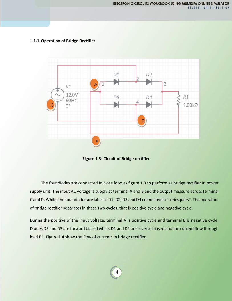
1.1.1 Operation of Bridge Rectifier
Figure 1.3: Circuit of Bridge rectifier
The four diodes are connected in close loop as figure 1.3 to perform as bridge rectifier in power
supply unit. The input AC voltage is supply at terminal A and B and the output measure across terminal
C and D. While, the four diodes are label as D1, D2, D3 and D4 connected in “series pairs”. The operation
of bridge rectifier separates in these two cycles, that is positive cycle and negative cycle.
During the positive of the input voltage, terminal A is positive cycle and terminal B is negative cycle.
Diodes D2 and D3 are forward biased while, D1 and D4 are reverse biased and the current flow through
load R1. Figure 1.4 show the flow of currents in bridge rectifier.
A
A
B
A
C
D
ELECTRONIC CIRCUITS WORKBOOK USING MULTISIM ONLINE SIMULATOR
S T U D E N T G U I D E E D I T I O N

5
(a) (b)
Figure 1.4: Flow of the currents (a) Positive half cycle and (b) Negative half cycle
When the negative of the input voltage, terminal B is positive cycle and terminal A is negative
cycle. Diodes D1 and D4 are forward biased while, D2 and D3 are reverse biased and the current flow
through load R1. Since the direction current flow through R1 is similar to the current flow through the
positive cycles, so similar wave will produce.
Figure 1.5: Output at R1
ELECTRONIC CIRCUITS WORKBOOK USING MULTISIM ONLINE SIMULATOR
S T U D E N T G U I D E E D I T I O N
6
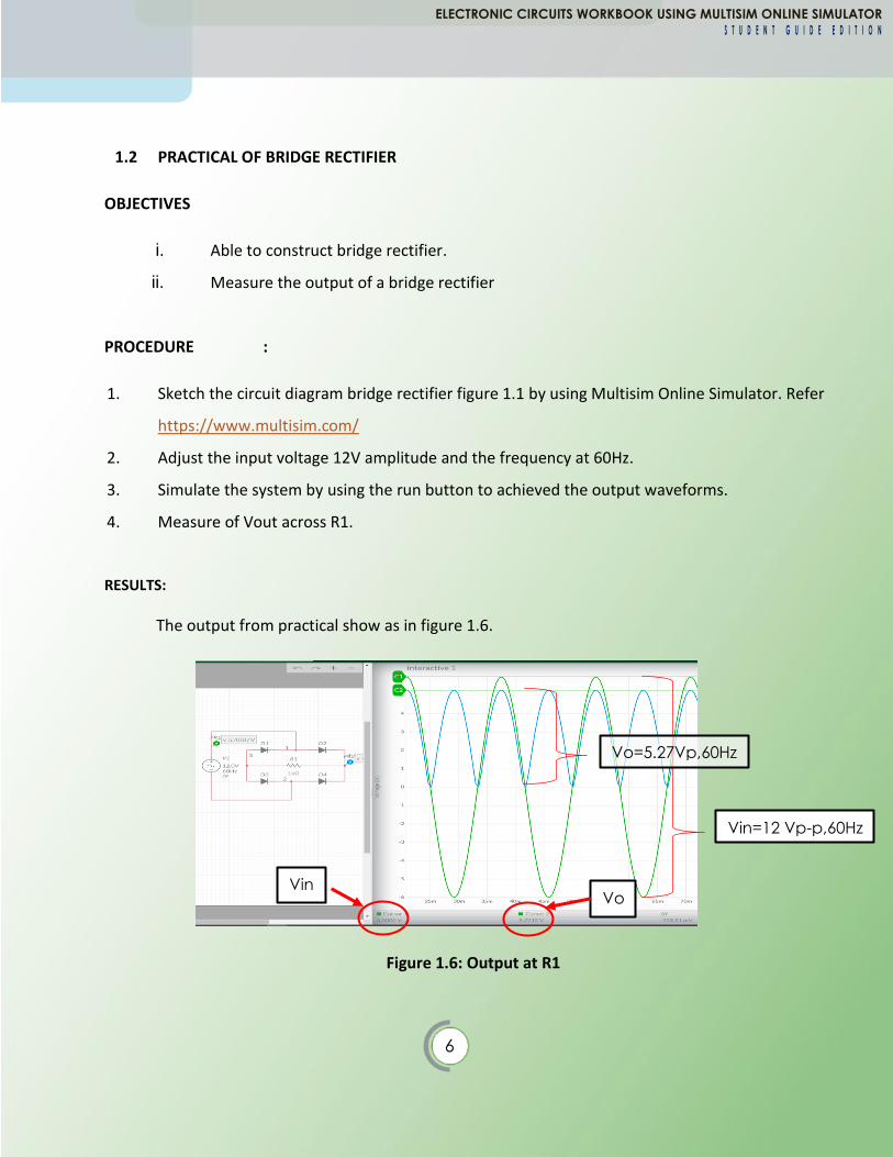
1.2 PRACTICAL OF BRIDGE RECTIFIER
OBJECTIVES
i. Able to construct bridge rectifier.
ii. Measure the output of a bridge rectifier
PROCEDURE :
1. Sketch the circuit diagram bridge rectifier figure 1.1 by using Multisim Online Simulator. Refer
https://www.multisim.com/
2. Adjust the input voltage 12V amplitude and the frequency at 60Hz.
3. Simulate the system by using the run button to achieved the output waveforms.
4. Measure of Vout across R1.
RESULTS:
The output from practical show as in figure 1.6.
Figure 1.6: Output at R1
Vin=12 Vp-p,60Hz
Vo=5.27Vp,60Hz
Vin Vo
ELECTRONIC CIRCUITS WORKBOOK USING MULTISIM ONLINE SIMULATOR
S T U D E N T G U I D E E D I T I O N

7
*Hint: There is a different between Vin and Vo cause by the types of diode use. Since current across
the diode at one cycle and voltage drop at diode is 0.7V (assumed 2 germanium diode), voltage drop
is Vo = Vin - 0.7V
1.3 QUESTION
1. Determine the output(Vo) across RL in Figure 1.7.
Figure 1.7: Output at RL
2. If the diode at figure 1.7 change from germanium diode to silicon diode, calculate the Vo across
RL.
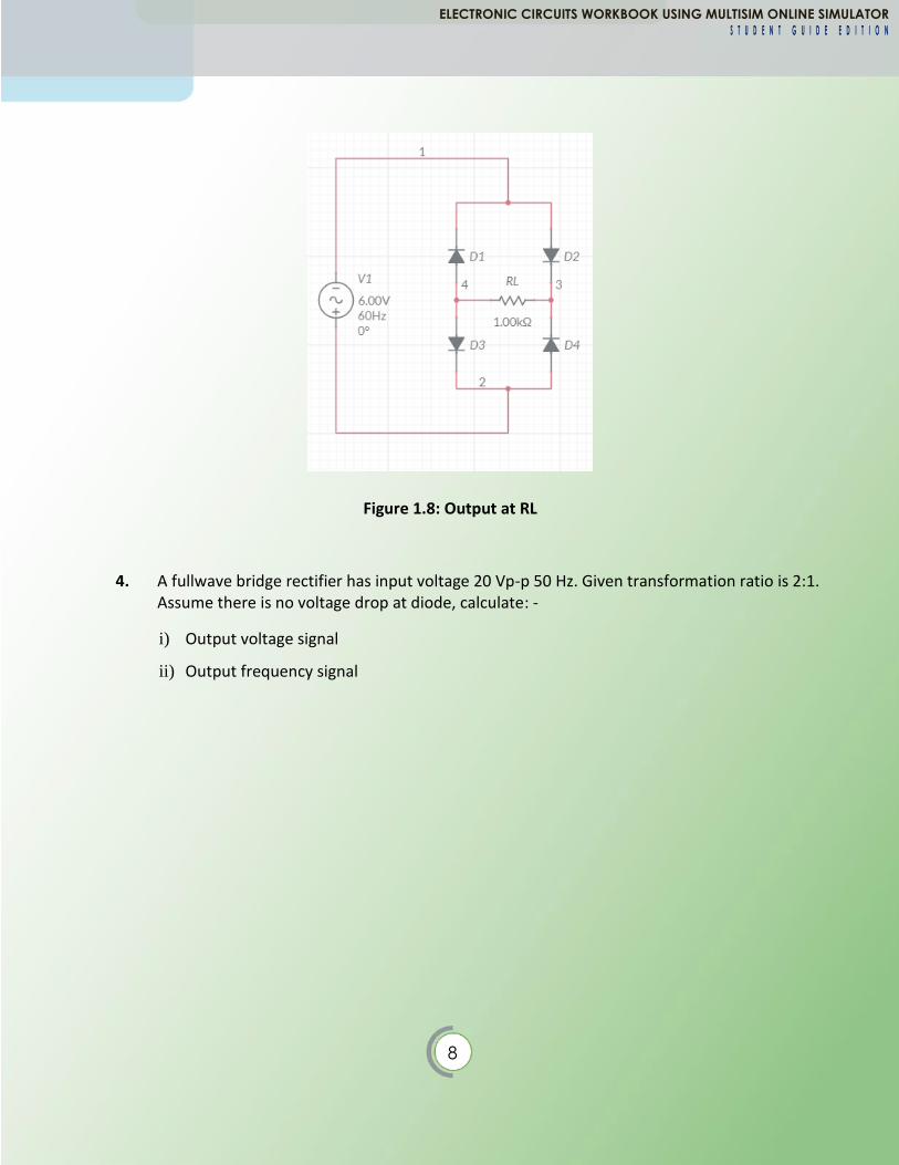
3. Measure the output(Vo) across RL and calculate the Vo in Figure 1.8.
ELECTRONIC CIRCUITS WORKBOOK USING MULTISIM ONLINE SIMULATOR
S T U D E N T G U I D E E D I T I O N
8
Figure 1.8: Output at RL
4. A fullwave bridge rectifier has input voltage 20 Vp-p 50 Hz. Given transformation ratio is 2:1. Assume there is no voltage drop at diode, calculate: -
i) Output voltage signal
ii) Output frequency signal
ELECTRONIC CIRCUITS WORKBOOK USING MULTISIM ONLINE SIMULATOR
S T U D E N T G U I D E E D I T I O N

9
COLPITTS OSCILLATOR CIRCUIT
2.1 THEORY
Oscillator is the source of basic signal generator for multi-application in the electronic circuit. It
will change the DC voltage into AC signal and be able to generate any frequency value needs by the
circuit.
All basic oscillator circuit consist 3 parts like amplifier, feedback circuit and frequency generator circuit
In the Colpitts circuit, two capacitors and one inductor determine the frequency of oscillation.
The feedback needed for oscillation is taken from a voltage divider made by the two capacitors. The
Colpitts Oscillator has fairly good frequency stability, is easy to tune, and can be used for a wide range
of frequencies. The large value of split capacitance is in parallel with the junctions and minimizes the
effect on frequency stability.
Output Amplifier
Feedback Frequency
Generator
Circuit
Figure 2.1: Block diagram of an Oscillator circuit
UNIT 2

10
The frequency of oscillations for a Colpitts Oscillator is determined by the resonant frequency of the LC
tank circuit and is given as:
where CT is the capacitance of C1 and C2 connected in series and is given as:
Advantages of Colpitts oscillator Main advantage of Colpitts oscillator over Hartley oscilator is the better performance in the high frequency
state. This is because the capacitors offer a low reactance path for the high frequency signals and thus the
output signals in the high frequency domain will be more sinusoidal. Due to the excellent performance in
the high state, the Colpitts oscillator can be even used in microwave uses.
ELECTRONIC CIRCUITS WORKBOOK USING MULTISIM ONLINE SIMULATOR
S T U D E N T G U I D E E D I T I O N

11
2.2 PRACTICAL OF COLPITS OSCILLATOR CIRCUIT
OBJECTIVES
i) Able to construct oscillator circuit.
ii) Able to determine the oscillation frequency by using the formula and the effect of varying
the values of the L and C to the oscillation frequency.
iii) Sketch the output waveform of varying the values of the L and C to the oscillation
frequency.
PROCEDURE
Figure 2.2: Schematic of Colpitts Oscillator Circuit
1. Sketch the circuit diagram of figure 2.2 by using Multisim Online Simulator. Refer
https://www.multisim.com/
2. Simulate, draw and measure the output waveform to get output frequency. Compare that value
with the calculation value.
3. Change the value of L, and repeat procedure number 2.
ELECTRONIC CIRCUITS WORKBOOK USING MULTISIM ONLINE SIMULATOR
S T U D E N T G U I D E E D I T I O N

12
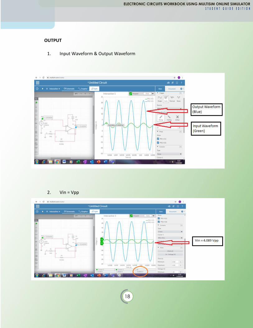
OUTPUT
1. Input Waveform & Output Waveform
2. L = 1mH
ELECTRONIC CIRCUITS WORKBOOK USING MULTISIM ONLINE SIMULATOR
S T U D E N T G U I D E E D I T I O N
13
Calculation of Output Frequency using formula :
𝐶𝑇 = 𝐶1𝑋𝐶2
𝐶1 + 𝐶2
𝐶𝑇 = 0.1µ𝑋0.1µ
0.1µ + 0.1µ= 50𝑛𝐹
𝑓𝑟 = 1
2𝜋√1𝑚 𝑥 50𝑛𝐹 = 22.5 kHz
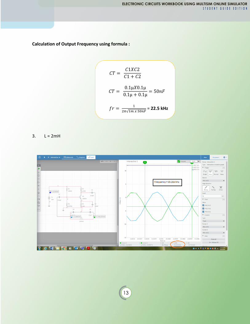
3. L = 2mH
ELECTRONIC CIRCUITS WORKBOOK USING MULTISIM ONLINE SIMULATOR
S T U D E N T G U I D E E D I T I O N
14
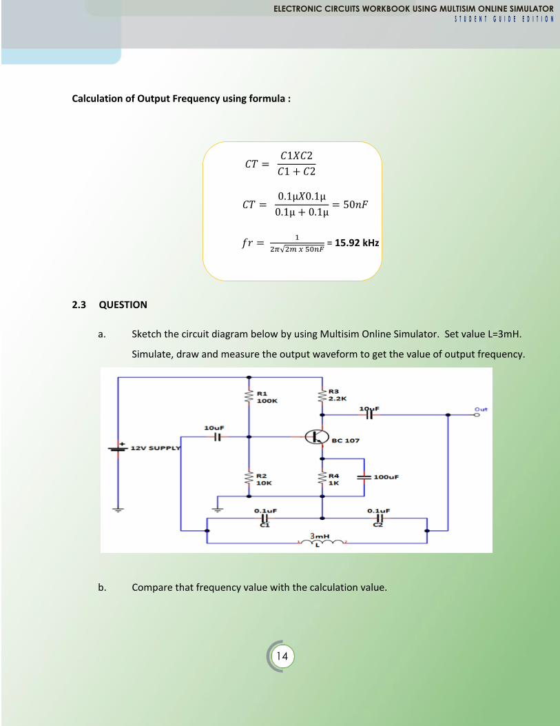
Calculation of Output Frequency using formula :
𝐶𝑇 = 𝐶1𝑋𝐶2
𝐶1 + 𝐶2
𝐶𝑇 = 0.1µ𝑋0.1µ
0.1µ + 0.1µ= 50𝑛𝐹
𝑓𝑟 = 1
2𝜋√2𝑚 𝑥 50𝑛𝐹 = 15.92 kHz
2.3 QUESTION
a. Sketch the circuit diagram below by using Multisim Online Simulator. Set value L=3mH.
Simulate, draw and measure the output waveform to get the value of output frequency.
b. Compare that frequency value with the calculation value.
ELECTRONIC CIRCUITS WORKBOOK USING MULTISIM ONLINE SIMULATOR
S T U D E N T G U I D E E D I T I O N
15
OPERATIONAL AMPLIFIER
3.1 THEORY
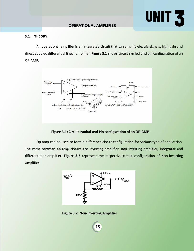
An operational amplifier is an integrated circuit that can amplify electric signals, high gain and
direct coupled differential linear amplifier. Figure 3.1 shows circuit symbol and pin configuration of an
OP-AMP.
Figure 3.1: Circuit symbol and Pin configuration of an OP-AMP
Op-amp can be used to form a difference circuit configuration for various type of application.
The most common op-amp circuits are inverting amplifier, non-inverting amplifier, integrator and
differentiator amplifier. Figure 3.2 represent the respective circuit configuration of Non-Inverting
Amplifier.
Figure 3.2: Non-Inverting Amplifier
UNIT 3

16
Close Loop Gain, 𝑨𝒄𝒍 = 𝟏 +𝑹𝒇
𝑹𝒊
Phase Angle, 𝜽 = 𝒕
𝑻 𝑿 𝟑𝟔𝟎°
The noninverting amplifier has much higher circuit input impedance. It does not produce an 180°
voltage phase shift from input to output; i.e., the input and output voltages are in phase. A noninverting
amplifier is shown in figure below
Figure 3.3: Non-Inverting Amplifier
3.2 PRACTICAL OF NON-INVERTING AMPLIFIER
OBJECTIVES
i. Able to construct op-amp circuit for Non-inverting amplifier.
ii. Determine the voltage gain (Av) or gain of closed loop (Acl).
iii. Determine the phase angle for the output waveform.
ELECTRONIC CIRCUITS WORKBOOK USING MULTISIM ONLINE SIMULATOR
S T U D E N T G U I D E E D I T I O N
17
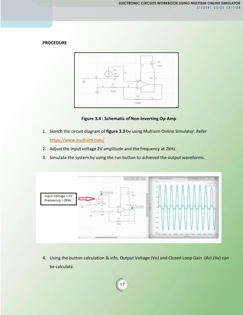
PROCEDURE
Figure 3.4 : Schematic of Non-Inverting Op-Amp
1. Sketch the circuit diagram of figure 3.3 by using Multisim Online Simulator. Refer
https://www.multisim.com/
2. Adjust the input voltage 2V amplitude and the frequency at 2kHz.
3. Simulate the system by using the run button to achieved the output waveforms.
4. Using the button calculation & info, Output Voltage (Vo) and Closed Loop Gain (Acl /Av) can
be calculate.
ELECTRONIC CIRCUITS WORKBOOK USING MULTISIM ONLINE SIMULATOR
S T U D E N T G U I D E E D I T I O N
18
OUTPUT
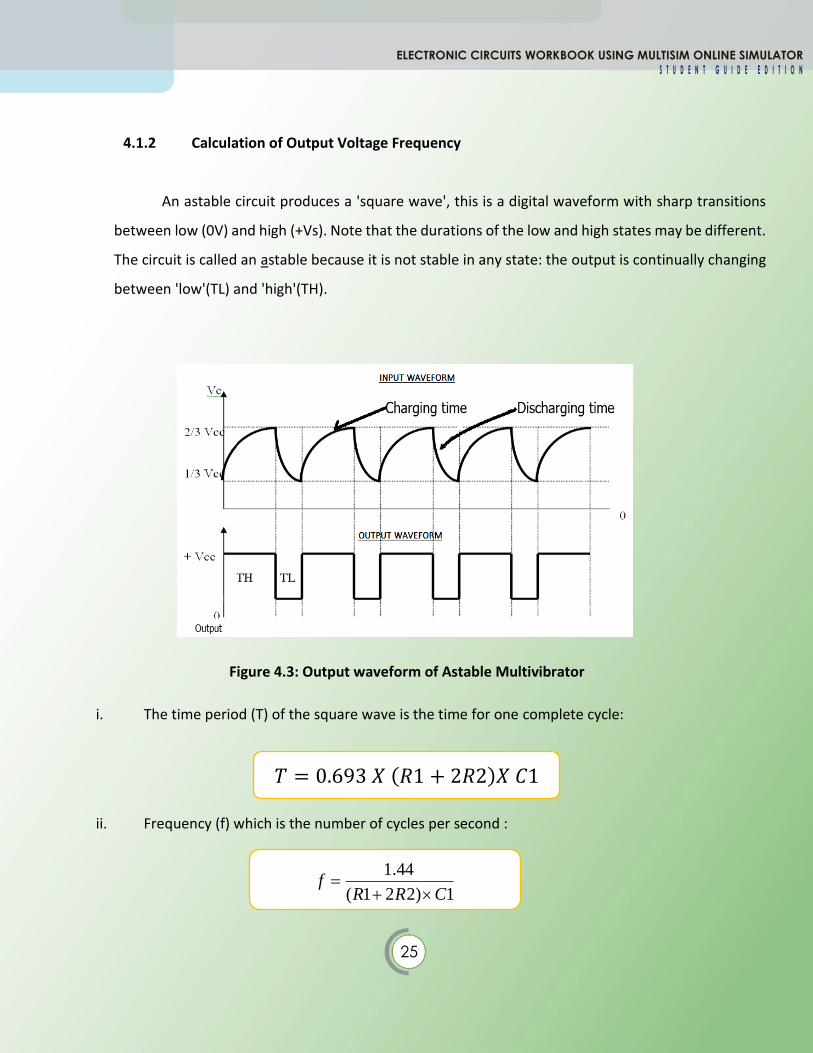
1. Input Waveform & Output Waveform
2. Vin = Vpp
ELECTRONIC CIRCUITS WORKBOOK USING MULTISIM ONLINE SIMULATOR
S T U D E N T G U I D E E D I T I O N

19
3. Vout
Calculation of Output Voltage, Vout
Vo = 1 + [𝑅𝑓
𝑅𝑖] 𝑉𝑖
Vo = 1 + [10𝑘
1𝑘] 2
Vo = 21 V
ELECTRONIC CIRCUITS WORKBOOK USING MULTISIM ONLINE SIMULATOR
S T U D E N T G U I D E E D I T I O N

20
Calculation of Gain, Acl
𝐴𝑐𝑙 = 𝑉𝑜
𝑉𝑖
𝐴𝑐𝑙 = 21.959 𝑉
1.9995 𝑉
𝑨𝒄𝒍 = 𝟏𝟎. 𝟗𝟖𝟐
4. Measure of T to calculate phase angle value
ELECTRONIC CIRCUITS WORKBOOK USING MULTISIM ONLINE SIMULATOR
S T U D E N T G U I D E E D I T I O N

21
Phase Angle, Ɵ
t = difference time between
input and output
T = time period
𝜽 = 𝒕
𝑻 𝑿 𝟑𝟔𝟎°
𝜽 = 𝟎
𝟓𝟎𝟓. 𝟓𝟗µ 𝑿 𝟑𝟔𝟎°
𝜽 = 𝟎° ( Vo and Vi is inphase )
ELECTRONIC CIRCUITS WORKBOOK USING MULTISIM ONLINE SIMULATOR
S T U D E N T G U I D E E D I T I O N

22
3.3 QUESTION
1.
a. Sketch the circuit diagram above by using Multisim Online Simulator.
b. Simulate to get the Output Voltage, Input Waveform and Output Waveform.
2.
a. Sketch the circuit diagram above by using Multisim Online Simulator.
b. Simulate to get the Output Voltage, Input Waveform and Output Waveform.
ELECTRONIC CIRCUITS WORKBOOK USING MULTISIM ONLINE SIMULATOR
S T U D E N T G U I D E E D I T I O N

23
ASTABLE MULTIVIBRATOR
4.1 INTRODUCTION
The 555 timer IC is an integrated circuit (chip) used in a variety of timer, pulse generation and oscillator
applications as show in figure 4.1.
(a) (b)
Figure 4.1: (a) Timer pinout and (b)Block diagram of TIMER 555 with pins
The 555 Timer Integrated Circuit (IC) can be designed either in its Monostable mode thus generating
a precision timer of a fixed time duration, or connect as Bistable mode to produce a flip-flop type
switching action. Other than that, it also can connect as Astable mode to produce a
stable Oscillator circuit for generating highly accurate free running waveforms whose output
frequency can be adjusted by means of an externally connected RC tank circuit consisting of just two
resistors and a capacitor.
In Astable Multivibrator, both output states are unstable state and output continuously changes
between the two states. The main application of this astable multivibrator is in the design of
relaxation oscillator.
UNIT 4

24
Figure 4.2: Astable using Timer 555 circuit
4.1.1 Operation of Astable using Timer 555
With the output high (+Vs) the capacitor C1 is charged by current flowing through R1 and R2.
The threshold and trigger inputs monitor the capacitor voltage and when it reaches 2/3Vs (threshold
voltage) the output becomes low and the discharge pin is connected to 0V. The capacitor now
discharges with current flowing through R2 into the discharge pin. When the voltage falls to1/3Vs
(trigger voltage) the output becomes high again and the discharge pin is disconnected, allowing the
capacitor to start charging again.
This cycle repeats continuously unless the reset input is connected to 0V which forces the output
low while reset is 0V. An astable can be used to provide the clock signal for circuits such as counters.
ELECTRONIC CIRCUITS WORKBOOK USING MULTISIM ONLINE SIMULATOR
S T U D E N T G U I D E E D I T I O N
25
4.1.2 Calculation of Output Voltage Frequency
An astable circuit produces a 'square wave', this is a digital waveform with sharp transitions
between low (0V) and high (+Vs). Note that the durations of the low and high states may be different.
The circuit is called an astable because it is not stable in any state: the output is continually changing
between 'low'(TL) and 'high'(TH).
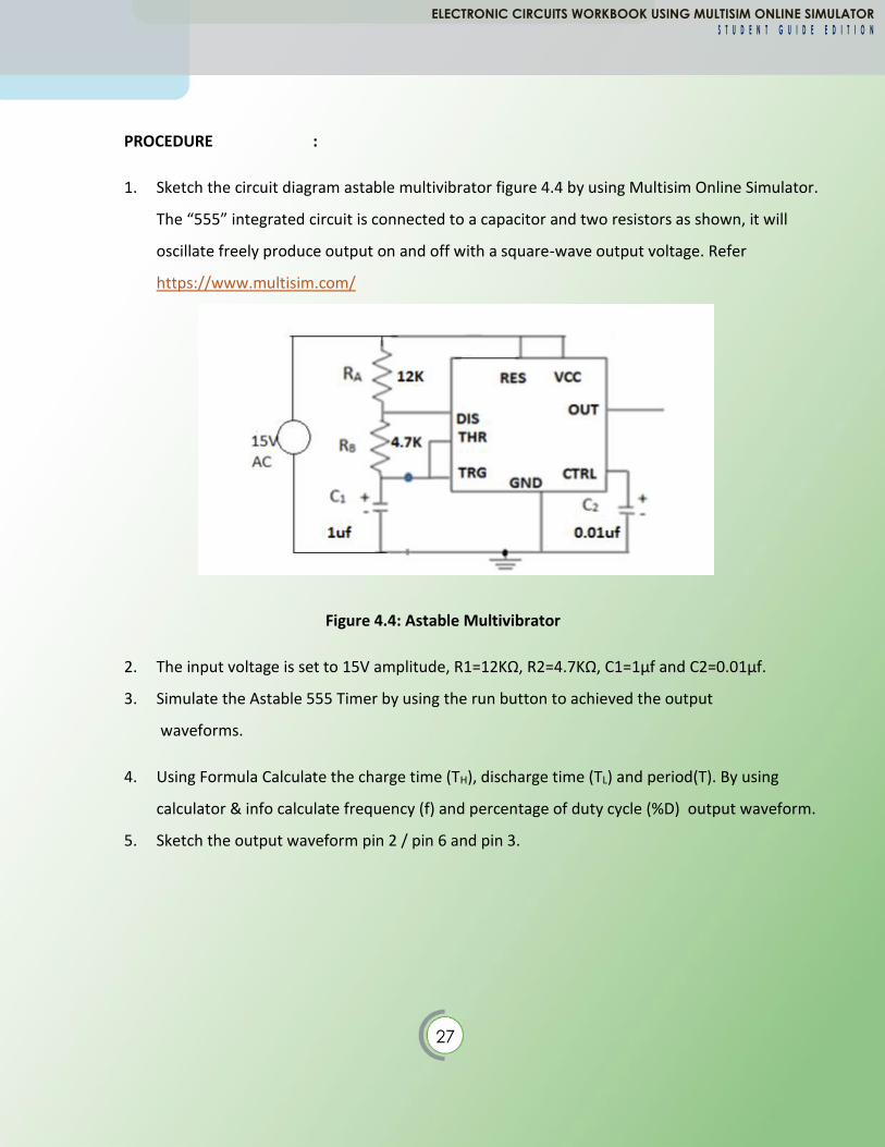
Figure 4.3: Output waveform of Astable Multivibrator
i. The time period (T) of the square wave is the time for one complete cycle:
𝑇 = 0.693 𝑋 (𝑅1 + 2𝑅2)𝑋 𝐶1
ii. Frequency (f) which is the number of cycles per second :
1)221(
44.1
CRRf
+=
ELECTRONIC CIRCUITS WORKBOOK USING MULTISIM ONLINE SIMULATOR
S T U D E N T G U I D E E D I T I O N

26
iii. The time period can be split into two parts:
iv. Mark time (output high):
v. Space time (output low):
vi. Percentage of duty cycle :
Hint: A 50% duty cycle means the high time is equal to the low time.
4.2 PRACTICAL OF ASTABLE MULTIVIBRATOR using TIMER (555) IC
OBJECTIVES
i. Able to construct of Astable 555 timer circuit
ii. Able to draw the waveform at the output (pin 3) and capacitor (pin 6).
iii. Able to measure the specification for Astable 555 Mode (frequency (f), duty cycle (D), Time
High (TH), Time Low (TL) and period (T)
TLTHT +=
1)21(693.0 CRRTH +=
12693.0 CRTL =
10021
%2
21 +
+=
RR
RRCycleDuty
ELECTRONIC CIRCUITS WORKBOOK USING MULTISIM ONLINE SIMULATOR
S T U D E N T G U I D E E D I T I O N
27
PROCEDURE :
1. Sketch the circuit diagram astable multivibrator figure 4.4 by using Multisim Online Simulator.
The “555” integrated circuit is connected to a capacitor and two resistors as shown, it will
oscillate freely produce output on and off with a square-wave output voltage. Refer
https://www.multisim.com/
Figure 4.4: Astable Multivibrator
2. The input voltage is set to 15V amplitude, R1=12KΩ, R2=4.7KΩ, C1=1µf and C2=0.01µf.
3. Simulate the Astable 555 Timer by using the run button to achieved the output
waveforms.
4. Using Formula Calculate the charge time (TH), discharge time (TL) and period(T). By using
calculator & info calculate frequency (f) and percentage of duty cycle (%D) output waveform.
5. Sketch the output waveform pin 2 / pin 6 and pin 3.
ELECTRONIC CIRCUITS WORKBOOK USING MULTISIM ONLINE SIMULATOR
S T U D E N T G U I D E E D I T I O N
28
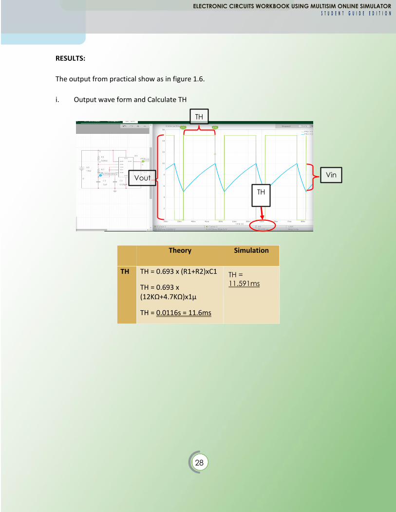
RESULTS:
The output from practical show as in figure 1.6.
i. Output wave form and Calculate TH
Theory Simulation
TH TH = 0.693 x (R1+R2)xC1
TH = 0.693 x (12KΩ+4.7KΩ)x1µ
TH = 0.0116s = 11.6ms
TH
Vin Vout
TH
TH =
11.591ms
ELECTRONIC CIRCUITS WORKBOOK USING MULTISIM ONLINE SIMULATOR
S T U D E N T G U I D E E D I T I O N
29
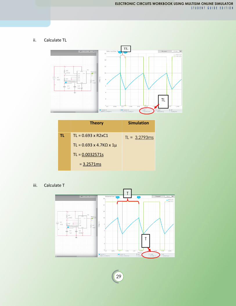
ii. Calculate TL
iii. Calculate T
Theory Simulation
TL TL = 0.693 x R2xC1
TL = 0.693 x 4.7KΩ x 1µ
TL = 0.0032571s
= 3.2571ms
TL
T
T
TL = 3.2793ms
ELECTRONIC CIRCUITS WORKBOOK USING MULTISIM ONLINE SIMULATOR
S T U D E N T G U I D E E D I T I O N

30
iv. Calculate Duty cycle.
4.3 QUESTION
1. The basis for this circuit’s timing as in figure 4.4, explain the function of resistor – capacitor(RC)
network:
2. Determine the TH, TL, T for the astable multivibrator in figure 4.4, if the value of R1 is varying
from 2KΩ, 10KΩ, 15KΩ and 56KΩ using multisim simulator.
3. Determine the TH, TL, T for the astable multivibrator in figure 4.4, if the value of R2 is varying
from 1KΩ, 3.9KΩ, 5.6KΩ and 10KΩ using multisim simulator.
4. Determine the TH, TL, T for the astable multivibrator in figure 4.4, if the value of C1 is varying
from 0.1µ, 0.2µ, 0.5µ and 10µ using multisim simulator.
Theory Simulation
T T = TH + TL
=(11.6+3.2571)ms
= 14.8471ms
%7810021400
16700%
100)7.42(12
)7.412(%
10021
%2
21
=
=
+
+=
+
+=
xDutyCycle
xKxK
KKDutyCycle
RR
RRCycleDuty
T =
14.857ms
ELECTRONIC CIRCUITS WORKBOOK USING MULTISIM ONLINE SIMULATOR
S T U D E N T G U I D E E D I T I O N
31
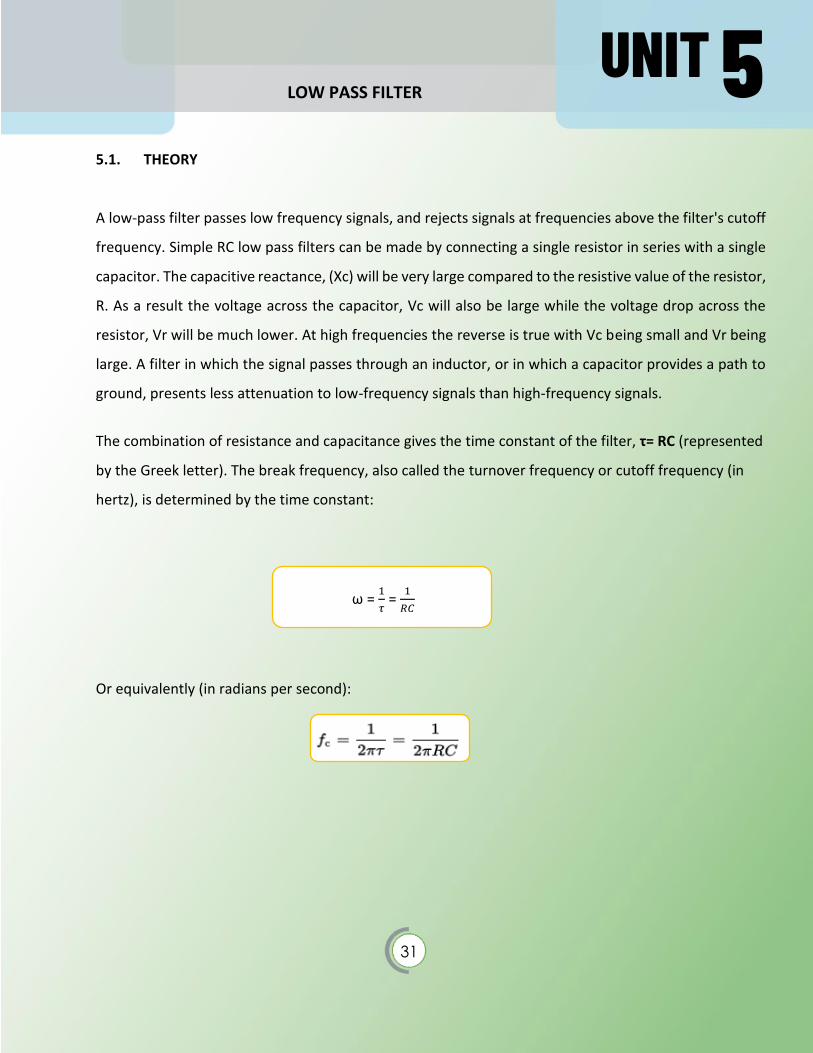
LOW PASS FILTER
5.1. THEORY
A low-pass filter passes low frequency signals, and rejects signals at frequencies above the filter's cutoff
frequency. Simple RC low pass filters can be made by connecting a single resistor in series with a single
capacitor. The capacitive reactance, (Xc) will be very large compared to the resistive value of the resistor,
R. As a result the voltage across the capacitor, Vc will also be large while the voltage drop across the
resistor, Vr will be much lower. At high frequencies the reverse is true with Vc being small and Vr being
large. A filter in which the signal passes through an inductor, or in which a capacitor provides a path to
ground, presents less attenuation to low-frequency signals than high-frequency signals.
The combination of resistance and capacitance gives the time constant of the filter, τ= RC (represented
by the Greek letter). The break frequency, also called the turnover frequency or cutoff frequency (in
hertz), is determined by the time constant:
ω = 1
𝜏 =
1
𝑅𝐶
Or equivalently (in radians per second):
UNIT 5

32
𝑓𝑐 =1
2𝜋𝑅𝐶
𝑓𝑐 =1
2𝜋𝑅𝐶
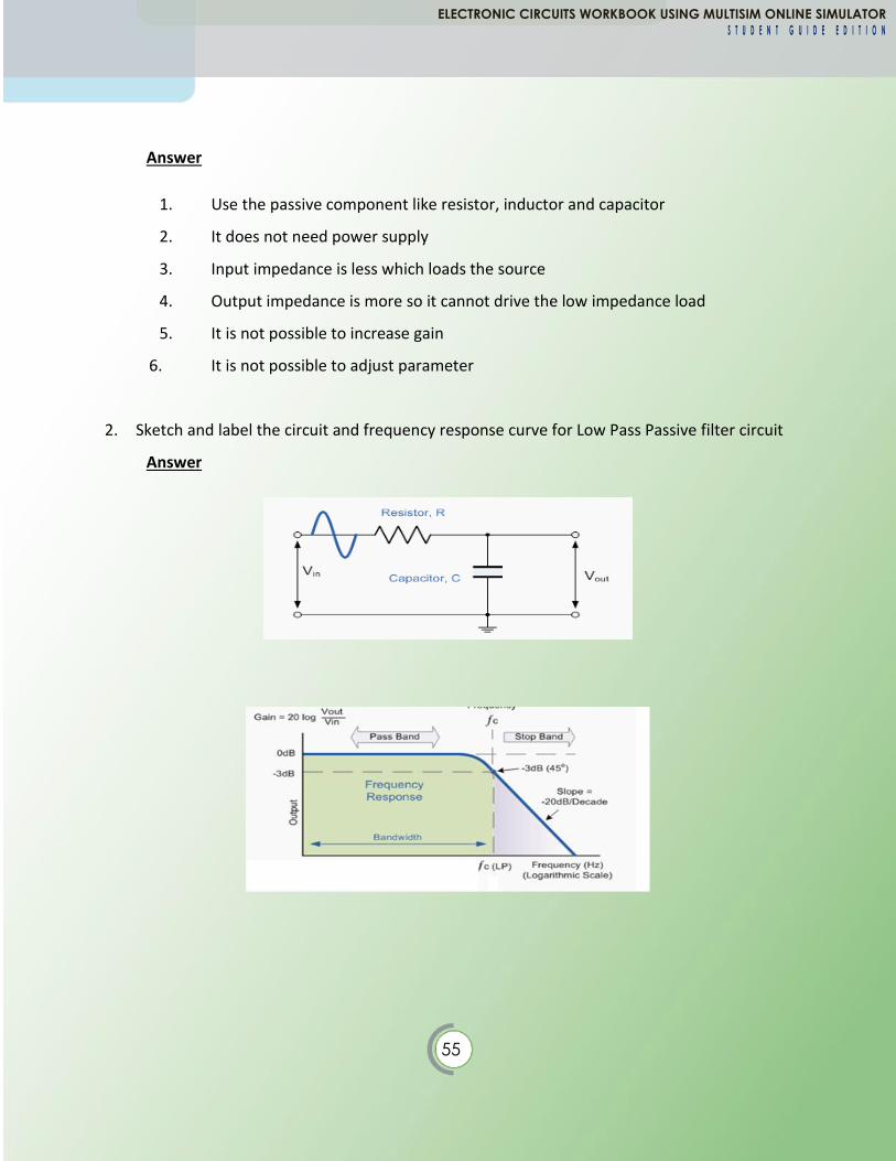
Figure 5.1 and 5.2 show the Low Pass filter circuit and Frequency response curve respectively.
Figure 5. 1 Low Pass filter circuit
Figure 5.2 : Frequency response curve for low pass filter
The cut-off frequency or - 3dB point, can be found using the Equation 1.
Cutoff Frequency,
Voltage gain is referred to the ratio of circuit output to input voltage as shown in Equation 2.
Vin
VoutAv =
…………………….. ( 1 )
…………………….. ( 2 )
ELECTRONIC CIRCUITS WORKBOOK USING MULTISIM ONLINE SIMULATOR
S T U D E N T G U I D E E D I T I O N
33
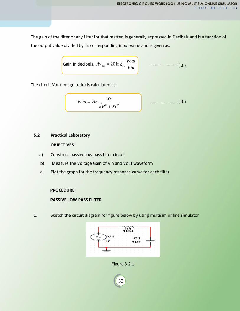
The gain of the filter or any filter for that matter, is generally expressed in Decibels and is a function of
the output value divided by its corresponding input value and is given as:
Gain in decibels, Vin
VoutAvdB 10log20=
The circuit Vout (magnitude) is calculated as:
22 XcR
XcVinVout
+=
5.2 Practical Laboratory
OBJECTIVES
a) Construct passive low pass filter circuit
b) Measure the Voltage Gain of Vin and Vout waveform
c) Plot the graph for the frequency response curve for each filter
PROCEDURE
PASSIVE LOW PASS FILTER
1. Sketch the circuit diagram for figure below by using multisim online simulator
Figure 3.2.1
…………………….. ( 3 )
…………………….. ( 4 )
ELECTRONIC CIRCUITS WORKBOOK USING MULTISIM ONLINE SIMULATOR
S T U D E N T G U I D E E D I T I O N

34
2. Simulate the system by using the run button to achieved the output waveforms.
3. Calculate Vout by using the given formula.
22 XcR
XcVinVout
+=
Where ; 𝑿𝒄 = 𝟏/𝟐𝝅𝑭𝑪 and 𝒛 = √𝒙𝒄𝟐 + 𝑹𝟐
Therefore; 𝒗𝟎 = 𝒗𝒊𝒏 (𝒙𝒄
𝒛)
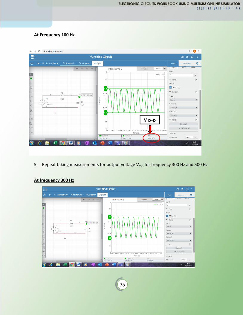
4. Set the input voltage Vin = 2Vp-p and frequency F = 100 Hz. Measure the input voltage
Vin and the output voltage Vout .
Output
1. Input and output waveform at Vin = 2Vp-p
2Vp-p Vin
Vo
o
Frequency Value
ELECTRONIC CIRCUITS WORKBOOK USING MULTISIM ONLINE SIMULATOR
S T U D E N T G U I D E E D I T I O N
35
At Frequency 100 Hz
5. Repeat taking measurements for output voltage Vout for frequency 300 Hz and 500 Hz
At frequency 300 Hz
V p-p
ELECTRONIC CIRCUITS WORKBOOK USING MULTISIM ONLINE SIMULATOR
S T U D E N T G U I D E E D I T I O N

36
At frequency 500 Hz
5.3 QUESTION
1. By using multisim online simulator, sketch the same circuit as in figure 3.2.1, measure the input
voltage Vin and the output voltage Vout with the frequency of 1KHz, 5KHz, 10KHz, 20KHz, 30KHz
and 50KHz. Then draw the a graph of Gain (Av) Vs Frequency
5.4 Exercises
1. List SIX (6) characteristics for passive filter circuit.
2. Sketch and label the circuit and frequency response curve for Low Pass Passive filter circuit
ELECTRONIC CIRCUITS WORKBOOK USING MULTISIM ONLINE SIMULATOR
S T U D E N T G U I D E E D I T I O N

37
DIGITAL TO ANALOG CONVERTER
6.1 THEORY
Digital to analog converter (DAC) was used to convert digital signals to analog signals. The
output signal from a computer connected to the DAC, where the DAC converts this signal is an analog
voltage or current. Example: Computer manufactures digital output signal range from 000000002 to
111111112, where the DAC converts the voltage range of 0 to 10V.
DAC Block Diagram
Binary Weighted Resistor DAC circuit was design by using several resistor values. The output voltage
of the DAC can be determined as follow:
Analog Output Digital Input
A
B
C
D
DAC 4-bit Vout
1s
2s
4s
8s
Figure 6.1: Block Diagram for DAC
UNIT 6

38
Figure 6.2: 4-Bit Binary Weighted Resistor DAC
The circuit in figure 6.2 above is a digital to analog converter circuit of resistors 4-bit binary weights.
The resistor values can be calculated using the weighting of the binary number.
6.2 Practical Laboratory
OBJECTIVES
i. Construct the circuits DAC type Resistive divider circuit
ii. Measure the Resistive divider circuit’s output.
PROCEDURES:
1. Draw circuit as in figure below by using multisim online simulator
ELECTRONIC CIRCUITS WORKBOOK USING MULTISIM ONLINE SIMULATOR
S T U D E N T G U I D E E D I T I O N
39
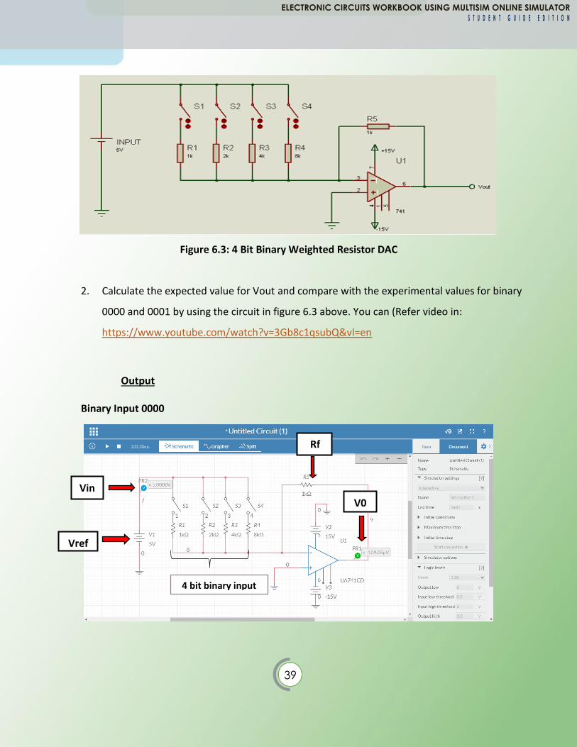
Figure 6.3: 4 Bit Binary Weighted Resistor DAC
2. Calculate the expected value for Vout and compare with the experimental values for binary
0000 and 0001 by using the circuit in figure 6.3 above. You can (Refer video in:
https://www.youtube.com/watch?v=3Gb8c1qsubQ&vl=en
Output
Binary Input 0000
Vin
V0
4 bit binary input
Rf
Vref
ELECTRONIC CIRCUITS WORKBOOK USING MULTISIM ONLINE SIMULATOR
S T U D E N T G U I D E E D I T I O N

40
Calculated Value
Vout = -Vref (4
f
3
f
2
f
R1
Rf
R
R
R
R
R
R+++ )
= - 5V (0 + 0 + 0 + 0)
= 0 V
Binary Input 0001
Calculated Value
Vout = -Vref (4
f
3
f
2
f
R1
Rf
R
R
R
R
R
R+++ )
= - 5V (0 + 0 + 0 + 1k/8k)
= 0.125 V
Close switch indicates binary 1
Open Switch indicates binary 0
ELECTRONIC CIRCUITS WORKBOOK USING MULTISIM ONLINE SIMULATOR
S T U D E N T G U I D E E D I T I O N

41
6.3 QUESTION
1. Repeat the procedure 1 and 2. Then calculate the calculated value of V0 by using the formulae
in figure 6.2. Compare the both values of calculated and measured values. Record all the
readings in the table 6.1
2. State the observation can be made from the value of Vout in the table.
Table 6.1
Decimal
Binary input
Analog output (Vout)
Analog output (Vout)
S1 S2 S3 S4 Calculated value Measured value
0 0 0 0 0
1 0 0 0 1
2 0 0 1 0
3 0 0 1 1
4 0 1 0 0
5 0 1 0 1
6 0 1 1 0
7 0 1 1 1
8 1 0 0 0
9 1 0 0 1
10 1 0 1 0
11 1 0 1 1
12 1 1 0 0
13 1 1 0 1
14 1 1 1 0
15 1 1 1 1
ELECTRONIC CIRCUITS WORKBOOK USING MULTISIM ONLINE SIMULATOR
S T U D E N T G U I D E E D I T I O N

42
Exercises
1.
Figure 6.4
The circuit in figure 6.4 is a digital to analog converter circuit of resistors 4-bit binary weights. By
using the weighting of the binary number, calculate the value for resistor R2, R3 and R4 and what
are the analogue output voltage will be generated if a digital input 0001 and 0110 were applied?
ELECTRONIC CIRCUITS WORKBOOK USING MULTISIM ONLINE SIMULATOR
S T U D E N T G U I D E E D I T I O N
43
Vo= Vin – (2 x 0.7V)
= (-6.0) - (-1.4)
= -4.6V
Vo= Vin – (2 x 0.7V)
= (-6.0) - (-1.4)
= -4.6V
ANSWERS
Unit 1
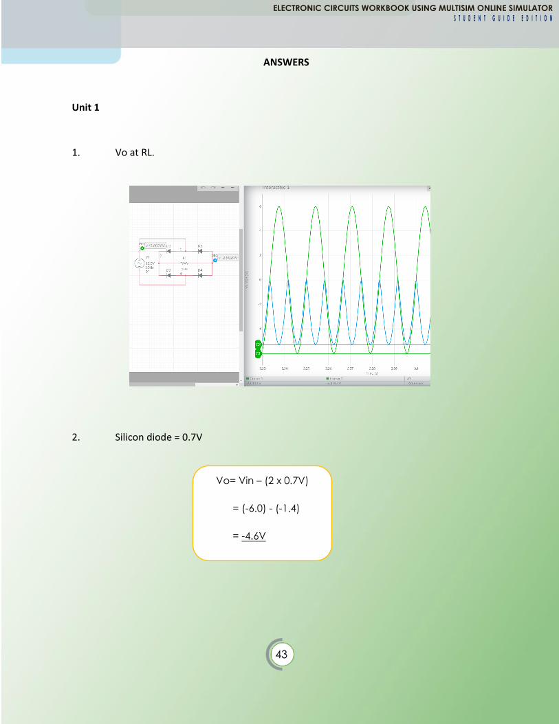
1. Vo at RL.
2. Silicon diode = 0.7V
ELECTRONIC CIRCUITS WORKBOOK USING MULTISIM ONLINE SIMULATOR
S T U D E N T G U I D E E D I T I O N
44
Vo = Vin – (2x0.3V)
= (3.0) - (0.712)
= 2.288V
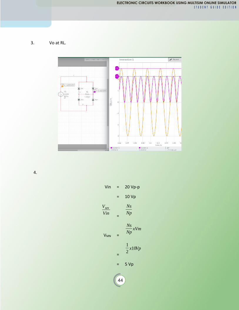
3. Vo at RL.
4.
Vin = 20 Vp-p
= 10 Vp
Vin
VMN
=
Ns
Np
VMN
=
Ns
NpxVm
=
1
210x Vp
= 5 Vp
ELECTRONIC CIRCUITS WORKBOOK USING MULTISIM ONLINE SIMULATOR
S T U D E N T G U I D E E D I T I O N

45
Unit 2
a.
then Vo = VMN
= 5 Vp
Output frequency signal
= 2 x frequency input signal
= 100 Hz
ELECTRONIC CIRCUITS WORKBOOK USING MULTISIM ONLINE SIMULATOR
S T U D E N T G U I D E E D I T I O N

46
b. Calculation of Output Frequency using formula :
𝐶𝑇 = 𝐶1𝑋𝐶2
𝐶1 + 𝐶2
𝐶𝑇 = 0.1µ𝑋0.1µ
0.1µ + 0.1µ= 50𝑛𝐹
𝑓𝑟 = 1
2𝜋√3𝑚 𝑥 50𝑛𝐹 = 12.995 kHz
Unit 3
1.a
ELECTRONIC CIRCUITS WORKBOOK USING MULTISIM ONLINE SIMULATOR
S T U D E N T G U I D E E D I T I O N
47
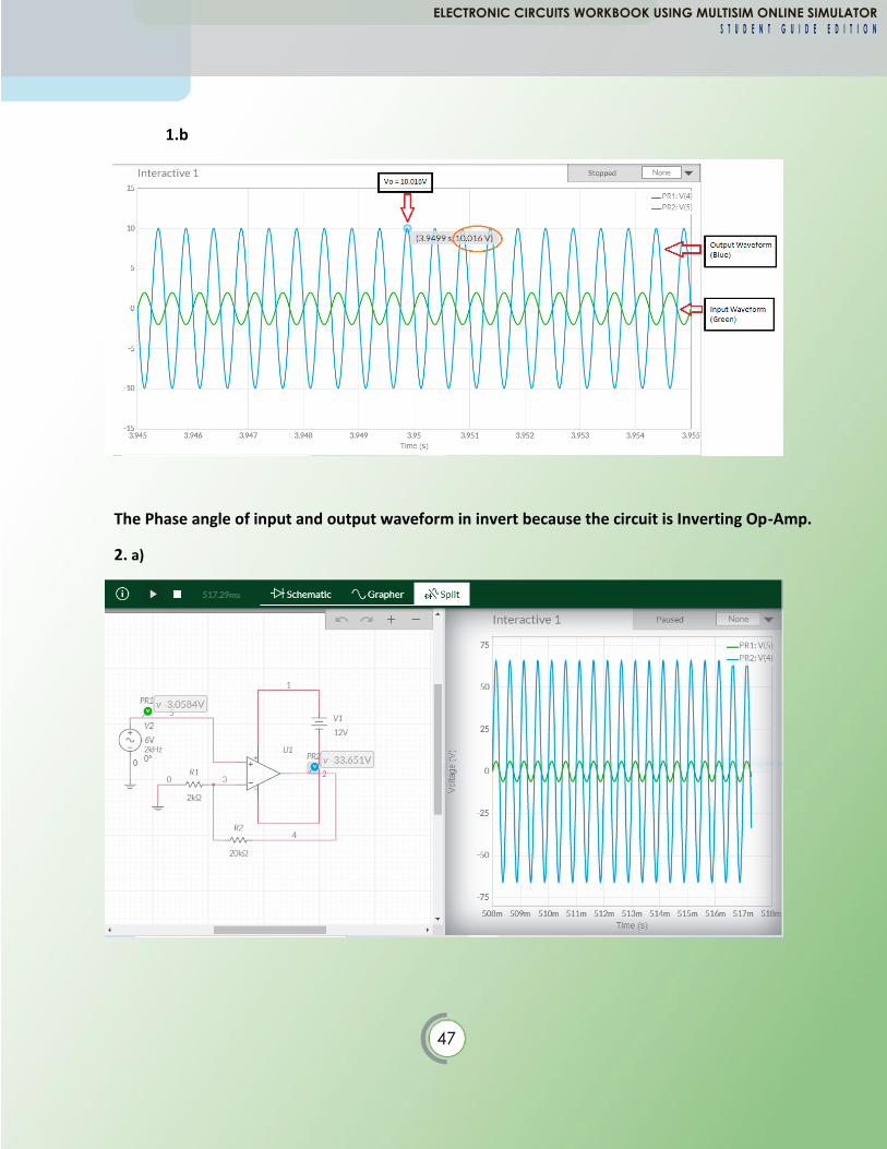
1.b
The Phase angle of input and output waveform in invert because the circuit is Inverting Op-Amp.
2. a)
ELECTRONIC CIRCUITS WORKBOOK USING MULTISIM ONLINE SIMULATOR
S T U D E N T G U I D E E D I T I O N
48
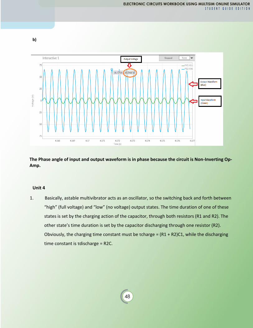
b)
The Phase angle of input and output waveform is in phase because the circuit is Non-Inverting Op-Amp.
Unit 4
1. Basically, astable multivibrator acts as an oscillator, so the switching back and forth between
“high” (full voltage) and “low” (no voltage) output states. The time duration of one of these
states is set by the charging action of the capacitor, through both resistors (R1 and R2). The
other state’s time duration is set by the capacitor discharging through one resistor (R2).
Obviously, the charging time constant must be τcharge = (R1 + R2)C1, while the discharging
time constant is τdischarge = R2C.
ELECTRONIC CIRCUITS WORKBOOK USING MULTISIM ONLINE SIMULATOR
S T U D E N T G U I D E E D I T I O N
49
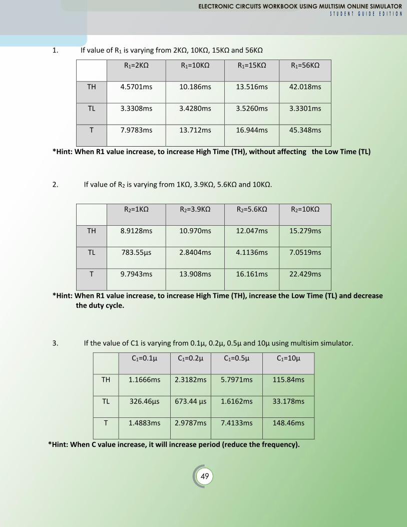
1. If value of R1 is varying from 2KΩ, 10KΩ, 15KΩ and 56KΩ
R1=2KΩ R1=10KΩ R1=15KΩ R1=56KΩ
TH 4.5701ms 10.186ms 13.516ms 42.018ms
TL 3.3308ms 3.4280ms 3.5260ms 3.3301ms
T 7.9783ms 13.712ms 16.944ms 45.348ms
*Hint: When R1 value increase, to increase High Time (TH), without affecting the Low Time (TL)
2. If value of R2 is varying from 1KΩ, 3.9KΩ, 5.6KΩ and 10KΩ.
R2=1KΩ R2=3.9KΩ R2=5.6KΩ R2=10KΩ
TH 8.9128ms 10.970ms 12.047ms 15.279ms
TL 783.55µs 2.8404ms 4.1136ms 7.0519ms
T 9.7943ms 13.908ms 16.161ms 22.429ms
*Hint: When R1 value increase, to increase High Time (TH), increase the Low Time (TL) and decrease the duty cycle.
3. If the value of C1 is varying from 0.1µ, 0.2µ, 0.5µ and 10µ using multisim simulator.
C1=0.1µ C1=0.2µ C1=0.5µ C1=10µ
TH 1.1666ms 2.3182ms 5.7971ms 115.84ms
TL 326.46µs 673.44 µs 1.6162ms 33.178ms
T 1.4883ms 2.9787ms 7.4133ms 148.46ms
*Hint: When C value increase, it will increase period (reduce the frequency).
ELECTRONIC CIRCUITS WORKBOOK USING MULTISIM ONLINE SIMULATOR
S T U D E N T G U I D E E D I T I O N
50
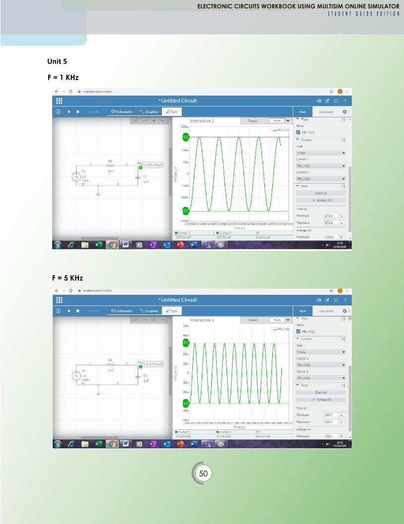
Unit 5
F = 1 KHz
F = 5 KHz
ELECTRONIC CIRCUITS WORKBOOK USING MULTISIM ONLINE SIMULATOR
S T U D E N T G U I D E E D I T I O N

51
F = 10 KHz
F = 20 KHz
ELECTRONIC CIRCUITS WORKBOOK USING MULTISIM ONLINE SIMULATOR
S T U D E N T G U I D E E D I T I O N

52
F = 30 KHz
F = 50 KHz
ELECTRONIC CIRCUITS WORKBOOK USING MULTISIM ONLINE SIMULATOR
S T U D E N T G U I D E E D I T I O N

53
F = 100 KHz
Freq(Hz) Av(dB)
100 -1.455
300 -6.564
500 -10.484
1000 -16.082
5000 -29.87
10000 -35.918
20000 -42.025
30000 -45.528
50000 -49.908
100000 -55.956
ELECTRONIC CIRCUITS WORKBOOK USING MULTISIM ONLINE SIMULATOR
S T U D E N T G U I D E E D I T I O N

54
Graph of Gain (Av) VS Frequency
Graph of Gain (Av) VS Frequency
3.4 Exercises
1. List SIX (6) characteristics for passive filter circuit.
-60
-50
-40
-30
-20
-10
0
Av(dB)
Av(dB)
ELECTRONIC CIRCUITS WORKBOOK USING MULTISIM ONLINE SIMULATOR
S T U D E N T G U I D E E D I T I O N
55
Answer
1. Use the passive component like resistor, inductor and capacitor
2. It does not need power supply
3. Input impedance is less which loads the source
4. Output impedance is more so it cannot drive the low impedance load
5. It is not possible to increase gain
6. It is not possible to adjust parameter
2. Sketch and label the circuit and frequency response curve for Low Pass Passive filter circuit
Answer
ELECTRONIC CIRCUITS WORKBOOK USING MULTISIM ONLINE SIMULATOR
S T U D E N T G U I D E E D I T I O N

56
Unit 6
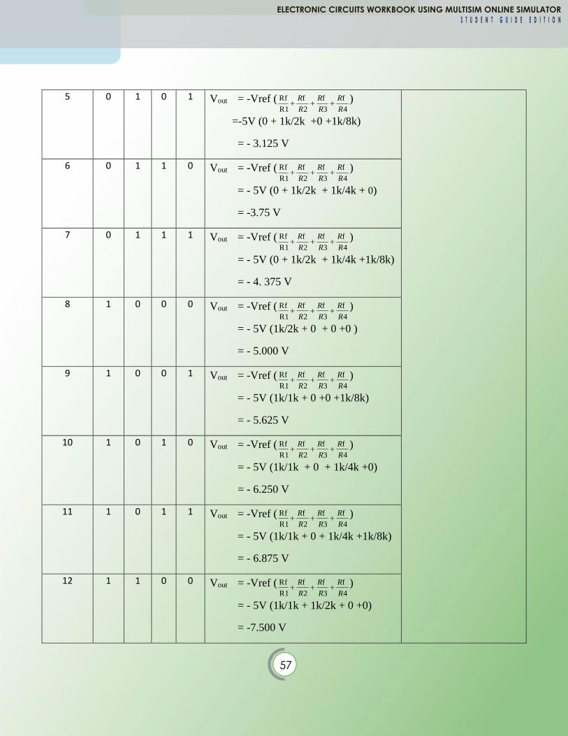
RESULT/ANALYSIS:
1.
Decimal
Binary input
Analog output (Vout)
Analog output (Vout)
S1 S2 S3 S4 Calculated value Measured value
0 0 0 0 0 Vout = -Vref (4
f
3
f
2
f
R1
Rf
R
R
R
R
R
R+++ )
= - 5V (0 + 0 + 0 + 0)
= 0 V
Vo from the experiment
(suppose the value will
be same as calculated
value or with minimum
error)
1 0 0 0 1 Vout = -Vref (4
f
3
f
2
f
R1
Rf
R
R
R
R
R
R+++ )
= - 5V (0 + 0 + 0 + 1k/8k)
= - 0.625 V
2 0 0 1 0 Vout = -Vref (4
f
3
f
2
f
R1
Rf
R
R
R
R
R
R+++ )
= - 5V (0 + 0 + 1k/4k + 0)
= - 1. 25 V
3 0 0 1 1 Vout = -Vref (4
f
3
f
2
f
R1
Rf
R
R
R
R
R
R+++ )
= -5V (0 + 0 + 1k/4k +1k/8k)
= - 1. 875 V
4 0 1 0 0 Vout = -Vref (4
f
3
f
2
f
R1
Rf
R
R
R
R
R
R+++ )
= - 5V (0 +1k/2k + 0+ 0)
= - 2.5 V
ELECTRONIC CIRCUITS WORKBOOK USING MULTISIM ONLINE SIMULATOR
S T U D E N T G U I D E E D I T I O N
57
5 0 1 0 1 Vout = -Vref (4
f
3
f
2
f
R1
Rf
R
R
R
R
R
R+++ )
=-5V (0 + 1k/2k +0 +1k/8k)
= - 3.125 V
6 0 1 1 0 Vout = -Vref (4
f
3
f
2
f
R1
Rf
R
R
R
R
R
R+++ )
= - 5V (0 + 1k/2k + 1k/4k + 0)
= -3.75 V
7 0 1 1 1 Vout = -Vref (4
f
3
f
2
f
R1
Rf
R
R
R
R
R
R+++ )
= - 5V (0 + 1k/2k + 1k/4k +1k/8k)
= - 4. 375 V
8 1 0 0 0 Vout = -Vref (4
f
3
f
2
f
R1
Rf
R
R
R
R
R
R+++ )
= - 5V (1k/2k + 0 + 0 +0 )
= - 5.000 V
9 1 0 0 1 Vout = -Vref (4
f
3
f
2
f
R1
Rf
R
R
R
R
R
R+++ )
= - 5V (1k/1k + 0 +0 +1k/8k)
= - 5.625 V
10 1 0 1 0 Vout = -Vref (4
f
3
f
2
f
R1
Rf
R
R
R
R
R
R+++ )
= - 5V (1k/1k + 0 + 1k/4k +0)
= - 6.250 V
11 1 0 1 1 Vout = -Vref (4
f
3
f
2
f
R1
Rf
R
R
R
R
R
R+++ )
= - 5V (1k/1k + 0 + 1k/4k +1k/8k)
= - 6.875 V
12 1 1 0 0 Vout = -Vref (4
f
3
f
2
f
R1
Rf
R
R
R
R
R
R+++ )
= - 5V (1k/1k + 1k/2k + 0 +0)
= -7.500 V
ELECTRONIC CIRCUITS WORKBOOK USING MULTISIM ONLINE SIMULATOR
S T U D E N T G U I D E E D I T I O N

58
2. From the table, we can say that the value for every step size increasing by 0.625 (starting from
0000 until binary 1111)
Exercises
1. Referring to figure 6.4, the highest value resistor (R1= 150KΩ) is a digital input resistor, then the
values of the other resistor is;
R2 = 11
1
2
150K
2
R= = 75k
13 1 1 0 1 Vout = -Vref (4
f
3
f
2
f
R1
Rf
R
R
R
R
R
R+++ )
= - 5V (1k/1k + 1k/2k + 0 +1k/8k)
= - 8.125 V
14 1 1 1 0 Vout = -Vref (4
f
3
f
2
f
R1
Rf
R
R
R
R
R
R+++ )
= - 5V (1k/1k + 1k/2k + 1k/4k +0)
= - 8.750 V
15 1 1 1 1 Vout = -Vref (4
f
3
f
2
f
R1
Rf
R
R
R
R
R
R+++ )
= - 5V(1k/1k+1k/2k+1k/4k+1k/8k)
= -9.375 V
3 1
4
2 2 1
3
18.75kΩ 8
150K
2
R R
, 37.5k 4
150K
2
150K
2
R R
= = =
= = = =
ELECTRONIC CIRCUITS WORKBOOK USING MULTISIM ONLINE SIMULATOR
S T U D E N T G U I D E E D I T I O N
59
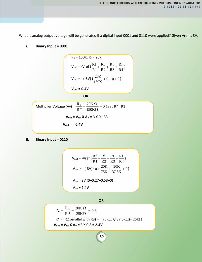
What is analog output voltage will be generated if a digital input 0001 and 0110 were applied? Given Vref is 3V.
i. Binary Input = 0001
R1 = 150K, RF = 20K
Vout = -Vref (R4
Rf
R3
Rf
R2
Rf
R1
Rf+++ )
Vout = - (-3V) ( 00 0150K
20K+++ )
Vout = 0.4V
OR
Multiplier Voltage (AV) = 0.133150K
20K
*R
R F =
= , R*= R1
Vout = Vref X AV = 3 X 0.133
Vout = 0.4V
ii. Binary Input = 0110
Vout = -Vref (R4
Rf
R3
Rf
R2
Rf
R1
Rf+++ )
Vout = - (-3V) ( 037.5K
20K
75K
20K0 +++ )
Vout= 3V (0+0.27+0.53+0)
Vout= 2.4V
OR
AV = 0.825K
20K
*R
R F =
=
R* = (R2 parallel with R3) = (75K // 37.5K)= 25K
Vout = Vref X AV = 3 X 0.8 = 2.4V
ELECTRONIC CIRCUITS WORKBOOK USING MULTISIM ONLINE SIMULATOR
S T U D E N T G U I D E E D I T I O N

60
REFERENCES
DEE30043 ELECTRONICS CIRCUIT LABSHEET
Electronic Devices and Circuit Theory, Eight Edition, Robert L.Boylested, Louis Nashelsky, Prentice
Hall, 2002
https://www.electronics-tutorials.ws/diode/diode_6.html
https://www.electrical4u.com/bridge-rectifiers/
https://www.electrical4u.com/full-wave-rectifiers/
https://www.google.com/search?q=rectifier+diode&tbm=isch&hl=ms&chips=q:rectifier+diode,online
chips:bridge+rectifier+circuit+diagram:i798ByxtWlo%3D,online_chips:output+voltage:EJjByKUJqT4%3
D&rlz=1C1GCEU_enMY865MY865&sa=X&ved=2ahUKEwiG74yJpufyAhVUcSsKHUB5ABwQ4lYoAnoECA
EQGA&biw=979&bih=685#imgrc=gnLjrZCBenKKLM
https://www.ablic.com/en/semicon/products/analog/opamp/intro/
https://www.brainkart.com/media/article/articleunp3kaabpicture11.jpg
https://www.brainkart.com/article/Circuit-symbol-and-Pin-out-configuration-of-an-OP-
AMP_3003/
https://www.multisim.com/
https://www.youtube.com/watch?v=iJYm_BGqa1A
https://www.allaboutcircuits.com/tools/555-timer-astable-circuit/
https://www.allaboutcircuits.com/worksheets/timer-circuits/
https://www.allaboutcircuits.com/textbook/experiments/chpt-6/555-audio-oscillator/
https://www.electronics-tutorials.ws/waveforms/555_oscillator.html
https://www.electronicshub.org/astable-multivibrator-using-555-
timer/#Astable_Multivibrator_Mode_of_555_Timer_IC
ELECTRONIC CIRCUITS WORKBOOK USING MULTISIM ONLINE SIMULATOR
S T U D E N T G U I D E E D I T I O N

61
https://www.electronics-tutorials.ws/filter/filter_2.html
https://www.youtube.com/watch?v=lagfhNjMuQM
https://nanohub.org/resources/14905/download/LOW_PASS_FILTERS.pdf
https://en.wikipedia.org/wiki/Low-pass_filter#/media/File:Butterworth_response.svg
ELECTRONIC CIRCUITS WORKBOOK USING MULTISIM ONLINE SIMULATOR
S T U D E N T G U I D E E D I T I O N


