

ÉC OLE PO LY TEC H NIQ U EFÉ DÉRALE D E LAUSAN NE
EPFL CENTER OF MICRONANOTECHNOLOGY
1

ÉC OLE PO LY TEC H NIQ U EFÉ DÉRALE D E LAUSAN NE
EPFL CENTER OF MICRONANOTECHNOLOGY
2
Des technologies de microfabricationde pointe accessibles aux PME
Cyrille Hibert, EPFL

ÉC OLE PO LY TEC H NIQ U EFÉ DÉRALE D E LAUSAN NE
CMI MISSION
Support Education
Support Research
Provide Access to NanoFabrication Processes
3
ÉC OLE PO LY TEC H NIQ U EFÉ DÉRALE D E LAUSAN NE
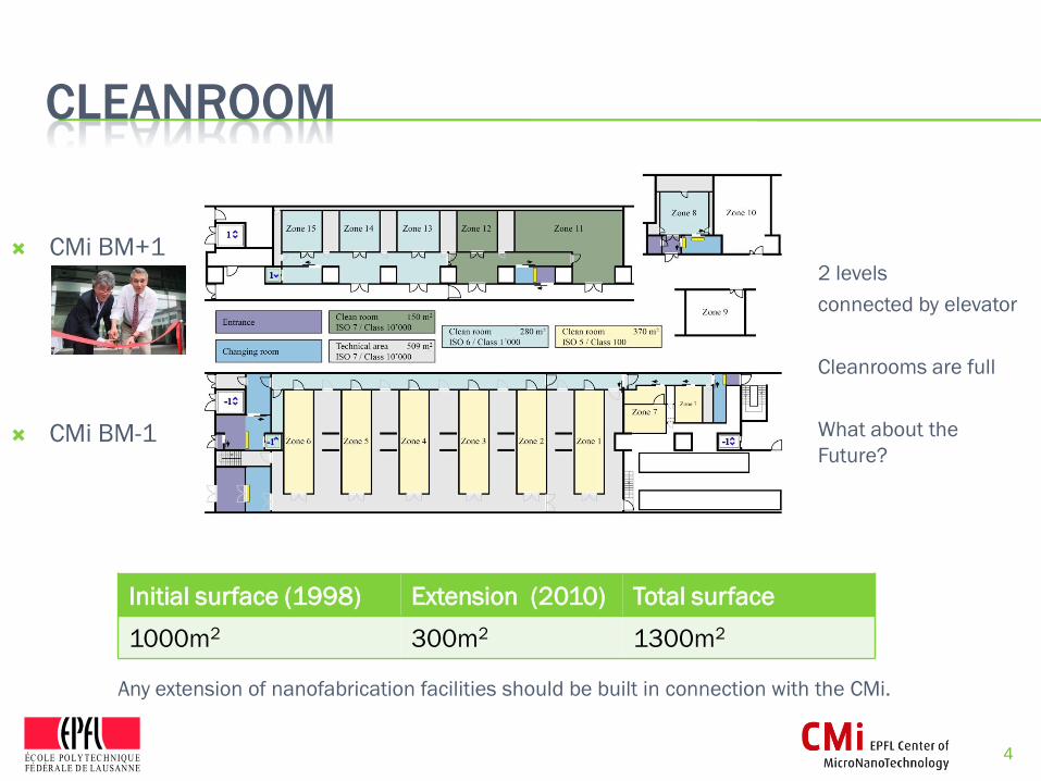
CLEANROOM
4
Initial surface (1998) Extension (2010) Total surface
1000m2 300m2 1300m2
CMi BM-1
CMi BM+12 levels
connected by elevator
Cleanrooms are full
What about the
Future?
Any extension of nanofabrication facilities should be built in connection with the CMi.

ÉC OLE PO LY TEC H NIQ U EFÉ DÉRALE D E LAUSAN NE
CMI CLEANROOM
5
ACTUAL VALUES (2/3 of
maximum capacity)
FRESH AIR
60’000 m3/h
filter efficiency: 99.97% for
particles size: 0.1-0.3 µm
EXHAUST
36 ’000 m3/h
FFU
ISO 5 : 189 units
ISO 6 and 7 : 46 units
0.7 m2 active area
total: 189’000 m3/h
filter efficiency : 99.999% for
particles size 0.1-0.3 µm
Description of the CleanroomAir filtration and circulation in class 100

ÉC OLE PO LY TEC H NIQ U EFÉ DÉRALE D E LAUSAN NE
CMI CLEANROOM
6

ÉC OLE PO LY TEC H NIQ U EFÉ DÉRALE D E LAUSAN NE
CMI CLEANROOM
7
Bay and Chase Cleanroom Arrangement

ÉC OLE PO LY TEC H NIQ U EFÉ DÉRALE D E LAUSAN NE
CMI CLEANROOM
8
Electricity consumption CMi (2014) : 2’519’878 kWh (CHF 348’191.-)
Nitrogen consumption (2014) : 356’646 m3 of gas (CHF 65’706.-)
(1lt of liquid = 700lt of gas)
Heating energy BM (2014) 1’571’083 kWh (CHF 146’925.-)
Water consumption BM (2014) Reverse Osmosis : 16’936m3 (CHF 62’726.-)
Cooling : 595’025m3 (CHF 141’043.-)
Total Energy & Fluids : CHF 764’591.-

ÉC OLE PO LY TEC H NIQ U EFÉ DÉRALE D E LAUSAN NE
CMI CAPITAL INVESTMENT
Processing Equipment
Cleanroom Infrastructures
Total 50MCHF
9
Scientific Equipment Level -1 28 MCHF
Scientific Equipment Level +1 3 MCHF
Total 31 MCHF
Cleanroom Infrastructures Level -1 12 MCHF
Cleanroom Infrastructures Level +1 7 MCHF
Total 19 MCHF

ÉC OLE PO LY TEC H NIQ U EFÉ DÉRALE D E LAUSAN NE
THE STAFF
10
19.2 FTE staff members
+ Student assistants
+ Apprentices

ÉC OLE PO LY TEC H NIQ U EFÉ DÉRALE D E LAUSAN NE
USERS IN 2016
11
EPFL Engineering Sc. Basic Sc. Life Sc. Ext. Ac. CompaniesCMi STI-IMT-LMIS2 SB-CMNT-GE SV-GHI-UPKIN EXT-CERN EXT-Aleva EXT-SilMach
STI-IBI-BIOS STI-IMT-LMIS4 SB-IPHYS-GCMP SV-IBI-LDCS EXT-CSEM-T1 EXT-Asulab EXT-SwissTo12
STI-IBI-CLSE STI-IMT-LMTS SB-IPHYS-LASPE SV-IBI-LLCB EXT-CSEM-T3 EXT-Bruker EXT-Synova
STI-IBI-LBEN STI-IMT-LO SB-IPHYS-LOEQ SV-IBI-LMRP EXT-CSEM-Mut. EXT-Colibrys EXT-TESCAN
STI-IBI-LBNC STI-IMT-LOB SB-IPHYS-LPMC SV-IBI-UPDEPLA EXT-EMPA EXT-Efficonseil EXT-Tronics
STI-IBI-LBNI STI-IMT-LPMAT SB-IPHYS-LPMV SV-IBI-UPLUT EXT-ETHZ EXT-EXALOS EXT-ValFleurier
STI-IBI-LHTC STI-IMT-LSBI SB-IPHYS-LPN SV-IBI-UPNAE EXT-HEIG-VD EXT-Hamamatsu
STI-IBI-LNE STI-IMT-NAM SB-IPHYS-LPQM1 SV-ISREC-CDTSO EXT-HESGE EXT-Hightec
STI-IEL-GR-SCI STI-IMT-NE-PV-LAB SB-IPHYS-LUMES SV-PTBIOEM EXT-HESNE EXT-Intel
STI-IEL-LANES STI-IMT-OPT SB-ISIC-LCPM EXT-Bucharest EXT-Karmic
STI-IEL-LEMA STI-IMT-PV-LAB SB-ISIC-LEPA EXT-Inst-Pasteur EXT-LémanMicro
STI-IEL-LSI2 STI-IMX-FIMAP SB-ISIC-LND IC-IINFCOM-LSI1 EXT-Belo-Horiz. EXT-LESS_SA
STI-IEL-LSM STI-IMX-LC SB-ISIC-LPI EXT-UNIBE-Phys. EXT-LSPR
STI-IEL-NANOLAB STI-IMX-LMGN SB-ISIC-LSCI ENAC-IIC-LESO-PB EXT-UniFribourg EXT-Lunaphore
STI-IEL-PHOSL STI-IMX-LMM SB-ISIC-LSPM EXT-UNIGE-GAP EXT-Mackinac
STI-IEL-POWERLAB STI-IMX-LMOM SB-ISIC-LSU EXT-UNIGE-Sugi. EXT-Meister-Abrasive
STI-IGM-LRESE STI-IMX-LMSC SB-SPC-PP EXT-UNIL EXT-Morphotonix
STI-IGM-MICROBS STI-IMX-LP EXT-Wyss_Cent EXT-Nanoworld
STI-IMT-ESPLAB STI-IMX-LTP EXT-Novagan
STI-IMT-GR-LVT STI-IMX-SMAL EXT-Piemacs
STI-IMT-GR-QUA STI-IMX-SUNMIL EXT-Qwane
STI-IMT-LAI STI-SCI-CD EXT-Rolex
STI-IMT-LAPD STI-SCI-PM EXT-Samtec
STI-IMT-LMIS1 EXT-Sigatec
342 (47) 65 (17) 37 (11) 40 (18) 46 (30)
Total: 530 users (+10%) operating the CMi tools
Total: 123 labs or companies (+23%)
ÉC OLE PO LY TEC H NIQ U EFÉ DÉRALE D E LAUSAN NE
USERS IN 2016
12
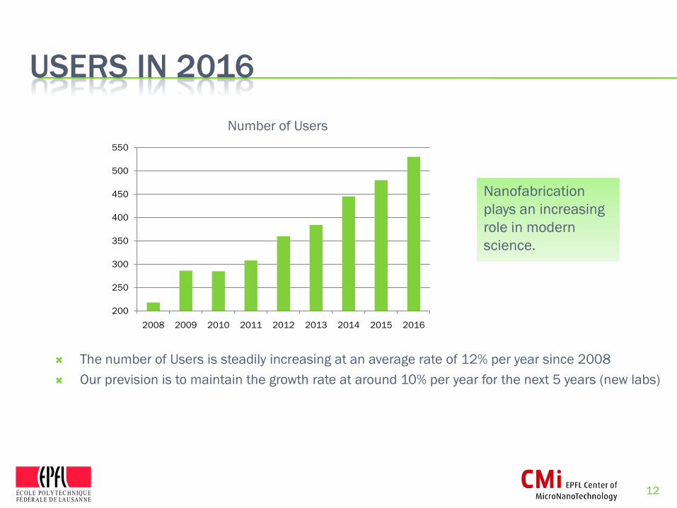
The number of Users is steadily increasing at an average rate of 12% per year since 2008
Our prevision is to maintain the growth rate at around 10% per year for the next 5 years (new labs)
Number of Users
Nanofabrication
plays an increasing
role in modern
science.
200
250
300
350
400
450
500
550
2008 2009 2010 2011 2012 2013 2014 2015 2016

ÉC OLE PO LY TEC H NIQ U EFÉ DÉRALE D E LAUSAN NE
ANNUAL REVIEW MEETING
18th edition on May 2nd 2017
More than 488 participants
203 abstracts
13
Global companies
Local industry
Startups
Many Suppliers
Government Agencies
Researchers
Faculties
Other academic cleanrooms
-> Traveling from over 15 countries -> Networking & Connecting the dots

ÉC OLE PO LY TEC H NIQ U EFÉ DÉRALE D E LAUSAN NE
BECOME A MEMBER
14
1. Cleanroom Introduction Course (0.5 day)
Formal presentation of CMi facilities and CMi rules
Cleanroom visit
Email from CMi secretary (username, password, process flow template)
2. Process Flow
You send a process flow or a draft to [email protected]
Process flow review with a technical committee (with CMi engineers, advices on design and process, training plan on equipment)
3. Start working in the cleanroom
Trainings
Rights to book equipment
Work on your own following a process flow
(reservation, login, processing, logout…)
Procedure to access the cleanroom

ÉC OLE PO LY TEC H NIQ U EFÉ DÉRALE D E LAUSAN NE
BECOME A MEMBER
15
CMi Website
CMi website tour :
http://cmi.epfl.ch/
Equipment user manual
Equipment reservation
Material ordering…

ÉC OLE PO LY TEC H NIQ U EFÉ DÉRALE D E LAUSAN NE
FEES
16
Since October 1st 2016
No more cap per user and per month (previously CHF 1600.- / academic user / month)
No more free access (for master & semester projects)
18 categories of tools (instead of uniform price per tool) :
with fees ranging from 20.- to 126.- CHF/h for internal EPFL Users
with fees ranging from 21.- to 171.- CHF/h for External Academic Users
with fees ranging from 30.8 to 323.40 CHF/h for Industrial Users
In general new system cheaper for occasional users and more expensive for heavy users
Globally no budget change for the operations of the CMi

CMi cleanroom technologies tour
CMi-EPFL 17

CMi-EPFL
CMi cleanroom technologies tour
• Lithography• Ebeam lithography• Photo lithography
• Thin Films• Etching• Misc. Processes• Metrology• Some examples
Courtesy of Silmach SA (Besançon)
18

CMi-EPFL
Ebeam Lithography
Key Features:
• 100keV Thermal Field Emission Gun• High Resolution Gaussian Beam System • 50MHz Intelligent Pattern Generator• 1.25nm minimum pixel size • Robust Direct Write Mark Detection &
Alignment Software • 2 position load lock for batch processing of
multiple substrates• Holders for 50mm, 100mm, 150mm wafers
and smaller piece parts • Housed in a custom cleanroom which
maintains a temperature of 21°C ± 0.1°C
19
CMi-EPFL
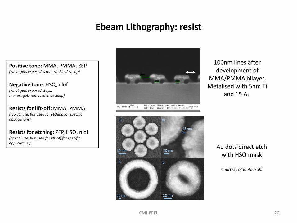
Ebeam Lithography: resist
100nm lines after development of
MMA/PMMA bilayer.Metalised with 5nm Ti
and 15 Au
Au dots direct etchwith HSQ mask
Courtesy of B. Abasahl
Positive tone: MMA, PMMA, ZEP(what gets exposed is removed in develop)
Negative tone: HSQ, nlof(what gets exposed stays, the rest gets removed in develop)
Resists for lift-off: MMA, PMMA(typical use, but used for etching for specificapplications)
Resists for etching: ZEP, HSQ, nlof(typical use, but used for lift-off for specificapplications)
20

CMi-EPFL
Photo Lithography: coating / development
• Automatic coating & development tools:
EVG150, Ritetrack 88, ACS200
• Manual coaters:
Sawatec LSM 200/250,
SSE SB20, Karl Süss RC-8
• Developer station:
Karl Süss DV10
• HMDS priming, Dehydration
EVG 150 coater & developer
RT 88 coater & developer
21

CMi-EPFL
Photo Lithography: exposure
• 2 Broadband mask-aligners
Karl Süss MA/BA6 & MA150
• I-line mask-aligner (Su8 soft lithography):
Karl Süss MJB4
• 2 Direct LASER lithography
Heidelbergh VPG200 & DWL200
Heidelberg VPG200 Laser writer
MJB4 mask-aligner
MA/BA6 mask-aligner
Write Mode 0 I II III IV
Minimum structure size [µm] 0.6 0.75 1 2 4
Write time for 100x100mm² [min] 210 38 12 4 2
22

CMi-EPFL
Photo Lithography: thin PR
• Negative (liftoff):
AZ nLof2020
• Thin positive resists (wet etch & high resolution):
AZ1512, AZECI3007
• Sacrificial (double-layer liftoff):
LOR 5A
nLof 2020 with negative sidewalls profile
AZ ECI 1:1 um sharp lines
AZ1512/LOR double-layer
23

CMi-EPFL
Photo Lithography: thick PR
Thick positive resists (dry etching & galvano):
AZ9221, AZ9260
AZECI 3027
Thick negative Su8 resist:
Gersteltec GM series
MCC 3000 series
200µm –thick Su8 with high aspect ratio
10µm –thick AZ9260 with sharp profile
24
CMi-EPFL
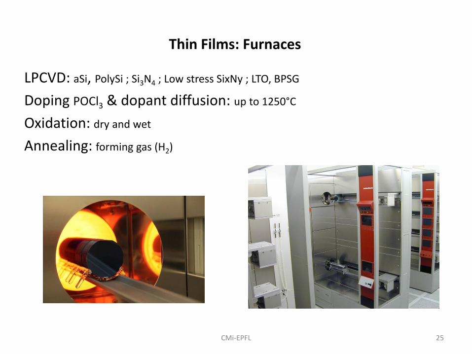
Thin Films: Furnaces
LPCVD: aSi, PolySi ; Si3N4 ; Low stress SixNy ; LTO, BPSG
Doping POCl3 & dopant diffusion: up to 1250°C
Oxidation: dry and wet
Annealing: forming gas (H2)
25

CMi-EPFL
Thin Films: PVD materials available
LAB 600 H EVA 600 EVA 760 Vaco 250 Spider 600 DP 650 BAS 450
Ag Ag Al Ag Al Ag Al
Al Al Au AgCl Al:Si 1% Al Al:Si 0.5%
Al2O
3Au Cr Al Al:Si 2% Al:Si 1.0% Al:Si 0.8%
Au Bi Ti Au Al:Si 4% Au Al:Si 1.0%
Cr Co Bi Al2O
3Cr Al:Si 1.2%
Ge Cr Cr AlN Cu Al:Si 1.5%
In Cu Cu AlScN IGZO Al:Cu:Si 4%,1%
ITO Fe In GeO2
Mo Au
La2O
3Ni MoO
3ITO Ni Cr
MgO NiCr 19% MgO Pd Cu
Mo NiFe 19% Mo Pt Hf
Nb Sn Nb Si Mo
Ni Ti Pt Ta Nb
NiFe 19% Y Ru TaN Pd
Pd RuOx
Ti Pt
Pt Si TiN Sb
SiO2
SiO2
TiO2
Ta
Ta Ta W Ti
Ti Ta2O
5W:Ti 10% W
Ti2O
3Ti WSi
2
Ti3O
5TiN W:Ti 10%
Y TiO2
Zr
Y2O
3TiO
xSiO
2
ZrO2
V2O
5Si
W TiO2
26

CMi-EPFL
Thin Films: Sputtering
• BAS 450
• SPIDER 600
• DP 650
27

CMi-EPFL
Thin Films: Evaporation
• EVA600
• LAB600
• EVA760
28
CMi-EPFL
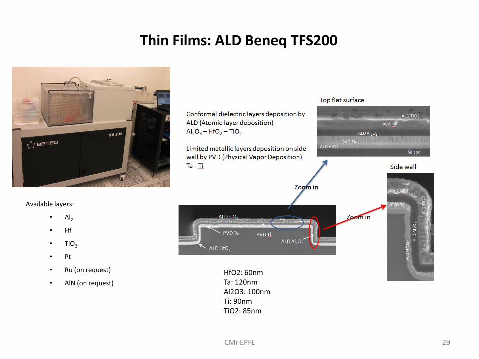
Thin Films: ALD Beneq TFS200
Available layers:
• Al2
• Hf
• TiO2
• Pt
• Ru (on request)
• AlN (on request)
29
HfO2: 60nmTa: 120nmAl2O3: 100nmTi: 90nmTiO2: 85nm

CMi-EPFL
Plasma Etching and IBE
• STS Multiplex ICP (1997): metal etcher
• TEL Unity Me (2017 refurbished): DRM (100sccm), SCCM (200mm)
• AMS200 (2005): DRIE etcher (SOI, high AR, low ARDE)
• SPTS APS (2012): new dielectric etcher
• VEECO IBE NEXUS 350 (2013)
30
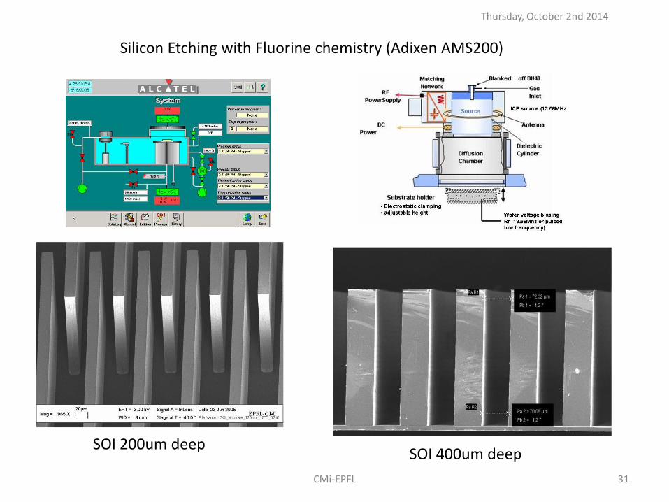
Silicon Etching with Fluorine chemistry (Adixen AMS200)
SOI 200um deepSOI 400um deep
CMi-EPFL
Thursday, October 2nd 2014
31

Silicon Etching with Fluorine chemistry (AMS200)
High AR etching (37:1)of submicron features
Nanopillars in Si (57nm diam. 600nm high)
CMi-EPFL 32

Dielectric Etching (SPTS APS)
Deep Fused silca etching Deep Pyrex etching
CMi-EPFL 33
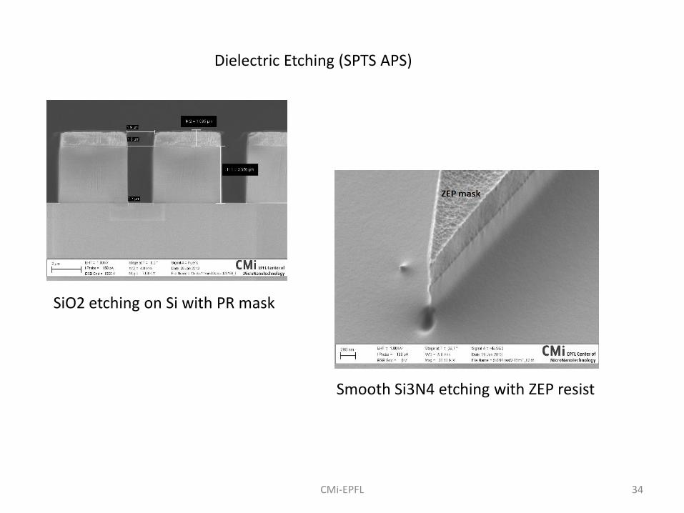
Dielectric Etching (SPTS APS)
Smooth Si3N4 etching with ZEP resist
SiO2 etching on Si with PR mask
CMi-EPFL 34

RIE etching (STS Multiplex ICP)
Al etching (Cl2/BCl3)Polyimide deep etching (O2)
Si submicron features (HBr/O2)
200nm
CMi-EPFL 35

IBE etching (Veeco Nexus IBE 350)
CMi-EPFL
• Etch accuracy: adjustable ER + shutter• ER uniformity: less than 2% (100mm wafers, 49 points, 8mm edge exclusion)
36

Wide variety of material
IBE etching (Veeco Nexus IBE 350)
CMi-EPFL
1um Pt
Si
Thick Pt etch in IBE
37
CMi-EPFL
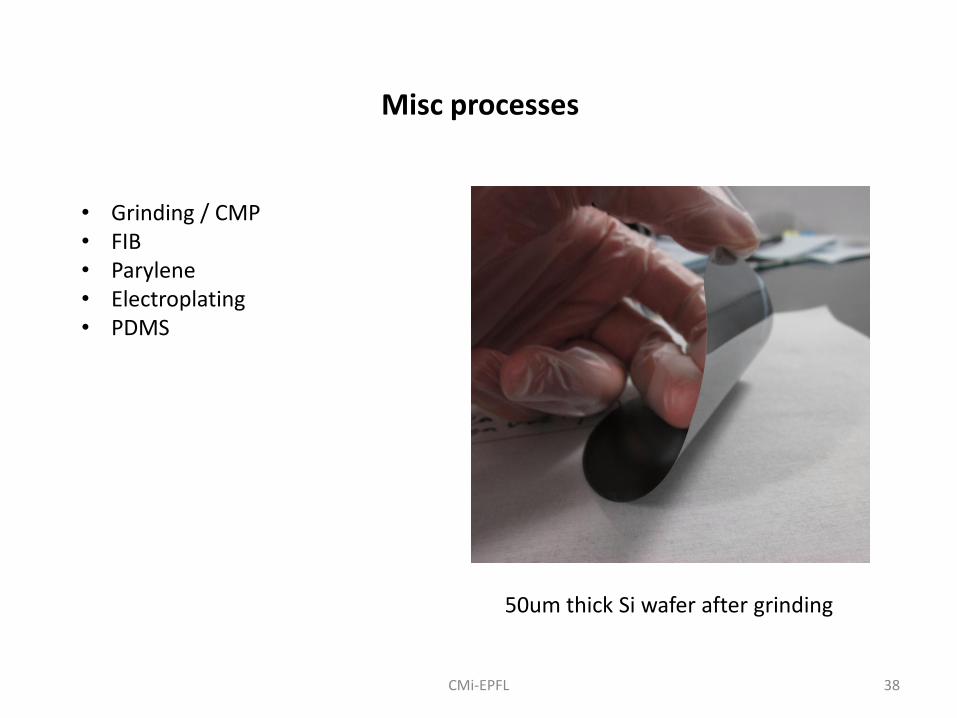
Misc processes
50um thick Si wafer after grinding
• Grinding / CMP• FIB• Parylene• Electroplating• PDMS
38
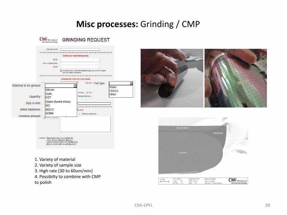
1. Variety of material2. Variety of sample size3. High rate (30 to 60um/min)4. Possibilty to combine with CMPto polish
Misc processes: Grinding / CMP
CMi-EPFL 39
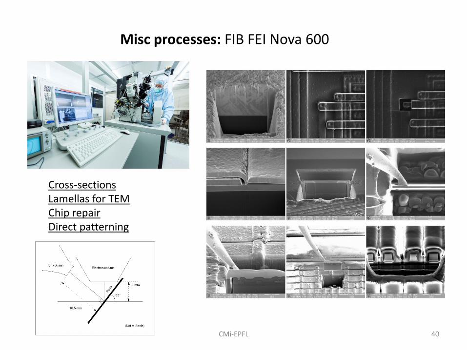
Misc processes: FIB FEI Nova 600
CMi-EPFL
Cross-sectionsLamellas for TEMChip repairDirect patterning
40

Misc processes: Parylene
CMi-EPFL
1. Stop layer2. Fonctional layer3. Bonding layer4. Sealing layer5. Biocomp, Room T, conformal…6. Any shape can be coated…7. More than 50 projects rely on parylene
41
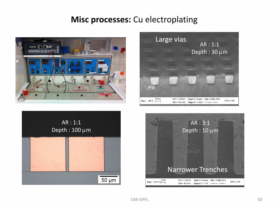
Misc processes: Cu electroplating
CMi-EPFL
Narrow Trenches
Large viasAR : 1:1
Depth : 30 mm
AR : 3:1Depth : 10 mm
Narrower Trenches
AR : 1:1Depth : 100 mm
42
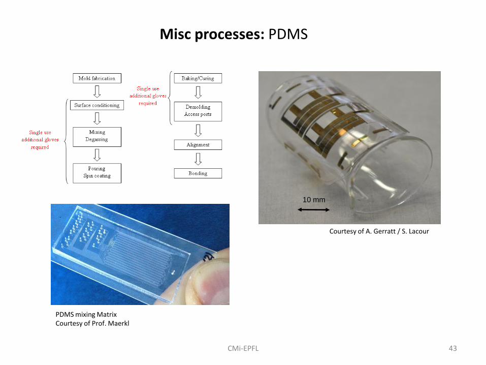
Misc processes: PDMS
CMi-EPFL
Large viasAR : 1:1
Depth : 30 mm
AR : 3:1Depth : 10 mm
AR : 1:1Depth : 100 mm
10 mm
Courtesy of A. Gerratt / S. Lacour
PDMS mixing MatrixCourtesy of Prof. Maerkl
43

CMi-EPFL
Metrology
44
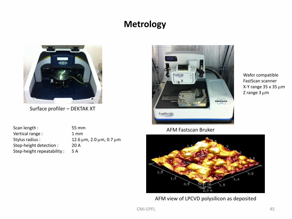
CMi-EPFL
Metrology
Surface profiler – DEKTAK XT
Scan length : 55 mm Vertical range : 1 mmStylus radius : 12.6 mm, 2.0 mm, 0.7 mmStep-height detection : 20 AStep-height repeatability : 5 A
Wafer compatibleFastScan scannerX-Y range 35 x 35 mmZ range 3 mm
AFM Fastscan Bruker
AFM view of LPCVD polysilicon as deposited
45

Metrology: SEM + EDX analysis
Material characterization (EDX)
3 state of the art SEMs available in CMi: LEO1550, Zeiss Merlin and FEI (FIB)
CMi-EPFL
Thursday, October 2nd 2014
46

CMi-EPFL
Example 1: Damascene process
Technologies: Polyimide coating and anisotrpic dry etching,
diffusion barrier /seed layer
Cooper electroplating,
Cooper CMP,
4um copper embedded in 4um lowK Polyimide (EPFL-CMI source)
47
CMi-EPFL
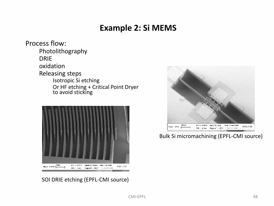
Example 2: Si MEMS
Process flow:PhotolithographyDRIEoxidationReleasing steps
Isotropic Si etchingOr HF etching + Critical Point Dryer to avoid sticking
Bulk Si micromachining (EPFL-CMI source)
SOI DRIE etching (EPFL-CMI source)
48
CMi-EPFL
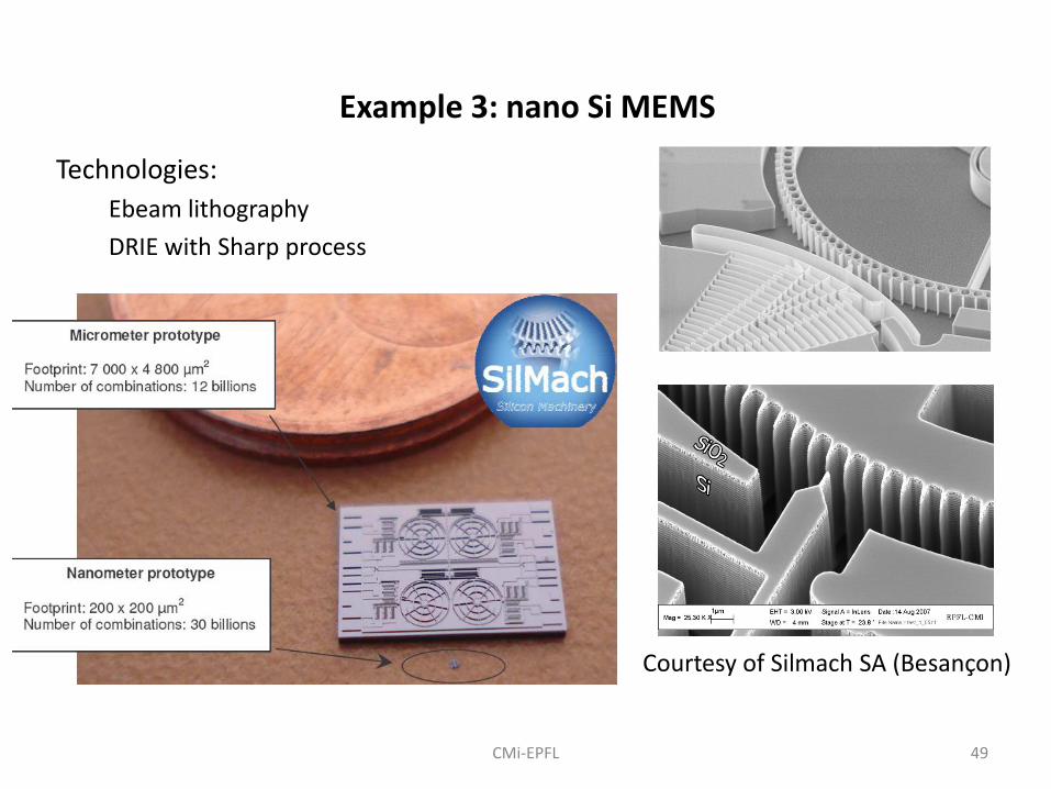
Example 3: nano Si MEMS
Technologies:
Ebeam lithography
DRIE with Sharp process
Courtesy of Silmach SA (Besançon)
49

CMi-EPFL
Example 4: shadow masks
Shadow mask
Resolution Aspect Material Technique Alignment
Low(500µm)
Flexible Kapton foil Automaticcutter
No
Medium(10µm)
Rigid Silicon bulk DRIE+ grinding
Yes(10µm)
High(200nm)
Rigid SiN membrane RIE+ wet etching
Yes(1µm)
Direct deposition/patterning technique- No resist mask- No subsequent etching- Targeted deposition
Metalevaporation
Substrate
Metal source
Back side: Si KOH etch to SiNKapton foil
Silicon bulk 50

ÉC OLE PO LY TEC H NIQ U EFÉ DÉRALE D E LAUSAN NE
THANKS FOR YOUR ATTENTION
51
CMi-EPFL
51
CMi-EPFL


