
5/16/2012
1
FPGA Architecture
EE216B: VLSI Signal Processing
Prof. Dejan Marković [email protected]
Outline
FPGA Architecture
– Logic-Block Architecture
– Routing Architecture and Techniques
– Interconnect Switches
Xilinx FPGAs
– Overview
– Technological side effects (65nm)
– Virtex-5 FPGAs
References
13.2
Slide material from R. Yap & M. Ali (Spring 2008)
5/16/2012
2
FPGA Architecture
FPGA = Field-Programmable Gate Array
Basic elements
Logic-block architecture
Routing architecture
– Layout
–Routing techniques
– Interconnect switches
13.3
Logic-Block Architecture
Granularity classifications
Fine grain
Coarse grain
13.4
5/16/2012
3
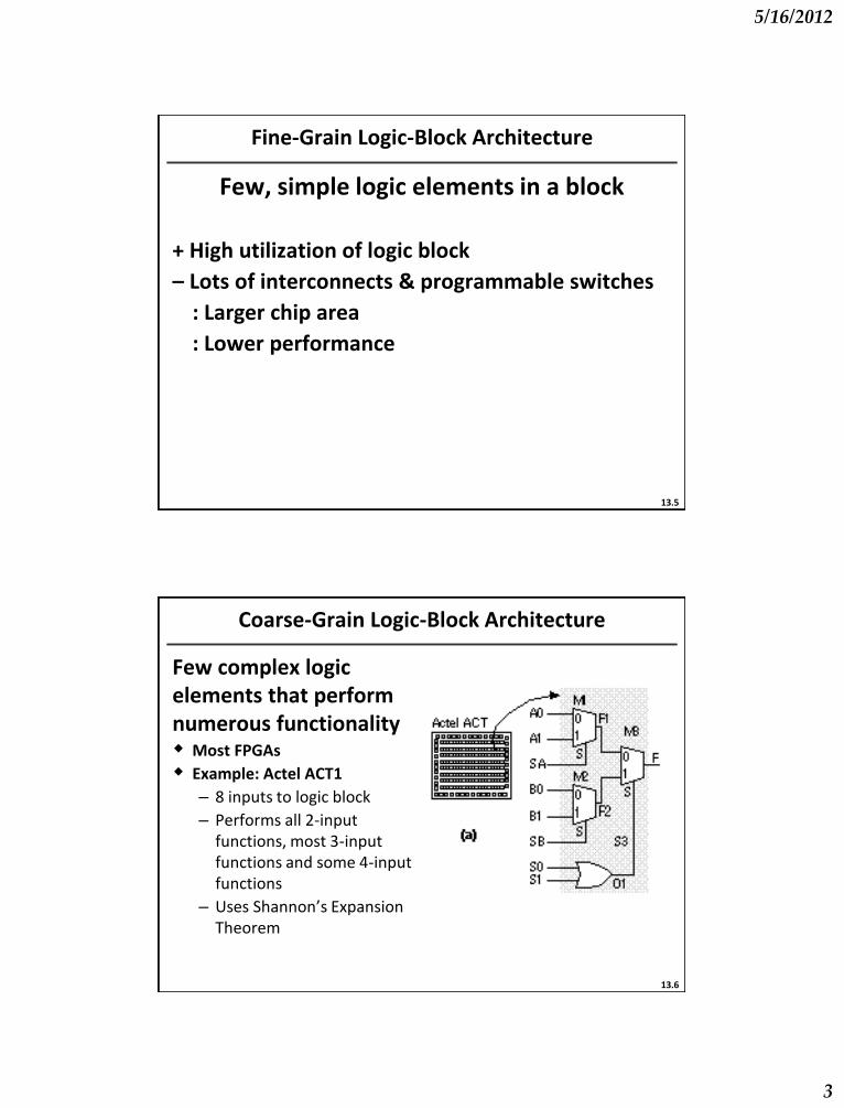
Fine-Grain Logic-Block Architecture
Few, simple logic elements in a block
+ High utilization of logic block
– Lots of interconnects & programmable switches
: Larger chip area
: Lower performance
13.5
Coarse-Grain Logic-Block Architecture
Few complex logic elements that perform numerous functionality Most FPGAs
Example: Actel ACT1
– 8 inputs to logic block
– Performs all 2-input functions, most 3-input functions and some 4-input functions
– Uses Shannon’s Expansion Theorem
13.6
5/16/2012
4
Outline
13.7
FPGA Architecture
– Logic-Block Architecture
– Routing Architecture and Techniques
– Interconnect Switches
Xilinx FPGAs
– Overview
– Technological side effects (65nm)
– Virtex-5 FPGAs
References
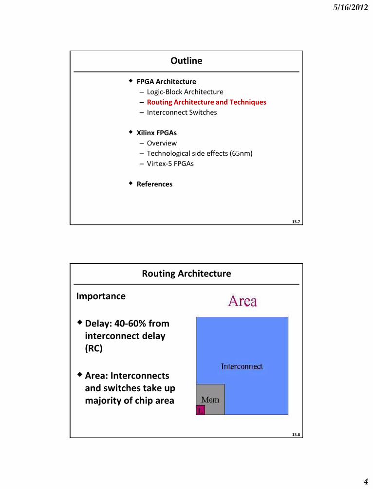
Routing Architecture
Importance
Delay: 40-60% from interconnect delay (RC)
Area: Interconnects and switches take up majority of chip area
13.8

5/16/2012
5
Layout (Row-based)
Type 1: Row Based
– Cells located adjacent to routing channel
– Horizontal routing channel
– Estimating optimum number of tracks and segments difficult
– Main tradeoff: performance vs. routability
13.9
single
double long
Routing Techniques (Row-based)
Fully-segmented channel
– Switches needed between every cross-point
– Flexible routing
– Many switches
13.10
5/16/2012
6
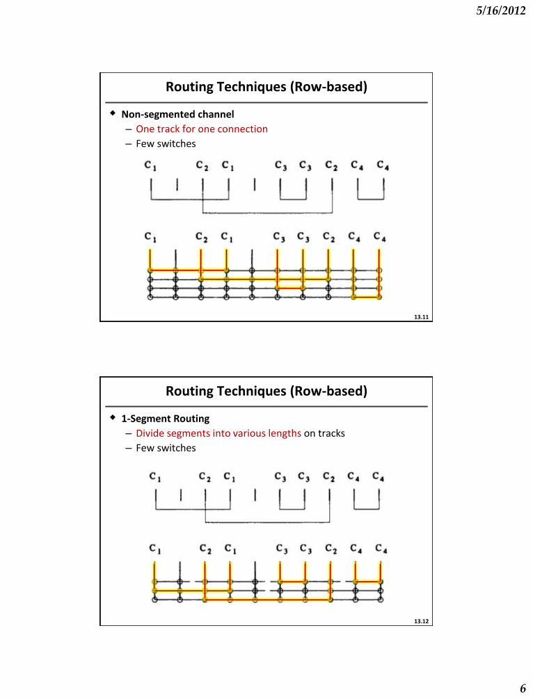
Routing Techniques (Row-based)
Non-segmented channel
– One track for one connection
– Few switches
13.11
Routing Techniques (Row-based)
1-Segment Routing
– Divide segments into various lengths on tracks
– Few switches
13.12
5/16/2012
7
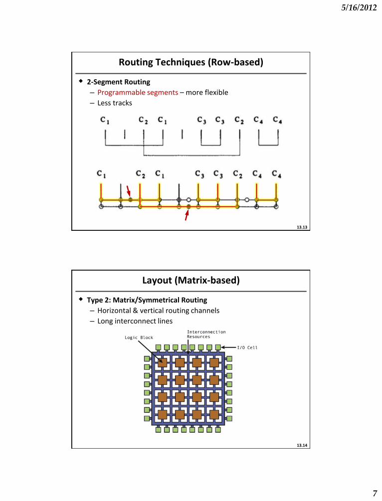
Routing Techniques (Row-based)
2-Segment Routing
– Programmable segments – more flexible
– Less tracks
13.13
Layout (Matrix-based)
Type 2: Matrix/Symmetrical Routing
– Horizontal & vertical routing channels
– Long interconnect lines
13.14
5/16/2012
8
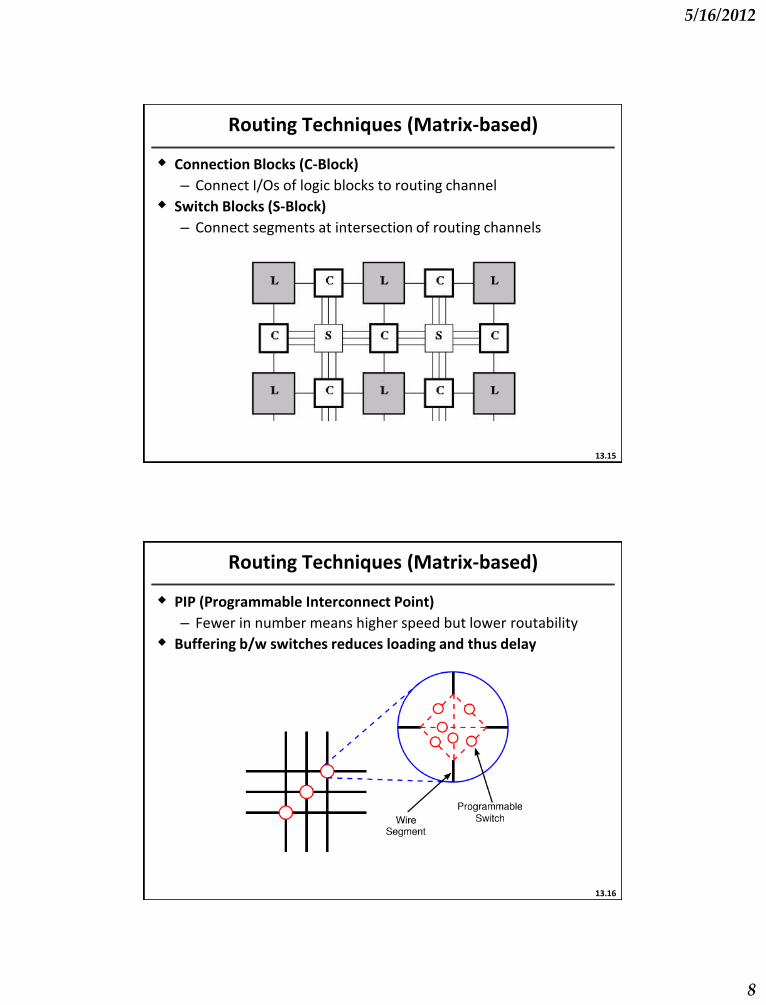
Routing Techniques (Matrix-based)
Connection Blocks (C-Block)
– Connect I/Os of logic blocks to routing channel
Switch Blocks (S-Block)
– Connect segments at intersection of routing channels
13.15
Routing Techniques (Matrix-based)
PIP (Programmable Interconnect Point)
– Fewer in number means higher speed but lower routability
Buffering b/w switches reduces loading and thus delay
13.16

5/16/2012
9
CLB
LUT LUT
LUT LUT
CLB
LUT LUT
LUT LUT
Switch box
Connection box 2D-Mesh Interconnects
13.17
• From O(N
2) complexity
• Full connectivity impractical
2D-Mesh is NOT Scalable
CLB
LUT LUT
LUT LUT
13.18

5/16/2012
10
Tree of Meshes Butterfly Fat Tree
From: A. DeHon, VLSI 10/2004.
Hierarchical Networks
Limited connectivity N
2
N
Excess delay
13.19
Outline
13.20
FPGA Architecture
– Logic-Block Architecture
– Routing Architecture and Techniques
– Interconnect Switches
Xilinx FPGAs
– Overview
– Technological side effects (65nm)
– Virtex-5 FPGAs
References
5/16/2012
11
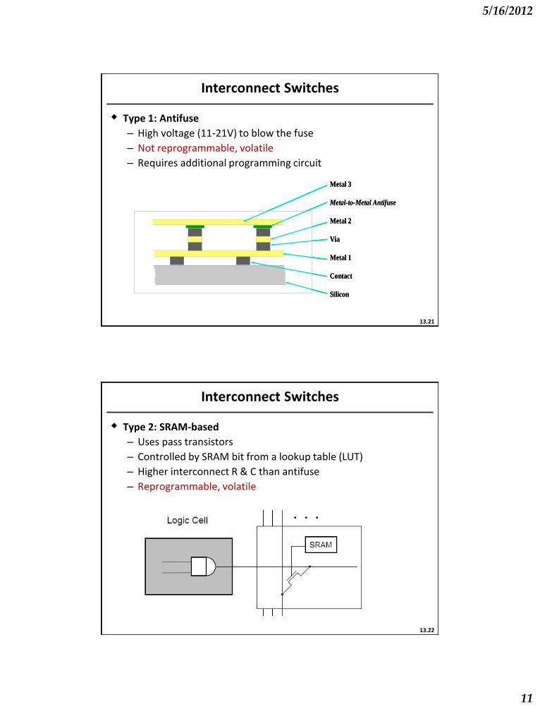
Interconnect Switches
Type 1: Antifuse
– High voltage (11-21V) to blow the fuse
– Not reprogrammable, volatile
– Requires additional programming circuit
Metal 3
Metal-to-Metal Antifuse
Metal 2
Via
Metal 1
Contact
Silicon
Metal 3
Metal-to-Metal Antifuse
Metal 2
Via
Metal 1
Contact
Silicon
13.21
Interconnect Switches
Type 2: SRAM-based
– Uses pass transistors
– Controlled by SRAM bit from a lookup table (LUT)
– Higher interconnect R & C than antifuse
– Reprogrammable, volatile
13.22

5/16/2012
12
Interconnect Switches
Type 3: EPROM-based
– Uses floating gate transistor
– Turns OFF by injecting charge on the gate
– Memory retained when power is down
– Reprogrammable, non-volatile
13.23
Outline
13.24
FPGA Architecture
– Logic-Block Architecture
– Routing Architecture and Techniques
– Interconnect Switches
Xilinx FPGAs
– Overview
– Technological side effects (65nm)
– Virtex-5 FPGAs
References
5/16/2012
13
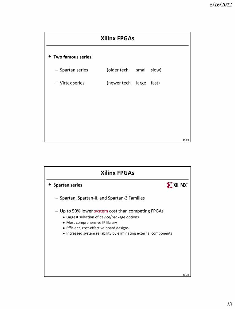
Xilinx FPGAs
Two famous series
– Spartan series (older tech small slow)
– Virtex series (newer tech large fast)
13.25
Xilinx FPGAs
Spartan series
– Spartan, Spartan-II, and Spartan-3 Families
– Up to 50% lower system cost than competing FPGAs ● Largest selection of device/package options
● Most comprehensive IP library
● Efficient, cost-effective board designs
● Increased system reliability by eliminating external components
13.26
5/16/2012
14
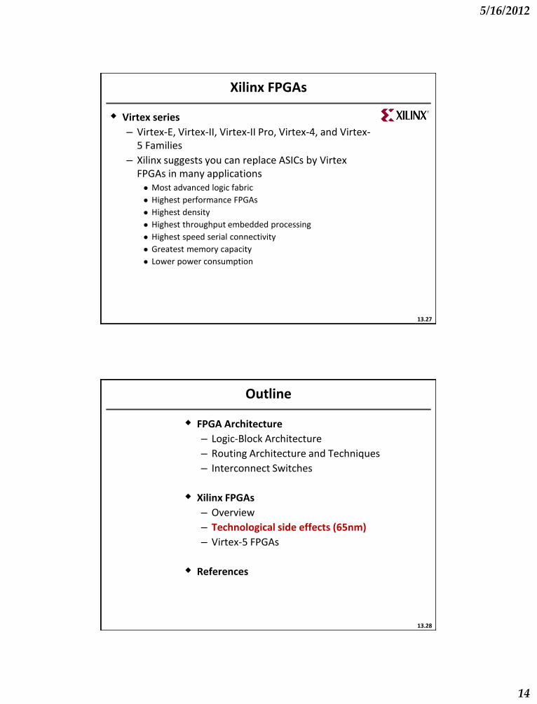
Xilinx FPGAs
Virtex series
– Virtex-E, Virtex-II, Virtex-II Pro, Virtex-4, and Virtex-5 Families
– Xilinx suggests you can replace ASICs by Virtex FPGAs in many applications ● Most advanced logic fabric
● Highest performance FPGAs
● Highest density
● Highest throughput embedded processing
● Highest speed serial connectivity
● Greatest memory capacity
● Lower power consumption
13.27
Outline
13.28
FPGA Architecture
– Logic-Block Architecture
– Routing Architecture and Techniques
– Interconnect Switches
Xilinx FPGAs
– Overview
– Technological side effects (65nm)
– Virtex-5 FPGAs
References
5/16/2012
15
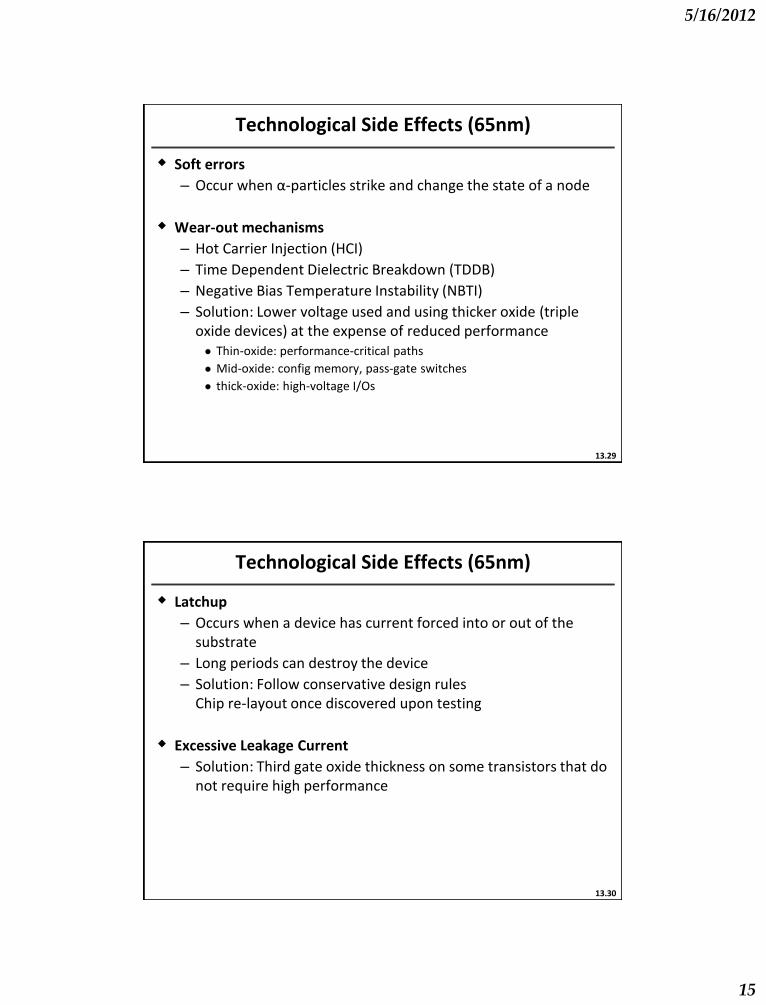
Technological Side Effects (65nm)
Soft errors
– Occur when α-particles strike and change the state of a node
Wear-out mechanisms
– Hot Carrier Injection (HCI)
– Time Dependent Dielectric Breakdown (TDDB)
– Negative Bias Temperature Instability (NBTI)
– Solution: Lower voltage used and using thicker oxide (triple oxide devices) at the expense of reduced performance ● Thin-oxide: performance-critical paths
● Mid-oxide: config memory, pass-gate switches
● thick-oxide: high-voltage I/Os
13.29
Technological Side Effects (65nm)
Latchup
– Occurs when a device has current forced into or out of the substrate
– Long periods can destroy the device
– Solution: Follow conservative design rules Chip re-layout once discovered upon testing
Excessive Leakage Current
– Solution: Third gate oxide thickness on some transistors that do not require high performance
13.30
5/16/2012
16
Outline
13.31
FPGA Architecture
– Logic-Block Architecture
– Routing Architecture and Techniques
– Interconnect Switches
Xilinx FPGAs
– Overview
– Technological side effects (65nm)
– Virtex-5 FPGAs
References
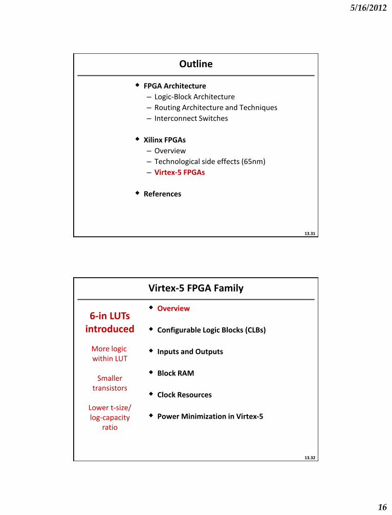
Virtex-5 FPGA Family
Overview
Configurable Logic Blocks (CLBs)
Inputs and Outputs
Block RAM
Clock Resources
Power Minimization in Virtex-5
13.32
6-in LUTs introduced
More logic within LUT
Smaller
transistors
Lower t-size/ log-capacity
ratio
5/16/2012
17
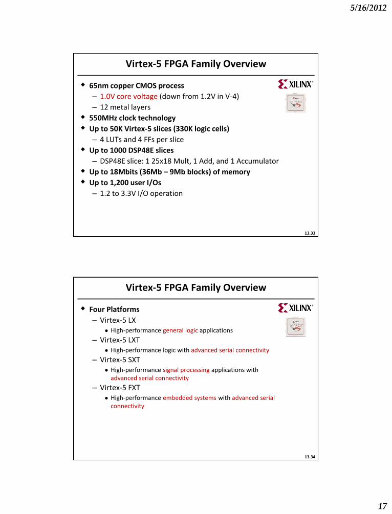
Virtex-5 FPGA Family Overview
65nm copper CMOS process
– 1.0V core voltage (down from 1.2V in V-4)
– 12 metal layers
550MHz clock technology
Up to 50K Virtex-5 slices (330K logic cells)
– 4 LUTs and 4 FFs per slice
Up to 1000 DSP48E slices
– DSP48E slice: 1 25x18 Mult, 1 Add, and 1 Accumulator
Up to 18Mbits (36Mb – 9Mb blocks) of memory
Up to 1,200 user I/Os
– 1.2 to 3.3V I/O operation
13.33
Virtex-5 FPGA Family Overview
Four Platforms
– Virtex-5 LX ● High-performance general logic applications
– Virtex-5 LXT ● High-performance logic with advanced serial connectivity
– Virtex-5 SXT ● High-performance signal processing applications with
advanced serial connectivity
– Virtex-5 FXT ● High-performance embedded systems with advanced serial
connectivity
13.34

5/16/2012
18
Virtex-5 FPGA Family Overview
13.35
100K 200K 300K
Logic Cells
400
800
1200 D
SP4
8E
Slic
es
LX/LXT
FXT
SXT
Virtex-5 FPGA Family Overview
13.36
5/16/2012
19
Virtex-5 FPGA Family
13.37
Overview
Configurable Logic Blocks (CLBs)
Inputs and Outputs
Block RAM
Clock Resources
Power Minimization in Virtex-5
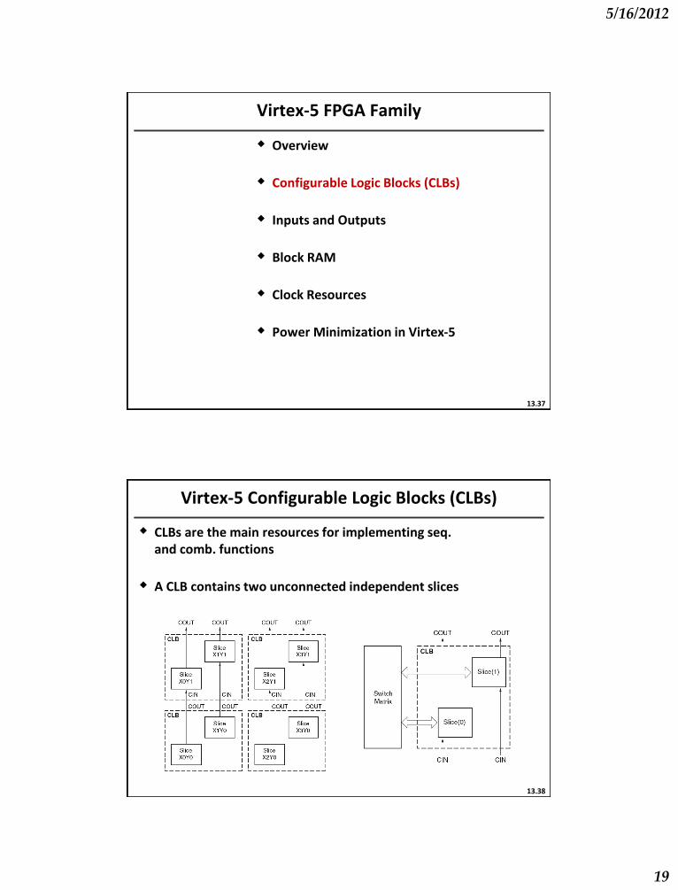
Virtex-5 Configurable Logic Blocks (CLBs)
CLBs are the main resources for implementing seq. and comb. functions
A CLB contains two unconnected independent slices
13.38
5/16/2012
20
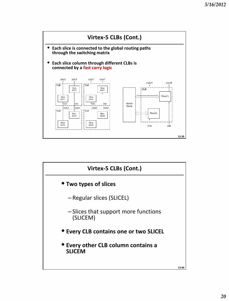
Virtex-5 CLBs (Cont.)
Each slice is connected to the global routing paths through the switching matrix
Each slice column through different CLBs is
connected by a fast carry logic
13.39
Two types of slices
–Regular slices (SLICEL)
– Slices that support more functions (SLICEM)
Every CLB contains one or two SLICEL Every other CLB column contains a
SLICEM
Virtex-5 CLBs (Cont.)
13.40
5/16/2012
21
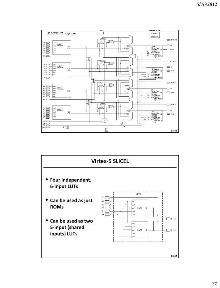
Virtex-5 FPGA Family SLICEL Diagram
13.41
Four independent, 6-input LUTs
Can be used as just ROMs
Can be used as two 5-input (shared inputs) LUTs
Virtex-5 SLICEL
13.42

5/16/2012
22
Fast Lookahead Carry Logic
– Dedicated carry logic
– Carry chain is running upward through multiple CLBs with 4bits per slice
– S for “propagate” and DI for “generate”
– CYINIT may be used as the first carry bit
Virtex-5 CLBs (Cont.)
13.43
Storage-element configuration
– Edge triggered (+/-) FF or level sensitive (H/L) latch
– Synchronous or asynchronous set/reset (using SR and REV inputs)
– D-inputs from LUTs or using AX, BX, CX, and DX
Virtex-5 CLBs (Cont.)
13.44
5/16/2012
23
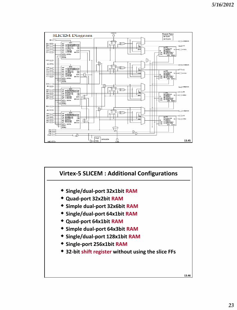
Virtex-5 FPGA Family Configurable Logic Blocks (CLBs)
13.45
Single/dual-port 32x1bit RAM
Quad-port 32x2bit RAM
Simple dual-port 32x6bit RAM
Single/dual-port 64x1bit RAM
Quad-port 64x1bit RAM
Simple dual-port 64x3bit RAM
Single/dual-port 128x1bit RAM
Single-port 256x1bit RAM
32-bit shift register without using the slice FFs
Virtex-5 SLICEM : Additional Configurations
13.46
5/16/2012
24
RAM inside SLICEM are called Distributed RAM
Distributed RAM modules have synchronous input and asynchronous output
The outputs can be synchronous by going through the SLICEM FFs
Virtex-5 CLBs (Cont.)
13.47
Virtex-5 FPGA Family
13.48
Overview
Configurable Logic Blocks (CLBs)
Inputs and Outputs
Block RAM
Clock Resources
Power Minimization in Virtex-5
5/16/2012
25
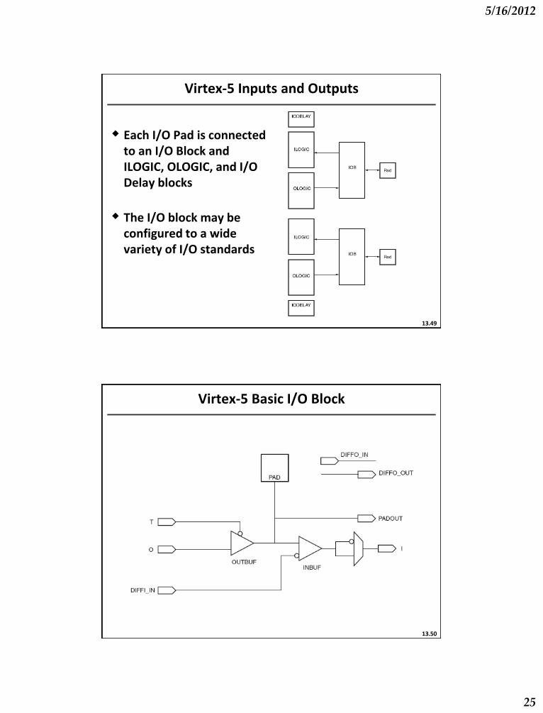
Each I/O Pad is connected to an I/O Block and ILOGIC, OLOGIC, and I/O Delay blocks
The I/O block may be configured to a wide variety of I/O standards
Virtex-5 Inputs and Outputs
13.49
Virtex-5 Basic I/O Block
13.50
5/16/2012
26
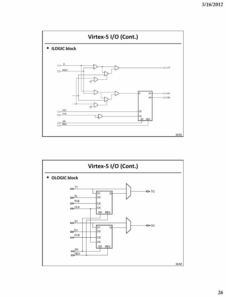
ILOGIC block
Virtex-5 I/O (Cont.)
13.51
OLOGIC block
Virtex-5 I/O (Cont.)
13.52
5/16/2012
27
The I/O Blocks are equipped by Digitally Controlled Impedance (DCI)
– Adjusts the o/p impedance or i/p termination to accurately match the c/c impedance of the PCB transmission line
– Continuously adjusts the impedance compensating the impedance changes due to process variations, temperature, and supply voltage fluctuations
– Provides the parallel or series termination for transmitters and receivers
Virtex-5 I/O (Cont.)
13.53
Virtex-5 FPGA Family
13.54
Overview
Configurable Logic Blocks (CLBs)
Inputs and Outputs
Block RAM
Clock Resources
Power Minimization in Virtex-5
5/16/2012
28
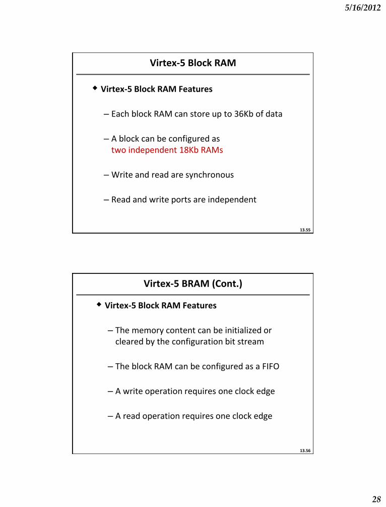
Virtex-5 Block RAM Features
– Each block RAM can store up to 36Kb of data
– A block can be configured as two independent 18Kb RAMs
– Write and read are synchronous
– Read and write ports are independent
Virtex-5 Block RAM
13.55
Virtex-5 Block RAM Features
– The memory content can be initialized or cleared by the configuration bit stream
– The block RAM can be configured as a FIFO
– A write operation requires one clock edge
– A read operation requires one clock edge
Virtex-5 BRAM (Cont.)
13.56

5/16/2012
29
Virtex-5 FPGA Family
13.57
Overview
Configurable Logic Blocks (CLBs)
Inputs and Outputs
Block RAM
Clock Resources
Power Minimization in Virtex-5
Global Clocks
– Each Virtex-5 device has 32 global Clk lines
– It can clock all sequential resources (CLBs, Block RAMs, and I/Os)
– Global Clk lines driven by a global Clk buffer ● Can be used as a clock enable
● Can select between two clock sources
– A global clock buffer is driven by a Clock Management Tile (CMT) that adjusts the clock delay relative to another clock
Virtex-5 Clock Resources
13.58

5/16/2012
30
Regional Clocks
– A Virtex-5 device is divided into regions (8 to 24)
– Each region has two regional clock buffers and four regional clock trees
– Each region is assigned an I/O bank that has four clock-capable clock inputs
– A regional clock buffer can divide the incoming clock rate by any integer number from 1 to 8
– A regional clocks can drive regional clock trees from the adjacent regions
Virtex-5 Clocks (Cont.)
13.59
Virtex-5 FPGA Family
13.60
Overview
Configurable Logic Blocks (CLBs)
Inputs and Outputs
Block RAM
Clock Resources
Power Minimization in Virtex-5

5/16/2012
31
Power Minimization in Virtex-5
Static power Challenges
– High leakage current across the channel or through the gate oxide
13.61
Power Minimization in Virtex-5 (Cont.)
Static power reduction
– Triple Oxide Process Technology
● Normally FPGAs use very thin oxide transistors for high performance (High leakage), and thicker for the high voltage tolerant transistors in the I/O blocks
● The triple oxide is to introduce a third medium-thickness gate oxide
● The triple oxide process opens up the opportunities to use the right transistor for the right job
13.62

5/16/2012
32
Power Minimization in Virtex-5 (Cont.)
Static power reduction
– Triple Oxide Process Technology
● The thin oxide used for the core logic
● The thick oxide used for the I/O blocks
● The mid-oxide transistors have lower performance and dramatically reduced leakage compared to thin oxide transistors and used in:
– The configuration memory (no need for high perf)
– Pass gates used in routing (no need for fast switching)
13.63
Power Minimization in Virtex-5 (Cont.)
Static power reduction
– The use of 6-inputs LUTs (for the first time) allows increase of logic capacity
– More logic happens locally
– Less drivers needed and hence less leakage
13.64
5/16/2012
33
Power Minimization in Virtex-5 (Cont.)
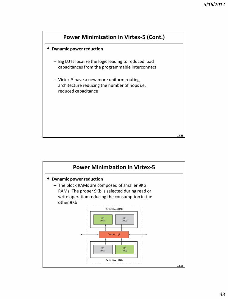
Dynamic power reduction
– Big LUTs localize the logic leading to reduced load capacitances from the programmable interconnect
– Virtex-5 have a new more uniform routing architecture reducing the number of hops i.e. reduced capacitance
13.65
Power Minimization in Virtex-5
Dynamic power reduction
– The block RAMs are composed of smaller 9Kb RAMs. The proper 9Kb is selected during read or write operation reducing the consumption in the other 9Kb
13.66
5/16/2012
34
References
Virtex-5 FPGA User Guide (xilinx.com)
Virtex-5 Family Overview (xilinx.com)
http://en.wikipedia.org/wiki/Field-programmable_gate_array
http://www.ecs.umass.edu/ece/tessier/courses/697ff/lect13-ece697f.ppt
http://www.eecg.toronto.edu/~vaughn/challenge/fpga_arch.html
http://www.chipdesignmag.com/print.php?articleId=434?issueId=16
http://www.cs.cmu.edu/afs/cs.cmu.edu/academic/class/15828-s98/lectures/0119/index.htm
http://www.edacafe.com/books/ASIC/Book/CH05/CH05.1.php
W.-K. Mak and D.F. Wong, “Channel Segmentation Design for Symmetrical FPGAs”, ICCD 1997, pp. 496-501.
Stephen Brown and Jonathan Rose, “Architecture of FPGAs and CPLDs: A Tutorial”, (Univ. of Toronto)
Ashok K. Sharma, “Programmable Logic Handbook”, 1998
Derek Curd, “Power Consumption In 65nm FPGAs”, Xilinx WP246 (V1.2) February 1, 2007
* Available on classwiki
13.67


