
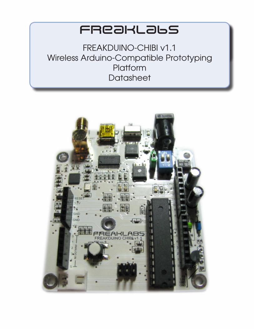
FreakLabs FREAKDUINO-CHIBI v1.1
Wireless Arduino-Compatible Prototyping Platform
Datasheet

Page 1FREAKDUINO-CHIBI v1.1B
Document Revision History
Date Description2010-11-01 v1.1A Document creation2010-12-26 v1.1B
Added power switch matrix in Connectors/Jumpers/Switches sectionAdded troubleshooting section

Page 2FREAKDUINO-CHIBI v1.1B
SpecificationsThe FreakLabs FREAKDUINO-CHIBI board is designed for rapid prototyping, evaluation, and deployment of custom wireless devices at low cost. It combines the ease-of-use of the Arduino IDE and toolchain, compatibility with a rich assortment of peripherals in the Arduino shield form factor, and an integrated IEEE 802.15.4 wireless radio for inexpensive prototyping and testing of a wireless device.
The base board has all the functionality of an Arduino-based system with wireless communication and is an inexpensive way to start playing with wireless Arduino designs.
It also has optional features such as battery regulation circuitry, a low-cost bottom-mounted battery case, or a ruggedized enclosure with integrated battery case.
This board is designed to introduce people to wireless sensor networking inexpensively and with-out having to deal with complex toolchains, protocol stacks, and software. It’s fully compatible with the Arduino IDE and toolchain which offers a single click compile and download and a rich ecosystem of open source software and tutorials available on the internet. The electrical specifica-tions and connector form factor are also compatible with the original Arduino hardware so that the board can interface with the large assortment of Arduino peripheral shields. The availability
QuicK SpecS
MCU: ATMega328P
Memory: 32 kB Flash/2 kB RAM
Communications: 802.15.4 wireless, USB
Expansion: Ardu-ino-compatible shield connector
Power: Ext 5VDC, USB, Battery (op-tional)
Options: Rugge-dized enclosure, battery regulation circuit, standalone battery case
Page 2FREAKDUINO-CHIBI v1.1B

Page 3FREAKDUINO-CHIBI v1.1B
of third party peripheral shields and open source software allows this board to be used for many diverse applications.
Enhancements were also added to this board to increase functionality. The addition of an inte-grated wireless radio based on the 802.15.4 protocol (same radio protocol as the XBee) allows for wireless control of devices or wireless sensor data collection. Battery circuitry was added so that it could function as a true wireless node without any external power cables. The board is also fitted to a ruggedized enclosure so that the design can be transported safely or deployed in remote set-tings without worrying about damaging the circuit.
RadioThe main addition to this board is the integrated wireless radio. The radio is based on the 802.15.4 wireless protocol and is the same protocol used by XBee modules and Zigbee devices. The radio operates at 2.4 GHz and comes with an RP-SMA antenna connector which is a stan-dard antenna connector commonly found on Wi-Fi routers. An external antenna was chosen over other options such as a chip antenna or printed antenna because of the improved range and variety of available antennas.
The radio driver software and protocol stack are fully open source and available as an Arduino library. The protocol stack is simplified to three main library functions to make wireless commu-nications as simple as possible. Those functions are: init, send, and receive. This makes it easy to use the radio as a simple extension of a serial port or to set up a peer-to-peer star network where each device can talk with any other device within listening range.
There are also many benefits to using 802.15.4 for communications. At 2.4 GHz, the antennas used are the same as those used for Wi-Fi. Hence there are a large variety of antennas in different sizes, shapes, and power. Omnidirectional antennas such as the standard whip antennas on Wi-Fi routers give moderate range and allow transmission from all directions. Directional antennas can also be used for greatly improved range if the direction of communications is fixed.
Some other benefits of using 802.15.4 is robustness such as automatic acknowledge and retries

Page 4FREAKDUINO-CHIBI v1.1B
and functionality such as auto-discard of frames that don’t match the particular network address or node address.
Also, since it’s possible to talk directly to the radio, it also allows for more flexibility for advanced users such as a direct readout of the signal strength (RSSI), changing transmission thresholds (CCA), number of retries, or whatever else is available in the radio’s registers.

Page 5FREAKDUINO-CHIBI v1.1B
PowerThere are three options to provide power to the board. The most common is via the USB, how-ever the board can also be powered via an external adapter connected to the DC jack. This is especially useful when more power is needed than can be provided by the USB. Finally, when no external power is available, the board can also be battery powered.
The USB connector provides up to 500 mA of current at 5V and can directly power the board for most applications. It’s convenient when the device is connected to a PC since the USB to serial converter also allows for communications with the PC.
For designs with higher current requirements, such as driving motors or high power LEDs, an ex-ternal DC adapter can be used. The adapter should be a minimum of 6V and a maximum of 10V.
Note: The power input is determined by the position of the jumper below the DC input jack. The markings on the jumper indicate whether the USB or DC input is being used.
The board also has two separate connectors for batteries. One of the connectors allows a battery case to be mounted on the bottom side of the board. This is convenient since the battery case is directly mounted to the board and allows for battery operation in tight spaces.
The other connector is located near the bottom of the board and is a 2-wire connector that fea-tures mating and polarization. It’s technically called a JST XH series connector and was chosen to allow easy attachment of external battery cables without worrying about reversing the positive and negative connections. It also makes connecting and disconnecting the battery case of the enclo-sure to the board much easier.
There is also a battery regulation circuit on the board. The reason this is needed is because the battery voltage varies based on the battery type and amount of charge left. The voltage regulation allows any type of battery to be connected to the board as long as the battery voltage is below 6V and will generate a stable 5V output. The battery regulation circuit has a maximum current out-put of 200 mA. This is fine for most devices, however devices like motors and high power LEDs (1W or greater) may exceed the maximum current output.
There is a power switch on the board that selects between external line power (via USB or DC jack depending on the jumper) or battery power. The switch can also be used as an OFF switch if either line power or battery power is not present.
There is also a 2-pin DIP switch on the board that enables or disables the power LED and the auxiliary LED. If the board is externally powered, then it’s fine to enable both LEDs, but when the board is battery powered, the LEDs will cause the battery to drain much faster. The DIP switch allows the user to easily disable the LEDs during battery operation.
Page 6FREAKDUINO-CHIBI v1.1B
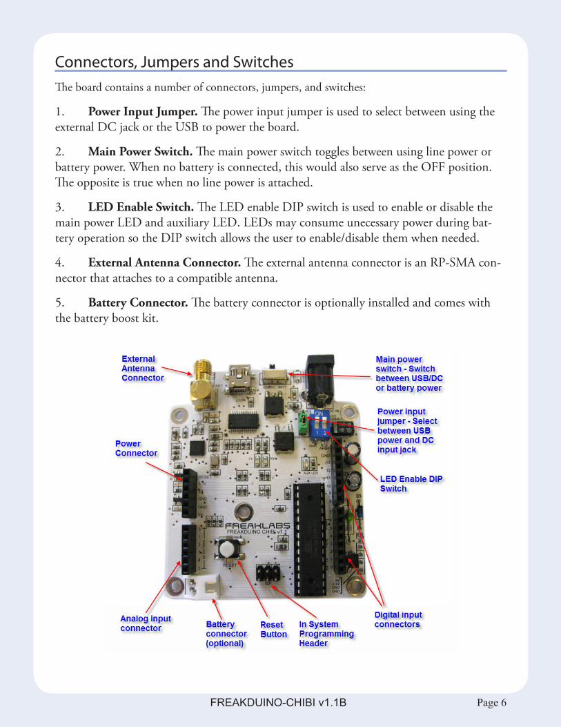
Connectors, Jumpers and SwitchesThe board contains a number of connectors, jumpers, and switches:
1. Power Input Jumper. The power input jumper is used to select between using the external DC jack or the USB to power the board.
2. Main Power Switch. The main power switch toggles between using line power or battery power. When no battery is connected, this would also serve as the OFF position. The opposite is true when no line power is attached.
3. LED Enable Switch. The LED enable DIP switch is used to enable or disable the main power LED and auxiliary LED. LEDs may consume unecessary power during bat-tery operation so the DIP switch allows the user to enable/disable them when needed.
4. External Antenna Connector. The external antenna connector is an RP-SMA con-nector that attaches to a compatible antenna.
5. Battery Connector. The battery connector is optionally installed and comes with the battery boost kit.

Page 7FREAKDUINO-CHIBI v1.1B
Due to having three ways to power the board, the power switch and power jumper settings need to be configured for your desired input. The switch and jumper is labeled to make things easy, but here’s a quick reference chart on how to configure the power input. The positions in the table cor-respond to the labels on the board.
Main Power Switch Power Input JumperUSB Power USB/DC USB PWRExternal DC Power USB/DC DC PWRBattery Power BATT Ignored
Uploading CodeCompiling and uploading user code into the Freakduino board is very simple:
1. Download the Arduino IDE. The first thing you need to do is get the Arduino IDE and install it. It can be found at the Arduino site.
2. Open the IDE and add code. We’re going to take a shortcut and open up one of the default examples that comes with the Arduino software. Go to the “File/Examples/Ba-sics” menu and select “Blink”.
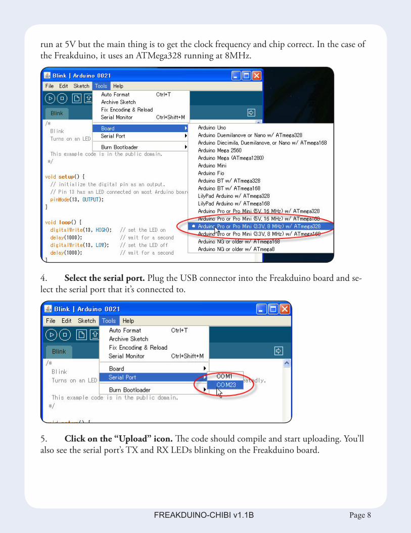
3. Select the board. Go to the “Tools/Board” menu and select “Arduino Pro or Pro Mini (3.3V, 8 MHz) w/ATMega328”. Don’t worry that it specifies 3.3 volts. We actually
Page 8FREAKDUINO-CHIBI v1.1B
run at 5V but the main thing is to get the clock frequency and chip correct. In the case of the Freakduino, it uses an ATMega328 running at 8MHz.
4. Select the serial port. Plug the USB connector into the Freakduino board and se-lect the serial port that it’s connected to.
5. Click on the “Upload” icon. The code should compile and start uploading. You’ll also see the serial port’s TX and RX LEDs blinking on the Freakduino board.

Page 9FREAKDUINO-CHIBI v1.1B
Congratulations! You just uploaded your code to the Freakduino board. You should now be the proud owner of a blinking LED :)

Page 10FREAKDUINO-CHIBI v1.1B
CompatibilityThe FREAKDUINO-CHIBI board is essentially an Arduino-based system and a shield integrated together. This means that the peripheral will require using some dedicated pins for the wireless functionality.
Two pins on the analog input connector are not available for use except for standard digital I/O. These are pins Analog 2 and Analog 3. Analog 2 controls the sleep mode and Analog 3 controls the chip select for communications between the microcontroller and radio IC. If the wireless functionality is not used, these pins are available as standard digital I/O but not as analog inputs. If possible, its best to avoid using these pins.
If the wireless functionality is being used, the SPI bus is also required to communicate with the radio. That means that digital pins 10-12 (PB3 to PB5 or MOSI, MISO, and SCLK) will be dedi-cated SPI pins. Please be especially careful when using the AUX LED on the board. It is located on the SCLK pin required by the SPI. If the radio will be used, then the AUX LED should not be used in the sketch.
If there is any question about compatibility with a particular shield, please post to the FreakLabs forums or email [email protected].
LicenseThe FREAKDUINO-CHIBI hardware design is licensed under the Creative Commons Attribu-tion-ShareAlike license v3.0. Attribution is an option and not a requirement. If you do attribute any derivatives of this design to FreakLabs, I’ll think you’re really cool, though :)
DisclaimerThe FREAKDUINO-CHIBI board is NOT FCC approved. It is designed to comply with FCC Part 15 rules. However this board is not in a finished product form and is only intended for ex-perimental and research/development purposes. If you wish to use this board in an actual product, you will need to attain certification with the appropriate local regulatory body for the complete system. Additionally, please use the wireless equipment in a responsible manner with regard for others and your surroundings.
Page 11FREAKDUINO-CHIBI v1.1B
TroubleshootingThere are some common problems that people run into when using the Freakduino board. The following is a list of issues people have had and the fixes for them:
1. Serial port does not work at speed specified in Arduino sketch. This is most likely due to having the wrong “Board” setting in the Arduino IDE. A telltale sign is when you can get the serial output to work properly at twice the baudrate. Normal Arduinos use a 16 MHz clock but the Freakduino uses the internal oscillator on the AVR which runs at 8 MHz. Because of that, the “Tools/Board” setting in the Arduino IDE should be:
“Arduino Pro or Pro Mini (3.3V, 8 MHz) w/ATMega328”
2. Radio is not working or displays “RADIO NOT INITIALIZED PROPERLY” on serial terminal. The first thing to try when you see that message is to load the example sketch “chibi_ex4_cmdline” with nothing connected to the Freakduino. If the error mes-sage disappears, then its likely that some pins needed for radio communications (like the SPI pins) are also being used in the sketch. One of the main culprits of this issue is when a sketch uses the AUX LED on the board. The LED is standard on Arduinos but is unfor-tunately connected to the SCLK pin required by SPI. If the radio is going to be used, the AUX LED should not be used. Please see the “Compatibility” section of this document.
If the error message still shows with the example sketch, then there is likely a hardware problem. Please contact me through the FreakLabs website, email me at chris(at)freaklabs(dot)org, or post on the forums.
SchematicsSchematics can be found on the following page:

Page 12FREAKDUINO-CHIBI v1.1B
55
44
33
22
11
DD
CC
BB
AA
RESET_NAREF
RESET_N
PB2/SSEL_N/OC1B
PB3/MO
SI/OC2A
PB4/MISO
PB1/OC1A
PB0/ICP1
PD2/INT0PD3/INT1/O
C2BPD4/T0PD5/T1/O
C0BPD6/O
C0A/AIN0PD7/AIN1
PC1/ADC1PC2/ADC2PC3/ADC3PC4/ADC4/SDAPC5/ADC5/SCL
PC0/ADC0
PB4/MISO
PB5/SCLKPB3/M
OSI/O
C2A
PB6/XTAL1/PCINT6
AREF
RESET_NPB5/SCLKPB4/M
ISOPB3/M
OSI/O
C2A
PB1/OC1A
PB0/ICP1
PC0/ADC0PC1/ADC1PC2/ADC2PC3/ADC3PC4/ADC4/SDAPC5/ADC5/SCL
PD0/RXDPD1/TXDPD2/INT0PD3/INT1/O
C2BPD4/T0PD5/T1/O
C0BPD6/O
C0A/AIN0PD7/AIN1
PB4/MISO
PB6/XTAL1/PCINT6
PD0/RXDPD1/TXD
RESET_N
PB3/MO
SI/OC2A
PB5/SCLK
PC3/ADC3
PC2/ADC2
RESET_N
DTR_N
PB5/SCLKPB5/SCLK
PB2/SSEL_N/OC1B
MISO
INT
VCC5_LED
PB5/SCLK
VCC3VCC5
VCC5
VCC_IN
VCC5
VCC5
VCC5
VCC3VCC5
VCC3VCC5
VCC5
VCC5
VCC5
MISO
MCU_RX
MCU_TX
RESET_N
MO
SI
SCLK
RADIO_RST_N
SLP_TR
RADIO_SEL_N
DTR_N
INT
Project Title:Size
Rev
Date:Sheet
of
Page Title: v1.1
FREAKDUINO CHIBI
B
15
Monday, Novem
ber 01, 2010
MCU
Project Title:Size
Rev
Date:Sheet
of
Page Title: v1.1
FREAKDUINO CHIBI
B
15
Monday, Novem
ber 01, 2010
MCU
Project Title:Size
Rev
Date:Sheet
of
Page Title: v1.1
FREAKDUINO CHIBI
B
15
Monday, Novem
ber 01, 2010
MCU
ISP CONNECTOR
LOGIC CONVERSION FOR 3.3V/5V INTERFACE
LED CONTROL - THIS MAKESIT POSSIBLE TO TURN OFFTHE LEDS. ESPECIALLYIMPORTANT WHEN RUNNING ONBATTERIES.
Reset has a pullup to VCC5 so thepulldown on the voltage dividershould be weaker
SLP_TR has a pullup on the radio side.When going to sleep mode, just set thisto be an input. That way, there's less static power drain.
R10330R10330
R1610kR1610k
S2PUSHBUTTO
N-DUAL/SMD2
S2PUSHBUTTO
N-DUAL/SMD2
126
345
C2322uF/6.3VC2322uF/6.3V
R21
10k
R21
10k
D1BLUED1BLUE
R1310k
R1310k
SW1
DIPSWITCH4/DIP
SW1
DIPSWITCH4/DIP
12 3
4
U4
ATMEG
A328-DIP
U4
ATMEG
A328-DIP
PC6/RESET1
PD0/RXD2
PD1/TXD3
PD2/INT04
PD3/INT1/OC2B
5PD4/T0
6
VCC 7GND8
PB6/XTAL1/TOSC1
9
PB7/XTAL2/TOSC2
10
PD5/T1/OC0B
11PD6/O
C0A/AIN012
PD7/AIN113
PB0/ICP114
PB1/OC1A
15PB2/SSEL/O
C1B16
PB3/MO
SI/OC2A
17PB4/M
ISO18
PB5/SCLK19
AVCC 20
AREF21
GND22
PC0/ADC023
PC1/ADC124
PC2/ADC225
PC3/ADC326
PC4/ADC4/SDA27
PC5/ADC5/SCL28
JP3
JP8/THRU
JP3
JP8/THRU
3 2 145678
C17
0.1 uF
C17
0.1 uF
H3H3X2
H3H3X2
12
34
56
R1330R1330
R19DNIR19DNI
R1215kR1215k
D4REDD4RED
R41k
R41k
R15DNIR15DNI
R2010k
R2010k
Q1
2N7002Q
12N7002
JP2JP2
3 2 1456
R25
10k
R25
10k
JP4
JP6/THRU
JP4
JP6/THRU
3 2 1456
JP5
JP8/THRU
JP5
JP8/THRU
3 2 145678
C240.1 uFC240.1 uF
R22DNIR22DNI
R1415kR1415k
R2410k
R2410k
R910kR910k
R51k
R51k
R2347kR2347k
R1110k
R1110k Q
22N7002Q
22N7002R18
15kR1815k
C140.1 uFC140.1 uF
C220.1 uFC220.1 uF
R1710k
R1710k
SW2
DIPSWITCH4/SO
SW2
DIPSWITCH4/SO
12 3
4

Page 13FREAKDUINO-CHIBI v1.1B
55
44
33
22
11
DD
CC
BB
AA
DMDP
MC
U_R
XM
CU
_TX
TXLE
D_N
RX
LED
_N
FTDI_R
ST_N
VB
US
VB
US
VB
US
VB
US
VB
US
VB
US
MC
U_R
XM
CU
_TX
DTR
_N
Project Title:
Size
Rev
Date:
Sheet
of
Page Title:
v1.1FR
EA
KD
UIN
O C
HIB
IA
55
Wednesday, S
eptember 22, 2010
US
BP
roject Title:S
izeR
ev
Date:
Sheet
of
Page Title:
v1.1FR
EA
KD
UIN
O C
HIB
IA
55
Wednesday, S
eptember 22, 2010
US
BP
roject Title:S
izeR
ev
Date:
Sheet
of
Page Title:
v1.1FR
EA
KD
UIN
O C
HIB
IA
55
Wednesday, S
eptember 22, 2010
US
B
D2
GR
EE
ND
2G
RE
EN
R8
330R
8330 D
3G
RE
EN
D3
GR
EE
N
R6
10kR
610k
C15
0.1 uF
C15
0.1 uF
U1
FT232-SS
OP
28
U1
FT232-SS
OP
28
TXD
1
DTR
_N2
RTS
_N3
VCCIO 4
RX
D5
RI_N
6
GND7
NC
8
DS
R_N
9D
CD
_N10
CTS
_N11
CB
US
412
CB
US
213
CB
US
314
US
BD
P15
US
BD
M16
3V3O
UT
17
GND18
RE
SE
T_N19
VCC 20GND21
CB
US
122
CB
US
023
NC
24
AGND25 TES
T26
OS
CI
27O
SC
O28
C1
0.1 uF
C1
0.1 uF
R7
330R
7330
J1U
SB
-Mini-A
BJ1
US
B-M
ini-AB
D+
3D
-2
+5V1
GN
D5
ID4
SHLD6 SHLD7 SHLD8 SHLD9

Page 14FREAKDUINO-CHIBI v1.1B
55
44
33
22
11
DD
CC
BB
AA
VC
C_IN
LX
BO
OS
T_OU
T
VB
AT
VC
C5_IN
VC
C_IN
VB
US
VC
C5
VC
C3
Project Title:
Size
Rev
Date:
Sheet
of
Page Title:
v1.1FR
EA
KD
UIN
O C
HIB
IA
35
Wednesday, S
eptember 22, 2010
PO
WE
RP
roject Title:S
izeR
ev
Date:
Sheet
of
Page Title:
v1.1FR
EA
KD
UIN
O C
HIB
IA
35
Wednesday, S
eptember 22, 2010
PO
WE
RP
roject Title:S
izeR
ev
Date:
Sheet
of
Page Title:
v1.1FR
EA
KD
UIN
O C
HIB
IA
35
Wednesday, S
eptember 22, 2010
PO
WE
R
VR
1NJM
2391-3.3N
JM2845-3.3
LP-2950, D
K#LP
2950CD
T-3.3-ND
KF33B
DT-TR
, DK
#497-1148-1-ND
VR
1NJM
2391-3.3N
JM2845-3.3
LP-2950, D
K#LP
2950CD
T-3.3-ND
KF33B
DT-TR
, DK
#497-1148-1-ND
VIN
1
GND2 VO
UT
3
+C
1947 uF
+C
1947 uF
+C
26D
NI+
C26
DN
I
VR
2
NJM
2391- 5.0N
JM2845-5.0
LP-2950, D
K#LP
2950CD
T-5.0-ND
VR
2
NJM
2391- 5.0N
JM2845-5.0
LP-2950, D
K#LP
2950CD
T-5.0-ND
VIN
1
GND2 VO
UT
3
BA
TT2
BH
321-1P
BA
TT2
BH
321-1P
+2
-1
+C
8
100uF/10V
+C
8
100uF/10V
C10
22uF/6.3V C10
22uF/6.3V
D6DN
ID
6DN
I JP7
JP3/TH
RU
_VE
RT
JP7
JP3/TH
RU
_VE
RT
D5
1S4
D5
1S4
U3
HT7750A
U3
HT7750A
GND1 VO
UT
2LX
3
TP2
TP21
L347 uH
DN
I
L347 uH
DN
I1
2
+C
9
DN
I
+C
9
DN
I
L247 uH
L247 uH
12
S1
SW
ITCH
_SLID
E/TH
RU
-3
S1
SW
ITCH
_SLID
E/TH
RU
-3J2
PO
WE
RJA
CK
/THR
U-3
J2
PO
WE
RJA
CK
/THR
U-3
123
+C
25
DN
I
+C
25
DN
I
TP1
TP11
+C
2147 uF +C
2147 uF
BA
TT1JS
T-XH
2PB
ATT1
JST-X
H2P
+ 2
- 1
C3
22uF/6.3V C3
22uF/6.3V

Page 15FREAKDUINO-CHIBI v1.1B
55
44
33
22
11
DD
CC
BB
AA
AVDD
SCLKM
ISOM
OSI
TEST
RADIO_RST_N
XTAL1XTAL2
RFP
RFN
RFP_BAL
RFN_BAL
UNBALANT
SLP_TR
IRQ
SS_n
VCC3AVCC3
AVCC3
VCC3
AVCC3VCC3
SLP_TR
INT SCLKRADIO
_SEL_N
MISO
MO
SI
RADIO_RST_N
Project Title:Size
Rev
Date:Sheet
of
Page Title: v1.1
FREAKDUINO CHIBI
B
45
Wednesday, Septem
ber 22, 2010
RADIOProject Title:
SizeRev
Date:Sheet
of
Page Title: v1.1
FREAKDUINO CHIBI
B
45
Wednesday, Septem
ber 22, 2010
RADIOProject Title:
SizeRev
Date:Sheet
of
Page Title: v1.1
FREAKDUINO CHIBI
B
45
Wednesday, Septem
ber 22, 2010
RADIO
ANALOG AND DIGITAL GROUND WILL BE SEPARATEDWITH THE ONLY CONNECTION POINT BEINGUNDERNEATH THE RADIO.
R210k
R210k
C70.01 uF
C70.01 uFC55.6 pF
C55.6 pF
FB1
FB/0805
FB1
FB/0805
12C12
0.1 uF
C12
0.1 uF
C40.5 pF
C40.5 pF
C2012 pFC2012 pF
BLN1
LDB182G4510C-110
BLN1
LDB182G4510C-110
UNBAL1
NC2
GND
3BAL1
4
NC5
BAL26
C16
0.1 uF
C16
0.1 uF
U2
AT86RF230
U2
AT86RF230
RFP4
RFN5
TST7
RST8
DVSS9DVSS10
SLP_TR11
DVSS12
DVDD 13DVDD 14
DEVDD 15DVSS16
CLKM17
DVSS18
SCLK19
MISO
20
DVSS21
MO
SI22
SEL23
IRQ24
XTAL125
XTAL226
EVDD 28
AVDD 29
AVSS1AVSS2AVSS3AVSS6AVSS27AVSS30AVSS31AVSS32AVSS33
C1812 pFC1812 pF
L13.0 nH
L13.0 nH
12
ANT1SM
AANT1
SMA
11
GND2GND3
GND4GND5
C13
0.01 uF
C13
0.01 uF
GND
Y1
NX3225SA, 15PPM
GND
Y1
NX3225SA, 15PPM
124 3
C11
0.1 uF
C11
0.1 uF
R347k
R347k
C2DNI
C2DNI
C65.6 pF
C65.6 pF
Page 16FREAKDUINO-CHIBI v1.1B
55
44
33
22
11
DD
CC
BB
AA
Project Title:
Size
Rev
Date:
Sheet
of
Page Title:
v1.1FR
EA
KD
UIN
O C
HIB
IA
25
Sunday, S
eptember 05, 2010
RE
SE
T/MIS
CP
roject Title:S
izeR
ev
Date:
Sheet
of
Page Title:
v1.1FR
EA
KD
UIN
O C
HIB
IA
25
Sunday, S
eptember 05, 2010
RE
SE
T/MIS
CP
roject Title:S
izeR
ev
Date:
Sheet
of
Page Title:
v1.1FR
EA
KD
UIN
O C
HIB
IA
25
Sunday, S
eptember 05, 2010
RE
SE
T/MIS
C
GND TESTPOINTS FOR DEBUGGING
H4
MO
UN
T_HO
LE/M
OU
NT_H
OLE
H4
MO
UN
T_HO
LE/M
OU
NT_H
OLE
1
H2
MO
UN
T_HO
LE/M
OU
NT_H
OLE
H2
MO
UN
T_HO
LE/M
OU
NT_H
OLE
1
H1
MO
UN
T_HO
LE/M
OU
NT_H
OLE
H1
MO
UN
T_HO
LE/M
OU
NT_H
OLE
1
JP6
1X2
JP6
1X2
21
H5
MO
UN
T_HO
LE/M
OU
NT_H
OLE
H5
MO
UN
T_HO
LE/M
OU
NT_H
OLE
1

Page 17FREAKDUINO-CHIBI v1.1B
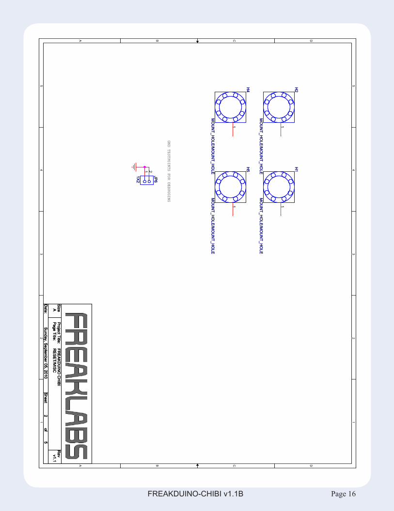
PCB LayoutPCB layout file order:
1. Mechanical Dimensions
2. Top Layer
3. Bottom Layer
4. Assembly Drawing - Silkscreen View
5. Assembly drawing - Reference Designator View

Page 18FREAKDUINO-CHIBI v1.1B
Page 19FREAKDUINO-CHIBI v1.1B
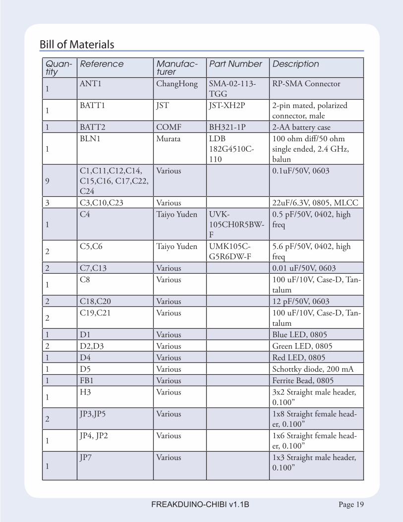
Bill of Materials
Quan-tity
Reference Manufac-turer
Part Number Description
1 ANT1 ChangHong SMA-02-113-TGG
RP-SMA Connector
1 BATT1 JST JST-XH2P 2-pin mated, polarized connector, male
1 BATT2 COMF BH321-1P 2-AA battery case
1BLN1 Murata LDB
182G4510C- 110
100 ohm diff/50 ohm single ended, 2.4 GHz, balun
9C1,C11,C12,C14, C15,C16, C17,C22, C24
Various 0.1uF/50V, 0603
3 C3,C10,C23 Various 22uF/6.3V, 0805, MLCC
1C4 Taiyo Yuden UVK-
105CH0R5BW-F
0.5 pF/50V, 0402, high freq
2 C5,C6 Taiyo Yuden UMK105C-G5R6DW-F
5.6 pF/50V, 0402, high freq
2 C7,C13 Various 0.01 uF/50V, 0603
1 C8 Various 100 uF/10V, Case-D, Tan-talum
2 C18,C20 Various 12 pF/50V, 0603
2 C19,C21 Various 100 uF/10V, Case-D, Tan-talum
1 D1 Various Blue LED, 08052 D2,D3 Various Green LED, 08051 D4 Various Red LED, 08051 D5 Various Schottky diode, 200 mA1 FB1 Various Ferrite Bead, 0805
1 H3 Various 3x2 Straight male header, 0.100”
2 JP3,JP5 Various 1x8 Straight female head-er, 0.100”
1 JP4, JP2 Various 1x6 Straight female head-er, 0.100”
1JP7 Various 1x3 Straight male header,
0.100”

Page 20FREAKDUINO-CHIBI v1.1B
Quan-tity
Reference Manufac-turer
Part Number Description
1 J1 4UCON 09558 USB Mini-AB connector
1 J2 4UCON 05537 DC Power Jack, 2.0 mm center conductor
1 L1 Abracon ATFC-0402-3N0-BT
3.0 nH, 0402, high freq
2 L2,L3 Various 47 uH inductor, 200 mA
2 Q1,Q2 Diodes, Inc 2N7002 N-channel enhancement FET
4 R1,R7,R8,R10 Various 330 ohms, 0805
14R2, R6, R9, R11, R13, R16, R17, R20, R21, R24, R25
Various 10 kohms, 0603
3 R12, R14, R18 Various 15 kohms, 08052 R3,R23 Various 47 kohms, 06032 R4,R5 Various 1 kohms, 06031 SW1 Various 2-input DIP switch1 S1 See-Plus SK-12D01-VG2 Right angle slide switch
1 S2 Various SMD SPST Tactile Switch/Pushbutton
1 U1 FTDI FT232RL USB to Serial Converter1 U2 Atmel AT86RF230 2.4 GHz, 802.15.4 radio1 U3 Holtek HT7750A 5V Boost Converter1 U4 Atmel ATMEGA328P AVR Microcontroller1 VR1 NJRC NJM2391-3.3 3.3V Regulator1 VR2 NJRC NJM2391- 5.0 5.0V Regulator1 Y1 NDK NX3225SA 16 MHz crystal, 15 ppm


