
ENGINEERING PHYSICS MATERIAL
GOKARAJU RANGARAJUINSTITUTE OF
ENGINEERING AND TECHNOLOGY
(Autonomous)
Bachupally, Hyderabad – 500 090
Engineering Physics I B. Tech CE/ME
GRIET Page 2
Preface
The main objective of the material entitled “Engineering Physics” is to make the I B. Tech
(CE, ME) students familiar with the basic concepts of physics in a more systematic manner.
This material is written according to GRIET (Autonomous) syllabus .This book has been
prepared to meet the requirements of Engineering Physics course as per new AICTE
Regulations.
This book is written and verified by the faculty of Department of Physics.
Dr. G. Patrick, Professor
Dr. M. Sridhar, Professor
Dr. K. Vagdevi, Associate professor
Dr. J. Kishore Babu, Assistant Professor
Mr. M. Krishna, Assistant Professor
Ms. B. Shanti Sree, Assistant Professor
Ms. G. Kalpana, Assistant Professor

Engineering Physics I B. Tech CE/ME
GRIET Page 3
Gokaraju Rangaraju Institute of Engineering& Technology
(Autonomous)
GR20A1004: Engineering Physics
(Common to CE and ME)
Syllabus
B. Tech I Year L: 3 T: 1 P: 0 C: 4
Course Objectives:
• Explain the interaction of light with matter through interference and diffraction
phenomena.
• Discuss the use of lasers as light sources in optical fiber applications.
• Outline the behavior of free electrons in materials.
• Describe the properties and fabrication methods of nanomaterials.
• Recognize the basic concepts of acoustics and ultrasonic.
Course Outcomes:
• Apply the principles of interference and diffraction of light in engineering applications.
• Analyze the properties of Laser and its propagation in different types of optical fibers.
• Classify materials based on the theory of Kronig Penny model.
• Enumerate the nature and characterization of nanomaterials and its applications.
• Use the concepts of acoustics and non-destructive testing in solving engineering
problems.
UNIT I
Wave Optics: Superposition of waves and interference of light by wave front splitting and
amplitude splitting, Young’s double slit experiment, Interference in thin films by reflection,
Newton’s rings, Difference between interference and diffraction, Fraunhofer diffraction from a
single slit, Diffraction grating, Grating spectrum and resolving power, Determination of
wavelength of light using diffraction grating.
UNIT II
Lasers: Interaction of radiation with matter: Absorption, Spontaneous emission and Stimulated
emission, Characteristics of lasers, Einstein coefficients, Resonating cavity, Active medium-
Meta stable state, Pumping, Population inversion, Construction and working of Ruby laser and
He-Ne laser, Applications of lasers.

Engineering Physics I B. Tech CE/ME
GRIET Page 4
Fiber Optics: Introduction, Principle and Structure of an optical fiber, Basic components in
optical fiber communication system, Comparison of optical fibers over conventional cables,
Acceptance angle-Numerical aperture, Types of fibers, Losses associated with optical fibers,
Applications of optical fibers.
UNIT III
Introduction to solids: Fermi Energy level, Fermi distribution function, Bloch’s theorem,
Kronig – Penny model (Qualitative), E-K diagram, Brillouin Zones, Effective mass of electron,
Origin of energy bands, Classification of materials on the basis of energy bands, Intrinsic and
extrinsic semiconductors (Qualitative), Direct and Indirect band gap semiconductors.
UNIT IV
Engineered semiconductor materials: Nanomaterials, Introduction, Quantum confinement,
Surface to volume ratio, Classification of nanomaterials as 0D, 1D, 2D and 3D (qualitative),
Examples of low-dimensional systems such as quantum wells, wires and dots, Fabrication: Top-
Down technique by CVD method, Bottom–Up technique by Sol-Gel method, Characterization
techniques: SEM, TEM and EDAX.
UNIT V
Acoustics: Basic requirements of acoustically good hall, Reverberation and Reverberation time,
Sabine’s formula for Reverberation time (Qualitative), Measurement of absorption coefficient of
a material, Factors affecting the architectural acoustics and their remedies.
Ultrasonics: Introduction, Classification of ultrasonic waves: Longitudinal waves, Transverse
waves, Surface waves and Plate waves, Production of ultrasonic waves: Piezoelectric method
and Magnetostriction method, Properties of ultrasonic waves, Applications of ultrasonics:
SONAR and NDT (Pulse echo method).
Teaching methodologies:
• White board and marker
• Power Point Presentations
• Video lectures
Text Books:
1. Engineering Mechanics, 2nd ed.- MK Harbola, Cengage Learning
2. Mechanics, D S Mathur and P S Hemne, S Chand
3. I. G. Main, “Vibrations and waves in physics’, 3rd Edn, Cambridge University Press, 2018
4. Applied Physics, T. Bhīma Sankaram, BSP Publishers.
5. Engineering Physics, P.K Palanisamy, Scitech Publishers.
6. AjoyGhatak, “Optics”, McGraw Hill Education, 2012
References:
1. H. J. Pain, “The physics of vibrations and waves”, Wiley, 2006
2. O. Svelto, “Principles of Lasers”
3. “Introduction to Mechanics”, M.K.Verma, Universities Press
Engineering Physics I B. Tech CE/ME
GRIET Page 5
UNIT –I
WAVE OPTICS
INTERFERENCE
Introduction: Light means the saffron sunrise, the rainbow, the blue sky, the red sunset, the
pleasant moon, the eclipse and many more treasures of visual pleasures to us.
Principle of superposition: states that ,the net displacement of given point in space at any time
due to two or more waves is the algebraic sum of the displacements produced at that point by all
waves.
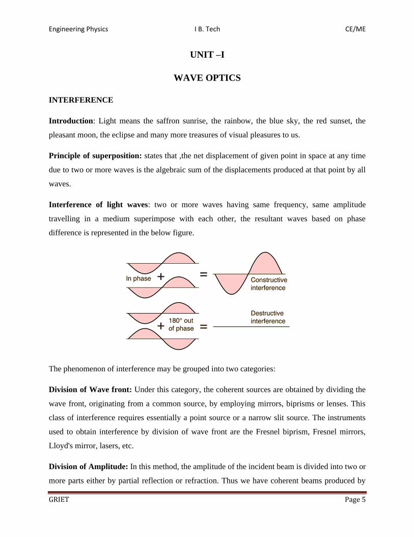
Interference of light waves: two or more waves having same frequency, same amplitude
travelling in a medium superimpose with each other, the resultant waves based on phase
difference is represented in the below figure.
The phenomenon of interference may be grouped into two categories:
Division of Wave front: Under this category, the coherent sources are obtained by dividing the
wave front, originating from a common source, by employing mirrors, biprisms or lenses. This
class of interference requires essentially a point source or a narrow slit source. The instruments
used to obtain interference by division of wave front are the Fresnel biprism, Fresnel mirrors,
Lloyd's mirror, lasers, etc.
Division of Amplitude: In this method, the amplitude of the incident beam is divided into two or
more parts either by partial reflection or refraction. Thus we have coherent beams produced by

Engineering Physics I B. Tech CE/ME
GRIET Page 6
division of amplitude. These beams travel different paths and are finally brought together to
produce interference. The effects resulting from the superposition of two beams are referred to as
two beam interference and those resulting from superposition of more than two beams are
referred to as multiple beam interference. The interference in thin films, Newton's rings, and
Michelson's interferometer are examples of two beam interference and Fabry-Perot's
interferometer is an example of multiple beam interference.
Theory of interference:
From fig, points A, B are the two sources which produce waves of equal amplitude and constant
phase difference.Points shown by circles will have minimum displacement as crest of one wave
falls on the trough of another and the resultant displacement is zero.Points shown by crosses in
the diagram will have maximum displacement as either crest of one wave will combine with the
other.
As the intensity (energy) is directly proportional to square of amplitude (I ∞ A2) the intensity at
these points is four times the intensity due to one wave.There is no loss of energy due to
interference. The energy is transferred from the points of minimum displacement to the points of
maximum displacement.
Experimental setup: Young’s allowed the sunlight to fall on a pinhole ‘S’ and then at some
distance away on two pinholes A, B.A, B are equidistant from ‘S and are close to each other.
Spherical waves spread out form ‘S’ .also spread out from ‘A’ and ‘B’. These waves are of same

Engineering Physics I B. Tech CE/ME
GRIET Page 7
amplitude and wavelength, interference bands are produced which are alternatively dark and
bright on the screen.Points ‘E’ are bright as the crest due to one wave coincides with crest due to
other and they reinforce with each other.Points ‘F’ are dark, as the crest of one falls on the trough
of the other and they neutralize the effect of each other. Points similar to ‘E’ are also bright as
trough of one falls on trough of the other.
Analytical treatment of interference:
Consider a monochromatic source of light ‘S’ emitting waves of wavelength ‘ λ‘ and passed
through two narrow pinholes ‘A’ and ‘B’.‘A’, ‘B’ are equidistant from ‘S’ and act as two virtual
coherent sources.
a = amplitude of waves,
δ = phase difference of two waves reaching at point ‘P’
If Y1 and Y2 are the displacements
𝑦1 = 𝑎 sin 𝜔𝑡
𝑦2 = 𝑎 sin(𝜔𝑡 + 𝛿)
So 𝑌 = 𝑦1 + 𝑦2 = 𝑎 sin 𝜔𝑡 + 𝑎 sin(𝜔𝑡 + 𝛿)
𝑌 = 𝑎 sin 𝜔𝑡 + 𝑎 sin 𝑐𝑜𝑠 𝛿 + 𝑎 𝑐𝑜𝑠 𝜔𝑡 sin 𝛿
𝑌 = 𝑎 sin 𝜔𝑡 ( 1 + cos 𝛿) + 𝑎 𝑐𝑜𝑠 𝜔𝑡 sin 𝛿…… (1)
If 𝑎( 1 + cos 𝛿) = 𝐴 cos 𝜃, 𝑎 sin 𝛿 = 𝐴 sin 𝜃 … . (2)𝑖𝑛 (1)
𝑌 = 𝐴 sin 𝜔𝑡 cos 𝜃 + 𝐴 cos 𝜔𝑡 sin 𝜃
𝑌 = 𝐴 sin(𝜔𝑡 + 𝜃) … . (3)
Represents the equation of simple harmonic vibration of amplitude ‘A’ .
Squaring and adding eqn (2)
𝐴2𝑠𝑖𝑛2𝜃 + 𝐴2𝑐𝑜𝑠2𝜃 = 𝑎2𝑠𝑖𝑛2𝛿 + 𝑎2(1 + cos 𝛿)2

Engineering Physics I B. Tech CE/ME
GRIET Page 8
𝐴2(𝑠𝑖𝑛2𝜃 + 𝑐𝑜𝑠2𝜃) = 𝑎2𝑠𝑖𝑛2𝛿 + 𝑎2(1 + 𝑐𝑜𝑠2 𝛿 + 2 cos 𝛿)
𝐴2 = 𝑎2𝑠𝑖𝑛2𝛿 + 𝑎2 + 𝑎2𝑐𝑜𝑠2 𝛿 + 2 𝑎2 cos 𝛿)
𝐴2 = 2𝑎2 + 2 𝑎2 cos 𝛿)
𝐴2 = 2𝑎2(1 + cos 𝛿)
𝐴2 = 2𝑎22𝑐𝑜𝑠2𝛿
2
𝐴2 = 4 𝑎2𝑐𝑜𝑠2𝛿
2
Intensity at a point is given by the square of the amplitude
𝐼 = 𝐴2
𝐼 = 4 𝑎2𝑐𝑜𝑠2𝛿
2
Special cases:
Case I: when phase difference δ = 0, 2π, 3π, 4π…2n π or path difference = x = 0, λ, 2λ,….nλ
𝐼 = 4 𝑎2𝑐𝑜𝑠2(0)
𝐼 = 4 𝑎2
i.e intensity is maximum when the phase difference is a whole number of multiple of 2π or path
difference is a whole number multiple of wavelength.
Case II: When phase difference, δ = π, 3π… (2n+1)π or path difference
x= 𝜆
2,
3𝜆
2,
5𝜆
2, … . . (2𝑛 + 1)
𝜆
2
𝐼 = 4 𝑎2𝑐𝑜𝑠2(𝜋)
𝐼 = 0
Intensity is minimum, when the path difference is an odd number multiple of half wave length

Engineering Physics I B. Tech CE/ME
GRIET Page 9
Young’s double slit experiment :( interference due to division of wave front)
The phenomenon of interference of light has proved the validity of wave theory of light.
In 1802, Thomas Young experimented on interference of light.
Consider a narrow monochromatic source ‘S’ and two pinholes ‘A’ and ‘B’,equidistant from
‘S’.‘A’ and ‘B’ act as two coherent sources separated by a distance‘d’. Let a screen be placed at
a distance ‘D’ from the coherent source. The point ‘C’ on the screen is equidistant from ‘A’ and
‘B’ and as the path difference between the two waves is zero, the point ‘C’ has maximum
intensity.
Consider a point ‘P’ at a distance ‘x’ from ‘C’. The waves from ‘A’ and ‘B’ reach at the point
‘P’ on the screen.
Here, = 𝑋 −𝑑
2 , 𝑃𝑅 = 𝑋 +
𝑑
2
(𝐵𝑃)2 − (𝐴𝑃)2 = [𝐷2 + (𝑋 +𝑑
2)2] − [ 𝐷2 + (𝑋 −
𝑑
2)2]
(𝐵𝑃)2 − (𝐴𝑃)2 = 2𝑥𝑑
𝐵𝑃 − 𝐴𝑃 =2𝑥𝑑
𝐵𝑃 + 𝐴𝑃
But 𝐵𝑃 = 𝐴𝑃 ≃ 𝐷
Therefore path difference = 𝐵𝑃 − 𝐴𝑃 =2𝑋𝑑
2𝐷=
𝑥𝑑
𝐷

Engineering Physics I B. Tech CE/ME
GRIET Page 10
Phase difference = 2𝜋
𝜆(
𝑥𝑑
𝐷)
Bright fringes: if the path difference is a whole number of multiples of wavelength ‘λ’, the point
‘P’ is bright as
𝑥𝑑
𝐷= 𝑛𝜆, 𝑤ℎ𝑒𝑟𝑒 𝑛 = 0,1,2,3, ..
So ,𝑛𝜆𝐷
𝑑= 𝑥 , gives the distance of the bright fringes from the point ‘C’. At ‘C’, the path
difference is zero and a bright fringe is formed.
When 𝑛 = 1, 𝑥1 = 𝜆𝐷
𝑑
𝑛 = 2, 𝑥2 = 2𝜆𝐷
𝑑
𝑛 = 3, 𝑥3 = 3𝜆𝐷
𝑑
𝑥𝑛 = 𝑛𝜆𝐷
𝑑
The distance between any to consecutive bright fringes is
𝑥2 − 𝑥1 =2𝜆𝐷
𝑑−
𝜆𝐷
𝑑=
𝜆𝐷
𝑑… (1)
Dark fringes:If the path difference is an odd number multiple of half wavelength, the point ‘P’
is dark.
𝜆𝑑
𝐷= (2𝑛 + 1)
𝜆
2, 𝑤ℎ𝑒𝑟𝑒 𝑛 = 0,1,2, …
Or 𝑥 =(2𝑛+1)𝜆𝐷
2𝑑 gives the distance of dark fringes from the point ‘C’
When 𝑛 = 1, 𝑥1 = 3𝜆𝐷
2𝑑
𝑛 = 2, 𝑥2 = 5𝜆𝐷
2𝑑

Engineering Physics I B. Tech CE/ME
GRIET Page 11
𝑥𝑛 = (2𝑛 + 1)𝜆𝐷
2𝑑
The distance between any two consecutive dark fringes is
𝑥2 − 𝑥1 = 5𝜆𝐷
2𝑑−
3𝜆𝐷
2𝑑=
𝜆𝐷
𝑑..(2)
The distance between any two consecutive bright or dark fringes is known as fringe width.
Bright and dark fringes are formed alternatively on both sides of ‘C’.From equations (1),(2), the
width of the bright fringe is equal to the width of the dark fringe. All the fringes are equal in
width and are independent of the order of the fringe.The breadth of a bright or dark fringe is
equal to half the fringe width ad is equal to𝜆𝐷
2𝑑. The fringe width is 𝛽 =
𝜆𝐷
𝑑
Energy distribution: from 𝐼 = 4 𝑎2𝑐𝑜𝑠2 𝛿
2, it is found that the intensity at bright points = 4 𝑎2,
and at dark points it is zero.According to the law of conservation of energy, the energy cannot be
destroyed, here also, the energy is not destroyed, but only transferred from the points of
minimum intensity to the points of maximum intensity. Therefore the formation of interference
fringes is in accordance with the law of conservation of energy.
Interference in thin films: (Division of amplitude) Newton and Hooke observed and
developed the interference phenomenon due to multiple reflections from the surface of thin
transparent materials.
Engineering Physics I B. Tech CE/ME
GRIET Page 12
Ex: familiar with beautiful colors produced by the thin film of oil on the surface of water and
also by the thin film of a soap bubble. Hooke also observes such colors in thin films of mica.
Newton was able to show the inference rings when a convex lens was placed on a glass plate.
Young was able to explain the phenomenon on the basis of interference between light reflected
from the top and the bottom surface of a thin film. It has been observed that, interference in the
case of thin films take s place due to (1) reflected light and (2) transmitted light.
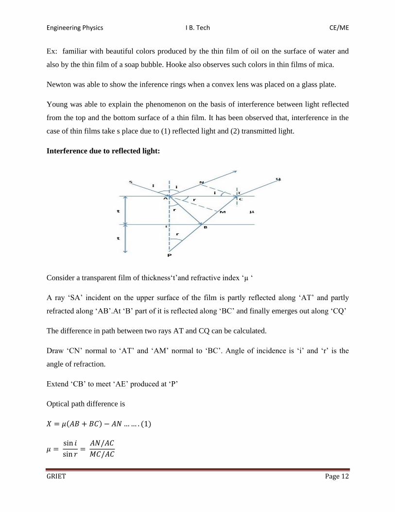
Interference due to reflected light:
Consider a transparent film of thickness‘t’and refractive index ‘µ ‘
A ray ‘SA’ incident on the upper surface of the film is partly reflected along ‘AT’ and partly
refracted along ‘AB’.At ‘B’ part of it is reflected along ‘BC’ and finally emerges out along ‘CQ’
The difference in path between two rays AT and CQ can be calculated.
Draw ‘CN’ normal to ‘AT’ and ‘AM’ normal to ‘BC’. Angle of incidence is ‘i’ and ‘r’ is the
angle of refraction.
Extend ‘CB’ to meet ‘AE’ produced at ‘P’
Optical path difference is
𝑋 = 𝜇(𝐴𝐵 + 𝐵𝐶) − 𝐴𝑁 … … . (1)
𝜇 = sin 𝑖
sin 𝑟=
𝐴𝑁/𝐴𝐶
𝑀𝐶/𝐴𝐶
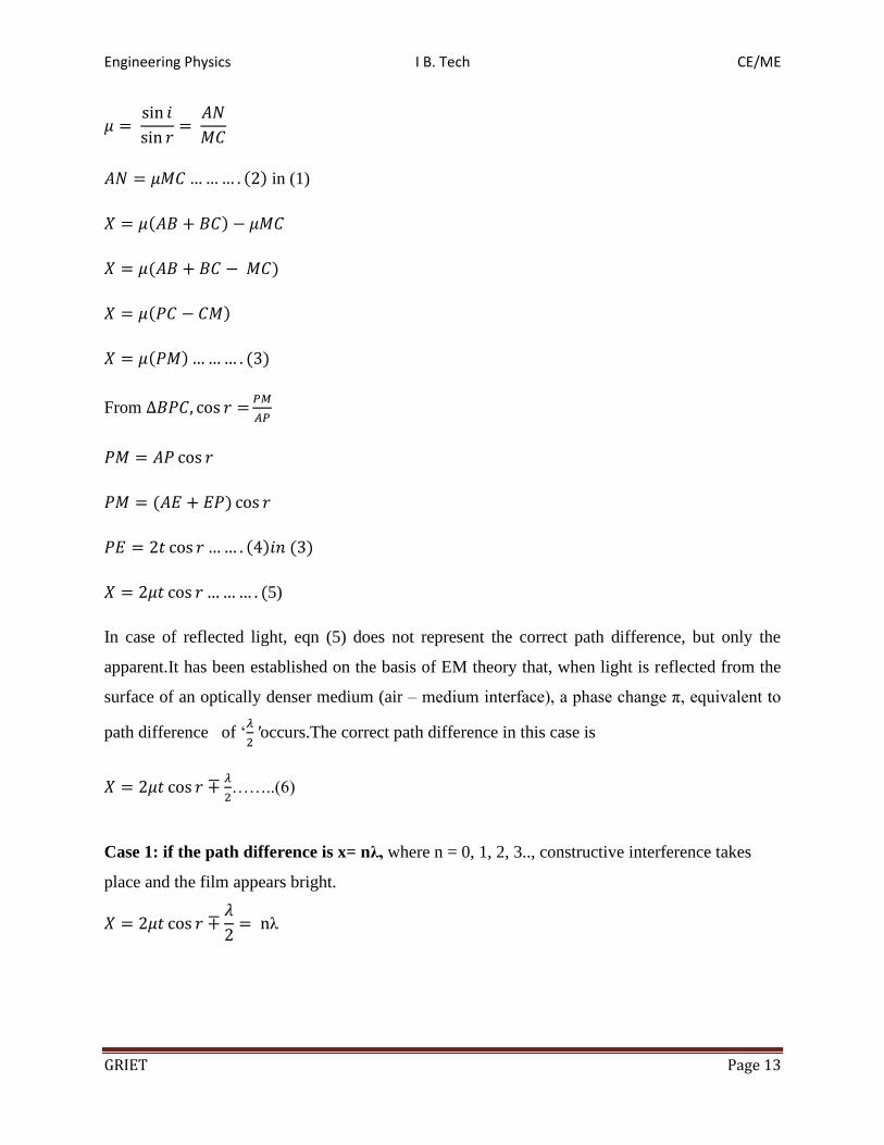
Engineering Physics I B. Tech CE/ME
GRIET Page 13
𝜇 = sin 𝑖
sin 𝑟=
𝐴𝑁
𝑀𝐶
𝐴𝑁 = 𝜇𝑀𝐶 … … … . (2) in (1)
𝑋 = 𝜇(𝐴𝐵 + 𝐵𝐶) − 𝜇𝑀𝐶
𝑋 = 𝜇(𝐴𝐵 + 𝐵𝐶 − 𝑀𝐶)
𝑋 = 𝜇(𝑃𝐶 − 𝐶𝑀)
𝑋 = 𝜇(𝑃𝑀) … … … . (3)
From ∆𝐵𝑃𝐶, cos 𝑟 =𝑃𝑀
𝐴𝑃
𝑃𝑀 = 𝐴𝑃 cos 𝑟
𝑃𝑀 = (𝐴𝐸 + 𝐸𝑃) cos 𝑟
𝑃𝐸 = 2𝑡 cos 𝑟 … … . (4)𝑖𝑛 (3)
𝑋 = 2𝜇𝑡 cos 𝑟 … … … . (5)
In case of reflected light, eqn (5) does not represent the correct path difference, but only the
apparent.It has been established on the basis of EM theory that, when light is reflected from the
surface of an optically denser medium (air – medium interface), a phase change π, equivalent to
path difference of ‘𝜆
2′occurs.The correct path difference in this case is
𝑋 = 2𝜇𝑡 cos 𝑟 ∓𝜆
2……..(6)
Case 1: if the path difference is x= nλ, where n = 0, 1, 2, 3.., constructive interference takes
place and the film appears bright.
𝑋 = 2𝜇𝑡 cos 𝑟 ∓𝜆
2= nλ
Engineering Physics I B. Tech CE/ME
GRIET Page 14
𝑋 = 2𝜇𝑡 cos 𝑟 = (2𝑛 ∓𝜆
2)…… (7)
Case 2: if the path difference is x = (2𝑛 + 1)𝜆
2, where n= 0,1,2,3.. Destructive interference
takes place and the film appears dark.
𝑋 = 2𝜇𝑡 cos 𝑟 ∓𝜆
2= (2𝑛 + 1)
𝜆
2
2𝜇𝑡 cos 𝑟 = (𝑛 + 1)λ
Here n is an integer only; so (n+1) can be taken as ‘n’2𝜇𝑡 cos 𝑟 = 𝑛λ
It should be remembered that, the interference pattern will not be perfect .Therefore, the rays
‘AT’ and ‘CQ’ will not be the same and their amplitude is different. The amplitudes will depend
on the amount of light reflected and transmitted through the films.
For normal incidence, about 4% of incident light is reflected and 96% is transmitted. There is a
small difference in amplitude of rays ‘BQ’ and ‘DR’ and the intensity never vanishes completely
and perfect dark fringes will not be observed for the rays ‘BQ’ and ‘DR’ alone.
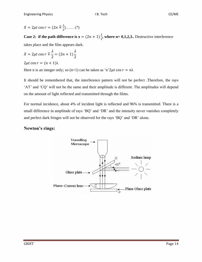
Newton’s rings:

Engineering Physics I B. Tech CE/ME
GRIET Page 15
When a Plano convex lens of long focal length is placed on a plane glass plate, a thin air film is
enclosed between the lower surface of the lens and the upper surface of the plate.The thickness
of the air film is very small at the point of contact and gradually increases from the center
outwards.Fringes produce with monochromatic light are circular fringes are concentric circles,
uniform in thickness with the center of point of contact. When viewed with white light, fringes
are colored. With monochromatic light, bright and dark circular fringes are produced in the air
film.From fig: S= source of monochromatic light at the focus of lens ‘c’Horizontal beam of light
falls on the glass plate ‘G’ at 45ο.Glass plate ‘P’ reflects a part of the incident light towards the
air film enclosed by the lens ‘C’ and plane glass plate ‘P’. Reflected beam form the air film is
viewed with a microscope ‘M’.Interference takes place, dark and bright circular fringes are
produced.This is due to the interference between the light reflected from the lower surface of the
lens and upper surface of the glass plate ‘G’.
Newton’s rings by reflected light:
R= radius of curvature of the lens, t = thickens of the air film at a distance of OQ=r, from point
of contact ‘O’

Engineering Physics I B. Tech CE/ME
GRIET Page 16
To find the thickness of the air film:
According to the theory of intersection of chords, from the above figure,
𝐻𝑃 = 𝑀𝑂
𝐻𝐸 × 𝐸𝑃 = 𝑀𝐸 × 𝐸𝑂
𝑟 × 𝑟 = (𝑀𝐶 + 𝐶𝑂 − 𝐸𝑂) 𝐸𝑂
𝑟2 = (𝑅 + 𝑅 − 𝑡) 𝑡
𝑟2 = (2𝑅 − 𝑡) 𝑡… (1)
As 𝑅 ≫ 𝑡, 2𝑅 − 𝑡 = 𝑡 in (1)
𝑟2 = 2𝑅 𝑡
𝑡 =𝑟2
2𝑅….. (2)
To find the diameter of the rings and wavelength of the source:
For dark rings: We know that 2𝜇𝑡 cos 𝑟 = 𝑛λ … (3)
As 𝜇 = 1 forair and as ‘r’ is small, cos r=1 in (3)
2𝑡 = 𝑛λ … (4)
Substitute (2) in (4)
2𝑟2
2𝑅= 𝑛λ
𝑟2 = 𝑛λR
𝑟 = √𝑛λR
Diameter =D=2r
𝐷𝑛 = 2𝑟 = 2√𝑛λR

Engineering Physics I B. Tech CE/ME
GRIET Page 17
𝐷𝑛2 = 4 𝑛λR
𝐷𝑛+𝑚2 = 4 (𝑛 + 𝑚)λR
𝐷𝑛+𝑚2 − 𝐷𝑛
2 = 4 (𝑛 + 𝑚)λR − 4 𝑛λR
= 4λR (n + m − n)
𝐷𝑛+𝑚2 − 𝐷𝑛
2 = 4λRm
Wavelength is 𝜆 =𝐷𝑛+𝑚
2 − 𝐷𝑛2
4 Rm, Similarly for bright fringes we get, 𝜆 =
𝐷𝑛+𝑚2 − 𝐷𝑛
2
4 Rm
Therefore fringe width decreases with the order of the fringe and the fringes get closer with
increase in their order.The radius of curvature of lower surface of the lens is determined with the
help of a spherometer, but more accurately it is determined by Boy’s method. Hence the
wavelength of a given monochromatic source of light can be determined.
Newton’s rings with white light: with monochromatic light, Newton’s rings are alternatively
dark and bright. The diameter of the ring depends upon the wavelength of light used. When
white light is used, the diameter of the rings of different colors will be different and colored rings
are observed.Only the first few rings are clear and after that due to overlapping of the rings of
different colors, the rings can’t be viewed.
DIFFRACTTION:
The bending of light round the edges of an obstacle or the encroachment of light within the
geometrical shadow is called diffraction.

Engineering Physics I B. Tech CE/ME
GRIET Page 18
When a beam of light passes through a small opening (a small circular hole or a narrow slit), it
spreads to some extent into the region of geometrical shadow. If light energy is propagated in the
form of waves, similar to sound waves, bending of light round the edges of an opaque obstacle or
illumination of the geometrical shadow is expected. When waves encounter obstacles, they bend
round the edges of the obstacles; if the dimensions of the obstacles are comparable to the
wavelength of the waves diffraction pattern can be captured.
According to Huygens’ theory, each progressive wave produces secondary waves and the
envelope forms the secondary wave front
Fig sows the passage of waves through an opening, when opening is large compared to a
wavelength, the waves do not bend round the edges, when the opening is small the bending
effect round the edges is noticeable. When opening is small, the waves spread overall the surface
behind the opening. The opening acts as an independent source of waves, which propagate in all
directions behind the opening.

Engineering Physics I B. Tech CE/ME
GRIET Page 19
When slit is very small, diffraction effect is observable quite close to slit.When slit is large,
diffraction is observed at greater distances from the opening.
Thus, larger the obstacle, greater the distance at which diffraction is detected provided when
waves have enough energy.Diffraction effect will be observed only when a narrow source is used
and a part of the wave is cut off by some obstacle.
Note: diffraction of light is the result of superimposition of waves from coherent sources on the
same wavefront after the wavefront has been distorted by some obstacles.
Types of diffraction: based on the wavelength of the source, size of the obstacle and the
distance between the source and the screen, there are two types of diffractions.
(1) Fresnel diffraction (2) Fraunhoffer diffraction.
Fresnel diffraction: In which either the point source or the screen or both are at finite distances
from the obstacle.Deals with non plane wave fronts,experimentally simple, but the analysis is
complex.
Fraunhoffer diffraction: Source and screen are at infinite distance from obstacles,deals with
parallel rays and plane wave fronts. Conditions required for this diffraction are easily achieved
using lenses. Can be established in the laboratory on a spectrometer. Simple to analyze
mathematically.

Engineering Physics I B. Tech CE/ME
GRIET Page 20
Note: As the rays are parallel and in view of its simplicity, we restrict our study to Fraunhoffer
diffraction only.
Fraunhoffer diffraction at a single slit:
In Fraunhoffer diffraction, the source is at infinite distance, a collimated parallel beam of
monochromatic light of wavelength ‘λ’ is incident normally on a narrow slit AB of width ‘a’ as
shown in fig.
According to Hugens Principle, We divide this wavefront into a large number of points ‘n’ each
sending waves of equal amplitude ‘a’. These waves get diffracted and then interfere to produce
diffraction pattern on the screen. The secondary waves that travel along the direction of incident
beam are focused at point ‘P1’while those inclined at an angle ‘θ’ with the direction of incident
beam (due to diffraction) are focused at another point ‘P2’.
To find the resultant intensity at point p1,we draw a perpendicular AN on BN.it is clear from the
figure that the optical paths of the waves traveled after the plane AN to the point P1 are equal.
However, the optical paths of the waves originating from points on AB (from A towards B) and
reaching the point P1 gradually increase. Hence, the phase difference between them gets larger.
This is shown in fig.
For n number of waves each of amplitude ‘a’. In this figure a phase difference of ϕ is taken
between two successive waves. The resultant amplitude of these waves at point ‘P1’ is shown as
‘R,

Engineering Physics I B. Tech CE/ME
GRIET Page 21
the total path difference between the waves originating from extreme point s A and B is 𝐴𝑁 =
𝐴𝐵𝑆𝑖𝑛 𝜃 = 𝑎 𝑠𝑖𝑛𝜃.ther fore the path difference between different waves originating from all the
points of the slit AB vary between zero and 𝑎 𝑠𝑖𝑛𝜃.
The phase difference corresponding to path difference 𝑎 𝑠𝑖𝑛𝜃 will be2𝜋
𝜆 a sinθ . Since the
aperture is divided into n equal parts, the phase difference between any two consecutive parts
will be 1
𝑛
2𝜋
𝜆 a sinθ = (∅ say). The resultant amplitude and intensity at point P1 due to all the
secondary waves can be obtained by vector polygen method.
Let 𝛼 be the phase difference between the waves for the initial direction to the resultant, then 2𝛼
will be the total phase difference between the secondary waves originating from extreme
point s of the slit AB. Here it is taken that all the amplitudes constitute an arc due to their
large number and small phase difference between them. Because of the symmetry, we have
˪ 𝑂 = 𝛼 𝑎𝑛𝑑 ˪ 𝑄 = 2𝛼.the chord OP gives the resultant amplitude due to all the secondary
waves at point P1.
Then in the ∆𝑂𝐶𝑁
𝑆𝑖𝑛 𝛼 =𝑂𝑁
𝑂𝐶=
𝑂𝑁
𝑟… (1)
𝑂𝑁 = 𝑟 𝑆𝑖𝑛 𝛼
r = radius of the circular arc
𝐶ℎ𝑜𝑟𝑑 𝑂𝑃 = 2 𝑂𝑁 = 2 𝑟 sin 𝛼

Engineering Physics I B. Tech CE/ME
GRIET Page 22
𝐶ℎ𝑜𝑟𝑑 𝑂𝑃 = 𝑟𝑒𝑠𝑢𝑙𝑡𝑎𝑛𝑡 𝑎𝑚𝑝𝑙𝑖𝑡𝑢𝑑𝑒
𝑅 = 2 𝑟 sin 𝛼 … . (2)
The length of the arc = 𝑛𝑎 , where n is an integer and a= amplitude of each vibration.
We know that ˪ 𝑃𝐶𝑂 = 2 𝛼 =𝐴𝑟𝑐 𝑂𝑁𝐼𝑃
𝑅𝑎𝑑𝑖𝑢𝑠=
𝑛𝑎
𝑟
Or 2𝑟 =𝑛𝑎
𝛼… (3)
Substituting the value of 2r in eqn (2), we get
𝑅 = 𝑛𝑎 sin 𝛼
𝛼
𝑅 = 𝐴0
sin 𝛼
𝛼, 𝑤ℎ𝑒𝑟𝑒 𝑛𝑎 = 𝐴0
Thus the resultant intensity at a point P1 on the screen is given by a measure of
𝐼 = 𝑅2 = 𝐴02
𝑠𝑖𝑛𝛼2
𝛼2= 𝐼0 [
sin 𝛼
𝛼]
2
𝐼 = 𝐼0 [sin 𝛼
𝛼]
2
… (5)
Thus, the magnitude of the resultant intensity at any point on the screen is a function of 𝛼
and the slit width ′𝑎′. The phase difference of 2𝛼 is introduced due to the path difference of
𝑎 𝑠𝑖𝑛 𝜃 ,Therefore 2𝛼 = 2𝜋
𝜆 𝑎 sin 𝜃
Conditions of maxima and minima:
It is clear from eqn (4) that the resultant amplitude R will be a maximum when
sin 𝛼
𝛼= 1, 𝑤ℎ𝑖𝑐ℎ 𝑖𝑠 𝑡𝑟𝑢𝑒 𝑤ℎ𝑒𝑛 𝛼 → 0, 𝑖. 𝑒.
𝜋
𝜆𝑎 sin 𝜃 → 0 𝑜𝑟 sin 𝜃 → 0

Engineering Physics I B. Tech CE/ME
GRIET Page 23
𝜃 = 𝑜°, From eqn (4),
𝑅 =𝐴0
𝛼[𝛼 −
𝛼3
˪3−
𝛼5
˪5+
𝛼7
˪7+ ⋯ . . ]
𝑅 = 𝐴0 [1 −𝛼2
˪3−
𝛼4
˪5+
𝛼6
˪7+ ⋯ . . ]
𝑅 = 𝐴0 𝑓𝑜𝑟 𝛼 = 0, Hence the intensity corresponding to 𝛼 = 0 𝑖𝑠 𝐼 = 𝑅2 = 𝐴02 = 𝐼0.
This is called as the intensity of central (principal) maximum.
In order to determine the position of maximum intensity, let us differentiate eqn(5) w.e.to
𝛼 and equate it zero.
𝑑𝐼
𝑑𝛼= 2𝐼0
𝑆𝑖𝑛 𝛼
𝛼[𝛼 cos 𝛼 − sin 𝛼
𝛼2] = 0
Since 𝐼0 cannot be zero, either 𝑆𝑖𝑛 𝛼 = 0 𝑜𝑟 𝐶𝑜𝑠 𝛼 = 0. the equation 𝑆𝑖𝑛 𝛼 = 0 determines
the positions of minima (eqn (4)) except when 𝛼= 0, because it corresponds to the position
of maximum. Therefore, the following condition should be satisfied for obtaining the
minima.
𝑆𝑖𝑛 𝛼 = 0 𝑜𝑟 𝛼 = ∓ 𝑛𝜋
Or 𝜋
𝜆 𝑎 sin 𝜃 = ∓ 𝑛𝜋
𝑎 sin 𝜃 = ∓ 𝑛𝜋 , 𝑛 = 1,2,3, ..
The position of maxima is given by
𝛼 cos 𝛼 − 𝑆𝑖𝑛 𝛼 = 0, Or 𝛼 = tan 𝛼
This equation can be solved graphically by plotting the curves 𝑦 = 𝛼, 𝑎𝑛𝑑 𝑦 = tan 𝛼
The first relation𝑦 = tan 𝛼 represents the equation of straight line passing through the
origin making an angle of 450 with the axis and the equation 𝑦 = tan 𝛼 represents a
discontinuous curve having a number of branches with asymptotes at the intervals of 𝜋.
Engineering Physics I B. Tech CE/ME
GRIET Page 24
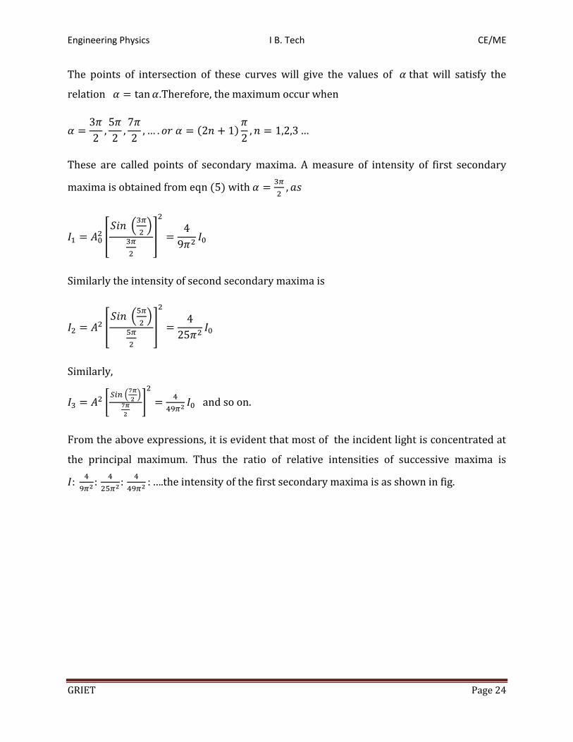
The points of intersection of these curves will give the values of 𝛼 that will satisfy the
relation 𝛼 = tan 𝛼.Therefore, the maximum occur when
𝛼 =3𝜋
2,5𝜋
2,7𝜋
2, … . 𝑜𝑟 𝛼 = (2𝑛 + 1)
𝜋
2, 𝑛 = 1,2,3 …
These are called points of secondary maxima. A measure of intensity of first secondary
maxima is obtained from eqn (5) with 𝛼 =3𝜋
2, 𝑎𝑠
𝐼1 = 𝐴02 [
𝑆𝑖𝑛 (3𝜋
2)
3𝜋
2
]
2
=4
9𝜋2𝐼0
Similarly the intensity of second secondary maxima is
𝐼2 = 𝐴2 [𝑆𝑖𝑛 (
5𝜋
2)
5𝜋
2
]
2
=4
25𝜋2𝐼0
Similarly,
𝐼3 = 𝐴2 [𝑆𝑖𝑛 (
7𝜋
2)
7𝜋
2
]
2
=4
49𝜋2 𝐼0 and so on.
From the above expressions, it is evident that most of the incident light is concentrated at
the principal maximum. Thus the ratio of relative intensities of successive maxima is
𝐼: 4
9𝜋2 : 4
25𝜋2 : 4
49𝜋2 : ….the intensity of the first secondary maxima is as shown in fig.

Engineering Physics I B. Tech CE/ME
GRIET Page 25
Width of central maximum:
Expression for minima in single slit diffraction is a sin𝜃 = ± 𝑚𝜆
For the first minima m=1, a sin𝜃 = 1𝜆

Engineering Physics I B. Tech CE/ME
GRIET Page 26
a sin𝜃 = 𝜆sin𝜃 = 𝜆
𝑎 … (1)
Let the distance of the first secondary minimum (P2) from the center of the principal maximum
(P1) be x from above figure
width of central maximum = 2x
If the lens L2 is very near, the slit or the screen is far away from the lens L2,then
𝑠𝑖𝑛𝜃 =𝑥
𝑓… (2)
f= focal length of the lens L2
from 1 & 2
𝜆
𝑎=
𝑥
𝑓
𝑥 =𝜆𝑓
𝑎… (3)
Therefore, the width of the central maximum W = 2𝑥
𝑊 =2𝜆𝑓
𝑎… (4)
Effect of slit Width, changing wave length:
From eqn 1 we can conclude that,
If slit width a is large, then for a given wavelength of light, 𝑠𝑖𝑛𝜃 is small and hence 𝜃 is small.
This means that the, maxima and minima lie very close to the central maximum
If slit width a is narrow, 𝜃 is large and then diffraction maxima and minima are quite distinct and
clear changing wave length:From eqn 3 we can conclude x∝ 𝜆 i.e., on increasing 𝜆 , x also
increases which means, the envelop becomes broader and the fringes move further apart.
Width of central maxima dependency:

Engineering Physics I B. Tech CE/ME
GRIET Page 27
From eqn 4 we can conclude that;The width of the central maximum is proportional to ‘λ’
(wavelength of the light).With red light (longer wave length), the width of the central maximum
is more than with violet light (shorter wavelength).With a narrow slit, the width of the central
maximum is more
Difference between Interference and diffraction:
It is clear from the double slit diffraction pattern that interference takes place between the
secondary waves originating from the corresponding points of the two slits and also that the
intensity of the interference maxima and minima is controlled by the amount of light reaching
the screen sue diffraction at the individual slits.
The resultant intensity at any point on the screen is obtained by multiplying the intensity function
for the interference and the intensity function for the diffraction at the two slits.
The values of the intensity functions are taken for the same direction of the secondary waves.
But the interference of all the secondary waves originating from the whole wavefront is termed
as diffraction. Once the pattern obtained on the screen may be called an interference pattern or a
diffraction pattern.
Note: interference- resultant amplitude at a point is obtained by superimposing of two or more
beams.
Diffraction can be defined as the phenomenon in which the resultant amplitude ata pint on the
screen is obtained by integrating the effect of infinitesimally small number of elements into
which the whole wave front can be divided. Thus, the resultant diffraction pattern obtained with
soluble slit can be taken as a combination of the effect of both interference and diffraction.
Diffraction Grating
Plane diffraction grating:
A diffraction grating is an extremely useful device and in one of its forms, it consists of a very
large number of narrow slits side by side, slits are separated by opaque spaces. There are two
types of gratings.

Engineering Physics I B. Tech CE/ME
GRIET Page 28
Transmission Gratings: When a wave front is incident of a grating surface, light is transmitted
through the slits and obstructed by opaque portions such a grating is called a transmission
grating. The secondary waves form the positions of the slits interfere with one another, similar to
the interference of waves in Young’s experiment.
Joseph Fraunhoffer used the first gratings which consist of a large number of parallel fine wires
stretched on a frame. Now, gratings are prepared by using equidistant parallel lines on aglass
surface. The lines are drawn with a fine diamond point. The space in between any two lines is
transparent to light and the lined portion is opaque to light. Such surfaces act as a transmission
gratings.
Reflection Gratings: if the lines are drawn on a silvered surface (plane or concave), then the
light is reflected form the positions of the mirror in between any two lines and such surfaces act
as reflection gratings. If the spacing between the lines is of the order of the wavelength of light,
then an appreciable deviation of the light is produced. Gratings used for the study of the visible
region of the spectrum contain 10,000 lines per cm. gratings with originally ruled surfaces are
only few.
For practical purposes, replicas of the original gratings are prepared.
On the original grating surface, a thin layer of colloidal solution is poured and the solution is
allowed to harden. Then, the film of colloidal is removed from the grating surface and then fixed
between two glass plates. This serves as a plane transmission grating. A large number of replicas
are prepared in this way from a single original ruled surface.
Resolving power of optical instruments:
Is defined as the ability to just resolve the images of two closely spaces point sources or small
objects .it is the ability of an instrument to measure the angular separation of two images that are
close to each other.
Rayleigh criteria for resolution:
According to him, the two nearby images are said to be resolved, if the position of the central
max of one coincides with the first secondary minimum of the other and vice versa.

Engineering Physics I B. Tech CE/ME
GRIET Page 29
Can be applied to calculate the resolving power of telescope, microscope, grating and prism etc.
From fig, A,B are central maxima of the diffraction patterns of two spectral lines of wavelengths
‘λ1’ and ‘λ2’.
The difference in the angle of diffraction corresponding to the central max of the image ‘B’ is
greater than the angle of diffraction corresponding to the first minima to the right of ‘A’.
Hence the two spectral lines will appear well resolved.
In this fig, the central maxima corresponding to the wavelengths ‘λ’ and ‘λ+dλ’, are very close.
The angle of diffraction corresponding to the first minima of ‘A’ is greater than the angle of
diffraction corresponding to the central maxima of ‘B’.
Thus the two images overlap and they cannot be distinguished as separate images,
The resultant intensity curve gives a maximum at ‘C’ and the intensity of this maximum is higher
than the individual intensities of ‘A’and ‘B’.

Engineering Physics I B. Tech CE/ME
GRIET Page 30
Thus, when the spectrograph is turned from A to B, the intensity increases, becomes maximum at
‘C’ and then decreases; In this case, the two spectral lines are not resolved.
From the fig, the positions of the central maximum of ‘A’ (wavelength λ) coincides with the
position of the first minima of ‘B’(λ+dλ)
Similarly, the position of the central maxima of ‘B’ coincides with the position of the first
minima of ‘A’.Further, the resultant intensity curve shows a dip at ‘C’.ie. In the middle of the
central maxima o f A and B (here it is assumed that the two spectra lines are of same intensity)
The intensity at ‘C’ is 20 less than that at A or B. If a spectrograph is turned from the position
corresponding to the central image of ‘A’ to the one corresponding to the image of ‘B’, there is
noticeable decrease in intensity between the two central maxima.
The spectral lines can be distinguished from one another and according to Rayleigh they are said
to be just resolved. Rayleigh can also be stated as follows: two images are said to be resolved, if
the radius of the central disc of either pattern is equal to the distance between the centers of the
two patterns.
Expression for resolving power of Grating:
Consider a parallel beam of light of wavelength λ and λ+dλ incident normally on the plane
transmission grating having grating element (a+b) and total number of rulings N. Then the
resolving power of the grating is defines as the ratio of wavelength (λ) to the difference dλ of the
wavelength i.e𝜆
𝑑𝜆.The separate diffraction pattern for λ and λ+dλ is shown in fig. according to
Rayleigh criteria, these spectra lines are just resolved as the principal maxima of one line just on
the first minima of the other. Now the direction of the nth principal maximum for a wavelength λ
is given by
(𝑎 + 𝑏)𝑠𝑖𝑛𝜃 = 𝑛𝜆. . (1)
Now the direction of the nth principal maximum for a wavelength λ+dλ is given by
(𝑎 + 𝑏) sin(𝜃 + 𝑑𝜃) = 𝑛(𝜆 + 𝑑𝜆). . (2)
The equation of minima for wavelength 𝜆 is

Engineering Physics I B. Tech CE/ME
GRIET Page 31
𝑁(𝑎 + 𝑏)𝑠𝑖𝑛𝜃 = 𝑛𝜆. . (3)
Here n has all the integral values except 0,N, 2N, nN, because for these values of n, the condition
for maxima is satisfied. Thus, first minimum adjacent to nth principal maximum in the direction
(θ+dθ) can be obtained by substituting the value of n as (Nn+1) in eqn (3).therefore, first minima
in the direction (θ+dθ) is given by
𝑁(𝑎 + 𝑏) sin(𝜃 + 𝑑𝜃) = (𝑛𝑁 + 1)𝜆
(𝑎 + 𝑏) sin(𝜃 + 𝑑𝜃) =(𝑛𝑁 + 1)𝜆
𝑁
(𝑎 + 𝑏) sin(𝜃 + 𝑑𝜃) = 𝑛𝜆 +𝜆
𝑁. . (4)
A comparison of eqn (4) with eqn (2) i.e the Rayleigh criterion for just resolution, gives
𝑛(𝜆 + 𝑑𝜆) = 𝑛𝜆 +𝜆
𝑁
Or 𝑛𝜆 + 𝑛𝑑𝜆 = 𝑛𝜆 +𝜆
𝑁
𝑛𝑑𝜆 = 𝜆
𝑁
𝜆
𝑑𝜆= 𝑛𝑁
This is the required expression for the resolving power of the plane diffraction grating. This says
that the number of lines per cm of a grating should be larger in order to increase its resolving
power.
Engineering Physics I B. Tech CE/ME
GRIET Page 32
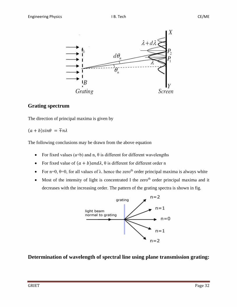
Grating spectrum
The direction of principal maxima is given by
(𝑎 + 𝑏)𝑠𝑖𝑛𝜃 = ∓𝑛𝜆
The following conclusions may be drawn from the above equation
• For fixed values (a+b) and n, θ is different for different wavelengths
• For fixed value of (𝑎 + 𝑏)𝑎𝑛𝑑𝜆, θ is different for different order n
• For n=0, θ=0, for all values of λ. hence the zeroth order principal maxima is always white
• Most of the intensity of light is concentrated I the zeroth order principal maxima and it
decreases with the increasing order. The pattern of the grating spectra is shown in fig.
Determination of wavelength of spectral line using plane transmission grating:

Engineering Physics I B. Tech CE/ME
GRIET Page 33
In the lab, the grating spectrum of a given source of light is obtained by using a spectrometer.
Initially all the adjustments of the spectrometer are made and it is adjusted for parallel rays by
Schuster’s method.
The slit is illuminated by monochromatic light (sodium lamp) and the position of telescope is
adjusted, such that the image of the slit is obtained at the position of the vertical cross wire in the
field of view of the telescope.
If the wavelength if the sodium light is to be determined, then the angles of diffraction – and –
corresponding to the first and second order principal maxima are determined.
OA, OB etc gives the direction of the telescope corresponding to the first and second order
images.
(𝑎 + 𝑏) sin 𝜃1 = 1𝜆. . (1)
(𝑎 + 𝑏) sin 𝜃2 = 2𝜆. . (2)
Then the value of λ is calculated from equation (1,2) and the mean value is taken.
(𝑎 + 𝑏) is the grating element and it is equal to the reciprocal of the number of lines per cm.
If the number of lines on the grating surface is 15,000 per inch, then
(𝑎 + 𝑏) =2.54
15000𝑐𝑚 ( 1 𝑖𝑛𝑐ℎ = 2.54 𝑐𝑚)

Engineering Physics I B. Tech CE/ME
GRIET Page 34
If the source of the light emits radiations of different wavelengths, then the beam gets
disappeared by the grating and in each order a spectrum of the constituent wavelengths is
observed.
Previous Questions:
2 Marks
1. Define Interference, what are the conditions to get the maximum and minimum intensity
of light.
2. What is principle of superposition of two waves
3. What is diffraction?
4. Explain the differences between Fresnel and Fraunhoffer diffraction?
5. Write the differences between interference and diffraction?
Essay Questions:
1. a) What are Newton’s rings? Describe and explain the formation of Newton’s rings in
reflected monochromatic light. Prove that in reflected light, (a) Diameters of the dark
rings are proportional to the square root of natural numbers, and (2) Diameters of the
bright rings are proportional to the square root of odd natural numbers.
2. Explain how wavelength of monochromatic light is determined by Newton’s rings
method.
3. Explain the colors when a thin film illuminated by white light is observed in reflected
light.
4. What is diffraction of light? Derive an expression for the intensity distribution due to
Fraunhoffer diffraction at a single slit and show that the intensity of the first subsidiary
maxima is about 4.5% of that of the principal maximum.
5. Discuss the Fraunhoffer diffraction due to N- slits and obtain the intensity distribution
and positions of maxima and minima and derive expression for resolving power of a
grating.

Engineering Physics I B. Tech CE/ME
GRIET Page 35
UNIT- II
LASERS & FIBER OPTICS
LASER: Light Amplification by Stimulated Emission of Radiation
Characteristics of Laser Beam: Some of the special characteristics which distinguish
lasers from ordinary light sources are
• High Directionality
• High Intensity
• Highly Monochromatic
• Highly Coherent
• High Directionality:
Laser emits radiation only in one direction. The directionality of laser beam is expressed in terms
of angle of divergence (ᶲ)
Divergence or Angular Spread is given by ∅ =𝑟2−𝑟1
𝑑2−𝑑1
Where d1, d2 are any two distances from the laser source emitted and
r1, r2 are the radii of beam spots at a distance d1 and d2 respectively as shown in above figure.
Laser light having less divergence, it means that laser light having more directionality.
• High Intensity: Generally, light from conventional source spread uniformly in all
directions. For example, take 100 watt bulb and look at a distance of 30 cm, the power
enter into the eye is less than thousand of a watt. This is due to uniform distribution of
light in all directions.
But in case of lasers, light is a narrow beam and its energy is concentrated within the small
region. The concentration of energy accounts for greater intensity of lasers.

Engineering Physics I B. Tech CE/ME
GRIET Page 36
• Highly Monochromatic: The light emitted by laser is highly monochromatic than
any of the other conventional monochromatic light. A comparison between normal light
and laser beam, ordinary sodium (Na) light emits radiation at wave length of 5893A0 with
the line width of 1A0. But He-Ne laser of wave length 6328A0 with a narrow width of
only 10-7 A0 i.e., Monochromacity of laser is 10 million times better than normal light.
The degree of Monochromacity of the light is estimated by line of width (spreading frequency of
line).
• Highly Coherent: If any wave appears as pure sine wave for longtime and infinite space,
then it is said to be perfectly coherent.
Practically, no wave is perfectly coherent including lasers. But compared to other light sources,
lasers have high degree of coherence because all the energy is concentrated within the small
region. There are two independent concepts of coherence.
i) Temporal coherence (criteria of time)
ii) Spatial coherence (criteria of space)
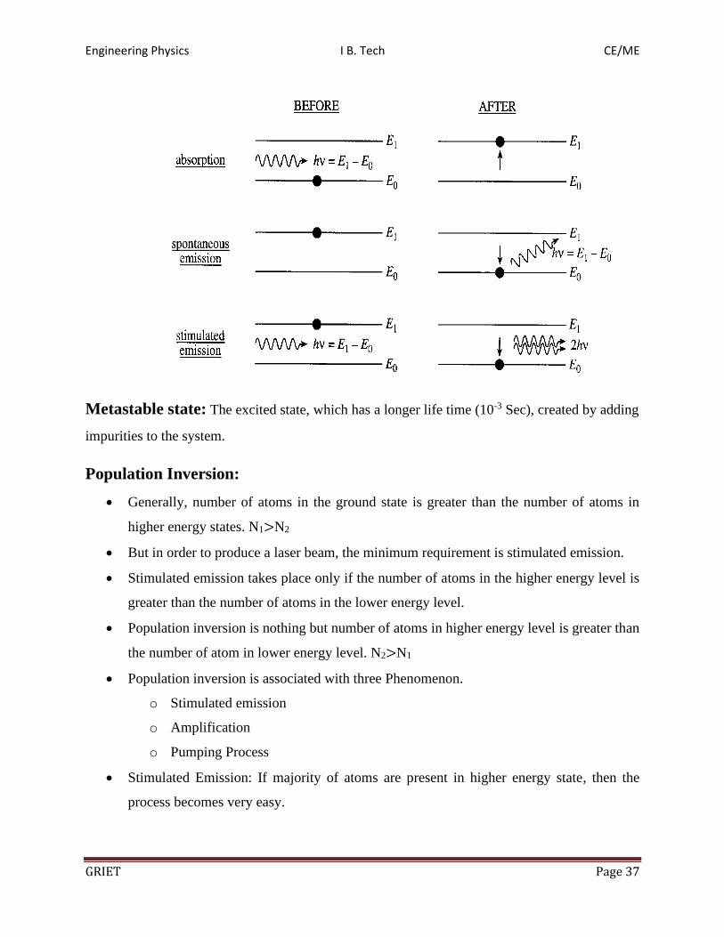
Absorption, Spontaneous emission, stimulated emission:
• Absorption: When at atom absorbs an amount of energy ‘hv’ in the form of photon from
the external agency and excited into the higher energy levels from ground state, then this
process is known as absorption. Atom + hv atom*
• Spontaneous Emission: When an atom in the excited state emits a photon of energy ‘hv’
coming down to ground state by itself without any external agency, such an emission is
called spontaneous emission. Atom* atom + hv
• Photons released in spontaneous emission are not coherent. Hence spontaneous emission
is not useful for producing lasers.
• Stimulated Emission: When an atom in the excited state, emits two photons of same
energy ‘hv’ while coming to down to ground state with the influence of an external
agency, such an emission is called stimulated emission. Atom* atom + 2hv
• In the two photons one photon induces the stimulated emission and the second one is
released by the transition of atom from higher energy level to lower energy level.
• Both the photons are strictly coherent. Hence stimulated emission is responsible for laser
production.
Engineering Physics I B. Tech CE/ME
GRIET Page 37
Metastable state: The excited state, which has a longer life time (10-3 Sec), created by adding
impurities to the system.
Population Inversion:
• Generally, number of atoms in the ground state is greater than the number of atoms in
higher energy states. N1>N2
• But in order to produce a laser beam, the minimum requirement is stimulated emission.
• Stimulated emission takes place only if the number of atoms in the higher energy level is
greater than the number of atoms in the lower energy level.
• Population inversion is nothing but number of atoms in higher energy level is greater than
the number of atom in lower energy level. N2>N1
• Population inversion is associated with three Phenomenon.
o Stimulated emission
o Amplification
o Pumping Process
• Stimulated Emission: If majority of atoms are present in higher energy state, then the
process becomes very easy.

Engineering Physics I B. Tech CE/ME
GRIET Page 38
• Amplification: If ‘N1’, represents number of atoms in the ground state and ‘N2’ represents
number of atoms in the excited state than the amplification of light takes place only when
N2> N1.
• If N2> N1, there will be a population inversion. So induced beam and induced emission
are in the same directions and strictly coherent, then the resultant laser is said to be
amplified.
• Boltzmann’s principle gives the information about the fraction of atom found on average
in any particulars energy state at equilibrium temperature as
• 𝑁1
𝑁2= exp (𝐸2-E1/KT) =exp (∆𝐸/KT)
𝑁1
𝑁2= exp (hv/KT)
Pumping
The process, which excites the atoms from ground state to excited state to achieve population
inversion.
Pumping can be done by number of ways
• Optical Pumping excitation by strong source of light (flashing of a
Camera, xenon flash lamp)
• Electrical Pumping excitation by electron impact
• Chemical Pumping excitation by chemical reactions
• Direct Conversion Electrical energy is directly converted into radiant Energy
in devices like LED’s, population Inversion is achieved in forward bias.
Principle of laser/lasing action
Laser Production Principle:
• Two coherent photons produced in the stimulated emission, interacts with other two
excited atoms, resulting in four coherent photons.
• Thus, coherent photons are multiplied in a lasing medium. The continuous successive
emission of photons results for the production of laser beam.

Engineering Physics I B. Tech CE/ME
GRIET Page 39
Einstein’s Theory of Radiation (Einstein’s Coefficients)
• In 1917, Einstein predicted the existence of two different kinds of processes by which an
atom emits radiation.
• Transition between the atomic energy states is statistical process. It is not possible to
predict which particular atom will make a transition from one state to another state at a
particular instant. For an assembly of very large number of atoms it is possible to
calculate the rate of transitions between two states.
• Einstein was the first to calculate the probability of such transition, assuming the atomic
system to be in equilibrium with electromagnetic radiation.
• If N1 is the number of atoms in E1 state, N2 is the number of atoms in E2 state. 𝑈(𝛾)is the
enrgy incident on the system, then
• The probability of transmission of atoms form E1 to E2 state (stimulated absorption) is
𝑃12∞ 𝑈(𝛾)
𝑃12 = 𝐵12 𝑈(𝛾)
𝑁1𝑃12 = 𝑁1𝐵12 𝑈(𝛾)….. (1)
𝐵12 = 𝑃𝑟𝑜𝑝𝑜𝑟𝑡𝑖𝑜𝑎𝑛𝑙 𝑐𝑜𝑛𝑠𝑡𝑎𝑛𝑡
• The probability of transmission of atoms form E2 to E1 state (spontaneous emission) is
𝑁2𝑃21 = 𝑁2𝐴21
The number of spontaneous transitions Nsp taking place in time‘t’ depends on only
number of atoms N2 lying in excited state.
• The probability of transmission of atoms form E2 to E1 state (spontaneous emission) is
𝑃21 ∞ 𝑈(𝛾)
𝑁2𝑃21 = 𝑁2𝐵21 𝑈(𝛾)

Engineering Physics I B. Tech CE/ME
GRIET Page 40
Therefore the numbers of downward transitions are
𝑁2𝑃21 = 𝑁2𝐴21 + 𝑁2𝐵21 𝑈(𝛾)… (2)
• Under the thermal equilibrium, number of upward transitions = number of downward
transitions per unit volume per second.
• 𝑁1𝑃12 = 𝑁2𝑃21
From (1) and (2)
𝑁1𝐵12 𝑈(𝛾) = 𝑁2𝐴21 + 𝑁2𝐵21 𝑈(𝛾)
𝑈(𝛾)[𝑁1𝐵12 − 𝑁2𝐵21] = 𝑁2𝐴21
𝑈(𝛾) =𝑁2𝐴21
[𝑁1𝐵12 − 𝑁2𝐵21]
𝑈(𝛾) =𝑁2𝐴21
𝑁2𝐵21[𝑁1𝐵12 − 1]
𝑈(𝛾) =
𝐴21𝐵21
[𝑁1𝑁2
𝐵12𝐵21
−1]….. (3)
According to Maxwell- Boltzmann statistics,
𝑁1
𝑁2= 𝑒𝑥𝑝
ℎ𝛾
𝐾𝐵𝑇 … . . (4) in (3)
𝑈(𝛾) =
𝐴21𝐵21
[𝑒𝑥𝑝
ℎ𝛾𝐾𝐵𝑇 𝐵12
𝐵21−1]
…(4)
On comparing eq (4) with Planck’s theory of black body radiation
𝑈(𝛾) =8𝜋𝛾2𝑑𝛾
𝑐3
1
𝑒𝑥𝑝
ℎ𝛾𝐾𝐵𝑇 −1
… (5)
𝑐𝑜𝑚𝑝𝑎𝑟𝑖𝑛𝑔 𝑒𝑞(4)𝑎𝑛𝑑 (5)
𝐴21
𝐵21=
8𝜋𝛾2𝑑𝛾
𝑐3
𝐴21
𝐵21∞ 𝛾2…. (6)
𝐵12
𝐵21= 1
𝐵12 = 𝐵21..(7)
𝐸𝑞𝑛 (6), (7)𝑎𝑟𝑒 𝑐𝑎𝑙𝑙𝑒𝑑 𝑎𝑠 𝐸𝑖𝑛𝑠𝑡𝑒𝑖𝑛′𝑠 𝑟𝑒𝑙𝑎𝑡𝑖𝑜𝑛𝑠
The coefficients A21, B12, B21 are known as Einstein coefficients.

Engineering Physics I B. Tech CE/ME
GRIET Page 41
Note: Since we are applying same amount of energy (Q) and observing in the same time
(t), number of atoms excited into higher energy levels (absorption) = number of atoms
that made transition into lower energy levels (stimulated emission)
B12 = B21i.e. Absorption = stimulated emission
Ruby Laser: It is a 3 level solid state laser, discovered by Dr.T.Maiman in 1960.
Principle:
• The chromium Ions raised to excited states by optical pumping using xenon flash lamp
• Then the atoms are accumulated at metastable state by non-radiative transition.
• Due to stimulated emission the transition of atoms take place from metastable state to
ground state, there by emitting laser beam.
Construction:
• Ruby is a crystal of aluminum oxide (Al2O3) in which some of the aluminum ions (Al3+)
is replaced by chromium ions (Cr3+). This is done by doping small amount (0.05%) of
chromium oxide (Cr2O3) in the melt of purified Al2O3.
• These chromium ions give the pink color to the crystal. Laser rods are prepared from a
single crystal of pink ruby. Al2O3 does not participate in the laser action. It only acts as
the host.

Engineering Physics I B. Tech CE/ME
GRIET Page 42
• The ruby crystal is in the form of cylinder. Length of ruby crystal is usually 2 cm to 30
cm and diameter 0.5 cm to 2 cm.
• The ends of ruby crystal are polished, grounded and made flat.
• The one of the ends is completely silvered while the other one is partially silvered to get
the efficient output. Thus the two polished ends act as optical resonator system.
• A helical flash lamp filled with xenon is used as a pumping source. The ruby crystal is
placed inside a xenon flash lamp. Thus, optical pumping is used to achieve population
inversion in ruby laser.
• As very high temperature is produced during the operation of the laser, the rod is
surrounded by liquid nitrogen to cool the apparatus.
Working with Energy Level Diagram (ELD):
Fig: Energy Level Diagram of Ruby Laser
• The flash lamp is switched on, a few thousand joules of energy is discharged in a few
milliseconds.
• A part of this energy excites the Cr3+ Ions to excited state from their ground state and the
rest heats up the apparatus can be cooled by the cooling arrangement by passing liquid
nitrogen.
• The chromium ions respond to this flash light having wavelength 5600 A0(Green),[4200
A0(Red)Also]
• When the Cr3+ Ions are excited to energy level E3 from E1 the population in E3 increases.

Engineering Physics I B. Tech CE/ME
GRIET Page 43
• Cr3+ Ions stay here(E3) for a very short time of the order of 10-8 sec, then they drop to the
level E2 which is Metastable state of lifetime 10-3 sec .Here the transitions from E3 to E2
is non radiative in nature.
• As the lifetime of the state E2 is much longer, the number of ions in this state goes on
increasing while in the ground state (E1) goes on decreasing. By this process population
inversion is achieved between E2& E1.
• When an excited ion passes spontaneously from the Metastable state E2 to the ground
state E1 it emits a photon of wavelength 6943A0.
• This photon travels through the ruby rod and if it is moving parallel to the axis of the
crystal, is reflected back & forth by silvered ends until it stimulates an excited ion in E2
and causes it to emit fresh photon in phase with the earlier photon. This stimulated
transition triggers the laser Transition.
• The process is repeated again and again, because the photons repeatedly move along the
crystal being reflected from ends. The photons thus get multiplied.
• When the photon beam becomes sufficiently intense, such that a part of it emerges
through the partially silvered end of the crystal.
Helium –Neon (He-Ne) Laser:
Principle: This laser is based on the principle of stimulated emission, produced in the active
medium of gas. Here, the population inversion achieved due to the interaction between the two
gases which have closed higher energy levels.
Construction:
▪ Fig: He-Ne laser

Engineering Physics I B. Tech CE/ME
GRIET Page 44
• The first gas laser to be operated successfully was the He-Ne laser in 1961 by the
scientist A. Jawan.
• In this method, two gases helium & Neon were mixed in the ratio 10:1 in a discharge tube
made of quartz crystal.
• The dimensions of the discharge tube are nearly 80 cm length and 1.5 cm diameter, with
its windows slanted at Brewster’s angle i.e., = Tan-1(n) ,Where n = refractive index of
the window substance.
• The purpose of placing Brewster windows on either side of the discharge tube is to get
plane polarized laser output.
• Two concave mirrors M1& M2 are made of dielectric material arranged on both sides of
the discharge tube so that their foci lines within the interior of discharge tube.
• One of the two concave mirrors M1 is thick so that all the incident photons are reflected
back into lasing medium.
• The thin mirror M2 allows part of the incident radiation to be transmitted to get laser
output.
Working:
Fig:(E.L.D) Energy Level Diagram corresponding to He-Ne laser

Engineering Physics I B. Tech CE/ME
GRIET Page 45
• The discharge tube is filled with Helium at a pressure of 1 mm of Hg & Neon at 0.1mm
of Hg.
• When electric discharge is set-up in the tube, the electrons present in the electric field
make collisions with the ground state He atoms.
• Hence ground state He atoms get excited to the higher energy levels F1 (2S1), F2 (2S3).
• Here Ne atoms are active centers.
• The excited He atoms make collision with the ground state Ne atoms and bring the Ne
atoms into the excited states E4& E6.
• The energy levels E4& E6 of Ne are the metastable states and the Ne atoms are directly
pumped into these energy levels.
• Since the Ne atoms are excited directly into the levels E4& E6, these energy levels are
more populated than the lower energy levels E3&E5.
• Therefore, the population inversion is achieved between E6&E5,E6&E3,E4&E3
• The transition between these levels produces wavelengths of 3390 A0,6328 A0,1150 A0
respectively.
• Now The Ne atoms undergo transition from E3 to E2 and E5 to E2 in the form of fast
decay giving photons by spontaneous emission. These photons are absorbed by optical
elements placed inside the laser system.
• The Ne atoms are returned to the ground state (E1) from E2 by non radiative diffusion and
collision process, therefore there is no emission of radiation.
• Some optical elements placed inside the laser system are used to absorb the IR laser
wavelengths 3390 A0, 1150 A0.
• Hence the output of He-Ne laser contains only a single wavelength of 6328A0.
• The released photons are transmitted through the concave mirror M2 there by producing
laser.
• A continuous laser beam of red color at a wavelength of 6328A0.
• By the application of large potential difference, Ne atoms are pumped into higher energy
levels continuously.
• A Laser beam of power 0.5 to 50 MW comes out from He-Ne laser.

Engineering Physics I B. Tech CE/ME
GRIET Page 46
Important applications of Lasers in various fields
Applications of Lasers: Lasers have wide applications in different branches of science and
engineering because of the following.
• Very narrow band width
• High directionality
• Extreme brightness
Communication:
• Lasers are used in optical communications, due to narrow band width.
• The laser beam can be used for the communication b/w earth & moon (or) other satellites
due to the narrow angular speed.
• Used to establish communication between submarines i.e; under water communication.
Medical:
• Identification &curing of tumors.
• Used to detect and remove stones in kidneys.
• Used to detect tumors in brain.
Industry:
• Used to make holes in diamond and hard steel.
• Used to detect flaws on the surface of aero planes and submarines.
Chemical &Biological:
• Lasers have wide chemical applications. They can initiate or fasten chemical reactions.
• Used in the separation of isotopes.
• Lasers can be used to find the size & shape biological cells such as erythrocytes.

Engineering Physics I B. Tech CE/ME
GRIET Page 47
Optical Fibers
Optical fibers are the waveguides through which electromagnetic waves of optical frequency
range can be guided through them to travel long distances. An optical fiber works on the
principle of total internal reflection (TIR).
Advantages of optical fibers over coaxial metallic cables
• Optical fibers allow light signals of frequencies over a wide range and hence greater
volume of information can be transmitted either in digital form or in analog form within a
short time.
• In metallic cables only 48 conversations can be made at once without cross talks where as
in optical fibers more than 15000 conversations can be made at once without cross talks.
• Light cannot enter through the surface of the optical fiber except at the entry interface
i.e., interference b/w different communication channels is absent. Hence purity of light
signal is protected.
• Optical signal do not produce sparks like electrical signals and hence it is safe to use
optical fibers.
• External disturbances from TV or Radio Stations power electronic systems and lightening
cannot damage the signals as in case of metallic cables.
• Materials used in the manufacture of optical fibers are SiO2, plastic, glasses which are
cheaper & available in plenty.
Total Internal Reflection: when a light ray travels from a denser medium into a rarer
medium and if the angle of incidence is greater than the critical angle, then the light gets totally
reflected into the denser medium.

Engineering Physics I B. Tech CE/ME
GRIET Page 48
Structure of an optical fiber:
An optical fiber consists of three (3) co-axial regions.
• The inner most region is the light-guiding region known as “Core”. It is surrounded by a
middle co-axial regional known as “cladding”. The outer most regions which completely
covers the core & cladding regions is called “sheath or buffer jacket”.
• Sheath protects the core & cladding regions from external contaminations, in addition to
providing mechanical strength to the fiber.
• The refractive index of core (n1) is always greater than the refractive index of cladding
(n2) i.e., n1> n2 to observe the light propagation through structure of optical fiber.
• When light enters through one end of optical fiber it undergoes successive total internal
reflections and travel along the fiber in a “zig-zag” path.
Numerical Aperture:
Light gathering capacity of an optical fiber. It depends on two factors
• Core diameter
• NA
NA is defined as sin of the acceptance angle
NA = Sinθ0 = √n12 − n2
2
The efficiency of optical fiber is expressed in terms of NA; it is called as figure of merit of
optical fiber.
Engineering Physics I B. Tech CE/ME
GRIET Page 49
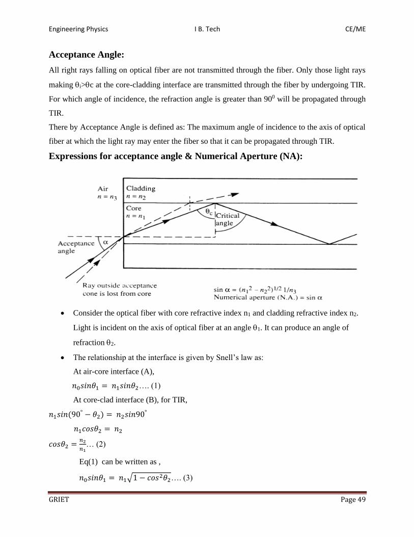
Acceptance Angle:
All right rays falling on optical fiber are not transmitted through the fiber. Only those light rays
making i>c at the core-cladding interface are transmitted through the fiber by undergoing TIR.
For which angle of incidence, the refraction angle is greater than 900 will be propagated through
TIR.
There by Acceptance Angle is defined as: The maximum angle of incidence to the axis of optical
fiber at which the light ray may enter the fiber so that it can be propagated through TIR.
Expressions for acceptance angle & Numerical Aperture (NA):
• Consider the optical fiber with core refractive index n1 and cladding refractive index n2.
Light is incident on the axis of optical fiber at an angle 1. It can produce an angle of
refraction 2.
• The relationship at the interface is given by Snell’s law as:
At air-core interface (A),
𝑛0𝑠𝑖𝑛𝜃1 = 𝑛1𝑠𝑖𝑛𝜃2…. (1)
At core-clad interface (B), for TIR,
𝑛1𝑠𝑖𝑛(90° − 𝜃2) = 𝑛2𝑠𝑖𝑛90°
𝑛1𝑐𝑜𝑠𝜃2 = 𝑛2
𝑐𝑜𝑠𝜃2 =𝑛2
𝑛1… (2)
Eq(1) can be written as ,
𝑛0𝑠𝑖𝑛𝜃1 = 𝑛1√1 − 𝑐𝑜𝑠2𝜃2…. (3)

Engineering Physics I B. Tech CE/ME
GRIET Page 50
Substituting (2) in (3),
𝑛0𝑠𝑖𝑛𝜃1 = 𝑛1√1 −𝑛2
2
𝑛12
𝑛0𝑠𝑖𝑛𝜃1 = √𝑛12 − 𝑛2
2
For air n0=1, 𝑠𝑖𝑛𝜃1 = √𝑛12 − 𝑛2
2
𝜃1 = 𝜃𝐴 = sin−1 √𝑛12 − 𝑛2
2
Here A is called Acceptance angle. This gives max value of external incident angle for
which light will propagate in the fiber.
Numerical Aperture (NA):
Numerical aperture is defined as light gathering capacity of an optical fiber which depends on
two factors i.e Core diameter & NA.The efficiency of optical fiber is expressed in terms of NA,
so it is called as figure of merit of optical fiber.
NA is defined as sine of the acceptance angle i.e.,
𝑁𝐴 = sin 𝜃𝐴
𝑁𝐴 = √𝑛12 − 𝑛2
2
𝑁𝐴 = √𝑛12 − 𝑛2
2 = √(𝑛1 − 𝑛2)(𝑛1 + 𝑛2)…(1)
Fractional index change
∆=𝑛1 − 𝑛2
𝑛1
∆ 𝑛1 = 𝑛1 − 𝑛2..(2) in (1)
Engineering Physics I B. Tech CE/ME
GRIET Page 51
𝑁𝐴 = √∆ 𝑛1(𝑛1 + 𝑛2)
Let 𝑛1 = 𝑛2, 𝑡ℎ𝑒𝑛 𝑛1 + 𝑛2 = 2𝑛1
Then 𝑁𝐴 = √∆ 𝑛1 − 2𝑛1 = 𝑛1√2∆
Classification of Optical Fibers:
Optical fibers are classified into 3 major categories based on
1) Material
2) Number of modes and
3) Refractive Index Profile
• Based on the materials in which the fibers arc made it is classified into two types as
follows
Glass fibers: If the fibers are made up of mixture of metal oxides and silica glasses then they are
called as glass fibers.
Plastic fibers: If the fibers are made up of plastics and they are called plastic optical fibers.
• Based on variation in the core refractive index (n1), optical fibers are divided into two
types
1. Step index fiber
2. Graded index fiber
• Based on mode of propagation, fibers are further classified in to
1. Single mode propagation (Step index fibers have both single & multimode propagations)
2. Multi mode propagation (Graded index fibers have multimode propagation only)
• All together in total three (3) types of fibers
1. Single mode step index fiber
2. Multi mode step index fiber
3. Multi mode graded index fiber
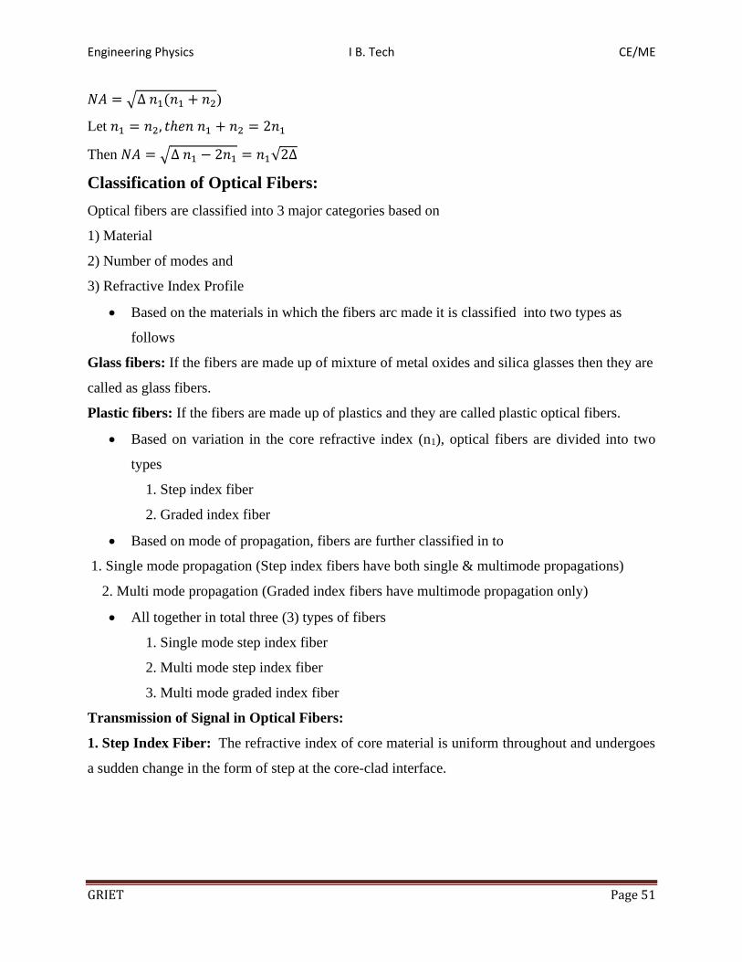
Transmission of Signal in Optical Fibers:
1. Step Index Fiber: The refractive index of core material is uniform throughout and undergoes
a sudden change in the form of step at the core-clad interface.

Engineering Physics I B. Tech CE/ME
GRIET Page 52
Fig: Refractive index profile & propagation in single mode, step index& graded index
fibers
a) Single Mode Step Index Fiber:
• The variation of the refractive index of a step index fiber as a function of distance can be
mathematically represented as longitudinal cross section.
Note: Mode of propagation: It is defined as the number of paths available for the light ray to
transfer through the optical fiber.
Structure:
i) Core Diameter: 8 to 12 m, usually 8.5m
ii) Cladding Diameter: Around 125m
iii) Sheath Diameter: 250 to 1000 m
iv) NA: 0.08 to 0.15 usually 0.10
Performance Characteristics:
i) Band Width: Greater than 500 MHZ Km.
ii) Attenuation: 2 to 5 dB / Km.
iii) Applications: These fibers are ideally suited for high band width applications using single
mode injection coherent (LASER) sources.
b) Multi Mode Step Index Fibers:
• These fibers have reasonably large core diameters and large NA to facilitate efficient
transmission to incoherent or coherent light sources.

Engineering Physics I B. Tech CE/ME
GRIET Page 53
• These fibers allow finite number of modes.
• Normalized frequency (NF) is the cut off frequency, below which a particular mode
cannot exist. This is related to NA, Radius of the core, and wave length of light as
NF =2 𝜋/λ a (NA), Where a = radius of core
Structure:
i) Core Diameter: 50 to 200 m
ii) Cladding Diameter: 125 to 400 m
iii) Sheath Diameter: 250 to 1000 m
iv) NA: 0.16 to 0.5
Performance Characteristics:
i) Band Width: 6 to 50 MHZ Km.
ii) Attenuation: 2.6 to 50 db/km.
iii) Applications: These fibers are ideally suited for limited band width and relatively low cost
applications.
c) Multi Mode Graded Index Fibers:
• In case of graded index fibers, the refractive index of core is made to vary as a function
of radial distance from the centre of the optical fiber.
• Refractive index increases from one end of core diameter to center and attains maximum
value at the centre. Again refractive index decreases as moving away from center to
towards the other end of the core diameter.
• The refractive index variation is represented as n(r) = n1(1-2Δ)1/2 = n2
Here Δ = fractional change in refractive index = n1-n2/n1
• The number of modes is given by the expression N = 4.9[d(NA)/ λ]2
Where d = core diameter, λ = wavelength of radiation
Structure:
i) Core Diameter: 30 to 100 m
ii) Cladding Diameter: 105 to 150 m
iii) Sheath Diameter: 250 to 1000 m
iv) NA: 0.2 to 0.3

Engineering Physics I B. Tech CE/ME
GRIET Page 54
Performance Characteristics:
i) Band Width: 300 MHZ Km to 3 GHZ Km.
ii) Attenuation: 2 to 10 dB/km.
iii) Applications: These are ideally suited for medium to high band width applications using
incoherent and coherent multimode sources.
Distinguish Step index & Graded index fibers And Single mode & Multi mode
fibers?
Step Index Graded Index
1. RI of core is uniform throughout except
at one stage.
2. Single & multimode propagations exist.
3. Used for short distance applications.
4. Attenuation losses are of the order 100
dB/km.
5. Mer4dinol rays propagation takes place.
6. Easy to manufacture.
1. Refractive index varies gradually with
radial distance.
2. It is a multi mode fiber.
3. Used for long distance applications.
4. 4. Attenuation losses are of the order 10
dB/km.
5. Skew rays propagation takes place.
6. Difficult to manufacture.
Single Mode Multi Mode
1. Core diameter is small.
2. Signal entry is difficult.
3. Exists in step index fiber.
4. Light must be coherent.
1. Core diameter is large.
2. Signal entry is easy.
3. Exists in both step & graded index
fibers.
4. Light source may be coherent or
incoherent source.

Engineering Physics I B. Tech CE/ME
GRIET Page 55
Optical fiber communication link with help of block diagram
Optical Fiber Communication Link:
Fig:Block Diagram of Optical fiber communication link
Optical fiber is an ideal communication medium by systems that require high data capacity, fast
operation and to travel long distances with a minimum number of repeaters.
Encoder: It is an electronic system that converts the analog information signals, such as voice of
telephone user, in to binary data. The binary data consists of series of electrical pulses.
Transmitter: Transmitter consists of a driver which is a powerful amplifier along with light
source. The o/p of amplifier feeds to light source, which converts electrical pulses in to light
pulses.
Source to Fiber Connector: It is a special connector that sends the light from sources to fiber.
The connector acts as temporary joint b/w the fiber and light source, misalignment of this joint,
leads to loss of signal.,
Fiber to Detector Connector: It is also temporary joint, which collects the source from fiber.
Receiver: Receiver consists of a detector followed by amplifier. This combination converts light
pulses in to electrical pulses.
Engineering Physics I B. Tech CE/ME
GRIET Page 56
Decoder: Electrical pulses containing information are fed to the electronic circuit called decoder.
Decoder converts binary data of electrical pulses in to analog information signals.
Attenuation in optical fibers
Usually, the power of light at the output end of optical fiber is less than the power launched at
the input end, then the signal is said to be attenuated.
Attenuation: It is the ratio of input optical power (Pi) in to the fiber to the power of light coming
out at the output end (Po).
Attenuation coefficient is given as, α = 10/L log10 Pi / Po db/km.
Attenuation is mainly due to
1. Absorption.
2. Scattering.
3. Bending.
1. Absorption Losses:
In glass fibers, three different absorptions take place.
Ultra violet absorption: Absorption of UV radiation around 0.14µm results in the ionization of
valence electrons.
Infrared absorption: Absorption of IR photons by atoms within the glass molecules causes
heating. This produces absorption peak at 8µm, also minor peaks at 3.2, 3.8 and 4.4µm.
Ion resonance/OH- absorption: The OH- ions of water, trapped during manufacturing causes
absorption at 0.95, 1.25 and 1.39µm.
2. Scattering Losses:
The molten glass, when it is converted in to thin fiber under proper tension creates sub
microscopic variations in the density of glass leads to losses.
The dopents added to the glass to vary the refractive index also leads to the inhomogenities in the
fiber. As a result losses occur.
Scattering losses are inversely proportional to fourth power of λ.(λ4)
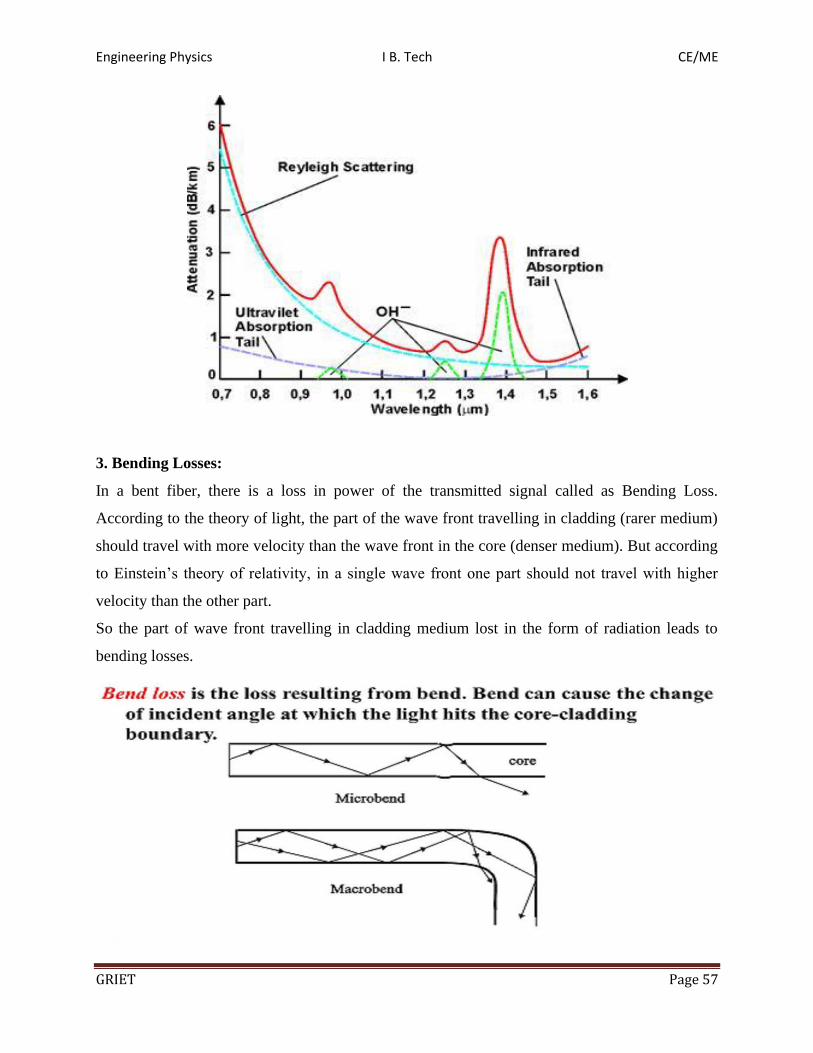
Engineering Physics I B. Tech CE/ME
GRIET Page 57
3. Bending Losses:
In a bent fiber, there is a loss in power of the transmitted signal called as Bending Loss.
According to the theory of light, the part of the wave front travelling in cladding (rarer medium)
should travel with more velocity than the wave front in the core (denser medium). But according
to Einstein’s theory of relativity, in a single wave front one part should not travel with higher
velocity than the other part.
So the part of wave front travelling in cladding medium lost in the form of radiation leads to
bending losses.

Engineering Physics I B. Tech CE/ME
GRIET Page 58
Applications of Optical fibers:
• As fibers are very flexible, they are used in flexible digital cameras.
• Fibers are used in mechanical imaging i.e. for inspection of mechanical welds in pipes
and engines of rockets, space shuttles, airplanes.
• They are used in medical imaging such as endoscopes and laparoscopes.
• Fibers can be used under sea communication.
• Fibers are used in military applications such as aircrafts, ships, tanks etc.
• Nuclear testing applications use optical fiber phase sensors and transducers
• Fibers are used in public utility organizations like railways, TV transmission etc.
• Fibers are used in LAN systems of offices, industrial plants and colleges etc.
• They are used in telecommunications such as voice telephones.
Previous Questions
2 Marks Questions:
1) Discuss properties/Characteristics of Laser Beam[ June15,Jan 14]
2) Explain the following 1) Metastable state 2) Population Inversion[June 15]
3) What is population inversion and optical pumping in a laser?[June 15,June 15 supply]
4) Define Acceptance angle and Numerical Aperture of optical fiber [ Jan 14]
5) Write down advantages of fiber optics in communication systems [June 15]
Essay Questions:
1) Derive the relation between Einstein’s Coefficients [June 15, June 13]/how population
Inversion is achieved? Derive the relation between the probabilities of spontaneous emission
& stimulated emission in terms of Einstein’s coefficients.[Jan 14,July 12,feb 12]
2) Describe principle, working and construction of ruby laser [June15,July 12]
3) Illustrate on the construction and working principle of a He-Ne laser giving its energy
Level diagram [June 15, June 13, Feb 12, Feb 13, June 15]

Engineering Physics I B. Tech CE/ME
GRIET Page 59
4) Describe the construction and working of semiconductor diode laser with relevant energy
Level Diagram [Dec 15, Jan 14]
5) Write down any four applications of lasers [June 15]
6) Write an essay on the basic principle, construction, working of an optical fiber and
Advantages of Optical fiber [Feb 13,Jan 14]
7) Derive an expression for Acceptance angle and Numerical Aperture of an Optical Fiber
[June 13, Feb 12, Feb 13]
8) Explain the following i) single mode optical fiber ii) multi mode optical fiber iii) step
Index optical Fiber IV) graded index optical fiber [June 15]/ Discuss the refractive index of
Graded index and step index fibers [June 13, June 15]
9) Explain the Principle of optical fiber communication and write a note on attenuation
[June 15]
10) What is attenuation and explain different losses in optical fibers?[Jan 14,Dec 15,July 12]
11) Explain optical fiber communication link with block diagram [June 15, Dec 15, Feb 13]
12) An optical fiber has a core material of refractive index 1.55 and cladding material of
Refractive index 1.50. The light is launched from air. Calculate its numerical aperture
[Ans: 0.391][Feb 13]
UNIT –III
INTRODUCTION TO SOLIDS
Energy levels – Fermi Dirac Distribution:
According to the Quantum theory quantization leads to discrete energy levels. The electrons are
distributed among these energy levels according to Pauli’s exclusions principle i.e., it allows a
maximum number of two electrons with spins in opposite directions in any energy level. The pair
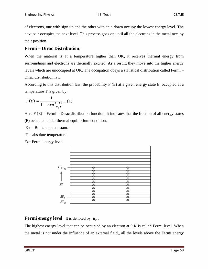
Engineering Physics I B. Tech CE/ME
GRIET Page 60
of electrons, one with sign up and the other with spin down occupy the lowest energy level. The
next pair occupies the next level. This process goes on until all the electrons in the metal occupy
their position.
Fermi – Dirac Distribution:
When the material is at a temperature higher than OK, it receives thermal energy from
surroundings and electrons are thermally excited. As a result, they move into the higher energy
levels which are unoccupied at OK. The occupation obeys a statistical distribution called Fermi –
Dirac distribution law.
According to this distribution law, the probability F (E) at a given energy state E, occupied at a
temperature T is given by
𝐹(𝐸) =1
1 + 𝑒𝑥𝑝𝐸−𝐸𝐹
𝐾𝐵𝑇
… (1)
Here F (E) = Fermi – Dirac distribution function. It indicates that the fraction of all energy states
(E) occupied under thermal equilibrium condition.
KB = Boltzmann constant.
T = absolute temperature
EF= Fermi energy level
Fermi energy level: It is denoted by 𝐸𝐹 .
The highest energy level that can be occupied by an electron at 0 K is called Fermi level. When
the metal is not under the influence of an external field,, all the levels above the Fermi energy

Engineering Physics I B. Tech CE/ME
GRIET Page 61
level are empty and those lying below are completely filled. Therefore Fermi level separates
filled and unfilled energy levels at 0K.
Each energy level can provide only two electrons: one for spin up and the other for spin down.
Therefore only two electrons can be filled in a given energy state and Pauli’s exclusion principle
is satisfied.
At T=0 K, if there are ‘N’ number of electrons (N being even), then we have 𝑁
2 number of filled
energy levels and other high energy levels will be completely empty.
Thus 𝑁
2th level is the highest filled energy level called as Fermi Energy Level (EF)
Importance:
Fermi energy level is maximum energy level up to which the electrons can be filled at 0K.
It acts as a reference level which separates the vacant and filled states at 0K.
It gives information about the filled electron states and empty states.
When the temperature is increased, few electrons gain the thermal energy and goes to higher
energy levels.
Effect of temperature on Fermi Function:
At 0K:-
From eqn (1), at Ok, the electrons can be filled only up to a maximum energy level called Fermi
energy level (EF0), above (EF0), all the energy level will be empty. It can be proved from the
following equations.
When 𝑬 < 𝑬𝑭: 𝐹(𝐸) = 1
1+𝑒−∞ =1
1= 1
100% chance for electrons to be filled below Fermi energy level.
When 𝑬 > 𝑬𝑭:𝐹(𝐸) = 1
1+𝑒∞ =1
∞= 0
0% chance for the electron to be filled above Fermi energy level.
When 𝑬 = 𝑬𝑭: 𝐹(𝐸) = 1
1+1=
1
2= 0.5
50% chance for an electron to be filled and not to be filled within the Fermi energy level
When temperature is raised slowly from absolute zero, F(E) smoothly decreases to zero.The
dotted lines show the change in energy of electrons at room temperature.

Engineering Physics I B. Tech CE/ME
GRIET Page 62
Electrons in a periodic potential –Bloch Theorem:
Inside a real crystal, there is a periodic arrangement of +vely charged ions through which the
electron moves as shown in fig (a). As an electron moves through +ve ion sites, it experiences
varying potential. The potential of the electron at the +ve ions site is zero and is maximum in
between two +veions sites.
So along any line passing through the centers of ions, the potential variation must be as in fig (b,
c)
Bloch’s theorem:
Schrodinger time independent equation is necessary to study the motion of an electron in a
periodic potential and to calculate its energy states.

Engineering Physics I B. Tech CE/ME
GRIET Page 63
𝑑2ψ
𝑑𝑥2+
8𝜋2𝑚(𝐸 − 𝑉)
ℎ2ψ = 0 … (1)
Now the potential V(x) has the periodicity of lattice by
𝑉(𝑥) = 𝑉(𝑥 + 𝑎). . (2)
a= periodicity of the lattice
According to Bloch, the solution of eqn (1) can be
ψ(x) = uk(x)eikx … (3)
eikx is a plane wave with periodicity
uk(x) = uk(x + a) … . (4)
‘k’ represents the state of motion of an electron having a momentum p =kh
2π and de-Broglie
wavelength λ =2π
k
Eqn (3) can be written as
ψ(x + a) = uk(x + a)eik(x+a)
From (4)
ψ(x + a) = uk(x)eik(x+a)
ψ(x + a) = uk(x)eik(x)eik(a)
From (3)
ψ(x + a) = ψ(x)eik(a) … . (5)
This is called Bloch condition
Similarly complex conjugate is
ψ∗(𝑥 + 𝑎) = ψ∗(𝑥)e−ik(a) … (6)
ψ(𝑥 + 𝑎)ψ∗(𝑥 + 𝑎) = ψ(x)ψ
∗(𝑥)
i.e the electron is not localized to any particular atom and probability of finding the electron is
same throughout the crystal.
KRONIG- PENNY MODEL:-
To overcome the complication in solving the Schrodinger wave equation for a nonlinear periodic
function of an electron in a metal given by Bloch, Kronig-penny introduced a simple model for
the shape of potential variation. The potential inside the crystal is approximated to the shape of
rectangular steps.
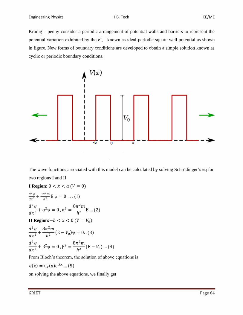
Engineering Physics I B. Tech CE/ME
GRIET Page 64
Kronig – penny consider a periodic arrangement of potential walls and barriers to represent the
potential variation exhibited by the eˉ, known as ideal-periodic square well potential as shown
in figure. New forms of boundary conditions are developed to obtain a simple solution known as
cyclic or periodic boundary conditions.
The wave functions associated with this model can be calculated by solving Schrödinger’s eq for
two regions I and II
I Region: 0 < 𝑥 < 𝑎 (𝑉 = 0)
𝑑2ψ
𝑑𝑥2 +8𝜋2𝑚
ℎ2 E ψ = 0 … (1)
𝑑2ψ
𝑑𝑥2+ α2ψ = 0 , α2 =
8𝜋2𝑚
ℎ2E … (2)
II Region:−𝑏 < 𝑥 < 0 (𝑉 = 𝑉0)
𝑑2ψ
𝑑𝑥2+
8𝜋2𝑚
ℎ2(E − 𝑉0)ψ = 0. . (3)
𝑑2ψ
𝑑𝑥2+ β2ψ = 0 , β2 =
8𝜋2𝑚
ℎ2(E − 𝑉0) … (4)
From Bloch’s theorem, the solution of above equations is
ψ(x) = uk(x)eikx … (5)
on solving the above equations, we finally get

Engineering Physics I B. Tech CE/ME
GRIET Page 65
𝛽2 − 𝛼2
2𝛼𝛽𝛽𝑏 sin 𝛼 𝑎 + cos 𝛼𝑎 = cos 𝑘𝑎 … (6)
𝛽2 − 𝛼2 = 8𝜋2𝑚
ℎ2(E − 𝑉0) −
8𝜋2𝑚
ℎ2E (from 2,4)
8𝜋2𝑚𝑉0
2𝛼𝛽ℎ2 𝛽𝑏 sin 𝛼 𝑎 + cos 𝛼𝑎 = cos 𝑘𝑎 … (7) M/D with a
4𝜋2𝑚𝑉0
ℎ2
𝑎𝑏 sin 𝛼 𝑎
𝛼𝑎+ cos 𝛼𝑎 = cos 𝑘𝑎 … (7)
𝑃 sin 𝛼 𝑎
𝛼𝑎+ cos 𝛼𝑎 = cos 𝑘𝑎 … (8)
P =4𝜋2𝑚𝑉0
ℎ2 𝑎𝑏 … (9)
𝑉0𝑎𝑏 = 𝑏𝑎𝑟𝑟𝑖𝑒𝑟 𝑠𝑡𝑟𝑒𝑛𝑔ℎ𝑡 𝑎𝑛𝑑 ′𝑝′𝑖𝑠 𝑐𝑎𝑙𝑙𝑒𝑑 𝑠𝑐𝑎𝑡𝑡𝑒𝑟𝑖𝑛𝑔 𝑝𝑜𝑤𝑒𝑟 𝑜𝑓 𝑝𝑜𝑡𝑒𝑛𝑡𝑖𝑎𝑙 𝑏𝑎𝑟𝑟𝑖𝑒𝑟
A graph is drawn for different 𝛼 values and at 𝑝 =3𝜋
2, it looks like below graph
Conclusion from Kronig –Penny Model:
• The allowed ranges of 𝛼𝑎 which permit a wave mechanical solution to exist are shown by
the shaded portions. Thus the motion of electrons in periodic lattices is characterized by
the bands of allowed energy separated by forbidden region.
• As the value of 𝛼𝑎 increases, the width of allowed energy bands also increases and the
width of the forbidden bands decreases.
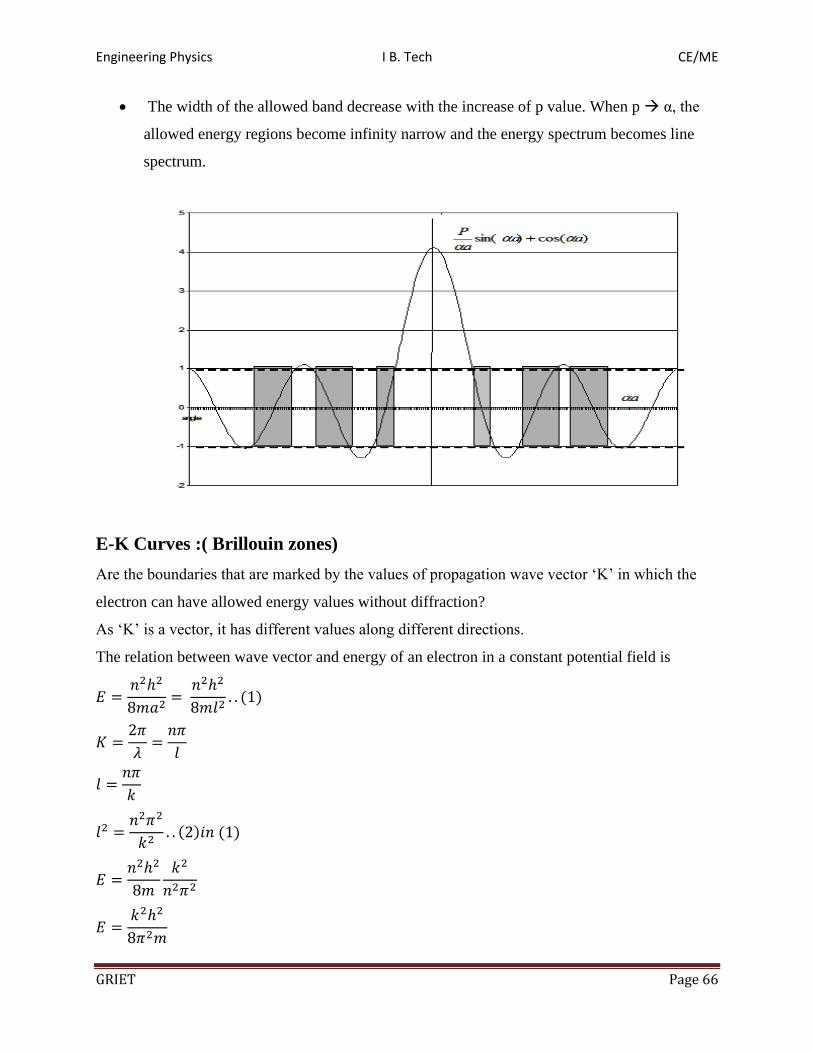
Engineering Physics I B. Tech CE/ME
GRIET Page 66
• The width of the allowed band decrease with the increase of p value. When p → α, the
allowed energy regions become infinity narrow and the energy spectrum becomes line
spectrum.
E-K Curves :( Brillouin zones)
Are the boundaries that are marked by the values of propagation wave vector ‘K’ in which the
electron can have allowed energy values without diffraction?
As ‘K’ is a vector, it has different values along different directions.
The relation between wave vector and energy of an electron in a constant potential field is
𝐸 =𝑛2ℎ2
8𝑚𝑎2=
𝑛2ℎ2
8𝑚𝑙2. . (1)
𝐾 =2𝜋
𝜆=
𝑛𝜋
𝑙
𝑙 =𝑛𝜋
𝑘
𝑙2 =𝑛2𝜋2
𝑘2. . (2)𝑖𝑛 (1)
𝐸 =𝑛2ℎ2
8𝑚
𝑘2
𝑛2𝜋2
𝐸 =𝑘2ℎ2
8𝜋2𝑚

Engineering Physics I B. Tech CE/ME
GRIET Page 67
A plot is drawn between E and K for different values of ‘n’ and the curves are shown below.
Electron can go from one Brillouin zone to another zone if it is supplied with energy equal to
forbidden zone or energy gap.
n = 1 = first Brillouin Zone (−𝜋
𝑎 𝑡𝑜
𝜋
𝑎)
n =2 = second Brillouin Zone (−2𝜋
𝑎 𝑡𝑜
2𝜋
𝑎)
Effective mass of the electron moving in a crystal lattice:

Engineering Physics I B. Tech CE/ME
GRIET Page 68
It has been known for a very long time that an electron has a well-defined mass, and when
accelerated by an electric field, it obeys Newtonian mechanics.
What happen when electron is to be accelerates inside a crystal/how will it react to an electric
field?
The mass of an electron in crystal appears, in general different from the free electron mass and is
called effective mass
When an electron in a periodic potential of lattice is accelerated by an electric field or magnetic
field, then the mass of an electron is called Effective mass (m*)
Let us consider an electron of charge ‘e’ and mass ‘m’ moving inside a crystal lattice when
subjected to an electric field ‘E’. The electrical force on an electron is 𝐹 = 𝑚𝑎∗
The acceleration 𝑎 =𝑒𝐸
𝑚 is not a constant in the periodic lattice of the crystal. It can be
considered by the variation of electron mass when it moves in the crystal lattice.
𝑎 =𝑒𝐸
𝑚∗… (1)
The velocity of an electron in a one-dimensional lattice is described by its group velocity given
by
𝑣𝑔 =𝑑𝑤
𝑑𝑘= 2𝜋
𝑑𝛾
𝑑𝑘=
2𝜋
ℎ
𝑑𝐸
𝑑𝑘. . (2)
Acceleration is 𝑎 =2𝜋
ℎ
𝑑
𝑑𝑡(
𝑑𝐸
𝑑𝑘)
𝑎 =2𝜋
ℎ
𝑑2𝐸
𝑑𝑘2
𝑑𝑘
𝑑𝑡… (3)
In (3), the quantity 𝑑2𝐸
𝑑𝑘2 is known form E and K relation. And we have to know the value of 𝑑𝑘
𝑑𝑡
under the influence of an applied field ‘E’.
Le an electron be subjected to the influence of an external filed of strength ‘E’ for a time ‘dt’. If
the velocity of electron is ‘v’, the distance travelled in a time 𝑑𝑡 𝑖𝑠 𝑣𝑑𝑡
So that 𝑑𝐸 = 𝑒𝐸𝑣𝑑𝑡 … (4)
Substitute (2) in (4)
𝑑𝐸 = 𝑒𝐸2𝜋
ℎ
𝑑𝑘
𝑑𝑡 𝑑𝑡
𝑑𝑘
𝑑𝑡= 𝑒𝐸
2𝜋
ℎ… (5)𝑖𝑛 (3)

Engineering Physics I B. Tech CE/ME
GRIET Page 69
𝑎 =2𝜋
ℎ
𝑑2𝐸
𝑑𝑘2
2𝜋
ℎ𝑒𝐸
𝑎 =4𝜋2
ℎ2𝑒𝐸
𝑑2𝐸
𝑑𝑘2. . (6)
Comparing (6) with that of a classical free particle,
𝑚𝑑𝑣
𝑑𝑡
𝑒𝐸
𝑚… (7)
Comparing (7) and (6)
𝑒𝐸
𝑚=
ℎ2
4𝜋2(
𝑑2𝐸
𝑑𝑘2)
−1
. . (8)
Eqn (8) indicates that effective mass is defined by 𝑑2𝐸
𝑑𝑘2 which indicates the importance of (E-K)
curves for the motion of electrons.
For a free electron m= m*
But for an electron moving in a periodic potential, ‘E’ does not vary with ‘K’ and so m ≠ m*
Origin of Energy band Formation in solids:
In isolated atom, the electrons are tightly bound and have discrete, sharp energy levels.
E1
When two identical atoms are brought closer the outermost orbits of these atoms overlap and
interacts with the wave functions of the eˉs of the different atoms, then the energy levels
corresponding to those wave functions split in to two.
𝐸₁
𝐸₂
If more atoms are brought together more levels are formed and for a solid of N atoms, each of
these energy levels of an atom splits into N levels of energy.
N atoms
N Energy levels
• The levels are so close together that they form almost continuous band.

Engineering Physics I B. Tech CE/ME
GRIET Page 70
• The eˉ first occupies lower energy bands and are of no importance in determining many
of the physical properties of solid.
• These eˉ present in higher energy bands are important in determining many of the
physical of solids.
• These two allowed energy bands are called as valence and conduction bands.
• The band corresponding to the outermost orbit is called conduction band and the gap
between those two allowed bands is called forbidden energy gap or band gap.
Classification of materials on the basis of energy bands
Solids are classified into three types based on energy gap.
• Conductors(metals)
• Insulators
• Semiconductors
Conductors: In case of conductors, valence band and conduction band almost overlap each other
and no significance for energy gap. The two allowed bands are separated by Fermi energy level.
Here there is no role in Eg, as a result conduction is high. ex: all metals.

Engineering Physics I B. Tech CE/ME
GRIET Page 71
Semi-conductors: In case of semiconductors, the valence band and conduction band are
separated by relatively narrow energy gap; hence the conductivity lies in between conductors and
insulators. Ex: GaAs, InSb, Ge, PbS
Insulators: In case of insulator, valence band and conduction band are separated by large energy
gap, hence conductivity is zero. Ex: Diamond, rubber, plastics, glass.
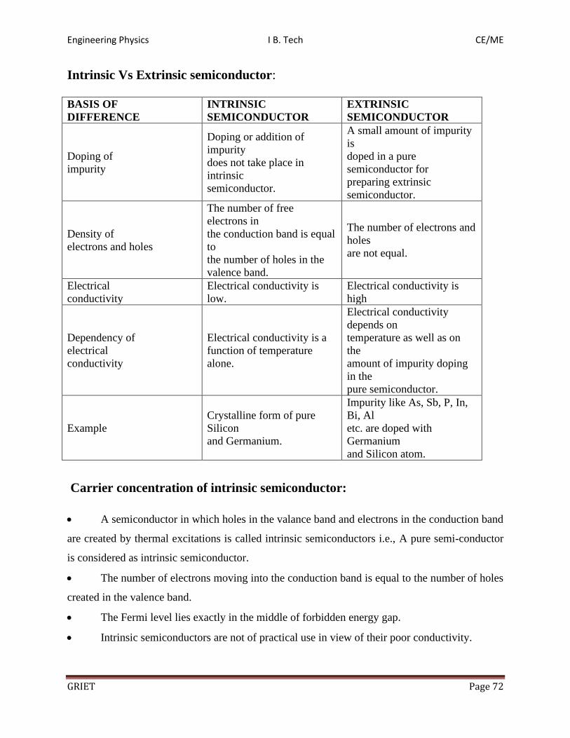
Engineering Physics I B. Tech CE/ME
GRIET Page 72
Intrinsic Vs Extrinsic semiconductor:
BASIS OF
DIFFERENCE
INTRINSIC
SEMICONDUCTOR
EXTRINSIC
SEMICONDUCTOR
Doping of
impurity
Doping or addition of
impurity
does not take place in
intrinsic
semiconductor.
A small amount of impurity
is
doped in a pure
semiconductor for
preparing extrinsic
semiconductor.
Density of
electrons and holes
The number of free
electrons in
the conduction band is equal
to
the number of holes in the
valence band.
The number of electrons and
holes
are not equal.
Electrical
conductivity
Electrical conductivity is
low.
Electrical conductivity is
high
Dependency of
electrical
conductivity
Electrical conductivity is a
function of temperature
alone.
Electrical conductivity
depends on
temperature as well as on
the
amount of impurity doping
in the
pure semiconductor.
Example
Crystalline form of pure
Silicon
and Germanium.
Impurity like As, Sb, P, In,
Bi, Al
etc. are doped with
Germanium
and Silicon atom.
Carrier concentration of intrinsic semiconductor:
• A semiconductor in which holes in the valance band and electrons in the conduction band
are created by thermal excitations is called intrinsic semiconductors i.e., A pure semi-conductor
is considered as intrinsic semiconductor.
• The number of electrons moving into the conduction band is equal to the number of holes
created in the valence band.
• The Fermi level lies exactly in the middle of forbidden energy gap.
• Intrinsic semiconductors are not of practical use in view of their poor conductivity.

Engineering Physics I B. Tech CE/ME
GRIET Page 73
Carrier concentration in intrinsic semi-conductors is given as
𝑛𝑖 = 2(2𝜋KT
ℎ²) 3/2 (𝑚𝑒
∗𝑚𝑝∗ ) ¾ exp(
−Eg
2KT)
Where, 𝑚𝑒∗ is mass of electron in conduction band
𝑚𝑝∗ is mass of hole in valence band
K is Boltzmann const. and
T is absolute temp.
n-type extrinsic semiconductor:
• When pentavalent impurities like P, As, Sb is added to the intrinsic semi-conductors,
resultant semiconductor is called n-type semi-conductor.
• The concentration of free electrons is more when compared to concentration of holes.
Carrier concentration in n-type semiconductors is given as
N = (2 𝑁𝑑)1/2(2𝜋𝑚𝑒
∗KT
ℎ²) 3/4exp(
𝐸𝑑−Ec
2KT)
• Hence the density of the electrons in the conduction band is proportional to the square
root of the donor concentration at low temperature. As higher temperature intrinsic behavior
predominates and donor concentration becomes insignificant.
p-Type extrinsic semiconductor:
• P-type semi-conductors are fabricated by addition of trivalent atoms like Al as impurity
to the intrinsic semi-conductor.
• Hence, holes are majority charge carriers and free electrons are minority charge carriers.
Carrier concentration in P type semi-conductors is given as
• p =(2Na) ½(
2𝜋𝑚ℎ∗ KT
ℎ²) 3/4exp(
𝐸𝑣−𝐸𝑎
2KT)
• Thus the density of the holes in the valance band is proportional to the square root of the
acceptor concentration at low temperature. As temperature increases intrinsic behavior
predominates and the contribution due to acceptor atoms becomes insignificant.

Engineering Physics I B. Tech CE/ME
GRIET Page 74
Direct and Indirect band gap semiconductors:
Materials for which maximum of valence band and minimum of conduction band lie for
same value of K are called direct band gap semiconductors
Example: GaAs, In P etc.
Materials for which maximum of valence band and minimum of conduction band do not
occur at same value of K are called indirect band gap materials.
Example: Si and Ge

Engineering Physics I B. Tech CE/ME
GRIET Page 75
Previous Questions:
2 Mark Questions:
1. What is Fermi level?
2. Write a short note on Bloch theorem.
3. What is E-K diagram?
4. Distinguish between intrinsic and extrinsic semiconductors.
5. Write short notes on direct and indirect band gap semiconductors.
Essay Questions:
1. Elucidate the Fermi-Dirac distribution function of electrons and discuss the effect of
temperature on the distribution.
2. Explain motion of an electron in a periodic potential using Kronig-Penney Model.
3. Distinguish between conductors, Insulator and Semiconductors
4. Write short notes on Effective Mass of an Electron.
5. Explain carrier concentrations in n-type and p-type semiconductors.
Engineering Physics I B. Tech CE/ME
GRIET Page 76
UNIT-IV
ENGINEERED SEMICONDUCTOR MATERIALS
Introduction:
Basic concepts, origin and importance of Nanotechnology
While the topic nanotechnology seems to be relatively new, the existence of functional devices
and structure of nanometer dimensions not new and in fact nanostructures exists on earth as long
as life exists.
In 4th century, roman glass makers produced cups made of soda lime glass containing silver and
gold nanoparticles. The color of the cup changes from green to deep red when light source is
placed in it.
In 18th century British scientists, Thomas wedge wood and Sir Humprey Davy were able to
provide images using silver nitrate and chloride, but their images were not permanent.
Photography which has been developed in the 19th century depends on production of silver nano
particles sensitive to light.
In 1883, the American scientist George Eastman produced a film containing a large paper strip
coated with an emulsion containing silver halides. He later developed this into a flexible film that
could be rolled which made photography very simple.
In 1960, Richard Feynman presented a lecture at a meeting of American physical society entitled
“There are plenty of room at the bottom” where he speculated on the possibility and potent of
nano sized particles.The term “Nano Technology” was defined by Tokyo Science University
professor “Norio -Taniguchi” in 1974.
Nano Scale: Nano mean 10 -9,A nanometer (nm) is one thousand millionth of a meter (10 -9 m).
Atoms are extremely small and the diameter of a single atom can vary from 0.1 to 0.5 nm
depending upon the type of element. For example, one carbon atom is approximately 0.15 nm in
diameter.
Engineering Physics I B. Tech CE/ME
GRIET Page 77
To understand how one nm is, Let us see few comparisons
A red blood cell is approximately 7000nm wide and a water molecule is almost 0.3 nm across.
Quite often people make a comparison with a human air, which is about 80000 nm wide.
Nano Science:
Nan science can be defined as the study of phenomena and manipulation of materials at atomic,
molecular and macromolecular scales, where properties differ significantly from those at a larger
scale.
Nano technology: Nano technology can be defined as the design, characterization, production
and applications of structures, devices and systems by controlling shape and size at the
nanometer scale.
Nano materials:
Nano materials could be defined as those materials which have structured components with size
less than 100nm at least in one-dimension.
Why the properties of Nano particles are different?
Two principal factors cause the properties of Nanomaterials different from other materials.
1. Quantum confinement.
2. Increase in surface area to volume ratio
Quantum confinement: The quantum confinement effect is observed when the size of the
particle is too small to be comparable to the wavelength of the electron. To understand this effect
we break the words like quantum and confinement, the word confinement means to confine the
motion of randomly moving electron to restrict its motion in specific energy levels (discreteness)
and quantum reflects the atomic realm of particles. So, as the size of a particle decrease till we a
reach a Nano scale the decrease in confining dimension makes the energy levels discrete and this
increase or widens up the band gap and ultimately the band gap energy also increases.

Engineering Physics I B. Tech CE/ME
GRIET Page 78
Increase in surface area to volume ratio:
First, Nano materials have a relatively larger surface area when compared to the same volume of
material produced in a larger (Bulk) form.
Example1: Let us consider a sphere of radius ‘r’
Its surface area = 4πr2
Itsvolume = 4/3 πr3
Surface area to volume ratio = (3/r)
Thus, when the radius of the sphere decreases, its surface area to volume ratio increases.
Example2:
Let us consider another example, for a one cube volume shown in fig (a), the surface area is 6m2.
When it is divided into eight pieces its surface area becomes 12m2.
When the same volume divided into 27 pieces its surface area becomes 18m2.
Thus we find that when the given volume is divided into smaller pieces, the surface area
increases. Hence as particle size decreases, a greater portion of atoms are found at the surface
compared to those inside. It makes materials more chemically Reactive. This affects their
strength or electrical properties.

Engineering Physics I B. Tech CE/ME
GRIET Page 79
Density of States in 2D, 1D and 0D:
The density of states function describes the number of states that are available in a system
and is essential for determining the carrier concentrations and energy distributions of
carriers within a semiconductor.
In semiconductors, the free motion of carriers is limited to two, one, and zero spatial
dimensions. When applying semiconductor statistics to systems of these dimensions,
the density of states in quantum wells (2D), quantum wires (1D), and quantum dots
(0D) must be known.
Density of States in 2D can be derived as 𝑔(𝐸)2𝐷 =𝑚∗
𝜋ℏ2
It is significant that the 2D density of states does not depend on energy. Immediately,
as the top of the energy -gap is reached, there is a significant number of available
states.
Density of States in 2D can be derived as 𝑔(𝐸)1𝐷 = 1
ℏ𝜋√
𝑚∗
2(𝐸 −𝐸𝑐)
When considering the density of states for a 0D structure no free motion is possible.
Because there is no k- space to be filled with electrons and all available states exist
only at discrete energies, we describe the density of states for 0D with the delta
function. Thus
Density of States in 0D can be derived as 𝑔(𝐸)0𝐷 = 2𝛿(𝐸 −𝐸𝑐)
Engineering Physics I B. Tech CE/ME
GRIET Page 80
Practical examples of low-dimensional systems:
There are different classifications of nanostructures in nanotechnology. Nano structures are
usually classified according to their geometrical dimensions.
There are four classes of quantum structures, namely
1. Bulk conductors (3-D)
2. Quantum wells (2-D)
3. Quantum wires (1-D)
4. Quantum Dots (0-D)
Quantum wells(2-D):
A potential well of nanometric size is known as quantum well. This well is like a cage in which
the carrier particles (i.e., the excitons) can be trapped, like light can be trapped between the
mirrors. We can create different layers of semiconductors having nanometric dimension to act as
traps foe excitons. These trapped particles can be considered to be in quantum confinement.
Due to this quantum confinement, the motion of carriers is restricted. In a quantum well, the
excitons can move freely sideways in the plane of a thin layer, but they might like to move in the
forward and backward directions as well. Due to the confinement of carriers, the structure
quantum well has important applications in making different useful devices. Quantum wells are
now widely used to make semiconductor lasers and other important devices. A quantum well is
shown in figure d.
Quantum wires(1-D): if a nanostructured material has one dimension that is outside the
nanometric size range, then it is known as quantum wires. Actually, such a shape of
nanomaterials has two dimensions in nanometric range and the third one is large. Nanostructures
have a shape like rod, and consist of nanotubes, nanorods, nanoneedles, and Nano wires. The
carriers trapped in such structures can be considered to be in 1-D quantum confinement. In this
case, an exciton is only free to choose its trajectory along the wire. However, for each motion of
its movement, the exciton can have various ways of being confined. A simple structure of a
quantum nanowire is shown in fig d.
Quantum Dots(0-D):
In the method of reducing the size of bulk material up to Nano level, an extreme case occurs
where all three dimensions of bulk are reduced to the low nanometric range. The resulting
structure is known as quantum dot. As we have discussed that a quantum well leads 2-D

Engineering Physics I B. Tech CE/ME
GRIET Page 81
quantum confinement, and by going one step ahead, in quantum wire, there is 1-D quantum
confinement. Now, we can go another step ahead, i.e., the final step, and put the exciton in 0-D
quantum confinement in just a tiny dot of a given semiconductor material [fig d]. Hence, in this
situation, the exciton only has confined states, i.e., there are no freely moving excitons. Now, it
is clear that the quantum dots behave in very different and newer ways. Although a quantum dot
has many thousands of atoms, but due to its peculiar properties, it is considered more like a
single atom rather than many atoms. Due to its specific characteristics, quantum dot system may
make the ideal laser material, which is very much focused. It may be used as a basic building
block in making a quantum computer.
Figure d
Fabrication of Nanomaterials:
• Two main approaches are used in Nano technology for fabrication of nanomaterials
• 1. Bottom up : Materials and devices are built from molecular components
which assemble chemically using principles of molecular recognition.
Example: Sol-Gel
• 2. Top down : Nano objects are constructed from larger entities without Atomic level
control.
Example: Chemical Vapor Deposition

Engineering Physics I B. Tech CE/ME
GRIET Page 82
Bottom-up and Top-down fabrication with examples:
• Materials will be fabricated by using any one of the following approaches.
• Bottom up: Materials and devices are built from molecular components which assemble
chemically using principles of molecular recognition. (Refers to build up Nano material
from bottom i.e. atom by atom, cluster by cluster)
Example: Sol-Gel process
Sol-Gel process:
• This is an example for Bottom-Up approach comes under chemical method.
• In solutions, molecules of Nanometer size are dispersed and move randomly, hence the
solutions are clear.
• In colloids, the molecules of size ranging from 20µm to 100µm are suspended in a
solvent.
• When mixed with a liquid, colloids look cloudy or even milky. A colloid that suspended
in a liquid is called a “Sol”. A suspension that keeps its shape is called a “Gel”
• Thus “Sol-Gel”s are suspensions of colloids in liquids that keep their shape.
• “Sol-Gel” formation occurs in different stages like a) Hydrolysis b) condensation
c) Growth of particles d) Agglomeration of particles.
• The rate of hydrolysis and condensation reactions are depends on various factors such as
pH, temperature, molar reaction, catalyst and process of drying.
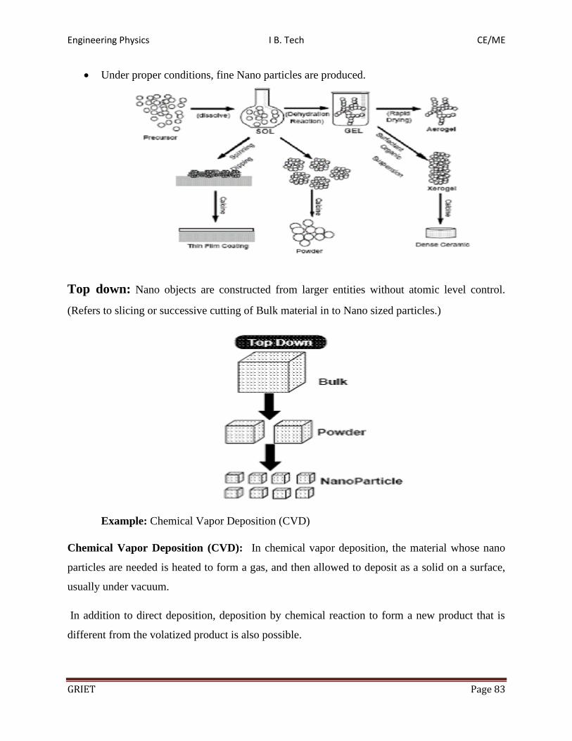
Engineering Physics I B. Tech CE/ME
GRIET Page 83
• Under proper conditions, fine Nano particles are produced.
Top down: Nano objects are constructed from larger entities without atomic level control.
(Refers to slicing or successive cutting of Bulk material in to Nano sized particles.)
Example: Chemical Vapor Deposition (CVD)
Chemical Vapor Deposition (CVD): In chemical vapor deposition, the material whose nano
particles are needed is heated to form a gas, and then allowed to deposit as a solid on a surface,
usually under vacuum.
In addition to direct deposition, deposition by chemical reaction to form a new product that is
different from the volatized product is also possible.

Engineering Physics I B. Tech CE/ME
GRIET Page 84
If vapors of carbon or oxygen are present with the metal, nano powders of carbides and oxides
can readily be obtained.
For the production of pure metal powders, microwaves tuned to the metal excitation frequencies
are used to melt and vaporize the materials to produce plasma at temperatures of the order of
1700 – 1800 K. The plasma then enters water cooled reaction column which helps the formation
of nano size particles.
After the nano particles attain appropriate cooling temperature (900 – 1000 K), they are filtered
from the exhaust gas flow and fall into a container.The factors that decide the particle grain size
are the metal concentration in the gas phase, flow rate of metal vapor, and temperature.
Chemical vapor deposition can also be used to coat surfaces by keeping the object to be coated in
the presence of the chemical vapor. The first layer of atoms or molecules deposited may not form
good coating with surface. In such a case, the deposited species can act as template on which
materials can grow. Sometimes a site for crystallization may form which may result in the
vertical growth of the structures. Usually a material is coated on a surface and then parts of the
coating are removed using a strong electron beam or chemicals. Chemical vapor deposition is
then used to build structures on these surfaces
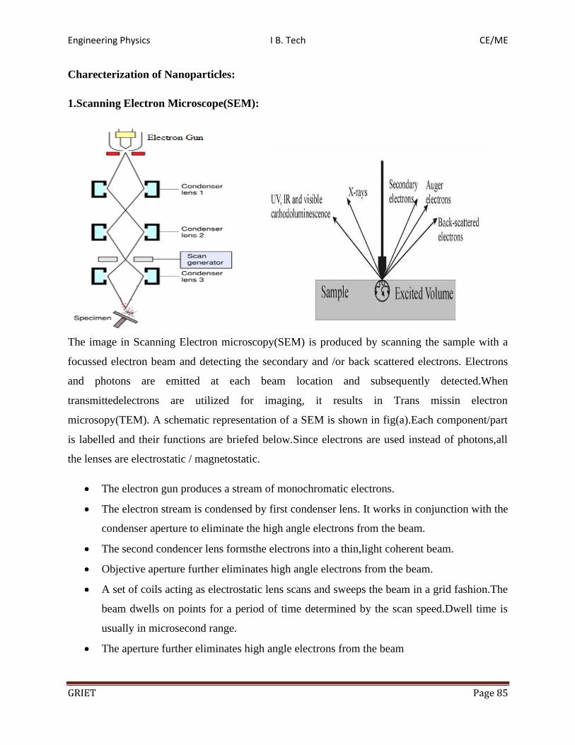
Engineering Physics I B. Tech CE/ME
GRIET Page 85
Charecterization of Nanoparticles:
1.Scanning Electron Microscope(SEM):
The image in Scanning Electron microscopy(SEM) is produced by scanning the sample with a
focussed electron beam and detecting the secondary and /or back scattered electrons. Electrons
and photons are emitted at each beam location and subsequently detected.When
transmittedelectrons are utilized for imaging, it results in Trans missin electron
microsopy(TEM). A schematic representation of a SEM is shown in fig(a).Each component/part
is labelled and their functions are briefed below.Since electrons are used instead of photons,all
the lenses are electrostatic / magnetostatic.
• The electron gun produces a stream of monochromatic electrons.
• The electron stream is condensed by first condenser lens. It works in conjunction with the
condenser aperture to eliminate the high angle electrons from the beam.
• The second condencer lens formsthe electrons into a thin,light coherent beam.
• Objective aperture further eliminates high angle electrons from the beam.
• A set of coils acting as electrostatic lens scans and sweeps the beam in a grid fashion.The
beam dwells on points for a period of time determined by the scan speed.Dwell time is
usually in microsecond range.
• The aperture further eliminates high angle electrons from the beam

Engineering Physics I B. Tech CE/ME
GRIET Page 86
• When the beam strikes the sample interaction occurs.Before the beam moves to the next
dwell point,the various instruments housed to measure various interactions count the
number of interactions and display a pixel on a CRT.The intensity of display is
determined by the interaction number.More interactions give a brighter pixel.
• This process is repeated until the grid scan is finished and then repeated. The entire
pattern can be scanned 30 times per second.
Specimen inetraction:Specimen inetraction results in salient features of an electron
microscope.When the energitic electrons strike the sample,various interactions occur.The
interactions occuring on the top side of the thick or bulk samples results in Scanning Electron
Microscope(SEM) while the interaction s occuring on the bottom side of the thin or foil sample
result in Transmission Electron Microscope(TEM).
Bulk specimen interactions used in SEM
Backscattered electrons:When an incident electron collides with an atom in the specimen
which is nearly normal to the incident path, we get backscattered electron at nearly 1800. The
intensity of backscattered electrons varies with specimen’s atomic number.Hence when
backscattered electrons are collected and imaged,higher atomic number elements. This
interaction is therefore utilized to differentiate parts of the specimen that have different average
atomic number.
Secondary electrons:When an incident electron passes very near an atom in the specimen,it may
impart some of its energy to the lower energy electron(Usually in the K- shell) resulting in
ionization of the electron in the specimen atom . This ionized electron leaves the atom with a
very small kinetic energy (~5ev) and is called secondary electrons.Each incident electron can
produce several secondary electrons. Since the emitted secondary electrons have low energy,only
the secondaries that are very near the surface (< 100nm) can leave the sample. Any change in the
topography of the sample changes the yield of the secondary electrons. Hence image formed
collecting secondary electrons gives the topography of the sample.
Augar electrons: During the emission of secondary electrons a lower energy electron is released
thus leaving a vacancy into inner shell. A higher energy electron from the same atom can fall to
the lower energy filling the vacancy. The surplus energy is released by the emission of outer
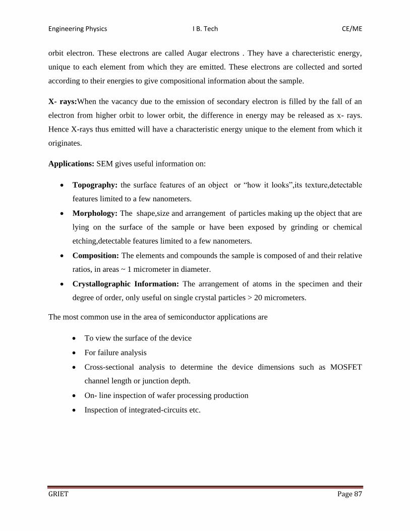
Engineering Physics I B. Tech CE/ME
GRIET Page 87
orbit electron. These electrons are called Augar electrons . They have a charecteristic energy,
unique to each element from which they are emitted. These electrons are collected and sorted
according to their energies to give compositional information about the sample.
X- rays:When the vacancy due to the emission of secondary electron is filled by the fall of an
electron from higher orbit to lower orbit, the difference in energy may be released as x- rays.
Hence X-rays thus emitted will have a characteristic energy unique to the element from which it
originates.
Applications: SEM gives useful information on:
• Topography: the surface features of an object or “how it looks”,its texture,detectable
features limited to a few nanometers.
• Morphology: The shape,size and arrangement of particles making up the object that are
lying on the surface of the sample or have been exposed by grinding or chemical
etching,detectable features limited to a few nanometers.
• Composition: The elements and compounds the sample is composed of and their relative
ratios, in areas ~ 1 micrometer in diameter.
• Crystallographic Information: The arrangement of atoms in the specimen and their
degree of order, only useful on single crystal particles > 20 micrometers.
The most common use in the area of semiconductor applications are
• To view the surface of the device
• For failure analysis
• Cross-sectional analysis to determine the device dimensions such as MOSFET
channel length or junction depth.
• On- line inspection of wafer processing production
• Inspection of integrated-circuits etc.
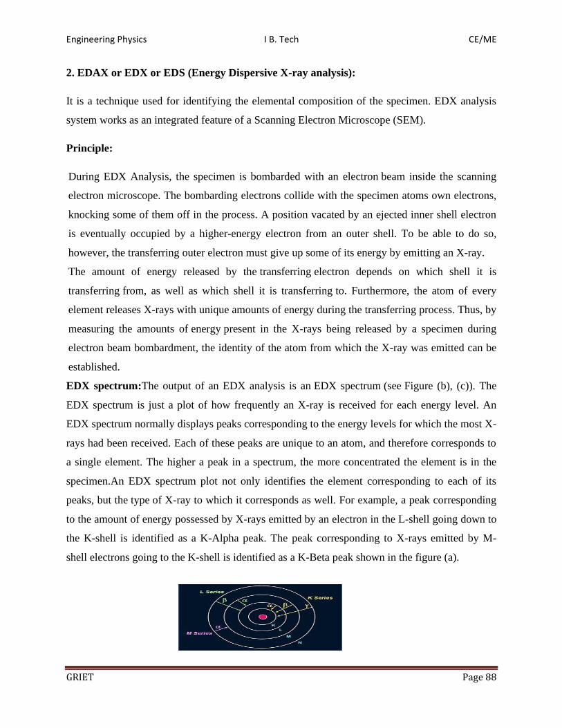
Engineering Physics I B. Tech CE/ME
GRIET Page 88
2. EDAX or EDX or EDS (Energy Dispersive X-ray analysis):
It is a technique used for identifying the elemental composition of the specimen. EDX analysis
system works as an integrated feature of a Scanning Electron Microscope (SEM).
Principle:
During EDX Analysis, the specimen is bombarded with an electron beam inside the scanning
electron microscope. The bombarding electrons collide with the specimen atoms own electrons,
knocking some of them off in the process. A position vacated by an ejected inner shell electron
is eventually occupied by a higher-energy electron from an outer shell. To be able to do so,
however, the transferring outer electron must give up some of its energy by emitting an X-ray.
The amount of energy released by the transferring electron depends on which shell it is
transferring from, as well as which shell it is transferring to. Furthermore, the atom of every
element releases X-rays with unique amounts of energy during the transferring process. Thus, by
measuring the amounts of energy present in the X-rays being released by a specimen during
electron beam bombardment, the identity of the atom from which the X-ray was emitted can be
established.
EDX spectrum:The output of an EDX analysis is an EDX spectrum (see Figure (b), (c)). The
EDX spectrum is just a plot of how frequently an X-ray is received for each energy level. An
EDX spectrum normally displays peaks corresponding to the energy levels for which the most X-
rays had been received. Each of these peaks are unique to an atom, and therefore corresponds to
a single element. The higher a peak in a spectrum, the more concentrated the element is in the
specimen.An EDX spectrum plot not only identifies the element corresponding to each of its
peaks, but the type of X-ray to which it corresponds as well. For example, a peak corresponding
to the amount of energy possessed by X-rays emitted by an electron in the L-shell going down to
the K-shell is identified as a K-Alpha peak. The peak corresponding to X-rays emitted by M-
shell electrons going to the K-shell is identified as a K-Beta peak shown in the figure (a).
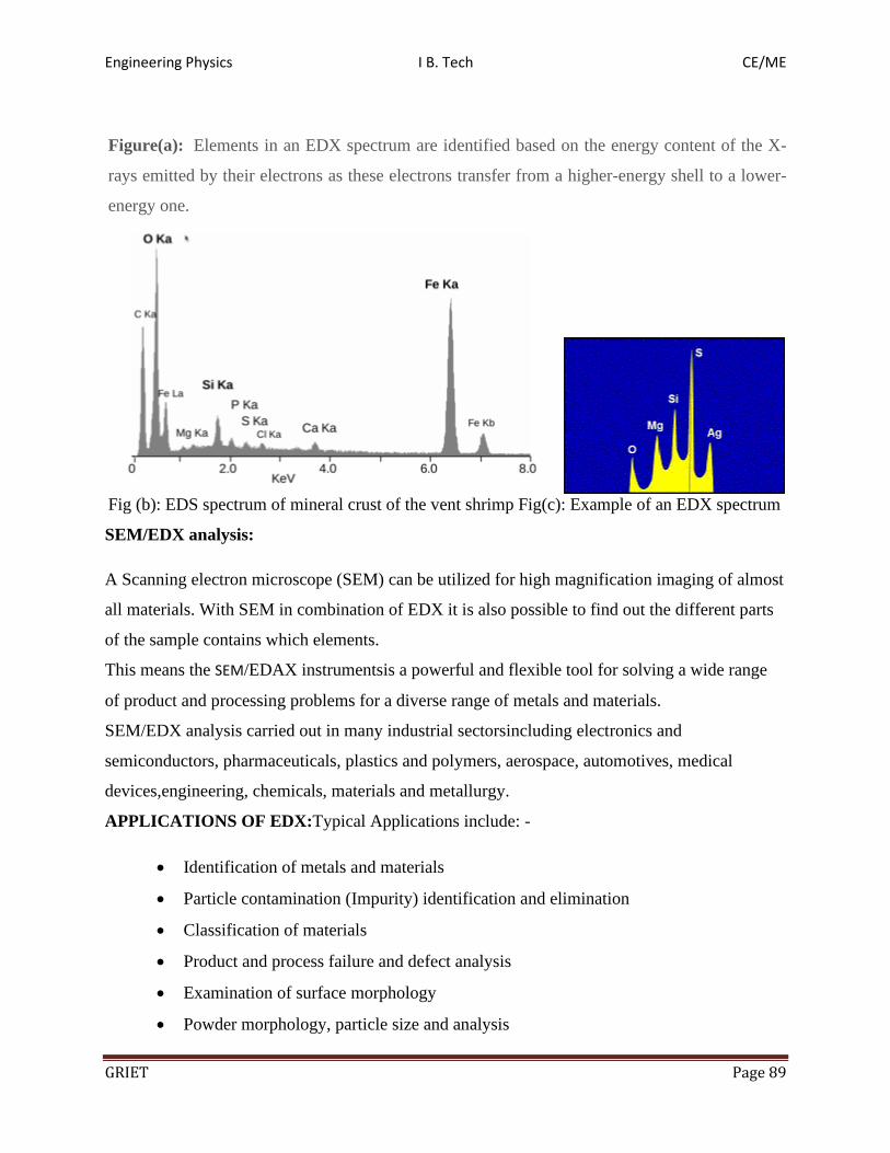
Engineering Physics I B. Tech CE/ME
GRIET Page 89
Figure(a): Elements in an EDX spectrum are identified based on the energy content of the X-
rays emitted by their electrons as these electrons transfer from a higher-energy shell to a lower-
energy one.
Fig (b): EDS spectrum of mineral crust of the vent shrimp Fig(c): Example of an EDX spectrum
SEM/EDX analysis:
A Scanning electron microscope (SEM) can be utilized for high magnification imaging of almost
all materials. With SEM in combination of EDX it is also possible to find out the different parts
of the sample contains which elements.
This means the SEM/EDAX instrumentsis a powerful and flexible tool for solving a wide range
of product and processing problems for a diverse range of metals and materials.
SEM/EDX analysis carried out in many industrial sectorsincluding electronics and
semiconductors, pharmaceuticals, plastics and polymers, aerospace, automotives, medical
devices,engineering, chemicals, materials and metallurgy.
APPLICATIONS OF EDX:Typical Applications include: -
• Identification of metals and materials
• Particle contamination (Impurity) identification and elimination
• Classification of materials
• Product and process failure and defect analysis
• Examination of surface morphology
• Powder morphology, particle size and analysis
Engineering Physics I B. Tech CE/ME
GRIET Page 90
• Cleaning problems and chemical etching
• Welding and joining technology quality evaluation and failure investigation
• Paint and coating failure and delaminating (Failure of composite materials)
investigation
• Identification and elimination of corrosion and oxidization problems
• Contamination or stain investigation
• Structural analysis
• Reverse engineering of products and processes
3. Transmission Electron Microscope (TEM):
A schematic representation of a TEM is shown in fig 1. Each component /part is labeled and
their functions are briefed below.
• The electron gun produces a stream of monochromatic electrons.
• This stream is focused to a small coherent beam by the first and second condense lenses.
• The condenser aperture knocks off high angle electrons.
• The beam strikes the specimen.
• The transmitted portion is focused by the objective lens into an image.
• Objective aperture enhances the contrast by blocking out high-angle diffracted electrons.
• Selected area aperture enables to examine the periodic diffraction of electrons by an
ordered arrangement of atoms in the sample.
• Intermediate and projector lenses enlarge the image.
• The beam strikes the phosphor screen and image is formed on the screen. The darker
areas of the image represent thicker or denser samples areas since these areas transmit
lesser electrons. The brighter areas of the image represent thinner or lesser dense sample
areas since these areas transmit more electrons.

Engineering Physics I B. Tech CE/ME
GRIET Page 91
Fig: Transmission Electron Microscope
The specimen interactions used in TEM:
Unscattered electrons:These are electrons transmitted through a thin specimen without any
interaction occurring inside the specimen. The intensity of transmitted unscattered electrons is
inversely proportional to the thickness of the specimen. Hence thicker areas of the specimen
appear darker than the thinner areas.
Elastically scattered electrons:These are electrons that are scattered by atoms in the specimen
without loss of energy. These scattered electrons are then transmitted through the remaining
portions of the specimen. The scattered electrons follow Bragg’s law 2𝑑𝑠𝑖𝑛𝜃 = 𝑛𝜆. Hence by
collecting the scattered electrons at different angles, one can get information about the
orientation, atomic arrangement and phase present.
In elastically scattered electrons:These are electrons that interact with specimen atoms in an
inelastic manner, loosing energy. Then they are transmitted through the remaining portions of the
specimen. The inelastic loss of energy is characteristic of the elements that have interacted with.
These energies are unique to bonding state of each element. Hence this can be used to extract
both compositional and bonding information.

Engineering Physics I B. Tech CE/ME
GRIET Page 92
TEM Analysis:
Fig 2: TEM image of Ag Nano particles.
A TEM image of the silver Nano particles is shown in the fig 2. The Ag Nano particles are
spherical in shape with smooth surface morphology. the diameter of the Nano particles is found
to be approximately 15 nm. TEM image also shows that the produced Nano particles are more or
less uniform in size and shape.
Applications: TEM gives the following useful information’s:
Morphology: The size, shape and arrangement of particles as well as their relationship to one
another on the scale of atomic diameters.
Crystallographic information: The arrangement of atoms in the specimen and their degree of
order, detection of atomic-scale defects a few nanometers in diameter.
Compositional information: The elements and compounds the sample is composed of and their
relative ratios.

Engineering Physics I B. Tech CE/ME
GRIET Page 93
Previous Questions
Short answer questions
1. Write about the role of surface to volume ratio in Nano technology
2. Write any two differences between bottom-up and top-down method methods
3. What are nanomaterials? Why do they exhibit different properties?
4. Briefly explain (i) Nano Materials
Additional SAQs
5. Briefly explain quantum confinement
Long answer questions:
1. Explain bottom-up and top-down methods by which nanomaterials are fabricated
2. Explain the characterization of nanomaterials using EDAX
3. Explain in detail about the Sol-gel process for the synthesis of Nano materials.
4. Explain scanning electron microscopy (SEM) for the characterization of nanomaterials
5. Discuss the chemical vapor deposition technique for the synthesis of nanomaterials
6. Explain the characterization of nanomaterials using SEM and EDAX
7. Describe any three processes by which nanomaterials are fabricated
Additional LAQs
8. Explain the characterization of nanomaterials using TEM
9. Write a short note on density of states in 2D, 1D and 0D
10. Briefly discuss practical examples of low-dimensional systems such as quantum wells, wires
and dot

Engineering Physics I B. Tech CE/ME
GRIET Page 94
UNIT-V
ACOUSTICS & ULTRASONICS
Introduction:
The branch of physics which deals with the planning of a building or a hall with a view
to provide best audible sound to the audience is called acoustics of buildings or architectural
acoustics.
Now a days sound engineering has become very important in film industry,
broadcasting and television and even in the traditional music, dance and drama. Any hall meant
for music or speech should satisfy some minimum acoustical standards apart from the standards
prescribed for accommodation, ventilation and other physical comforts like air conditioning.
An auditorium or a hall is said to be acoustically good if the following conditions are
satisfied.
Basic Requirements of Acoustically Good hall:
• The sound heard must be sufficiently loud in every part of the hall and no echoes should
be present.
• To hear good sound volume of the hall is very important that is in deciding the volume of
the hall its height is important than the length and breadth. The ratio between the ceiling
height and breadth should be 2:3.
• In deciding the volume of the hall, the following guide lines are important.
In theatres - 3.74 to 4.2 m3/seat
In lecture hall – 2.8 to 3.7 m3/seat
In music halls – 4.2 to 5.6 m3/seat
• The reverberation time should be optimum i.e.; neither too large nor too small.
• The reverberation time should be 1 to 2 sec for music and 0.5 to 1sec for speech.
• For the sake of clarity, the successive syllables spoken must be clear and distinct.
• There should be no concentration of sound in any part of the hall.
• There should be no resonance within the building.
• The hall must be full of audience.
• The boundaries should be sufficiently sound proof to exclude extra noise.
• There should be no Echelon effect i.e., if an enclosure has steps from them consists of
echoes of constant phase difference. They constitute music note which creates noise

Engineering Physics I B. Tech CE/ME
GRIET Page 95
Reverberation: The prolongation of sound inside a room/hall even after the source producing
the sound is turned off is called Reverberation.
This is due to multiple reflections from the walls, ceiling, floor another reflecting
materials present in the hall.
Reverberation Time: The duration for which the sound persists even after the source has
stopped to emit sound. Such duration of time is called Reverberation Time.
It is defined as the time required for the sound to reduce its intensity to 1/106 of its
initial volume, just before the source is cut off.
It is expressed in terms of dB(decibels)
The reverberation time depends on volume of the room and absorption co efficient.
Sabine’s formula for Reverberation time:
According to Sabine’s law, the reverberation time T in seconds (the time taken by the
intensity of sound to fall to one millionth 10-6 of its original value after the source of sound is cut
off) is expressed as
T= 0.165V/A = 0.165V
ƩaS ………. (1)
Where V is the volume of the hall in m3 and ƩaS is given by
ƩaS = a1S1+ a2S2+ …..+ anSn
Here a1, a2, a3, ……. an are the absorption coefficient of the materials in the hall whose surface
areas exposed to sound are S1, S2, S3........ Sn respectively measured in m2.
From the eqn(1),
• Reverberation time (T) is directly proportional to volume of room/hall.
• Reverberation time (T) is inversely proportional to the area of sound absorbing material.
• Experimentally found that the reverberation time of 1.03secs is most suitable for all
rooms having volume less than 350 cubic meters(350m3 )
Measurement of absorption coefficient of a material:
Different materials absorb sound energy differently than the absorption of all materials is
expressed in terms of absorption coefficients (a).
• It is defined as the ratio of the sound energy absorbed by the surface to that of total sound
energy incident on the surface.
i.e.; a = sound energy absorbed by the surface
Total sound energy incident on the surface
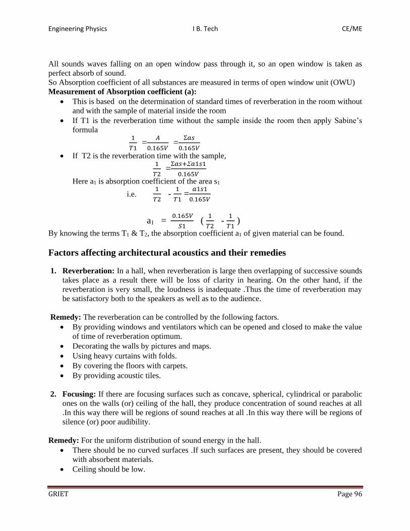
Engineering Physics I B. Tech CE/ME
GRIET Page 96
All sounds waves falling on an open window pass through it, so an open window is taken as
perfect absorb of sound.
So Absorption coefficient of all substances are measured in terms of open window unit (OWU)
Measurement of Absorption coefficient (a):
• This is based on the determination of standard times of reverberation in the room without
and with the sample of material inside the room
• If T1 is the reverberation time without the sample inside the room then apply Sabine’s
formula
1
𝑇1 =
𝐴
0.165𝑉 =
Ʃ𝑎𝑠
0.165𝑉
• If T2 is the reverberation time with the sample,
1
𝑇2 =
Ʃ𝑎𝑠+Ʃ𝑎1𝑠1
0.165𝑉
Here a1 is absorption coefficient of the area s1
i.e. 1
𝑇2 -
1
𝑇1 =
𝑎1𝑠1
0.165𝑉
a1 = 0.165𝑉
𝑆1 (
1
𝑇2 -
1
𝑇1 )
By knowing the terms T1 & T2, the absorption coefficient a1 of given material can be found.
Factors affecting architectural acoustics and their remedies
1. Reverberation: In a hall, when reverberation is large then overlapping of successive sounds
takes place as a result there will be loss of clarity in hearing. On the other hand, if the
reverberation is very small, the loudness is inadequate .Thus the time of reverberation may
be satisfactory both to the speakers as well as to the audience.
Remedy: The reverberation can be controlled by the following factors.
• By providing windows and ventilators which can be opened and closed to make the value
of time of reverberation optimum.
• Decorating the walls by pictures and maps.
• Using heavy curtains with folds.
• By covering the floors with carpets.
• By providing acoustic tiles.
2. Focusing: If there are focusing surfaces such as concave, spherical, cylindrical or parabolic
ones on the walls (or) ceiling of the hall, they produce concentration of sound reaches at all
.In this way there will be regions of sound reaches at all .In this way there will be regions of
silence (or) poor audibility.
Remedy: For the uniform distribution of sound energy in the hall.
• There should be no curved surfaces .If such surfaces are present, they should be covered
with absorbent materials.
• Ceiling should be low.

Engineering Physics I B. Tech CE/ME
GRIET Page 97
• A parabolic reflected surface arranged with the speaker at the focus is also helpful in
sending beam of sound in the hall.
3. Echoes: In small halls, the walls of the hall will scatter the sound waves rather than
reflecting it, this creates nuisance effect due to echoes. The echoes are formed when the time
interval between the direct and reflected sound waves are about 1/15 th of a second .This
effect occurs due to the reason that the reflected sound waves reaches the observer later than
the direct sound.
Remedy: Echoes can be avoided by lining the surfaces with suitable sound absorbing materials
and by providing enough no. of doors and windows.
4. Echelon Effect: If there is a regular repetition of echoes of original sound to the observer then
the effect is called Echelon effect.
E.g.: Sound produced from equally spaced steps in stair case at regular intervals produces
echelon effect.
Remedy: This can be avoided by covering the surface by proper sound absorbing materials.
4. Loudness: It is the degree of sensation produced on the ear, it varies from one place to
another place in the same auditorium .This defect is caused due to bad acoustical
construction of buildings. The loudness will be very low in some area and be very high in
some areas can be optimized by the following remedies.
Remedies:
• Loud speakers should be placed where we have low loudness.
• The loudness can also be increased by making reflecting surfaces wherever necessary.
• Loudness can be increased by constructing low ceiling.
• Absorbents should be placed at the places where we have high loudness.
• By adopting the above remedies loudness should be made even, all overt the auditorium.
6. Noise:
Any unwanted sound is called noise. Generally arise due to airborne noise, Structure borne noise
and inside noise
Remedies:
• By placing sound proof agents.
• By placing sound insulation.

Engineering Physics I B. Tech CE/ME
GRIET Page 98
Ultrasonics
Introduction
We all know that sound is due to vibrations of one or the other kind of particles.
Sound waves can be classified under three categories acc. to their frequency. They are
infrasonic waves, audible waves and ultrasonic waves. Longitudinal waves having
frequencies below 20Hz are called infrasonic or subsonic waves, which can’t be heard by
human beings. They are produced by very big vibrators such as the waves produced in
earthquakes etc. Infrasonic waves can be heard by snakes.
Longitudinal waves having frequencies lying between 20Hz to 20KHz are called
audible waves. Audible waves are produced by vibrating bodies such as vocal cords
(human and animal voices), stretched strings (violin, guitar), motion of doors and trees
etc. Those audible waves which are produced by regular periodic vibrations of definite
frequency have a pleasing effect on the ears of human beings and are called musical
sounds, while those waves which are produced by irregular non periodic disturbances of
bodies produce an irritating effect on the ears and are called noise waves. Longitudinal
waves having frequencies above 20KHz are called ultrasonic waves. They are produced
and heard by bats. Ultrasonic waves can be produced by crystal oscillators in laboratory.
Ultrasonic waves are also called supersonic waves.
Classification of Ultrasonic waves
Ultrasonic waves are classified into four categories based on the mode of propagation
of the particle in the medium, with respect to the direction of propagation of the initial waves.
They are as given below
i) Longitudinal waves
ii) Transverse or shear waves
iii) Surface or Rayleigh waves, and
iv) Plate or Lamb waves.
i) Longitudinal or Compressional or Pressure Ultrasonic Waves:
In the longitudinal waves particles of medium vibrate back and forth parallel to
the direction of propagation of wave. Due to the vibrations of the particles, alternate
compression and rarefaction zones are produced, as shown in fig.
The resulting wave is called longitudinal ultrasonic wave or compressional
wave. During the particle motion in the material, compressive and dilative forces are
acting and therefore these waves are known as dilational or pressure waves.
Longitudinal waves can be propagated in solids, liquids and gases. They are easy to
generate, detect and also to convert into other modes of vibrations.
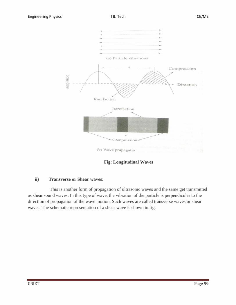
Engineering Physics I B. Tech CE/ME
GRIET Page 99
Fig: Longitudinal Waves
ii) Transverse or Shear waves:
This is another form of propagation of ultrasonic waves and the same get transmitted
as shear sound waves. In this type of wave, the vibration of the particle is perpendicular to the
direction of propagation of the wave motion. Such waves are called transverse waves or shear
waves. The schematic representation of a shear wave is shown in fig.

Engineering Physics I B. Tech CE/ME
GRIET Page 100
Fig: Transverse Waves
The velocity of the shear waves is half of the longitudinal waves in the same material.
When a wave travels through a material, it makes the particles of the material vibrate due to the
transfer of energy. The vibrating particles make the neighbouring particles vibrate. This results in
reduction of energy of the ultrasonic wave and hence, velocity of the shear wave is half the
longitudinal waves. Shear waves can be passed only through solids. They cannot be generated in
liquids or gases.
iii) Surface or Rayleigh waves:
The surface waves travel along the flat or curved surface of thick solids without
influencing the bulk of medium below the surface. The depth to which these waves propagate
below the surface with considerable intensity is approximately equal to wavelength of the wave.
Practically all of its energy is attenuated within this depth. Surface waves are analogous to the
water waves. In water waves, the motion of the particle is both transverse and longitudinal in a
plane containing the direction of propagation and is also normal to the surface. These waves are
used to detect cracks or flaws on or near the surface of test objects. During the propagation of
surface waves, the particles of medium describe elliptical orbits as shown in fig.
Fig: Surface Waves
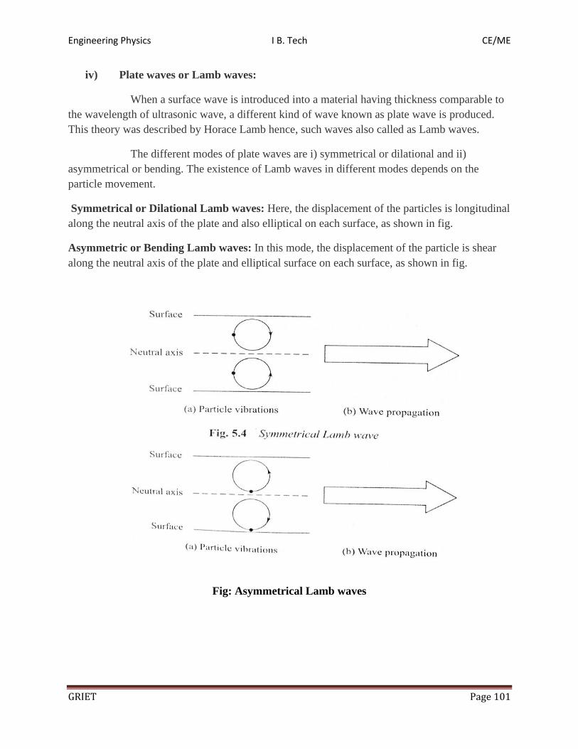
Engineering Physics I B. Tech CE/ME
GRIET Page 101
iv) Plate waves or Lamb waves:
When a surface wave is introduced into a material having thickness comparable to
the wavelength of ultrasonic wave, a different kind of wave known as plate wave is produced.
This theory was described by Horace Lamb hence, such waves also called as Lamb waves.
The different modes of plate waves are i) symmetrical or dilational and ii)
asymmetrical or bending. The existence of Lamb waves in different modes depends on the
particle movement.
Symmetrical or Dilational Lamb waves: Here, the displacement of the particles is longitudinal
along the neutral axis of the plate and also elliptical on each surface, as shown in fig.
Asymmetric or Bending Lamb waves: In this mode, the displacement of the particle is shear
along the neutral axis of the plate and elliptical surface on each surface, as shown in fig.
Fig: Asymmetrical Lamb waves

Engineering Physics I B. Tech CE/ME
GRIET Page 102
Production of ultrasonic waves:
Ultrasonic waves are produced by the following methods.
i) Piezo-electric generator or oscillator
ii) Magneto-striction generator or oscillator
Piezo-electric generator or oscillator:
This method is based on piezo electric effect i.e., If mechanical pressure is applied to one pair of
opposite faces of certain crystals like quartz equal and opposite electrical charges appear across
its other faces. This is called as piezo-electric effect.
The converse of piezo electric effect is also true.
If an electric field is applied to one pair of faces, the corresponding changes in the dimensions of
the other pair of faces of the crystal are produced. This is known as inverse piezo electric effect
or electrostriction.
Construction:
• The quartz crystal is placed between two metal plates A and B.
• The plates are connected to the primary (L3) of a transformer which is inductively
coupled to the electronics oscillator.
• The electronic oscillator circuit is a base tuned oscillator circuit.
• The coils L1 and L2 of oscillator circuit are taken from the secondary of a transformer T.
• The collector coil L2 is inductively coupled to base coil L1.
• The coil L1 and variable capacitor C1 form the tank circuit of the oscillator.
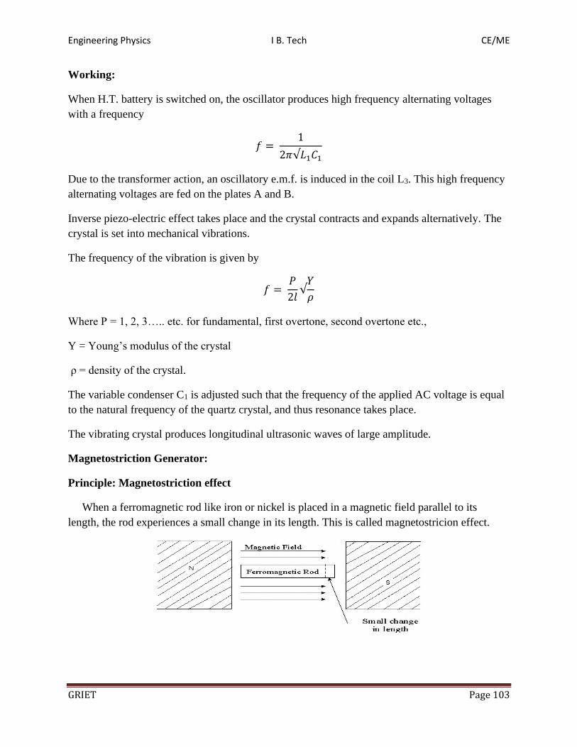
Engineering Physics I B. Tech CE/ME
GRIET Page 103
Working:
When H.T. battery is switched on, the oscillator produces high frequency alternating voltages
with a frequency
𝑓 = 1
2𝜋√𝐿1𝐶1
Due to the transformer action, an oscillatory e.m.f. is induced in the coil L3. This high frequency
alternating voltages are fed on the plates A and B.
Inverse piezo-electric effect takes place and the crystal contracts and expands alternatively. The
crystal is set into mechanical vibrations.
The frequency of the vibration is given by
𝑓 = 𝑃
2𝑙√
𝑌
𝜌
Where P = 1, 2, 3….. etc. for fundamental, first overtone, second overtone etc.,
Y = Young’s modulus of the crystal
ρ = density of the crystal.
The variable condenser C1 is adjusted such that the frequency of the applied AC voltage is equal
to the natural frequency of the quartz crystal, and thus resonance takes place.
The vibrating crystal produces longitudinal ultrasonic waves of large amplitude.
Magnetostriction Generator:
Principle: Magnetostriction effect
When a ferromagnetic rod like iron or nickel is placed in a magnetic field parallel to its
length, the rod experiences a small change in its length. This is called magnetostricion effect.

Engineering Physics I B. Tech CE/ME
GRIET Page 104
The change in length (increase or decrease) produced in the rod depends upon the strength of the
magnetic field, the nature of the materials and is independent of the direction of the magnetic
field applied.
Construction:
• XY is a rod of ferromagnetic materials like iron or nickel. The rod is clamped in the
middle.
• The alternating magnetic field is generated by electronic oscillator.
• The coil L1 wound on the right hand portion of the rod along with a variable capacitor C.
• This forms the resonant circuit of the collector tuned oscillator. The frequency of
oscillator is controlled by the variable capacitor.
• The coil L2 wound on the left hand portion of the rod is connected to the base circuit.
The coil L2 acts as feed –back loop.
Working:
When High Tension (H.T) battery is switched on, the collector circuit oscillates with a
frequency,
𝑓 = 1
2𝜋√𝐿1𝐶
This alternating current flowing through the coil L1 produces an alternating magnetic field along
the length of the rod. The result is that the rod starts vibrating due to magnetostrictive effect.
The frequency of vibration of the rod is given by
𝑓 = 1
2𝑙√
𝑌
𝜌

Engineering Physics I B. Tech CE/ME
GRIET Page 105
Where l = length of the rod
Y = Young’s modulus of the rod material and
= density of rod material
The capacitor C is adjusted so that the frequency of the oscillatory circuit is equal to natural
frequency of the rod and thus resonance takes plate.
Now the rod vibrates longitudinally with maximum amplitude and generates ultrasonic waves of
high frequency from its ends.
Properties of ultrasonic waves:
• Ultrasonic waves are having frequencies higher than 20 KHz and hence they are
highly energetic and their wavelengths are small.
• Due to their small wavelengths, the diffraction is negligible. Hence, they can be
transmitted over a long distances without any appreciable loss of energy.
• When they are passing through a medium, at discontinuities, they are partially
reflected and this property is used in Non-Destructive Technique (NDT).
• When the ultrasonic wave is absorbed by a medium, it generates heat.
• They are able to drill and cut thin metals.
• At room temperature, ultrasonic welding is possible
• The mix molten metals of widely different densities to produce alloys of uniform
composition
• Using ultrasonic wave, acoustic grating can be formed in a liquid.
Applications of ultrasonics:
SONAR: (Sound Navigation and Ranging)
• This is used to find out depth of sea and to establish communication between ships.
• In this, a beam of ultrasonic wave is directed towards the bottom of sea from where it
reflected back to a receiver. The time interval between sending and receiving the waves‘t’
is determined. Since the ultrasonic velocity ‘v’ in sea water is known, the depth of sea is
calculated as
• The depth of sea (distance between surface and bottom of the sea) = 𝑣𝑡
2
• The same procedure is used to find out the distance of the submarine or iceberg from the
surface the sea and the distance between two slips in the sea.
NDT (Pulse echo method):
Ultrasonic Testing (UT) uses high frequency sound waves (typically in the range between 0.5
and 15 MHz) to conduct examinations and make measurements. Besides its wide use in
engineering applications (such as flaw detection/evaluation, dimensional measurements, material

Engineering Physics I B. Tech CE/ME
GRIET Page 106
characterization, etc.), ultrasonic are also used in the medical field (such as sonography,
therapeutic ultrasound, etc.).
In general, ultrasonic testing is based on the capture and quantification of either the reflected
waves (pulse-echo).
Pulse-Echo System: This method is based on the principle of reflection of ultrasonic waves.
The pulse echo method may use either a single crystal unit or two crystal units. In single
transducer method, only one probe is used which acts both as transmitter and receiver (fig a).
The ultrasonic beam is incident normally on the surface of the specimen under test. The beam
travels through the specimen and is reflected back from rear surface of the specimen. If a defect
is present in its path, part of the energy will be reflected back from the defect and remaining part
travels forward in the material. The initial pulse, the echo pulse reflected from the defect and the
echo pulse reflected from the opposite face of the specimen are displayed on a CRO screen as
shown in fig b. Since the pips on the oscilloscope screen measure the elapsed time between
reflection of the pulse from the front and back surfaces, the distance between the pips is a
measure of the thickness of the specimen (fig b). The location of a defect may therefore be
accurately determined from the pips on the screen.
Previous Questions
2 Mark Questions:
1) Write a note on piezoelectricity?
2) Define reverberation and reverberation time?
3) Mention applications of ultrasonic waves in any two fields?
Essay Questions:
1) a. Explain a method to calculate the Absorption Coefficient of a material?
b. Derive the expression of Sabine’s formula of Reverberation time?
2) a. What is Acoustic Quieting and discuss various aspects Acoustic Quieting?
3) a. Discuss the factors affecting the architectural acoustics and their remedies?

Engineering Physics I B. Tech CE/ME
GRIET Page 107
b. Explain some basic requirements of acoustically good hall?
4) a. What are the factors affecting the architectural acoustics and explain the remedies?
b. Discuss different types of ultrasonic production systems?
5) a.What are the basic requirements of acoustically good hall and explain how these
requirements can be achieved?
b. Describe the production of ultrasonic waves by Magnetostriction method?


