
2013.04 Ver. G Copyright Grenergy OPTO, Inc. www.grenergy-ic.com 1
Preliminary GR8875N Series
Features � High-Voltage (700V) Startup Circuit
� Very Low Startup Current (<30uA)
� Under-Voltage Lockout (UVLO)
� 100mW Standby Power
� Non-Audible-Noise Green-Mode Control
� 65KHz Switching Frequency with Jittering for
Reducing EMI
� Cycle-by-Cycle Peak Current Limiting
� Internal Leading-Edge Blanking
� Internal Slope Compensation
� Gate Output Maximum Voltage Clamp
� Internal 6mS Soft Start
� Soft Driving for Reducing EMI
� AC Input Brownout Protection with Hysteresis
� Programmable Over Temperature Latch (OTP)
Function
� Over-Voltage Protection (OVP) on VCC pin
� Over-Load Protection (OLP)
� Flexible Latch Shutdown Combination: OVP;
OVP+OTP
� 500mA Driving Capability
� SOP-8 /SOP-7/DIP-8 Green Package
Applications
� Adaptor/ Open Frame Power Supply
� LCD Monitor/TV Power Supply
Description
The GR8875N series is a highly-integrated, low
startup current, current mode PWM controller with
green-mode function, high-voltage start up circuit,
and provides several protections such as OLP, OVP,
and OCP for fault conditions. A high-voltage current
source supplies the start up current and the
traditional start up resistance can be saved in order
to reduce the start up power loss. The controller
also includes the leading-edge blanking of the
current sensing, internal slope compensation and
cycle-by-cycle peak current limiting. It is also
integrated soft driving for reducing EMI, gate output
voltage clamp function for protecting power
MOSFET.
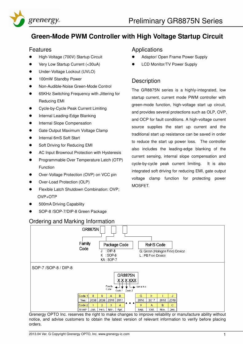
Ordering and Marking Information
SOP-7 /SOP-8 / DIP-8
Code 1 8 9 A B G H I J Year 2008 2009 2010 2011 2016 2017 2018 2019 Code 2 1 2 3 4 9 A B C Month Jan. Feb. Mar. Apr. ● ● ● Sep. Oct. Nov. Dec. Grenergy OPTO Inc. reserves the right to make changes to improve reliability or manufacture ability without
notice, and advise customers to obtain the latest version of relevant information to verify before placing
orders.
Green-Mode PWM Controller with High Voltage Startup Circuit
2013.04 Ver. G Copyright Grenergy OPTO, Inc. www.grenergy-ic.com 2
Preliminary GR8875N Series
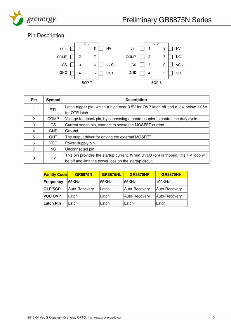
Pin Description
Pin Symbol Description
1 RTL Latch trigger pin, which a high over 3.5V for OVP latch off and a low below 1.05V
for OTP latch
2 COMP Voltage feedback pin, by connecting a photo-coupler to control the duty cycle.
3 CS Current sense pin, connect to sense the MOSFET current
4 GND Ground
5 OUT The output driver for driving the external MOSFET
6 VCC Power supply pin
7 NC Unconnected pin
8 HV This pin provides the startup current. When UVLO (on) is tripped, this HV loop will
be off and limit the power loss on the startup circuit.
Family Code GR8875N GR8875NL GR8875NR GR8875NH
Frequency 65KHz 65KHz 65KHz 100KHz
OLP/SCP Auto-Recovery Latch Auto-Recovery Auto-Recovery
VCC OVP Latch Latch Auto-Recovery Auto-Recovery
Latch Pin Latch Latch Latch Latch
2013.04 Ver. G Copyright Grenergy OPTO, Inc. www.grenergy-ic.com 3
Preliminary GR8875N Series
Absolute Maximum Ratings
Supply Voltage VCC --------------------------------------------------------------------------------------------------------- 30V
High-Voltage Pin, HV --------------------------------------------------------------------------------------------- - 0.3 ~ 500V
COMP, RTL, CS ------------------------------------------------------------------------------------------------------- -0.3 ~ 7V
Junction Temperature ---------------------------------------------------------------------------------------------------- 150℃
Operating Ambient Temperature ----------------------------------------------------------------------------- -40℃ ~ 85℃
Storage Temperature Range --------------------------------------------------------------------------------- -65℃ ~ 150℃
SOP-8/SOP-7 Package Thermal Resistance -------------------------------------------------------------------- 160℃/W
DIP-8 Package Thermal Resistance ------------------------------------------------------------------------------ 100℃/W
Power Dissipation (SOP-8, at ambient temperature = 85 )℃ ------------------------------------------------ 400 mW
Power Dissipation (DIP-8, at ambient temperature = 85 )℃ --------------------------------------------------- 650mW
Lead Temperature (SOP-8 & DIP-8, soldering, 10sec) ------------------------------------------------------- 230℃
Lead Temperature (All Pb free packages, soldering, 10sec) ------------------------------------------------ 260℃
ESD Voltage Protection, Human Body Model (Except HV pin) ------------------------------------------------ 3KV
ESD Voltage Protection, Machine Model ---------------------------------------------------------------------------- 300V

2013.04 Ver. G Copyright Grenergy OPTO, Inc. www.grenergy-ic.com 4
Preliminary GR8875N Series
RLT
+
-
+
-
3.5V
1.05V
Vbias
100uAOVP
OTP
Driver stage
LatchProtect
Re-startProtect
LEB
S
QR
++++
----
+
-Vcs-H/L
OCP
Vbias
OSC
Slope compensation
CS
PG EN
COMP
Soft
start
Internal Bias & Vref
VCC OK
All Blocks17V/9V
UVLO
VCC
28V
3.5VOLP
+
-
PG
+
-
Vref OK
VCC
VCC OVP
RTLLatch
GND
OLP RTLLatch
VCC OVP
HVHV Start-up
VCC
Brown in/out detect
Vcs-H/L Adiustment
BNO
BNO
OUT
NC
COMP
Vcs-H/L
Block Diagram

2013.04 Ver. G Copyright Grenergy OPTO, Inc. www.grenergy-ic.com 5
Preliminary GR8875N Series
Electrical Characteristics (TA = + 25℃, Vcc = 15.0V, unless otherwise specified)
Parameter Pin Min Typ Max Unit
HIGH-VOLTAGE SUPPLY (HV Pin)
High-Voltage Current Source (VDC=370 ,R=125k Vcc = 0V) 8 2.96 4 mA
Off-State Leakage Current 8 36 uA
Brownout Threshold (see below equation 1) DC source R=125KΩ 92 102 112 V
Brownin Threshold (see below equation 2) DC source
R=125KΩ 104 114 124 V
PWM Turn-Off Debounce Time- Normal Operation 75 mS
SUPPLY VOLTAGE
Startup Current 6 30 uA
Operating Current (with 1nF load on OUT pin), Vcomp = 0V 6 0.8 mA
Operating Current (with 1nF load on OUT pin), Vcomp = 2.5V 6 2.2 mA
Operating Current (with 1nF load on OUT pin), Protection Tripped
(OLP, OVP) 6 0.5 mA
UVLO (off) 6 8 9 10 V
UVLO (on) 6 16 17 18 V
OVP on VCC Pin 6 27 28 29 V
VOLTAGE FEEDBACK
Open Loop Voltage, Comp Pin Open 2 4.5 V
Delay Time of Comp Pin Open Loop Protection 2 50 mS
CURRENT SENSING
Current Limit @ Low Line(Vac=86V) VDC=122 Series RHV=125k to
HV Vcs-H 3 0.80 0.85 0.90 V
Current limit @ High Line(Vac=259V)VDC=366 Series RHV=125k to
HV Vcs-L 3 0.7 V
Leading-Edge Blanking Time without Tpd 3 250 nS
Input Impedance 3 1 mΩ
Delay to Output 3 100 nS
OSCILLATOR
Normal PWM Frequency 60 65 70 KHz Frequency
Jitter Range ±6% KHz
Green Mode Frequency 22 KHz
Temp. Stability (-40°C ~ 105°C) 5 %
Voltage Stability (VCC = 11V ~ 25V) 2 %
GATE DRIVER OUTPUT
Output Low Level, VCC = 15V, IO = 20mA 5 1 V
Output High Level, VCC = 15V, IO =20mA 5 8 V

2013.04 Ver. G Copyright Grenergy OPTO, Inc. www.grenergy-ic.com 6
Preliminary GR8875N Series
Rising Time, Load Capacitance = 1000pF 5 150 nS
Falling Time, Load Capacitance = 1000pF 5 50 nS
VGATE-Clamp (VCC = 25V ) 5 11 13 15 V
PWM SECTION
Maximum Duty Cycle 70 75 80 %
Soft Start Time (Freq=65kHz) 6 mS
*Latch PIN FUNCTION OPTION (See below Fig.1)
Over Voltage Protection Threshold Voltage 3 3.2 3.5 3.8 V
OVP Debounce, Fs = 65kHz 3 100 uS
Over Temperature Protection Threshold Voltage 3 0.95 1.05 1.15 V
OTP Debounce, Fs = 65kHz 3 100 uS
Output Current from RTL Pin 3 92 100 108 uA
Clamped Voltage 3 2.2 V
VCC De-latch Voltage 3.4 V
Below equations are for reference only.
Equation 1:
Equation 2:
2
]1
190[
)( K
KRHVv.
RMSonVac
+×
=−
2
1
180
)(
]K
KRHVv.[
RMSoffVac
+×
=−
2013.04 Ver. G Copyright Grenergy OPTO, Inc. www.grenergy-ic.com 7
Preliminary GR8875N Series
Application Information
Overview
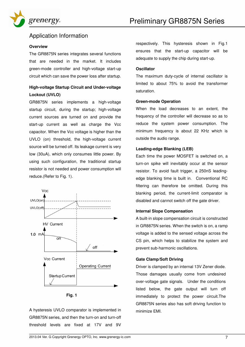
The GR8875N series integrates several functions
that are needed in the market. It includes
green-mode controller and high-voltage start-up
circuit which can save the power loss after startup.
High-voltage Startup Circuit and Under-voltage
Lockout (UVLO)
GR8875N series implements a high-voltage
startup circuit, during the startup; high-voltage
current sources are turned on and provide the
start-up current as well as charge the Vcc
capacitor. When the Vcc voltage is higher than the
UVLO (on) threshold, the high-voltage current
source will be turned off. Its leakage current is very
low (30uA), which only consumes little power. By
using such configuration, the traditional startup
resistor is not needed and power consumption will
reduce.(Refer to Fig. 1).
Fig. 1
A hysteresis UVLO comparator is implemented in
GR8875N series, and then the turn-on and turn-off
threshold levels are fixed at 17V and 9V
respectively. This hysteresis shown in Fig.1
ensures that the start-up capacitor will be
adequate to supply the chip during start-up.
Oscillator
The maximum duty-cycle of internal oscillator is
limited to about 75% to avoid the transformer
saturation.
Green-mode Operation
When the load decreases to an extent, the
frequency of the controller will decrease so as to
reduce the system power consumption. The
minimum frequency is about 22 KHz which is
outside the audio range.
Leading-edge Blanking (LEB)
Each time the power MOSFET is switched on, a
turn-on spike will inevitably occur at the sensor
resistor. To avoid fault trigger, a 250nS leading-
edge blanking time is built in. Conventional RC
filtering can therefore be omitted. During this
blanking period, the current-limit comparator is
disabled and cannot switch off the gate driver.
Internal Slope Compensation
A built-in slope compensation circuit is constructed
in GR8875N series. When the switch is on, a ramp
voltage is added to the sensed voltage across the
CS pin, which helps to stabilize the system and
prevent sub-harmonic oscillations.
Gate Clamp/Soft Driving
Driver is clamped by an internal 13V Zener diode.
Those damages usually come from undesired
over-voltage gate signals. Under the conditions
listed below, the gate output will turn off
immediately to protect the power circuit.The
GR8875N series also has soft driving function to
minimize EMI.

2013.04 Ver. G Copyright Grenergy OPTO, Inc. www.grenergy-ic.com 8
Preliminary GR8875N Series
Soft Start
During initial power on, the GR8875N series
provides soft start function. It effectively
suppresses the start up peak current to reduce the
power MOSFET drain voltage especially at high
line.
Over-load Protection (OLP)
The controller has an over load protection function.
An internal circuit detects the Comp pin level,
when the level is larger than a threshold and the
condition lasts more than 50mS, then the gate
output will keep low level. The VCC will decrease
to UVLO off level and the controller will be reset
again. Fig.2 shows the waveform of the OLP
operation.
VCC
UVLO(on)
UVLO(off)
t
t
COMP
OLP
3.5 V
t
OUT
OLP delay time
Switching SwitchingNon - Switching
OLP trip Level
(off )OLP Counter Reset
Fig. 2
Over-voltage Protection on VCC-Latch Mode
To prevent power MOSFET from being damaged,
the GR8875N series is implemented an OVP
function on VCC. When the VCC voltage is higher
than the OVP threshold voltage, the output gate
driver circuit will be shut down immediately to stop
the switching of power MOSFET. The VCC pin
OVP function is a latch type protection.GR8875N
series is working in latch mode as shown in
Fig. 3.
Fig. 3
Brown-in/Brown-out and Constant Power
Limited by HV pin
Unlike previous PWM controllers, the HV pin of
GR8875N series isn't only used for startup; it can
also detect the AC line voltage to perform
brown-in/brown-out function and set the high low
line constant power compensation. Equations 1
and 2 can be used to calculate out the level of
brown-in and brown-out converted to RMS value.
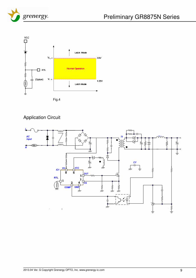
RTL Pin Latch Off Mode
The typical application for RTL pin is shown in
Fig.4. The Zener diode is setting as external OVP
protection and the NTC thermistor is setting as
external OTP protection. In the RTL pin, there are
two comparators for latch-off mode protection.
While the voltage on this pin is higher than 3.5V or
lower than 1.05V, the GR8875N series will shut
down after the de-bounce time 100uS. And the
GR8875N series will never auto recovery, unless
the VCC pin voltage is down to reset level as same
as shown in Fig. 3
2013.04 Ver. G Copyright Grenergy OPTO, Inc. www.grenergy-ic.com 9
Preliminary GR8875N Series
Fig.4
Application Circuit
RTL

2013.04 Ver. G Copyright Grenergy OPTO, Inc. www.grenergy-ic.com 10
Preliminary GR8875N Series
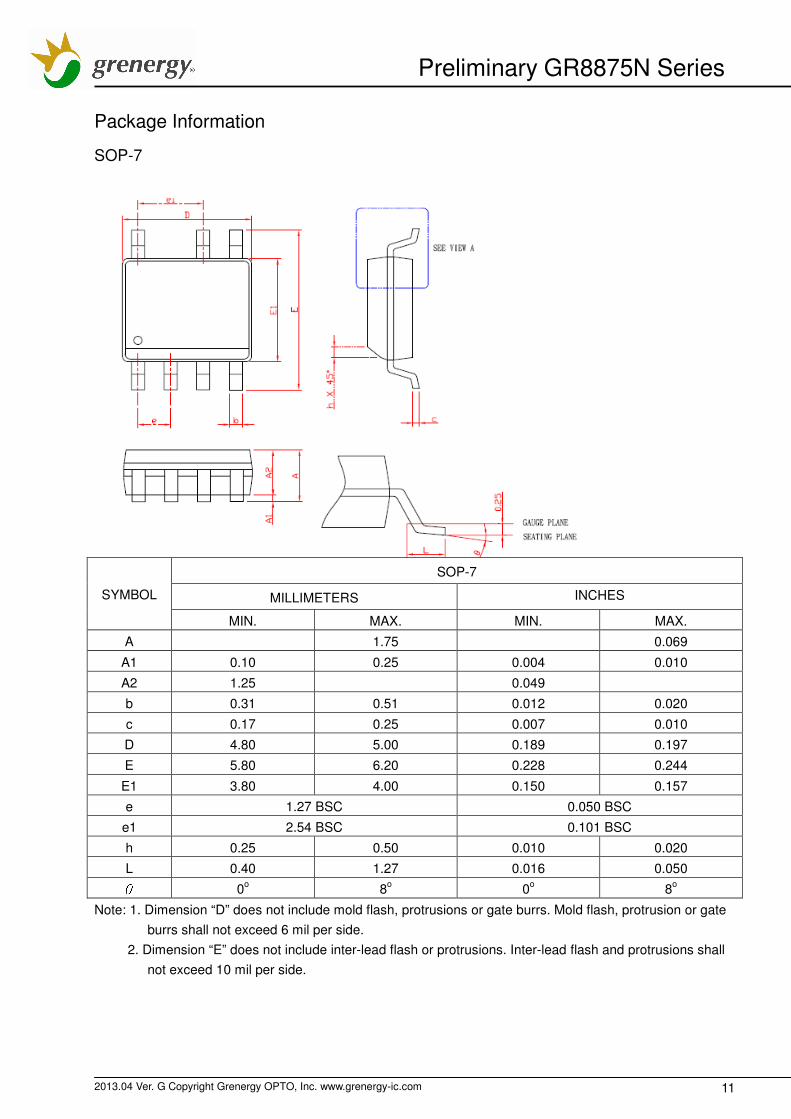
Package Information
SOP-8
SOP-8
MILLIMETERS INCHES SYMBOL
MIN. MAX. MIN. MAX.
A 1.75 0.069
A1 0.10 0.25 0.004 0.010
A2 1.25 0.049
b 0.31 0.51 0.012 0.020
c 0.17 0.25 0.007 0.010
D 4.80 5.00 0.189 0.197
E 5.80 6.20 0.228 0.244
E1 3.80 4.00 0.150 0.157
e 1.27 BSC 0.050 BSC
h 0.25 0.50 0.010 0.020
L 0.40 1.27 0.016 0.050 θ 0o 8
o 0
o 8
o
Note: 1. Followed from JEDEC MS-012 AA.
2. Dimension “D” does not include mold flash, protrusions or gate burrs. Mold flash, protrusion or gate
burrs shall not exceed 6 mil per side.
3. Dimension “E1” does not include inter-lead flash or protrusions. Inter-lead flash and protrusions shall
not exceed 10 mil per side.
2013.04 Ver. G Copyright Grenergy OPTO, Inc. www.grenergy-ic.com 11
Preliminary GR8875N Series
Package Information
SOP-7
SOP-7
MILLIMETERS INCHES SYMBOL
MIN. MAX. MIN. MAX.
A 1.75 0.069
A1 0.10 0.25 0.004 0.010
A2 1.25 0.049
b 0.31 0.51 0.012 0.020
c 0.17 0.25 0.007 0.010
D 4.80 5.00 0.189 0.197
E 5.80 6.20 0.228 0.244
E1 3.80 4.00 0.150 0.157
e 1.27 BSC 0.050 BSC
e1 2.54 BSC 0.101 BSC
h 0.25 0.50 0.010 0.020
L 0.40 1.27 0.016 0.050 θ 0o 8
o 0
o 8
o
Note: 1. Dimension “D” does not include mold flash, protrusions or gate burrs. Mold flash, protrusion or gate
burrs shall not exceed 6 mil per side.
2. Dimension “E” does not include inter-lead flash or protrusions. Inter-lead flash and protrusions shall
not exceed 10 mil per side.
2013.04 Ver. G Copyright Grenergy OPTO, Inc. www.grenergy-ic.com 12
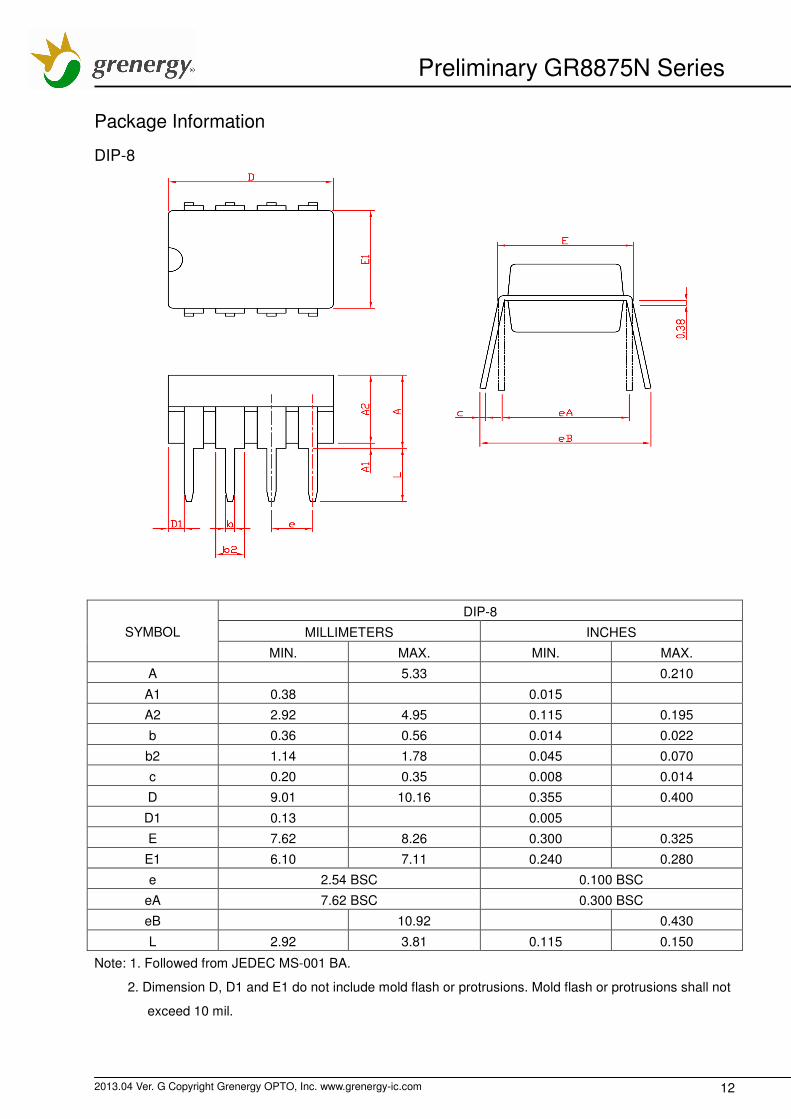
Preliminary GR8875N Series
Package Information
DIP-8
DIP-8
MILLIMETERS INCHES SYMBOL
MIN. MAX. MIN. MAX.
A 5.33 0.210
A1 0.38 0.015
A2 2.92 4.95 0.115 0.195
b 0.36 0.56 0.014 0.022
b2 1.14 1.78 0.045 0.070
c 0.20 0.35 0.008 0.014
D 9.01 10.16 0.355 0.400
D1 0.13 0.005
E 7.62 8.26 0.300 0.325
E1 6.10 7.11 0.240 0.280
e 2.54 BSC 0.100 BSC
eA 7.62 BSC 0.300 BSC
eB 10.92 0.430
L 2.92 3.81 0.115 0.150
Note: 1. Followed from JEDEC MS-001 BA.
2. Dimension D, D1 and E1 do not include mold flash or protrusions. Mold flash or protrusions shall not
exceed 10 mil.

2013.04 Ver. G Copyright Grenergy OPTO, Inc. www.grenergy-ic.com 13
Preliminary GR8875N Series
Carrier Tape & Reel Dimensions
SOP- 8/SOP-7
Application A H T1 C d D W E1 F
330.0±2.0 50 MIN. 12.4+2.00 -0.00
13.0+0.50 -0.20
1.5 MIN. 20.2 MIN. 12.0±0.30 1.75±0.10 5.5±0.05
P0 P1 P2 D0 D1 T A0 B0 K0 SOP-8/SOP7
4.0±0.10 8.0±0.10 2.0±0.05 1.5+0.10 -0.00 1.5 MIN.
0.6+0.00 -0.40 6.40±0.20 5.20±0.20 2.10±0.20
(mm)
Devices Per Unit
Application Carrier Width Cover Tape Width Devices Per Reel
SOP- 8/SOP-7 12 - 2500

2013.04 Ver. G Copyright Grenergy OPTO, Inc. www.grenergy-ic.com 14
Preliminary GR8875N Series
Taping Direction Information
SOP-8/ SOP-7
________________________________________________________________________ Grenergy OPTO, Inc. reserves the right to make corrections, modifications, enhancements, improvements, and other changes
to its products and services at any time and to discontinue any product or service without notice. Customers should obtain the
latest relevant information before placing orders and should verify that such information is current and complete.
Direction of feed Direction of feed


