
University of Alexandria
Faculty of Engineering
Department of Architecture
GREEN NANOARCHITECTURE
Thesis Submitted to the Department of Architecture
Faculty of Engineering – University of Alexandria
in partial fulfillment of the requirements of the degree of
Master of Science
in
Architecture
By Architect
Fahd Abd Elaziz Ahmed Omar Hemeida B.Sc. of Architecture
University of Alexandria
January 2010
GREEN NANOARCHITECTURE
Presented by
Fahd Abd Elaziz Ahmed Omar Hemeida B.Sc. of Architecture, University of Alexandria
For the degree of
Master of Science
in
Architecture
Examiners’ Committee: Approved
Prof.Dr. Mohamed Abdelall Ibrahim (Professor of architecture, department of architecture, Faculty
of Engineering, University of Alexandria) -----------------------------
Prof.Dr. Mohamed Tarek AlSayad (Professor of architecture, department of architecture, Faculty
of Engineering, University of Alexandria) -----------------------------
Prof.Dr. Mohamed Hisham Saudy (Professor of architecture, department of architecture, Faculty
Of Fine Arts, University of Alexandria) -----------------------------
Prof.Dr. Ibtehal Y. El-Bastawissi (Vice Dean of Graduate Studies and Research, Faculty of
Engineering, University of Alexandria) -----------------------------
Advisors’ Committee : Approved
Prof.Dr. Mohamed Abdelall Ibrahim (Professor of architecture, department of architecture, Faculty
of Engineering, University of Alexandria) -----------------------------
Prof.Dr. Osama Mahmoud Abd Elrahman (Professor of architecture, department of architecture, Faculty
of Engineering, University of Alexandria) -----------------------------

Acknowledgment
III
This research project would not have been possible without the support of many people. I wish to
submit this research to my supervisor , Prof. Dr. Mohamed Abdelall Ibrahim who , abundantly
helpful , offered invaluable assistance , support and guidance.
I would also like to convey thanks to the Ministry and the Faculty for providing the financial
means and library facilities.
I wish to express my love and gratitude to my beloved families and my cute fiancee for their
understanding & endless love through the duration of my studies.
Finally , very special Thanks to my dear Mom , to my beauty Fiancee and to my smart Sister for
always being there for me when I needed them.
Acknowledgment
Table of Contents
IV
Examiners' Committee.......................................................................................................... I
Advisors' Committee............................................................................................................. II
Acknowledgement................................................................................................................. III
Table of Contents.................................................................................................................. IV
List of Figures....................................................................................................................... VIII
List of Abbreviations............................................................................................................ XII
Abstract................................................................................................................................. XIV
Research Structure............................................................................................................... XV
Introduction.......................................................................................................................... XVI
Research Objectives ............................................................................................................ XVI
1.1. Introduction.................................................................................................................. 01
1.2. Definition of Nano........................................................................................................ 01
1.2.1. The beginning.................................................................................................... 02
1.2.2. A Word on Measurements................................................................................. 02
1.2.3. Nano for Science and Engineering.................................................................... 02
1.2.4. Nano scale.......................................................................................................... 03
1.3. Definition of Nanoscience............................................................................................ 03
1.4. Definition of Nanotechnology..................................................................................... 04
1.4.1. Introduction........................................................................................................ 04
1.4.2. History of Nanotechnology................................................................................ 05
1.4.3. Fundamental concepts........................................................................................ 06
1.4.3.A. Larger to smaller : a materials perspective........................................ 07
1.4.3.B. Simple to complex : a molecular prespective.................................... 08
1.4.3.C. Molecular nanotechnology : a long-term view.................................. 09
1.4.4. Current research................................................................................................. 10
1.4.4.A. Nano materials................................................................................... 10
1.4.4.A.i. Nano material science...................................................... 10
1.4.4.A.i.i Nanoscale in One Dimension....................... 11
1.4.4.A.i.ii. Nanoscale in Two Dimension....................... 12
1.4.4.A.i.iii.Nanoscale in Three Dimension.................... 12
1.4.4.A.ii. Nanotube Applications.................................................... 14
1.4.4.A.iii. Nanoparticle Applications............................................... 15
1.4.4.B. Bottom-up approaches....................................................................... 15
1.4.4.C. Top-down approaches....................................................................... 16
1.4.4.D. Functional approaches...................................................................... 16
1.4.4.E. Speculative......................................................................................... 17
1.4.5. Tools and techniques......................................................................................... 18
1.4.6. Nanotechnology Applications............................................................................ 19
1.4.6.A. Nanotechnology's potential to reduce greenhouse gases................... 19
1.4.6.B. Nanotechnology in Medicine............................................................. 21
CHAPTER ONE - NANOTECHNOLOGY
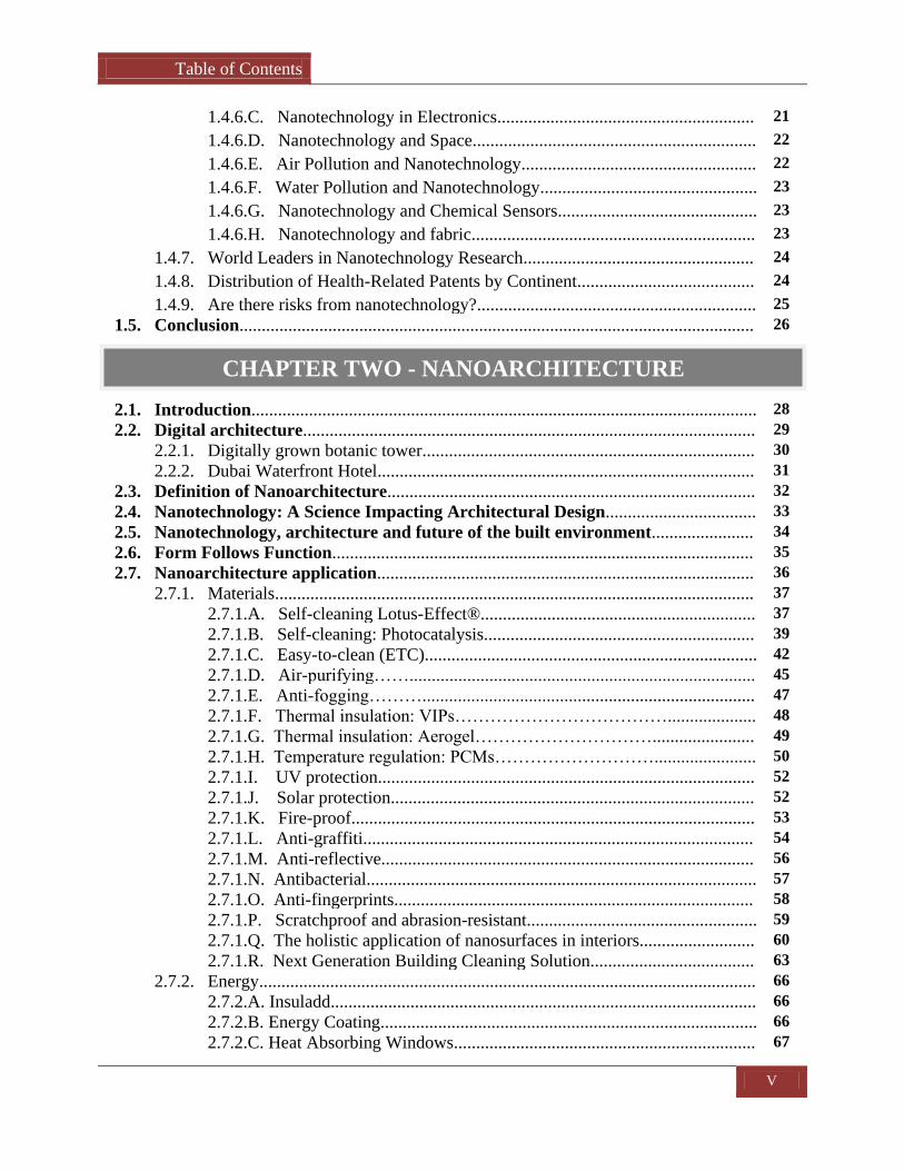
Table of Contents
V
1.4.6.C. Nanotechnology in Electronics.......................................................... 21
1.4.6.D. Nanotechnology and Space................................................................ 22
1.4.6.E. Air Pollution and Nanotechnology..................................................... 22
1.4.6.F. Water Pollution and Nanotechnology................................................. 23
1.4.6.G. Nanotechnology and Chemical Sensors............................................. 23
1.4.6.H. Nanotechnology and fabric................................................................ 23
1.4.7. World Leaders in Nanotechnology Research.................................................... 24
1.4.8. Distribution of Health-Related Patents by Continent........................................ 24
1.4.9. Are there risks from nanotechnology?............................................................... 25
1.5. Conclusion.................................................................................................................... 26
2.1. Introduction.................................................................................................................. 28
2.2. Digital architecture...................................................................................................... 29
2.2.1. Digitally grown botanic tower........................................................................... 30
2.2.2. Dubai Waterfront Hotel..................................................................................... 31
2.3. Definition of Nanoarchitecture................................................................................... 32
2.4. Nanotechnology: A Science Impacting Architectural Design.................................. 33
2.5. Nanotechnology, architecture and future of the built environment....................... 34
2.6. Form Follows Function............................................................................................... 35
2.7. Nanoarchitecture application..................................................................................... 36
2.7.1. Materials............................................................................................................ 37
2.7.1.A. Self-cleaning Lotus-Effect®.............................................................. 37
2.7.1.B. Self-cleaning: Photocatalysis............................................................. 39
2.7.1.C. Easy-to-clean (ETC)........................................................................... 42
2.7.1.D. Air-purifying…….............................................................................. 45
2.7.1.E. Anti-fogging………........................................................................... 47
2.7.1.F. Thermal insulation: VIPs……………………………….................... 48
2.7.1.G. Thermal insulation: Aerogel…………………………....................... 49
2.7.1.H. Temperature regulation: PCMs………………………....................... 50
2.7.1.I. UV protection..................................................................................... 52
2.7.1.J. Solar protection.................................................................................. 52
2.7.1.K. Fire-proof........................................................................................... 53
2.7.1.L. Anti-graffiti........................................................................................ 54
2.7.1.M. Anti-reflective.................................................................................... 56
2.7.1.N. Antibacterial........................................................................................ 57
2.7.1.O. Anti-fingerprints................................................................................. 58
2.7.1.P. Scratchproof and abrasion-resistant.................................................... 59
2.7.1.Q. The holistic application of nanosurfaces in interiors.......................... 60
2.7.1.R. Next Generation Building Cleaning Solution..................................... 63
2.7.2. Energy................................................................................................................ 66
2.7.2.A. Insuladd................................................................................................ 66
2.7.2.B. Energy Coating..................................................................................... 66
2.7.2.C. Heat Absorbing Windows.................................................................... 67
CHAPTER TWO - NANOARCHITECTURE
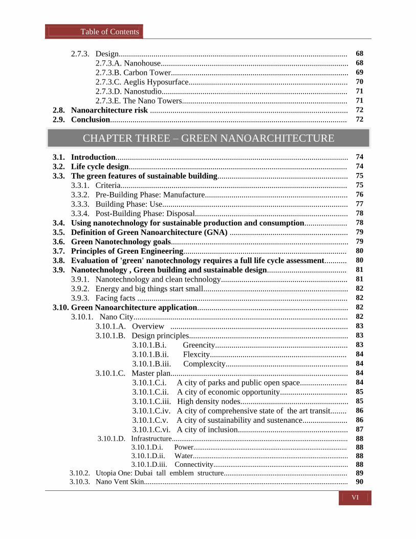
Table of Contents
VI
2.7.3. Design................................................................................................................ 68
2.7.3.A. Nanohouse............................................................................................ 68
2.7.3.B. Carbon Tower....................................................................................... 69
2.7.3.C. Aeglis Hyposurface.............................................................................. 70
2.7.3.D. Nanostudio........................................................................................... 71
2.7.3.E. The Nano Towers................................................................................. 71
2.8. Nanoarchitecture risk ................................................................................................. 72
2.9. Conclusion.................................................................................................................... 72
3.1. Introduction.................................................................................................................. 74
3.2. Life cycle design........................................................................................................... 74
3.3. The green features of sustainable building................................................................ 75
3.3.1. Criteria............................................................................................................... 75
3.3.2. Pre-Building Phase: Manufacture...................................................................... 76
3.3.3. Building Phase: Use........................................................................................... 77
3.3.4. Post-Building Phase: Disposal........................................................................... 78
3.4. Using nanotechnology for sustainable production and consumption..................... 78
3.5. Definition of Green Nanoarchitecture (GNA) .......................................................... 79
3.6. Green Nanotechnology goals....................................................................................... 79
3.7. Principles of Green Engineering................................................................................ 80
3.8. Evaluation of 'green' nanotechnology requires a full life cycle assessment........... 80
3.9. Nanotechnology , Green building and sustainable design....................................... 81
3.9.1. Nanotechnology and clean technology.............................................................. 81
3.9.2. Energy and big things start small....................................................................... 82
3.9.3. Facing facts ....................................................................................................... 82
3.10. Green Nanoarchitecture application.......................................................................... 82
3.10.1. Nano City......................................................................................................... 82
3.10.1.A. Overview ....................................................................................... 83
3.10.1.B. Design principles.............................................................................. 83
3.10.1.B.i. Greencity................................................................. 83
3.10.1.B.ii. Flexcity................................................................... 84
3.10.1.B.iii. Complexcity............................................................ 84
3.10.1.C. Master plan....................................................................................... 84
3.10.1.C.i. A city of parks and public open space....................... 84
3.10.1.C.ii. A city of economic opportunity................................. 85
3.10.1.C.iii. High density nodes..................................................... 85
3.10.1.C.iv. A city of comprehensive state of the art transit........ 86
3.10.1.C.v. A city of sustainability and sustenance...................... 86
3.10.1.C.vi. A city of inclusion...................................................... 87
3.10.1.D. Infrastructure.............................................................................................. 88
3.10.1.D.i. Power.................................................................................. 88
3.10.1.D.ii. Water................................................................................... 88
3.10.1.D.iii. Connectivity........................................................................ 88
3.10.2. Utopia One: Dubai tall emblem structure.................................................................. 89
3.10.3. Nano Vent Skin............................................................................................................. 90
CHAPTER THREE – GREEN NANOARCHITECTURE
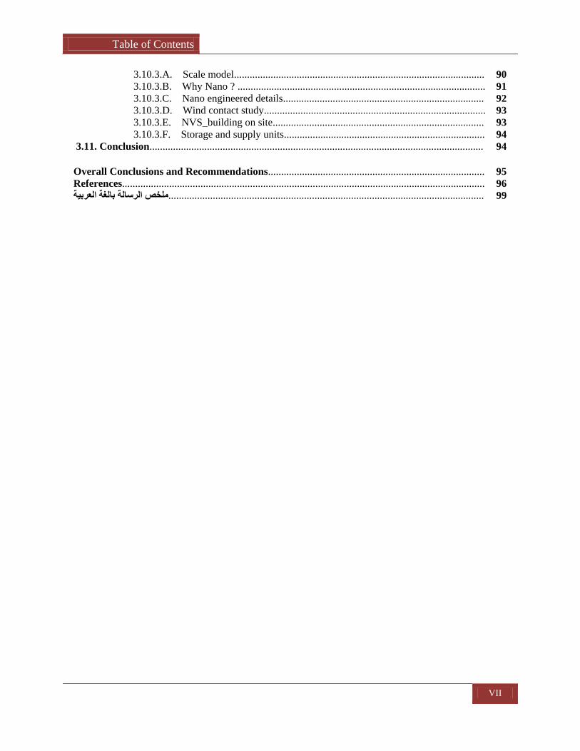
Table of Contents
VII
3.10.3.A. Scale model................................................................................................ 90
3.10.3.B. Why Nano ? ............................................................................................... 91
3.10.3.C. Nano engineered details............................................................................. 92
3.10.3.D. Wind contact study..................................................................................... 93
3.10.3.E. NVS_building on site................................................................................. 93
3.10.3.F. Storage and supply units............................................................................. 94
3.11. Conclusion................................................................................................................................ 94
Overall Conclusions and Recommendations................................................................................... 95
References........................................................................................................................................... 96
99 العربية بالغة الرسالة ملخص.........................................................................................................................
List of Figures
VIII
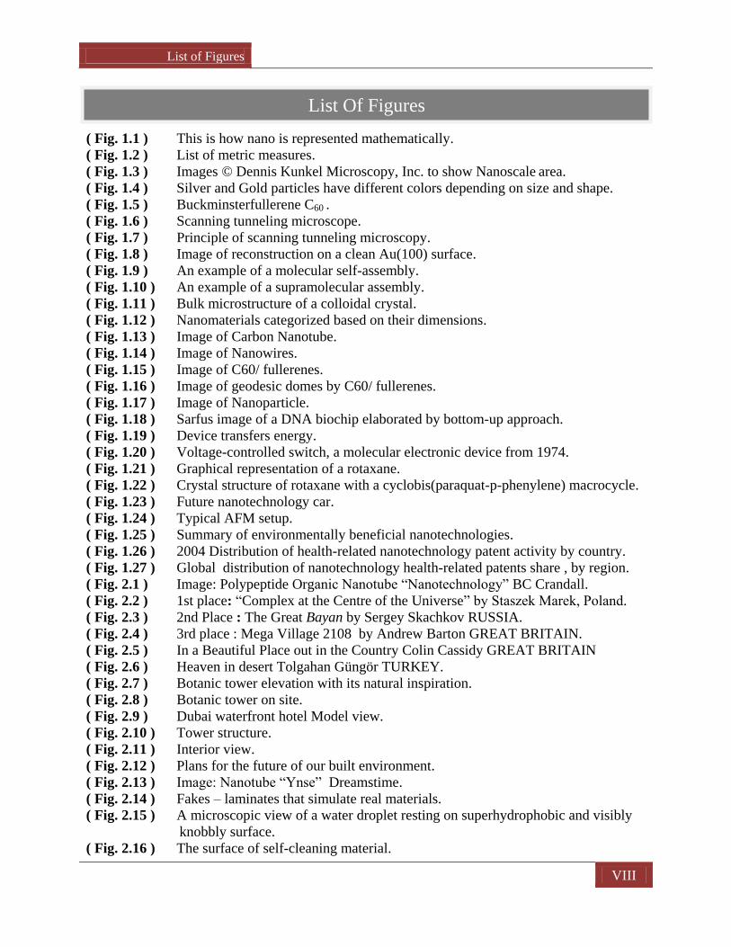
( Fig. 1.1 ) This is how nano is represented mathematically. ( Fig. 1.2 ) List of metric measures.
( Fig. 1.3 ) Images © Dennis Kunkel Microscopy, Inc. to show Nanoscale area.
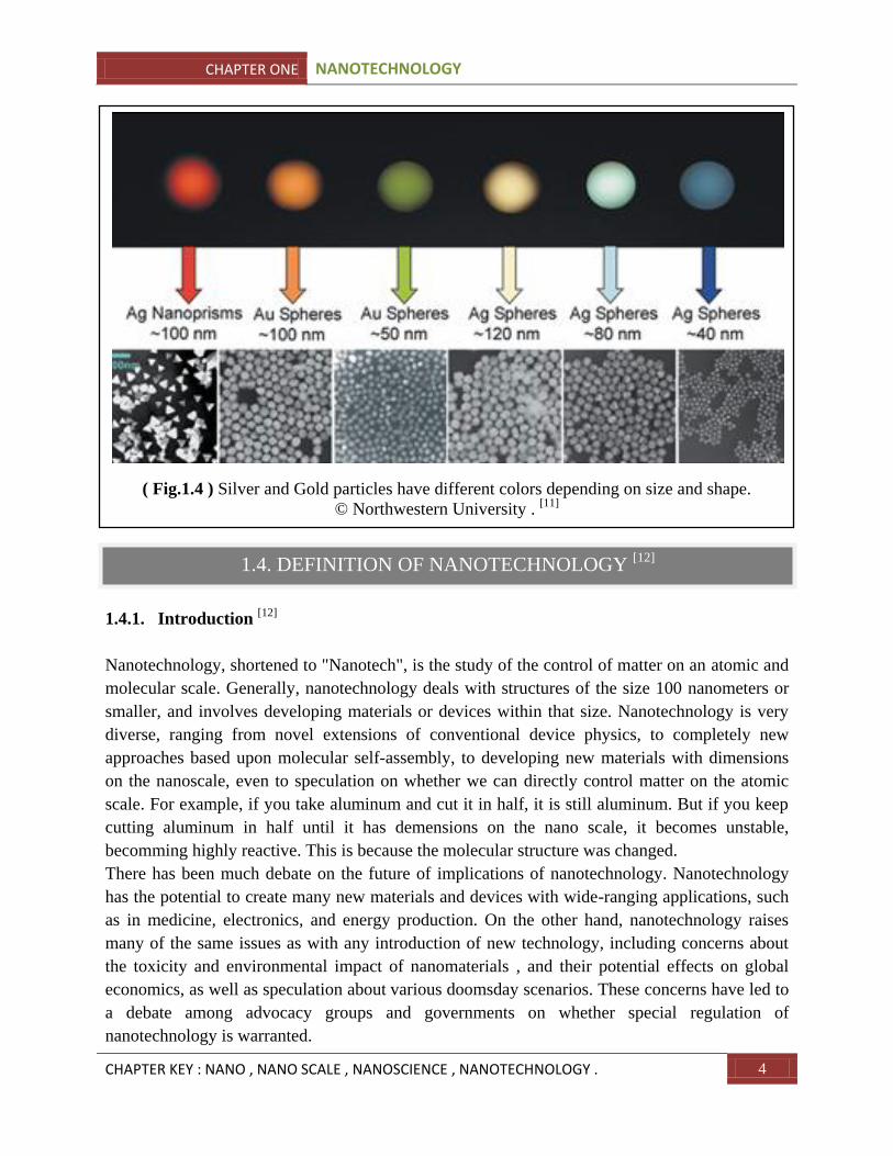
( Fig. 1.4 ) Silver and Gold particles have different colors depending on size and shape.
( Fig. 1.5 ) Buckminsterfullerene C60 .
( Fig. 1.6 ) Scanning tunneling microscope. ( Fig. 1.7 ) Principle of scanning tunneling microscopy. ( Fig. 1.8 ) Image of reconstruction on a clean Au(100) surface.
( Fig. 1.9 ) An example of a molecular self-assembly.
( Fig. 1.10 ) An example of a supramolecular assembly.
( Fig. 1.11 ) Bulk microstructure of a colloidal crystal.
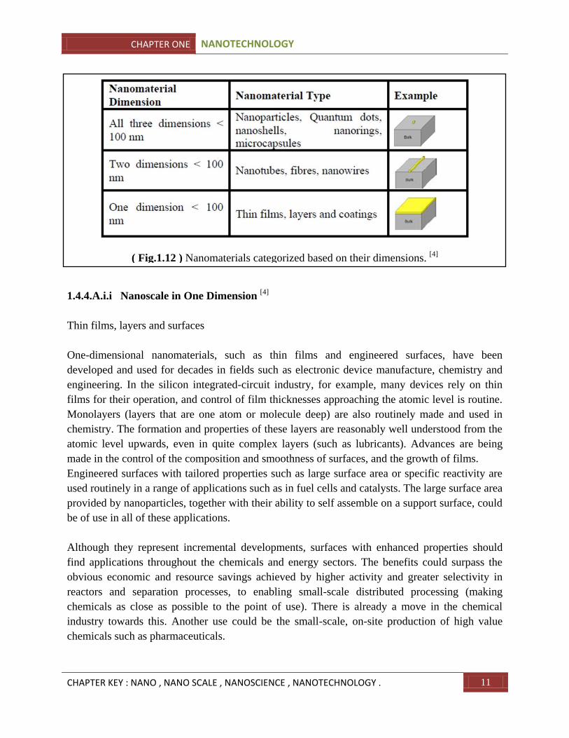
( Fig. 1.12 ) Nanomaterials categorized based on their dimensions.
( Fig. 1.13 ) Image of Carbon Nanotube.
( Fig. 1.14 ) Image of Nanowires.
( Fig. 1.15 ) Image of C60/ fullerenes.
( Fig. 1.16 ) Image of geodesic domes by C60/ fullerenes.
( Fig. 1.17 ) Image of Nanoparticle.
( Fig. 1.18 ) Sarfus image of a DNA biochip elaborated by bottom-up approach.
( Fig. 1.19 ) Device transfers energy.
( Fig. 1.20 ) Voltage-controlled switch, a molecular electronic device from 1974.
( Fig. 1.21 ) Graphical representation of a rotaxane.
( Fig. 1.22 ) Crystal structure of rotaxane with a cyclobis(paraquat-p-phenylene) macrocycle.
( Fig. 1.23 ) Future nanotechnology car.
( Fig. 1.24 ) Typical AFM setup.
( Fig. 1.25 ) Summary of environmentally beneficial nanotechnologies.
( Fig. 1.26 ) 2004 Distribution of health-related nanotechnology patent activity by country.
( Fig. 1.27 ) Global distribution of nanotechnology health-related patents share , by region.
( Fig. 2.1 ) Image: Polypeptide Organic Nanotube “Nanotechnology” BC Crandall.
( Fig. 2.2 ) 1st place: “Complex at the Centre of the Universe” by Staszek Marek, Poland.
( Fig. 2.3 ) 2nd Place : The Great Bayan by Sergey Skachkov RUSSIA.
( Fig. 2.4 ) 3rd place : Mega Village 2108 by Andrew Barton GREAT BRITAIN.
( Fig. 2.5 ) In a Beautiful Place out in the Country Colin Cassidy GREAT BRITAIN
( Fig. 2.6 ) Heaven in desert Tolgahan Güngör TURKEY.
( Fig. 2.7 ) Botanic tower elevation with its natural inspiration.
( Fig. 2.8 ) Botanic tower on site.
( Fig. 2.9 ) Dubai waterfront hotel Model view.
( Fig. 2.10 ) Tower structure.
( Fig. 2.11 ) Interior view.
( Fig. 2.12 ) Plans for the future of our built environment.
( Fig. 2.13 ) Image: Nanotube “Ynse” Dreamstime.
( Fig. 2.14 ) Fakes – laminates that simulate real materials.
( Fig. 2.15 ) A microscopic view of a water droplet resting on superhydrophobic and visibly
knobbly surface.
( Fig. 2.16 ) The surface of self-cleaning material.
List Of Figures
List of Figures
IX
( Fig. 2.17 ) Wood can be given an extremely water-repellent self-cleaning surface.
( Fig. 2.18 ) The diagram shows clearly the difference between conventional surfaces and the
Lotus-Effect.
( Fig. 2.19.A ) Ara Pacis Museum exterior.
( Fig. 2.19.B ) Ara Pacis interior exhibition halls.
( Fig. 2.19.C ) Ara Pacis Museum.
( Fig. 2.20 ) Before & After: On conventional tiles.
( Fig. 2.21 ) Oleophobic surfaces are resistant against oils and fats.
( Fig. 2.22 ) The diagram shows the basic process:Organic dirt & grime are broken down and
“decomposed”.
( Fig. 2.23 ) TiO2 and PVC coated white membranes in weathering tests.
( Fig. 2.24 ) These roof tiles, which have been on the market for some time, have self-
cleaning properties thanks to photocatalysis.
( Fig. 2.25 ) Narita International Airport.
( Fig. 2.26 ) MSV Arena Soccer Stadium.
( Fig. 2.27 ) “Roll-out marble” – impactresistant, fire-resistant, vapour permeable and yet
water-repellent & easy-to-clean.
( Fig. 2.28 ) A comparison of ceramic surfaces.
( Fig. 2.29 ) The angle of contact determines the hydrophobic degree of a surface.
( Fig. 2.30 ) Ultra-clean white surfaces of poolside armchairs achieved using water-repellent
surface coatings.
( Fig. 2.31 ) Waterclosets of the Science to Business Center Nanotronics & Bio.
( Fig. 2.32 ) Science to Business Center Nanotronics & Bio.
( Fig. 2.33 ) Kaldewei Kompetenz-center.
( Fig. 2.34 ) Exterior façade of Kaldewei Kompetenz-center.
( Fig. 2.35 ) Air-purifying materials such as plasterboard or acoustic panels.
( Fig. 2.36 ) The European Hq. of Hyundai Motors Europe in Offenbach, Germany,
is lined with air-purifying plasterboards.
( Fig. 2.37 ) Photocatalytic pavement surfacing.
( Fig. 2.38 ) Jubilee Church, Richard.
( Fig. 2.39 ) Air-purifying paving tiles.
( Fig. 2.40 ) Mirrors with anti-fogging coating do not steam up.
( Fig. 2.41 ) Different sized vacuum insulation panels in storage.
( Fig. 2.42 ) VIP insulation must be made to measure & fitted precisely on site.
( Fig. 2.43 ) Exterior of Seitzstrasse building.
( Fig. 2.44 ) Seitzstrasse building rooftop.
( Fig. 2.45 ) Aerogel in combination with glass.
( Fig. 2.46 ) Glass sample with black edging & aerogel-filled glazing cavity.
( Fig. 2.47 ) School extension.
( Fig. 2.48 ) Close-up of a phase-changing material embedded in glazing.
( Fig. 2.49 ) An opened microcapsule embedded in a concrete carrier matrix & of minute
paraffin-filled capsules in their solid state.
( Fig. 2.50 ) Layer composition of a decorative PCM gypsum plaster applied to a masonry
substrate.
( Fig. 2.51 ) "Sur Falveng" house for elderly people, façade.
List of Figures
X
( Fig. 2.52 ) Electron microscope image of UV-absorbent zinc oxide particles contained
within a clear varnish.
( Fig. 2.53 ) Electrochromatic glass with an ultra-thin nanocoating.
( Fig. 2.54 ) A robust sandwich panel.
( Fig. 2.55 ) The gel fill material in the glazing cavity.
( Fig. 2.56 ) Interior spaces in the Deutsch Post HQ.
( Fig. 2.57 ) Deutsche Post HQ. Germany.
( Fig. 2.58 ) The Brandenburg Gate in Berlin.
( Fig. 2.59 ) The UEFA headquarter in Nyon, Switzerland.
( Fig. 2.60 ) New Centre Ulm, Germany.
( Fig. 2.61 ) A Photovoltaic module.
( Fig. 2.62 ) Silica glass capsules.
( Fig. 2.63 ) An antibacterial material, such as that used for this light switch.
( Fig. 2.64 ) Nanoscalar silver particles contained in the glaze applied to ceramic.
( Fig. 2.65 ) Operation theatre interior shows the green antibacterial tiles.
( Fig. 2.66 ) The critical area around doorknobs.
( Fig. 2.67 ) The effect of the antifingerprint coating on this sheet of stainless steel is clearly
evident.
( Fig. 2.68 ) Abrasion tests indicate a surface's resilience against abrasion and wear and tear.
( Fig. 2.69 ) A schematic plan for a hotel room with a general strategic approach for the use
of nano functions.
( Fig. 2.70 ) A schematic plan for a patient room in a hospital with a general strategic
approach for the use of nano functions.
( Fig. 2.71 ) A schematic plan for an office room in a bank branch with a general strategic
approach for the use of nano functions.
( Fig. 2.72.A ) A granite wall which has become old and dirty after years of weathering.
( Fig. 2.72.B ) Before photocatalyst coating is applied on the surface.
( Fig. 2.72.C ) After 3 months of weathering.
( Fig. 2.73.A ) Before photocatalyst coating is applied on the surface .
( Fig. 2.73.B ) After 224 days of weathering.
( Fig. 2.74 ) Insuladd paints.
( Fig. 2.75 ) Energy coating.
( Fig. 2.76 ) Heat absorbing windows.
( Fig. 2.77.A ) Nanohouse 3D model.
( Fig. 2.77.B ) Nanohouse model.
( Fig. 2.78.A ) Section of Carbon Tower.
( Fig. 2.78.B ) The entrance of Carbon Tower.
( Fig. 2.78.C ) Carbon Tower model.
( Fig. 2.79 ) Aegis Hyposurface.
( Fig. 2.80 ) Nanostudio model.
( Fig. 2.81.A ) The Nano Towers.
( Fig. 2.81.B ) View between the towers.
( Fig. 2.81.C ) The canopy at ground level.
( Fig. 3.1) Three phases of the building material life cycle.
( Fig. 3.2 ) Key to the green features of sustainable building materials.
( Fig. 3.3 ) Typical life cycle of polymer nanocomposite.
List of Figures
XI
( Fig. 3.4 ) Nano City location.
( Fig. 3.5 ) Nano City Views.
( Fig. 3.6 ) Nano City a city of parks and public open space.
( Fig. 3.7 ) Nano City a city of economic opportunity.
( Fig. 3.8 ) Nano City high density nodes.
( Fig. 3.9 ) Nano City a city of comprehensive state of the art transit.
( Fig. 3.10 ) Nano City a city of sustainability and sustenance.
( Fig. 3.11 ) Nano City a city of sustainability and sustenance.
( Fig. 3.12 ) Power at Nano City.
( Fig. 3.13 ) Water resources at Nano City.
( Fig. 3.14 ) Nano City Wi Max and 3G connectivity.
( Fig. 3.15 ) 'utopia one' tower.
( Fig. 3.16 ) 'utopia one' power, through nano technology.
( Fig. 3.17 ) Nano Vent-Skin used on highway tunnels to power the lights.
( Fig. 3.18 ) Nano Vent-Skin used on road barriers to power the lights.
( Fig. 3.19 ) NVS wrapped around train tunnels.
( Fig. 3.20 ) Nano Vent-Skin used on existing buildings to supply electricity.
( Fig. 3.21 ) Each wind turbine is 25mm long by 10.8mm wide.
( Fig. 3.22 ) Images of the model against the sky, testing the final proportions.
( Fig. 3.23 ) NVS interacting with Sunlight, Wind and CO2.
( Fig. 3.24 ) Nano-structure components.
( Fig. 3.25 ) Zoom in showing the scale of nano engineered structures.
( Fig. 3.26 ) Nano Vent-Skin wind contact analysis.
( Fig. 3.27 ) Nano Vent-Skin wind contact study.
( Fig. 3.28 ) NVS View from the beach.
( Fig. 3.29 ) NVS Detail side view.
( Fig. 3.30 ) NVS Bay view.
( Fig. 3.31 ) NVS View from the interior.
( Fig. 3.32 ) Storage and supply units.
Abbreviations
XII
EPA
Environmental Protection Agency.
NM Nanometer (nm).
SI Systeme Internationale; International System.
NT Nanotechnology OR NANOTECH.
STM Scanning tunneling microscope.
DNA Deoxyribonucleic acid.
AU Gold.
PNAS-1981 Positional assembly to atomic specification.
ACS American Chemical Society.
UC BERKELEY University of California, Berkeley.
CO Carbon monoxide molecule. FE Iron atom. SEM Scanning electron microscope.
UCLA University of California, Los Angeles.
C60 Fullerenes.
EPIL Elan Pharma International .
NASA National Aeronautics and Space Administration.
UV ULTRAVIOLET.
ALD Atomic layer deposition.
NEMS Nanoelectromechanical systems.
MEMS Microelectromechanical systems.
AFM Atomic force microscope.
SAM Scanning acoustic microscope.
MBE Molecular beam epitaxy.
GHG Green House Gas.
Mte Millions of tonnes.
CO2 Carbon dioxide.
UK United Kingdom.
DTI Department of Trade and Industry.
U.S. United States.
S&T Science and technology.
CG Computer graphics.
NA Nanoarchitecture.
NYC NEW YORK CITY.
USA UNITED STATES OF AMERICA.
CVD Chemical vapor deposition.
TiO2 Titanium dioxide.
PVC Polyvinyl chloride.
PTFE Poly Tetra Fluoro Ethylene.
ETFE Ethylene tetrafluoroethylene.
MSV Meidericher Spielverein football team.
ETC Easy to Clean.
KKC Kaldewei Kompetenz-center.
List Of Abbreviations
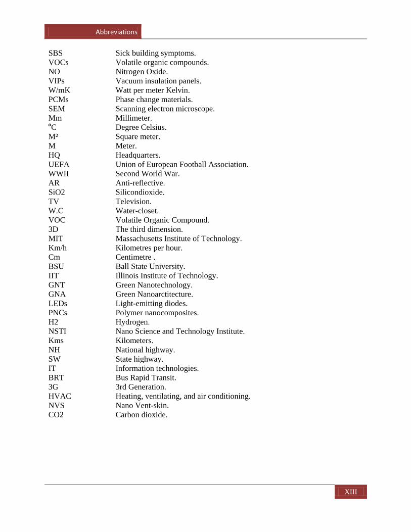
Abbreviations
XIII
SBS Sick building symptoms.
VOCs Volatile organic compounds.
NO Nitrogen Oxide.
VIPs Vacuum insulation panels.
W/mK Watt per meter Kelvin.
PCMs Phase change materials.
SEM Scanning electron microscope.
Mm Millimeter. oC Degree Celsius.
M² Square meter.
M Meter.
HQ Headquarters.
UEFA Union of European Football Association.
WWII Second World War.
AR Anti-reflective.
SiO2 Silicondioxide.
TV Television.
W.C Water-closet.
VOC Volatile Organic Compound.
3D The third dimension.
MIT Massachusetts Institute of Technology.
Km/h Kilometres per hour.
Cm Centimetre .
BSU Ball State University.
IIT Illinois Institute of Technology.
GNT Green Nanotechnology.
GNA Green Nanoarctitecture.
LEDs Light-emitting diodes.
PNCs Polymer nanocomposites.
H2 Hydrogen.
NSTI Nano Science and Technology Institute.
Kms Kilometers.
NH National highway.
SW State highway.
IT Information technologies.
BRT Bus Rapid Transit.
3G 3rd Generation.
HVAC Heating, ventilating, and air conditioning.
NVS Nano Vent-skin.
CO2 Carbon dioxide.
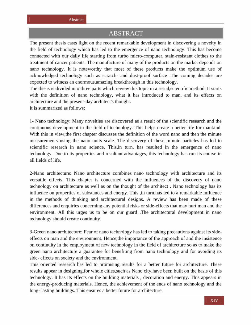
Abstract
XIV
The present thesis casts light on the recent remarkable development in discovering a novelty in
the field of technology which has led to the emergence of nano technology. This has become
connected with our daily life starting from turbo micro-computer, stain-resistant clothes to the
treatment of cancer patients. The manufacture of many of the products on the market depends on
nano technology. It is noteworthy that most of these products make the optimum use of
acknowledged technology such as scratch- and dust-proof surface .The coming decades are
expected to witness an enormous,amazing breakthrough in this technology.
The thesis is divided into three parts which review this topic in a serial,scientific method. It starts
with the definition of nano technology, what it has introduced to man, and its effects on
architecture and the present-day architect's thought.
It is summarized as follows:
1- Nano technology: Many novelties are discovered as a result of the scientific research and the
continuous development in the field of technology. This helps create a better life for mankind.
With this in view,the first chapter discusses the definition of the word nano and then the minute
measurements using the nano units scale. The discovery of these minute particles has led to
scientific research in nano science. This,in turn, has resulted in the emergence of nano
technology. Due to its properties and resultant advantages, this technology has run its course in
all fields of life.
2-Nano architecture: Nano architecture combines nano technology with architecture and its
versatile effects. This chapter is concerned with the influences of the discovery of nano
technology on architecture as well as on the thought of the architect . Nano technology has its
influence on properties of substances and energy. This ,in turn,has led to a remarkable influence
in the methods of thinking and architectural designs. A review has been made of these
differences and enquiries concerning any potential risks or side-effects that may hurt man and the
environment. All this urges us to be on our guard .The architectural development in nano
technology should create continuity.
3-Green nano architecture: Fear of nano technology has led to taking precautions against its side-
effects on man and the environment. Hence,the importance of the approach of and the insistence
on continuity in the employment of new technology in the field of architecture so as to make the
green nano architecture a guarantee for benefiting from nano technology and for avoiding its
side- effects on society and the environment.
This oriented research has led to promising results for a better future for architecture. These
results appear in designing,for whole cities,such as Nano city,have been built on the basis of this
technology. It has its effects on the building materials , decoration and energy. This appears in
the energy-producing materials. Hence, the achievement of the ends of nano technology and the
long- lasting buildings. This ensures a better future for architecture.
ABSTRACT
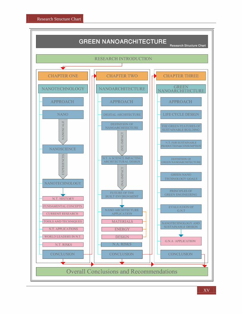
Research Structure Chart
XV
Introduction
XVI
Nanotechnology, the science of manufacturing material at a tiny scale, creates new possibilities
to make dramatic improvements to our lives.Yet, the uncertain impacts to health, the
environment, and society that may arise with this emerging technology demand our urgent
attention. If we want to ensure that the benefits of nanotechnology far exceed any risks, we need
an oversight system that assures safety while providing transparency for both businesses and the
public. Over the past two years, nanotechnology has moved dramatically from the lab into the
marketplace.
Today, there are more than 450 manufacturer-identified nanotechnology-enabled products in the
commercial market and “over 600 raw materials, intermediate components and industrial
equipment items” used by nano manufacturers (U.S. EPA 2007) and many more are sure to
follow, given the large investments in research, development, and commercialization. These
products open a wide array of questions concerning the risk of nanomaterials to workers,
consumers, and the environment and provide new challenges to regulatory agencies. If we expect
to see an effective regulatory system for nanotechnology, the Environmental Protection Agency
(EPA) and other players must come together today and take the necessary steps to evaluate
different approaches and move forward with a plan of action.
A "strong marriage" between nanotechnology and the principles and practices of green chemistry
and green engineering "holds the key to building an environmentally sustainable society in the
21st century," concludes Green Nanotechnology: It's Easier Than You Think.
The report explores potentially beneficial links between nanotechnology – essentially, science
and engineering practiced on the molecular scale – and green chemistry and engineering, which
aim to minimize environmental impacts through resource-conserving and waste-eliminating
improvements in processes and products. It concludes with recommendations for proactive
federal policy measures to help the fast developing field of nanotechnology to "grow up" green.
1. Identified nanotechnology as the separation line between the present and the future, that
reveals the secrets of the impact on the Domains of life .
2. Clarify the importance of nanotechnology to the field of Architecture and the integration
between them to show the nanoarchitecture and focus on the influence in architecture and the
architect thinking in the design of buildings .
3. Meditation for the better by using nanotechnology to achieve sustainability in architecture
INTRODUCTION [40] [7]
RESEARCH OBJECTIVES [44]
CHAPTER ONE
NANOTECHNOLOGY
N A N O T E C H N O L O G Y
CHAPTER ONE NANOTECHNOLOGY
CHAPTER KEY : NANO , NANO SCALE , NANOSCIENCE , NANOTECHNOLOGY . 1
If one were to ask at random people to identify the most pressing present and future global
challenges with potential technological fixes, the list might include cheap and clean energy,
increased demand for potable water, reduced environmental pollution, world hunger, national
security, and cures for diseases such as cancer. Ask those same people what nanotechnology is
and you‟re likely to get one of two responses by far the most common : “I think it has something
to do with tiny little machines that swim through your body and fix things?” (Foresight and
Governance Project 2003) This is likely to change in the next couple of years, because only one
field of technical research promises to develop solutions for all the aforementioned challenges.
That field is nanotechnology.
Nanotechnology is an exciting area of scientific development which promises „more for less‟. It
offers ways to create smaller, cheaper, lighter and faster devices that can do more and cleverer
things, use less raw materials and consume less energy.
It represents a whole new method of manufacturing, which achieves control at the atomic scale.
It is better described as a collection of technologies which are genuinely “disruptive” – that is,
they will render many existing technologies and processes obsolete and create entirely new types
of products.
Over the coming years and decades, nanotechnologies are set to make an enormous impact on
manufacturing and service industries, on electronics, information technology, and on many other
areas of life, from medicine to energy conservation.
Just how large this impact will be is not easily quantifiable, but some forecasts have placed the
worldwide market for nanotechnology–related products at around £105 billion by 2005 and £700
billion by 2010 . Nanotechnology has been described as a new industrial revolution.
Over the past decade a new term has entered the English vocabulary and that word is
“nano” We hear the word in movies. It is mentioned on television and in newspapers
and magazines. Futurists say it will pave the way for unimaginable new possibilities.
There are many different opinions about where this new field will take us, but everyone
agrees that this science and the new technologies that come from it have the possibility
of significantly impacting our world.
1.2. DEFINITION OF NANO [24]
1.1. INTRODUCTION [8] [3]
CHAPTER ONE NANOTECHNOLOGY
CHAPTER KEY : NANO , NANO SCALE , NANOSCIENCE , NANOTECHNOLOGY . 2
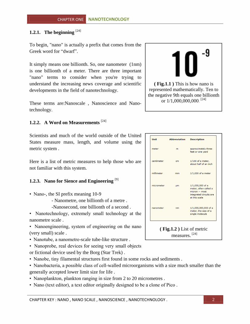
1.2.1. The beginning [24]
To begin, "nano" is actually a prefix that comes from the
Greek word for “dwarf”.
It simply means one billionth. So, one nanometer (1nm)
is one billionth of a meter. There are three important
"nano" terms to consider when you're trying to
understand the increasing news coverage and scientific
developments in the field of nanotechnology.
These terms are:Nanoscale , Nanoscience and Nano-
technology.
1.2.2. A Word on Measurements [24]
Scientists and much of the world outside of the United
States measure mass, length, and volume using the
metric system .
Here is a list of metric measures to help those who are
not familiar with this system.
1.2.3. Nano for Sience and Engineering [9]
• Nano-, the SI prefix meaning 10-9
- Nanometre, one billionth of a metre .
-Nanosecond, one billionth of a second .
• Nanotechnology, extremely small technology at the
nanometre scale .
• Nanoengineering, system of engineering on the nano
(very small) scale .
• Nanotube, a nanometre-scale tube-like structure .
• Nanoprobe, real devices for seeing very small objects
or fictional device used by the Borg (Star Trek) .
• Nanobe, tiny filamental structures first found in some rocks and sediments .
• Nanobacteria, a possible class of cell-walled microorganisms with a size much smaller than the
generally accepted lower limit size for life .
• Nanoplankton, plankton ranging in size from 2 to 20 micrometres .
• Nano (text editor), a text editor originally designed to be a clone of Pico .
( Fig.1.1 ) This is how nano is
represented mathematically. Ten to
the negative 9th equals one billionth
or 1/1,000,000,000. [24]
( Fig.1.2 ) List of metric
measures. [24]
CHAPTER ONE NANOTECHNOLOGY
CHAPTER KEY : NANO , NANO SCALE , NANOSCIENCE , NANOTECHNOLOGY . 3
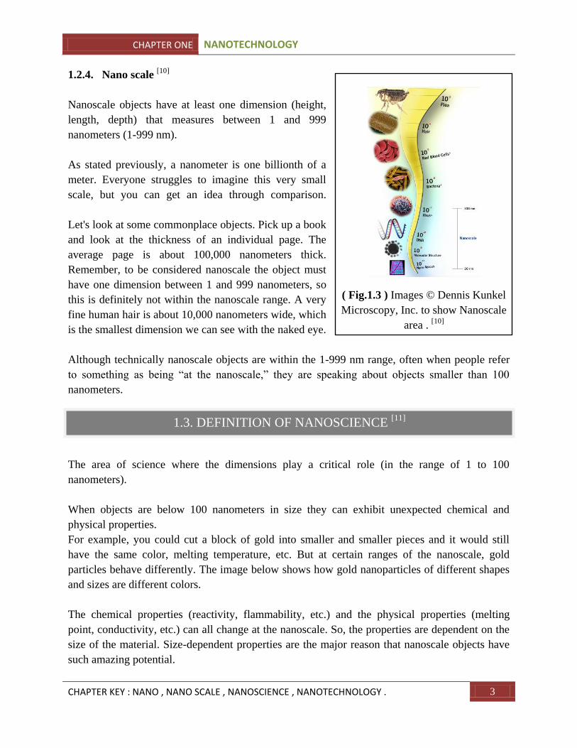
1.2.4. Nano scale [10]
Nanoscale objects have at least one dimension (height,
length, depth) that measures between 1 and 999
nanometers (1-999 nm).
As stated previously, a nanometer is one billionth of a
meter. Everyone struggles to imagine this very small
scale, but you can get an idea through comparison.
Let's look at some commonplace objects. Pick up a book
and look at the thickness of an individual page. The
average page is about 100,000 nanometers thick.
Remember, to be considered nanoscale the object must
have one dimension between 1 and 999 nanometers, so
this is definitely not within the nanoscale range. A very
fine human hair is about 10,000 nanometers wide, which
is the smallest dimension we can see with the naked eye.
Although technically nanoscale objects are within the 1-999 nm range, often when people refer
to something as being “at the nanoscale,” they are speaking about objects smaller than 100
nanometers.
The area of science where the dimensions play a critical role (in the range of 1 to 100
nanometers).
When objects are below 100 nanometers in size they can exhibit unexpected chemical and
physical properties.
For example, you could cut a block of gold into smaller and smaller pieces and it would still
have the same color, melting temperature, etc. But at certain ranges of the nanoscale, gold
particles behave differently. The image below shows how gold nanoparticles of different shapes
and sizes are different colors.
The chemical properties (reactivity, flammability, etc.) and the physical properties (melting
point, conductivity, etc.) can all change at the nanoscale. So, the properties are dependent on the
size of the material. Size-dependent properties are the major reason that nanoscale objects have
such amazing potential.
( Fig.1.3 ) Images © Dennis Kunkel
Microscopy, Inc. to show Nanoscale
area . [10]
1.3. DEFINITION OF NANOSCIENCE [11]
CHAPTER ONE NANOTECHNOLOGY
CHAPTER KEY : NANO , NANO SCALE , NANOSCIENCE , NANOTECHNOLOGY . 4
1.4.1. Introduction [12]
Nanotechnology, shortened to "Nanotech", is the study of the control of matter on an atomic and
molecular scale. Generally, nanotechnology deals with structures of the size 100 nanometers or
smaller, and involves developing materials or devices within that size. Nanotechnology is very
diverse, ranging from novel extensions of conventional device physics, to completely new
approaches based upon molecular self-assembly, to developing new materials with dimensions
on the nanoscale, even to speculation on whether we can directly control matter on the atomic
scale. For example, if you take aluminum and cut it in half, it is still aluminum. But if you keep
cutting aluminum in half until it has demensions on the nano scale, it becomes unstable,
becomming highly reactive. This is because the molecular structure was changed.
There has been much debate on the future of implications of nanotechnology. Nanotechnology
has the potential to create many new materials and devices with wide-ranging applications, such
as in medicine, electronics, and energy production. On the other hand, nanotechnology raises
many of the same issues as with any introduction of new technology, including concerns about
the toxicity and environmental impact of nanomaterials , and their potential effects on global
economics, as well as speculation about various doomsday scenarios. These concerns have led to
a debate among advocacy groups and governments on whether special regulation of
nanotechnology is warranted.
( Fig.1.4 ) Silver and Gold particles have different colors depending on size and shape.
© Northwestern University . [11]
1.4. DEFINITION OF NANOTECHNOLOGY [12]
CHAPTER ONE NANOTECHNOLOGY
CHAPTER KEY : NANO , NANO SCALE , NANOSCIENCE , NANOTECHNOLOGY . 5
1.4.2. History of Nanotechnology [12]
The first use of the concepts in 'nano-technology' (but
pre-dating use of that name) was in "There's Plenty of
Room at the Bottom," a talk given by physicist Richard
Feynman at an American Physical Society meeting at
Caltech on December 29, 1959. Feynman described a
process by which the ability to manipulate individual
atoms and molecules might be developed, using one set
of precise tools to build and operate another
proportionally smaller set, so on down to the needed
scale. In the course of this, he noted, scaling issues
would arise from the changing magnitude of various
physical phenomena: gravity would become less
important, surface tension and Van der Waals attraction
would become more important, etc. This basic idea
appears plausible, and exponential assembly enhances it
with parallelism to produce a useful quantity of end
products.
The term "nanotechnology" was defined by Tokyo
Science University Professor Norio Taniguchi in a 1974
paper as follows: "'Nano-technology' mainly consists of
the processing , the separation , the consolidation, and
the deformation of materials by one atom or by one
molecule.
" In the 1980s the basic idea of this definition was
explored in much more depth by Dr. K. Eric Drexler,
who promoted the technological significance of nano-
scale phenomena and devices through speeches and the
books Engines of Creation: The Coming Era of
Nanotechnology (1986) and Nanosystems: Molecular
Machinery, Manufacturing, and Computation, and so the
term acquired its current sense. Engines of Creation: The
Coming Era of Nanotechnology is considered the first
book on the topic of nanotechnology. Nanotechnology
and nanoscience got started in the early 1980s with two
major developments: the birth of cluster science and the
invention of the scanning tunneling microscope (STM).
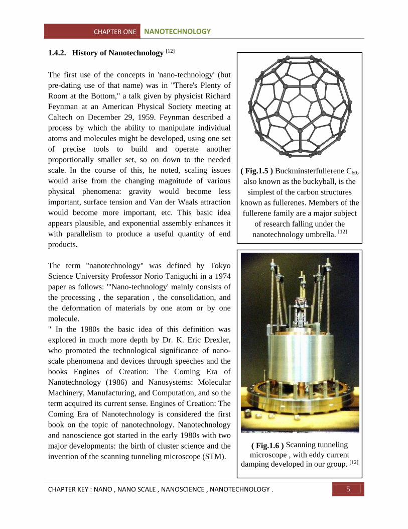
( Fig.1.5 ) Buckminsterfullerene C60,
also known as the buckyball, is the
simplest of the carbon structures
known as fullerenes. Members of the
fullerene family are a major subject
of research falling under the
nanotechnology umbrella. [12]
( Fig.1.6 ) Scanning tunneling
microscope , with eddy current
damping developed in our group. [12]
CHAPTER ONE NANOTECHNOLOGY
CHAPTER KEY : NANO , NANO SCALE , NANOSCIENCE , NANOTECHNOLOGY . 6
This development led to the discovery of fullerenes in 1985 and carbon nanotubes a few years
later. In another development, the synthesis and properties of semiconductor nanocrystals was
studied; this led to a fast increasing number of metal oxide nanoparticles of quantum dots. The
atomic force microscope was invented six years after the STM was invented. In 2000, the United
States National Nanotechnology Initiative was founded to coordinate Federal nanotechnology
research and development.
1.4.3. Fundamental concepts [12]
One nanometer (nm) is one billionth, or 10−9, of a meter. By comparison, typical carbon-carbon
bond lengths, or the spacing between these atoms in a molecule, are in the range 0.12–0.15 nm,
and a DNA double-helix has a diameter around 2 nm. On the other hand, the smallest cellular
life-forms, the bacteria of the genus Mycoplasma, are around 200 nm in length.
To put that scale in another context, the comparative size of a nanometer to a meter is the same
as that of a marble to the size of the earth. Or another way of putting it: a nanometer is the
amount a man's beard grows in the time it takes him to raise the razor to his face.
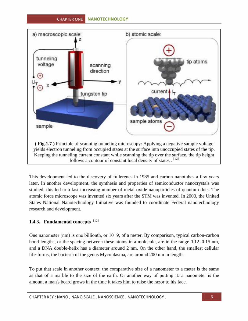
( Fig.1.7 ) Principle of scanning tunneling microscopy: Applying a negative sample voltage
yields electron tunneling from occupied states at the surface into unoccupied states of the tip.
Keeping the tunneling current constant while scanning the tip over the surface, the tip height
follows a contour of constant local density of states . [12]
CHAPTER ONE NANOTECHNOLOGY
CHAPTER KEY : NANO , NANO SCALE , NANOSCIENCE , NANOTECHNOLOGY . 7
Two main approaches are used in nanotechnology. In the "bottom-up" approach, materials and
devices are built from molecular components which assemble themselves chemically by
principles of molecular recognition. In the "top-down" approach, nano-objects are constructed
from larger entities without atomic-level control.
Areas of physics such as nanoelectronics, nanomechanics and nanophotonics have been evolved
during the last decades to provide a basic scientific foundation of nanotechnology.
1.4.3.A. Larger to smaller : a materials perspective [12]
A number of physical phomomena become pronounced
as the size of the system decreases. These include
statistical mechanical effects, as well as quantum
mechanical effects, for example the “quantum size
effect” where the electronic properties of solids are
altered with great reductions in particle size. This effect
does not come into play by going from macro to micro
dimensions. However, it becomes dominant when the
nanometer size range is reached.Additionally, a number
of physical (mechanical, electrical, optical, etc.)
properties change when compared to macroscopic
systems. One example is the increase in surface area to
volume ratio altering mechanical, thermal and catalytic
properties of materials.Diffusion and reactions at
nanoscale, nanostructures materials and nanodevices
with fast ion transport are generally referred to
nanoionics. Novel mechanical properties of nanosystems
are of interest in the nanomechanics research. The
catalytic activity of nanomaterials also opens potential
risks in their interaction with biomaterials.
Materials reduced to the nanoscale can show different properties compared to what they exhibit
on a macroscale, enabling unique applications. For instance, opaque substances become
transparent (copper); stable materials turn combustible (aluminum); solids turn into liquids at
room temperature (gold); insulators become conductors (silicon).
A material such as gold, which is chemically inert at normal scales, can serve as a potent
chemical catalyst at nanoscales. Much of the fascination with nanotechnology stems from these
quantum and surface phenomena that matter exhibits at the nanoscale.
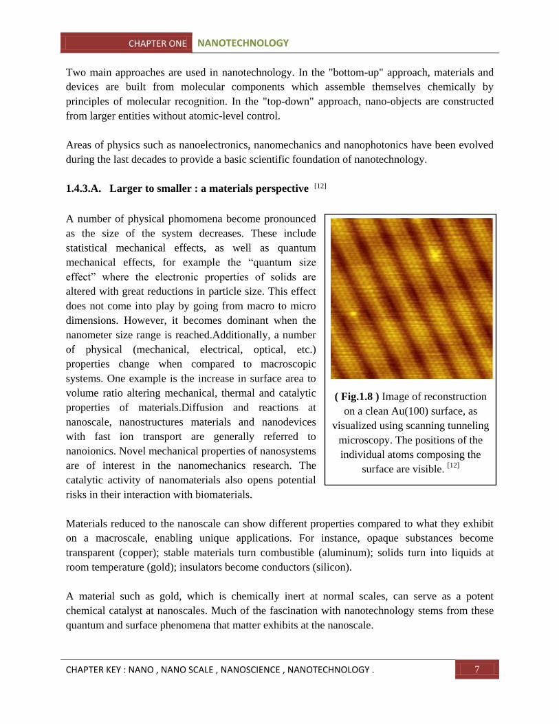
( Fig.1.8 ) Image of reconstruction
on a clean Au(100) surface, as
visualized using scanning tunneling
microscopy. The positions of the
individual atoms composing the
surface are visible. [12]

CHAPTER ONE NANOTECHNOLOGY
CHAPTER KEY : NANO , NANO SCALE , NANOSCIENCE , NANOTECHNOLOGY . 8
1.4.3.B. Simple to complex : a molecular perspective [12]
Modern synthetic chemistry has reached the point where
it is possible to prepare small molecules to almost any
structure. These methods are used today to produce a
wide variety of useful chemicals such as pharma-
ceuticals or commercial polymers. This ability raises the
question of extending this kind of control to the next-
larger level, seeking methods to assemble these single
molecules into supramolecular assemblies consisting of
many molecules arranged in a well defined manner.
These approaches utilize the concepts of molecular
self-assembly and/or supramolecular chemistry to
automatically arrange themselves into some useful
conformation through a bottom-up approach.
The concept of molecular recognition is especially
important: molecules can be designed so that a specific
conformation or arrangement is favored due to non-
covalent intermolecular forces. The Watson-Crick
basepairing rules are a direct result of this, as is the
specificity of an enzyme being targeted to a single
substrate, or the specific folding of the protein itself.
Thus, two or more components can be designed to be
complementary and mutually attractive so that they
make a more complex and useful whole.
Such bottom-up approaches should be able to produce
devices in parallel and much cheaper than top-down
methods, but could potentially be overwhelmed as the
size and complexity of the desired assembly increases.
Most useful structures require complex and
thermodynamically unlikely arrangements of atoms.
Nevertheless, there are many examples of self-assembly
based on molecular recognition in biology, most notably
Watson-Crick basepairing and enzyme-substrate
interactions. The challenge for nanotechnology is
whether these principles can be used to engineer novel
constructs in addition to natural ones.
( Fig.1.9 ) An example of a
molecular self-assembly through
hydrogen bonds reported by Meijer
and coworkers. [12]
( Fig.1.10 ) An example of a
supramolecular assembly reported
by Atwood and coworkers in
Science 2005, 309, 2037. [12]
CHAPTER ONE NANOTECHNOLOGY
CHAPTER KEY : NANO , NANO SCALE , NANOSCIENCE , NANOTECHNOLOGY . 9
1.4.3.C. Molecular nanotechnology : a long-term view [12]
Molecular nanotechnology, sometimes called molecular manufacturing, is a term given to the
concept of engineered nanosystems (nanoscale machines) operating on the molecular scale. It is
especially associated with the concept of a molecular assembler, a machine that can produce a
desired structure or device atom-by-atom using the principles of mechanosynthesis.
Manufacturing in the context of productive nanosystems is not related to, and should be clearly
distinguished from, the conventional technologies used to manufacture nanomaterials such as
carbon nanotubes and nanoparticles.
When the term "nanotechnology" was independently coined and popularized by Eric Drexler
(who at the time was unaware of an earlier usage by Norio Taniguchi), it referred to a future
manufacturing technology based on molecular machine systems. The premise was that molecular
scale biological analogies of traditional machine components demonstrated molecular machines
were possible: by the countless examples found in biology, it is known that sophisticated,
stochastically optimised biological machines can be produced.
It is hoped that developments in nanotechnology will make possible their construction by some
other means, perhaps using biomimetic principles. However, Drexler and other researchers have
proposed that advanced nanotechnology, although perhaps initially implemented by biomimetic
means, ultimately could be based on mechanical engineering principles, namely, a manufacturing
technology based on the mechanical functionality of these components (such as gears, bearings,
motors, and structural members) that would enable programmable, positional assembly to atomic
specification (PNAS-1981). The physics and engineering performance of exemplar designs were
analyzed in Drexler's book Nanosystems.
In general it is very difficult to assemble devices on the atomic scale, as all one has to position
atoms are other atoms of comparable size and stickiness. Another view, put forth by Carlo
Montemagno , is that future nanosystems will be hybrids of silicon technology and biological
molecular machines. Yet another view, put forward by the late Richard Smalley, is that
mechanosynthesis is impossible due to the difficulties in mechanically manipulating individual
molecules.
This led to an exchange of letters in the ACS publication Chemical & Engineering News in
2003. Though biology clearly demonstrates that molecular machine systems are possible, non-
biological molecular machines are today only in their infancy. Leaders in research on non-
biological molecular machines are Dr. Alex Zettl and his colleagues at Lawrence Berkeley
Laboratories and UC Berkeley. They have constructed at least three distinct molecular devices
whose motion is controlled from the desktop with changing voltage: a nanotube nanomotor, a
molecular actuator, and a nanoelectromechanical relaxation oscillator.
CHAPTER ONE NANOTECHNOLOGY
CHAPTER KEY : NANO , NANO SCALE , NANOSCIENCE , NANOTECHNOLOGY . 10
An experiment indicating that positional molecular assembly is possible was performed by Ho
and Lee at Cornell University in 1999. They used a scanning tunneling microscope to move an
individual carbon monoxide molecule (CO) to an individual iron atom (Fe) sitting on a flat silver
crystal, and chemically bound the CO to the Fe by applying a voltage.
1.4.4. Current research [12]
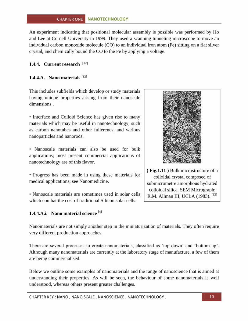
1.4.4.A. Nano materials [12]
This includes subfields which develop or study materials
having unique properties arising from their nanoscale
dimensions .
• Interface and Colloid Science has given rise to many
materials which may be useful in nanotechnology, such
as carbon nanotubes and other fullerenes, and various
nanoparticles and nanorods.
• Nanoscale materials can also be used for bulk
applications; most present commercial applications of
nanotechnology are of this flavor.
• Progress has been made in using these materials for
medical applications; see Nanomedicine.
• Nanoscale materials are sometimes used in solar cells
which combat the cost of traditional Silicon solar cells.
1.4.4.A.i. Nano material science [4]
Nanomaterials are not simply another step in the miniaturization of materials. They often require
very different production approaches.
There are several processes to create nanomaterials, classified as „top-down‟ and „bottom-up‟.
Although many nanomaterials are currently at the laboratory stage of manufacture, a few of them
are being commercialised.
Below we outline some examples of nanomaterials and the range of nanoscience that is aimed at
understanding their properties. As will be seen, the behaviour of some nanomaterials is well
understood, whereas others present greater challenges.
( Fig.1.11 ) Bulk microstructure of a
colloidal crystal composed of
submicrometre amorphous hydrated
colloidal silica. SEM Micrograph:
R.M. Allman III, UCLA (1983). [12]
CHAPTER ONE NANOTECHNOLOGY
CHAPTER KEY : NANO , NANO SCALE , NANOSCIENCE , NANOTECHNOLOGY . 11
1.4.4.A.i.i Nanoscale in One Dimension [4]
Thin films, layers and surfaces
One-dimensional nanomaterials, such as thin films and engineered surfaces, have been
developed and used for decades in fields such as electronic device manufacture, chemistry and
engineering. In the silicon integrated-circuit industry, for example, many devices rely on thin
films for their operation, and control of film thicknesses approaching the atomic level is routine.
Monolayers (layers that are one atom or molecule deep) are also routinely made and used in
chemistry. The formation and properties of these layers are reasonably well understood from the
atomic level upwards, even in quite complex layers (such as lubricants). Advances are being
made in the control of the composition and smoothness of surfaces, and the growth of films.
Engineered surfaces with tailored properties such as large surface area or specific reactivity are
used routinely in a range of applications such as in fuel cells and catalysts. The large surface area
provided by nanoparticles, together with their ability to self assemble on a support surface, could
be of use in all of these applications.
Although they represent incremental developments, surfaces with enhanced properties should
find applications throughout the chemicals and energy sectors. The benefits could surpass the
obvious economic and resource savings achieved by higher activity and greater selectivity in
reactors and separation processes, to enabling small-scale distributed processing (making
chemicals as close as possible to the point of use). There is already a move in the chemical
industry towards this. Another use could be the small-scale, on-site production of high value
chemicals such as pharmaceuticals.
( Fig.1.12 ) Nanomaterials categorized based on their dimensions. [4]
CHAPTER ONE NANOTECHNOLOGY
CHAPTER KEY : NANO , NANO SCALE , NANOSCIENCE , NANOTECHNOLOGY . 12
1.4.4.A.i.ii. Nanoscale in Two Dimensions [4]
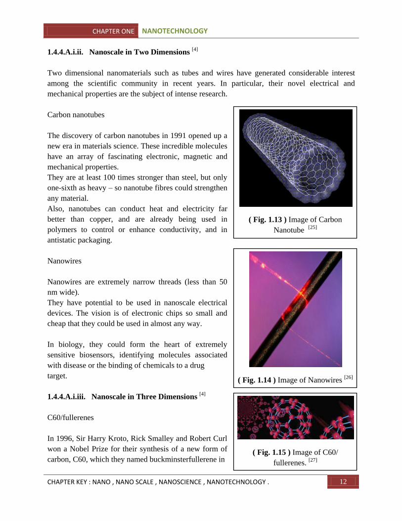
Two dimensional nanomaterials such as tubes and wires have generated considerable interest
among the scientific community in recent years. In particular, their novel electrical and
mechanical properties are the subject of intense research.
Carbon nanotubes
The discovery of carbon nanotubes in 1991 opened up a
new era in materials science. These incredible molecules
have an array of fascinating electronic, magnetic and
mechanical properties.
They are at least 100 times stronger than steel, but only
one-sixth as heavy – so nanotube fibres could strengthen
any material.
Also, nanotubes can conduct heat and electricity far
better than copper, and are already being used in
polymers to control or enhance conductivity, and in
antistatic packaging.
Nanowires
Nanowires are extremely narrow threads (less than 50
nm wide).
They have potential to be used in nanoscale electrical
devices. The vision is of electronic chips so small and
cheap that they could be used in almost any way.
In biology, they could form the heart of extremely
sensitive biosensors, identifying molecules associated
with disease or the binding of chemicals to a drug
target.
1.4.4.A.i.iii. Nanoscale in Three Dimensions [4]
C60/fullerenes
In 1996, Sir Harry Kroto, Rick Smalley and Robert Curl
won a Nobel Prize for their synthesis of a new form of
carbon, C60, which they named buckminsterfullerene in
( Fig. 1.13 ) Image of Carbon
Nanotube [25]
( Fig. 1.14 ) Image of Nanowires [26]
( Fig. 1.15 ) Image of C60/
fullerenes. [27]
CHAPTER ONE NANOTECHNOLOGY
CHAPTER KEY : NANO , NANO SCALE , NANOSCIENCE , NANOTECHNOLOGY . 13
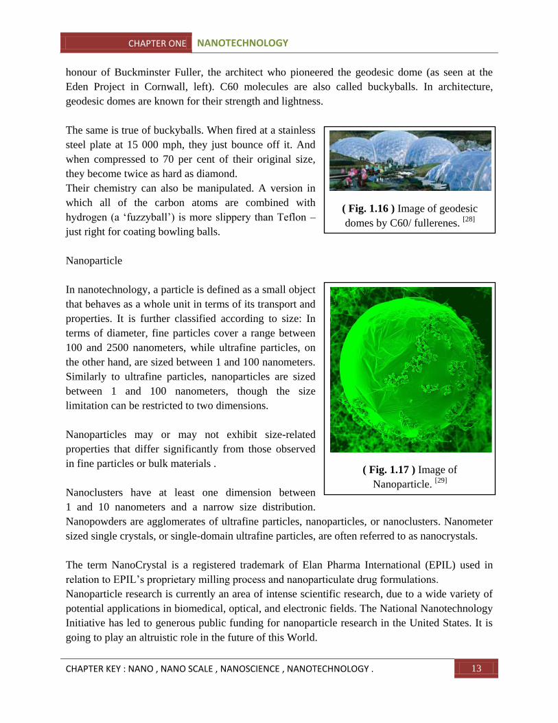
honour of Buckminster Fuller, the architect who pioneered the geodesic dome (as seen at the
Eden Project in Cornwall, left). C60 molecules are also called buckyballs. In architecture,
geodesic domes are known for their strength and lightness.
The same is true of buckyballs. When fired at a stainless
steel plate at 15 000 mph, they just bounce off it. And
when compressed to 70 per cent of their original size,
they become twice as hard as diamond.
Their chemistry can also be manipulated. A version in
which all of the carbon atoms are combined with
hydrogen (a „fuzzyball‟) is more slippery than Teflon –
just right for coating bowling balls.
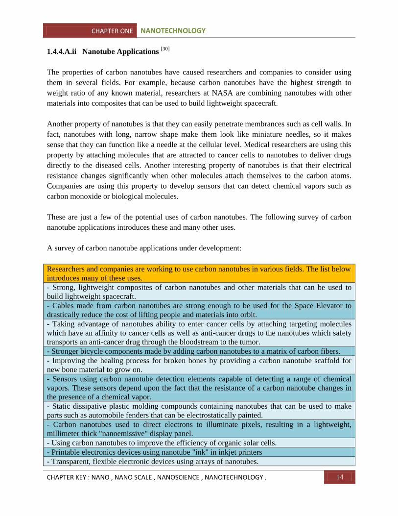
Nanoparticle
In nanotechnology, a particle is defined as a small object
that behaves as a whole unit in terms of its transport and
properties. It is further classified according to size: In
terms of diameter, fine particles cover a range between
100 and 2500 nanometers, while ultrafine particles, on
the other hand, are sized between 1 and 100 nanometers.
Similarly to ultrafine particles, nanoparticles are sized
between 1 and 100 nanometers, though the size
limitation can be restricted to two dimensions.
Nanoparticles may or may not exhibit size-related
properties that differ significantly from those observed
in fine particles or bulk materials .
Nanoclusters have at least one dimension between
1 and 10 nanometers and a narrow size distribution.
Nanopowders are agglomerates of ultrafine particles, nanoparticles, or nanoclusters. Nanometer
sized single crystals, or single-domain ultrafine particles, are often referred to as nanocrystals.
The term NanoCrystal is a registered trademark of Elan Pharma International (EPIL) used in
relation to EPIL‟s proprietary milling process and nanoparticulate drug formulations.
Nanoparticle research is currently an area of intense scientific research, due to a wide variety of
potential applications in biomedical, optical, and electronic fields. The National Nanotechnology
Initiative has led to generous public funding for nanoparticle research in the United States. It is
going to play an altruistic role in the future of this World.
( Fig. 1.16 ) Image of geodesic
domes by C60/ fullerenes. [28]
( Fig. 1.17 ) Image of
Nanoparticle. [29]
CHAPTER ONE NANOTECHNOLOGY
CHAPTER KEY : NANO , NANO SCALE , NANOSCIENCE , NANOTECHNOLOGY . 14
1.4.4.A.ii Nanotube Applications [30]
The properties of carbon nanotubes have caused researchers and companies to consider using
them in several fields. For example, because carbon nanotubes have the highest strength to
weight ratio of any known material, researchers at NASA are combining nanotubes with other
materials into composites that can be used to build lightweight spacecraft.
Another property of nanotubes is that they can easily penetrate membrances such as cell walls. In
fact, nanotubes with long, narrow shape make them look like miniature needles, so it makes
sense that they can function like a needle at the cellular level. Medical researchers are using this
property by attaching molecules that are attracted to cancer cells to nanotubes to deliver drugs
directly to the diseased cells. Another interesting property of nanotubes is that their electrical
resistance changes significantly when other molecules attach themselves to the carbon atoms.
Companies are using this property to develop sensors that can detect chemical vapors such as
carbon monoxide or biological molecules.
These are just a few of the potential uses of carbon nanotubes. The following survey of carbon
nanotube applications introduces these and many other uses.
A survey of carbon nanotube applications under development:
Researchers and companies are working to use carbon nanotubes in various fields. The list below
introduces many of these uses.
- Strong, lightweight composites of carbon nanotubes and other materials that can be used to
build lightweight spacecraft.
- Cables made from carbon nanotubes are strong enough to be used for the Space Elevator to
drastically reduce the cost of lifting people and materials into orbit.
- Taking advantage of nanotubes ability to enter cancer cells by attaching targeting molecules
which have an affinity to cancer cells as well as anti-cancer drugs to the nanotubes which safety
transports an anti-cancer drug through the bloodstream to the tumor.
- Stronger bicycle components made by adding carbon nanotubes to a matrix of carbon fibers.
- Improving the healing process for broken bones by providing a carbon nanotube scaffold for
new bone material to grow on.
- Sensors using carbon nanotube detection elements capable of detecting a range of chemical
vapors. These sensors depend upon the fact that the resistance of a carbon nanotube changes in
the presence of a chemical vapor.
- Static dissipative plastic molding compounds containing nanotubes that can be used to make
parts such as automobile fenders that can be electrostatically painted.
- Carbon nanotubes used to direct electrons to illuminate pixels, resulting in a lightweight,
millimeter thick "nanoemissive" display panel.
- Using carbon nanotubes to improve the efficiency of organic solar cells.
- Printable electronics devices using nanotube "ink" in inkjet printers
- Transparent, flexible electronic devices using arrays of nanotubes.
CHAPTER ONE NANOTECHNOLOGY
CHAPTER KEY : NANO , NANO SCALE , NANOSCIENCE , NANOTECHNOLOGY . 15
1.4.4.A.iii. Nanoparticle Applications [30]
The properties of many conventional materials change when formed from nanoparticles. This is
typically because nanoparticles have a greater surface area per weight than larger particles; they
are therefore more reactive to certain other molecules.
A survey of nanoparticle applications under development:
Nanoparticles are used in many fields, the list below introduces many of those uses.
- Pallidium nanoparticles used in chemical vapor sensors to detect hydrogen gas.
- Quantum Dots (crystalline nanoparticles) that identify the location of cancer cells in the body.
- Iron nanoparticles used to clean up carbon tetrachloride pollution in ground water
- Silicate nanoparticles used to provide a barrier to gasses (for example oxygen), or moisture in a
plastic film used for packaging. This could reduce the possibility of food spoiling or drying out.
- Zinc oxide nanoparticles dispersed in industrial coatings to protect wood, plastic and textiles
from exposure to UV rays.
- Silicon dioxide crystalline nanoparticles filling gaps between carbon fibers strengthen tennis
racquets.
- Silver nanoparticles in fabric that kill bacteria making clothing odor-resistant.
- Titanium oxide nanoparticles used as a photocatalyst to remove germs and other pollutants
from air
- Manganese oxide nanoparticles used as a catalyst for removal of volatile organic compounds in
industrial air emissions
- Zinc oxide nano-wires used as detection elements in sensors capable of detecting a range of
chemical vapors.
1.4.4.B. Bottom-up approaches [12]
These seek to arrange smaller components into more
complex assemblies.
- DNA nanotechnology utilizes the specificity of
Watson-Crick basepairing to construct well-defined
structures out of DNA and other nucleic acids.
- Approaches from the field of "classical" chemical
synthesis also aim at designing molecules with well-
defined shape (e.g. bis-peptides)
- More generally, molecular self-assembly seeks to use concepts of supramolecular chemistry,
and molecular recognition in particular, to cause single-molecule components to automatically
arrange themselves into some useful conformation.
( Fig. 1.18 ) Sarfus image of a DNA
biochip elaborated by bottom-up
approach. [12]
CHAPTER ONE NANOTECHNOLOGY
CHAPTER KEY : NANO , NANO SCALE , NANOSCIENCE , NANOTECHNOLOGY . 16
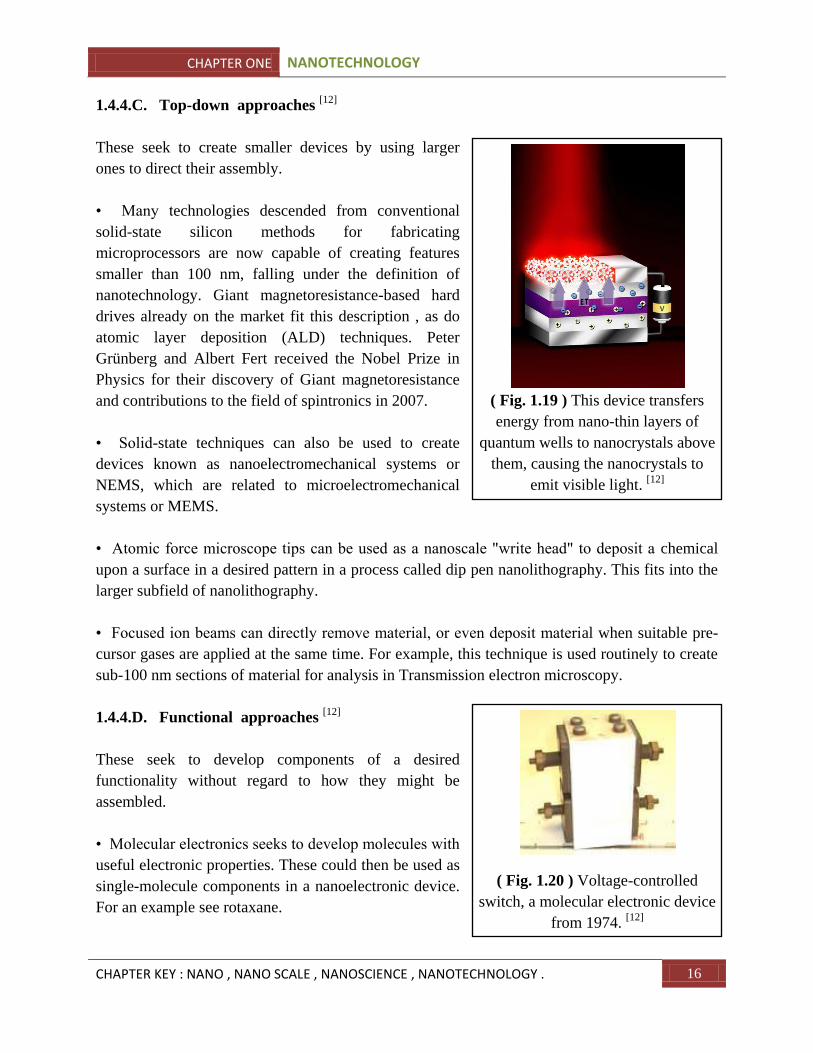
1.4.4.C. Top-down approaches [12]
These seek to create smaller devices by using larger
ones to direct their assembly.
• Many technologies descended from conventional
solid-state silicon methods for fabricating
microprocessors are now capable of creating features
smaller than 100 nm, falling under the definition of
nanotechnology. Giant magnetoresistance-based hard
drives already on the market fit this description , as do
atomic layer deposition (ALD) techniques. Peter
Grünberg and Albert Fert received the Nobel Prize in
Physics for their discovery of Giant magnetoresistance
and contributions to the field of spintronics in 2007.
• Solid-state techniques can also be used to create
devices known as nanoelectromechanical systems or
NEMS, which are related to microelectromechanical
systems or MEMS.
• Atomic force microscope tips can be used as a nanoscale "write head" to deposit a chemical
upon a surface in a desired pattern in a process called dip pen nanolithography. This fits into the
larger subfield of nanolithography.
• Focused ion beams can directly remove material, or even deposit material when suitable pre-
cursor gases are applied at the same time. For example, this technique is used routinely to create
sub-100 nm sections of material for analysis in Transmission electron microscopy.
1.4.4.D. Functional approaches [12]
These seek to develop components of a desired
functionality without regard to how they might be
assembled.
• Molecular electronics seeks to develop molecules with
useful electronic properties. These could then be used as
single-molecule components in a nanoelectronic device.
For an example see rotaxane.
( Fig. 1.19 ) This device transfers
energy from nano-thin layers of
quantum wells to nanocrystals above
them, causing the nanocrystals to
emit visible light. [12]
( Fig. 1.20 ) Voltage-controlled
switch, a molecular electronic device
from 1974. [12]
CHAPTER ONE NANOTECHNOLOGY
CHAPTER KEY : NANO , NANO SCALE , NANOSCIENCE , NANOTECHNOLOGY . 17
• Synthetic chemical methods can also be used to create
what forensics call synthetic molecular motors, such as
in a so-called nanocar.
1.4.4.E. Speculative [12]
These subfields seek to anticipate what inventions
nanotechnology might yield, or attempt to propose an
agenda along which inquiry might progress. These often
take a big-picture view of nanotechnology, with more
emphasis on its societal implications than the details of
how such inventions could actually be created.
• Molecular nanotechnology is a proposed approach
which involves manipulating single molecules in finely
controlled, deterministic ways. This is more theoretical
than the other subfields and is beyond current
capabilities.
• Nanorobotics centers on self-sufficient machines of
some functionality operating at the nanoscale. There are
hopes for applying nanorobots in medicine , but it may
not be easy to do such a thing because of the several
drawbacks of such devices. Nevertheless, progress on
innovative materials and methodologies has been
demonstrated with some patents granted about new
nanomanufacturing devices for future commercial
applications, which also progressively helps in the
development towards nanorobots with the use of
embedded nanobioelectronics concept.
• Programmable matter based on artificial atoms seeks
to design materials whose properties can be easily,
reversibly and externally controlled.
• Due to the popularity and media exposure of the term
nanotechnology, the words picotechnology and
femtotechnology have been coined in analogy to it,
although these are only used rarely and informally.
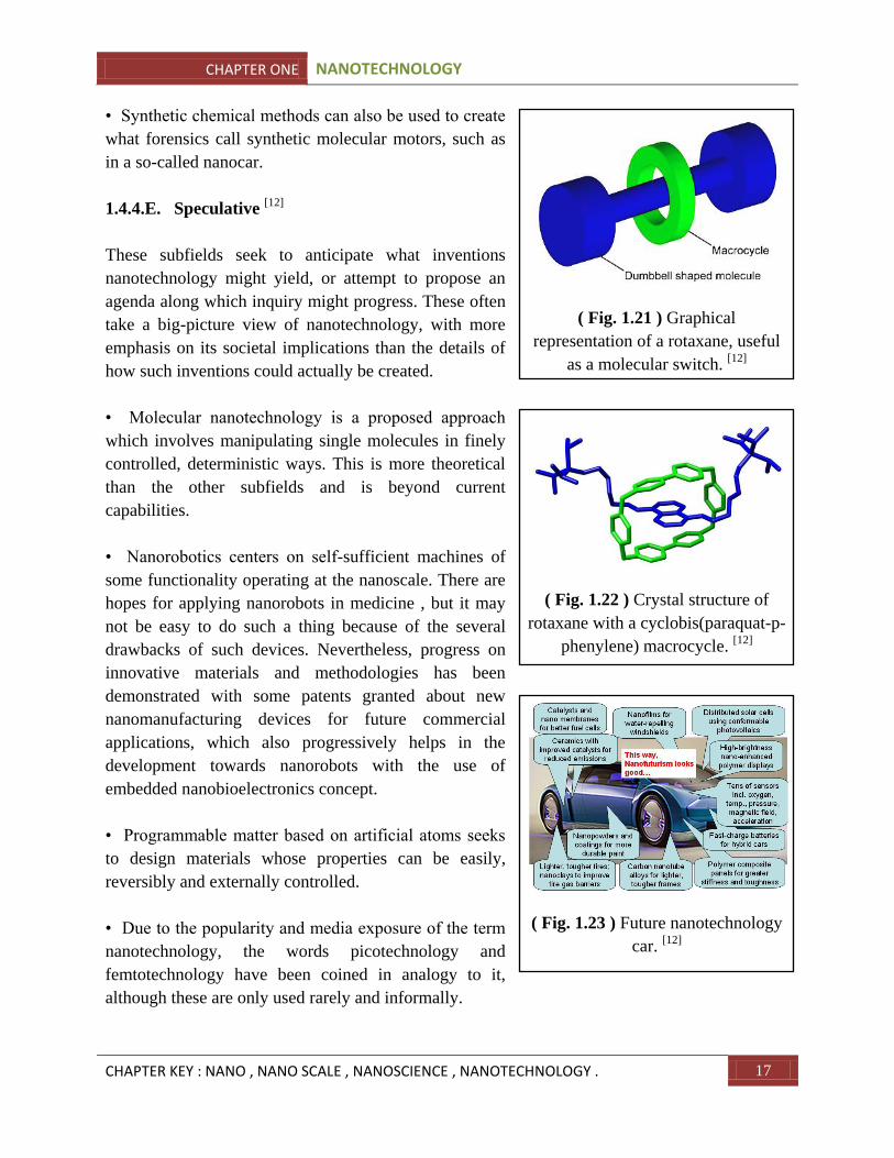
( Fig. 1.21 ) Graphical
representation of a rotaxane, useful
as a molecular switch. [12]
( Fig. 1.23 ) Future nanotechnology
car. [12]
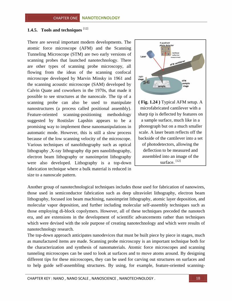
( Fig. 1.22 ) Crystal structure of
rotaxane with a cyclobis(paraquat-p-
phenylene) macrocycle. [12]
CHAPTER ONE NANOTECHNOLOGY
CHAPTER KEY : NANO , NANO SCALE , NANOSCIENCE , NANOTECHNOLOGY . 18
1.4.5. Tools and techniques [12]
There are several important modern developments. The
atomic force microscope (AFM) and the Scanning
Tunneling Microscope (STM) are two early versions of
scanning probes that launched nanotechnology. There
are other types of scanning probe microscopy, all
flowing from the ideas of the scanning confocal
microscope developed by Marvin Minsky in 1961 and
the scanning acoustic microscope (SAM) developed by
Calvin Quate and coworkers in the 1970s, that made it
possible to see structures at the nanoscale. The tip of a
scanning probe can also be used to manipulate
nanostructures (a process called positional assembly).
Feature-oriented scanning-positioning methodology
suggested by Rostislav Lapshin appears to be a
promising way to implement these nanomanipulations in
automatic mode. However, this is still a slow process
because of the low scanning velocity of the microscope.
Various techniques of nanolithography such as optical
lithography ,X-ray lithography dip pen nanolithography,
electron beam lithography or nanoimprint lithography
were also developed. Lithography is a top-down
fabrication technique where a bulk material is reduced in
size to a nanoscale pattern.
Another group of nanotechnological techniques includes those used for fabrication of nanowires,
those used in semiconductor fabrication such as deep ultraviolet lithography, electron beam
lithography, focused ion beam machining, nanoimprint lithography, atomic layer deposition, and
molecular vapor deposition, and further including molecular self-assembly techniques such as
those employing di-block copolymers. However, all of these techniques preceded the nanotech
era, and are extensions in the development of scientific advancements rather than techniques
which were devised with the sole purpose of creating nanotechnology and which were results of
nanotechnology research.
The top-down approach anticipates nanodevices that must be built piece by piece in stages, much
as manufactured items are made. Scanning probe microscopy is an important technique both for
the characterization and synthesis of nanomaterials. Atomic force microscopes and scanning
tunneling microscopes can be used to look at surfaces and to move atoms around. By designing
different tips for these microscopes, they can be used for carving out structures on surfaces and
to help guide self-assembling structures. By using, for example, feature-oriented scanning-
( Fig. 1.24 ) Typical AFM setup. A
microfabricated cantilever with a
sharp tip is deflected by features on
a sample surface, much like in a
phonograph but on a much smaller
scale. A laser beam reflects off the
backside of the cantilever into a set
of photodetectors, allowing the
deflection to be measured and
assembled into an image of the
surface. [12]
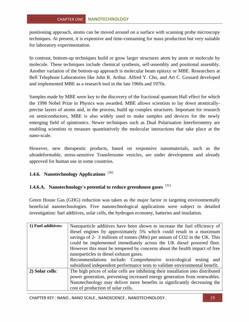
CHAPTER ONE NANOTECHNOLOGY
CHAPTER KEY : NANO , NANO SCALE , NANOSCIENCE , NANOTECHNOLOGY . 19
positioning approach, atoms can be moved around on a surface with scanning probe microscopy
techniques. At present, it is expensive and time-consuming for mass production but very suitable
for laboratory experimentation.
In contrast, bottom-up techniques build or grow larger structures atom by atom or molecule by
molecule. These techniques include chemical synthesis, self-assembly and positional assembly.
Another variation of the bottom-up approach is molecular beam epitaxy or MBE. Researchers at
Bell Telephone Laboratories like John R. Arthur. Alfred Y. Cho, and Art C. Gossard developed
and implemented MBE as a research tool in the late 1960s and 1970s.
Samples made by MBE were key to the discovery of the fractional quantum Hall effect for which
the 1998 Nobel Prize in Physics was awarded. MBE allows scientists to lay down atomically-
precise layers of atoms and, in the process, build up complex structures. Important for research
on semiconductors, MBE is also widely used to make samples and devices for the newly
emerging field of spintronics. Newer techniques such as Dual Polarisation Interferometry are
enabling scientists to measure quantitatively the molecular interactions that take place at the
nano-scale.
However, new therapeutic products, based on responsive nanomaterials, such as the
ultradeformable, stress-sensitive Transfersome vesicles, are under development and already
approved for human use in some countries.
1.4.6. Nanotechnology Applications [30]
1.4.6.A. Nanotechnology's potential to reduce greenhouse gases [31]
Green House Gas (GHG) reduction was taken as the major factor in targeting environmentally
beneficial nanotechnologies. Five nanotechnological applications were subject to detailed
investigation: fuel additives, solar cells, the hydrogen economy, batteries and insulation.
1) Fuel additives: Nanoparticle additives have been shown to increase the fuel efficiency of
diesel engines by approximately 5% which could result in a maximum
savinga of 2‐ 3 millions of tonnes (Mte) per annum of CO2 in the UK. This
could be implemented immediately across the UK diesel powered fleet.
However this must be tempered by concerns about the health impact of free
nanoparticles in diesel exhaust gases.
Recommendations include: Comprehensive toxicological testing and
subsidized independent performance tests to validate environmental benefit.
2) Solar cells: The high prices of solar cells are inhibiting their installation into distributed
power generation, preventing increased energy generation from renewables.
Nanotechnology may deliver more benefits in significantly decreasing the
cost of production of solar cells.
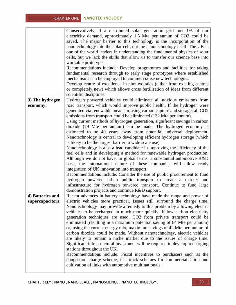
CHAPTER ONE NANOTECHNOLOGY
CHAPTER KEY : NANO , NANO SCALE , NANOSCIENCE , NANOTECHNOLOGY . 20
Conservatively, if a distributed solar generation grid met 1% of our
electricity demand, approximately 1.5 Mte per annum of CO2 could be
saved. The major barrier to this technology is the incorporation of the
nanotechnology into the solar cell, not the nanotechnology itself. The UK is
one of the world leaders in understanding the fundamental physics of solar
cells, but we lack the skills that allow us to transfer our science base into
workable prototypes.
Recommendations include: Develop programmes and facilities for taking
fundamental research through to early stage prototypes where established
mechanisms can be employed to commercialise new technologies.
Develop centre of excellence in photovoltaics (either from existing centres
or completely new) which allows cross fertilisation of ideas from different
scientific disciplines.
3) The hydrogen
economy:
Hydrogen powered vehicles could eliminate all noxious emissions from
road transport, which would improve public health. If the hydrogen were
generated via renewable means or using carbon capture and storage, all CO2
emissions from transport could be eliminated (132 Mte per annum).
Using current methods of hydrogen generation, significant savings in carbon
dioxide (79 Mte per annum) can be made. The hydrogen economy is
estimated to be 40 years away from potential universal deployment.
Nanotechnology is central to developing efficient hydrogen storage (which
is likely to be the largest barrier to wide scale use).
Nanotechnology is also a lead candidate in improving the efficiency of the
fuel cells and in developing a method for renewable hydrogen production.
Although we do not have, in global terms, a substantial automotive R&D
base, the international nature of these companies will allow ready
integration of UK innovation into transport.
Recommendations include: Consider the use of public procurement to fund
hydrogen powered urban public transport to create a market and
infrastructure for hydrogen powered transport. Continue to fund large
demonstration projects and continue R&D support.
4) Batteries and
supercapacitors:
Recent advances in battery technology have made the range and power of
electric vehicles more practical. Issues still surround the charge time.
Nanotechnology may provide a remedy to this problem by allowing electric
vehicles to be recharged in much more quickly. If low carbon electricity
generation techniques are used, CO2 from private transport could be
eliminated (resulting in a maximum potential saving of 64 Mte per annum)
or, using the current energy mix, maximum savings of 42 Mte per annum of
carbon dioxide could be made. Without nanotechnology, electric vehicles
are likely to remain a niche market due to the issues of charge time.
Significant infrastructural investment will be required to develop recharging
stations throughout the UK.
Recommendations include: Fiscal incentives to purchasers such as the
congestion charge scheme, fast track schemes for commercialisation and
cultivation of links with automotive multinationals.
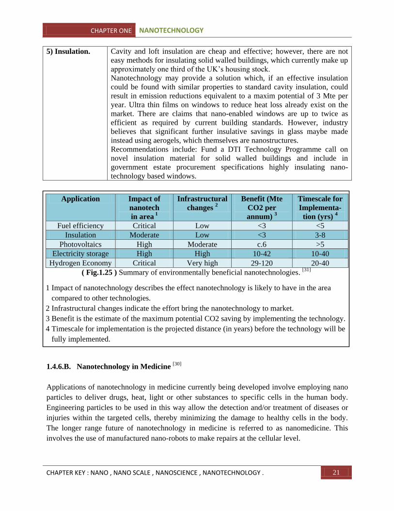
CHAPTER ONE NANOTECHNOLOGY
CHAPTER KEY : NANO , NANO SCALE , NANOSCIENCE , NANOTECHNOLOGY . 21
5) Insulation.
Cavity and loft insulation are cheap and effective; however, there are not
easy methods for insulating solid walled buildings, which currently make up
approximately one third of the UK‟s housing stock.
Nanotechnology may provide a solution which, if an effective insulation
could be found with similar properties to standard cavity insulation, could
result in emission reductions equivalent to a maxim potential of 3 Mte per
year. Ultra thin films on windows to reduce heat loss already exist on the
market. There are claims that nano-enabled windows are up to twice as
efficient as required by current building standards. However, industry
believes that significant further insulative savings in glass maybe made
instead using aerogels, which themselves are nanostructures.
Recommendations include: Fund a DTI Technology Programme call on
novel insulation material for solid walled buildings and include in
government estate procurement specifications highly insulating nano-
technology based windows.
1.4.6.B. Nanotechnology in Medicine [30]
Applications of nanotechnology in medicine currently being developed involve employing nano
particles to deliver drugs, heat, light or other substances to specific cells in the human body.
Engineering particles to be used in this way allow the detection and/or treatment of diseases or
injuries within the targeted cells, thereby minimizing the damage to healthy cells in the body.
The longer range future of nanotechnology in medicine is referred to as nanomedicine. This
involves the use of manufactured nano-robots to make repairs at the cellular level.
Application Impact of
nanotech
in area 1
Infrastructural
changes 2
Benefit (Mte
CO2 per
annum) 3
Timescale for
Implementa-
tion (yrs) 4
Fuel efficiency Critical Low <3 <5
Insulation Moderate Low <3 3‐8
Photovoltaics High Moderate c.6 >5
Electricity storage High High 10‐42 10‐40
Hydrogen Economy Critical Very high 29‐120 20‐40
( Fig.1.25 ) Summary of environmentally beneficial nanotechnologies. [31]
1 Impact of nanotechnology describes the effect nanotechnology is likely to have in the area
compared to other technologies.
2 Infrastructural changes indicate the effort bring the nanotechnology to market.
3 Benefit is the estimate of the maximum potential CO2 saving by implementing the technology.
4 Timescale for implementation is the projected distance (in years) before the technology will be
fully implemented.
CHAPTER ONE NANOTECHNOLOGY
CHAPTER KEY : NANO , NANO SCALE , NANOSCIENCE , NANOTECHNOLOGY . 22
1.4.6.C. Nanotechnology in Electronics [30]
How can nanoelectronics improve the capabilities of electronic components?
Nanoelectronics holds some answers for how we might increase the capabilities of electronic
devices while we reduce their weight and power consumption.
Some of the nanoelectronics areas under development, which you can explore in more detail by
following the links provided in the next section, include:
Improving display screens on electronic devices. This involves reducing power
consumption while decreasing the weight and thickness of the screens.
Increasing the density of memory chips. Researchers are developing a type of memory
chip with a projected density of one terabyte of memory per square inch or greater.
Reducing the size of transistors used in integrated circuits.
1.4.6.D. Nanotechnology and Space [30]
Nanotechnology may hold the key to making space-flight more practical. Advancements in
nanomaterials make lightweight solar sails and a cable for the space elevator possible. By
significantly reducing the amount of rocket fuel required, these advances could lower the cost of
reaching orbit and traveling in space. In addition, new materials combined with nanosensors and
nanorobots could improve the performance of spaceships, spacesuits, and the equipment used to
explore planets and moons, making nanotechnology an important part of the „final frontier.
1.4.6.E. Air Pollution and Nanotechnology [30]
How can nanotechnology reduce air pollution?
There are two major ways in which nanotechnology is being used to reduce air pollution:
catalysts, which are currently in use and constantly being improved upon; and nano-structured
membranes, which are under development.
Catalysts can be used to enable a chemical reaction (which changes one type of molecule to
another) at lower temperatures or make the reaction more effective. Nanotechnology can
improve the performance and cost of catalysts used to transform vapors escaping from cars or
industrial plants into harmless gases.That's because catalysts made from nanoparticles have a
greater surface area to interact with the reacting chemicals than catalysts made from larger
particles. The larger surface area allows more chemicals to interact with the catalyst
simultaneously, which makes the catalyst more effective. Nanostructured membranes, on the
other hand, are being developed to separate carbon dioxide from industrial plant exhaust streams.
The plan is to create a method that can be implemented in any power plant without expensive
retrofitting.

CHAPTER ONE NANOTECHNOLOGY
CHAPTER KEY : NANO , NANO SCALE , NANOSCIENCE , NANOTECHNOLOGY . 23
1.4.6.F. Water Pollution and Nanotechnology [30]
How can nanotechnology be used to reduce water pollution?
Nanotechnology is being used to develop solutions to three very different problems in water
quality.
One challenge is the removal of industrial water pollution, such as a cleaning solvent called
TCE, from ground water. Nanoparticles can be used to convert the contaminating chemical
through a chemical reaction to make it harmless. Studies have shown that this method can be
used successfully to reach contaminates dispersed in underground ponds and at much lower cost
than methods which require pumping the water out of the ground for treatment.
The challenge is the removal of salt or metals from water. A deionization method using
electrodes composed of nano-sized fibers shows promise for reducing the cost and energy
requirements of turning salt water into drinking water.
The third problem concerns the fact that standard filters do not work on virus cells. A filter only
a few nanometers in diameter is currently being developed that should be capable of removing
virus cells from water.
1.4.6.G. Nanotechnology and Chemical Sensors [30]
Nanotechnology can enable sensors to detect very small amounts of chemical vapors. Various
types of detecting elements, such as carbon nanotubes, zinc oxide nanowires or palladium
nanoparticles can be used in nanotechnology-based sensors. Because of the small size of
nanotubes, nanowires, or nanoparticles, a few gas molecules are sufficient to change the
electrical properties of the sensing elements. This allows the detection of a very low
concentration of chemical vapors.
1.4.6.H. Nanotechnology and Fabric [30]
How can nanotechnology improve fabric?
Making composite fabric with nano-sized particles or fibers allows improvement of fabric
properties without a significant increase in weight, thickness, or stiffness as might have been the
case with previously-used techniques.
For example incorporating nano-whiskers into fabric used to make pants produces a lightweight
water and stain repellent material.
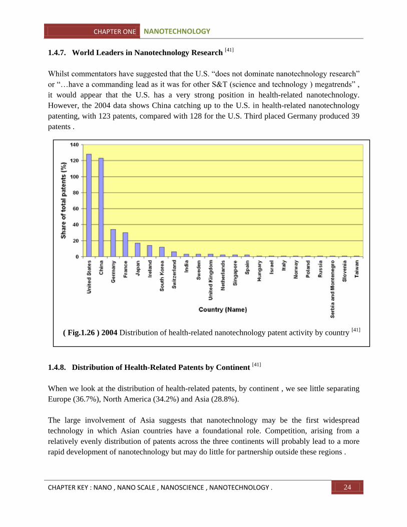
CHAPTER ONE NANOTECHNOLOGY
CHAPTER KEY : NANO , NANO SCALE , NANOSCIENCE , NANOTECHNOLOGY . 24
1.4.7. World Leaders in Nanotechnology Research [41]
Whilst commentators have suggested that the U.S. “does not dominate nanotechnology research”
or “…have a commanding lead as it was for other S&T (science and technology ) megatrends” ,
it would appear that the U.S. has a very strong position in health-related nanotechnology.
However, the 2004 data shows China catching up to the U.S. in health-related nanotechnology
patenting, with 123 patents, compared with 128 for the U.S. Third placed Germany produced 39
patents .
1.4.8. Distribution of Health-Related Patents by Continent [41]
When we look at the distribution of health-related patents, by continent , we see little separating
Europe (36.7%), North America (34.2%) and Asia (28.8%).
The large involvement of Asia suggests that nanotechnology may be the first widespread
technology in which Asian countries have a foundational role. Competition, arising from a
relatively evenly distribution of patents across the three continents will probably lead to a more
rapid development of nanotechnology but may do little for partnership outside these regions .
( Fig.1.26 ) 2004 Distribution of health-related nanotechnology patent activity by country [41]
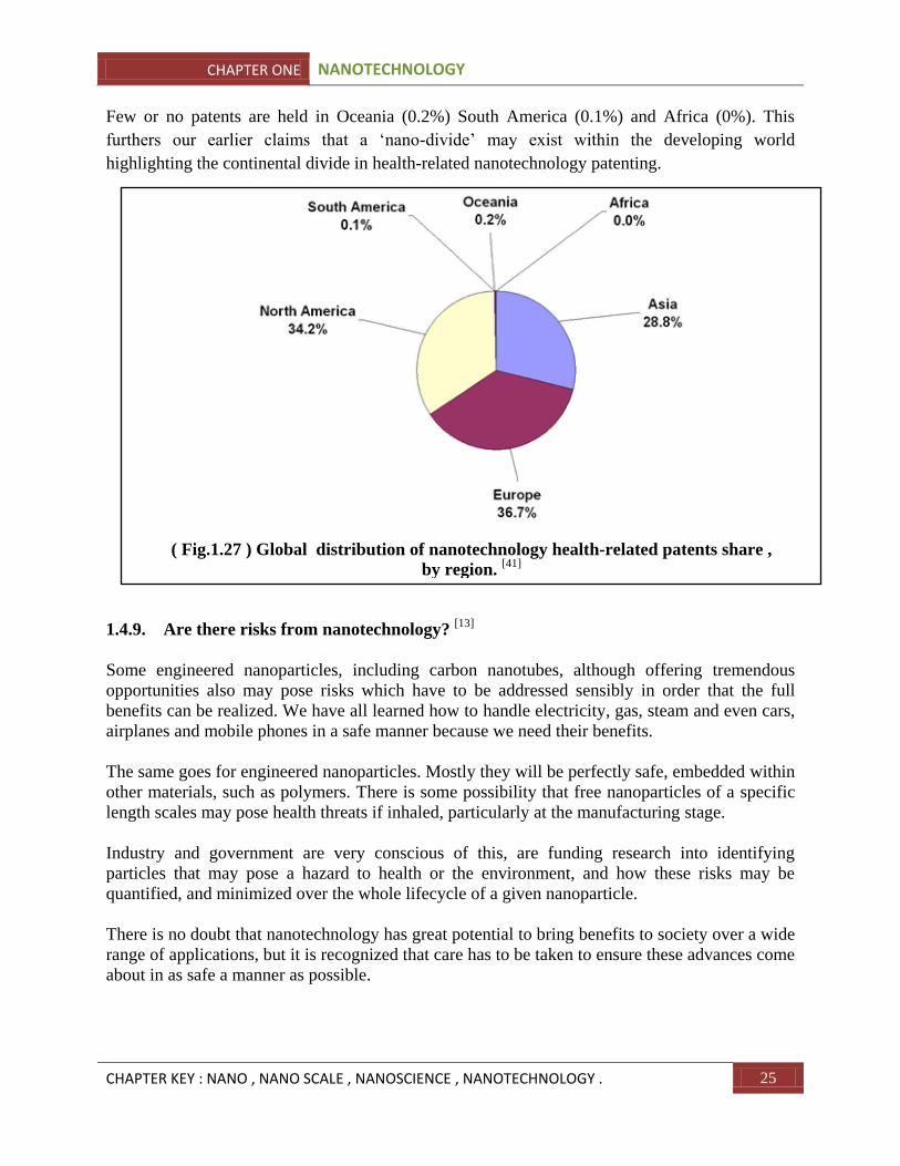
CHAPTER ONE NANOTECHNOLOGY
CHAPTER KEY : NANO , NANO SCALE , NANOSCIENCE , NANOTECHNOLOGY . 25
Few or no patents are held in Oceania (0.2%) South America (0.1%) and Africa (0%). This
furthers our earlier claims that a „nano-divide‟ may exist within the developing world
highlighting the continental divide in health-related nanotechnology patenting.
1.4.9. Are there risks from nanotechnology? [13]
Some engineered nanoparticles, including carbon nanotubes, although offering tremendous
opportunities also may pose risks which have to be addressed sensibly in order that the full
benefits can be realized. We have all learned how to handle electricity, gas, steam and even cars,
airplanes and mobile phones in a safe manner because we need their benefits.
The same goes for engineered nanoparticles. Mostly they will be perfectly safe, embedded within
other materials, such as polymers. There is some possibility that free nanoparticles of a specific
length scales may pose health threats if inhaled, particularly at the manufacturing stage.
Industry and government are very conscious of this, are funding research into identifying
particles that may pose a hazard to health or the environment, and how these risks may be
quantified, and minimized over the whole lifecycle of a given nanoparticle.
There is no doubt that nanotechnology has great potential to bring benefits to society over a wide
range of applications, but it is recognized that care has to be taken to ensure these advances come
about in as safe a manner as possible.
( Fig.1.27 ) Global distribution of nanotechnology health-related patents share ,
by region. [41]
CHAPTER ONE NANOTECHNOLOGY
CHAPTER KEY : NANO , NANO SCALE , NANOSCIENCE , NANOTECHNOLOGY . 26
It would be difficult to deny the potential benefits of nanotechnology and stop development of
research related to it since it has already begun to penetrate many different fields of research.
However, nanotechnology can be developed using guidelines to insure that the technology does
not become too potentially harmful. As with any new technology, it is impossible to stop every
well funded organization which may seek to develop the technology for harmful purposes.
However, if the researchers in this field put together an ethical set of guidelines (e.g., Molecular
Nanotechnology Guidelines6) and follow them, then we should be able to develop
nanotechnology safely while still reaping its promised benefits.
1.5. CONCLUSION [14]

CHAPTER TWO
NANOARCHITECTURE
N A N O A R C H I T E C T U R E
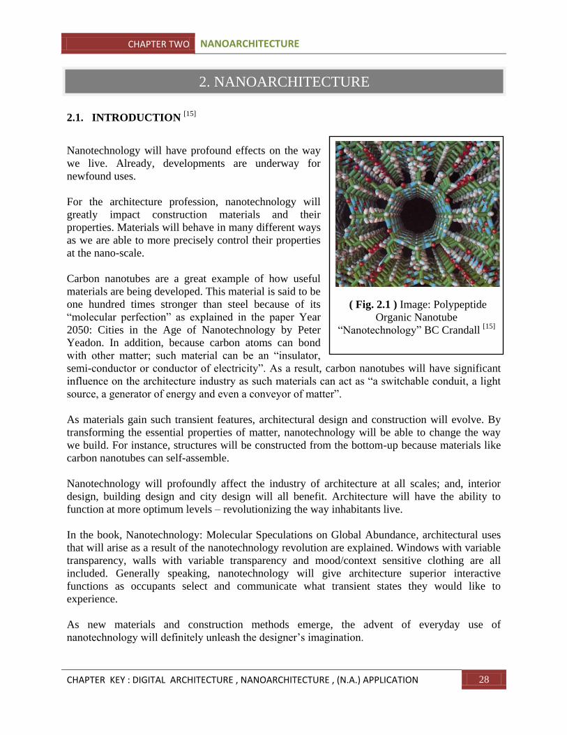
CHAPTER TWO NANOARCHITECTURE
CHAPTER KEY : DIGITAL ARCHITECTURE , NANOARCHITECTURE , (N.A.) APPLICATION 28
2.1. INTRODUCTION [15]
Nanotechnology will have profound effects on the way
we live. Already, developments are underway for
newfound uses.
For the architecture profession, nanotechnology will
greatly impact construction materials and their
properties. Materials will behave in many different ways
as we are able to more precisely control their properties
at the nano-scale.
Carbon nanotubes are a great example of how useful
materials are being developed. This material is said to be
one hundred times stronger than steel because of its
“molecular perfection” as explained in the paper Year
2050: Cities in the Age of Nanotechnology by Peter
Yeadon. In addition, because carbon atoms can bond
with other matter; such material can be an “insulator,
semi-conductor or conductor of electricity”. As a result, carbon nanotubes will have significant
influence on the architecture industry as such materials can act as “a switchable conduit, a light
source, a generator of energy and even a conveyor of matter”.
As materials gain such transient features, architectural design and construction will evolve. By
transforming the essential properties of matter, nanotechnology will be able to change the way
we build. For instance, structures will be constructed from the bottom-up because materials like
carbon nanotubes can self-assemble.
Nanotechnology will profoundly affect the industry of architecture at all scales; and, interior
design, building design and city design will all benefit. Architecture will have the ability to
function at more optimum levels – revolutionizing the way inhabitants live.
In the book, Nanotechnology: Molecular Speculations on Global Abundance, architectural uses
that will arise as a result of the nanotechnology revolution are explained. Windows with variable
transparency, walls with variable transparency and mood/context sensitive clothing are all
included. Generally speaking, nanotechnology will give architecture superior interactive
functions as occupants select and communicate what transient states they would like to
experience.
As new materials and construction methods emerge, the advent of everyday use of
nanotechnology will definitely unleash the designer‟s imagination.
2. NANOARCHITECTURE
( Fig. 2.1 ) Image: Polypeptide
Organic Nanotube
“Nanotechnology” BC Crandall [15]

CHAPTER TWO NANOARCHITECTURE
CHAPTER KEY : DIGITAL ARCHITECTURE , NANOARCHITECTURE , (N.A.) APPLICATION 29
CG artists provide other-worldly inspiration for
architecture. Inspiration comes from many places but
more often than not, it comes from the inspired. Perhaps
this is why CGSociety and NVIDIA held their
artspace|Architecture and Landscape Digital Design
competition earlier this year.While more typically
associated with the worlds of gaming and cinematic
effects, hundreds of CG designers had a go at showing
us what future and other-worldly landscapes could look
like, if we just used a little more imagination. More and
more, gaming is about telling a story and the more
dramatic the better.
The NVArt competition allowed digital artists to inject
life into stationary structures, adding narrative to help
define the structures and to stretch the technical
boundaries of design. But while by today's abilities
the designs are unlikely to reach fruition, they also
exhibit a strong regard for contemporary architectural
considerations.
In the third place, citing inspiration from Zaha Hadid, is
'Mega Village 2108'. This spiral design reaches up from
a single-point base, defying gravity as it heads
horizontally across a valley-scape. The design's artist
explains that advances in technology could allow similar
structures to exist in the future: “In the near future new
materials like carbon nano tubes make new kinds of
buildings possible, 50 times stronger and many times
lighter than steel.
"This mega village houses half a
million people , With a very small footprint and the
majority of travel in and out done by air, this building
has very little negative impact in the surrounding
environment,” says Xdroo. One of several designs which
did not receive a prize but did receive a notable mention
was 'Solaric Glass Anemone Structure II'. This design is
certainly one of the most awe-inspiring, bestowing a
wonderfully realistic sheen onto the dark glass clover
2.2. DIGITAL ARCHITECTURE [16]
( Fig. 2.2 ) 1st place: “Complex at
the Centre of the Universe” by
Staszek Marek, Poland. [16]
( Fig. 2.3 ) 2nd Place : The Great
Bayan by Sergey Skachkov
RUSSIA. [16]
( Fig. 2.4 ) 3rd place : Mega Village
2108 by Andrew Barton GREAT
BRITAIN. [16]
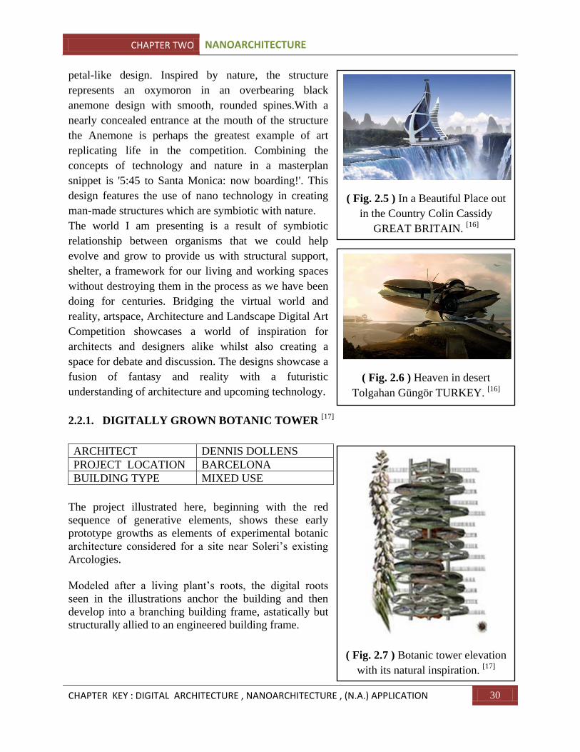
CHAPTER TWO NANOARCHITECTURE
CHAPTER KEY : DIGITAL ARCHITECTURE , NANOARCHITECTURE , (N.A.) APPLICATION 30
petal-like design. Inspired by nature, the structure
represents an oxymoron in an overbearing black
anemone design with smooth, rounded spines.With a
nearly concealed entrance at the mouth of the structure
the Anemone is perhaps the greatest example of art
replicating life in the competition.
Combining the
concepts of technology and nature in a masterplan
snippet is '5:45 to Santa Monica: now boarding!'. This
design features the use of nano technology in creating
man-made structures which are symbiotic with nature.
The world I am presenting is a result of symbiotic
relationship between organisms that we could help
evolve and grow to provide us with structural support,
shelter, a framework for our living and working spaces
without destroying them in the process as we have been
doing for centuries. Bridging the virtual world and
reality, artspace, Architecture and Landscape Digital Art
Competition showcases a world of inspiration for
architects and designers alike whilst also creating a
space for debate and discussion. The designs showcase a
fusion of fantasy and reality with a futuristic
understanding of architecture and upcoming technology.
2.2.1. DIGITALLY GROWN BOTANIC TOWER [17]
ARCHITECT DENNIS DOLLENS
PROJECT LOCATION BARCELONA
BUILDING TYPE MIXED USE
The project illustrated here, beginning with the red
sequence of generative elements, shows these early
prototype growths as elements of experimental botanic
architecture considered for a site near Soleri‟s existing
Arcologies.
Modeled after a living plant‟s roots, the digital roots
seen in the illustrations anchor the building and then
develop into a branching building frame, astatically but
structurally allied to an engineered building frame.
( Fig. 2.5 ) In a Beautiful Place out
in the Country Colin Cassidy
GREAT BRITAIN. [16]
( Fig. 2.6 ) Heaven in desert
Tolgahan Güngör TURKEY. [16]
( Fig. 2.7 ) Botanic tower elevation
with its natural inspiration. [17]
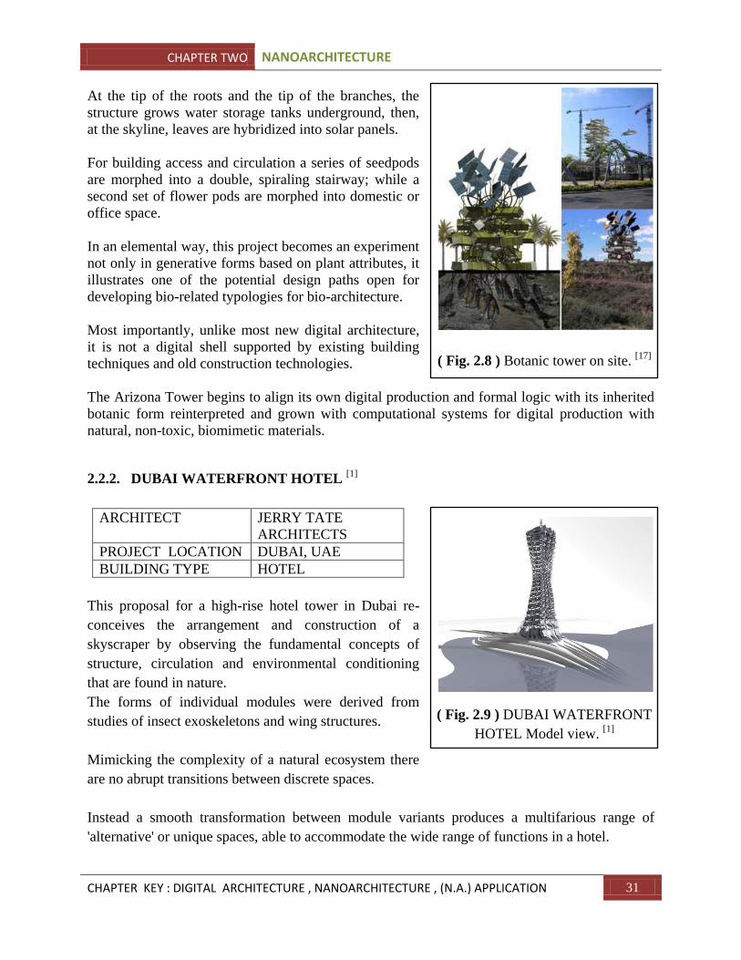
CHAPTER TWO NANOARCHITECTURE
CHAPTER KEY : DIGITAL ARCHITECTURE , NANOARCHITECTURE , (N.A.) APPLICATION 31
At the tip of the roots and the tip of the branches, the
structure grows water storage tanks underground, then,
at the skyline, leaves are hybridized into solar panels.
For building access and circulation a series of seedpods
are morphed into a double, spiraling stairway; while a
second set of flower pods are morphed into domestic or
office space.
In an elemental way, this project becomes an experiment
not only in generative forms based on plant attributes, it
illustrates one of the potential design paths open for
developing bio-related typologies for bio-architecture.
Most importantly, unlike most new digital architecture,
it is not a digital shell supported by existing building
techniques and old construction technologies.
The Arizona Tower begins to align its own digital production and formal logic with its inherited
botanic form reinterpreted and grown with computational systems for digital production with
natural, non-toxic, biomimetic materials.
2.2.2. DUBAI WATERFRONT HOTEL [1]
ARCHITECT JERRY TATE
ARCHITECTS
PROJECT LOCATION DUBAI, UAE
BUILDING TYPE HOTEL
This proposal for a high-rise hotel tower in Dubai re-
conceives the arrangement and construction of a
skyscraper by observing the fundamental concepts of
structure, circulation and environmental conditioning
that are found in nature.
The forms of individual modules were derived from
studies of insect exoskeletons and wing structures.
Mimicking the complexity of a natural ecosystem there
are no abrupt transitions between discrete spaces.
Instead a smooth transformation between module variants produces a multifarious range of
'alternative' or unique spaces, able to accommodate the wide range of functions in a hotel.
( Fig. 2.8 ) Botanic tower on site. [17]
( Fig. 2.9 ) DUBAI WATERFRONT
HOTEL Model view. [1]

CHAPTER TWO NANOARCHITECTURE
CHAPTER KEY : DIGITAL ARCHITECTURE , NANOARCHITECTURE , (N.A.) APPLICATION 32
Nanotechnology + Architecture = Nano Architecture
The biggest plans for the future of our built environment
are actually very, very small.
The eight billion dollar per year nanotechnology
industry has already begun to transform our buildings
and how we use them; if its potential becomes reality, it
could transform our world in ways undreamed of.
Nanotechnology has the potential to radically alter our
built environment and how we live. It is potentially the
most transformative technology we have ever faced,
generating more research and debate than nuclear weapons, space travel, computers or any of the
other technologies that have shaped our lives.
It brings with it enormous questions, concerns and consequences. It raises hopes and fears in
every aspect of our lives social, economic, cultural, political, and spiritual. Yet its potential to
transform our built environment remains largely unexplored.
What, for instance, is the future of building if each of us possesses thermoprotectant skins that
shelter us from the elements? How do we interact with our environment, and with each other, if
walls and roofs become paper-thin, permeable, or even invisible?
( Fig. 2.11 ) Interior view. [1]
( Fig. 2.10 ) Tower structure.
[1]
2.3. DEFINITION OF NANO ARCHITECTURE [32]
( Fig. 2.12 ) Plans for the future of
our built environment. [32]
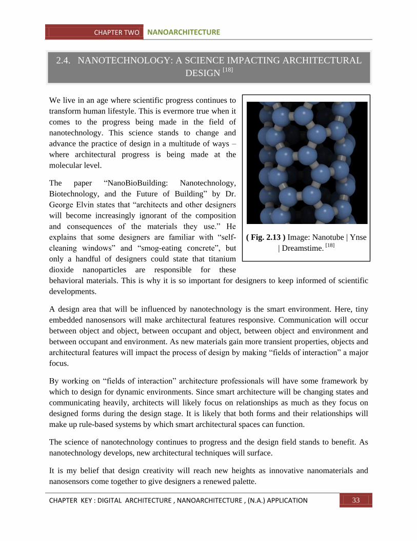
CHAPTER TWO NANOARCHITECTURE
CHAPTER KEY : DIGITAL ARCHITECTURE , NANOARCHITECTURE , (N.A.) APPLICATION 33
We live in an age where scientific progress continues to
transform human lifestyle. This is evermore true when it
comes to the progress being made in the field of
nanotechnology. This science stands to change and
advance the practice of design in a multitude of ways –
where architectural progress is being made at the
molecular level.
The paper “NanoBioBuilding: Nanotechnology,
Biotechnology, and the Future of Building” by Dr.
George Elvin states that “architects and other designers
will become increasingly ignorant of the composition
and consequences of the materials they use.” He
explains that some designers are familiar with “self-
cleaning windows” and “smog-eating concrete”, but
only a handful of designers could state that titanium
dioxide nanoparticles are responsible for these
behavioral materials. This is why it is so important for designers to keep informed of scientific
developments.
A design area that will be influenced by nanotechnology is the smart environment. Here, tiny
embedded nanosensors will make architectural features responsive. Communication will occur
between object and object, between occupant and object, between object and environment and
between occupant and environment. As new materials gain more transient properties, objects and
architectural features will impact the process of design by making “fields of interaction” a major
focus.
By working on “fields of interaction” architecture professionals will have some framework by
which to design for dynamic environments. Since smart architecture will be changing states and
communicating heavily, architects will likely focus on relationships as much as they focus on
designed forms during the design stage. It is likely that both forms and their relationships will
make up rule-based systems by which smart architectural spaces can function.
The science of nanotechnology continues to progress and the design field stands to benefit. As
nanotechnology develops, new architectural techniques will surface.
It is my belief that design creativity will reach new heights as innovative nanomaterials and
nanosensors come together to give designers a renewed palette.
2.4. NANOTECHNOLOGY: A SCIENCE IMPACTING ARCHITECTURAL
DESIGN [18]
( Fig. 2.13 ) Image: Nanotube | Ynse
| Dreamstime. [18]
CHAPTER TWO NANOARCHITECTURE
CHAPTER KEY : DIGITAL ARCHITECTURE , NANOARCHITECTURE , (N.A.) APPLICATION 34
“Small Plans” addresses questions about nanotechnology and the built environment at three
levels. First, what role does nanotechnology play today in architecture? Many nano-engineered
materials are already available to architects and builders, and are beginning to transform our
buildings, what we can do in them, and what they can do for us. Looking further ahead, new
nanotechnologies now in research and development will likely have a huge impact on building
within the next twenty to fifty years.
Carbon nanotubes, for example, could bring unprecedented strength and flexibility to our
buildings, leading to new forms, new functions, and new relationship between people, building
and environment. On the far horizon, the full impact of nanotechnology on our lives and our
environment into the next century and beyond is almost unimaginable. Theromprotectant skins,
invisible walls and self-replicating structures are all well within the realm of possibility; the
social, ethical and environmental effects are equally unimaginable and yet real.
Perhaps this is the promise and the peril of nanotechnology , that its consequences are so extreme
and yet so near, as billions of dollars pour into new research and development every year and
new advances pour out.
The real danger in nanotechnology is not rampant self-replicating viruses or nanobots
overunning the planet; the real danger is that, as most of us experienced wit cloning, we will
awake one day to find that a technological revolution has already occurred, without our
knowledge or our consent, and without us even taking time to determine what we think about it,
how we feel about it, or to share those thoughts and feelings in the discourse critical to a
reasoned advance in technology.
That day is coming sooner than we think. With its dawn will come new challenges and new
relationships between people, buildings and environment. Today is the day to reflect and to
discuss what those new challenges and relationships could be.
Winston Churchill was not thinking about nanotechnology when he said we shape our buildings
and our buildings shape us, but its power to transform us and our buildings brings new urgency
to the shaping.
Nanotechnology gives unprecedented power to the architects and engineers shaping our world,
and the result could be buildings that shape us, as well as our relationships with each other and
our environment, in ways that Churchill never could have envisioned.
2.5. NANOTECHNOLOGY, ARCHITECTURE AND FUTURE OF THE
BUILT ENVIRONMENT [33]
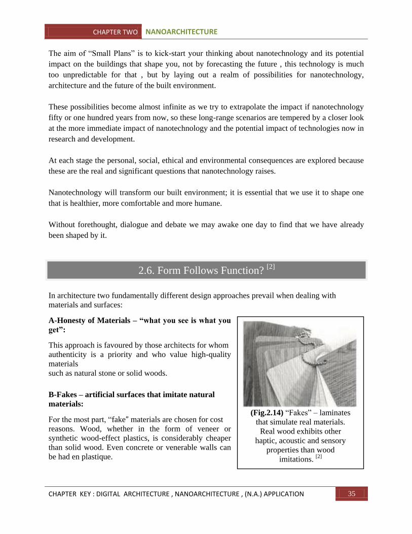
CHAPTER TWO NANOARCHITECTURE
CHAPTER KEY : DIGITAL ARCHITECTURE , NANOARCHITECTURE , (N.A.) APPLICATION 35
The aim of “Small Plans” is to kick-start your thinking about nanotechnology and its potential
impact on the buildings that shape you, not by forecasting the future , this technology is much
too unpredictable for that , but by laying out a realm of possibilities for nanotechnology,
architecture and the future of the built environment.
These possibilities become almost infinite as we try to extrapolate the impact if nanotechnology
fifty or one hundred years from now, so these long-range scenarios are tempered by a closer look
at the more immediate impact of nanotechnology and the potential impact of technologies now in
research and development.
At each stage the personal, social, ethical and environmental consequences are explored because
these are the real and significant questions that nanotechnology raises.
Nanotechnology will transform our built environment; it is essential that we use it to shape one
that is healthier, more comfortable and more humane.
Without forethought, dialogue and debate we may awake one day to find that we have already
been shaped by it.
In architecture two fundamentally different design approaches prevail when dealing with
materials and surfaces:
A-Honesty of Materials – “what you see is what you
get”:
This approach is favoured by those architects for whom
authenticity is a priority and who value high-quality
materials
such as natural stone or solid woods.
B-Fakes – artificial surfaces that imitate natural
materials:
For the most part, “fake” materials are chosen for cost
reasons. Wood, whether in the form of veneer or
synthetic wood-effect plastics, is considerably cheaper
than solid wood. Even concrete or venerable walls can
be had en plastique.
2.6. Form Follows Function? [2]
(Fig.2.14) “Fakes” – laminates
that simulate real materials.
Real wood exhibits other
haptic, acoustic and sensory
properties than wood
imitations. [2]
CHAPTER TWO NANOARCHITECTURE
CHAPTER KEY : DIGITAL ARCHITECTURE , NANOARCHITECTURE , (N.A.) APPLICATION 36
Artificial surfaces are “brought to perfection” – the grain can be tailored to appear exactly as
desired, the color matches the sample precisely and does not change over the course of time.
More and more “patinated” surfaces are being created that exhibit artificial aging: instant patinas
precisely controllable. Certain design approaches prefer the provocation of deliberate
artificiality. In future, a third option will be available:
C-Functional nanosurfaces, emancipated from underlying materials:
The properties of such ultra-thin surfaces can differ entirely from the material they enclose and
can be transparent and completely invisible. Also possible are nanocomposites with new
properties: nano particles or other nanomaterials are integrated into conventional materials so
that the characteristics of the original material are not only improved but can be accorded new
functional properties or even be made multifunctional. Surface materials that are customized to
have specific functional properties are set to become the norm, heralding a switch from catalogue
materials to made-to-measure materials with definable combination of properties – a perfectly
modular system.
Nanomaterials can extend our design possibilities. The aging process becomes a question of time
frame – it can set in earlier or later according to the material chosen. Likewise, aesthetic,
functional and emotional qualities can be expressed more easily – it is simply a matter of choice.
As such, "Form Follows Function” applies more than ever and for all kinds of building tasks.
Nanotechnology, the ability to manipulate matter at the scale of less than one billionth of a
meter, has the potential to transform the built environment in ways almost unimaginable today.
Nanotechnology is already employed in the manufacture of everyday items from sunscreen to
clothing, and its introduction to architecture is not far behind.
On the near horizon, it may take building enclosure materials (coatings, panels and insulation) to
dramatic new levels of performance in terms of energy, light, security and intelligence.
Even these first steps into the world of nanotechnology could dramatically alter the nature of
building enclosure and the way our buildings relate to environment and user.
At mid-horizon, the development of carbon nanotubes and other breakthrough materials could
radically alter building design and performance.
The entire distinction between structure and skin, for example, could disappear as ultralight,
super-strong materials functioning as both structural skeleton and enclosing skin are developed.
2.7. NANO ARCHITECTURE APPLICATION [34]
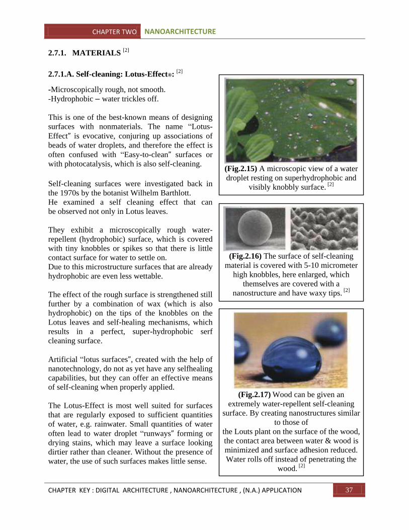
CHAPTER TWO NANOARCHITECTURE
CHAPTER KEY : DIGITAL ARCHITECTURE , NANOARCHITECTURE , (N.A.) APPLICATION 37
2.7.1. MATERIALS [2]
2.7.1.A. Self-cleaning: Lotus-Effect®: [2]
-Microscopically rough, not smooth.
-Hydrophobic – water trickles off.
This is one of the best-known means of designing
surfaces with nonmaterials. The name “Lotus-
Effect” is evocative, conjuring up associations of
beads of water droplets, and therefore the effect is
often confused with “Easy-to-clean” surfaces or
with photocatalysis, which is also self-cleaning.
Self-cleaning surfaces were investigated back in
the 1970s by the botanist Wilhelm Barthlott.
He examined a self cleaning effect that can
be observed not only in Lotus leaves.
They exhibit a microscopically rough water-
repellent (hydrophobic) surface, which is covered
with tiny knobbles or spikes so that there is little
contact surface for water to settle on.
Due to this microstructure surfaces that are already
hydrophobic are even less wettable.
The effect of the rough surface is strengthened still
further by a combination of wax (which is also
hydrophobic) on the tips of the knobbles on the
Lotus leaves and self-healing mechanisms, which
results in a perfect, super-hydrophobic serf
cleaning surface.
Artificial “lotus surfaces”, created with the help of
nanotechnology, do not as yet have any selfhealing
capabilities, but they can offer an effective means
of self-cleaning when properly applied.
The Lotus-Effect is most well suited for surfaces
that are regularly exposed to sufficient quantities
of water, e.g. rainwater. Small quantities of water
often lead to water droplet “runways” forming or
drying stains, which may leave a surface looking
dirtier rather than cleaner. Without the presence of
water, the use of such surfaces makes little sense.
(Fig.2.15) A microscopic view of a water
droplet resting on superhydrophobic and
visibly knobbly surface. [2]
(Fig.2.16) The surface of self-cleaning
material is covered with 5-10 micrometer
high knobbles, here enlarged, which
themselves are covered with a
nanostructure and have waxy tips. [2]
(Fig.2.17) Wood can be given an
extremely water-repellent self-cleaning
surface. By creating nanostructures similar
to those of
the Louts plant on the surface of the wood,
the contact area between water & wood is
minimized and surface adhesion reduced.
Water rolls off instead of penetrating the
wood. [2]

CHAPTER TWO NANOARCHITECTURE
CHAPTER KEY : DIGITAL ARCHITECTURE , NANOARCHITECTURE , (N.A.) APPLICATION 38
In all areas not subject to mechanical wear and
tear, the Lotus- Effect drastically reduces the
cleaning requirement and surfaces that are
regularly exposed to water remain clean.
The advantages are self-evident: a cleaner
appearance and considerably reduced maintenance
demands.
In the following pages is an example for the use of
the self-cleaning Lotus Effect applied on a
building surface for a better optimal use and low
maintenance façades:
Ara Pacis Museum, Rome, Italy:
Architecture Richard Meier & Partners, NYC, USA
Product Lotusan, self-cleaning paint (Lotus-Effect)
Manufacturer Sto
Opened 2006
After ten years of construction and political
debate, the Pacis Museum is now home to an
archaeological highlight in Rome.
A tripartite building complex consists of an
entrance gallery with an urban square in front, the
main building with the exhibits, conference rooms
and restaurant as well as further areas with space
for temporary exhibitions, library and offices.
The monument itself, the “Pax Augusta”, is now
contained within a transparent glazed part of the
building and protected against damage from the
environment.
The remainder of the building is characterized by
large blocks of travertine, typical for Rome, and
surfaces clad in white as typical Meier„s
architecture.
Here self-cleaning coating has been invisibly
integrated into the white surfaces to ensure the
durability of their color. In the heavily polluted
city, it would not otherwise have stood much
chance of remaining white for long.
(Fig.2.18) The diagram shows clearly the
difference between conventional surfaces
and the Lotus-Effect. [2]
(Fig.2.19.A) Ara Pacis Museum
exterior. [2]
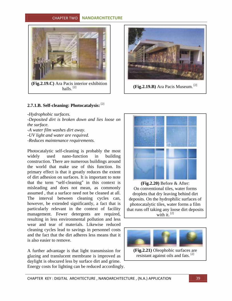
CHAPTER TWO NANOARCHITECTURE
CHAPTER KEY : DIGITAL ARCHITECTURE , NANOARCHITECTURE , (N.A.) APPLICATION 39
2.7.1.B. Self-cleaning: Photocatalysis: [2]
-Hydrophobic surfaces.
-Deposited dirt is broken down and lies loose on
the surface.
-A water film washes dirt away.
-UV light and water are required.
-Reduces maintenance requirements.
Photocatalytic self-cleaning is probably the most
widely used nano-function in building
construction. There are numerous buildings around
the world that make use of this function. Its
primary effect is that it greatly reduces the extent
of dirt adhesion on surfaces. It is important to note
that the term “self-cleaning” in this context is
misleading and does not mean, as commonly
assumed , that a surface need not be cleaned at all.
The interval between cleaning cycles can,
however, be extended significantly, a fact that is
particularly relevant in the context of facility
management. Fewer detergents are required,
resulting in less environmental pollution and less
wear and tear of materials. Likewise reduced
cleaning cycles lead to savings in personnel costs
and the fact that the dirt adheres less means that it
is also easier to remove.
A further advantage is that light transmission for
glazing and translucent membrane is improved as
daylight is obscured less by surface dirt and grime.
Energy costs for lighting can be reduced accordingly.
(Fig.2.19.B) Ara Pacis Museum. [2]
(Fig.2.19.C) Ara Pacis interior exhibition
halls. [2]
(Fig.2.20) Before & After:
On conventional tiles, water forms
droplets that dry leaving behind dirt
deposits. On the hydrophilic surfaces of
photocatalytic tiles, water forms a film
that runs off taking any loose dirt deposits
with it. [2]
(Fig.2.21) Oleophobic surfaces are
resistant against oils and fats. [2]
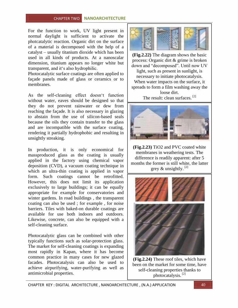
CHAPTER TWO NANOARCHITECTURE
CHAPTER KEY : DIGITAL ARCHITECTURE , NANOARCHITECTURE , (N.A.) APPLICATION 40
For the function to work, UV light present in
normal daylight is sufficient to activate the
photcatalytic reaction. Organic dirt on the surface
of a material is decomposed with the help of a
catalyst – usually titanium dioxide which has been
used in all kinds of products. At a nanoscalar
dimension, titanium appears no longer white but
transparent, and it„s also hydrophilic.
Photocatalytic surface coatings are often applied to
façade panels made of glass or ceramics or to
membranes.
As the self-cleaning effect doesn„t function
without water, eaves should be designed so that
they do not prevent rainwater or dew from
reaching the façade. It is also necessary in glazing
to abstain from the use of silicon-based seals
because the oils they contain transfer to the glass
and are incompatible with the surface coating,
rendering it partially hydrophobic and resulting in
unsightly streaking.
In production, it is only economical for
massproduced glass as the coating is usually
applied in the factory using chemical vapor
deposition (CVD), a vacuum coating technique in
which an ultra-thin coating is applied in vapor
form. Such coatings cannot be retrofitted.
However, this does not limit its application
exclusively to large buildings; it can be equally
appropriate for example for conservatories and
winter gardens. In road buildings , the transparent
coating can also be used ; for example , for noise
barriers. Tiles with baked-on durable coatings are
available for use both indoors and outdoors.
Likewise, concrete, can also be equipped with a
self-cleaning surface.
Photocatalytic glass can be combined with other
typically functions such as solar-protection glass.
The market for self-cleaning coatings is expanding
most rapidly in Kapan, where it has become
common practice in many cases for new glazed
facades. Photocatalysis can also be used to
achieve airpurifying, water-purifying as well as
antimicrobial properties.
(Fig.2.22) The diagram shows the basic
process: Organic dirt & grime is broken
down and “decomposed”. Until now UV
light, such as present in sunlight, is
necessary to initiate photocatalysis.
When water impacts on the surface, it
spreads to form a film washing away the
loose dirt.
The result: clean surfaces. [2]
(Fig.2.23) TiO2 and PVC coated white
membranes in weathering tests. The
difference is readily apparent: after 5
months the former is still white, the latter
grey & unsightly. [2]
(Fig.2.24) These roof tiles, which have
been on the market for some time, have
self-cleaning properties thanks to
photocatalysis. [2]

CHAPTER TWO NANOARCHITECTURE
CHAPTER KEY : DIGITAL ARCHITECTURE , NANOARCHITECTURE , (N.A.) APPLICATION 41
An interesting application is the exploitation of the cooling effect of evaporating water. The
canvas and steel roofing as well as the windows of a trade fair pavilion in Japan (Expo 2005)
were equipped with a photocatalytic TiO2 coating and subjected to a constant stream of water.
Duo to the hydrophilic property of the surface, the water immediately formed a thin film, which
evaporates quickly absorbing in the process ambient warmth and thereby reducing the indoor
temperature. Initial estimates suggest a potential energy reduction of between 10-20% in
comparison to conventional air conditioning.
Narita International Airport of Tokyo, Terminal 1, Chiba, Japan:
Architecture Nikken Sekkei Ltd., Japan
Product Ever Fine Coat/TiO2 photocatalytic self-cleaning membrane
Manufacturer Taiyo Kogyo Corporation
Opened 2006
Area 6.250m2
In 2006, The Narita International Airport
underwent comprehensive renovation. In the
process large were covered with textile.
Membranes offer protection against the weather
and therefore improving comfort for the
passengers.
As the membranes are equipped with a
photocatalytic self-cleaning coating, the cost of
cleaning and maintenance is kept to a minimum.
In central areas of Tokyo, the use of selfcleaning
awnings has been common practice for several
years and they have proven to remain much
cleaner than their conventional counterparts.
Although conventional surface coating, glass,
PTFE or ETFE materials are also self-cleaning,
they are not able to stop dirt deposits from
accumulating.
(Fig.2.25) Narita International Airport.
[2]
CHAPTER TWO NANOARCHITECTURE
CHAPTER KEY : DIGITAL ARCHITECTURE , NANOARCHITECTURE , (N.A.) APPLICATION 42
MSV Arena Soccer Stadium, Duisburg, Germany:
Architecture ar.te.plan, Burkhard Grimm, Michael Stehle, Dortmund, Germany
Product Pilkington Activ, photocatalytic self-cleaning glass
Manufacturer Pilkington Deutschland AG/Pilkington Group
Opened 2004
Area 18.0000m2 traffic area
A new soccer stadium was built in the centre of the Ruhr conurbation to house 30.000 fans of the
MSV, the Duisburg soccer club. More than 15.000m3 of concrete were used, 3500 tons of steel
reinforcement, around 30 steel pylons and last but not least 7.500m2 of turf (heated from beneath)
were laid and an almost 40m2 large screen was erected.
1.500m2 of glass were needed for the impressive 120m wide glass and aluminum façade. By
using a photocatalytic self-cleaning glass, the cleaning interval could be lengthened
considerably. In addition to its self-cleaning function, the glass wall also offers solar protection
and noise insulating properties.
2.7.1.C. Easy-to-clean (ETC): [2]
-Smooth surfaces with reduced surface attraction.
-Surface repellence without using the Lotus-Effect.
So-called easy-to-clean (ETC) surfaces are
waterrepellent and accordingly are often confused
with other self-cleaning functions such as the Lotus
Effect. However, unlike the latter, easy-to-clean
surfaces are smooth rather than rough. These
surfaces have a lower force of surface attraction due
to a decrease in their surface energy, resulting in
reduced surface adhesion. This causes water to be
repelled, forming droplets and running off. Easy-to
clean surfaces are therefore hydrophobic, and often
also oleophobic.
(Fig.2.26) MSV Arena Soccer Stadium. [2]
(Fig.2.27) “Roll-out marble” –
impactresistant, fire-resistant, vapour
permeable and yet water-repellent &
easy-to-clean. The product consists of 4
layers:
1-flexible polymer matting as backing
2-colored ceramic material is applied
3-optional printing
4-ceramised top coat [2]
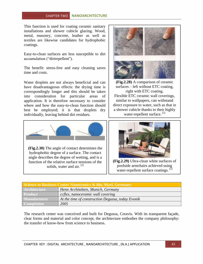
CHAPTER TWO NANOARCHITECTURE
CHAPTER KEY : DIGITAL ARCHITECTURE , NANOARCHITECTURE , (N.A.) APPLICATION 43
This function is used for coating ceramic sanitary
installations and shower cubicle glazing. Wood,
metal, masonry, concrete, leather as well as
textiles are likewise candidates for hydrophobic
coatings.
Easy-to-clean surfaces are less susceptible to dirt
accumulation (“dirtrepellent”).
The benefit: stress-free and easy cleaning saves
time and costs.
Water droplets are not always beneficial and can
have disadvantageous effects: the drying time is
correspondingly longer and this should be taken
into consideration for particular areas of
application. It is therefore necessary to consider
where and how the easy-to-clean function should
best be employed; it is that droplets dry
individually, leaving behind dirt residues.
Science to Business Center Nanotronics & Bio, Marl, Germany:
Architecture Henn Architekten, Munich, Germany
Product ccflex, nanoceramic wall covering
Manufacturer At the time of construction Degussa, today Evonik
Completion 2005
The research center was conceived and built for Degussa, Creavis. With its transparent façade,
clear forms and material and color concept, the architecture embodies the company philosophy:
the transfer of know-how from science to business.
(Fig.2.28) A comparison of ceramic
surfaces – left without ETC coating,
right with ETC coating.
Flexible ETC ceramic wall coverings,
similar to wallpapers, can withstand
direct exposure to water, such as that in
a shower cubicle thanks to their highly
water-repellent surface. [2]
(Fig.2.29) Ultra-clean white surfaces of
poolside armchairs achieved using
water-repellent surface coatings. [2]
(Fig.2.30) The angle of contact determines the
hydrophobic degree of a surface. The contact
angle describes the degree of wetting, and is a
function of the relative surface tensions of the
solids, water and air. [2]
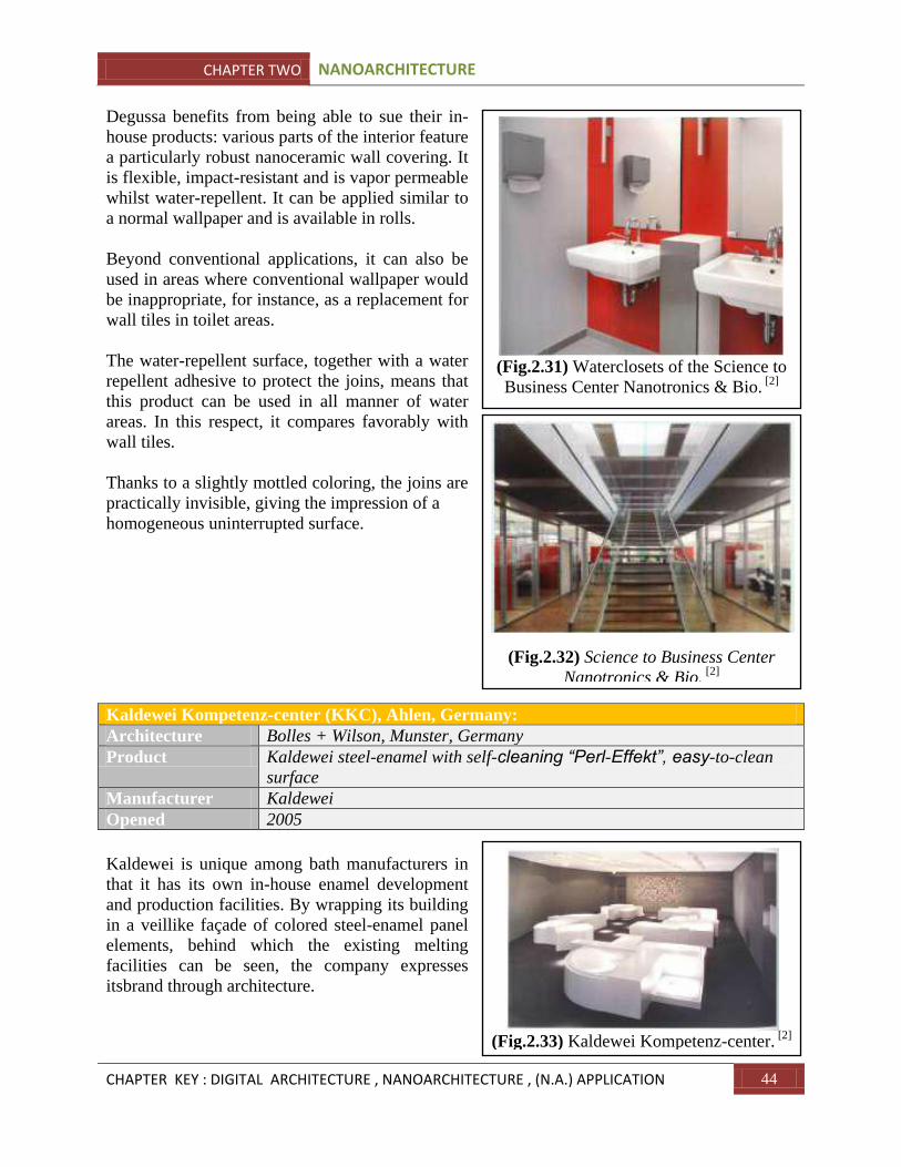
CHAPTER TWO NANOARCHITECTURE
CHAPTER KEY : DIGITAL ARCHITECTURE , NANOARCHITECTURE , (N.A.) APPLICATION 44
Degussa benefits from being able to sue their in-
house products: various parts of the interior feature
a particularly robust nanoceramic wall covering. It
is flexible, impact-resistant and is vapor permeable
whilst water-repellent. It can be applied similar to
a normal wallpaper and is available in rolls.
Beyond conventional applications, it can also be
used in areas where conventional wallpaper would
be inappropriate, for instance, as a replacement for
wall tiles in toilet areas.
The water-repellent surface, together with a water
repellent adhesive to protect the joins, means that
this product can be used in all manner of water
areas. In this respect, it compares favorably with
wall tiles.
Thanks to a slightly mottled coloring, the joins are
practically invisible, giving the impression of a
homogeneous uninterrupted surface.
Kaldewei Kompetenz-center (KKC), Ahlen, Germany:
Architecture Bolles + Wilson, Munster, Germany
Product Kaldewei steel-enamel with self-cleaning “Perl-Effekt”, easy-to-clean
surface
Manufacturer Kaldewei
Opened 2005
Kaldewei is unique among bath manufacturers in
that it has its own in-house enamel development
and production facilities. By wrapping its building
in a veillike façade of colored steel-enamel panel
elements, behind which the existing melting
facilities can be seen, the company expresses
itsbrand through architecture.
(Fig.2.31) Waterclosets of the Science to
Business Center Nanotronics & Bio. [2]
(Fig.2.32) Science to Business Center
Nanotronics & Bio. [2]
(Fig.2.33) Kaldewei Kompetenz-center. [2]
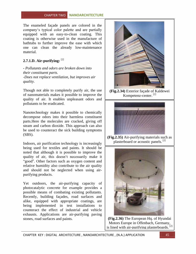
CHAPTER TWO NANOARCHITECTURE
CHAPTER KEY : DIGITAL ARCHITECTURE , NANOARCHITECTURE , (N.A.) APPLICATION 45
The enameled façade panels are colored in the
company„s typical color palette and are partially
equipped with an easy-to-clean coating. This
coating is otherwise used in the manufacture of
bathtubs to further improve the ease with which
one can clean the already low-maintenance
material.
2.7.1.D. Air-purifying: [2]
- Pollutants and odors are broken down into
their constituent parts.
-Does not replace ventilation, but improves air
quality.
Though not able to completely purify air, the use
of nanomaterials makes it possible to improve the
quality of air. It enables unpleasant odors and
pollutants to be eradicated.
Nanotechnology makes it possible to chemically
decompose odors into their harmless constituent
parts.Here the molecules are cracked, giving off
steam and carbon dioxide. This approach can also
be used to counteract the sick building symptoms
(SBS).
Indoors, air purification technology is increasingly
being used for textiles and paints. It should be
noted that although it is possible to improve the
quality of air, this doesn„t necessarily make it
“good”. Other factors such as oxygen content and
relative humidity also contribute to the air quality
and should not be neglected when using air-
purifying products.
Yet outdoors, the air-purifying capacity of
photocatalytic concrete for example provides a
possible means of combating existing pollutants.
Recently, building façades, road surfaces and
alike, equipped with appropriate coatings, are
being implemented in test installations to
counteract the effect of industrial and vehicle
exhausts. Applications are air-purifying paving
stones, road surfaces and paints.
(Fig.2.34) Exterior façade of Kaldewei
Kompetenz-center. [2]
(Fig.2.35) Air-purifying materials such as
plasterboard or acoustic panels. [2]
(Fig.2.36) The European Hq. of Hyundai
Motors Europe in Offenbach, Germany,
is lined with air-purifying plasterboards. [2]
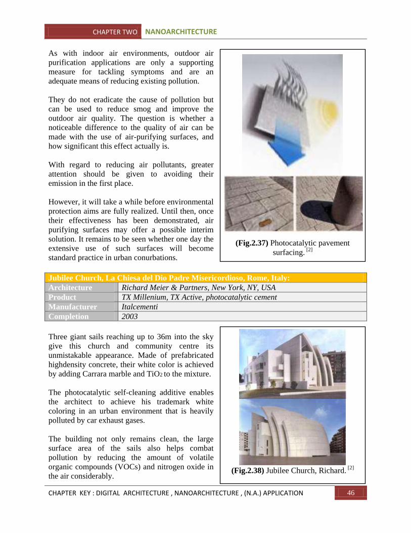
CHAPTER TWO NANOARCHITECTURE
CHAPTER KEY : DIGITAL ARCHITECTURE , NANOARCHITECTURE , (N.A.) APPLICATION 46
As with indoor air environments, outdoor air
purification applications are only a supporting
measure for tackling symptoms and are an
adequate means of reducing existing pollution.
They do not eradicate the cause of pollution but
can be used to reduce smog and improve the
outdoor air quality. The question is whether a
noticeable difference to the quality of air can be
made with the use of air-purifying surfaces, and
how significant this effect actually is.
With regard to reducing air pollutants, greater
attention should be given to avoiding their
emission in the first place.
However, it will take a while before environmental
protection aims are fully realized. Until then, once
their effectiveness has been demonstrated, air
purifying surfaces may offer a possible interim
solution. It remains to be seen whether one day the
extensive use of such surfaces will become
standard practice in urban conurbations.
Jubilee Church, La Chiesa del Dio Padre Misericordioso, Rome, Italy:
Architecture Richard Meier & Partners, New York, NY, USA
Product TX Millenium, TX Active, photocatalytic cement
Manufacturer Italcementi
Completion 2003
Three giant sails reaching up to 36m into the sky
give this church and community centre its
unmistakable appearance. Made of prefabricated
highdensity concrete, their white color is achieved
by adding Carrara marble and TiO2 to the mixture.
The photocatalytic self-cleaning additive enables
the architect to achieve his trademark white
coloring in an urban environment that is heavily
polluted by car exhaust gases.
The building not only remains clean, the large
surface area of the sails also helps combat
pollution by reducing the amount of volatile
organic compounds (VOCs) and nitrogen oxide in
the air considerably.
(Fig.2.37) Photocatalytic pavement
surfacing. [2]
(Fig.2.38) Jubilee Church, Richard. [2]
Meier.
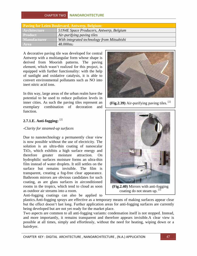
CHAPTER TWO NANOARCHITECTURE
CHAPTER KEY : DIGITAL ARCHITECTURE , NANOARCHITECTURE , (N.A.) APPLICATION 47
Paving for Leien Boulevard, Antwerp, Belgium:
Architecture 51N4E Space Producers, Antwerp, Belgium
Product Air-purifying paving tiles
Manufacturer With integrated technology from Mitsubishi
Area 48.000m2
A decorative paving tile was developed for central
Antwerp with a multiangular form whose shape is
derived from Moorish patterns. The paving
element, which wasn„t realized for this project, is
equipped with further functionality: with the help
of sunlight and oxidative catalysis, it is able to
convert environmental pollutants such as NO into
inert nitric acid ions.
In this way, large areas of the urban realm have the
potential to be used to reduce pollution levels in
inner cities. As such the paving tiles represent an
exemplary combination of decoration and
function.
2.7.1.E. Anti-fogging: [2]
-Clarity for steamed-up surfaces
Due to nanotechnology a permanently clear view
is now possible without the use of electricity. The
solution is an ultra-thin coating of nanoscalar
TiO2, which exhibits a high surface energy and
therefore greater moisture attraction. On
hydrophilic surfaces moisture forms an ultra-thin
film instead of water droplets. It still settles on the
surface but remains invisible. The film is
transparent, creating a fog-free clear appearance.
Bathroom mirrors are obvious candidates for such
coating, as are glass surfaces in airconditioned
rooms in the tropics, which tend to cloud as soon
as outdoor air streams into a room.
Anti-fogging coatings can also be applied to
plastics.Anti-fogging sprays are effective as a temporary means of making surfaces appear clear
but the effect doesn„t last long. Further application areas for anti-fogging surfaces are currently
being developed but are not yet ready for the market place.
Two aspects are common to all anti-fogging variants: condensation itself is not stopped. Instead,
and more importantly, it remains transparent and therefore appears invisible.A clear view is
possible at all times, simply and effortlessly, without the need for heating, wiping down or a
hairdryer.
(Fig.2.39) Air-purifying paving tiles. [2]
(Fig.2.40) Mirrors with anti-fogging
coating do not steam up. [2]
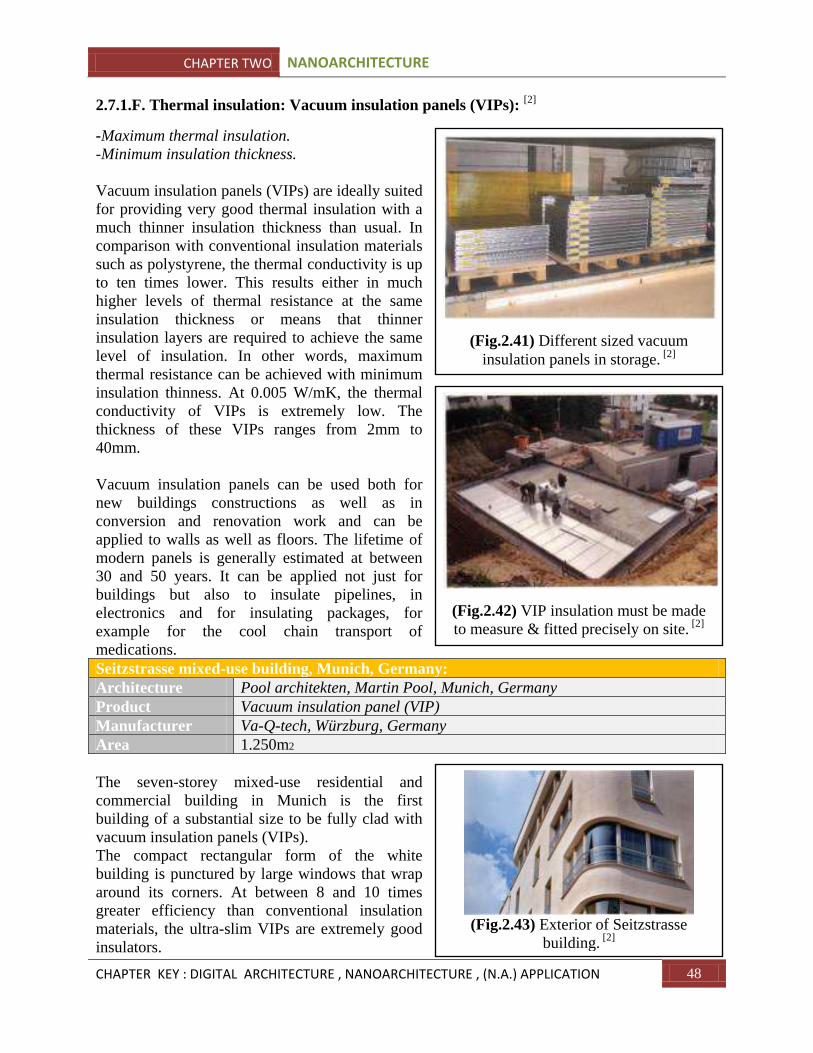
CHAPTER TWO NANOARCHITECTURE
CHAPTER KEY : DIGITAL ARCHITECTURE , NANOARCHITECTURE , (N.A.) APPLICATION 48
2.7.1.F. Thermal insulation: Vacuum insulation panels (VIPs): [2]
-Maximum thermal insulation.
-Minimum insulation thickness.
Vacuum insulation panels (VIPs) are ideally suited
for providing very good thermal insulation with a
much thinner insulation thickness than usual. In
comparison with conventional insulation materials
such as polystyrene, the thermal conductivity is up
to ten times lower. This results either in much
higher levels of thermal resistance at the same
insulation thickness or means that thinner
insulation layers are required to achieve the same
level of insulation. In other words, maximum
thermal resistance can be achieved with minimum
insulation thinness. At 0.005 W/mK, the thermal
conductivity of VIPs is extremely low. The
thickness of these VIPs ranges from 2mm to
40mm.
Vacuum insulation panels can be used both for
new buildings constructions as well as in
conversion and renovation work and can be
applied to walls as well as floors. The lifetime of
modern panels is generally estimated at between
30 and 50 years. It can be applied not just for
buildings but also to insulate pipelines, in
electronics and for insulating packages, for
example for the cool chain transport of
medications.
Seitzstrasse mixed-use building, Munich, Germany:
Architecture Pool architekten, Martin Pool, Munich, Germany
Product Vacuum insulation panel (VIP)
Manufacturer Va-Q-tech, Würzburg, Germany
Area 1.250m2
The seven-storey mixed-use residential and
commercial building in Munich is the first
building of a substantial size to be fully clad with
vacuum insulation panels (VIPs).
The compact rectangular form of the white
building is punctured by large windows that wrap
around its corners. At between 8 and 10 times
greater efficiency than conventional insulation
materials, the ultra-slim VIPs are extremely good
insulators.
(Fig.2.41) Different sized vacuum
insulation panels in storage. [2]
(Fig.2.42) VIP insulation must be made
to measure & fitted precisely on site. [2]
(Fig.2.43) Exterior of Seitzstrasse
building. [2]

CHAPTER TWO NANOARCHITECTURE
CHAPTER KEY : DIGITAL ARCHITECTURE , NANOARCHITECTURE , (N.A.) APPLICATION 49
Their potential lies not only in reducing energy
consumption but also in maximizing the available
area as result of thinner wall constructions. It
resulted in a floor area gain of 10% of the overall
floor area.
VIPs were also used in the roof terrace and
window constructions. This inner-city building
leads to energy savings as well as increased
economic returns.
2.7.1.G. Thermal insulation: Aerogel: [2]
-High-performance thermal insulation.
-Light and airy nanofoam.
Aerogel currently holds the record as the lightest
known solid material and was developed back in
1931. It is relatively banal: it is simply an ultra
light aerated foam that consists almost 100% of
air. The remaining foam material is a glass-like
material, and silica.
The nanodimension is of vital importance for the
pore interstices of the foam: the air molecules
trapped within the minute nanpores –each with a
mean size of just 20nm – are unable to move,
lending the aerogel its excellent thermal insulation
properties.
It is used as an insulating fill material in various
kinds of cavities – between glass panes, U-profile
glass or acrylic glass multi-wall panels – and is
therefore well suited for use in external envelopes
of buildings. That way aerogels can help reduce
heating and cooling costs significantly. Because it
is translucent, aerogel exhibits good light
transmission, spreading light evenly and
pleasantly. In addition to its thermal insulating
properties, aerogel also acts as a sound insulator
according to the same basic principle.
With its above-average thermal and sound
insulation properties aerogel contributes towards
energy efficiency, which is its primary functional property. It is an extraordinary high
performance insulator and a comparatively new product on the market. A further advantage is its
good light transmission and daylight transmittance. From an aesthetic point of view, its light
weight makes homogeneous and slender façade constructions possible – all in all a whole
catalogue of advantages with great potential.
(Fig.2.44) Seitzstrasse building rooftop. [2]
(Fig.2.45) Aerogel in combination with
glass. [2]
(Fig.2.46) Glass sample with black
edging & aerogel-filled glazing cavity. [2]
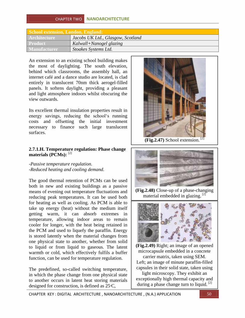
CHAPTER TWO NANOARCHITECTURE
CHAPTER KEY : DIGITAL ARCHITECTURE , NANOARCHITECTURE , (N.A.) APPLICATION 50
School extension, London, England:
Architecture Jacobs UK Ltd., Glasgow, Scotland
Product Kalwall+Nanogel glazing
Manufacturer Stoakes Systems Ltd.
An extension to an existing school building makes
the most of daylighting. The south elevation,
behind which classrooms, the assembly hall, an
internet café and a dance studio are located, is clad
entirely in translucent 70nm thick aerogel-filled
panels. It softens daylight, providing a pleasant
and light atmosphere indoors whilst obscuring the
view outwards.
Its excellent thermal insulation properties result in
energy savings, reducing the school„s running
costs and offsetting the initial investment
necessary to finance such large translucent
surfaces.
2.7.1.H. Temperature regulation: Phase change
materials (PCMs): [2]
-Passive temperature regulation.
-Reduced heating and cooling demand.
The good thermal retention of PCMs can be used
both in new and existing buildings as a passive
means of evening out temperature fluctuations and
reducing peak temperatures. It can be used both
for heating as well as cooling. As PCM is able to
take up energy (heat) without the medium itself
getting warm, it can absorb extremes in
temperature, allowing indoor areas to remain
cooler for longer, with the heat being retained in
the PCM and used to liquefy the paraffin. Energy
is stored latently when the material changes from
one physical state to another, whether from solid
to liquid or from liquid to gaseous. The latent
warmth or cold, which effectively fulfils a buffer
function, can be used for temperature regulation.
The predefined, so-called switching temperature,
in which the phase change from one physical state
to another occurs in latent heat storing materials
designed for construction, is defined as 25oC,
(Fig.2.47) School extension. [2]
(Fig.2.48) Close-up of a phase-changing
material embedded in glazing. [2]
(Fig.2.49) Right; an image of an opened
microcapsule embedded in a concrete
carrier matrix, taken using SEM.
Left; an image of minute paraffin-filled
capsules in their solid state, taken using
light microscopy. They exhibit an
exceptionally high thermal capacity and
during a phase change turn to liquid. [2]
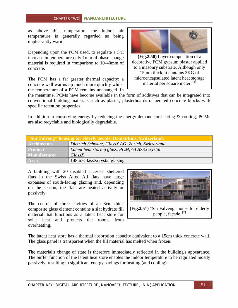
CHAPTER TWO NANOARCHITECTURE
CHAPTER KEY : DIGITAL ARCHITECTURE , NANOARCHITECTURE , (N.A.) APPLICATION 51
as above this temperature the indoor air
temperature is generally regarded as being
unpleasantly warm.
Depending upon the PCM used, to regulate a 5oC
increase in temperature only 1mm of phase change
material is required in comparison to 10-40mm of
concrete.
The PCM has a far greater thermal capacity: a
concrete wall warms up much more quickly whilst
the temperature of a PCM remains unchanged. In
the meantime, PCMs have become available in the form of additives that can be integrated into
conventional building materials such as plaster, plasterboards or aerated concrete blocks with
specific retention properties.
In addition to conserving energy by reducing the energy demand for heating & cooling, PCMs
are also recyclable and biologically degradable.
"Sur Falveng" housing for elderly people, Domat/Ems, Switzerland:
Architecture Dietrich Schwarz, GlassX AG, Zurich, Switzerland
Product Latent heat storing glass, PCM, GLASSXcrystal
Manufacturer GlassX
Area 148m2 GlassXcrystal glazing
A building with 20 disabled accesses sheltered
flats in the Swiss Alps. All flats have large
expanses of south-facing glazing and, depending
on the season, the flats are heated actively or
passively.
The central of three cavities of an 8cm thick
composite glass element contains a slat hydrate fill
material that functions as a latent heat store for
solar heat and protects the rooms from
overheating.
The latent heat store has a thermal absorption capacity equivalent to a 15cm thick concrete wall.
The glass panel is transparent when the fill material has melted when frozen.
The material's change of state is therefore immediately reflected in the building's appearance.
The buffer function of the latent heat store enables the indoor temperature to be regulated mostly
passively, resulting in significant energy savings for heating (and cooling).
(Fig.2.50) Layer composition of a
decorative PCM gypsum plaster applied
to a masonry substrate. Although only
15mm thick, it contains 3KG of
microencapsulated latent heat storage
material per square meter. [2]
(Fig.2.51) "Sur Falveng" house for elderly
people, façade. [2]
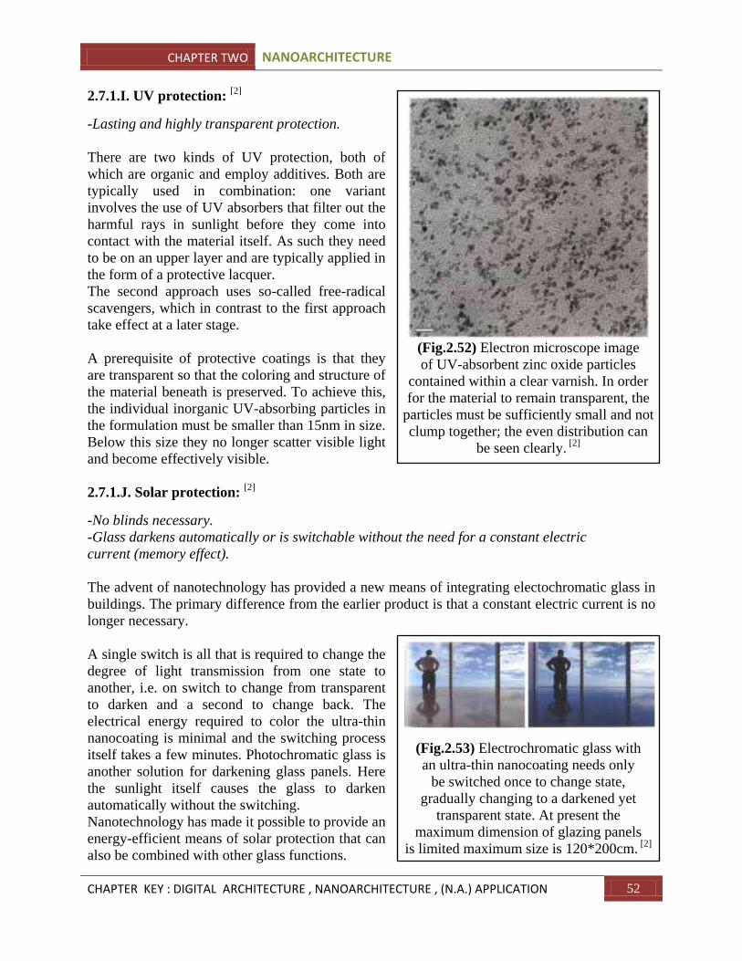
CHAPTER TWO NANOARCHITECTURE
CHAPTER KEY : DIGITAL ARCHITECTURE , NANOARCHITECTURE , (N.A.) APPLICATION 52
2.7.1.I. UV protection: [2]
-Lasting and highly transparent protection.
There are two kinds of UV protection, both of
which are organic and employ additives. Both are
typically used in combination: one variant
involves the use of UV absorbers that filter out the
harmful rays in sunlight before they come into
contact with the material itself. As such they need
to be on an upper layer and are typically applied in
the form of a protective lacquer.
The second approach uses so-called free-radical
scavengers, which in contrast to the first approach
take effect at a later stage.
A prerequisite of protective coatings is that they
are transparent so that the coloring and structure of
the material beneath is preserved. To achieve this,
the individual inorganic UV-absorbing particles in
the formulation must be smaller than 15nm in size.
Below this size they no longer scatter visible light
and become effectively visible.
2.7.1.J. Solar protection: [2]
-No blinds necessary.
-Glass darkens automatically or is switchable without the need for a constant electric
current (memory effect).
The advent of nanotechnology has provided a new means of integrating electochromatic glass in
buildings. The primary difference from the earlier product is that a constant electric current is no
longer necessary.
A single switch is all that is required to change the
degree of light transmission from one state to
another, i.e. on switch to change from transparent
to darken and a second to change back. The
electrical energy required to color the ultra-thin
nanocoating is minimal and the switching process
itself takes a few minutes. Photochromatic glass is
another solution for darkening glass panels. Here
the sunlight itself causes the glass to darken
automatically without the switching.
Nanotechnology has made it possible to provide an
energy-efficient means of solar protection that can
also be combined with other glass functions.
(Fig.2.52) Electron microscope image
of UV-absorbent zinc oxide particles
contained within a clear varnish. In order
for the material to remain transparent, the
particles must be sufficiently small and not
clump together; the even distribution can
be seen clearly. [2]
(Fig.2.53) Electrochromatic glass with
an ultra-thin nanocoating needs only
be switched once to change state,
gradually changing to a darkened yet
transparent state. At present the
maximum dimension of glazing panels
is limited maximum size is 120*200cm. [2]
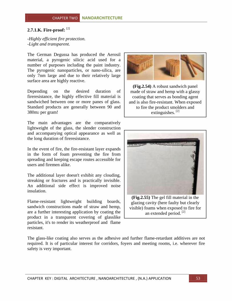
CHAPTER TWO NANOARCHITECTURE
CHAPTER KEY : DIGITAL ARCHITECTURE , NANOARCHITECTURE , (N.A.) APPLICATION 53
2.7.1.K. Fire-proof: [2]
-Highly efficient fire protection.
-Light and transparent.
The German Degussa has produced the Aerosil
material, a pyrogenic silicic acid used for a
number of purposes including the paint industry.
The pyrogenic nanoparticles, or nano-silica, are
only 7nm large and due to their relatively large
surface area are highly reactive.
Depending on the desired duration of
fireresistance, the highly effective fill material is
sandwiched between one or more panes of glass.
Standard products are generally between 90 and
380m2 per gram!
The main advantages are the comparatively
lightweight of the glass, the slender construction
and accompanying optical appearance as well as
the long duration of fireresistance.
In the event of fire, the fire-resistant layer expands
in the form of foam preventing the fire from
spreading and keeping escape routes accessible for
users and firemen alike.
The additional layer doesn't exhibit any clouding,
streaking or fractures and is practically invisible.
An additional side effect is improved noise
insulation.
Flame-resistant lightweight building boards,
sandwich constructions made of straw and hemp,
are a further interesting application by coating the
product in a transparent covering of glasslike
particles, it's to render its weatherproof and flame
resistant.
The glass-like coating also serves as the adhesive and further flame-retardant additives are not
required. It is of particular interest for corridors, foyers and meeting rooms, i.e. wherever fire
safety is very important.
(Fig.2.54) A robust sandwich panel
made of straw and hemp with a glassy
coating that serves as bonding agent
and is also fire-resistant. When exposed
to fire the product smolders and
extinguishes. [2]
(Fig.2.55) The gel fill material in the
glazing cavity (here faulty but clearly
visible) foams when exposed to fire for
an extended period. [2]
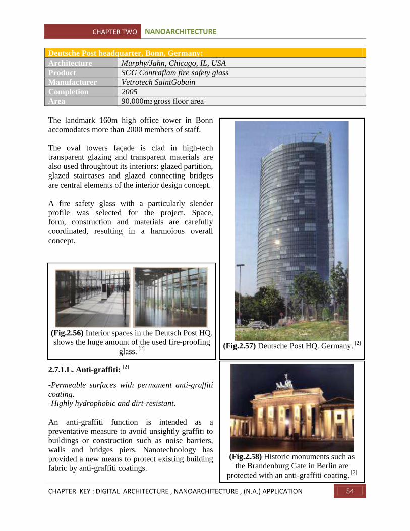
CHAPTER TWO NANOARCHITECTURE
CHAPTER KEY : DIGITAL ARCHITECTURE , NANOARCHITECTURE , (N.A.) APPLICATION 54
Deutsche Post headquarter, Bonn, Germany:
Architecture Murphy/Jahn, Chicago, IL, USA
Product SGG Contraflam fire safety glass
Manufacturer Vetrotech SaintGobain
Completion 2005
Area 90.000m2 gross floor area
The landmark 160m high office tower in Bonn
accomodates more than 2000 members of staff.
The oval towers façade is clad in high-tech
transparent glazing and transparent materials are
also used throughtout its interiors: glazed partition,
glazed staircases and glazed connecting bridges
are central elements of the interior design concept.
A fire safety glass with a particularly slender
profile was selected for the project. Space,
form, construction and materials are carefully
coordinated, resulting in a harmoious overall
concept.
2.7.1.L. Anti-graffiti: [2]
-Permeable surfaces with permanent anti-graffiti
coating.
-Highly hydrophobic and dirt-resistant.
An anti-graffiti function is intended as a
preventative measure to avoid unsightly graffiti to
buildings or construction such as noise barriers,
walls and bridges piers. Nanotechnology has
provided a new means to protect existing building
fabric by anti-graffiti coatings.
(Fig.2.57) Deutsche Post HQ. Germany. [2]
(Fig.2.56) Interior spaces in the Deutsch Post HQ.
shows the huge amount of the used fire-proofing
glass. [2]
(Fig.2.58) Historic monuments such as
the Brandenburg Gate in Berlin are
protected with an anti-graffiti coating. [2]
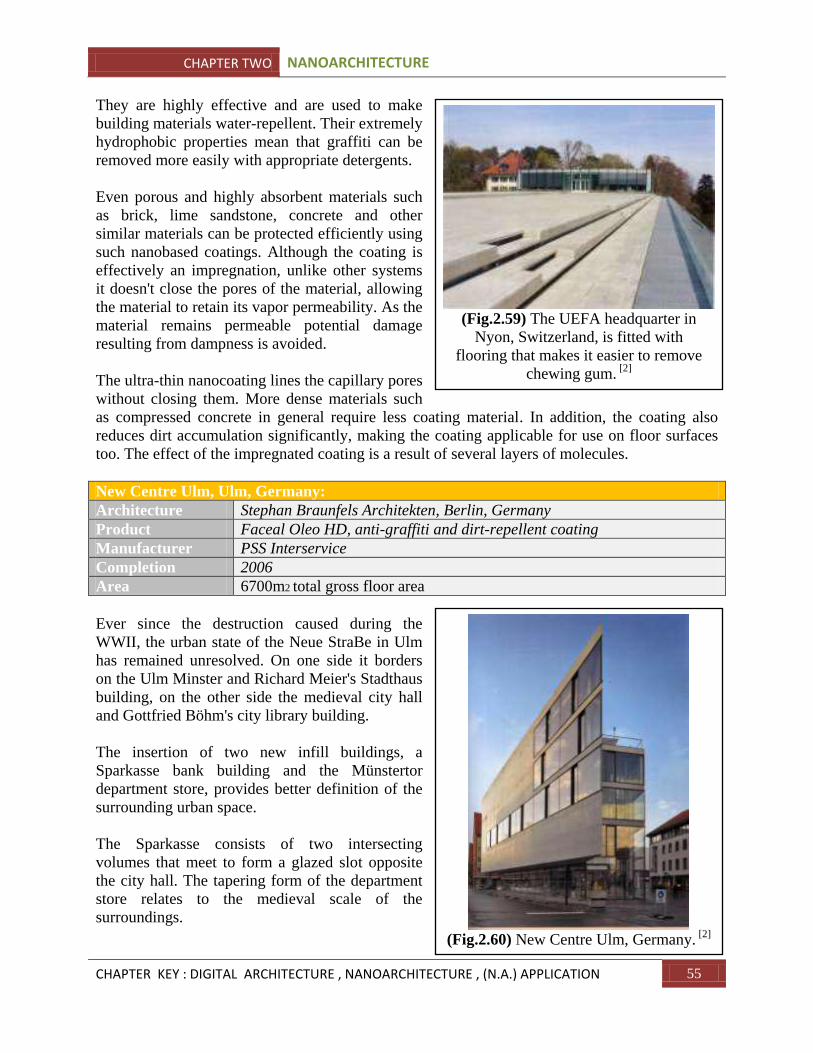
CHAPTER TWO NANOARCHITECTURE
CHAPTER KEY : DIGITAL ARCHITECTURE , NANOARCHITECTURE , (N.A.) APPLICATION 55
They are highly effective and are used to make
building materials water-repellent. Their extremely
hydrophobic properties mean that graffiti can be
removed more easily with appropriate detergents.
Even porous and highly absorbent materials such
as brick, lime sandstone, concrete and other
similar materials can be protected efficiently using
such nanobased coatings. Although the coating is
effectively an impregnation, unlike other systems
it doesn't close the pores of the material, allowing
the material to retain its vapor permeability. As the
material remains permeable potential damage
resulting from dampness is avoided.
The ultra-thin nanocoating lines the capillary pores
without closing them. More dense materials such
as compressed concrete in general require less coating material. In addition, the coating also
reduces dirt accumulation significantly, making the coating applicable for use on floor surfaces
too. The effect of the impregnated coating is a result of several layers of molecules.
New Centre Ulm, Ulm, Germany:
Architecture Stephan Braunfels Architekten, Berlin, Germany
Product Faceal Oleo HD, anti-graffiti and dirt-repellent coating
Manufacturer PSS Interservice
Completion 2006
Area 6700m2 total gross floor area
Ever since the destruction caused during the
WWII, the urban state of the Neue StraBe in Ulm
has remained unresolved. On one side it borders
on the Ulm Minster and Richard Meier's Stadthaus
building, on the other side the medieval city hall
and Gottfried Böhm's city library building.
The insertion of two new infill buildings, a
Sparkasse bank building and the Münstertor
department store, provides better definition of the
surrounding urban space.
The Sparkasse consists of two intersecting
volumes that meet to form a glazed slot opposite
the city hall. The tapering form of the department
store relates to the medieval scale of the
surroundings.
(Fig.2.59) The UEFA headquarter in
Nyon, Switzerland, is fitted with
flooring that makes it easier to remove
chewing gum. [2]
(Fig.2.60) New Centre Ulm, Germany. [2]
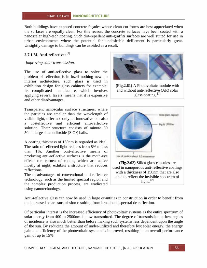
CHAPTER TWO NANOARCHITECTURE
CHAPTER KEY : DIGITAL ARCHITECTURE , NANOARCHITECTURE , (N.A.) APPLICATION 56
Both buildings have exposed concrete façades whose clean-cut forms are best appreciated when
the surfaces are equally clean. For this reason, the concrete surfaces have been coated with a
nanoscalar high-tech coating. Such dirt-repellent anti-graffiti surfaces are well suited for use in
urban environments where the potential for undesirable defilement is particularly great.
Unsightly damage to buildings can be avoided as a result.
2.7.1.M. Anti-reflective: [2]
-Improving solar transmission.
The use of anti-reflective glass to solve the
problem of reflection is in itself nothing new. In
interior architecture, such glass is used in
exhibition design for glass cabinets for example.
Its complicated manufacture, which involves
applying several layers, means that it is expensive
and other disadvantages.
Transparent nanoscalar surface structures, where
the particles are smaller than the wavelength of
visible light, offer not only an innovative but also
a costeffective and efficient anti-reflective
solution. Their structure consists of minute 30
50nm large silicondioxide (SiO2) balls.
A coating thickness of 150nm is regarded as ideal.
The ratio of reflected light reduces from 8% to less
than 1%. Another cost-effective means of
producing anti-reflective surfaces is the moth-eye
effect, the cornea of moths, which are active
mostly at night, exhibits a structure that reduces
reflections.
The disadvantages of conventional anti-reflective
technology, such as the limited spectral region and
the complex production process, are eradicated
using nanotechnology.
Anti-reflective glass can now be used in large quantities in construction in order to benefit from
the increased solar transmission resulting from broadband spectral de-reflection.
Of particular interest is the increased efficiency of photovoltaic systems as the entire spectrum of
solar energy from 400 to 2500nm is now transmitted. The degree of transmission at low angles
of incidence is also much better than before making such systems less dependent upon the angle
of the sun. By reducing the amount of under-utilized and therefore lost solar energy, the energy
gain and efficiency of the photovoltaic systems is improved, resulting in an overall performance
gain of up to 15%.
(Fig.2.61) A Photovoltaic module with
and without anti-reflective (AR) solar
glass coating. [2]
(Fig.2.62) Silica glass capsules are
used in nanoporous anti-reflective coatings
with a thickness of 150nm that are also
able to reflect the invisible spectrum of
light. [2]

CHAPTER TWO NANOARCHITECTURE
CHAPTER KEY : DIGITAL ARCHITECTURE , NANOARCHITECTURE , (N.A.) APPLICATION 57
2.7.1.N. Antibacterial: [2]
-Bactria are targeted and destroyed.
-The use of disinfectants can be reduced.
-Supports hygiene methods – especially in health care environments
Photocatalytic surfaces have an antibacterial side
effect due to their ability to break down organic
substances in dirt. With the help of silver
nanoparticles –for its antimicrobial properties, it is
possible to manufacture surfaces specifically
designed to be antibacterial or germicidal.
Various products are already commercially
available and the product palette ranges from floor
coverings to panel products and paints to textiles
with an innovative finish that renders them germ
free.
The antibacterial effect of silver results from the
ongoing slow diffusion of silver ions. The very
high surface area to volume ratio of the
nanoparticles means that the ions can be emitted
more easily and therefore kill bacteria more
effectively. The antibacterial effect itself is also
permanent – it doesn't wear off after a period of
time.
As the use of disinfectants in health care cannot
yet be avoided, it is important that coatings and
materials are proven to withstand standard
disinfections. In addition, it is also advisable to
equip surfaces with an anti-stick function to
prevent the buildup of a bio-film of dead bacteria
from which new bacteria could eventually grow.
Operating Theatre, Goslar, Germany:
Architecture Schweitzer + Partner, Braunschweig, Germany
Product "Hydrotect" tiles, photocatalytic surface with antibacterial effect
Manufacturer Agrob Buchtal Architectural Ceramic, Deutsche Steinzeug AG
Completion 2005
(Fig.2.63) Contact surfaces such as
light switches, door grips and handles
are typical germ accumulators. An
antibacterial material, such as that
used for this light switch, can prevent
germs spreading. [2]
(Fig.2.64) Nanoscalar silver particles
contained in the glaze applied to ceramic
sanitary installations lend it antibacterial
properties. [2]
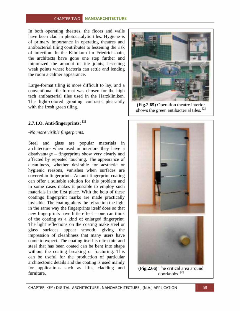
CHAPTER TWO NANOARCHITECTURE
CHAPTER KEY : DIGITAL ARCHITECTURE , NANOARCHITECTURE , (N.A.) APPLICATION 58
In both operating theatres, the floors and walls
have been clad in photocatalytic tiles. Hygiene is
of primary importance in operating theatres and
antibacterial tiling contributes to lessening the risk
of infection. In the Klinikum im Friedrichshain,
the architects have gone one step further and
minimized the amount of tile joints, lessening
weak points where bacteria can settle and lending
the room a calmer appearance.
Large-format tiling is more difficult to lay, and a
conventional tile format was chosen for the high
tech antibacterial tiles used in the Harzkliniken.
The light-colored grouting contrasts pleasantly
with the fresh green tiling.
2.7.1.O. Anti-fingerprints: [2]
-No more visible fingerprints.
Steel and glass are popular materials in
architecture when used in interiors they have a
disadvantage – fingerprints show very clearly and
affected by repeated touching. The appearance of
cleanliness, whether desirable for aesthetic or
hygienic reasons, vanishes when surfaces are
covered in fingerprints. An anti-fingerprint coating
can offer a suitable solution for this problem and
in some cases makes it possible to employ such
materials in the first place. With the help of these
coatings fingerprint marks are made practically
invisible. The coating alters the refraction the light
in the same way the fingerprints itself does so that
new fingerprints have little effect – one can think
of the coating as a kind of enlarged fingerprint.
The light reflections on the coating make steel or
glass surfaces appear smooth, giving the
impression of cleanliness that many users have
come to expect. The coating itself is ultra-thin and
steel that has been coated can be bent into shape
without the coating breaking or fracturing. This
can be useful for the production of particular
architectonic details and the coating is used mainly
for applications such as lifts, cladding and
furniture.
(Fig.2.65) Operation theatre interior
shows the green antibacterial tiles. [2]
(Fig.2.66) The critical area around
doorknobs. [2]
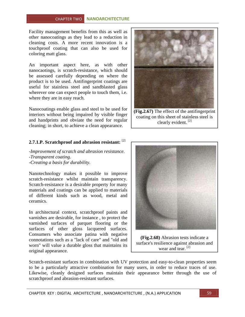
CHAPTER TWO NANOARCHITECTURE
CHAPTER KEY : DIGITAL ARCHITECTURE , NANOARCHITECTURE , (N.A.) APPLICATION 59
Facility management benefits from this as well as
other nanocoatings as they lead to a reduction in
cleaning costs. A more recent innovation is a
touchproof coating that can also be used for
coloring matt glass.
An important aspect here, as with other
nanocaotings, is scratch-resistance, which should
be assessed carefully depending on where the
product is to be used. Antifingerprint coatings are
useful for stainless steel and sandblasted glass
wherever one can expect people to touch them, i.e.
where they are in easy reach.
Nanocoatings enable glass and steel to be used for
interiors without being impaired by visible finger
and handprints and obviate the need for regular
cleaning; in short, to achieve a clean appearance.
2.7.1.P. Scratchproof and abrasion resistant: [2]
-Improvement of scratch and abrasion resistance.
-Transparent coating.
-Creating a basis for durability.
Nanotechnology makes it possible to improve
scratch-resistance whilst maintain transparency.
Scratch-resistance is a desirable property for many
materials and coatings can be applied to materials
of different kinds such as wood, metal and
ceramics.
In architectural context, scratchproof paints and
varnishes are desirable, for instance , to protect the
varnished surfaces of parquet flooring or the
surfaces of other gloss lacquered surfaces.
Consumers who associate patina with negative
connotations such as a "lack of care" and "old and
worn" will value a durable gloss that maintains its
original appearance.
Scratch-resistant surfaces in combination with UV protection and easy-to-clean properties seem
to be a particularly attractive combination for many users, in order to reduce traces of use.
Likewise, cleanly designed surfaces maintain their appearance better through the use of
scratchproof and abrasion-resistant surfaces.
(Fig.2.67) The effect of the antifingerprint
coating on this sheet of stainless steel is
clearly evident. [2]
(Fig.2.68) Abrasion tests indicate a
surface's resilience against abrasion and
wear and tear. [2]
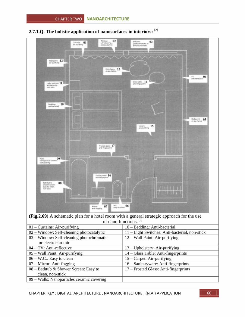
CHAPTER TWO NANOARCHITECTURE
CHAPTER KEY : DIGITAL ARCHITECTURE , NANOARCHITECTURE , (N.A.) APPLICATION 60
2.7.1.Q. The holistic application of nanosurfaces in interiors: [2]
(Fig.2.69) A schematic plan for a hotel room with a general strategic approach for the use
of nano functions. [2]
01 – Curtains: Air-purifying 10 – Bedding: Anti-bacterial 02 – Window: Self-cleaning photocatalytic 11 – Light Switches: Anti-bacterial, non-stick 03 – Window: Self-cleaning photochromatic
or electrochromic 12 – Wall Paint: Air-purifying
04 – TV: Anti-reflective 13 – Upholstery: Air-purifying 05 – Wall Paint: Air-purifying 14 – Glass Table: Anti-fingerprints 06 – W.C.: Easy to clean 15 – Carpet: Air-purifying 07 – Mirror: Anti-fogging 16 – Sanitaryware: Anti-fingerprints 08 – Bathtub & Shower Screen: Easy to
clean, non-stick 17 – Frosted Glass: Anti-fingerprints
09 – Walls: Nanoparticles ceramic covering
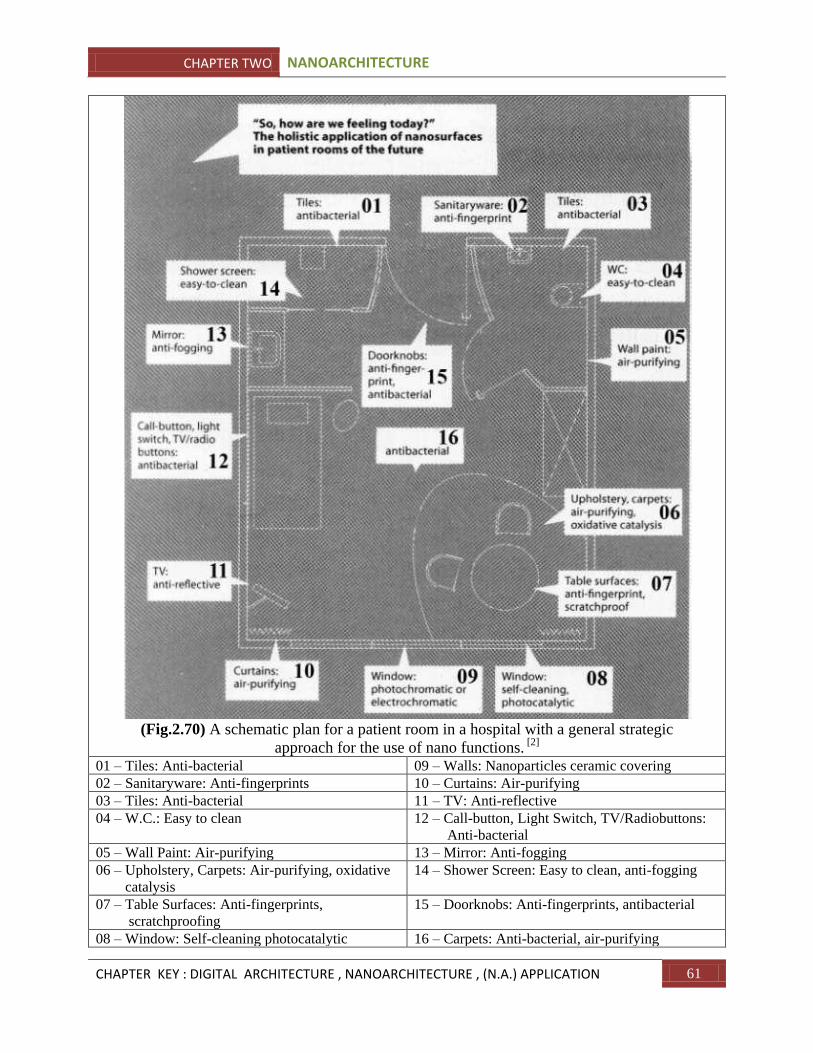
CHAPTER TWO NANOARCHITECTURE
CHAPTER KEY : DIGITAL ARCHITECTURE , NANOARCHITECTURE , (N.A.) APPLICATION 61
(Fig.2.70) A schematic plan for a patient room in a hospital with a general strategic
approach for the use of nano functions. [2]
01 – Tiles: Anti-bacterial 09 – Walls: Nanoparticles ceramic covering 02 – Sanitaryware: Anti-fingerprints 10 – Curtains: Air-purifying 03 – Tiles: Anti-bacterial 11 – TV: Anti-reflective 04 – W.C.: Easy to clean 12 – Call-button, Light Switch, TV/Radiobuttons:
Anti-bacterial 05 – Wall Paint: Air-purifying 13 – Mirror: Anti-fogging 06 – Upholstery, Carpets: Air-purifying, oxidative
catalysis
14 – Shower Screen: Easy to clean, anti-fogging
07 – Table Surfaces: Anti-fingerprints,
scratchproofing
15 – Doorknobs: Anti-fingerprints, antibacterial
08 – Window: Self-cleaning photocatalytic 16 – Carpets: Anti-bacterial, air-purifying
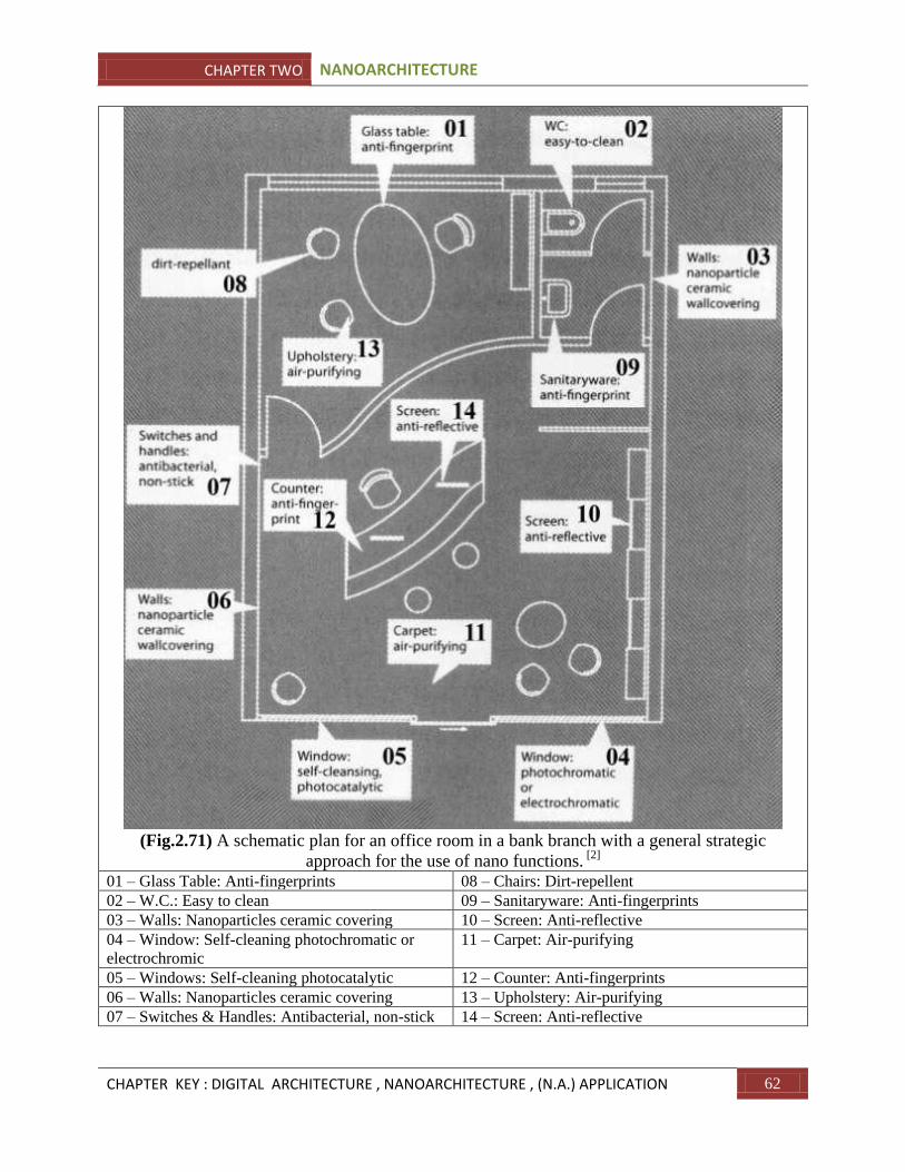
CHAPTER TWO NANOARCHITECTURE
CHAPTER KEY : DIGITAL ARCHITECTURE , NANOARCHITECTURE , (N.A.) APPLICATION 62
(Fig.2.71) A schematic plan for an office room in a bank branch with a general strategic
approach for the use of nano functions. [2]
01 – Glass Table: Anti-fingerprints 08 – Chairs: Dirt-repellent 02 – W.C.: Easy to clean 09 – Sanitaryware: Anti-fingerprints 03 – Walls: Nanoparticles ceramic covering 10 – Screen: Anti-reflective 04 – Window: Self-cleaning photochromatic or
electrochromic 11 – Carpet: Air-purifying
05 – Windows: Self-cleaning photocatalytic 12 – Counter: Anti-fingerprints 06 – Walls: Nanoparticles ceramic covering 13 – Upholstery: Air-purifying 07 – Switches & Handles: Antibacterial, non-stick 14 – Screen: Anti-reflective

CHAPTER TWO NANOARCHITECTURE
CHAPTER KEY : DIGITAL ARCHITECTURE , NANOARCHITECTURE , (N.A.) APPLICATION 63
Nano functions have been employed in interior design only occasionally if at all, and more or
less by chance. Three schematic plans for a hotel room, a room in a clinic or hospital and an
office room in a bank branch demonstrate concepts for a general strategic approach to using nano
functions in interior design.
The overall concept varies depending on the respective needs of the different uses. The spaces
are optimized through the strategic use of nanosurfaces with regard to aesthetic, economical and
ecological concerns.
Improved comfort and cost-effectiveness go hand in hand. Cost assessments should take account
not only of the initial expenditure but also the follow-on costs, which are reduced considerably.
Despite the fact that these are visionary concepts, they could already be realized today in this or a
similar form.
2.3.3.R. Next Generation Building Cleaning Solution: [35]
Objective: Building exterior self cleaning, protection and energy saving Road self-cleaning,
protection and car exhausts purification
Solution: Gens Nano photocatalyst coating is the combination of photocatalyst and nano
technology. Just simple application of Gens Nano coating on the building exterior
surface will bring diversified excellent features to the building.
Also, coating can be sprayed on highway barriers and side walks to provide the
self-cleaning & air purification function. Gens Nano coating can keep the
surfaces in a very new look and reduce the cleaning & maintenance costs.
Features: - Super hydrophilicity
- Air purification
- Anti-bacterial and anti-mold
- UV damage protection
- Surface antistatic
- Self-cleaning
- Easy-cleaning
Benefits: - Keeps the building clean
- Protects the surface from dust, acid rain and air pollutant damage
- Purifies the air pollutants near and on the surface
(e.g. car exhausts, NOx, Formaldehyde, Benzene, VOCs)
- Decomposes the organic pollutants on the surface.
- Makes the surface without water stain after raining
- Reduces the energy consumption for cooling building in summer
- Restrains mildew or alga from growing
- Kills bacteria and virus on the surface and in the air near the coated building
- Absorbs UV rays from sun and protects the surface from UV damage
- Restrains the dust electrostatic adsorption

CHAPTER TWO NANOARCHITECTURE
CHAPTER KEY : DIGITAL ARCHITECTURE , NANOARCHITECTURE , (N.A.) APPLICATION 64
Example 1. Exterior wall self-cleaning : [35]
Surface Granite Application by spray
Product Nano photocatalyst coating Period 3 months
This picture shows a granite wall which has
become old and dirty after years of weathering.
The area divided by yellow adhesive tape will be
coated with photocatalyst sol later.
Before photocatalyst coating is applied on the
surface, proper pre-cleaning work is necessary.
We applied photocatalyst on the left part of the
cleaned area.
After 3 months of weathering, the wall on the left
side coated with photocatalyst shows the results of
our self-cleaning product.
The uncoated area on the right side becomes dirty
and dark due to the poor air quality and pollution.
(Fig.2.72.A) This picture shows a granite
wall which has become
old and dirty after years of weathering.
(Photo #1 dated Dec. 14th 2005). [35]
(Fig.2.72.B) Before photocatalyst coating
is applied on the surface, proper pre-
cleaning work is necessary.
(Photo #2 dated Dec. 14th 2005). [35]
(Fig.2.72.C) After 3 months of
weathering.
(Photo #3 dated Mar. 15th 2006). [35]
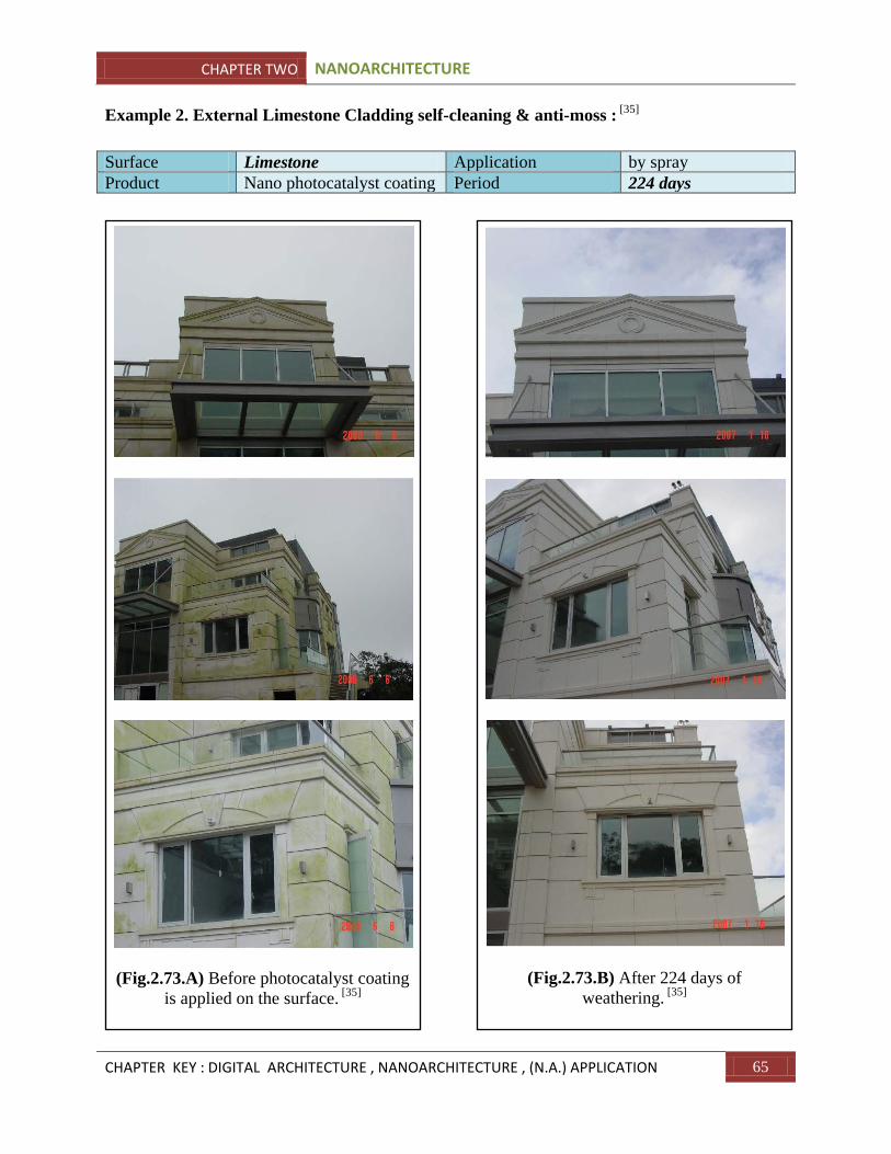
CHAPTER TWO NANOARCHITECTURE
CHAPTER KEY : DIGITAL ARCHITECTURE , NANOARCHITECTURE , (N.A.) APPLICATION 65
Example 2. External Limestone Cladding self-cleaning & anti-moss : [35]
Surface Limestone Application by spray
Product Nano photocatalyst coating Period 224 days
(Fig.2.73.B) After 224 days of
weathering. [35]
(Fig.2.73.A) Before photocatalyst coating
is applied on the surface. [35]
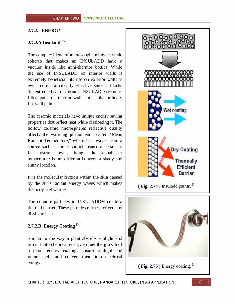
CHAPTER TWO NANOARCHITECTURE
CHAPTER KEY : DIGITAL ARCHITECTURE , NANOARCHITECTURE , (N.A.) APPLICATION 66
2.7.2. ENERGY
2.7.2.A Insuladd [34]
The complex blend of microscopic hollow ceramic
spheres that makes up INSULADD have a
vacuum inside like mini-thermos bottles. While
the use of INSULADD on interior walls is
extremely beneficial, its use on exterior walls is
even more dramatically effective since it blocks
the extreme heat of the sun. INSULADD ceramic-
filled paint on interior walls looks like ordinary
flat wall paint.
The ceramic materials have unique energy saving
properties that reflect heat while dissipating it. The
hollow ceramic microspheres reflective quality
affects the warming phenomenon called "Mean
Radiant Temperature," where heat waves from a
source such as direct sunlight cause a person to
feel warmer even though the actual air
temperature is not different between a shady and
sunny location.
It is the molecular friction within the skin caused
by the sun's radiant energy waves which makes
the body feel warmer.
The ceramic particles in INSULADD® create a
thermal barrier. These particles refract, reflect, and
dissipate heat.
2.7.2.B. Energy Coating [34]
Similar to the way a plant absorbs sunlight and
turns it into chemical energy to fuel the growth of
a plant, energy coatings absorb sunlight and
indoor light and convert them into electrical
energy.
( Fig. 2.74 ) Insuladd paints. [34]
( Fig. 2.75 ) Energy coating. [34]
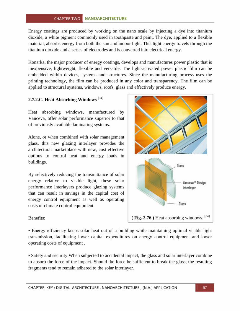
CHAPTER TWO NANOARCHITECTURE
CHAPTER KEY : DIGITAL ARCHITECTURE , NANOARCHITECTURE , (N.A.) APPLICATION 67
Energy coatings are produced by working on the nano scale by injecting a dye into titanium
dioxide, a white pigment commonly used in toothpaste and paint. The dye, applied to a flexible
material, absorbs energy from both the sun and indoor light. This light energy travels through the
titanium dioxide and a series of electrodes and is converted into electrical energy.
Konarka, the major producer of energy coatings, develops and manufactures power plastic that is
inexpensive, lightweight, flexible and versatile. The light-activated power plastic film can be
embedded within devices, systems and structures. Since the manufacturing process uses the
printing technology, the film can be produced in any color and transparency. The film can be
applied to structural systems, windows, roofs, glass and effectively produce energy.
2.7.2.C. Heat Absorbing Windows [34]
Heat absorbing windows, manufactured by
Vanceva, offer solar performance superior to that
of previously available laminating systems.
Alone, or when combined with solar management
glass, this new glazing interlayer provides the
architectural marketplace with new, cost effective
options to control heat and energy loads in
buildings.
By selectively reducing the transmittance of solar
energy relative to visible light, these solar
performance interlayers produce glazing systems
that can result in savings in the capital cost of
energy control equipment as well as operating
costs of climate control equipment.
Benefits:
• Energy efficiency keeps solar heat out of a building while maintaining optimal visible light
transmission, facilitating lower capital expenditures on energy control equipment and lower
operating costs of equipment .
• Safety and security When subjected to accidental impact, the glass and solar interlayer combine
to absorb the force of the impact. Should the force be sufficient to break the glass, the resulting
fragments tend to remain adhered to the solar interlayer.
( Fig. 2.76 ) Heat absorbing windows. [34]
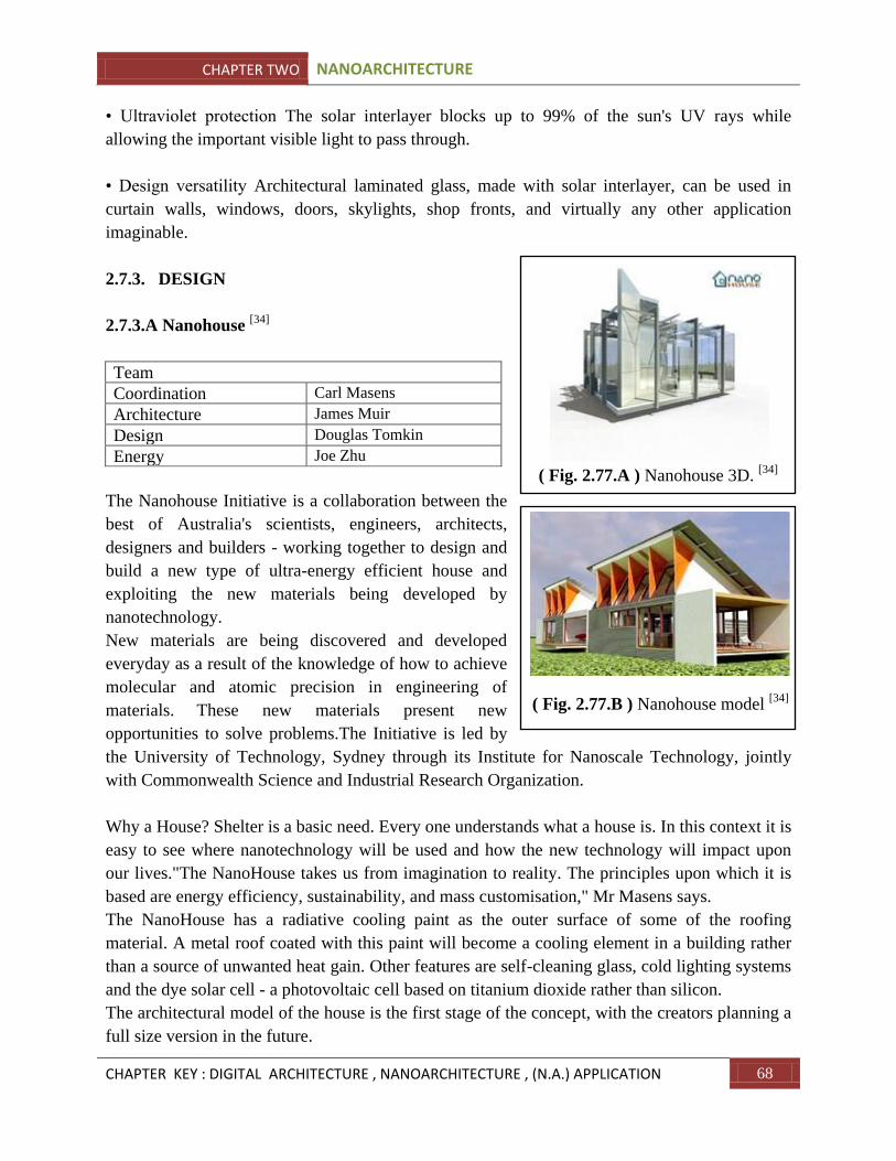
CHAPTER TWO NANOARCHITECTURE
CHAPTER KEY : DIGITAL ARCHITECTURE , NANOARCHITECTURE , (N.A.) APPLICATION 68
• Ultraviolet protection The solar interlayer blocks up to 99% of the sun's UV rays while
allowing the important visible light to pass through.
• Design versatility Architectural laminated glass, made with solar interlayer, can be used in
curtain walls, windows, doors, skylights, shop fronts, and virtually any other application
imaginable.
2.7.3. DESIGN
2.7.3.A Nanohouse [34]
Team
Coordination Carl Masens
Architecture James Muir
Design Douglas Tomkin
Energy Joe Zhu
The Nanohouse Initiative is a collaboration between the
best of Australia's scientists, engineers, architects,
designers and builders - working together to design and
build a new type of ultra-energy efficient house and
exploiting the new materials being developed by
nanotechnology.
New materials are being discovered and developed
everyday as a result of the knowledge of how to achieve
molecular and atomic precision in engineering of
materials.
These new materials present new
opportunities to solve problems.The Initiative is led by
the University of Technology, Sydney through its Institute for Nanoscale Technology, jointly
with Commonwealth Science and Industrial Research Organization.
Why a House? Shelter is a basic need. Every one understands what a house is. In this context it is
easy to see where nanotechnology will be used and how the new technology will impact upon
our lives."The NanoHouse takes us from imagination to reality. The principles upon which it is
based are energy efficiency, sustainability, and mass customisation," Mr Masens says.
The NanoHouse has a radiative cooling paint as the outer surface of some of the roofing
material. A metal roof coated with this paint will become a cooling element in a building rather
than a source of unwanted heat gain. Other features are self-cleaning glass, cold lighting systems
and the dye solar cell - a photovoltaic cell based on titanium dioxide rather than silicon.
The architectural model of the house is the first stage of the concept, with the creators planning a
full size version in the future.
( Fig. 2.77.A ) Nanohouse 3D. [34]
( Fig. 2.77.B ) Nanohouse model [34]
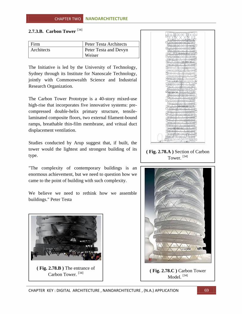
CHAPTER TWO NANOARCHITECTURE
CHAPTER KEY : DIGITAL ARCHITECTURE , NANOARCHITECTURE , (N.A.) APPLICATION 69
2.7.3.B. Carbon Tower [34]
Firm Peter Testa Architects
Architects Peter Testa and Devyn
Weiser
The Initiative is led by the University of Technology,
Sydney through its Institute for Nanoscale Technology,
jointly with Commonwealth Science and Industrial
Research Organization.
The Carbon Tower Prototype is a 40-story mixed-use
high-rise that incorporates five innovative systems: pre-
compressed double-helix primary structure, tensile-
laminated composite floors, two external filament-bound
ramps, breathable thin-film membrane, and vritual duct
displacement ventilation.
Studies conducted by Arup suggest that, if built, the
tower would the lightest and strongest building of its
type.
"The complexity of contemporary buildings is an
enormous achievement, but we need to question how we
came to the point of building with such complexity.
We believe we need to rethink how we assemble
buildings." Peter Testa
( Fig. 2.78.C ) Carbon Tower
Model. [34]
( Fig. 2.78.A ) Section of Carbon
Tower. [34]
( Fig. 2.78.B ) The entrance of
Carbon Tower. [34]
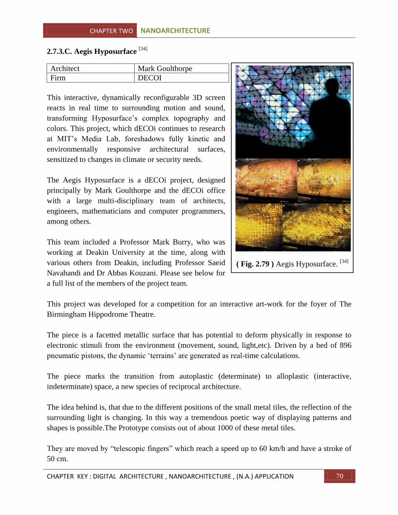
CHAPTER TWO NANOARCHITECTURE
CHAPTER KEY : DIGITAL ARCHITECTURE , NANOARCHITECTURE , (N.A.) APPLICATION 70
2.7.3.C. Aegis Hyposurface [34]
Architect Mark Goulthorpe
Firm DECOI
This interactive, dynamically reconfigurable 3D screen
reacts in real time to surrounding motion and sound,
transforming Hyposurface‟s complex topography and
colors. This project, which dECOi continues to research
at MIT‟s Media Lab, foreshadows fully kinetic and
environmentally responsive architectural surfaces,
sensitized to changes in climate or security needs.
The Aegis Hyposurface is a dECOi project, designed
principally by Mark Goulthorpe and the dECOi office
with a large multi-disciplinary team of architects,
engineers, mathematicians and computer programmers,
among others.
This team included a Professor Mark Burry, who was
working at Deakin University at the time, along with
various others from Deakin, including Professor Saeid
Navahandi and Dr Abbas Kouzani. Please see below for
a full list of the members of the project team.
This project was developed for a competition for an interactive art-work for the foyer of The
Birmingham Hippodrome Theatre.
The piece is a facetted metallic surface that has potential to deform physically in response to
electronic stimuli from the environment (movement, sound, light,etc). Driven by a bed of 896
pneumatic pistons, the dynamic „terrains‟ are generated as real-time calculations.
The piece marks the transition from autoplastic (determinate) to alloplastic (interactive,
indeterminate) space, a new species of reciprocal architecture.
The idea behind is, that due to the different positions of the small metal tiles, the reflection of the
surrounding light is changing. In this way a tremendous poetic way of displaying patterns and
shapes is possible.The Prototype consists out of about 1000 of these metal tiles.
They are moved by “telescopic fingers” which reach a speed up to 60 km/h and have a stroke of
50 cm.
( Fig. 2.79 ) Aegis Hyposurface. [34]
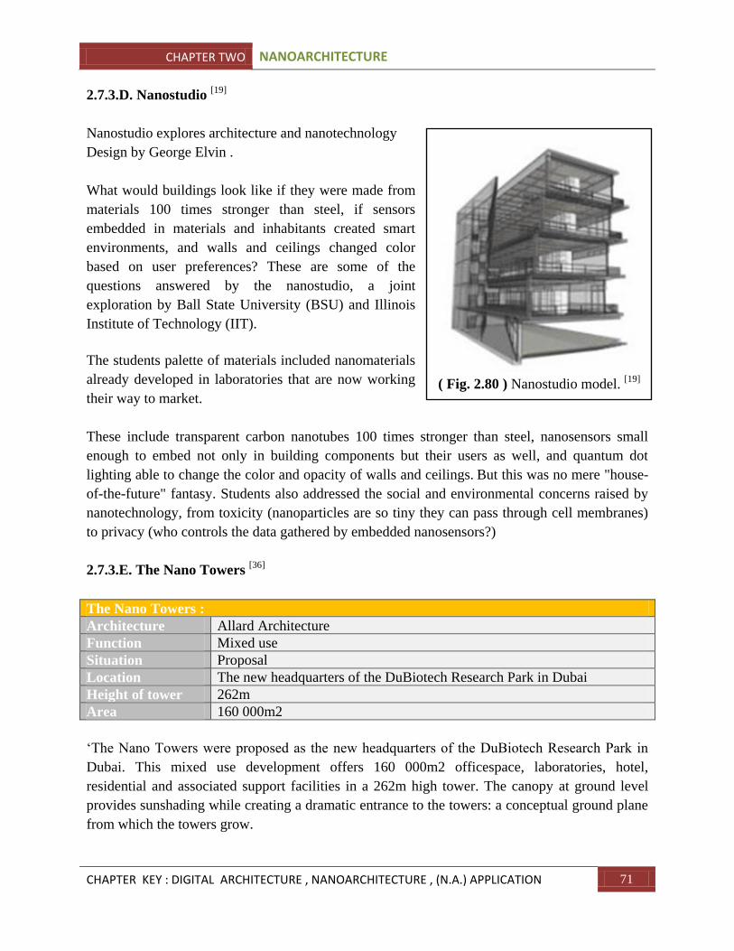
CHAPTER TWO NANOARCHITECTURE
CHAPTER KEY : DIGITAL ARCHITECTURE , NANOARCHITECTURE , (N.A.) APPLICATION 71
2.7.3.D. Nanostudio [19]
Nanostudio explores architecture and nanotechnology
Design by George Elvin .
What would buildings look like if they were made from
materials 100 times stronger than steel, if sensors
embedded in materials and inhabitants created smart
environments, and walls and ceilings changed color
based on user preferences? These are some of the
questions answered by the nanostudio, a joint
exploration by Ball State University (BSU) and Illinois
Institute of Technology (IIT).
The students palette of materials included nanomaterials
already developed in laboratories that are now working
their way to market.
These include transparent carbon nanotubes 100 times stronger than steel, nanosensors small
enough to embed not only in building components but their users as well, and quantum dot
lighting able to change the color and opacity of walls and ceilings. But this was no mere "house-
of-the-future" fantasy. Students also addressed the social and environmental concerns raised by
nanotechnology, from toxicity (nanoparticles are so tiny they can pass through cell membranes)
to privacy (who controls the data gathered by embedded nanosensors?)
2.7.3.E. The Nano Towers [36]
The Nano Towers :
Architecture Allard Architecture
Function Mixed use
Situation Proposal
Location The new headquarters of the DuBiotech Research Park in Dubai
Height of tower 262m
Area 160 000m2
„The Nano Towers were proposed as the new headquarters of the DuBiotech Research Park in
Dubai. This mixed use development offers 160 000m2 officespace, laboratories, hotel,
residential and associated support facilities in a 262m high tower. The canopy at ground level
provides sunshading while creating a dramatic entrance to the towers: a conceptual ground plane
from which the towers grow.
( Fig. 2.80 ) Nanostudio model. [19]
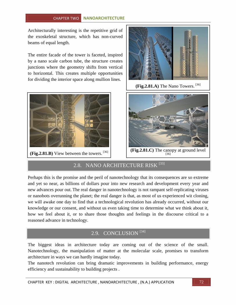
CHAPTER TWO NANOARCHITECTURE
CHAPTER KEY : DIGITAL ARCHITECTURE , NANOARCHITECTURE , (N.A.) APPLICATION 72
Architecturally interesting is the repetitive grid of
the exoskeletal structure, which has non-curved
beams of equal length.
The entire facade of the tower is faceted, inspired
by a nano scale carbon tube, the structure creates
junctions where the geometry shifts from vertical
to horizontal. This creates multiple opportunities
for dividing the interior space along mullion lines.
Perhaps this is the promise and the peril of nanotechnology that its consequences are so extreme
and yet so near, as billions of dollars pour into new research and development every year and
new advances pour out. The real danger in nanotechnology is not rampant self-replicating viruses
or nanobots overunning the planet; the real danger is that, as most of us experienced wit cloning,
we will awake one day to find that a technological revolution has already occurred, without our
knowledge or our consent, and without us even taking time to determine what we think about it,
how we feel about it, or to share those thoughts and feelings in the discourse critical to a
reasoned advance in technology.
The biggest ideas in architecture today are coming out of the science of the small.
Nanotechnology, the manipulation of matter at the molecular scale, promises to transform
architecture in ways we can hardly imagine today.
The nanotech revolution can bring dramatic improvements in building performance, energy
efficiency and sustainability to building projects .
(Fig.2.81.A) The Nano Towers. [36]
(Fig.2.81.C) The canopy at ground level
[36]
(Fig.2.81.B) View between the towers. [36]
2.8. NANO ARCHITECTURE RISK [33]
2.9. CONCLUSION [34]

CHAPTER THREE
GREEN NANOARCHITECTURE
G R E E N
N A N O A R C H I T E C T U R E
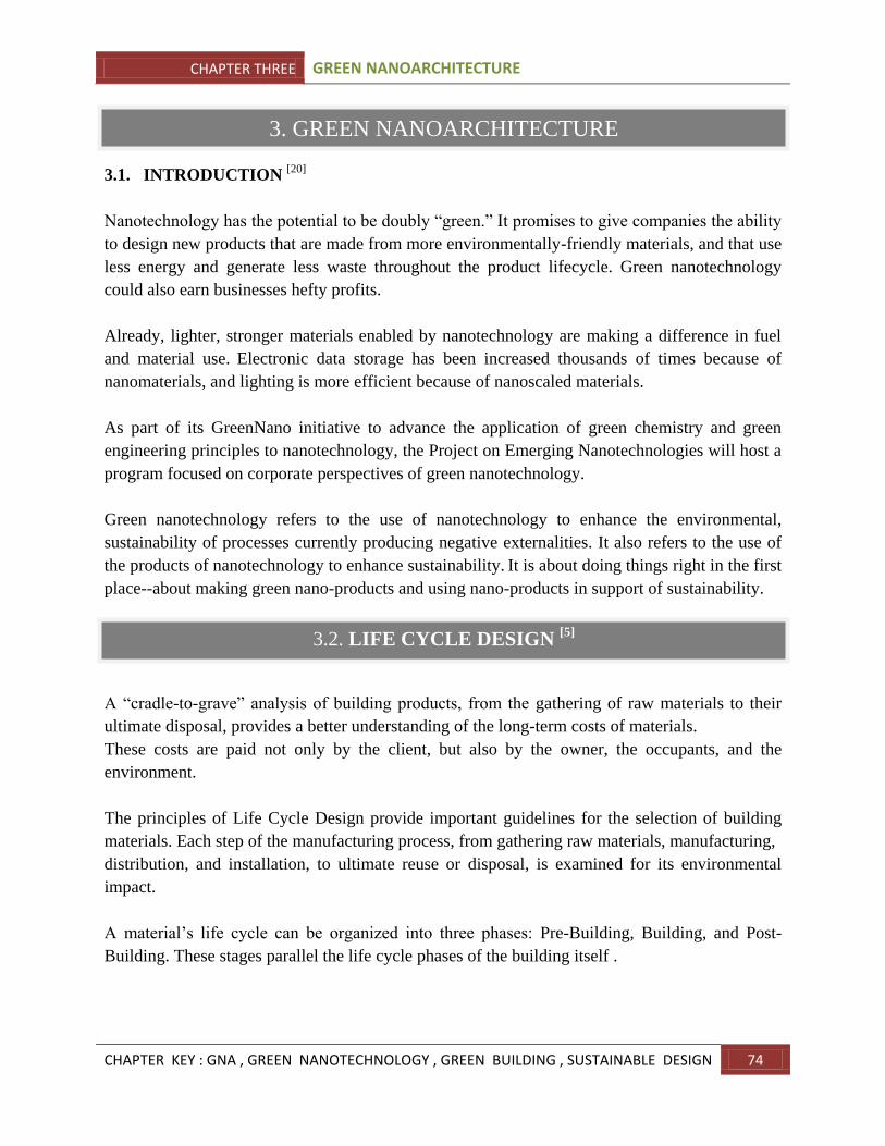
CHAPTER THREE GREEN NANOARCHITECTURE
CHAPTER KEY : GNA , GREEN NANOTECHNOLOGY , GREEN BUILDING , SUSTAINABLE DESIGN 74
3.1. INTRODUCTION [20]
Nanotechnology has the potential to be doubly “green.” It promises to give companies the ability
to design new products that are made from more environmentally-friendly materials, and that use
less energy and generate less waste throughout the product lifecycle. Green nanotechnology
could also earn businesses hefty profits.
Already, lighter, stronger materials enabled by nanotechnology are making a difference in fuel
and material use. Electronic data storage has been increased thousands of times because of
nanomaterials, and lighting is more efficient because of nanoscaled materials.
As part of its GreenNano initiative to advance the application of green chemistry and green
engineering principles to nanotechnology, the Project on Emerging Nanotechnologies will host a
program focused on corporate perspectives of green nanotechnology.
Green nanotechnology refers to the use of nanotechnology to enhance the environmental,
sustainability of processes currently producing negative externalities. It also refers to the use of
the products of nanotechnology to enhance sustainability. It is about doing things right in the first
place--about making green nano-products and using nano-products in support of sustainability.
A “cradle-to-grave” analysis of building products, from the gathering of raw materials to their
ultimate disposal, provides a better understanding of the long-term costs of materials.
These costs are paid not only by the client, but also by the owner, the occupants, and the
environment.
The principles of Life Cycle Design provide important guidelines for the selection of building
materials. Each step of the manufacturing process, from gathering raw materials, manufacturing,
distribution, and installation, to ultimate reuse or disposal, is examined for its environmental
impact.
A material‟s life cycle can be organized into three phases: Pre-Building, Building, and Post-
Building. These stages parallel the life cycle phases of the building itself .
3. GREEN NANOARCHITECTURE
3.2. LIFE CYCLE DESIGN [5]
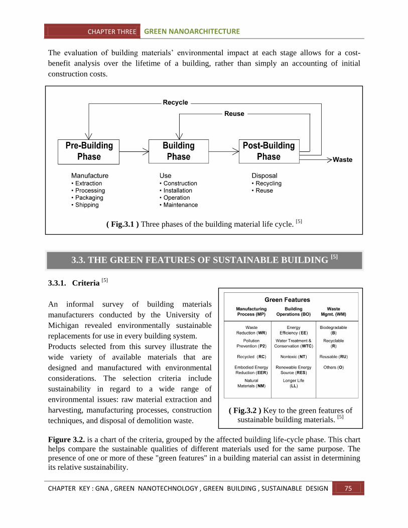
CHAPTER THREE GREEN NANOARCHITECTURE
CHAPTER KEY : GNA , GREEN NANOTECHNOLOGY , GREEN BUILDING , SUSTAINABLE DESIGN 75
The evaluation of building materials‟ environmental impact at each stage allows for a cost-
benefit analysis over the lifetime of a building, rather than simply an accounting of initial
construction costs.
3.3.1. Criteria [5]
An informal survey of building materials
manufacturers conducted by the University of
Michigan revealed environmentally sustainable
replacements for use in every building system.
Products selected from this survey illustrate the
wide variety of available materials that are
designed and manufactured with environmental
considerations. The selection criteria include
sustainability in regard to a wide range of
environmental issues: raw material extraction and
harvesting, manufacturing processes, construction
techniques, and disposal of demolition waste.
Figure 3.2. is a chart of the criteria, grouped by the affected building life-cycle phase. This chart
helps compare the sustainable qualities of different materials used for the same purpose. The
presence of one or more of these "green features" in a building material can assist in determining
its relative sustainability.
( Fig.3.1 ) Three phases of the building material life cycle. [5]
3.3. THE GREEN FEATURES OF SUSTAINABLE BUILDING [5]
MATERIALS
( Fig.3.2 ) Key to the green features of
sustainable building materials. [5]
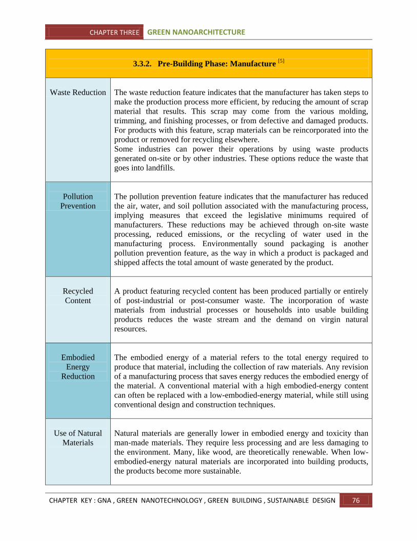
CHAPTER THREE GREEN NANOARCHITECTURE
CHAPTER KEY : GNA , GREEN NANOTECHNOLOGY , GREEN BUILDING , SUSTAINABLE DESIGN 76
3.3.2. Pre-Building Phase: Manufacture [5]
Waste Reduction
The waste reduction feature indicates that the manufacturer has taken steps to
make the production process more efficient, by reducing the amount of scrap
material that results. This scrap may come from the various molding,
trimming, and finishing processes, or from defective and damaged products.
For products with this feature, scrap materials can be reincorporated into the
product or removed for recycling elsewhere.
Some industries can power their operations by using waste products
generated on-site or by other industries. These options reduce the waste that
goes into landfills.
Pollution
Prevention
The pollution prevention feature indicates that the manufacturer has reduced
the air, water, and soil pollution associated with the manufacturing process,
implying measures that exceed the legislative minimums required of
manufacturers. These reductions may be achieved through on-site waste
processing, reduced emissions, or the recycling of water used in the
manufacturing process. Environmentally sound packaging is another
pollution prevention feature, as the way in which a product is packaged and
shipped affects the total amount of waste generated by the product.
Recycled
Content
A product featuring recycled content has been produced partially or entirely
of post-industrial or post-consumer waste. The incorporation of waste
materials from industrial processes or households into usable building
products reduces the waste stream and the demand on virgin natural
resources.
Embodied
Energy
Reduction
The embodied energy of a material refers to the total energy required to
produce that material, including the collection of raw materials. Any revision
of a manufacturing process that saves energy reduces the embodied energy of
the material. A conventional material with a high embodied-energy content
can often be replaced with a low-embodied-energy material, while still using
conventional design and construction techniques.
Use of Natural
Materials
Natural materials are generally lower in embodied energy and toxicity than
man-made materials. They require less processing and are less damaging to
the environment. Many, like wood, are theoretically renewable. When low-
embodied-energy natural materials are incorporated into building products,
the products become more sustainable.
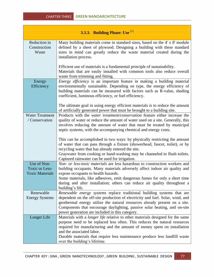
CHAPTER THREE GREEN NANOARCHITECTURE
CHAPTER KEY : GNA , GREEN NANOTECHNOLOGY , GREEN BUILDING , SUSTAINABLE DESIGN 77
3.3.3. Building Phase: Use [5]
Reduction in
Construction
Waste
Many building materials come in standard sizes, based on the 4' x 8' module
defined by a sheet of plywood. Designing a building with these standard
sizes in mind can greatly reduce the waste material created during the
installation process.
Efficient use of materials is a fundamental principle of sustainability.
Materials that are easily installed with common tools also reduce overall
waste from trimming and fitting.
Energy
Efficiency
Energy efficiency is an important feature in making a building material
environmentally sustainable. Depending on type, the energy efficiency of
building materials can be measured with factors such as R-value, shading
coefficient, luminous efficiency, or fuel efficiency.
The ultimate goal in using energy efficient materials is to reduce the amount
of artificially generated power that must be brought to a building site.
Water Treatment
/ Conservation
Products with the water treatment/conservation feature either increase the
quality of water or reduce the amount of water used on a site. Generally, this
involves reducing the amount of water that must be treated by municipal
septic systems, with the accompanying chemical and energy costs.
This can be accomplished in two ways: by physically restricting the amount
of water that can pass through a fixture (showerhead, faucet, toilet), or by
recycling water that has already entered the site.
Graywater from cooking or hand-washing may be channeled to flush toilets.
Captured rainwater can be used for irrigation.
Use of Non-
Toxic or Less-
Toxic Materials
Non- or less-toxic materials are less hazardous to construction workers and
building occupants. Many materials adversely affect indoor air quality and
expose occupants to health hazards.
Some materials, like adhesives, emit dangerous fumes for only a short time
during and after installation; others can reduce air quality throughout a
building‟s life.
Renewable
Energy Systems
Renewable energy systems replace traditional building systems that are
dependent on the off-site production of electricity and fuel. Solar, wind, and
geothermal energy utilize the natural resources already present on a site.
Components that encourage daylighting, passive solar heating, and on-site
power generation are included in this category.
Longer Life Materials with a longer life relative to other materials designed for the same
purpose need to be replaced less often. This reduces the natural resources
required for manufacturing and the amount of money spent on installation
and the associated labor.
Durable materials that require less maintenance produce less landfill waste
over the building‟s lifetime.
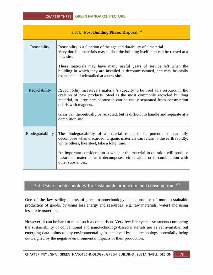
CHAPTER THREE GREEN NANOARCHITECTURE
CHAPTER KEY : GNA , GREEN NANOTECHNOLOGY , GREEN BUILDING , SUSTAINABLE DESIGN 78
3.3.4. Post-Building Phase: Disposal [5]
Reusability
Reusability is a function of the age and durability of a material.
Very durable materials may outlast the building itself, and can be reused at a
new site.
These materials may have many useful years of service left when the
building in which they are installed is decommissioned, and may be easily
extracted and reinstalled at a new site.
Recyclability
Recyclability measures a material‟s capacity to be used as a resource in the
creation of new products. Steel is the most commonly recycled building
material, in large part because it can be easily separated from construction
debris with magnets.
Glass can theoretically be recycled, but is difficult to handle and separate at a
demolition site.
Biodegradability
The biodegradability of a material refers to its potential to naturally
decompose when discarded. Organic materials can return to the earth rapidly,
while others, like steel, take a long time.
An important consideration is whether the material in question will produce
hazardous materials as it decomposes, either alone or in combination with
other substances.
One of the key selling points of green nanotechnology is its promise of more sustainable
production of goods, by using less energy and resources (e.g. raw materials, water) and using
less toxic materials.
However, it can be hard to make such a comparison. Very few life cycle assessments comparing
the sustainability of conventional and nanotechnology-based materials are as yet available, but
emerging data points to any environmental gains achieved by nanotechnology potentially being
outweighed by the negative environmental impacts of their production.
3.4. Using nanotechnology for sustainable production and consumption [42]
CHAPTER THREE GREEN NANOARCHITECTURE
CHAPTER KEY : GNA , GREEN NANOTECHNOLOGY , GREEN BUILDING , SUSTAINABLE DESIGN 79
GREEN NANOTECHNOLOGY + ARCHITECTURE = GREEN NANOARCHITECTURE
Green nanotechnology is the development of clean technologies, "to minimize potential
environmental and human health risks associated with the manufacture and use of
nanotechnology products, and to encourage replacement of existing products with new nano-
products that are more environmentally friendly throughout their lifecycle."
Green Nanotechnology has two goals: producing nanomaterials and products without harming
the environment or human health, and producing nano-products that provide solutions to
environmental problems. It uses existing principles of Green Chemistry and Green Engineering
to make nanomaterials and nano-products without toxic ingredients, at low temperatures using
less energy and renewable inputs wherever possible, and using lifecycle thinking in all design
and engineering stages. In addition to making nanomaterials and products with less impact to the
environment, Green Nanotechnology also means using nanotechnology to make current
manufacturing processes for non-nano materials and products more environmentally friendly.
For example, nanoscale membranes can help separate desired chemical reaction products from
waste materials.
Nanoscale catalysts can make chemical reactions more efficient and less wasteful. Sensors at the
nanoscale can form a part of process control systems, working with nano-enabled information
systems. Using alternative energy systems, made possible by nanotechnology, is another way to
"green" manufacturing processes.
The second goal of Green Nanotechnology involves developing products that benefit the
environment either directly or indirectly.Nanomaterials or products directly can clean hazardous
waste sites, desalinate water, treat pollutants, or sense and monitor environmental pollutants.
Indirectly, lightweight nanocomposites for automobiles and other means of transportation could
save fuel and reduce materials used for production; nanotechnology-enabled fuel cells and light-
emitting diodes (LEDs) could reduce pollution from energy generation and help conserve fossil
fuels; self-cleaning nanoscale surface coatings could reduce or eliminate many cleaning
chemicals; and enhanced battery life could lead to less material use and less waste.
Green Nanotechnology takes a broad systems view of nanomaterials and products, ensuring that
unforeseen consequences are minimized and that impacts are anticipated throughout the full life
cycle.
3.5. DEFINITION OF GREEN NANOARCHITECTURE (GNA) [21]
3.6. GREEN NANO TECHNOLOGY GOALS [21]
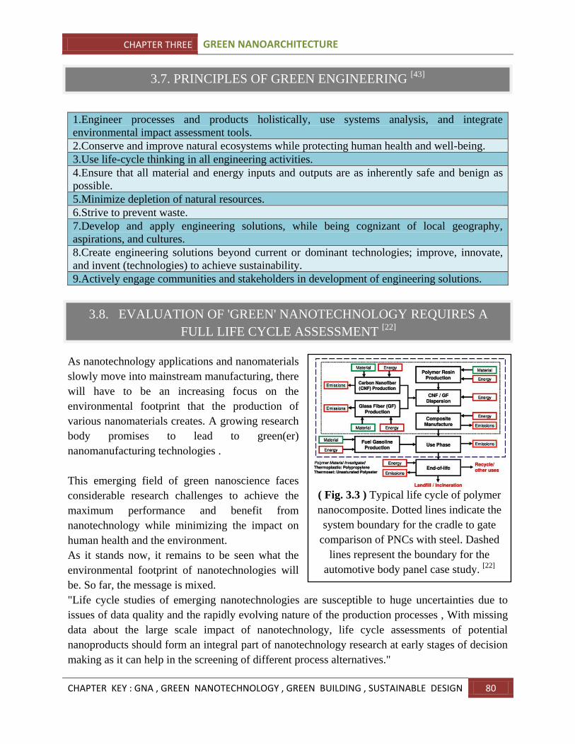
CHAPTER THREE GREEN NANOARCHITECTURE
CHAPTER KEY : GNA , GREEN NANOTECHNOLOGY , GREEN BUILDING , SUSTAINABLE DESIGN 80
1.Engineer processes and products holistically, use systems analysis, and integrate
environmental impact assessment tools.
2.Conserve and improve natural ecosystems while protecting human health and well-being.
3.Use life-cycle thinking in all engineering activities.
4.Ensure that all material and energy inputs and outputs are as inherently safe and benign as
possible.
5.Minimize depletion of natural resources.
6.Strive to prevent waste.
7.Develop and apply engineering solutions, while being cognizant of local geography,
aspirations, and cultures.
8.Create engineering solutions beyond current or dominant technologies; improve, innovate,
and invent (technologies) to achieve sustainability.
9.Actively engage communities and stakeholders in development of engineering solutions.
As nanotechnology applications and nanomaterials
slowly move into mainstream manufacturing, there
will have to be an increasing focus on the
environmental footprint that the production of
various nanomaterials creates. A growing research
body promises to lead to green(er)
nanomanufacturing technologies .
This emerging field of green nanoscience faces
considerable research challenges to achieve the
maximum performance and benefit from
nanotechnology while minimizing the impact on
human health and the environment.
As it stands now, it remains to be seen what the
environmental footprint of nanotechnologies will
be. So far, the message is mixed.
"Life cycle studies of emerging nanotechnologies are susceptible to huge uncertainties due to
issues of data quality and the rapidly evolving nature of the production processes , With missing
data about the large scale impact of nanotechnology, life cycle assessments of potential
nanoproducts should form an integral part of nanotechnology research at early stages of decision
making as it can help in the screening of different process alternatives."
3.7. PRINCIPLES OF GREEN ENGINEERING [43]
3.8. EVALUATION OF 'GREEN' NANOTECHNOLOGY REQUIRES A
FULL LIFE CYCLE ASSESSMENT [22]
( Fig. 3.3 ) Typical life cycle of polymer
nanocomposite. Dotted lines indicate the
system boundary for the cradle to gate
comparison of PNCs with steel. Dashed
lines represent the boundary for the
automotive body panel case study. [22]
CHAPTER THREE GREEN NANOARCHITECTURE
CHAPTER KEY : GNA , GREEN NANOTECHNOLOGY , GREEN BUILDING , SUSTAINABLE DESIGN 81
Nanotechnology is all about getting more function on less space. Efficiency and getting more
with less is essential for sustainability. How can nanotechnology contribute to making energy
conversion and energy storage more efficient or improving product durability?
More for less: Nanotechnology is about getting more function on less space. Efficiency and
getting more with less is essential for sustainability. Nanotechnology is also about integrating
disciplines and building a cross disciplinary research community. New solutions to replace non-
renewable energy based technologies and minimize their impact on the environment will need
this cross disciplinary approach. Nanotechnology can contribute to making energy conversion
and energy storage more efficient or improving product durability. Catalyst design can improve
H2 production, nanoparticles as fuel additive can reduce waste gas emission, nanostructured
materials can be used for direct energy conversion or to improve photovoltaic cells, electrodes
and membranes for fuel cells or improve lighting.
Carbon nanotubes provide atomically smooth channels with unprecedented properties for water
purification.They can at the same time be used for light weight, high strength composites for
future cars and planes that may consume less energy and be more efficient.
Nanoparticles based on biomimetic systems can be used to clean up waste. Increasing population
and pollution levels has already started to affect the food industry. Nanotechnology will impact
how food is grown, processed and packed or can be used to reduce pesticides. These are all
potential contributions of nanotechnology to sustainability. A lot of it is not yet real but there is a
significant potential.
3.9.1. Nanotechnology and clean technology [23]
This year‟s 10th NSTI nanotechnology conference in Santa Clara teamed up with the first
conference on clean technology . „CleanTech‟ has become a buzz word that is increasingly
gaining attention since sustainability is an issue in the context of global warming, climate change
and increasing cost of primary natural resources. [14]
The issue of sustainability has clearly caught
the interest of the economic world. A strong support from the venture capital community in
California can be traced to the fact that the long term perspective for any clean technology is
very stable .
Any new technology is however expensive at the beginning. But increasing energy cost and the
cost of other natural resources make alternative energy sources and intelligent solutions more
cost competitive while mass production of the new technology helps to drive costs down.
3.9. NANOTECHNOLOGY , GREEN BUILDING AND SUSTAINABLE
DESIGN [23]
CHAPTER THREE GREEN NANOARCHITECTURE
CHAPTER KEY : GNA , GREEN NANOTECHNOLOGY , GREEN BUILDING , SUSTAINABLE DESIGN 82
3.9.2. Energy and big things start small [23]
One of the main issues about sustainability is the way we use energy. We use mostly non-
renewable energy. The main demand of sustainable technology is that it makes a radical shift
towards the use of renewable energy.
There is plenty of sun energy shining on us and we have yet to learn how to make use of it. How
can energy conversion and energy storage be improved? How can energy consumption be
reduced through intelligent design or by intelligent system integration? We could imagine a
system where mechanical energy is converted into electrical energy, stored as chemical energy
and is recovered on demand.
The roofs of our buildings could be covered with solar panels or collectors to convert sun light
into thermal or electrical energy. Sun collectors combined with a Sterling engine show promising
results . Electricity might soon flow in the installations of our house in both directions. [14]
Surplus energy from our roofs will provide electricity to the grid reducing overall consumption
of non-renewable energy sources.
3.9.3. Facing facts [23]
Nanotechnology has the potential to make a big impact on sustainability. But this will need a
multiple of cross disciplinary approaches to solve main issues that resulted from 150 years of
massive industrialization.
It is not enough that a scientist makes a discovery when industry is based on non-renewable
natural resources; it is not enough to design new products without knowing what is going to
happen to it at the end of its lifetime.
Today, Sustainability is the biggest challenge that humans face.
3.10.1. NANO CITY [37]
To develop a sustainable city with world class infrastructure and to create an ecosystem for
innovation leading to economy, ecology and social cohesion.
3.10. GREEN NANO ARCHITECTURE APPLICATION
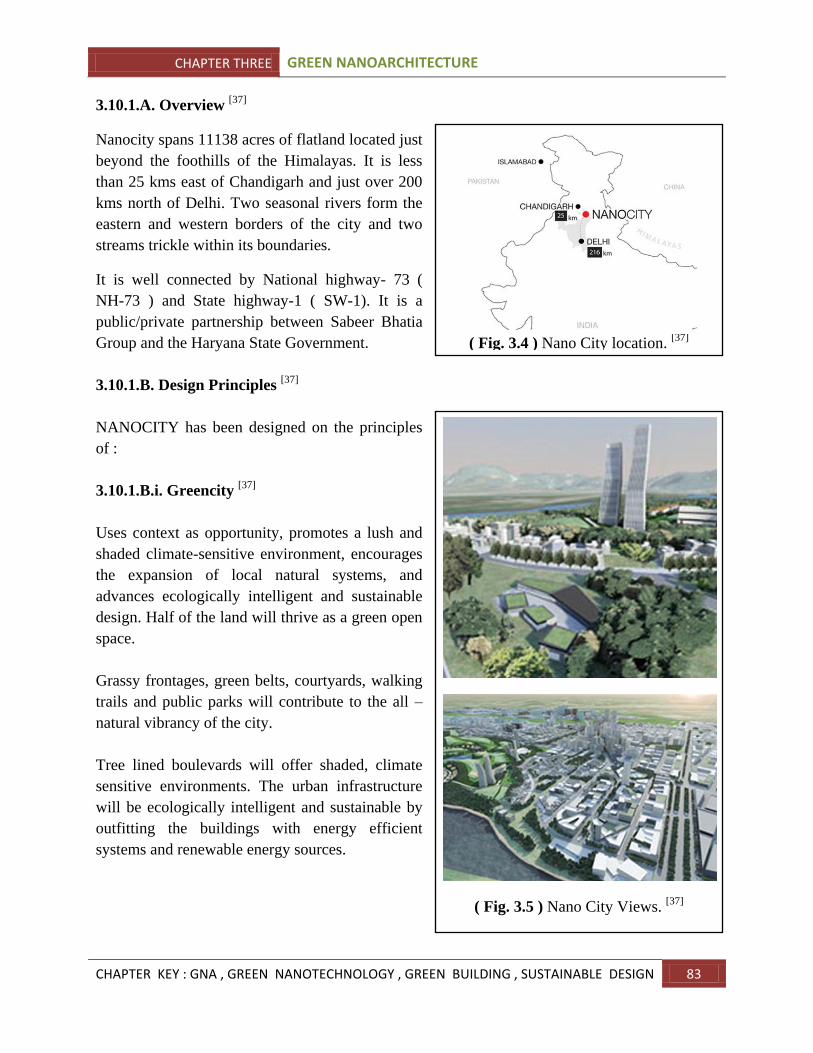
CHAPTER THREE GREEN NANOARCHITECTURE
CHAPTER KEY : GNA , GREEN NANOTECHNOLOGY , GREEN BUILDING , SUSTAINABLE DESIGN 83
3.10.1.A. Overview [37]
Nanocity spans 11138 acres of flatland located just
beyond the foothills of the Himalayas. It is less
than 25 kms east of Chandigarh and just over 200
kms north of Delhi. Two seasonal rivers form the
eastern and western borders of the city and two
streams trickle within its boundaries.
It is well connected by National highway- 73 (
NH-73 ) and State highway-1 ( SW-1). It is a
public/private partnership between Sabeer Bhatia
Group and the Haryana State Government.
3.10.1.B. Design Principles [37]
NANOCITY has been designed on the principles
of :
3.10.1.B.i. Greencity [37]
Uses context as opportunity, promotes a lush and
shaded climate-sensitive environment, encourages
the expansion of local natural systems, and
advances ecologically intelligent and sustainable
design. Half of the land will thrive as a green open
space.
Grassy frontages, green belts, courtyards, walking
trails and public parks will contribute to the all –
natural vibrancy of the city.
Tree lined boulevards will offer shaded, climate
sensitive environments. The urban infrastructure
will be ecologically intelligent and sustainable by
outfitting the buildings with energy efficient
systems and renewable energy sources.
( Fig. 3.4 ) Nano City location. [37]
( Fig. 3.5 ) Nano City Views. [37]
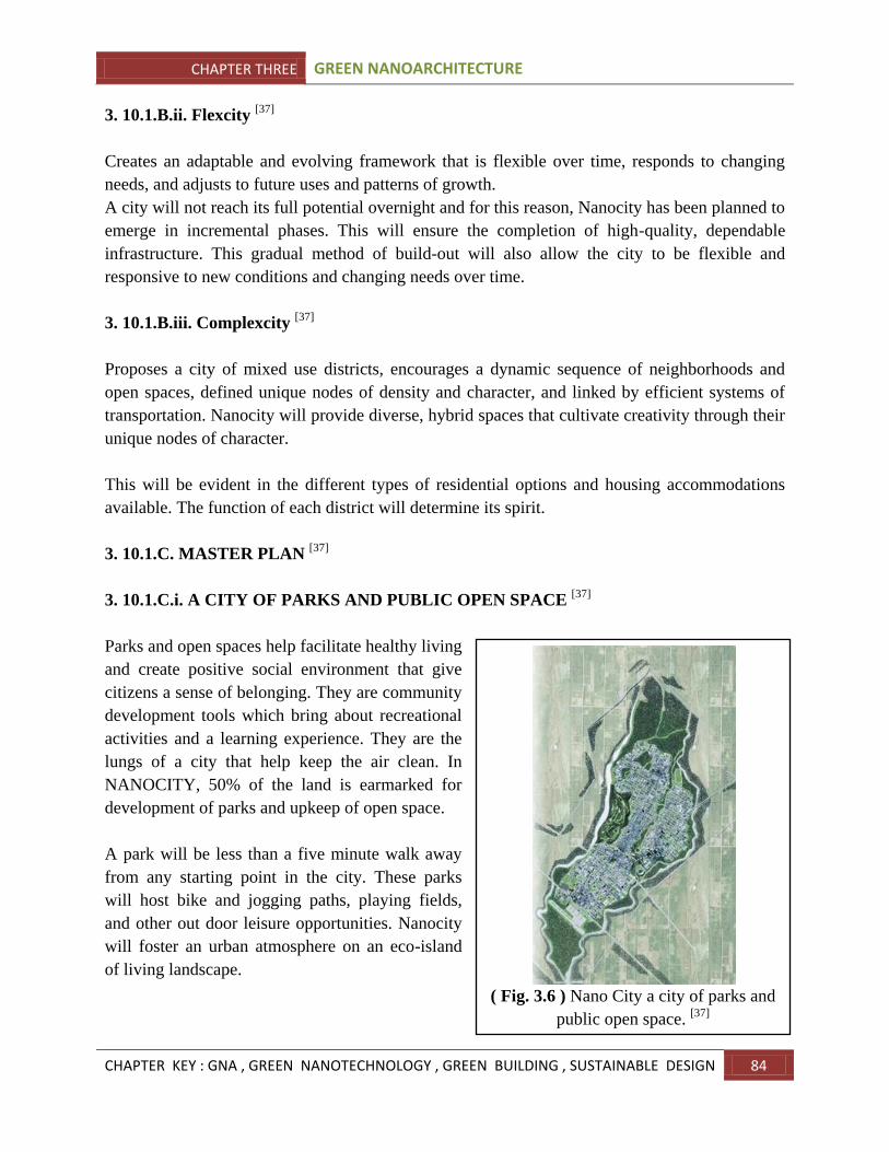
CHAPTER THREE GREEN NANOARCHITECTURE
CHAPTER KEY : GNA , GREEN NANOTECHNOLOGY , GREEN BUILDING , SUSTAINABLE DESIGN 84
3. 10.1.B.ii. Flexcity [37]
Creates an adaptable and evolving framework that is flexible over time, responds to changing
needs, and adjusts to future uses and patterns of growth.
A city will not reach its full potential overnight and for this reason, Nanocity has been planned to
emerge in incremental phases. This will ensure the completion of high-quality, dependable
infrastructure. This gradual method of build-out will also allow the city to be flexible and
responsive to new conditions and changing needs over time.
3. 10.1.B.iii. Complexcity [37]
Proposes a city of mixed use districts, encourages a dynamic sequence of neighborhoods and
open spaces, defined unique nodes of density and character, and linked by efficient systems of
transportation. Nanocity will provide diverse, hybrid spaces that cultivate creativity through their
unique nodes of character.
This will be evident in the different types of residential options and housing accommodations
available. The function of each district will determine its spirit.
3. 10.1.C. MASTER PLAN [37]
3. 10.1.C.i. A CITY OF PARKS AND PUBLIC OPEN SPACE [37]
Parks and open spaces help facilitate healthy living
and create positive social environment that give
citizens a sense of belonging. They are community
development tools which bring about recreational
activities and a learning experience. They are the
lungs of a city that help keep the air clean. In
NANOCITY, 50% of the land is earmarked for
development of parks and upkeep of open space.
A park will be less than a five minute walk away
from any starting point in the city. These parks
will host bike and jogging paths, playing fields,
and other out door leisure opportunities. Nanocity
will foster an urban atmosphere on an eco-island
of living landscape.
( Fig. 3.6 ) Nano City a city of parks and
public open space. [37]
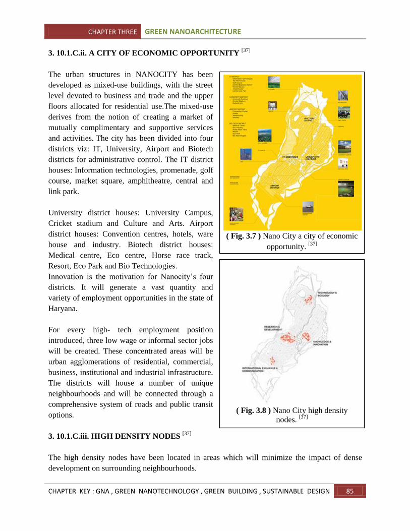
CHAPTER THREE GREEN NANOARCHITECTURE
CHAPTER KEY : GNA , GREEN NANOTECHNOLOGY , GREEN BUILDING , SUSTAINABLE DESIGN 85
3. 10.1.C.ii. A CITY OF ECONOMIC OPPORTUNITY [37]
The urban structures in NANOCITY has been
developed as mixed-use buildings, with the street
level devoted to business and trade and the upper
floors allocated for residential use.The mixed-use
derives from the notion of creating a market of
mutually complimentary and supportive services
and activities. The city has been divided into four
districts viz: IT, University, Airport and Biotech
districts for administrative control. The IT district
houses: Information technologies, promenade, golf
course, market square, amphitheatre, central and
link park.
University district houses: University Campus,
Cricket stadium and Culture and Arts. Airport
district houses: Convention centres, hotels, ware
house and industry. Biotech district houses:
Medical centre, Eco centre, Horse race track,
Resort, Eco Park and Bio Technologies.
Innovation is the motivation for Nanocity‟s four
districts. It will generate a vast quantity and
variety of employment opportunities in the state of
Haryana.
For every high- tech employment position
introduced, three low wage or informal sector jobs
will be created. These concentrated areas will be
urban agglomerations of residential, commercial,
business, institutional and industrial infrastructure.
The districts will house a number of unique
neighbourhoods and will be connected through a
comprehensive system of roads and public transit
options.
3. 10.1.C.iii. HIGH DENSITY NODES [37]
The high density nodes have been located in areas which will minimize the impact of dense
development on surrounding neighbourhoods.
( Fig. 3.7 ) Nano City a city of economic
opportunity. [37]
( Fig. 3.8 ) Nano City high density
nodes. [37]
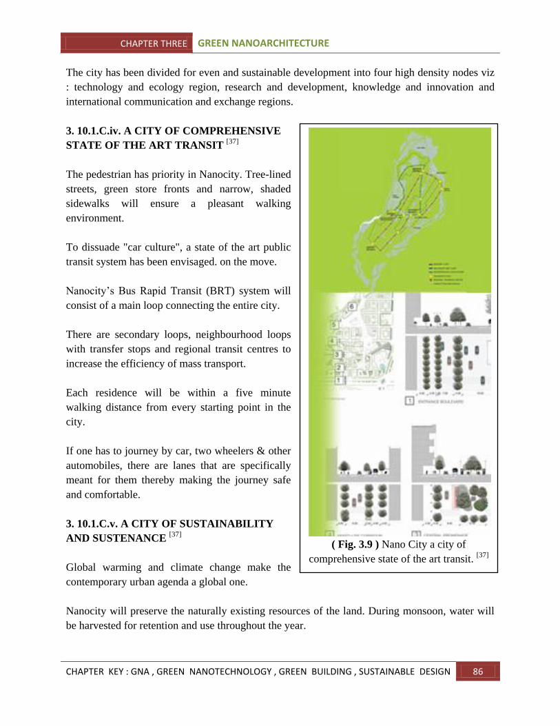
CHAPTER THREE GREEN NANOARCHITECTURE
CHAPTER KEY : GNA , GREEN NANOTECHNOLOGY , GREEN BUILDING , SUSTAINABLE DESIGN 86
The city has been divided for even and sustainable development into four high density nodes viz
: technology and ecology region, research and development, knowledge and innovation and
international communication and exchange regions.
3. 10.1.C.iv. A CITY OF COMPREHENSIVE
STATE OF THE ART TRANSIT [37]
The pedestrian has priority in Nanocity. Tree-lined
streets, green store fronts and narrow, shaded
sidewalks will ensure a pleasant walking
environment.
To dissuade "car culture", a state of the art public
transit system has been envisaged. on the move.
Nanocity‟s Bus Rapid Transit (BRT) system will
consist of a main loop connecting the entire city.
There are secondary loops, neighbourhood loops
with transfer stops and regional transit centres to
increase the efficiency of mass transport.
Each residence will be within a five minute
walking distance from every starting point in the
city.
If one has to journey by car, two wheelers & other
automobiles, there are lanes that are specifically
meant for them thereby making the journey safe
and comfortable.
3. 10.1.C.v. A CITY OF SUSTAINABILITY
AND SUSTENANCE [37]
Global warming and climate change make the
contemporary urban agenda a global one.
Nanocity will preserve the naturally existing resources of the land. During monsoon, water will
be harvested for retention and use throughout the year.
( Fig. 3.9 ) Nano City a city of
comprehensive state of the art transit. [37]
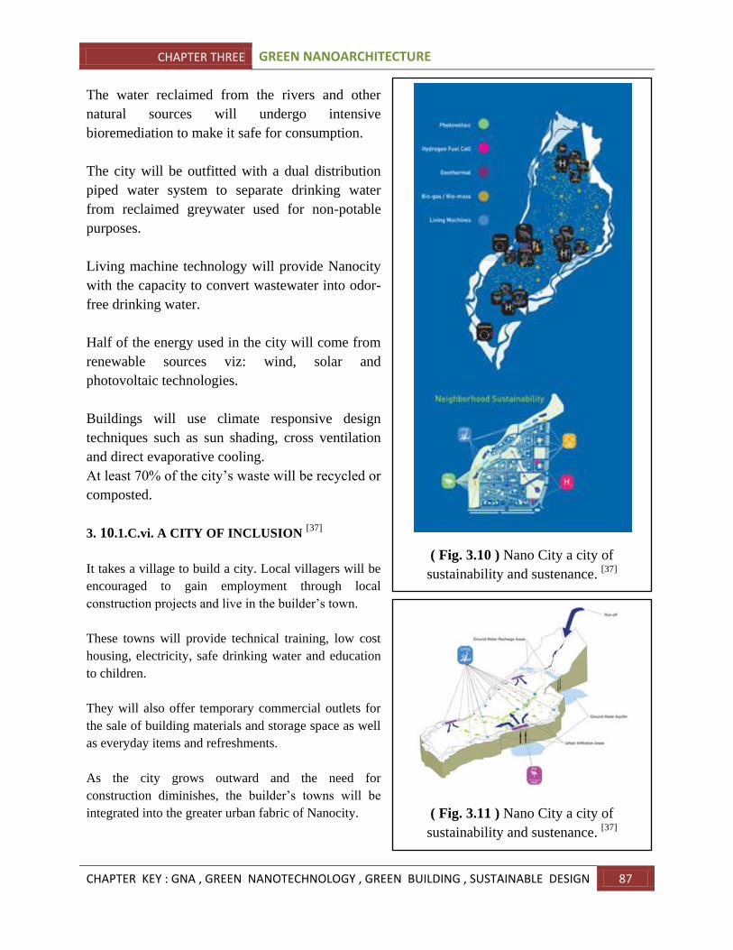
CHAPTER THREE GREEN NANOARCHITECTURE
CHAPTER KEY : GNA , GREEN NANOTECHNOLOGY , GREEN BUILDING , SUSTAINABLE DESIGN 87
The water reclaimed from the rivers and other
natural sources will undergo intensive
bioremediation to make it safe for consumption.
The city will be outfitted with a dual distribution
piped water system to separate drinking water
from reclaimed greywater used for non-potable
purposes.
Living machine technology will provide Nanocity
with the capacity to convert wastewater into odor-
free drinking water.
Half of the energy used in the city will come from
renewable sources viz: wind, solar and
photovoltaic technologies.
Buildings will use climate responsive design
techniques such as sun shading, cross ventilation
and direct evaporative cooling.
At least 70% of the city‟s waste will be recycled or
composted.
3. 10.1.C.vi. A CITY OF INCLUSION [37]
It takes a village to build a city. Local villagers will be
encouraged to gain employment through local
construction projects and live in the builder‟s town.
These towns will provide technical training, low cost
housing, electricity, safe drinking water and education
to children.
They will also offer temporary commercial outlets for
the sale of building materials and storage space as well
as everyday items and refreshments.
As the city grows outward and the need for
construction diminishes, the builder‟s towns will be
integrated into the greater urban fabric of Nanocity.
( Fig. 3.10 ) Nano City a city of
sustainability and sustenance. [37]
( Fig. 3.11 ) Nano City a city of
sustainability and sustenance. [37]
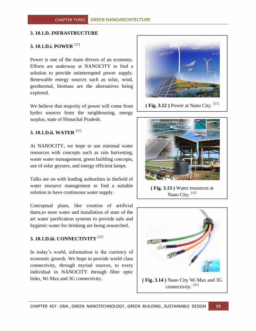
CHAPTER THREE GREEN NANOARCHITECTURE
CHAPTER KEY : GNA , GREEN NANOTECHNOLOGY , GREEN BUILDING , SUSTAINABLE DESIGN 88
3. 10.1.D. INFRASTRUCTURE
3. 10.1.D.i. POWER [37]
Power is one of the main drivers of an economy.
Efforts are underway at NANOCITY to find a
solution to provide uninterrupted power supply.
Renewable energy sources such as solar, wind,
geothermal, biomass are the alternatives being
explored.
We believe that majority of power will come from
hydro sources from the neighbouring, energy
surplus, state of Himachal Pradesh.
3. 10.1.D.ii. WATER [37]
At NANOCITY, we hope to use minimal water
resources with concepts such as rain harvesting,
waste water management, green building concepts,
use of solar geysers, and energy efficient lamps.
Talks are on with leading authorities in thefield of
water resource management to find a suitable
solution to have continuous water supply.
Conceptual plans, like creation of artificial
dams,to store water and installation of state of the
art water purification systems to provide safe and
hygienic water for drinking are being researched.
3. 10.1.D.iii. CONNECTIVITY [37]
In today‟s world, information is the currency of
economic growth. We hope to provide world class
connectivity, through myriad sources, to every
individual in NANOCITY through fibre optic
links, Wi Max and 3G connectivity.
( Fig. 3.12 ) Power at Nano City. [37]
( Fig. 3.13 ) Water resources at
Nano City. [37]
( Fig. 3.14 ) Nano City Wi Max and 3G
connectivity. [37]
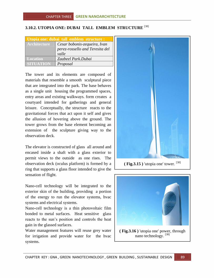
CHAPTER THREE GREEN NANOARCHITECTURE
CHAPTER KEY : GNA , GREEN NANOTECHNOLOGY , GREEN BUILDING , SUSTAINABLE DESIGN 89
3.10.2. UTOPIA ONE: DUBAI TALL EMBLEM STRUCTURE [38]
Utopia one: dubai tall emblem structure :
Architecture Cesar bobonis-zequeira, Ivan
perez-rossello and Teresita del
valle
Location Zaabeel Park.Dubai
SITUATION Proposal
The tower and its elements are composed of
materials that resemble a smooth sculptural piece
that are integrated into the park. The base behaves
as a single unit housing the programmed spaces,
entry areas and existing walkways. form creates a
courtyard intended for gatherings and general
leisure. Conceptually, the structure reacts to the
gravitational forces that act upon it self and gives
the allusion of hovering above the ground. The
tower grows from the base element becoming an
extension of the sculpture giving way to the
observation deck.
The elevator is constructed of glass all around and
encased inside a shaft with a glass exterior to
permit views to the outside as one rises. The
observation deck (oculus platform) is formed by a
ring that supports a glass floor intended to give the
sensation of flight.
Nano-cell technology will be integrated to the
exterior skin of the building, providing a portion
of the energy to run the elevator systems, hvac
systems and electrical systems.
Nano-cell technology is a thin photovoltaic film
bonded to metal surfaces. Heat sensitive glass
reacts to the sun‟s position and controls the heat
gain in the glassed surfaces.
Water management features will reuse grey water
for irrigation and provide water for the hvac
systems.
( Fig.3.15 ) 'utopia one' tower. [38]
( Fig.3.16 ) 'utopia one' power, through
nano technology. [38]
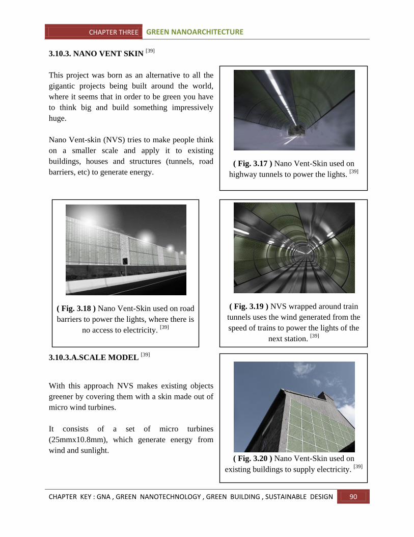
CHAPTER THREE GREEN NANOARCHITECTURE
CHAPTER KEY : GNA , GREEN NANOTECHNOLOGY , GREEN BUILDING , SUSTAINABLE DESIGN 90
3.10.3. NANO VENT SKIN [39]
This project was born as an alternative to all the
gigantic projects being built around the world,
where it seems that in order to be green you have
to think big and build something impressively
huge.
Nano Vent-skin (NVS) tries to make people think
on a smaller scale and apply it to existing
buildings, houses and structures (tunnels, road
barriers, etc) to generate energy.
3.10.3.A.SCALE MODEL [39]
With this approach NVS makes existing objects
greener by covering them with a skin made out of
micro wind turbines.
It consists of a set of micro turbines
(25mmx10.8mm), which generate energy from
wind and sunlight.
( Fig. 3.17 ) Nano Vent-Skin used on
highway tunnels to power the lights. [39]
( Fig. 3.20 ) Nano Vent-Skin used on
existing buildings to supply electricity. [39]
( Fig. 3.19 ) NVS wrapped around train
tunnels uses the wind generated from the
speed of trains to power the lights of the
next station. [39]
( Fig. 3.18 ) Nano Vent-Skin used on road
barriers to power the lights, where there is
no access to electricity. [39]
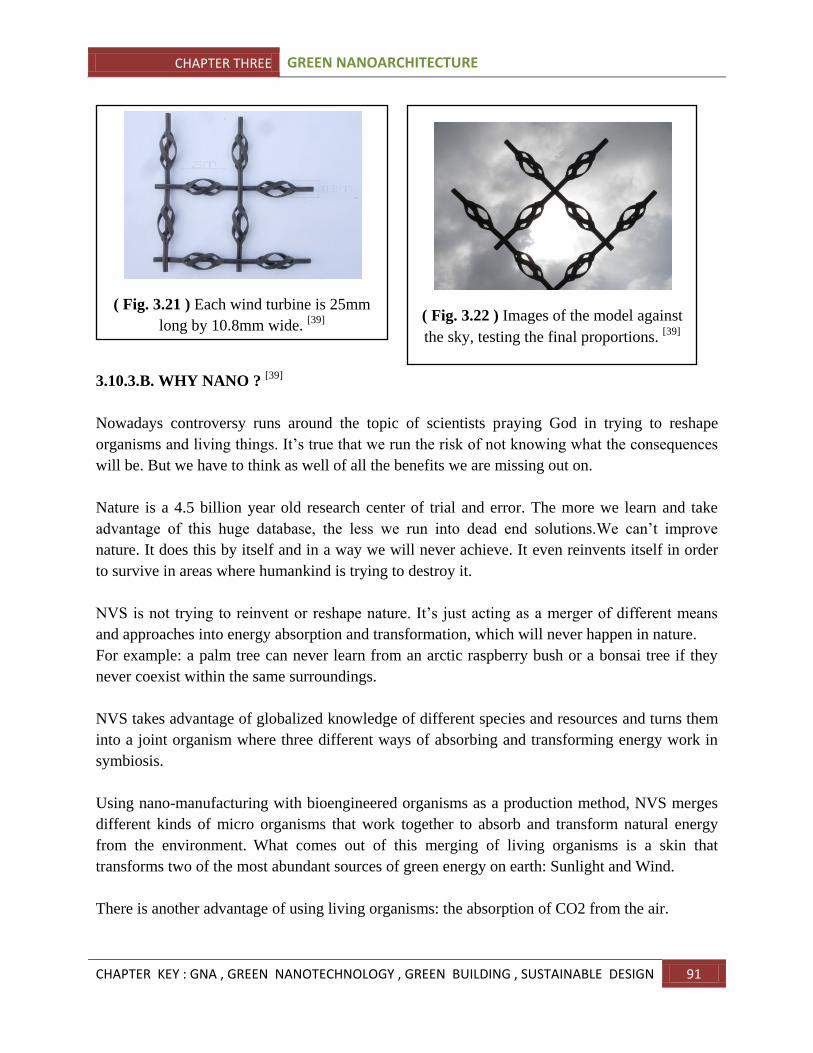
CHAPTER THREE GREEN NANOARCHITECTURE
CHAPTER KEY : GNA , GREEN NANOTECHNOLOGY , GREEN BUILDING , SUSTAINABLE DESIGN 91
3.10.3.B. WHY NANO ? [39]
Nowadays controversy runs around the topic of scientists praying God in trying to reshape
organisms and living things. It‟s true that we run the risk of not knowing what the consequences
will be. But we have to think as well of all the benefits we are missing out on.
Nature is a 4.5 billion year old research center of trial and error. The more we learn and take
advantage of this huge database, the less we run into dead end solutions.We can‟t improve
nature. It does this by itself and in a way we will never achieve. It even reinvents itself in order
to survive in areas where humankind is trying to destroy it.
NVS is not trying to reinvent or reshape nature. It‟s just acting as a merger of different means
and approaches into energy absorption and transformation, which will never happen in nature.
For example: a palm tree can never learn from an arctic raspberry bush or a bonsai tree if they
never coexist within the same surroundings.
NVS takes advantage of globalized knowledge of different species and resources and turns them
into a joint organism where three different ways of absorbing and transforming energy work in
symbiosis.
Using nano-manufacturing with bioengineered organisms as a production method, NVS merges
different kinds of micro organisms that work together to absorb and transform natural energy
from the environment. What comes out of this merging of living organisms is a skin that
transforms two of the most abundant sources of green energy on earth: Sunlight and Wind.
There is another advantage of using living organisms: the absorption of CO2 from the air.
( Fig. 3.21 ) Each wind turbine is 25mm
long by 10.8mm wide. [39]
( Fig. 3.22 ) Images of the model against
the sky, testing the final proportions. [39]
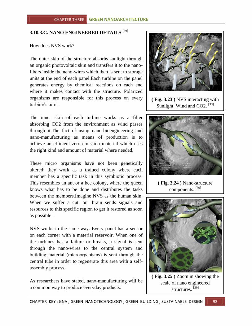
CHAPTER THREE GREEN NANOARCHITECTURE
CHAPTER KEY : GNA , GREEN NANOTECHNOLOGY , GREEN BUILDING , SUSTAINABLE DESIGN 92
3.10.3.C. NANO ENGINEERED DETAILS [39]
How does NVS work?
The outer skin of the structure absorbs sunlight through
an organic photovoltaic skin and transfers it to the nano-
fibers inside the nano-wires which then is sent to storage
units at the end of each panel.Each turbine on the panel
generates energy by chemical reactions on each end
where it makes contact with the structure. Polarized
organisms are responsible for this process on every
turbine‟s turn.
The inner skin of each turbine works as a filter
absorbing CO2 from the environment as wind passes
through it.The fact of using nano-bioengineering and
nano-manufacturing as means of production is to
achieve an efficient zero emission material which uses
the right kind and amount of material where needed.
These micro organisms have not been genetically
altered; they work as a trained colony where each
member has a specific task in this symbiotic process.
This resembles an ant or a bee colony, where the queen
knows what has to be done and distributes the tasks
between the members.Imagine NVS as the human skin.
When we suffer a cut, our brain sends signals and
resources to this specific region to get it restored as soon
as possible.
NVS works in the same way. Every panel has a sensor
on each corner with a material reservoir. When one of
the turbines has a failure or breaks, a signal is sent
through the nano-wires to the central system and
building material (microorganisms) is sent through the
central tube in order to regenerate this area with a self-
assembly process.
As researchers have stated, nano-manufacturing will be
a common way to produce everyday products.
( Fig. 3.23 ) NVS interacting with
Sunlight, Wind and CO2. [39]
( Fig. 3.24 ) Nano-structure
components. [39]
( Fig. 3.25 ) Zoom in showing the
scale of nano engineered
structures. [39]
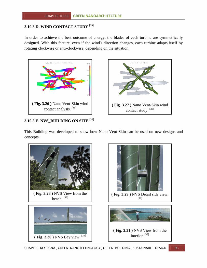
CHAPTER THREE GREEN NANOARCHITECTURE
CHAPTER KEY : GNA , GREEN NANOTECHNOLOGY , GREEN BUILDING , SUSTAINABLE DESIGN 93
3.10.3.D. WIND CONTACT STUDY [39]
In order to achieve the best outcome of energy, the blades of each turbine are symmetrically
designed. With this feature, even if the wind's direction changes, each turbine adapts itself by
rotating clockwise or anti-clockwise, depending on the situation.
3.10.3.E. NVS_BUILDING ON SITE [39]
This Building was developed to show how Nano Vent-Skin can be used on new designs and
concepts.
( Fig. 3.27 ) Nano Vent-Skin wind
contact study. [39]
( Fig. 3.26 ) Nano Vent-Skin wind
contact analysis. [39]
( Fig. 3.28 ) NVS View from the
beach. [39]
( Fig. 3.29 ) NVS Detail side view. [39]
( Fig. 3.30 ) NVS Bay view. [39]
( Fig. 3.31 ) NVS View from the
interior. [39]
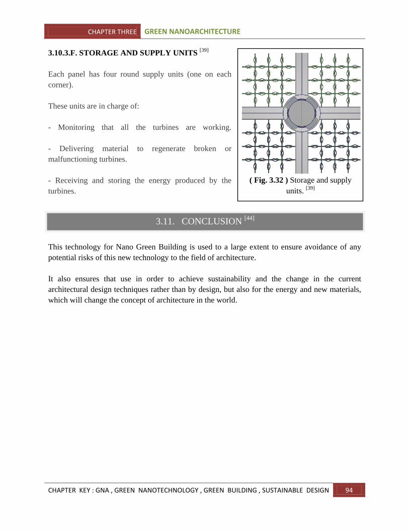
CHAPTER THREE GREEN NANOARCHITECTURE
CHAPTER KEY : GNA , GREEN NANOTECHNOLOGY , GREEN BUILDING , SUSTAINABLE DESIGN 94
3.10.3.F. STORAGE AND SUPPLY UNITS [39]
Each panel has four round supply units (one on each
corner).
These units are in charge of:
- Monitoring that all the turbines are working.
- Delivering material to regenerate broken or
malfunctioning turbines.
- Receiving and storing the energy produced by the
turbines.
This technology for Nano Green Building is used to a large extent to ensure avoidance of any
potential risks of this new technology to the field of architecture.
It also ensures that use in order to achieve sustainability and the change in the current
architectural design techniques rather than by design, but also for the energy and new materials,
which will change the concept of architecture in the world.
( Fig. 3.32 ) Storage and supply
units. [39]
3.11. CONCLUSION [44]
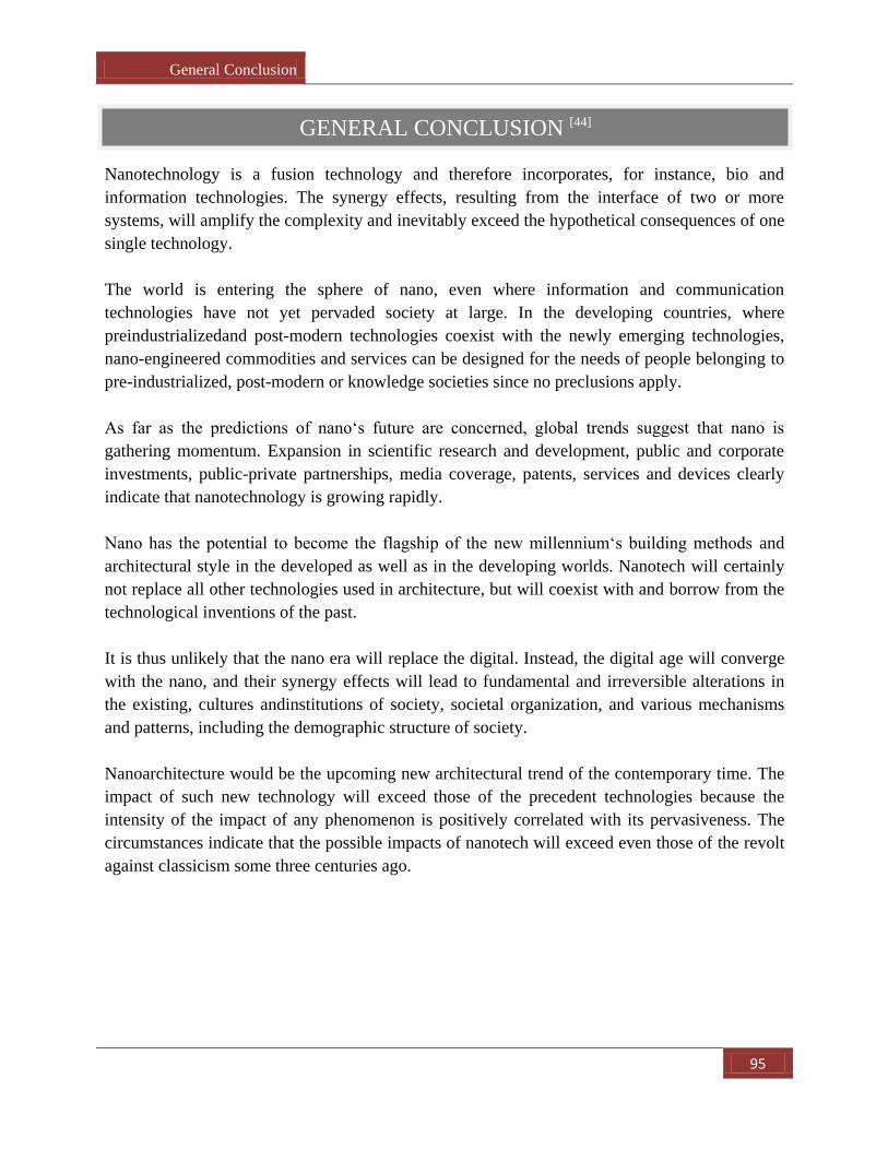
General Conclusion
95
Nanotechnology is a fusion technology and therefore incorporates, for instance, bio and
information technologies. The synergy effects, resulting from the interface of two or more
systems, will amplify the complexity and inevitably exceed the hypothetical consequences of one
single technology.
The world is entering the sphere of nano, even where information and communication
technologies have not yet pervaded society at large. In the developing countries, where
preindustrializedand post-modern technologies coexist with the newly emerging technologies,
nano-engineered commodities and services can be designed for the needs of people belonging to
pre-industrialized, post-modern or knowledge societies since no preclusions apply.
As far as the predictions of nano‘s future are concerned, global trends suggest that nano is
gathering momentum. Expansion in scientific research and development, public and corporate
investments, public-private partnerships, media coverage, patents, services and devices clearly
indicate that nanotechnology is growing rapidly.
Nano has the potential to become the flagship of the new millennium‘s building methods and
architectural style in the developed as well as in the developing worlds. Nanotech will certainly
not replace all other technologies used in architecture, but will coexist with and borrow from the
technological inventions of the past.
It is thus unlikely that the nano era will replace the digital. Instead, the digital age will converge
with the nano, and their synergy effects will lead to fundamental and irreversible alterations in
the existing, cultures andinstitutions of society, societal organization, and various mechanisms
and patterns, including the demographic structure of society.
Nanoarchitecture would be the upcoming new architectural trend of the contemporary time. The
impact of such new technology will exceed those of the precedent technologies because the
intensity of the impact of any phenomenon is positively correlated with its pervasiveness. The
circumstances indicate that the possible impacts of nanotech will exceed even those of the revolt
against classicism some three centuries ago.
GENERAL CONCLUSION [44]
References
96
Textbooks:
(1) Digital Architecture Now: A Global Survey of Emerging Talent by Neil Spiller , (2008) .
(2) Nano Materials in architecture, Interior architecture and Design. Leydecker, Sylvia.
(2008).
EBooks:
(3) Government Investment in Nanotechnology Fifth Report of Session 2003 , 04 Report
Volume I Ordered by The House of Commons . http://www.publications.parliament.uk/ .
Retrieved July, 2009.
(4) Nano material science . Nanotechnology : A Brief Introduction , Luisa filipponi & Duncan
Stherland Interdisciplinary Nanoscience center (INANO) University of Aarhus, Denmark
http://www.nanocap.eu/Flex/Site/Download.aspx?ID=2256 . Retrieved March, 2009.
(5) Sustainable Architecture Module: Qualities, Use, and Examples of Sustainable
Building Materials Written by Jong-Jin Kim, Assistant Professor of Architecture,
and Brenda Rigdon, Project Intern; Edited by Jonathan Graves, Project Intern College of
Architecture and Urban Planning The University of Michigan . Retrieved July, 2009.
(6) Nano The Essentials: Understanding Nanoscience and Technology. Pradeep, T.
McGrew Hill, New Delhi, (2007). . Retrieved May, 2009.
Web articles:
(7) Nanotechnology provides 'green' path to environmentally sustainable economy .
Posted April 26th, 2007 http://www.physorg.com/news96781160.html . Retrieved March,
2009.
(8) NT Introduction http://www.etcgroup.org/ . Retrieved November, 2008.
(9) Nano for Science and Engineering. http://en.wikipedia.org/wiki/Nano. Retrieved October,2008.
(10) Nano Scale . http://www.discovernano.northwestern.edu/whatis/index_html/howsmall_html .
Retrieved October, 2009.
(11) Definition of Nanoscience . http://www.discovernano.northwestern.edu/whatis/index_
html/sizematters_html . Retrieved November, 2008.
(12) Nanotechnology . http://en.wikipedia.org/wiki/Nanotechnology . Retrieved October, 2008.
(13) What’s Nanotechnology. http://www.nano.org.uk/whatis.htm. Retrieved August, 2009.
(14) http://1nanotechnology.blogspot.com/2007/08/conclusion.html . Retrieved May, 2009.
(15) Nanoarchitecture Introduction . Yeadon, Peter. Year 2050: Cities in the Age of
Nanotechnology , http://sensingarchitecture.com/523/nanotechnology-and-new-materials-for-architecture/
Retrieved April, 2009.
REFERENCES
References
97
(16) Digital architecture . http://architecture-now2.blogspot.com/2008/07/artspacearchitecture-and-
landscape.html , Posted July 21, 2008 . Retrieved May, 2009.
(17) Digitally Grown Botanic Tower http://aminima.net/wp/?p=840&language=en . Retrieved
May, 2009.
(18) A Science Impacting Architectural Design . Elvin, Dr. George. NanoBioBuilding:
Nanotechnology, Biotechnology, and the Future of Building. Green Technology Forum.
2006 , http://sensingarchitecture.com/2009/02/11/nanotechnology-a-science-impacting-architectural-design/
Retrieved March, 2009.
(19) Nano Studio, Filed in archive Design by George Elvin on November 29, 2006
http://www.nanotechbuzz.com/50226711/nanostudio_explores_architecture_and_nanotechnology.php .
Retrieved January, 2009.
(20) GNA Introduction . http://www.azonano.com/news.asp?newsID=2129 . Retrieved
February, 2009.
(21) Green Nanotechnology . http://en.wikipedia.org/wiki/Green_nanotechnology . Retrieved
January, 2009.
(22) Evaluation of 'Green' Nanotechnology requires a Full Life Cycle Assessment.
Posted: February 23, 2009 http://www.nanowerk.com/spotlight/spotid=9386.php . Retrieved
March, 2009.
(23) Nanotechnology and Sustainability , Posted 22 Jun, 2007
http://www.scitizen.com/screens/blogPage/viewBlog/sw_viewBlog.php?idTheme=5&idContribution=750
Retrieved December, 2008.
Websites:
(24) Definition of Nano http://www.discovernano.northwestern.edu/whatis/index_html/index_html .
Retrieved October, 2008.
(25) Carbon Nanotube http://www.cnano-rhone-alpes.org/spip.php?article57 . Retrieved June, 2009.
(26) Image of Nanowires http://library.thinkquest.org/05aug/01179/nanowires.html . Retrieved May,
2009.
(27) Image of C60/fullerenes
http://www.nanowerk.com/nanotechnology/introduction/introduction_to_nanotechnology_11.html .
Retrieved May, 2009.
(28) Image of Geodesic Domes by C60/ fullerenes www.answers.com/topic/r-buckminster-fuller .
Retrieved May, 2009.
(29) Image of Nanoparticle . http://library.thinkquest.org/07aug/02147/particlegeneral.html . Retrieved
July, 2009.
(30) Nanotechnology Applications . http://understandingnano.com/ . Retrieved August, 2009.
(31) Nanotechnology's Potential to Reduce Greenhouse Gases .
http://www.nanowerk.com/spotlight/spotid=2225.php . Retrieved July, 2009.
References
98
(32) Definition of Nanoarchitecture . http://www2.arch.uiuc.edu/elvin/nanotech.htm Retrieved
January, 2009.
(33) Future of the Built Environment . http://www2.arch.uiuc.edu/elvin/smallplans.htm Retrieved
March, 2009.
(34) Nanoarchitecture Application .
http://greendimensions.wikidot.com/nanotechnology-in-architecture . Retrieved April, 2009.
(35) Next Generation Building Cleaning Solution . http://www.edgecryojetics.com/pages/self-
cleaning.html . Retrieved July, 2009.
(36) The Nano Towers . http://www.archicentral.com/the-nano-towers-by-allard-architecture-17754/ .
Retrieved August, 2009.
(37) Nano City . http://www.nanocity.com/index.html . Retrieved February 2009.
(38) Utopia One: Dubai Tall Emblem Structure .
http://www.designboom.com/weblog/cat/9/view/6490/utopia-one-dubai-tall-emblem-structure.html .
Retrieved august 2009.
(39) Nano Vent-skin . http://nanoventskin.blogspot.com/ . Retrieved December , 2008.
Periodical:
(40) EPA And Nanotechnology: Oversight for the 21st Century , J. Clarence Davies PEN 9
MAY 2007 http://www.nanotechproject.org/file_download/files/Nano&EPA_PEN9.pdf . Retrieved
April , 2009.
(41) Nanotechnology and Developing Countries Part 2: What Realities?
http://www.azonano.com/details.asp?ArticleID=1429 . Retrieved August, 2009.
(42) Nanotechnologies in the 21st Century : Challenges and Opportunities
to Green Nanotechnologies Issue 1. april 2009 . Retrieved May, 2009.
(43) Principles of Green Engineering . Green Nanotechnology: It's Easier Than You Think -
Project on Emerging Technologies, USA . Retrieved February, 2009.
(44) The Author.

الرسالة ملخص
99
هذه الرسالة تلقى الضوء على التطور المالحظ فى اآلونة اآلخيرة فى استكشاف الجديد فى مجال التكنولوجيا والذى ادى
اليومية بداية من أجهزة الحاسوب صغيرة الحجم وفائقة السرعة الى ظهور تكنولوجيا النانو حيث أصبحت ترتبط بحياتنا واألقمشة المقاومة للبقع وحتى عالج المرضى من خاليا سرطانية معينة وقد أصبح العديد من المنتجات المطروحة باالسواق
تغالل األمثل للتكنولوجيا والجدير بالذآر أن معظم هذه المنتجات تعتمد على األس .تعتمد فى صناعتها على تكنولوجيا النانوومن المتوقع أن تشهد العقود المقبلة طفرة هائلة فى هذه .المتعارف عليها مثل األسطح المقاومة للخدش او التصاق األتربة بها
.التكنولوجيا ستدهش البشرية جمعاءلة بدءا من تعريف تكنولوجيا تم تقسيم هذه الرسالة الى ثالثة أجزاء يتم من خاللها عرض الموضوع بطريقة علمية متسلس
.النانو وما قدمته تلك التكنولوجيا للبشرية وأثرها فى مجال العمارة وآذلك على فكر المهندس المعمارى فى وقتنا هذا :ونلخصها فيما يلى
تكنولوجيا النانو -١
والجديد مما يساعد على حياة افضل آنتيجة متوقعة للبحث العلمى والتطور المستمر فى مجال التكنولوجيا يتم اآتشاف الكثيرللبشرية ومن هذا المنطلق يبدأ حديثنا فى الباب األول عن تعريف لمعنى آلمة نانو ومن ثم نتجه الى المقاييس المتناهية فى
حيث اآتشاف هذه الجزيئات المتناهية فى الصغر أدى الى NANO SCALE )(الصغر التى تقاس بوحدة النانو متر وقد أخترقت هذه التكنولوجيا .وبالتالى الى ظهور تكنولوجيا النانو NANO SCIENCE)(مى فى مجال النانو البحث العل
.جميع المجاالت فى الحياة وذلك يرجع الى الخصائص و المميزات الناتجة عنها عمارة النانو -٢
على هذا المجال من عدة اوجه و يتجه حديثنا فى عمارة النانو هى عباره عن أندماج تكنولوجيا النانو مع العماره و تأثيرها هذا الباب الى األثارالمترتبة على اآتشاف تكنولوجيا النانو وتاثيرها على مجال العمارة وايضا على فكر المهندس المعمارى
اساليب التفكير فتكنولوجيا النانو لها أثرها على خصائص المواد وايضا على الطاقة والذى أدى بدوره الى أختالف ملحوظ فى والتصميم المعمارى حيث يتم عرض هذه األختالفات وآذلك التساؤالت عن وجود آية مخاطر اوأثارجانبية لتكنولوجيا النانو تعود بالضرر على األنسان والبيئة مما يجعلنا نأخذ الحذر ويكون التطوير فى تكنولوجيا النانو على مجال العمارة تطويرا
.تدامةيساعد على وجود األس عمارة النانو الخضراء -٣
عمارة النانو الخضراء هى عباره عن اندماج تكنولوجيا النانو الخضراء مع العماره او يمكن ان ننظر لها من وجه اخر و هو حيث أدت المخاوف من تكنولوجيا النانو الى توخى الحذر من األضرار الجانبية اندماج تكنولوجيا النانو مع العماره الخضراء
على األنسان والبيئة ولذلك آان األتجاه واأللحاح على وجود االستدامة فى استخدام تكنولوجيا النانو فى مجال العمارة حتى . رها الجانبية على األنسان والبيئةتكون عمارة النانو الخضراء لضمان األستفادة من تكنولوجيا النانو وتجنب أثا
وبالفعل بدأ البحث فى هذا االتجاه والوصول الى نتائج مبشره لمستقبل افضل لمجال العماره و ظهرت تلك النتائج فى التصميم لمستخدمه جيث بدء ظهور مدن بأآملها تبني بهذه التكنولوجيا مثل مدينة النانو آما ظهر التأثير ايضا على المواد المعماريه ا
فى عمليه البناء و الديكور واخيرا التأثير على الطاقه و جاء هذا التأثير من حيث جعل المواد المستخدمه مجدده للطاقه او بمعنى ادق مولده للطاقه و بذلك يكون الوصول للهدف من تكنولوجيا النانو قد تحقق و لكنه تحقق مع وجود االستدامه فى
.مجال العماره لبل افضل المبانى و بذلك نضمن مستق
الهدف االساسى من هذه الرساله هو توضيح اهمية تكنولوجيا النانو على البشريه و على جميع مجاالت الحياه و نتجه بالترآيز . على تأثيرها فى مجال العماره لتظهر عمارة النانو و بالتعمق فى هذا االندماج نتمكن من التوصل الى عمارة النانو الخضراء
الرسالة ملخص

نانو الخضراءال ةعمار من ةمقدم
ةحميدأحمد عمر فهد عبد العزيز. مةعمارريوس وبکال االسکندرية ةجامع
ةللحصول علی درج
ةالمعماري ةماجيستير فی الهندسال
ةموافق :ةالرسال على الحكم و ةالمناقش لجنة
) مشرفًا رئيسيًا( إبراهيم العال عبد محمد /دآتور أستاذ ---------------------------- ةمعماريلا ةهندسلا قسم ، المتفرغ عمارةلا أستاذ
ةاألسكندري ةجامع ، ةهندسلا ليةآ
)عضوًا( محمد طارق الصياد /دآتور أستاذ ----------------------------ة معماريلا ةهندسلا قسم ،المتفرغ عمارةلا أستاذ
ةاألسكندري ةجامع ، ةهندسلا ليةآ
)عضوًا( ودىمحمد هشام سع /دآتور أستاذ ---------------------------- ةعمارلا قسم ، عمارةلا أستاذ
ةاألسكندري ةجامع ، الجميلةفنون لا ليةآو وآيل
أبتهال البسطويسى /دآتور أستاذ ---------------------------- ثوبحلا و يالعلا اتدراسلل ةيلكلا لوآي ةاألسكندري ةجامع ، ةهندسلا ليةآ

موافقة :الرسالة االشراف على لجنة
) مشرفًا رئيسيًا( إبراهيم العال عبد محمد /دآتور أستاذ ---------------------------- ةمعماريلا ةهندسلا قسم ، المتفرغ عمارةلا أستاذ
ةاألسكندري ةجامع ، ةهندسلا ليةآ
) مشرفًا( الرحمنأسامة محمود عبد /دآتور أستاذ ---------------------------- ة معماريلا ةهندسلا قسم ، عمارةلا أستاذ
ةاألسكندري ةجامع ،ة هندسلا ليةآ

االسکندرية ةجامع ةالهندس ةآلي
مقس ةاريمعمال ةالهندس
الخضراءنانو ال ةعمار مةقدم ةرسال
ملقس ةاإلسكندري ةعمجا – ةالهندس ةآلي – ةاريمعمال ةالهندس ةدرج على الحصول تتطلبام نمض
يراجستم فى العلوم ةيارمعمالالهندسة
من ةمقدم
ةفهد عبد العزيز أحمد عمر حميد. معمارةريوس وبکال االسکندرية ةجامع
٢٠١٠يناير


