

Harmonic Limiting Standardsand Power Factor Correction
Techniques
P. Tenti and G. Spiazzi
Department of Electronics and InformaticsUniversity of Padova
Via Gradenigo 6/a, 35131 Padova - ITALYPhone: +39-49-8277503 Fax: +39-49-8277599
e-mail:[email protected]

6th European Conference on Power Electronics and Applications - EPE '95
2
OUTLINE
- BASICS OF POWER FACTOR CORRECTION
- REVIEW OF HARMONIC STANDARDS
- BASICS OF SINGLE-PHASE PFC TOPOLOGIES ANDCONTROL
- CONTROL TECHNIQUES FOR SINGLE-PHASE PFC'S ANDCOMMERCIAL CONTROL IC'S
- INSULATED TOPOLOGIES
- TECHNIQUES FOR IMPROVING OUTPUT VOLTAGECONTROL SPEED
- BASICS OF SOFT-SWITCHING TECHNIQUES
- SMALL-SIGNAL MODELING
- SINGLE-PHASE APPLICATION EXAMPLES
6th European Conference on Power Electronics and Applications - EPE '95
3
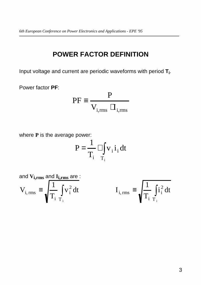
POWER FACTOR DEFINITION
Input voltage and current are periodic waveforms with period Ti.
Power factor PF:
rmsi,rmsi, IVP
PF⋅
≡
where P is the average power:
⋅=iT
iii
dtivT1
P
and Vi,rms and Ii,rms are :
≡iT
2i
irms i, dtv
T1
V ≡iT
2i
irms i, dti
T1
I

6th European Conference on Power Electronics and Applications - EPE '95
4
POWER FACTOR DEFINITION
Being voltage and current periodic waveforms we can write inFourier series:
( )∞
=φ+ω+=
1kkik0i ksinV2Vv
( )∞
=γ+ω+=
1kkik0i ksinI2Ii
V0 , I0 = average valuesVk , Ik = RMS values of harmonics
The average power is:
( )kkkk00 cosIVIVP γ−φ+=
CONSEQUENCE:
Current harmonic terms contributes to active power only in thepresence of voltage harmonic terms of the same frequency.
POWER FACTOR DEFINITION
0 ≤≤≤≤ PF ≤≤≤≤ 1

6th European Conference on Power Electronics and Applications - EPE '95
5
PF = 1 only if current and voltage are proportional
Power Factor Correction
An ideal Power Factor Corrector (PFC) takes from the supply acurrent which is proportional to the supply voltage
Rviem
i
i= emulated resistance
6th European Conference on Power Electronics and Applications - EPE '95
6
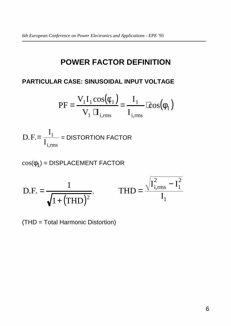
POWER FACTOR DEFINITION
PARTICULAR CASE: SINUSOIDAL INPUT VOLTAGE
( ) ( )1rmsi,
1
rms,i1
111 cosI
IIV
cosIVPF φ⋅=
⋅φ
=
D FI
I. .= l
i,rms = DISTORTION FACTOR
cos(φ1) = DISPLACEMENT FACTOR
( )2THD1
1.F.D
+= , THD
I II
i rms=−,
212
1
(THD = Total Harmonic Distortion)

6th European Conference on Power Electronics and Applications - EPE '95
7
POWER FACTOR REQUIREMENTS
PF = 1 implies:
o zero displacement between voltage and current fundamentalcomponent (φ1 = 0)
o zero current harmonic content
EXAMPLES:
cos(φ1) = 0, D.F. ≠ 0
cos(φ1) ≠ 0, D.F. = 0
In both cases PF<1

6th European Conference on Power Electronics and Applications - EPE '95
8
WHY POWER FACTOR CORRECTION
o Increased source efficiency- lower losses on source impedance- lower voltage distortion (cross-coupling)- higher power available from a given source
o Reduced low-frequency harmonic pollution
o Compliance with limiting standards (IEC 555-2, IEEE 519 etc.)

6th European Conference on Power Electronics and Applications - EPE '95
9
BASICS OF ACTIVE POWER FACTOR
CORRECTION

6th European Conference on Power Electronics and Applications - EPE '95
10
POWER FACTOR CORRECTION TECHNIQUES
PASSIVE METHODS: LC filters
o power factor not very high
o bulky components
o high reliability
o suitable for very small or high power levels
ACTIVE METHODS: high-frequency converters
o high power factor (approaching unity)
o possibility to introduce a high-frequency insulating transformer
o layout dependent high-frequency harmonics generation (EMIproblems)
o suitable for small and medium power levels

6th European Conference on Power Electronics and Applications - EPE '95
11
ACTIVE POWER FACTOR CORRECTION
DEFINITION:
Power Factor Corrector (PFC):AC/DC converter with sinusoidal current absorption(Current Proportional To Supply Voltage)
( )( ) t,senIi
senVv
iii
ii
ω=ϑϑ=ϑ=
The converter behaves like an equivalent resistance Rem given by:
R VIem
i
i=

6th European Conference on Power Electronics and Applications - EPE '95
12
ACTIVE POWER FACTOR CORRECTION:BASIC CONSIDERATIONS
Input power:( ) ( ) ( ) ( )
( )( )ϑ−==ϑ⋅=ϑ⋅ϑ=ϑ
2cos1IV sinIV2ivp
rms,irms,i
2rmsi,rmsi,iii
Considering unity efficiency:
V I P V Ii,rms i,rms⋅ = = ⋅
P = output power

6th European Conference on Power Electronics and Applications - EPE '95
13
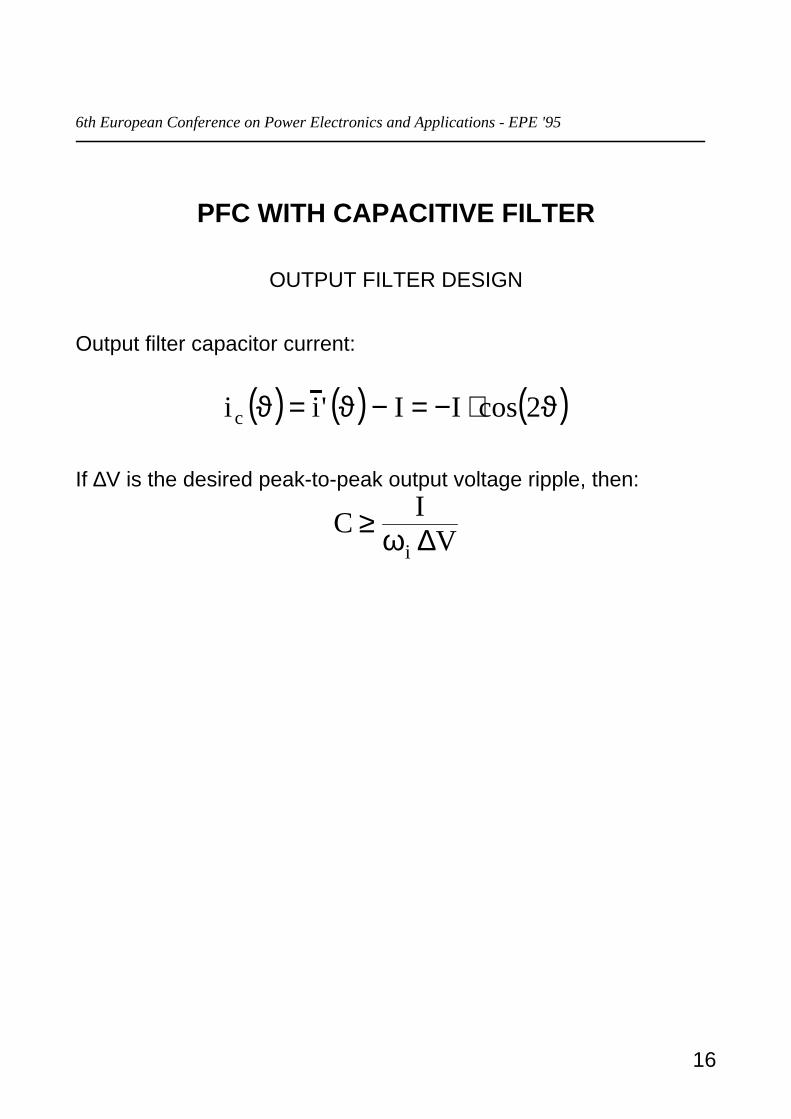
PFC WITH CAPACITIVE FILTER
ASSUMPTIONS:
o constant output voltage
o unity efficiency
o no low-frequency pulsating energy stored in the dc/dc stage
( ) ( )ϑ⋅=ϑ 'iVpi

6th European Conference on Power Electronics and Applications - EPE '95
14
PFC WITH CAPACITIVE FILTER
( ) ( ) ( )ϑ=ϑ
=ϑ′ 2i sinI2V
pi
( )ϑ'i = average value of ( )ϑ'i in a switching period
Voltage conversion ratio M':
( ) ( )( )( )ϑ′
ϑ=
ϑ=ϑ′
i
i
vV
M g
g
Load seen by the dc/dc stage:
( ) ( ) ( ) ( )( ) ( ) em
2
g
g2 RMi
vM
iV
R ⋅ϑ′=ϑ
ϑ⋅ϑ′=
ϑ′=ϑ′

6th European Conference on Power Electronics and Applications - EPE '95
15
PFC WITH CAPACITIVE FILTER
( ) ( )ϑ⋅=ϑ′
2sin2R
R
( ) ( ) gVVM,
sinMM =
ϑ=ϑ′
For a PFC we have:( )( ) em2
RMR
=ϑ′
ϑ′
a dc/dc converter when used as rectifier operates as a PFC withconstant control if : ( ) ( )ϑ′∝ϑ′ RM
6th European Conference on Power Electronics and Applications - EPE '95
16
PFC WITH CAPACITIVE FILTER
OUTPUT FILTER DESIGN
Output filter capacitor current:
( ) ( ) ( )ϑ⋅−=−ϑ=ϑ 2cosII'ii c
If ∆V is the desired peak-to-peak output voltage ripple, then:
C IVi
≥ ω ∆

6th European Conference on Power Electronics and Applications - EPE '95
17
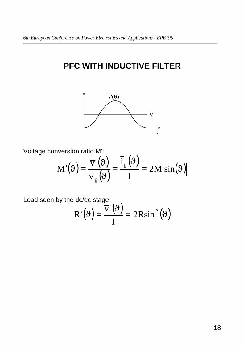
PFC WITH INDUCTIVE FILTER
ASSUMPTIONS:
o constant output current
o unity efficiency
o no low-frequency pulsating energy stored in the dc/dc stage
( ) ( ) ( )ϑ=ϑ
=ϑ 2i sinV2I
p'v
( )ϑ'v = average value of ( )ϑ'v in a switching period
6th European Conference on Power Electronics and Applications - EPE '95
18
PFC WITH INDUCTIVE FILTER
Voltage conversion ratio M':
( ) ( )( )
( ) ( )ϑ=ϑ
=ϑϑ
=ϑ′ sinM2I
i
v'v
M g
g
Load seen by the dc/dc stage:
( ) ( ) ( )ϑ=ϑ
=ϑ′ 2Rsin2I
'vR

6th European Conference on Power Electronics and Applications - EPE '95
19
POWER FACTOR CORRECTORS: STANDARDCONFIGURATION
TWO STAGE PFC: CASCADE CONNECTION
PREREGULATORS: AC/DC converters with high power factorand poor output voltage regulation
LOW EFFICIENCY: THE SAME POWER IS PROCESSED TWICE

6th European Conference on Power Electronics and Applications - EPE '95
20
BASIC PREREGULATORS: BOOST TOPOLOGY
CHARACTERISTICS:
o Inherent input filter (low input current harmonic content)
o Simple topology
o high power factor
o Output voltage greater than peak input voltage
o no start-up or short circuit protection
o no high-frequency insulation

6th European Conference on Power Electronics and Applications - EPE '95
21
BASIC PREREGULATORS: BOOST TOPOLOGY
CCM OPERATION
Assumption:
switching frequency much greater than line frequency(quasi-stationary approach).
Main waveforms in a switching period
6th European Conference on Power Electronics and Applications - EPE '95
22
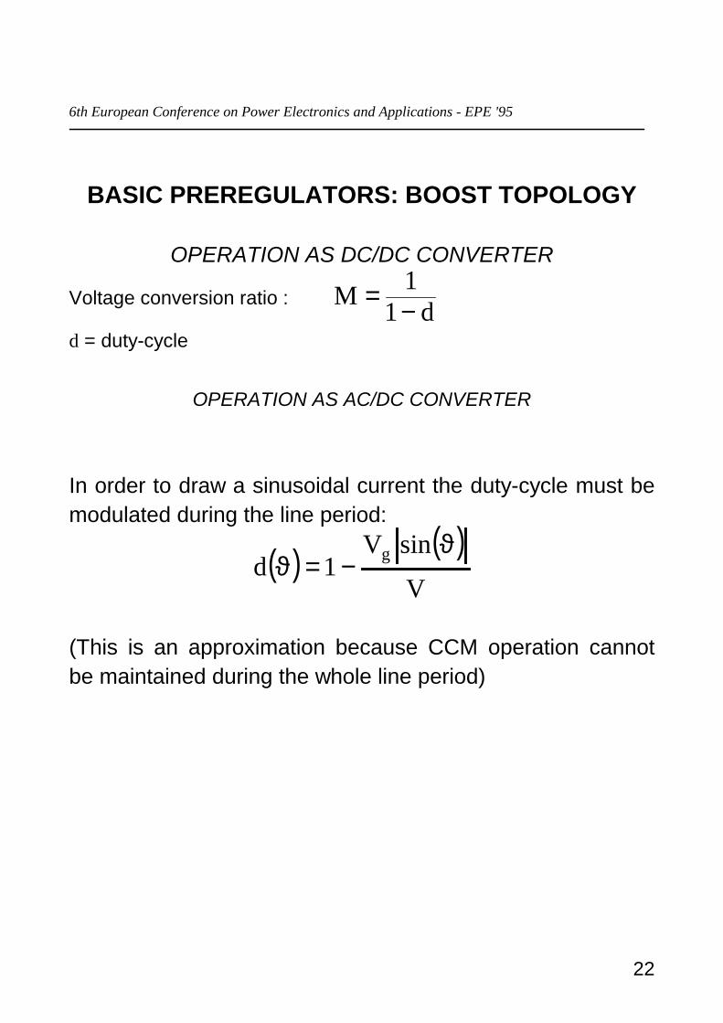
BASIC PREREGULATORS: BOOST TOPOLOGY
OPERATION AS DC/DC CONVERTER
Voltage conversion ratio : M d= −1
1d = duty-cycle
OPERATION AS AC/DC CONVERTER
In order to draw a sinusoidal current the duty-cycle must bemodulated during the line period:
( ) ( )V
sinV1d g ϑ
−=ϑ
(This is an approximation because CCM operation cannotbe maintained during the whole line period)

6th European Conference on Power Electronics and Applications - EPE '95
23
BASIC PREREGULATORS: BUCK + BOOSTTOPOLOGY
CHARACTERISTICS:
o S1 and D1 provide start-up and short circuit protection
o buck-mode operation for vg higher than output voltageand boost mode-operation for vg lower than outputvoltage
o high conduction losses (four semiconductors in series)

6th European Conference on Power Electronics and Applications - EPE '95
24
BASIC PREREGULATORS: FLYBACK TOPOLOGY
CHARACTERISTICS:
o Simple topology
o high power factor with constant duty-cycle inDiscontinuous Conduction Mode (DCM) operation
o inherent start-up and short circuit protection
o high-frequency insulation transformer
o high input current harmonic content

6th European Conference on Power Electronics and Applications - EPE '95
25
BASIC PREREGULATORS: FLYBACK TOPOLOGY
DCM OPERATION
Main waveforms in a switching period
6th European Conference on Power Electronics and Applications - EPE '95
26
BASIC PREREGULATORS: FLYBACK TOPOLOGY
DCM OPERATION
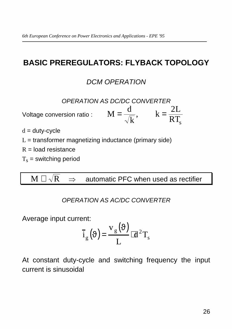
OPERATION AS DC/DC CONVERTER
Voltage conversion ratio : M dk
k LRTs
= =, 2
d = duty-cycleL = transformer magnetizing inductance (primary side)R = load resistanceTs = switching period
M R∝ automatic PFC when used as rectifier
OPERATION AS AC/DC CONVERTER
Average input current:
( ) ( )s
2gg Td
L
vi ⋅
ϑ=ϑ
At constant duty-cycle and switching frequency the inputcurrent is sinusoidal
6th European Conference on Power Electronics and Applications - EPE '95
27
CONTROL TECHNIQUES FOR SINGLE-PHASE
PFC'S AND COMMERCIAL CONTROL IC'S

6th European Conference on Power Electronics and Applications - EPE '95
28
BOOST PREREGULATOR
PEAK CURRENT CONTROL
Input current waveform

6th European Conference on Power Electronics and Applications - EPE '95
29
PEAK CURRENT CONTROL
CHARACTERISTICS:
o CONSTANT SWITCHING FREQUENCY
o CONTINUOUS CONDUCTION MODE (CCM) OPERATION
- low device current stresses
- low RMS current
- small EMI filter
o POSSIBILITY TO SENSE ONLY SWITCH CURRENT
- efficiency improvement
- possibility to implement a pulse-by-pulse current limit
o SUBHARMONIC OSCILLATIONS (for duty-cycle > 50%)
o LINE CURRENT DISTORTION (increases for high linevoltages, light load and high amplitude of compensating ramp)
o COMMUTATION NOISE SENSITIVITY
o HARD REVERSE RECOVERY OF FREEWHEELING DIODE(increased commutation losses and EMI)

6th European Conference on Power Electronics and Applications - EPE '95
30
PEAK CURRENT CONTROL
IDEAL REFERENCE CURRENT WAVEFORMS
0
1
2
3
0Ti
I ref[A]
0
0.4
0.8
0Ti
I ref[A]
Vi=115Vrms Vi=230Vrms
DISTORTION REDUCTION TECHNIQUES
o ADDING A DC OFFSET TO CURRENT REFERENCE
(function of both line voltage and load current)
o PROGRAMMED DISTORTION CURRENT REFERENCE
- line dependent DC offset
- constant offset plus soft clamp
6th European Conference on Power Electronics and Applications - EPE '95
31
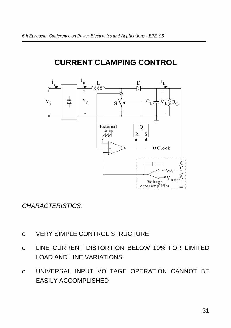
CURRENT CLAMPING CONTROL
CHARACTERISTICS:
o VERY SIMPLE CONTROL STRUCTURE
o LINE CURRENT DISTORTION BELOW 10% FOR LIMITEDLOAD AND LINE VARIATIONS
o UNIVERSAL INPUT VOLTAGE OPERATION CANNOT BEEASILY ACCOMPLISHED

6th European Conference on Power Electronics and Applications - EPE '95
32
BOOST PREREGULATOR
AVERAGE CURRENT CONTROL
Input current waveform

6th European Conference on Power Electronics and Applications - EPE '95
33
AVERAGE CURRENT CONTROL
CHARACTERISTICS:
o CONSTANT SWITCHING FREQUENCY
o CONTINUOUS CONDUCTION MODE (CCM) OPERATION
- low device current stresses
- low RMS current
- small EMI filter
o COMPLEX CONTROL SCHEME
- need of inductor current sensing
- need of a multiplier
o COMMUTATION NOISE IMMUNITY
o HARD REVERSE RECOVERY OF FREEWHEELING DIODE(increased commutation losses and EMI)
o SEVERAL CONTROL IC's AVAILABLE
6th European Conference on Power Electronics and Applications - EPE '95
34
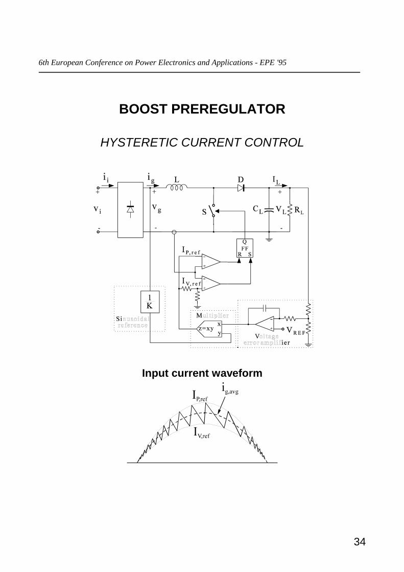
BOOST PREREGULATOR
HYSTERETIC CURRENT CONTROL
Input current waveform

6th European Conference on Power Electronics and Applications - EPE '95
35
HYSTERETIC CURRENT CONTROL
CHARACTERISTICS:
o WIDE SWITCHING FREQUENCY VARIATION
o CONTINUOUS CONDUCTION MODE (CCM) OPERATION
- low device current stresses
- low RMS current
- small EMI filter
o COMPLEX CONTROL SCHEME
- need of inductor current sensing
- need of a multiplier
o COMMUTATION NOISE SENSITIVITY
o HARD REVERSE RECOVERY OF FREEWHEELING DIODE(increased commutation losses and EMI)
o SMALL INPUT CURRENT DISTORTION NEAR ZEROCROSSING OF LINE VOLTAGE TO AVOID HIGHSWITCHING FREQUENCY

6th European Conference on Power Electronics and Applications - EPE '95
36
BOOST PREREGULATOR
BORDERLINE CONTROL(Operation at the boundary between DCM and CCM)
Input current waveform

6th European Conference on Power Electronics and Applications - EPE '95
37
BORDERLINE CONTROL
CHARACTERISTICS:
o AUTOMATIC PFC (CONSTANT SWITCH ON TIME)
o VARIABLE SWITCHING FREQUENCY (function of loadcurrent and instantaneous line voltage)
o DISCONTINUOUS CONDUCTION MODE (DCM)OPERATION
- high device current stresses
- high RMS current
- large EMI filter
- reduced switch turn on losses and increased turn offlosses
o SIMPLE CONTROL SCHEME
- no need for a multiplier (however some IC's make useof it)
- need for sensing the instant of inductor current zeroing
o SOFT RECOVERY OF FREEWHEELING DIODE

6th European Conference on Power Electronics and Applications - EPE '95
38
BOOST PREREGULATOR
DISCONTINUOUS CURRENT PWM CONTROL
Input current waveform
6th European Conference on Power Electronics and Applications - EPE '95
39
DISCONTINUOUS CURRENT PWM CONTROL
CHARACTERISTICS:o CONSTANT SWITCHING FREQUENCY
o DISCONTINUOUS CONDUCTION MODE (DCM)OPERATION
- high device current stresses
- high RMS current
- large EMI filter
- reduced switch turn on losses and increased turn offlosses
o NO NEED OF CURRENT SENSING
o SIMPLE PWM CONTROL
o INPUT CURRENT DISTORTION (WITH BOOSTCONVERTER)
- distortion can be reduced by subtracting a fraction ofrectified line voltage from the error voltage or bymodulating the clock frequency with rectified linevoltage
o SOFT RECOVERY OF FREEWHEELING DIODE
6th European Conference on Power Electronics and Applications - EPE '95
40
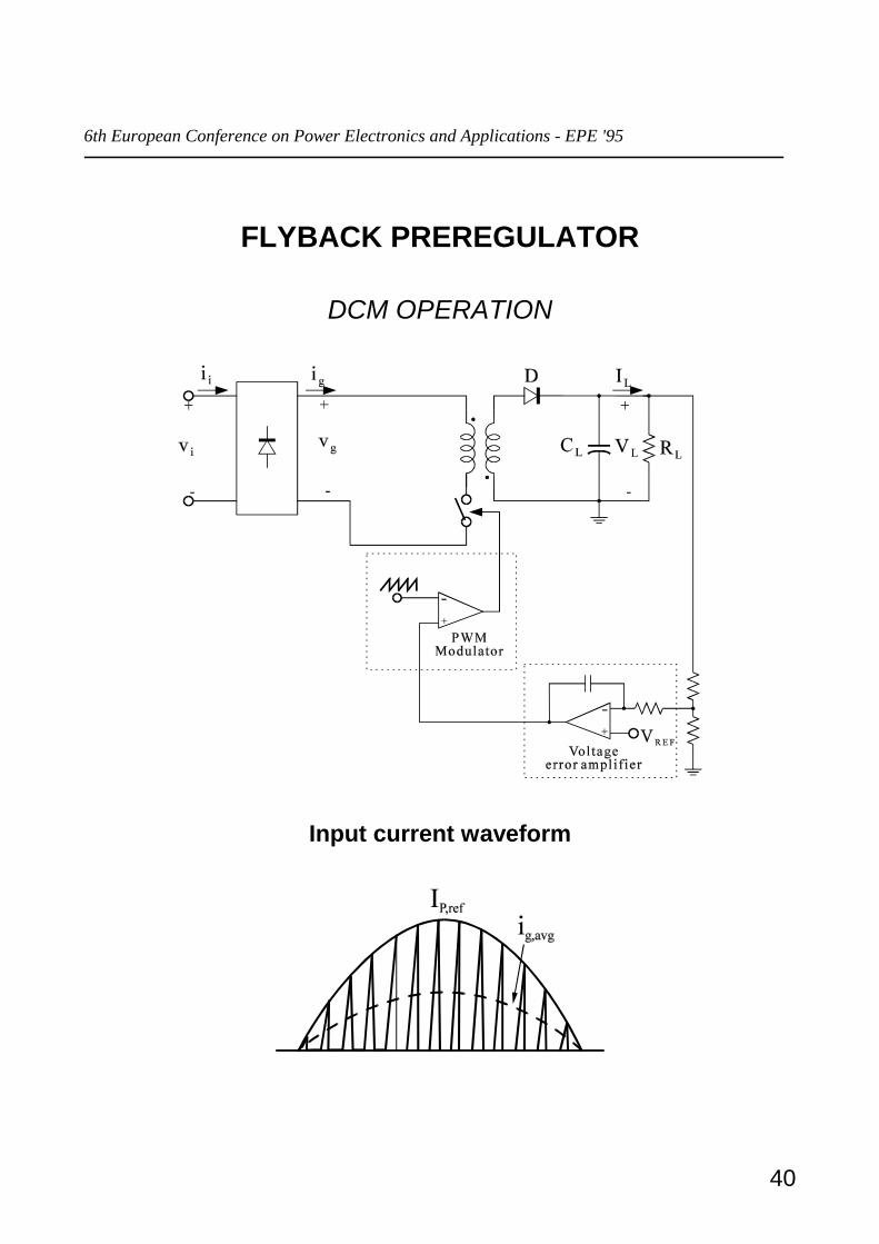
FLYBACK PREREGULATOR
DCM OPERATION
Input current waveform

6th European Conference on Power Electronics and Applications - EPE '95
41
DCM OPERATION
CHARACTERISTICS:
o AUTOMATIC PFC (CONSTANT SWITCH ON TIME)
o CONSTANT SWITCHING FREQUENCY
o DCM OPERATION
- high device current stresses
- high RMS current
- large EMI filter
- reduced switch turn on losses and increased turn offlosses
o NO NEED OF CURRENT SENSING
o SIMPLE PWM CONTROL
o SOFT OF RECOVERY OF FREEWHEELING DIODE

6th European Conference on Power Electronics and Applications - EPE '95
42
FLYBACK PREREGULATOR
CCM OPERATION - CHARGE CONTROL
Main waveforms
6th European Conference on Power Electronics and Applications - EPE '95
43
CCM OPERATION - CHARGE CONTROL
CHARACTERISTICS:
o CONSTANT SWITCHING FREQUENCY
o CONTINUOUS CONDUCTION MODE (CCM) OPERATION
- low device current stresses
- low RMS current
- relatively large EMI filter (current ripple is small, butinput current is discontinuous)
o SUBHARMONIC OSCILLATIONS (for duty-cycle > 50%)
o COMPLEX CONTROL SCHEME
- need of inductor current sensing
- need of a multiplier
o COMMUTATION NOISE IMMUNITY
o HARD REVERSE RECOVERY OF FREEWHEELING DIODE(increased commutation losses and EMI)

6th European Conference on Power Electronics and Applications - EPE '95
44
CONTROL IC'S
Constant frequency peakcurrent control
ML4812 (Micro Linear)TK84812 (Toko)
Constant frequencyaverage current control
UC1854/A/B family (Unitrode)UC1855 (Unitrode)TK3854A (Toko)ML4821 (Micro Linear)TDA4815, TDA4819 (Siemens)TA8310 (Toshiba)L4981A/B (SGS-Thomson)LT1248, LT1249 (Linear Tech.)
Hysteretic control CS3810 (Cherry Semic.)Borderline control TDA4814, TDA4816,
TDA4817, TDA4818 (Siemens)SG3561 (Silicon General)UC1852 (Unitrode)MC33261,MC33262(Motorola)L6560 (SGS-Thomson)
Two stage PFC withaverage-current control
UC1891/2/3/4 family (Unitrode)ML4824, ML4826 (Micro Linear)TK65030 (Toko)
Two stage PFC withpeak-current control
ML4819 (Micro Linear)TK84819 (Toko)
Buck-boost constantfrequency automaticcontrol
ML4813 (Micro Linear)

6th European Conference on Power Electronics and Applications - EPE '95
45
INSULATED POWER FACTOR CORRECTOR
TOPOLOGIES

6th European Conference on Power Electronics and Applications - EPE '95
46
PREREGULATORS BASED ON CUK AND SEPICCONVERTERS
DCM OPERATION
Cuk converter
Sepic converter
6th European Conference on Power Electronics and Applications - EPE '95
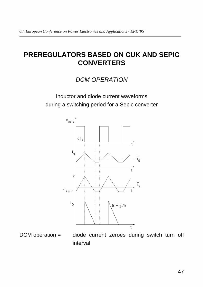
47
PREREGULATORS BASED ON CUK AND SEPICCONVERTERS
DCM OPERATION
Inductor and diode current waveformsduring a switching period for a Sepic converter
DCM operation = diode current zeroes during switch turn offinterval
6th European Conference on Power Electronics and Applications - EPE '95
48
PREREGULATORS BASED ON CUK AND SEPICCONVERTERS
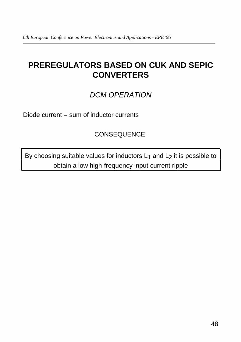
DCM OPERATION
Diode current = sum of inductor currents
CONSEQUENCE:
By choosing suitable values for inductors L1 and L2 it is possible toobtain a low high-frequency input current ripple
6th European Conference on Power Electronics and Applications - EPE '95
49
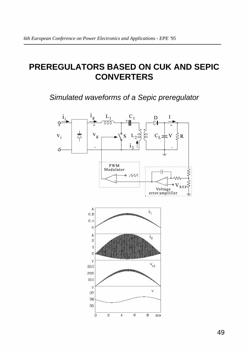
PREREGULATORS BASED ON CUK AND SEPICCONVERTERS
Simulated waveforms of a Sepic preregulator
Vc1
V

6th European Conference on Power Electronics and Applications - EPE '95
50
CUK PREREGULATORS
CHARACTERISTICS:
o CONSTANT SWITCHING FREQUENCY
o GOOD TRANSFORMER EXPLOITATION
o DCM OPERATION
- high device current stresses
- small EMI filter
- reduced switch turn on losses and increased turn offlosses
- soft diode turn off
o SIMPLE CONTROL SCHEME
- no need of current sensing
- no need of multiplier
o POSSIBILITY OF MAGNETIC COUPLING (REDUCTION OFMAGNETIC STRUCTURE SIZE AND INPUT CURRENTRIPPLE)
6th European Conference on Power Electronics and Applications - EPE '95
51
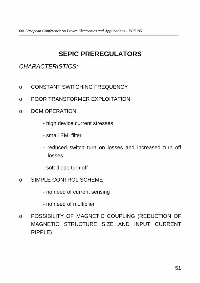
SEPIC PREREGULATORS
CHARACTERISTICS:
o CONSTANT SWITCHING FREQUENCY
o POOR TRANSFORMER EXPLOITATION
o DCM OPERATION
- high device current stresses
- small EMI filter
- reduced switch turn on losses and increased turn offlosses
- soft diode turn off
o SIMPLE CONTROL SCHEME
- no need of current sensing
- no need of multiplier
o POSSIBILITY OF MAGNETIC COUPLING (REDUCTION OFMAGNETIC STRUCTURE SIZE AND INPUT CURRENTRIPPLE)

6th European Conference on Power Electronics and Applications - EPE '95
52
PREREGULATORS BASED ON CUK AND SEPICCONVERTERS
CCM OPERATION
EXAMPLE: Sepic converter with average current mode
control
PROBLEM: design of the inner current loop

6th European Conference on Power Electronics and Applications - EPE '95
53
PREREGULATORS BASED ON CUK AND SEPICCONVERTERS
CCM OPERATION
Transfer function between duty-cycle and input current:
( )
⋅
+′′′′
+⋅
⋅′′
+⋅′′+
⋅+′′
=2
12
22
121
2122
D
c
12
22
Did
sLDLD
CLL1s
sDCLsL
DD
VI1
LDLDDV
sG
where D'=1-D.
APPROXIMATION: G s VsLid
D( ) ≈1
VD depends on input voltage
(for the boost preregulator is: G s VsLid ( ) ≈ , i.e. constant gain)
Sepic CukVD V V ng + V V ng +
Ic I I1 2+ I n I1 2+′C1 C1 C n C
C n Ca b
a b
⋅+
2
2
′L2 L2 L n22
6th European Conference on Power Electronics and Applications - EPE '95
54
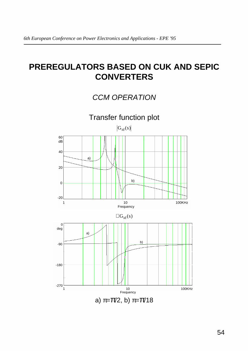
PREREGULATORS BASED ON CUK AND SEPICCONVERTERS
CCM OPERATION
Transfer function plotG sid ( )
1 10 100KHz
60
40
20
0
-20
dB
Frequency
a)
b)
∠ G sid ( )0
-90
-180
-2701 10 100KHz
deg
Frequency
a)
b)
a) π=π/2, b) π=π/18

6th European Conference on Power Electronics and Applications - EPE '95
55
PREREGULATORS BASED ON CUK AND SEPICCONVERTERS
CCM OPERATIONA damping Rd-Cd network across energy transfer capacitorC1 is used to properly shape the transfer function
G sid ( )
1 10 100KHz
40
20
0
-20
60dB
Frequency
a)
b)
∠ G sid ( )
1 10 100KHzFrequency
a)
b)
0
-90
-180
deg
a) ππππ=ππππ2, b) ππππ=ππππ/18
6th European Conference on Power Electronics and Applications - EPE '95
56
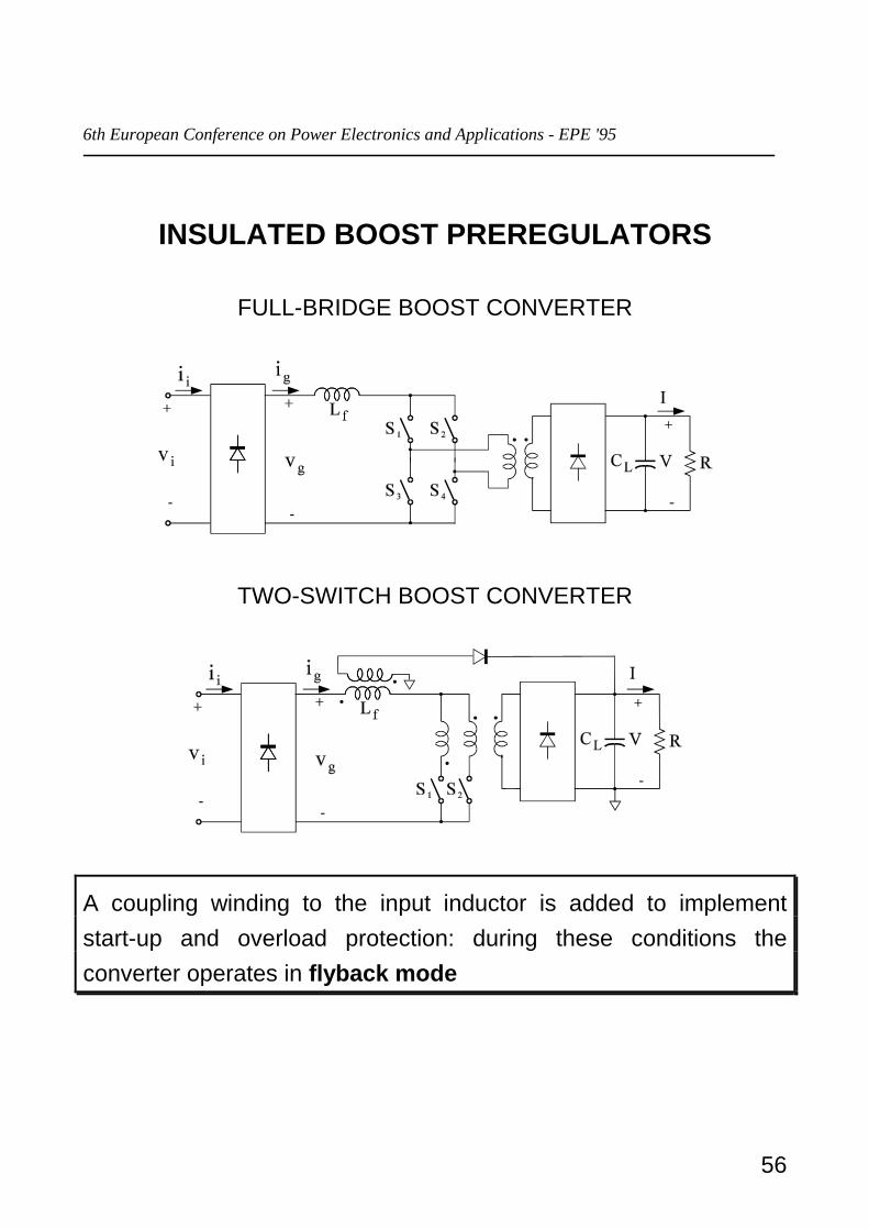
INSULATED BOOST PREREGULATORS
FULL-BRIDGE BOOST CONVERTER
TWO-SWITCH BOOST CONVERTER
A coupling winding to the input inductor is added to implementstart-up and overload protection: during these conditions theconverter operates in flyback mode
6th European Conference on Power Electronics and Applications - EPE '95
57
INSULATED BOOST PREREGULATORS
CHARACTERISTICS:
DIFFICULT TRANSFORMER IMPLEMENTATION
- low leakage inductance is essential
NEED OF A SUITABLE CLAMP CIRCUIT
HIGH VOLTAGE STRESS IN THE TWO-SWITCHIMPLEMENTATION
6th European Conference on Power Electronics and Applications - EPE '95
58
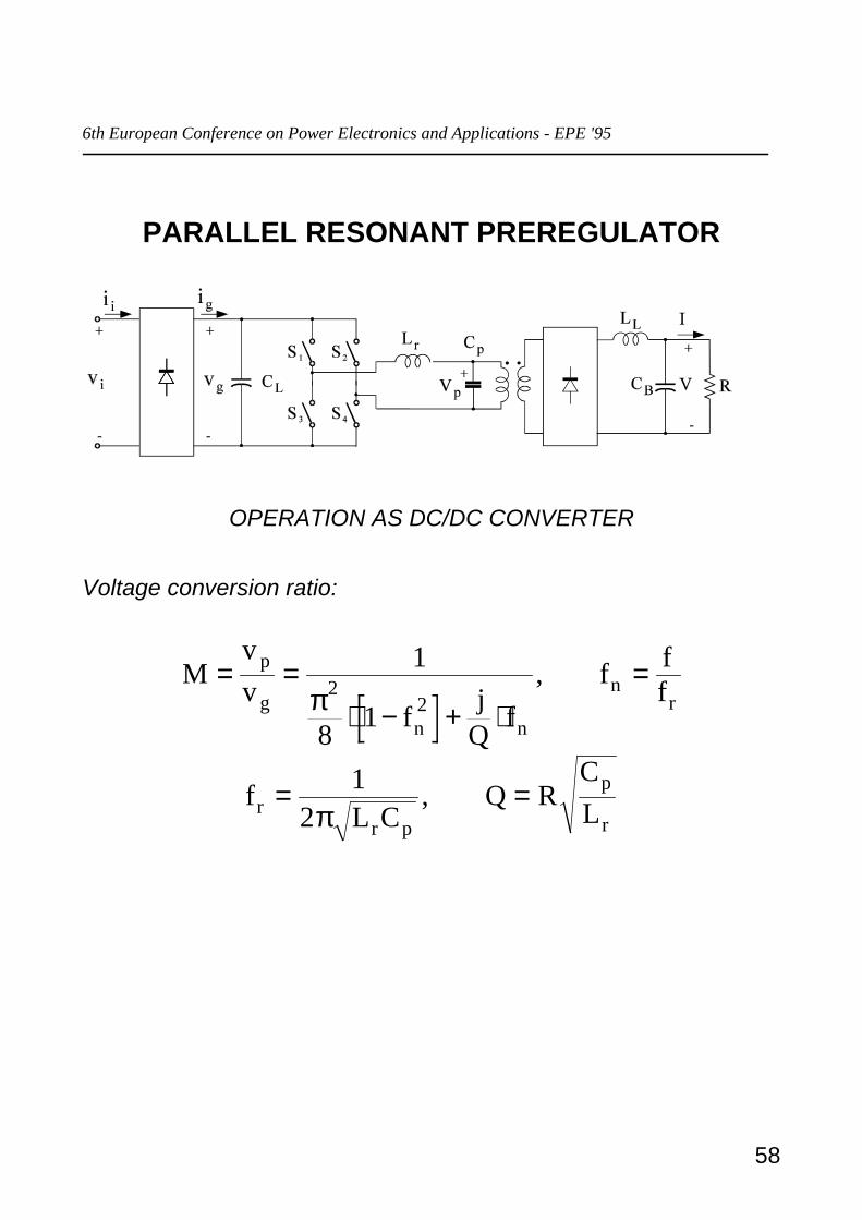
PARALLEL RESONANT PREREGULATOR
OPERATION AS DC/DC CONVERTER
Voltage conversion ratio:
Mvv
f jQ f
f ff
p
gn n
nr
= =⋅ − + ⋅
=1
8 12
2π,
fL C
Q RCLr
r p
p
r= =1
2π,

6th European Conference on Power Electronics and Applications - EPE '95
59
PARALLEL RESONANT PREREGULATOR
GAIN CHARACTERISTICS
0.4 0.6 0.8 1 1.2 1.4 1.6 1.8 20
1
2
3
4
5
f n
M
1
2
3
4Q=5

6th European Conference on Power Electronics and Applications - EPE '95
60
PARALLEL RESONANT PREREGULATOR
OPERATION AS AC/DC CONVERTER
( ) ( )( ) r
2r Z
1sin2
RZ'R
Q ⋅θ
=θ
=θ
Q factor variation during a half line cycle
0 π0
4
8
12
16
20
Q ( )θ
θ2π
Qmin=2
Near the zero crossing the circuit is lightly damped HIGH GAIN
Near the peak of ac line the circuit is heavily damped LOW GAIN

6th European Conference on Power Electronics and Applications - EPE '95
61
PARALLEL RESONANT PREREGULATOR
OPERATION AS AC/DC CONVERTER
CONSEQUENCE:
Good power factor (>90%) is obtained without activecontrol of the line current.
NOTE:The same result holds also for the series/parallel (LCC) resonantconverter. For this converter, an active control is necessary tomaintain zero voltage switching condition (operation must remain onthe right side of resonant peaks in all operating conditions)

6th European Conference on Power Electronics and Applications - EPE '95
62
FAST RESPONDING POWER FACTORCORRECTOR TOPOLOGIES
OBJECTIVES:
COMPACTNESS
HIGH POWER FACTOR
TIGHT AND FAST OUTPUT VOLTAGE REGULATION
HIGH-FREQUENCY INSULATION
6th European Conference on Power Electronics and Applications - EPE '95
63
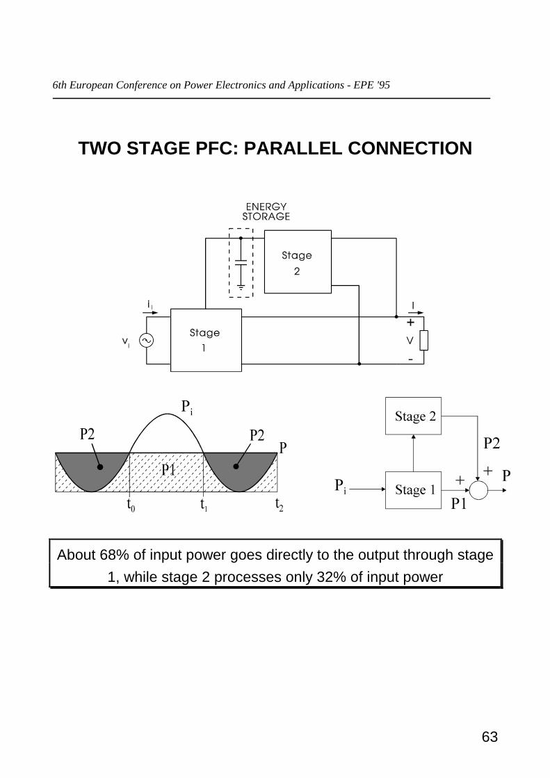
TWO STAGE PFC: PARALLEL CONNECTION
About 68% of input power goes directly to the output through stage1, while stage 2 processes only 32% of input power

6th European Conference on Power Electronics and Applications - EPE '95
64
TWO STAGE PFC: PARALLEL CONNECTION
Pi < P
• Boost converter controls power factor• Forward converter regulates output• CB stores energy• CL is small

6th European Conference on Power Electronics and Applications - EPE '95
65
TWO STAGE PFC: PARALLEL CONNECTION
Pi > P
• t2 controls power factor• t3 regulates output

6th European Conference on Power Electronics and Applications - EPE '95
66
SINGLE STAGE PFC: PARALLEL POWERPROCESSING
o need for several switches
o complex control
o discontinuous input current at least for a part of the line cycle(large EMI filter)

6th European Conference on Power Electronics and Applications - EPE '95
67
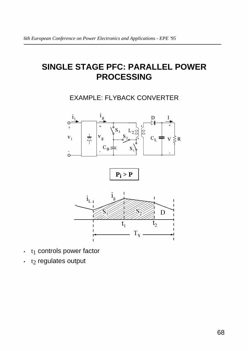
SINGLE STAGE PFC: PARALLEL POWERPROCESSING
EXAMPLE: FLYBACK CONVERTER
Pi < P
• t2 controls power factor• t1 regulates output• CB stores energy• CL is small
6th European Conference on Power Electronics and Applications - EPE '95
68
SINGLE STAGE PFC: PARALLEL POWERPROCESSING
EXAMPLE: FLYBACK CONVERTER
Pi > P
• t1 controls power factor• t2 regulates output

6th European Conference on Power Electronics and Applications - EPE '95
69
SINGLE STAGE PFC: BIFRED
(Boost Integrated with Flyback Rectifier/Energy storage/DC-DCconverter)
Main waveforms
• DCM input current ensures high power factor• duty-cycle regulates output• CB stores energy• CL is small
SINGLE STAGE PFC: BIBRED

6th European Conference on Power Electronics and Applications - EPE '95
70
(Boost Integrated with Buck Rectifier/Energy storage/DC-DCconverter)
Main waveforms
• DCM input current ensures high power factor• duty-cycle regulates output• CB stores energy• CL is small

6th European Conference on Power Electronics and Applications - EPE '95
71
SINGLE STAGE PFC: BIFRED, BIBRED
CHARACTERISTICS:
o DCM OPERATION
- high device current stresses
- big EMI filter
o TANK CAPACITOR VOLTAGE VB IS LOAD AND LINEDEPENDENT
- high device voltage stresses
- limited load range
SOLUTIONS:
o VARIABLE FREQUENCY CONTROL
- trade-off between voltage stress and frequency range ofcontrol
o DISCONTINUOUS OUTPUT CURRENT OPERATION

6th European Conference on Power Electronics and Applications - EPE '95
72
SINGLE STAGE PFC: S2IP2 FAMILY
(Single-Stage Isolated Power-factor corrected Power supplies)
COMBINING SWITCHES
a) when the off voltages are the sameb) when the off voltage of the left switch is always higher than the
off voltage of the right switchc) when the off voltage of a switch can be higher or lower than
the off voltage of the other switch
6th European Conference on Power Electronics and Applications - EPE '95
73
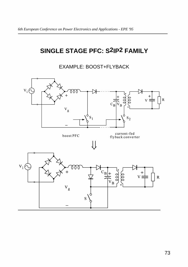
SINGLE STAGE PFC: S2IP2 FAMILY
EXAMPLE: BOOST+FLYBACK

6th European Conference on Power Electronics and Applications - EPE '95
74
SINGLE STAGE PFC: S2IP2 FAMILY
CHARACTERISTICS:
o SINGLE POWER STAGE WITH SINGLE HIGH-SPEEDCONTROL LOOP (PWM CONTROL)
o TANK CAPACITOR VOLTAGE VB INDEPENDENT OF LOADCURRENT
o DCM OPERATION OF BOTH PFC AND CURRENT-FEDDC/DC CONVERTER STAGES
- high device current stresses
- big EMI filter
6th European Conference on Power Electronics and Applications - EPE '95
75
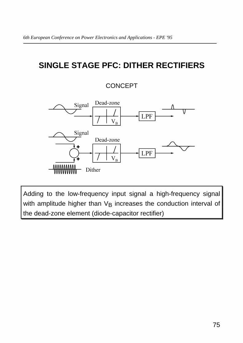
SINGLE STAGE PFC: DITHER RECTIFIERS
CONCEPT
Adding to the low-frequency input signal a high-frequency signalwith amplitude higher than VB increases the conduction interval ofthe dead-zone element (diode-capacitor rectifier)

6th European Conference on Power Electronics and Applications - EPE '95
76
SINGLE STAGE PFC: DITHER RECTIFIERS
EXAMPLE: VOLTAGE DOUBLER + HALF-BRIDGE CONVERTER
The connection is moved from point A to point B. In this way, thehigh-frequency signal present on the inverter leg is added to theinput voltage. An inductor is needed to smooth the input current.

6th European Conference on Power Electronics and Applications - EPE '95
77
SINGLE STAGE PFC: DITHER RECTIFIERS
EXAMPLE: VOLTAGE DOUBLER + HALF-BRIDGE CONVERTER
CHARACTERISTICS:
o DCM OPERATION
- high device current stresses
- big EMI filter
o TANK CAPACITOR VOLTAGE VB IS LOAD AND LINEDEPENDENT
- high device voltage stresses
- limited load range
o VARIABLE FREQUENCY CONTROL
6th European Conference on Power Electronics and Applications - EPE '95
78
TECHNIQUES FOR IMPROVING OUTPUT
VOLTAGE CONTROL SPEED
6th European Conference on Power Electronics and Applications - EPE '95
79
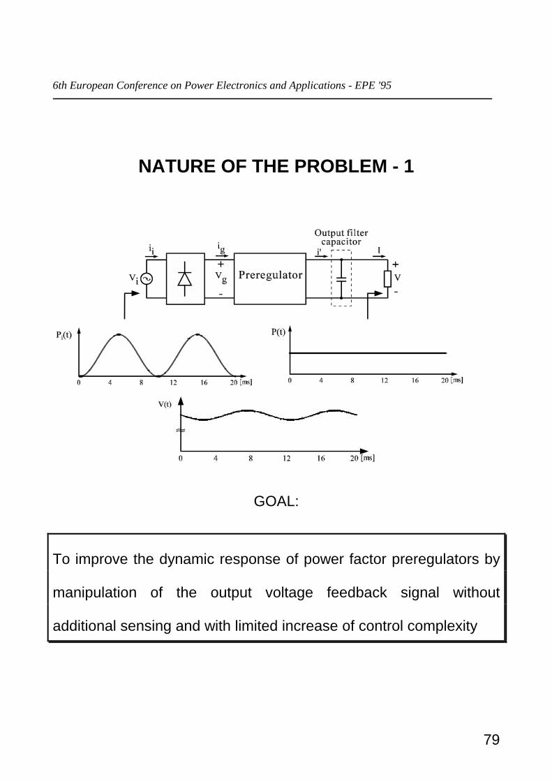
NATURE OF THE PROBLEM - 1
GOAL:
To improve the dynamic response of power factor preregulators by
manipulation of the output voltage feedback signal without
additional sensing and with limited increase of control complexity

6th European Conference on Power Electronics and Applications - EPE '95
80
NATURE OF THE PROBLEM - 2
Output voltage behavior:
( ) ( ) ( )t2sinVC2
PVtvVtv i
iDCDC ω⋅
ω−=∆+=
The voltage error signal contains a low-frequency ripple at twice the
line frequency
CONSEQUENCE:
the bandwidth of the voltage loop must be kept below the
line frequency in order to avoid input current distortion
6th European Conference on Power Electronics and Applications - EPE '95
81
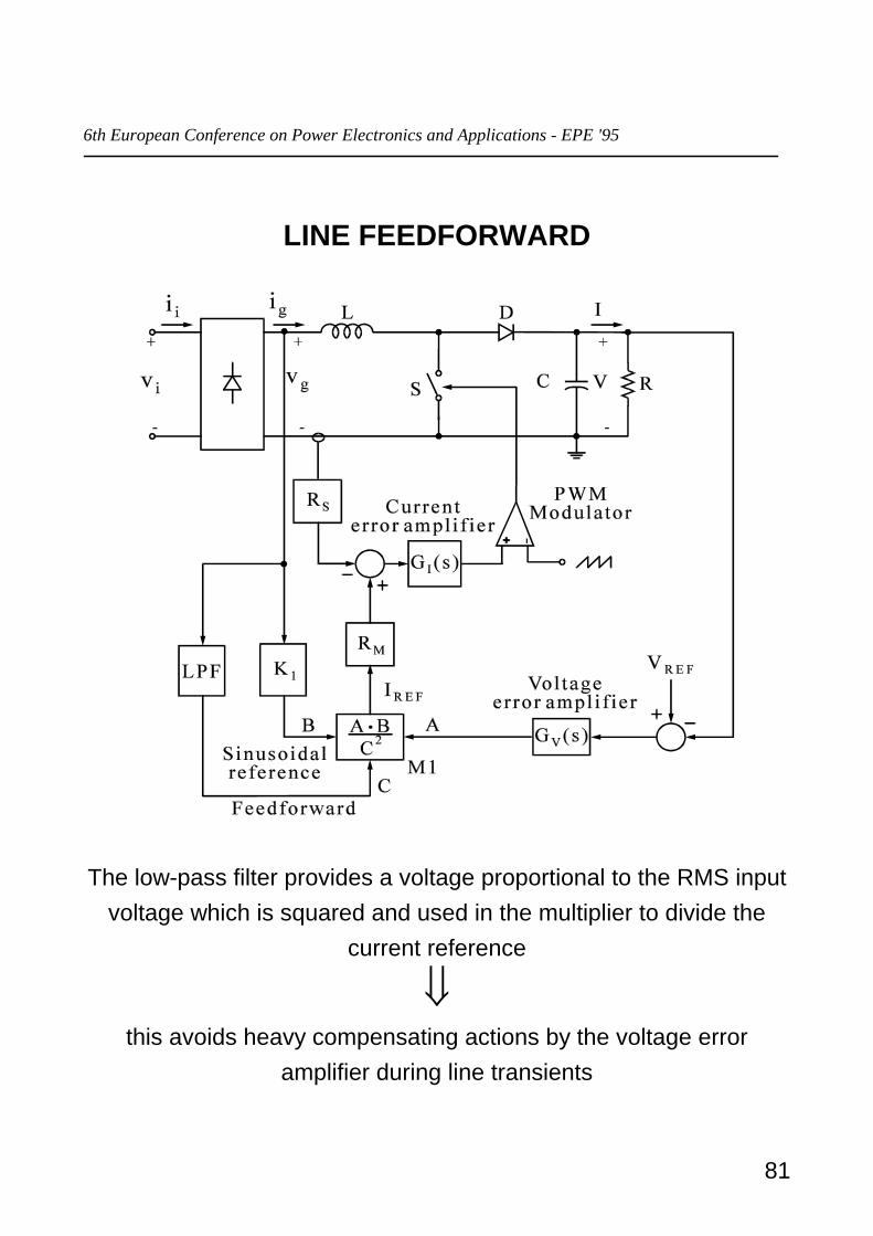
LINE FEEDFORWARD
The low-pass filter provides a voltage proportional to the RMS inputvoltage which is squared and used in the multiplier to divide the
current reference
this avoids heavy compensating actions by the voltage error
amplifier during line transients
6th European Conference on Power Electronics and Applications - EPE '95
82
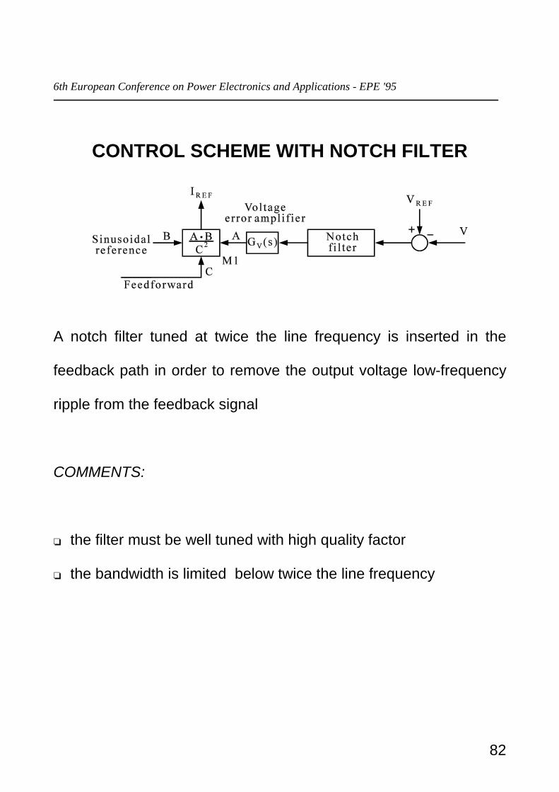
CONTROL SCHEME WITH NOTCH FILTER
A notch filter tuned at twice the line frequency is inserted in the
feedback path in order to remove the output voltage low-frequency
ripple from the feedback signal
COMMENTS:
the filter must be well tuned with high quality factor
the bandwidth is limited below twice the line frequency
6th European Conference on Power Electronics and Applications - EPE '95
83
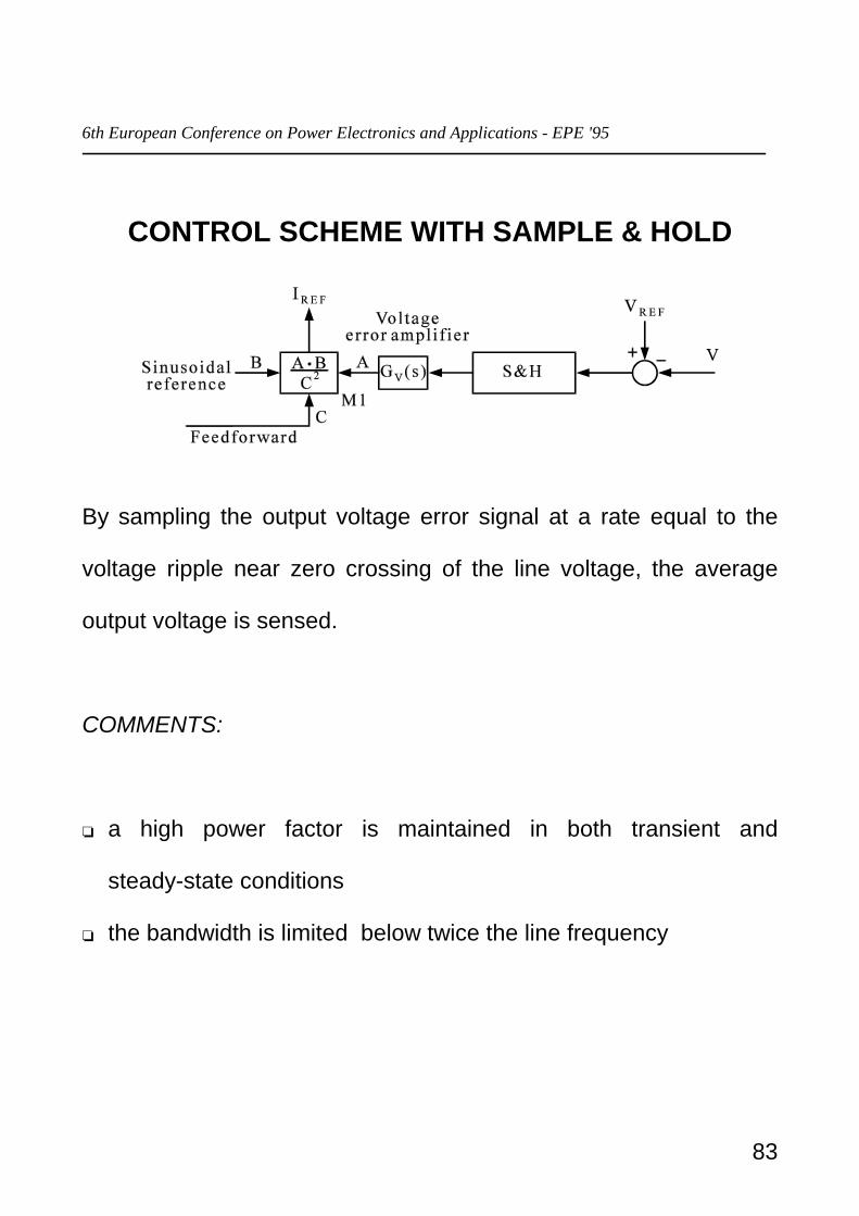
CONTROL SCHEME WITH SAMPLE & HOLD
By sampling the output voltage error signal at a rate equal to the
voltage ripple near zero crossing of the line voltage, the average
output voltage is sensed.
COMMENTS:
a high power factor is maintained in both transient and
steady-state conditions
the bandwidth is limited below twice the line frequency

6th European Conference on Power Electronics and Applications - EPE '95
84
CONTROL SCHEME WITH RIPPLECOMPENSATION
( ) ( )t2sinVC2
Ptv i
i
ω⋅ω
−=∆
The output voltage ripple is estimated and subtracted to thefeedback signal so that the error amplifier processes a ripple-freesignal
Under unity power factor condition, input power is given by:
( ) ( )t2cos2P
Ptp ii ω⋅η
−η=
where h is converter efficiency.
Error signal ∆v(t) can be estimated from input power signal through:
Elimination of DC component Phase shifting of ninety degrees Multiplication by a proper gain

6th European Conference on Power Electronics and Applications - EPE '95
85
CONTROL SCHEME WITH RIPPLECOMPENSATION
( ) sKsG cc ⋅=
COMMENTS:
in the presence of distorted input voltage, network Gc(s) turns outto be complicated
a second multiplier is needed
the bandwidth can be increased above twice the line frequency

6th European Conference on Power Electronics and Applications - EPE '95
86
CONTROL SCHEME WITH "REGULATION BAND"
REGULATION BAND APPROACH TYPE 1
The current reference amplitude is kept constant as long as theoutput voltage remains within a defined regulation band. When theoutput voltage goes outside of this band a high gain controllerchanges rapidly the current reference amplitude so as to bring theoutput voltage back into the regulation band
COMMENTS: correct average output voltage is obtained only at nominal
condition in which the voltage ripple amplitude is equal to thedead zone amplitude
slow input current dynamic response at load step changes

6th European Conference on Power Electronics and Applications - EPE '95
87
CONTROL SCHEME WITH "REGULATION BAND"
REGULATION BAND APPROACH TYPE 2
In order to overcome the problem represented by the steady-stateerror on the output voltage of the previous control technique, alow-bandwidth PI controller can be used which ensures stability andno DC errors. When the output voltage goes outside the band, thegain of the voltage error amplifier is increased in order to enhancethe corrective action
6th European Conference on Power Electronics and Applications - EPE '95
88
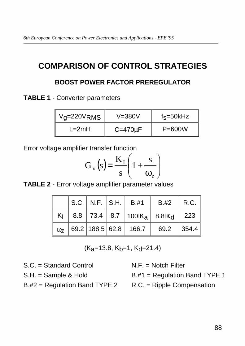
COMPARISON OF CONTROL STRATEGIES
BOOST POWER FACTOR PREREGULATOR
TABLE 1 - Converter parameters
Vg=220VRMS V=380V fs=50kHz
L=2mH C=470µF P=600W
Error voltage amplifier transfer function
( )
ω+=
z
Iv
s1
sK
sG
TABLE 2 - Error voltage amplifier parameter values
S.C. N.F. S.H. B.#1 B.#2 R.C.
KI 8.8 73.4 8.7 100⋅Ka 8.8⋅Kd 223
ωz 69.2 188.5 62.8 166.7 69.2 354.4
(Ka=13.8, Kb=1, Kd=21.4)
S.C. = Standard Control N.F. = Notch FilterS.H. = Sample & Hold B.#1 = Regulation Band TYPE 1B.#2 = Regulation Band TYPE 2 R.C. = Ripple Compensation
6th European Conference on Power Electronics and Applications - EPE '95
89
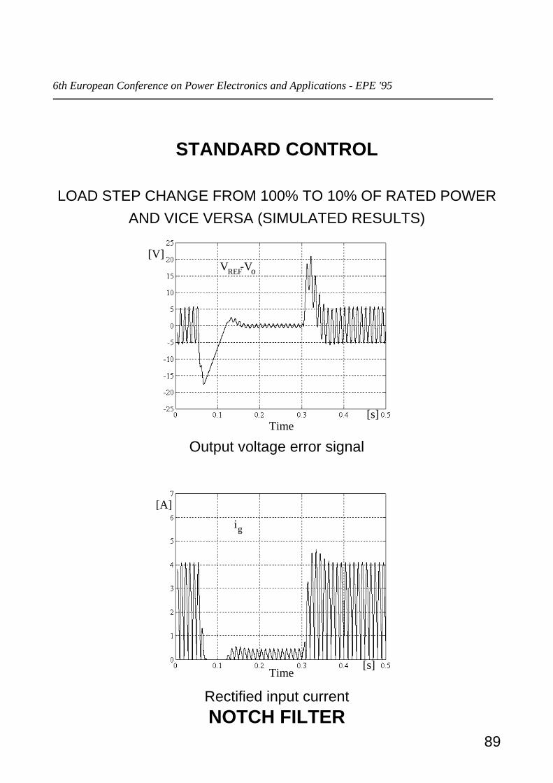
STANDARD CONTROL
LOAD STEP CHANGE FROM 100% TO 10% OF RATED POWERAND VICE VERSA (SIMULATED RESULTS)
V -VREF o
Time[s]
[V]
Output voltage error signal
ig
Time[s]
[A]
Rectified input currentNOTCH FILTER

6th European Conference on Power Electronics and Applications - EPE '95
90
LOAD STEP CHANGE FROM 100% TO 10% OF RATED POWERAND VICE VERSA (SIMULATED RESULTS)
V -VREF o
Time[s]
[V]
Output voltage error signal
ig
Time[s]
[A]
Rectified input current

6th European Conference on Power Electronics and Applications - EPE '95
91
SAMPLE & HOLD
LOAD STEP CHANGE FROM 100% TO 10% OF RATED POWERAND VICE VERSA (SIMULATED RESULTS)
V -VREF o
Time[s]
[V]
Output voltage error signal
ig
Time[s]
[A]
Rectified input current

6th European Conference on Power Electronics and Applications - EPE '95
92
REGULATION BAND TYPE 1
LOAD STEP CHANGE FROM 100% TO 10% OF RATED POWERAND VICE VERSA (SIMULATED RESULTS)
V -VREF o
Time[s]
[V]
Output voltage error signal
ig
Time[s]
[A]
Rectified input current
6th European Conference on Power Electronics and Applications - EPE '95
93
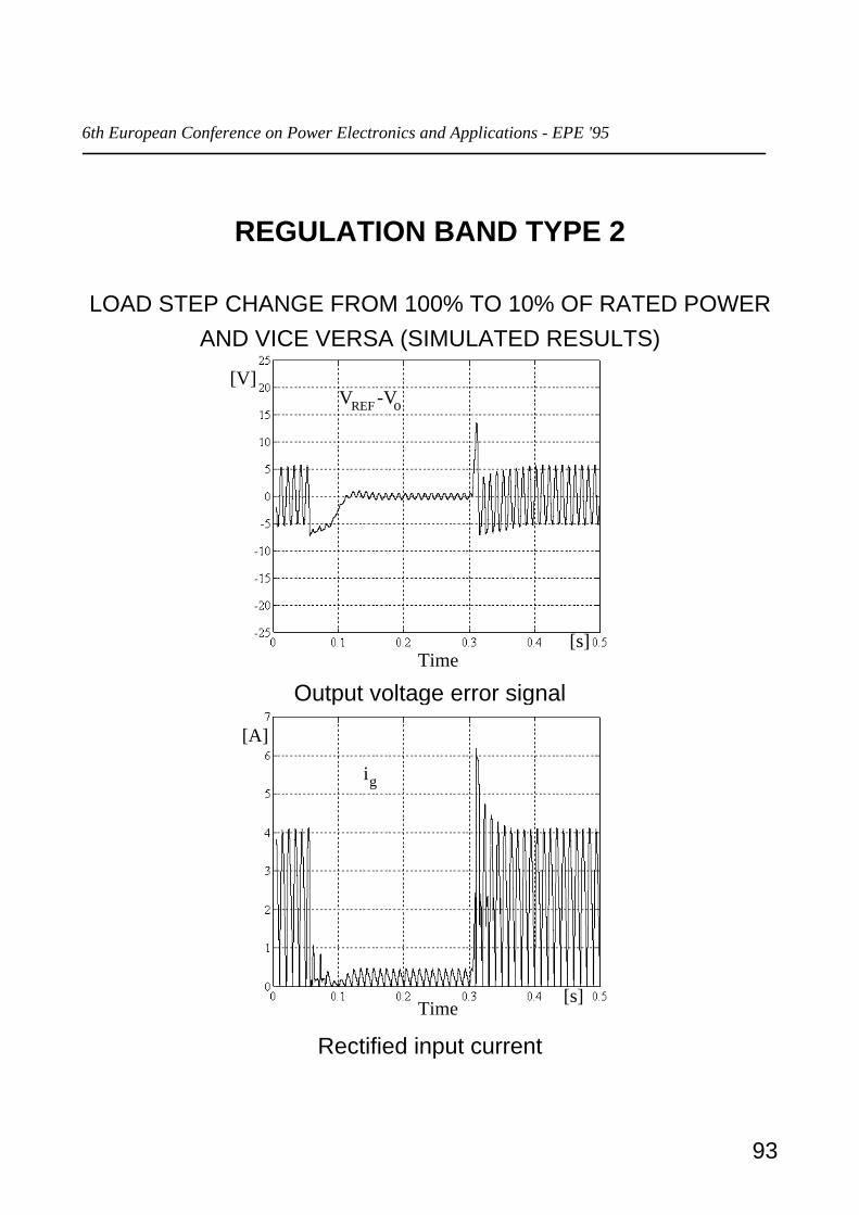
REGULATION BAND TYPE 2
LOAD STEP CHANGE FROM 100% TO 10% OF RATED POWERAND VICE VERSA (SIMULATED RESULTS)
V -VREF o
Time[s]
[V]
Output voltage error signal
ig
Time[s]
[A]
Rectified input current

6th European Conference on Power Electronics and Applications - EPE '95
94
RIPPLE COMPENSATION
LOAD STEP CHANGE FROM 100% TO 10% OF RATED POWERAND VICE VERSA (SIMULATED RESULTS)
V -VREF o
Time[s]
[V]
Output voltage error signal
ig
Time[s]
[A]
Rectified input current
6th European Conference on Power Electronics and Applications - EPE '95
95
BASICS OF SOFT-SWITCHINGTECHNIQUES
6th European Conference on Power Electronics and Applications - EPE '95
96
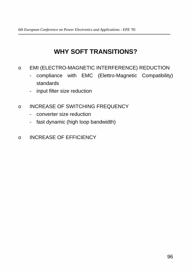
WHY SOFT TRANSITIONS?
o EMI (ELECTRO-MAGNETIC INTERFERENCE) REDUCTION- compliance with EMC (Elettro-Magnetic Compatibility)
standards- input filter size reduction
o INCREASE OF SWITCHING FREQUENCY- converter size reduction- fast dynamic (high loop bandwidth)
o INCREASE OF EFFICIENCY

6th European Conference on Power Electronics and Applications - EPE '95
97
SOFT SWITCHING SOLUTIONS
o QUASI-RESONANT OR RESONANT TOPOLOGIES
- increased current and/or voltage stresses
- increased conduction losses (resonant components inseries with main power path)
- difficulties to maintain soft-switching condition for wide lineand load ranges
o AUXILIARY CIRCUIT
- "PWM like" current and voltage waveforms
- need of an auxiliary switch
- little increase of control complexity
- soft-switching condition easily maintained for wide line andload ranges

6th European Conference on Power Electronics and Applications - EPE '95
98
REVERSE RECOVERY PROBLEM IN BOOSTRECTIFIERS
o INCREASED SWITCHING LOSSES
o INCREASED EMI
o INCREASED DEVICE CURRENT STRESSES
6th European Conference on Power Electronics and Applications - EPE '95
99
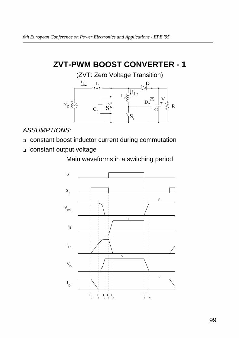
ZVT-PWM BOOST CONVERTER - 1(ZVT: Zero Voltage Transition)
ASSUMPTIONS: constant boost inductor current during commutation constant output voltage
Main waveforms in a switching period
S
S
I
I
I
V
V
r
DS
S
Lr
D
D
T T T T T T T1 2 3 4 5 60
V
V
I
I
L
L

6th European Conference on Power Electronics and Applications - EPE '95
100
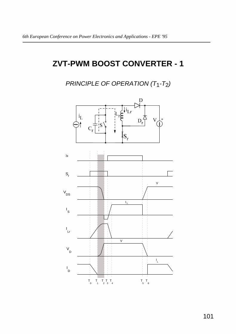
ZVT-PWM BOOST CONVERTER - 1
PRINCIPLE OF OPERATION (T0-T1)
S
S
I
I
I
V
V
r
DS
S
Lr
D
D
T T T T T T T1 2 3 4 5 60
V
V
I
I
L
L
6th European Conference on Power Electronics and Applications - EPE '95
101
ZVT-PWM BOOST CONVERTER - 1
PRINCIPLE OF OPERATION (T1-T2)
S
S
I
I
I
V
V
r
DS
S
Lr
D
D
T T T T T T T1 2 3 4 5 60
V
V
I
I
L
L
6th European Conference on Power Electronics and Applications - EPE '95
102
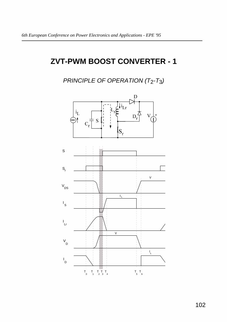
ZVT-PWM BOOST CONVERTER - 1
PRINCIPLE OF OPERATION (T2-T3)
S
S
I
I
I
V
V
r
DS
S
Lr
D
D
T T T T T T T1 2 3 4 5 60
V
V
I
I
L
L
6th European Conference on Power Electronics and Applications - EPE '95
103
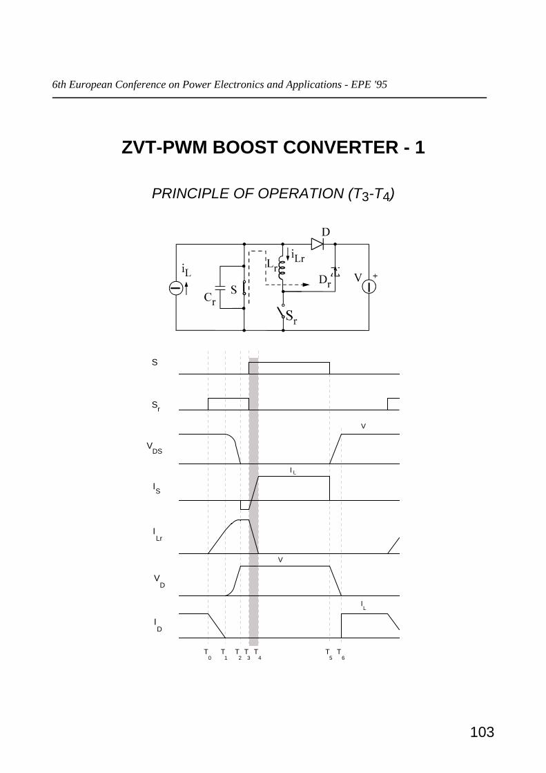
ZVT-PWM BOOST CONVERTER - 1
PRINCIPLE OF OPERATION (T3-T4)
S
S
I
I
I
V
V
r
DS
S
Lr
D
D
T T T T T T T1 2 3 4 5 60
V
V
I
I
L
L

6th European Conference on Power Electronics and Applications - EPE '95
104
ZVT-PWM BOOST CONVERTER - 1
PRINCIPLE OF OPERATION (T4-T5)
S
S
I
I
I
V
V
r
DS
S
Lr
D
D
T T T T T T T1 2 3 4 5 60
V
V
I
I
L
L

6th European Conference on Power Electronics and Applications - EPE '95
105
ZVT-PWM BOOST CONVERTER - 1
PRINCIPLE OF OPERATION (T5-T6)
S
S
I
I
I
V
V
r
DS
S
Lr
D
D
T T T T T T T1 2 3 4 5 60
V
V
I
I
L
L

6th European Conference on Power Electronics and Applications - EPE '95
106
ZVT-PWM BOOST CONVERTER - 1
PRINCIPLE OF OPERATION (T6-T0)
S
S
I
I
I
V
V
r
DS
S
Lr
D
D
T T T T T T T1 2 3 4 5 60
V
V
I
I
L
L
T0

6th European Conference on Power Electronics and Applications - EPE '95
107
ZVT-PWM BOOST CONVERTER - 1
CHARACTERISTICS:
o SOFT-SWITCHING FOR BOTH MAIN SWITCH ANDRECTIFIER
o CONSTANT FREQUENCY OPERATION
o HIGH EFFICIENCY
o ZERO-CURRENT TURN ON OF THE AUXILIARY SWITCH
o HARD TURN OFF OF THE AUXILIARY SWITCH
6th European Conference on Power Electronics and Applications - EPE '95
108
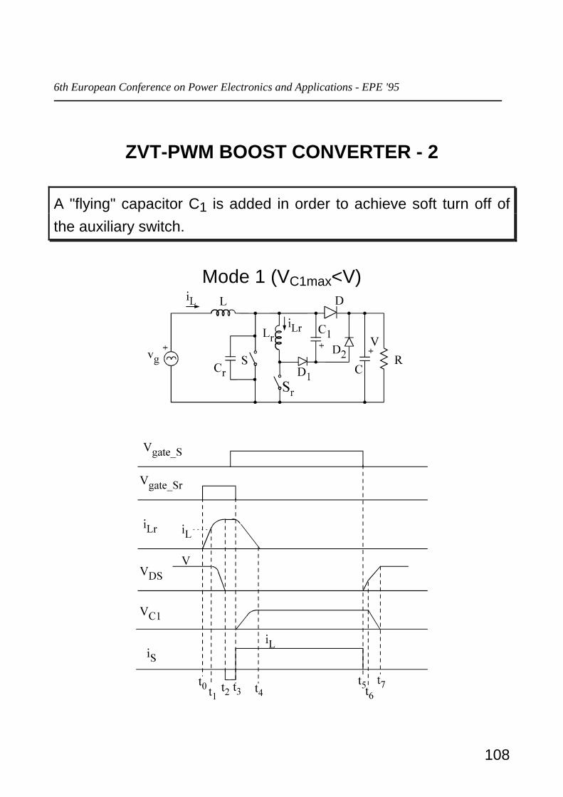
ZVT-PWM BOOST CONVERTER - 2
A "flying" capacitor C1 is added in order to achieve soft turn off ofthe auxiliary switch.
Mode 1 (VC1max<V)
6th European Conference on Power Electronics and Applications - EPE '95
109
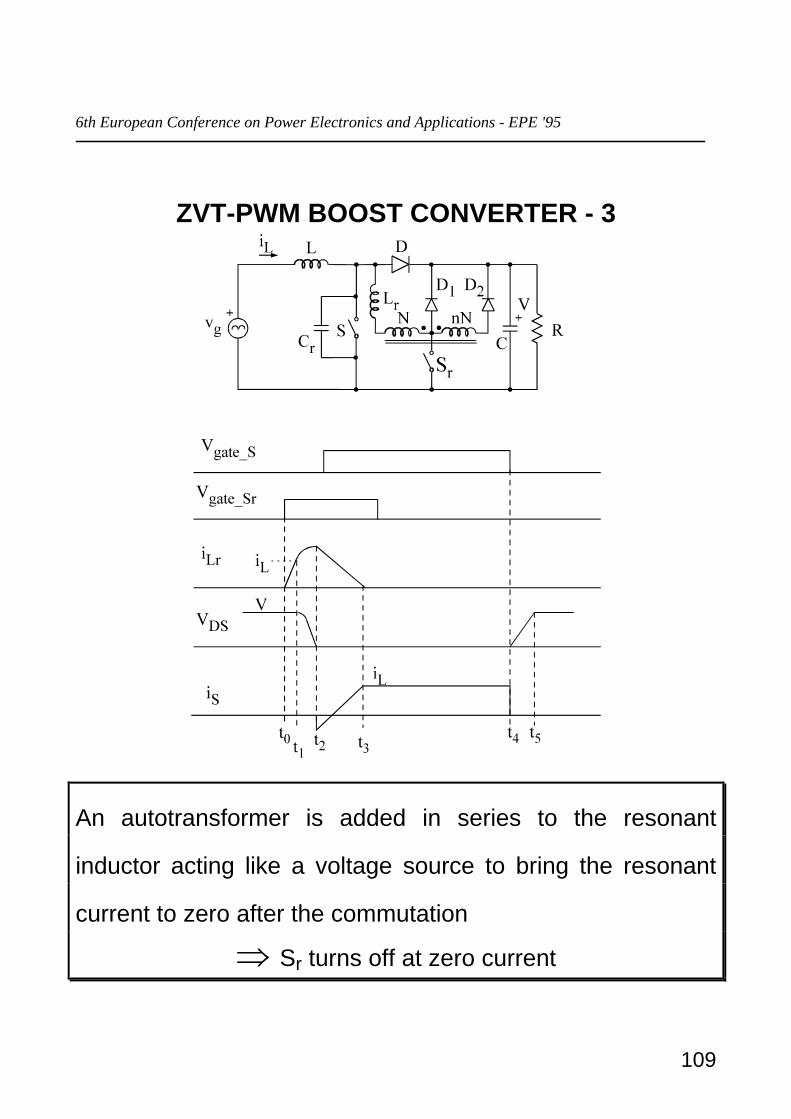
ZVT-PWM BOOST CONVERTER - 3
An autotransformer is added in series to the resonant
inductor acting like a voltage source to bring the resonant
current to zero after the commutation
Sr turns off at zero current

6th European Conference on Power Electronics and Applications - EPE '95
110
SMALL-SIGNAL MODELING

6th European Conference on Power Electronics and Applications - EPE '95
111
SMALL-SIGNAL MODEL OF A PFCOPERATING IN CCM
Power balance: v i v ii i⋅ = ⋅0 0
where
+=
+=
iii
iii
iIi
vVv (RMS values)
+=
+=
000
000
iIi
vVv
6th European Conference on Power Electronics and Applications - EPE '95
112
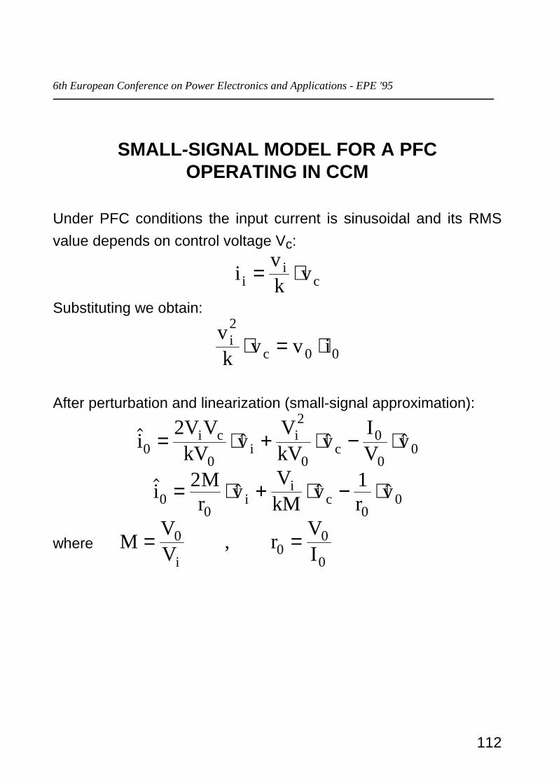
SMALL-SIGNAL MODEL FOR A PFCOPERATING IN CCM
Under PFC conditions the input current is sinusoidal and its RMSvalue depends on control voltage Vc:
ivk vi
ic= ⋅
Substituting we obtain:
vk v v ii
c
2
0 0⋅ = ⋅
After perturbation and linearization (small-signal approximation):
iV VkV v
VkV v
IV vi c
ii
c00
2
0
0
00
2= ⋅ + ⋅ − ⋅
i Mr v
VkM v r vi
ic0
0 00
2 1= ⋅ + ⋅ − ⋅
where MVV r
VIi
= =00
0
0,
6th European Conference on Power Electronics and Applications - EPE '95
113
SMALL-SIGNAL MODEL FOR A PFCOPERATING IN CCM
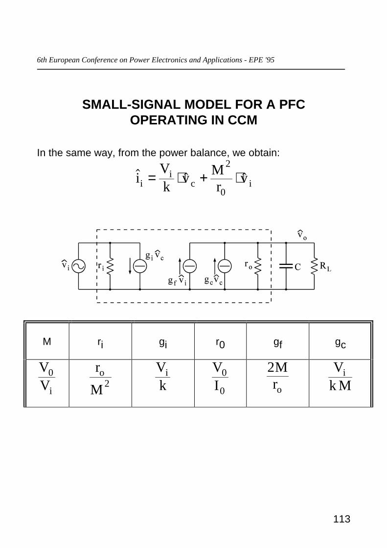
In the same way, from the power balance, we obtain:
iVk v M
r vii
c i= ⋅ + ⋅2
0
M ri gi r0 gf gc
VVi
0 rM
o2
Vk
i VI
0
0
2Mro
Vk M
i
6th European Conference on Power Electronics and Applications - EPE '95
114
SMALL-SIGNAL MODEL FOR A PFCOPERATING IN CCM
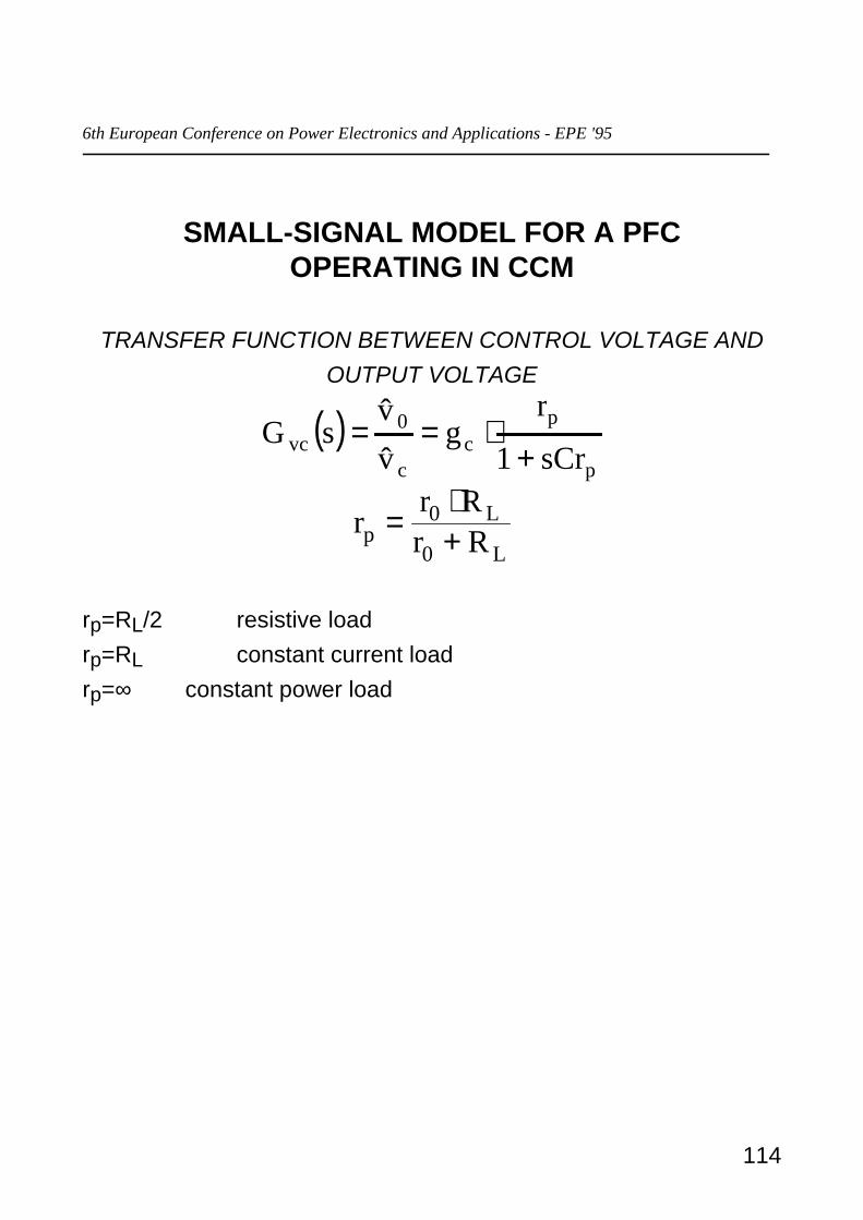
TRANSFER FUNCTION BETWEEN CONTROL VOLTAGE ANDOUTPUT VOLTAGE
( )p
pc
c
0vc sCr1
rg
vv
sG+
⋅==
rr Rr Rp
L
L=
⋅+
0
0
rp=RL/2 resistive loadrp=RL constant current loadrp=∞ constant power load
6th European Conference on Power Electronics and Applications - EPE '95
115
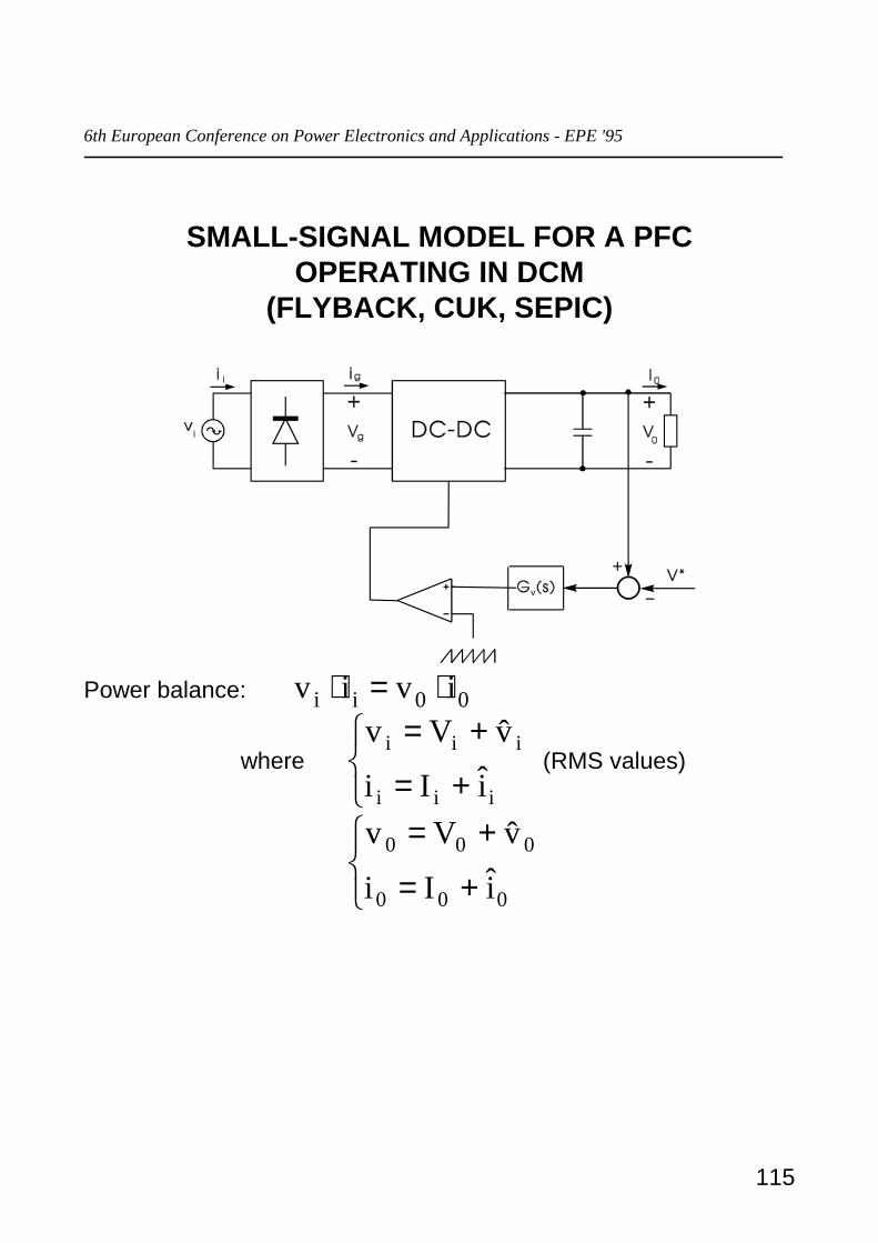
SMALL-SIGNAL MODEL FOR A PFCOPERATING IN DCM
(FLYBACK, CUK, SEPIC)
Power balance: v i v ii i⋅ = ⋅0 0
where
+=
+=
iii
iii
iIi
vVv (RMS values)
+=
+=
000
000
iIi
vVv

6th European Conference on Power Electronics and Applications - EPE '95
116
SMALL-SIGNAL MODEL FOR A PFCOPERATING IN DCM
Under PFC conditions the input current is sinusoidal and its RMSvalue depends on duty-cycle δ:
iT vLis i
eq= ⋅2
2δ
where Leq depends on converter topology.Substituting we obtain:
v TL v ii s
eq
22
0 02 ⋅ = ⋅δ
After perturbation and linearization (small-signal approximation):
iV Y D
V vV Y D
VIV vi i
ii i
0
2
0
2
0
0
00
2 2= ⋅ + ⋅ − ⋅δ
where YTLi
s
eq= 2

6th European Conference on Power Electronics and Applications - EPE '95
117
SMALL-SIGNAL MODEL FOR A PFCOPERATING IN DCM
iY DM v
V Y DM r vi
ii i
0
2
00
2 2 1= ⋅ + ⋅ − ⋅δ
where MVV r
VIi
= =00
0
0,
In the same way, from the power balance, we obtain: i V Y D D Y vi i i i i= ⋅ + ⋅2 2δ

6th European Conference on Power Electronics and Applications - EPE '95
118
SMALL-SIGNAL MODEL FOR A PFCOPERATING IN DCM
MODEL PARAMETERS
M ri gi r0 gf gcVVi
0 12D Yi
2DV Yi iVI
0
0
2 2Y DMi
2V Y DMi i
FLYBACK CUK SEPICLeq L L L
n L L1 2
21 2
⋅+
L LL L
1 2
1 2
⋅+
n=transformer turns ratio (N2/N1)
TRANSFER FUNCTION BETWEEN DUTY-CYCLEAND OUTPUT VOLTAGE
( )p
pc
0v sCr1
rgˆ
vsG
+⋅=
δ=
rr Rr Rp
L
L=
⋅+
0
0
6th European Conference on Power Electronics and Applications - EPE '95
119
DESIGN OF BOOST PFC OPERATING IN
CCM WITH AVERAGE CURRENT MODE
CONTROL

6th European Conference on Power Electronics and Applications - EPE '95
120
POWER STAGE SCHEME
L
D
C
C
ZS
S
Cf
f L
D
D
D
D
+
1 2
3 4
1
2
i
R s
J J1 2
4J
V0
+
-
J
R D ''
Vin
3J6
R
R
p
p
1
2
L
J5
CHARACTERISTICS:
Input voltage: Vin = 90-260VRMSOutput voltage: Vo = 380VOutput power: Po = 600WSwitching frequency: fs = 70kHz

6th European Conference on Power Electronics and Applications - EPE '95
121
POWER STAGE DESIGN
1) Inductor peak current (average value in a switching period)P Po g= ⋅ηwhere η is converter efficiency
ηη
⋅⋅
= =
I VP I
PV
L go L
o
g22
(1)
Worst case: minimum input voltage
..I AL = ⋅
⋅ ⋅=2 600
0 95 2 909 92
6th European Conference on Power Electronics and Applications - EPE '95
122
POWER STAGE DESIGN
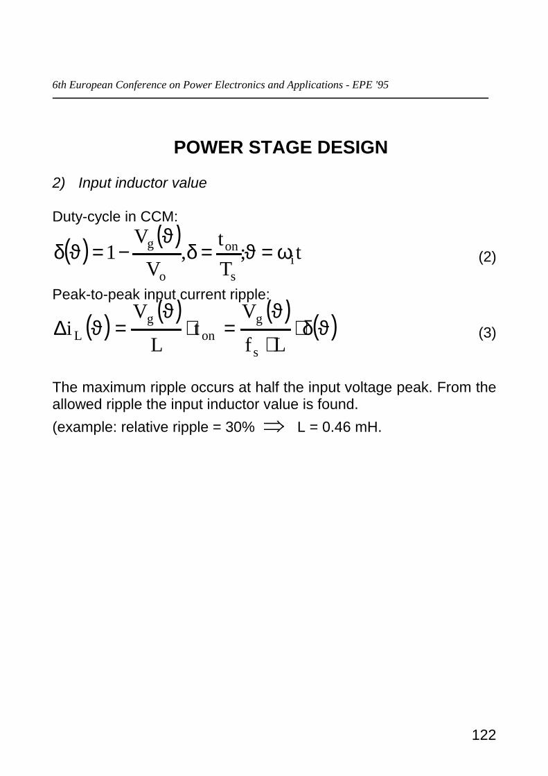
2) Input inductor value
Duty-cycle in CCM:
( ) ( )t;
Tt
,V
V1 i
s
on
o
g ω=ϑ=δϑ
−=ϑδ (2)
Peak-to-peak input current ripple:
( ) ( ) ( ) ( )ϑδ⋅⋅
ϑ=⋅
ϑ=ϑ∆
Lf
Vt
L
Vi
s
gon
gL (3)
The maximum ripple occurs at half the input voltage peak. From theallowed ripple the input inductor value is found.(example: relative ripple = 30% L = 0.46 mH.

6th European Conference on Power Electronics and Applications - EPE '95
123
POWER STAGE DESIGN
3) Output capacitor value
CI
Vo
i o= ω ∆ (4)
where ∆Vo is the desired peak-to-peak voltage ripple and Io is theoutput current.(Example:relative ripple <5% C > 260 µF, we use C=470µF)
4) Switch peak current( )
A9.102
2iIi L
Ls =π∆
+= (5)
6th European Conference on Power Electronics and Applications - EPE '95
124
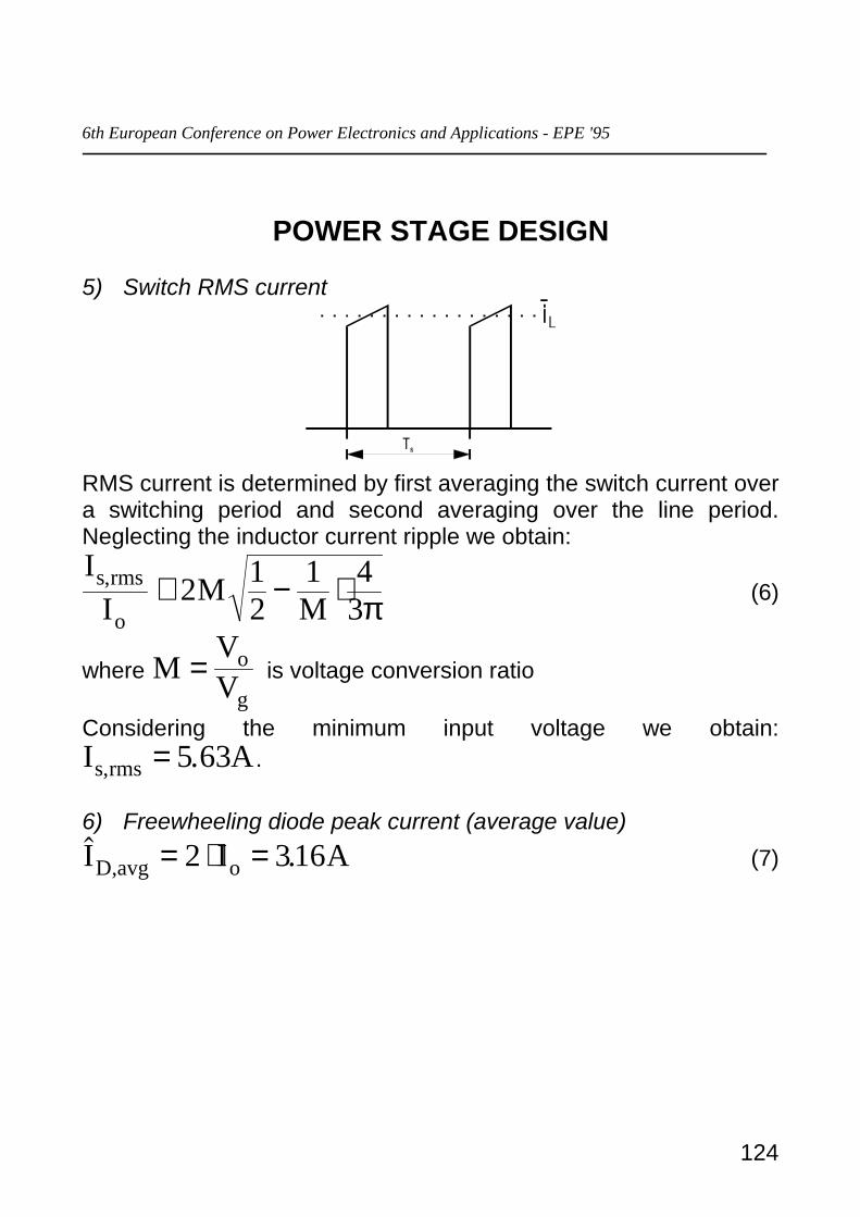
POWER STAGE DESIGN
5) Switch RMS current
RMS current is determined by first averaging the switch current overa switching period and second averaging over the line period.Neglecting the inductor current ripple we obtain:I
I M Ms rms
o
, ≅ − ⋅2 12
1 43π (6)
where MVV
o
g= is voltage conversion ratio
Considering the minimum input voltage we obtain:I As rms, .= 5 63 .
6) Freewheeling diode peak current (average value) .,I I AD avg o= ⋅ =2 316 (7)

6th European Conference on Power Electronics and Applications - EPE '95
125
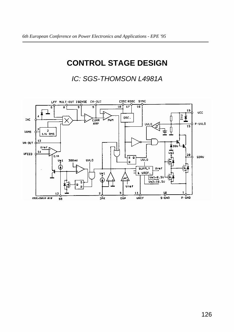
CONTROL STAGE DESIGN
IC: SGS-THOMSON L4981A
COMPONENT VALUES
Vcc = 18V R7 = 3.3 kΩ R13 = 18 kΩ C4 = 100 nFR2 = 150 kΩ R8 = 3.3 kΩ R14 = 5.6kΩ C5 = 1 nFR3 = 1 MΩ R9 = 47 kΩ C6 = 68 pFR4 = 560 kΩ R10 = 33 Ω C1 = 15 nF C7 = 10 µFR5 = 33 kΩ R11 = 33 kΩ C2 = 220 nF C8 = 1 nFR6 = 1.2 MΩ R12 = 1.5 MΩ C3 = 220 nF C9 = 10 µF
6th European Conference on Power Electronics and Applications - EPE '95
126
CONTROL STAGE DESIGN
IC: SGS-THOMSON L4981A
6th European Conference on Power Electronics and Applications - EPE '95
127
CONTROL STAGE DESIGN
1) Shunt resistance RS:
Choosing Rs = 0.054Ω the power loss is:
P RI
WR SL
S= ⋅ =
.2
2 2 65 (8)
2) Switching frequency:
C8 and R11 determine the switching frequency:
f C R hertzs = ⋅2 4
8 11
. , (9)
Choosing C8=1nF gives R11=33kΩ
3 Reference current IAC:
IVRAC
g=
6(10)
The suggested value for R6 is 1.2MΩ. Correspondingly, IAC isbetween 106µA at minimum line voltage and 306µA at maximumline voltage.

6th European Conference on Power Electronics and Applications - EPE '95
128
CONTROL STAGE DESIGN
4) Feedforward voltage VRMS:
R3, C3, R4, R5, C4 form a low pass filter which must give at pin 7 aDC voltage between 1.5V and 6.5V. Suggested values are:R3=1MΩ, R4=560kΩ, R5=33kΩ, C3=220nF, C4=100nF:
VR
R R R V V VRMS g g= + + ⋅ ⋅ = ⋅ = ÷5
3 4 5
2 1 68 4 85π α . . (11)
This low-pass filter must give a good attenuation at twice the linefrequency.
5) Peak current limiter:
We choose Ipk,lim=11A:
I ARRpk
S,lim = ⋅100 14µ (12)
from which R14=5.6kΩ.

6th European Conference on Power Electronics and Applications - EPE '95
129
CONTROL STAGE DESIGN
6) R7 and R8 values:
If the current error amplifier has enough gain at line frequency wehave:R I R IS L MULT OUT⋅ = ⋅ −7 (13)
where IMULT-OUT is the multiplier output current, which is relatedto the output voltage of the voltage error amplifier VA-OUT by:
I IV
VMULT OUT ACA OUT
RMS−
−= ⋅−1 28
2.
(14)
which is valid if pin 6 (VLFF) is connected to pin 11 (VREF).
Imposing that the maximum input current occurs with a voltageVA-OUT=5V, we obtain R7=R8=3.3kΩ.

6th European Conference on Power Electronics and Applications - EPE '95
130
CONTROL STAGE DESIGN
7) Over voltage protection:
+⋅=
13
12REFmax,o R
R1VV (15)
Choosing R12=1.5MΩ and R13=18kΩ gives Vo,max=425V.
8) Soft-start:
Connecting a capacitor between pin 12 and ground a ramp voltageis generated which causes the duty-cycle to vary from minimum tonominal value.
Suggested value: C9 = 10µF.
9) Feedback signal divider:
V VR
R RREF op
p p= ⋅ +
2
1 2(16)
Rp1=1MΩ e Rp2=12kΩ + 4.7kΩ trimmer.
As suggested a filter capacitor C7 = 10µF is connected between pin11 (VREF) and ground.
6th European Conference on Power Electronics and Applications - EPE '95
131
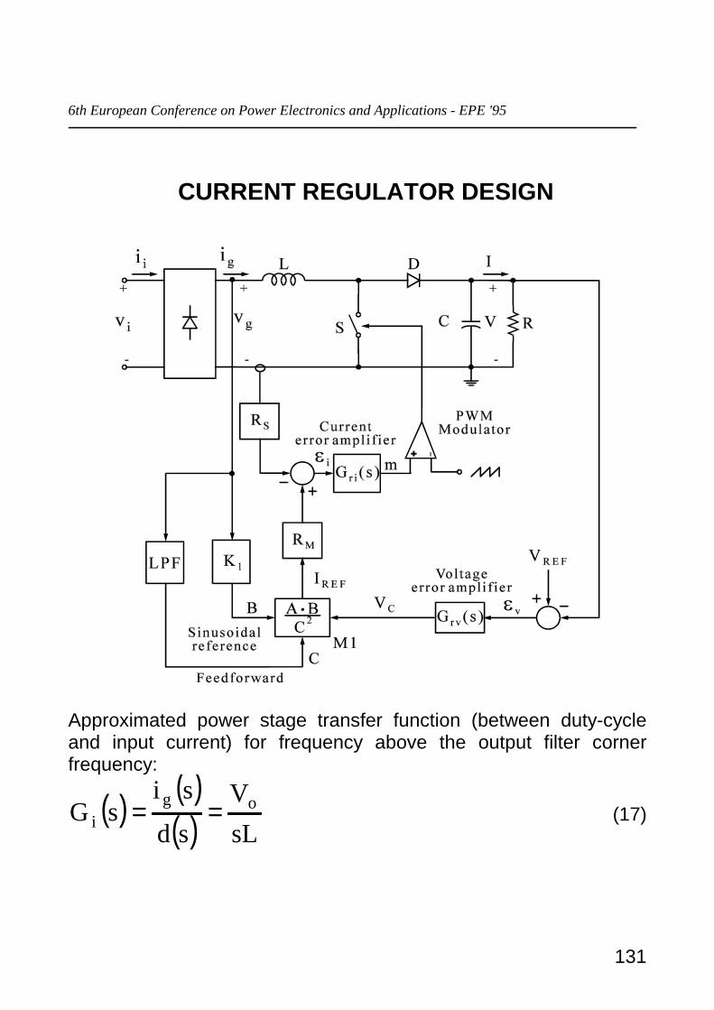
CURRENT REGULATOR DESIGN
Approximated power stage transfer function (between duty-cycleand input current) for frequency above the output filter cornerfrequency:
( ) ( )( ) sL
Vsd
sisG og
i == (17)
6th European Conference on Power Electronics and Applications - EPE '95
132
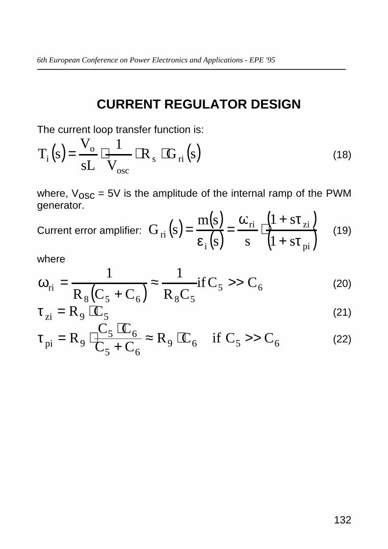
CURRENT REGULATOR DESIGN
The current loop transfer function is:
( ) ( )sGRV
1sLV
sT risosc
oi ⋅⋅⋅= (18)
where, Vosc = 5V is the amplitude of the internal ramp of the PWMgenerator.
Current error amplifier: ( ) ( )( )
( )( )pi
ziri
iri s1
s1ss
smsG
τ+τ+
⋅ω
=ε
= (19)
where
( ) 6558658
ri CCifCR
1CCR
1>>≈
+=ω (20)
τ zi R C= ⋅9 5 (21)
τ pi RC CC C R C if C C= ⋅
⋅+ ≈ ⋅ >>9
5 6
5 69 6 5 6 (22)

6th European Conference on Power Electronics and Applications - EPE '95
133
CURRENT REGULATOR DESIGN
If f f fzi c pi< < where fc is the crossover frequency, then:
( )8
9cri R
RjG ≈ω (23)
( )os
oscc
8
9ci VR
VLf2RR
1jT⋅
⋅⋅π==ω (24)
As far as the phase is concerned:
( )
180mff
arctgff
arctg9090jTpi
c
zi
cci −=
−
+−−=ω∠ ϕ (25)
where mϕ is the desired phase margin.
Given fc , the phase margin and choosing fs/2<fpi<fs so as toattenuate the high-frequency ripple R9, C5 and C6 values areobtained.
Example: fc = 15 kHz, fpi = 50 kHz and mϕ = 60° fzi = 3.5kHz,R9=47kΩ, C5=1nF, C6=68pF.

6th European Conference on Power Electronics and Applications - EPE '95
134
VOLTAGE REGULATOR DESIGN
Transfer function between control voltage and output voltage:
( ) ( )( ) p
pc
c
0v sCr1
rg
sVsV
sG+
⋅== (26)
where,
rr Zr Z g
Vk M r
VI M
VVp
o L
o Lc
g rmso
o
o
o
g rms=
⋅+ = ⋅ = =, , ,,
,(27)
ZL = RL = ro resistive loadZL = ¥ constant current loadZL = - RL constant power load
and k is defined by the relation:
IV
k vg rmsg rms
c,,= ⋅ (28)
In the L4981A controller, feedforward term VRMS eliminates thedependence of gain gc from input voltage.
6th European Conference on Power Electronics and Applications - EPE '95
135
VOLTAGE REGULATOR DESIGN
From eqs. (13-14) we can write (RM=R7):
2RMS,g
2OUTA
6
RMS,g
S
7
2RMS
OUTA
6
RMS,g
S
7OUTMULT
S
7RMS,g
V228.1V
RV
RR
V28.1V
RV
RR
IRR
I
α−
⋅⋅=
−⋅⋅=⋅=
−
−−
(29)
which corresponds to (28) if:
2RMS,g
2
543
5
7
S6 V
RRRR2
RR
R2k ⋅
++⋅
π⋅⋅= (30)

6th European Conference on Power Electronics and Applications - EPE '95
136
VOLTAGE REGULATOR DESIGN
The voltage regulator transfer function is:
( ) ( )( )
( )( )pv
zvrv
v
Crv s1
1ss
sVsG
τ+τ+
⋅ω
=ε
= (31)
where
ωrvp
p p
REF
o
RR R C C R
VV C R= + ⋅ + ⋅ ≈ ⋅ ⋅2
1 2 1 2 1 2 1
1 1 1 1 (C2>>C1) (32)
with R1=Rp1||Rp2τ zv R C= ⋅2 2 (33)
( ) 1212212pv CCseCRC//CR >>⋅≈⋅=τ (34)
Considering a crossover frequency higher than the power stagepole we have:
gj C
c
crv zvω ω τ⋅ =1 (35)
Choosing fc = 10÷20 Hz, fi<fpv<2fi and a suitable phase margin,the regulator parameters can be calculated.Example: fc = 20Hz, fpv = 70Hz and mϕ = 60° fzv = 5Hz,R2=150kΩ,C1=15nF, C2=220nF.

6th European Conference on Power Electronics and Applications - EPE '95
137
DESIGN OF A SEPIC PFC OPERATING INDCM
POWER STAGE SCHEME
PROTOTYPE PARAMETERS
Vg = 220 Vrms ± 20% V = 36 V P = 100W fs = 100 kHz
L2 = 74 µH C1 = 0.68 µF C2 = 10 µF n = 0.5

6th European Conference on Power Electronics and Applications - EPE '95
138
SEPIC MAIN EQUATIONS
1) Operation as dc/dc converter.
The voltage conversion ratio is:
M VV
II n D
Dg
g= = = ⋅ −1 (CCM)
M VV
II
DKg
g= = = (DCM)
where n=N2/N1 is transformer turns ratio, D is duty-cycle andparameter K is given by:
KL
RT LL L
L Le
se= = +
2 1 2
1 2, with
In the above equations Ts is the switching period and L2 is thetransformer magnetizing inductance.
Critical parameter:( )
( )
<>
+=
−=
DCMKKCCMKK
Mn1
nD1K
crit
crit22
2
crit
6th European Conference on Power Electronics and Applications - EPE '95
139
SEPIC MAIN EQUATIONS
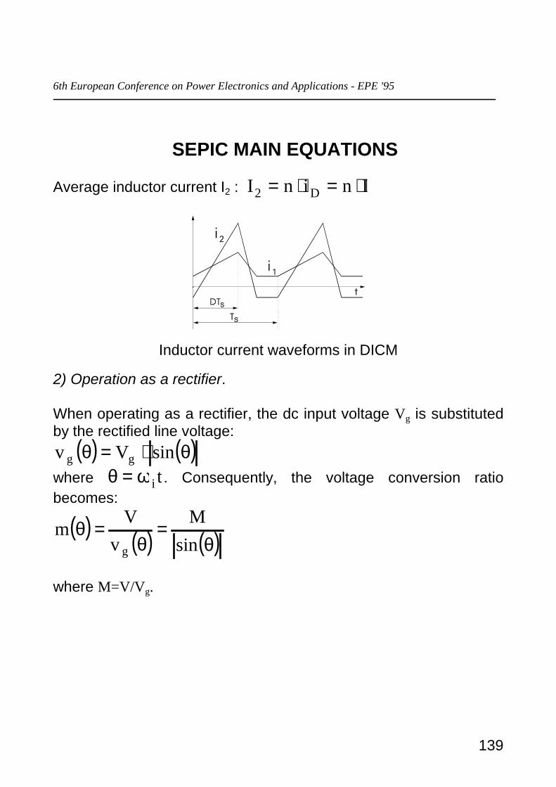
Average inductor current I2 : I n i n ID2 = ⋅ = ⋅
Inductor current waveforms in DICM
2) Operation as a rectifier.
When operating as a rectifier, the dc input voltage Vg is substitutedby the rectified line voltage:
( ) ( )θ⋅=θ sinVv ggwhere θ ω= i t . Consequently, the voltage conversion ratiobecomes:
( ) ( ) ( )θ=
θ=θ
sinM
vV
mg
where M=V/Vg.

6th European Conference on Power Electronics and Applications - EPE '95
140
SEPIC MAIN EQUATIONS
Under power factor correction conditions:( ) ( ) ( )θ⋅=θ⋅=θ 2
D2 sinI2nini
The apparent load r(q) seen at the secondary side of thetransformer is given by:
( ) ( ) ( )θ=
θ=θ
2D sin2
Ri
Vr
Thus the parameter k becomes function of angle q
( ) ( ) ( )s
ea
2a
s
e
RTL2
K,sinK2Tr
L2k =θ=
θ=θ
( ) ( )( )( )2
2
critsinnM
sink
θ⋅+
θ=θ
For the converter to operate in DCM the following condition must besatisfied:
( )( )2asinnM2
1K
θ⋅+<

6th European Conference on Power Electronics and Applications - EPE '95
141
SEPIC MAIN EQUATIONS
The average current drawn by the converter, at constant duty-cycleand switching frequency, is sinusoidal and in phase with the linevoltage and is given by
( ) ( ) ( )em
gg
e
s2
g R
vv
L2TD
iθ
=θ⋅=θ
where,
RL
D Teme
s
=2
2 is the emulated resistance.
The converter duty-cycle results:D M Ka= ⋅ 2

6th European Conference on Power Electronics and Applications - EPE '95
142
POWER STAGE DESIGN
INPUT DATA:
minimum and maximum input voltage peak value Vgmin,Vgmax;
output voltage V;
output power P;
switching frequency fs;
initial value for transformer turns ratio n.
6th European Conference on Power Electronics and Applications - EPE '95
143
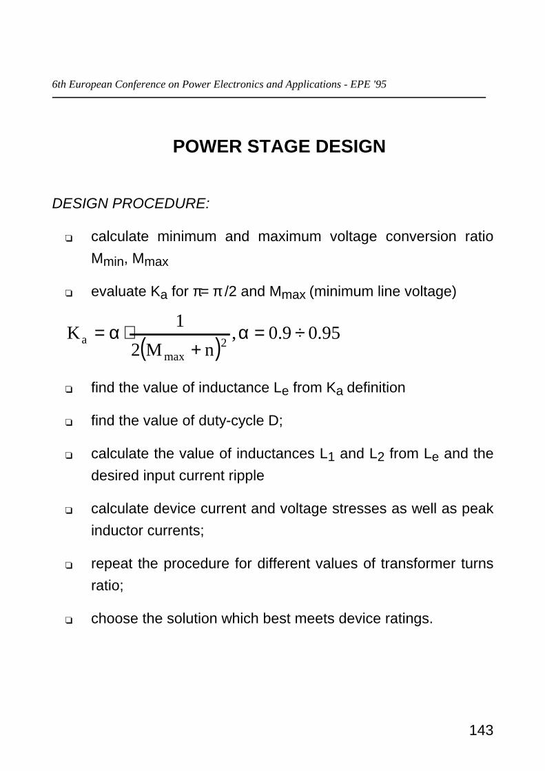
POWER STAGE DESIGN
DESIGN PROCEDURE:
calculate minimum and maximum voltage conversion ratioMmin, Mmax
evaluate Ka for π= π /2 and Mmax (minimum line voltage)
( )95.09.0,
nM21
K 2max
a ÷=α+
⋅α=
find the value of inductance Le from Ka definition
find the value of duty-cycle D;
calculate the value of inductances L1 and L2 from Le and thedesired input current ripple
calculate device current and voltage stresses as well as peakinductor currents;
repeat the procedure for different values of transformer turnsratio;
choose the solution which best meets device ratings.

6th European Conference on Power Electronics and Applications - EPE '95
144
POWER STAGE DESIGN
NOTE:
particular attention must be given to the selection of capacitor C1.Three constrains must be taken into account:
voltage u1 must follow the input voltage shape without distorsion
its voltage ripple must be as low as possible
C1 should not cause low-frequency oscillations with inductors L1
and L2.


