
8-Bit CMOS Microcontorller GMS97C2051/L2051
Hynix semiconductor 1
Features n Compatible with MCS-51TM Products n 2 Kbytes of programmable EPROM n 4.25V to 5.5V Operating Range (GMS97C2051) 2.70V to 3.6V Operating Range (GMS97L2051) n Version for 12MHz / 24 MHz Operating frequency (GMS97C2051) Only 12MHz Operating frequency (GMS97L2051) n Two-Level Program Memory Lock with encryption array n 128 bytes SRAM n 15 Programmable I/O Lines n Two 16-Bit Timer/Counters n Programmable serial USART n Five Interrupt Sources n Direct LED Drive Outputs n On-Chip Analog Comparator n Low Power Idle and Power Down Modes
Description The GMS97C2051/L2051 is a high-performance CMOS 8-bit microcontroller with 2Kbytes of programmable
EPROM. The device is compatible with the industry standard MCS-51TM instruction set and pinout. The Hynix
semiconductor GMS97C2051/L2051 is a powerful microcontroller which provides a highly flexible and cost
effective solution to many embedded control applications. The GMS97C2051/L2051 provides the following
standard features: 2Kbytes of EPROM, 128 bytes of RAM, 15 I/O lines, two 16-bit timer/counters, a five vec-
tor two-level interrupt architecture, a full duplex serial port, a precision analog comparator, on-chip oscillator
and clock circuitry. In addition, the GMS97C2051/L2051 supports two software selectable power saving modes.
The Idle Mode stops the CPU while allowing the RAM, timer/counters, serial port and interrupt system to con-
tinue functioning. The Power Down Mode saves the RAM contents but freezes the oscillator disabling all
other chip functions until the next hardware reset.
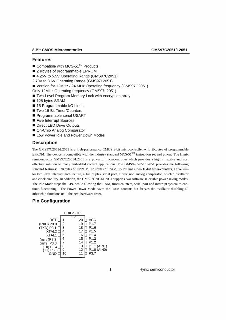
Pin Configuration
PDIP/SOP
(T0) P3.4
VCC P1.7 P1.6 P1.5 P1.4 P1.3 P1.2 P1.1 (AIN1) P1.0 (AIN0) P3.7
RST (RXD) P3.0 (TXD) P3.1
XTAL2 XTAL1
( INT1) P3.3
(T1) P3.5 GND
20 19 18 17 16 15 14 13 12 11
1 2 3 4 5 6 7 8 9 10
( INT0 )P3.2

GMS97C2051/L2051 8-Bit CMOS Microcontroller
Hynix semiconductor 2
Block Diagram
VCC
GND
P1.0-P1.7
RAM ADDR
REGISTER
RAM
STACK POINTER
PC INCREMENTER
PROGRAM COUNTER
ACC
EPROM
PROGRAM ADDRESS REGISTER
BUFFER
DPTR
TMP1 TMP2
PSW
B REGISTER
INTERRUPT, SERIAL PORT AND TIMER BLOCKS
OSC
PORT 3 LATCH
PORT 1 LATCH
TIMING AND
CONTROL
INSTRUCTION
REGISTER
+ _
PORT 1 DRIVERS PORT 3 DRIVERS
RST
P3.0-P3.5 P3.7
ANALOG COMPARATOR
ALU

8-Bit CMOS Microcontorller GMS97C2051/L2051
Hynix semiconductor 3
Pin Description
Vcc Supply voltage.
GND Ground.
Port 1 Port 1 is an 8-bit bidirectional I/O port. Port pins P1.2 to P1.7 provide internal pullups. P1.0 and P1.1 require external pullups. P1.0 and P1.1 also serve as the positive input (AIN0) and the negative input (AIN1), respectively, of the on-chip precision analog comparator. The Port 1 output buffers can sink 10mA and can drive LED displays directly. When 1s are written to Port1 pins, they can be used as inputs. When pins P1.2 to P1.7 are used as inputs and are externally pulled low, they will source current (IIL) because of the internal pullups. Port 1 also receives code data during EPROM pro-gramming and program verification.
Port3 Port 3 pins P3.0 to P3.5, P3.7 are seven bidirectional I/O pins with internal pullups. P3.6 is hard-wired as an input to the output of the on-chip comparator and is not accessible as a general purpose I/O pin. The Port 3 output buffers can sink 10mA. When 1s are writ-ten to Port 3 pins they are pulled high by the internal pullups and can be used as inputs. As inputs, Port 3 pins that are externally being pulled low will source current (IIL) because of the pullups. Port 3 also serves the functions of various special fea-ture of the GMS97C2051 as listed below:
Port Pin Alternate Functions
P3.0 P3.1 P3.2 P3.3 P3.4 P3.5
RXD ( serial input port ) TXD ( serial output port )
INT0 ( external interrupt 0 )
INT1( external interrupt 1 ) T0 ( timer 0 external input ) T1 ( timer 0 external input )
Port 3 also receives some control signals for EPROM programming and programming verification.
RST Reset input. All I/O pins are reset to 1s as soon as RST goes high. Holding the RST pin high for two machine cycles while the oscillator is running resets the device. This pin is also receives the 12.75V programming supply voltage ( Vpp ) during EPROM programming.
XTAL1 Input to the inverting oscillator amplifier and input to the internal clock operating circuit.
XTAL2 Output from the inverting oscillator amplifier.
Recommended Oscillator Circuit XTAL1 and XTAL2 are the input and output, respec-tively, of an inverting amplifier which can be config-ured for use as an on-chip oscillator, as shown in Fig-ure 1. To drive the device from an external clock source, XTAL2 should be left unconnected while XTAL1 is driven as shown in Figure 2.
Figure 1. Oscillator Connections
C 2
C 1
X T A L 2
X T A L 1
G N D
Notes: C1, C2 = 30pF¡ ¾ 10pF for Crystals ( include stray capacitance )
Figure 2. External Clock Drive Configuration
XTAL2
XTAL1
GND
EXTERNALOSCILLATOR
SIGNAL
NC

GMS97C2051/L2051 8-Bit CMOS Microcontroller
Hynix semiconductor 4
Special Function Registers A map of the on-chip memory area called the Special Function Register (SFR) space is shown in the Table1, Table 2 and Table 3. Note that not all of the addresses are occupied, and unoccupied addresses may not be implemented on the chip. Read accesses to these addresses will in gen-eral return random data, and write accesses will have an indeterminate effect.
User software should not write 1s to these unlisted locations, since they may be used in future products to invoke new features. In that case, the reset or inac-tive values of the new bits will always be 0.
Table 1. GMS97C2051/L2051 SFR Map and Reset Values
0F8H
0FFH
0F0H B
00000000
0F7H
0E8H
0EFH
0E0H ACC
00000000
0E7H
0D8H
0DFH
0D0H PSW
00000000
0D7H
0C8H
0CFH
0C0H
0C7H
0B8H IP
XXX00000
0BFH
0B0H P3
11111111
0B7H
0A8H IE
0XX00000
0AFH
0A0H
0A7H
98H SCON
00000000 SBUF
XXXXXXXX
9FH
90H P1
11111111
97H
88H TCON
00000000 TMOD
00000000 TL0
00000000 TL1
00000000 TH0
00000000 TH1
00000000
8FH
80H SP
00000111 DPL
00000000 DPH
00000000 PCON
0XXX0000 87H

8-Bit CMOS Microcontorller GMS97C2051/L2051
Hynix semiconductor 5
Table 2. Bit Assignment of SFRs
Address Register Bit7 Bit6 Bit5 Bit4 Bit3 Bit2 Bit1 Bit0
81H SP
82H DPL
83H DPH
87H PCON SMOD - - - GF1 GF0 PD IDLE
88H TCON TF1 TR1 TF0 TR0 IE1 IT1 IE0 IT0
89H TMOD GATE C / T M1 M0 GATE C / T M1 M0
8AH TL0
8BH TL1
8CH TH0
8DH TH1
90H P1
98H SCON SM0 SM1 SM2 REN TB8 RB8 TI RI
99H SBUF
A8H IE EA - - ES ET1 EX1 ET0 EX0
B0H P3
B8H IP - - - PS PT1 PX1 PT0 PX0
D0H PSW CY AC F0 RS1 RS0 OV F1 P
E0H ACC
F0H B
- : This Bit Location is reserved
Bit manipulation is available
Bit manipulation is not available

GMS97C2051/L2051 8-Bit CMOS Microcontroller
Hynix semiconductor 6
Table 3. SFR lists and their addresses
Symbol Name Address
* ACC * B
DPH DPL
* PSW SP
Accumulator B Register Data Pointer High Byte Data Pointer Low Byte Program Status Word Stack Pointer
E0H F0H
83H 82H
D0H 81H
* IE * IP
Interrupt Enable Control Interrupt Priority Control
A8H
B8H
* P1 * P3
Port 1 Port 3
90H
B0H
* SCON SBUF
Serial Control Serial Data Buffer
98H
99H
* TCON TH0 TH1 TL0 TL1
* TMOD
Timer/Counter Control Timer/Counter 0 High Bytes Timer/Counter 1 High Bytes Timer/Counter 0 Low Bytes Timer/Counter 1 Low Bytes Timer/Counter Mode Control
88H
8CH 8DH 8AH 8BH 89H
* = Bit addressable SFR
Timer/Counter 0 and 1The GMS97C2051/L2051 has two 16-bit Timer/ Counter register : Timer0 and Timer1 . As a Timer, the register is incremented every machine cycle. Thus, the register counts machine cycle. Since a machine cycle consists of 12 oscillator periods, the count rate is 1/12 of the oscillator frequency. As a counter, the register is incremented in response to a 1-to-0 transition at its corresponding external input pin P3.4/T0 and P3.5/T1. Since 2 machine
cycles are required to recognize a 1-to-0 transition, the maximum count rate is 1/24 of the oscillator frequency. External inputs P3.2/INT0 and 3.3/INT1 can be programmed to function as a gate to facilitate pulse width measurements. Timer/Counter 0 and 1 can be used in four operat-ing modes as listed in Table 4. Figure 3 illus-trates the input clock logic.
Table 4. Timer / Counter 0 and 1 Operating Modes
Mode Description TMOD
Gate C / T M1 M0
0 8-bit Timer/Counter with 5-bit prescaler × × 0 0
1 16-bit timer/counter × × 0 1
2 8-bit Auto-Reload Timer/Counter × × 1 0
3
(Timer 0) : TL0 is an 8-bit Timer/Counter controlled by the standard Timer 0 control bits, TH0 is an 8-bit Timer and is controlled by Timer 1 (Timer 1) : stop
×
×
1
1

8-Bit CMOS Microcontorller GMS97C2051/L2051
Hynix semiconductor 7
Figure 3. Time/Counter 0 and 1 Input Clock Logic
Serial Interface (USART) The serial port is full duplex, meaning it can trans-mit and receive simultaneously. And it can operate in four modes (one synchronous mode, three asyn-chronous mode) as illustrated in table 5. The pos-
The possible baud rates can be calculated using the formulas given in table 6.
Table 5. USART Operating Modes
Mode SCON Baud Rate Description SM0 SM1 0 0 0 fosc / 12
( fixed ) Shift Register : Serial data enters and exits through RXD. TXD outputs the shift clock. Eight data bits are transmitted / received, with the LSB first.
1 0 1 Set by Timer ( variable )
8-bit UART : Ten bits are transmitted through TXD, or received through RXD ¡ æ a start bit (0), 8 data bits (LSB first), and a stop bit (1)
2 1 0 fosc / 64 or fosc / 32 ( fixed )
9-bit UART : Eleven bits are transmitted through TXD, or received through RXD ¡ æ a start bit (0), 8 data bits (LSB first), a programmable ninth data bit , and a stop bit (1)
3 1 1 Set by Timer ( variable )
9-bit UART : The same as Mode 2 except the variable baud rate.
fosc ¡ À12
P3.4/T0 P3.5/T1
max fosc/24
TR 0/1
TCON
Gate
TMOD =1
¡ Ã1
&
0
1
fosc/12
Timer 0/1
Input Clock
Control
C/T
TMOD
P3.2/INT0
P3.3/INT1

GMS97C2051/L2051 8-Bit CMOS Microcontroller
Hynix semiconductor 8
Table 6. Formulas for calculating Baud rates
Baud Rate generated from
Serial Port Mode Baud Rate
Oscillator 0 2
fosc / 12 (2SMOD x fosc) / 64
Timer1 (Timer1 Mode2)
1 , 3 1 , 3
(2SMOD x Timer1 overflow rate) / 32 (2SMOD x fosc) / [32 x 12 x (256-TH1)]
Interrupt SystemThe GMS97C2051/L2051 provides 5 interrupt sources ( two external interrupts, two timer inter-rupts and serial port interrupt ) with two priority levels. Figure 4 gives a general overview of the interrupt sources and illustrates the request and control flags. A low-priority interrupt can itself be interrupted by a high-priority interrupt, but not by another low priority interrupt. A high-priority interrupt can-
not be interrupted by any other interrupt source. If two requests of different priority levels are re-ceived simultaneously, the request of higher priority is serviced. If requests of the same prior-ity level are received simultaneously, an internal polling sequence determines which request is ser-viced. Thus within each priority level there is a second priority structure determined by the polling sequence like Table 8.
Figure 4. Interrupt Request Sources
Timer 1 Overflow
ET1
IE.3
PT1
IP.3
TF1
TCON.7
IT0
TCON.0
¢¹
TCON.1
IE0
EX0
IE.0
PX0
IP.0
P3.2/
INT0
EA
IE.7
IT1
TCON.2
¢¹
TCON.3
IE1
EX1
IE.2
PX1
IP.2
P3.3/
INT1
TF0
TCON.5
Timer 0 Overflow
ET0
IE.1
PT0
IP.1
¡Ã1
R1
SCON.0USART
SCON.1
T1 ES
IE.4
PS
IP.4
High Priority
Low Priority

8-Bit CMOS Microcontorller GMS97C2051/L2051
Hynix semiconductor 9
Table 7. Interrupt Sources and their corresponding Interrupt Vectors
Interrupt Source Vector Address
External interrupt 0 Timer0
External Interrupt 1 Timer1
Serial Port Interrupt System Reset
IE0 TF0 IE1 TF1
RI + TI RST
0003H 000BH 0013H 001BH 0023H 0000H
Table 8. Interrupt Priority-Within-Level
Interrupt Source Priority
External interrupt 0 Timer0 interrupt
External Interrupt 1 Timer1 interrupt
Serial Port Interrupt
IE0 TF0 IE1 TF1
RI + TI
Highest
Lowest
Restrictions on Certain InstructionsThe GMS97C2051/L2051 is an economical and cost-effective member of Hynix semiconductor growing family of microcontrollers. It contains 2Kbytes of EPROM program memory. It is fully compatible with the MCS-51 architecture, and can be pro-grammed using the MCS-51 instruction set. How-ever, there are a few considerations one must keep in mind when utilizing certain instructions to program this device. 1. Branching instructions:
LCALL, LJMP, ACALL, AJMP, SJMP, JMP @A+DPTR These unconditional branching instructions will exe-cute correctly as long as the programmer keeps in mind that the destination branching address must fall within the physical boundaries of the program memory size (locations 00H to 7FFH for the GMS97C2051/L2051). Violating the physical space limits may cause unknown program behavior. CJNE [...], DJNZ [...], JB, JNB, JC, JNC, JBC, JZ, JNZ
With these conditional branching instructions the same rule above applies. Again, violating the memory boundaries may cause erratic execution. For applications involving interrupts the normal inter-rupt service routine address locations of the 80C51 family architecture have been preserved.
2. MOVX-related instructions, Data Memory:
The GMS97C2051/L2051 contains 128 bytes of inter-nal data memory. Thus, in the GMS97C2051/L2051 the stack depth is limited to 128 bytes, the amount of available RAM. External DATA memory access is not supported in this device, nor is external PRO-GRAM memory execution. Therefore, no MOVX [...] instructions should be included in the program. A typical 80C51 assembler will still assemble instruc-tions, even if they are written in violation of the re-strictions mentioned above. It is the responsibility of the controller user to know the physical features and limitations of the device being used and adjust the instructions used correspondingly.

GMS97C2051/L2051 8-Bit CMOS Microcontroller
Hynix semiconductor 10
Idle Mode In idle mode, the CPU puts itself to sleep while all the on-chip peripherals remain active. The mode is in-voked by software. The content of the on-chip RAM and all the special functions registers remain un-changed during this mode. The idle mode can be terminated by any enabled interrupt or by a hardware reset. P1.0 and P1.1 should be set to ‘ 0’ if no exter-nal pullups are used, or set to ‘ 1’ if external pullups are used. It should be noted that when idle is terminated by a hardware reset, the device normally resumes program execution, from where it left off, up to two machine cycles before the internal reset algorithm takes control. On-chip hardware inhibits access to internal RAM in this event, but access to the port pins is not inhibited. To eliminate the possibility of an unexpected write to a port pin when Idle is terminated by reset, the instruc-tion following one that invokes Idle should not be one that writes to a port pin or to external memory.
Power Down Mode GMS97C2051/L2051 have two power saving modes, Idle and Power Down. The bits PD and IDLE of the register PCON select the Power Down mode and the Idle mode, respectively. If 1s are written to PD and IDLE at the same time, PD takes precedence. Table 9 gives a general overview of the Power saving modes. In the Power Down mode of operation, VCC can be reduced to minimize power consumption. It must be ensured, however, that Vcc is not reduced before the Power Down mode is invoked, and that Vcc is restored to its normal operating level, before the Power Down mode is terminated. The reset signal that terminates the Power down mode also restarts the oscillator. The reset should not be activated before Vcc is re-stored to its normal operating level and must be held active long enough to allow the oscillator to restart and stabilize. ( similar to power-on reset ).
Table 9. Power Saving Modes Overview
Mode Ex. instruction to enter To terminate Remarks
Idle mode ORL PCON, #01H Enabled interrupt, Hardware Reset
- CPU is gated off - CPU status registers maintain their data. - Peripherals are active
Power-down Mode ORL PCON, #02H Hardware Reset - Oscillator stops - Contents of on-chip RAM and SFRs are maintained - Reset redefines all the SFRs but does not change the on-chip RAM
8-Bit CMOS Microcontorller GMS97C2051/L2051
Hynix semiconductor 11
Programming The EPROM The GMS97C2051/L2051 is programmed by using a modified Quick-Pulse ProgrammingTM algorithm. It differs from older methods in the value used for VPP (programming supply voltage) and in the width and number of the P3.2( PROG ) . The GMS97C2051/L2051 contains two signature bytes that can be read and used by an EPROM pro-gramming system to identify the device. The signature bytes identify the device as an manufactured by HME . Table 10 shows the logic levels for reading the signa-ture byte, and for programming the program memory, the encryption table, and the security bits. The circuit configuration and waveforms for quick-pulse pro-gramming are shown in Figures 5 and Figure 8. Figure 6 shows the circuit configuration for normal program memory verification. EPROM Programming and Verification Internal Address Counter : The GMS97C2051/L2051 contains an internal EPROM address counter which is always set to 07FFH on the rising edge of RST after setting P3.0 to ‘H’ and is advanced by applying continuous level transition to pin P3.0. Programming Algorithm : To program the GMS97C2051/L2051, the following sequence is recommended. 1. Power-up Sequence Apply power between VCC and GND pins with crystal oscillation. Set P3.0 to ‘H’. Set RST to GND. With all other pins floating, wait for greater than 10ms. 2. Set pin RST to ‘H’ and pin P3.2 to ‘H’. 3. Apply the appropriate combination of ‘H’ or ‘L’ logic levels to pins P3.3, P3.4, P3.5, P3.7 to select one of the programming operations shown in the EPROM Programming Modes. (Table 10). To program and verify the array 4. The P3.0 level is pulled ‘L’ and apply data for code byte at location 0000H to P1.0 to P1.7 5. Raise RST to 12.75V to enable programming. 6. The P3.2( PROG ) is pulsed low 10 times as shown in Figure 8. Each programming pulse is low for 100us(±10us) and high for a minimum of 10us. 7. To verify the programmed data, lower RST from
12.75V to logic ‘H’ level and set pins P3.3 to P3.7 to the appropriate levels. Output data can be read at the port P1 pins. At this time P3.0 should not be changed. 8. To program a byte at the next address location, P3.0 level transition is needed to advance the internal address counter. Apply new data to the port P1 pins. 9. Repeat step 5 through 8, changing data and advancing the address counter for the entire 2K bytes array. Program Verify : If lock bits LB1 and LB2 have not been programmed, code data can be read back via port P1 pins. 1. Set the internal address counter to 07FFH by bringing RST from ‘L’ to ‘H’ and reset the internal address counter to 0000H by bringing P3.0 from ‘H’ to ‘L’. 2. Apply the appropriate control signals for Read Code data to pins P3.3, P3.4, P3.5, P3.7 and read the output data at the port P1 pins. 3. The P3.0 level transition is taken to advance the internal address counter. 4. Read the next code data byte at the port P1 pins. 5. Repeat step 3 and 4 until the entire array is read.
Program Memory Lock Bits The two-level Program Lock system consists of 2 Lock bits and a 32-byte Encryption Array which are used to protect the program memory against software piracy.
Encryption Array : Within the EPROM array are 32 bytes of Encryption Array that are initially unprogrammed (all 1s). Every time that a byte is addressed during a verify, address lines are used to select a byte of the Encryption array. This byte is then exclusive-NORed (XNOR) with the code byte, creating an Encrypted Verify byte. The algorithm, with the array in the unprogrammed state (all 1s), will return the code in its original, un-modified form. It is recommended that whenever the Encryption Array is used, at least one of the Lock Bits be programmed as well.

GMS97C2051/L2051 8-Bit CMOS Microcontroller
Hynix semiconductor 12
Lock Bit Protection Modes
Program Lock Bits
LB1 LB2 Protection Type
1 U U No program lock features.
2 P U Further programming of the EPROM is disabled.
3 P P Same as mode 2, also verify is disabled.
Reading the Signature Bytes : The signature bytes are read by the same procedure as a normal verification of locations 000H and 001H, except that P3.5 and P3.7 need to be pulled to a logic low. Manufacturer ID: (00H) = E0H ( Indicates manufactured by HEI ) Device ID: (01H) = 26H ( Indicates GMS97C2051/L2051 )
U : unprogrammed, P : programmed
EPROM Programming Modes Table 10. EPROM Programming Modes
Mode RST P3.2/ PROG P3.3 P3.4 P3.5 P3.7
Read Signature 1 1 0 0 0 0
Program Code Data Vpp 0 1 1 1
Verify Code Data 1 1 0 0 1 1
Pgm encryption table Vpp 0 1 0 1
Pgm encryption bit1 Vpp 1 1 1 1
Pgm encryption bit Vpp 1 1 0 0
Notes: 1. '0' = Valid low, '1' = Valid high for that pin. 2. Vpp = 12.75 V ¡ ¾ 0.25 V 3. Vcc = 5 V ¡ ¾ 10 % during program-ming and verification.
4. P3.2/ PROG receives 10 programming pulses while Vpp is held at 12.75V. Each program- ming pulse is low for 100uS (¡ ¾10uS) and high for a minimum of 10uS.
8-Bit CMOS Microcontorller GMS97C2051/L2051
Hynix semiconductor 13
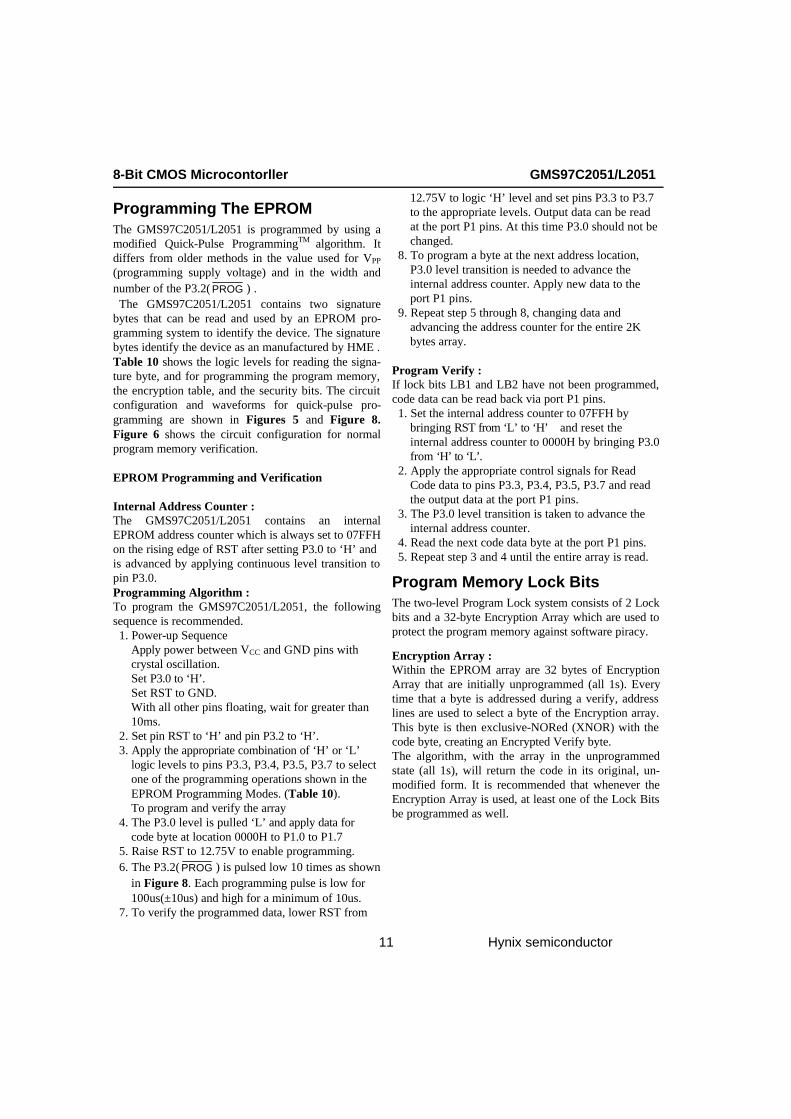
Figure 5. Programming the EPROM Memory
P3.0
P3.2
P3.3
P3.4
P3.5
P3.7
VCC
P1PGMDATA
VppXTAL2
GND
To IncrementAddress Counter
See EPROMProgramming
4~6MHz
Modes Tables
PROG
5VGMS97C1051
RST
XTAL1
Figure 6. Verifying the EPROM Memory
P3.0
P3.2
P3.3
P3.4
P3.5
P3.7
VCC
P1PGMDATA
5V
5V
XTAL2
GND
To IncrementAddress Counter
See EPROMProgramming
4~6MHz
Modes Tables
5VGMS97C1051
RST
XTAL1
EPROM Programming and Verification Characteristics Table 11. EPROM Programming and Verification Characteristics
Parameter Symbol Min Max Units
Programming Supply Voltage VPP 12.5 13.0 V
Programming Supply Current IPP 50 mA
Oscillator Frequency 1 / tCLCL 4 6 MHz
Address Setup to PROG Low tAVGL 48 tCLCL
Data Setup to PROG Low tDVGL 48 tCLCL
Data Hold after PROG tGHDX 48 tCLCL
P3.4 ( ENABLE ) High to VPP tEHSH 48 tCLCL
VPP Setup to PROG Low tSHGL 10 us
VPP Hold After PROG tGHSL 10 us
PROG Width tGLGH 90 110 us
PROG High to PROG Low tGHGL 10 us
P3.4 ( ENABLE ) Low to Data Valid tELQV 48 tCLCL
Data Float after P3.4 (ENABLE ) tEHQZ 0 48 tCLCL
TA= 21¡ É to 27¡ É, VCC = 5.0 ¡ ¾ 10%

GMS97C2051/L2051 8-Bit CMOS Microcontroller
Hynix semiconductor 14
EPROM Programming and Verification Waveforms Figure 7. EPROM Programming and Verification
DATA IN DATA OUT
Address (N+1)
Address (N)
tEHSH
tGHGL
VPPLOGIC 1
LOGIC 0
RST
(VPP)
P3.4
(ENABLE)
PORT1
P3.2
(PROG)
P3.0
tGHSL
tDVGL tGHDX
tGLGH
tAVGL
tSHGL
tELQV tEHQZ
Programming Verification
Figure 8. Programming Waveform
P3.2/ PROG
10 PULSES
100§ Á ± 10§ Á 10§ Á MIN
P3.2/ PROG
8-Bit CMOS Microcontorller GMS97C2051/L2051
Hynix semiconductor 15
Absolute Maximum Ratings
Ambient temperature under bias (TA.) ........................ - 40¡ É to + 85¡ É
Storage temperature (TST) ....... -65¡ É to + 150¡ É
Voltage on VCC pin with respect to Ground(VSS) .............-0.5V to 6.5V
Voltage on any pin with respect to Ground(VSS) .....-0.5V to VCC+0.5V
Input Current on any pin during overload condition............-10mA to +10mA
Absolute sum of all input current during overload condition...................... | 100 mA |
NOTE : Stresses above those listed under “Absolute Maximum Ratings” may cause permanent damage to the device. This is a stress rating only and functional operation of the device at these or any other conditions above those indicated in the operational sections of this specification is not implied. Exposure to absolute maximum rating conditions for longer periods may affect device reliability. During overload conditions (VIN > Vcc or VIN < Vss ) the voltage on Vcc pins with respect to ground (Vss) must not exceed the values defined by the absolute maximum ratings.

GMS97C2051/L2051 8-Bit CMOS Microcontroller
Hynix semiconductor 16
D.C. Characteristics (5V Version)
Vcc = 4.25V to 5.5V, Vss= 0V, TA= 0OC to 70OC for the GMS97C2051/C1051
Parameter Symbol Limit Values Unit Test
Min Max Condition
Input Low Voltage VIL -0.5 0.2Vcc-0.1 V
Input High Voltage (Except XTAL1, RST)
VIH 0.5Vcc-0.1 Vcc+0.5 V
Input High Voltage (XTAL1, RST)
VIH1 0.7Vcc Vcc+0.5 V
Output Low Voltage (ports 1,3)
VOL 0.45 V IOL=10mA,Vcc=5V
Output High Voltage (ports 1,3)
VOH 2.4 0.75Vcc 0.9Vcc
V IOH= -80uA, Vcc=5V±10% IOH= -30uA IOH= -12uA
Logical 0 Input Current (ports 1,3)
IIL -50 uA VIN=0.45V
Logical 1-to-0 Transition Current (ports 1,3)
ITL -750 uA VIN=2V
Input Leakage Current (Port P1.0, P1.1)
ILI ±1uA uA 0<VIN<Vcc
Comparator Input Offset Voltage
VOS 200 mV Vcc=5V
Comparator Input
Common Mode Voltage
VCM 0 Vcc V
Pin Capacitance CIO 10 pF Test Freq.=1MHz, TA=25 OC
Power supply current: Active mode, 12Mhz Idle mode, 12Mhz Active mode, 24Mhz Idle mode, 24Mhz Power Down mode
Icc
Iccidle Icc
Iccidle Ipd
20 12 30 15 100
mA mA mA mA uA
Vcc=5.0V
Vcc=5.0V, P1.0&P1.1=0 or Vcc
Vcc=5.0V
Vcc=5.0V, P1.0&P1.1=0 or Vcc
Vcc=5.0V, P1.0&P1.1=0 or Vcc
8-Bit CMOS Microcontorller GMS97C2051/L2051
Hynix semiconductor 17
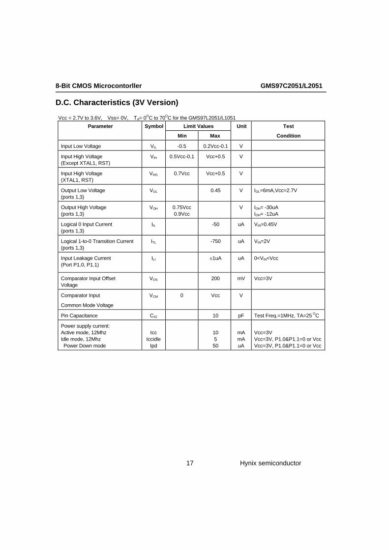
D.C. Characteristics (3V Version)
Vcc = 2.7V to 3.6V, Vss= 0V, TA= 0OC to 70OC for the GMS97L2051/L1051
Parameter Symbol Limit Values Unit Test
Min Max Condition
Input Low Voltage VIL -0.5 0.2Vcc-0.1 V
Input High Voltage (Except XTAL1, RST)
VIH 0.5Vcc-0.1 Vcc+0.5 V
Input High Voltage (XTAL1, RST)
VIH1 0.7Vcc Vcc+0.5 V
Output Low Voltage (ports 1,3)
VOL 0.45 V IOL=6mA,Vcc=2.7V
Output High Voltage (ports 1,3)
VOH 0.75Vcc 0.9Vcc
V IOH= -30uA IOH= -12uA
Logical 0 Input Current (ports 1,3)
IIL -50 uA VIN=0.45V
Logical 1-to-0 Transition Current (ports 1,3)
ITL -750 uA VIN=2V
Input Leakage Current (Port P1.0, P1.1)
ILI ±1uA uA 0<VIN<Vcc
Comparator Input Offset Voltage
VOS 200 mV Vcc=3V
Comparator Input
Common Mode Voltage
VCM 0 Vcc V
Pin Capacitance CIO 10 pF Test Freq.=1MHz, TA=25 OC
Power supply current: Active mode, 12Mhz Idle mode, 12Mhz Power Down mode
Icc
Iccidle Ipd
10 5 50
mA mA uA
Vcc=3V Vcc=3V, P1.0&P1.1=0 or Vcc Vcc=3V, P1.0&P1.1=0 or Vcc

GMS97C2051/L2051 8-Bit CMOS Microcontroller
Hynix semiconductor 18
External Clock drive waveforms
tCHCX
tCLCL
tCLCX
tCHCX tCLCH
0.7 VCC
0.2 VCC - 0.1V
0.45V
VCC - 0.5 V
tCHCL
External Clock Drive
Symbol Parameter GMS97L2051/L1051 GMS97C2051/C1051
Min Max Min Max
Units
1/tCLCL Oscillator Frequency 0 12 0 24 MHz
tCLCL Clock Period 83.3 41.6 ns
tCHCX High Time 30 15 ns
tCLCX Low Time 30 15 ns
tCLCH Rise Time - 20 - 20 ns
tCHCL Fall Time - 20 - 20 ns
AC Testing Input/Output Waveforms(1)
VCC - 0.5V
0.45V
0.2VCC + 0.9V
TEST POINTS
0.2VCC - 0.1V
Note: 1. AC Inputs during testing are driven at VCC - 0.5V for a logic 1 and 0.45V for a logic 0. Timing measurements are made at VIH min. for a logic 1 and VIL max. for a logic 0.
Float Waveforms(1)
VLOAD + 0.1V
VLOAD
VLOAD - 0.1V
VOL + 0.1V
VOL + 0.1V
Timing Reference
Points
Note: 1. For timing purposes, a port pin is no longer floating when a 100mV change from load voltage occurs. A port pin begins to float when a 100mV change from the loaded VOH/VOL level occurs.
8-Bit CMOS Microcontorller GMS97C2051/L2051
Hynix semiconductor 19
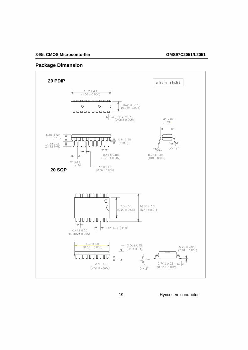
Package Dimension
20 PDIP
20 SOP
unit : mm ( inch )

GMS97C2051/L2051 8-Bit CMOS Microcontroller
Hynix semiconductor 20
Ordering Information
Speed ( MHz) Power Supply Ordering Code Package Operation Range
12 2.7V to 3.6V GMS97L2051 20 PDIP
GMS97L2051-D 20 SOP
4.25V to 5.5V GMS97C2051 20 PDIP Commercial
GMS97C2051-D 20 SOP (0¡ É to 70¡ É)
24 4.25V to 5.5V GMS97C2051-24 20 PDIP
GMS97C2051-24D 20 SOP
Package Type
20 PDIP 20 Lead, 0.300¡ ÈWide, Plastic Dual Inline Package (PDIP)
20 SOP 20 Lead, 0.300¡ ÈWide, Plastic Gull Wing Small Outline (SOP)
8-Bit CMOS Microcontorller GMS97C1051/L1051
Hynix semiconductor 21
Features n Compatible with MCS-51TM Products n 1 Kbytes of programmable EPROM n 4.25V to 5.5V Operating Range (GMS97C1051) 2.70V to 3.6V Operating Range (GMS97L1051) n Version for 12MHz / 24 MHz Operating frequency (GMS97C1051) Only 12MHz Operating frequency (GMS97L1051) n Two-Level Program Memory Lock with encryption array n 64 bytes SRAM n 15 Programmable I/O Lines n One 16-Bit Timer/Counter n Three Interrupt Sources n Direct LED Drive Outputs n On-Chip Analog Comparator n Low Power Idle and Power Down Modes
Description The GMS97C1051/L1051 is a high-performance CMOS 8-bit microcontroller with 1Kbytes of programmable
EPROM. The device is compatible with the industry standard MCS-51TM instruction set and pinout. The
Hynix semiconductor GMS97C1051/L1051 is a powerful microcontroller which provides a highly flexible and
cost effective solution to many embedded control applications. The GMS97C1051/L1051 provides the follow-
ing standard features: 1Kbytes of EPROM, 64 bytes of RAM, 15 I/O lines, 16-bit timer/counter, a three vector
two-level interrupt architecture, a precision analog comparator, on-chip oscillator and clock circuitry. In addi-
tion, the GMS97C1051/L1051 supports two software selectable power saving modes. The Idle Mode stops the
CPU while allowing the RAM, timer/counters, serial port and interrupt system to continue functioning. The
Power Down Mode saves the RAM contents but freezes the oscillator disabling all other chip functions until the
next hardware reset.
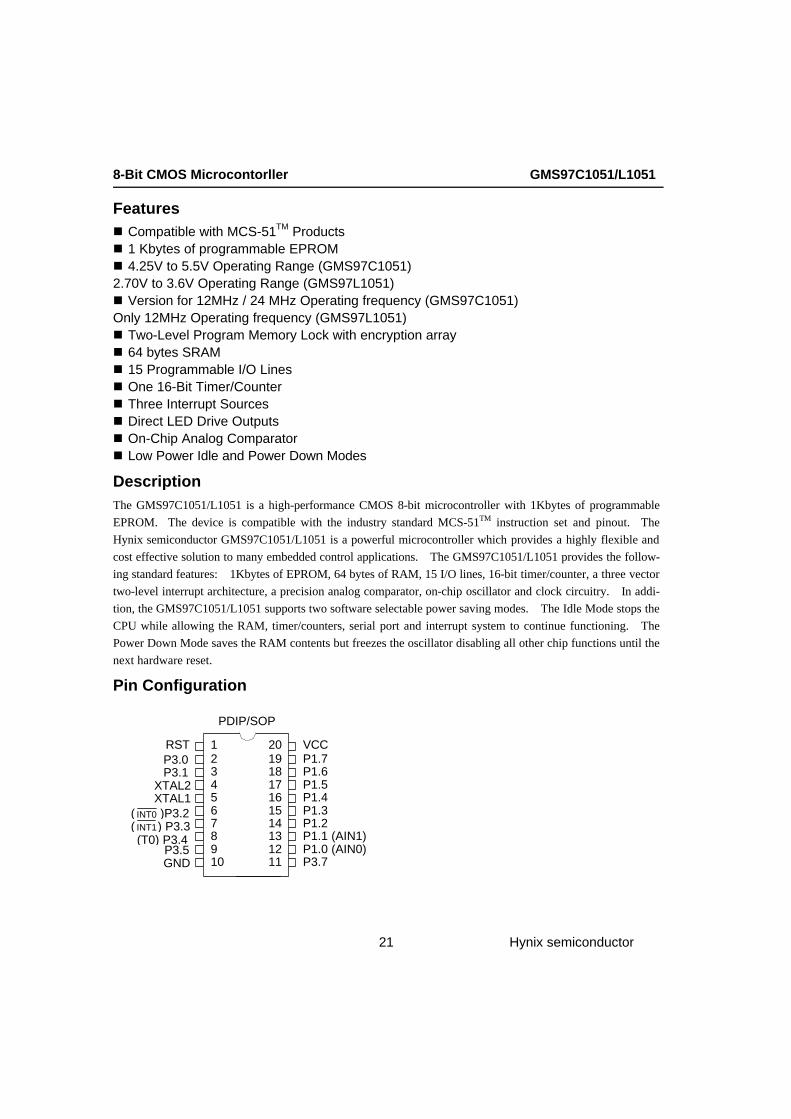
Pin Configuration
(T0) P3.4
VCC P1.7 P1.6 P1.5 P1.4 P1.3 P1.2 P1.1 (AIN1) P1.0 (AIN0) P3.7
RST P3.0 P3.1
XTAL2 XTAL1
( INT1) P3.3
P3.5 GND
20 19 18 17 16 15 14 13 12 11
1 2 3 4 5 6 7 8 9 10
PDIP/SOP
( INT0 )P3.2

GMS97C1051/L1051 8-Bit CMOS Microcontroller
Hynix semiconductor 22
Block Diagram
VCC
GND
P1.0-P1.7
RAM ADDR
REGISTER
RAM
STACK POINTER
PC INCREMENTER
PROGRAM COUNTER
ACC
EPROM
PROGRAM ADDRESS REGISTER
BUFFER
DPTR
TMP1 TMP2
PSW
B REGISTER
INTERRUPT , TIMER BLOCKS
OSC
PORT 3 LATCH
PORT 1 LATCH
TIMING AND
CONTROL
INSTRUCTION
REGISTER
+ _
PORT 1 DRIVERS PORT 3 DRIVERS
RST
P3.0-P3.5 P3.7
ANALOG COMPARATOR
ALU
8-Bit CMOS Microcontorller GMS97C1051/L1051
Hynix semiconductor 23
Pin Description
Vcc Supply voltage.
GND Ground.
Port 1 Port 1 is an 8-bit bidirectional I/O port. Port pins P1.2 to P1.7 provide internal pullups. P1.0 and P1.1 require external pullups. P1.0 and P1.1 also serve as the positive input (AIN0) and the negative input (AIN1), respectively, of the on-chip precision analog comparator. The Port 1 output buffers can sink 10mA and can drive LED displays directly. When 1s are written to Port1 pins, they can be used as inputs. When pins P1.2 to P1.7 are used as inputs and are externally pulled low, they will source current (IIL) because of the internal pullups. Port 1 also receives code data during EPROM pro-gramming and program verification.
Port3 Port 3 pins P3.0 to P3.5, P3.7 are seven bidirectional I/O pins with internal pullups. P3.6 is hard-wired as an input to the output of the on-chip comparator and is not accessible as a general purpose I/O pin. The Port 3 output buffers can sink 10mA. When 1s are writ-ten to Port 3 pins they are pulled high by the internal pullups and can be used as inputs. As inputs, Port 3 pins that are externally being pulled low will source current (IIL) because of the pullups. Port 3 also serves the functions of various special fea-ture of the GMS97C1051/L1051 as listed below:
Port Pin Alternate Functions
P3.2
P3.3
P3.4
INT0 (external interrupt 0)
INT1 (external interrupt 1)
T0 (timer 0 external input)
Port 3 also receives some control signals for EPROM programming and programming verification.
RST Reset input. All I/O pins are reset to 1s as soon as RST goes high. Holding the RST pin high for two machine cycles while the oscillator is running resets the device. This pin is also receives the 12.75V programming supply voltage ( Vpp ) during EPROM programming.
XTAL1 Input to the inverting oscillator amplifier and input to the internal clock operating circuit.
XTAL2 Output from the inverting oscillator amplifier.
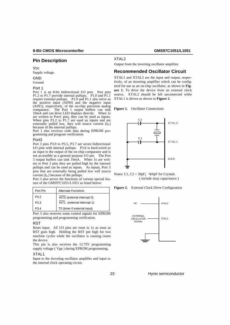
Recommended Oscillator Circuit XTAL1 and XTAL2 are the input and output, respec-tively, of an inverting amplifier which can be config-ured for use as an on-chip oscillator, as shown in Fig-ure 1. To drive the device from an external clock source, XTAL2 should be left unconnected while XTAL1 is driven as shown in Figure 2.
Figure 1. Oscillator Connections
C 2
C 1
X T A L 2
X T A L 1
G N D
Notes: C1, C2 = 30pF¡ ¾ 10pF for Crystals ( include stray capacitance )
Figure 2. External Clock Drive Configuration
GND
EXTERNALOSCILLATOR
SIGNAL
NC XTAL2
XTAL1

GMS97C1051/L1051 8-Bit CMOS Microcontroller
Hynix semiconductor 24
Special Function Registers A map of the on-chip memory area called the Special Function Register (SFR) space is shown in the Table1, Table 2 and Table 3. Note that not all of the addresses are occupied, and unoccupied addresses may not be implemented on the chip. Read accesses to these addresses will in gen-eral return random data, and write accesses will have an indeterminate effect.
User software should not write 1s to these unlisted locations, since they may be used in future products to invoke new features. In that case, the reset or inac-tive values of the new bits will always be 0.
Table 1. GMS97C1051/L1051 SFR Map and Reset Values
0F8H
0FFH
0F0H B
00000000
0F7H
0E8H
0EFH
0E0H ACC
00000000
0E7H
0D8H
0DFH
0D0H PSW
00000000
0D7H
0C8H
0CFH
0C0H
0C7H
0B8H IP
XXX00000
0BFH
0B0H P3
11111111
0B7H
0A8H IE
0XX00000
0AFH
0A0H
0A7H
98H
9FH
90H P1
11111111
97H
88H TCON
00000000 TMOD
00000000 TL0
00000000 TH0
00000000
8FH
80H SP
00000111 DPL
00000000 DPH
00000000 PCON
0XXX0000 87H
8-Bit CMOS Microcontorller GMS97C1051/L1051
Hynix semiconductor 25
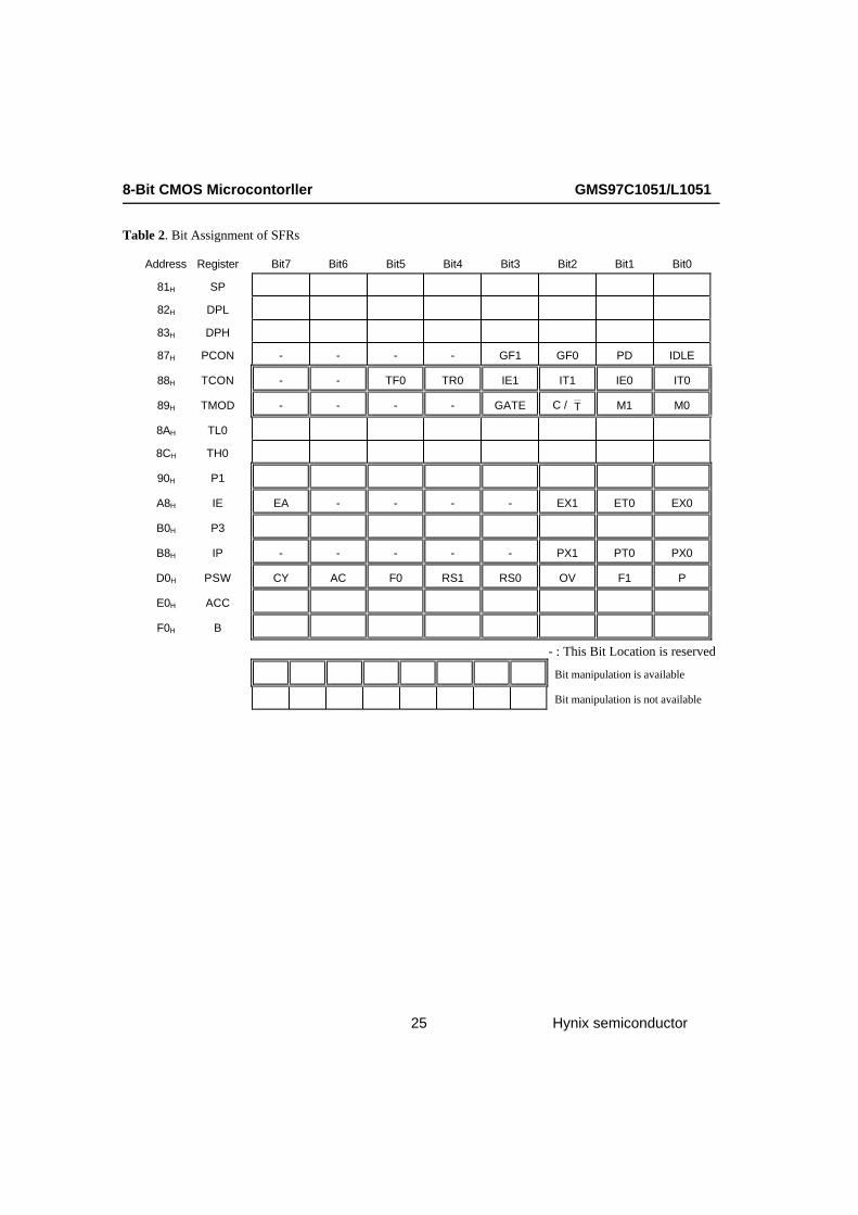
Table 2. Bit Assignment of SFRs
Address Register Bit7 Bit6 Bit5 Bit4 Bit3 Bit2 Bit1 Bit0
81H SP
82H DPL
83H DPH
87H PCON - - - - GF1 GF0 PD IDLE
88H TCON - - TF0 TR0 IE1 IT1 IE0 IT0
89H TMOD - - - - GATE C / T M1 M0
8AH TL0
8CH TH0
90H P1
A8H IE EA - - - - EX1 ET0 EX0
B0H P3
B8H IP - - - - - PX1 PT0 PX0
D0H PSW CY AC F0 RS1 RS0 OV F1 P
E0H ACC
F0H B
- : This Bit Location is reserved
Bit manipulation is available
Bit manipulation is not available

GMS97C1051/L1051 8-Bit CMOS Microcontroller
Hynix semiconductor 26
Table 3. SFR lists and their addresses
Symbol Name Address
* ACC * B
DPH DPL
* PSW SP
Accumulator B Register Data Pointer High Byte Data Pointer Low Byte Program Status Word Stack Pointer
E0H F0H
83H 82H
D0H 81H
* IE * IP
Interrupt Enable Control Interrupt Priority Control
A8H
B8H
* P1 * P3
Port 1 Port 3
90H
B0H
* TCON TH0 TL0
* TMOD
Timer/Counter Control Timer/Counter 0 High Bytes Timer/Counter 0 Low Bytes Timer/Counter Mode Control
88H
8CH 8AH 89H
* = Bit addressable SFR
Timer/Counter 0 The GMS97C1051/L1051 has one 16-bit Timer/ Counter register : Timer0 . As a Timer, the register is incremented every machine cycle. Thus, the register counts machine cycle. Since a machine cycle consists of 12 oscillator periods, the count rate is 1/12 of the oscillator frequency. As a counter, the register is incremented in response to a 1-to-0 transition at its corresponding external
input pin P3.4/T0. Since 2 machine cycles are required to recognize a 1-to-0 transition, the maximum count rate is 1/24 of the oscillator fre-quency. External inputs P3.2/INT0 and 3.3/INT1 can be programmed to function as a gate to facili-tate pulse width measurements. Timer/Counter 0 can be used in four operating modes as listed in Table 4. Figure 3 illustrates the input clock logic.
Table 4. Timer / Counter 0 Operating Modes
Mode Description TMOD
Gate C/T M1 M0
0 8-bit Timer/Counter with 5-bit prescaler × × 0 0
1 16-bit timer/counter × × 0 1
2 8-bit Auto-Reload Timer/Counter × × 1 0
3
(Timer 0) TL0 is an 8-bit Timer/Counter controlled by the standard Timer 0 control bits, TH0 is an 8-bit Timer
×
×
1
1
8-Bit CMOS Microcontorller GMS97C1051/L1051
Hynix semiconductor 27
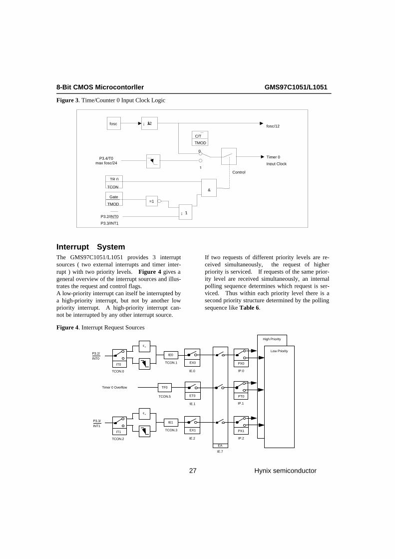
Figure 3. Time/Counter 0 Input Clock Logic
Interrupt SystemThe GMS97C1051/L1051 provides 3 interrupt sources ( two external interrupts and timer inter-rupt ) with two priority levels. Figure 4 gives a general overview of the interrupt sources and illus-trates the request and control flags. A low-priority interrupt can itself be interrupted by a high-priority interrupt, but not by another low priority interrupt. A high-priority interrupt can-not be interrupted by any other interrupt source.
If two requests of different priority levels are re-ceived simultaneously, the request of higher priority is serviced. If requests of the same prior-ity level are received simultaneously, an internal polling sequence determines which request is ser-viced. Thus within each priority level there is a second priority structure determined by the polling sequence like Table 6.
Figure 4. Interrupt Request Sources
IT0
TCON.0
¢¹
TCON.1
IE0
EX0
IE.0
PX0
IP.0
P3.2/
INT0
EA
IE.7
IT1
TCON.2
¢¹
TCON.3
IE1
EX1
IE.2
PX1
IP.2
P3.3/
INT1
TF0
TCON.5
Timer 0 Overflow
ET0
IE.1
PT0
IP.1
High Priority
Low Priority
fosc ¡ À12
P3.4/T0 max fosc/24
TR 0
TCON
Gate
TMOD =1
¡ Ã1
&
0
1
fosc/12
Timer 0
Input Clock
Control
C/T
TMOD
P3.2/INT0
P3.3/INT1
GMS97C1051/L1051 8-Bit CMOS Microcontroller
Hynix semiconductor 28
Table 5. Interrupt Sources and their corresponding Interrupt Vectors
Interrupt Source Vector Address
External interrupt 0 Timer0
External Interrupt 1 System Reset
IE0 TF0 IE1 RST
0003H 000BH 0013H 0000H
Table 6. Interrupt Priority-Within-Level
Interrupt Source Priority
External interrupt 0 Timer0 interrupt
External Interrupt 1
IE0 TF0 IE1
Highest
Lowest
Restrictions on Certain InstructionsThe GMS97C1051/L1051 is an economical and cost-effective member of Hynix semiconductor growing family of microcontrollers. It contains 1Kbytes of EPROM program memory. It is fully compatible with the MCS-51 architecture, and can be pro-grammed using the MCS-51 instruction set. How-ever, there are a few considerations one must keep in mind when utilizing certain instructions to program this device. 1. Branching instructions:
LCALL, LJMP, ACALL, AJMP, SJMP, JMP @A+DPTR These unconditional branching instructions will exe-cute correctly as long as the programmer keeps in mind that the destination branching address must fall within the physical boundaries of the program memory size (locations 00H to 3FFH for the GMS97C1051/L1051). Violating the physical space limits may cause unknown program behavior. CJNE [...], DJNZ [...], JB, JNB, JC, JNC, JBC, JZ, JNZ
With these conditional branching instructions the same rule above applies. Again, violating the memory boundaries may cause erratic execution. For applications involving interrupts the normal inter-rupt service routine address locations of the 80C51 family architecture have been preserved.
2. MOVX-related instructions, Data Memory:
The GMS97C1051/L1051 contains 64 bytes of inter-nal data memory. Thus, in the GMS97C1051/L1051 the stack depth is limited to 64 bytes, the amount of available RAM. External DATA memory access is not supported in this device, nor is external PRO-GRAM memory execution. Therefore, no MOVX [...] instructions should be included in the program. A typical 80C51 assembler will still assemble instruc-tions, even if they are written in violation of the re-strictions mentioned above. It is the responsibility of the controller user to know the physical features and limitations of the device being used and adjust the instructions used correspondingly.

8-Bit CMOS Microcontorller GMS97C1051/L1051
Hynix semiconductor 29
Idle Mode In idle mode, the CPU puts itself to sleep while all the on-chip peripherals remain active. The mode is in-voked by software. The content of the on-chip RAM and all the special functions registers remain un-changed during this mode. The idle mode can be terminated by any enabled interrupt or by a hardware reset. P1.0 and P1.1 should be set to ‘ 0’ if no exter-nal pullups are used, or set to ‘ 1’ if external pullups are used. It should be noted that when idle is terminated by a hardware reset, the device normally resumes program execution, from where it left off, up to two machine cycles before the internal reset algorithm takes control. On-chip hardware inhibits access to internal RAM in this event, but access to the port pins is not inhibited. To eliminate the possibility of an unexpected write to a port pin when Idle is terminated by reset, the instruc-tion following one that invokes Idle should not be one that writes to a port pin or to external memory.
Power Down Mode GMS97C1051/L1051 have two power saving modes, Idle and Power Down. The bits PD and IDLE of the register PCON select the Power Down mode and the Idle mode, respectively. If 1s are written to PD and IDLE at the same time, PD takes precedence. Table 7 gives a general overview of the Power saving modes. In the Power Down mode of operation, VCC can be reduced to minimize power consumption. It must be ensured, however, that Vcc is not reduced before the Power Down mode is invoked, and that Vcc is restored to its normal operating level, before the Power Down mode is terminated. The reset signal that terminates the Power down mode also restarts the oscillator. The reset should not be activated before Vcc is re-stored to its normal operating level and must be held active long enough to allow the oscillator to restart and stabilize. ( similar to power-on reset ).
Table 7. Power Saving Modes Overview
Mode Ex. instruction to enter To terminate Remarks
Idle mode ORL PCON, #01H Enabled interrupt, Hardware Reset
- CPU is gated off - CPU status registers maintain their data. - Peripherals are active
Power-down Mode ORL PCON, #02H Hardware Reset - Oscillator stops - Contents of on-chip RAM and SFRs are maintained - Reset redefines all the SFRs but does not change the on-chip RAM

GMS97C1051/L1051 8-Bit CMOS Microcontroller
Hynix semiconductor 30
Programming The EPROM The GMS97C1051/L1051 is programmed by using a modified Quick-Pulse ProgrammingTM algorithm. It differs from older methods in the value used for VPP (programming supply voltage) and in the width and number of the P3.2( PROG ) . The GMS97C1051/L1051 contains two signature bytes that can be read and used by an EPROM pro-gramming system to identify the device. The signature bytes identify the device as an manufactured by HME. Table 8 shows the logic levels for reading the signa-ture byte, and for programming the program memory, the encryption table, and the security bits. The circuit configuration and waveforms for quick-pulse pro-gramming are shown in Figures 5 and Figure 8. Figure 6 shows the circuit configuration for normal program memory verification. EPROM Programming and Verification Internal Address Counter : The GMS97C1051/L1051 contains an internal EPROM address counter which is always set to 03FFH on the rising edge of RST after setting P3.0 to ‘H’ and is advanced by applying continuous level transition to pin P3.0. Programming Algorithm : To program the GMS97C1051/L1051, the following sequence is recommended. 1. Power-up Sequence Apply power between VCC and GND pins with crystal oscillation. Set P3.0 to ‘H’. Set RST to GND. With all other pins floating, wait for greater than 10ms. 2. Set pin RST to ‘H’ and pin P3.2 to ‘H’. 3. Apply the appropriate combination of ‘H’ or ‘L’ logic levels to pins P3.3, P3.4, P3.5, P3.7 to select one of the programming operations shown in the EPROM Programming Modes. (Table 8). To program and verify the array 4. The P3.0 level is pulled ‘L’ and apply data for code byte at location 0000H to P1.0 to P1.7 5. Raise RST to 12.75V to enable programming. 6. The P3.2( PROG ) is pulsed low 10 times as shown in Figure 8. Each programming pulse is low for 100us(±10us) and high for a minimum of 10us. 7. To verify the programmed data, lower RST from
12.75V to logic ‘H’ level and set pins P3.3 to P3.7 to the appropriate levels. Output data can be read at the port P1 pins. At this time P3.0 should not be changed. 8. To program a byte at the next address location, P3.0 level transition is needed to advance the internal address counter. Apply new data to the port P1 pins. 9. Repeat step 5 through 8, changing data and advancing the address counter for the entire 1K bytes array. Program Verify : If lock bits LB1 and LB2 have not been programmed, code data can be read back via port P1 pins. 1. Set the internal address counter to 03FFH by bringing RST from ‘L’ to ‘H’ and reset the internal address counter to 0000H by bringing P3.0 from ‘H’ to ‘L’. 2. Apply the appropriate control signals for Read Code data to pins P3.3, P3.4, P3.5, P3.7 and read the output data at the port P1 pins. 3. The P3.0 level transition is taken to advance the internal address counter. 4. Read the next code data byte at the port P1 pins. 5. Repeat step 3 and 4 until the entire array is read.
Program Memory Lock Bits The two-level Program Lock system consists of 2 Lock bits and a 32-byte Encryption Array which are used to protect the program memory against software piracy.
Encryption Array : Within the EPROM array are 32 bytes of Encryption Array that are initially unprogrammed (all 1s). Every time that a byte is addressed during a verify, address lines are used to select a byte of the Encryption array. This byte is then exclusive-NORed (XNOR) with the code byte, creating an Encrypted Verify byte. The algorithm, with the array in the unprogrammed state (all 1s), will return the code in its original, un-modified form. It is recommended that whenever the Encryption Array is used, at least one of the Lock Bits be programmed as well.

8-Bit CMOS Microcontorller GMS97C1051/L1051
Hynix semiconductor 31
Lock Bit Protection Modes
Program Lock Bits
LB1 LB2 Protection Type
1 U U No program lock features.
2 P U Further programming of the EPROM is disabled.
3 P P Same as mode 2, also verify is disabled.
Reading the Signature Bytes : The signature bytes are read by the same procedure as a normal verification of locations 000H and 001H, except that P3.5 and P3.7 need to be pulled to a logic low. Manufacturer ID: (00H) = E0H ( Indicates manufactured by HEI ) Device ID: (01H) = 16H ( Indicates GMS97C1051/L1051 )
U : unprogrammed, P : programmed
EPROM Programming Modes Table 8. EPROM Programming Modes
Mode RST P3.2/ PROG P3.3 P3.4 P3.5 P3.7
Read Signature 1 1 0 0 0 0
Program Code Data Vpp 0 1 1 1
Verify Code Data 1 1 0 0 1 1
Pgm encryption table Vpp 0 1 0 1
Pgm encryption bit1 Vpp 1 1 1 1
Pgm encryption bit Vpp 1 1 0 0
Notes: 1. '0' = Valid low, '1' = Valid high for that pin. 2. Vpp = 12.75 V ¡ ¾ 0.25 V 3. Vcc = 5 V ¡ ¾ 10 % during programming and verification.
4. P3.2/ PROG receives 10 programming pulses while Vpp is held at 12.75V. Each program- ming pulse is low for 100uS (¡ ¾10uS) and high for a minimum of 10uS.

GMS97C1051/L1051 8-Bit CMOS Microcontroller
Hynix semiconductor 32
Figure 5. Programming the EPROM Memory
P3.0
P3.2
P3.3
P3.4
P3.5
P3.7
VCC
P1PGMDATA
VppXTAL2
GND
To IncrementAddress Counter
See EPROMProgramming
4~6MHz
Modes Tables
PROG
5VGMS97C1051
RST
XTAL1
Figure 6. Verifying the EPROM Memory
P3.0
P3.2
P3.3
P3.4
P3.5
P3.7
VCC
P1PGMDATA
5V
5V
XTAL2
GND
To IncrementAddress Counter
See EPROMProgramming
4~6MHz
Modes Tables
5VGMS97C1051
RST
XTAL1
EPROM Programming and Verification Characteristics Table 9. EPROM Programming and Verification Characteristics
Parameter Symbol Min Max Units
Programming Supply Voltage VPP 12.5 13.0 V
Programming Supply Current IPP 50 mA
Oscillator Frequency 1 / tCLCL 4 6 MHz
Address Setup to PROG Low tAVGL 48 tCLCL
Data Setup to PROG Low tDVGL 48 tCLCL
Data Hold after PROG tGHDX 48 tCLCL
P3.4 ( ENABLE ) High to VPP tEHSH 48 tCLCL
VPP Setup to PROG Low tSHGL 10 us
VPP Hold After PROG tGHSL 10 us
PROG Width tGLGH 90 110 us
PROG High to PROG Low tGHGL 10 us
P3.4 ( ENABLE ) Low to Data Valid tELQV 48 tCLCL
Data Float after P3.4 (ENABLE ) tEHQZ 0 48 tCLCL
TA= 21¡ É to 27¡ É, VCC = 5.0 ¡ ¾ 10%

8-Bit CMOS Microcontorller GMS97C1051/L1051
Hynix semiconductor 33
EPROM Programming and Verification Waveforms Figure 7. EPROM Programming and Verification
DATA IN DATA OUT
Address (N+1)
Address (N)
tEHSH
tGHGL
VPPLOGIC 1
LOGIC 0
RST
(VPP)
P3.4
(ENABLE)
PORT1
P3.2
(PROG)
P3.0
tGHSL
tDVGL tGHDX
tGLGH
tAVGL
tSHGL
tELQV tEHQZ
Programming Verification
Figure 8. Programming Waveform
P3.2/ PROG
10 PULSES
100§ Á ± 10§ Á 10§ Á MIN
P3.2/ PROG

GMS97C1051/L1051 8-Bit CMOS Microcontroller
Hynix semiconductor 34
Absolute Maximum Ratings
Ambient temperature under bias (TA.) ........................ - 40¡ É to + 85¡ É
Storage temperature (TST) ....... -65¡ É to + 150¡ É
Voltage on VCC pin with respect to Ground(VSS) ...........-0.5V to +6.6V
Voltage on any pin with respect to Ground(VSS) .....-0.5V to VCC+0.5V
Input Current on any pin during overload condition............-10mA to +10mA
Absolute sum of all input current during overload condition...................... | 100 mA |
NOTE : Stresses above those listed under “Absolute Maximum Ratings” may cause permanent damage to the device. This is a stress rating only and functional operation of the device at these or any other conditions above those indicated in the operational sections of this specification is not implied. Exposure to absolute maximum rating conditions for longer periods may affect device reliability. During overload conditions (VIN > Vcc or VIN < Vss ) the voltage on Vcc pins with respect to ground (Vss) must not exceed the values defined by the absolute maximum ratings.
8-Bit CMOS Microcontorller GMS97C1051/L1051
Hynix semiconductor 35
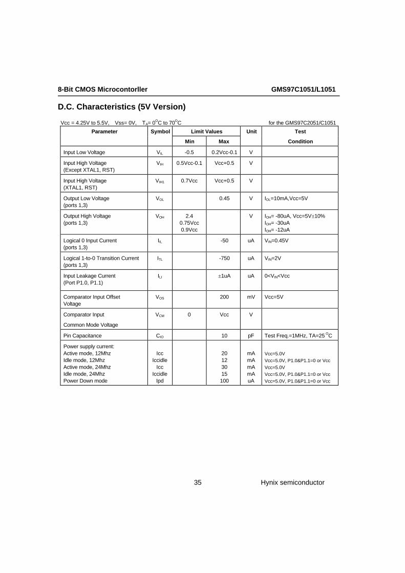
D.C. Characteristics (5V Version)
Vcc = 4.25V to 5.5V, Vss= 0V, TA= 0OC to 70OC for the GMS97C2051/C1051
Parameter Symbol Limit Values Unit Test
Min Max Condition
Input Low Voltage VIL -0.5 0.2Vcc-0.1 V
Input High Voltage (Except XTAL1, RST)
VIH 0.5Vcc-0.1 Vcc+0.5 V
Input High Voltage (XTAL1, RST)
VIH1 0.7Vcc Vcc+0.5 V
Output Low Voltage (ports 1,3)
VOL 0.45 V IOL=10mA,Vcc=5V
Output High Voltage (ports 1,3)
VOH 2.4 0.75Vcc 0.9Vcc
V IOH= -80uA, Vcc=5V±10% IOH= -30uA IOH= -12uA
Logical 0 Input Current (ports 1,3)
IIL -50 uA VIN=0.45V
Logical 1-to-0 Transition Current (ports 1,3)
ITL -750 uA VIN=2V
Input Leakage Current (Port P1.0, P1.1)
ILI ±1uA uA 0<VIN<Vcc
Comparator Input Offset Voltage
VOS 200 mV Vcc=5V
Comparator Input
Common Mode Voltage
VCM 0 Vcc V
Pin Capacitance CIO 10 pF Test Freq.=1MHz, TA=25 OC
Power supply current: Active mode, 12Mhz Idle mode, 12Mhz Active mode, 24Mhz Idle mode, 24Mhz Power Down mode
Icc
Iccidle Icc
Iccidle Ipd
20 12 30 15 100
mA mA mA mA uA
Vcc=5.0V
Vcc=5.0V, P1.0&P1.1=0 or Vcc
Vcc=5.0V
Vcc=5.0V, P1.0&P1.1=0 or Vcc
Vcc=5.0V, P1.0&P1.1=0 or Vcc

GMS97C1051/L1051 8-Bit CMOS Microcontroller
Hynix semiconductor 36
D.C. Characteristics (3V Version)
Vcc = 2.7V to 3.6V, Vss= 0V, TA= 0OC to 70OC for the GMS97L2051/L1051
Parameter Symbol Limit Values Unit Test
Min Max Condition
Input Low Voltage VIL -0.5 0.2Vcc-0.1 V
Input High Voltage (Except XTAL1, RST)
VIH 0.5Vcc-0.1 Vcc+0.5 V
Input High Voltage (XTAL1, RST)
VIH1 0.7Vcc Vcc+0.5 V
Output Low Voltage (ports 1,3)
VOL 0.45 V IOL=6mA,Vcc=2.7V
Output High Voltage (ports 1,3)
VOH 0.75Vcc 0.9Vcc
V IOH= -30uA IOH= -12uA
Logical 0 Input Current (ports 1,3)
IIL -50 uA VIN=0.45V
Logical 1-to-0 Transition Current (ports 1,3)
ITL -750 uA VIN=2V
Input Leakage Current (Port P1.0, P1.1)
ILI ±1uA uA 0<VIN<Vcc
Comparator Input Offset Voltage
VOS 200 mV Vcc=3V
Comparator Input
Common Mode Voltage
VCM 0 Vcc V
Pin Capacitance CIO 10 pF Test Freq.=1MHz, TA=25 OC
Power supply current: Active mode, 12Mhz Idle mode, 12Mhz Power Down mode
Icc
Iccidle Ipd
10 5 50
mA mA uA
Vcc=3V Vcc=3V, P1.0&P1.1=0 or Vcc Vcc=3V, P1.0&P1.1=0 or Vcc

8-Bit CMOS Microcontorller GMS97C1051/L1051
Hynix semiconductor 37
External Clock drive waveforms
tCHCX
tCLCL
tCLCX
tCHCX tCLCH
0.7 VCC
0.2 VCC - 0.1V
0.45V
VCC - 0.5 V
tCHCL
External Clock Drive
Symbol Parameter GMS97L2015/L1051 GMS97C2051/C1051
Min Max Min Max
Units
1/tCLCL Oscillator Frequency 0 12 0 24 MHz
tCLCL Clock Period 83.3 41.6 ns
tCHCX High Time 30 15 ns
tCLCX Low Time 30 15 ns
tCLCH Rise Time - 20 - 20 ns
tCHCL Fall Time - 20 - 20 ns
AC Testing Input/Output Waveforms(1)
VCC - 0.5V
0.45V
0.2VCC + 0.9V
TEST POINTS
0.2VCC - 0.1V
Note: 1. AC Inputs during testing are driven at VCC - 0.5V for a logic 1 and 0.45V for a logic 0. Timing measurements are made at VIH min. for a logic 1 and VIL max. for a logic 0.
Float Waveforms(1)
VLOAD + 0.1V
VLOAD
VLOAD - 0.1V
VOL + 0.1V
VOL + 0.1V
Timing Reference
Points
Note: 1. For timing purposes, a port pin is no longer floating when a 100mV change from load voltage occurs. A port pin begins to float when a 100mV change from the loaded VOH/VOL level occurs.
GMS97C1051/L1051 8-Bit CMOS Microcontroller
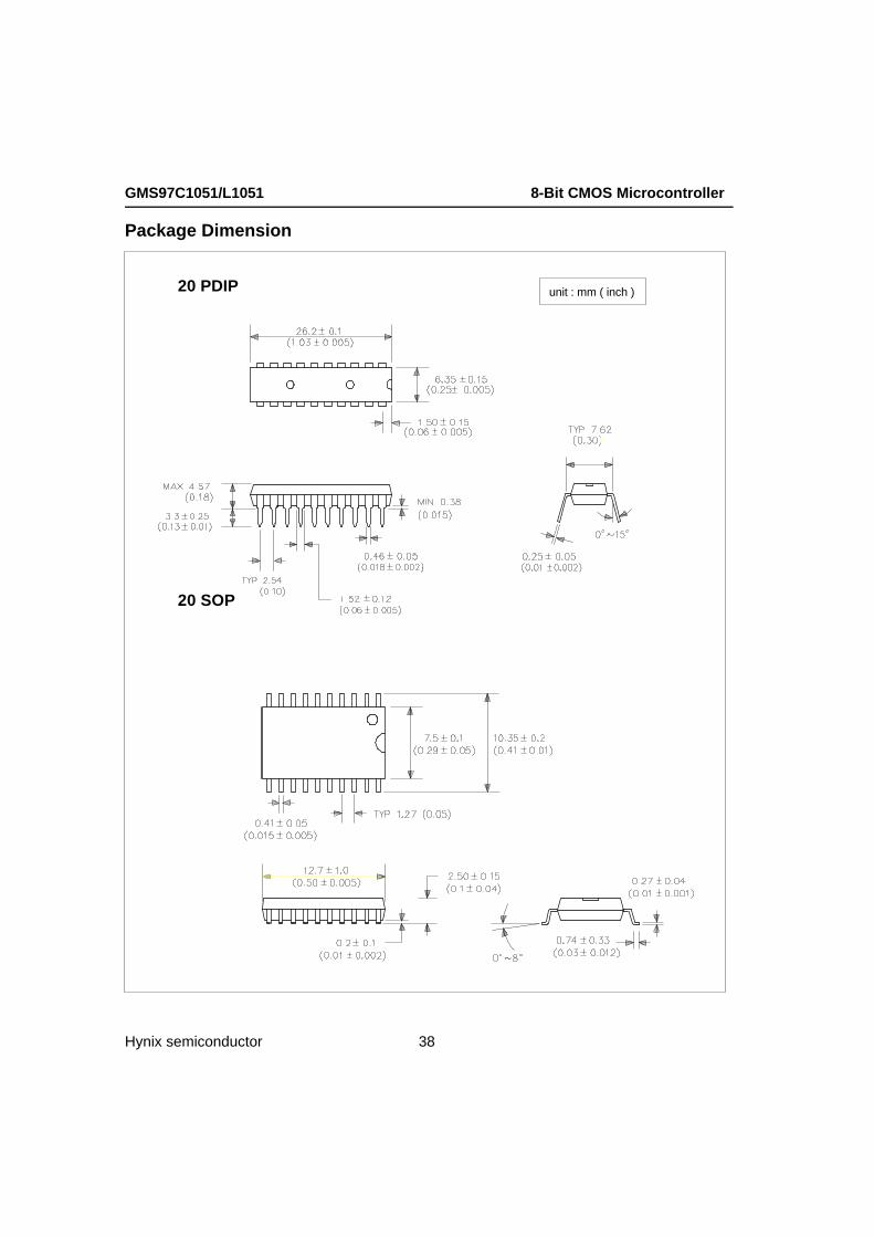
Hynix semiconductor 38
Package Dimension
20 PDIP
20 SOP
unit : mm ( inch )

8-Bit CMOS Microcontorller GMS97C1051/L1051
Hynix semiconductor 39
Ordering Information
Speed ( MHz) Power Supply Ordering Code Package Operation Range
12 2.7V to3.6V GMS97L1051 20 PDIP
GMS97L1051-D 20 SOP
4.25V to 5.5V GMS97C1051 20 PDIP Commercial
GMS97C1051-D 20 SOP (0¡ É to 70¡ É)
24 4.25V to 5.5V GMS97C1051-24 20 PDIP
GMS97C1051-24D 20 SOP
Package Type
20 PDIP 20 Lead, 0.300¡ ÈWide, Plastic Dual Inline Package (PDIP)
20 SOP 20 Lead, 0.300¡ ÈWide, Plastic Gull Wing Small Outline (SOP)


