
IBIS OPEN FORUMI/O BUFFER MODELING COOKBOOK
Version 4.0Revision 0.9
Prepared By:The IBIS Open Forum
Senior Editor:Michael MirmakIntel Corp.
Contributors:John Angulo, Mentor Graphics Corp.Ian Dodd, Mentor Graphics Corp.Lynne Green, Green Streak ProgramsSyed Huq, Cisco SystemsArpad Muranyi, Intel Corp.Bob Ross, Teraspeed Consulting Group
From an original by Stephen Peters
Rev 0.0 – August 10, 2004 Rev 0.1 – September 9, 2004 Rev 0.2 – October 5, 2004 Rev 0.3 – October 7, 2004 Rev. 0.4 – October 15, 2004 – added series/series switch descriptions; incorporated written
feedback from Arpad, updated the single-ended totem-pole buffer diagrams, reformatted document with appropriate labels and table of contents; used buffer or component in place of device in many cases; incorporated new SSO language; added new differential type diagrams.
Rev. 0.5 – October 21, 2004 – minor editorial changes, including fonts on examples; added captions to all drawings; added a new [Pin Mapping] description, with diagram; added diagrams to the “Series Element “ section
Rev. 0.6a – November 19, 2004 – added missing table and figure captions, inserted table of figures and table of captions, added A. Muranyi’s suggested changes from Nov. 18 Cookbook meeting; added note regarding pin-to-pad bijective mapping; revised differential section to describe systems before buffers; revised most curve figures; added detail on [Ramp] calculation and matching to I-V table data; grammar and spelling check completed
Rev. 0.6b – November 23, 2004 – updated clamp analysis and on-die termination text to account for differences between specification and A. Muranyi algorithms. Cookbook now recommends the Muranyi ranges for clamp generation and Muranyi methods of subtraction
Rev. 0.7 – December 22, 2004 – made changes suggested by A. Muranyi, including
o Additional line breaks before and after each sectiono Expanded [Pin Mapping] exampleo Updated differential comments
Rev. 0.8 – May 25, 2005 – incorporates three subdrafts from A. Muranyi Rev. 0.9 – June 13, 2005 – updated with cleanup changes by M. Mirmak
Incorporated changes from Bob Ross, including CAE-> EDA tool vendors,standardized indents of bullets, table changes, use of “tables” in place of “curves,” etc.
Also added two previously missing drawings
1.0 INTRODUCTION................................................................................................................................... 1
1.1 OVERVIEW OF AN IBIS FILE................................................................................................................... 11.2 STEPS TO CREATING AN IBIS MODEL......................................................................................................2
2.0 PRE-MODELING STEPS....................................................................................................................... 3
2.1 BASIC DECISIONS................................................................................................................................... 32.1.1 Model Version and Complexity......................................................................................................... 32.1.2 Specification Model vs. Part Model..................................................................................................32.1.3 Fast and Slow Corner Model Limits..................................................................................................42.1.4 Inclusion of SSO Effects.................................................................................................................... 4
2.2 INFORMATION CHECKLIST...................................................................................................................... 42.3 TIPS FOR COMPONENT BUFFER GROUPING..............................................................................................6
3.0 EXTRACTING THE DATA................................................................................................................... 6
3.1 EXTRACTING I-V DATA FROM SIMULATIONS...........................................................................................63.1.2 Sweep Ranges................................................................................................................................... 83.1.3 Making Pullup and Power Clamp Sweeps Vcc Relative.....................................................................93.1.4 Diode Models.................................................................................................................................... 9
3.2 EXTRACTING RAMP RATE OR V-T WAVEFORM DATA FROM SIMULATIONS..............................................93.2.1 Extracting Data for the [Ramp] Keyword..........................................................................................93.2.2 Extracting Data for the Rising and Falling Waveform Keywords.....................................................103.2.3 Minimum Time Step......................................................................................................................... 123.2.4 Multi-Stage Drivers......................................................................................................................... 123.2.5 Differential Buffers......................................................................................................................... 12
3.3 OBTAINING I-V AND SWITCHING INFORMATION VIA LAB MEASUREMENT..............................................36
4.0 PUTTING THE DATA INTO AN IBIS FILE......................................................................................37
4.1 BASIC SYNTAX: KEYWORDS AND THEIR DEFINITIONS...........................................................................374.1.1 IBIS File Header Information..........................................................................................................374.1.2 Component and Pin Information......................................................................................................384.1.3 The [Model] Keyword..................................................................................................................... 39
4.2 DATA CHECKING.................................................................................................................................. 524.2.1 Data Completeness.......................................................................................................................... 524.2.2 I-V and V-T Matching..................................................................................................................... 53
4.3 DATA LIMITING.................................................................................................................................... 554.4 ADDITIONAL RECOMMENDATIONS........................................................................................................57
4.4.1 Internal Terminations...................................................................................................................... 574.4.2 V-T Table Windowing...................................................................................................................... 61
4.5 ADVANCED KEYWORDS AND CONSTRUCTS...........................................................................................614.5.1 [Model Selector]............................................................................................................................. 624.5.2 [Submodel]..................................................................................................................................... 634.5.3 [Model Spec].................................................................................................................................. 644.5.4 [Driver Schedule]........................................................................................................................... 644.5.5 [Pin Mapping]................................................................................................................................ 654.5.6 Series Elements............................................................................................................................... 674.5.7 [Diff Pin]........................................................................................................................................ 72
5.0 VALIDATING THE MODEL...............................................................................................................72
6.0 CORRELATING THE DATA.............................................................................................................. 73
7.0 RESOURCES......................................................................................................................................... 74

Figure 3.1 - Standard 3-state Buffer........................................................................................................7
Figure 3.2 - Simulation Setup for Extracting Ramp Rate Information (Rising Edge Shown)..................10
Figure 3.3 – Device with Independent Input, Output and Power Supply Ports........................................13
Figure 3.4 – Device with Ports Using Common Ground........................................................................13
Figure 3.5 – Input Port with Locally Generated Reference.....................................................................14
Figure 3.6 – Single Ended Receiver......................................................................................................15
Figure 3.7 – True Differential Receiver.................................................................................................15
Figure 3.8 – Half Differential Receiver..................................................................................................16
Figure 3.9 – Pseudo Differential Receiver.............................................................................................17
Figure 3.10 – Single Ended Driver........................................................................................................17
Figure 3.11 – True Differential Driver with External Load....................................................................18
Figure 3.12 – Half Differential Driver with External Load.....................................................................19
Figure 3.13 – Pseudo Differential Driver Example................................................................................20
Figure 3.14 – Block Diagram of a True Differential Model using IBIS v3.2 Constructs.........................22
Figure 3.15 - I-V Table Extraction Fixture for a Differential Buffer.......................................................23
Figure 3.16 - Surface Plots of Raw Data from I-V Sweep of Differential Buffer....................................24
Figure 3.17 - I-V Curves of Common Mode Characteristics of Differential Buffer.................................25
Figure 3.18 – Differential Current Plot of Output Current versus P and N Voltage.................................25
Figure 3.19 - Plots of Various Vds Values for a [Series MOSFET] Buffer.............................................26
Figure 3.21 – Block Diagram of a Two-Tap Differential Buffer Featuring Pre-Emphasis.......................30
Figure 3.22 - Output of a Scheduled Driver Configured as an Inverter...................................................31
Figure 3.23 - Fixture for Extraction of C_comp Information..................................................................33
Figure 3.24 - Surface Plot of Buffer Capacitance versus Frequency and DC Bias Voltage......................34
Figure 3.25 - Fixture for Extraction of Differential Buffer C_comp.......................................................34
Figure 3.26 - Surface Plot of Differential Capacitance versus Frequency and DC Bias Voltage..............35
Figure 4.1 – Conceptual Diagram of Model Keyword Structure.............................................................41
Figure 4.2 – Model Keyword Structure with Added Diode Detail..........................................................42
Figure 4.3 – Graph of [GND Clamp] I-V Table Data.............................................................................44
Figure 4.4 – Graph of [POWER Clamp] I-V Table Data after Clamp Subtraction..................................45
Figure 4.5 – Raw I-V and Extrapolated Final [GND Clamp] Data Graphs..............................................45
Figure 4.6 – Raw I-V and Extrapolated Final [POWER Clamp] Data Graphs........................................46
Figure 4.7 – Graph of [Pulldown] I-V Table Data, after Clamp Subtraction...........................................47
Figure 4.8 – Graph of [Pullup] I-V Table Data after Clamp Subtraction.................................................48
Figure 4.9 – Diagram of Resistive Load for Rising Waveform...............................................................53
Figure 4.10 – V-T Table Loading Example...........................................................................................54
Figure 4.11 – V-T Table Loading Example, Simplified.........................................................................54
Figure 4.12 – [Pullup] I-V Table Data with Load Line Intercept............................................................55
Figure 4.13 – Data Point Selection Example..........................................................................................56
Figure 4.14 – Diagram of I/O Buffer with Internal Termination.............................................................57
Figure 4.15 – Raw I-V Table Clamp Data for Ground-connected Termination.......................................58
Figure 4.16 – Graph of I-V Data for Ground Terminated Buffer in High-Impedance State.....................59
Figure 4.17 – Graph of Power and Ground Clamp I-V Data for Vcc-connected Termination..................60
Figure 4.18 – Graph of I-V Data for Vcc Terminated Buffer in High-Impedance State...........................61
Figure 4.19 – Component Diagram Showing Buffer and Supply Buses..................................................66
Figure 4.20 – Connection of Single-ended and Series [Model]s.................................................68
Table 1 – Recommended Load Circuits and Waveforms for V-T Data Extraction..................................11
Table 2 – IBIS File Header Keywords...................................................................................................38
Table 3 – IBIS Component and Pin Information....................................................................................39
Table 4 – IBIS [Model] Subparameters.................................................................................................40
Table 5 – IBIS [Model] Temperature and Voltage Keywords.................................................................40
Table 6 – [Model] I-V Table Keywords.................................................................................................42
Table 7 – Pulldown I-V Table (Typical Only).......................................................................................47
Table 8 – [Ramp] and Waveform Table Keywords................................................................................49
Table 9 – I-V Table Keywords and Buffer Types...................................................................................51
Table 10 – V-T Fixtures and Buffer Types............................................................................................51
Table 11 – Example V-T Table Data for Rising Waveform....................................................................53
Table 12 – V-T Table Loading Recommendations.................................................................................55
1.0 Introduction
This cookbook describes the steps required to produce IBIS models for digital integrated circuits (ICs). IBIS (officially, EIA standard 656-A-1999, IEC 62014-1) stands for I/O Buffer Information Specification. IBIS models provide a standardized way of representing the electrical characteristics of an digital IC’s pins (input, output, or I/O buffers) behaviorally, i.e., without revealing the underlying circuit’s structure or process information.
The purpose of this document is to describe how to gather the information required to produce an IBIS model, as well as some of the common pitfalls to avoid when creating the IBIS file itself. Note that the basic behavioral information in an IBIS model can be obtained either by direct measurement of the component or transistor level simulation of the component’s buffers. This cookbook describes both methods. The cookbook is targeted towards generating models of CMOS, GTL, and bipolar parts, and applies to models generated for IBIS versions 3.2 and 4.0. For the most recent version of the specification and other IBIS documents visit the IBIS web page. For access information, see Resources later in this cookbook.
The intended audience of this cookbook is those responsible for performing the measurements or simulations that gather I/O buffer data, as well as those responsible for actual IBIS model creation. Persons involved in SI or system level PC board simulations may also benefit by reading this document. It is assumed that the reader has some familiarity with behavioral modeling of I/O buffers and analog simulation.
1.1 Overview of an IBIS File
An IBIS file contains, in a human readable ASCII format, the data required to behaviorally model a component’s input, output and I/O buffers. Specifically, the data in an IBIS file is used to construct a model useful for performing signal integrity (SI) simulations and timing analysis of printed circuit (PC) boards. The fundamental information needed to perform these simulations is a buffer’s I-V (current vs. voltage) and switching (output voltage vs. time) characteristics. Please note that the IBIS specification does NOT define an executable simulation model – it is a standard for the formatting and transfer of data. As such, the specification defines what the information included in an IBIS file represents and how it is to be gathered. It does not specify what an analog simulation application does with the data.
IBIS models are component-centric. That is, an IBIS file allows one to model an entire component, not just a particular input, output or I/O buffer. Therefore, in addition to the electrical characteristics of a component’s buffers an IBIS file includes a component’s pin-to-buffer mapping, and the electrical parameters of the component’s package.
In general an output or I/O buffer is characterized behaviorally using the following information: The buffer’s output I-V characteristics when the output is in the logic low state The buffer’s output I-V characteristics when the output is in the logic high state The buffer’s output I-V characteristics when the output is forced below ground and above the power
supply rail (referred to as its ‘beyond the rail’ characteristics) The time it takes a buffer’s output to switch logic states (i.e. from low to high and high to low) The buffer’s capacitance
For an input buffer the required information is reduced to: The buffer’s I-V characteristics (including its ‘beyond the rail’ characteristics) The buffer’s capacitance
IBIS Forum I/O Buffer Modeling Cookbook Page 1
The above information is included in an IBIS file using ‘keywords’. A keyword is a word or phrase surrounded by square brackets. Keywords are followed either by specific parameters or tables of data. For instance, the [Model] keyword would be used to encapsulate the I-V and V-T tables, plus other data, for individual single-ended I/O buffer. Some keywords are required, but most are optional. At a minimum, a valid IBIS file contains the following data and keywords:
1. Information regarding the file itself and name of the component being modeled. This information is contained under the keywords [IBIS Ver], [File Name], [File Rev], [Component] and [Manufacturer].
2. Information about the package’s electrical characteristics and the pin to buffer model mapping (i.e. which pins are connected to which buffer models). This information is included under the [Package] and [Pin] keywords.
3. The data required to model each unique input, output and I/O buffer design on the component. The [Model] keyword introduces the data set for each unique buffer. As described above, buffers are characterized by their I-V behaviors and switching characteristics. This information is included using the keywords [Pullup], [Pulldown], [GND clamp], [POWER Clamp] and [Ramp]. In addition, the required parameters to the [Model] keyword specify a model’s type (Input, Output, I/O, Open_drain, etc.) and its input or output capacitance.
The details of constructing an IBIS model from data are included in the Putting the Data Into an IBIS File chapter later in this document.
1.2 Steps to creating an IBIS Model
There are five basic steps to creating an IBIS model of a component:1. Perform the pre-modeling activities. These include deciding on the model’s complexity, determining
the voltage, temperature and process limits over which the IC operates and the buffer model will be characterized, and obtaining the component related (electrical characteristics and pin-out) and use information about the component. See the chapter titled Pre-Modeling Steps.
2. Obtain the electrical (I-V tables and rise/fall) data for output or I/O buffers either by direct measurement or by simulation. See the chapter titled Extracting the Data. This chapter may also be used by those who are doing the simulations required to gather the data but not actually creating the IBIS file.
3. Format the data into an IBIS file and run the file through the Golden Parser. See the chapter titled Putting the Data Into an IBIS File.
4. If the model is generated from simulation data, validate the model by comparing the results from the original analog (transistor level) model against the results of a behavioral simulator that uses the IBIS file as input data. See the chapter titled Validating the Model.
5. When the actual silicon is available (or if the model is from measured data), compare the IBIS model data to the measured data. See the chapter titled Correlating the Data.
The rest of this cookbook documents these steps in detail.
Page 2 I/O Buffer Modeling Cookbook IBIS Open Forum
2.0 Pre-Modeling Steps
2.1 Basic Decisions
Before one creates an I/O buffer model there are several basic questions that must be answered regarding the model’s complexity, operational limits, and use requirements. Answering these questions requires not only a knowledge of the buffer’s physical construction, but also a knowledge of the final application in which the IC will be used, and any specific requirement the model users may place on the model. These questions cannot be answered by the model creator alone; they generally require the involvement of both the buffer designer and members of the team responsible for insuring that the I/O buffers are useable in a system environment. This team is referred to as the interconnect simulation team. Together, the model creator and interconnect simulation team must determine the following:
2.1.1 Model Version and Complexity
Based on the characteristics and construction of the I/O buffer itself, and the model user’s simulator capability, you must decide what IBIS version of the model is most appropriate. Different IBIS versions, as denoted by the [IBIS Ver] keyword, support different features. Additionally, the checking rules used by the IBIS Golden Parser change slightly with each version. In general, models should use the highest [IBIS Ver] version number supported by the Golden Parser and by their simulation tools. Similarly, following good engineering practice, use the simplest model that will suffice.
For standard CMOS buffers with a single stage push-pull or open drain outputs, a version 1.1 model is the starting point. A version 1.1 model describes a buffer using a low state and high state I-V table, along with a linear ramp that describes how fast the buffer switches between states. IBIS version 2.1 adds support for tables of V-T data, in addition to support for ECL and dual-supply buffers, ground bounce from shared power rails, differential I/O buffers, termination components, and controlled rise-time buffers. A version 2.1 or above model will be required if the I/O buffer has any of the following characteristics:
Multiple Supply Rails -- A version 2.1 (or higher) model is required if the buffer contains diode effects – from parasitic diodes or Electrostatic Discharge (ESD) diodes – which are referenced to a different power rail than the pullup or pulldown transistors, or if the I/O uses more than one supply (for example, a buffer whose output swings from below ground or above Vcc).
Non-Linear Output Switching Waveform – A version 2.1 (or higher) model is required if the I/O buffer’s output voltage vs. time waveform (its V-T waveform) when switching low-to-high or high-to-low cannot be accurately described using a linear ramp rate value. This is the case for GTL technology, or for any buffer that uses “graduated turn on” type technology.
In addition, a version 2.1 model description is required if the model maker wishes to enable the user to perform ground bounce simulations by connecting several buffers together on a common supply rail. See the [Pin Mapping] keyword description below.
IBIS version 3.2 and above support an electrical board description, multi-staged buffers or buffers which may use multiple I-V tables and diode transient times, among other features.
2.1.2 Specification Model vs. Part Model
IBIS Forum I/O Buffer Modeling Cookbook Page 3
A model can be made to represent a particular existing component or can be made as a representative encapsulation of the limits of the specification for a class of components. Specification vs. Part is a major factor in determining if and how much guard-banding or de-rating a model requires. Generally, a “spec model” is based on an existing part, then the strength and edge rate of the model is adjusted to meet the best and worst case parameters of a particular specification. For example, an GTL buffer model for a particular processor may give a worst case Vol of 0.4 V at 36 mA. However, if the GTL specification allows for a worst case Vol of 0.6 V at 36 mA the model’s pulldown table may be adjusted (or de-rated) to describe the specification and not just the behavior of an individual part.
2.1.3 Fast and Slow Corner Model Limits
The IBIS format provides for slow (weakest drive, slowest edge), typical and fast (strongest drive, fastest edge) corner models. These corners are generally determined by the environmental (temperature and power supply) conditions under which the silicon is expected to operate, the silicon process limits, and the number of simultaneous switching outputs. The interconnect team or project must supply the model developer with the environmental, silicon process, and operational (number of SSOs) conditions that define the slow, typical and fast corners of the model. Please note that for an output buffer model to be useful for flight time simulations these conditions MUST match those used for specifying the buffer’s Tco parameter.
2.1.4 Inclusion of SSO Effects
Closely related to the discussion on model limits is the decision on how to include Simultaneous Switching Output (SSO) effects. SSO effects can be included explicitly in a model by measuring the I-V and edge rate characteristics under SSO conditions. For example, a buffer’s I-V characteristic can be measured with all the adjacent buffers turned on and sinking current, or the buffer’s edge rate may be measured while adjacent buffers are also switching. Alternatively, a model that represents a single buffer in isolation may be created, then several buffers may be connected to a common power or ground rail via the [Pin Mapping] keyword. The former method (including SSO effects in the I-V and V-T tables) has the advantage that the resulting model is straight forward to verify and less dependent on any particular simulator’s capability. Note however, the [Pin Mapping] keyword method does give the user the ability to perform explicit ground bounce simulations and devise specific ‘what if’ scenarios.
Note that the information provided under IBIS 4.0 and earlier versions only describes the output behavior of buffers under loaded conditions. Therefore, SSO simulations will only be based on the behavior at the pad and not upon information extracted about the current profile of the supplies as the buffer switches. Different distributions of internal buffer current may result in the same behavior at the pad. Different simulation tools may therefore make radically different assumptions regarding SSO behavior for the same IBIS data. Check with your simulation tool vendor for details on their specific assumptions and IBIS SSO simulation algorithms.
2.2 Information Checklist
Once the above decisions have been made, the model maker can begin the process of acquiring the specific information needed to generate the IBIS model for the component. Some of this information is specific to the component as a whole and goes directly into the IBIS file itself, while some items are needed to perform the required simulations. In general, the model maker will need the following:
IBIS Specification Acquire, read and become familiar with the IBIS specification.
Page 4 I/O Buffer Modeling Cookbook IBIS Open Forum
Buffer Schematics Acquire a schematic of each of the different types of input, output and I/O buffers on the component. If at all possible, use the same schematic that the silicon designers use for simulating Tco. Make sure that the schematic includes ESD diodes (if present in the design) and a representation of the power distribution network of the package. From these schematics determine the type of output structure (standard CMOS totem-pole, open-drain, etc.) for each different type of output or I/O buffer on the IC.
Clamp Diode and Pullup References Determine if the buffer uses a different voltage reference (power supply rail) for the clamp diodes than that used for the pullup or pulldown transistors. This may be the case when dealing with components that are designed to be used in mixed 3.3 V/5 V systems.
Packaging Information Find out in what packages the component is offered. A separate IBIS model is required for each package type. Acquire a pinout list of the component (pin name to signal name mapping) and determine the pin name to buffer type mapping.
Packaging Electricals Acquire the electrical characteristics (inductance, capacitance and resistance) of the component’s package for each pin to buffer connection (package stub). This becomes the R_pin, L_pin and C_pin parameters of the [Pin] keyword or the R_pkg, L_pkg and C_pkg of the [Package] keyword.
Signal Information Determine which signals can be ignored for modeling purposes. For example, test pads or static control signals may not need a model. These may be listed as NC in the [Pin] list.
Die Capacitance Obtain the capacitance of each pad (the C_comp parameter). This is the capacitance seen when looking from the pad back into the buffer for a fully placed and routed buffer design, exclusive of package effects (note that the phrases “Cdie” or “die capacitance” may be used in other industry contexts to refer to the capacitance of the entire component, in some cases including package capacitance, as measured between the power and ground supply rails).
Vinl and Vinh Parameters A complete IBIS model of an input or I/O buffer includes the Vinl and Vinh parameters. Vinl is the maximum pad or pin voltage at which the receiving buffer’s logical state would still be a logical “low” or “0.” Vinh is the minimum pad or pin voltage at which the receiving buffer’s logical state would still be a logical “high” or “1.”
Tco Measurement Conditions Find out under what loading conditions an output or I/O buffer’s Tco (propagation delay, clock to output) parameter is measured. This includes the load capacitance, resistance and voltage (Cref, Rref and Vref parameters) as well as the output voltage crossing point at which Tco is measured (the Vmeas parameter).
IBIS Forum I/O Buffer Modeling Cookbook Page 5

2.3 Tips For Component Buffer Grouping
One of the first tasks when building an IBIS model of a component is determining how many individual buffer models have to be created. Separate buffer models are required for each different buffer design or structure (number and connection of the transistor elements) the component uses. Begin by first separating a component’s pins into inputs, outputs and I/Os. Then for each group of pins determine how many buffer designs are present. For example, a clock input may have a different input design or diode structure than the rest of the component’s inputs. Also, be aware that even if all the output or I/O signals are driven by the same buffer design, separate output or I/O models may be required if a group of signals have different C_comp parameters or Tco measurement conditions. Once the number of separate buffer models has been determined, the actual buffer model creation process can begin.
3.0 Extracting the Data
Once the pre-modeling steps have been performed, the process of gathering the required I-V and switching information can begin. Output and I/O buffers need both I-V tables and rise/fall data, while input buffer require I-V tables only. There are two ways to get this information:
For pre-silicon models use circuit simulation tools to obtain the information over the worst cases of process and temperature variations, then correlate the model against the actual silicon.
When the actual silicon is available, use the data from physical measurements to build the model. However, it is difficult to get worst case min and max data over process and temperature this way.
The first sections of this chapter explains how to obtain the I-V and V-T information from a transistor-level model of the buffer, either by use of an automated simulation template or extraction tool (such as S2IBIS3) or by doing your own simulations. Obtaining I-V and Switching Information via Lab Measurement later in this chapter explains how to gather this information via measurement. It is assumed that the reader has some background in doing transistor level simulations and/or the use of lab equipment.
3.1 Extracting I-V Data from Simulations
The first step to extracting the required I-V tables is understanding the buffer’s operation. Analyze the buffer schematic and determine how to put the buffer’s output into a logic low, logic high and (if applicable) high impedance (3-state) state. As mentioned above, the schematic should include the R, L and C parameters associated with the on-die power supply distribution and ground return paths as well as any ESD or protection diodes. The schematic should also indicate if the power clamp or ground clamp diode structures are tied to a voltage rail (voltage reference) different than that used by the pullup or pulldown transistors.
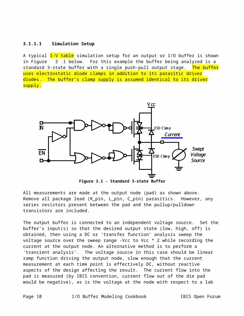
3.1.1.1 Simulation Setup
A typical I-V table simulation setup for an output or I/O buffer is shown in Figure 3.1 below. For this example the buffer being analyzed is a standard 3-state buffer with a single push-pull output stage. The buffer uses electrostatic diode clamps in addition to its parasitic driver diodes. The buffer’s clamp supply is assumed identical to its driver supply.
Page 6 I/O Buffer Modeling Cookbook IBIS Open Forum

Current
SweptVoltageSource
IN
EN
Vcc
ESD Clamp
ESD Clamp
Current
SweptVoltageSource
IN
ENEN
Vcc
ESD Clamp
ESD Clamp
Figure 3.1 - Standard 3-state Buffer
All measurements are made at the output node (pad) as shown above. Remove all package lead (R_pin, L_pin, C_pin) parasitics. However, any series resistors present between the pad and the pullup/pulldown transistors are included.
The output buffer is connected to an independent voltage source. Set the buffer’s input(s) so that the desired output state (low, high, off) is obtained, then using a DC or ‘transfer function’ analysis sweep the voltage source over the sweep range -Vcc to Vcc * 2 while recording the current at the output node. An alternative method is to perform a ‘transient analysis’. The voltage source in this case should be linear ramp function driving the output node, slow enough that the current measurement at each time point is effectively DC, without reactive aspects of the design affecting the result. The current flow into the pad is measured (by IBIS convention, current flow out of the die pad would be negative), as is the voltage at the node with respect to a lab reference, then the resulting I-T and V-T data is combined into a single I-V table. Note that a transient function analysis may require post simulation data manipulation.
3.1.1.2 3-state Buffers
For an I/O (3-stateable) buffer, four sets of I-V tables are only require generally included; one with the pulldown transistor turned on (output in the low state), one with the pullup transistor turned on (output in the high state), and two with the output in a high impedance state though. The data gathered while the output is in the low state is used to construct the [Pulldown] table. Data gathered when the output is in the high state is used to construct the [Pullup] table. Pulldown I-V data is referenced to ground while pullup I-V data is referenced to Vcc. (Referencing pullup data to Vcc means that the endpoints of the sweep range are adjusted as Vcc is adjusted; refer to the Making Pullup and Power Clamp Sweeps Vcc Relative section for more details) Data for the [GND Clamp] keyword is taken with the output in the high impedance state and is ground relative, while data for the [POWER Clamp] keyword is also taken with the output in a high impedance state but with the data Vcc relative. For each keyword, a typical set of tables must be included; data for repeated under the minimum, typical and maximum corner conditions may be included. If corner data is present, it and must cover the entire sweep range.
Thus, a buffer with 3-state capabilities would require the following 12 I-V data sets: Pulldown I-V under minimum, typical and maximum conditions, data ground relative Pullup I-V under minimum, typical and maximum conditions, data Vcc relative
IBIS Forum I/O Buffer Modeling Cookbook Page 7
High Impedance state I-V under minimum, typical and maximum conditions, data ground relative High Impedance state I-V under minimum, typical and maximum conditions, data Vcc relative
3.1.1.3 Output Only Buffers
For an output only (non 3-state) output buffer only two sets of tables are needed; one with the pulldown transistor turned on (output in the low state), and one with the pullup transistor turned on (output in the high state). As before, pulldown I-V data is referenced to ground while pullup I-V data is referenced to Vcc. Because an output only buffer does not have a 3-state mode the power and ground clamp diode tables cannot be isolated from the transistor tables; the beyond the rail data is simply included in the pullup and pulldown I-V data. The [GND Clamp] and [POWER Clamp] keywords are not required for an output only buffer.
3.1.1.4 Open Drain Buffers
Open-drain or open-collector type buffers only require generally contain three sets of I-V data: [Pulldown], [GND Clamp] and [POWER Clamp] (technically, clamp data is never required by the IBIS specification). Data for the [Pulldown] table is gathered as described previously. [POWER Clamp] and [GND Clamp] data is gathered by turning off the pulldown transistor then doing the two I-V sweeps as described above for an I/O buffer in the high impedance state. Note that an open drain buffer may not require the full -Vcc to Vcc * 2 sweep range; refer to the section below entitled Sweep Ranges.
3.1.1.5 Input Buffers
When gathering I-V data for input buffers the same general setup is used, only the variable voltage source is placed on the input node. Input buffers only require generally contain only [POWER Clamp] and [GND Clamp] I-V data, though [POWER Clamp] only or [GND Clamp] only buffers have been seen (technically, clamp data is never required by the IBIS specification). As with the output buffer, [GND Clamp] data is gathered via a voltage sweep with the voltage source referenced to ground and the [POWER Clamp] data is gathered by a voltage sweep with the voltage source Vcc relative. If an input buffer includes internal resistive terminations to power and/or ground, the effects of these terminations on the I-V tables are included into the respective ground clamp or power clamp I-V data and additional post-processing is required before the data can be included in the IBIS model. See Internal Terminations for more information.
3.1.2 Sweep Ranges
As per the IBIS specification I-V data must be supplied over the range of voltages the output could possible see in a transmission line environment. Assuming that a buffer’s output swings from ground to Vcc (where Vcc is the voltage given by the [Voltage Range] or [Pullup Reference] keywords) this range is -Vcc (the maximum negative reflection from a shorted transmission line) to Vcc *2 (the maximum positive reflection from an open circuited transmission line). However, be aware that if a buffer is operating in an environment where its output could be actively driven beyond these limits the I-V table must be extended further. Consider, for example, a 3.3 V I/O buffer operating in a mixed 3.3 V/5 V system. While the buffer’s output may only drive from 0 to 3.3 V, a five volt buffer connected to this output may drive the output node beyond 3.3 V volts. In this case I-V data should be supplied over a full -5 V to +10 V range. Likewise, an open collector or open drain buffer may be terminated in a voltage (Vpulllup) different than that given by the [Voltage Range] keyword. In this case it is recommended to supply the pullup and pulldown data over the range -Vpullup to Vpullup *2.
Page 8 I/O Buffer Modeling Cookbook IBIS Open Forum
It is recognized that semiconductor buffer models may not be well behaved over these ranges, so it is acceptable to lessen the actual sweep range then use linear extrapolation to get to the required endpoints. For example, suppose one were attempting to gather the I-V data for a typical 5 V buffer. The IBIS specification requires I-V data over the full -5 V to 10 V range. The model maker may choose to limit the simulation sweep to -2 V to +7 V, and then extrapolate to the final -5 V to +10 V range. Be aware however, that the simulation sweep range must be enough to forward bias any ESD/protection diodes or the diodes intrinsic to the output transistor structures.
3.1.3 Making Pullup and Power Clamp Sweeps Vcc Relative
As stated earlier the pullup and power clamp data is relative to Vcc. In order to make the pullup and power clamp data Vcc relative (and to enter this I-V data into IBIS’s table format properly) adjust the starting and ending endpoints of these sweep to follow the variations in Vcc. For example, suppose one where gathering the pullup data for a standard 3.3 V buffer whose Vcc specification was 3.3 V +/- 10% (i.e. the operating Vcc ranged from 3.0 V minimum to 3.6 V maximum). The sweep voltage under typical conditions would range from -3.3 V to +6.6 V. For minimum conditions, where the Vcc was adjusted to 3.0 V, the sweep voltage should also be adjusted negative 0.3 V, to sweep from -3.6 V to +6.3 V. Likewise, for maximum conditions, adjust the sweep endpoint positive 0.3 V so the sweep covers -3.0 V to 6.9 V. By gathering the data in this manner the corresponding voltage data point in all three data sets represent the same ‘distance’ from Vcc. Note that the 9.9 V sweep RANGE remains the same for all three simulations.
3.1.4 Diode Models
When doing digital I/O buffer designs most of the analysis is concerned with the buffer’s Tco parameter and output impedance. Very little attention is paid to a buffer’s ‘beyond the rail’ operation. Thus, the diode models included in buffer’s schematic may be included for layout or completeness only, and are most likely ‘perfect’ diodes with no intrinsic resistance. Likewise, if the design relies on the intrinsic diode structure of the output transistors to provide output protection the transistor models may not properly model this mode of operation. Therefore, when doing simulation in these voltage regions one may get unrealistically large (e.g., kiloamp) power and ground clamp currents. If this is a problem the model creator has a couple of options. Working with the buffer designer the diode or transistor models can be enhanced to include the proper junction or bulk resistance. Note that with large ESD structures the metal resistance can be relatively large—on the order of a few ohms – an this should be included in the design. If an actual buffer is available the model creator can measure the power and ground clamp I-V data directly.
3.2 Extracting Ramp Rate or V-T Waveform Data from Simulations
Simulations to obtain the ramp rate and/or V-T (output voltage vs. time) tables are relatively straight forward. For each simulation corner (minimum, typical, maximum) four V-T data sets are required; one rising and one falling set for the buffer output switching low to high and one rising and one falling set for the buffer output switching high to low. This data can then be reported as a rising and falling dV/dt ratios (the ‘ramp rate’) or the actual V-T data may be reported directly.
3.2.1 Extracting Data for the [Ramp] Keyword
IBIS Forum I/O Buffer Modeling Cookbook Page 9

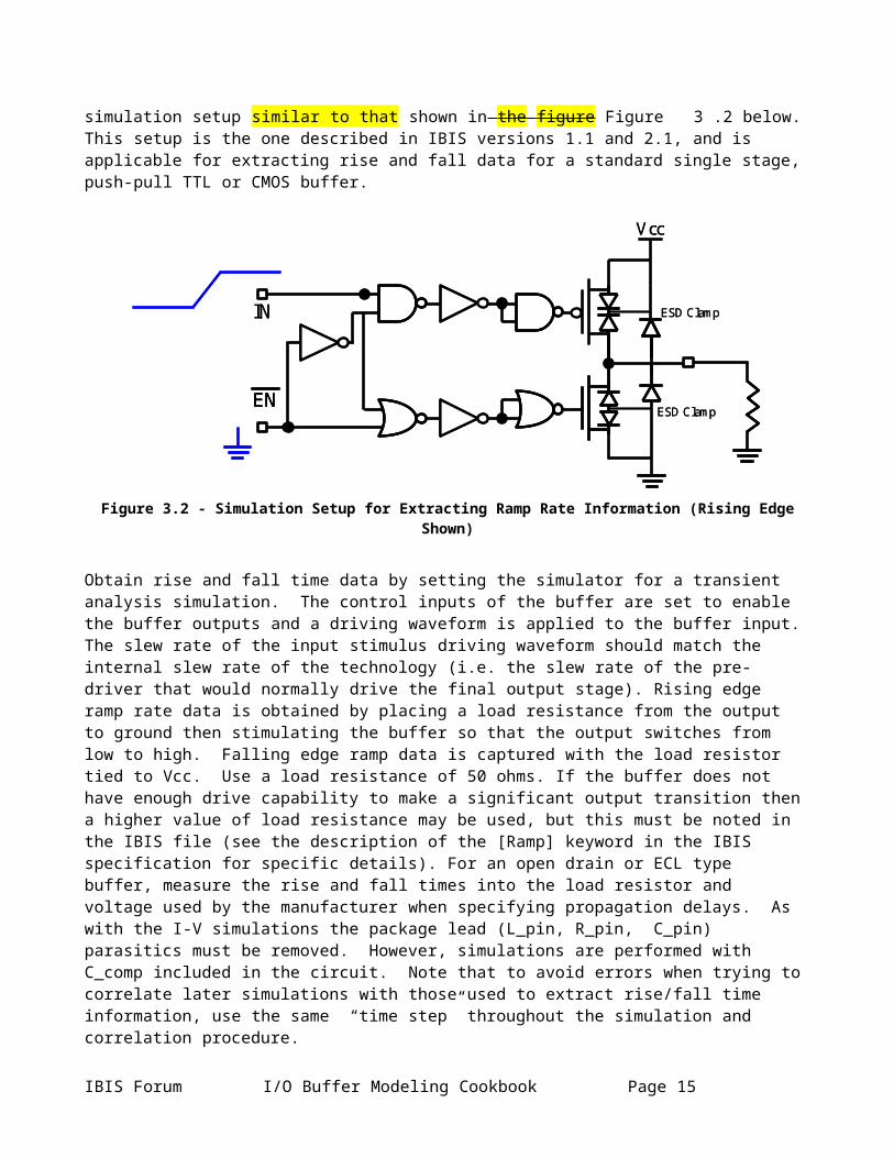
If the output switching (V-T) waveform of a buffer can be approximated by a linear ramp (i.e. the V-T waveform has no abrupt changes in shape, there are no ‘pedestals’ in the waveform, etc.) then the V-T data may be reported as a rising and falling ramp rate (dV/dt) by using the [Ramp] keyword. Data for the [Ramp] keyword may be extracted using the simulation setup similar to that shown in the figure Figure 3.2 below. This setup is the one described in IBIS versions 1.1 and 2.1, and is applicable for extracting rise and fall data for a standard single stage, push-pull TTL or CMOS buffer.
IN
EN
Vcc
ESD Clamp
ESD Clamp
IN
ENEN
Vcc
ESD Clamp
ESD Clamp
Figure 3.2 - Simulation Setup for Extracting Ramp Rate Information (Rising Edge Shown)
Obtain rise and fall time data by setting the simulator for a transient analysis simulation. The control inputs of the buffer are set to enable the buffer outputs and a driving waveform is applied to the buffer input. The slew rate of the input stimulus driving waveform should match the internal slew rate of the technology (i.e. the slew rate of the pre-driver that would normally drive the final output stage). Rising edge ramp rate data is obtained by placing a load resistance from the output to ground then stimulating the buffer so that the output switches from low to high. Falling edge ramp data is captured with the load resistor tied to Vcc. Use a load resistance of 50 ohms. If the buffer does not have enough drive capability to make a significant output transition then a higher value of load resistance may be used, but this must be noted in the IBIS file (see the description of the [Ramp] keyword in the IBIS specification for specific details). For an open drain or ECL type buffer, measure the rise and fall times into the load resistor and voltage used by the manufacturer when specifying propagation delays. As with the I-V simulations the package lead (L_pin, R_pin, C_pin) parasitics must be removed. However, simulations are performed with C_comp included in the circuit. Note that to avoid errors when trying to correlate later simulations with those used to extract rise/fall time information, use the same “time step” throughout the simulation and correlation procedure.
3.2.2 Extracting Data for the Rising and Falling Waveform Keywords
In IBIS versions 2.1 and above V-T data may be reported directly by using the [Rising Waveform] and [Falling Waveform] keywords. These two keywords are generally required if the output switching waveform of the buffer is significantly non-linear (this is the case with most ‘controlled rise time’ or ‘graduated turn on’ style buffers). The use of these keywords is also indicated if the buffer incorporates a delay between the turning off of one output transistor and the turning on of the other (i.e. the V-T waveform contains a pedestal). Finally, the model creator may wish to include the V-T data directly so that the model itself includes it own verification feature. By including this ‘golden waveform’ the model user may perform a simulation with the buffer driving
Page 10 I/O Buffer Modeling Cookbook IBIS Open Forum
the same load as was used to generate the V-T tables. The results of this simulation should match the V-T waveform as given in the IBIS file, thereby verifying that the users simulator is producing the proper results.
When performing simulations to extract V-T data for the [Rising Waveform] and [Falling Waveform] keywords a variety of load circuits may be used, depending on the technology of the buffer. The intent is that by picking the proper load(s) and termination voltage(s), the turn-on time, turn-off time (and overlap between the two) of the pullup and pulldown stages of the buffer can be isolated and a more accurate behavioral model constructed. Following are the recommended loads and waveforms to collect, as specified by the various EDA tool vendors that support IBIS models.
Technology # of Waveforms
Notes Load Circuit and Waveform
Standard Push/Pull – CMOS 4 (1) 1R + 1F driving 50 ohms to Vcc1R + 1F driving 50 ohms to GND
Standard Push/Pull – TTL 8 (1) 1R + 1F driving 50 ohms to 3.5v1R + 1F driving 50 ohms to GND1R + 1F driving 7 ohms to Vcc1R + 1F driving 500 ohms to GND
Open Drain/Collector– CMOS, TTL and GTL
2 (1) (2) 1R + 1F into manufactures suggested Vterm and Rterm (pullup resistor and voltage)
Open Source/Emitter – CMOS and TTL
2 (1) (2) 1R + 1F into manufactures suggested Vterm and Rterm (pulldown resistor and voltage)
ECL 2 (1) (2) 1R + 1F into manufactures suggested Vterm and Rterm (pulldown resistor and voltage)
Table 1 – Recommended Load Circuits and Waveforms for V-T Data ExtractionNote:(1) 1R = one rising waveform, 1F = one falling waveform(2) if recommended termination resistor is >100 ohms, include 1R +1F driving 50 ohms to Vterm
Note:Be aware that not all EDA tool vendors’ simulation software will use all the V-T tables provided in the model. If in doubt, check with your EDA tool vendor.
As with the simulations for ramp rate the slew rate of the driving waveform should match the internal slew rate of the technology. For meaningful results all of the above rising and falling waveforms should be taken with the package lead parameters (R_pin, L_pin and C_pin or R_pkg, L_pkg and C_pkg) and fixture reactive elements (L_fixture and C_fixture) set to zero. (The L_fixture and C_fixture parameters are included as parameters of the [Rising Waveform] and [Falling Waveform] keywords only for use in documenting a measurement setup or creating complex loads for simulator comparison and validation via a golden waveform.) As noted in the IBIS specification itself, it is critical that all rising and falling waveforms be time correlated. In other words, the rising (falling) edge data in each of the rising (falling) edge waveform tables must be entered with respect to a common reference point on the input waveform used to stimulate the buffer.
In addition to the above recommended V-T tables, additional waveforms may be included for simulator validation purposes. These waveforms are referred to as ‘golden waveforms’ because their intent is to supply a reference waveform that the simulator attempts to match, not raw V-T data that the simulator uses to construct the behavioral model. Unlike the recommend loads above, the load circuits used to generate golden waveforms
IBIS Forum I/O Buffer Modeling Cookbook Page 11
can include reactive elements. Two popular golden waveform loads are 50 ohms to (Vcc - GND) / 2, and a 50 pF load to ground. The model maker may also wish to include a waveform of the buffer driving a load that represents the typical load found in the buffer’s intended application.
Finally, some buffers may show slightly different rising and falling edge characteristics depending on how much time the buffer has had to settle from a previous output transition. Some projects may ask that the model creator extract ramp or V-T data from the second or third output transition in a series.
3.2.3 Minimum Time Step
As a rule of thumb, set the minimum time step so that there are between 30 to 50 data points in a rising or falling V-T table. If the V-T waveform is especially complex more points may be required (note however that the V-T waveform tables can contain no more than 100 points under IBIS 3.2; IBIS 4.0 permits up to 1000 points per V-T waveform). If the data is going to be reduced to dV/dt under the [Ramp] keyword then fewer points may be required.
3.2.4 Multi-Stage Drivers
Some buffer designs involve staged or graduated activation of the buffer as a function of time. For these buffers, a single set of V-T and I-V tables may only correctly describe one of the stages through which the buffer passes in any one transition. In this case, the [Driver Schedule] keyword may be used to combine several sets of V-T and I-V tables as a function of time. See [Driver Schedule] below.
Collecting data on multi-stage drivers is highly dependent on the structure of the buffer. If
{pre-emphasis?}
SECTION INCOMPLETE
3.2.5 Differential Buffers
{to be added}
3.2.5.1 Introduction
Today’s high-speed designs make increasing use of various kinds of differential buffers and signaling techniques. Unfortunately the related terminology is not always defined unambiguously. Therefore this chapter will begin with a short overview of the fundamental concepts of differential and single ended signaling, and the basic operation of differential drivers and receivers. In order to understand the IBIS model making process of differential buffers it is very important to understand these basic principles.
The main difference between differential and single ended signaling is very closely related to how voltages and/or currents are observed by the receiver and/or generated by the driver. We should all remember from basic electronics or physics courses that a voltage can only be measured between two points. (There is no such thing as a voltage of a single point). Similarly, current makes only sense when we talk about a path (or branch), through which current can flow. Since a current path is basically an electrical connection between two points, a relationship between voltage and current can be easily established. From this perspective, all voltage and
Page 12 I/O Buffer Modeling Cookbook IBIS Open Forum
current measurements or observations are differential in nature, because they involve two disctinct points in space. These principles are valid regardless of whether the voltages and currents we are observing represent signals or power.
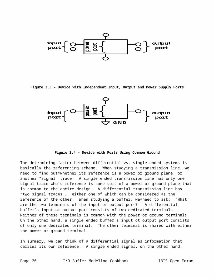
Most electronic circuits are designed to amplify and/or process signals. To do this, they consume power. The simplest circuit, having an input, output and power supply port, will need a total of six terminals if each of these ports are to be kept independent (or isolated) from each other. However, the usage of a common reference can reduce the total number of terminals to just four. In practical designs, such simplifications can provide significant cost savings and reduction of complexity, especially on large designs. Whether or not such simplifications can be done depends on many different requirements, such as safety, cost, and performance, just to name a few.
Figure 3.3 – Device with Independent Input, Output and Power Supply Ports
Figure 3.4 – Device with Ports Using Common Ground
The determining factor between differential vs. single ended systems is basically the referencing scheme. When studying a transmission line, we need to find out whether its reference is a power or ground plane, or another “signal” trace. A single ended transmission line has only one signal trace who’s reference is some sort of a power or ground plane that is common to the entire design. A differential transmission line has “two signal traces”, either one of which can be considered as the reference of the other. When studying a buffer, we need to ask: “What are the two terminals of the input or output port?” A differential buffer’s input or output port consists of two dedicated terminals. Neither of these terminals is common with the power or ground terminals. On the other hand, a single ended buffer’s input ot output port consists of only one dedicated terminal. The other terminal is shared with either the power or ground terminal.
IBIS Forum I/O Buffer Modeling Cookbook Page 13
In summary, we can think of a differential signal as information that carries its own reference. A single ended signal, on the other hand, does not include a reference because it is assumed to be available either as a common power or ground connection, or as a locally generated reference which is derived from a common power or ground connection. The following figure illustrates an input port with a locally generated reference.
Figure 3.5 – Input Port with Locally Generated Reference
Using the above criteria of referencing, there are two major categories for signaling schemes: differential and single ended. However, from a buffer designer’s perspective we can actually define three categories. In this document we will refer to these as true differential, half differential, and single ended drivers and receivers. Let’s review each of these, starting with the discussion of receivers.
3.2.5.2 Differential Receivers
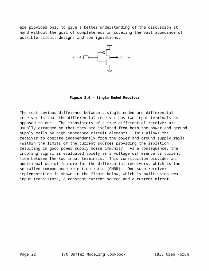
In order to appreciate the operation of differential receivers, it is useful to understand how single ended receivers work. A single ended receiver is usually implemented as transistors connected between the input and ground and/or between the input and power supply terminals. If the receiver is built using field effect transistors (FET), the transistor will usually detect the signal as a voltage that is observed between the input terminal and the power and/or ground supply rails. If the receiver is built with bipolar junction transistors (BJT), the transistor will usually detect the signal as a current flow between the input terminal and the ground and/or power supply rails. In short, the input signal is evaluated with respect to one or both of the supply rails. The following figure illustrates a simple receiver using CMOSFET technology. Please be aware, that the schematics used as illustrations are provided only to give a better understanding of the discussion at hand without the goal of completeness in covering the vast abundance of possible circuit designs and configurations.
Page 14 I/O Buffer Modeling Cookbook IBIS Open Forum
Figure 3.6 – Single Ended Receiver
The most obvious difference between a single ended and differential receiver is that the differential receiver has two input terminals as opposed to one. The transistors of a true differential receiver are usually arranged so that they are isolated from both the power and ground supply rails by high impedance circuit elements. This allows the receiver to operate independently from the power and ground supply rails (within the limits of the current sources providing the isolation), resulting in good power supply noise immunity. As a consequence, the incoming signal is evaluated solely as a voltage difference or current flow between the two input terminals. This construction provides an additional useful feature for the differential receivers, which is the so-called common mode rejection ratio (CMRR). One such receiver implementation is shown in the figure below, which is built using two input transistors, a constant current source and a current mirror.
Figure 3.7 – True Differential Receiver
Half differential receivers are similar in construction, except that the reciever’s input transistors are isolated only from one of the two power supply rails by a high impedance path. Depending on the circuit topology,
IBIS Forum I/O Buffer Modeling Cookbook Page 15
these types of receivers will still evaluate the signal as a voltage difference or current flow between the two input terminals, but the power or ground noise immunity and the CMRR characteristics of such receivers may be inferior to the true differential receivers due to the low impedance path to one of the supply rails.
Figure 3.8 – Half Differential Receiver
Pseudo differential receivers usually consist of nothing more than a single ended receiver connected to each of the two input terminals. The signal on each input terminal is evaluated with respect to the power and/or ground supply rail, and the “difference” signal is obtained by evaluating the logic states of the two independent single ended receivers. This configuration has no supply rail noise immunity or analog common mode signal rejection capability, whatsoever.
Page 16 I/O Buffer Modeling Cookbook IBIS Open Forum
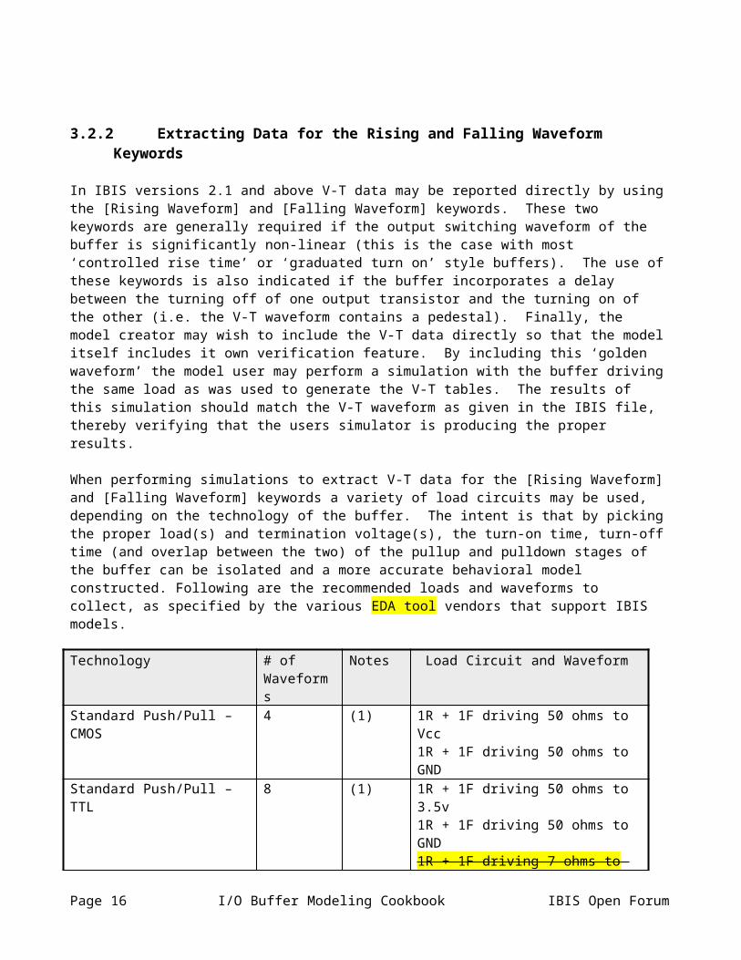
Figure 3.9 – Pseudo Differential Receiver
3.2.5.3 Differential Drivers
In order to appreciate the operation of differential drivers, it is useful to understand how single ended drivers work. A single ended driver is usually implemented as transistors connected between the output and ground and/or between the output and power supply terminals. When the driver is driving low, the output transistor between the output and ground terminals will be turned on, providing a low impedance path from the output terminal to ground. When the driver is driving high, the output transistor between the output and power terminals will be turned on, providing a low impedance path from the output terminal to the power supply rail. In other words, a path is established for current flow between the output terminal and one or the other power supply rails, and if there is a current flow, a voltage will appear on the output terminal with respect to the correcponding supply rail. The following figure illustrates a simple driver using CMOSFET technology.
Figure 3.10 – Single Ended Driver
The most obvious difference between a single ended and differential driver is that the differential driver has two output terminals as opposed to one. The transistors of a true differential are usually arranged so that they are
IBIS Forum I/O Buffer Modeling Cookbook Page 17
isolated from both the power and ground supply rails by a high impedance path (usually a constant current source). This allows the driver to operate independently from the power and ground supply rails (within the limits of the current sources providing the isolation), resulting in good power supply noise immunity. However, there is a major difference between how single ended and differential drivers generate the signal on their outputs. For the discussion that follows, please consider Figure 3.11 below.
Figure 3.11 – True Differential Driver with External Load
In normal operation, the two current sources are designed so that they provide the same amount of constant current. When transistors “A” are turned on, transistors “B” are turned off or vice versa. When transistors “A” are on, the current from the power supply will exit at the non-inverting output terminal (output), and enter back in at the inverting output terminal (/ouput) through the external load resistor and will continue down through the second “A” transistor to the ground rail through the current source on the bottom. When transistors “A” are off and “B” are on, the direction of the current flow is reversed between the two output terminals, and the current will exit at the inverting terminal (/output) and enter at the non-inverting terminal (output). This implies that the signaling of a true differential buffer is established by controlling the direction of the current flow between the two output terminals through the purely differential load placed between them. The amount of output current is independent of the supply voltage (within the normal operation of the current sources). This provides the good power and ground noise immunity. The voltage level of the signal is determined by the output current and the load impedance. Please note that with a purely differential load, providing a current path only between the two output terminals, a voltage will only be measurable between the two output terminals, as the signal will be truly floating with respect to power and/or ground.
Half differential drivers are similar in construction, except that the driver’s output transistors are isolated only from one of the two power supply rails by one current source only. Half of the circuit (two switching transistors and a current source) is usually replaced by two resistors (or equivalent). These resistors are connected to same the supply rail from which the current source was removed. Since these two resistors
Page 18 I/O Buffer Modeling Cookbook IBIS Open Forum
introduce a low impedance path to one of the supply rails, the power or ground noise immunity of such drivers may be inferior as compared with true differential drivers. Please refer to Figure 3.12 below for an illustration of a half differential driver.
Figure 3.12 – Half Differential Driver with External Load
Pseudo differential drivers usually consist of nothing more than two single ended drivers connected to the two output terminals, driven in the opposite direction. The signal on each output terminal is generated as a result of the low impedance path found between the output terminals and the power and/or ground rails. A “differential current” between the output terminals will arise when there is a (differential) load between the two outputs. This current, however, is essencially the result of a voltage divider circuit found between the two power supply rails, and therefore highly influenced by the power supply noise.
IBIS Forum I/O Buffer Modeling Cookbook Page 19

Figure 3.13 – Pseudo Differential Driver Example
3.2.5.4 On-die Termination
In addition to the circuit elements forming the basic driver and/or receiver circuits discussed above, we may some times find additional elements, most often serving the purpose of on-die termination schemes. In general, termination circuits can be grouped into three categories. They can be implemented as pure differential, common mode only, or full termination ( structure or T structure). Please note that the choise of termination style may be independent from the choise of driver and/or receiver style, and they could be mixed. For example, a true differential receiver may have common mode only terminators, or a pseudo differential driver may have a pure differential on-die termination, etc…
A pure differential termination consists of a resistor (or equivalent) connected between the two signal terminals. A common mode only termination consists of resistors (or equivalents) connected between the signal and the power supply or ground terminals. The full termination ( structure or T structure) is a combination of the previous two, using a total of three resistors (or equivalents). As their name indicates it, these termination styles will terminate the transmission lines connected to the signal terminals in the differential mode, common mode, or both modes, respectively.
It should be noted that in the case of half or pseudo differential drivers, the driver design itself may contain circuit elements (resistors or equivalents) which act as termination devices. Since these are usually connected to one or the other power supply rail, these circuit elements usually provide termination only for the common mode components of the signal (or noise).
Another reason true differential drivers and/or receivers may have additional circuit elements connected to the signal terminals is to prevent the signal lines from floating freely. This is usually implemented as weak (high impedance) bias generator circuits and/or resistor (or equivalent) networks using high resistance values.
Page 20 I/O Buffer Modeling Cookbook IBIS Open Forum
Please note that even though differential receivers have two input terminals, there are designs in which only one of these terminals are brought out to the pad or the package pin or ball of the product. In these sitations, the second input terminal is usually connected to an internal reference generator. Also, even if both of the input terminals are brought out to the package pin or ball of the device, there are some signaling specifications which define a single ended signaling with an externally generated reference to be connected to the second input terminal of the differential receiver. A variant of this technique is when a group of receivers share a common reference input to reduce the total number of package pins or balls on the product.
3.2.5.5 Differential Buffer Modeling with IBIS
When discussing differential signaling, differential transmission lines, or termination schemes, experienced engineers usually have a good understanding of the terms “common mode” and “differential mode”. The same principles can be applied to differential buffers also. This concept is especially important when we make IBIS models for differential buffers because of the peculiarities of the IBIS specification.
The IBIS specification has a simple mechanism for modeling differential buffers. The [Diff Pin] keyword is provided to allow the model maker to associate two [Model]s as a differential pair. Since the [Model] keyword was designed to model single ended buffers only, strictly speaking, this mechanism is only useful to model pseudo differential drivers and receivers. As discussed in the above sections, pseudo differential models can only describe the electrical relationships between the signal and power supply terminals, and is unable to include any information on what happens between the two signal terminals of a differential buffer.
Fortunately, there are other mechanisms in the IBIS (v3.2) specification which may be used to overcome this limitation. First, we should note that the [Model] keyword has a Model_type subparameter which can be set to “Series” to model series structures found between signal pins. The original purpose for the series model type was to allow the modeling of devices which are in series with a signal path, hence the name “Series”. A [Model] of type “Series” can contain a number of keywords which may be used to describe passive circuits containing various combinations of inductors, resistors and capacitors, as well as the steady state I-V characteristics of non-linear, active devices, such as transistors. A [Model] of type series can be mapped between any two pins listed under the [Pin] keyword using the [Series Pin Mapping] keyword. It is important to note that the IBIS specification does not impose any limitations on the type of pins the [Series Pin Mapping] keyword can reference, and there are no limitations on how many series models can be connected to a single pin. In practical terms this means that a series model can be mapped between any arbitrary combination of POWER, GND, NC, or signal pins, and that a single pin may have multiple series models connected to it, including another [Model] which describes a normal I/O buffer, for example. Considering these aspects of the IBIS specification, we can construct a model as shown in the following block diagram.
IBIS Forum I/O Buffer Modeling Cookbook Page 21
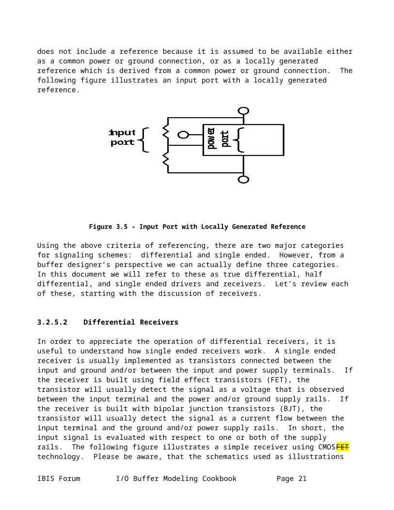
Figure 3.14 – Block Diagram of a True Differential Model using IBIS v3.2 Constructs
The three boxes in this schematic illustrate how the common and differential mode characteristics of a differential buffer can be modeled with IBIS constructs. This arrangement can be applied to true differential, half differential, and pseudo differential buffers equally well. (In the case of the pseudo differential buffers the box labeled “series [Model]” would not be needed). However, there is an important limitation that we need to be aware of when using this concept. Even though [Model]s of type series can describe passive and active circuit elements, the IBIS specification does not provide any control signals for them. This means that a series model cannot be turned on or off, it is considered to be in a static condition throughout the entire simulation. The associated [On] and [Off] keywords provide only a static selection mechanism which cannot be changed during a simulation. For this reason, we can only model differential drivers which have static differential characteristics, i.e. the series [Model] can only contain I-V tables but no V-T tables. As we will see it later in this chapter, this does not seem to be a serious limitation in most practical situations, but in case we need to model dynamic differential characteristics in a buffer, we can make use of the new capabilities provided in the external language extensions of the IBIS v4.1 specification.
Please note that due to the lack of a better term, in the remaining part of this chapter we will refer to the two boxes labeled “driver [Model]” as the common mode model, even though a deeper analysis of these models would reveal that from a theoretical point of view this terminology is not entirely correct.
3.2.5.6 Data extraction
Now that we have a high level concept for modeling the common and differential characteristics of a true differential buffers, let’s discuss how the data can be extracted from a SPICE model for each of these building blocks. Even though in many cases the IBIS model maker does have access to the SPICE netlist, and could extract the data for the above IBIS constructs using different techniques, the preferred method for thise data extraction process is one that does not require any editing of the SPICE netlist because, in more complicated designs, it may be difficult to find clear boundaries for the common and differential mode characteristics in the netlist. It turns out that a simple numerical decomposition technique is available to provide the appropriate data
Page 22 I/O Buffer Modeling Cookbook IBIS Open Forum
for each building block. Unfortunately, at the time of this writing the process described in the following sections has not been automated yet, therefore most of these steps will have to be done manually. However, a presentation on the following discussion including some code examples is available at http://www.eda.org/pub/ibis/summits/oct03/muranyi.pdf.
3.2.5.7 Extracting Common Mode I-V Tables
To simplify the text, we will discuss a differential driver in the following section. Everything here will also apply to differential receivers, unless otherwise noted. The I-V table of a driver is usually measured by forcing a voltage on the output of the buffer and measuring the output current while keeping the buffer in the same logic state. However, since we are dealing with a differential driver, we must ask the question: “Which voltage are we talking about, common mode or differential mode?” The correct answer to this question is: “Both”. The added complexity with differential buffers is that the measured current on one of the output terminals may not only depend on the voltage between that terminal and the ground (or power) supply rail (common mode voltage), but it may also depend on the voltage on the other output terminal (differential mode voltage). For this reason a 2-dimentional I-V table is not sufficient to describe the I-V characteristics of a differential buffer. To describe the current (the dependent variable) as a function of two voltages (the independent variables) we must use a 3-dimensional surface plot.
An I-V surface plot can be generated by connecting two voltage sources to the output terminals of a differential port as illustrated in the following figure. The voltage sources are sweept through the necessary voltage range in a nested loop fashion so that a current reading is obtained for all possible voltage combinations. We can actually generate two I-V surfaces with this arrangement, with the current reading obtained from each of the output terminals. Due to the complemetary nature of the outputs, one of the surface plots will correspond to the logic “1” state of the buffer, and the other will correspond to the logic “0” state. For receivers, the surface plots will contain only clamping and/or on-die termination currents. Unless the receiver has asymmetric characteristics, the measurements obtained from the two terminals will be identical.
I p
Sweep V p while
holding V n
Hi
I - V curves I n
Step through
same range as V p
I p
Sweep V p while
holding V n
Hi I - V curves I n
Step through
same range as V p
I p
Sweep V p while
holding V n
I - V curves I n
Step through
same range as V p
Figure 3.15 - I-V Table Extraction Fixture for a Differential Buffer
The raw data of such an I-V surface sweep is shown in the following figure.
IBIS Forum I/O Buffer Modeling Cookbook Page 23
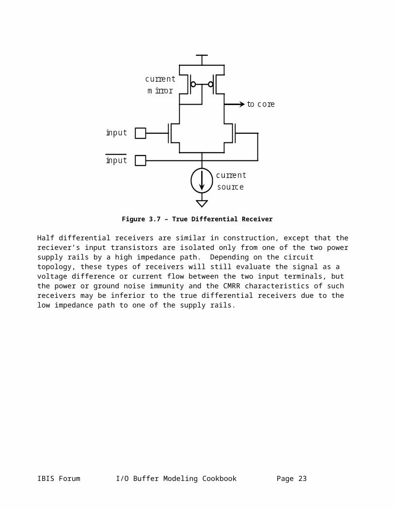
Figure 3.16 - Surface Plots of Raw Data from I-V Sweep of Differential Buffer
The data shown in these plots, being the total current at each output terminal, represents the sum of the common and differential mode currents inside the buffer. It is worth noting that both of these surface plots contain the same exact amount of differential current, because the differential current that flows between the two output terminals is the same regardless of which terminal we are observing it from.
Our next task will be the separation of the common and differential mode currents, to be used in the corresponding [Model]s. In order to do this, we make the assumption that the internal differential current is zero when the differential voltage is zero. While this assumption is true for a resistive path, the question arises whether it can be applied when there are reactive parasitics inside the buffer, such as a capacitor? The answer is a yes, with the condition that we perform a relatively slow sweep during the I-V surface data generation process. A slow voltage sweep corresponds to a low dV/dt, which in turn minimizes the (error) current due to the reactive parasitics. The error or the sweep speed requirements can be calculated from the basic time domain capacitor equation: I = C*dV/dt. For example, a 1 pF parasitic capacitance will yield 1 A of error in our current readings if we sweep the voltage at a 1 V/ms rate. Having said this, we can conclude that the internal differential current is negligible along the equipotential diagonals in the raw data shown above, which also implies that the current reading along these diagonals must be solely due to the common mode characteristics of the driver. Therefore, extracting the current along these yields two 2-dimensional I-V tables, which can be used to fill the [Pullup] and [Pulldown] tables of the common mode [Model]s. These I-V tables are illustrated in the next figure.
Page 24 I/O Buffer Modeling Cookbook IBIS Open Forum
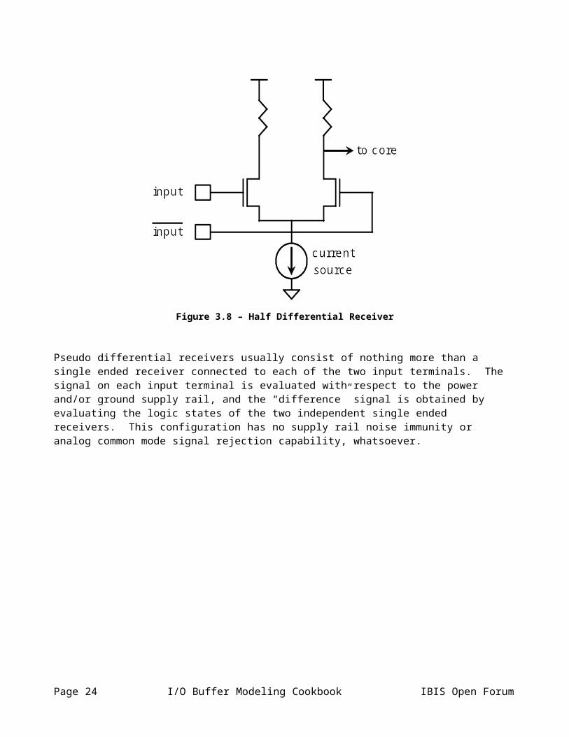
Figure 3.17 - I-V Curves of Common Mode Characteristics of Differential Buffer
3.2.5.8 Extracting the differential mode I-V surfaces
Since the raw data we obtained from the I-V sweep contains the sum of the common mode and differential mode currents, we need to find a way to extract the differential mode current to be used in the series [Model] which will describe the differential characteristics of the buffer. Based on the above discussion, we know that the equipotential diagonal of the surfaces contain nothing but the common mode current. In order to eliminate this common mode component, we just need to perform a vertical translation (shifting) of the surfaces so that their equipotential diagonal becomes zero. This process is similar to summation with a constant, except that the constant is changing for each row in the data matrix (corresponding to the value found in the diagonal for that row). The result of this operation is shown in the next figure.
Idiff = 0Idiff = 0Idiff = 0Figure 3.18 – Differential Current Plot of Output Current versus P and N Voltage
Notice that the two surfaces shown in this figure are identical, because they represent the same differential current flowing between the two output terminals. One of the surfaces shows the current as observed at one of the terminals, and the other surface shows the current as seen at the other terminal. Either one of these surfaces can be used as data for the series [Model], but in order to make this data IBIS compliant, we will first need to reformat it.
IBIS Forum I/O Buffer Modeling Cookbook Page 25

If the surface plot represents the I-V relationship of a linear device, such as a resistor, its shape will be completely flat, tilted in the direction of the diagonal that is perpendicular to the equipotential diagonal. In this case we can reduce the entire surface to a single number, which is the slope of this tilt, and we can use this number as a resistance value for a resistor that is placed between the two output terminals. This differential resistor can be easily modeled using the [R Series] keyword in the series [Model].
If the suface plot exhibits non-linearities we have two keyword options, depending on which way the non-linearities are oriented. If the non-linearity is only a function of the differential voltage, i.e. the curvature of the surface goes only in the direction of the diagonal that is perpendicular to the equipotential diagonal, then we can make use of the [Series Current] keyword in the series [Model]. To fill in the I-V table of this keyword, we just extract the current along this diagonal from the surface plot.
If the surface plot contains non-linearities including voltage dependencies that include common mode voltage, we will have to use the [Series MOSFET] keyword. The IBIS specification states that this keyword can have up to 100 I-V tables. These I-V tables correspond to 100 slices on the surface plot. The keyword also assumes a voltage symmetry along the equipotential diagonal. The symmetry implies that the two halves of the surface are a mirror image of each other along the equipotential diagonal, and imposes certain limitations regarding the freedom in the shape of the surface. The following figure shows an example in which the above surface was sliced to yield 18 I-V tables for the [Series MOSFET] keyword.
IBIS [Series MOSFET] tables
0.0E+00
5.0E-04
1.0E-03
1.5E-03
2.0E-03
2.5E-03
3.0E-03
0.00 0.50 1.00 1.50
Vtable
Ids
Vds=0.0Vds=0.1Vds=0.2Vds=0.3Vds=0.4Vds=0.5Vds=0.6Vds=0.7Vds=0.8Vds=0.9Vds=1.0Vds=1.1Vds=1.2Vds=1.3Vds=1.4Vds=1.5Vds=1.6Vds=1.7Vds=1.8
Figure 3.19 - Plots of Various Vds Values for a [Series MOSFET] Buffer
A tradeoff between accuracy and simplicity is also possible regarding the selection of the appropriate keyword for the series [Model]. The model maker may choose to use the simple [R Series] keyword for the series [Model] if the non-linearities in the differential surface are negligible, or not significant enough to be considered for the model being made. It will be up to the model maker to find the appropriate technique to
Page 26 I/O Buffer Modeling Cookbook IBIS Open Forum
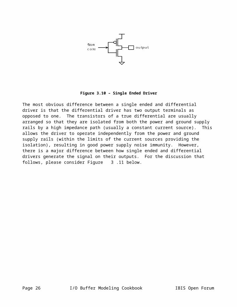
make a best fit representation of the internal differential current surface. Sophisticated mathematical fitting algorithms are available to do this job, but a manual trial and error approach may also be possible.
3.2.5.9 Separating the On-die Termination I-V Tables
As it was shown above (section and/or figure number here), half differential drivers have two resistors (or equivalents) between one of the supply rails and the signal terminals. Since these resistors are never turned off, they can also be considered as common mode on-die terminators, and as such, their I-V characteristics should be placed into one of the clamp tables of the [Model]. Similarly, true differential, or pseudo differential buffers may also contain additional common mode on-die termination resistors (or equivalents), who’s I-V tables should be placed into one of the clamp tables of the [Model]. As with normal single ended [Model]s, care should be taken to avoid the duplication of these currents in the [Pullup] and [Pulldown] I-V tables.
The procedure for this is similar to the corresponding subtraction procedure used for single ended drivers. The I-V characteristics of the driver must be obtained twice, once in the driving mode and once in the 3-stated (high impedance) mode, and the 3-stated I-V table data must be subtracted from the driving I-V table data. The only added complexity in this procedure for differential drivers is that the subtraction is done after the common mode I-V tables have been extracted from the raw I-V surface data.
In addition, extra care should be taken to place the I-V characteristics of the on-die terminations into the appropriate clamp table. As with normal single ended drivers and receivers, if the terminator is connected to the ground rail, its I-V data should go into the [GND Clamp] table, and if the terminator is connected to the power supply rail, its I-V data should go into the [POWER Clamp] table. Also, the model maker must make sure that the termination’s I-V data is not duplicated in both clamp tables. The procedure used for normal single ended buffers applies to differential buffers also regarding the removal of this type of doule counting.
3.2.5.10 Extracting V-T Table Data
First, the reader should understand that this section only applies to driver models since receivers usually do not have any switching characteristics. Also, due to the series [Model] limitations in the IBIS specification, this modeling technique can only account for transient behaviors in the common mode model. Because of this, we will only need to generate V-T tables for the two common mode [Model]s which contain the common mode I-V table data.
The extraction of V-T table data follows the usual techniques applied to single ended buffers. The outputs are connected to the familiar Rfixture and Vfixture load and the buffer is toggled to generate rising and falling waveforms. As usual, for Rfixture we should select a value that is close to the transmission line impedance (common mode) the buffer will drive, and for Vfixture we should use values which correspond to the upper and/or lower DC levels of the signal.
However, in addition to this arrangement, we will need to connect an additional current source between the two output terminals in order to generate correct V-T tables. The purpose of this source is to cancel any internal differential currents inside the SPICE model from which the V-T tables are generated. There are two reasons for having to do this. First, the V-T tables will be used in [Model]s which contain common mode I-V table data only. If the differential currents were not cancelled, we would get I-V and V-T curve mismatch warnings or errors from the IBIS file parser, because the DC levels of the V-T tables would not match the I-V table / Rfixture,Vfixture load line solution in the common mode [Model]. Second, the C_comp compensation algorithm in the [Model] only cancels the C_comp in the common mode model, which does not include the effects of the
IBIS Forum I/O Buffer Modeling Cookbook Page 27
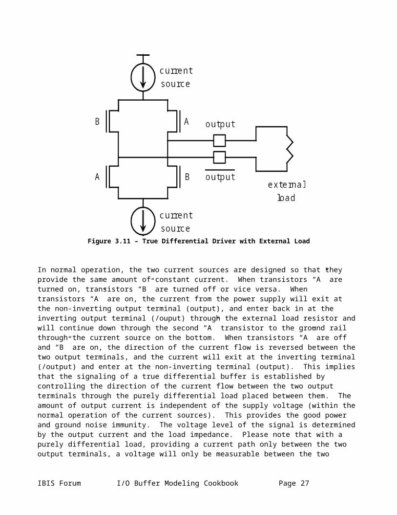
capacitance found between the two output pads (C_diff). If we did not cancel the effects of the differential current caued by C_diff in the V-T tables, the output waveform (i.e. edge rate) of the IBIS model would not be correct. The following figure illustrates this with a schematic.
The cancellation current soure can be implemented many different ways. The implementation may also depend on how the internal differential current is modeled in the series [Model]. In the simplest case, when the series [Model] contains an [R Series] and a [C Series] keywords, one can use the following HSPICE circuit to achieve the cancellation.
Eoutv OutV 0 VOL= 'V(Out_p, Out_n)C_diff OutV 0 C= Value_of_C_diffR_diff OutV 0 R= Value_of_R_diffGcancel Out_p Out_n CUR= 'I(Eoutv)'
The first line of this code is an ideal voltage source which creates a duplicate of the differential voltage found between the two outputs of the buffer. The following two lines contain the differential resistance and capacitance that will be placed into the IBIS file using a series [Model]. The last line of the code above is the current source which is used to cancel the differential current in the SPICE buffer model in order to be able to generate the correct V-T tables for the common mode [Model]s for the IBIS file. If the series [Model] uses the [Series Current] keyword instead of [R Series], a piecewise linear (PWL) current source can be used in place of the resistor in the above circuit. In case the series [Model] uses the [Series MOSFET] keywords, we would technically need a 3-dimensional PWL source which is usually not available in most SPICE simulators. The best way to achieve a cancellation of this type is to use a “dummy” IBIS model instead of the resistor in the above circuit, in which there is a series [Model] that is identical to the series [Model] which will be used for the final differential buffer model.
3.2.5.11 Afterthoughts
The technique described in the previous sections provide a general methodology for making IBIS models for differential buffers, regardless whether they fall into the full, half, or pseudo differential category. In fact, the model maker does not even have to know what kind of differential buffer he or she is working with, the SPICE model of the differential buffer can be treated as a black box for the purposes of this process.
Page 28 I/O Buffer Modeling Cookbook IBIS Open Forum
R=R_fixture
V=V_fixtureR=R_fixture
RiseFall
V-t curves
I=-Idiff R=R_fixture
V=V_fixtureR=R_fixture
RiseFall
V-t curves
I=-Idiff
Figure 3.20 – V-T Table Extraction Fixture for a Differential Buffer
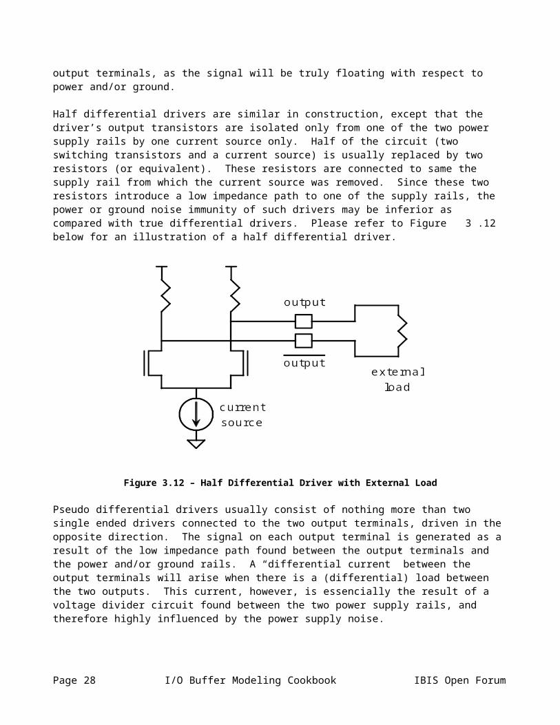
However, it is worth mentioning here, that the series [Model] may not always need to be present in the final IBIS model. In general, the series [Model] will not be needed if there is no internal differential current flowing between the two signal terminals of the buffer. From the discussions above, we know that this is certainly true for pseudo differential buffers. But how can we tell how much internal differential current flows between the two signal terminals of other differential buffers types without looking inside the design? How do we know whether all full or half differential buffers require the series [Model]? Or how can we tell whether there is an on-die termination resistor (or equivalent) between the two signal terminals? One may think that these questions can only be answered with a detailed knowledge of the buffer design. But what if the SPICE model is encrypted, or for some reason we can only treat it as a black box?
Fortunately, the answer to these questions can be found easily by going through the normal process of generating a set of I-V surfaces as described in the previous sections. After the differential I-V surface has been extracted, we just need to find the magnitude of the largest current on it. If the current is in the low A, or nA range, we can conclude that the internal differential current is negligible, and we can safely omit the series [Model] from the final IBIS model. To put this into perspective, a 1 A differential current with a 1 V differential voltage corresponds to a 1 M differential impedance, which will most likely not affect the waveforms in a noticeable way in a 50 transmission line environment.
Also, a case study available at http://www.eda.org/pub/ibis/summits/feb04a/muranyi1.pdf revealed that most true or half differential buffers have practically no internal differential current flow between the signal terminals unless there is a deliberate termination device designed into the buffer between those terminals. This explains why the traditional IBIS modeling approach using two single ended [Model]s as a differential pais worked so well throughout the years.
A word of caution: The technique described above works well for differential buffers built with field effect (FET) output transistors, but may not provide accurate results when the output stage is made out of bipolar transistors. This can be explained with the stronger relationship that exists between the two output transistors’s biasing through their pre-diver circuit.
3.2.5.12 Pre/De-emphasis Differential Buffer Modeling
Most leading edge, high frequency communication technologies use some kind of loss compensation technique in drivers and/or receivers today. Even though the IBIS specification (up to version 4.0) is somewhat limited in modeling such buffers in general, a good number of these buffers in use at the time of this writing can still be modeled with IBIS simple keywords with a reasonably good accuracy. This section will discuss how a special kind of driver family, commonly known as the pre-emphasis or de-emphasis buffers can be modeled with the [Driver Schedule] keyword.
In order to help the reader to understand how these buffers can be modeled, a short overview of the operation of a two-tap pre-emphasis buffer will be given first. The following figure shows the block diagram of such a buffer.
IBIS Forum I/O Buffer Modeling Cookbook Page 29
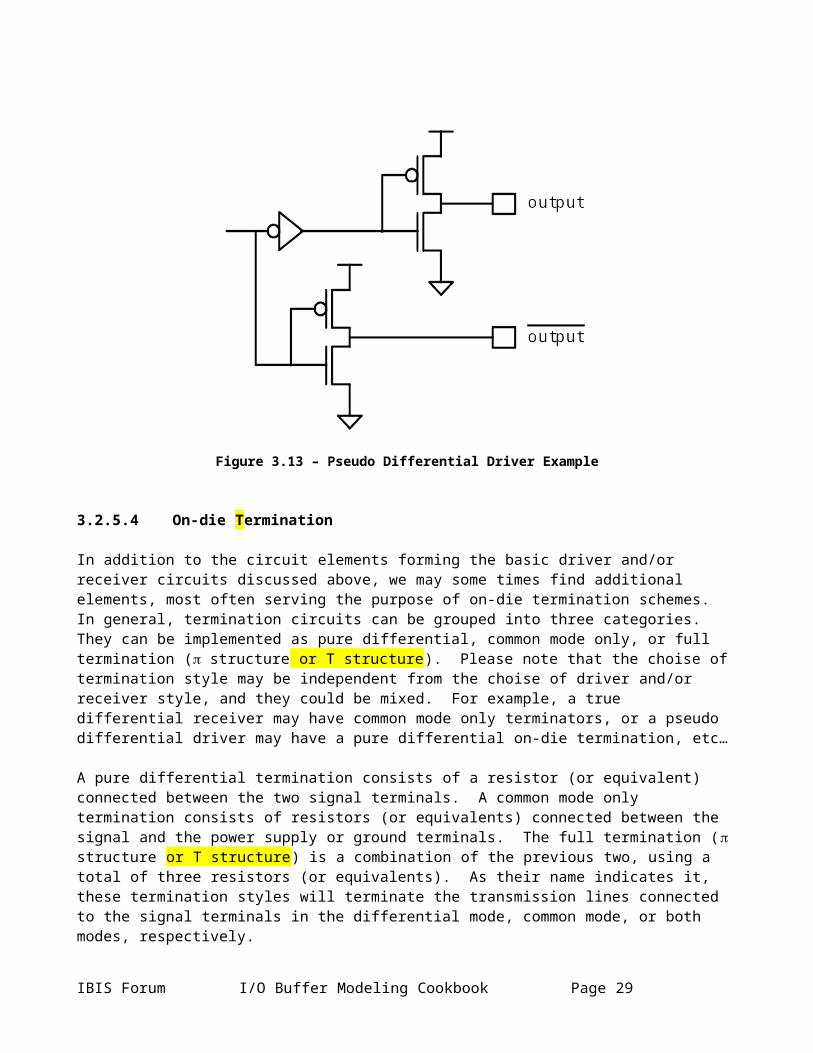
Wired - OR Wired - OR configuration Main (+ & - )
Boost (+ & - )
Input
Emphasis stimulus pattern
TX+ Pad
TX - Pad
D
configuration Main (+ & - )
Boost (+ & - )
Emphasis stimulus pattern
TX+ Pad
TX - Pad
stimulus pattern
Figure 3.21 – Block Diagram of a Two-Tap Differential Buffer Featuring Pre-Emphasis
A two-tap buffer, as its name implies, consists of two buffer blocks. We will refer to them as the “main” and “boost” buffers in this section. In this particular design the boost buffer is used to help the main buffer when the new data bit driven onto the bus is different from the previous bit (0 to 1, or 1 to 0 transition). When the data value remains unchanged (repeated bits), the boost buffer is used to weaken the signal strength by driving an inverted version of the data (to oppose the main buffer). This operation can be achieved simply by applying a one bit delayed and inverted stimulus to the input of the boost buffer.
The [Driver Schedule] keyword provides a useful mechanism for turning individual [Model]s, i.e. buffer blocks on or off. Even though the Polarity subparameter of the scheduled [Model]s is overridden by the top level model (i.e. the scheduled [Model]s cannot have independent polarities), one can still control the polarity of the scheduled [Model]s by choosing the appropriate delay parameters.
For example, constructing an open-drain scheduled buffer using “NA” for the rise_on_dly and fall_on_dly values and zero for the rise_off_dly and fall_off_dly values in the [Driver Schedule] keyword will result in an inverted output, as shown on the waveforms of the next figure.
Page 30 I/O Buffer Modeling Cookbook IBIS Open Forum

Fall_off Rise_off
Rise_off Fall_off
Fall_off Rise_off
Rise_off Fall_off
Fall_off Rise_offFall_off Rise_off
Rise_off Fall_offRise_off Fall_off
Figure 3.22 - Output of a Scheduled Driver Configured as an Inverter
Using this observation, we are now ready to build a pre-emphasis buffer.
3.2.5.13 Building a Pre/De-emphasis BufferThe first step in building a pre-emphasis buffer model is to generate a complete [Model] for its main and boost buffers. In order to achieve this, one must be able to turn off one of these blocks while obtaining the I-V and V-T data for the other. This can be done through enable controls, or by editing the buffer’s SPICE circuit. Either method has its advantages and disadvantages.
According the IBIS specification, only the pullup and/or pulldown I-V tables and their associated V-T tables will go into the scheduled [Model]s. The I-V tables of the clamps and C_comp must be placed into the top level [Model] (see the IBIS specification for more details). Since many of these pre-emphasis buffers also include on-die terminations, care should be taken to avoid duplication of data. Both [Model]’s (main and boost) pullup and/or pulldown I-V tables should contain the difference data (pullup-clamp, and/or pulldown-clamp, where the clamp includes the terminator’s currents). The clamp tables in the top level model should represent the total clamping (and termination) characteristics of the entire buffer. If the clamp I-V tables were generated separately for the main and boost buffers with the SPICE circuit separated, then they will have to be summed together before putting them into the top level [Model]. If they were generated with a complete buffer circuit using enable controls to 3-state the buffer, then one measurement will include the total clamping (and terminaton) characteristics of the buffer.
Once the I-V and V-T tables are done for the top level and scheduled [Model]s, we need to add a [Driver Schedule] keyword to the top level [Model]. This keyword should have two lines, one using the main buffer’s [Model] name and the other using the boost buffer’s [Model] name. The main buffer’s model should have zero
IBIS Forum I/O Buffer Modeling Cookbook Page 31
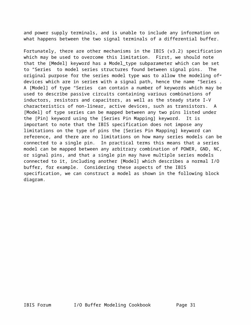
delay values for the rise_on_dly and fall_on_dly parameters, and “NA” for the rise_off_dly and fall_off_dly parameters. This ensures that the main buffer’s [Model] operates in sync with its input stimulus. The delay values for the boost buffer should contain an “NA” for the rise_on_dly and fall_on_dly parameters and a number corresponding to the bit width (clock period) for the rise_off_dly and fall_off_dly parameters.It should be mentioned here that in reality these delays are most often controlled by the clock input of the buffer. However, since models written with IBIS v4.0 or older cannot have any clock inputs, the delay parameter of the boost buffer is basically hard coded into the model. For one, this means that the user of the IBIS model will have to manually change the delay parameters if the clock frequency of the simulation is different from the clock frequency for which the model was made. Second, this may prevent the user of these models to simulate some higher order, clock jitter related effects.
Please note that these concepts may be extended to buffers with more than just two taps. On the other hand, it may not be possible to apply these concepts to each two-tap buffer designs. In order to decide which buffer can be modeled this way one much have a good understanding of the buffer design as well ans the capabilities and limitations of the IBIS specification.
Additional topics to write about:
Symmetric buffers vs. asymmetric differential buffers (two different [Model]s)C_comp problems in pre/de-emphasis buffer modelingTalk about the top level model remaining sections (garbage, or meaningful, parser messages, etc…)Provide links to IBIS summit presentations?
THIS IS FAR AS I GOT NOW!!!
3.2.5.14 Differential Buffer Capacitance (C_diff)
The IBIS C_comp subparameter of a normal single ended [Model] represents the capacitance that is found between the I/O pad and the supply rails of the buffer. For differential buffers it may also be necessary to describe the differential capacitance found between the non-intverting and inverting I/O pads. The IBIS specification does not have a dedicated parameter for this purpose, but one can use the [Series Pin Mapping] keyword with a [Model] that contains a [C Series] keyword to implement this differential capacitance. In the remaining part of this discussion, this differential capacitance will be referred to as C_diff. The following paragraphs will explain how its value can be obtained through simulations or lab measurements.
One way C_comp can be measured for a single ended buffer is by connecting an AC voltage source to its I/O pad and reading the imaginary part of the current in that AC source, as shown in the figure below.
Page 32 I/O Buffer Modeling Cookbook IBIS Open Forum
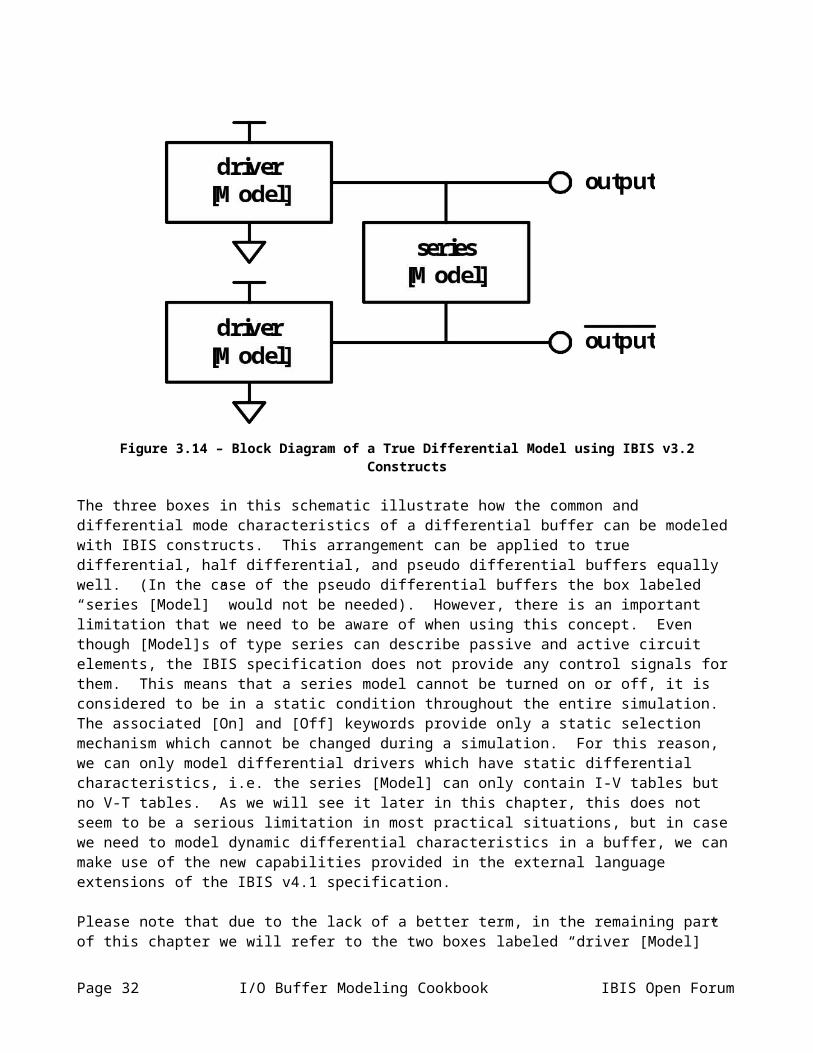
Im(I )
~ V AC
+V DC
Im(I )
~ ~ V AC
+V DC
Figure 3.23 - Fixture for Extraction of C_comp Information
The capacitance can be calculated using the following formula:
C_comp = -Im(IAC) / (2 * * f * VAC),
where Im(IAC) is the imaginary part of the current measured through the AC voltage source, f is the frequency of the AC source, VAC is the AC amplitude of the AC source. Please note that the polarity of the current reading is usually positive when the current flows into the part who’s current we are interested in. Since we are interested in the current flowing into the buffer while measuring it in the AC source, the polarity of the current reading will have to be inverted, which is why there is a negative sign in the above equation. If the capacitance of the buffer is affected by the DC voltage on the output pad (bias), one must also set the DC offset in the AC source to an appropriate value. Since the capacitance of most buffers usually varies with frequency as well as voltage, it is advisable to run a series of simulations in which both of these parameters are swept over a certain range. The results of such simulations can be displayed on a surface plot, as shown in the following figure.
IBIS Forum I/O Buffer Modeling Cookbook Page 33
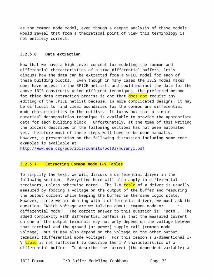
Figure 3.24 - Surface Plot of Buffer Capacitance versus Frequency and DC Bias Voltage
The same technique can also be applied to differential buffers. However, for differential buffers we will need to connect an additional DC voltage source to the second output of the buffer. The voltage of this DC source should be the same as the DC offset of the AC source that is connected to the first output.
Im(IoutP)
Im(IoutN)
~ VAC+VDC
VDC =
Im(IoutP)
Im(IoutN)
~ VAC+VDC
VDC ==Figure 3.25 - Fixture for Extraction of Differential Buffer C_comp
The DC source will have an AC current reading only if there is a reactive path between the two output pads. Therefore, we can use the AC current reading obtained from the DC source to calculate C_diff directly, as shown in the following equation.
Page 34 I/O Buffer Modeling Cookbook IBIS Open Forum
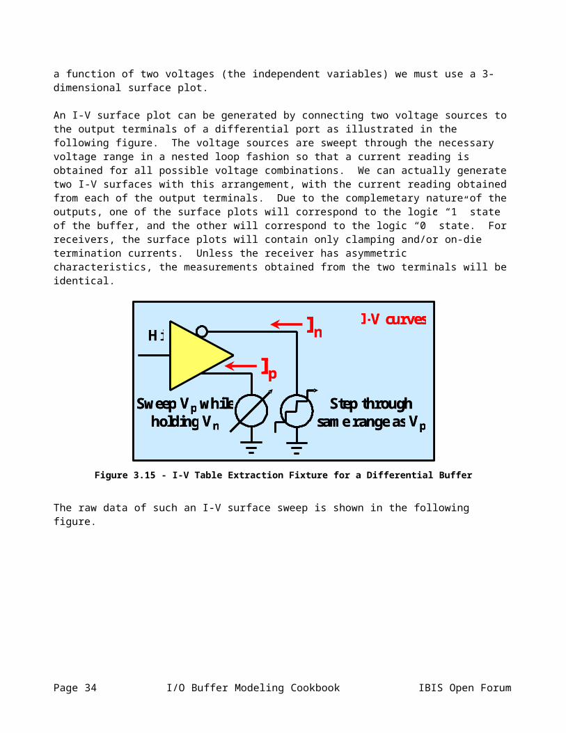
Cdiff = -Im(IDC) / (2 * * f * VAC)
where Im(IDC) is the imaginary part of the current measured through the DC voltage source, f is the frequency of the AC source, and VAC is the amplitude of the AC source.
Please note that the current reading of the AC source will not only include the effects of the differential capacitance (C_diff), but also the effects of the common mode capacitance (C_comp) found between the output pad and the power supply rails. Therefore, to obtain C_comp alone, one must use the difference between Im(IAC) and Im(IDC) from the simulation results generated with the circuit shown above.
C_comp = -( Im(IAC) - Im(IDC) ) / (2 * * f * VAC), orC_comp = ( Im(IDC) - Im(IAC) ) / (2 * * f * VAC)
Please note that due to symmetry, this setup will yield the same results in most cases, regardless of which I/O pad the AC and DC sources are connected to. However, if the buffer is not symmetric internally, it is possible that the C_comp value may not be the same for both outputs. In such cases the above measurement must be repeated with the two voltage sources reversed. The following figure shows a surface plot for C_diff as a function of voltage and frequency for a differential buffer.
Figure 3.26 - Surface Plot of Differential Capacitance versus Frequency and DC Bias Voltage
Since the IBIS specification does not provide mechanisms to describe the buffer capacitance with multi dimensional data, we need to find a way to reduce the vast amount of information generated with the techniques described above. The easiest way to do this is to read the highest and lowest values from the surface plot and put them into the max., and min. places of C_comp or [C Series]. For the typical value, one can simply calculate the average of the maximum and minimum values. To find more meaningful values for these
IBIS Forum I/O Buffer Modeling Cookbook Page 35
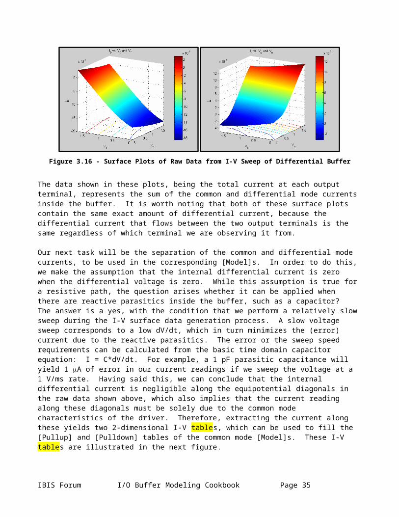
capacitances, one may apply a window to the surface plot using the frequency and voltage range in which the buffer is deigned to operate before reading the maximum and minimum capacitance values from the surface.
3.3 Obtaining I-V and Switching Information via Lab Measurement
You can obtain I-V tables and rise/fall time information from the actual buffer, using the following lab setup: A programmable power supply with an output capable of sinking and sourcing current while
maintaining the required output voltage. The output must be floating. A curve tracer A digital sampling oscilloscope with at least a 4 GHz bandwidth A low capacitance probe, e.g. FET A test fixture used for DC measurements A motherboard or specific test fixture used for transient measurements If available, a thermoelectronic hot/cold plate (a peltier device), to control die temperature
To obtain I-V table measurements, mount the component to be tested in the DC test fixture and connect the power and ground pins of the DUT to the programmable power supply. Attach the hot/cold plate to the component with a very thin layer of thermal grease and adjust the temperature as desired. Wait for the die to stabilize at the desired temperature. Select an output on the DUT in the desired state (high or low) and use the curve tracer to obtain the I-V characteristics of the output.
NotesDuring curve tracing of a tri-statable output, the table contains both the transistor and the diode output characteristics. To obtain tables for the diodes alone, select and curve trace the output in its high impedance state. Buffers containing time-delayed feedback can produce bad results.
Reference the pullup and power clamp data to Vcc, as described in the IBIS specification. You can obtain this data directly by connecting the curve tracer’s negative (reference) lead to the Vcc supply of the DUT, then setting the curve tracer for a negative sweep. Make sure no ground path connects back through the AC line between the component ground and power supply ground. For standard pulldown and clamp diode tables, attach the negative lead to the DUT’s GND supply and use a positive sweep direction. Ensure the supply is floating.
Note that the curve tracer may not be able to sweep the entire range required by the IBIS specification. In this case the model creator must extrapolate the tables to the required range.
Capturing rise/fall time data requires either a specific test fixture or a motherboard to which the DUT can be attached. Rise/fall time measurements require an oscilloscope with at least a 4 GHz bandwidth. Take into account the effect on the rise/fall times of the packaging and capacitive load. Use a probe with extremely low loading, i.e. 1 pf or less, such as a FET probe. The probe grounding should be less than 0.5 inches; i.e., do not use the standard 6 inch probe grounds.
Take an oscilloscope picture of a buffer driving a known load. Then, using the known packaging parameters and measured I-V tables, construct a simulation model of the buffer using a best guess of the rise/fall time. With an IBIS simulator, adjust the rise/fall times in the model until the simulation results match the oscilloscope waveforms. For greater control, lift the pin under test from any load other than the scope probe and simulate with a package and probe model.
Page 36 I/O Buffer Modeling Cookbook IBIS Open Forum
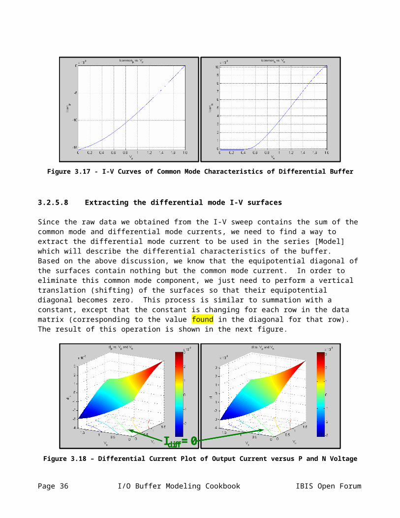
4.0 Putting the Data Into an IBIS File
By this point, the user should have a set of data showing the behavior of the buffer under a variety of environment and design conditions. The data set will include I-V (buffer strength) and, where appropriate, V-T (buffer speed) tables under several conditions. Also, die capacitance information per corner should be available. All this data must now be reformatted into an IBIS model.
The basic objective of any program that converts data to the IBIS format is to properly express the buffer’s behavior in a way “understandable” to IBIS-compatible tools. This involves several specific steps:
basic syntax: representing the data under the proper IBIS keywords data checking: making sure the data is not self-contradictory data limiting: fitting the data within the IBIS size constraints redundancy prevention: ensuring that design aspects are not improperly “double-counted” under
separate IBIS keywords
The following sections detail the specifics behind these steps.
The remainder of the document describes a bi-directional buffer – one capable of both driving a signal into a load and also receiving a signal from an outside world. However, many other buffer types exist; where appropriate, the differences in treatment needed for these other types will be described.The authors assume that the user is interested in either using a currently-available tool to convert data to IBIS format or is trying to perform this task himself. Several software tools exist to ease IBIS data conversions. These include S2IBIS3 (SPICE2IBIS3), a free SPICE-based conversion tool available through the IBIS Open Forum website.
4.1 Basic Syntax: Keywords and Their Definitions
An IBIS file consists of three parts, with an optional ‘external’ package description. The three parts are:1. general information about the file itself and the component being modeled 2. the component’s name, pin-out and pin-to-buffer mapping3. behavioral descriptions of each unique buffer design in that component
Note that an IBIS file can contain a description of more than one component (i.e. parts 2 and 3 above can be repeated several times within one IBIS text file). For more information refer to the description of the [Component] keyword in the specification.
4.1.1 IBIS File Header Information
The first section of an IBIS file contains basic information about the file itself and the data in it. This section includes the following keywords:
Keyword Required? Description[IBIS Ver] Yes What version of IBIS this file uses.[Comment char] No Change the comment character. Defaults to the pipe (|) character[File Name] Yes Name of this file. Remember that all file names must be lower case.
The file name extension for an IBIS file is .ibs[File Rev] Yes The revision level of this file (or model). The specification contains
IBIS Forum I/O Buffer Modeling Cookbook Page 37

guidelines for assigning revision levels. [Date] No Date this file was created[Source] No The source of the data in this file. Is it from a data book? Simulation
data? Measurement?[Notes] No Component or file specific notes. Please see the discussion below.[Disclaimer] No May be legally required[Copyright] No The files copyright notice
Table 2 – IBIS File Header Keywords
The use of these keywords is self-explanatory. Note that while the [Date], [Source], etc. keywords are not required, there use is strongly recommended. The [Notes] keyword is especially valuable, in that the model creator can include in the IBIS file such information as:
Specific model and simulator use information. For example, if the file is marked as IBIS revision 2.1 the [Notes] keyword may specify what specific 2.1 features a simulator must support. Specific model use requirements or caveats may also be described here.
Information on SSO conditions. Under what switching conditions (i.e. how many SSOs) were the minimum, typical and maximum corners derived? Was the buffer’s Tco taken under the same conditions (it should have been)?
Additional package modeling information may be included The models validation level may also be described
4.1.2 Component and Pin Information
This section of an IBIS file is where the ‘data book’ information regarding the component’s pinout, pin to buffer mapping, and the package and pin electrical parameters are placed.
Keyword Required? Description[Component] Yes The name of the component being modeled. Standard practice has
been to use the industry standard part designation. Note that IBIS files may contain multiple [Component] descriptions.
[Manufacturer] Yes The name of the component manufacturer[Package] Yes This keyword contains the range (minimum, typical and maximum
values) over which the packages’ lead resistance, inductance and capacitance vary (the R_pkg, L_pkg and C_Pkg parameters).
[Pin] Yes This keyword is where the pin to buffer mapping information is put. In addition, the model creator can use this keyword to list the R, L and C data for each individual pin (R_pin, L_pin and C_pin parameters).
[Package Model] No If the component model includes an external package model (or uses the [Define Package Model] keyword within the IBIS file itself) this keyword indicates the name of that package model.
[Pin Mapping] No This keyword is used if the model creator wishes to include information on buffer power and ground connections. This information may be used for simulations involving multiple outputs switching. Please see section 4.5.5 for instructions on using this keyword.
[Diff Pin] No This keyword is used to associate buffers which should be driven in a complementary fashion as a differential pair. Please see section 4.5.7 for instructions on using this keyword.
Table 3 – IBIS Component and Pin Information
Page 38 I/O Buffer Modeling Cookbook IBIS Open Forum

Again, these keywords are pretty well explained in the specification. Note that for some components the required keywords [Component], [Manufacturer], [Package] and [Pin] are all that are needed to build the model. The [Pin] keyword is where the pins of the component are defined, and each of the buffer models created are mapped to specific pins. As described in the specification, there must be a buffer model (as called out by the [Model] keyword) for each non power/ground/no-connect pin.
R_pkg, L_pkg and C_pkg are the overall (min and max) values of the package’s resistance, inductance and capacitance. The numerically largest values of R, L and C are listed as the ‘max’ values, while the numerically smallest values of R, L and C are listed as the ‘min’ values.
A subtlety of the IBIS specification for revision 4.0 and previous versions is that buffer pads are implicitly created through the [Pin] keyword. In other words, a “bijective” or one-to-one correspondence is assumed between component pins and die pads, though no explicit die pads are named. Package models are assumed to connect these two points. While convenient, this assumption effectively prohibits package definitions involving a single pin and multiple die pads, or a single die pad and multiple pins, under IBIS versions below 4.1.
4.1.3 The [Model] Keyword
The [Model] keyword starts the description of the data for a particular buffer. While a buffer model can appear quite complex, most buffers can be described using just a few of the parameters and keywords.
4.1.3.1 Parameter Section
A model description starts with the user specifying a few basic parameters. These parameters tell the simulator what type of buffer the model represents, and include some ‘data book’ characteristics of the buffer that enable simulators to do automatic error checking.
[Model] Parameter Required DescriptionModel_type Yes Defines the type of buffer (input, output,
I/O, etc.)Polarity No The polarity of the signals driven by this
buffer (high true or low true).Enable No The polarity of this buffer’s output enable
signal (if applicable)Vinl, Vinh No The buffer’s input logic thresholdsC_comp Yes Buffer input or output capacitance. Note
the discussion on ‘min’ and ‘max’ values of C_comp included in the text below. C_comp_pullup, C_comp_pulldown, C_comp_power_clamp, C_comp_ground_clamp are optional.
Vmeas, Cref, Rref, Vref No Provides the simulator with this buffer’s Tco measurement conditions
Table 4 – IBIS [Model] Subparameters
The IBIS specification gives an extensive list of possible buffer types. Peruse this list carefully to choose your buffer type. Note that if an input or I/O buffer type is chosen the user must specify the Vinl and Vinh
IBIS Forum I/O Buffer Modeling Cookbook Page 39
parameters or verify that the IBIS defaults are correct. The Vinl and Vinh parameter are included so that simulators can flag signal integrity violations and perform timing calculations. In addition, all output or I/O type buffer models should include the Vmeas, Cref, Rref and Vref parameters. Including these parameters allows a simulator to do board level timing calculations.
The C_comp parameter specifies the buffer’s input, output or I/O capacitance and can have a typical, minimum and maximum value. Note that when constructing the IBIS file the numerically largest value of C_comp is listed as the ‘max’ value while the numerically smallest value of C_comp is listed as the ‘min’ value. C_comp min and max values do not necessarily correlate with the min and max conditions under which the I-V and switching data was gathered. C_comp represents only the capacitance of the transistors, die pad and on-die interconnect for an individual buffer. It does not include package capacitance.
C_comp is best generated using one of three methods: performing an AC or frequency sweep analysis of the buffer placing a resistive load at the output and calculating the RC charging or discharging time in a
transient analysis driving the pad using a voltage source and dividing the source current by the dV/dt
Note that C_comp, properly understood, is frequency- and voltage-dependent. The die capacitance – in addition to the overall impedance – of a buffer may change as the operating period increases or decreases. The IBIS model C_comp should be generated at the most likely operating frequency of the buffer.
4.1.3.2 Temperature and Voltage Keywords
Once the basic buffer type and data book parameters have been specified the temperature and voltage ranges over which the buffer operates is given by the following keywords.
Keyword Required? Description[Temperature Range]
No The temperature range over which the min, typ and max I-V and switching data has been gathered. If not specified then 0, 50 and 100 degrees C is assumed.
[Voltage Range] Yes The range over which Vcc is varied to obtain the min, typ and max pullup and power clamp data.
[Pullup Reference][Pulldown Reference][POWER Clamp Reference][GND Clamp Reference]
No Allows the user to specify alternate references (i.e. voltage rails) for any of the four I-V tables.
Table 5 – IBIS [Model] Temperature and Voltage Keywords
The [Temperature Range] keyword has a format different than keywords and subparameters such as C_comp. Note that the ‘min’ and ‘max’ temperature values listed in an IBIS file correspond to the conditions under which the ‘min’ and ‘max’ I-V and switching data was taken. For example, if the minimum (weakest drive, slowest edge) data was taken at 85 degrees C, and the maximum data were taken at 0 degrees C, then ’85’ would be entered in the ‘min’ column and 0 would be entered into the ‘max’ column. Note that these
Page 40 I/O Buffer Modeling Cookbook IBIS Open Forum
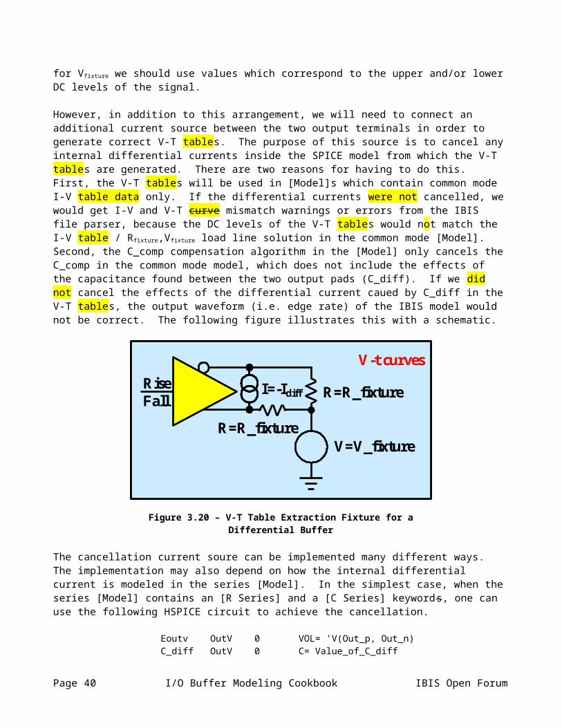
conditions may be different for different technologies; for example, weak or slow CMOS buffer behavior may be found at high temperatures while weak or slow BJT buffer behaviors will more likely found at low temperatures.
The [Voltage Range] keyword specifies the range over which Vcc is varied to obtain the min, typ and max conditions. In addition, this keyword supplies the default voltage reference value for the pullup and power clamp I-V tables. Normally, the [Voltage Range] keyword is all that is required. However, if a buffer uses multiple power supply rails the alternate keywords are used. Very specifically, if the model creator gathers pullup or power clamp I-V data using a voltage reference other than that called out by the Vcc keyword, then the [Pullup Reference] or [POWER Clamp Reference] keywords are used.
The following simple diagram represents the concept behind almost any single-ended IBIS model, regardless of its design complexity.
Figure 4.27 – Conceptual Diagram of Model Keyword Structure
The [Pullup] and [Pulldown] keywords include information on the driver’s strength when it drives high or low, respectively. [POWER Clamp and [GND Clamp] include information on the clamping behaviors of buffers when receiving or in a high-impedance state. While many buffers are much more complex than this diagram indicates, the DC characteristics of the buffer can be neatly fit under these keywords.
The diagram below portrays more detail of the actual connections and electrical relationships between a CMOS buffer and the IBIS [Model] I-V keywords.
IBIS Forum I/O Buffer Modeling Cookbook Page 41
Figure 4.28 – Model Keyword Structure with Added Diode Detail
The drawing illustrates that the bulk or substrate connections of the driving transistors would be connected to the [GND Clamp Reference] in the case of the [Pulldown] or the [POWER Clamp Reference] in the case of the [Pullup]. The transistors’ parasitic diodes will appear in the extracted [POWER Clamp] and [GND Clamp] tables, in addition to any discrete diode structures connected to the buffer pad.
A summary of the I-V keywords is shown below.
Keyword Required? Description[Pulldown] No Data representing the output I-V behavior of a buffer in the logic low
state. This keyword is not used for input buffers. Depending on Model_type, the data may or may not include clamping effects.
[Pullup] No Data representing the output I-V behavior of a buffer in the logic high state. This keyword is not used for input buffers. Depending on Model_type, the data may or may not include clamping effects.
[GND Clamp] No I-V table when the input or output of a buffer is in a high-impedance state and the voltage sweep is ground-relative
[POWER Clamp]
No I-V table when the input or output of a buffer is in a high-impedance state and the voltage sweep is Vcc-relative Table 6 – [Model] I-V Table Keywords
According to the IBIS specification, none of the four I-V tables is mandatory.
Buffers may require different combinations of I-V keyword tables depending on their Model_type. Input buffers include only the [GND Clamp] and [POWER Clamp] keywords, which are used to describe the diode clamping behavior of the buffer. Output only buffers usually contain only [Pullup] and [Pulldown] tables, as their clamping behaviors cannot be isolated from their low or high output states. I/O buffers may drive or receive signals, and so all four I-V keywords are usually present for these types. 3-state buffers, though incapable of receiving signals, can drive or be placed in a high-impedance state where only clamping behaviors are evident. As a result, 3-state buffers also usually contain all four I-V keywords (as I/O and 3-state buffers have identical structures from an IBIS perspective, all recommendations below relating to I/O buffers should be
Page 42 I/O Buffer Modeling Cookbook IBIS Open Forum

assumed to apply to 3-state buffers as well). Other buffer types, such as I/O_open_source, Open_drain and the like, contain combinations of the four I-V keywords appropriate to their driving and receiving capabilities.
Note that the [Pullup] table for a buffer of Model_type Output and [Pullup] data for a buffer of similar design of Model_type I/O will not be identical, if the Output buffer does not contain [GND Clamp] or [POWER Clamp] tables. Output buffers, if no explicit clamp tables are present, have their clamp behaviors included in their [Pullup] and [Pulldown] tables. I/O buffers should include clamp behaviors only in the clamp tables and their [Pullup] and [Pulldown] I-V tables should have had their clamping effects subtracted out to avoid “double-counting” them. When simulation tools use I/O buffer data, they will add the clamp and [Pullup] data together when the buffer drives a high output, and sum the clamps and [Pulldown] data for low driven output. When the buffer receives, the simulation tool will make use only of the clamp tables.
4.1.3.3 I-V Keyword Table Referencing
The I-V data present in the [Pullup], [Pulldown], [POWER Clamp] and [GND Clamp] keyword tables does not use the same reference supply voltages in all cases. If only the [Voltage Range] keyword is used in the relevant model, the [Pullup] and [POWER Clamp] table voltages are assumed to be with respect to the [Voltage Range] values. The [Pulldown] and [GND Clamp] table voltages are assumed, for the same situation, to be with respect to 0 V or ground. In general, this is done to aid in direct comparisons between tables for the same buffer which use different voltage supplies at different corners. An overlay of all three corners of a [POWER Clamp] for a buffer with no leakage and internal terminations, if plotted relative to the supply voltage, would show all three curves passing through the graph origin.
If additional supply keywords – [Pullup Reference], [Pulldown Reference], [POWER Clamp Reference] and [GND Clamp Reference] – are used, [Model] I-V table voltages are shown with respect to their associated reference voltages. For instance, if [POWER Clamp Reference] and [POWER Clamp] are present in a particular [Model], the [POWER Clamp] I-V table voltages are assumed shown with respect to the [POWER Clamp Reference] voltage values.IBIS [Model] I-V table voltage points may be calculated using the formula:
Vtable = Vreference – Voutput
This equation assumes that Vreference and Voutput are ground-relative. For example, imagine a standard 5 V buffer is analyzed using a voltage supply connected to ground. For purposes of generating a [POWER Clamp] table, data is needed from Vcc to 2 * Vcc with respect to ground (see below); here, from +5 V to +10 V. This data would be listed in the [POWER Clamp] table relative to 5 V, spanning a table voltage range from –5 V to 0 V.
4.1.3.4 Ground Clamp
I-V data for the ground-connected diode clamping effects is entered in the [GND Clamp] keyword table. For I/O buffers this is the ground relative data gathered while the buffer was in a non-driving or high impedance state. According to the IBIS specification, the data in table must cover a minimum range of –Vcc to Vcc, measured relative to ground or, if the keyword is present, the [GND Clamp Reference] keyword value for that corner.
As noted in Section 3 above, the raw I-V table for a buffer in a receiving or high impedance state will show both ground and power clamping effects. These effects must be separated in the [GND Clamp] and [POWER
IBIS Forum I/O Buffer Modeling Cookbook Page 43
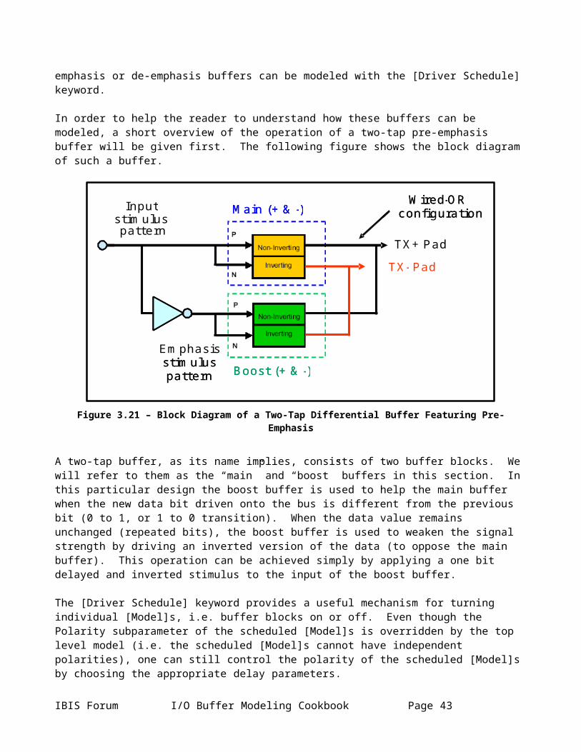
Clamp] tables to ensure that, when the table data is summed again by the simulation tool, no effects are double counted. For the [GND Clamp] table, the raw ground clamp data from lab or simulation extraction should be “cut” at Vcc and the data above Vcc discarded. The table should then be extrapolated to 2 * Vcc for the final I-V table. If power clamp data is properly processed, as will be shown below, this extrapolation will help ensure good simulator behavior when the clamp data is summed.
Figure 4.29 – Graph of [GND Clamp] I-V Table Data
4.1.3.5 Power Clamp
The power clamp I-V data is entered into the [POWER Clamp] keyword table.
As noted above for the [GND Clamp], the [POWER Clamp] data must cover, at a minimum, the range of Vcc to 2 * Vcc (ground-relative). This must be presented in the final table as Vcc-relative, from –Vcc to 0 V. Once the raw high impedance I-V table generated in Section 3 is made Vcc-relative, it should be “cut” at 0 V and the data above 0 V discarded. Again, as with the [GND Clamp], the final table should be extrapolated from 0 V to 2 * Vcc, Vcc-relative, to ensure optimal behavior when the data are summed by the simulation tool.
Page 44 I/O Buffer Modeling Cookbook IBIS Open Forum
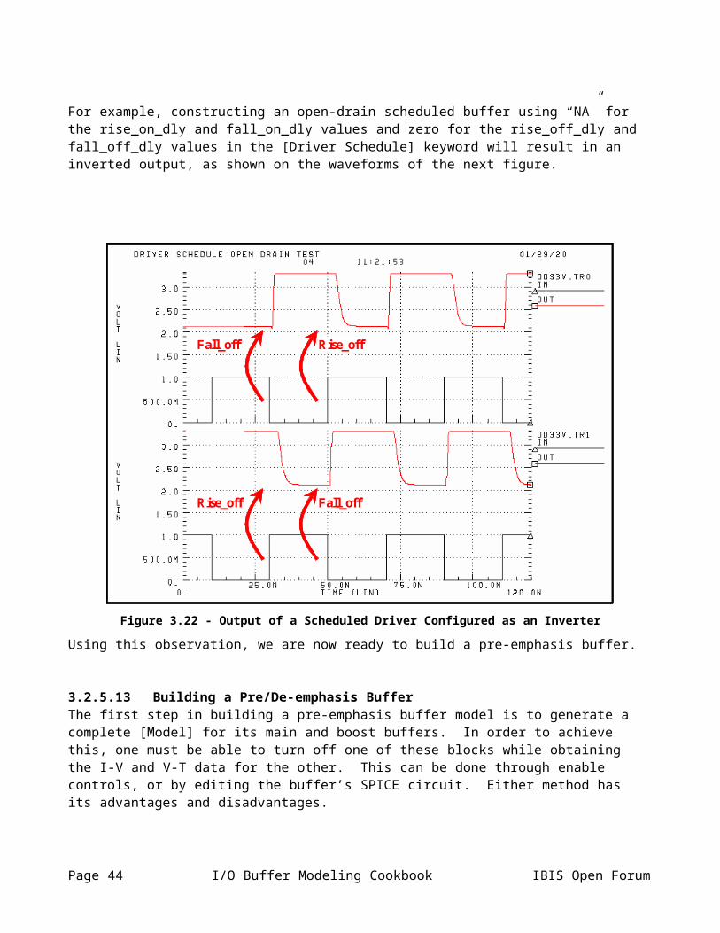
Figure 4.30 – Graph of [POWER Clamp] I-V Table Data after Clamp Subtraction
The relationship of the raw high impedance I-V tables to the final table data is shown graphically below. As described in Section 3, the I-V tables for the high impedance state may be different if the sweeps are performed in different directions (i.e. from low voltage to high voltage and from high voltage to low voltage).
Figure 4.31 – Raw I-V and Extrapolated Final [GND Clamp] Data Graphs
IBIS Forum I/O Buffer Modeling Cookbook Page 45
Figure 4.32 – Raw I-V and Extrapolated Final [POWER Clamp] Data Graphs
4.1.3.6 Pulldown
The [Pulldown] table contains the I-V data gathered while the output or I/O buffer was in the logic low state. To satisfy the minimum requirements of the IBIS specification, [Pulldown] keyword data must cover the range of -Vcc to Vcc *2. If the buffer is of Model_type I/O then first subtract the ground clamp and power clamp currents from the pulldown current and enter the result into the [Pulldown] table (note that the same referencing for the ground and power clamp data should be observed before subtraction). For a 2.0 V buffer, this will result in a pulldown I-V table that resembles the abbreviated table below.
Page 46 I/O Buffer Modeling Cookbook IBIS Open Forum
Table 7 – Pulldown I-V Table (Typical Only)
Below zero volts the buffer’s current may start to increase (become more negative), but then head back towards zero. When tools perform simulations with the buffer in its active state, a simulator sums the ground clamp I-V table with the pulldown I-V table to arrive back at the original pulldown I-V table.
Figure 4.33 – Graph of [Pulldown] I-V Table Data, after Clamp Subtraction
4.1.3.7 Pullup
The [Pullup] table contains the I-V data gathered while the output or I/O buffer was in the high low state. Again, if the buffer is of Model_type I/O, then first subtract the power clamp and ground clamp currents from the pullup current then enter the result into the [Pullup] table (note that the same referencing for the ground and
IBIS Forum I/O Buffer Modeling Cookbook Page 47
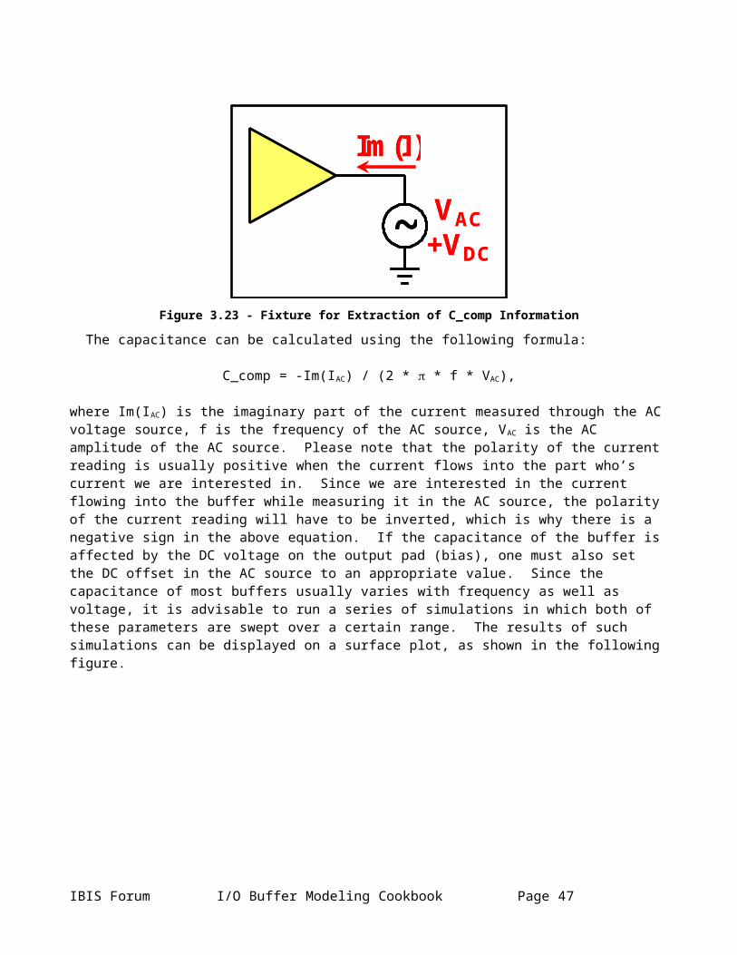
power clamp data should be observed before subtraction). Pullup data must cover the range –Vcc to Vcc *2 in the final table.
Figure 4.34 – Graph of [Pullup] I-V Table Data after Clamp Subtraction
4.1.3.8 Summary of Extraction Ranges
The table below summarizes the ranges over which to present I-V table data in the final IBIS model. Note that the referencing will change from ground and Vcc in the table if [POWER Clamp Reference], [GND Clamp Reference], etc. are used.
I-V Keyword Table Specification Minimum Range Recommended Range[GND Clamp] -Vcc to Vcc (ground-referenced) -Vcc to 2 * Vcc (ground-referenced)[POWER Clamp] 0 to –Vcc, Vcc-referenced in model
(+Vcc to 2 * Vcc, ground-referenced)-Vcc to 2 * Vcc (Vcc-referenced)
[Pulldown] -Vcc to 2 * Vcc (ground-referenced) -Vcc to 2 * Vcc (ground-referenced)[Pullup] -Vcc to 2 * Vcc,Vcc-referenced
(-Vcc to 2 * Vcc, ground-referenced)-Vcc to 2 * Vcc (Vcc-referenced)
4.1.3.9 Extrapolation Errors
One common error when building clamp tables involves extrapolation. Most simulators extrapolate the data points in a table to calculate values beyond the table’s range. For example, examine the following [GND Clamp] table (typical corner only shown):
Voltage Current-1.5 V -120 mA-1.0 V -60 mA0.0 V 0 mA
Page 48 I/O Buffer Modeling Cookbook IBIS Open Forum
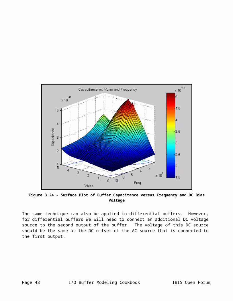
If a simulation tool needs to calculate the circuit response for -2.0 V, it may extrapolate the first two rows in the table to obtain -180 mA at that voltage level. Similarly, if a simulation tool needs the response at 1.0 V based only on this table’s information, it may extrapolate the last two rows in the table to obtain 60 mA at that voltage level.
For most buffers with [GND Clamp] tables where power clamping diodes are described under [POWER Clamp] tables the currents above 0 V are likely to be effectively zero if no on-die termination or leakage is present. Therefore, while the extrapolation below -1.5 V may be appropriate, the extrapolation above 0.0 V as described above is likely not. To ensure correct extrapolation, additional points should be added to the table. In this case, an additional 0 mA point above 0.0 V is necessary, as shown below:
Voltage Current-1.5 V -120 mA-1.0 V -60 mA0.0 V 0 mA0.5 V 0 mA
A similar approach applies to [GND Clamp] or [POWER Clamp] data tables in which on-die termination effects are included (see below). The slope of the curve in the region where diodes are not conducting will be determined by the termination and any extrapolation should be appropriate to the behavior of the termination and the diodes in that region.
Extrapolation can also help to eliminate noise in I-V table data due to subtraction or other computation issues. Small variations in I-V data extracted during different sweeps, for example, may result in large changes in [POWER Clamp] or [GND Clamp] data for the non-clamping regions. If the I-V data cannot otherwise be filtered before inclusion in the IBIS file, extrapolation will prevent distortion in the summed I-V curves used by the simulation tool.
In general, all I-V tables should be generated ensuring that any extrapolation by simulation tools will result in a correct representation of the buffer’s behavior in the extrapolated region.
4.1.3.10 [Ramp] and Waveform Tables
The last piece of information about an output or I/O buffer is the switching information. This information is contained in the following keywords:
Keyword Required? Description[Ramp] Yes Basic ramp rate information, given as a dV/dt_r for rising edges and
dV/dt_f for falling edges.[Rising Waveform]
No The actual rising (low to high transition) waveform, given as a V-T table.
[Falling Waveform]
No The actual falling (high to low transition) waveform, given as a V-T table.
Table 8 – [Ramp] and Waveform Table Keywords
The [Ramp] keyword is always required, even if the [Rising Waveform] and [Falling Waveform] keywords are used. It is important to note that the ramp rate is not the instantaneous slew rate of the output. Instead, it is a number that indicates how long it takes the output transistor structures to switch from one state to another. Specifically, the “ramp rate” as posted in an IBIS file is defined as:
IBIS Forum I/O Buffer Modeling Cookbook Page 49
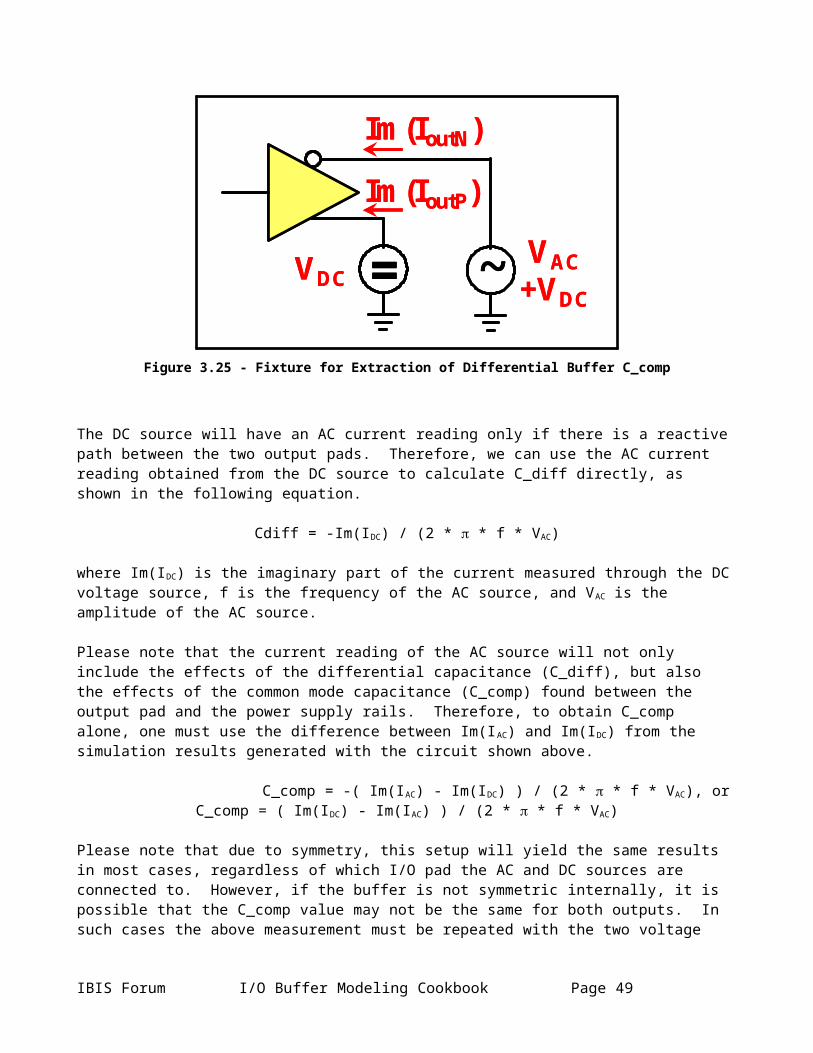
Time taken to swing above voltagedt= 20% to 80% voltage swingdV
Time taken to swing above voltagedt= 20% to 80% voltage swingdV
The dV portion of [Ramp] is not equivalent to the unloaded full swing of the buffer output. Rather, the dV value is the 20% to 80% swing of the buffer when driving into the specified load, Rload (for [Ramp], this load defaults to 50 ohms). For CMOS drivers or I/O buffers, this load is assumed to be connected to the voltages defined by the [Voltage Reference] keyword for falling edges and to ground for rising edges.
For example, if a buffer’s typical falling edge output swings from 3.3 V to 0.8 V for a resistive load of 60 ohms connected to 3.3 V, the dV part of the typical dV/dt_f column of [Ramp] would be 0.6 * (3.3 – 0.8) or 1.5. Rload would be set to 60.
While not checked by the golden parser, the dV portion of [Ramp] should also match the I-V table intercept voltages for the given load. For the example above, where Rload is 60 ohms, the pulldown I-V table should intercept a 60 ohm load line at 0.8 V.
In general, V-T tables under [Rising Waveform] and [Falling Waveform] are preferred to [Ramp] for several reasons. Primarily, V-T data may be provided under a variety of loads and termination voltages, while only one set of [Ramp] data, for only a single resistive load and set of termination voltages, may be provided for any [Model]. Additionally, [Ramp] only provides transition data for devices as they turn on, not as they turn off; V-T tables may be used to describe both types of state changes. Finally, [Ramp] effectively averages the transitions of the device, without providing any details on the transitions themselves. For example, a transition which is ideally linear and another transition which features ledges or “stair-steps” would be described using the same [Ramp] data if the overall time taken by both transitions is the same. All detail of the transition ledges would be lost in the [Ramp] representation. For these reasons, [Rising Waveform] and [Falling Waveform] data should be supplied whenever possible.
Do not reduce dV/dt to a single number.
4.1.3.11 Keywords and Specific Buffer Types
The IBIS standard allows a variety of buffer types to be described with I-V and V-T tables. While the specification is flexible in which tables may be included under any keyword, the following table shows the minimum recommended data for any buffer type.
Page 50 I/O Buffer Modeling Cookbook IBIS Open Forum
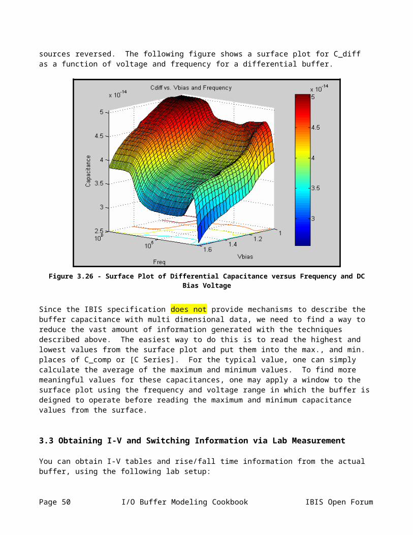
Buffer Type [Pullup] [Pulldown] [POWER Clamp] [GND Clamp] NotesInput n/a n/a Strongly Recommended Strongly RecommendedI/O Strongly Recommended Strongly Recommended Strongly Recommended Strongly RecommendedI/O_Open_drain n/a Strongly Recommended Strongly Recommended Strongly Recommended 1I/O_Open_source Strongly Recommended n/a Strongly Recommended Strongly Recommended 1I/O_Open_sink n/a Strongly Recommended Strongly Recommended Strongly Recommended 1Open_drain n/a Strongly Recommended Optional OptionalOpen_source Strongly Recommended n/a Optional OptionalOpen_sink n/a Strongly Recommended Optional Optional3-state Strongly Recommended Strongly Recommended Optional Optional 2Series Switch n/a n/a n/a n/a 3Series n/a n/a n/a n/a 3Output Strongly Recommended Strongly Recommended Optional Optional 4Terminator n/a n/a n/a n/a 3Input_ECL n/a n/a Strongly Recommended Strongly RecommendedI/O_ECL Strongly Recommended Strongly Recommended Strongly Recommended Strongly Recommended 2Output_ECL Strongly Recommended Strongly Recommended Optional Optional 43-state_ECL Strongly Recommended Strongly Recommended Optional Optional 2
1. Data under "n/a" may be included, if the current is set equal to 02. Functionally similar to I/O3. Special syntax required4. Clamp data may be included, but is added to the required data when the buffer drives
Table 9 – I-V Table Keywords and Buffer Types
Strictly speaking, V-T tables are not required under the IBIS specification. However, for accurate modeling, certain combinations of tables are recommended. These are described in the table below.
Buffer Type Load to Vcc Load to Vss Load to Vcc Load to Vss NotesInput n/a n/a n/a n/aI/O Recommended Recommended Recommended RecommendedI/O_Open_drain Recommended n/a Recommended n/a 1I/O_Open_source n/a Recommended n/a Recommended 1I/O_Open_sink Recommended n/a Recommended n/a 1Open_drain Recommended n/a Recommended n/aOpen_source n/a Recommended n/a RecommendedOpen_sink Recommended n/a Recommended n/a3-state Recommended Recommended Recommended RecommendedSeries Switch n/a n/a n/a n/a 2Series n/a n/a n/a n/a 2Output Recommended Recommended Recommended RecommendedTerminator n/a n/a n/a n/aInput_ECL n/a n/a n/a n/a
I/O_ECLRecommended
(to Vcc - 2)Recommended
(to Vcc - 2)Recommended
(to Vcc - 2)Recommended
(to Vcc - 2) 3
Output_ECLRecommended
(to Vcc - 2)Recommended
(to Vcc - 2)Recommended
(to Vcc - 2)Recommended
(to Vcc - 2) 3
3-state_ECLRecommended
(to Vcc - 2)Recommended
(to Vcc - 2)Recommended
(to Vcc - 2)Recommended
(to Vcc - 2) 3
2. Special syntax required
[Falling Waveform][Rising Waveform]
1. The presence of internal termination s may require adding waveforms in place of "n/a"
Table 10 – V-T Fixtures and Buffer Types
IBIS Forum I/O Buffer Modeling Cookbook Page 51
For example, an IBIS buffer of Model_type “I/O” must contain four sets of I-V tables: [Pulldown], [Pullup], [GND Clamp] and [POWER Clamp]. Similarly, such a buffer must contain, at minimum, a [Ramp] section with both rising and falling dV/dt values. Should V-T data be extracted for this buffer, the data should be included under two [Rising Waveform] and two [Falling Waveform] sections, each containing data for a Vcc-connected load and a ground-connected load.
4.1.3.12 Differential Buffers
Note that the above tables do not include any mention of differential buffers. IBIS has no specific [Model] buffer type parameter to describe differential behavior. Instead, differential buffers are created through a two-step process:
add a [Diff Pin] section for differential inverting and non-inverting pins (see [Diff Pin] below) use the same model for both inverting and non-inverting pins
IBIS can be used to model and simulate differential behaviors through tying two single-ended buffers together and providing input stimuli of opposite polarities. So long as the buffers on the inverting and non-inverting pins in the [Diff Pin] keyword are identical, any model of almost any buffer type containing valid data can be used represent a differential interface.
For example, if a differential driver were to be created and one has single-ended buffer data for the model “TESTMODEL,” one would begin by creating two pins in the [Pin] list, each using the model “TESTMODEL.” The [Diff Pin] section of the IBIS file would show one of these pins as an inverting output and the other as the non-inverting output.
When a simulation is to be performed, so long as the two “TESTMODEL” buffers are provided with input signals which are opposite in polarity, the buffers will act in a differential fashion. Many simulation tools will ensure opposing polarities of input waveforms automatically if the [Diff Pin] keyword is present.
{section incomplete}
If the differential data collection procedures mentioned above were followed, a differential C_comp may be expressed using the [C Series] keyword described below.
4.2 Data Checking
Several data checks are critical to assure final IBIS models that are useful in simulation: data completeness I-V and V-T matching
4.2.1 Data Completeness
Fundamentally, data completeness means having sufficient data to create a useful IBIS model. Users should ensure that the data in their raw data files includes:
I-V data covering the appropriate ranges for all corners I-V data covering sufficient data points to describe buffer behavior I-V data showing behavior for all appropriate input states (high, low, high-Z)
Page 52 I/O Buffer Modeling Cookbook IBIS Open Forum
V-T data covering sufficient data points to describe buffer behavior V-T data (where appropriate) showing complete transitions (settled low to settled high) V-T data (where appropriate) showing two to four or more transitions into a load
See Extracting the Data for more information on generating complete data.
4.2.2 I-V and V-T Matching
For a model of any buffer capable of driving a signal (this includes bi-directional buffers, output-only buffers and the like), one of the most critical concepts is “I-V to V-T matching.” In other words, the settled or DC behavior seen at the start and end of a transition from high-to-low or vice-versa must match the I-V table data for the buffer under the same environmental conditions and under the same load.
The diagram below shows a simple buffer driving a load, connected to ground. The buffer is stimulated to drive from a low output state to a high output state. The voltage-vs.-time waveform for this loaded buffer’s transition is shown, as text.
Figure 4.35 – Diagram of Resistive Load for Rising Waveform
Time V(typ)0.000E+00 0.00E+001.000E-11 2.30E-082.000E-11 4.39E-043.000E-11 2.02E-024.000E-11 3.52E-025.000E-11 6.49E-02{…} {…}
1.800E-10 2.17E+001.900E-10 2.18E+002.000E-10 2.19E+00
Table 11 – Example V-T Table Data for Rising Waveform
If we draw the buffer driver in its most simple form, its behavior can be represented as nothing more than a pullup transistor and a pulldown transistor with connected inputs and connected outputs – an inverter (a CMOS example is shown).
IBIS Forum I/O Buffer Modeling Cookbook Page 53
Figure 4.36 – V-T Table Loading Example
If the signal at the input (“To Core”) is transitioning from high to low, the output will transition from low to high. Under ideal conditions, no current will flow through the pulldown when an external load is grounded and the core is driving high, we can safely exclude the pulldown and treat the buffer as if it consisted solely of the pullup in this situation.
Figure 4.37 – V-T Table Loading Example, Simplified
The voltage of our transient waveform describes the voltage between the resistor and the transistor as the transistor turns on, starting with little to no current flow (off) to maximum current flow (on). When at the end of its low-to-high output transition – when fully on—the transistor is, in essence, a non-linear resistor, which will provide differing current flows dependent on gate voltage and source-to-drain voltage (this should sound familiar from basic electronics, when speaking of transistor table-tracing or bias tables).
Since our gate, source and drain voltages are fixed by the design and the load, we end up with a single current through the transistor when it’s fully on, at the end of our V-T table. This current should match the same current for a load line of 50 ohms drawn across the I-V curve of our transistor. As our I-V curve shows transistor strength and is a DC description of the transistor behavior, the end point of our V-T table – also a DC condition, as the transistor is fully on – should match the I-V for the same load.
Numerically, our example shows the buffer’s transient output to have fully settled at 2.1895 V into a 50 ohm load. This implies a fully-on transistor current of approximately 43 mA, by Ohm’s Law.
Page 54 I/O Buffer Modeling Cookbook IBIS Open Forum
By drawing a load-line of 50 ohms across the (Vcc-referenced) I-V curve for this buffer, we can see that the intercept point is indeed approximately 43 mA.
[Pullup]50 ohm Load Line
Voltage Intercept
Figure 4.38 – [Pullup] I-V Table Data with Load Line Intercept
In this way, we can see that the conditions, loading and output data for both our I-V and V-T are matched to one another. Similar relationships apply to other I-V and V-T tables which may be present in a final IBIS model.
IBIS Keyword Transition Load[Falling Waveform] pulldown turning on Resistor to Vcc[Rising Waveform] pulldown turning off Resistor to Vcc[Rising Waveform] pullup turning on Resistor to GND[Falling Waveform] pullup turning off Resistor to GND
Note: while Vcc and GND are recommended, additionalwaveforms with other load conditions may be usedTable 12 – V-T Table Loading Recommendations
A test of this sort must be conducted when converting any raw simulation data to IBIS format, to ensure that the resulting model will converge properly in system simulation tools.
4.3 Data Limiting
The IBIS 2.1 through 3.2 specifications limit V-T tables to 100 points or rows of data total, for each corner, for the [Rising Waveform] and [Falling Waveform] keywords (this was extended to 1000 points in IBIS 4.0). Similarly, I-V table tables are also limited to 100 points total, for each corner, for the [Pullup], [Pulldown], [POWER Clamp], and [GND Clamp] keywords.
IBIS Forum I/O Buffer Modeling Cookbook Page 55
These limitations mean that some sort of algorithm must be used to select which points from the raw data file are used in the final IBIS model, should the data file contain more than 100 points per corner. Two methods are now in use:
Points selected using a regular interval Points selected using “greatest change” algorithm
The first of these simply “picks” data points at regular intervals over the data set. For example, in a V-T table data set containing 200 points, from 0 ns to 199 ns, the limitation could be met by selecting only even data points plus zero; the sequence would then be 0 ns, 2 ns, and so on.
While this method is simple to implement, it does not discriminate between “meaningful” and “meaningless” data points. If a V-T table has settled by the 50th used data point, the remaining data points will still be selected and added to the IBIS file, though the voltage information will not change.
This failing is remedied by use of a “greatest change” algorithm, where each data point is added to the final IBIS table on the basis of the degree of difference between it and surrounding points. In this way, more points in the final IBIS file will be expended on areas of the tables where large changes take place, such as inflections. Few points will be used on areas where the output does not change, such as the settled voltages before and after a V-T transition.
A visual example is shown below. Note that “flat” or unchanging areas of the graph use few points, while curves and other rapidly changing features are represented with more points.
Figure 4.39 – Data Point Selection Example
Note that the 100-point restriction applies to the number of voltage points in the I-V tables and, for revision 2.1 through 3.2 models, the time points in the V-T tables. Not all I-V current points or V-T voltage points need to be used in the tables, but each table must contain at least two data rows. If necessary, the keyword “NA” may be inserted in the I-V tables for points in any of the corners. The only restrictions on the use of “NA” are:
the starting and ending points for the typical corner in the V-T and I-V tables cannot use the “NA” reserved word
Page 56 I/O Buffer Modeling Cookbook IBIS Open Forum
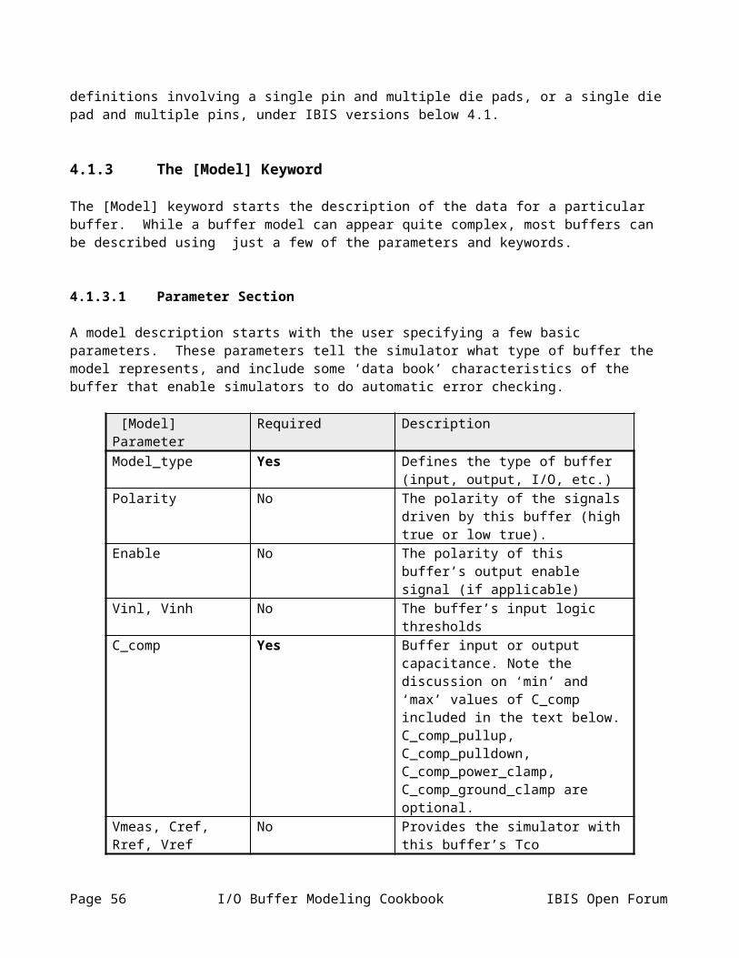
if any data is present in the min or max columns, the first and last points cannot use the “NA” reserved word
This last restriction permits models consisting of typical-only data, where the min and max corners contain only “NA”.
4.4 Additional Recommendations
Several additional procedures should be followed for V-T tables and for buffers with internal termination before the IBIS model is complete. These include:
Adjustment of model data for internal terminations Selection of optimum V-T table windows
4.4.1 Internal Terminations
Internal parallel terminations can affect all four tables of a bidirectional (I/O) buffer model. Most commonly, these terminations are implemented through the use of extra structures on-die which act as resistors, always connected to Vcc and/or ground regardless of whether the buffer drives or receives.
Since the clamp tables are used in an I/O buffer both when driving and receiving, such terminations are best included as part of a clamp table. More specifically, ground terminations should be included with [GND Clamp] data and Vcc terminations with [POWER Clamp] data. This assures that, for example, ground bounce effects will properly affect the [GND Clamp] as opposed to the [POWER Clamp].
For example, Iif a buffer contains an internal ground termination, it can be modeled as shown in the next diagram.
Figure 4.40 – Diagram of I/O Buffer with Internal Termination
Since the [Pullup] and [Pulldown] tables will be created by subtracting the clamp data from the transistor data, then the resistor effects should not appear in these sections and no adjustment to them is necessary. The only change needed to the raw data is to make sure that the resistor’s effects are not “double-counted” with the [POWER Clamp] in addition to the [GND Clamp]. The easiest way to accomplish this is by adjusting the power clamp data before it is clipped for inclusion in the IBIS model.
The “raw” I-V data for the high impedance state, swept relative to ground, will look like the following:
IBIS Forum I/O Buffer Modeling Cookbook Page 57
Figure 4.41 – Raw I-V Table Clamp Data for Ground-connected TerminationThe rules for ground clamp adjustment are:
- clip the ground clamp data at Vcc (ground relative)- extrapolate the ground clamp data at Vcc to 2 * Vcc- clip the power clamp data at 0V (Vcc relative) - subtract current from the power clamp data yuntil the current at 0 V is 0 A- extrapolate the power clamp data at 0 V (Vcc relative) to 2 * Vcc (Vcc relative)
The diagram below shows the raw clamp data taken from simulation or the laboratory.
Page 58 I/O Buffer Modeling Cookbook IBIS Open Forum
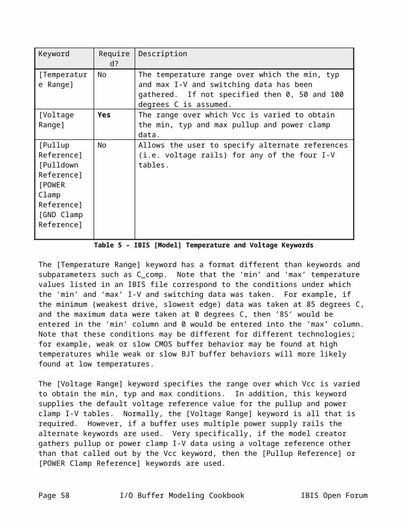
Power clamp before adjustmentFinal [POWER Clamp]Final [GND Clamp]
Vcc(all tables)
Figure 4.42 – Graph of I-V Data for Ground Terminated Buffer in High-Impedance State
Note that following only the minimum IBIS requirements might result in Vcc-connected terminations being included in the[GND Clamp] I-V table of an I/O buffer model. As a result the procedure for adjusting I-V curves based on Vcc-connected terminations is slightly different than that for ground-connected terminations.
As shown in the graph below, the ground clamp current flow at 0 V (ground relative) is negative, implying flow out from the pad.
IBIS Forum I/O Buffer Modeling Cookbook Page 59
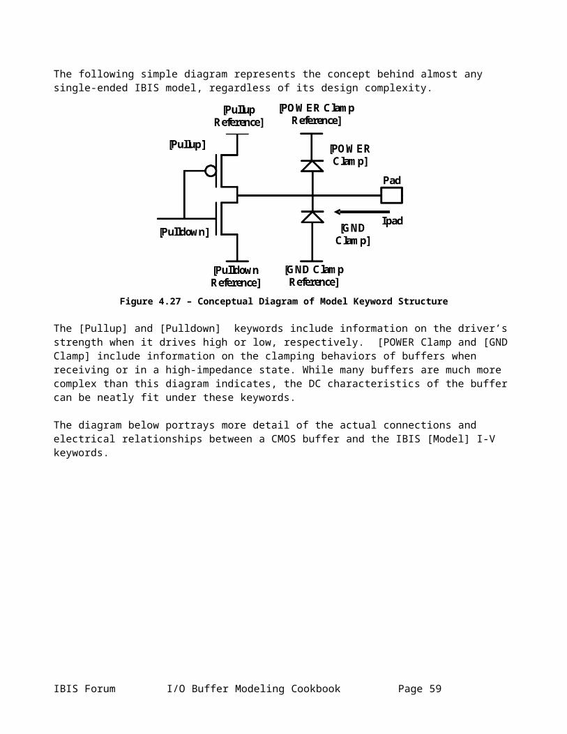
Figure 4.43 – Graph of Power and Ground Clamp I-V Data for Vcc-connected Termination
In order to ensure the Vcc-connected termination is represented solely within the power clamp data,
The rules for Vcc-connected termination adjustment are: clip the ground clamp data at 0 V (ground relative) add current until the current at 0 V is 0 A extrapolate the ground clamp data at the origin to 2 * Vcc clip the power clamp data at Vcc (Vcc relative) extrapolate the power clamp data at Vcc (Vcc relative) to 2 * Vcc (Vcc relative)
Page 60 I/O Buffer Modeling Cookbook IBIS Open Forum
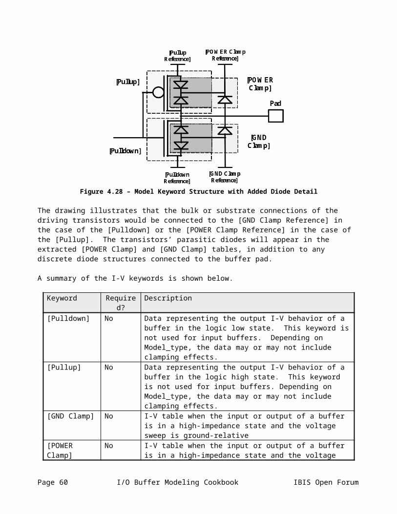
Figure 4.44 – Graph of I-V Data for Vcc Terminated Buffer in High-Impedance State
Other termination types (only on when receiving, only on when driving or receiving specific signal levels) require advanced keywords, as detailed later in the chapter.
Some designs may feature parallel terminations which connect the pad to ground and to Vcc. The treatment of such designs under IBIS is highly simulator dependent.
4.4.2 V-T Table WindowingOne procedure which is not performed by most automated IBIS creation tools is V-T table windowing. While there is no upper limit on the time duration of V-T tables, the transient portion of the waveforms should start and finish within the time dictated by the highest frequency of the buffer (one-half of the period). Several software suites that can accept IBIS models improperly use V-T table data, allowing settled portions to distort buffer behavior when the buffer is driven at higher frequencies.
While not an IBIS requirement, users are strongly recommended to generate V-T tables that are shorter in duration than the pulse width of the highest frequency anticipated on the interface. For example, a signal that is anticipated to drive, at maximum, 100 MHz signals should have a V-T table duration no greater than 5 ns (the period of a 100 MHz signal is 10 ns; such a signal’s pulse width – longest “high time” or longest “low time” – is 5 ns).
4.5 Advanced Keywords and Constructs
Several keywords exist for describing more complex behaviors. The most common of these are described below:
[Model Selector] [Submodel] [Model Spec] [Driver Schedule]
IBIS Forum I/O Buffer Modeling Cookbook Page 61
[Pin Mapping] Series Elements [Diff Pin]
4.5.1 [Model Selector]
The [Model Selector] keyword is a simple means by which several buffers can be made optionally available for simulation at the same physical pin of the component. Normally, each pin of an IBIS pin list references only one buffer, as shown below.
|**************************************************************************|[Pin] signal_name model_name R_pin L_pin C_pin|C10 TXD1 EDX_O434D10 CS EDX_O395||**************************************************************************
In this example, each pin has a unique pin name and separately references a particular buffer model, found later in the file.
[Model Selector] allows a family of buffers to be “attached” to the same pin. The IBIS specification assumes that the simulation tool using the IBIS file will give the user an option of selection which individual buffer within the family will be selected for use in any particular case.
An extension of our example is shown below.
|**************************************************************************|[Pin] signal_name model_name R_pin L_pin C_pin|C10 TXD1 EDX_O43D10 CS EDX_O39AA21 FR# buff_selector_inAB23 AM# buff_selector_out|[Model Selector] buff_selector_out| ADX_O09 1.0V nominal outputADX_O0D 1.7V nominal output|[Model Selector] buff_selector_in| XDX_ISS0 1.0V nominal inputXDX_I550 1.7V nominal input
|**************************************************************************
Here, the names of the [Model Selector] families are substituted in the pin list for the buffer names we would usually expect to see. Later in the file, a [Model Selector] keyword is used, followed by the individual buffers that are part of that selector and a short comment or description of that buffer’s function. In this example, a
Page 62 I/O Buffer Modeling Cookbook IBIS Open Forum
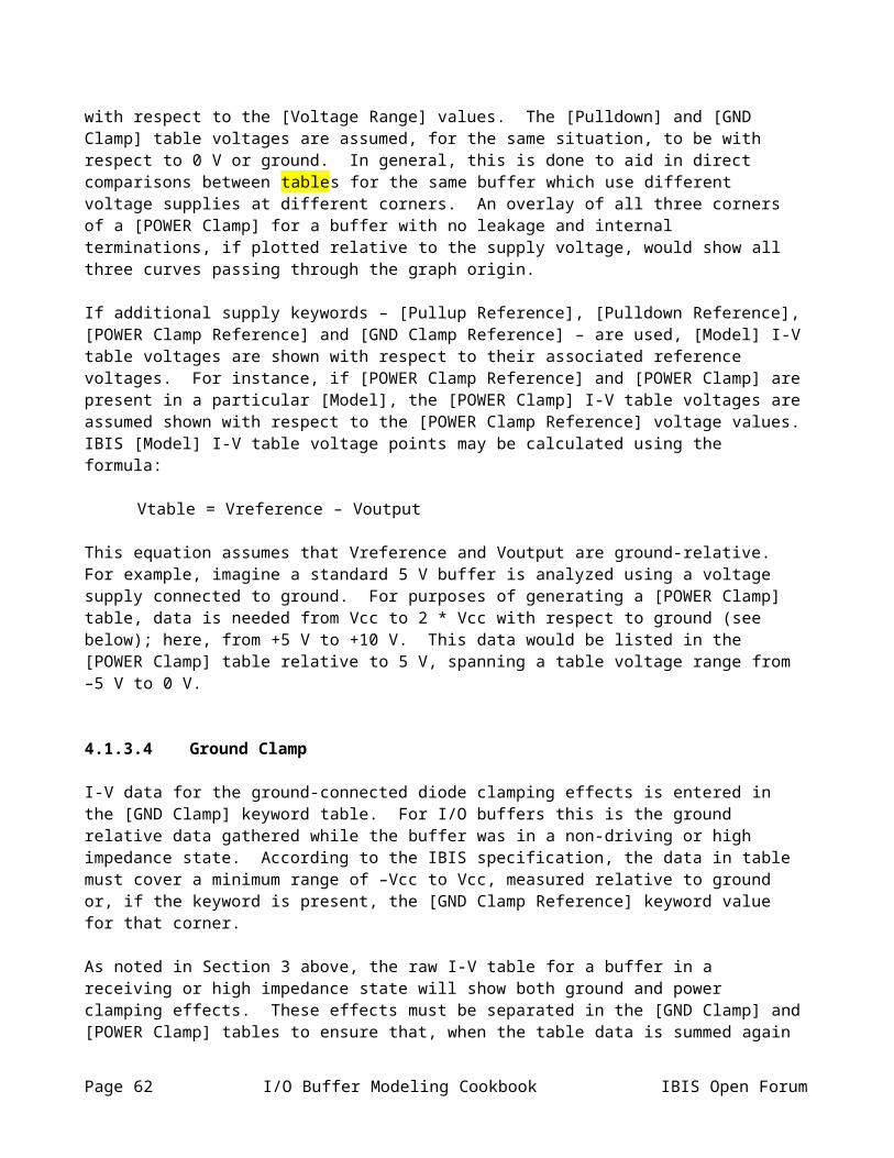
user interested in simulating with pin “AA21” would have to select, through his simulation tool, which of the individual buffers under the [Model Selector] “buff_selector_in” he wishes to use in his simulation.
There is little to no restriction on how many buffers or what buffer types can be used in a particular [Model Selector] section.
4.5.2 [Submodel]
The [Submodel] keyword enables additional buffer features under certain conditions. While not the original intent of the keyword, [Submodel] is commonly used to activate additional clamping circuitry when a bi-directional buffer is receiving, but prevent this circuitry from becoming active when the circuit drives. As the [POWER Clamp] and [GND Clamp] data is present during both driving and receiving states, [Submodel] allows extra driving or clamping behaviors to be described for only some buffer conditions.
Imagine an interface with parallel termination at the receiver. The termination is provided by the buffer itself, by leaving the pulldown transistor on when the buffer is receiving; however, the termination is inactive when the buffer drives. By using a dynamic clamp [Submodel] [GND Clamp], the termination can be included in receiving simulations automatically, without affecting the driver behavior.
The Submodel is called by using the [Add Submodel] keyword. The name and mode of operation must be identified under the [Add Submodel] call. Receiver clamps use the “Non-Driving” mode.
|**************************************************************************[Add Submodel]|Submodel name Mode1550nom Non-Driving|**************************************************************************
The [Submodel] itself is created for this buffer by copying the IBIS [Pulldown] table data exactly and relabeling it as a [GND Clamp]. The [Submodel]’s name must be included here and must match the [Add Submodel] call. Finally, the Submodel_type must be specified; as the termination is a clamp which is active only when the buffer receives, the type is “Dynamic_clamp.”
|***************************************************************************|[Submodel] nomSubmodel_type Dynamic_clamp[GND Clamp]|| Voltage I(typ) I(min) I(max)|1.50000000E+0 -10.85428894E-3 -10.25383174E-3 -11.60286367E-31.45000005E+0 -10.75974107E-3 -10.19728184E-3 -11.48986816E-31.39999998E+0 -10.66339016E-3 -10.14894247E-3 -11.37721539E-3|…2.79999995E+0 34.59529579E-3 37.59065270E-3 31.39221668E-32.84999990E+0 34.65744853E-3 37.69817948E-3 31.43185377E-32.90000010E+0 34.71648693E-3 37.79786825E-3 31.47053719E-3||***************************************************************************
IBIS Forum I/O Buffer Modeling Cookbook Page 63
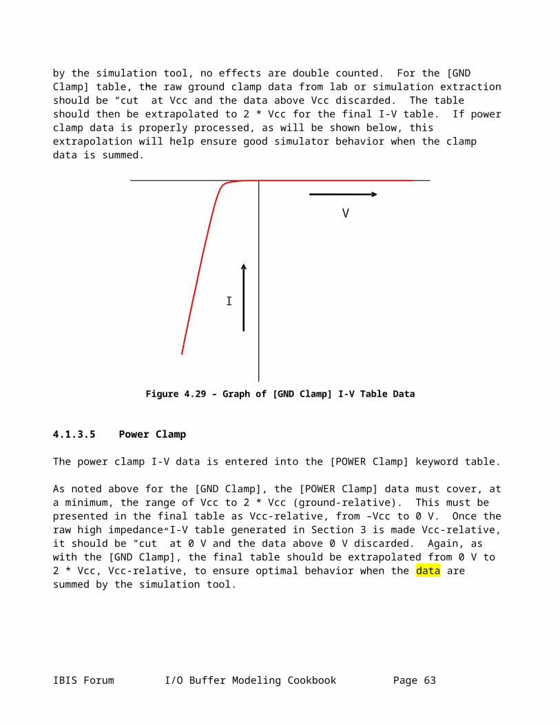
4.5.3 [Model Spec]
The IBIS specification permits users to describe high and low input thresholds, buffer delay fixtures and delay measurement voltages. These values are given under the [Model] keyword, using the Vinh, Vinl, Cref, Vref, Rref and Vmeas parameters, respectively. In some designs, however, the values for these parameters change with corner or supply voltage. The [Model Spec] keyword allows the variations for these parameters to be described in the “typ,” “min,” and “max” format used elsewhere in the model.
In the example below, Vmeas, Vinh and Vinl levels are specified for each of the three model corners.
|***************************************************************************|[Model] standard_bufferModel_type I/O|Vinl = 0.99VVinh = 1.65VCref = 10.000pFRref = 25.0OhmVref = 0.000V|| typ min maxC_comp 3.350pF 3.280pF 3.440pF[Model Spec]|Subparameter typ min maxVmeas 0.9405 0.8921 0.9890Vinh 1.65 1.565 1.735Vinl 0.99 0.939 1.041[Voltage Range] 3.300V 3.130V 3.470V[POWER Clamp Reference] 5.000V 4.750V 5.250V[Temperature Range] 25.0 110.0 0.0||***************************************************************************
4.5.4 [Driver Schedule]
Some applications require that a buffer change its strength or transition speed characteristics at fixed times after input stimulus changes. For example, a buffer may employ a “kicker” or boosted drive strength on its pullup behavior for the first few nanoseconds after a low-to-high transition. Since the buffer effectively has two drive strengths, no single set of I-V and V-T tables can effectively describe its behavior. The [Driver Schedule] keyword enables a buffer model to use or combine the behaviors of several individual models.
The keyword is itself part of a model, usually called the “top-level” model. The parameters of the keyword form a list of the models whose behavior the top-level model schedules (the top-level model is required for the benefit of simulation tools which cannot support the [Driver Schedule] behavior). Each incorporated model can include up to four delay parameters, expressing the delay for pullup and pulldown behavior turning off or on after a rising or falling edge.
|***************************************************************************|[Model] GTL_example
Page 64 I/O Buffer Modeling Cookbook IBIS Open Forum
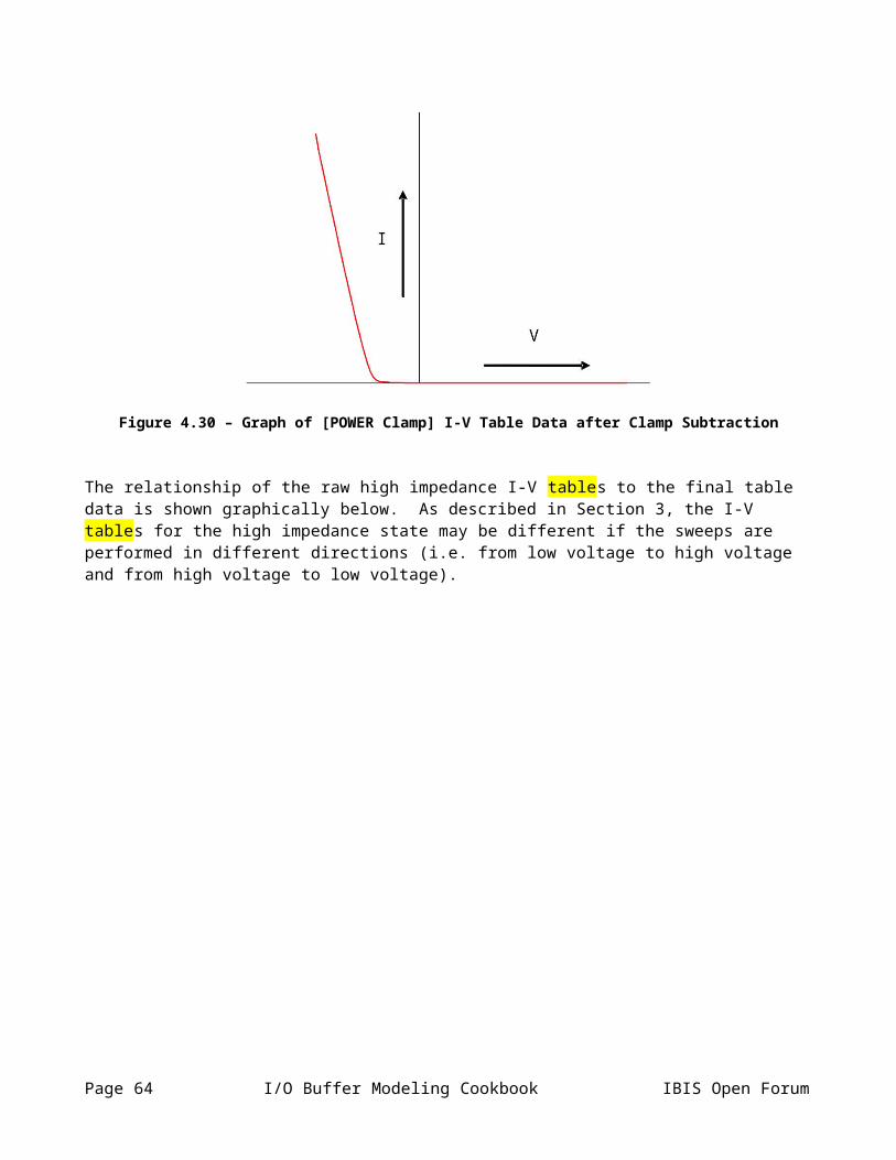
Model_type I/O|Vinl = 800.00mVVinh = 1.20VVmeas = 1.00VVref = 1.50VRref = 50.00OhmCref = 0.00pF|| typ min max|C_comp 2.20pF 1.90pF 2.50pF[Voltage Range] 1.800V 1.650V 1.900V[Temperature Range] 50.0 100.0 0.0||***************************************************************************| [Driver Schedule]|| Model_Name Rise_on_dly Rise_off_dly Fall_on_dly Fall_off_dly| P0_stage 0.0000ns 5.0000ns NA NA N0_stage 0.0000ns NA 0.0000ns NA N1_stage 0.3006ns NA 0.0549ns NA N2_stage 0.5481ns NA 0.1163ns NA ||***************************************************************************
The above example illustrates how the [Driver Schedule] keyword is incorporated into a top-level model, just after the header. In this model, five separate models are scheduled by the “GTL_example” top-level model; these models are named in the first data column.
The second and third columns describe how the scheduled buffers are to behave after a rising edge on an input stimulus. “Rise_on_dly” specifies when the pullup section of the scheduled buffers turns on after the rising edge, while “Rise_off_dly” describes when the pullup turns off. Similarly, “Fall_on_dly” and “Fall_off_dly” specify how long a delay exists between the pulldown turning off or on after a falling input edge.
More specifically, P0_stage turns its pullup on immediately after a rising input edge is detected. The buffer pullup turns off 5 ns after this rising input edge. After a falling input edge, the pulldown of N2_stage will wait 0.11163 ns before turning on its pulldown section. In this way, strong pullup and pulldown behaviors are created slowly, as the independent buffers turn on or off in stages after input edges.
4.5.5 [Pin Mapping]
The [Pin Mapping] keyword contains information on how power supplies are connected to individual buffers or groups of buffers. The [Pin Mapping] format generally resembles the [Pin] format, in that all of the component’s pins are listed by pin name. Each pin name is followed by entries which associate model supplies with particular names.
As an example, note the following component:
IBIS Forum I/O Buffer Modeling Cookbook Page 65
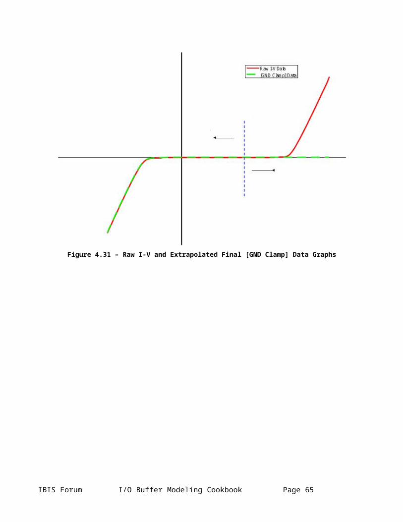
Figure 4.45 – Component Diagram Showing Buffer and Supply Buses
A pin list for a component might resemble the following:
|*********************************************************************[Pin] signal_name model_name R_pin L_pin C_pin1 Driver_33Vclamp1 iobuffer332 Driver_33Vclamp2 iobuffer333 Driver_5Vclamp iobuffer54 NC NC5 VCC3RAIL POWER6 VSSRAIL GND7 VCC5RAIL POWER||*********************************************************************
Page 66 I/O Buffer Modeling Cookbook IBIS Open Forum
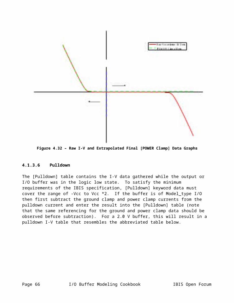
This component includes two drivers which share the same ground supply and use 3.3 V supplies for their pullups, but have different power clamp supplies. [Pin Mapping] can make these relationships explicit.
|**************************************************************************[Pin Mapping] pulldown_ref pullup_ref gnd_clamp_ref power_clamp_ref ext_ref1 VSS VCC3 VSS VCC32 VSS VCC3 VSS VCC33 VSS VCC3 VSS VCC54 NC NC| Supply connections only use pullup, pulldown and ext_ref columns| 5 NC VCC3 | 3.3 V supply pin6 VSS NC | Ground pin7 NC VCC5 | 5.0 V supply pin||**************************************************************************
The first three rows of the [Pin] list above refer to buffers. These I/O buffers have pullup, pulldown, power clamp and ground clamp supply connections. For each buffer pin, the pulldown_ref, pullup_ref, gnd_clamp_ref and power_clamp_ref columns contain the names of rails or buses which connect to the appropriate portions of the buffer.
For example, pin 1 is associated with “Driver_33Vclamp1” which uses the model “iobuffer33.” The pullup of this buffer is connected to the supply rail named “VCC3”, as shown the pullup_ref column for pin 1 of the [Pin Mapping] keyword. Similarly, the buffer “Driver_5Vclamp” has a power clamp which is connected to the supply rail named “VCC5.”
POWER and GND pins are not associated with buffers but are instead the points at which supply buses connect to the pins of the component. In other words, POWER and GND pins in the [Pin] list are assumed to provide supply voltages to the [Pin Mapping] buses and therefore to the component’s buffers. Under the [Pin Mapping] keyword, entries for POWER and GND pins is only to be placed in the second, third (and possibly sixth column). The pulldown_ref column contains the name of the bus to which the GND pin is connected; for GND pins, the pullup_ref column must contain NC. Similarly, the pullup_ref column contains the name of the name of the bus to which the POWER pin is connected; for POWER pins, the pulldown_ref column must contain NC.
For POWER and GND pins, the sixth column, ext_ref, may contain a bus name, to refer to an external reference voltage. If ext_ref contains an entry, the gnd_clamp_ref and power_clamp_ref columns must contain NC.
In the example above, pin 5, a POWER pin in the [Pin] list, carries the VCC3 3.3 V supply voltage. Similarly, pin 7, also a POWER pin, carries the VCC5 5.0 V supply voltage. The ground pin for all buffers is pin 6, a GND pin.
Note that all buses must connect to either a POWER or GND pin. However, buses may be defined without any buffer connections.
Note that the IBIS specification requires that, if [Pin Mapping] is present, EVERY pin from the [Pin] list must be also listed under [Pin Mapping].
4.5.6 Series Elements
IBIS Forum I/O Buffer Modeling Cookbook Page 67
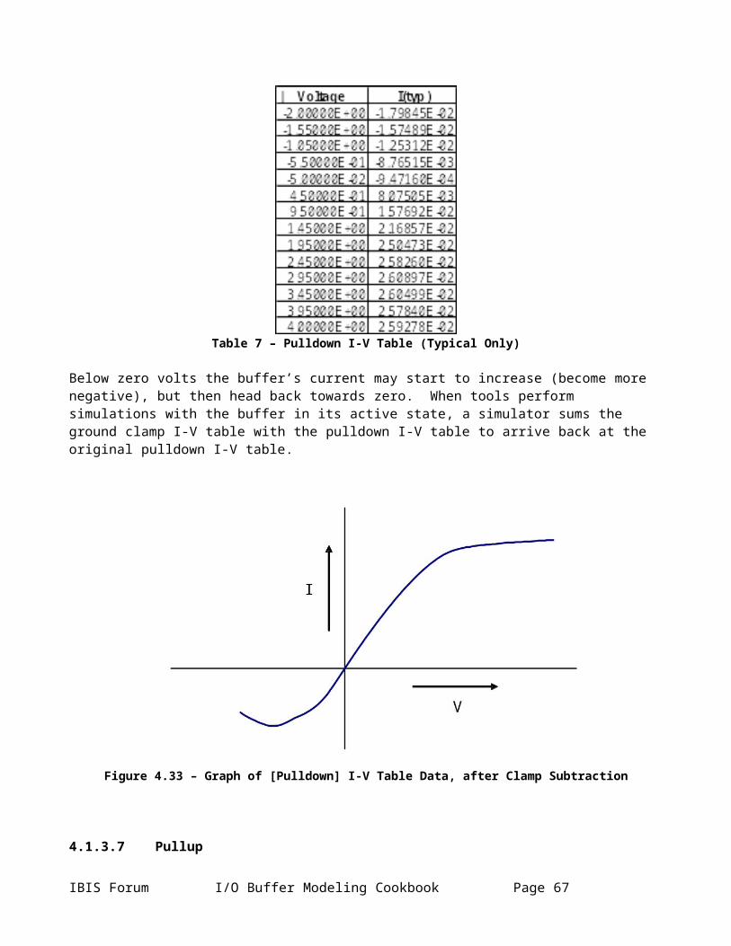
Series elements, or electrical connections between pads, may be described using combinations of the keywords [Series Current], [Series MOSFET], [Series Pin Mapping], [Series Switch Groups] and several others. Series connections may be made between pads to which single-ended buffers are already connected (see Figure 4.46 below). Also, note that the use of any of these keywords does not demand or preclude the use of the [Diff Pin] keyword.
Figure 4.46 – Connection of Single-ended and Series [Model]s
Proper declaration of non-switch series elements involves at least two steps: use of [Series Pin Mapping] to declare the connection (this keyword is usually placed between [Pin]
and the first [Model] keyword) use of a [Model] of Model_type ‘Series’ which includes one or more of the following keywords and
data sets: [Series Current], [Series MOSFET], [R Series], [L Series], [C Series], [Rl Series], [Rc Series], [Lc Series]
Proper declaration of series switch elements involves a more complicated procedure: use of [Series Pin Mapping] to declare the connection (this keyword is usually placed between [Pin]
and the first [Model] keyword) use of [Series Switch Groups] to declare the grouping of enabled states of the switch use of a [Model], of Model_type ‘Series_switch,’ which includes the [On] and [Off] keywords each of
which contain one or more of the following keywords and data sets: [Series Current], [Series MOSFET], [R Series], [L Series], [C Series], [Rl Series], [Rc Series], [Lc Series]
For example, an IBIS file which models an RC circuit that connects two pins of a component would resemble, in part, the following:
|**************************************************************************[IBIS Ver] 3.2 [File Name] rcpath-test.ibs [File Rev] 1.0 [Date] 8/22/2003 [Source] From silicon level SPICE model.[Notes] The following information is for illustration purposes only
Page 68 I/O Buffer Modeling Cookbook IBIS Open Forum
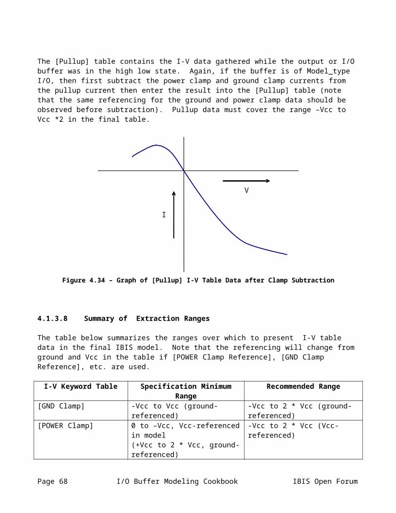
and does not conform to any known device.[Disclaimer] See above. [Copyright] Copyright (C) 2004 Them Corporation| |**************************************************************************[Component] Example_RCSeries[Manufacturer] Them Corporation [Package] | typ min max R_pkg 0.0Ohm 0.0Ohm 0.0Ohm L_pkg 0.00H 0.00H 0.00H C_pkg 0.00F 0.00F 0.00F | |**************************************************************************[Pin] signal_name model_name R_pin L_pin C_pin 1 RC_test Groundclamp 2 RC_test Groundclamp | |***************************************************************************[Series Pin Mapping] pin_2 model_name function_table_group1 2 RCpath| |***************************************************************************[Model] GroundclampModel_type InputPolarity Non-InvertingVinh = 2.0Vinl = 0.8| | typ min maxC_comp 7.0pF 5.0pF 9.0pF | | typ min max [Voltage Range] 5.0V 4.5V 5.5V | [GND Clamp]|| Voltage I(typ) I(min) I(max)|1.50000000E+0 -10.85428894E-3 -10.25383174E-3 -11.60286367E-31.45000005E+0 -10.75974107E-3 -10.19728184E-3 -11.48986816E-31.39999998E+0 -10.66339016E-3 -10.14894247E-3 -11.37721539E-3|2.79999995E+0 34.59529579E-3 37.59065270E-3 31.39221668E-32.84999990E+0 34.65744853E-3 37.69817948E-3 31.43185377E-32.90000010E+0 34.71648693E-3 37.79786825E-3 31.47053719E-3||***************************************************************************[Model] RCpath Model_type SeriesPolarity Non-Inverting Enable Active-High | | typ min maxC_comp 0.0pF 0.0pF 0.0pF |
IBIS Forum I/O Buffer Modeling Cookbook Page 69
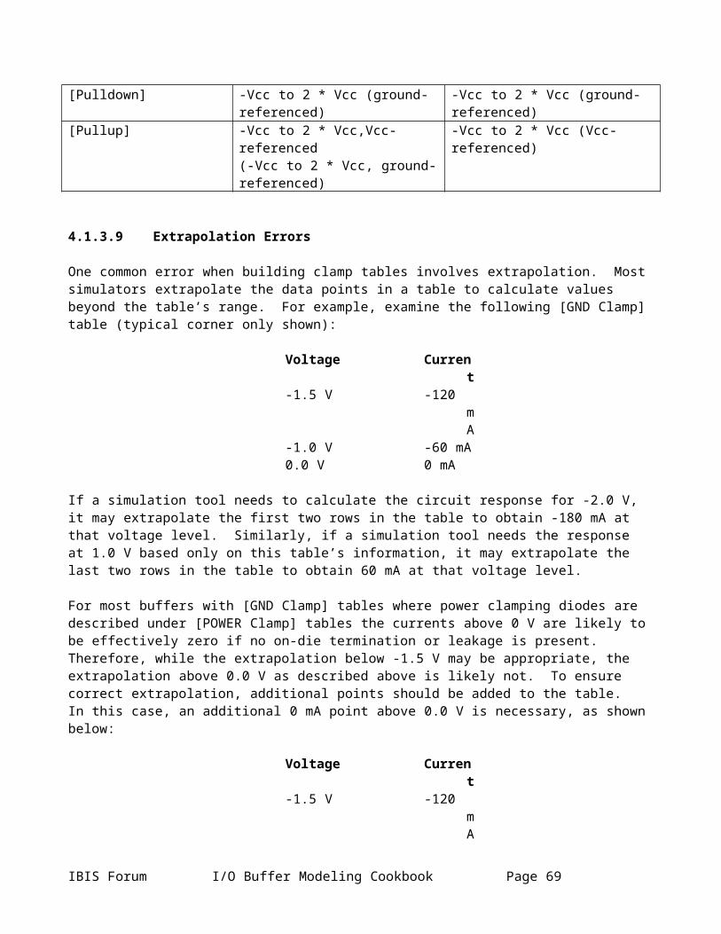
| typ min max [Voltage Range] 5.0V 4.5V 5.5V | |*************************************************************************** | R(typ) R(min) R(max)[Rc Series] 4ohm NA NA|| C(typ) C(min) C(max) [C Series] 50pF NA NA | [End]
In the example above, electrical information is given both for the single-ended behavior of the component’s two pins and for the RC circuit between the pins. The [Rc Series] keyword describes the resistance assumed to exist in series with the capacitance defined by the [C series] keyword.
Similarly, an IBIS file which models a MOSFET that connects two pins of a component would resemble, in part, the following:
|**************************************************************************[IBIS Ver] 3.2 [File Name] mosfet-test.ibs [File Rev] 1.0 [Date] 8/22/2003 [Source] From silicon level SPICE model.[Notes] The following information is for illustration purposes only and does not conform to any known device.[Disclaimer] See above. [Copyright] Copyright (C) 2004 Them Corporation| |**************************************************************************[Component] Example_Switch [Manufacturer] Them Corporation [Package] | typ min max R_pkg 0.00Ohm 0.00Ohm 0.00Ohm L_pkg 0.00H 0.00H 0.00H C_pkg 0.00F 0.00F 0.00F | |**************************************************************************[Pin] signal_name model_name R_pin L_pin C_pin 1 MOSFET_test NC 2 MOSFET_test NC | |***************************************************************************[Series Pin Mapping] pin_2 model_name function_table_group1 2 mosfet 1 | |***************************************************************************[Series Switch Groups] On 1 / Off 1 / | |***************************************************************************
Page 70 I/O Buffer Modeling Cookbook IBIS Open Forum
[Model] mosfet Model_type Series_switch Polarity Non-Inverting Enable Active-High | | typ min maxC_comp 7.0pF 5.0pF 9.0pF | | variable typ min max [Voltage Range] 5.0V 4.5V 5.5V | |*************************************************************************** [On] [Series MOSFET]Vds = 5| Voltage I(typ) I(min) I(max) 5.0V 6.4475 3.8325 9.9875 | Defines the Ids current as a 4.0V 5.075 2.985 7.9325 | function of Vtable for Vds = 53.0V 3.245 1.8675 5.14 2.0V 0.78 0.415 1.275 1.0V 1.31E-09 1.1675E-09 1.4175E-090.0V 0 0 0 |[Series MOSFET] Vds = 3 | Voltage I(typ) I(min) I(max) 5.0V 2.3211 1.3797 3.5955 | Defines the Ids current as a 4.0V 1.827 1.0746 2.8557 | function of Vtable for Vds = 33.0V 1.1682 0.6723 1.8504 2.0V 0.2808 0.1494 0.459 1.0V 4.743E-10 4.203E-10 5.103E-10 0.0V 0 0 0 |[Series MOSFET] Vds = 1 | Voltage I(typ) I(min) I(max) 5.0V 2.58E-01 1.53E-01 4.00E-01 | Defines the Ids current as a 4.0V 2.03E-01 1.19E-01 3.17E-01 | function of Vtable for Vds = 13.0V 1.30E-01 7.47E-02 2.06E-012.0V 3.12E-02 1.66E-02 5.10E-021.0V 5.27E-11 4.67E-11 5.67E-110.0V 0 0 0| [Off] [Series Current] | Voltage I(typ) I(min) I(max)5.0V 0 0 04.0V 0 0 03.0V 0 0 02.0V 0 0 01.0V 0 0 00.0V 0 0 0| [End]
IBIS Forum I/O Buffer Modeling Cookbook Page 71

Note that, in the example above, no single-ended models exist for the two pins of the component. The only electrical behavior described is that between the pins. The specification permits the use of terminators, inputs or other types of single-ended buffers on these pins, however.
Additionally, note that several [Series MOSFET] keywords exist under the [On] keyword, to describe the current seen at different Vds values. Finally, observe that the [Off] keyword uses the [Series Current] keyword, rather than [Series Switch], to describe a current which does not depend on a particular Vds value.The specification also permits the use of [Series MOSFET] for buffers of type Series, instead of type Series_switch. In this case, the [On] and [Off] keywords are not required.
The IBIS specification also permits the use of [Series Current] and [Rc Series] , [C Series], etc. series element keywords within the scope of the same [Model] keyword. This may be appropriate for descriptions of DC and frequency dependent behavior for the same series [Model].
4.5.7 [Diff Pin]
The [Diff Pin] keyword is a simple declaration of differential behavior between two pins in the IBIS pin list. Proper use of the keyword does not require additional table generation or calculation by the user; the keyword only affects how the simulation tool using the IBIS model treats the pins named under the [Diff Pin] keyword.
|***************************************************************************[Diff Pin] inv_pin vdiff tdelay_typ tdelay_min tdelay_max|C20 D20 25mV NA NA NA |***************************************************************************
The IBIS section shown above would appear shortly after the pin list in an IBIS file. The keyword requires six parameters: the pin names to be treated differentially (the non-inverted pin is always named first); the differential threshold voltage if the buffer is capable of receiving signals; and three time delays, expressing the launch delays of the inverting pin in relation to the non-inverting pin when the buffer drives (such delays would be visible as skew, jitter and/or varying crossover voltages between the signals).
Only the pin names are required, and these must match the names given in the [Pin] section. All other parameters may use “NA” as a value (note that “NA” is not equivalent to zero). The differential voltage threshold is typically the minimum difference between inverting and non-inverting pin voltages for the state of the differential input to be considered definitively high or low. For example, an active-high buffer with a vdiff of 100 mV will be considered high if the non-inverting pin is at least 100 mV above the inverting pin. The vdiff parameter overrides the Vinh and Vinl parameters for the [Model]s associated with the inverting and non-inverting pins.
5.0 Validating the Model
Once an IBIS model has been created, it must be validated. Validation involves:1. From the IBIS data, creating a behavioral simulation model in a target simulator that supports IBIS2. Running the model with standard loads3. Comparing the results against a transistor-level reference simulation using the same loads
Page 72 I/O Buffer Modeling Cookbook IBIS Open Forum
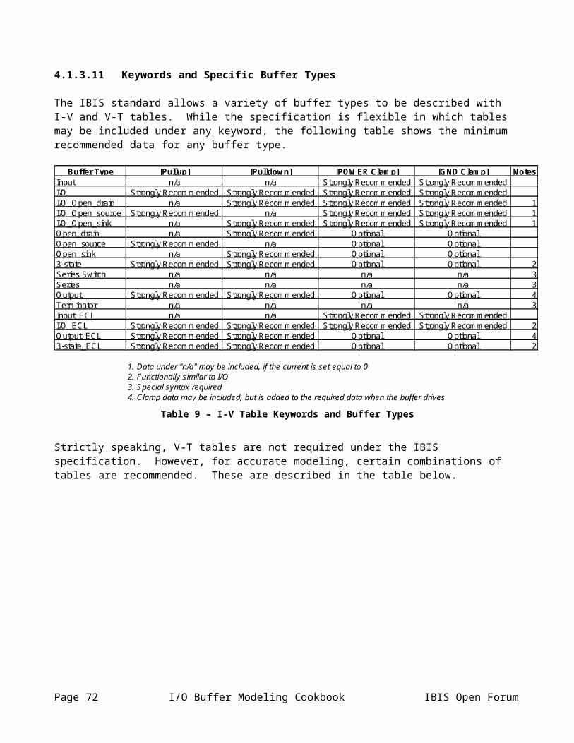
You can use any simulator that supports IBIS. Contact the simulator vendor and request their parser, converter, or application note on using IBIS models on their tools. To find simulator vendors that support IBIS, see the IBIS member organization list maintained on the IBIS web site.
6.0 Correlating the Data
The last step in the modeling process is to correlate the simulation results with actual silicon measurements. To obtain I-V tables and rise/fall time measurements, see the section titled Obtaining I-V and Switching Information via Lab Measurement.
Correlation involves measuring the I-V tables and rise/fall times of an actual IC and verifying that they fall within the maximum and minimum values used in the IBIS model. In addition, for ICs in a motherboard or other test setup driving a known load, compare the oscilloscope waveforms with simulation waveforms using the same load.
NoteThe oscilloscope adds a load to the circuit and the response of the oscilloscope affects the response measured.
A detailed set of recommendations for improving IBIS model accuracy can be found in the IBIS Accuracy Report, at http://www.eda.org/ibis/accuracy/, and in the IBIS Quality Checklist, http://www.sisoft.com/ibis-quality/.
IBIS Forum I/O Buffer Modeling Cookbook Page 73
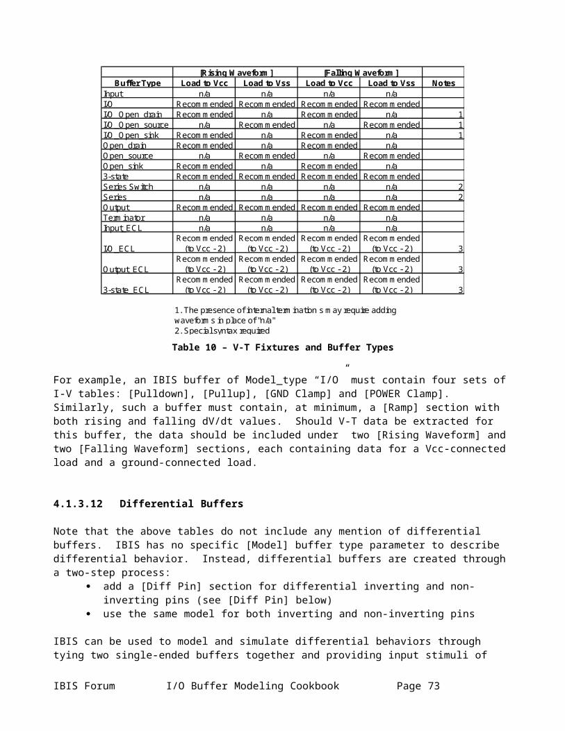
7.0 Resources
The IBIS Open Forum is a working group of the EIA and as such is responsible for the official IBIS specification. Minutes of IBIS meetings, email correspondence, proposals for specification changes, etc. are on-line at “eda.org”. To join in the email discussions, send a message to “[email protected]” and request that your name be added to the IBIS mail reflector. Be sure to include your email address.
To download a copy of the specification, the golden parser, various public-domain models, s2ibis and s2ibis3 programs and other information, visit the IBIS Web page.
WWW: http://www.eigroup.org/ibis/
Significant information is available through the IBIS Open Forum’s archive of IBIS Summit materials. Topics include IBIS performance at multi-gigahertz speeds, advanced modeling techniques and power delivery simulation using IBIS. The archive indicies are available at:
http://www.eda.org/ibis/summits/
Page 74 I/O Buffer Modeling Cookbook IBIS Open Forum


