
Impact of Manufacturing Defects on Carbon Nanotube Logic Circuits
D. Gil, D. de Andrés, J.-C. Ruiz, P. [email protected]
3rd Workshop on Dependable and Secure Nanocomputing
June 29 2009, Portugal

2
3rd Workshop on Dependable and Secure Nanocomputing, June 29 2009, Portugal
New technologies
Research
activity
Typical
examples
Device
122322449162379
Spin Gain transistor
Spin FET
Spin Torque transistor
Moving domain wall
M: QCA
Crossbar latch
Molecular transistor
Molecular QCA
SET
III-IV compound semiconductor and
Ge channel replacement
CNT FET
NW FET
NW hetero-structures
Nanorribontransistors with
graphene
Spin transistorFerromagnetic
logicMolecularSET
Channel
replacement
1D
structures
FET Extensions
3
3rd Workshop on Dependable and Secure Nanocomputing, June 29 2009, Portugal
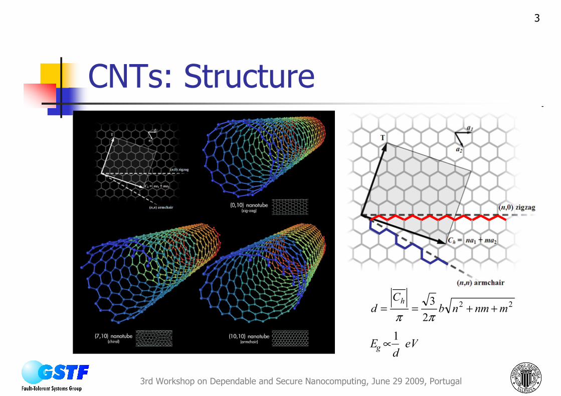
CNTs: Structure
22
2
3mnmnb
Cd
h++==
ππ
eVd
Eg 1
∝

4
3rd Workshop on Dependable and Secure Nanocomputing, June 29 2009, Portugal
CNTs: Properties & challenges
� Properties:
� Mechanical properties: strength, thermal conductivity
� Electrical: ballistic transport, excellent conduction properties
� Size: diameter ∼ few nm, length up to several mm
� Challenges of manufacturing at large scale
� Control of electrical properties (semic. /metallic)
� Alignment and placement
� Electrical contact between CNTs and electrodes
5
3rd Workshop on Dependable and Secure Nanocomputing, June 29 2009, Portugal
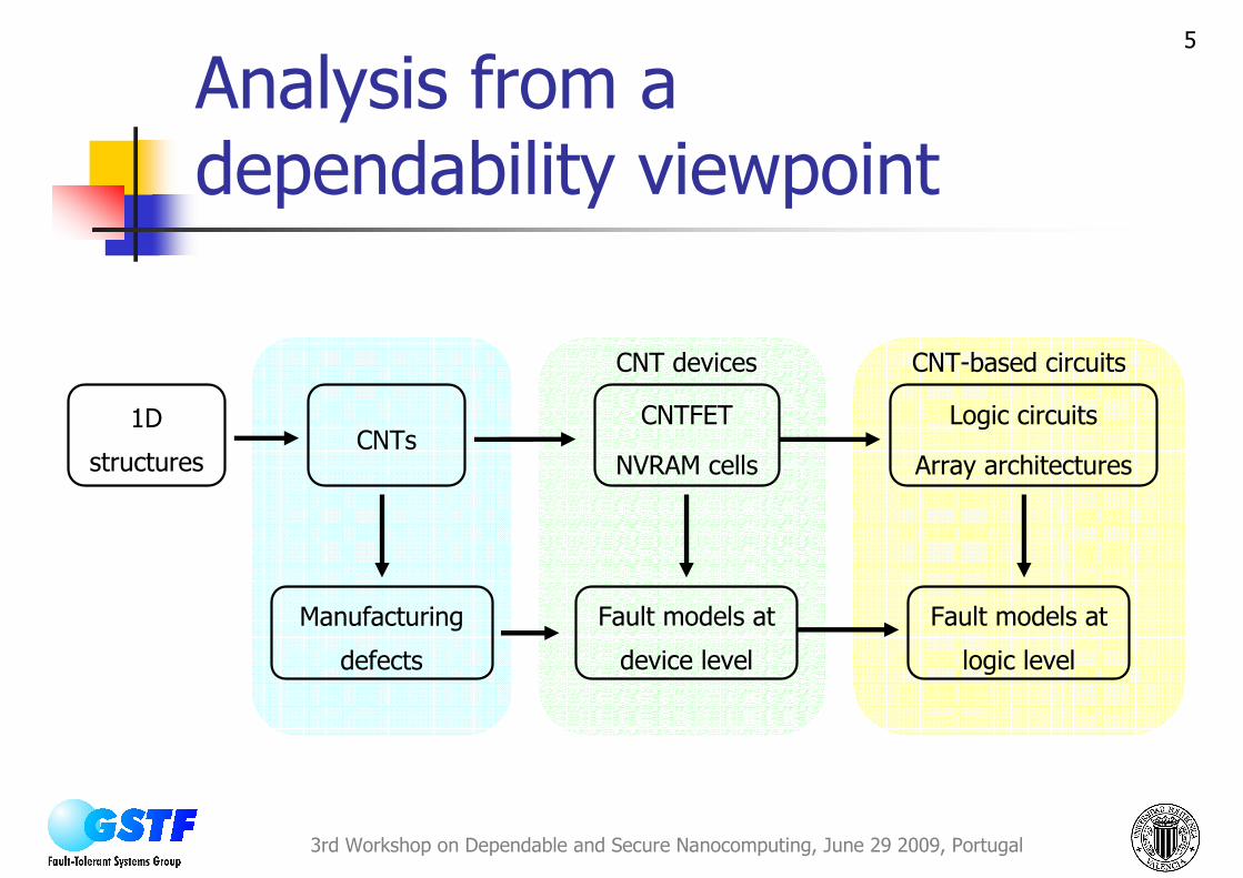
Analysis from a dependability viewpoint
1D
structuresCNTs
CNTFET
NVRAM cells
Logic circuits
Array architectures
Manufacturing
defects
Fault models at
device level
CNT devices CNT-based circuits
Fault models at
logic level
6
3rd Workshop on Dependable and Secure Nanocomputing, June 29 2009, Portugal
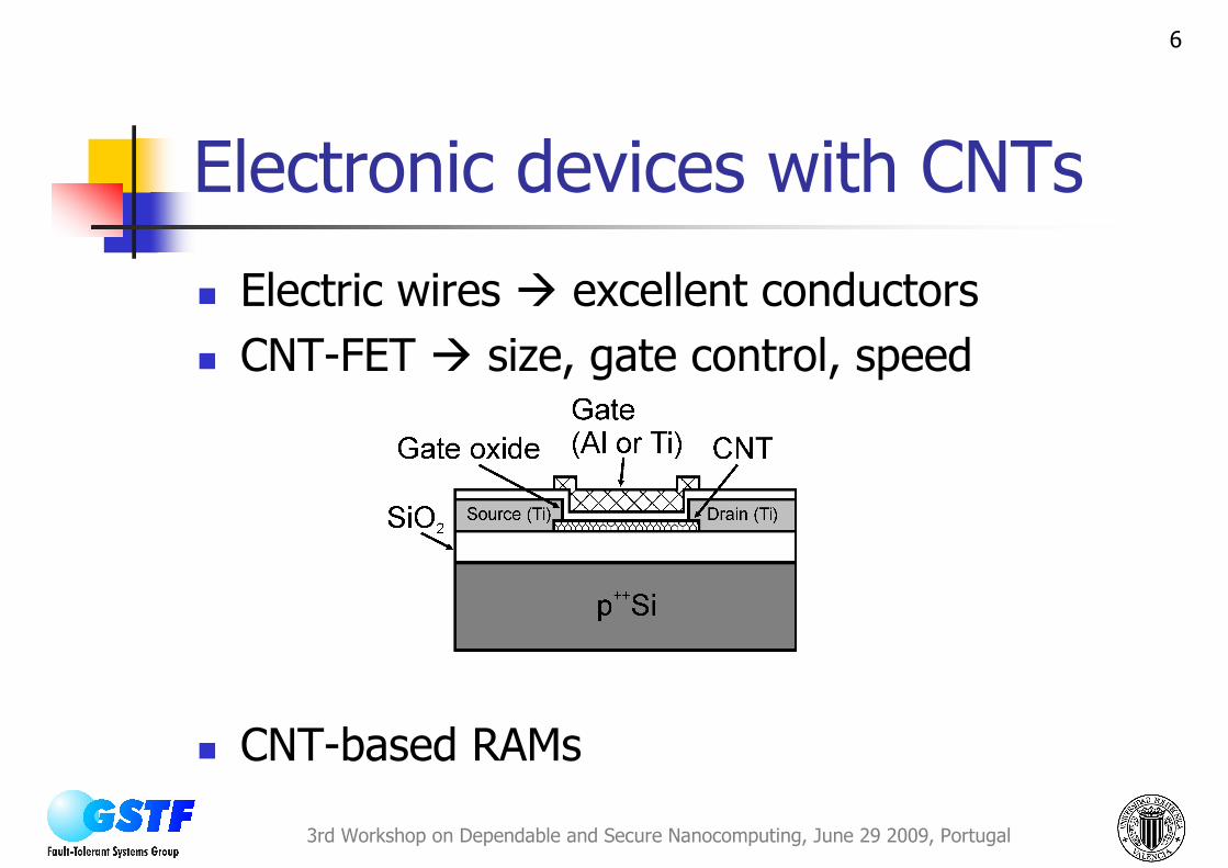
Electronic devices with CNTs
� Electric wires � excellent conductors
� CNT-FET � size, gate control, speed
� CNT-based RAMs
7
3rd Workshop on Dependable and Secure Nanocomputing, June 29 2009, Portugal
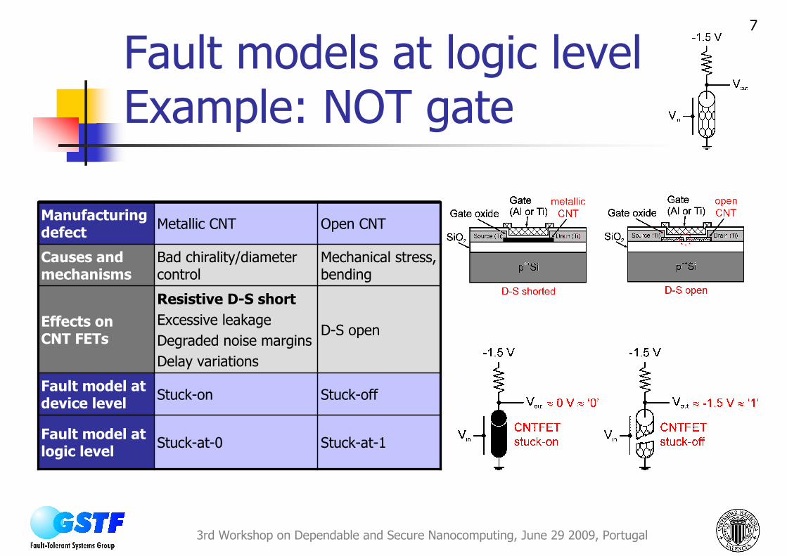
Fault models at logic level Example: NOT gate
Stuck-at-1
Stuck-off
D-S open
Mechanical stress, bending
Open CNT
Stuck-at-0
Stuck-on
Resistive D-S short
Excessive leakage
Degraded noise margins
Delay variations
Bad chirality/diameter control
Metallic CNT
Fault model at logic level
Fault model at device level
Manufacturing defect
Effects onCNT FETs
Causes and mechanisms

8
3rd Workshop on Dependable and Secure Nanocomputing, June 29 2009, Portugal
Fault models at logic level Example: NOT gate
Misaligned / Miss-positionedManufacturing defect
D-S open, connection with other transistors
D-S short
Effects onCNT FETs
CNT under incorrect gate
CNT outside gate
Causes and mechanisms
Stuck-onFault model at device level
Stuck-at-0Fault model at logic level
9
3rd Workshop on Dependable and Secure Nanocomputing, June 29 2009, Portugal
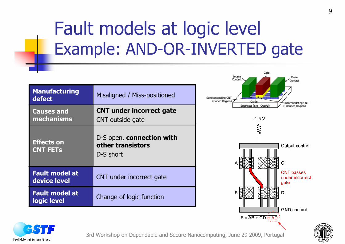
Fault models at logic level Example: AND-OR-INVERTED gate
Misaligned / Miss-positionedManufacturing defect
D-S open, connection with other transistors
D-S short
Effects onCNT FETs
CNT under incorrect gate
CNT outside gate
Causes and mechanisms
CNT under incorrect gateFault model at device level
Change of logic functionFault model at logic level

10
3rd Workshop on Dependable and Secure Nanocomputing, June 29 2009, Portugal
Fault models at logic level Example: Intramolecular NOT gate
Erroneous dopingManufacturing defect
Channel cannot be N-dopedEffects onCNT FETs
Misaligned PMMA maskCauses and mechanisms
2 P-CNTFETFault model at device level
Incorrect logic behaviourFault model at logic level
11
3rd Workshop on Dependable and Secure Nanocomputing, June 29 2009, Portugal
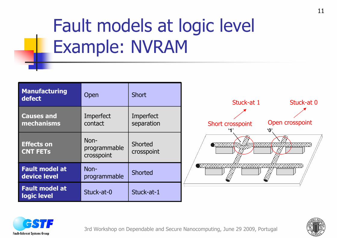
Fault models at logic level Example: NVRAM
Open crosspointShort crosspoint
Stuck-at 1 Stuck-at 0
Shorted crosspoint
Imperfect separation
ShortOpenManufacturing defect
Non-programmable crosspoint
Effects onCNT FETs
Imperfect contact
Causes and mechanisms
ShortedNon-programmable
Fault model at device level
Stuck-at-1Stuck-at-0Fault model at logic level
12
3rd Workshop on Dependable and Secure Nanocomputing, June 29 2009, Portugal
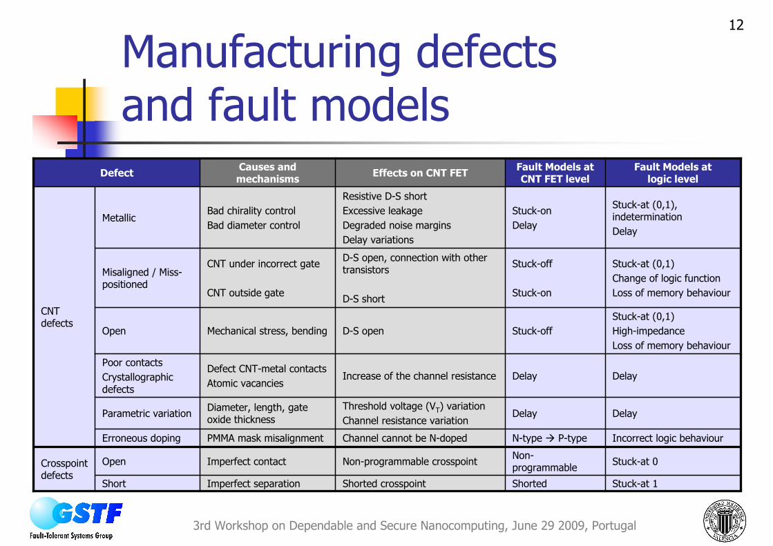
Manufacturing defectsand fault models
Stuck-at 1
Stuck-at 0
Incorrect logic behaviour
Delay
Delay
Stuck-at (0,1)
High-impedance
Loss of memory behaviour
Stuck-at (0,1)
Change of logic function
Loss of memory behaviour
Stuck-at (0,1), indetermination
Delay
Fault Models atlogic level
Shorted
Non-programmable
N-type � P-type
Delay
Delay
Stuck-off
Stuck-off
Stuck-on
Stuck-on
Delay
Fault Models atCNT FET level
Shorted crosspoint
Non-programmable crosspoint
Channel cannot be N-doped
Threshold voltage (VT) variation
Channel resistance variation
Increase of the channel resistance
D-S open
D-S open, connection with other transistors
D-S short
Resistive D-S short
Excessive leakage
Degraded noise margins
Delay variations
Effects on CNT FET
Imperfect contactOpen
Diameter, length, gate oxide thickness
Parametric variation
Defect CNT-metal contacts
Atomic vacancies
Poor contacts
Crystallographic defects
Mechanical stress, bendingOpen
Imperfect separationShort
Crosspointdefects
PMMA mask misalignmentErroneous doping
CNT under incorrect gate
CNT outside gate
Misaligned / Miss-positioned
Bad chirality control
Bad diameter controlMetallic
CNT defects
Causes and mechanisms
Defect

13
3rd Workshop on Dependable and Secure Nanocomputing, June 29 2009, Portugal
Conclusions
� Manufacturing defects
� Similar to SiNWs: Open, poor contacts, erroneous doping, and open/short crosspoints
� More specific, frequent and troublesome: Conducting (metallic), misaligned/miss-positioned, and
parametric variation of the CNTFET channel
� Fault models at transistor level
� Structural similarity to MOSFET transistors, Electronic charge-based devices � Well-known stuck-on,
stuck-off and delay
� Fault models at logic level
� CNT-based logic circuits present NMOS- or CMOS-like structures � Traditional stuck-at (0/1), delay,
high-impedance and indetermination:
� Some unusual fault models: Change of logic function, Inverter with 2 P-CNTFETs, Loss of memory
behaviour in SRAM cells

14
3rd Workshop on Dependable and Secure Nanocomputing, June 29 2009, Portugal
Any question?
Thank you forpaying attention!

Impact of Manufacturing Defects on Carbon Nanotube Logic Circuits
D. Gil, D. de Andrés, J.-C. Ruiz, P. [email protected]
Third Workshop on Dependable and Secure Nanocomputing
June 29 2009, Portugal


