

27 kW
10 kW
XRSPG
IN
VMON
10 Fm
10 Fm
10 Fm
SEQ
GND
VSET
5-V
Power
Supply
100 kW
100 kW
SS2SS1 CT2CT1
TEST
VDDIO-n
VD
D-n
VDDIO-3
VD
D-3
VDDIO-2
VD
D-2
VDDIO-1
VD
D-1
0.1 Fm
0.1 Fm
0.1 Fm0.1 Fm 0.1 Fm
0.1 Fm
0.1 Fm
0.1 Fm
C2000
Controller
TPS75005EN
GND
OUT2-S
OUT2
OUT1-S
OUT1
VDET
TPS75005
www.ti.com SBVS144C –NOVEMBER 2011–REVISED APRIL 2012
Integrated MCU Power Solution for C2000™ MicrocontrollersCheck for Samples: TPS75005
1FEATURES DESCRIPTIONThe TPS75005 is a complete power management
23• Optimized to Supply TI's C2000 MCU Series:solution for Texas Instruments' C2000 real-timeF2833x ( DELFINO™), F2823x, F281x, andmicrocontrollers and other DSP, FPGA, and ASICF280x/F2801xMCUs. The device has been tested with and meets
• Dual 500-mA Voltage Regulators with TI's F2833x (DELFINO), F2823x, F281x, andDedicated Supply Voltage Supervisors (SVSs) F280x/F2801x power requirements.
• One Auxiliary SVS All of these C2000 controllers require ±5% power-rail• LDO1 and SVS1 for 1.8 V/1.9 V (Selectable): accuracy. With the combination of high-accuracy,
±5% Specified with PG low-dropout regulators (LDOs) and dedicated SVSs,the device allows for a ±5% power supply to the• LDO2 and SVS2 for 3.3 V:C2000 with a power-good (PG) signal. (For more±5% Specified with PGdetails, see Application Report SBVA032, LDO+SVS
• Input Voltage Range: 3.75 V to 6.5 V Combined Accuracy.)• Independent Soft-Start for LDO1 and LDO2
Two power outputs are controlled by an integrated• Preset Power-Up and Power-Down Sequencing sequencer circuit. A single EN logic input signal
for C2000 MCUs makes sure that the power-up and power-downrequirements of the C2000 controllers are met. The• Supports C2000 MCU Transient with Twosequencer includes a soft-start for both LDOs to10-µF Ceramic Output Capacitorsavoid inrush current. A third rail monitor is provided
• 5-mm × 5-mm QFN Package (1)for general-purpose monitoring (for example, tomonitor input voltage).
APPLICATIONSA quick-start guide (SBVA030) is available with step-
• C2000 MCUs by-step instructions for connection to a C2000• DSPs/FPGAs/ASICs controller.
The TPS75005 is available in a 5-mm × 5-mm QFNpackage, yielding a compact total solution size with(1) 16-Pin HTSSOP package can be supported but minimum
quantity may be required; contact sales representative. high power dissipation capability.
1
Please be aware that an important notice concerning availability, standard warranty, and use in critical applications ofTexas Instruments semiconductor products and disclaimers thereto appears at the end of this data sheet.
2C2000, DELFINO are trademarks of Texas Instruments.3All other trademarks are the property of their respective owners.
PRODUCTION DATA information is current as of publication date. Copyright © 2011–2012, Texas Instruments IncorporatedProducts conform to specifications per the terms of the TexasInstruments standard warranty. Production processing does notnecessarily include testing of all parameters.

TPS75005
SBVS144C –NOVEMBER 2011–REVISED APRIL 2012 www.ti.com
This integrated circuit can be damaged by ESD. Texas Instruments recommends that all integrated circuits be handled withappropriate precautions. Failure to observe proper handling and installation procedures can cause damage.
ESD damage can range from subtle performance degradation to complete device failure. Precision integrated circuits may be moresusceptible to damage because very small parametric changes could cause the device not to meet its published specifications.
VOLTAGE INFORMATION (1)
PRODUCT VOUT1 VOUT2 VSVS1 VSVS2 VSVS3
VSET = L VSET = H VSET = H VSET = L3.333 V 3.234TPS75005 (2)
1.818 V 1.919 V 1.764 V 1.862 V(101%) (98%)(101%) (101%) (98%) (98%) 1.206 V
Adjustable, Adjustable, Adjustable, Adjustable,TPS75005ADJ greater than 1.24 V greater than 1.24 V 97% of VOUT1 97% of VOUT2
(1) For the most current package and ordering information see the Package Option Addendum at the end of this document, or visit thedevice product folder at www.ti.com.
(2) VOUT1 and VSVS1 are selectable by VSET pin logic with the TPS75005.
ABSOLUTE MAXIMUM RATINGS (1)
At TJ = –40°C to +125°C (unless otherwise noted).
VALUE UNIT
MIN MAX
IN, OUT1, OUT2, VMON, VSET, SEQ, OUT1_S, OUT2_S –0.3 +7.0 V
Voltage (2) CT1 CT2, SS1, SS2 –0.3 +3.6 V
EN, VDET, PG, TEST –0.3 VIN + 0.3 (3) V
Output current Internally limited (4)
Temperature Storage, Tstg –55 +150 °C
Human body model (HBM) QSS 009-105 (JESD22-A114A) 2 kVElectrostaticdischarge ratings (5)
Charge device model (CDM) QSS 009-147 (JESD22-C101B.01) 500 V
(1) Stresses beyond those listed under Absolute Maximum Ratings may cause permanent damage to the device. These are stress ratingsonly, and functional operation of the device at these or any other conditions beyond those indicated is not implied. Exposure to absolute-maximum-rated conditions for extended periods my affect device reliability.
(2) All voltages are with respect to network ground terminal.(3) Absolute maximum rating of these pins is VIN + 0.3 V or + 7.0 V, whichever is smaller.(4) See Electrical Characteristics.(5) ESD testing is performed according to the respective JESD22 JEDEC standard.
2 Submit Documentation Feedback Copyright © 2011–2012, Texas Instruments Incorporated
Product Folder Link(s): TPS75005

TPS75005
www.ti.com SBVS144C –NOVEMBER 2011–REVISED APRIL 2012
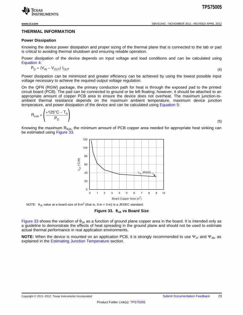
THERMAL INFORMATIONTPS75005
THERMAL METRIC (1) (2) RGW (QFN) (3) UNITS
20 PINS
θJA Junction-to-ambient thermal resistance (4) 35.1
θJCtop Junction-to-case (top) thermal resistance (5) 31.9
θJB Junction-to-board thermal resistance (6) 14.4°C/W
ψJT Junction-to-top characterization parameter (7) 0.4
ψJB Junction-to-board characterization parameter (8) 14.5
θJCbot Junction-to-case (bottom) thermal resistance (9) 3.7
(1) For more information about traditional and new thermal metrics, see the IC Package Thermal Metrics application report, SPRA953A.(2) For thermal estimates of this device based on PCB copper area, see the TI PCB Thermal Calculator.(3) Thermal data for the RGW package is derived by thermal simulations based on JEDEC-standard methodology as specified in the
JESD51 series. The following assumptions are used in the simulations:(a) RGW: The exposed pad is connected to the PCB ground layer through a 4 x 4 thermal via array.(b) Each of top and bottom copper layers has a dedicated pattern for 4% copper coverage.(c) These data were generated with only a single device at the center of a JEDEC high-K (2s2p) board with 3in × 3in copper area. To
understand the effects of the copper area on thermal performance, refer to the Power Dissipation and Estimating JunctionTemperature sections.
(4) The junction-to-ambient thermal resistance under natural convection is obtained in a simulation on a JEDEC-standard, high-K board, asspecified in JESD51-7, in an environment described in JESD51-2a.
(5) The junction-to-case (top) thermal resistance is obtained by simulating a cold plate test on the top of the package. No specific JEDEC-standard test exists, but a close description can be found in the ANSI SEMI standard G30-88.
(6) The junction-to-board thermal resistance is obtained by simulating in an environment with a ring cold plate fixture to control the PCBtemperature, as described in JESD51-8.
(7) The junction-to-top characterization parameter, ψJT, estimates the junction temperature of a device in a real system and is extractedfrom the simulation data to obtain θJA using a procedure described in JESD51-2a (sections 6 and 7).
(8) The junction-to-board characterization parameter, ψJB, estimates the junction temperature of a device in a real system and is extractedfrom the simulation data to obtain θJA using a procedure described in JESD51-2a (sections 6 and 7).
(9) The junction-to-case (bottom) thermal resistance is obtained by simulating a cold plate test on the exposed (power) pad. No specificJEDEC standard test exists, but a close description can be found in the ANSI SEMI standard G30-88.
Copyright © 2011–2012, Texas Instruments Incorporated Submit Documentation Feedback 3
Product Folder Link(s): TPS75005

TPS75005
SBVS144C –NOVEMBER 2011–REVISED APRIL 2012 www.ti.com
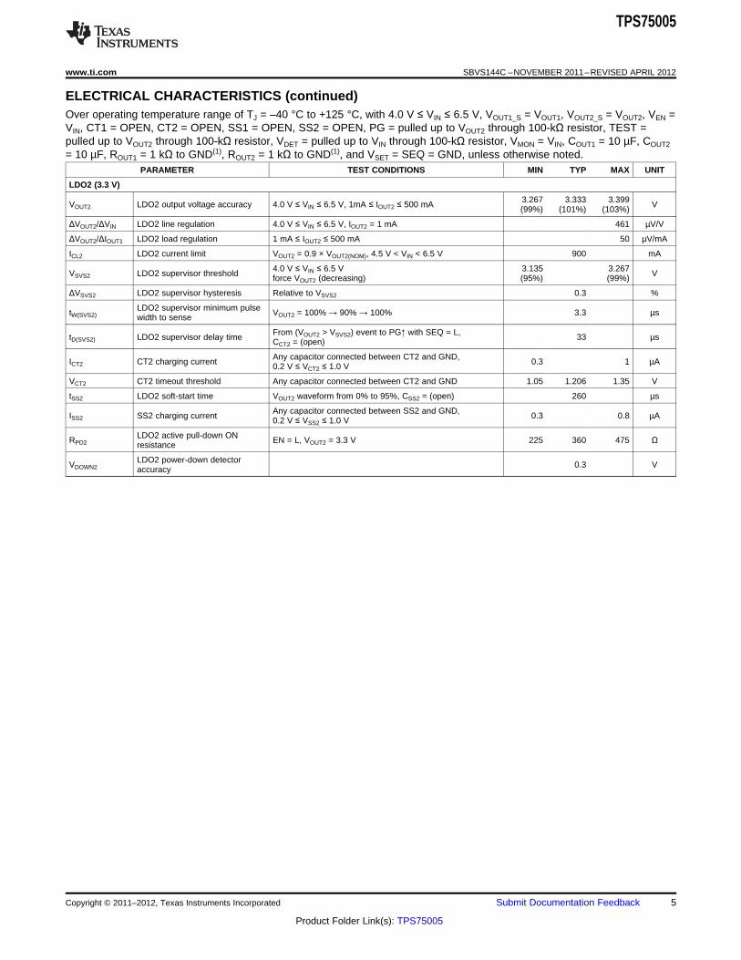
ELECTRICAL CHARACTERISTICSOver operating temperature range of TJ = –40 °C to +125 °C, with 4.0 V ≤ VIN ≤ 6.5 V, VOUT1_S = VOUT1, VOUT2_S = VOUT2, VEN =VIN, CT1 = OPEN, CT2 = OPEN, SS1 = OPEN, SS2 = OPEN, PG = pulled up to VOUT2 through 100-kΩ resistor, TEST =pulled up to VOUT2 through 100-kΩ resistor, VDET = pulled up to VIN through 100-kΩ resistor, VMON = VIN, COUT1 = 10 µF, COUT2
= 10 µF, ROUT1 = 1 kΩ to GND (1), ROUT2 = 1 kΩ to GND (1), and VSET = SEQ = GND, unless otherwise noted.PARAMETER TEST CONDITIONS MIN TYP MAX UNIT
COMPLETE DEVICE
VIN Input voltage range 3.75 6.5 V
IGND GND current IOUT1 = IOUT2 = 500 mA, VSET = VIN or GND 500 µA
IQ Quiescent GND current IOUT1 = IOUT2 = 0 A, VSET = VIN or GND 175 µA
ISHDN Shutdown ground current VIN = 6.5 V, no pull-up resistors at PG, VDET, TEST pins 17 40 µA
VSVS3 VMON supervisor threshold 1.181 1.206 1.230 V
ΔVSVS3 VMON supervisor hysteresis Relative to VSVS3 + 4 mV
VIH High-level input voltage For EN, SEQ, and VSET pins 2.0 V
VIL Low-level input voltage For EN, SEQ, and VSET pins 0 0.8 V
For SEQ and VSET pins, VSEQ = VSET = 2.0 V – 0.1 0.1IIN Logic input current µA
For EN pin – 0.2 0.2
Load current 1 mA into PG, TEST, and VDET pinsVOL Low-level output voltage 0.3 Vforce VOUT1 < VSVS1, VMON = 0.5 V
Releasing: VIN rising 3.4 3.75 VUVLO Undervoltage lock out
Locking: hysteresis, VIN falling 60 mV
Temperature rising to shutdown +165 °CTTSD Thermal shutdown temperature
Hysteresis, temperature falling to release shutdown +145 °C
tDVS VSET transition time (2) 40 µs
LDO1 (1.8 V or 1.9 V Selectable by VSET Pin)
1.881 1.919 1.957VSET= H, 4.0 V ≤ VIN ≤ 6.5 V, 1 mA ≤ IOUT1 ≤ 500 mA V(99%) (101%) (103%)VOUT1 LDO1 output voltage accuracy
1.782 1.818 1.854VSET= L, 4.0 V ≤ VIN ≤ 6.5 V, 1 mA ≤ IOUT1 ≤ 500 mA V(99%) (101%) (103%)
ΔVOUT1/ΔVIN LDO1 line regulation 4.0 V ≤ VIN ≤ 6.5 V, IOUT1 = 1 mA 122 µV/V
ΔVOUT1/ΔIOUT1 LDO1 load regulation 1 mA ≤ IOUT1 ≤ 500 mA 29 µV/mA
ICL1 LDO1 current limit VOUT1 = 0.9 × VOUT1(NOM), 4.5 V < VIN < 6.5 V 900 mA
VSET= H, 4.0 V ≤ VIN ≤ 6.5 V 1.805 1.881 VForce VOUT1 (decreasing) (95%) (99%)VSVS1 LDO1 supervisor threshold
VSET= L, 4.0 V ≤ VIN ≤ 6.5 V 1.710 1.782 VForce VOUT1 (decreasing) (95%) (99%)
ΔVSVS1 LDO1 supervisor hysteresis Relative to VSVS1 0.3 %
LDO1 supervisor minimum pulsetW(SVS1) VOUT1 = 100% → 90% → 100% 3.3 µswidth to Sense
From (VOUT1 > VSVS1) event to PG ↑ with SEQ = H,tD(SVS1) LDO1 supervisor delay time 33 µsCCT1 = (open)
Any capacitor connected between CT1 and GND,ICT1 CT1 charging current 0.3 1 µA0.2 V ≤ VCT1 ≤ 1.0 V
VCT1 CT1 timeout threshold Any capacitor connected between CT1 and GND 1.05 1.206 1.35 V
tSS1 LDO1 soft-start time VOUT1 waveform from 0% to 95%, CSS1 = (open) 260 µs
Any capacitor connected between SS1 and GND,ISS1 SS1 charging current 0.3 0.8 µA0.2 V ≤ VSS1 ≤ 1.0 V
LDO1 active pull-down ONRPD1 EN = GND, VOUT1 = 1.8 V 225 360 475 Ωresistance
LDO1 power-down detectorVDOWN1 0.3 Vaccuracy
(1) These 1-kΩ resistors are disconnected when the test conditions specify an output current of LDO1 or LDO2.(2) With recommended usage of TPS75005, VSET does not need to be controlled on-the-fly. VSET transition time varies significantly
depending on application conditions. Stated typical value is almost the fastest transition.
4 Submit Documentation Feedback Copyright © 2011–2012, Texas Instruments Incorporated
Product Folder Link(s): TPS75005
TPS75005
www.ti.com SBVS144C –NOVEMBER 2011–REVISED APRIL 2012
ELECTRICAL CHARACTERISTICS (continued)Over operating temperature range of TJ = –40 °C to +125 °C, with 4.0 V ≤ VIN ≤ 6.5 V, VOUT1_S = VOUT1, VOUT2_S = VOUT2, VEN =VIN, CT1 = OPEN, CT2 = OPEN, SS1 = OPEN, SS2 = OPEN, PG = pulled up to VOUT2 through 100-kΩ resistor, TEST =pulled up to VOUT2 through 100-kΩ resistor, VDET = pulled up to VIN through 100-kΩ resistor, VMON = VIN, COUT1 = 10 µF, COUT2
= 10 µF, ROUT1 = 1 kΩ to GND(1), ROUT2 = 1 kΩ to GND(1), and VSET = SEQ = GND, unless otherwise noted.PARAMETER TEST CONDITIONS MIN TYP MAX UNIT
LDO2 (3.3 V)
3.267 3.333 3.399VOUT2 LDO2 output voltage accuracy 4.0 V ≤ VIN ≤ 6.5 V, 1mA ≤ IOUT2 ≤ 500 mA V(99%) (101%) (103%)
ΔVOUT2/ΔVIN LDO2 line regulation 4.0 V ≤ VIN ≤ 6.5 V, IOUT2 = 1 mA 461 µV/V
ΔVOUT2/ΔIOUT1 LDO2 load regulation 1 mA ≤ IOUT2 ≤ 500 mA 50 µV/mA
ICL2 LDO2 current limit VOUT2 = 0.9 × VOUT2(NOM), 4.5 V < VIN < 6.5 V 900 mA
4.0 V ≤ VIN ≤ 6.5 V 3.135 3.267VSVS2 LDO2 supervisor threshold Vforce VOUT2 (decreasing) (95%) (99%)
ΔVSVS2 LDO2 supervisor hysteresis Relative to VSVS2 0.3 %
LDO2 supervisor minimum pulsetW(SVS2) VOUT2 = 100% → 90% → 100% 3.3 µswidth to sense
From (VOUT2 > VSVS2) event to PG↑ with SEQ = L,tD(SVS2) LDO2 supervisor delay time 33 µsCCT2 = (open)
Any capacitor connected between CT2 and GND,ICT2 CT2 charging current 0.3 1 µA0.2 V ≤ VCT2 ≤ 1.0 V
VCT2 CT2 timeout threshold Any capacitor connected between CT2 and GND 1.05 1.206 1.35 V
tSS2 LDO2 soft-start time VOUT2 waveform from 0% to 95%, CSS2 = (open) 260 µs
Any capacitor connected between SS2 and GND,ISS2 SS2 charging current 0.3 0.8 µA0.2 V ≤ VSS2 ≤ 1.0 V
LDO2 active pull-down ONRPD2 EN = L, VOUT2 = 3.3 V 225 360 475 Ωresistance
LDO2 power-down detectorVDOWN2 0.3 Vaccuracy
Copyright © 2011–2012, Texas Instruments Incorporated Submit Documentation Feedback 5
Product Folder Link(s): TPS75005
NC
IN IN EN
VM
ON
1
2
3
4
5
620
719
818
917
10
16
15
14
13
12
11
OUT2 OUT1
OUT1_S
CT1
SS1
TEST
GN
D
GN
D
SE
Q
VS
ET
PG
OUT2_S
CT2
SS2
VDET
TPS75005
SBVS144C –NOVEMBER 2011–REVISED APRIL 2012 www.ti.com
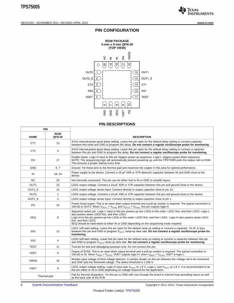
PIN CONFIGURATION
RGW PACKAGE5-mm x 5-mm QFN-20
(TOP VIEW)
PIN DESCRIPTIONSPIN
RGWNAME QFN-20 DESCRIPTION
SVS1 internal-power-good delay setting. Leave this pin open for the default delay setting or connect capacitorCT1 13 between this node and GND to program the delay. Do not connect a regular oscilloscope probe for monitoring.
SVS2 internal-power-good delay setting. Leave this pin open for the default delay setting or connect a capacitorCT2 3 between this pin and GND to program the delay. Do not connect a regular oscilloscope probe for monitoring.
Enable inputs. Logic-H input to this pin triggers power-up sequence. Logic-L triggers power-down sequence.EN 17 NOTE: The sequencing logic will automatically prevent powering up until the TPS75005 pulls the output rails to GND.
This ensures a proper startup every time.
GND 6, 7 Ground. Tie these pins to the thermal pad and maximize the copper in this area for optimal performance.
Power supply to the device. Connect a 10-µF X5R or X7R dielectric capacitor between IN and GND close to theIN 18, 19 device.
NC 20 Not internally connected. This pin can be either tied to IN or GND to simplify layout.
OUT1 15 LDO1 output voltage. Connect a 10-µF X5R or X7R capacitor between this pin and ground close to the device.
OUT1_S 14 LDO1 output voltage sense input. Connect directly to output capacitor close to pin 15.
OUT2 1 LDO2 output voltage. Connect a 10-µF X5R or X7R capacitor between this pin and ground close to the device.
OUT2_S 2 LDO2 output voltage sense input. Connect directly to output capacitor close to pin 1.
Power-Good output. This is an open-drain output terminal and a pull-up resistor is required. The typical connection isPG 10 100 kΩ to OUT2. When VOUT1 > VSVS1 and VOUT2 > VSVS2, this pin outputs logic-H.
Sequence select pin. Logic-L input to this pin powers-up two LDOs in this order: LDO1 first, and then LDO2. Logic-Lalso powers-down LDO2 first, and then LDO1.
SEQ 8 Logic-H to this pin powers-up two LDOs in this order: LDO2 first, and then LDO1. Logic-H also powers-down LDO1first, and then LDO2.SEQ should be hard-wired to either IN or GND depending on the sequencing mode required.
LDO1 soft-start setting. Leave this pin open for the default ramp up setting or connect a capacitor, 10 nF or less,SS1 12 between this pin and GND to program VOUT1 ramp-up slew rate. Do not connect a regular oscilloscope probe for
monitoring.
LDO2 soft-start setting. Leave this pin open for the default ramp up setting or connect a capacitor between this pinSS2 4 and GND to program VOUT2 ramp-up slew rate. Do not connect a regular oscilloscope probe for monitoring.
TEST 11 Test pin for test and debugging purposes only. Do not connect this pin.
Output of SVS3. This is an open-drain output terminal and a pull-up resistor is required. The typical connection isVDET 5 100 kΩ to IN. When VMON > VSVS3, VDET outputs logic-H; when VMON < VSVS3, VDET is logic-L.
Monitor input voltage of third voltage detector. A resistor divider on this pin between the voltage rail to be monitoredVMON 16 and GND sets the threshold voltage. The detect threshold is 1.206 V.
LDO1 output voltage setting. Logic-H input sets VOUT1 to 1.9 V. Logic-L sets VOUT1 to 1.8 V. It is recommended to tieVSET 9 this pin either to IN or GND depending on voltage required for the application.
Pad for thermal dissipation. Tie this pin to GND with vias through the board to internal heat spreading layers as wellThermal pad as the back side of the PCB.
6 Submit Documentation Feedback Copyright © 2011–2012, Texas Instruments Incorporated
Product Folder Link(s): TPS75005

UVLO
TSD
UVLO97%
TSD
BG
EN1
EN2
CL1
EN1
EN2
CL1
PD1
CL1
0.3 V
PG1
SW1
SW2
VS1
Delay
PD2
0.3 V
PG2Delay
A
A
I > I ?OUT1 CL1
CL2I > I ?OUT2 CL2
CT1CT2SS2 SS1GND
PD1
EN1
CL1
PG1
PD2
EN2
CL2
PG2
UVLO
TSD
SW1
SW2
ControlLogic
Sequencer
EN
SEQ
VMON
IN
VSET
VS1
PG
TEST
VDET
OUT1
OUT2
OUT1_S
OUT2_S
V
1.8 V/500 mACORE
V
3.3 V/500 mAIO
110 pF
110 pF
2 pF2 pF
360 W
360 W
(Optional)
0.3 V
97%
97%
TPS75005
www.ti.com SBVS144C –NOVEMBER 2011–REVISED APRIL 2012
FUNCTIONAL BLOCK DIAGRAM
Figure 1. Functional Block Diagram
Copyright © 2011–2012, Texas Instruments Incorporated Submit Documentation Feedback 7
Product Folder Link(s): TPS75005
1.710
1.728
1.746
1.764
1.782
1.800
1.818
1.836
1.854
1.872
1.890
−50 −25 0 25 50 75 100 125Temperature (°C)
Vol
tage
(V
)
VSVS1 at VIN = 4.0 VVSVS1 at VIN = 5.0 VVSVS1 at VIN = 6.5 V
VOUT1 at VIN = 4.0 VVOUT1 at VIN = 5.0 VVOUT1 at VIN = 6.5 V
Y axis is 1%/div scale by referring 1.8 V.LDO1 is loaded at 250 mA.
G000
3.135
3.168
3.201
3.234
3.267
3.300
3.333
3.366
3.399
3.432
3.465
−50 −25 0 25 50 75 100 125Temperature (°C)
Vol
tage
(V
)
VSVS2 at VIN = 4.0 VVSVS2 at VIN = 5.0 VVSVS2 at VIN = 6.5 V
VOUT2 at VIN = 4.0 VVOUT2 at VIN = 5.0 VVOUT2 at VIN = 6.5 V
Y axis is 1%/div scale by referring 3.3 V.LDO2 is loaded at 250 mA.
G001
1.710
1.728
1.746
1.764
1.782
1.800
1.818
1.836
1.854
1.872
1.890
0 0.1 0.1 0.2 0.2 0.2 0.3 0.4 0.4 0.5 0.5OUT1 Output Current (A)
Vol
tage
(V
)
−40°C25°C85°C125°C
Y axis is 1%/div scale by referring 1.8 V.LDO1 is loaded at 25 mA.
G002
3.135
3.168
3.201
3.234
3.267
3.300
3.333
3.366
3.399
3.432
3.465
0 0.1 0.1 0.2 0.2 0.2 0.3 0.4 0.4 0.5 0.5OUT2 Output Current (A)
Vol
tage
(V
)
−40°C25°C85°C125°C
Y axis is 1%/div scale by referring 3.3 V.LDO2 is loaded at 25 mA.
G003
0
10
20
30
40
50
−50 −25 0 25 50 75 100 125Temperature (°C)
Shu
tdow
n G
roun
d C
urre
nt (
µA)
VIN = 4.0 VVIN = 5.0 VVIN = 6.5 V
The device is disabled. The graphshows consumption current byinternal reference circuits for SVS3.
G004
0
50
100
150
200
250
300
350
−50 −25 0 25 50 75 100 125Temperature (°C)
Qui
esce
nt G
roun
d C
urre
nt (
µA)
VIN = 4.0 VVIN = 5.0 VVIN = 6.5 V
PG, VDET, and TEST are open.LDO1 and LDO2 are enabledbut not loaded.
G005
TPS75005
SBVS144C –NOVEMBER 2011–REVISED APRIL 2012 www.ti.com
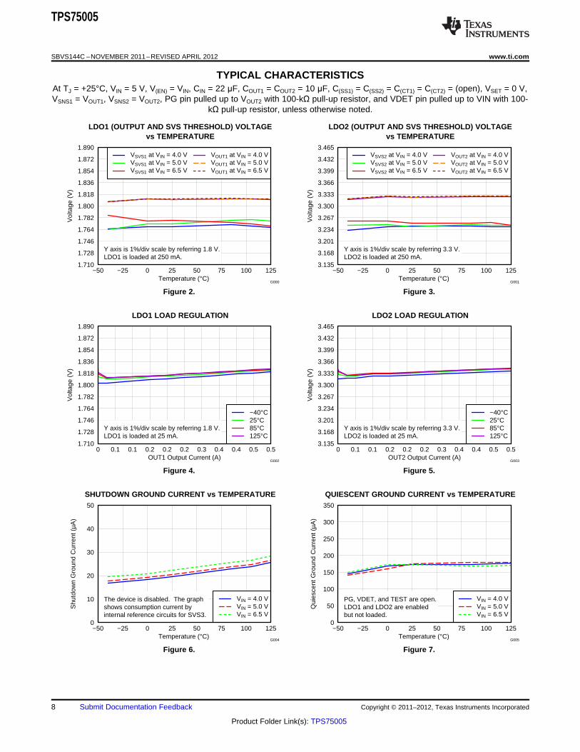
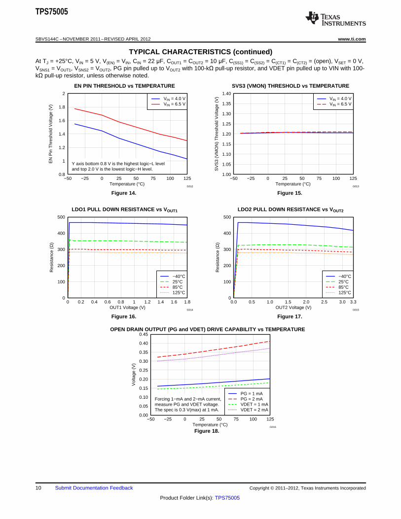
TYPICAL CHARACTERISTICSAt TJ = +25°C, VIN = 5 V, V(EN) = VIN, CIN = 22 μF, COUT1 = COUT2 = 10 μF, C(SS1) = C(SS2) = C(CT1) = C(CT2) = (open), VSET = 0 V,VSNS1 = VOUT1, VSNS2 = VOUT2, PG pin pulled up to VOUT2 with 100-kΩ pull-up resistor, and VDET pin pulled up to VIN with 100-
kΩ pull-up resistor, unless otherwise noted.
LDO1 (OUTPUT AND SVS THRESHOLD) VOLTAGE LDO2 (OUTPUT AND SVS THRESHOLD) VOLTAGEvs TEMPERATURE vs TEMPERATURE
Figure 2. Figure 3.
LDO1 LOAD REGULATION LDO2 LOAD REGULATION
Figure 4. Figure 5.
SHUTDOWN GROUND CURRENT vs TEMPERATURE QUIESCENT GROUND CURRENT vs TEMPERATURE
Figure 6. Figure 7.
8 Submit Documentation Feedback Copyright © 2011–2012, Texas Instruments Incorporated
Product Folder Link(s): TPS75005
0
50
100
150
200
250
300
350
0 0.1 0.2 0.3 0.4 0.5OUT1 Output Current (A)
Load
ed G
roun
d C
urre
nt (
µA)
−40°C25°C85°C125°C
PG, VDET, and TEST are open.LDO2 is loaded with 250 mA.
G007
0
50
100
150
200
250
300
350
0 0.1 0.2 0.3 0.4 0.5OUT2 Output Current (A)
Load
ed G
roun
d C
urre
nt (
µA)
−40°C25°C85°C125°C
PG, VDET, and TEST are open.LDO1 is loaded with 250 mA.
G008
0
50
100
150
200
250
300
350
−50 −25 0 25 50 75 100 125Temperature (°C)
Load
ed G
roun
d C
urre
nt (
µA)
VIN = 4.0 VVIN = 5.0 VVIN = 6.5 V
PG, VDET, and TEST are open.LDO1 and LDO2 are loadedwith 250 mA each.
G006
3.40
3.45
3.50
3.55
3.60
3.65
3.70
−50 −25 0 25 50 75 100 125Temperature (°C)
Inpu
t Vol
tage
(V
)UVLO (VIN goes up, device starts working)UVLO (VIN goes down, device locks)
G009
0
0.2
0.4
0.6
0.8
1
1.2
−50 −25 0 25 50 75 100 125Temperature (°C)
OU
T1
Cur
rent
Lim
it (A
)
VIN = 4.0 VVIN = 5.0 VVIN = 6.5 V
Under high temperature conditions,some units start hitting thermalshutdown during this test.
G010
0
0.2
0.4
0.6
0.8
1
1.2
−50 −25 0 25 50 75 100 125Temperature (°C)
OU
T2
Cur
rent
Lim
it (A
)
VIN = 4.0 VVIN = 5.0 VVIN = 6.5 V
G011
TPS75005
www.ti.com SBVS144C –NOVEMBER 2011–REVISED APRIL 2012
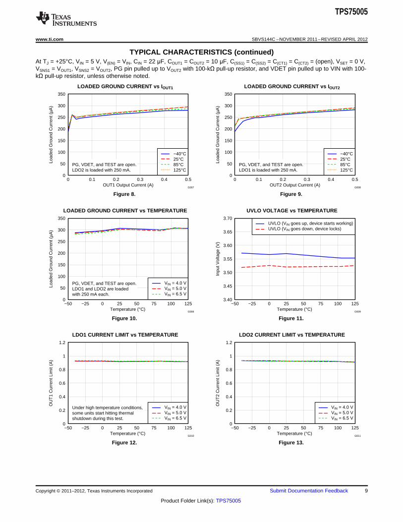
TYPICAL CHARACTERISTICS (continued)At TJ = +25°C, VIN = 5 V, V(EN) = VIN, CIN = 22 μF, COUT1 = COUT2 = 10 μF, C(SS1) = C(SS2) = C(CT1) = C(CT2) = (open), VSET = 0 V,VSNS1 = VOUT1, VSNS2 = VOUT2, PG pin pulled up to VOUT2 with 100-kΩ pull-up resistor, and VDET pin pulled up to VIN with 100-kΩ pull-up resistor, unless otherwise noted.
LOADED GROUND CURRENT vs IOUT1 LOADED GROUND CURRENT vs IOUT2
Figure 8. Figure 9.
LOADED GROUND CURRENT vs TEMPERATURE UVLO VOLTAGE vs TEMPERATURE
Figure 10. Figure 11.
LDO1 CURRENT LIMIT vs TEMPERATURE LDO2 CURRENT LIMIT vs TEMPERATURE
Figure 12. Figure 13.
Copyright © 2011–2012, Texas Instruments Incorporated Submit Documentation Feedback 9
Product Folder Link(s): TPS75005
0.8
1
1.2
1.4
1.6
1.8
2
−50 −25 0 25 50 75 100 125Temperature (°C)
EN
Pin
Thr
esho
ld V
olta
ge (
V)
VIN = 4.0 VVIN = 6.5 V
Y axis bottom 0.8 V is the highest logic−L leveland top 2.0 V is the lowest logic−H level.
G012
1.00
1.05
1.10
1.15
1.20
1.25
1.30
1.35
1.40
−50 −25 0 25 50 75 100 125Temperature (°C)
SV
S3
(VM
ON
) T
hres
hold
Vol
tage
(V
) VIN = 4.0 VVIN = 6.5 V
G013
0
100
200
300
400
500
0 0.2 0.4 0.6 0.8 1 1.2 1.4 1.6 1.8OUT1 Voltage (V)
Res
ista
nce
(Ω)
−40°C25°C85°C125°C
G014
0
100
200
300
400
500
0.0 0.5 1.0 1.5 2.0 2.5 3.0 3.3OUT2 Voltage (V)
Res
ista
nce
(Ω)
−40°C25°C85°C125°C
G015
0.00
0.05
0.10
0.15
0.20
0.25
0.30
0.35
0.40
0.45
−50 −25 0 25 50 75 100 125Temperature (°C)
Vol
tage
(V
)
PG = 1 mAPG = 2 mAVDET = 1 mAVDET = 2 mA
Forcing 1−mA and 2−mA current,measure PG and VDET voltage.The spec is 0.3 V(max) at 1 mA.
G016
TPS75005
SBVS144C –NOVEMBER 2011–REVISED APRIL 2012 www.ti.com
TYPICAL CHARACTERISTICS (continued)At TJ = +25°C, VIN = 5 V, V(EN) = VIN, CIN = 22 μF, COUT1 = COUT2 = 10 μF, C(SS1) = C(SS2) = C(CT1) = C(CT2) = (open), VSET = 0 V,VSNS1 = VOUT1, VSNS2 = VOUT2, PG pin pulled up to VOUT2 with 100-kΩ pull-up resistor, and VDET pin pulled up to VIN with 100-kΩ pull-up resistor, unless otherwise noted.
EN PIN THRESHOLD vs TEMPERATURE SVS3 (VMON) THRESHOLD vs TEMPERATURE
Figure 14. Figure 15.
LDO1 PULL DOWN RESISTANCE vs VOUT1 LDO2 PULL DOWN RESISTANCE vs VOUT2
Figure 16. Figure 17.
OPEN DRAIN OUTPUT (PG and VDET) DRIVE CAPABILITY vs TEMPERATURE
Figure 18.
10 Submit Documentation Feedback Copyright © 2011–2012, Texas Instruments Incorporated
Product Folder Link(s): TPS75005
1
2
3
4
5
6
VIN
1.78
1.8
1.82
1.84
1.86
1.88
Time (10 µs/div)
VIN
Vol
tage
(V
)
VO
UT
1 V
olta
ge (
V)
VOUT1
LDO1 is loaded at 250 mA.
G017
1
2
3
4
5
6
VIN
3.32
3.34
3.36
3.38
3.4
3.42
Time (10 µs/div)
VIN
Vol
tage
(V
)
VO
UT
2 V
olta
ge (
V)
VOUT2
LDO2 is loaded at 250 mA.
G023
0
1
2
3
4
5
VIN
IOUT1 (20 mA to 500 mA)
1.71
1.728
1.746
1.764
1.782
1.8
1.818
1.836
1.854
1.872
1.89
Time (10 µs/div)
VIN
Vol
tage
(V
) /
I OU
T1
Cur
rent
(A
)
VO
UT
1 V
olta
ge (
V)
(sc
ale
is 1
%/d
iv)
VOUT1
G018
0
1
2
3
4
5
VIN
IOUT2 (20 mA to 500 mA)
3.135
3.168
3.201
3.234
3.267
3.3
3.333
3.366
3.399
3.432
3.465
Time (10 µs/div)
VIN
Vol
tage
(V
) /
I OU
T2
Cur
rent
(A
)
VO
UT
2 V
olta
ge (
V)
(sc
ale
is 1
%di
v)
VOUT2
G019
0.1
1
10
100
0.01 0.1 1 10CSSX (nF)
VO
UT
X R
amp
Up
Tim
e (m
s)
G020
0.01
0.1
1
10
100
0.01 0.1 1 10CCTX (nF)
Del
ay T
ime
to N
ext E
vent
(m
s)
G021
TPS75005
www.ti.com SBVS144C –NOVEMBER 2011–REVISED APRIL 2012
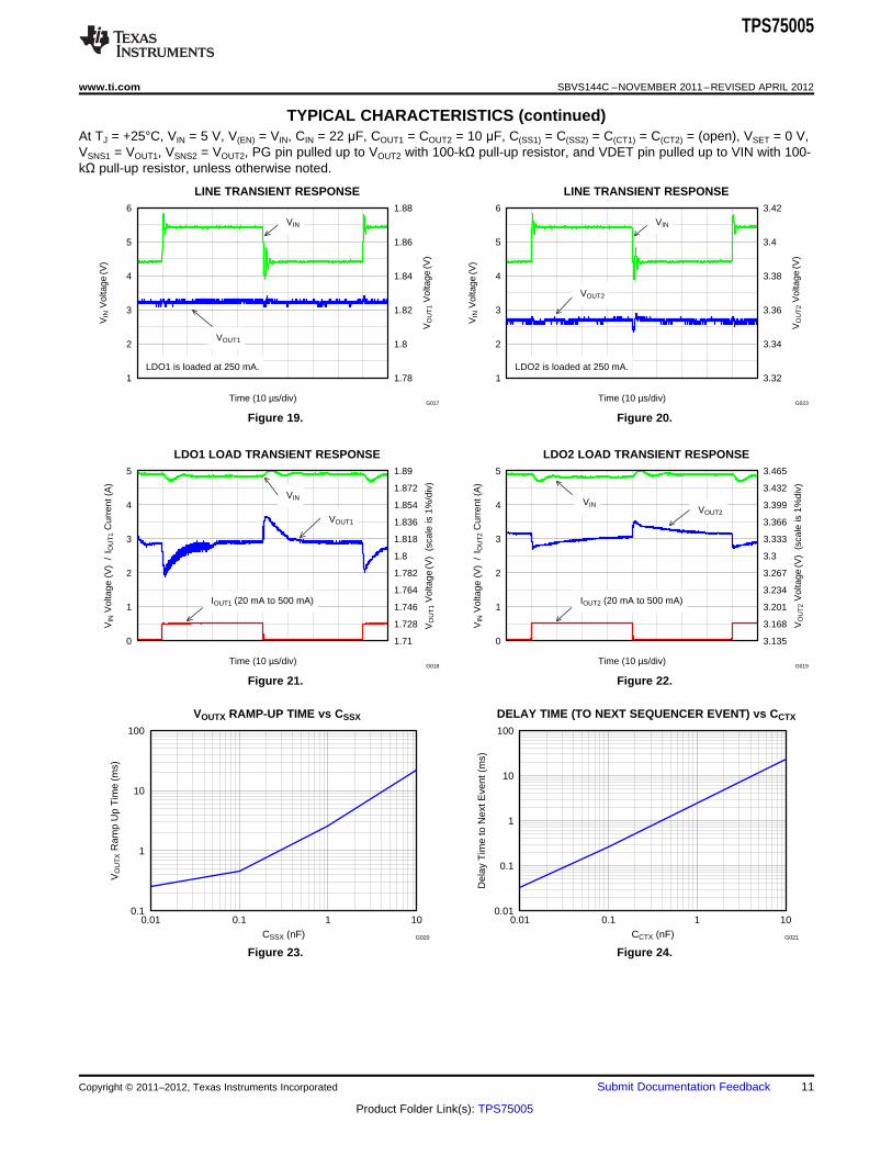
TYPICAL CHARACTERISTICS (continued)At TJ = +25°C, VIN = 5 V, V(EN) = VIN, CIN = 22 μF, COUT1 = COUT2 = 10 μF, C(SS1) = C(SS2) = C(CT1) = C(CT2) = (open), VSET = 0 V,VSNS1 = VOUT1, VSNS2 = VOUT2, PG pin pulled up to VOUT2 with 100-kΩ pull-up resistor, and VDET pin pulled up to VIN with 100-kΩ pull-up resistor, unless otherwise noted.
LINE TRANSIENT RESPONSE LINE TRANSIENT RESPONSE
Figure 19. Figure 20.
LDO1 LOAD TRANSIENT RESPONSE LDO2 LOAD TRANSIENT RESPONSE
Figure 21. Figure 22.
VOUTX RAMP-UP TIME vs CSSX DELAY TIME (TO NEXT SEQUENCER EVENT) vs CCTX
Figure 23. Figure 24.
Copyright © 2011–2012, Texas Instruments Incorporated Submit Documentation Feedback 11
Product Folder Link(s): TPS75005

2
3
4
5
6 7 8 9 10
1
11
14
13
12
15
21 20 19 18 1617
PWPD NC IN IN EN VMON
PGVSETSEQGNDGND
VDET
SS2
CT2
OUT2_S
OUT2
TEST
SS1
CT1
OUT1_S
OUT1
EN
R3
100 kW
VIN
C3
10 mF
VDDIO
C8
10 mF
VDD
R2
3.7 kW
R1
10 kWENC2
10 mF
VIN
VIN
Power Supply
R6
100 kW
PG
TPS75005
SBVS144C –NOVEMBER 2011–REVISED APRIL 2012 www.ti.com
APPLICATION INFORMATION
Design Guidelines
Figure 25 and Figure 26 show a basic schematic and PCB layout for applications using the internal defaultsettings for power-good delay and rise time of the LDO1 and LDO2 outputs at turn on. This configuration istypical for applications involving the targeted C2000 microcontrollers. The unused adjustment pins, CT1, CT2,SS1, and SS2, are left open or floating. Connecting the SEQ and VSET pins to ground selects the turn-onsequence and the output voltage of LDO1. The open-drain outputs at PG and VDET are pulled up to the inputvoltage through 100-kΩ resistors. VDET is connected to enable the TPS75005 when the input voltage exceedsthe SVS voltage set by resistor divider R1 and R2 to VMON. For highly dynamic loads, like that of the C2000microcontroller, the input capacitor, C2, and the output capacitors, C3 and C8, are specified to be 10-µF, X5R orX7R, 10-V, ceramic capacitors in order to meet transient performance requirements.
Figure 25. Configuration for F280x, F281x, F223x and F2833x Controllers(Set to automatically sequence C2000 when VIN > 4.5 V)
(C2, C3, C8 / 10-µF X5R ceramic capacitors)
12 Submit Documentation Feedback Copyright © 2011–2012, Texas Instruments Incorporated
Product Folder Link(s): TPS75005
TPS75005
www.ti.com SBVS144C –NOVEMBER 2011–REVISED APRIL 2012
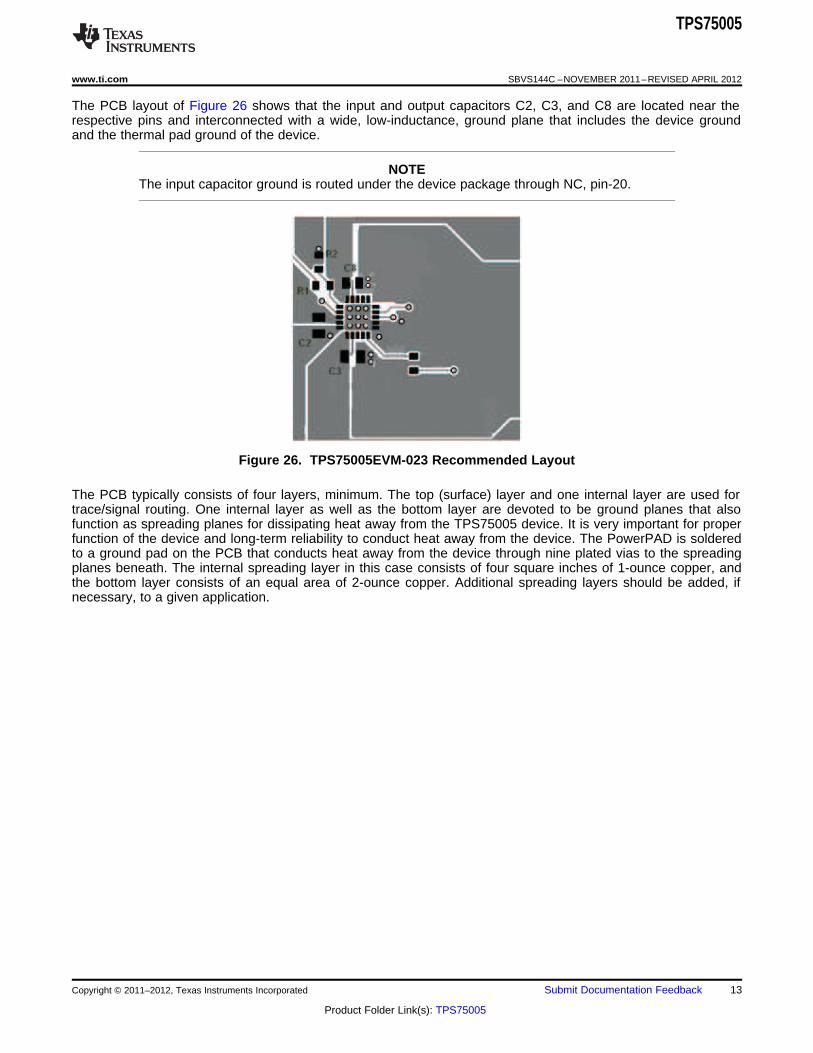
The PCB layout of Figure 26 shows that the input and output capacitors C2, C3, and C8 are located near therespective pins and interconnected with a wide, low-inductance, ground plane that includes the device groundand the thermal pad ground of the device.
NOTEThe input capacitor ground is routed under the device package through NC, pin-20.
Figure 26. TPS75005EVM-023 Recommended Layout
The PCB typically consists of four layers, minimum. The top (surface) layer and one internal layer are used fortrace/signal routing. One internal layer as well as the bottom layer are devoted to be ground planes that alsofunction as spreading planes for dissipating heat away from the TPS75005 device. It is very important for properfunction of the device and long-term reliability to conduct heat away from the device. The PowerPAD is solderedto a ground pad on the PCB that conducts heat away from the device through nine plated vias to the spreadingplanes beneath. The internal spreading layer in this case consists of four square inches of 1-ounce copper, andthe bottom layer consists of an equal area of 2-ounce copper. Additional spreading layers should be added, ifnecessary, to a given application.
Copyright © 2011–2012, Texas Instruments Incorporated Submit Documentation Feedback 13
Product Folder Link(s): TPS75005
LDO1
LDO2
OUT1
OUT1-S
OUT2
OUT2-S
10 Fm
VDDIO-n
VD
D-n
VDDIO-3
VD
D-3
VDDIO-2
VD
D-2
VDDIO-1
VD
D-1
0.1 Fm
0.1 Fm
0.1 Fm0.1 Fm 0.1 Fm
0.1 Fm
0.1 Fm
0.1 Fm
C2000
Controller
10 Fm
TPS75005
SBVS144C –NOVEMBER 2011–REVISED APRIL 2012 www.ti.com
LDO BLOCKS
The TPS75005 integrates two high-bandwidth LDOs for powering the VDD and VDDIO pins of the C2000controllers.
Input Capacitor
Although an input capacitor is not required for LDO stability, it is recommended to connect a 10-μF capacitoracross the input supply near the device. In addition to input capacitor consideration, pay attention to the printedcircuit board (PCB) design in order to reduce source impedance.
X5R- and X7R-type capacitors are highly recommended because they have minimal variation in value and ESRover temperature. Maximum ESR should be less than 1.0 Ω.
Output Capacitors
The TPS75005 is designed to be stable using standard ceramic capacitors with capacitance values 4.7 μF orgreater. In order to meet C2000 transient requirements, a 10-µF output capacitor at each of OUT1 and OUT2 isrecommended.
X5R- and X7R-type capacitors are highly recommended because they have minimal variation in value and ESRover temperature. Maximum ESR should be less than 1.0 Ω.
See the Sense Pins (OUT1_S AND OUT2_S) section for more details.
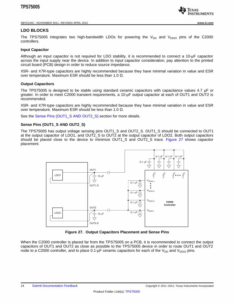
Sense Pins (OUT1_S AND OUT2_S)
The TPS75005 has output voltage sensing pins OUT1_S and OUT2_S. OUT1_S should be connected to OUT1at the output capacitor of LDO1, and OUT2_S to OUT2 at the output capacitor of LDO2. Both output capacitorsshould be placed close to the device to minimize OUT1_S and OUT2_S trace. Figure 27 shows capacitorplacement.
Figure 27. Output Capacitors Placement and Sense Pins
When the C2000 controller is placed far from the TPS75005 on a PCB, it is recommended to connect the outputcapacitors of OUT1 and OUT2 as close as possible to the TPS75005 device in order to route OUT1 and OUT2node to a C2000 controller, and to place 0.1-µF ceramic capacitors for each of the VDD and VDDIO pins.
14 Submit Documentation Feedback Copyright © 2011–2012, Texas Instruments Incorporated
Product Folder Link(s): TPS75005

t (s) =RAMPUP
C (F) + 110 10 (F)SSx ´-12
0.5 10 (A)´-6
´ 1.2 (V)
TPS75005
www.ti.com SBVS144C –NOVEMBER 2011–REVISED APRIL 2012
Soft-Start (SS1 and SS2)
The TPS75005 has a soft-start (or slow-start) function for LDO1 and LDO2 that work independently of oneanother. The ramp-up time for LDO1 and LDO2 is by default 260 µs due to the internal 110-pF capacitors. Byconnecting an external capacitor(s) at the SS1 and/or SS2 pins, the ramp-up time for the LDOs increasesproportionately by following this equation:
(1)
where:tRAMPUP = ramp up timeCSSx = external capacitor value at SS1 or SS2 pin
See Figure 23 for an actual measurement curve.
To ensure that these circuits are discharged during power down, the capacitors used can have a maximum valueof 10 nF approximately 24 ms of ramping time. When an application circuit must control a much larger timingperiod, use the supervisor delay setting in addition to the soft-start mechanism. See and find TSSx and Td(SVSx) inFigure 32. See the Delay Setting (CT1 and CT2) section for details.
All supported C2000 controllers work well with the TPS75005 default setting (without external soft-startcapacitors). In case a large number of output capacitors are connected for a specific application reason, it isrecommended to connect capacitors at SS1 and/or SS2 so that inrush current (into the TPS75005) does notcause a large input voltage droop. This can be mitigated by increasing the bulk capacitance at VIN.
NOTESS1 and SS2 are very high impedance nodes with very low values of constant currentsource. These two terminals cannot be monitored by regular oscilloscope probes.Connecting such regular probes to SS1 or SS2 changes the behavior of the soft-startfunction and no valid waveform can be monitored.
To monitor these terminals, use high-impedance probes, such as active FET probes.
Copyright © 2011–2012, Texas Instruments Incorporated Submit Documentation Feedback 15
Product Folder Link(s): TPS75005
TPS75005
SBVS144C –NOVEMBER 2011–REVISED APRIL 2012 www.ti.com
Internal Enable Signals and Pull-Down Switches
As shown in Figure 1, LDO1 is controlled by the internal signal EN1, and LDO2 is controlled by EN2. SW1 andSW2 are the inverse signals of EN1 and EN2, respectively. Whenever LDO1 and LDO2 are disabled, that meansEN1 and EN2 are logic-L, respectively. The corresponding output node(s) is discharged by an internal MOSFETand 360-Ω resistor controlled by SW1 and SW2.
These pull-down switches ensure that every power-down sequence is completed in a reasonable, finite time.See the Power-Down Monitoring section for a very important notice.
LDO1 Voltage Setting (VSET)
LDO1 can be configured as either a 1.8-V regulator or a 1.9-V regulator by the configuration of the VSET pin.When VSET is connected to ground, LDO1 outputs 1.8 V; when VSET is connected to the level of logic-H, LDO1outputs 1.9 V.
Current Limit
The TPS75005 internal current limit helps protect the regulator during unexpected fault conditions. During currentlimit, the output sources a fixed 900mA. If kept in current limit for an extended period of time, the device willthermally shutdown.
16 Submit Documentation Feedback Copyright © 2011–2012, Texas Instruments Incorporated
Product Folder Link(s): TPS75005
t (s) =d
C (F)SSx
0.5 10 (A)´-6
´ 1.2 (V)
TPS75005
www.ti.com SBVS144C –NOVEMBER 2011–REVISED APRIL 2012
MONITOR BLOCKS
Supply Voltage Supervisors (SVS1 and SVS2)
The TPS75005 integrates two supply voltage supervisors (SVSs) to monitor the VDD and VDDIO pins of the C2000controllers.
Delay Setting (CT1 and CT2)
The TPS75005 has a programmable delay function for both SVS1 and SVS2 that work independently of eachother. By default, both CT1 and CT2 are open, and both SVS1 and SVS2 take approximately 33 µs of delay timefrom the comparator trip event to its output. By connecting an external capacitor(s) at the CT1 and/or CT2 pins,the SVS delay time increases proportionately, as shown in the following equation:
(2)
where:td = delay timeCCTx = external capacitor value at CT1 or CT2 pin
See Figure 24 for an actual measurement curve.
For a long delay setting, use a very low leakage current capacitor such as X5R- or X7R-type to minimizecalculation errors from the previous equation.
All supported C2000 controllers work well with the TPS75005 default settings (without external delay capacitors).
NOTEAs with the SS1 and SS2 terminals, CT1 and CT2 are very high-impedance nodes withvery low values of constant current source. These two terminals cannot be monitored byregular oscilloscope probes. Connecting such regular probes to CT1 or CT2 changes thebehavior of the soft-start function and no valid waveform can be monitored.
To monitor these terminals, use high-impedance probes, such as active FET probes.
Spike Noise Sensitivity
Application Report SBVA033, TPS75005 Advanced Information: Voltage Monitor Noise Immunity, explainsTPS75005 noise immunity performance.
Power-Down Monitoring
The TPS75005 monitors both OUT1 and OUT2 to become 0.3 V in power-down sequence so that next power-upsequence starts from below 0.3 V.
See the SEQUENCER BLOCK section for more details.
NOTEIn any application circuit, a diode or two diodes in series should not be placed fromOUT1 (anode, 1.8 V) to OUT2 (cathode, 3.3 V). Such diode(s) prevent the TPS75005from pulling OUT2 below 0.3 V; the device stays in a power-down sequence and willnot power up again.
Copyright © 2011–2012, Texas Instruments Incorporated Submit Documentation Feedback 17
Product Folder Link(s): TPS75005
(SVS3 Detection Voltage Target) = 1.206 (V) ´R + R1 2
R2
R1
R2
SVS3
VDET
IN
VMON
10 Fm
5 V
100 kW
TPS75005
ENSequencer
Connect upperside of R1 to thevoltage monitored
TPS75005
SBVS144C –NOVEMBER 2011–REVISED APRIL 2012 www.ti.com
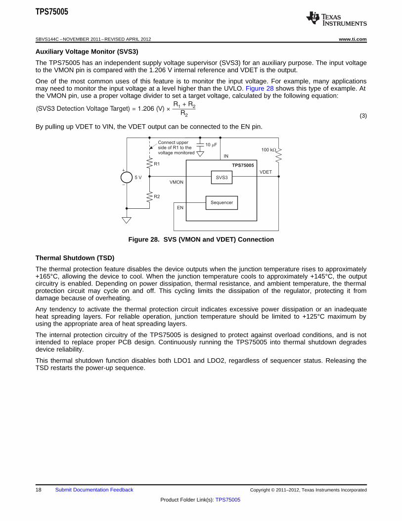
Auxiliary Voltage Monitor (SVS3)
The TPS75005 has an independent supply voltage supervisor (SVS3) for an auxiliary purpose. The input voltageto the VMON pin is compared with the 1.206 V internal reference and VDET is the output.
One of the most common uses of this feature is to monitor the input voltage. For example, many applicationsmay need to monitor the input voltage at a level higher than the UVLO. Figure 28 shows this type of example. Atthe VMON pin, use a proper voltage divider to set a target voltage, calculated by the following equation:
(3)
By pulling up VDET to VIN, the VDET output can be connected to the EN pin.
Figure 28. SVS (VMON and VDET) Connection
Thermal Shutdown (TSD)
The thermal protection feature disables the device outputs when the junction temperature rises to approximately+165°C, allowing the device to cool. When the junction temperature cools to approximately +145°C, the outputcircuitry is enabled. Depending on power dissipation, thermal resistance, and ambient temperature, the thermalprotection circuit may cycle on and off. This cycling limits the dissipation of the regulator, protecting it fromdamage because of overheating.
Any tendency to activate the thermal protection circuit indicates excessive power dissipation or an inadequateheat spreading layers. For reliable operation, junction temperature should be limited to +125°C maximum byusing the appropriate area of heat spreading layers.
The internal protection circuitry of the TPS75005 is designed to protect against overload conditions, and is notintended to replace proper PCB design. Continuously running the TPS75005 into thermal shutdown degradesdevice reliability.
This thermal shutdown function disables both LDO1 and LDO2, regardless of sequencer status. Releasing theTSD restarts the power-up sequence.
18 Submit Documentation Feedback Copyright © 2011–2012, Texas Instruments Incorporated
Product Folder Link(s): TPS75005
IN10 Fm
TPS75005
EN
Sequencer
TPS75005
www.ti.com SBVS144C –NOVEMBER 2011–REVISED APRIL 2012
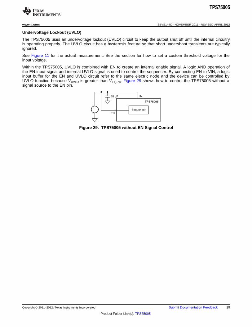
Undervoltage Lockout (UVLO)
The TPS75005 uses an undervoltage lockout (UVLO) circuit to keep the output shut off until the internal circuitryis operating properly. The UVLO circuit has a hysteresis feature so that short undershoot transients are typicallyignored.
See Figure 11 for the actual measurement. See the section for how to set a custom threshold voltage for theinput voltage.
Within the TPS75005, UVLO is combined with EN to create an internal enable signal. A logic AND operation ofthe EN input signal and internal UVLO signal is used to control the sequencer. By connecting EN to VIN, a logicinput buffer for the EN and UVLO circuit refer to the same electric node and the device can be controlled byUVLO function because VUVLO is greater than VIH(EN). Figure 29 shows how to control the TPS75005 without asignal source to the EN pin.
Figure 29. TPS75005 without EN Signal Control
Copyright © 2011–2012, Texas Instruments Incorporated Submit Documentation Feedback 19
Product Folder Link(s): TPS75005

0
1
2
3
4
5
6
Time
Vol
tage
(V
)
ENOUT1OUT2PG
G000
0
1
2
3
4
5
6
Time
Vol
tage
(V
)
ENOUT1OUT2PG
G000
TPS75005
SBVS144C –NOVEMBER 2011–REVISED APRIL 2012 www.ti.com
SEQUENCER BLOCK
The TPS75005 integrates a sequencer logic circuit to control the power-up and power-down sequences of thetwo output voltage rails (VDD and VDDIO) for C2000 controllers.
Application Report SBVA031, TPS75005 Advanced Information: Sequencer and State Machine, explains a statemachine of this sequencer logic in detail.
C2000 Power Sequencing
Depending on the C2000 controller series, the required power-up and power-down order of VDD and VDDIO canbe different, as shown in Table 1. Figure 30 and Figure 31 shows the typical waveforms of two differentsequencing cycles set by the SEQ pin.
Table 1. Required Power-Up and Power-Down Sequence of C2000 Controllers
POWER-UP ORDER POWER-DOWN ORDER
C2000 1ST CHANNEL 2ND CHANNEL 1ST CHANNEL 2ND CHANNEL TPS75005 TYPICALCONTROLLER TURNED ON TURNED ON TURNED OFF TURNED OFF SEQ SETTING WAVEFORM
F280x/F2801x VDD VDDIO VDDIO VDD Logic-L Figure 30
F281x VDDIO VDD VDD VDDIO Logic-H Figure 31
F2823x VDD VDDIO VDDIO VDD Logic-L Figure 30
F2833X VDD VDDIO VDDIO VDD Logic-L Figure 30
Figure 30. Power Sequence with SEQ = L Figure 31. Power Sequence with SEQ = H
20 Submit Documentation Feedback Copyright © 2011–2012, Texas Instruments Incorporated
Product Folder Link(s): TPS75005

TPS75005
www.ti.com SBVS144C –NOVEMBER 2011–REVISED APRIL 2012
Normal Power-Up and Power-Down Sequence
Figure 32 shows oscilloscope waveforms of the TPS75005 in a normal power-up and power-down sequence withSEQ = L. Refer to the time lines labeled Event A through Event H.
1. Before Event A, the TPS75005 is idle, waiting for an enable event.
(Power-Up Sequence Begins)
2. At Event A, EN goes to logic-H and the device immediately discharges a soft-start capacitor (CSS1) byusing a one-shot circuit. Then, the LDO1 soft-start circuit starts charging CSS1. The OUT1 voltage followsthe SS1 voltage. Time between Event A and Event B is defined as tSS1 and can be programmed by CSS1.
3. At Event B, the OUT1 voltage exceeds the VSVS1 threshold and the SVS1 delay circuit starts chargingCCT1. Time between Event B and Event C is defined as td(SVS1) and can be programmed by CCT1.
4. At Event C, the CT1 voltage exceeds the VCT1 threshold to discharge a soft-start capacitor (CSS2) using aone-shot circuit. Then, the LDO2 soft-start circuit starts charging CSS2. The OUT2 voltage follows theSS2 voltage. Time between Event C and Event D is defined as tSS2 and can be programmed by CSS2.
5. At Event D, the OUT2 voltage exceeds the VSVS2 threshold and the SVS2 delay circuit starts chargingCCT2. Time between Event D and Event E is defined as td(SVS2) and can be programmed by CCT2.
(Power-Up Sequence Ends)
6. At Event E, the CT2 voltage exceeds the VCT2 threshold and PG goes high to enable the C2000controller. The TPS75005 is up and running as long as a disable or an error event occurs.
(Power-Down Sequence Begins)
7. At Event F, EN goes to logic-L and the device immediately turns PG to logic-L so that the C2000controller is disabled. Then, an internal signal EN2 goes to logic-L in order to disable LDO2. Because theactive pull-down switch is enabled by SW2 (= EN2) signal, the OUT2 voltage starts decreasing (note thatthis ramp-down speed depends on the application circuits).
8. At Event G, the OUT2 voltage underruns the VDOWN2 threshold and an internal signal EN1 goes intologic-L in order to disable LDO1. Because the active pull-down switch is enabled by SW1 (= EN1) signal,the OUT1 voltage starts decreasing (note that this ramp-down speed is depends on the applicationcircuits).
9. At Event H, the OUT1 voltage underruns the VDOWN1 threshold to return back to the idle state.
(Power-Down Sequence Ends)
Copyright © 2011–2012, Texas Instruments Incorporated Submit Documentation Feedback 21
Product Folder Link(s): TPS75005

Event
A
Event
B
Event
C
Event
D
Event
E
Event
F
Event
G
Event
H
SS1
EN
OUT1
CT1
SS2
OUT2
CT2
PG
2%
2%
VSVS1
VSVS2
VCT2
VDOWN2
VDOWN1
VCT1
tD(SVS1)
tD(SVS2)
tSS1
tSS2
TPS75005
SBVS144C –NOVEMBER 2011–REVISED APRIL 2012 www.ti.com
Figure 32. Normal Power-Up and Power-Down Timing
22 Submit Documentation Feedback Copyright © 2011–2012, Texas Instruments Incorporated
Product Folder Link(s): TPS75005
P = (V V ) I-D IN OUT OUT
R =qJA
+125 C T° -A
PD
120
100
80
60
40
20
0
qJA
(C
/W)
°
0 1 2 3 4 5 6 7 8 9 10
Board Copper Area (in )2
qJA (RGW)
TPS75005
www.ti.com SBVS144C –NOVEMBER 2011–REVISED APRIL 2012
THERMAL INFORMATION
Power Dissipation
Knowing the device power dissipation and proper sizing of the thermal plane that is connected to the tab or padis critical to avoiding thermal shutdown and ensuring reliable operation.
Power dissipation of the device depends on input voltage and load conditions and can be calculated usingEquation 4:
(4)
Power dissipation can be minimized and greater efficiency can be achieved by using the lowest possible inputvoltage necessary to achieve the required output voltage regulation.
On the QFN (RGW) package, the primary conduction path for heat is through the exposed pad to the printedcircuit board (PCB). The pad can be connected to ground or be left floating; however, it should be attached to anappropriate amount of copper PCB area to ensure the device does not overheat. The maximum junction-to-ambient thermal resistance depends on the maximum ambient temperature, maximum device junctiontemperature, and power dissipation of the device and can be calculated using Equation 5:
(5)
Knowing the maximum RθJA, the minimum amount of PCB copper area needed for appropriate heat sinking canbe estimated using Figure 33.
NOTE: θJA value at a board size of 9-in2 (that is, 3-in × 3-in) is a JEDEC standard.
Figure 33. θJA vs Board Size
Figure 33 shows the variation of θJA as a function of ground plane copper area in the board. It is intended only asa guideline to demonstrate the effects of heat spreading in the ground plane and should not be used to estimateactual thermal performance in real application environments.
NOTE: When the device is mounted on an application PCB, it is strongly recommended to use ΨJT and ΨJB, asexplained in the Estimating Junction Temperature section.
Copyright © 2011–2012, Texas Instruments Incorporated Submit Documentation Feedback 23
Product Folder Link(s): TPS75005

Y YJT J T JT D: T = T + P·
Y YJB J B JB D: T = T + P·
12
10
8
6
4
2
0
YY
an
d(
C/W
)JT
JB
°
0 2 4 6 8 10
Board Copper Area (in )2
YJT (RGW)
YJB (RGW)
T on PCBB
T on of ICtopT
1mm
(a) Example RGW (QFN) Package Measurement
TPS75005
SBVS144C –NOVEMBER 2011–REVISED APRIL 2012 www.ti.com
Estimating Junction Temperature
Using the thermal metrics ΨJT and ΨJB, as shown in the Thermal Information table, the junction temperature canbe estimated with corresponding formulas (given in Equation 6). For backwards compatibility, an older θJC,Topparameter is listed as well.
Where:PD is the power dissipation shown by Equation 5TT is the temperature at the center-top of the deviceTB is the PCB temperature measured 1 mm away from the device on the PCB surface (as Figure 35shows). (6)
NOTE: Both TT and TB can be measured on actual application boards using an infrared thermometer.
For more information about measuring TT and TB, see Application Report SBVA025, Using New Thermal Metrics,available for download at www.ti.com.
By looking at Figure 34, the new thermal metrics (ΨJT and ΨJB) have very little dependency on board size. Thatis, using ΨJT or ΨJB with Equation 6 is a good way to estimate TJ by simply measuring TT or TB, regardless of theapplication board size.
Figure 34. ΨJT and ΨJB vs Board Size
For a more detailed discussion of why TI does not recommend using θJC(top) to determine thermal characteristics,refer to Application Report SBVA025, Using New Thermal Metrics, available for download at www.ti.com. Forfurther information, refer to Application Report SPRA953, IC Package Thermal Metrics, also available on the TIwebsite.
Figure 35. Measuring Points for TT and TB
24 Submit Documentation Feedback Copyright © 2011–2012, Texas Instruments Incorporated
Product Folder Link(s): TPS75005

TPS75005
www.ti.com SBVS144C –NOVEMBER 2011–REVISED APRIL 2012
REVISION HISTORY
NOTE: Page numbers for previous revisions may differ from page numbers in the current version.
Changes from Revision B (March 2012) to Revision C Page
• Changed Voltage Information table ...................................................................................................................................... 2
• Added new note 2 to Thermal Information table .................................................................................................................. 3
• Changed note 3(b) copper coverage value from 20% to 4% ............................................................................................... 3
• Changed test condition for tD(SVS1) parameter ....................................................................................................................... 4
• Changed test condition for tD(SVS2) parameter ....................................................................................................................... 5
• Changed functional block diagram ....................................................................................................................................... 7
Changes from Revision A (February 2012) to Revision B Page
• Changed Thermal Information table values .......................................................................................................................... 3
• Changed functional block diagram ....................................................................................................................................... 7
Changes from Original (November 2011) to Revision A Page
• Changed all "PowerPAD" to "thermal pad". .......................................................................................................................... 1
• Added application report links to Description section ........................................................................................................... 1
• Changed "VIN" to "IN" in front page diagram ....................................................................................................................... 1
• Changed "VIN" to "IN" ............................................................................................................................................................ 6
• Changed "VIN" to "input voltage" ........................................................................................................................................ 12
• Changed caption for Figure 25 ........................................................................................................................................... 12
• Changed Voltage Monitor Blocks section title and updated subsection order ................................................................... 17
• Changed "VIN" to "IN" in Figure 28 .................................................................................................................................... 18
• Changed "VIN" to "IN" in Figure 29 .................................................................................................................................... 19
Copyright © 2011–2012, Texas Instruments Incorporated Submit Documentation Feedback 25
Product Folder Link(s): TPS75005

PACKAGE OPTION ADDENDUM
www.ti.com 10-Dec-2020
Addendum-Page 1
PACKAGING INFORMATION
Orderable Device Status(1)
Package Type PackageDrawing
Pins PackageQty
Eco Plan(2)
Lead finish/Ball material
(6)
MSL Peak Temp(3)
Op Temp (°C) Device Marking(4/5)
Samples
TPS75005RGWR NRND VQFN RGW 20 3000 RoHS & Green NIPDAU Level-2-260C-1 YEAR -40 to 125 PPMQ
TPS75005RGWT NRND VQFN RGW 20 250 RoHS & Green NIPDAU Level-2-260C-1 YEAR -40 to 125 PPMQ (1) The marketing status values are defined as follows:ACTIVE: Product device recommended for new designs.LIFEBUY: TI has announced that the device will be discontinued, and a lifetime-buy period is in effect.NRND: Not recommended for new designs. Device is in production to support existing customers, but TI does not recommend using this part in a new design.PREVIEW: Device has been announced but is not in production. Samples may or may not be available.OBSOLETE: TI has discontinued the production of the device.
(2) RoHS: TI defines "RoHS" to mean semiconductor products that are compliant with the current EU RoHS requirements for all 10 RoHS substances, including the requirement that RoHS substancedo not exceed 0.1% by weight in homogeneous materials. Where designed to be soldered at high temperatures, "RoHS" products are suitable for use in specified lead-free processes. TI mayreference these types of products as "Pb-Free".RoHS Exempt: TI defines "RoHS Exempt" to mean products that contain lead but are compliant with EU RoHS pursuant to a specific EU RoHS exemption.Green: TI defines "Green" to mean the content of Chlorine (Cl) and Bromine (Br) based flame retardants meet JS709B low halogen requirements of <=1000ppm threshold. Antimony trioxide basedflame retardants must also meet the <=1000ppm threshold requirement.
(3) MSL, Peak Temp. - The Moisture Sensitivity Level rating according to the JEDEC industry standard classifications, and peak solder temperature.
(4) There may be additional marking, which relates to the logo, the lot trace code information, or the environmental category on the device.
(5) Multiple Device Markings will be inside parentheses. Only one Device Marking contained in parentheses and separated by a "~" will appear on a device. If a line is indented then it is a continuationof the previous line and the two combined represent the entire Device Marking for that device.
(6) Lead finish/Ball material - Orderable Devices may have multiple material finish options. Finish options are separated by a vertical ruled line. Lead finish/Ball material values may wrap to twolines if the finish value exceeds the maximum column width.
Important Information and Disclaimer:The information provided on this page represents TI's knowledge and belief as of the date that it is provided. TI bases its knowledge and belief on informationprovided by third parties, and makes no representation or warranty as to the accuracy of such information. Efforts are underway to better integrate information from third parties. TI has taken andcontinues to take reasonable steps to provide representative and accurate information but may not have conducted destructive testing or chemical analysis on incoming materials and chemicals.TI and TI suppliers consider certain information to be proprietary, and thus CAS numbers and other limited information may not be available for release.
In no event shall TI's liability arising out of such information exceed the total purchase price of the TI part(s) at issue in this document sold by TI to Customer on an annual basis.
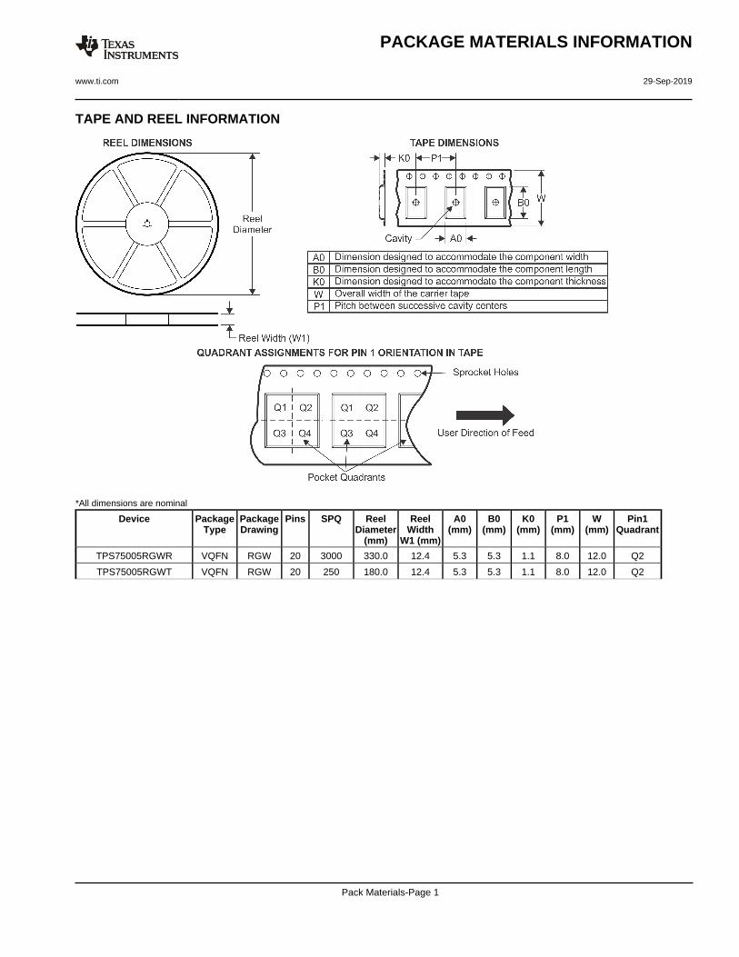
TAPE AND REEL INFORMATION
*All dimensions are nominal
Device PackageType
PackageDrawing
Pins SPQ ReelDiameter
(mm)
ReelWidth
W1 (mm)
A0(mm)
B0(mm)
K0(mm)
P1(mm)
W(mm)
Pin1Quadrant
TPS75005RGWR VQFN RGW 20 3000 330.0 12.4 5.3 5.3 1.1 8.0 12.0 Q2
TPS75005RGWT VQFN RGW 20 250 180.0 12.4 5.3 5.3 1.1 8.0 12.0 Q2
PACKAGE MATERIALS INFORMATION
www.ti.com 29-Sep-2019
Pack Materials-Page 1
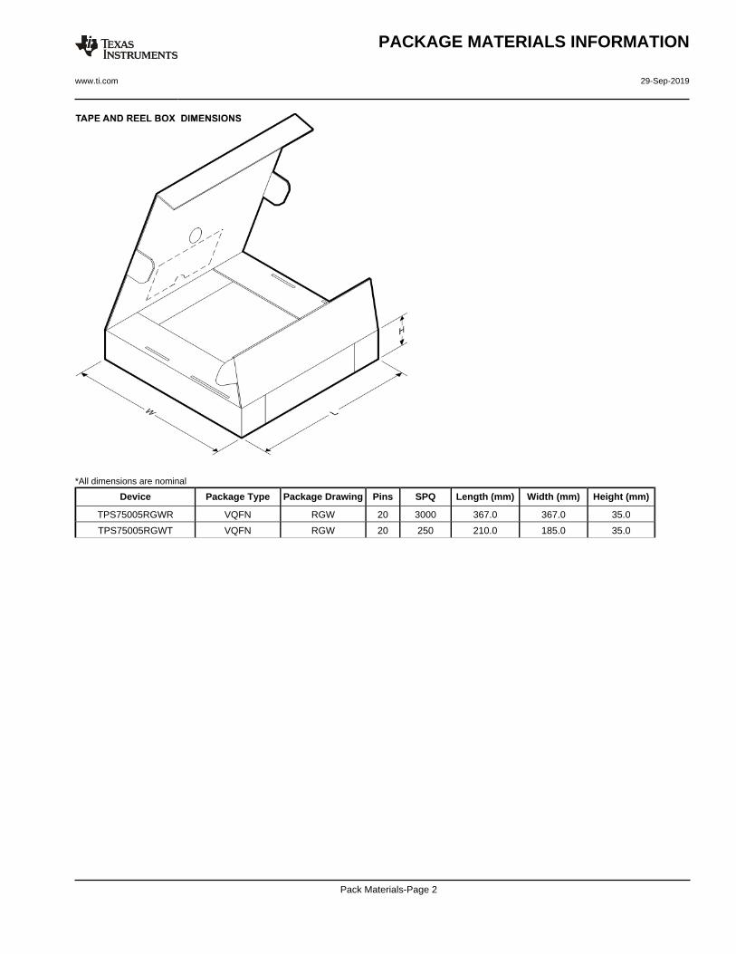
*All dimensions are nominal
Device Package Type Package Drawing Pins SPQ Length (mm) Width (mm) Height (mm)
TPS75005RGWR VQFN RGW 20 3000 367.0 367.0 35.0
TPS75005RGWT VQFN RGW 20 250 210.0 185.0 35.0
PACKAGE MATERIALS INFORMATION
www.ti.com 29-Sep-2019
Pack Materials-Page 2
www.ti.com
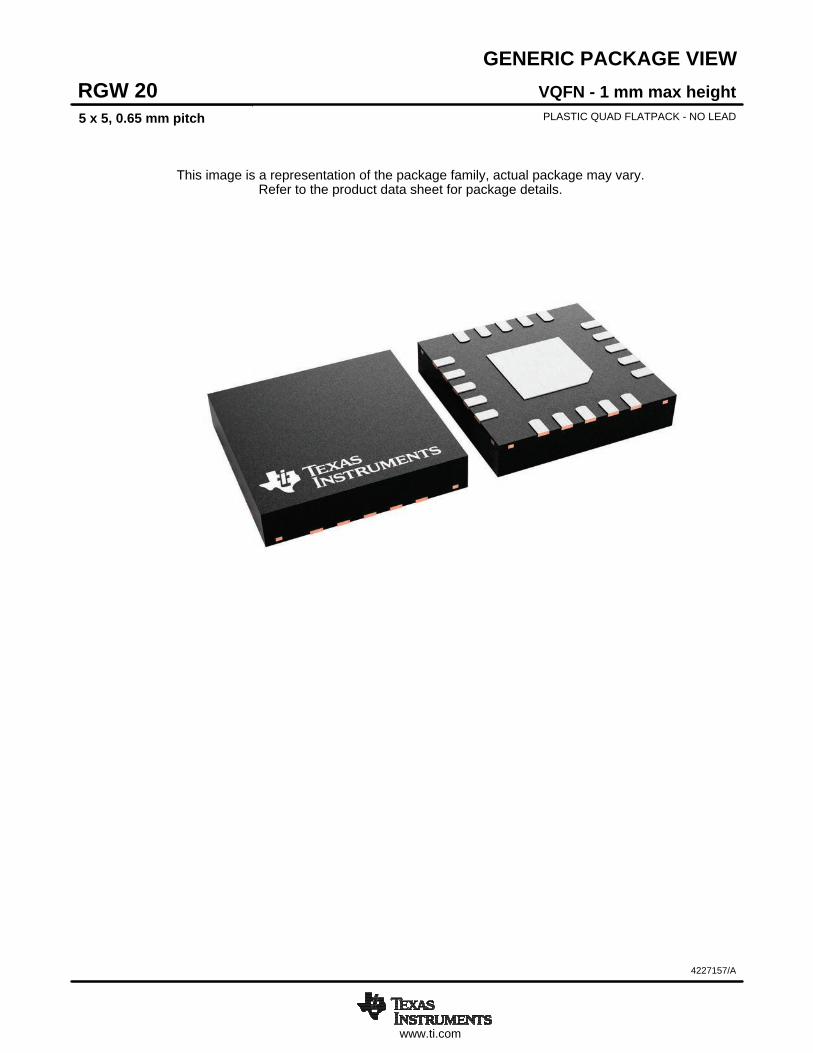
GENERIC PACKAGE VIEW
This image is a representation of the package family, actual package may vary.Refer to the product data sheet for package details.
VQFN - 1 mm max heightRGW 20PLASTIC QUAD FLATPACK - NO LEAD5 x 5, 0.65 mm pitch
4227157/A

NOTES:
1. All linear dimensions are in millimeters. Any dimensions in parenthesis are for reference only. Dimensioning and tolerancing
per ASME Y14.5M.
2. This drawing is subject to change without notice.
3. The package thermal pad must be soldered to the printed circuit board for optimal thermal and mechanical performance.
PACKAGE OUTLINE
4219039/A 06/2018
www.ti.com
VQFN - 1 mm max height
PLASTIC QUAD FLATPACK-NO LEAD
RGW0020A
C
0.08 C
0.1 C A B
0.05 C
B
SYMM
SYMM
PIN 1 INDEX AREA
5.1
4.9
5.1
4.9
1 MAX
0.05
0.00
SEATING PLANE
(0.1) TYP
3.15±0.1
2X
2.6
16X 0.65
20X
0.65
0.45
20X
0.36
0.26
2X 2.6
PIN1 ID
(OPTIONAL)
1
5
15
11
21
610
1620

NOTES: (continued)
4. This package is designed to be soldered to a thermal pad on the board. For more information, see Texas Instruments literature
number SLUA271 (www.ti.com/lit/slua271).5. Vias are optional depending on application, refer to device data sheet. If any vias are implemented, refer to their locations shown
on this view. It is recommended that vias under paste be filled, plugged or tented.
EXAMPLE BOARD LAYOUT
4219039/A 06/2018
www.ti.com
VQFN - 1 mm max height
RGW0020A
PLASTIC QUAD FLATPACK-NO LEAD
SYMM
SYMM
LAND PATTERN EXAMPLE
SCALE: 15X
0.07 MAX
ALL AROUND
0.07 MIN
ALL AROUND
NON SOLDER MASK
DEFINED
(PREFERRED)
SOLDER MASK
DEFINED
METAL
SOLDER MASK
OPENING
SOLDER MASK
OPENING
METAL UNDER
SOLDER MASK
EXPOSED METAL
EXPOSED METAL
SOLDER MASK DETAILS
( 3.15)
(2.6)
(4.65)
(2.6)
16X (0.65)
(4.65)
20X (0.75)
20X (0.31)
(Ø0.2) VIA
TYP
(R0.05) TYP
(1.325)
(1.325)
1
5
6
10
11
15
1620
21
NOTES: (continued)
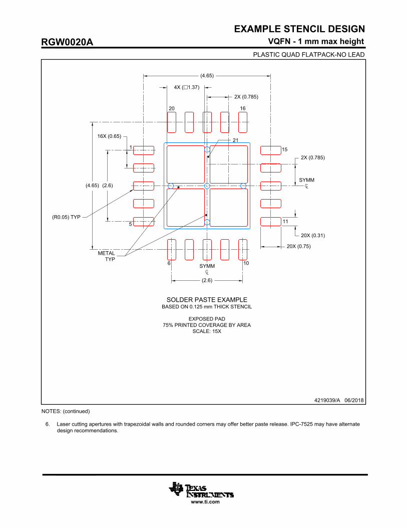
6. Laser cutting apertures with trapezoidal walls and rounded corners may offer better paste release. IPC-7525 may have alternate
design recommendations.
EXAMPLE STENCIL DESIGN
4219039/A 06/2018
www.ti.com
VQFN - 1 mm max height
RGW0020A
PLASTIC QUAD FLATPACK-NO LEAD
SOLDER PASTE EXAMPLE
BASED ON 0.125 mm THICK STENCIL
EXPOSED PAD
75% PRINTED COVERAGE BY AREA
SCALE: 15X
SYMM
SYMM
4X ( 1.37)
(2.6)
(4.65)
(2.6)
16X (0.65)
(4.65)
20X (0.75)
20X (0.31)
(R0.05) TYP
2X (0.785)
2X (0.785)
1
5
6 10
11
15
1620
21
METAL
TYP
IMPORTANT NOTICE AND DISCLAIMERTI PROVIDES TECHNICAL AND RELIABILITY DATA (INCLUDING DATA SHEETS), DESIGN RESOURCES (INCLUDING REFERENCE DESIGNS), APPLICATION OR OTHER DESIGN ADVICE, WEB TOOLS, SAFETY INFORMATION, AND OTHER RESOURCES “AS IS” AND WITH ALL FAULTS, AND DISCLAIMS ALL WARRANTIES, EXPRESS AND IMPLIED, INCLUDING WITHOUT LIMITATION ANY IMPLIED WARRANTIES OF MERCHANTABILITY, FITNESS FOR A PARTICULAR PURPOSE OR NON-INFRINGEMENT OF THIRD PARTY INTELLECTUAL PROPERTY RIGHTS.These resources are intended for skilled developers designing with TI products. You are solely responsible for (1) selecting the appropriate TI products for your application, (2) designing, validating and testing your application, and (3) ensuring your application meets applicable standards, and any other safety, security, regulatory or other requirements.These resources are subject to change without notice. TI grants you permission to use these resources only for development of an application that uses the TI products described in the resource. Other reproduction and display of these resources is prohibited. No license is granted to any other TI intellectual property right or to any third party intellectual property right. TI disclaims responsibility for, and you will fully indemnify TI and its representatives against, any claims, damages, costs, losses, and liabilities arising out of your use of these resources.TI’s products are provided subject to TI’s Terms of Sale or other applicable terms available either on ti.com or provided in conjunction with such TI products. TI’s provision of these resources does not expand or otherwise alter TI’s applicable warranties or warranty disclaimers for TI products.TI objects to and rejects any additional or different terms you may have proposed. IMPORTANT NOTICE
Mailing Address: Texas Instruments, Post Office Box 655303, Dallas, Texas 75265Copyright © 2021, Texas Instruments Incorporated


