
Intermodulation Distortion(IMD) MeasurementsUsing the 37300 Series Vector Network AnalyzerApplication Note

2
OVERVIEWIntermodulation distortion (IMD) has become increasinglyimportant in microwave and RF amplifier design. Asmodulation techniques become more sophisticated, greaterperformance is required from amplifier and receiver circuits.Unlike harmonic and second order distortion products, thirdorder intermodulation distortion products (IP3) are in-bandand cannot be easily filtered. Therefore, innovative designsusing special feedback and feedforward techniques have beendeveloped that greatly improve IMD performance. Thisenables amplifiers to operate at much higher output levelswhile maintaining low distortion products. As a device’sintermodulation distortion is improved, greater demands aremade on measurement equipment. This Application Notediscusses the concept of measuring third order products usingthe Anritsu 373XX series of Vector Network Analyzers, inconjunction with Anritsu 68XXX or 69XXX synthesizers.Second order products will be shown for completeness, butemphasis is placed on the measurement of third order productsand the calculations required to determine the sweptthird order intercept (TOI) point.
Harmonic DistortionHarmonic distortion can be defined as a single-tone distortionproduct caused by device non-linearity. When a non-lineardevice is stimulated by a signal at frequency f1, spuriousoutput signals can be generated at the harmonic frequencies2f1, 3f1, 4f1,...Nf1. The order of the distortion product is givenby the frequency multiplier; for example, the second harmonicis a second order product, the third harmonic is a third orderproduct, and the Nth harmonic is the Nth order product.Harmonics are usually measured in dBc, dB below the carrier(fundamental) output signal (see Figure 1).
Figure 1
Intermodulation DistortionIntermodulation distortion is a multi-tone distortion productthat results when two or more signals are present at the inputof a non-linear device. All semiconductors inherently exhibita degree of non-linearity, even those which are biased for“linear” operation. The spurious products which are generateddue to the non-linearity of a device are mathematically relatedto the original input signals. Analysis of several stimulus tonescan become very complex so it is a common practice to limitthe analysis to two tones. The frequencies of the two-toneintermodulation products can be computed by the equation:
M f1 ± N f2, where M, N = 0, 1, 2, 3, .....
The order of the distortion product is given by the sum ofM + N. The second order intermodulation products of twosignals at f1 and f2 would occur at f1 + f2, f2 – f1, 2f1 and 2f2
(see Figure 2 below).
Figure 2
Third order intermodulation products of the two signals, f1 andf2, would be:
2f1 + f22f1 – f2f1 + 2f2f1 – 2f2
Where 2f1 is the second harmonic of f1 and 2f2 is the secondharmonic of f2.
Second Order Intermodulation Distortion
f2-f1 f1+f2f1 f2 2f1 2f2Frequency
Amplitude
x dBc y dBc
Fundamental
Harmonic Distortion
Frequency
f1 3f12f1
Amplitude
3
Mathematically the f2 – 2f1 and f1 – 2f2 intermodulationproduct calculation could result in a “negative” frequency.However, it is the absolute value of these calculations that isof concern. The absolute value of f1 – 2f2 is the same as theabsolute value of 2f2 – f1. It is common to talk about thethird order intermodulation products as being 2f1 ± f2
and 2f2 ± f1.
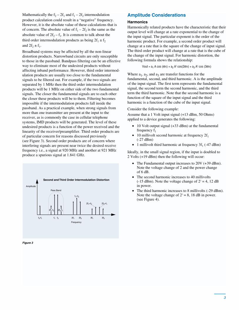
Broadband systems may be affected by all the non-lineardistortion products. Narrowband circuits are only susceptibleto those in the passband. Bandpass filtering can be an effectiveway to eliminate most of the undesired products withoutaffecting inband performance. However, third order intermod-ulation products are usually too close to the fundamentalsignals to be filtered out. For example, if the two signals areseparated by 1 MHz then the third order intermodulationproducts will be 1 MHz on either side of the two fundamentalsignals. The closer the fundamental signals are to each otherthe closer these products will be to them. Filtering becomesimpossible if the intermodulation products fall inside thepassband. As a practical example, when strong signals frommore than one transmitter are present at the input to thereceiver, as is commonly the case in cellular telephonesystems, IMD products will be generated. The level of theseundesired products is a function of the power received and thelinearity of the receiver/preamplifier. Third order products areof particular concern for reasons discussed previously(see Figure 3). Second order products are of concern whereinterfering signals are present near twice the desired receivefrequency i.e., a signal at 920 MHz and another at 921 MHzproduce a spurious signal at 1.841 GHz.
Figure 3
Amplitude ConsiderationsHarmonicsHarmonically related products have the characteristic that theiroutput level will change at a rate exponential to the change ofthe input signal. The particular exponent is the order of theharmonic product. For example, a second order product willchange at a rate that is the square of the change of input signal.The third order product will change at a rate that is the cube ofthe change of the input signal. For harmonic distortion, thefollowing formula shows the relationship:
Vout = a1 A cos (ϖτ) + a2 A2 cos(2ϖτ) + a3 A3 cos (3ϖτ)
Where a1, a2, and a3 are transfer functions for thefundamental, second, and third harmonic. A is the amplitudeof the input signal. The first term represents the fundamentalsignal, the second term the second harmonic, and the thirdterm the third harmonic. Note that the second harmonic is afunction of the square of the input signal and the thirdharmonic is a function of the cube of the input signal.
Consider the following example:
Assume that a 1 Volt input signal (+13 dBm, 50 Ohms)applied to a device generates the following:
• 10 Volt output signal (+33 dBm) at the fundamentalfrequency f1
• 10 millivolt second harmonic at frequency 2f1(-27 dBm)
• 1 millivolt third harmonic at frequency 3f1 (-47 dBm)
Ideally, in the small signal region, if the input is doubled to2 Volts (+19 dBm) then the following will occur:
• The Fundamental output increases to 20V (+39 dBm).Note the voltage change of 2 and the power changeof 6 dB.
• The second harmonic increases to 40 millivolts (-15 dBm). Note the voltage change of 22 = 4, 12 dBin power.
• The third harmonic increases to 8 millivolts (-29 dBm).Note the voltage change of 23 = 8, 18 dB in power. (see Figure 4).
Second and Third Order Intermodulation Distortion
2f1-f2
f1+f2
f1 f2 3f1 3f22f1 2f2f2-f1
2f2-f1
2f2+f12f1+f2
Pass Band
Frequency
Amplitude
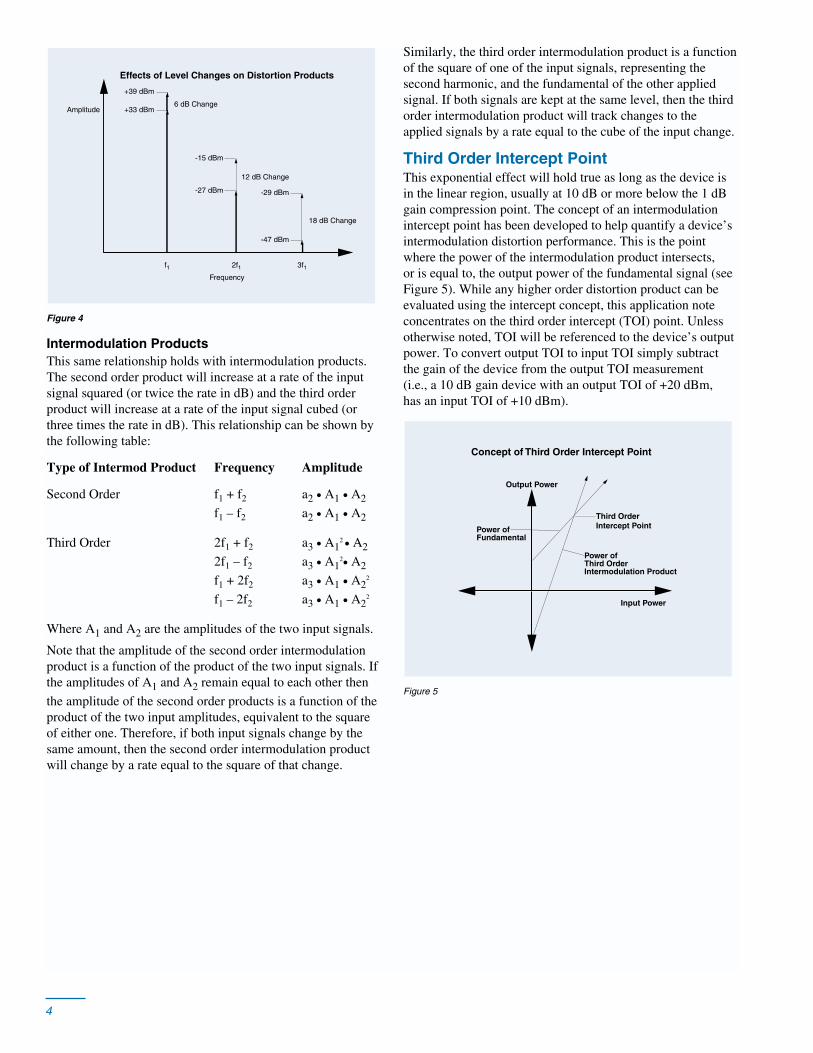
Figure 4
Intermodulation ProductsThis same relationship holds with intermodulation products.The second order product will increase at a rate of the inputsignal squared (or twice the rate in dB) and the third orderproduct will increase at a rate of the input signal cubed (orthree times the rate in dB). This relationship can be shown bythe following table:
Type of Intermod Product Frequency Amplitude
Second Order f1 + f2 a2 • A1 • A2
f1 – f2 a2 • A1 • A2
Third Order 2f1 + f2 a3 • A12 • A2
2f1 – f2 a3 • A12• A2
f1 + 2f2 a3 • A1 • A22
f1 – 2f2 a3 • A1 • A22
Where A1 and A2 are the amplitudes of the two input signals.
Note that the amplitude of the second order intermodulationproduct is a function of the product of the two input signals. Ifthe amplitudes of A1 and A2 remain equal to each other then
the amplitude of the second order products is a function of theproduct of the two input amplitudes, equivalent to the squareof either one. Therefore, if both input signals change by thesame amount, then the second order intermodulation productwill change by a rate equal to the square of that change.
Similarly, the third order intermodulation product is a functionof the square of one of the input signals, representing thesecond harmonic, and the fundamental of the other appliedsignal. If both signals are kept at the same level, then the thirdorder intermodulation product will track changes to theapplied signals by a rate equal to the cube of the input change.
Third Order Intercept PointThis exponential effect will hold true as long as the device isin the linear region, usually at 10 dB or more below the 1 dBgain compression point. The concept of an intermodulationintercept point has been developed to help quantify a device’sintermodulation distortion performance. This is the pointwhere the power of the intermodulation product intersects,or is equal to, the output power of the fundamental signal (seeFigure 5). While any higher order distortion product can beevaluated using the intercept concept, this application noteconcentrates on the third order intercept (TOI) point. Unlessotherwise noted, TOI will be referenced to the device’s outputpower. To convert output TOI to input TOI simply subtractthe gain of the device from the output TOI measurement(i.e., a 10 dB gain device with an output TOI of +20 dBm,has an input TOI of +10 dBm).
Figure 5
Concept of Third Order Intercept Point
Output Power
Input Power
Third OrderIntercept Point
Power of Third Order Intermodulation Product
Power of Fundamental
Effects of Level Changes on Distortion Products
2f1f1 3f1
+39 dBm
+33 dBm
-15 dBm
-27 dBm -29 dBm
-47 dBm
18 dB Change
6 dB Change
12 dB Change
Frequency
Amplitude
4
5
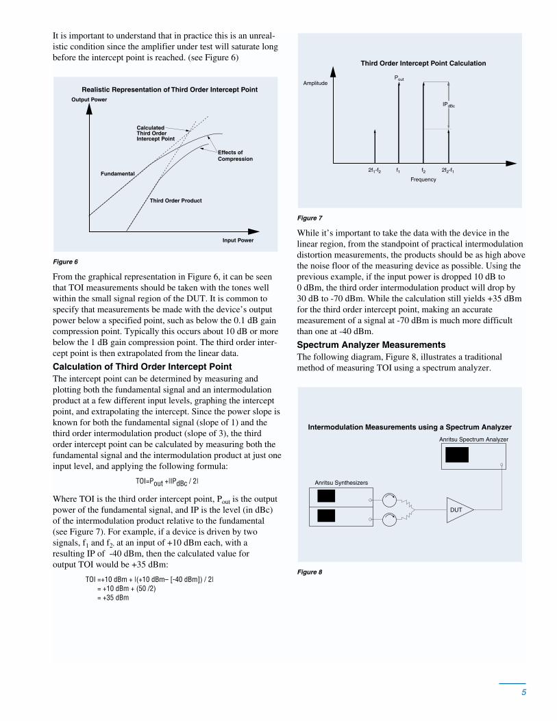
It is important to understand that in practice this is an unreal-istic condition since the amplifier under test will saturate longbefore the intercept point is reached. (see Figure 6)
Figure 6
From the graphical representation in Figure 6, it can be seenthat TOI measurements should be taken with the tones wellwithin the small signal region of the DUT. It is common tospecify that measurements be made with the device’s outputpower below a specified point, such as below the 0.1 dB gaincompression point. Typically this occurs about 10 dB or morebelow the 1 dB gain compression point. The third order inter-cept point is then extrapolated from the linear data.
Calculation of Third Order Intercept PointThe intercept point can be determined by measuring andplotting both the fundamental signal and an intermodulationproduct at a few different input levels, graphing the interceptpoint, and extrapolating the intercept. Since the power slope isknown for both the fundamental signal (slope of 1) and thethird order intermodulation product (slope of 3), the thirdorder intercept point can be calculated by measuring both thefundamental signal and the intermodulation product at just oneinput level, and applying the following formula:
TOI=Pout +|IPdBc / 2|
Where TOI is the third order intercept point, Pout is the outputpower of the fundamental signal, and IP is the level (in dBc)of the intermodulation product relative to the fundamental(see Figure 7). For example, if a device is driven by twosignals, f1 and f2, at an input of +10 dBm each, with aresulting IP of -40 dBm, then the calculated value foroutput TOI would be +35 dBm:
TOI =+10 dBm + |(+10 dBm– [-40 dBm]) / 2| = +10 dBm + (50 /2)= +35 dBm
Figure 7
While it’s important to take the data with the device in thelinear region, from the standpoint of practical intermodulationdistortion measurements, the products should be as high abovethe noise floor of the measuring device as possible. Using theprevious example, if the input power is dropped 10 dB to0 dBm, the third order intermodulation product will drop by30 dB to -70 dBm. While the calculation still yields +35 dBmfor the third order intercept point, making an accuratemeasurement of a signal at -70 dBm is much more difficultthan one at -40 dBm.
Spectrum Analyzer Measurements The following diagram, Figure 8, illustrates a traditionalmethod of measuring TOI using a spectrum analyzer.
Figure 8
Anritsu Spectrum Analyzer
Anritsu Synthesizers
DUT
Intermodulation Measurements using a Spectrum Analyzer
IPdBc
Third Order Intercept Point Calculation
Frequency
2f2-f12f1-f2
Amplitude
f1 f2
Pout
Output Power
Fundamental
Third Order Product
Effects of Compression
Calculated Third Order Intercept Point
Realistic Representation of Third Order Intercept Point
Input Power

It is important to minimize residual intermodulation distortioncaused by the measurement equipment. Without some form ofisolation, the two sources can intermodulate with each other,either by the non-linear characteristics of the source outputcircuitry or leakage into the phase lock circuits. If an inter-modulation measurement of -60 dBc is attempted with aresidual intermodulation signal of -70 dBc, then the error willbe about ±2.5 dB. Ferrite isolators or attenuators can be usedfor decoupling the sources, however, attenuators are muchwider in bandwidth than ferrites and are more readily avail-able. It’s also important to make sure that the receiver is notoverdriven, causing intermodulation products on its own.
By carefully setting the RF attenuation and display scaling,spectrum analyzers can make accurate measurements ofthe fundamental signals, however, errors can be as high as±0.5 dB depending on the frequency range for the highlevel f1 and f2 signals. Another source of error is the displayand marker accuracy, which can be as high as ±2 dB over thefull amplitude range of a spectrum analyzer. Insertion loss ofinterconnect cabling and pads will also cause measurementerror. The frequency response and power measurement errorscan be minimized by calibrating the system with a powermeter, but this complicates the system and usually requiresan external instrument controller with software. Spectrumanalyzers usually have the greatest accuracy when measuringthe desired signal at the top of the display. Signals measuredbelow that point usually have an error that is inverselyproportional to the level of the signal, relative to the top of thedisplay. However, if the spectrum analyzer is set to have theintermodulation product at the top of the display, then eitherthe mixer or log amplifiers will be overdriven by the presenceof the much larger fundamental signals. Therefore, it is usuallyrecommended that the display not be changed from thesettings necessary to make accurate measurements of thefundamental products. This can present significant demandson accurate spectrum analyzer measurements. Some of thenew feedforward cellular amplifiers have TOI specificationsgreater than 30 dB above the 1 dB gain compression point.If one assumes that TOI measurements are made at an output10 dB to 15 dB below the 1 dB gain compression point, thenthis represents an output power of 40 dB or more below theTOI point. A drop of 40 dB in fundamental output power willcause the third order intermodulation product to decreaseby 110 dB yielding a maximum intermodulation product of-80 dBc. This is a very demanding measurement for anymeasurement device. Techniques have been developed byusing discrete notch filters to significantly reduce thefundamental signals so that RF attenuation can be reduced,improving measurement accuracy. However, these measure-ments are slow, require switched filters, and require quitecomplex calibration techniques. They are also limited by thefilter skirts making narrow band measurements difficult.Moreover, individual filters must be used for each frequencymeasured, limiting the number of points that can be measuredon any particular device.
Swept TOI Measurements Using the 37300 SeriesVector Network AnalyzerThe 373XX series VNAs offer a unique approach to TOImeasurements across the full frequency range of theinstrument (see Figure 9). With a 373XX VNA, and 68XXXor 69XXX series Anritsu synthesizers, accurate wide dynamicrange measurements of any signals that are mathematicallyrelated to the fundamental signals can be made. This includesharmonics, amplifier intermodulation products, small signalmixing products, and mixer IM products. This capability ismade possible by the 373XX’s receiver design and the abilityto control two of the above mentioned synthesizers simultane-ously. Power level look-up tables for each synthesizer can bestored in the synthesizers themselves, thereby providing flatsignals at the input to the DUT. The power level at the synthe-sizer output port is controlled very tightly and is typically heldto within ±0.1 dB at 0 dBm output.
Figure 9
Since TOI calculations require the data to be entered interms of power, and a VNA is normally is used for ratiomeasurements, accurate absolute power measurements requirethe procedure described in the Appendix.
It should be pointed out, that there is no built-in pre-selectionavailable in a VNA. Frequency selectivity comes as a result ofIF rejection. The measurements described here capitalize onthe fact that the frequencies of the products of interest areprecisely known. They are known because they are the resultof the mathematics described previously. The analyzer canreceive the fundamental signals or any of the intermodulationproducts on a swept frequency basis, which differentiates thisform of TOI measurement from other forms.
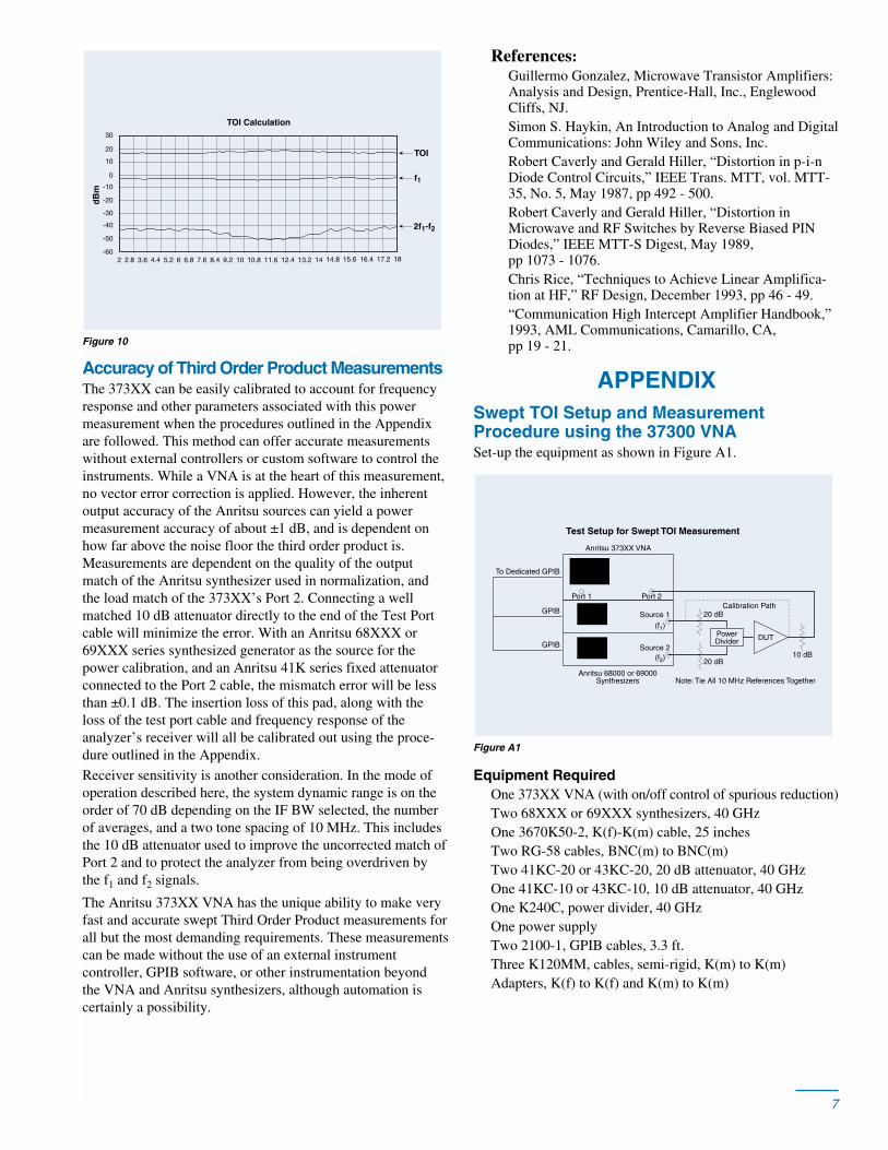
Third order product data can be taken at sufficiently highenough speed to make adjustments to the amplifier bias tooptimize performance. TOI calculations can be done quicklyand easily using an external PC, after the data is brought intoa spreadsheet program such as Excel (typical data is plottedin Figure 10).
Anritsu 373XX VNA
Anritsu Synthesizers
DUT
Intermodulation Measurements using the 373XX VNA
6
7
Figure 10
Accuracy of Third Order Product MeasurementsThe 373XX can be easily calibrated to account for frequencyresponse and other parameters associated with this powermeasurement when the procedures outlined in the Appendixare followed. This method can offer accurate measurementswithout external controllers or custom software to control theinstruments. While a VNA is at the heart of this measurement,no vector error correction is applied. However, the inherentoutput accuracy of the Anritsu sources can yield a powermeasurement accuracy of about ±1 dB, and is dependent onhow far above the noise floor the third order product is.Measurements are dependent on the quality of the outputmatch of the Anritsu synthesizer used in normalization, andthe load match of the 373XX’s Port 2. Connecting a wellmatched 10 dB attenuator directly to the end of the Test Portcable will minimize the error. With an Anritsu 68XXX or69XXX series synthesized generator as the source for thepower calibration, and an Anritsu 41K series fixed attenuatorconnected to the Port 2 cable, the mismatch error will be lessthan ±0.1 dB. The insertion loss of this pad, along with theloss of the test port cable and frequency response of theanalyzer’s receiver will all be calibrated out using the proce-dure outlined in the Appendix.
Receiver sensitivity is another consideration. In the mode ofoperation described here, the system dynamic range is on theorder of 70 dB depending on the IF BW selected, the numberof averages, and a two tone spacing of 10 MHz. This includesthe 10 dB attenuator used to improve the uncorrected match ofPort 2 and to protect the analyzer from being overdriven bythe f1 and f2 signals.
The Anritsu 373XX VNA has the unique ability to make veryfast and accurate swept Third Order Product measurements forall but the most demanding requirements. These measurementscan be made without the use of an external instrumentcontroller, GPIB software, or other instrumentation beyondthe VNA and Anritsu synthesizers, although automation iscertainly a possibility.
References:Guillermo Gonzalez, Microwave Transistor Amplifiers:Analysis and Design, Prentice-Hall, Inc., EnglewoodCliffs, NJ.Simon S. Haykin, An Introduction to Analog and DigitalCommunications: John Wiley and Sons, Inc.Robert Caverly and Gerald Hiller, “Distortion in p-i-nDiode Control Circuits,” IEEE Trans. MTT, vol. MTT-35, No. 5, May 1987, pp 492 - 500.Robert Caverly and Gerald Hiller, “Distortion inMicrowave and RF Switches by Reverse Biased PINDiodes,” IEEE MTT-S Digest, May 1989, pp 1073 - 1076.Chris Rice, “Techniques to Achieve Linear Amplifica-tion at HF,” RF Design, December 1993, pp 46 - 49.“Communication High Intercept Amplifier Handbook,”1993, AML Communications, Camarillo, CA, pp 19 - 21.
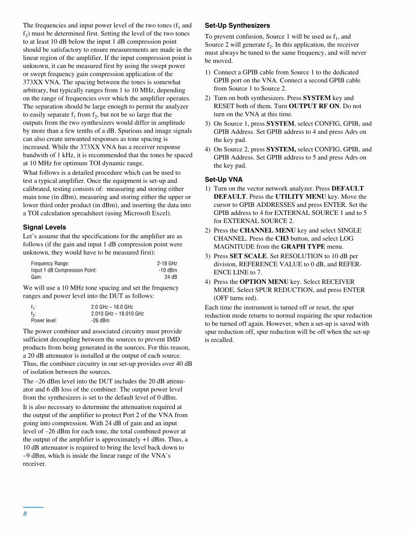
APPENDIXSwept TOI Setup and MeasurementProcedure using the 37300 VNASet-up the equipment as shown in Figure A1.
Figure A1
Equipment RequiredOne 373XX VNA (with on/off control of spurious reduction)Two 68XXX or 69XXX synthesizers, 40 GHzOne 3670K50-2, K(f)-K(m) cable, 25 inchesTwo RG-58 cables, BNC(m) to BNC(m)Two 41KC-20 or 43KC-20, 20 dB attenuator, 40 GHzOne 41KC-10 or 43KC-10, 10 dB attenuator, 40 GHzOne K240C, power divider, 40 GHzOne power supplyTwo 2100-1, GPIB cables, 3.3 ft.Three K120MM, cables, semi-rigid, K(m) to K(m)Adapters, K(f) to K(f) and K(m) to K(m)
Anritsu 373XX VNA
Anritsu 68000 or 69000Synthesizers
PowerDivider DUT
20 dB
20 dB10 dB
Port 2
Source 1
Port 1
To Dedicated GPIB
GPIB
GPIB
Calibration Path
(f2)
(f1)
Note: Tie All 10 MHz References Together
Source 2
Test Setup for Swept TOI Measurement
2 2.8 3.6 4.4 5.2 6 6.8 7.6 8.4 9.2 10 10.8 11.6 12.4 13.2 14 14.8
30
TOI Calculation
dB
m
20
10
0
-10
-20
-30
-40
-50
-60
TOI
f1
2f1-f2
15.6 16.4 17.2 18
The frequencies and input power level of the two tones (f1 andf2) must be determined first. Setting the level of the two tonesto at least 10 dB below the input 1 dB compression pointshould be satisfactory to ensure measurements are made in thelinear region of the amplifier. If the input compression point isunknown, it can be measured first by using the swept poweror swept frequency gain compression application of the373XX VNA. The spacing between the tones is somewhatarbitrary, but typically ranges from 1 to 10 MHz, dependingon the range of frequencies over which the amplifier operates.The separation should be large enough to permit the analyzerto easily separate f1 from f2, but not be so large that theoutputs from the two synthesizers would differ in amplitudeby more than a few tenths of a dB. Spurious and image signalscan also create unwanted responses as tone spacing isincreased. While the 373XX VNA has a receiver responsebandwith of 1 kHz, it is recommended that the tones be spacedat 10 MHz for optimum TOI dynamic range.
What follows is a detailed procedure which can be used totest a typical amplifier. Once the equipment is set-up andcalibrated, testing consists of: measuring and storing eithermain tone (in dBm), measuring and storing either the upper orlower third order product (in dBm), and inserting the data intoa TOI calculation spreadsheet (using Microsoft Excel).
Signal LevelsLet’s assume that the specifications for the amplifier are asfollows (if the gain and input 1 dB compression point wereunknown, they would have to be measured first):
Frequency Range: 2-18 GHzInput 1 dB Compression Point: -10 dBmGain: 24 dB
We will use a 10 MHz tone spacing and set the frequencyranges and power level into the DUT as follows:
f1: 2.0 GHz – 18.0 GHzf2: 2.010 GHz – 18.010 GHzPower level: -26 dBm
The power combiner and associated circuitry must providesufficient decoupling between the sources to prevent IMDproducts from being generated in the sources. For this reason,a 20 dB attenuator is installed at the output of each source.Thus, the combiner circuitry in our set-up provides over 40 dBof isolation between the sources.
The –26 dBm level into the DUT includes the 20 dB attenu-ator and 6 dB loss of the combiner. The output power levelfrom the synthesizers is set to the default level of 0 dBm.
It is also necessary to determine the attenuation required atthe output of the amplifier to protect Port 2 of the VNA fromgoing into compression. With 24 dB of gain and an inputlevel of –26 dBm for each tone, the total combined power atthe output of the amplifier is approximately +1 dBm. Thus, a10 dB attenuator is required to bring the level back down to–9 dBm, which is inside the linear range of the VNA’sreceiver.
Set-Up Synthesizers
To prevent confusion, Source 1 will be used as f1, andSource 2 will generate f2. In this application, the receivermust always be tuned to the same frequency, and will neverbe moved.
1) Connect a GPIB cable from Source 1 to the dedicatedGPIB port on the VNA. Connect a second GPIB cablefrom Source 1 to Source 2.
2) Turn on both synthesizers. Press SYSTEM key andRESET both of them. Turn OUTPUT RF ON. Do notturn on the VNA at this time.
3) On Source 1, press SYSTEM, select CONFIG, GPIB, andGPIB Address. Set GPIB address to 4 and press Adrs onthe key pad.
4) On Source 2, press SYSTEM, select CONFIG, GPIB, andGPIB Address. Set GPIB address to 5 and press Adrs onthe key pad.
Set-Up VNA1) Turn on the vector network analyzer. Press DEFAULT
DEFAULT. Press the UTILITY MENU key. Move thecursor to GPIB ADDRESSES and press ENTER. Set theGPIB address to 4 for EXTERNAL SOURCE 1 and to 5for EXTERNAL SOURCE 2.
2) Press the CHANNEL MENU key and select SINGLECHANNEL. Press the CH3 button, and select LOGMAGNITUDE from the GRAPH TYPE menu.
3) Press SET SCALE. Set RESOLUTION to 10 dB perdivision, REFERENCE VALUE to 0 dB, and REFER-ENCE LINE to 7.
4) Press the OPTION MENU key. Select RECEIVERMODE. Select SPUR REDUCTION, and press ENTER(OFF turns red).
Each time the instrument is turned off or reset, the spurreduction mode returns to normal requiring the spur reductionto be turned off again. However, when a set-up is saved withspur reduction off, spur reduction will be off when the set-upis recalled.
8

9
Redefine S-ParametersS-parameters are ratio (relative) measurements, and aredefined in dB. Harmonic or intermodulation products aremeasured as an absolute power level (non-ratio) in dBm.Therefore, the S-parameters must be defined as follows:
1) Press the S PARAMS key and select S21. Press 1 toREDEFINE SELECTED PARAMETER. SelectS21/USER 1. Press ENTER to switch (USER 1 turns red).
2) Select CHANGE RATIO and press ENTER. UnderNUMERATOR, select B2 (Tb), and press ENTER. UnderDENOMINATOR, select 1 (UNITY) and press ENTER.Top left of screen should display B2/1.
The analyzer is now configured to measure power, but is notyet calibrated to read in dBm.
Set-Up Multiple Source Control
The frequency for f1, f2, and the receive frequency for theVNA are entered through the MULTIPLE SOURCECONTROL menu.
1) Press the OPTION MENU key, select MULTIPLESOURCE CONTROL, and then DEFINE BANDS. SetBAND START FREQ to 2.0 GHz and set BAND STOPFREQ to 18.0 GHz. Band start and band stop frequenciesbecome the “X” axis of the display. All directly controlledsources and receive frequencies are referenced to F, as Fsweeps from band start to band stop.
2) Select EDIT SYSTEM EQUATIONS. Select SOURCE 2and change OFFSET FREQ to 0.010 GHz. This will offsetSource 2 by +10 MHz from Source 1. The systemequations should now read as follows:
SOURCE 1 = (1/1) * (F + 0.000 GHz)�
SOURCE 2 = (1/1) * (F + 0.010 GHz)➁
RECEIVER = (1/1) * (F + 0.000 GHz)➂
After verifying the above equations, select PREVIOUSMENU then STORE BAND 1. If an OUT OF RANGEerror message occurs at any point in this procedure,then the band 1 start and stop frequencies must be re-entered. Any system equation that results in a frequencywhich falls outside the frequency range of the synthesizersor receive range of the analyzer will result in an out ofrange by formula error.
3) Select SET MULTIPLE SOURCE MODE, then select ONto set Source 1 (f1) and Source 2 (f2). At this point Source 1is sweeping over the specified f1 range. The Receiver isalso tuned to f1 by formula. Source 2 (f2) is sweeping witha +10 MHz offset from f1.
Perform Power CalibrationAs mentioned earlier, these measurements are absolute power,and non-ratio measurements, therefore normal VNA calibra-tion techniques do not apply. The 373XX is normalized forpower measurements by taking advantage of the inherentpower flatness of Anritsu synthesizers. The following stepseffectively transfer this accuracy to the VNA:
1) Select a Port 2 test cable which is long enough to reachboth the DUT and the output connector of the Source 1synthesizer. As shown in the equipment set-up diagram,connect a well matched 10 dB attenuator to the Port 2 testport cable, improving its match. It must be included duringboth calibration and measurement. This power calibrationcorrects for frequency flatness of the receiver, the test portcable, and any additional internal or external attenuators.If the 10 dB attenuator is insufficient to reduce the DUToutput power at f1 and f2 to within the linear range of theVNA, then add additional internal step attenuation at Port 2to prevent the analyzer from going into compression.
2) Connect the Port 2 test cable and attenuator to Source 1 asshown in Figure A1 (calibration path). Press DATAPOINTS and set to 101 points. Press AVG/SMOOTHMENU and set AVERAGING to 100 measurements perpoint. Press AVERAGE to turn on averaging. PressVIDEO IF BW and set to 100 Hz. After one sweep hasbeen completed and the display is stabilized, pressTRACE MEMORY and select STORE DATA TOMEMORY. Then select VIEW DATA (/) BY MEMORY.Since this is not a built-in calibration procedure, the cali-bration light does not activate. Trace memory can also bestored to the hard disk or floppy disk for future recall.
The display is now normalized to 0 dBm (output of Source 1).This method should provide a power measuring accuracyapproximately equal to the level accuracy of the synthesizerplus any mismatch error. Level accuracy of the specifiedsources is ±0.1 dB at 0 dBm output. If a precision attenuatoris used on the Port 2 cable, then this mismatch error will beless than ±0.1 dB.
Before making measurements it is a good idea to check theVNA control of the synthesizers. To do this press SETUPMENU, select TEST SIGNALS, and change SOURCE 1PWR to –50 dBm. Repeat for Source 2. Observe the leveland flatness of the trace.
It is important that all measurements be made at the exactfrequencies at which normalization/calibration was performed.If the number of data points must be changed, trace memorywill be turned off, thus voiding the calibration. If this is doneaccidentally, return the data points to the original numberand activate trace memory again. The markers and limit lineswill readout in dB. Since the power calibration above wasreferenced to 0 dBm, then 0 dB is equal to 0 dBm.
� Source 1 (f1) sweeps from 2 to 18 GHz.➁ Source 2 (f2) sweeps from 2.010 to 18.010 GHz➂ The Receiver is set to receive from 2 to 18 GHz
Measure and Store Output Power (f1)
Without changing Source 1, Source 2, or the Receiverfrequencies, the system is set to measure f1 power in dBm.In order to calculate the output TOI point from the third orderproducts, the output power of one tone (f1 in this case) mustalso be measured and stored to a floppy disk.
1) Remove the Port 2 test cable (with 10 dB attenuatorattached) from Source 1 and connect it to the DUT outputas shown in Figure A1. Reconnect Source 1 to the powerdivider (with the 20 dB attenuator in series). Apply DCpower to the DUT.
2) Press the MENU key in the HARD COPY key group.Press DISK FILE and then under DISK FILE OPTIONS,select FLOPPY DISK and TEXT. Press the STARTPRINT key. Press ENTER (to clear the previous filename), and then enter the letters “F1,” and select DONE.The file is stored as a DOS compatible, text file. Threecolumns of data are stored: the data point number, thefrequency and the amplitude.
It may be desirable to also measure f2 to verify level balance.The multiple source equations must be modified as followsand the data stored on a floppy disk.
SOURCE 1 = (1/1) * (F - 0.010 GHz)➃
SOURCE 2 = (1/1) * (F + 0.000 GHz)RECEIVER = (1/1) * (F + 0.000 GHz)
In this way, the VNA can display the swept power of f1, f2,2f1 - f2 or 2f2 - f1, depending on where Source 1 and 2 aretuned. While it is more intuitive to move the receiverfrequency, the calibration is only valid when the analyzerreceives the frequencies at which it was calibrated. For thisreason the receiver frequency is never changed throughoutthis procedure, and only Source 1 and 2 are shifted withrespect to the receiver.
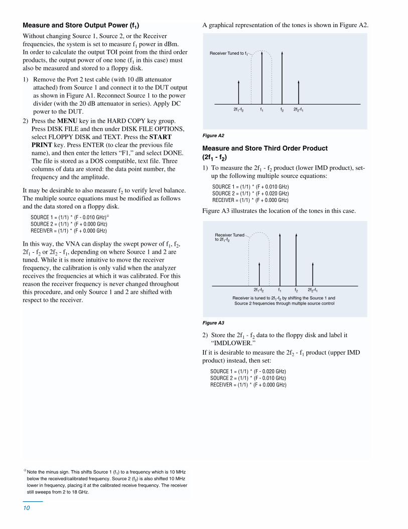
A graphical representation of the tones is shown in Figure A2.
Figure A2
Measure and Store Third Order Product (2f1 - f2)
1) To measure the 2f1 - f2 product (lower IMD product), set-up the following multiple source equations:
SOURCE 1 = (1/1) * (F + 0.010 GHz)SOURCE 2 = (1/1) * (F + 0.020 GHz)RECEIVER = (1/1) * (F + 0.000 GHz)
Figure A3 illustrates the location of the tones in this case.
Figure A3
2) Store the 2f1 - f2 data to the floppy disk and label it“IMDLOWER.”
If it is desirable to measure the 2f2 - f1 product (upper IMDproduct) instead, then set:
SOURCE 1 = (1/1) * (F - 0.020 GHz)SOURCE 2 = (1/1) * (F - 0.010 GHz)RECEIVER = (1/1) * (F + 0.000 GHz)
2f1-f2 2f2-f1f1 f2
Receiver Tuned to 2f1-f2
Receiver is tuned to 2f1-f2 by shifting the Source 1 and Source 2 frequencies through multiple source control
2f1-f2 2f2-f1f1 f2
Receiver Tuned to f1
10
➃ Note the minus sign. This shifts Source 1 (f1) to a frequency which is 10 MHzbelow the received/calibrated frequency. Source 2 (f2) is also shifted 10 MHzlower in frequency, placing it at the calibrated receive frequency. The receiverstill sweeps from 2 to 18 GHz.
11
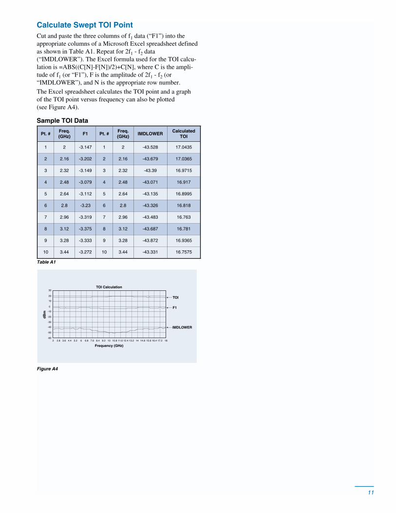
Calculate Swept TOI PointCut and paste the three columns of f1 data (“F1”) into theappropriate columns of a Microsoft Excel spreadsheet definedas shown in Table A1. Repeat for 2f1 - f2 data(“IMDLOWER”). The Excel formula used for the TOI calcu-lation is =ABS((C[N]-F[N])/2)+C[N], where C is the ampli-tude of f1 (or “F1”), F is the amplitude of 2f1 - f2 (or“IMDLOWER”), and N is the appropriate row number.
The Excel spreadsheet calculates the TOI point and a graphof the TOI point versus frequency can also be plotted(see Figure A4).
Sample TOI Data
Table A1
Figure A4
30TOI Calculation
Frequency (GHz)
dB
m
20
10
0
-10
-20
-30
-40
-50
-60
TOI
F1
IMDLOWER
2 2.8 3.6 4.4 5.2 6 6.8 7.6 8.4 9.2 10 10.8 11.6 12.4 13.2 14 14.8 15.6 16.4 17.2 18
Pt. #Freq.(GHz)
F1 Pt. #Freq. (GHz)
IMDLOWER Calculated
TOI
1 2 -3.147 1 2 -43.528 17.0435
2 2.16 -3.202 2 2.16 -43.679 17.0365
3 2.32 -3.149 3 2.32 -43.39 16.9715
4 2.48 -3.079 4 2.48 -43.071 16.917
5 2.64 -3.112 5 2.64 -43.135 16.8995
6 2.8 -3.23 6 2.8 -43.326 16.818
7 2.96 -3.319 7 2.96 -43.483 16.763
8 3.12 -3.375 8 3.12 -43.687 16.781
9 3.28 -3.333 9 3.28 -43.872 16.9365
10 3.44 -3.272 10 3.44 -43.331 16.7575

September 2000, Rev. A 11410-00257Data subject to change without notice Intermodulation Distortion Measurements Using the 37300 Series Vector Network Analyzer Application Note/GIP-G
All trademarks are registered trademarks of their respective companies.
Microwave Measurements Division • 490 Jarvis Drive • Morgan Hill, CA 95037-2809http://www.us.anritsu.com • FAX (408) 778-0239
Sales Centers:United States (800) ANRITSUCanada (800) ANRITSUSouth America 55 (21) 286-9141
Sales Centers:Europe 44 (01582) 433200Japan 81 (03) 3446-1111Asia-Pacific 65-2822400


