

FN7707Rev 5.00
October 13, 2016
ISL89163, ISL89164, ISL89165High Speed, Dual Channel, 6A, Power MOSFET Driver with Enable Inputs
DATASHEET
The ISL89163, ISL89164, and ISL89165 are high-speed, 6A, dual channel MOSFET drivers with enable inputs. These parts are very similar to the ISL89160, ISL89161, ISL89162 drivers but with an added enable input for each channel occupying NC pins 1 and 8 of the ISL89160, ISL89161, ISL89162.
Precision thresholds on all logic inputs allow the use of external RC circuits to generate accurate and stable time delays on both the main channel inputs, INA and INB, and the enable inputs, ENA and ENB. The precision delays capable of these precise logic thresholds makes these parts very useful for dead-time control and synchronous rectifiers. Note that the ENable and INput logic inputs can be interchanged for alternate logic implementations.
Three input logic thresholds are available: 3.3V (CMOS), 5.0V (CMOS or TTL compatible), and CMOS thresholds that are proportional to VDD.
At high switching frequencies, these MOSFET drivers use very little internal bias currents. Separate, non-overlapping drive circuits are used to drive each CMOS output FET to prevent shoot-through currents in the output stage.
The start-up sequence is designed to prevent unexpected glitches when VDD is being turned on or turned off. When VDD < ~1V, an internal 10kΩ resistor between the output and ground helps to keep the output voltage low. When ~1V < VDD < UV, both outputs are driven low with very low resistance and the logic inputs are ignored. This insures that the driven FETs are off. When VDD > UVLO, and after a short delay, the outputs now respond to the logic inputs.
Features• Dual output, 6A peak currents, can be paralleled
• Dual AND-ed input logic, (INput and ENable)
• Typical ON-resistance <1Ω
• Specified Miller plateau drive currents
• Very low thermal impedance (JC = 3°C/W)
• Hysteretic Input logic levels for 3.3V CMOS, 5V CMOS, TTL, and Logic levels proportional to VDD
• Precision threshold inputs for time delays with external RC components
• 20ns rise and fall time driving a 10nF load.
Applications• Synchronous Rectifier (SR) driver
• Switch mode power supplies
• Motor drives, Class D amplifiers, UPS, inverters
• Pulse transformer driver
• Clock/line driver
Related Literature• For a full list of related documents, visit our web page
• ISL89163, ISL89164, ISL89165 product pages
FIGURE 1. TYPICAL APPLICATION FIGURE 2. TEMP STABLE LOGIC THRESHOLDS
8
6
7
1
4
3
2
5
EPAD
VDD
4.7µF
ENBENA
INA
INB
GND
OUTA
OUTB
0.0
0.5
1.0
1.5
2.0
2.5
3.0
-40 -25 -10 5 20 35 50 65 80 95 110 125
OP
TIO
N B
TH
RE
SH
OL
DS
(5.
0V
)
TEMPERATURE (°C)
NEGATIVE THRESHOLD LIMITS
POSITIVE THRESHOLD LIMITS
FN7707 Rev 5.00 Page 1 of 16October 13, 2016

ISL89163, ISL89164, ISL89165
Block Diagram
OUTx
VDD
INx
GND
FOR CLARITY, ONLY ONE CHANNEL IS SHOWN
EPAD
FOR PROPER THERMAL AND ELECTRICAL PERFORMANCE, THE EPAD MUST BE
CONNECTED TO THE PCB GROUND PLANE.
SEPARATE FET DRIVES, WITH NON-OVERLAPPING OUTPUTS, PREVENT
SHOOT-THRU CURRENTS IN THE OUTPUT CMOS FETS RESULTING WITH VERY LOW
HIGH FREQUENCY OPERATING CURRENTS.
ISL89164, ISL89165
ISL89163
10k
ENx
ENX AND INX INPUTS ARE IDENTICAL AND MAY BE
INTERCHANGED FOR ALTERNATE LOGIC
FOR OPTIONS A AND B, THE UV COMPARATOR HOLDS OFF THE OUTPUTS UNTIL VDD ~> 3.3VDC.
FOR OPTION C, THE UV RELEASE IS ~> 6.5V
FIGURE 3. BLOCK DIAGRAM
Pin ConfigurationsISL89163FR, ISL89163FB
(8 LD TDFN, EPSOIC)TOP VIEW
ISL89164FR, ISL89164FB(8 LD TDFN, EPSOIC)
TOP VIEW
ISL89165FR, ISL89165FB(8 LD TDFN, EPSOIC)
TOP VIEW
1ENA
2INA
4INB
3GND
8 ENB
7 OUTA
6 VDD
5 OUTB
1ENA
2/INA
4/INB
3GND
8 ENB
7 OUTA
6 VDD
5 OUTB
1ENA
2/INA
4INB
3GND
8 ENB
7 OUTA
6 VDD
5 OUTB
Pin Descriptions
PIN NUMBER SYMBOL
DESCRIPTION(SEE TRUTH TABLE FOR
LOGIC POLARITIES)
1 ENA Channel A enable, 0V to VDD
2 INA, /INA Channel A input, 0V to VDD
3 GND Power Ground, 0V
4 INB, /INB Channel B enable, 0V to VDD
5 OUTB Channel B output
6 VDD Power input, 4.5V to 16V
7 OUTA Channel A output, 0V to VDD
8 ENB Channel B enable, 0V to VDD
EPAD Power Ground, 0V
0 0 0
0 1 0
1 0 0
1 1 0
OUTxENx
/INx
x x 0
OUTxENx
INx
*SUBSTITUTE A OR B FOR x
NON-INVERTING INVERTING
ENx* /INx* OUTx*ENx* INx* OUTx*
0
0
0
0
0 0 0
0 1 0
1 0 1
1 1 0
1
1
1
1
UV
0
1
1
1
1
UV
0 0 0
0 1 0
1 0 0
1 1 1
0 1 0
1 0 0
1 1 0
0
0
0
FN7707 Rev 5.00 Page 2 of 16October 13, 2016
ISL89163, ISL89164, ISL89165
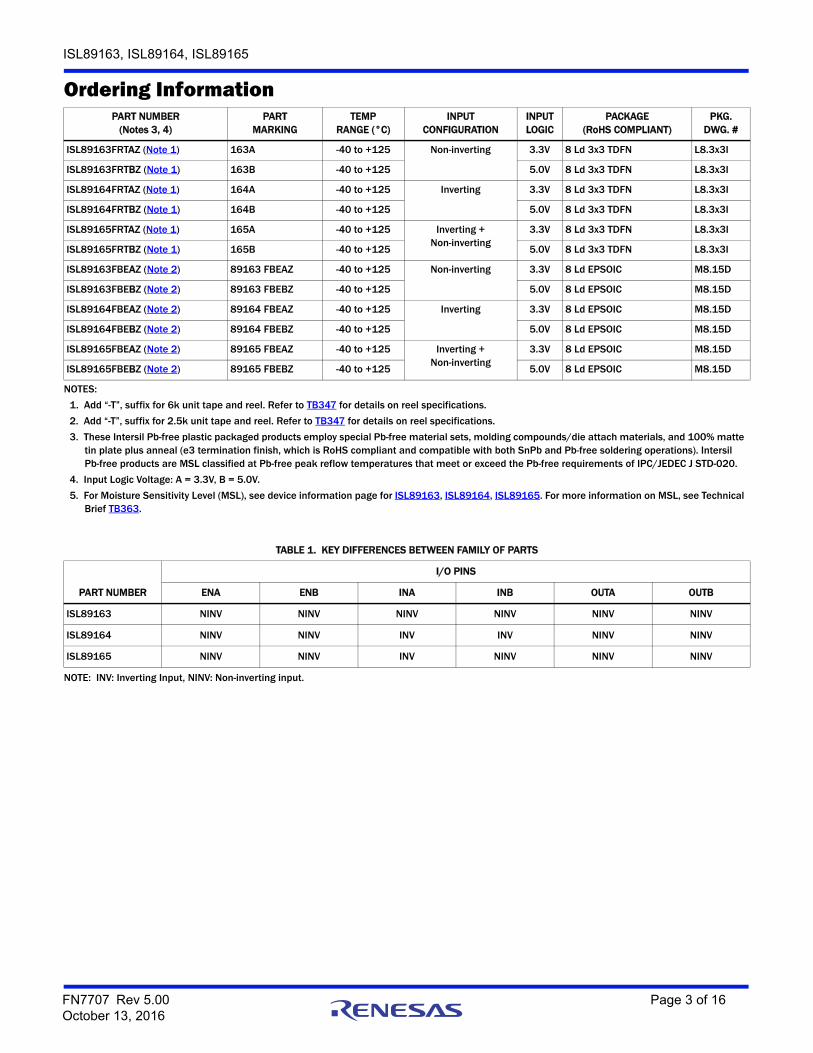
Ordering InformationPART NUMBER
(Notes 3, 4)PART
MARKINGTEMP
RANGE (°C)INPUT
CONFIGURATIONINPUTLOGIC
PACKAGE(RoHS COMPLIANT)
PKG.DWG. #
ISL89163FRTAZ (Note 1) 163A -40 to +125 Non-inverting 3.3V 8 Ld 3x3 TDFN L8.3x3I
ISL89163FRTBZ (Note 1) 163B -40 to +125 5.0V 8 Ld 3x3 TDFN L8.3x3I
ISL89164FRTAZ (Note 1) 164A -40 to +125 Inverting 3.3V 8 Ld 3x3 TDFN L8.3x3I
ISL89164FRTBZ (Note 1) 164B -40 to +125 5.0V 8 Ld 3x3 TDFN L8.3x3I
ISL89165FRTAZ (Note 1) 165A -40 to +125 Inverting +Non-inverting
3.3V 8 Ld 3x3 TDFN L8.3x3I
ISL89165FRTBZ (Note 1) 165B -40 to +125 5.0V 8 Ld 3x3 TDFN L8.3x3I
ISL89163FBEAZ (Note 2) 89163 FBEAZ -40 to +125 Non-inverting 3.3V 8 Ld EPSOIC M8.15D
ISL89163FBEBZ (Note 2) 89163 FBEBZ -40 to +125 5.0V 8 Ld EPSOIC M8.15D
ISL89164FBEAZ (Note 2) 89164 FBEAZ -40 to +125 Inverting 3.3V 8 Ld EPSOIC M8.15D
ISL89164FBEBZ (Note 2) 89164 FBEBZ -40 to +125 5.0V 8 Ld EPSOIC M8.15D
ISL89165FBEAZ (Note 2) 89165 FBEAZ -40 to +125 Inverting +Non-inverting
3.3V 8 Ld EPSOIC M8.15D
ISL89165FBEBZ (Note 2) 89165 FBEBZ -40 to +125 5.0V 8 Ld EPSOIC M8.15D
NOTES:
1. Add “-T”, suffix for 6k unit tape and reel. Refer to TB347 for details on reel specifications.
2. Add “-T”, suffix for 2.5k unit tape and reel. Refer to TB347 for details on reel specifications.
3. These Intersil Pb-free plastic packaged products employ special Pb-free material sets, molding compounds/die attach materials, and 100% matte tin plate plus anneal (e3 termination finish, which is RoHS compliant and compatible with both SnPb and Pb-free soldering operations). Intersil Pb-free products are MSL classified at Pb-free peak reflow temperatures that meet or exceed the Pb-free requirements of IPC/JEDEC J STD-020.
4. Input Logic Voltage: A = 3.3V, B = 5.0V.
5. For Moisture Sensitivity Level (MSL), see device information page for ISL89163, ISL89164, ISL89165. For more information on MSL, see Technical Brief TB363.
TABLE 1. KEY DIFFERENCES BETWEEN FAMILY OF PARTS
PART NUMBER
I/O PINS
ENA ENB INA INB OUTA OUTB
ISL89163 NINV NINV NINV NINV NINV NINV
ISL89164 NINV NINV INV INV NINV NINV
ISL89165 NINV NINV INV NINV NINV NINV
NOTE: INV: Inverting Input, NINV: Non-inverting input.
FN7707 Rev 5.00 Page 3 of 16October 13, 2016
ISL89163, ISL89164, ISL89165
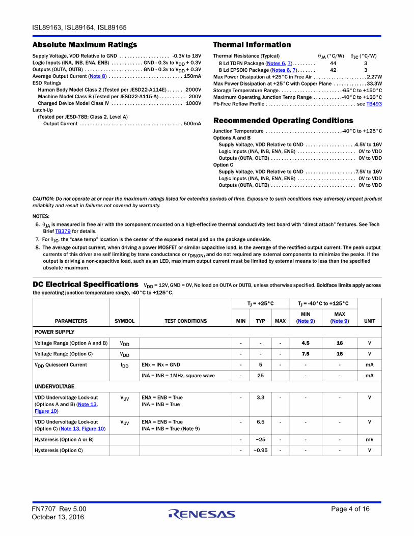
Absolute Maximum Ratings Thermal InformationSupply Voltage, VDD Relative to GND . . . . . . . . . . . . . . . . . . . -0.3V to 18VLogic Inputs (INA, INB, ENA, ENB) . . . . . . . . . . . . GND - 0.3v to VDD + 0.3VOutputs (OUTA, OUTB) . . . . . . . . . . . . . . . . . . . . . . GND - 0.3v to VDD + 0.3VAverage Output Current (Note 8) . . . . . . . . . . . . . . . . . . . . . . . . . . . . 150mAESD Ratings
Human Body Model Class 2 (Tested per JESD22-A114E) . . . . . . 2000VMachine Model Class B (Tested per JESD22-A115-A) . . . . . . . . . . 200VCharged Device Model Class IV . . . . . . . . . . . . . . . . . . . . . . . . . . . 1000V
Latch-Up(Tested per JESD-78B; Class 2, Level A)
Output Current . . . . . . . . . . . . . . . . . . . . . . . . . . . . . . . . . . . . . . . 500mA
Thermal Resistance (Typical) JA (°C/W) JC (°C/W)8 Ld TDFN Package (Notes 6, 7). . . . . . . . . 44 38 Ld EPSOIC Package (Notes 6, 7) . . . . . . . 42 3
Max Power Dissipation at +25°C in Free Air . . . . . . . . . . . . . . . . . . . . . 2.27WMax Power Dissipation at +25°C with Copper Plane . . . . . . . . . . . . .33.3WStorage Temperature Range. . . . . . . . . . . . . . . . . . . . . . . .-65°C to +150°CMaximum Operating Junction Temp Range . . . . . . . . . . .-40°C to +150°CPb-Free Reflow Profile . . . . . . . . . . . . . . . . . . . . . . . . . . . . . . . . . . see TB493
Recommended Operating ConditionsJunction Temperature . . . . . . . . . . . . . . . . . . . . . . . . . . . . .-40°C to +125°COptions A and B
Supply Voltage, VDD Relative to GND . . . . . . . . . . . . . . . . . . .4.5V to 16VLogic Inputs (INA, INB, ENA, ENB) . . . . . . . . . . . . . . . . . . . . . . 0V to VDDOutputs (OUTA, OUTB) . . . . . . . . . . . . . . . . . . . . . . . . . . . . . . . . 0V to VDD
Option CSupply Voltage, VDD Relative to GND . . . . . . . . . . . . . . . . . . .7.5V to 16VLogic Inputs (INA, INB, ENA, ENB) . . . . . . . . . . . . . . . . . . . . . . 0V to VDDOutputs (OUTA, OUTB) . . . . . . . . . . . . . . . . . . . . . . . . . . . . . . . . 0V to VDD
CAUTION: Do not operate at or near the maximum ratings listed for extended periods of time. Exposure to such conditions may adversely impact productreliability and result in failures not covered by warranty.
NOTES:
6. JA is measured in free air with the component mounted on a high-effective thermal conductivity test board with “direct attach” features. See Tech Brief TB379 for details.
7. For JC, the “case temp” location is the center of the exposed metal pad on the package underside.
8. The average output current, when driving a power MOSFET or similar capacitive load, is the average of the rectified output current. The peak output currents of this driver are self limiting by trans conductance or rDS(ON) and do not required any external components to minimize the peaks. If the output is driving a non-capacitive load, such as an LED, maximum output current must be limited by external means to less than the specified absolute maximum.
DC Electrical Specifications VDD = 12V, GND = 0V, No load on OUTA or OUTB, unless otherwise specified. Boldface limits apply across the operating junction temperature range, -40°C to +125°C.
PARAMETERS SYMBOL TEST CONDITIONS
TJ = +25°C TJ = -40°C to +125°C
UNITMIN TYP MAXMIN
(Note 9)MAX
(Note 9)
POWER SUPPLY
Voltage Range (Option A and B) VDD - - - 4.5 16 V
Voltage Range (Option C) VDD - - - 7.5 16 V
VDD Quiescent Current IDD ENx = INx = GND - 5 - - - mA
INA = INB = 1MHz, square wave - 25 - - mA
UNDERVOLTAGE
VDD Undervoltage Lock-out (Options A and B) (Note 13, Figure 10)
VUV ENA = ENB = TrueINA = INB = True
- 3.3 - - - V
VDD Undervoltage Lock-out (Option C) (Note 13, Figure 10)
VUV ENA = ENB = TrueINA = INB = True (Note 9)
- 6.5 - - - V
Hysteresis (Option A or B) - ~25 - - - mV
Hysteresis (Option C) - ~0.95 - - - V
FN7707 Rev 5.00 Page 4 of 16October 13, 2016

ISL89163, ISL89164, ISL89165
INPUTS
Input Range for INA, INB, ENA, ENB
VIN Option A, B, or C - - -GND VDD
V
Logic 0 Thresholdfor INA, INB, ENA, ENB(Note 12)
VIL Option A, nominally 37% x 3.3V - 1.22 - 1.12 1.32 V
Option B, nominally 37% x 5.0V - 1.85 - 1.70 2.00 V
Option C, nominally 20% x 12V (Note 10)
- 2.4 - 2.00 2.76 V
Logic 1 Threshold for INA, INB, ENA, ENB(Note 12)
VIH Option A, nominally 63% x 3.3V - 2.08 - 1.98 2.18 V
Option B, nominally 63% x 5.0V - 3.15 - 3.00 3.30 V
Option C, nominally 80% x 12V (Note 10)
- 9.6 - 9.24 9.96 V
Input Capacitance of INA, INB, ENA, ENB (Note 11)
CIN - 2 - - - pF
Input Bias Currentfor INA, INB, ENA, ENB
IIN GND < VIN < VDD - - - -10 +10 µA
OUTPUTS
High Level Output Voltage VOHA VOHB - - - VDD - 0.1 VDD V
Low Level Output Voltage VOLAVOLB
- - - GND GND + 0.1 V
Peak Output Source Current IO VO (initial) = 0V, CLOAD = 10nF - -6 - - - A
Peak Output Sink Current IO VO (initial) = 12V, CLOAD = 10nF - +6 - - - A
NOTES:
9. Parameters with MIN and/or MAX limits are 100% tested at +25°C, unless otherwise specified. Temperature limits established by characterization and are not production tested.
10. The nominal 20% and 80% thresholds for option C are valid for any value within the specified range of VDD.
11. This parameter is taken from the simulation models for the input FET. The actual capacitance on this input will be dominated by the PCB parasitic capacitance.
12. The true state input voltage for the non-inverted inputs is greater than the Logic 1 threshold voltage. The true state input voltage for the inverted inputs is less than the logic 0 threshold voltage.
13. A 400µs delay further inhibits the release of the output state when the UV positive going threshold is crossed. See Figure 10 on page 8.
DC Electrical Specifications VDD = 12V, GND = 0V, No load on OUTA or OUTB, unless otherwise specified. Boldface limits apply across the operating junction temperature range, -40°C to +125°C. (Continued)
PARAMETERS SYMBOL TEST CONDITIONS
TJ = +25°C TJ = -40°C to +125°C
UNITMIN TYP MAXMIN
(Note 9)MAX
(Note 9)
FN7707 Rev 5.00 Page 5 of 16October 13, 2016

ISL89163, ISL89164, ISL89165
AC Electrical Specifications VDD = 12V, GND = 0V, No Load on OUTA or OUTB, unless otherwise specified. Boldface limits apply over the operating junction temperature range, -40°C to +125°C.
PARAMETERS SYMBOL TEST CONDITIONS /NOTES
TJ = +25°C TJ = -40°C to +125°C
UNITMIN TYP MAX MIN MAX
Output Rise Time (see Figure 5) tR CLOAD = 10nF,10% to 90%
- 20 - - 40 ns
Output Fall Time (see Figure 5) tF CLOAD = 10nF, 90% to 10% - 20 - - 40 ns
Output Rising Edge Propagation Delay for Non-Inverting Inputs (Note 14)(see Figure 4)
tRDLYn VDD = 12VOptions A and B
- 25 - - 50 ns
VDD = 8VOption C
- 25 - - 50 ns
Output Rising Edge Propagation Delay with Inverting Inputs (Note 14)(see Figure 4)
tRDLYi VDD = 12VOptions A and B
- 25 - - 50 ns
VDD = 8VOption C
- 25 - - 50 ns
Output Falling Edge Propagation Delay with Non-Inverting Inputs (Note 14)(see Figure 4)
tFDLYn VDD = 12VOptions A and B
- 25 - - 50 ns
VDD = 8VOption C
- 25 - - 50 ns
Output Falling Edge Propagation Delay with Inverting Inputs (Note 14)(see Figure 4)
tFDLYi VDD = 12VOptions A and B
- 25 - - 50 ns
VDD = 8VOption C
- 25 - - 50 ns
Rising Propagation Matching (see Figure 4) tRM No load - <1 - - - ns
Falling Propagation Matching (see Figure 4) tFM No load - <1 - - - ns
Miller Plateau Sink Current(See Test Circuit Figure 6)
-IMP VDD = 10V,VMILLER = 5V
- 6 - - - A
-IMP VDD = 10V, VMILLER = 3V - 4.7 - - - A
-IMP VDD = 10V, VMILLER= 2V - 3.7 - - - A
Miller Plateau Source Current(See Test Circuit Figure 7)
IMP VDD = 10V, VMILLER = 5V - 5.2 - - - A
IMP VDD = 10V, VMILLER = 3V - 5.8 - - - A
IMP VDD = 10V, VMILLER = 2V - 6.9 - - - A
Turn On Delay (Note 13, Figure 10)
Ton_delay see Figure 10 400 µs
NOTE:14. Propagation delays for option C are typically the same for the recommended operating range (7.5V ≤ VDD ≤ 16V).
FN7707 Rev 5.00 Page 6 of 16October 13, 2016

ISL89163, ISL89164, ISL89165
Test Waveforms and Circuits
FIGURE 4. PROP DELAYS AND MATCHING FIGURE 5. RISE/FALL TIMES
FIGURE 6. MILLER PLATEAU SINK CURRENT TEST CIRCUIT FIGURE 7. MILLER PLATEAU SOURCE CURRENT TEST CIRCUIT
FIGURE 8. MILLER PLATEAU SINK CURRENT FIGURE 9. MILLER PLATEAU SOURCE CURRENT
INA, INB,ENA, ENB
OUTA
OUTB
0V
3.3V Option A5.0V Option B
tRDLY
tRDLY
50% 50%
tFDLY
tFDLY
LOGIC LEVELS: OPTION A = 3.3V, OPTION B = 5.0V, OPTION C = VDD
tRM tFM
/OUTB
/OUTA
INA, INB,ENA, ENB
0V
VDD80%
20%Option C
Option A or B
OUTA OR
OUTBtR tF
90%
10%
VMILLER
10V
+ISENSE
-ISENSE
10µF
0.1µF
50m
200ns
10k
ISL8916x
10nF
VMILLER
10V
+ISENSE
-ISENSE
10µF
0.1µF
50m
200ns
10k
ISL8916x
10nF
200ns
VMILLER
-IMP
VOUT
CURRENT THROUGH 0.1
RESISTOR
10V
0A
0V
200ns
VMILLER
IMP
VOUT
CURRENT THROUGH 0.1
RESISTOR
0
FN7707 Rev 5.00 Page 7 of 16October 13, 2016
ISL89163, ISL89164, ISL89165
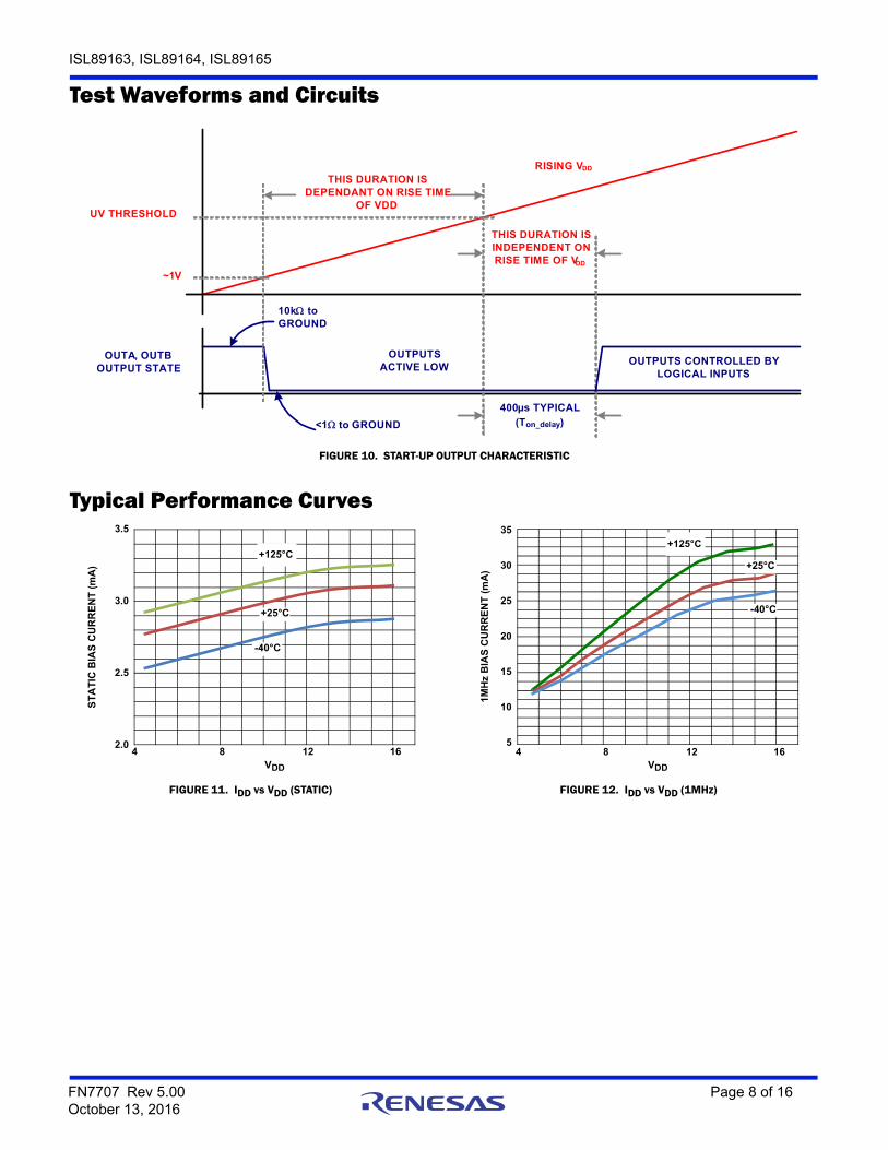
FIGURE 10. START-UP OUTPUT CHARACTERISTIC
Test Waveforms and Circuits
UV THRESHOLD
~1V
400µs TYPICAL
(Ton_delay)
OUTA, OUTBOUTPUT STATE
OUTPUTS CONTROLLED BY LOGICAL INPUTS
10k to GROUND
OUTPUTS ACTIVE LOW
<1 to GROUND
RISING VDD
THIS DURATION IS DEPENDANT ON RISE TIME
OF VDD
THIS DURATION IS INDEPENDENT ON RISE TIME OF VDD
Typical Performance Curves
FIGURE 11. IDD vs VDD (STATIC) FIGURE 12. IDD vs VDD (1MHz)
2.0
2.5
3.0
3.5
4 8 12 16
ST
AT
IC B
IAS
CU
RR
EN
T (
mA
)
VDD
+125°C
+25°C
-40°C
+125°C
+25°C
-40°C
20
25
30
35
15
10
54 8 12 16
1M
Hz
BIA
S C
UR
RE
NT
(m
A)
VDD
FN7707 Rev 5.00 Page 8 of 16October 13, 2016

ISL89163, ISL89164, ISL89165
FIGURE 13. IDD vs FREQUENCY (+25°C) FIGURE 14. rDS(ON) vs TEMPERATURE
FIGURE 15. OPTION A THRESHOLDS FIGURE 16. OPTION B THRESHOLDS
FIGURE 17. OUTPUT RISE/FALL TIME FIGURE 18. PROPAGATION DELAY vs VDD
Typical Performance Curves (Continued)
50
40
30
20
10
00 0.2 0.4 0.6 0.8 1.0 1.2 1.6 2.0
FREQUENCY (MHz)
I DD
(m
A)
NO LOAD
5V
10V
16V
12V
1.81.40.5
0.6
0.7
0.8
0.9
1.0
1.1
-45 -20 5 30 55 80 105 130
r DS
(ON
) (Ω
)
TEMPERATURE (°C)
VOUT LOW
VOUT HIGH
0.0
0.5
1.0
1.5
2.0
2.5
3.0
-45 -20 5 30 55 80 105 130
INP
UT
LO
GIC
TH
RE
SH
OL
DS
(3
.3V
)
TEMPERATURE (°C)
POSITIVE THRESHOLD
NEGATIVE THRESHOLD
3.5
0.0
0.5
1.0
1.5
2.0
2.5
3.0
-45 -20 5 30 55 80 105 130
INP
UT
LO
GIC
TH
RE
SH
OL
DS
(3.
3V
)
TEMPERATURE (°C)
POSITIVE THRESHOLD
NEGATIVE THRESHOLD
3.5
15
20
25
-45 -20 5 30 55 80 105 130
RIS
E/F
AL
L T
IME
(n
s)
TEMPERATURE (°C)
FALL TIME, CLOAD = 10nF
RISE TIME, CLOAD = 10nF
15
20
25
30
5 7 9 11 13 15
PR
OP
AG
AT
ION
DE
LA
Y (
ns)
VDD
OUTPUT FALLING PROP DELAY
OUTPUT RISING PROP DELAY
FN7707 Rev 5.00 Page 9 of 16October 13, 2016

ISL89163, ISL89164, ISL89165
Functional DescriptionOverviewThe ISL89163, ISL89164, ISL89165 MOSFET drivers incorporate several features optimized for Synchronous Rectifier (SR) driver applications including precision input logic thresholds, enable inputs, undervoltage lockout, and high amplitude output drive currents.
The precision input thresholds facilitate the use of an external RC network to delay the rising or falling propagation of the driver output. This is a useful feature for adjusting when the SRs turn on relative to the primary side FETs. In a similar manner, these drivers can also be used to control the turn-on/off timing of the primary side FETs.
The Enable inputs (ENA, ENB) are used to emulate diode operation of the SRs by disabling the driver output when it is necessary to prevent negative currents in the output filter inductors. An example is turning off the SRs when the power supply output is turned off. This prevents the output capacitor from being discharged through the output inductor. If this is allowed to happen, the voltage across the output capacitor will ring negative possibly damaging the capacitor (if it is polarized) and probably damaging the load. Another example is preventing circulating currents between paralleled power supplies during no or light load conditions. During light load conditions (especially when active load sharing is not active), energy will be transferred from the paralleled power supply that has a higher voltage to the paralleled power supply with the lower voltage. Consequently, the energy that is absorbed by the low voltage output is then transferred to the primary side causing the bus voltage to increase until the primary side is damaged by excessive voltage.
The start-up sequence for input threshold Options A, B, and C is designed to prevent unexpected glitches when VDD is being turned on or turned off. When VDD < ~1V, an internal 10kΩ resistor connected between the output and ground, help to keep the gate voltage close to ground. When ~1V < VDD < UV, both outputs are driven low while ignoring the logic inputs. This low state has the same current sinking capacity as during normal operation. This insures that the driven FETs are held off even if there is a switching voltage on the drains that can inject charge into the gates via the Miller capacitance. When VDD > UVLO, and after a 400µs delay, the outputs now respond to the logic inputs. See Figure 10 for complete details.
For the negative transition of VDD through the UV lockout voltage, the outputs of input threshold Options A or B are active low when VDD < ~3.2VDC regardless of the input logic states. Similarly, the C option outputs are active low when VDD < ~6.5VDC.
Application InformationPrecision Thresholds for Time DelaysThree input logic voltage levels are supported by the ISL89163, ISL89164, ISL89165. Option A is used for 3.3V logic, Option B is used for 5.0V logic, and Option C is used for higher voltage logic when it is desired to have voltage thresholds that are proportional to VDD. The A and B options have nominal thresholds that are 37% and 63% of 3.3V and 5.0V respectively and the C option is 20% and 80% of VDD.
In Figure 19, Rdel and Cdel delay the rising edge of the input signal. For the falling edge of the input signal, the diode shorts out the resistor resulting in a minimal falling edge delay.
The 37% and 63% thresholds of Options A and B were chosen to simplify the calculations for the desired time delays. When using an RC circuit to generate a time delay, the delay is simply T (secs) = R (ohms) x C (farads). Please note that this equation only applies if the input logic voltage is matched to the 3.3V or 5V threshold options. If the logic high amplitude is not equal to 3.3V or 5V, then the equations shown in Equation 1 can be used for more precise delay calculations.
In this example, the high logic voltage is 10V, the positive threshold is 63% of 5V and the low level logic is 0.3V. Note the rising edge propagation delay of the driver must be added to this value.
The minimum recommended value of C is 100pF. The parasitic capacitance of the PCB and any attached scope probes will introduce significant delay errors if smaller values are used. Larger values of C will further minimize errors.
Acceptable values of R are primarily effected by the source resistance of the logic inputs. Generally, 100Ω resistors or larger are usable.
Paralleling Outputs to Double the Peak Drive CurrentsThe typical propagation matching of the ISL89163 and ISL89164 is less than 1ns. The matching is so precise that carefully matched and calibrated scopes probes and scope channels must be used to make this measurement. Because of this excellent performance, these driver outputs can be safely paralleled to double the current drive capacity. It is important that the INA and INB inputs be connected together on the PCB with the shortest possible trace. This is also required of OUTA and OUTB. Note that the ISL89165 cannot be paralleled because of the complementary logic.
ENx
INx
Rdel cdel
D
OUTx
FIGURE 19. DELAY USING RCD NETWORK
(EQ. 1)
VH 10V High level of the logic signal into the RC
Vthres 63% 5 V Positive going threshold for 5V logic (B option)
VL .3V Low level of the logic signal into the RC
Rdel 100 Timing values
Cdel 1nF
tdel Rdel Cdel lnVL Vthres
VH VL1
tdel 34.788 ns nominal delay time for this example
FN7707 Rev 5.00 Page 10 of 16October 13, 2016

ISL89163, ISL89164, ISL89165
Power Dissipation of the DriverThe power dissipation of the ISL89163, ISL89164, ISL89165 is dominated by the losses associated with the gate charge of the driven bridge FETs and the switching frequency. The internal bias current also contributes to the total dissipation, but is usually not significant as compared to the gate charge losses.
Figure 20 illustrates how the gate charge varies with the gate voltage in a typical power MOSFET. In this example, the total gate charge for Vgs = 10V is 21.5nC when VDS = 40V. This is the charge that a driver must source to turn-on the MOSFET and must sink to turn-off the MOSFET.
Equation 2 shows calculating the power dissipation of the driver:
where:
freq = Switching frequency,
VGS = VDD bias of the ISL89163, ISL89164, ISL89165
Qc = Gate charge for VGS
IDD(freq) = Bias current at the switching frequency (see Figure 11)
rDS(ON) = ON-resistance of the driver
Rgate = External gate resistance (if any).
Note that the gate power dissipation is proportionally shared with the external gate resistor. Do not overlook the power dissipated by the external gate resistor.
Typical Application CircuitsThis drive circuit provides primary to secondary line isolation. A controller, on the primary side, is the source of the SR control signals OUTLLN and OUTLRN signals. The secondary side signals, V1 and V2 are rectified by the dual diode, D9, to generate the secondary side bias for U4. V1 and V3 are also inverted by Q100 and Q101 and the rising edges are delayed by R27/C10 and R28/C9 respectively to generate the SR drive signals, LRN and LLN. For more complete information on this SR drive circuit, and other applications for the ISL89163, ISL89164, ISL89165, refer to AN1603 “ISL6752/54EVAL1Z ZVS DC/DC Power Supply with Synchronous Rectifiers User Guide”.
Qg, GATE CHARGE (nC)
12
10
8
6
4
2
00 2 4 6 8 10 12 14 16 18 20 22 24
Vg
s G
AT
E-S
OU
RC
E V
OLT
AG
E (
V)
FIGURE 20. MOSFET GATE CHARGE vs GATE VOLTAGE
VDS = 64V
VDS = 40V
(EQ. 2)
PD 2 Qc freq VGS
RgateRgate rDS ON +--------------------------------------------- IDD freq VDD+=
R27
U4
U4
V1
V1
V2
ENABLE
R-SR
LSR
V4
V3
T6
OUTLLN
OUTLRNLLN
LRN
LLN
PWM
ISL89163
D9
C10C9
R28
/OUTLRN V2
/OUTLLN
L R L
V3
V4
LRN
VBIAS
Q100
Q101
EL7212
RED DASHED LINES POINT OUT THE TURN-ON DELAY OF THE SRS WHEN
PWM GOES LOW
C123
PRIMARY TO SECONDARY SIDE SELF BIASING, ISOLATED SR DRIVE
FN7707 Rev 5.00 Page 11 of 16October 13, 2016

ISL89163, ISL89164, ISL89165
General PCB Layout GuidelinesThe AC performance of the ISL89163, ISL89164, ISL89165 depends significantly on the design of the PC board. The following layout design guidelines are recommended to achieve optimum performance:
• Place the driver as close as possible to the driven power FET.
• Understand where the switching power currents flow. The high amplitude di/dt currents of the driven power FET will induce significant voltage transients on the associated traces.
• Keep power loops as short as possible by paralleling the source and return traces.
• Use planes where practical; they are usually more effective than parallel traces.
• Avoid paralleling high amplitude di/dt traces with low level signal lines. High di/dt will induce currents and consequently, noise voltages in the low level signal lines.
• When practical, minimize impedances in low level signal circuits. The noise, magnetically induced on a 10kΩ resistor, is 10x larger than the noise on a 1kΩ resistor.
• Be aware of magnetic fields emanating from transformers and inductors. Gaps in the magnetic cores of these structures are especially bad for emitting flux.
• If you must have traces close to magnetic devices, align the traces so that they are parallel to the flux lines to minimize coupling.
• The use of low inductance components, such as chip resistors and chip capacitors, is highly recommended.
• Use decoupling capacitors to reduce the influence of parasitic inductance in the VDD and GND leads. To be effective, these caps must also have the shortest possible conduction paths. If vias are used, connect several paralleled vias to reduce the inductance of the vias.
• It may be necessary to add resistance to dampen resonating parasitic circuits especially on OUTA and OUTB. If an external gate resistor is unacceptable, then the layout must be improved to minimize lead inductance.
• Keep high dv/dt nodes away from low level circuits. Guard banding can be used to shunt away dv/dt injected currents from sensitive circuits. This is especially true for control circuits that source the input signals to the ISL89163, ISL89164, ISL89165.
• Avoid having a signal ground plane under a high amplitude dv/dt circuit. This will inject di/dt currents into the signal ground paths.
• Do power dissipation and voltage drop calculations of the power traces. Many PCB/CAD programs have built in tools for calculation of trace resistance.
• Large power components (Power FETs, Electrolytic caps, power resistors, etc.) will have internal parasitic inductance which cannot be eliminated.This must be accounted for in the PCB layout and circuit design.
• If you simulate your circuits, consider including parasitic components especially parasitic inductance.
General EPAD Heatsinking ConsiderationsThe thermal pad is electrically connected to the GND supply through the IC substrate. The EPAD of the ISL89163, ISL89164, ISL89165 has two main functions: to provide a quiet GND for the input threshold comparators and to provide heat sinking for the IC. The EPAD must be connected to a ground plane and no switching currents from the driven FET should pass through the ground plane under the IC.
Figure 21 is a PCB layout example of how to use vias to remove heat from the IC through the EPAD.
For maximum heatsinking, it is recommended that a ground plane, connected to the EPAD, be added to both sides of the PCB. A via array, within the area of the EPAD, will conduct heat from the EPAD to the GND plane on the bottom layer. The number of vias and the size of the GND planes required for adequate heatsinking is determined by the power dissipated by the ISL89163, ISL89164, ISL89165, the air flow and the maximum temperature of the air around the IC.
EPAD GND PLANE
COMPONENT LAYER
EPAD GND PLANE
BOTTOM LAYER
FIGURE 21. TYPICAL PCB PATTERN FOR THERMAL VIAS
FN7707 Rev 5.00 Page 12 of 16October 13, 2016

ISL89163, ISL89164, ISL89165
Revision History The revision history provided is for informational purposes only and is believed to be accurate, but not warranted. Please visit our website to make sure you have the latest revision.
DATE REVISION CHANGE
October 13, 2016 FN7707.5Ton_delay parameter added to the AC Electrical Specifications.The “up to 400µs” label of Figure 9 is changed to “400µs typical (Ton_delay)”.
September 30, 2015 FN7707.4
Updated the Ordering Information table on page 3.Replaced Products section with About Intersil section.Updated Package Outline Drawing L8.3x3I to the latest revision. Changes are as follows:
-Tiebar Note updatedFrom: Tiebar shown (if present) is a non-functional feature.To: Tiebar shown (if present) is a non-functional feature and may be located on any of the 4 sides (or ends).
February 22, 2012 FN7707.3
(page 5) ENA and ENB added to the Input Range parameter(page 6) Propagation delay testing parameters changed for option C (page 6) Note 13 added(page 7) Figure 3 modified to show different input thresholds for testing prop delays for option C(page 4) The startup sequence references for the VDD Undervoltage Lock-out parameters for Option C is now the same as Options A and B. Options A, B, and C now have the same startup sequence. (page 5) Note 9 is rewritten to be more precise.(page 8) The old startup sequence for Option C has been deleted (formerly Figure 10)(page 10) The old startup sequence description in the Functional Description Overview has been deleted.
January 9, 2012 FN7707.2
(page 1) vertical part numbers in the right margin are deleted to conform to new datasheet standards.(page 1) Last paragraph of the product description is changed to better describe the improved turn on characteristics.(page 1) features list is reduced in size to 8 features. Some features are reworded to improve readability.(page 1) a reference to a non-existent application note is deleted from the Related Literature section.(page 2) pin configuration pictures are redrawn and relabeled for readability.(page 2) some pins description names are changed to corollate to the pin name in the pin configuration pictures. Some descriptions are also corrected. The truth table associated with the pin descriptions is expanded to include the logic performance of the under-voltage. (these revisions are not a change to function).(page 4) note and figure references are added to the VDD Under-voltage lock-out parameter for options A, B, and C(page 5) note 12 is revised to more clearly describe the turn-on characteristics of options A, B, and C.(page 6) no load test conditions added to the rising and falling propagation matching parameters.(page 8) figures 7 and 8 added to clearly define the startup characteristics (page 10) the last paragraph of the Functional Description overview is replaced by 3 paragraphs to more clearly describe the under voltage and turn-on and turn-off characteristics.(page 11). A new section is added to the application information describing how the drivers outputs can be paralleled.(pages 1..13) various minor corrections to text for grammar and spelling.
August 26, 2011 FN7707.1
(page 5) Note 12 revised from 200µs to 400µs(page 4) The Operating Junction Temp Range in the “Thermal Information” was revised to read “Maximum Operating Junction Temp Range....-40°C to +150°C” from “-40°C to +125°C”Updated POD M8.15D by converting to new POD format. Removed table of dimensions and moved dimensions onto drawing. Added land pattern.
October 12, 2010 FN7707.0 Initial Release
FN7707 Rev 5.00 Page 13 of 16October 13, 2016
ISL89163, ISL89164, ISL89165
Intersil products are manufactured, assembled and tested utilizing ISO9001 quality systems as notedin the quality certifications found at www.intersil.com/en/support/qualandreliability.html
Intersil products are sold by description only. Intersil may modify the circuit design and/or specifications of products at any time without notice, provided that such modification does not, in Intersil's sole judgment, affect the form, fit or function of the product. Accordingly, the reader is cautioned to verify that datasheets are current before placing orders. Information furnished by Intersil is believed to be accurate and reliable. However, no responsibility is assumed by Intersil or its subsidiaries for its use; nor for any infringements of patents or other rights of third parties which may result from its use. No license is granted by implication or otherwise under any patent or patent rights of Intersil or its subsidiaries.
For information regarding Intersil Corporation and its products, see www.intersil.com
For additional products, see www.intersil.com/en/products.html
© Copyright Intersil Americas LLC 2010-2016. All Rights Reserved.All trademarks and registered trademarks are the property of their respective owners.
About IntersilIntersil Corporation is a leading provider of innovative power management and precision analog solutions. The company's products address some of the largest markets within the industrial and infrastructure, mobile computing, and high-end consumer markets.
For the most updated datasheet, application notes, related documentation, and related parts, see the respective product information page found at www.intersil.com.
You may report errors or suggestions for improving this datasheet by visiting www.intersil.com/ask.
Reliability reports are also available from our website at www.intersil.com/support.
FN7707 Rev 5.00 Page 14 of 16October 13, 2016

ISL89163, ISL89164, ISL89165
FN7707 Rev 5.00 Page 15 of 16October 13, 2016
Package Outline DrawingL8.3x3I8 LEAD THIN DUAL FLAT NO-LEAD PLASTIC PACKAGE
Rev 2 5/15
located within the zone indicated. The pin #1 identifier may be
Unless otherwise specified, tolerance : Decimal ± 0.05
The configuration of the pin #1 identifier is optional, but must be
between 0.15mm and 0.30mm from the terminal tip.Dimension applies to the metallized terminal and is measured
Dimensions in ( ) for Reference Only.
Dimensioning and tolerancing conform to AMSE Y14.5m-1994.
6.
either a mold or mark feature.
3.
5.
4.
2.
Dimensions are in millimeters.1.
NOTES:
BOTTOM VIEW
DETAIL "X"TYPICAL RECOMMENDED LAND PATTERN
TOP VIEW
SIDE VIEW
C 0 . 2 REF
0 . 05 MAX.0 . 00 MIN.
5
3.00 A
B
3.0
0
(4X) 0.15
6
PIN 1INDEX AREA PIN #1 INDEX AREA
6X 0.65
1.64 +0.10/ - 0.15
8
1
8X 0.400 ± 0.10
6
Max 0.80
SEE DETAIL "X"
0.08
0.10 CC
C
( 2.80 )
(1.64)
( 8 X 0.30)
( 8X 0.60)
( 2.38 )
( 1.95)
2.380.10
8X 0.30
AM C B
4
2X 1.950
+0.10/ - 0.15
(6x 0.65)
4
5
PIN 1
Tiebar shown (if present) is a non-functional feature and may belocated on any of the 4 sides (or ends).
For the most recent package outline drawing, see L8.3x3I.

ISL89163, ISL89164, ISL89165
FN7707 Rev 5.00 Page 16 of 16October 13, 2016
Package Outline DrawingM8.15D8 LEAD NARROW BODY SMALL OUTLINE EXPOSED PAD PLASTIC PACKAGE
Rev 1, 3/11
DETAIL "A"
TOP VIEW
INDEX
AREA
1 2 3
-C-
SEATING PLANE
x 45°
NOTES:1. Dimensions are in millimeters. Dimensions in ( ) for reference only.2. Dimensioning and tolerancing per ASME-Y14.5M-1994.3. Unless otherwise specified, tolerance: Decimal ± 0.05. 4. Dimension does not include interlead flash or protrusions. Interlead flash
or protrusions shall not exceed 0.25mm per side.5. The Pin 1 identifier may be either a mold or a mark feature.6. The chamfer on the body is optional. If it is not present, a visual index
feature must be located within the crosshatched area.
SIDE VIEW “A
SIDE VIEW “B”
1.27 (0.050)
6.20 (0.244)5.84 (0.230)
3.99 (0.157)3.81 (0.150)
0.50 (0.02)0.25 (0.01)
4.98 (0.196)4.80 (0.189)
1.72 (0.067)1.52 (0.059)
0.25 (0.010)0.10 (0.004)
0.46 (0.019)0.36 (0.014)
8°0°
0.25 (0.010)0.19 (0.008)
1.27 (0.050)
0.41 (0.016)
TYPICAL RECOMMENDED LAND PATTERN
BOTTOM VIEW
8
3.50 (0.137)3.00 (0.118)
2.50 (0.099)2.00 (0.078)
1 2 3
8
1.27 (0.050)
5.45 (0.214)
5
0.60 (0.023)
2.25(0.089)
3.2
5 (
0.1
28)
1.95(0.077)
7
6
81
2
3
4
For the most recent package outline drawing, see M8.15D.


