

GB20600-2006 Demodulator ASIC
LGS-8G75-A1
Datasheet
May 2008 Revision 1.5
This document contains information that is proprietary and confidential to Legend Silicon Corp. and is intended for the specific use of the recipient, for the purpose of evaluating or using Legend Silicon products. This document is provided to the recipient with the expressed understanding that the recipient will not divulge its contents to other parties or otherwise misappropriate the information contained herein. US Patents Pending. The Legend Silicon logo is registered trademarks of Legend Silicon Corp. © 2008 Legend Silicon Corp. All rights reserved. All information is subject to change without notice.
LGS-8G75-A1 Datasheet
Legend Silicon Proprietary Page ii Revision 1.5
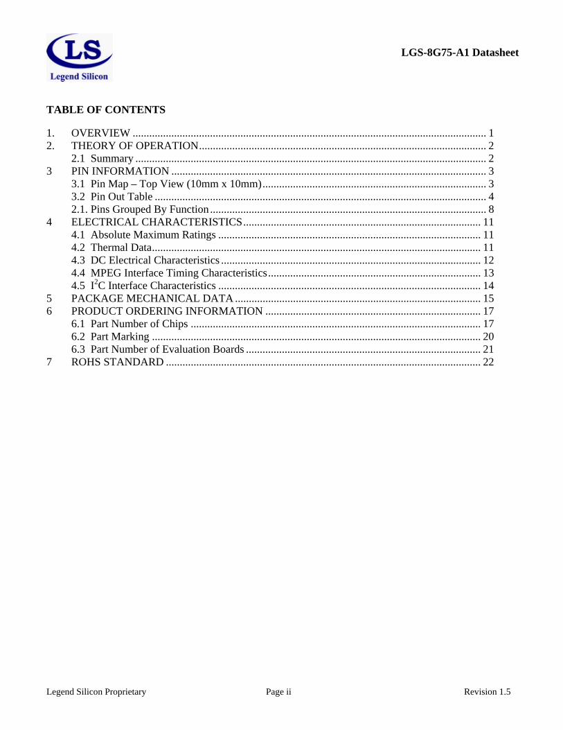
TABLE OF CONTENTS 1. OVERVIEW ................................................................................................................................ 1 2. THEORY OF OPERATION........................................................................................................ 2
2.1 Summary ............................................................................................................................... 2 3 PIN INFORMATION .................................................................................................................. 3
3.1 Pin Map – Top View (10mm x 10mm)................................................................................. 3 3.2 Pin Out Table ........................................................................................................................ 4 2.1. Pins Grouped By Function .................................................................................................... 8
4 ELECTRICAL CHARACTERISTICS...................................................................................... 11 4.1 Absolute Maximum Ratings ............................................................................................... 11 4.2 Thermal Data....................................................................................................................... 11 4.3 DC Electrical Characteristics .............................................................................................. 12 4.4 MPEG Interface Timing Characteristics............................................................................. 13 4.5 I2C Interface Characteristics ............................................................................................... 14
5 PACKAGE MECHANICAL DATA ......................................................................................... 15 6 PRODUCT ORDERING INFORMATION .............................................................................. 17
6.1 Part Number of Chips ......................................................................................................... 17 6.2 Part Marking ....................................................................................................................... 20 6.3 Part Number of Evaluation Boards ..................................................................................... 21
7 ROHS STANDARD .................................................................................................................. 22
LGS-8G75-A1 Datasheet
Legend Silicon Proprietary Page iii Revision 1.5
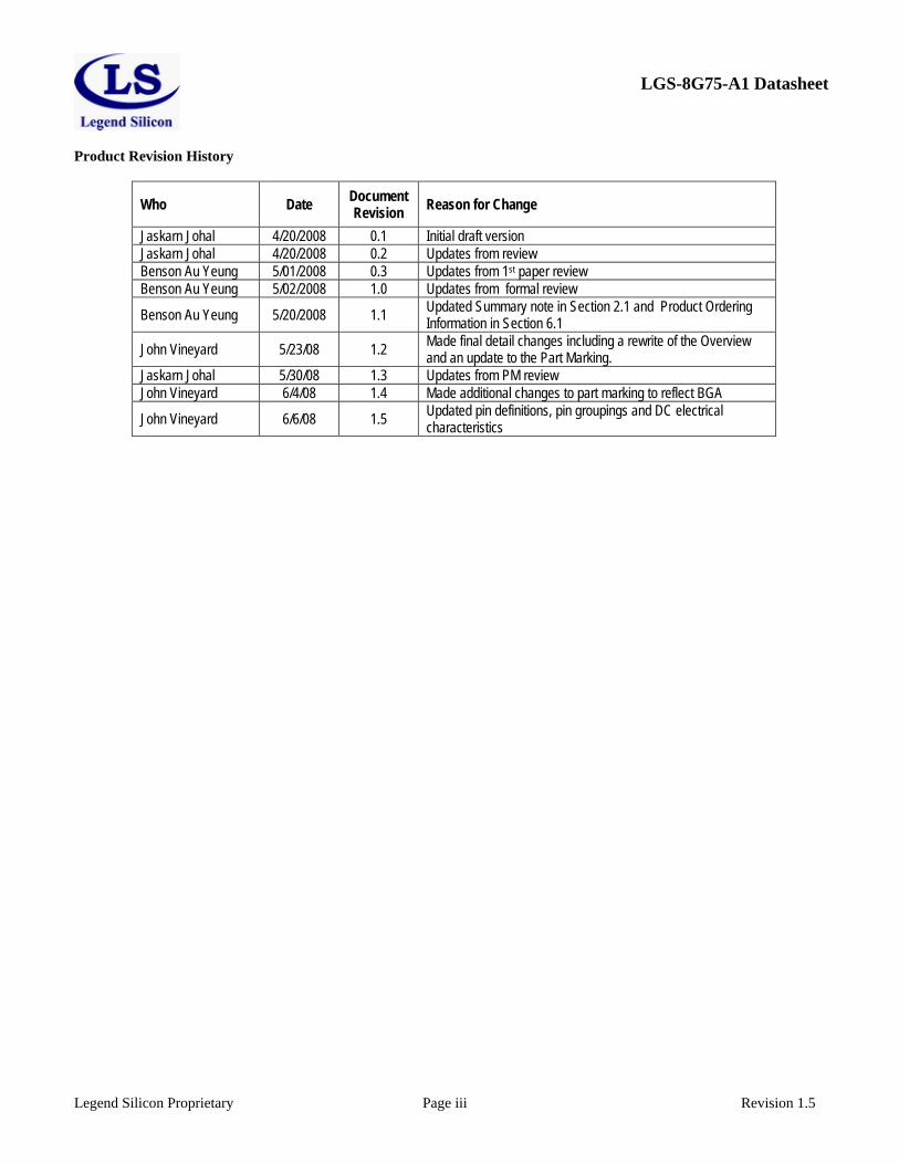
Product Revision History
Who Date Document Revision Reason for Change
Jaskarn Johal 4/20/2008 0.1 Initial draft version Jaskarn Johal 4/20/2008 0.2 Updates from review Benson Au Yeung 5/01/2008 0.3 Updates from 1st paper review Benson Au Yeung 5/02/2008 1.0 Updates from formal review
Benson Au Yeung 5/20/2008 1.1 Updated Summary note in Section 2.1 and Product Ordering Information in Section 6.1
John Vineyard 5/23/08 1.2 Made final detail changes including a rewrite of the Overview and an update to the Part Marking.
Jaskarn Johal 5/30/08 1.3 Updates from PM review John Vineyard 6/4/08 1.4 Made additional changes to part marking to reflect BGA
John Vineyard 6/6/08 1.5 Updated pin definitions, pin groupings and DC electrical characteristics

LGS-8G75-A1 Datasheet
Legend Silicon Proprietary Page 1 Revision 1.5
1. OVERVIEW
The LGS-8G75-A1 is a demodulator IC fully compliant with the China Digital Television Terrestrial Broadcasting System Standard (GB20600-2006). Designed for multi-carrier and single-carrier mobile digital terrestrial reception of high definition, standard definition and other multimedia-based services, the demodulator is optimized for low power and space constrained applications such as portable media players (PMP), Ultra-mobile PCs (UMPC), USB sticks, laptops and cell phones. The LGS-8G75-A1 demodulator features dual integrated analog-to-digital converters (ADC), fully integrated Time De-interleaver memory and is available in a 144 BGA package. It is intended to be a replacement for the LGS-8GL5-A1 demodulator.
The LGS-8G75-A1 takes either baseband or IF signals, performs the necessary demodulation, forward error correction, and provides an MPEG-2 transport stream output in parallel or serial format. With a tuner and an LGS-8G75-A1 demodulator chip a complete RF-to-MPEG front-end system can be implemented, that is fully compliant with GB20600-2006 standard.
The following figure shows a typical receiver application using the LGS-8G75-A1:
KEY FEATURES
• GB20600-2006 compliant single chip demodulator
• Supports 4QAM, 4QAM-NR, 16QAM, 32QAM, and 64QAM modulation for both fixed and mobile applications
• FEC rates of 0.4, 0.6, or 0.8 and guard intervals of PN420, PN595, and PN945
• Time De-interleaving: M=240 or M=720
• Excellent Multi and Single Carrier Performance in present of noise and fading
• Integrated dual 10-bit ADCs
• Integrated Memory for Time De-Interleaver
• MPEG-2 transport stream output in parallel or serial
• Automatic parameter discovery & update
• Full I2C bus support
• 144 BGA (10mm x 10mm), 0.8mm pitch
• Complies with RoHS requirements (Pb-free, or Green)
APPLICATIONS
• Portable media players (PMP), Ultra-mobile PCs (UMPC), USB sticks , laptops and cell phones
APPLICATIONPROCESSOR LGS - 8G75-A1
ExternalMemory
MPEG DECODER
TERRESTRIAL TUNER
VHF / UHFANTENNA
VIDEO OUTPUT AUDIO
OUTPUT
VIDEO OUTPUT AUDIO
OUTPUT

LGS-8G75-A1 Datasheet
Legend Silicon Proprietary Page 2 Revision 1.5
2. THEORY OF OPERATION
2.1 Summary
The LGS-8G75-A1 demodulator uses an external terrestrial tuner that converts the analog VHF/UHF signal through dual internal analog-to-digital converters (ADC). Following conversion to baseband, TDS-OFDM demodulation is performed according to the GB20600-2006 specifications. The output of the channel estimation/correction block is sent to a time de-interleaver and then to the FEC. The output is a parallel or serial MPEG-2 transport stream including data valid, sync, and clock.
The main configurable parameters for GB20600-2006 are:
• Support single-carrier and multi-carrier
• Sub-carrier demodulation: 4QAM-NR, 4QAM, 16QAM, 32QAM, or 64QAM
• Forward error correction rate: 0.4, 0.6, or 0.8
• Guard interval: PN420, PN595, and PN945
• Time De-interleaving: M=240 or M=720.
• Channel bandwidth: 8 MHz
• Internal/external ADC
The following parameters can be automatically detected:
• Guard internal PN420, PN945
• Sub-carrier demodulation
• Forward error correction rate
• Time de-interleaver

LGS-8G75-A1 Datasheet
Legend Silicon Proprietary Page 3 Revision 1.5
3 PIN INFORMATION
3.1 Pin Map – Top View (10mm x 10mm)
RES
I2Q6 Q8
I1Q5 BP2
RESQ3 Q4 Q7 Q9
I6 IPQ2 Q1 I8
IM QPQ0 I5
I0 QMI9 I7 I4 I3
A
B
C
E
F
G
H
D
J
K
L
M
A
B
C
E
F
G
H
D
J
K
L
M
1 2 3 4 5 6 7 8 9 10 11 12
1 2 3 4 5 6 7 8 9 10 11 12
MPEG_D6
MPEG_D7
VDD1.2
VDD2.5
MPEG_SYNC RES VDD
2.5VDD1.2
RES RES
RES
RES RES
DGND MPEG_VALID
RES DGND RES DGND BLKERRN
RES SDAT
MPEG_D5
VDD2.5 RES MPEG
_CLKSHUTDOWN
GPIO1 RES RES LOCK RES DGND SCLT
MPEG_D4
DGND RES RESVDD1.2
VDD2.5 RES SDA RES VDD
2.5
VDD1.2
DGND RES RES DGND RES AGC SCL RES
DGND RES RES RES RES VDD1.2
DGND RES RESETN
MPEG_D2
VDD2.5
CLK_OBS
VDD1.2
VDD2.5
RES DGND RES
MPEG_D1
MPEG_D3 DGND DGND RES RES VDD
2.5
MPEG_D0
ADC_VDD1.2
VBG VDD1.2
CEA0 RES
AGNDPLL_AVDD1.2
XTALIN GPIO0 VDD
2.5DGND
XTALOUT
PLL_VDD1.2
PLL_AGND
DGND VDD2.5 RES RES
PLL_GND DGND RF
AGCIF_CLK RES
RESRES
RES RES
RES
CEA2
RES
IBIAS
CEA1
RES
RES RES
RES
RES RES
RES

LGS-8G75-A1 Datasheet
Legend Silicon Proprietary Page 4 Revision 1.5
3.2 Pin Out Table
• All signal pins are 2.5V LVTTL compatible and 3.3V tolerant.
• All input/output (IO) and output (O) pins can drive 2 mA, unless noted otherwise below.
Pin # Name Type Description A1 RES No connection
A2 MPEG_D6 O MPEG data output Bit6
A3 MPEG_D7 O MPEG data output Bit7 A4 VDD1.2 1.2V 1.2V voltage for digital core A5 VDD2.5 2.5V 2.5V voltage for digital I/O A6 MPEG_SYNC O MPEG sync signal A7 RES No connection A8 VDD2.5 2.5V 2.5V voltage for digital I/O A9 RES No connection A10 VDD1.2 1.2V 1.2V voltage for digital core A11 RES No connection A12 RES No connection B1 RES No connection B2 RES No connection B3 RES No connection B4 DGND Ground Digital ground B5 MPEG_VALID O MPEG data valid signal B6 RES No connection B7 DGND Ground Digital ground B8 RES No connectionB9 DGND Ground Digital ground
B10 BLKERRN O LPDC Block error indicator B11 RES I/O No connection B12 SDAT IO I2C data pass-through for tuner
C1 MPEG_D5 O MPEG data output Bit5
C2 VDD2.5 2.5V 2.5V voltage for digital I/O C3 RES No connection C4 MPEG_CLK O MPEG clock C5 SHUTDOWN O Tuner Shut Down C6 GPIO1 O General purpose IO, control from I2C C7 RES No connection C8 RES No connection C9 LOCK O Demodulator lock signal
C10 RES No connectionC11 DGND Ground Digital ground C12 SCLT O I2C clock pass-through for tuner D1 RES No connection
LGS-8G75-A1 Datasheet
Legend Silicon Proprietary Page 5 Revision 1.5
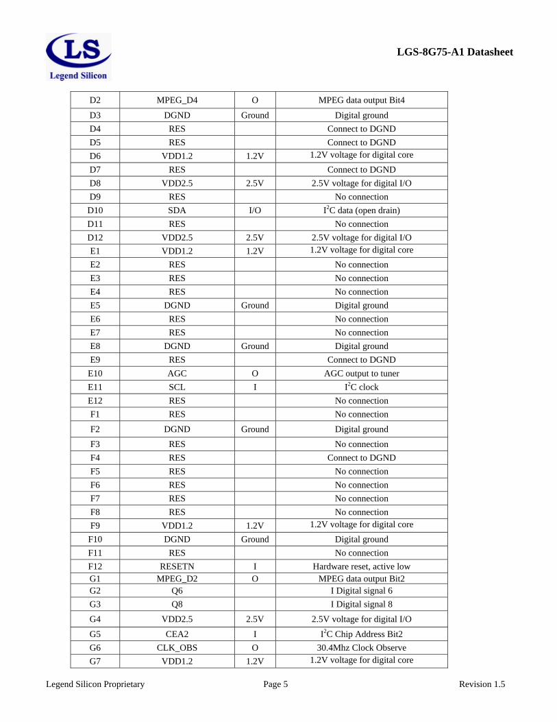
D2 MPEG_D4 O MPEG data output Bit4
D3 DGND Ground Digital ground D4 RES Connect to DGND D5 RES Connect to DGND D6 VDD1.2 1.2V 1.2V voltage for digital core D7 RES Connect to DGND D8 VDD2.5 2.5V 2.5V voltage for digital I/O D9 RES No connection D10 SDA I/O I2C data (open drain) D11 RES No connection D12 VDD2.5 2.5V 2.5V voltage for digital I/O E1 VDD1.2 1.2V 1.2V voltage for digital core E2 RES No connection E3 RES No connection E4 RES No connection E5 DGND Ground Digital ground E6 RES No connection E7 RES No connection E8 DGND Ground Digital ground E9 RES Connect to DGND
E10 AGC O AGC output to tuner E11 SCL I I2C clock E12 RES No connection F1 RES No connection
F2 DGND Ground Digital ground F3 RES No connection F4 RES Connect to DGND F5 RES No connection F6 RES No connection F7 RES No connection F8 RES No connection F9 VDD1.2 1.2V 1.2V voltage for digital core F10 DGND Ground Digital ground F11 RES No connection F12 RESETN I Hardware reset, active low G1 MPEG_D2 O MPEG data output Bit2 G2 Q6 I Digital signal 6 G3 Q8 I Digital signal 8 G4 VDD2.5 2.5V 2.5V voltage for digital I/O
G5 CEA2 I I2C Chip Address Bit2 G6 CLK_OBS O 30.4Mhz Clock Observe G7 VDD1.2 1.2V 1.2V voltage for digital core

LGS-8G75-A1 Datasheet
Legend Silicon Proprietary Page 6 Revision 1.5
G8 I2 I IF/I Digital signal 2 G9 VDD2.5 2.5V 2.5V voltage for digital I/O G10 RES No connection G11 DGND Ground Digital ground G12 RES No connection H1 Q5 I Q Digital signal 5
H2 MPEG_D1 O MPEG data output Bit1
H3 MPEG_D3 O MPEG data output Bit3 H4 BP2 I Connect to DGND H5 DGND Ground Digital ground H6 RES No connection H7 I1 I IF/I Digital signal 1 H8 DGND Ground Digital ground H9 RES Connect to DGND H10 RES No connection H11 RES No connection H12 VDD2.5 2.5V 2.5V voltage for digital I/O J1 Q3 I Q Digital signal 3 J2 Q4 I Q Digital signal 4 J3 MPEG_D0 O MPEG data output Bit0 J4 Q7 I Q Digital signal 7 J5 Q9 I Q Digital signal 9 J6 RES No connection J7 ADC_VDD1.2 1.2V 1.2V Digital for ADC J8 RES No connection J9 VBG Analog Band-gap reference voltage for ADC
J10 VDD1.2 1.2V 1.2V voltage for digital core J11 CEA0 I I2C Chip Address Bit0 J12 RES No connection K1 XTALIN A Crystal input/External Clock input K2 Q2 I Q Digital signal 2 K3 Q1 I Q Digital signal 1 K4 I8 I IF/I Digital signal 8 K5 PLL_AVDD1.2 1.2V 1.2V Analog voltage for PLL K6 I6 I IF/I Digital signal 6 K7 AGND Ground Analog ground for ADC K8 IP A I+ Base Band or IF input K9 CEA1 I I2C Chip Address Bit1 K10 GPIO0 O General purpose IO K11 VDD2.5 2.5V 2.5V voltage for digital I/O K12 DGND Ground Digital ground L1 XTALOUT A Crystal output

LGS-8G75-A1 Datasheet
Legend Silicon Proprietary Page 7 Revision 1.5
L2 Q0 I Q Digital signal 0 L3 PLL_VDD1.2 1.2V 1.2V Digital for PLL L4 PLL_AGND Ground Analog PLL ground L5 I5 I IF/I Digital signal 5 L6 DGND Ground Digital ground L7 IM A I- Base Band or IF input
L8 IBIAS Analog Output to monitor or input to bypass - the internally generated bias current for ADC
L9 QP A Q+ Base Band input L10 VDD2.5 2.5V 2.5V voltage for digital I/O L11 RES Connect to DGND L12 RES No connection M1 I9 I IF/I Digital signal 9 M2 PLL_GND Ground PLL ground M3 I7 I IF/I Digital signal 7 M4 I4 I IF/I Digital signal 4 M5 I3 I IF/I Digital signal 3 M6 I0 I IF/I Digital signal 0 M7 RES No connection M8 QM Analog Q- Base Band input M9 DGND Ground Digital ground
M10 RFAGC O RF AGC output to tuner M11 IF_CLK O External ADC Clock M12 RES Connect to DGND

LGS-8G75-A1 Datasheet
Legend Silicon Proprietary Page 8 Revision 1.5
2.1. Pins Grouped By Function
I2C Interface
Pin # Name Type Description E11 SCL I I2C clock D10 SDA IO I2C data (open drain) C12 SCLT O I2C clock pass-through for tuner B12 SDAT IO I2C data pass-through for tuner
G5, K9, J11 CEA2, CEA1, CEA0 I I2C address selection (3 bits)
Clocks and Resets
Pin # Name Type Description
K1 XTALIN Analog External parallel crystal input, also external clock input
L1 XTALOUT Analog External parallel crystal output F12 RESETN I Hardware reset, active low G6 CLK_OBS O 30.4Mhz clock observation pin H4 BP2 I Connect to DGND for 30.4MHz operation
Tuner & ADC Interface
Pin # Name Type Description L7, K8 IM,IP Analog I-, I+ Base Band input /IF inputs M8, L9 QM,QP Analog Q-, Q+ Base Band input
E10 AGC O AGC output to tuner (PWM format) Active High/Low/Open drain
M10 RFAGC O RF AGC output to tuner (PWM format) Active High/Low/Open drain
L8 IBIAS Analog Output to monitor or input to bypass the internally generated bias current for ADC
J9 VBG Analog Band-gap reference voltage for ADC C5 SHUTDOWN O Tuner shut down
M6, H7, G8, M5, M4, L5, K6, M3,
K4, M1 I0-I9 I IF/I0-I9 digital signal (no connection if not
used)
L2, K3, K2, J1, J2, H1, G2, J4, G3, J5 Q0-Q9 I Q0-Q9 digital signal (no connection if not
used) M11 IF_CLK O Clock for the external ADC

LGS-8G75-A1 Datasheet
Legend Silicon Proprietary Page 9 Revision 1.5
MPEG Interface
Pin # Name Type Description A3, A2, C1, D2, H3, G1, H2, J3
MPEG_D7 – MPEG_D0 O MPEG data outputs in parallel mode
(8 bits, D7 is MSB) A3 MPEG_D7 O MPEG data output in serial mode C4 MPEG_CLK O MPEG clock output B5 MPEG_VALID O MPEG data valid signal A6 MPEG_SYNC O MPEG sync signal
Test Pins & Indicators
Pin # Name Type Description B10 BLKERRN O LPDC Block error indicator, active low C9 LOCK O Demodulator lock signal, active high
K10 GPIO0 O General purpose IO, control from I2C C6 GPIO1 O General purpose IO, control from I2C
Power and Ground
Pin # Name Type Description C2, G4, A5, A8, D8, G9, L10,
K11, D12, H12 VDD2.5 2.5V 2.5V voltage for digital I/O (10 pins)
E1,A4,D6,G7,F9,A10,J10 VDD1.2 1.2V 1.2V voltage for digital core (7 pins)
F2,D3,B4,E5,H5,L6,B7,E8, H8,B9,M9,F10,C11,G11,
K12 DGND Ground Digital ground
(15 pins)
K5 PLL_AVDD1.2 1.2V 1.2V Analog voltage for PLL L4 PLL_AGND Ground Analog PLL ground L3 PLL_VDD1.2 1.2V 1.2V Digital for PLL M2 PLL_GND Ground PLL ground J7 ADC_VDD1.2 1.2V 1.2V Digital for ADC K7 AGND Ground Analog ground for ADC
LGS-8G75-A1 Datasheet
Legend Silicon Proprietary Page 10 Revision 1.5
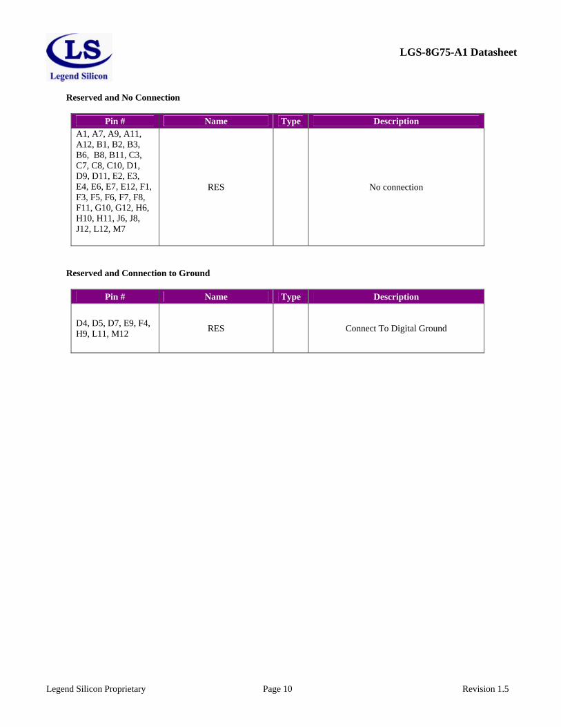
Reserved and No Connection
Pin # Name Type Description A1, A7, A9, A11, A12, B1, B2, B3, B6, B8, B11, C3, C7, C8, C10, D1, D9, D11, E2, E3, E4, E6, E7, E12, F1, F3, F5, F6, F7, F8, F11, G10, G12, H6, H10, H11, J6, J8, J12, L12, M7
RES No connection
Reserved and Connection to Ground
Pin # Name Type Description
D4, D5, D7, E9, F4, H9, L11, M12 RES Connect To Digital Ground

LGS-8G75-A1 Datasheet
Legend Silicon Proprietary Page 11 Revision 1.5
4 ELECTRICAL CHARACTERISTICS
4.1 Absolute Maximum Ratings
Stresses beyond those listed in the table below may cause irreversible damage and/or degradation to the device. Functionality of the device is not guaranteed or implied at these or any other conditions beyond those indicated in the recommended operating conditions.
Parameter Description Value VDD2.5 Max 2.5V power supply voltage 2.75V VDD1.2 Max 1.2V power supply voltage 1.3V
VI Min/Max voltage on input pins -0.5V to VDD2.5 + 0.5V VO Min/Max voltage on output pins -0.5V to VDD2.5+ 0.5V
The device is MSL3 compliant and the ESD is compliant with the 2K HBM (human-body model).
4.2 Thermal Data
Parameter Description Value Tstg Min/Max storage temperature -40°C to 150°C
RthjaNP Junction-ambient thermal resistance TBD °C/W: two layer PCBTBD °C/W: four layer PCB
Toper Min/Max operating ambient temperature, no air flow -40°C to +85°C

LGS-8G75-A1 Datasheet
Legend Silicon Proprietary Page 12 Revision 1.5
4.3 DC Electrical Characteristics
VDD2.5 = 2.5V, VDD1.2 = 1.2V, and an ambient temperature of 25°C unless otherwise specified.
(1) Inputs are 3.3V tolerant.
(2) Test condition is load of 50pF @2mA.
(3) Typical. MC @ 64QAM/0.6/420/720/Partial Iteration. Room Temperature
(4) Minimum MC@ QPSK/0.4/420/720/Partial Iteration. 0ºC Temperature, -5% voltage
(5) Maximum SC@ 32QAM/0.8/595/720/Full Iteration. 70ºC Temperature, +5% voltage
Parameter Description Test Conditions Min (4)
Typical (3)
Max (5)
Unit
VDD2.5 I/O operating voltage 2.5 2.5 2.5 V VDD1.2 Core operating voltage 1.2 1.2 1.2 V
IDD2.5 I/O power supply current Demodulator operating 17 17 17 mA
IDD1.2 Core power supply current Demodulator operating 215 236 617 mA
POPER Power consumption, operation
Demodulator operating 286 326 822 mW
PSTBY Power consumption, standby mode
Demodulator not operating, standby mode
123 135 148 mW
VIL Low level input voltage 0.7 V VIH (1) High level input voltage 1.7 3.6 V VOL Low level output voltage 0.5 V
VOH (2) High level output voltage 2.1 V

LGS-8G75-A1 Datasheet
Legend Silicon Proprietary Page 13 Revision 1.5
4.4 MPEG Interface Timing Characteristics
Parameter Description Min Typical Max UnitfCLK Core operating clock frequency:
8 MHz channel bandwidth, using 30.4 MHz XTAL 60.8 MHztCLK Core operating clock period (1/ fCLK)
8 MHz channel bandwidth 16.4 ns tMPEGCLK MPEG_CLK duty cycle 40 50 60 %
Parallel output timing: register 0xC2 bit [0] = 0
tCKS MPEG_D[7:0], MPEG_SYNC, MPEG_VALID stable before MPEG_CLK falling edge 2* tCLK ns
tCKH MPEG_D[7:0], MPEG_SYNC, MPEG_VALID stable after MPEG_CLK falling edge 2* tCLK ns
Serial output timing: register 0xC2 bit [0] = 1
tCKS MPEG_D7, MPEG_SYNC, MPEG_VALID stable before MPEG_CLK rising edge 2 ns
tCKH MPEG_D[7:0], MPEG_SYNC, MPEG_VALID stable after MPEG_CLK rising edge 3 ns
The MPEG_TS can also be put into tri-state mode by writing a value one to Bit 7 of Register 0x14. This allows multiple demodulators MPEG-TS outputs to be connected together, for applications that require this.
MPEG_CLK
t CKSU
MPEG_D[7:0], MPEG_SYNC, MPEG_VALID
t CKH
SERIAL OUTPUT TIMING
MPEG_CLK
tCKSU
MPEG_D7,MPEG_SYNC,MPEG_VALID
tCKH
PARALLEL OUTPUT TIMING
LGS-8G75-A1 Datasheet
Legend Silicon Proprietary Page 14 Revision 1.5
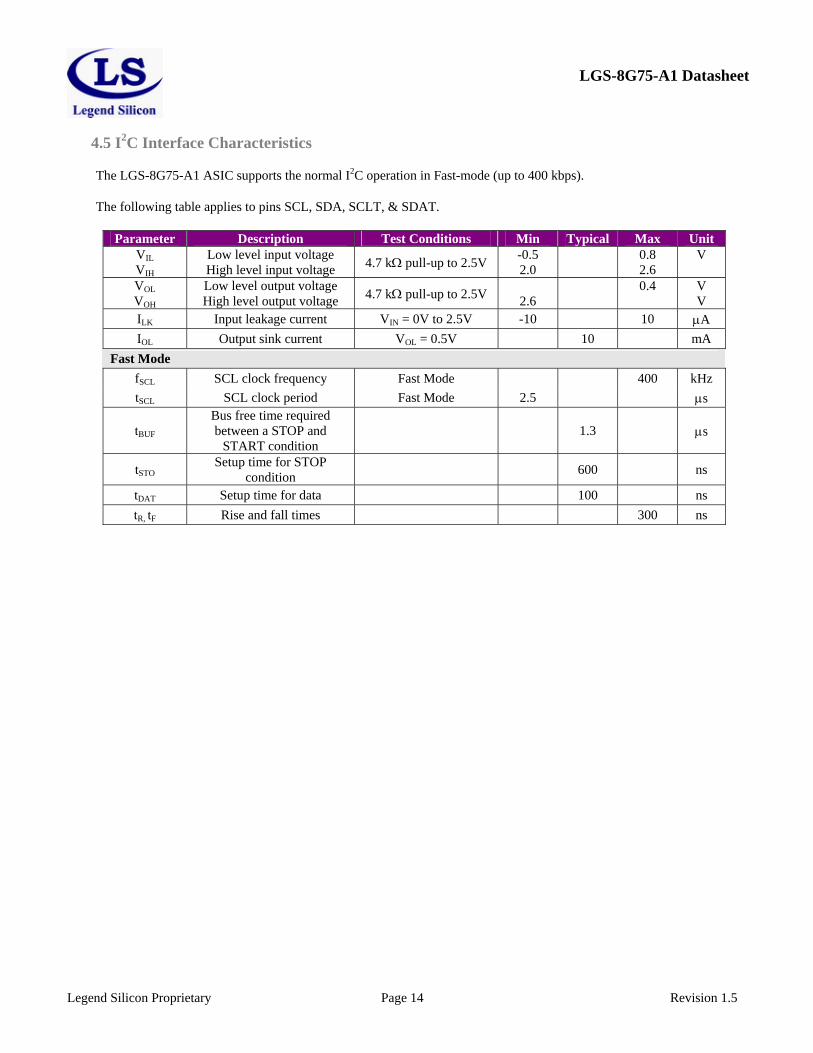
4.5 I2C Interface Characteristics
The LGS-8G75-A1 ASIC supports the normal I2C operation in Fast-mode (up to 400 kbps).
The following table applies to pins SCL, SDA, SCLT, & SDAT.
Parameter Description Test Conditions Min Typical Max UnitVIL VIH
Low level input voltage High level input voltage 4.7 kΩ pull-up to 2.5V -0.5
2.0 0.8
2.6 V
VOL VOH
Low level output voltage High level output voltage 4.7 kΩ pull-up to 2.5V
2.6 0.4
V V
ILK Input leakage current VIN = 0V to 2.5V -10 10 µA IOL Output sink current VOL = 0.5V 10 mA
Fast Mode fSCL SCL clock frequency Fast Mode 400 kHz tSCL SCL clock period Fast Mode 2.5 µs
tBUF Bus free time required between a STOP and
START condition 1.3 µs
tSTO Setup time for STOP condition 600 ns
tDAT Setup time for data 100 ns tR, tF Rise and fall times 300 ns

LGS-8G75-A1 Datasheet
Legend Silicon Proprietary Page 15 Revision 1.5
5 PACKAGE MECHANICAL DATA
The LGS-8G75-A1 ASIC is housed in a 144 pin BGA with dimensions of 10mm x 10mm. An OrCAD symbol of the LGS-8G75-A1 is available from Legend Silicon to facilitate schematic entry and PCB design.
Min Nom Max Min Nom Max
A ----- ----- 1.70 ----- ----- 0.067A1 0.20 0.29 0.38 0.008 0.011 0.015A2 0.84 1.08 1.42 0.033 0.042 0.056c 0.32 0.36 0.40 0.013 0.014 0.016D 9.90 10.00 10.10 0.388 0.392 0.396E 9.90 10.00 10.10 0.388 0.392 0.396D1 ----- 8.80 ----- ----- 0.345 -----E1 ----- 8.80 ----- ----- 0.345 -----e 0.80 0.031b 0.30 0.35 0.40 0.012 0.014 0.016aaabbbcccdddeeeMD/ME
Dimension in inch
12/12 12/120.08
0.0040.0040.0050.0060.003
0.10
Symbol
0.120.15
Dimension in mm
0.10

LGS-8G75-A1 Datasheet
Legend Silicon Proprietary Page 16 Revision 1.5

LGS-8G75-A1 Datasheet
Legend Silicon Proprietary Page 17 Revision 1.5
6 PRODUCT ORDERING INFORMATION
6.1 Part Number of Chips
Standard name and the definition of each part:
LGS-8G75-A1-C-LB1-E
Pro
duct
Fam
ily N
ame
Dev
ice
Type
Func
tion
Pro
cess
Feat
ures
Dev
ice
Rev
isio
n
Tem
pera
ture
Pac
kage
Pac
kage
Fin
ish
Pro
duct
Sta
tus
Table 6-1: Part Number
Section Marking Description Product Family Name
LGS Legend Silicon
Device Type 8 Demodulator Function G Compliant with GB20600-2006 Process 7 90 nm process Features 5 Baseband & IF Device Revision A1 Device revision
Table 6-2: Temperature
Letters Definition Remarks
Blank Not temperature rated Wafer and die sales
C Commercial 0 ºC to +70 ºC E Extended -40C to +70C L Industrial -40C to +85C A Automotive -40C to +85C, Mechanical Shock Certified

LGS-8G75-A1 Datasheet
Legend Silicon Proprietary Page 18 Revision 1.5
Table 6-3: Package
Table 6-4: Package Finish
Table 6-5: Product Status
Letters Definition Remarks Blank None No Package LB LBGA Low Profile BGA PB PBGA Plastic BGA HB HBGA Heat Sink BGA QF QFP Quad Flat Pack LQ LQFP Low Profile QFP TQ TQFP Thin QFP QN QFN Quad Flat Pack - No Leads LE LQFP-E Low Profile QFP Exposed Pad TE TQFP-E Thin QFP Exposed Pad WF Wafer Wafer WP Waffle Pack Die
Letters Definition Remarks Blank No package Wafer and die sales 0 Lead Standard (RoHS 5) 1 Lead-Free RoHS 6 2 Green
Letters Definition Remarks E Engineering Engineering Samples X X Grade Pre-Qualified Devices P Production Production Qualified M Mechanical Mechanical Samples (no die)

LGS-8G75-A1 Datasheet
Legend Silicon Proprietary Page 19 Revision 1.5
Example of available parts:
Partnumber
Pro
duct
Fam
ily N
ame
Dev
ice
Type
Fun
ctio
n
Pro
cess
Fea
ture
s
Dev
ice
Rev
isio
n
Tem
pera
ture
Pac
kage
Pac
kage
Fin
ish
Pro
duct
Sta
tus
LGS-8G75-A1-C-LB1-PCommercial(0ºC to 70ºC)
Pb_FreeRoHS 6
LGS-8G75-A1-L-LB1-PIndustrial-40ºC to 85ºC
Pb_FreeRoHS 6
LGS-8G75-A1-A-LB1-PAutomotive-40ºC to 85ºC
Pb_FreeRoHS 6
LGS-8G75-A1-C-LB2-PCommercial(0ºC-70ºC) Green
LGS-8G75-A1-L-LB2-PIndustrial-40ºC to 85ºC Green
LGS-8G75-A1-A-LB2-PAutomotive-40ºC to 85ºC Green
DemodChip
TerrestrialDemodulator GB20600-2006 90nm BASEBAND
& IF A1Low
ProfileBGA
ProductionQualified
Chip
Note: Please contact Legend Silicon before ordering for correct product status number.
LGS-8G75-A1 Datasheet
Legend Silicon Proprietary Page 20 Revision 1.5
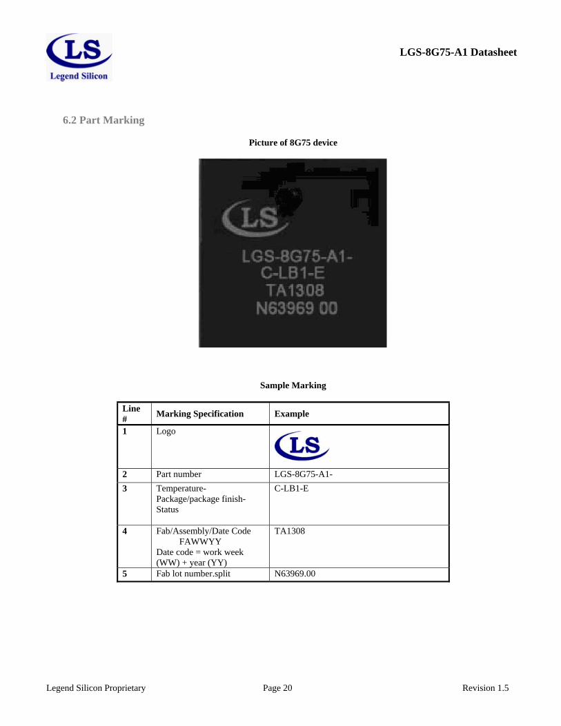
6.2 Part Marking
Picture of 8G75 device
Sample Marking
Line # Marking Specification Example
1 Logo
2 Part number LGS-8G75-A1- 3 Temperature-
Package/package finish-Status
C-LB1-E
4 Fab/Assembly/Date Code FAWWYY
Date code = work week (WW) + year (YY)
TA1308
5 Fab lot number.split N63969.00

LGS-8G75-A1 Datasheet
Legend Silicon Proprietary Page 21 Revision 1.5
6.3 Part Number of Evaluation Boards
Standard name and the definition of each part:
LGR-H4-0A2-A2
Pro
duct
Fam
ily N
ame
Dev
ice
Type
LS P
rodu
ct
Tune
r/Par
tner
Inte
rface
s
Boa
rd R
evis
ion
Available Evaluation Boards and the detail description of each part:
Partnumber
Prod
uct F
amily
Nam
e
Dev
ice
Type
LS P
rodu
ct
Inte
rfac
es
Tune
r/Par
tner
Boa
rd R
evis
ion
LGR-H4-0A2-A2 EvaluationBoard 8G75-A1 MPEG-TS
ADI TunerADMTV102 A2
Module
LGR-F0-G00-A2 EvaluationBaseBoard Multiple
MPEG-TSUSBSDIO
Multiple A2
LegendSiliconEval
Board
LegendSiliconEval
Board

LGS-8G75-A1 Datasheet
Legend Silicon Proprietary Page 22 Revision 1.5
7 ROHS STANDARD
RoHS system has three different levels, RoHS 5, RoHS6, and Green. The following graph gives detail information:
Green PackageChromium Cadmium Mercury PBB PDE
Lead Asbestos Azo Colorants Ozone depleting Class I & II PCB Polychlorinated
Napthalenes Radioactive Tributyl Tin Arsenic Short Chain Chlorinated Paraffins Tiphenyl Tin Tributyl Tin Oxide Antimony
Beryllium Bimuth Bromated Flame
Pb-Free RoHS 6
Chromium Cadmium Mercury
PBB PDE Lead
Standard RoHS 5
Chromium Cadmium Mercury
PBB PDE
Items removed from the package processing


