
Lighting the Way: A Micro-Symposium on Current Research at the Photonics
Center
September 28, 2015
Roberto Paiella
Electrical and Computer Engineering

Plasmon-Enhanced OptoelectronicsPlasmon enhanced light emission from LED active materials
Optical nanoantennas for directional emission and photodetection
LUMINESCENCE SPECTRA-60
-50-40
-30-20-10 0 10 20 3040
5060
-60-50
-40-30
-20-10 0 10 2030
4050
60
FAR-FIELD RADIATION PATTERNS
from Wikipedia
APPLICATIONS TO ARTIFICIAL COMPOUND EYES

Siddharth Ramachandran
Electrical and Computer Engineering
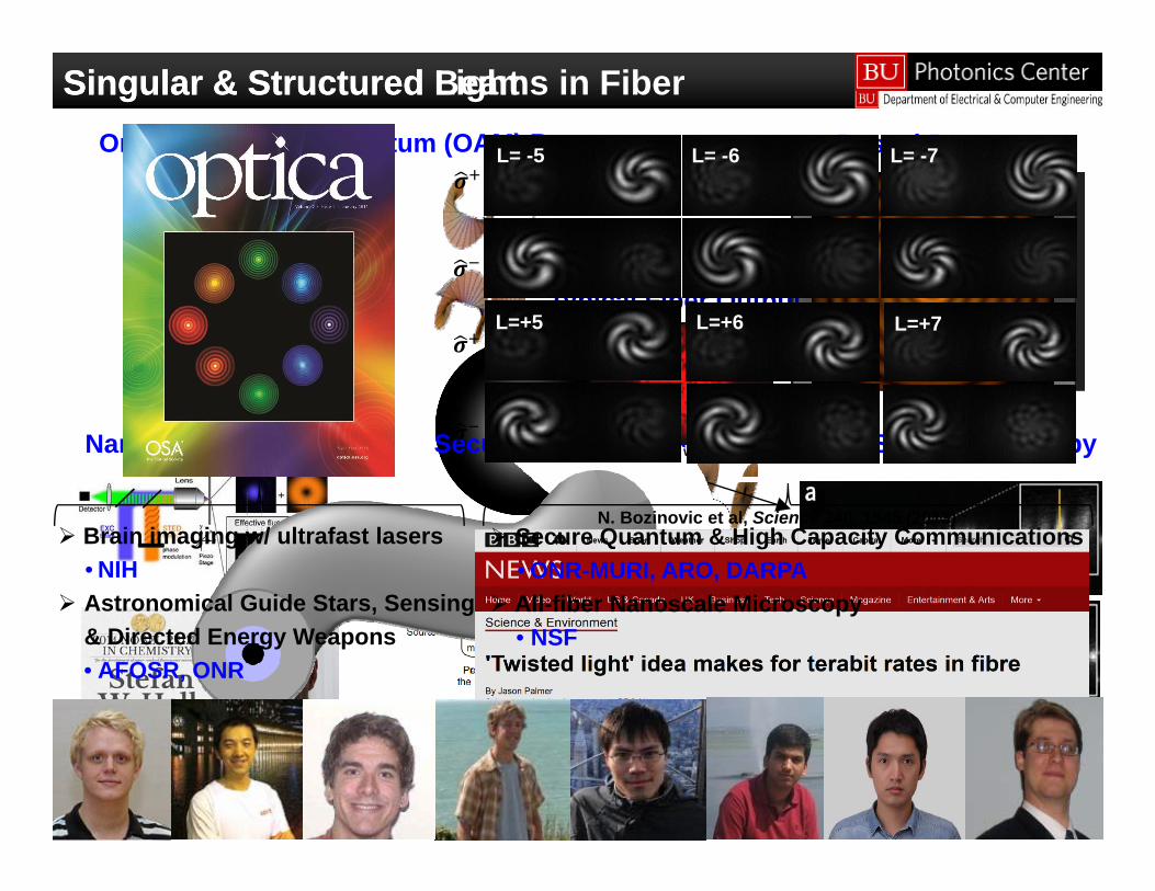
Singular & Structured Light
T.A. Planchon et al, Nature Methods8, 417 (2011)
Orbital Angular Momentum (OAM) Beams Bessel Beams
Vaziri et al, Phys. Rev. Lett. 89 (2002)
S. Hell & J. Wichmann, Opt. Lett. 19, 780 (1994)
A conventionalGaussian BeamNanoscale Microscopy Secure Quantum Comm. Light Sheet Microscopy
Singular & Structured Beams in Fiber
Typical Fiber Output
Vadim Makarov www.vad1.com
L= -5 L= -6 L= -7
L=+5 L=+6 L=+7
N. Bozinovic et al, Science 340, 1545 (2013) Brain imaging w/ ultrafast lasers
• NIH Astronomical Guide Stars, Sensing
& Directed Energy Weapons• AFOSR, ONR
Secure Quantum & High Capacity Communications• ONR-MURI, ARO, DARPA
All-fiber Nanoscale Microscopy• NSF

Xin Zhang
Mechanical Engineering

Positive vs negative refractive index
Metamaterials: Controlling light and many applications such as invisibility cloaking and perfect absorption
THz Screening
Mobile phone600MHz – 2.6GHz
Microwave2.4GHz
WIFI2.4GHz
Radar1GHz – 100GHz
Night Vision10 – 0.7 µm
Gas analyzer25– 1 µm
Remoter850nm
CCD300–800nm
Microscope300–800nm
Optical Storage300–800nmTHz comm.
THz imaging
20 m10 m

Bjoern Reinhard
Chemistry

9
Reinhard Lab: Elucidating and Controlling Life at the Nanoscale through Bioplasmonics
L
D

Lee Goldstein
Psychiatry

Jerome Mertz
Biomedical Engineering

Imaging in Complex Media
Luminescent object Spectrum
SSE
Spectral encoder
To camera LED
LED
Phase imaging in thick tissue
Microscopy with Adaptive Optics
Endoscopy through single fiber
in collaboration with Bifano Lab
Jerome Mertz, BME Department
Spectrograph

Scott Bunch
Mechanical Engineering

Experimental mechanical and electrical characterization of atomic membranes
SEM image
Pushing the limits of MEMS
Atomic Membrane Lab
S.P. Koenig et al., NatureNanotechnology, 7, 728-732(2012)
Adhesion Gas Separation Devices and other 2D Materials
X. Liu et al. Advanced Materials,26, 1571-1576 (2014)
L. Wang et al. Nano Letters,12, 3706-3710 (2012)
S.P. Koenig et al. NatureNanotechnology, 6, 543–546 (2011)
X. Liu et al. Nano Letters, 13,2309-2313 (2013)
J.S. Bunch and Martin L. DunnSolid State Communications152, 1359–1364 (2012)
N. Boddetti et al. Journal of Applied Mechanics, 80,040909 (2013)
N. Boddeti et al. NanoLetters, 13, 6216-6221 (2013)
L. Wang et al., NatureNanotechnology, 10, 785-790(2015)
B. Radisavljevic et al, Nature Nano, 2011
Shyamsunder Erramilli
Physics
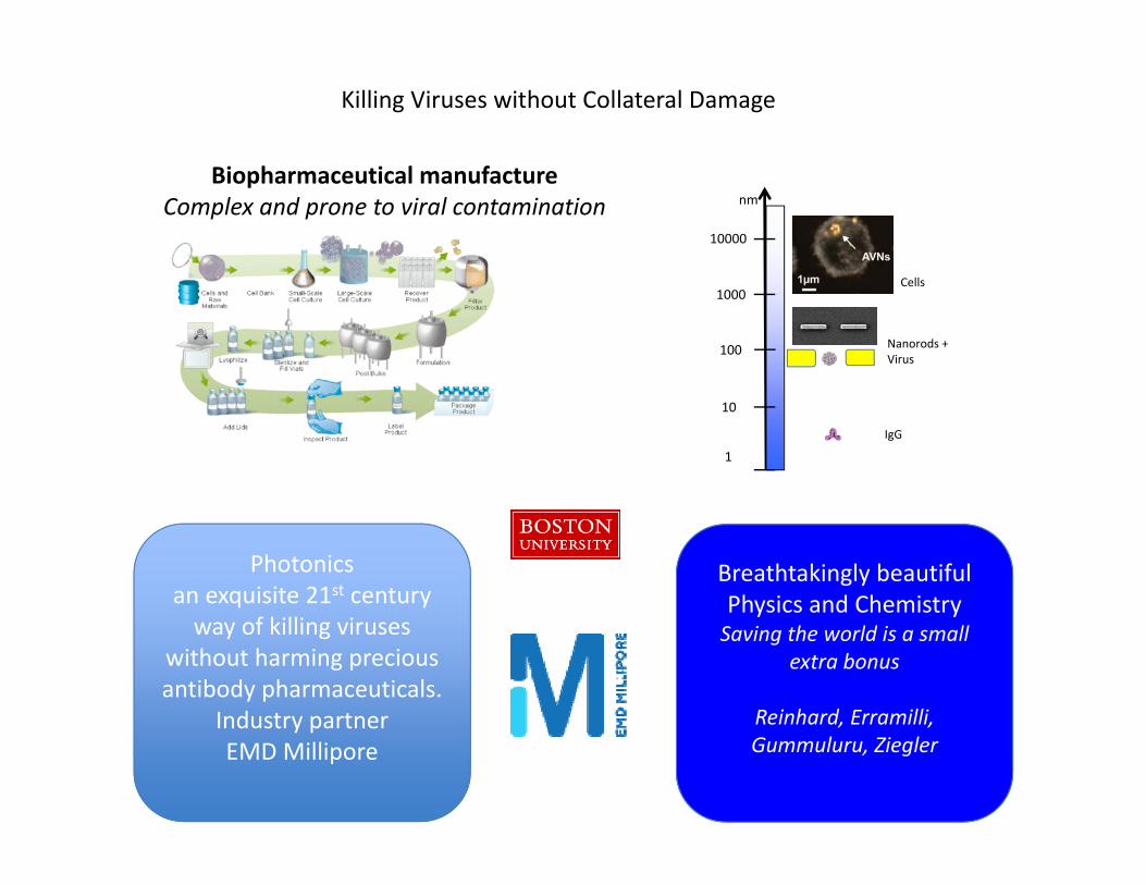
Killing Viruses without Collateral Damage
1
nm
10
100
1000
10000
IgG
Nanorods +Virus
Cells
Photonicsan exquisite 21st century way of killing viruses
without harming precious antibody pharmaceuticals.
Industry partnerEMD Millipore
Breathtakingly beautiful Physics and ChemistrySaving the world is a small
extra bonus
Reinhard, Erramilli, Gummuluru, Ziegler
Biopharmaceutical manufactureComplex and prone to viral contamination

Christopher Gabel
Medicine
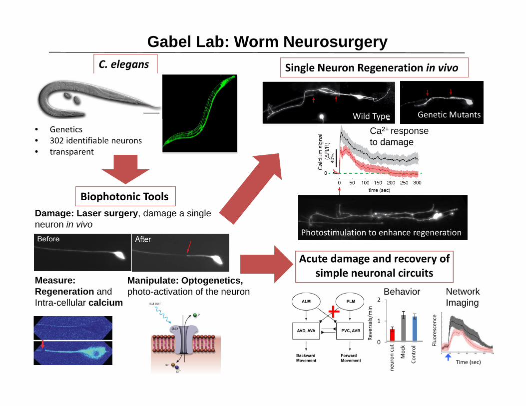
Gabel Lab: Worm Neurosurgery
Acute damage and recovery of simple neuronal circuits
C. elegans
Measure: Regeneration and Intra-cellular calcium
Damage: Laser surgery, damage a single neuron in vivo
0
1
2
Biophotonic Tools
Single Neuron Regeneration in vivo
neuron
cut
Manipulate: Optogenetics, photo-activation of the neuron
Wild Type Genetic Mutants
Photostimulation to enhance regeneration
• Genetics• 302 identifiable neurons• transparent
Ca2+ response to damage
Mock
Control
Behavior Network Imaging
Time (sec)Re
versals/min
Fluo
rescen
ce

David Bishop
Electrical and Computer Engineering

21
Goal:To be able to “paint” a room with both light and data. We want to create low cost technologies to
sculpt the light and data profiles in a room, allowing us to unobtrusively
and responsively meet the occupants’ ever evolving needs.
Painting with Light and
*Collaborators are Tom Little, Jessica Morrison and Corey Pollock

Aaron Schmidt
Mechanical Engineering

Allison Dennis
Biomedical Engineering
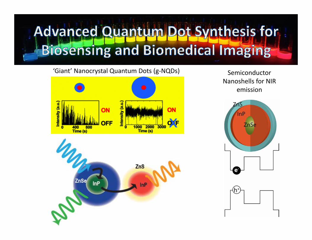
Semiconductor Nanoshells for NIR
emission
‘Giant’ Nanocrystal Quantum Dots (g‐NQDs)

Selim Unlu
Electrical and Computer Engineering
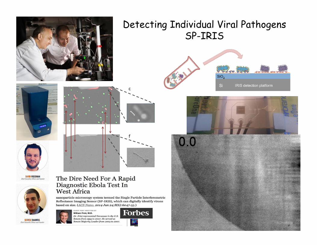
Detecting Individual Viral PathogensSP-IRIS
Joshua Semeter
Electrical and Computer Engineering
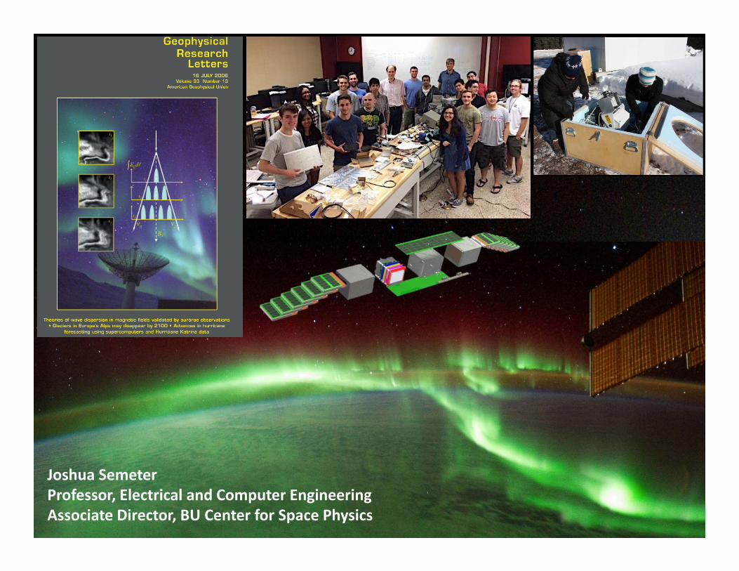
Joshua SemeterProfessor, Electrical and Computer EngineeringAssociate Director, BU Center for Space Physics

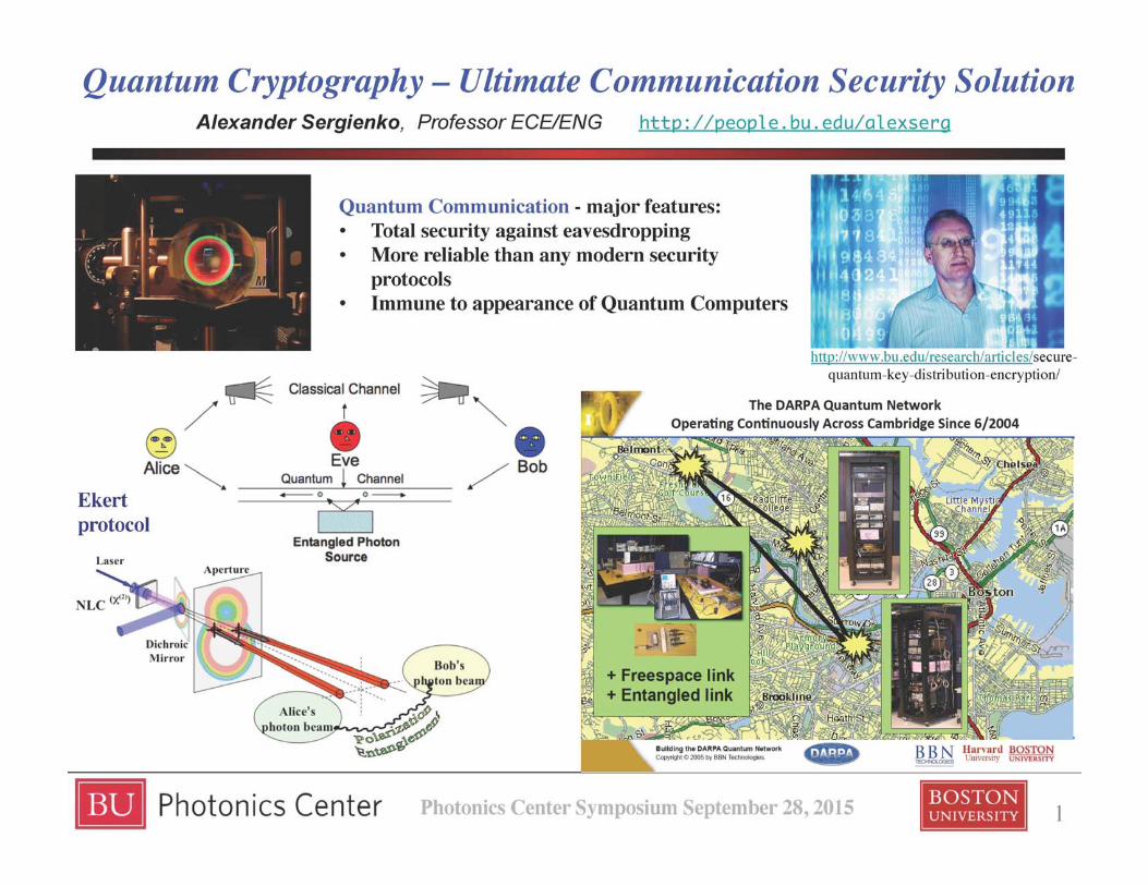
Alexander Sergienko
Electrical and Computer Engineering
Luca Dal Negro
Electrical and Computer Engineering
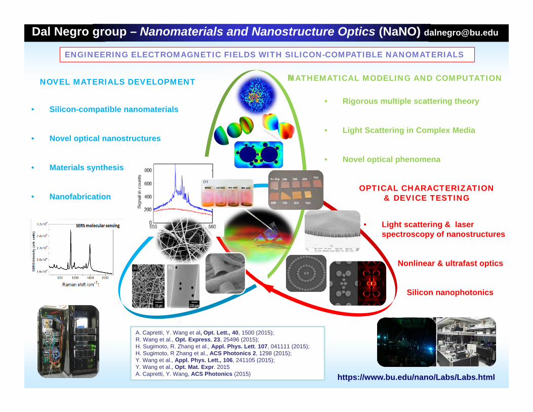
• Light scattering & laser spectroscopy of nanostructures
• Nonlinear & ultrafast optics
Silicon nanophotonics
Dal Negro group – Nanomaterials and Nanostructure Optics (NaNO) [email protected]
NOVEL MATERIALS DEVELOPMENT MATHEMATICAL MODELING AND COMPUTATION
OPTICAL CHARACTERIZATION& DEVICE TESTING
https://www.bu.edu/nano/Labs/Labs.html
ENGINEERING ELECTROMAGNETIC FIELDS WITH SILICON-COMPATIBLE NANOMATERIALS
• Silicon-compatible nanomaterials
• Novel optical nanostructures
• Materials synthesis
• Nanofabrication
• Rigorous multiple scattering theory
• Light Scattering in Complex Media
• Novel optical phenomena
A. Capretti, Y. Wang et al, Opt. Lett., 40, 1500 (2015); R. Wang et al., Opt. Express, 23, 25496 (2015); H. Sugimoto, R. Zhang et al., Appl. Phys. Lett. 107, 041111 (2015); H. Sugimoto, R Zhang et al., ACS Photonics 2, 1298 (2015); Y. Wang et al., Appl. Phys. Lett., 106, 241105 (2015); Y. Wang et al., Opt. Mat. Expr. 2015A. Capretti, Y. Wang, ACS Photonics (2015)

Anna Swan
Electrical and Computer Engineering

Manipulating 2D material properties using friction and strain
L. Wang et al., Science 342, 614 (2013)
2D materials over holes Graphene MEMS device
Strain Engineering THz Emission Pseudo Magnetic Field
Mono‐ Bi‐LayerTri‐
Graphene
Phosphoreneh‐BNMoS2graphene Transferring 2D materials
Darren Roblyer
Biomedical Engineering

Flex Circuit
Probe Housing Bottom View
purely absorbing with scatter
Tumor (4.5cm)
Zakhireh et al., 2008, EJC
Before Chemo
After Chemo

Thank you!


