

Possible applications of Lattice Boltzmann Methods to ASML
Semiconductor Lithography problems
Lorentz Workshop 17 February 2011
Ramin Badie, Nico ten Kate

Slide 2 |
About ASML
• ASML produces lithography machines for the semiconductor industry
• Our lithography is based on optical projection critical for high speed high resolution production of ICs
• The latest production lithography machines are based on
immersion lithography using a thin layer of water between the last lens element and the wafer
• Future production is envisaged to be based on EUV technology that involves operation at very low pressure

Slide 3 |
ASML manufactures optical lithography machines;
lithography is at the heart of chip manufacturing
Repeat 30 to 40 times to build 3
dimensional structure
Slide 4 |
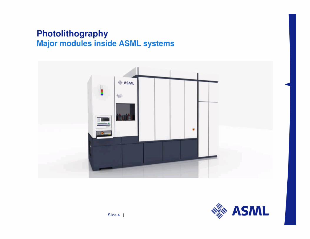
PhotolithographyMajor modules inside ASML systems
Slide 5 |
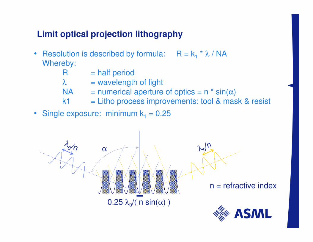
Limit optical projection lithography
• Resolution is described by formula: R = k1 * λ / NAWhereby:
R = half period
λ = wavelength of lightNA = numerical aperture of optics = n * sin(α) k1 = Litho process improvements: tool & mask & resist
• Single exposure: minimum k1 = 0.25
λ0 /n λ0
/nα
0.25 λ0/( n sin(α) )
n = refractive index

Slide 6 |
Extreme UV Lithography

Slide 7 |
Rarefied gas flow and heat transfer in Extreme UV
Lithography

Slide 8 |
Rarefied gas flow and heat transfer in Extreme UV
Lithography

Slide 9 |
DSMC caluclations

Slide 10 |
Modeling
• Conventional use of CFD codes using FEM and FVM with modifications for low pressure are not adequate
• Present DSMC methods give not satisfactory results with respect to the measurements
• A full model for solving gas flow and heat transfer at the
walls would be helpful for finding optimal design rules for this part of the machine

Slide 11 |
Immersion lithography
Lens
Water
Lens
Air

Slide 12 |
Thin film liquid break-up
Redistribution of drop
patterns
Continuous film
fluid
lens
wafer
Scanning stage

Slide 13 |
Evaporation at the meniscus
fluid
lens
wafer
Scanning stage


