
LOW POWER TEST
METHODOLOGY
July 28, 2009
Swapnil Bahl, R. Mattiuzzo, A. Garg, S. Graniello, M. Sautier & D. Appello
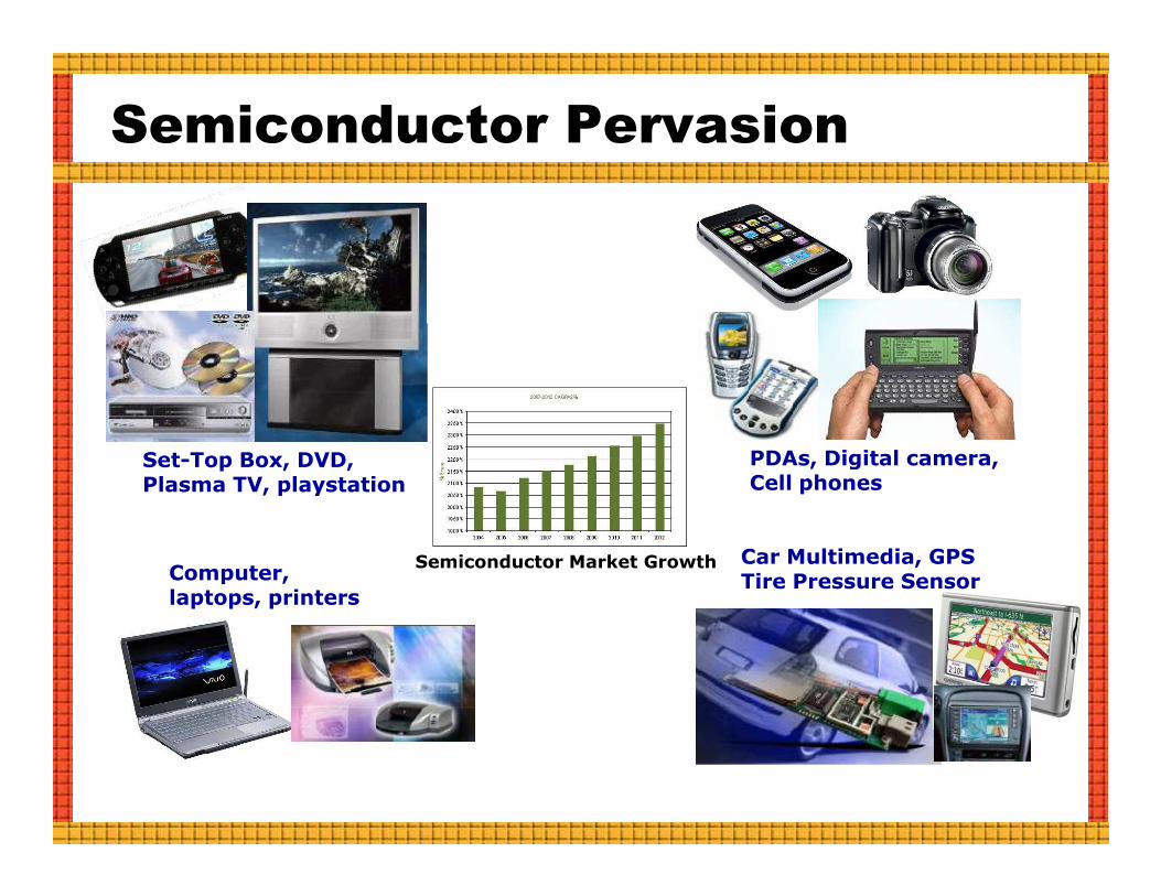
Semiconductor Pervasion
PDAs, Digital camera,Set-Top Box, DVD,
Car Multimedia, GPSTire Pressure Sensor
PDAs, Digital camera,Cell phones
Computer, laptops, printers
Set-Top Box, DVD, Plasma TV, playstation
Semiconductor Market Growth
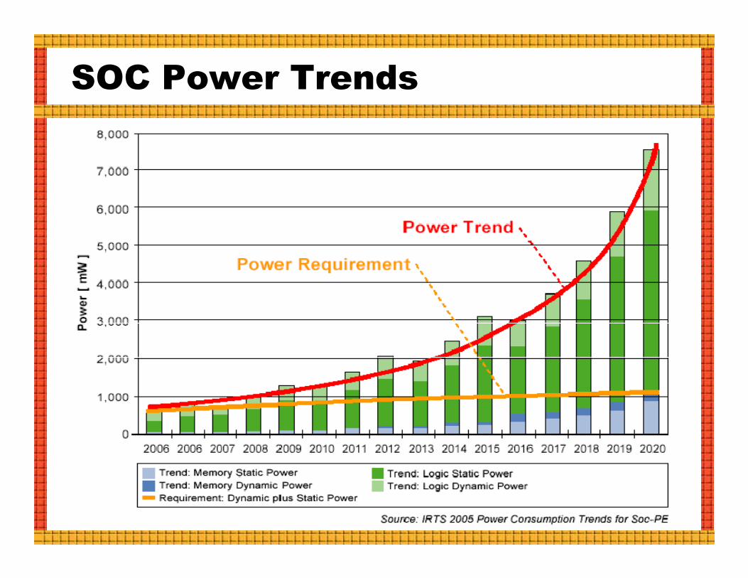
SOC Power Trends
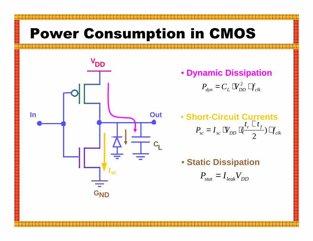
Power Consumption in CMOS
• Dynamic Dissipation
• Short-Circuit Currentstt +
clkDDLdyn fVCP ⋅⋅= 2
VDD
In Out • Short-Circuit Currents
• Static Dissipation
DDleakstat VIP =
clkfr
DDscsc ftt
VIP ⋅+
⋅⋅= )2
(
CL
ISC
NDG
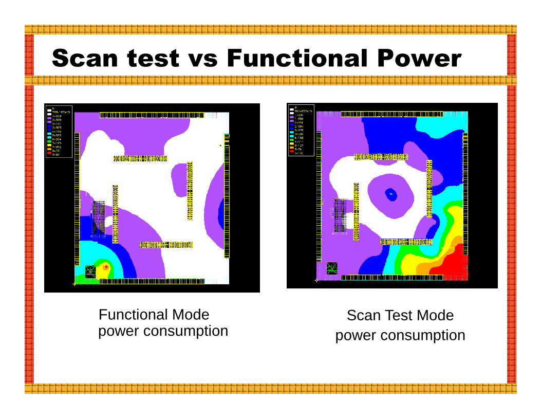
Scan test vs Functional Power
Functional Mode power consumption
Scan Test Modepower consumption
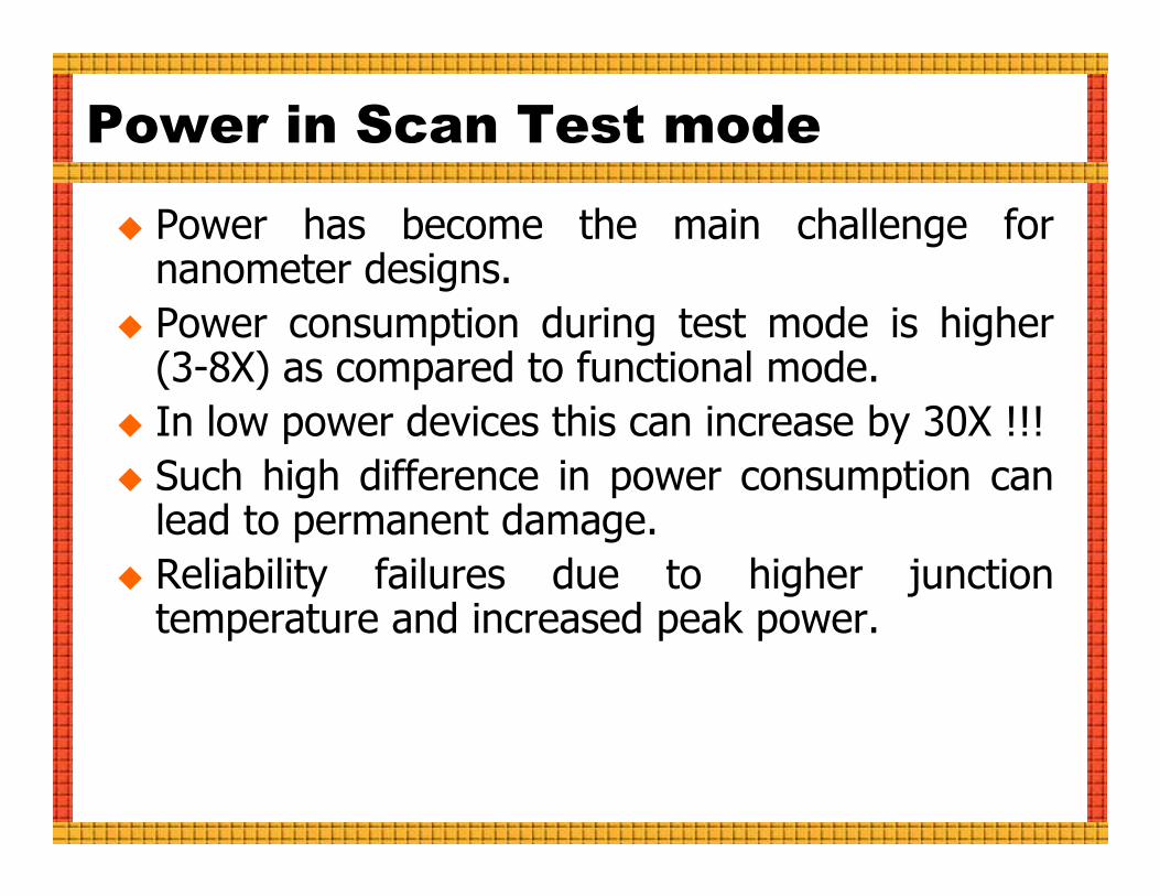
Power in Scan Test mode
� Power has become the main challenge fornanometer designs.
� Power consumption during test mode is higher(3-8X) as compared to functional mode.
� In low power devices this can increase by 30X !!!
� Such high difference in power consumption canlead to permanent damage.
� Reliability failures due to higher junctiontemperature and increased peak power.
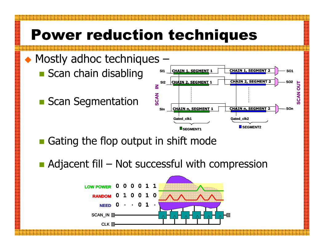
Power reduction techniques
� Mostly adhoc techniques –
� Scan chain disabling
� Scan Segmentation
SI1 SO1
SI2 SO2
SIn SOn
Gated_clk1 Gated_clk2
CHAIN n, SEGMENT 1
SC
AN
IN
SC
AN
OU
T
SEGMENT2
CHAIN 2, SEGMENT 1 CHAIN 2, SEGMENT 2
CHAIN 1, SEGMENT 1 CHAIN 1, SEGMENT 2
CHAIN n, SEGMENT 2
SI1 SO1
SI2 SO2
SIn SOn
Gated_clk1 Gated_clk2
CHAIN n, SEGMENT 1
SC
AN
IN
SC
AN
OU
T
SEGMENT2
CHAIN 2, SEGMENT 1 CHAIN 2, SEGMENT 2
CHAIN 1, SEGMENT 1 CHAIN 1, SEGMENT 2
CHAIN n, SEGMENT 2
� Gating the flop output in shift mode
� Adjacent fill – Not successful with compression
CLK
SCAN_IN
0 · · 0 1 ·NEED
RANDOM 0 1 0 0 1 0
0 0 0 0 1 1LOW POWER
CLK
SCAN_IN
0 · · 0 1 ·NEED
RANDOM 0 1 0 0 1 0
0 0 0 0 1 1LOW POWER
CLK
SCAN_IN
0 · · 0 1 ·NEED 0 · · 0 1 ·NEED
RANDOM 0 1 0 0 1 0RANDOM 0 1 0 0 1 0
0 0 0 0 1 1LOW POWER 0 0 0 0 1 1LOW POWER
SEGMENT1 SEGMENT2SEGMENT1 SEGMENT2
Low Power Test Methodology
� Low Power Test methodology consists of two stages –
� Scan insertion
Pattern generation� Pattern generation
Scan insertion in Low Power designs
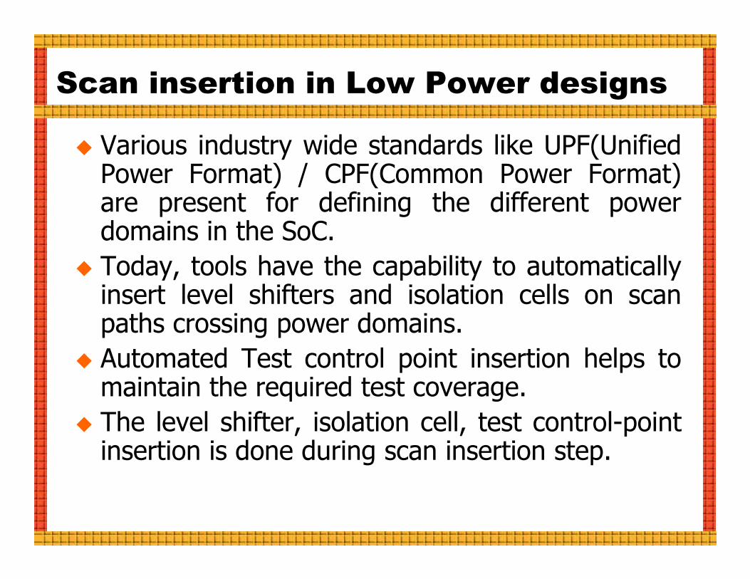
� Various industry wide standards like UPF(UnifiedPower Format) / CPF(Common Power Format)are present for defining the different powerdomains in the SoC.
� Today, tools have the capability to automaticallyinsert level shifters and isolation cells on scaninsert level shifters and isolation cells on scanpaths crossing power domains.
� Automated Test control point insertion helps tomaintain the required test coverage.
� The level shifter, isolation cell, test control-pointinsertion is done during scan insertion step.

Synthesis
RTL
Logical libraries (Power attributes)
UPF
/CPF
Test-readynetlist
UPF
/CPF
DFT in Low Power design flow
(Power attributes)
Multi voltage, OP conditionsISO cell, level shifter, DRR (Data retention registers)
GDSII
Scan Insertion
DFT-insertednetlist
UPF
/CPF
Physical ImplementationPhysical libraries (Power attributes)
Power rail, voltage island,Power switch

Power distribution analysis
� Design statistics –� Division - Automotive
� Technology 90nm.
� 1000K design,50K flops.
� 8Mhz shift frequency.31%
14%33%
22%
Shift Mode
31%
14%33%
22%
Shift Mode
12capturemode
20%
5%
28%
47%
22%
Capture Modecapturemode
20%
5%
28%
47%
22%
Capture Mode
0
2
4
6
8
10
12
Power
in
mW
Shift Capture
Test mode
Combo logic
Sequential logic
Clock network
Hard logic

ATPG Capture Power Reduction
Clock gating implementation
� ATPG can control the clock gating logic to clock only those flops that need to switch/store new data.
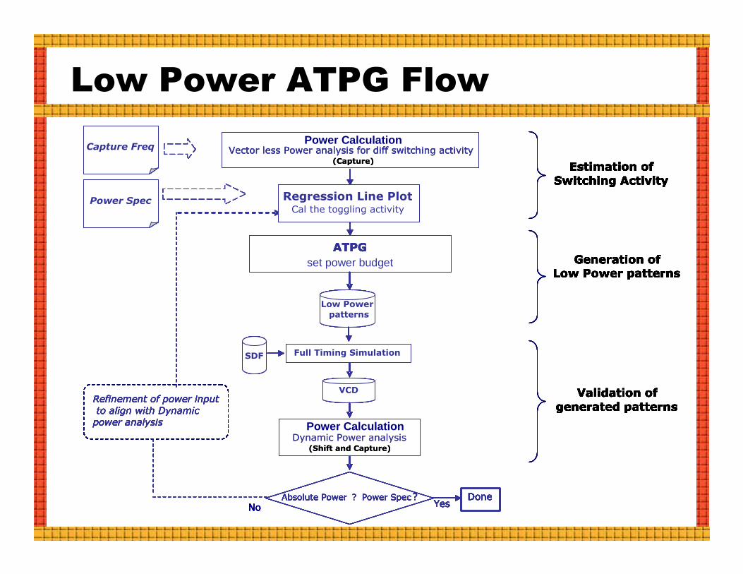
Low Power ATPG Flow
Vector less Power analysis for diff switching activity(Capture)
ATPG
Power Spec Regression Line PlotCal the toggling activity
Capture Freq
Estimation of
Switching Activity
Generation of
Low Power patterns
Vector less Power analysis for diff switching activity(Capture)
ATPG
Power Spec Regression Line PlotCal the toggling activity
Capture Freq
Estimation of
Switching Activity
Generation of
Low Power patternsset power budget
Vector less Power analysis for diff switching activity(Capture)
ATPG
Power Spec Regression Line PlotCal the toggling activity
Capture Freq
Estimation of
Switching Activity
Generation of
Low Power patterns
Vector less Power analysis for diff switching activity
ATPG
Power Spec Regression Line PlotCal the toggling activity
Capture Freq
Estimation of
Switching Activity
Generation of
Low Power patterns
Power CalculationVector less Power analysis for diff switching activity
(Capture)
ATPG
Power Spec Regression Line PlotCal the toggling activity
Capture Freq
Estimation of
Switching Activity
Generation of
Low Power patterns
Vector less Power analysis for diff switching activity(Capture)
ATPG
Power Spec Regression Line PlotCal the toggling activity
Capture Freq
Estimation of
Switching Activity
Generation of
Low Power patternsset power budget
Vector less Power analysis for diff switching activity(Capture)
ATPG
Power Spec Regression Line PlotCal the toggling activity
Capture Freq
Estimation of
Switching Activity
Generation of
Low Power patterns
Vector less Power analysis for diff switching activity
ATPG
Power Spec Regression Line PlotCal the toggling activity
Capture Freq
Estimation of
Switching Activity
Generation of
Low Power patterns
Power Calculation
DoneYes
Low Power
patterns
SDF
VCD
Absolute Power ? Power Spec?
Full Timing Simulation
No
Refinement of power input
to align with Dynamic
power analysis
Dynamic Power analysis(Shift and Capture)
Validation of
generated patterns
Low Power
patterns
SDF
VCD
Absolute Power ? Power Spec?
Full Timing Simulation
No
Refinement of power input
to align with Dynamic
power analysis
Dynamic Power analysis(Shift and Capture)
Validation of
generated patterns
DoneYes
DoneYes
DoneYes
Low Power
patterns
SDF
VCD
Absolute Power ? Power Spec?
Full Timing Simulation
No
Refinement of power input
to align with Dynamic
power analysis
Validation of
generated patterns
Low Power
patterns
SDF
VCD
Absolute Power ? Power Spec?
Full Timing Simulation
No
Refinement of power input
to align with Dynamic
power analysis
Validation of
generated patterns
DoneYes
DoneYes
Power Calculation
DoneYes
DoneYes
Low Power
patterns
SDF
VCD
Absolute Power ? Power Spec?
Full Timing Simulation
No
Refinement of power input
to align with Dynamic
power analysis
Dynamic Power analysis(Shift and Capture)
Validation of
generated patterns
Low Power
patterns
SDF
VCD
Absolute Power ? Power Spec?
Full Timing Simulation
No
Refinement of power input
to align with Dynamic
power analysis
Dynamic Power analysis(Shift and Capture)
Validation of
generated patterns
DoneYes
DoneYes
DoneYes
DoneYes
DoneYes
DoneYes
Low Power
patterns
SDF
VCD
Absolute Power ? Power Spec?
Full Timing Simulation
No
Refinement of power input
to align with Dynamic
power analysis
Validation of
generated patterns
Low Power
patterns
SDF
VCD
Absolute Power ? Power Spec?
Full Timing Simulation
No
Refinement of power input
to align with Dynamic
power analysis
Validation of
generated patterns
DoneYes
DoneYes
DoneYes
DoneYes
Power Calculation
Vectoless Power Estimation
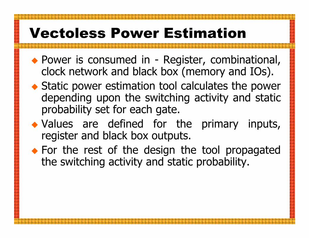
� Power is consumed in - Register, combinational,clock network and black box (memory and IOs).
� Static power estimation tool calculates the powerdepending upon the switching activity and staticprobability set for each gate.
Values are defined for the primary inputs,� Values are defined for the primary inputs,register and black box outputs.
� For the rest of the design the tool propagatedthe switching activity and static probability.
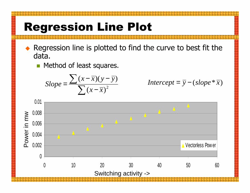
Regression Line Plot
� Regression line is plotted to find the curve to best fit the data.
� Method of least squares.
∑∑
−−−
=2)(
))((
xx
yyxxSlope )*( xslopeyIntercept −=
0
0.002
0.004
0.006
0.008
0.01
0 10 20 30 40 50 60
Vectorless Pow er
Switching activity ->
Pow
er in
mw

Correlation - vectorless vs absolutePower
Clock Power
0.00E+00
5.00E-04
1.00E-03
1.50E-03
2.00E-03
2.50E-03
2.00E-04
4.00E-04
6.00E-04
8.00E-04
1.00E-03
1.20E-03
1.40E-03
1.60E-03
1.80E-03
Register Power
Capture Pow er
Shif t Pow er
Vectorless Pow er
Power
(Flop)Toggling
Black Box Power
0.00E+00
5.00E-04
1.00E-03
1.50E-03
2.00E-03
2.50E-03
3.00E-03
3.50E-03
0 10 20 30 40 50 60
Combinational Power
0.00E+00
0 10 20 30 40 50 600.00E+00
0 10 20 30 40 50 60
0.00E+00
5.00E-04
1.00E-03
1.50E-03
2.00E-03
2.50E-03
3.00E-03
3.50E-03
4.00E-03
0 10 20 30 40 50 60
(Flop)Toggling

Correlation - vectorless vs absolutePower
TOTAL POWER
Power
(Flop)Toggling
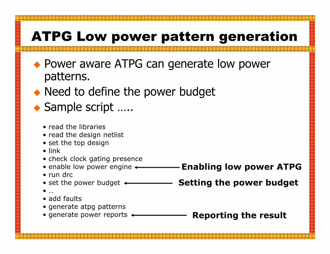
ATPG Low power pattern generation
� Power aware ATPG can generate low power patterns.
� Need to define the power budget
� Sample script …..
• read the libraries• read the libraries• read the design netlist• set the top design• link• check clock gating presence• enable low power engine• run drc• set the power budget• ..• add faults• generate atpg patterns• generate power reports
Enabling low power ATPG
Setting the power budget
Reporting the result

Low power vs std power vectors
Switching activity of Low Power Vs Standard power

Figures of merit …
1.08
22.48
0
5
10
15
20
25
Per
cent
age
switc
hing
Capture PowerCapture Power reduction - 20X
1.08
22.48
0
5
10
15
20
25
Per
cent
age
switc
hing
Capture PowerCapture Power reduction - 20X
91.66 91.63
20
40
60
80
100
Cov
erag
e
Test CoverageTest coverage - Same
91.66 91.63
20
40
60
80
100
Cov
erag
e
Test CoverageTest coverage - Same
0Low Power STD Power
0Low Power STD Power
0Low Power STD Power
0Low Power STD Power
60784
28296
0
10000
20000
30000
40000
50000
60000
70000
Num
ber
of P
atte
rns
Low Power STD Power
Pattern Count Pattern Inflation of 2X
60784
28296
0
10000
20000
30000
40000
50000
60000
70000
Num
ber
of P
atte
rns
Low Power STD Power
Pattern Count Pattern Inflation of 2X
36.02
18.8
0
5
10
15
20
25
30
35
40
run
time
(Hrs
)
Low Power STD Power
Run TimeRun time increase - 2X
36.02
18.8
0
5
10
15
20
25
30
35
40
run
time
(Hrs
)
Low Power STD Power
Run TimeRun time increase - 2X
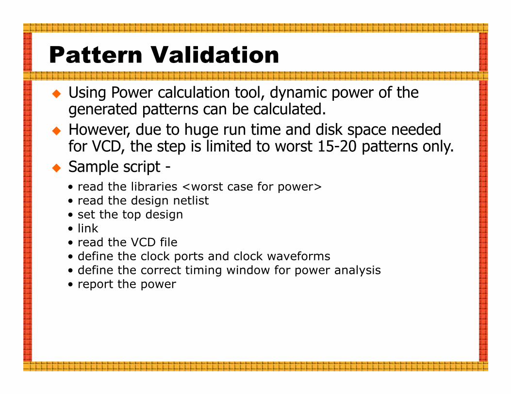
Pattern Validation
� Using Power calculation tool, dynamic power of the generated patterns can be calculated.
� However, due to huge run time and disk space needed for VCD, the step is limited to worst 15-20 patterns only.
� Sample script -• read the libraries <worst case for power>• read the design netlist• read the design netlist• set the top design• link• read the VCD file• define the clock ports and clock waveforms • define the correct timing window for power analysis• report the power
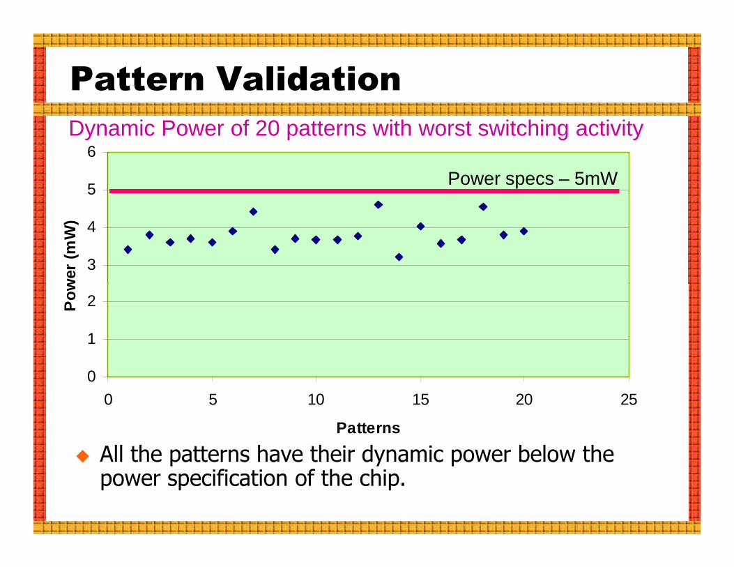
Pattern Validation
3
4
5
6
Po
wer
(m
W)
Power specs – 5mW
Dynamic Power of 20 patterns with worst switching activity
0
1
2
0 5 10 15 20 25
Patterns
Po
wer
(m
W)
� All the patterns have their dynamic power below the power specification of the chip.
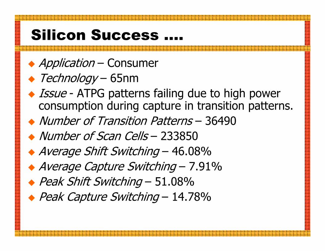
Silicon Success ….
� Application – Consumer
� Technology – 65nm
� Issue - ATPG patterns failing due to high power consumption during capture in transition patterns.
� Number of Transition Patterns – 36490� Number of Transition Patterns – 36490
� Number of Scan Cells – 233850
� Average Shift Switching – 46.08%
� Average Capture Switching – 7.91%
� Peak Shift Switching – 51.08%
� Peak Capture Switching – 14.78%
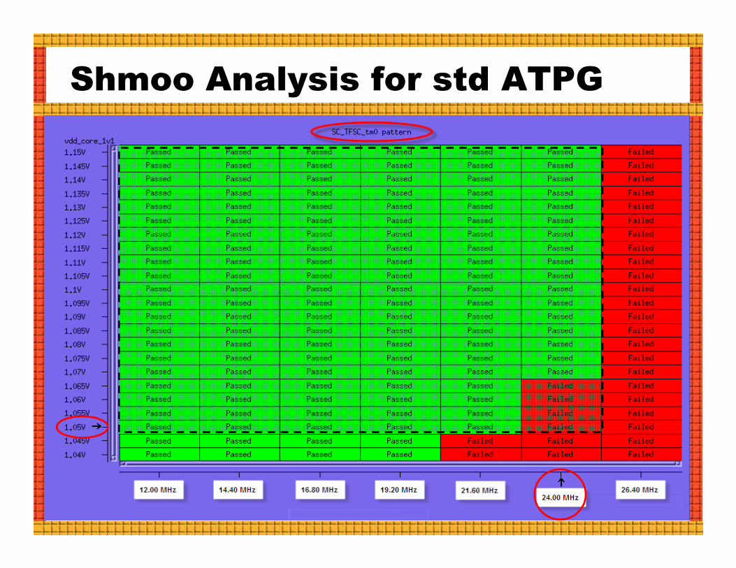
Shmoo Analysis for std ATPG
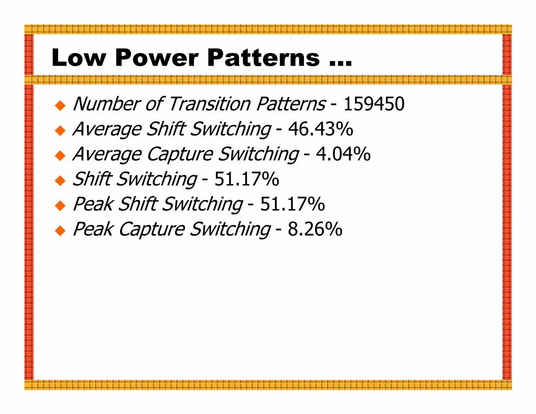
Low Power Patterns …
� Number of Transition Patterns - 159450
� Average Shift Switching - 46.43%
� Average Capture Switching - 4.04%
� Shift Switching - 51.17%
� Peak Shift Switching - 51.17%� Peak Shift Switching - 51.17%
� Peak Capture Switching - 8.26%

Shmoo for Low Power ATPG

Conclusion
� Power has become a challenge not only infunctional mode but also in test mode.
� The proposed flow, consisting of in-house andEDA tools gives an complete automated flow forlow power test methodology.
The insertion of level shifters, isolation logic and� The insertion of level shifters, isolation logic andtest control point insertion for scan signals is nowfully automated.
� Low Power ATPG flow generates low powerpatterns within the power specification of thedesign.
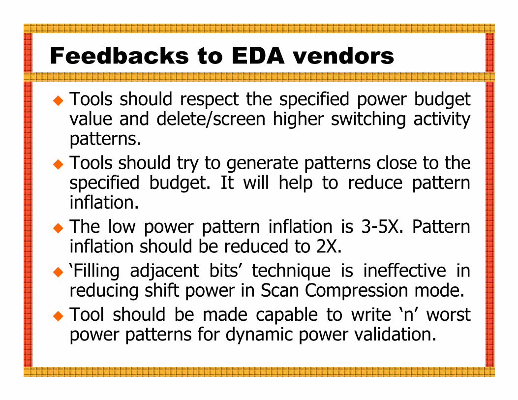
Feedbacks to EDA vendors
� Tools should respect the specified power budgetvalue and delete/screen higher switching activitypatterns.
� Tools should try to generate patterns close to thespecified budget. It will help to reduce patterninflation.inflation.
� The low power pattern inflation is 3-5X. Patterninflation should be reduced to 2X.
� ‘Filling adjacent bits’ technique is ineffective inreducing shift power in Scan Compression mode.
� Tool should be made capable to write ‘n’ worstpower patterns for dynamic power validation.


