

LTC6754
16754f
For more information www.linear.com/LTC6754
Typical applicaTion
FeaTures DescripTion
High Speed Rail-to-Rail Input Comparator with
LVDS Compatible Outputs
The LTC®6754 is a high speed rail-to-rail comparator with LVDS compatible outputs. The LTC6754 exhibits 1.8ns of propagation delay, only 1ns of dispersion (10mV to 125mV overdrive) and a toggle rate up to 890Mbps.
The LTC6754 has rail-to-rail inputs, and will operate from a 2.4V to 5.25V supply. For the QFN package, the LVDS output is operated with a separate supply, providing isola-tion between input and output circuitry, and allowing for logic level translation.
In shutdown mode, power is reduced from 13.4mA to under 1.1mA, and the comparator can wake up in 120ns.
The LTC6754 includes 4.5mV of hysteresis to minimize instability. For the QFN package, a separate pin is available to set the hysteresis from 0mV (off) up to 40mV. The QFN version also features output latching to provide the ability to quickly capture the state of the comparator.
The dispersion of only 1ns combined with excellent propagation delay of 1.8ns makes the device an excel-lent choice for timing critical applications. Similarly, the 890Mbps toggle rate and low jitter of 1.5psRMS (200mVP–P, 245.76MHz input) make the LTC6754 ideally suited for high frequency line driver and clock recovery circuits.L, LT, LTC, LTM, Linear Technology and the Linear logo are registered trademarks of Linear Technology Corporation. All other trademarks are the property of their respective owners.
applicaTions
n Low Propagation Delay: 1.8ns Typ. n Low Overdrive Dispersion: 1ns Typ.
(10mV to 125mV Overdrive) n High Toggle Rate: 890Mbps Typ. n LVDS Compatible Output Stage n Rail-to-Rail Inputs Extend Beyond Both Rails n Low Quiescent Current: 13.4mA n Supply Range: 2.4V to 5.25V n Features within the LTC6754 Family:
n Separate Input and Output Supplies n Shutdown Pin for Reduced Power n Output Latch and Adjustable Hysteresis n SC70 and 3mm × 3mm QFN Packages
n Clock and Data Recovery n Level Translation n High Speed Data Acquisition Systems n Window Comparators n High Speed Line Receivers n Time Domain Reflectometry n Time of Flight Measurements n Cable Drivers
20ns/DIV
Q – Q100mV/DIV
0mV
+IN, –IN200mV/DIV
700mV
6754 F16
–INQ – Q +IN
High Speed Differential Line Receiver and LVDS Translator with Excellent Common Mode Rejection
VCCI
VCCO
–
+ Q
100Ω
Q
6754 T01a
SMALL DIFFERENTIAL SIGNAL WITH LARGE COMMON MODE COMPONENT
VEE
+IN
–INLTC6754
LTC6754
26754f
For more information www.linear.com/LTC6754
absoluTe MaxiMuM raTings
Total Input Supply Voltage (VEE to VCCI) ..................5.5VTotal Output Supply Voltage (VEE to VCCO)...............5.5VInput Voltage
–IN, +IN, LE/HYST, SHDN .......VEE – 0.3V, VCCI + 0.3VInput Current
–IN, +IN, LE/HYST, SHDN (Note 2) .................. ±10mA Output Current(Q, Q) ........................................... ±20mA
(Note 1)
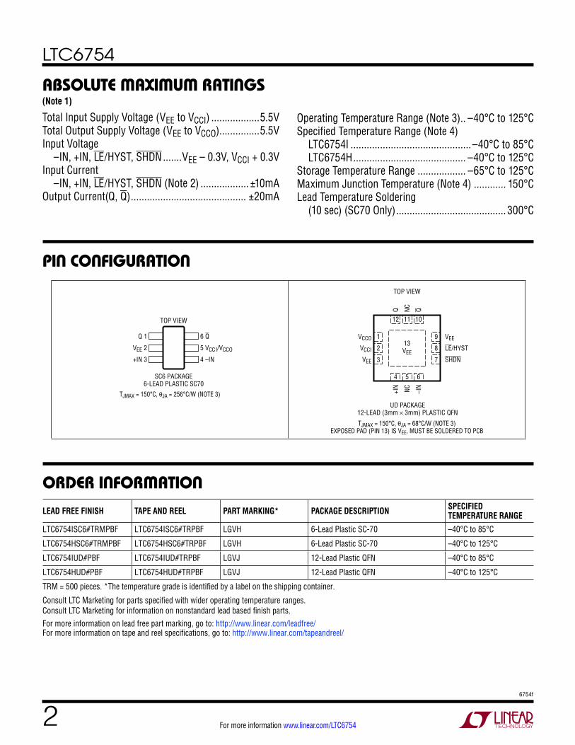
Q 1
VEE 2
+IN 3
6 Q
5 VCCI/VCCO
4 –IN
TOP VIEW
SC6 PACKAGE6-LEAD PLASTIC SC70
TJMAX = 150°C, θJA = 256°C/W (NOTE 3)
12 11 10
4 5 6
TOP VIEW
13VEE
UD PACKAGE12-LEAD (3mm × 3mm) PLASTIC QFN
7
8
9
3
2
1VCCO
VCCI
VEE
VEE
LE/HYST
SHDN
Q NC Q
+IN NC –IN
TJMAX = 150°C, θJA = 68°C/W (NOTE 3)
EXPOSED PAD (PIN 13) IS VEE, MUST BE SOLDERED TO PCB
orDer inForMaTion
pin conFiguraTion
LEAD FREE FINISH TAPE AND REEL PART MARKING* PACKAGE DESCRIPTION SPECIFIED TEMPERATURE RANGE
LTC6754ISC6#TRMPBF LTC6754ISC6#TRPBF LGVH 6-Lead Plastic SC-70 –40°C to 85°C
LTC6754HSC6#TRMPBF LTC6754HSC6#TRPBF LGVH 6-Lead Plastic SC-70 –40°C to 125°C
LTC6754IUD#PBF LTC6754IUD#TRPBF LGVJ 12-Lead Plastic QFN –40°C to 85°C
LTC6754HUD#PBF LTC6754HUD#TRPBF LGVJ 12-Lead Plastic QFN –40°C to 125°C
TRM = 500 pieces. *The temperature grade is identified by a label on the shipping container.
Consult LTC Marketing for parts specified with wider operating temperature ranges. Consult LTC Marketing for information on nonstandard lead based finish parts.For more information on lead free part marking, go to: http://www.linear.com/leadfree/ For more information on tape and reel specifications, go to: http://www.linear.com/tapeandreel/
Operating Temperature Range (Note 3) .. –40°C to 125°CSpecified Temperature Range (Note 4)
LTC6754I .............................................–40°C to 85°C LTC6754H .......................................... –40°C to 125°C
Storage Temperature Range .................. –65°C to 125°CMaximum Junction Temperature (Note 4) ............ 150°CLead Temperature Soldering
(10 sec) (SC70 Only) ......................................... 300°C

LTC6754
36754f
For more information www.linear.com/LTC6754
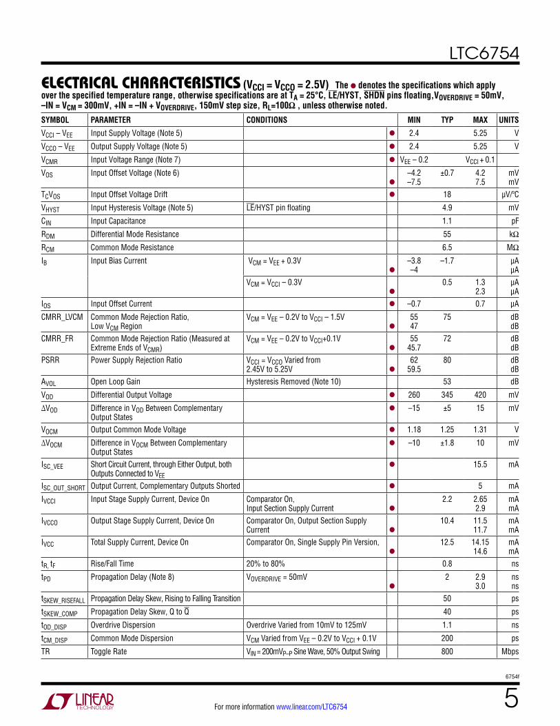
SYMBOL PARAMETER CONDITIONS MIN TYP MAX UNITS
VCCI–VEE Input Supply Voltage (Note 5) l 2.4 5.25 V
VCCO–VEE Output Supply Voltage (Note 5) l 2.4 5.25 V
VCMR Input Voltage Range (Note 7) l VEE – 0.2 VCCI + 0.1
VOS Input Offset Voltage (Note 6)
l
–4 –8.5
±0.75 4 8.5
mV mV
TCVOS Input Offset Voltage Drift l 18 µV/ºC
VHYST Input Hysteresis Voltage (Note 5) LE/HYST pin floating 4.5 mV
CIN Input Capacitance 1.1 pF
RDM Differential Mode Resistance 55 kΩ
RCM Common Mode Resistance 6.5 MΩ
IB Input Bias Current VCM = VEE + 0.3V
l
–3.8 –4
–1.8 μA µA
VCM = VCCI – 0.3V
l
0.6 1.5 2.5
µA µA
IOS Input Offset Current l –0.7 0.7 μA
CMRR_LVCM Common Mode Rejection Ratio, Low VCM Region
VCM = VEE – 0.2V to VCCI – 1.5V
l
58 53
77 dB dB
CMRR_FR Common Mode Rejection Ratio (Measured at Extreme Ends of VCMR)
VCM = VEE – 0.2V to VCCI+0.1V
l
60 50
76.5 dB dB
PSRR Power Supply Rejection Ratio VCCI = VCCO Varied from 2.45V to 5.25V
l
62 59.5
80 dB dB
AVOL Open Loop Gain Hysteresis Removed (Note 10) 53 dB
VOD Differential Output Voltage l 260 362 420 mV
ΔVOD Difference in VOD Between Complementary Output States
l –15 ±5 15 mV
VOCM Output Common Mode Voltage l 1.18 1.26 1.31 V
ΔVOCM Difference in VOD Between Complementary Output States
l –10 ±1.8 10 mV
ISC_VEE Short Circuit Current, through Either Output, both Outputs Connected to VEE
l 20 mA
ISC_OUT_SHORT Output Current, Complementary Outputs Shorted l 5 mA
IVCCI Input Stage Supply Current, Device On Comparator On, Input Section Supply Current
l
2.4 2.9 3
mA mA
IVCCO Output Stage Supply Current, Device On Comparator On, Output Section Supply Current
l
11 11.8 12.5
mA mA
IVCC Total Supply Current, Device On Comparator On, Single Supply Pin Version,
l
13.4 14.7 15.5
mA mA
tR, tF Rise/Fall Time 20% to 80% 0.77 ns
tPD Propagation Delay (Note 8) VOVERDRIVE = 50mV
l
1.8 2.8 2.9
ns ns
tSKEW_RISEFALL Propagation Delay Skew, Rising to Falling Transition 40 ps
tSKEW_COMP Propagation Delay Skew, Q to Q 50 ps
tOD_DISP Overdrive Dispersion Overdrive Varied from 10mV to 125mV 1 ns
tCM_DISP Common Mode dispersion VCM Varied from VEE – 0.2V to VCCI + 0.1V 200 ps
TR Toggle Rate VIN = 200mVP–P Sine Wave, 50% Output Swing 890 Mbps
The l denotes the specifications which apply over the specified temperature range, otherwise specifications are at TA = 25°C, LE/HYST, SHDN pins floating, VOVERDRIVE = 50mV, –IN = VCM = 300mV, +IN = –IN + VOVERDRIVE, 150mV step size, RL=100Ω , unless otherwise noted.
elecTrical characTerisTics (VCCI = VCCO = 5.0V)

LTC6754
46754f
For more information www.linear.com/LTC6754
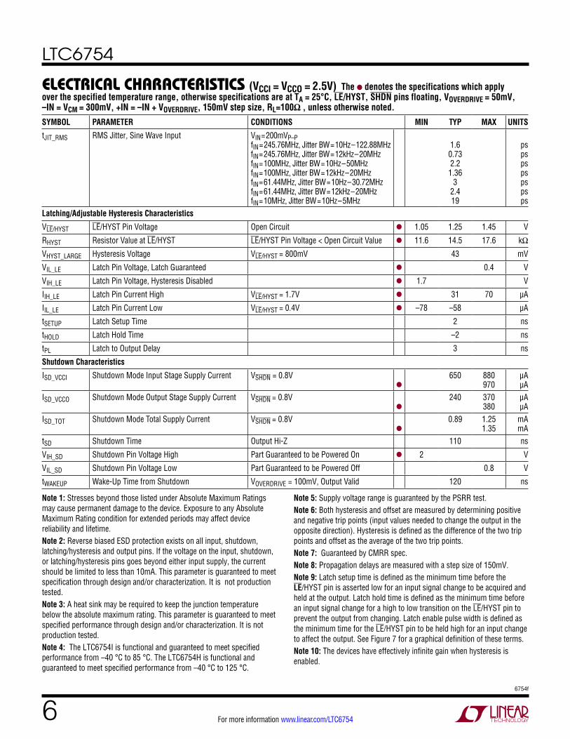
SYMBOL PARAMETER CONDITIONS MIN TYP MAX UNITS
tJIT_RMS RMS Jitter, Sine Wave Input VIN = 200mVP–P fIN = 245.76MHz, Jitter BW = 10Hz – 122.88MHz fIN = 245.76MHz, Jitter BW = 12kHz – 20MHz fIN = 100MHz, Jitter BW = 10Hz – 50MHz fIN = 100MHz, Jitter BW = 12kHz – 20MHz fIN = 61.44MHz, Jitter BW = 10Hz – 30.72MHz fIN = 61.44MHz, Jitter BW = 12kHz – 20MHz fIN = 10MHz, Jitter BW = 10Hz – 5MHz
1.53 0.7 2.2
1.34 2.93 2.37 20
ps ps ps ps ps ps ps
Latching/Adjustable Hysteresis Characteristics
VLE/HYST LE/HYST Pin Voltage Open Circuit l 1.05 1.25 1.45 V
RHYST Resistor Value at LE/HYST LE/HYST Pin Voltage < Open Circuit Value l 11.6 14.5 17.6 kΩ
VHYST_LARGE Hysteresis Voltage VLE/HYST = 800mV 40 mV
VIL_LE Latch Pin Voltage, Latch Guaranteed l 0.4 V
VIH_LE Latch Pin Voltage, Hysteresis Disabled l 1.7 V
IIH_LE Latch Pin Current High VLE/HYST = 1.7V l 31 70 µA
IIL_LE Latch Pin Current Low VLE/HYST = 0.4V l –75 –59 µA
tSETUP Latch Setup Time 2 ns
tHOLD Latch Hold Time –2 ns
tPL Latch to Output Delay 3 ns
Shutdown Characteristics
ISD_VCCI Shutdown Mode Input Stage Supply Current VSHDN = 0.8V
l
0.78 1.07 1.14
mA mA
ISD_VCCO Shutdown Mode Output Stage Supply Current VSHDN = 0.8V
l
270 410 430
μA µA
ISD_TOT Shutdown Mode Total Supply Current VSHDN = 0.8V
l
1.05 1.48 1.57
mA mA
tSD Shutdown Time Output Hi-Z 110 ns
VIH_SD Shutdown Pin Voltage High Part Guaranteed to be Powered On l 2 V
VIL_SD Shutdown Pin Voltage Low Part Guaranteed to be Powered Off 0.8 V
tWAKEUP Wake-Up Time from Shutdown VOVERDRIVE = 100mV, Output Valid 120 ns
The l denotes the specifications which apply over the specified temperature range, otherwise specifications are at TA = 25°C, LE/HYST, SHDN pins floating, VOVERDRIVE = 50mV, –IN = VCM = 300mV, +IN = –IN + VOVERDRIVE, 150mV step size, RL=100Ω , unless otherwise noted.
elecTrical characTerisTics (VCCI = VCCO = 5.0V)
LTC6754
56754f
For more information www.linear.com/LTC6754
elecTrical characTerisTics (VCCI = VCCO = 2.5V)
SYMBOL PARAMETER CONDITIONS MIN TYP MAX UNITS
VCCI – VEE Input Supply Voltage (Note 5) l 2.4 5.25 V
VCCO – VEE Output Supply Voltage (Note 5) l 2.4 5.25 V
VCMR Input Voltage Range (Note 7) l VEE – 0.2 VCCI + 0.1
VOS Input Offset Voltage (Note 6)
l
–4.2 –7.5
±0.7 4.2 7.5
mV mV
TCVOS Input Offset Voltage Drift l 18 µV/ºC
VHYST Input Hysteresis Voltage (Note 5) LE/HYST pin floating 4.9 mV
CIN Input Capacitance 1.1 pF
RDM Differential Mode Resistance 55 kΩ
RCM Common Mode Resistance 6.5 MΩ
IB Input Bias Current VCM = VEE + 0.3V
l
–3.8 –4
–1.7 µA μA
VCM = VCCI – 0.3V
l
0.5 1.3 2.3
µA μA
IOS Input Offset Current l –0.7 0.7 μA
CMRR_LVCM Common Mode Rejection Ratio, Low VCM Region
VCM = VEE – 0.2V to VCCI – 1.5V
l
55 47
75 dB dB
CMRR_FR Common Mode Rejection Ratio (Measured at Extreme Ends of VCMR)
VCM = VEE – 0.2V to VCCI+0.1V
l
55 45.7
72 dB dB
PSRR Power Supply Rejection Ratio VCCI = VCCO Varied from 2.45V to 5.25V
l
62 59.5
80 dB dB
AVOL Open Loop Gain Hysteresis Removed (Note 10) 53 dB
VOD Differential Output Voltage l 260 345 420 mV
ΔVOD Difference in VOD Between Complementary Output States
l –15 ±5 15 mV
VOCM Output Common Mode Voltage l 1.18 1.25 1.31 V
ΔVOCM Difference in VOCM Between Complementary Output States
l –10 ±1.8 10 mV
ISC_VEE Short Circuit Current, through Either Output, both Outputs Connected to VEE
l 15.5 mA
ISC_OUT_SHORT Output Current, Complementary Outputs Shorted l 5 mA
IVCCI Input Stage Supply Current, Device On Comparator On, Input Section Supply Current
l
2.2 2.65 2.9
mA mA
IVCCO Output Stage Supply Current, Device On Comparator On, Output Section Supply Current
l
10.4 11.5 11.7
mA mA
IVCC Total Supply Current, Device On Comparator On, Single Supply Pin Version,
l
12.5 14.15 14.6
mA mA
tR, tF Rise/Fall Time 20% to 80% 0.8 ns
tPD Propagation Delay (Note 8) VOVERDRIVE = 50mV
l
2 2.9 3.0
ns ns
tSKEW_RISEFALL Propagation Delay Skew, Rising to Falling Transition 50 ps
tSKEW_COMP Propagation Delay Skew, Q to Q 40 ps
tOD_DISP Overdrive Dispersion Overdrive Varied from 10mV to 125mV 1.1 ns
tCM_DISP Common Mode Dispersion VCM Varied from VEE – 0.2V to VCCI + 0.1V 200 ps
TR Toggle Rate VIN = 200mVP–P Sine Wave, 50% Output Swing 800 Mbps
The l denotes the specifications which apply over the specified temperature range, otherwise specifications are at TA = 25°C, LE/HYST, SHDN pins floating,VOVERDRIVE = 50mV, –IN = VCM = 300mV, +IN = –IN + VOVERDRIVE, 150mV step size, RL=100Ω , unless otherwise noted.
LTC6754
66754f
For more information www.linear.com/LTC6754
SYMBOL PARAMETER CONDITIONS MIN TYP MAX UNITS
tJIT_RMS RMS Jitter, Sine Wave Input VIN = 200mVP–P fIN = 245.76MHz, Jitter BW = 10Hz – 122.88MHz fIN = 245.76MHz, Jitter BW = 12kHz – 20MHz fIN = 100MHz, Jitter BW = 10Hz – 50MHz fIN = 100MHz, Jitter BW = 12kHz – 20MHz fIN = 61.44MHz, Jitter BW = 10Hz – 30.72MHz fIN = 61.44MHz, Jitter BW = 12kHz – 20MHz fIN = 10MHz, Jitter BW = 10Hz – 5MHz
1.6
0.73 2.2
1.36 3
2.4 19
ps ps ps ps ps ps ps
Latching/Adjustable Hysteresis Characteristics
VLE/HYST LE/HYST Pin Voltage Open Circuit l 1.05 1.25 1.45 V
RHYST Resistor Value at LE/HYST LE/HYST Pin Voltage < Open Circuit Value l 11.6 14.5 17.6 kΩ
VHYST_LARGE Hysteresis Voltage VLE/HYST = 800mV 43 mV
VIL_LE Latch Pin Voltage, Latch Guaranteed l 0.4 V
VIH_LE Latch Pin Voltage, Hysteresis Disabled l 1.7 V
IIH_LE Latch Pin Current High VLE/HYST = 1.7V l 31 70 µA
IIL_LE Latch Pin Current Low VLE/HYST = 0.4V l –78 –58 µA
tSETUP Latch Setup Time 2 ns
tHOLD Latch Hold Time –2 ns
tPL Latch to Output Delay 3 ns
Shutdown Characteristics
ISD_VCCI Shutdown Mode Input Stage Supply Current VSHDN = 0.8V
l
650 880 970
μA µA
ISD_VCCO Shutdown Mode Output Stage Supply Current VSHDN = 0.8V
l
240 370 380
μA µA
ISD_TOT Shutdown Mode Total Supply Current VSHDN = 0.8V
l
0.89 1.25 1.35
mA mA
tSD Shutdown Time Output Hi-Z 110 ns
VIH_SD Shutdown Pin Voltage High Part Guaranteed to be Powered On l 2 V
VIL_SD Shutdown Pin Voltage Low Part Guaranteed to be Powered Off 0.8 V
tWAKEUP Wake-Up Time from Shutdown VOVERDRIVE = 100mV, Output Valid 120 ns
The l denotes the specifications which apply over the specified temperature range, otherwise specifications are at TA = 25°C, LE/HYST, SHDN pins floating, VOVERDRIVE = 50mV, –IN = VCM = 300mV, +IN = –IN + VOVERDRIVE, 150mV step size, RL=100Ω , unless otherwise noted.
elecTrical characTerisTics (VCCI = VCCO = 2.5V)
Note 1: Stresses beyond those listed under Absolute Maximum Ratings may cause permanent damage to the device. Exposure to any Absolute Maximum Rating condition for extended periods may affect device reliability and lifetime. Note 2: Reverse biased ESD protection exists on all input, shutdown, latching/hysteresis and output pins. If the voltage on the input, shutdown, or latching/hysteresis pins goes beyond either input supply, the current should be limited to less than 10mA. This parameter is guaranteed to meet specification through design and/or characterization. It is not production tested.Note 3: A heat sink may be required to keep the junction temperature below the absolute maximum rating. This parameter is guaranteed to meet specified performance through design and/or characterization. It is not production tested.Note 4: The LTC6754I is functional and guaranteed to meet specified performance from –40 °C to 85 °C. The LTC6754H is functional and guaranteed to meet specified performance from –40 °C to 125 °C.
Note 5: Supply voltage range is guaranteed by the PSRR test.Note 6: Both hysteresis and offset are measured by determining positive and negative trip points (input values needed to change the output in the opposite direction). Hysteresis is defined as the difference of the two trip points and offset as the average of the two trip points.Note 7: Guaranteed by CMRR spec.Note 8: Propagation delays are measured with a step size of 150mV.Note 9: Latch setup time is defined as the minimum time before the LE/HYST pin is asserted low for an input signal change to be acquired and held at the output. Latch hold time is defined as the minimum time before an input signal change for a high to low transition on the LE/HYST pin to prevent the output from changing. Latch enable pulse width is defined as the minimum time for the LE/HYST pin to be held high for an input change to affect the output. See Figure 7 for a graphical definition of these terms. Note 10: The devices have effectively infinite gain when hysteresis is enabled.
LTC6754
76754f
For more information www.linear.com/LTC6754
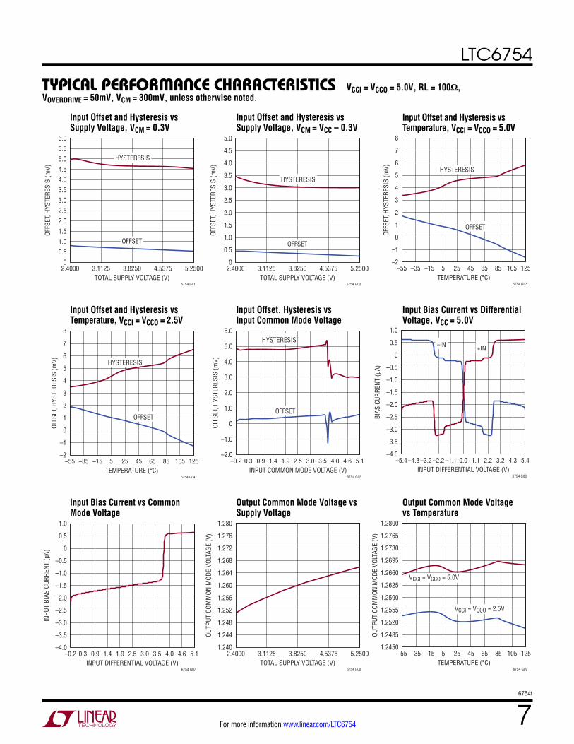
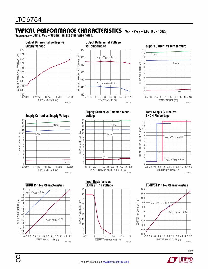
Typical perForMance characTerisTics
Input Offset and Hysteresis vs Temperature, VCCI = VCCO = 2.5V
Input Offset, Hysteresis vs Input Common Mode Voltage
Input Bias Current vs Differential Voltage, VCC = 5.0V
Input Bias Current vs Common Mode Voltage
Output Common Mode Voltage vs Supply Voltage
Output Common Mode Voltage vs Temperature
Input Offset and Hysteresis vs Supply Voltage, VCM = 0.3V
Input Offset and Hysteresis vs Supply Voltage, VCM = VCC – 0.3V
Input Offset and Hysteresis vs Temperature, VCCI = VCCO = 5.0V
VCCI = VCCO = 5.0V, RL = 100Ω, VOVERDRIVE = 50mV, VCM = 300mV, unless otherwise noted.
TOTAL SUPPLY VOLTAGE (V)2.4000 3.1125 3.8250 4.5375 5.25000
0.5
1.0
1.5
2.0
2.5
3.0
3.5
4.0
4.5
5.0
5.5
6.0
OFFS
ET, H
YSTE
RESI
S (m
V)
Supply Voltage, VCM = 0.3VInput Offset and Hysteresis vs
6754 G01
HYSTERESIS
OFFSET
HYSTERESIS
OFFSET
TOTAL SUPPLY VOLTAGE (V)2.4000 3.1125 3.8250 4.5375 5.25000
0.5
1.0
1.5
2.0
2.5
3.0
3.5
4.0
4.5
5.0
OFFS
ET, H
YSTE
RESI
S (m
V)
Supply Voltage, VCM = VCCI– 0.3VInput Offset and Hysteresis vs
6754 G02
HYSTERESIS
OFFSET
TEMPERATURE (°C)–55 –35 –15 5 25 45 65 85 105 125
–2
–1
0
1
2
3
4
5
6
7
8
OFFS
ET, H
YSTE
RESI
S (m
V)
6754 G03
HYSTERESIS
OFFSET
TEMPERATURE (°C)–55 –35 –15 5 25 45 65 85 105 125
–2
–1
0
1
2
3
4
5
6
7
8
OFFS
ET, H
YSTE
RESI
S (m
V)
6754 G04
HYSTERESIS
OFFSET
INPUT COMMON MODE VOLTAGE (V)–0.2 0.3 0.9 1.4 1.9 2.5 3.0 3.5 4.0 4.6 5.1
–2.0
–1.0
0
1.0
2.0
3.0
4.0
5.0
6.0
OFFS
ET, H
YSTE
RESI
S (m
V)
Input Common Mode VoltageInput Offset, Hysteresis vs
6754 G05
TOTAL SUPPLY VOLTAGE (V)2.4000 3.1125 3.8250 4.5375 5.2500
1.240
1.244
1.248
1.252
1.256
1.260
1.264
1.268
1.272
1.276
1.280
OUTP
UT C
OMM
ON M
ODE
VOLT
AGE
(V)
Supply VoltageOutput Common Mode Voltage vs
6754 G08
VCCI = VCCO = 5.0V
VCCI = VCCO = 2.5V
TEMPERATURE (°C)–55 –35 –15 5 25 45 65 85 105 125
1.2450
1.2485
1.2520
1.2555
1.2590
1.2625
1.2660
1.2695
1.2730
1.2765
1.2800
OUTP
UT C
OMM
ON M
ODE
VOLT
AGE
(V)
6754 G09
+IN–IN
INPUT DIFFERENTIAL VOLTAGE (V)–5.4 –4.3 –3.2 –2.2 –1.1 0.0 1.1 2.2 3.2 4.3 5.4
–4.0
–3.5
–3.0
–2.5
–2.0
–1.5
–1.0
–0.5
0
0.5
1.0
BIAS
CUR
RENT
(µA)
6754 G06
INPUT DIFFERENTIAL VOLTAGE (V)–0.2 0.3 0.9 1.4 1.9 2.5 3.0 3.5 4.0 4.6 5.1
–4.0
–3.5
–3.0
–2.5
–2.0
–1.5
–1.0
–0.5
0
0.5
1.0
INPU
T BI
AS C
URRE
NT (µ
A)
6754 G07
LTC6754
86754f
For more information www.linear.com/LTC6754
Supply Current vs Supply VoltageSupply Current vs Common Mode Voltage
Total Supply Current vs SHDN Pin Voltage
SHDN Pin I–V CharacteristicsInput Hysteresis vs LE/HYST Pin Voltage LE/HYST Pin I–V Characteristics
Output Differential Voltage vs Supply Voltage
Output Differential Voltage vs Temperature Supply Current vs Temperature
VCCI = VCCO = 5.0V, RL = 100Ω, VOVERDRIVE = 50mV, VCM = 300mV, unless otherwise noted.Typical perForMance characTerisTics
SUPPLY VOLTAGE (V)2.4000 3.1125 3.8250 4.5375 5.2500
340
343
346
349
352
355
358
361
364
367
370
OUTP
UT D
IFFE
RENT
IAL
VOLT
AGE
(mV)
Supply VoltageOutput Differential Voltage vs
6754 G10
VCCI = VCCO = 5V
VCCI = VCCO = 2.5V
TEMPERATURE (°C)–55 –35 –15 5 25 45 65 85 105 125
340
345
350
355
360
365
370
OUTP
UT D
IFFE
RENT
IAL
VOLT
AGE
(mV)
vs TemperatureOutput Differential Voltage
6754 G11
IVCCI
IVCCO
ITOTAL
TEMPERATURE (°C)–55 –35 –15 5 25 45 65 85 105 125
123456789
1011121314
SUPP
LY C
URRE
NT (m
A)
Supply Current vs Temperature
6754 G12
IVCCI
IVCCO
ITOTAL
SUPPLY VOLTAGE (V)2.4000 3.1125 3.8250 4.5375 5.2500123456789
1011121314
SUPP
LY C
URRE
NT (m
A)
Supply Current vs Supply Voltage
6754 G13
IVCCI
IVCCO
ITOTAL
INPUT COMMON MODE VOLTAGE (V)–0.2 0.3 0.9 1.4 1.9 2.5 3.0 3.5 4.0 4.6 5.1123456789
1011121314
SUPP
LY C
URRE
NT (m
A)
VoltageSupply Current vs Common Mode
6754 G14
VCCI = VCCO = 5.0V
VCCI = VCCO = 2.5V
SHDN PIN VOLTAGE (V)–0.3 0.3 0.8 1.4 1.9 2.5 3.1 3.6 4.2 4.7 5.30123456789
1011121314
TOTA
L SU
PPLY
CUR
RENT
(mA)
6754 G15
VCCI = VCCO = 5.0V
VCCI = VCCO = 2.5V
SHDN PIN VOLTAGE (V)–0.3 0.3 0.8 1.4 1.9 2.5 3.1 3.6 4.2 4.7 5.3
–15–14–13–12–11–10–9–8–7–6–5–4–3–2–1
01
SHDN
PIN
CUR
RENT
(µA)
SHDN Pin I–V Characteristics
6754 G16LE/HYST PIN VOLTAGE (V)
0.75 1 1.25 1.50 1.75 20
5
10
15
20
25
30
35
40
45
INPU
T HY
STER
ESIS
(mV)
LE/HYST Pin VoltageInput Hysteresis vs
6754 G17
VCCI = VCCO = 2.5V
VCCI = VCCO = 5.0V
LE/HYST PIN VOLTAGE (V)–0.3 0.3 0.8 1.4 1.9 2.5 3.1 3.6 4.2 4.7 5.3
–120
–90
–60
–30
0
30
60
90
120
150
180
LE/HYS
T PI
N CU
RREN
T (µ
A)
6754 G18
LTC6754
96754f
For more information www.linear.com/LTC6754
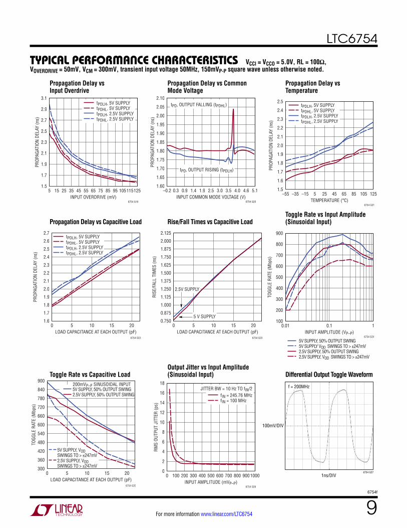
Typical perForMance characTerisTics
Propagation Delay vs Capacitive Load Rise/Fall Times vs Capacitive LoadToggle Rate vs Input Amplitude (Sinusoidal Input)
Toggle Rate vs Capacitive LoadOutput Jitter vs Input Amplitude (Sinusoidal Input) Differential Output Toggle Waveform
Propagation Delay vs Input Overdrive
Propagation Delay vs Common Mode Voltage
Propagation Delay vs Temperature
VCCI = VCCO = 5.0V, RL = 100Ω, VOVERDRIVE = 50mV, VCM = 300mV, transient input voltage 50MHz, 150mVP-P square wave unless otherwise noted.
INPUT OVERDRIVE (mV)5 15 25 35 45 55 65 75 85 95 105115125
1.5
1.7
1.9
2.1
2.3
2.5
2.7
2.9
3.1
PROP
AGAT
ION
DELA
Y (n
s)
Input OverdrivePropagation Delay vs
6754 G19
tPDLH, 5V SUPPLYtPDHL, 5V SUPPLYtPDLH, 2.5V SUPPLYtPDHL, 2.5V SUPPLY
tPD, OUTPUT FALLING (tPDHL)
tPD, OUTPUT RISING (tPDLH)
INPUT COMMON MODE VOLTAGE (V)–0.2 0.3 0.9 1.4 1.9 2.5 3.0 3.5 4.0 4.6 5.1
1.60
1.65
1.70
1.75
1.80
1.85
1.90
1.95
2.00
2.05
2.10
PROP
AGAT
ION
DELA
Y (n
s)
Mode VoltagePropagation Delay vs Common
6754 G20
5V SUPPLY, 50% OUTPUT SWING5V SUPPLY VOD SWINGS TO > ±247mV2.5V SUPPLY, 50% OUTPUT SWING2.5V SUPPLY, VOD SWINGS TO > ±247mV
INPUT AMPLITUDE (VP–P)0.01 0.1 1
100
200
300
400
500
600
700
800
900
TOGG
LE R
ATE
(Mbp
s)
6754 G24
1ns/DIV
100mV/DIV
6754 G27
f = 200MHz
tPDLH, 5V SUPPLYtPDHL, 5V SUPPLYtPDLH, 2.5V SUPPLYtPDHL, 2.5V SUPPLY
TEMPERATURE (°C)–55 –35 –15 5 25 45 65 85 105 125
1.5
1.6
1.7
1.8
1.9
2.0
2.1
2.2
2.3
2.4
2.5
PROP
AGAT
ION
DELA
Y (n
s)
6754 G21
tPDLH, 5V SUPPLYtPDHL, 5V SUPPLYtPDLH, 2.5V SUPPLYtPDHL, 2.5V SUPPLY
LOAD CAPACITANCE AT EACH OUTPUT (pF)0 5 10 15 20
1.6
1.7
1.8
1.9
2.0
2.1
2.2
2.3
2.4
2.5
2.6
2.7
PROP
AGAT
ION
DELA
Y (n
s)
6754 G22
2.5V SUPPLY
LOAD CAPACITANCE AT EACH OUTPUT (pF)0 5 10 15 20
0.750
0.875
1.000
1.125
1.250
1.375
1.500
1.625
1.750
1.875
2.000
2.125
RISE
/FAL
L TI
MES
(ns)
6754 G23
5 V SUPPLY
5V SUPPLY, VOD SWINGS TO > ±247mV
5V SUPPLY, 50% OUTPUT SWING2.5V SUPPLY, 50% OUTPUT SWING
2.5V SUPPLY, VODSWINGS TO > ±247mV
LOAD CAPACITANCE AT EACH OUTPUT (pF)0 5 10 15 20
300
360
420
480
540
600
660
720
780
840
900
TOGG
LE R
ATE
(Mbp
s)
6754 G25
200mVP–P SINUSOIDAL INPUTJITTER BW = 10 Hz TO fIN/2
fIN = 245.76 MHzfIN = 100 MHz
INPUT AMPLITUDE (mVP–P)0 100 200 300 400 500 600 700 800 900 1000
0
2
4
6
8
10
12
14
16
18
RMS
OUTP
UT J
ITTE
R (p
s)
6754 G26
LTC6754
106754f
For more information www.linear.com/LTC6754
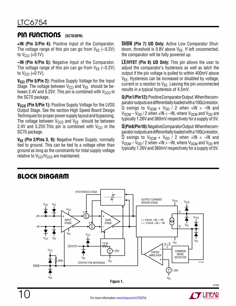
pin FuncTions+IN (Pin 3/Pin 4): Positive Input of the Comparator. The voltage range of this pin can go from VEE (–0.2V) to VCCI (+0.1V).
–IN (Pin 4/Pin 5): Negative Input of the Comparator. The voltage range of this pin can go from VEE (–0.2V) to VCCI (+0.1V).
VCCI (Pin 5/Pin 2): Positive Supply Voltage for the Input Stage. The voltage between VCCI and VEE should be be-tween 2.4V and 5.25V. This pin is combined with VCCO in the SC70 package.
VCCO (Pin 5/Pin 1): Positive Supply Voltage for the LVDS Output Stage. See the section High Speed Board Design Techniques for proper power supply layout and bypassing. The voltage between VCCO and VEE should be between 2.4V and 5.25V.This pin is combined with VCCI in the SC70 package.
VEE (Pin 2/Pins 3, 9): Negative Power Supply, normally tied to ground. This can be tied to a voltage other than ground as long as the constraints for total supply voltage relative to VCCI/VCCO are maintained.
SHDN (Pin 7) UD Only: Active Low Comparator Shut-down, threshold is 0.8V above VEE. If left unconnected, the comparator will be fully powered up.
LE/HYST (Pin 8) UD Only: This pin allows the user to adjust the comparator’s hysteresis as well as latch the output if the pin voltage is pulled to within 400mV above VEE. Hysteresis can be increased or disabled by voltage, current or a resistor to VEE. Leaving the pin unconnected results in a typical hysteresis of 4.5mV.
Q (Pin 1/Pin 12): Positive Comparator Output. When the com-parator outputs are differentially loaded with a 100Ω resistor, Q swings to VOCM + VOD / 2 when +IN > –IN and VOCM – VOD / 2 when +IN < –IN, where VOCM and VOD are typically 1.26V and 360mV respectively for a supply of 5V.
Q (Pin 6/Pin 10): Negative Comparator Output. When the com-parator outputs are differentially loaded with a 100Ω resistor, Q swings to VOCM + VOD / 2 when +IN < –IN and VOCM – VOD / 2 when +IN > –IN, where VOCM and VOD are typically 1.26V and 360mV respectively for a supply of 5V.
block DiagraM
VCCI
VCCI
VEE
VEE
6754 BD
VEE
VCCI
VEEVEE
–IN
VCCI VEE
VCCI
+IN
–
+INPUTSTAGE
HYSTERESIS STAGE
–
+GAIN
STAGEQ
Q
LE/HYST
SHDNLE/HYST PIN INTERFACE
14.5k
1.25V
350k
+
+
+–
+–
OUTPUT CURRENTDRIVER STAGE
1.26V
–
+
COMMONMODE
DETECTOR
I = 3.6mA, +IN < –INI = –3.6mA, +IN > –IN
VEE
VEE
VEE
VCCOVCCO
VEE
VCCO
ERRORAMPLIFIER
Q + Q2
Figure 1.
(SC70/QFN)
LTC6754
116754f
For more information www.linear.com/LTC6754
Circuit Description
The block diagram of the LTC6754 is shown in Figure 1. There are differential inputs (+IN, –IN), a negative power supply (VEE), two positive supply pins: VCCI for the input stage and VCCO for the output stage, two output pins (Q and Q), a pin for latching and adjusting hysteresis (LE/HYST), and a pin to put the device in a low power mode (SHDN). The signal path consists of a rail-to-rail input stage, an intermediate gain stage and an output driver stage to an output stage that sources or sinks 3.6mA between the two output pins, depending on the polarity of the differential input (+IN – –IN). The output stage also has a common mode feedback network that keeps the average of Q and Q approximately 1.26V. A Latching/Hysteresis interface block allows the user to latch the output state and/or remove or adjust the comparator input hysteresis. All of the internal signal paths make use of low voltage swings for high speed at low power.
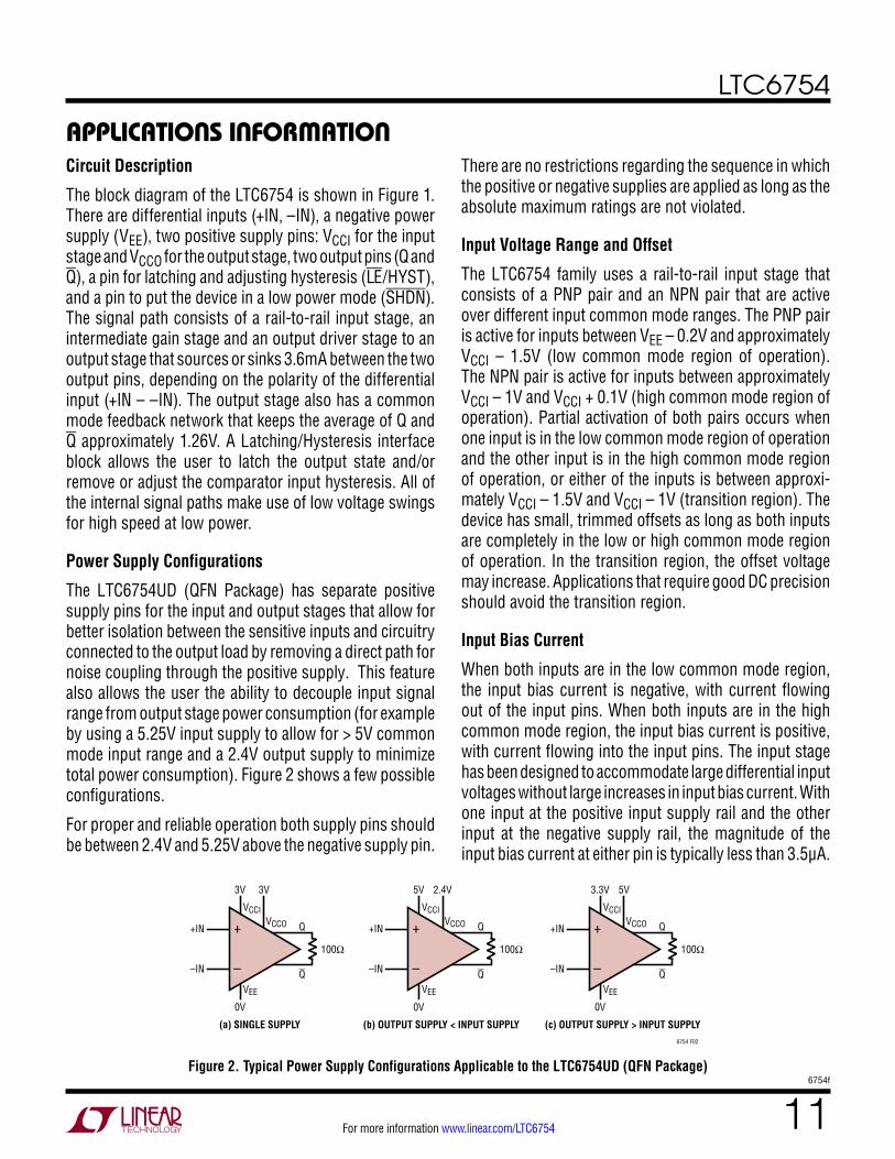
Power Supply Configurations
The LTC6754UD (QFN Package) has separate positive supply pins for the input and output stages that allow for better isolation between the sensitive inputs and circuitry connected to the output load by removing a direct path for noise coupling through the positive supply. This feature also allows the user the ability to decouple input signal range from output stage power consumption (for example by using a 5.25V input supply to allow for > 5V common mode input range and a 2.4V output supply to minimize total power consumption). Figure 2 shows a few possible configurations.
For proper and reliable operation both supply pins should be between 2.4V and 5.25V above the negative supply pin.
applicaTions inForMaTionThere are no restrictions regarding the sequence in which the positive or negative supplies are applied as long as the absolute maximum ratings are not violated.
Input Voltage Range and Offset
The LTC6754 family uses a rail-to-rail input stage that consists of a PNP pair and an NPN pair that are active over different input common mode ranges. The PNP pair is active for inputs between VEE – 0.2V and approximately VCCI – 1.5V (low common mode region of operation). The NPN pair is active for inputs between approximately VCCI – 1V and VCCI + 0.1V (high common mode region of operation). Partial activation of both pairs occurs when one input is in the low common mode region of operation and the other input is in the high common mode region of operation, or either of the inputs is between approxi-mately VCCI – 1.5V and VCCI – 1V (transition region). The device has small, trimmed offsets as long as both inputs are completely in the low or high common mode region of operation. In the transition region, the offset voltage may increase. Applications that require good DC precision should avoid the transition region.
Input Bias Current
When both inputs are in the low common mode region, the input bias current is negative, with current flowing out of the input pins. When both inputs are in the high common mode region, the input bias current is positive, with current flowing into the input pins. The input stage has been designed to accommodate large differential input voltages without large increases in input bias current. With one input at the positive input supply rail and the other input at the negative supply rail, the magnitude of the input bias current at either pin is typically less than 3.5μA.
VCCI
Q
100Ω
Q–
+ VCCO
5V3.3V
VEE
0V
–IN
+IN
VCCI
Q
100Ω
Q–
+ VCCO
2.4V5V
VEE
0V
–IN
+IN
VCCI
Q
100Ω
Q–
+ VCCO
3V3V
VEE
0V
–IN
+IN
6754 F02
(a) SINGLE SUPPLY (b) OUTPUT SUPPLY < INPUT SUPPLY (c) OUTPUT SUPPLY > INPUT SUPPLY
Figure 2. Typical Power Supply Configurations Applicable to the LTC6754UD (QFN Package)
LTC6754
126754f
For more information www.linear.com/LTC6754
applicaTions inForMaTionInput Protection
The input stage is protected against damage from condi-tions where the voltage on either pin exceeds the supply voltage (VEE to VCCI) without external protection. External input protection circuitry is only needed if input currents can exceed the absolute maximum rating. For example, if an input is taken beyond 300mV of either the positive or negative supply, an internal ESD protection diode will conduct and an external series resistor should be used to limit the current to less than 10mA.
Outputs
The LTC6754 has been designed for driving a 100Ω load connected between the output pins to standard LVDS levels, with a differential output voltage of 360mV and a common mode voltage of 1.26V, as described in the Circuit Description Section. See the section on High Speed Board Design Techniques for information on connecting the load to the output pins. The outputs should not be used as CMOS or TTL level outputs, and should not be used for sourcing or sinking excessive load currents.
ESD
The LTC6754 has reverse-biased ESD protection diodes on pins as shown in Figure 1.
There are additional clamps between the positive and negative supplies that further protect the device during ESD strikes. Hot-plugging of the device into a powered socket is not recommended since this can trigger the clamp resulting in large currents flowing between the supply pins.
Hysteresis
Comparators have very high open-loop gain. With slow input signals that are close to each other, input noise can cause the output voltage to switch randomly. Hysteresis is positive feedback that increases the trip point in the direction of the input signal transition when the output switches. This pulls the inputs away from each other, and
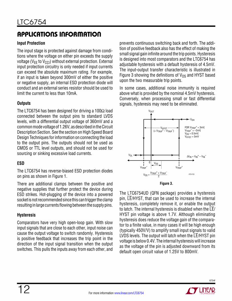
prevents continuous switching back and forth. The addi-tion of positive feedback also has the effect of making the small signal gain infinite around the trip points. Hysteresis is designed into most comparators and the LTC6754 has adjustable hysteresis with a default hysteresis of 4.5mV. The input-output transfer characteristic is illustrated in Figure 3 showing the definitions of VOS and HYST based upon the two measurable trip points.
In some cases, additional noise immunity is required above what is provided by the nominal 4.5mV hysteresis. Conversely, when processing small or fast differential signals, hysteresis may need to be eliminated.
VOH
VOL
0
VOS = 6754 F03
VOUT
VOS
VTRIP+
VHYST(= VTRIP
+ – VTRIP–)
∆VIN = VIN+ – VIN
–
VTRIP+ + VTRIP
–
2
VTRIP–
FOR VTRIP+ = 3mV,
VTRIP– = –2mV,
VOS = 0.5mV,VHYST = 5mV
Figure 3.
The LTC6754UD (QFN package) provides a hysteresis pin, LE/HYST, that can be used to increase the internal hysteresis, completely remove it, or enable the output to latch. The internal hysteresis is disabled when the LE/HYST pin voltage is above 1.7V. Although eliminating hysteresis does reduce the voltage gain of the compara-tor to a finite value, in many cases it will be high enough (typically 450V/V) to amplify small input signals to valid LVDS levels. The output will latch when the LE/HYST pin voltage is below 0.4V. The internal hysteresis will increase as the voltage of the pin is adjusted downward from its default open circuit value of 1.25V to 800mV.
LTC6754
136754f
For more information www.linear.com/LTC6754
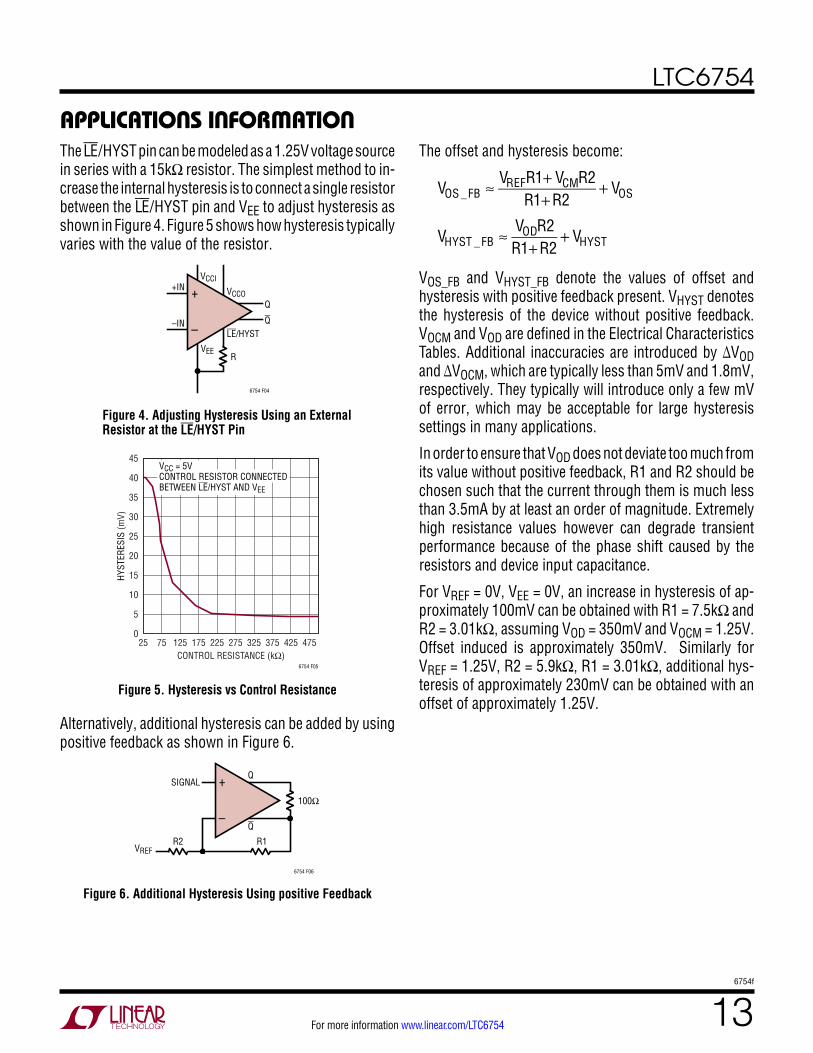
applicaTions inForMaTionThe LE/HYST pin can be modeled as a 1.25V voltage source in series with a 15kΩ resistor. The simplest method to in-crease the internal hysteresis is to connect a single resistor between the LE/HYST pin and VEE to adjust hysteresis as shown in Figure 4. Figure 5 shows how hysteresis typically varies with the value of the resistor.
6754 F04
VCCI
VCCOQ
Q
VEE
LE/HYST
R
–IN
+IN
–
+
Figure 4. Adjusting Hysteresis Using an External Resistor at the LE/HYST Pin
CONTROL RESISTANCE (kΩ)25 75 125 175 225 275 325 375 425 475
0
5
10
15
20
25
30
35
40
45
HYST
ERES
IS (m
V)
6754 F05
VCC = 5VCONTROL RESISTOR CONNECTED BETWEEN LE/HYST AND VEE
Figure 5. Hysteresis vs Control Resistance
Alternatively, additional hysteresis can be added by using positive feedback as shown in Figure 6.
Q
100Ω
Q–
+
VREFR2 R1
SIGNAL
6754 F06
Figure 6. Additional Hysteresis Using positive Feedback
The offset and hysteresis become:
VOS _FB ≈VREFR1+ VCMR2
R1+ R2+ VOS
VHYST _FB ≈VODR2R1+ R2
+ VHYST
VOS_FB and VHYST_FB denote the values of offset and hysteresis with positive feedback present. VHYST denotes the hysteresis of the device without positive feedback. VOCM and VOD are defined in the Electrical Characteristics Tables. Additional inaccuracies are introduced by ΔVOD and ΔVOCM, which are typically less than 5mV and 1.8mV, respectively. They typically will introduce only a few mV of error, which may be acceptable for large hysteresis settings in many applications.
In order to ensure that VOD does not deviate too much from its value without positive feedback, R1 and R2 should be chosen such that the current through them is much less than 3.5mA by at least an order of magnitude. Extremely high resistance values however can degrade transient performance because of the phase shift caused by the resistors and device input capacitance.
For VREF = 0V, VEE = 0V, an increase in hysteresis of ap-proximately 100mV can be obtained with R1 = 7.5kΩ and R2 = 3.01kΩ, assuming VOD = 350mV and VOCM = 1.25V. Offset induced is approximately 350mV. Similarly for VREF = 1.25V, R2 = 5.9kΩ, R1 = 3.01kΩ, additional hys-teresis of approximately 230mV can be obtained with an offset of approximately 1.25V.
LTC6754
146754f
For more information www.linear.com/LTC6754
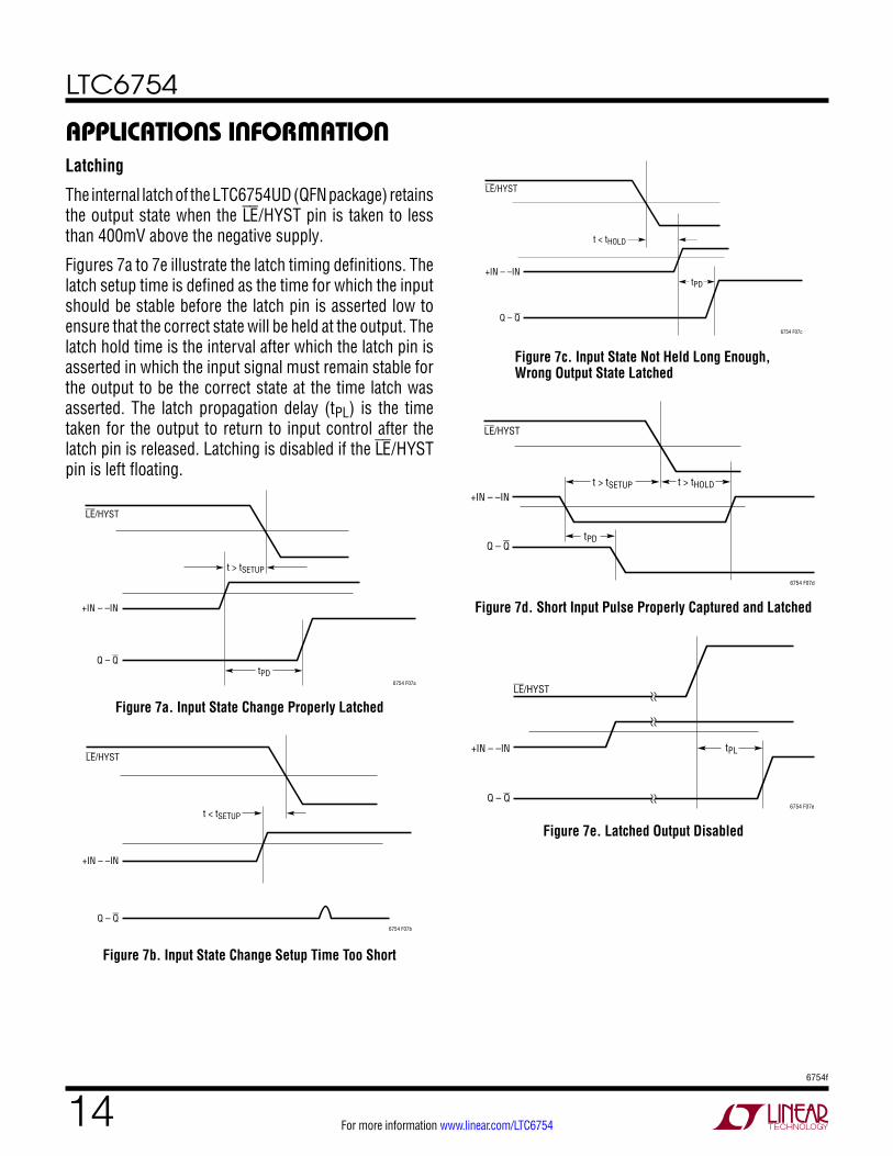
applicaTions inForMaTionLatching
The internal latch of the LTC6754UD (QFN package) retains the output state when the LE/HYST pin is taken to less than 400mV above the negative supply.
Figures 7a to 7e illustrate the latch timing definitions. The latch setup time is defined as the time for which the input should be stable before the latch pin is asserted low to ensure that the correct state will be held at the output. The latch hold time is the interval after which the latch pin is asserted in which the input signal must remain stable for the output to be the correct state at the time latch was asserted. The latch propagation delay (tPL) is the time taken for the output to return to input control after the latch pin is released. Latching is disabled if the LE/HYST pin is left floating.
6754 F07a
+IN – –IN
t > tSETUP
tPDQ – Q
LE/HYST
Figure 7a. Input State Change Properly Latched
6754 F07b
+IN – –IN
t < tSETUP
Q – Q
LE/HYST
Figure 7b. Input State Change Setup Time Too Short
6754 F07c
+IN – –IN
t < tHOLD
tPD
Q – Q
LE/HYST
Figure 7c. Input State Not Held Long Enough, Wrong Output State Latched
6754 F07d
+IN – –INt > tHOLD
tPDQ – Q
LE/HYST
t > tSETUP
Figure 7d. Short Input Pulse Properly Captured and Latched
6754 F07e
+IN – –IN tPL
Q – Q
LE/HYST
Figure 7e. Latched Output Disabled
LTC6754
156754f
For more information www.linear.com/LTC6754
applicaTions inForMaTionShutdown
The LTC6754UD (QFN package) has a shutdown pin (SHDN, active low) that can reduce the total supply current to a typical value of only 1.05mA. When the part is in shut-down, the outputs are placed in a high impedance state. The shutdown pin needs to be taken to within 800mV of the negative supply for the part to shut down. When left floating, the shutdown pin is internally pulled towards the positive supply and comparators remain fully biased on.
Dispersion
Dispersion is defined as the change in propagation delay for different input overdrive or common mode conditions. It becomes very crucial in timing sensitive applications. Overdrive dispersion from 10mV overdrive to 125mV overdrive (150mV total step size) is typically 1ns. The graph titled Propagation Delay vs Common Mode volt-age shows the dispersion due to shifts in input common mode voltage.
Jitter
The LTC6754 has been designed for low phase noise and jitter. This allows it to be used in applications where high frequency low amplitude sine waves need to be converted to full LVDS level outputs with minimal additive jitter. The graph titled Output Jitter vs Input Amplitude demonstrates the additive jitter of the LTC6754 for different amplitudes of a sinusoidal input. Refer to the Electrical Characteristics Table to see how jitter varies with signal frequency.
High Speed Board Design Techniques
In order to obtain optimal performance from the LTC6754, certain guidelines regarding signal routing and power sup-ply bypassing should be carefully followed. If implemented properly, output signal integrity can be maintained, oscil-lations can be eliminated and electromagnetic interference due to fast switching at the outputs can be minimized.
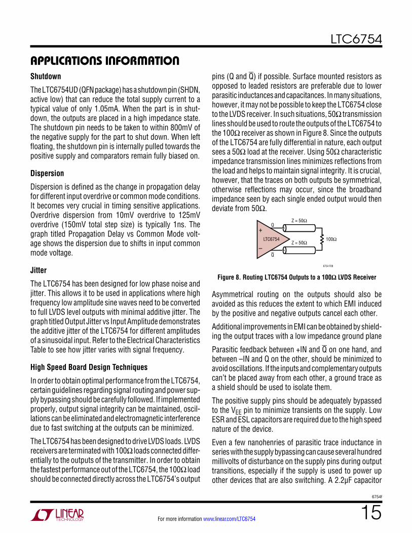
The LTC6754 has been designed to drive LVDS loads. LVDS receivers are terminated with 100Ω loads connected differ-entially to the outputs of the transmitter. In order to obtain the fastest performance out of the LTC6754, the 100Ω load should be connected directly across the LTC6754’s output
pins (Q and Q) if possible. Surface mounted resistors as opposed to leaded resistors are preferable due to lower parasitic inductances and capacitances. In many situations, however, it may not be possible to keep the LTC6754 close to the LVDS receiver. In such situations, 50Ω transmission lines should be used to route the outputs of the LTC6754 to the 100Ω receiver as shown in Figure 8. Since the outputs of the LTC6754 are fully differential in nature, each output sees a 50Ω load at the receiver. Using 50Ω characteristic impedance transmission lines minimizes reflections from the load and helps to maintain signal integrity. It is crucial, however, that the traces on both outputs be symmetrical, otherwise reflections may occur, since the broadband impedance seen by each single ended output would then deviate from 50Ω.
Q
100Ω
Q–
+Z = 50Ω
Z = 50ΩLTC6754
6754 F08
Figure 8. Routing LTC6754 Outputs to a 100Ω LVDS Receiver
Asymmetrical routing on the outputs should also be avoided as this reduces the extent to which EMI induced by the positive and negative outputs cancel each other.
Additional improvements in EMI can be obtained by shield-ing the output traces with a low impedance ground plane
Parasitic feedback between +IN and Q on one hand, and between –IN and Q on the other, should be minimized to avoid oscillations. If the inputs and complementary outputs can’t be placed away from each other, a ground trace as a shield should be used to isolate them.
The positive supply pins should be adequately bypassed to the VEE pin to minimize transients on the supply. Low ESR and ESL capacitors are required due to the high speed nature of the device.
Even a few nanohenries of parasitic trace inductance in series with the supply bypassing can cause several hundred millivolts of disturbance on the supply pins during output transitions, especially if the supply is used to power up other devices that are also switching. A 2.2μF capacitor

LTC6754
166754f
For more information www.linear.com/LTC6754
Typical applicaTionsHigh Speed Clock Recovery and Level Translation Circuit
High speed comparators are often used in digital systems to recover distorted clock waveforms. The LTC6754 can be used to recover a distorted TTL clock signal, and translate it into a signal suitable for driving an LVDS receiver.
In this application, an input clock signal is required to drive an LVDS receiver. If the input signal gets distorted and its amplitude severely reduced due to stray capacitance, stray inductance or due to reflections on the transmission line, the LTC6754 can be used to convert it into a full scale LVDS signal that can drive the receiver.
Figure 10 shows the input and output waveforms of the LTC6754, used to recover a 400mVP–P 340MHz (680Mbps) corrupted clock signal, into a full scale LVDS output signal. AC-coupling could have been used at the input of the comparator, however to preserve input duty cycle information DC-coupling may be preferable, and that is where having a wide input common mode range is an advantage. The input to output delay on the graph is larger than the actual propagation delay. The additional delay is due to the measurement cables.
VCCI VCCO
VEE + 3.3V
6754 F09
340MHzCLOCK INPUT
VEE
VREF = 200mV
LTC6754 100Ω
–
+ Q
Q
LTC6754
Figure 9. Corrupted Clock Recovery to LVDS Translator Circuit.
1ns/DIV
INPUT200mV/DIV
0V
Q OUTPUT
Q OUTPUT
100mV/DIVVOCM = 1.25V
6754 F10
Figure 10. LVDS Output at 340MHz
in parallel with multiple low ESL, low ESR 100nF capaci-tors connected as close to the supply pins as possible to minimize trace impedance is recommended. In many applications the VEE pin will be connected to ground. In applications where the VEE pin is not connected to ground, the positive supplies should still be bypassed to VEE. The VEE pin should also then be bypassed to a ground plane with a 2.2μF capacitor in parallel with low ESL, low ESR 100nF capacitors if possible.
For devices with separate positive input and output supplies, bypass capacitors should be placed from each positive supply to VEE. Capacitors should NOT be placed between the two positive supplies; otherwise disturbances due to output switching can couple back to the inputs.
When the input slew rate is small, sustained oscillations can occur at the output pin while the input is transitioning due to even one millivolt of ground bounce. For applica-tions where the input slew rate is low, internal hysteresis should not be removed by taking the LE/HYST pin high, as the addition of hysteresis makes the comparators more immune to disturbances such as ground bounce. Increas-ing hysteresis by adjusting the LE/HYST pin voltage or by adding positive feedback as discussed in the section on hysteresis can further improve noise immunity. When add-ing positive feedback, surface mounted resistors should be used for R1 and R2 in Figure 6. The resistors should be as close to the device as possible.
applicaTions inForMaTion
LTC6754
176754f
For more information www.linear.com/LTC6754
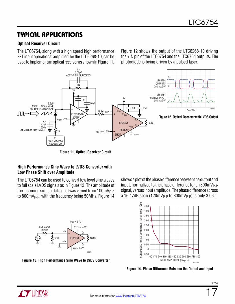
Typical applicaTionsOptical Receiver Circuit
The LTC6754, along with a high speed high performance FET input operational amplifier like the LTC6268-10, can be used to implement an optical receiver as shown in Figure 11.
Figure 12 shows the output of the LTC6268-10 driving the +IN pin of the LTC6754 and the LTC6754 outputs. The photodiode is being driven by a pulsed laser.
100Ω
5V
5V
49.9Ω
14k
–
+LTC6268-10
CF0.05pF
ACCY-P 04021JR05PBS
6754 F11
–
+VCCI
LTC6754
VCCO
VEELE/HYST
SHDN
SHDN
Q
Q
VREF2 = 1.5V
VREF1 = 1V
V–
1k
1nF 10nF
1nF10nF
INPUT
CD3.3nF630V
GRM31BR72J332KW01L
2.5pFAVALANCHE
PHOTODIODELASER
SOURCE
HIGH VOLTAGEREGULATOR
Figure 11. Optical Receiver Circuit
Q
Q
5ns/DIV
LTC6754OUTPUTS
200mV/DIV
LTC6754POSITIVE INPUT
500mV/DIV
6754 F12
Figure 12. Optical Receiver with LVDS Output
shows a plot of the phase difference between the output and input, normalized to the phase difference for an 800mVP-P signal, versus input amplitude. The phase difference across a 16.47dB span (120mVP-P to 800mVP-P) is only 3.06°.
High Performance Sine Wave to LVDS Converter with Low Phase Shift over Amplitude
The LTC6754 can be used to convert low level sine waves to full scale LVDS signals as in Figure 13. The amplitude of the incoming sinusoidal signal was varied from 100mVP-P to 800mVP-P, with the frequency being 50MHz. Figure 14
VCCI = 2.7V
VCCO = 2.7V
–
+ Q
100Ω
Q
6754 F13
SINE WAVE INPUT
VEE = 0.3V
+IN
–INLTC675450Ω
Figure 13. High Performance Sine Wave to LVDS Converter INPUT AMPLITUDE (mVP–P)100 170 240 310 380 450 520 590 660 730 800
–0.50
0
0.50
1.00
1.50
2.00
2.50
3.00
3.50
4.00
4.50
NORM
ALIZ
ED P
HASE
DIF
FERE
NCE,
INPU
T TO
Q –
Q(°
)
6754 F14
Figure 14. Phase Difference Between the Output and Input
LTC6754
186754f
For more information www.linear.com/LTC6754
Both the cable driver and LVDS receiver are implemented using LTC6754's. Figure 18 shows the input clock signal to the cable driver and the outputs of the receiver.
Logic Clock Source to LVDS Cable Driver and Receiver
Figure 17 shows a 250MHz 1.8V logic clock signal being driven across 8 feet of differential Cat6 cable to generate a 250MHz LVDS clock signal at the receiver end.
100Ω100Ω
–
+
3V
6754 F11
VCCI
LTC6754
VCCO
VEEQ
Q+IN
–IN49.9Ω
49.9Ω49.9Ω
–
+
3V
6754 F11
VCCI
LTC6754
VCCO
VEEQ
Q
VREF = 450mV
+IN
–INRJ45RJ45
1.8VCLOCK
SOURCE CAT6 CABLE 8ft
250MHz
(DRIVER) (RECEIVER)
DRIVERINPUT
Figure 17. Logic Clock Source to LVDS Cable Driver and Receiver
1.25ns/DIV
Q
QRECEIVER OUTPUTS
VOCM = 1.25V100mV/DIV
DRIVER INPUT1V/DIV
0V
6754 F18
Figure 18. LVDS Receiver Output, 250MHz
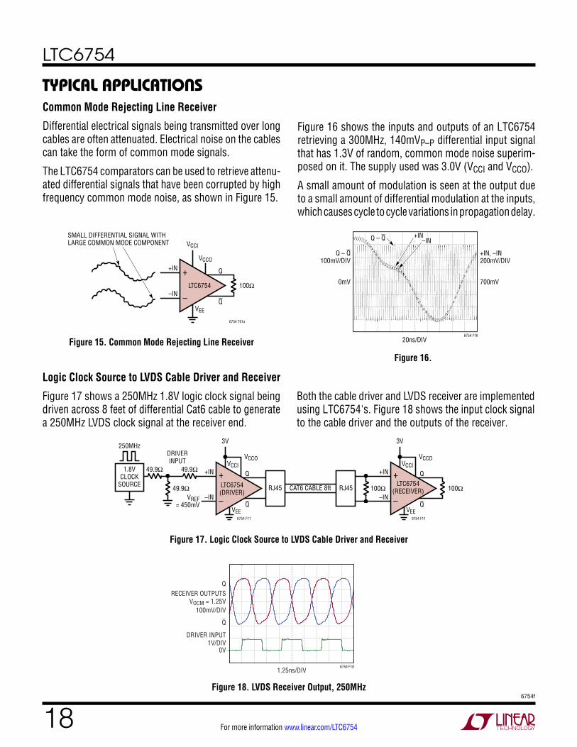
Typical applicaTionsCommon Mode Rejecting Line Receiver
Differential electrical signals being transmitted over long cables are often attenuated. Electrical noise on the cables can take the form of common mode signals.
The LTC6754 comparators can be used to retrieve attenu-ated differential signals that have been corrupted by high frequency common mode noise, as shown in Figure 15.
Figure 16 shows the inputs and outputs of an LTC6754 retrieving a 300MHz, 140mVP–P differential input signal that has 1.3V of random, common mode noise superim-posed on it. The supply used was 3.0V (VCCI and VCCO).
A small amount of modulation is seen at the output due to a small amount of differential modulation at the inputs, which causes cycle to cycle variations in propagation delay.
VCCI
VCCO
–
+ Q
100Ω
Q
6754 T01a
SMALL DIFFERENTIAL SIGNAL WITH LARGE COMMON MODE COMPONENT
VEE
+IN
–INLTC6754
Figure 15. Common Mode Rejecting Line Receiver 20ns/DIV
Q – Q100mV/DIV
0mV
+IN, –IN200mV/DIV
700mV
6754 F16
–INQ – Q +IN
Figure 16.
LTC6754
196754f
For more information www.linear.com/LTC6754
Short Pulse to Differential Cable Driver and CMOS Output Receiver
Figure 19 shows a low amplitude short duration pulse being transmitted over 8 feet of Cat6 differential cable and converted to a full level CMOS output signal. The pulse is applied to the input of an LTC6754. A 150Ω resistor is used along with the 1pF input capacitance of the LTC6754 to limit the rise time at the positive input of the LTC6754,
in order to minimize coupling between the input and other nodes in the system.
The LTC6754 is used to drive 8 feet of cable terminated in a 100Ω resistive load at the inputs of an LTC6752-2, which generates a full scale CMOS logic signal at its output.
Typical applicaTions
50Ω
50ΩCMOS OUTPUT
0.1µF
–
+
3V
6754 F19
VCC
LTC6752-2
VDD
VEE
+IN
–IN
150Ω
–
+
3V
6754 F11
VCCI
LTC6754
VCCO
VEEQ
Q
VREF = 200mV
+IN
–INRJ45RJ45
5ns0V
CAT6 CABLE 8ft
PULSE INPUT400mV
DIFFERENTIALPULSE TRANSMITTER
Q
Figure 19. Short Pulse to Differential Cable Driver and CMOS Output Receiver
2ns/DIV
PULSE INPUT200mV/DIV
0V
CMOS OUTPUT1V/DIV
0V
6754 F20
Figure 20. Pulse Input and Output
LTC6754
206754f
For more information www.linear.com/LTC6754
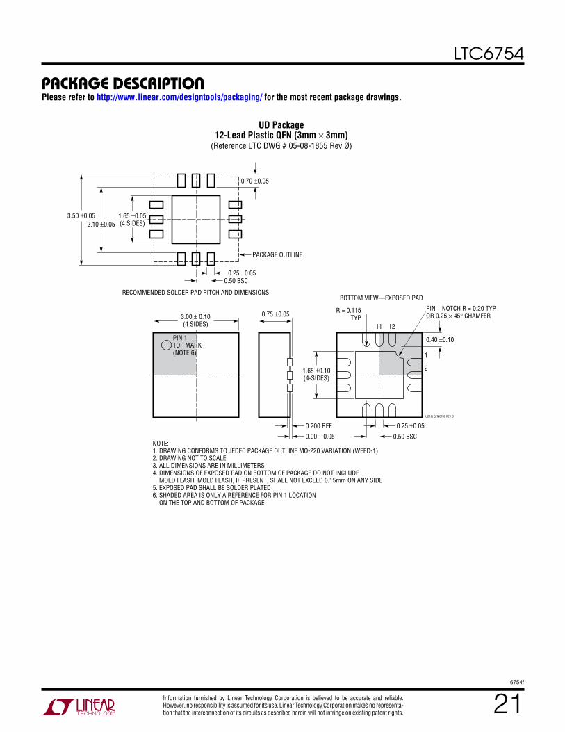
package DescripTionPlease refer to http://www.linear.com/designtools/packaging/ for the most recent package drawings.
1.15 – 1.35(NOTE 4)
1.80 – 2.40
0.15 – 0.30 6 PLCS (NOTE 3)
SC6 SC70 1205 REV B
1.80 – 2.20(NOTE 4)
0.65 BSC
PIN 1
0.80 – 1.00
1.00 MAX
0.00 – 0.10REF
NOTE:1. DIMENSIONS ARE IN MILLIMETERS2. DRAWING NOT TO SCALE3. DIMENSIONS ARE INCLUSIVE OF PLATING4. DIMENSIONS ARE EXCLUSIVE OF MOLD FLASH AND METAL BURR
5. MOLD FLASH SHALL NOT EXCEED 0.254mm6. DETAILS OF THE PIN 1 IDENTIFIER ARE OPTIONAL, BUT MUST BE LOCATED WITHIN THE INDEX AREA7. EIAJ PACKAGE REFERENCE IS EIAJ SC-708. JEDEC PACKAGE REFERENCE IS MO-203 VARIATION AB
2.8 BSC
0.47MAX
0.65REF
RECOMMENDED SOLDER PAD LAYOUTPER IPC CALCULATOR
1.8 REF
1.00 REF
INDEX AREA(NOTE 6)
0.10 – 0.18(NOTE 3)
0.26 – 0.46
GAUGE PLANE0.15 BSC
0.10 – 0.40
SC6 Package6-Lead Plastic SC70
(Reference LTC DWG # 05-08-1638 Rev B)
LTC6754
216754f
For more information www.linear.com/LTC6754
Information furnished by Linear Technology Corporation is believed to be accurate and reliable. However, no responsibility is assumed for its use. Linear Technology Corporation makes no representa-tion that the interconnection of its circuits as described herein will not infringe on existing patent rights.
3.00 ± 0.10(4 SIDES)
RECOMMENDED SOLDER PAD PITCH AND DIMENSIONS
1.65 ±0.05(4 SIDES)
NOTE:1. DRAWING CONFORMS TO JEDEC PACKAGE OUTLINE MO-220 VARIATION (WEED-1)2. DRAWING NOT TO SCALE3. ALL DIMENSIONS ARE IN MILLIMETERS4. DIMENSIONS OF EXPOSED PAD ON BOTTOM OF PACKAGE DO NOT INCLUDE MOLD FLASH. MOLD FLASH, IF PRESENT, SHALL NOT EXCEED 0.15mm ON ANY SIDE5. EXPOSED PAD SHALL BE SOLDER PLATED6. SHADED AREA IS ONLY A REFERENCE FOR PIN 1 LOCATION ON THE TOP AND BOTTOM OF PACKAGE
PIN 1TOP MARK(NOTE 6)
0.40 ±0.10
BOTTOM VIEW—EXPOSED PAD
1.65 ±0.10(4-SIDES)
0.75 ±0.05 R = 0.115TYP
0.25 ±0.05
1
PIN 1 NOTCH R = 0.20 TYPOR 0.25 × 45° CHAMFER
11 12
2
0.50 BSC
0.200 REF
2.10 ±0.053.50 ±0.05
0.70 ±0.05
0.00 – 0.05
(UD12) QFN 0709 REV Ø
0.25 ±0.050.50 BSC
PACKAGE OUTLINE
UD Package12-Lead Plastic QFN (3mm × 3mm)
(Reference LTC DWG # 05-08-1855 Rev Ø)
package DescripTionPlease refer to http://www.linear.com/designtools/packaging/ for the most recent package drawings.

LTC6754
226754f
For more information www.linear.com/LTC6754 LINEAR TECHNOLOGY CORPORATION 2015
LT 0815 • PRINTED IN USALinear Technology Corporation1630 McCarthy Blvd., Milpitas, CA 95035-7417(408) 432-1900 FAX: (408) 434-0507 www.linear.com/LTC6754
relaTeD parTs
Typical applicaTion
PART NUMBER DESCRIPTION COMMENTS
High Speed Comparators
LTC6752/LTC6752-1/LTC6752-2/LTC6752-3/LTC6752-4
2.9ns 280MHz CMOS Output Comparators RR Inputs. Can drive 1.8V logic directly (LTC6752-2/LTC6752-3/LTC6752-4)
LT1715 4ns 150MHz Dual Comparators 4.6mA at 3V
LT1720/LT1721 Dual/Quad 4.5ns Single Supply Comparators 4mA/Comparator
LT1711 High Speed Rail-to-Rail Comparators 3V/5V/±5V, 4.5ns at 20mV Overdrive
LT1116 12ns Single Supply Ground Sensing Comparator Inputs Can Exceed Positive Supply Up to 15V Without Damaging Device
Clock Buffers/Logic Converters
LTC6957-1/LTC6957-2/LTC6957-3/LTC6957-4
Low Phase Noise, Dual Output Buffer/Driver/Logic Converter
LVPECL/LVDS/CMOS Outputs, Additive Jitter 45 fsRMS
High Speed Operational Amplifiers
LTC6252/LTC6253/LTC6254
Single/Dual/Quad 3.5mA 720 MHz 280V/μs, 2.75nV/√Hz, Rail-to-Rail I/O
LTC6268/LTC6269 Single/Dual 500MHz Ultra Low Bias Current RR Outputs
LTC6268-10/LTC6269-10 Single/Dual 4GHz Ultra Low Bias Current RR Outputs, Gain of 10 Stable
LTC6246/LTC6247/LTC6248
Single/Dual/Quad 1mA, 180MHz 90V/μs, 4.2nV/√Hz,Rail-to-Rail I/O
15 Bit PRBS 250Mbps Logic Signal to LVDS Converter Eye Diagram Test Setup
16.7Ω
16.7Ω
1GHz BY 4
VCCI VCCO
SAMPLING OSCILLOSCOPE
3.3V
3.3V
3.3V
6754 TA02a
40mA200Ω
VEE
FUNCTION =CH1 – CH2LTC6754
FPGA250Mbps
15bit PRBS–
+ Q
Q
LTC6754
6in COAX
6in COAX
100Ω
TRGR
CH1
CH2
200Ω40mA
LTC2000
+IN
–IN
1k
1k2ns/DIV
DIFFERENTIAL OUTPUT
200 mV/DIV
6754 TA02b


